1
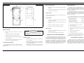
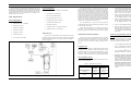
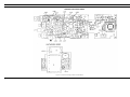
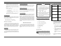
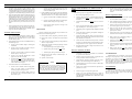
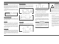
LBI-38557A
Mobile Communications
SERVICE SECTION
FOR
MPI-II VHF PERSONAL RADIO
Ericsson GE Mobile Communications Inc.
Mountain View Road•Lynchburg, Virginia 24502
Copyright January 1991, Ericsson GE Mobile Communications, Inc.
Maintenance Manual
Printed in U.S.A.
LBI-38557
LBI-38557
INTRODUCTION
TABLE OF CONTENTS
Page
INTRODUCTION.................................................................................................................................
1
DISASSEMBLY PROCEDURE ..........................................................................................................
TOOLS NEEDED..........................................................................................................................
BATTERY ......................................................................................................................................
FRONT COVER ............................................................................................................................
SYNTHESIZER BOARD .............................................................................................................
REAR COVER...............................................................................................................................
BNC CONNECTOR......................................................................................................................
UDC COVER.................................................................................................................................
TOP COVER ..................................................................................................................................
SIDE PANEL..................................................................................................................................
1
1
1
2
2
2
2
2
2
2
PERSONALITY PROGRAMMING ...................................................................................................
PROGRAMMING .........................................................................................................................
2
2
ALIGNMENT AND TEST ...................................................................................................................
TEST EQUIPMENT ......................................................................................................................
TEST SETUP .................................................................................................................................
TRANSMITTER ALIGNMENT ..................................................................................................
RECEIVER ALIGNMENT ...........................................................................................................
2
3
3
3
5
TROUBLESHOOTING........................................................................................................................
TRANSMITTER............................................................................................................................
RECEIVER ....................................................................................................................................
SYNTHESIZER.............................................................................................................................
5
5
6
6
COMPONENT REPLACEMENT .......................................................................................................
SURFACE MOUNT COMPONENTS .........................................................................................
SURFACE MOUNT REMOVAL .................................................................................................
SURFACE MOUNT COMPONENT REPLACEMENT.............................................................
SURFACE MOUNTED INTEGRATED CIRCUIT REPLACEMENT......................................
MODULE REPLACEMENT ........................................................................................................
7
7
7
8
8
8
PREVENTIVE MAINTENANCE .......................................................................................................
8
BATTERY INFORMATION ................................................................................................................
REDUCED CAPACITY ................................................................................................................
8
8
MODIFICATION INSTRUCTIONS ...................................................................................................
9
FIGURES
Figure 1 - Removing The Battery Pack ........................................................................................
Figure 2 - Disassembly..................................................................................................................
Figure 3 - Test Setup......................................................................................................................
Figure 4 - Location Of Tuning Controls And Test Points............................................................
Figure 5 - Reference Oscillator (Input To PLL U201).................................................................
Figure 6 - Fin (Input to U201) .......................................................................................................
Figure 7 - Remp (Generated In U201)..........................................................................................
Figure 8 - SYN EN (Input To Pin 13 Of U201) ...........................................................................
Figure 9 - Typical Ni-Cad Cell Discharge Curve.........................................................................
Figure 10 - Alternate IF Option.....................................................................................................
1
2
3
4
7
7
7
7
8
8
This service section contains the necessary information
to align and troubleshoot the MPI-II (136-174 MHz) Personal Radio. This manual includes steps for disassembly and
procedures for replacing surface mount components and
integrated circuits. Preventive maintenance checks are provided as well as battery service data. The tests and procedures in this manual are intended to be used by a qualified
service technician.
In order to perform many of the following alignments,
tests and troubleshooting checks it will be necessary to
program the radio’s personality EEPROM to tailor the operation of the radio to stipulated requirements. Instructions
are offered which include the use of an IBM compatible
personal computer and appropriate software. If the radio is
properly functioning and has a preprogrammed personality,
alignment procedures can be initiated directly.
Conventional testing using the recommended alignment
procedures will verify proper operation of all of the radio’s
circuitry, with the following exceptions:
•
•
NOTE:TORX® is a Registered Trademark of Camcar
Division of Textron Inc.
BATTERY
CAUTION
ALWAYS remove the battery pack before disassembling the unit to avoid blowing the fuse or causing
other component damage.
1.
Turn the radio OFF.
2.
Place thumb on bottom of battery pack and press
battery pack toward the top of the radio as shown in
Figure 1.
3.
While pressing the battery pack toward the top of the
radio, push bottom of battery pack away from the
radio.
Data modulation circuitry in transmit mode
Data demodulation circuitry in receive mode
DISASSEMBLY PROCEDURE
The following section describes how to gain access to
the Transmit/Receive Board and the Synthesizer Board for
servicing. This section also provides the procedures to disassemble various assemblies from the radio.
TOOLS NEEDED
1.
No. 7 TORX®screwdriver
2.
No. 8 TORX®screwdriver
3.
.050 hex tool
4.
Flat blade screwdriver
5.
ST2312 spanner tool
6.
ST2311 spanner tool
7.
5/16 wrench
Figure 1 - Removing The Battery Pack
WARNING
Do not dispose of battery packs or batteries by
burning. To do so may cause an explosion.
1
S
E
R
V
I
C
E
S
E
C
T
I
O
N
LBI-38557
LBI-38557
BNC CONNECTOR
1.
Remove the No. 3-48 x .125 setscrew (D) using a 0.050
hex tool.
2.
Unsolder the BNC center pin from the antenna contact.
3.
Remove the BNC connector.
UDC COVER
Remove the M2.5-0.45 screw using a flat blade screwdriver or the edge of a coin.
TOP COVER
1.
Pull off the two knobs from the ON/OFF/VOLUME
and the Squelch control.
2.
Remove the Spanner nuts (E) using a Spanner Tool
ST2311.
3.
Remove the 1/4-40 (F) nut using a 5/16 wrench.
4.
Remove the top cover from the T/R assembly.
Figure 2 - Disassembly
SIDE PANEL
FRONT COVER
CAUTION
1.
2.
Remove the battery as described in the previous
section.
Remove the two screws at (A) (See Figure 2).
3.
Carefully lift the front cover from the radio.
4.
Unplug the cable between the front cover MIC Board
and the T/R Board.
5.
To gain access to the microprocessor, remove the
three screws at (B) and lift up the cover.
When separating the Synthesizer and Transmit/Receive boards, care should be taken not to bend the
connector pins.
2
2.
Remove the two Audio Jack Spanner nuts (G) using a
Spanner Tool ST2312.
Remove the side panel from the T/R Assembly.
PERSONALITY PROGRAMMING
REAR COVER
1.
Remove the screw at (C) using a No. 7 TORX screwdriver (See Figure 2).
2.
Remove the four M2 pan head screws, 3 at (B) and 1
at (H), on the component side of the T/R Board using
a No. 7 TORX screwdriver.
3.
The RF Board with the top cover and the side panel
attached may now be removed from the rear cover.
SYNTHESIZER BOARD
The Synthesizer Board may be separated from the
Transmit/Receive Board by prying the connectors straight
out from the pins.
1.
The MPI-II Personal Radio is equipped with a 256 x 8 bit
serial personality EEPROM. All cutomer information such as
the customer frequencies, customer tones and customer options are stored in the EEPROM. The EEPROM contains all
information to tailor the operation of the radio to the user’s
requirements. The EEPROM is programmed by using an IBM
compatible personal computer with MSDOS, Interface Box
19D438367G1, RS-232 Cable 19B235027P1, Programming
Cable TQ-3352 and Programming Software TQ-3351.
PROGRAMMING
The MPI-II radio is programmed through a test cable
connected to the accessory connector located on the side of the
radio. Power is applied to the battery terminals located on the
rear radio assembly. B+ should be 7.5V for a 2 watt radio and
10.0V for a 4 watt radio.
Programming information must be written to the personality PROM before alignment or performance tests. This is
always done through the accessory connector and cable. This
cable may be attached to the radio and left connected during
the entire test procedure.
The assigned frequencies to be used should be programmed into the personality of each 2-channel radio:
First Transmit frequency
First Receive frequency
Tx F1
Rx F1
Second Transmit frequency
Second Receive frequency
Tx F2
Rx F2
The radio’s chosen options must alos be programmed in:
•
•
•
•
•
•
•
Channel Guard (with C.G. frequency)
No Channel Guard
Digital Channel Guard (with D.C.G. code)
Type 99 Tone (with Tone A Frequency, Tone B Frequency)
Talk-around (enable, disable)
STE (enable, disable)
Channel Busy Inhibit (enable, disable)
Detailed programming instructions should be followed as
found in the TQ-3351 Programming Manual.
ALIGNMENT AND TEST
Initially, the Receiver of the MPI-II Personal Radio is
aligned and ready for use before leaving the factory. The
Transmitter is tuned at the high end of the band, with retuning
recommended for optimum operation when another frequency
is selected. This section provides procedures for aligning and
testing the MPI-II VHF (136-174 MHz) Personal Radio.
LBI-38557
LBI-38557
Several tests are presented which will help isolate a possible RF or control circuit problem. The control circuits, which
are located on the T/R Board, contain no adjustments and there
is no alignment required for the control circuits. See the Troubleshooting section for test information if a problem is suspected in the control circuits.
TEST EQUIPMENT
General Equipment
1.
RF Generator (136-174 MHz)
2.
Wattmeter (5 watts)
3.
Ammeter (2 amperes)
4.
Distortion Analyzer
5.
Frequency Counter
6.
Test Box TQ-0613
7.
Test Cable 19C851752P8
Special Equipment
1.
IBM Compatible Computer with MS-DOS
2.
Interface Box 19D438367G1
3.
RS-232 Cable19B235027P1
4.
Programming Cable TQ-3352
5.
Programming Software TQ-3351
6.
Synthesizer Extender Cable
7.
Discharge Analyzer
8.
Alignment Tool, 0.1" slotted (metal) tips
9.
Alignment Tool, 0.1" slotted tips.
Connect the leads of the dummy battery to the two
battery terminals accessble in the open radio. The external
power leads from the dummy battery will be connected later.
Connect the TQ-0613 Test Box to the radio using the UDC
connector. An audio oscillator can be used as an audio input
to the Text Box. Connect a distortion analyzer to the audio
output of the Test Box. For transmitter operation, an RF
power meter/modulation analyzer should be connected to the
antenna connector J3 in place of the antenna. A frequency
meter can be coupled to the output using a coaxial directional
coupler. For receiver operation a frequency modulated RF
signal generator should be connected to J3.
For programming, the TQ-3301 serial programmer
would alternatively be connected through the UDC connector on the side of the radio.
1.
With the highest transmitter frequency selected, tune
C118, C124, C126 for maximum output power measured with the Power Meter. The power out should be
greater than 4.5 watts with 10V supply and greater
than 2.5 watts with 7.5V supply.
2.
Adjust C126 for minimum DC current drain from the
power supply until the power output is 4.2-4.3 watts
for 10V supplies and 2.2-2.3 watts for 7.5V supplies.
3.
Adjust C118 for minimum DC current drain from the
power supply until the power output is 4.0-4.1 watts
for 10V supplies and 2.0-2.1 watts for 7.5V supplies.
4.
Tune C124 for maximum outut power.
5.
Return C126 for 1050 mA (±10 mA) for 10V supplies and 750 mA (±10 mA) for 7.5V supplies. Check
the output power. The output power should be equal
to or greater than the minimum power as listed in the
table above.
Set the DC power supply to 7.5 volts(±0.1 volts) for a 2
watt radio, or 10 volts (±0.1 volts) for a 4 watt radio. Connect
the power supply to the dummy battery as shown in Figure
3.
S
E
R
V
I
C
E
TEST SET UP
Customer Programming And Wide Band
Tuning
TRANSMITTER ALIGNMENT
To gain access to adjustable circuit components for alignment of the radio, the front cover must be removed as described
in the Disassembly Section. A test setup should be arranged as
shown in Figure 3.
With the test setup for transmitter operation in place,
select the highest transmit frequency and key the radio ON
to find an indication of output power on the power meter.
See Figure 4 for the location of tuning controls and test
points.
This section describes the programming and adjustments for wide band tuning. The following steps (1-4) are
for preset customer frequencies with:
– Up to 10 MHz spread with no degradation from Pref
Frequency Set
– Up to 17 MHz spread with less than 1 dB of degradation from Pref in the 136-153 MHz band
Measure the frequency of the RF output signal with the
frequency meter. It should be within ±100 Hz of the programmed frequency. Should a small adjustment be necessary, this change can be made by tuning the Reference
Oscillator (TCXO) module U203 on the Synthesizer Board.
Set Transmitter Power
The following sequence should be followed for maximizing rated output power:
Table 1 - Minimum Output Power
2 WATT
RADIOS
4 WATT
RADIOS
Battery or Supply
Voltage
7.5
VOLTS
10
VOLTS
Minimum Output
Power
1.9
WATTS
3.8
WATTS
or
– Up to 24 MHz spread with less than 1 dB of degradation from Pref in the 150-174 MHz band
1.
Frequency spreads greater than 10 MHz only Program the radio on a channel mid way between the
two desired frequencies. Tune the radio by following
Steps 1-5 in the Set Transmitter Power section. Then
reprogram the customer frequencies and measure the
power out on the upper channel. Go to Step 2.
Frequency spreads less than or equal to 10 MHz
only -Program the radio on the customer frequencies. Tune the radio on the higher frequency channel
by following Steps 1-5 in the Set Transmitter Power
section.
Figure 3 - Test Setup
3
S
E
C
T
I
O
N
LBI-38557
LBI-38557
Figure 4 - Location of Tuning Controls and Test Points
4
LBI-38557
2.
3.
4.
LBI-38557
Check power on the lower channel. Adjust C124 in the
direction that increases power output to a level half way
between the initial lower and upper channel levels.
Recheck the upper channel power. If the upper channel
power is reduced, reset to the previous level by adjusting C126.
Repeat this procedure until the power out on both
channels is equal (±.1W).
•
•
For frequency spreads ≤ 10 MHz - power out ≥
power minimum
For frequency spreads > 10 MHz - power out ≥
power minimum - 1dB
Supply current levels should not exceed 1100 mZ
(10V) or 800 mA (7.5V) with wide band tuning.
TX Modulation Set
With the transmitter keyed, apply a 1 kHz tone at 100 mV
RMS to the MIC input. Adjust R230, located on the Synthesizer Board, until the following peak deviation is measured on
the output modulation analyzer:
With Channel Guard - 4.5 kHz (±100 Hz)
Without Channel Guard - 3.75 kHz (±100 Hz)
Second LO Frequency Set
Remove all modulation from the input signal and increase
the level to 0 dBm. Monitor the frequency at J501 and adjust
L505 in the crystal oscillator circuit for 455 kHz ±100 Hz.
Modulate the RF input signal with a 1 kHz tone at 3 kHz
peak deviation. Load the speaker output at the accessory connector with 8 ohms to ground. Monitor the speaker output from
the accessory connector while tuning L506 in the quardrature
detector for a maximum audio level.
L.O. Notch Tuning
When it necessary to limit the L.O. leakage out the antenna
port to a level less than -60 dBm, (Canadian D.O.C. RSS 119,
121 require -53 dBm for portables with batteries, otherwise -57
dBm) the L.O. notch filter may be tuned to the receiver L.O.
frequency to meet this requirement. Observe the L.O. signal
level at the antenna port on a spectrum analyzer capable of
reading -70 dBm. Select the channel with the lower operating
receive frequency and tune the notch filter adjustable capacitor
(C136) for a minimum level. Check the level on the higher
receive frequency. If greater than -60 dBm, turn the capacitor
(C136) in the direction that lowers the level to the point that
-60 dBm is reached and stop. Recheck the lower receive
frequency.
TROUBLESHOOTING
IF Alignment
This section provides a guide to troubleshooting the MPIII VHF radio. The following procedures will assist in determing if the problem is in the RF circuits (Transmitter,
Receiver or Synthesizer) or the Control circuits. The test set-up
should be the same as that used in the Alignment section of this
manual.
Tabel 2 - General Troubleshooting Guide
Throughout the service procedures, the following
information should be observed:
•
Quadrature Detector Set
RECEIVE ALIGNMENT
Change to a receiver test setup, with a frequency modulated RF signal generator connected to the antenna jack J3. Set
the input RF signal to the highest programmed receive frequency and modulate it with a 1 kHz tone at 5 kHz peak
deviation. Use a signal level high enough to measure the level
of the 455 kHz 2nd IF signal at test point J501 with an RF AC
voltmeter. Proceed with the following alignment procedure.
NOTE
•
•
•
The bench power should be set for 7.5 Vdc
(±0.1 Vdc) for a 2 watt radio, or 10.0 Vdc (±0.1
Vdc) for a 4 watt radio. If a battery pack is
used, it should be fully charged. Typical battery
pack voltage should be within ±20% of set
voltage over its full discharge cycle.
Logic Levels should be:
Logic 1 = high ≤ 4.5 Vdc
Logic 0 = low ≥ 0.5 Vdc
The personality information stored in the radio
should be backed up on the PC computer before
any service procedure.
•
•
•
•
•
•
•
•
•
•
•
Dead Battery Pack
Fuse blown
Control circuit problem
At power-up radio
beeps continuously
•
•
•
Weak battery pack
Unit is not programmed
Synthesizer is not locked
Receiver inoperative
or weak
•
•
•
•
Squelch level set too high
Channel Guard enabled
Defective antenna
T/R Board problem
Transmitter inopeative or low range
•
•
•
•
Power levels set too low
Weak battery
Defective antenna
T/R Board problem
Tx and Rx inoperative on one or both
channels
RX and TX block diagrams with RF gains and
levels
•
•
S
E
R
V
I
C
E
S
E
C
T
I
O
N
Programming incorrect
Synthesizer problem:
VCO, prescaler, or
lock detect
Interconnection diagram
troubleshooting a personal radio. Current consumption offers an excellent clue in the case of a dead or
weak transmitter. See Table 3 in the Battery Information section on typical current consumption for different operating conditions. Check supplies as
follows:
Outline diagrams
a.
Check for battery B+ voltage at J12-01, or inside
fuse F1/switch S1. It should be present at the
driver Q104 and final amplifier Q105, and measure 7.5 Vdc for 2-watt radio, 10 Vdc for 4-watt
radio.
b.
Check for presence of B+ SW on buffer amplifier Q106 and predriver Q103. It should switch
ON under control of the PTT switch through B+
switch Q805.
c.
Check 5.4 V from 5.4 V regulator, which is
required for and available on the Synthesizer
board.
Synthesizer block diagram
Control Circuits block diagram
Audio Processing block diagram
Schematic diagrams
Parts lists
IC data
Adjust the RF signal level for linear operation at J501.
Tune L502 and L504 for a maximum IF signal level at J501.
TRANSMITTER
An alternate method for making the IF alignment is as
follows. Tune L502 and L504 for minimum audio distortion
while monitoring the speaker output. Use either 5 kHz or 3 kHz
of deviation.
Transmit Power Output Problem, Inoperative
or Low
1.
POSSIBLE CAUSES
Completely inoperative (no audio)
Modules are not field repairable. Schematics
and Outline drawings for the modules are presented for troubleshooting reference only.
Documentation To Help In Troubleshooting
•
SYMPTOM
Power sources and regulated power supplies should
be checked before troubleshooting any transmitter
problem. The radio’s power source, whether a battery
or bench power supply, is especially important in
2.
An early step in troubleshooting for the cause of low
RF output power is to check that the programming is
correct.
5
LBI-38557
3.
4.
LBI-38557
Check for proper operation of the synthesizer. There
should be approximately 0 dBm drive level on the
SYNTH output line for proper transmit operation. If
a Syntheiszer problem is suspected, following the
suggestions in Troubleshooting Synthesizer section.
Check to see that Channel Guard signal is at the
output of the post limiter filter, U301-A pin 1, or
at the TX MOD output.
If the TX MOD output is proper from the T/R Board,
then check to see if the audio signal is arriving at the
Synthesizer Board. If so, on the Synthesizer Board:
The following steps are suggested to locate the trouble:
1.
Be sure the programming is correct.
a.
Check to see if the audio is at Mod Pot R230 pin
1.
2.
Check to see if the receiver is unsquelched with strong
on-channel signal: CAS is low, as controlled by SQ
POT R619.
b.
Check to see if the audio level at the centertap of
Mod Pot R230 changes with pot setting.
3.
Check the RX MUTE and MUTE gates are in correct
states.
Check that the audio signal is arriving at the
VCO U204 pin 3.
4.
In the voice path check that audio is reaching the output
stage U602-B pin 7, and its output on pin 1.
RECEIVER
5.
Check that power is applied to audio amplifier U602-B
pin 2.
Receiver problems will generally only be found on the
T/R Board, in the following sectors:
6.
4.
If current consumption appears normal, and the synthesizer output level is correct, check that the DPTT
and BAND SW lines are in the proper state. The
problem may be in the antenna T/R switch circuit
with diodes D101, D102 or in the antenna connector
W1. A problem in the antenna switch circuit or the
antenna connector may also cause the receiver to be
weak.
c.
5.
If the synthesizer drive level seems normal, but current consumption is low, the transistor stages in the
transmitter RF chain should next be checked, beginning with the final amplifier Q105.
Transmit Audio Problem
1.
2.
For a transmit audio problem the trouble could be
either in the Syntheiszer Board or the T/R Board.
Monitoring the TX MOD line for correct audio
should identify which.
If the problem seems to be on the T/R Board, then try
the following steps:
a.
Check to see if the MIC output is reaching the
T/R Board.
b.
Check to see if the audio is present at the preamplifier output, collector of Q301.
c.
d.
e.
3.
Check to see if the MIC MUTE line is in the
proper state, low for not muted.
Check that the PTT is arriving at the microprocessor U701 pin 7. This is the command to generate the DPTT and BAND SW signals along
with the MIC MUTE signal.
If Channel Guard is to be transmitted, then:
a.
b.
c.
6
Check to see if the audio is present at the audio
limiter output, U301-D pin 14.
Check to see if Channel Guard is being generated at CG ENC output by microprocessor
switching outputs U701 pins 34-37.
Check to see if the Channel Guard signal is at
the output of the Tx Channel Guard low pass
filter U603-A pin 1.
Receive Audio Problem, Low Audio Level Or No
Audio
•
•
•
•
•
•
Receiver RF circuitry beginning at antenna jack J3
Three paths of audio processing beginning with the
VOL SQ HI signal:
1.
Voice path, through to the speaker output
2.
Squelch noise path, through to CAS output
3.
Tone data path, through TN DATA output
Microprocessor and circuitry controlled by it, including synthesizer
Receiver Squelch Problem
Check for presence of noise at VOL SQ HI line when
no received RF carrier is present.
2.
In the squelch noise path check for presence of filtered
noise at output of high pass filter U501 pin 11.
3.
Check to see if the noise level at U501-11 decreases
when a RF signal is input to the receiver.
4.
With no carrier, be sure noise is present at pin 1 of
squelch pot R619, and also at U603 pin 12 when
squelch pot is rotated.
Check that audio is reaching the speaker through the
Accessory Jack Board.
5.
Check that the DC level of the filtered noise output
measured at U603-B pin 6 varies with RF signal level.
7.
Check that when channel guard is used the tones are
found on the TN DATA line. When T99 tones are used
they should be at TN DATA.
6.
Make certain that a threshold voltage is present at
comparator input U603-B pin 5.
8.
Check that data reaches the microprocessor, and that
the receiver is unmuted when correct limited tone channel guard data or correct Type 99 tones are decoded.
7.
Check to see if the CAS line switches low when a RF
signal carrier is introduced.
8.
Check that the DC level at the threshold terminal U603B pin 5 increases when the voltage of the CAS line
increases.
9.
Make certain that the CAS line switching voltage
reaches the microprocessor input U701 pin 13.
9.
If digital channel guard is being used, check to see if
the polarity is correct.
Receiver Sensitivity Problem
1. Check that 5.4 V, RX 5.4 V, SYNTH 5.4 V, and VREF
are present where indicated.
SYNTHESIZER
2.
Check to see if the antenna clip W1 is soldered to the
center pin of BNC antenna connector J3.
3.
Check that DC voltages in the RF stages are correct.
(Refer to the schematic diagram in LBI-38555).
4.
Check that RF gains are correct. (Refer to Block Diagram in LBI-38555).
Troubleshooting the synthesizer circuit consists of first
checking for the proper D.C. levels. Then determing if proper
waveforms are present and checking individual modules.
When the channel switch or the PTT switch is operated, the
SYN ENABLE, SYN DATA and SYN CLK should become
active. Monitor these lines and troubleshoot the Transmit/Receive Board if activity does not occur.
5.
Check to see if the first and second LO injection frequencies are correct.
6.
Check for proper LO injection signal levels.
7.
Check to see if the quadrature detector is tuned for
maximum audio output level at the speaker when an
input RF signal is modulated with a 1 kHz tone at 3 kHz
peak deviation.
Speaker, at final output
NOTE
To facilitate testing of receiver problems, the battery saver mode can be disabled by shorting the
TEST input to the microprocessor to ground during
power-up. The radio can be taken out of test mode
by recycling the power without TEST grounded.
If a sensitivity problem or a distortion problem remains,
then a receiver RF and IF alignment should be done
using the recommended procedures in the alignment
section.
1.
Receiver IF circuitry, 45 MHz 1st IF and 455 kHz
2nd IF
Source of audio signals beginning at the quadrature
detector output in U501
8.
TX Modulation
Check to see if the audio is at pin 1 of the Mod Pot R230.
The audio level at pin 2 of the Mod Pot should change when
the pot is rotated. Finally, check to see if the audio signal is
arriving at pin 5 at U206.
LBI-38557
LBI-38557
D.C. Analysis
Bilateral Switch U205
CAUTION
Battery voltage (7.5/10 Volts, B+) is supplied to a 5.4 volt
regulator circuit consisting of transistors Q801, Q802 and
Q803. Diode regulator U801 provides a 2.5 volt reference for
this circuit. Battery voltage (B+) is also supplied to the Synthesizer Board for isolation amplifier U206. the 5.4 volt regulator supplies both the synthesizer and most of the Transmit
and Receive circuits.
Bilateral switch U205 is used to short around parts of the
loop filter during channel changes. A shorted gate (to ground
or adjacent gate) may be isolated by comparing voltages
through the loop filter to those of a functioning radio. Defective
gates might be suspected when the radio does not change
frequency quickly enough.
Figure 8 - SYN EN (Input to Pin 13 of U201)
The BAND SW control input, initiated from the Transmit/Receive Board, is used to bandswitch the VCO. This input
is low when receiving and high (greater than 3 volts) when
transmitting.
COMPONENT REPLACEMENT
Figure 5 - Reference Oscillator
(Input to PLL Module U201, Pin 2)
Reference Oscillator U203
Pin 2 of the Phase Lock Loop U201 should have a waveform similar to the one shown for the reference oscillator
(Figure 5). If this waveform is not present, oscillator module
U203 is probably defective.
Figure 6 - Fin (Input to U201, Pin 10)
VCO U204
Transistor Q201
Connect a DC power supply to pin 3 of U204. With 2.0
volts DC on pin 3, the output on pin 5 of U204 should be
approximately 140 MHz for the low split and approximately
190 MHz for the high split. With 4.3 volts DC on pin 3, the
output should be approximately 220 MHz for the high split.
Power output of the VCO can be measured by connecting
a coax cable directly to the module, between pin 5 and ground,
through a 100 pF coupling capacitor. The output should be
approximately 0 dBm.
S
E
R
V
I
C
E
SURFACE MOUNT COMPONENTS
NOTE
Waveforms associated with the synthesizer were
measured with 10 megohms, 30 pF probe using Dc
coupling. See Figures 5-8.
The CMOS Integrated Circuit devices used in this equipment can be
destroyed by static discharges. Before handling one of these devices,
the serviceman should discharge
himself by touching the case of a bench test instrument that has a 3-prong power cord connected to an
outlet with a known good earth ground. When soldering or desoldering a CMOS device, the soldering equipment should have a known good earth
ground.
After checking for the proper operation, measure the loss
of the VCO, pin 5 to pin 1 of the Prescaler U202. The loss
should be 10 dB.
The top of the ramp is approx. 0.8 Vdc geater than
the control voltage out on pin 17 of U201.
Surface mount components should always be replaced
using a temperature controlled soldering system. The soldering tools may be either a temperature controlled soldering
iron or a temperature controlled hot-air soldering station. A
hot-air system is recommended for the removal of components on the multi-layered boards used in the MPI-II radio.
With either soldering system, a temperature of 700°F
(371°C) should be maintained.
The following procedures outline the removal and replacement of surface mount components. If a hot-air soldering system is employed, see the manufacture’s operating
instructions for detailed information on the use of your
system.
SURFACE MOUNT REMOVAL
1.
Grip the component with tweezers or small needlenose pliers.
2.
Alternately heat the metallized terminal ends of the
surface mount component with the soldering iron. If
a hot-air system is used, direct the heat to the terminals of the component. Use extreme care with the
soldering equipment to prevent damage to the printed
wire board (PWB) and the surrounding components.
3.
When the solder on all terminals is liquefied, gently
remove the component. Excessive force may cause
the PWB pads to separate from the board if all solder
is not completely liquefied.
4.
It may be necessary to remove excess solder using a
vacuum de-soldering tool or Solderwick®Again, use
great care when de-soldering or soldering on the
printed wire boards. It may also be necessary to
remove the epoxy adhesive that was under the surface mount component and any flux on the printed
wire board.
CAUTION
Avoid applying heat to the body of any surface
mount component using standard soldering methods. Heat should be applied only to the metallized
terminals of the components. Hot-air systems do
not damage the components since the heat is
quickly and evenly distributed to the external surface of the component
Prescaler U202
Connect 4.3 Vdc to pin 3 to VCO U204. With the radio in
receive, monitor the frequencies of the VCO at pin 5 through
a 100 pF coupling capacitor. Short pin 6 to U202 to ground to
cause divide by 65 to occur. The frequency output at pin 4
should be the VCO frequency divided by 129. Tie pin 6 to pin
2 (5 volts) to cause divide by 64 to occur. Check pin 4 to verify
that this occurs. Improper division may indicate a defective
prescaler.
Figure 7 - Remp (Generated in
U201 and appears on Pin 15)
7
S
E
C
T
I
O
N
LBI-38557
LBI-38557
SURFACE MOUNT COMPONENT
REPLACEMENT
1.
"Tin" one terminal end of the new component and the
corresponding pad of the PWB. Use as little solder
as possible.
2.
Place the component on the PWB pads, observing
proper orientation for capacitors, diodes, transistors,
etc.
3.
Simultaneously touch the "tinned" terminal end and
the "tinned" pad with the soldering iron. Slightly
press the component down on the board as the solder
liquifies. Solder all terminals, allowing the component time to cool between each application of heat.
Do not apply heat for an excessive length of time and
do not use excessive solder.
With a hot-air system, apply hot air until all
"tinned" areas are melted and the component is
seated in place. It may be necessary to slightly press
the component down on the board. Touch-up the
soldered connections with a standard soldering iron
if needed. Do not use excessive solder.
CAUTION
Some chemicals may damage the internal and external plastic parts of the MPI-II unit.
4.
Allow the component and the board to cool and then
remove all flux from the area using alcohol or another
GE approved flux remover.
SURFACE MOUNTED INTEGRATED
CIRCUIT REPLACEMENT
Soldering and de-soldering techniques of the surface
mounted IC’s are similar to the above outlined procedures
for the surface mounted chip components. Use extreme care
and observe static precautions when removing or replacing
the defective (or suspect) IC’s. This will prevent any damage
to the printed wire board or the surrounding circuitry.
The hot-air soldering system is the best method of
replacing surface mount IC’s. The IC’s can easily be removed and installed using the hot-air system. See the manufacturers instructions for complete details on tip selection
and other operating instructions unique to your system.
8
If a hot-air system is not available, the service technician
may wish to clip the pins near the body of the defective IC
and remove it. The pins can then be removed from the PWB
with a standard soldering iron and tweezers, and the new IC
installed following the Surface Mount Component Replacement procedures. It may not be necessary to "tin" all (or any)
of the IC pins before the installation process.
5.
Check the receiver sensitivity.
6.
Check receiver audio.
7.
If not using speaker/microphone, be sure the Accessory
Jack Cover is securely in place.
BATTERY INFORMATION
MODULE REPLACEMENT
The modules, all of which are located on the Synthesizer Board, are very reliable devices. Before replacing any
of the modules, check the associated circuitry thoroughly to
insure there is not a problem elsewhere. If replacement is
necessary, follow the below procedures.
All of the component lead holes on the Synthesizer
Board for the modules are plated through from the top to the
bottom of the board. This allows for easy removal and
replacement of the modules as long as appropriate soldering
techniques are observed. Always observe static precautions
when handling the board during module replacement.
To remove a module, position the Synthesizer Board in
a work vice (face down, chip components up) and remove
the solder from the plated-through points at the appropriate
pins. If a hot-air system is employed, use an appropriate tip
that will localize the heat on the pins and not on surrounding
chip components. Solderwick® or a vacuum de-soldering
iron will also remove the solder if a hot-air station is not
available. When all solder has been removed or liquefied,
the module should drop out of the eggcrate casting.
To install a module, clean any solder from the plated
through holes and clean all flux from the board. Next, install
the replacement module making sure that all pins align in the
proper holes on the Synthesizer Board. Resolder the pins to
the board. Clean the flux from the board using an approved
solvent and clip any excess lead length.
PREVENTATIVE MAINTENANCE
As preventative maintenance to insure that the radio is
always operable, regularly schedule the following checks to
be made on each radio.
1.
Check the condition of and clean electrical connections such as antenna, battery and battery charging
contacts.
2.
Check RF power output.
3.
Check the transmit frequency.
4.
Check the transmit modulation.
The MPI-II radio uses a Nickel Cadmium battery. Two
watt radios use a 7.5 volt battery (19D900639G6) and four watt
radios use a 10 volt battery (19D900639G7). The batteries are
sealed at the factory and are not serviceable other than regular
cleaning of the contacts. Table 3 below provides the current
consumption for different operating conditions.
Figure 9 - Typical Ni-Cad Cell Discharge Curve
Table 3 - Battery Drain
2 WATT RADIOS 4 WATT RADIOS
7.5 VOLTS
10 VOLTS
Receiver
Standby
36 mA
36 mA
Receiver
Full Audio
200 mA
200 mA
Transmit
750 mA
1050 mA
REDUCED CAPACITY
Nickel-Cadmium batteries in some applications can develop a condition of reduced capacity, sometimes called
"Memory Effect". This cndition may occur when:
1.
The battery is continuously overcharged for long periods of time.
2.
A regularly performed duty cycle allows the battery to
expend only a limited portion of its capacity.
If the nickel-cadmium battery is only sparingly or seldom
used and is left on continuous charge for one or two months at
a time, it could experience reduced capacity. This would severly reduce the life of the battery between charges. On the first
discharging cycle, the output voltage could be sufficiently
lowered to reduce the battery’s hours of useful service.
The most common method of causing this limited capacity
is regularly performing short duty cycles; when the battery is
operated so that only a portion (50%) of its capacity is expended. This type of operation can cause the battery to become
temporarily inactive and show a severe decrease in the ability
to deliver at full rated capacity.
Figure 10 - Alternate IF Option
Any nickel-cadmium battery showng signs of reduced
capacity, should be carefully checked before being returned
under warranty or scrapped. If reduced capacity is suspected,
the following procedure may restore capacity:
1.
Discharge the multicell battery at the normal discharge
rate until the output voltage is approximately 1 volt per
cell. For MPI-II radio batteries this equals 6 volts output
for 2 watt radios and 8 volts output for 4 watt radio.
Refer to the typical Ni-Cad cell discharge curve in
Figure 9. Note the flatness of the discharge voltage.
Discharging below the kene of the curve does not give
added service. Experience shows that discharging below 1.0 Volt is not necessary for reconditioning a cell.
LBI-38557
2.
A full charge cycle using an appropriate Ericsson GE
charger.
3.
This procedure should be repeated again. Performing
the rated discharge and charge cycle at least twice
should sufficiently restore the battery.
LBI-38557
MODIFICATION INSTRUCTIONS
(Alternate IF Option)
3.
To install the Alternate IF Option, follow the instructions
shown below:.
1.
Remove 2nd oscillator crystal unit Y501 and install
45.755 MHz crystal unit (19B233066G18)
2
Remove 1st IF crystal filters Z501 and Z502. Install
45.3 MHz crystal filters (19A705613G26) using one of
the following orientation methods:
4.
a.
If there is a dot on top of each crystal filter can, then
use these dots to orient filters Z501 and Z502(See
Figure 10)
b.
If either crystal filter can does not have a dot on
top, then the side of the can which has the part
number printing will be used for orientation. Orient
the marking side of Z502 toward L502 and the
marking side of Z502 toward PTT switch S4 (see
Figure 10).
The radio data file must be modified if the Alternate IF
option is installed. MPI Synthesized (MPI-II) Radio
Programming software version 2.0 or higher must be
used to make this change. Toggle the Standrad IF status
in the F7 Option field to "NO". Reprogram the radio
with the new data file.
S
E
R
V
I
C
E
Refer to the Receiver Alignment procedure in this
manual. Start at the beginning of the Receiver Alignment section and follow the instructions for IF Alignment and Second LO Frequency Set. the remaining
sections may be omitted.
S
E
C
T
I
O
N
9