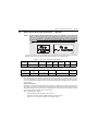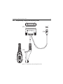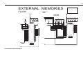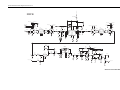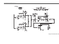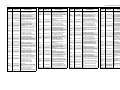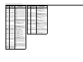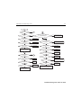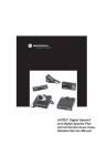
1
Foreword
This manual covers all models of the XPR series Portable Radios, unless otherwise specified. It includes all the
information necessary to maintain peak product performance and maximum working time, using levels 1 and 2
maintenance procedures. This level of service goes down to the board replacement level and is typical of some local
service centers, Motorola Authorized Dealers, self-maintained customers, and distributors.
Product Safety and RF Exposure Compliance
!
Caution
Before using this product, read the operating instructions
for safe usage contained in the Product Safety and RF
Exposure booklet enclosed with your radio.
ATTENTION!
This radio is restricted to occupational use only to satisfy FCC RF energy exposure requirements.
Before using this product, read the RF energy awareness information and operating instructions in the
Product Safety and RF Exposure booklet enclosed with your radio (Motorola Publication part number
6881095C98) to ensure compliance with RF energy exposure limits.
For a list of Motorola-approved antennas, batteries, and other accessories, visit the following web site
which lists approved accessories:http://www.motorola.com/governmentandenterprise
Computer Software Copyrights
The Motorola products described in this manual may include copyrighted Motorola computer programs stored in
semiconductor memories or other media. Laws in the United States and other countries preserve for Motorola certain
exclusive rights for copyrighted computer programs, including, but not limited to, the exclusive right to copy or reproduce in
any form the copyrighted computer program. Accordingly, any copyrighted Motorola computer programs contained in the
Motorola products described in this manual may not be copied, reproduced, modified, reverse-engineered, or distributed in
any manner without the express written permission of Motorola. Furthermore, the purchase of Motorola products shall not
be deemed to grant either directly or by implication, estoppel, or otherwise, any license under the copyrights, patents or
patent applications of Motorola, except for the normal non-exclusive license to use that arises by operation of law in the
sale of a product.
Document Copyrights
No duplication or distribution of this document or any portion thereof shall take place without the express written permission
of Motorola. No part of this manual may be reproduced, distributed, or transmitted in any form or by any means, electronic
or mechanical, for any purpose without the express written permission of Motorola.
Disclaimer
The information in this document is carefully examined, and is believed to be entirely reliable. However, no responsibility is
assumed for inaccuracies. Furthermore, Motorola reserves the right to make changes to any products herein to improve
readability, function, or design. Motorola does not assume any liability arising out of the applications or use of any product
or circuit described herein; nor does it cover any license under its patent rights nor the rights of others.
Trademarks
MOTOROLA and the Stylized M logo are registered in the US Patent & Trademark Office. All other product or service
names are the property of their respective owners.
© Motorola, Inc. 2009.
iii
Document History
The following major changes have been implemented in this manual since the previous edition:
Edition
68009273001-A
Description
Initial Release
800/900 Band information
Date
Jun. 2009
iv
Notes
v
Table of Contents
Document History .......................................................................................................... iii
Section 1
Introduction ......................................................................... 1-1
1.0 Notations Used in This Manual............................................................................ 1-1
2.0 Radio Description ................................................................................................ 1-1
Section 2
Maintenance ........................................................................ 2-1
1.0 Introduction .......................................................................................................... 2-1
2.0 Preventive Maintenance ...................................................................................... 2-1
2.1 Inspection ....................................................................................................... 2-1
2.2 Cleaning Procedures...................................................................................... 2-1
2.3 Safe Handling of CMOS and LDMOS Devices .............................................. 2-2
3.0 Repair Procedures and Techniques — General.................................................. 2-4
4.0 Notes For All Schematics and Circuit Boards...................................................... 2-6
Section 3
Test Equipment and Service Aids ..................................... 3-1
1.0 Recommended Test Equipment .......................................................................... 3-1
2.0 Service Aids......................................................................................................... 3-2
3.0 Programming, Testing and Alignment Cable ....................................................... 3-3
Section 4
Power Up Self-Test ............................................................. 4-1
1.0 Power-Up Error Codes (Display Model only)....................................................... 4-1
2.0 Operational Error Codes...................................................................................... 4-2
Section 5
Controller Information ........................................................ 5-1
1.0 General Controller Block...................................................................................... 5-1
1.1 OMAP1710 Processor (U1000)...................................................................... 5-1
1.2 Flash Memory (U2000)................................................................................... 5-2
1.3 DDR RAM (U2001)......................................................................................... 5-2
1.4 MAKO IC (U3000) .......................................................................................... 5-2
2.0 Controller Board................................................................................................... 5-2
2.1 Radio Power Distribution................................................................................ 5-2
2.2 Clocks............................................................................................................. 5-4
2.3 Serial Peripheral Interface (SPI)..................................................................... 5-5
2.4 Serial Synchronous Interface (SSI) ................................................................ 5-6
2.5 ACC_ID Interface ........................................................................................... 5-7
2.6 USB Interface ................................................................................................. 5-7
2.7 Universal Connector (Side Connector)........................................................... 5-8
vi
2.8 Keypad Module...............................................................................................5-8
2.9 Display Module ...............................................................................................5-8
2.10 Audio...............................................................................................................5-9
2.11 Troubleshooting Charts ................................................................................5-11
Troubleshooting Flow Chart for Controller (Sheet 1 of 2) .....................................5-11
Troubleshooting Flow Chart for Controller (Sheet 2 of 2) .....................................5-12
2.12 Controller Schematics ..................................................................................5-13
Complete Controller Schematic Diagram..............................................................5-13
MAKO-Controller Schematic Diagram ..................................................................5-14
Complete Controller Microprocessor Schematic Diagram ....................................5-15
Controller Memory Schematic Diagram ................................................................5-16
Controller Audio and Digital Interface Schematic Diagram...................................5-17
Controller Power Management Block Schematic Diagram (for 8478056A01) .....5-18
Controller Line Regulators for GPS Schematic Diagram ......................................5-19
Controller LCD and Speaker Interface Schematic Diagram (for 8478056A01) ....5-20
Controller UC Interface Schematic Diagram (for 8478056A01)............................5-21
Controls and Switches Schematic Diagram (for 8478056A01).............................5-22
Section 6
800/900 BAND (806–941 MHz) Information ....................... 6-1
1.0 Transmitter ...........................................................................................................6-1
1.1 General ...........................................................................................................6-1
2.0 Receiver ...............................................................................................................6-4
2.1 Receiver Front-End.........................................................................................6-4
2.2 Receiver Back-End .........................................................................................6-5
3.0 Frequency Generation Circuitry ...........................................................................6-5
3.1 Synthesizer .....................................................................................................6-6
3.2 VCO - Voltage Controlled Oscillator ...............................................................6-6
4.0 Global Positioning System (GPS) Receiver .........................................................6-7
5.0 Circuit Board/Schematic Diagrams and Parts List ...............................................6-9
Main Board Top Side PCB No. 8478056A01..........................................................6-9
Main Board Bottom Side PCB No. 8478056A01...................................................6-10
Complete Radio Schematic Diagram....................................................................6-11
Complete RF Schematic Diagram ........................................................................6-12
Complete Transmitter Schematic Diagram ...........................................................6-13
Transmitter Schematic Diagram ...........................................................................6-14
Harmonic Filter and Antenna Switch Schematic Diagram ....................................6-15
Complete Receiver Schematic Diagram ...............................................................6-16
Receiver Front End Schematic Diagram...............................................................6-17
Receiver Back End Schematic Diagram ...............................................................6-18
Complete Frequency Generating Unit Schematic Diagram ..................................6-19
Synthesizer Schematic Diagram...........................................................................6-20
Voltage Controlled Oscillator Schematic Diagram ...............................................6-21
GPS Block Schematic Diagram ............................................................................6-22
Radio Parts List (8478056A01).............................................................................6-23
vii
Section 7
Troubleshooting Charts ..................................................... 9-1
1.0 800/900 Band Troubleshooting Charts ................................................................ 9-1
Troubleshooting Flow Chart for Receiver (Sheet 1 of 2) ........................................ 9-1
Troubleshooting Flow Chart for Receiver (Sheet 2 of 2) ........................................ 9-2
Troubleshooting Flow Chart for Transmitter ........................................................... 9-3
Troubleshooting Flow Chart for Synthesizer .......................................................... 9-4
Troubleshooting Flow Chart for VCO ..................................................................... 9-5
Troubleshooting Flow Chart for GPS Receiver (Sheet 1 of 3) ............................... 9-6
Troubleshooting Flow Chart for GPS Receiver (Sheet 2 of 3) ............................... 9-7
Troubleshooting Flow Chart for GPS Receiver (Sheet 3 of 3) ............................... 9-8
Section 8
Option Board Information ................................................ 10-1
1.0 Option Board...................................................................................................... 10-1
2.0 Board Layout/Schematic for Option Board ........................................................ 10-1
2.1 Parts List for Option Board ........................................................................... 10-2
Appendix A Replacement Parts Ordering..............................................A-1
1.0
2.0
3.0
4.0
5.0
6.0
7.0
Basic Ordering Information ..................................................................................A-1
Motorola Online ...................................................................................................A-1
Mail Orders ..........................................................................................................A-1
Telephone Orders................................................................................................A-1
Fax Orders...........................................................................................................A-1
Parts Identification ...............................................................................................A-1
Product Customer Service...................................................................................A-2
Appendix B Motorola Service Centers...................................................B-1
1.0
2.0
3.0
4.0
Servicing Information ...........................................................................................B-1
Motorola Service Center ......................................................................................B-1
Motorola Canadian Technical Logistics Center ...................................................B-1
Motorola Federal Technical Center .....................................................................B-1
Glossary
..............................................................................................G-1
viii
List of Figures
List of Figures
Figure 2-1:
Figure 5-1:
Figure 5-2:
Figure 5-3:
Figure 5-4:
Figure 5-5:
Figure 5-6:
Figure 5-7:
Figure 5-8:
Figure 6-1:
Figure 6-2:
Figure 6-3:
Figure 6-4:
Figure 6-5:
Figure 8-1:
Figure 8-2:
12-Layer Circuit Board Detail Viewing ................................................................................. 2-6
Controller Block Diagram ..................................................................................................... 5-1
DC Power Distribution Block Diagram ................................................................................. 5-2
Clock Connections ............................................................................................................... 5-4
SPI Connections .................................................................................................................. 5-5
SSI Connections .................................................................................................................. 5-6
ACC_ID Interface Connections ............................................................................................ 5-7
USB Interface Connections.................................................................................................. 5-7
Audio Block Diagram ........................................................................................................... 5-9
800/900 Transmitter Block diagram ..................................................................................... 6-1
Power Control Scheme Basic Block Diagram ...................................................................... 6-3
800/900 Receiver Block Diagram ........................................................................................ 6-4
Frequency Generating Unit Block Diagram ......................................................................... 6-5
GPS Receiver Block Diagram .............................................................................................. 6-7
Option Board Layout .......................................................................................................... 10-1
Option Board Schematic .................................................................................................... 10-2
List of Tables
ix
List of Tables
Table 1-1.
Table 2-2.
Table 2-3.
Table 3-1.
Table 3-2.
Table 3-3.
Table 4-4.
Table 4-5.
Radio Frequency Ranges and Power Levels....................................................................... 1-1
Lead Free Solder Wire Part Number List ............................................................................. 2-4
Lead Free Solder Paste Part Number List ........................................................................... 2-4
Recommended Test Equipment ........................................................................................... 3-1
Service Aids ......................................................................................................................... 3-2
Pin Configuration of Side Connector.................................................................................... 3-4
Power-Up Error Codes......................................................................................................... 4-1
Operational Error Codes ...................................................................................................... 4-2
x
Related Publications
Related Publications
IMPRES Adaptive Single-Unit Charger User Manual ..................................................................6816787H01
IMPRES Adaptive Multi-Unit Charger User Manual.....................................................................6816789H01
IMPRES Adaptive Multi-Unit Charger Service Manual ................................................................ 6871357L01
Remote Speaker Microphone User Manual ................................................................................. 6871003L01
IMPRES Remote Speaker Microphone User Manual .................................................................. 6871004L01
Factory Mutual Approval Manual ................................................................................................. 6871532L01
*MOTOTRBO™ Portable User Guide CD ....................................................................................HKLN4282_
*CD consists of:
XPR™ 6300/6350 User Guide
XPR™ 6300/6350 Quick Reference Card
XPR™ 6500/6550 User Guide
XPR™ 6500/6550 Quick Reference Card
Safety Leaflet
Commercial Warranty
xi
Commercial Warranty
Limited Warranty
MOTOROLA COMMUNICATION PRODUCTS
I. What This Warranty Covers And For How Long
MOTOROLA INC. (“MOTOROLA”) warrants the MOTOROLA manufactured Communication
Products listed below (“Product”) against defects in material and workmanship under normal use and
service for a period of time from the date of purchase as scheduled below:
XPR Series Digital Portable Radios
Two (2) Years
Product Accessories (Excluding Batteries and Chargers)
One (1) Year
The portables additionally ship with a standard 1-year Repair Service Advantage (RSA) (for U.S.
customers) or 1-year Extended Warranty (for Canada customers). However, at the time of order, you
may choose to omit these warranties. For more RSA or Extended Warranty information, please refer
to the portable price pages or Motorola Online (https://businessonline.motorola.com) > Resource
Center > Services > Service Product Offerings > Repair Service Advantage or Extended Warranty.
Motorola, at its option, will at no charge either repair the Product (with new or reconditioned parts),
replace it (with a new or reconditioned Product), or refund the purchase price of the Product during
the warranty period provided it is returned in accordance with the terms of this warranty. Replaced
parts or boards are warranted for the balance of the original applicable warranty period. All replaced
parts of Product shall become the property of MOTOROLA.
This express limited warranty is extended by MOTOROLA to the original end user purchaser only
and is not assignable or transferable to any other party. This is the complete warranty for the Product
manufactured by MOTOROLA. MOTOROLA assumes no obligations or liability for additions or
modifications to this warranty unless made in writing and signed by an officer of MOTOROLA.
Unless made in a separate agreement between MOTOROLA and the original end user purchaser,
MOTOROLA does not warrant the installation, maintenance or service of the Product.
MOTOROLA cannot be responsible in any way for any ancillary equipment not furnished by
MOTOROLA which is attached to or used in connection with the Product, or for operation of the
Product with any ancillary equipment, and all such equipment is expressly excluded from this
warranty. Because each system which may use the Product is unique, MOTOROLA disclaims
liability for range, coverage, or operation of the system as a whole under this warranty.
xii
Commercial Warranty
II. General Provisions
This warranty sets forth the full extent of MOTOROLA'S responsibilities regarding the Product.
Repair, replacement or refund of the purchase price, at MOTOROLA's option, is the exclusive
remedy. THIS WARRANTY IS GIVEN IN LIEU OF ALL OTHER EXPRESS WARRANTIES. IMPLIED
WARRANTIES, INCLUDING WITHOUT LIMITATION, IMPLIED WARRANTIES OF
MERCHANTABILITY AND FITNESS FOR A PARTICULAR PURPOSE, ARE LIMITED TO THE
DURATION OF THIS LIMITED WARRANTY. IN NO EVENT SHALL MOTOROLA BE LIABLE FOR
DAMAGES IN EXCESS OF THE PURCHASE PRICE OF THE PRODUCT, FOR ANY LOSS OF
USE, LOSS OF TIME, INCONVENIENCE, COMMERCIAL LOSS, LOST PROFITS OR SAVINGS
OR OTHER INCIDENTAL, SPECIAL OR CONSEQUENTIAL DAMAGES ARISING OUT OF THE
USE OR INABILITY TO USE SUCH PRODUCT, TO THE FULL EXTENT SUCH MAY BE
DISCLAIMED BY LAW.
III. State Law Rights
SOME STATES DO NOT ALLOW THE EXCLUSION OR LIMITATION OF INCIDENTAL OR
CONSEQUENTIAL DAMAGES OR LIMITATION ON HOW LONG AN IMPLIED WARRANTY
LASTS, SO THE ABOVE LIMITATION OR EXCLUSIONS MAY NOT APPLY.
This warranty gives specific legal rights, and there may be other rights which may vary from state to
state.
IV. How To Get Warranty Service
You must provide proof of purchase (bearing the date of purchase and Product item serial number)
in order to receive warranty service and, also, deliver or send the Product item, transportation and
insurance prepaid, to an authorized warranty service location. Warranty service will be provided by
Motorola through one of its authorized warranty service locations. If you first contact the company
which sold you the Product, it can facilitate your obtaining warranty service. You can also call
Motorola at 1-800-927-2744 US/Canada.
V. What This Warranty Does Not Cover
A. Defects or damage resulting from use of the Product in other than its normal and customary
manner.
B. Defects or damage from misuse, accident, water, or neglect.
C. Defects or damage from improper testing, operation, maintenance, installation, alteration,
modification, or adjustment.
D. Breakage or damage to antennas unless caused directly by defects in material workmanship.
E. A Product subjected to unauthorized Product modifications, disassemblies or repairs (including, without limitation, the addition to the Product of non-Motorola supplied equipment) which
adversely affect performance of the Product or interfere with Motorola's normal warranty
inspection and testing of the Product to verify any warranty claim.
F.
Product which has had the serial number removed or made illegible.
G. Rechargeable batteries if:
- any of the seals on the battery enclosure of cells are broken or show evidence of tampering.
- the damage or defect is caused by charging or using the battery in equipment or service
other than the Product for which it is specified.
H. Freight costs to the repair depot.
Commercial Warranty
xiii
I.
A Product which, due to illegal or unauthorized alteration of the software/firmware in the Product, does not function in accordance with MOTOROLA’s published specifications or the FCC
type acceptance labeling in effect for the Product at the time the Product was initially distributed from MOTOROLA.
J.
Scratches or other cosmetic damage to Product surfaces that does not affect the operation of
the Product.
K. Normal and customary wear and tear.
VI. Patent And Software Provisions
MOTOROLA will defend, at its own expense, any suit brought against the end user purchaser to the
extent that it is based on a claim that the Product or parts infringe a United States patent, and
MOTOROLA will pay those costs and damages finally awarded against the end user purchaser in
any such suit which are attributable to any such claim, but such defense and payments are
conditioned on the following:
A. that MOTOROLA will be notified promptly in writing by such purchaser of any notice of such
claim;
B. that MOTOROLA will have sole control of the defense of such suit and all negotiations for its
settlement or compromise; and
C. should the Product or parts become, or in MOTOROLA's opinion be likely to become, the
subject of a claim of infringement of a United States patent, that such purchaser will permit
MOTOROLA, at its option and expense, either to procure for such purchaser the right to continue using the Product or parts or to replace or modify the same so that it becomes noninfringing or to grant such purchaser a credit for the Product or parts as depreciated and accept
its return. The depreciation will be an equal amount per year over the lifetime of the Product
or parts as established by MOTOROLA.
MOTOROLA will have no liability with respect to any claim of patent infringement which is based
upon the combination of the Product or parts furnished hereunder with software, apparatus or
devices not furnished by MOTOROLA, nor will MOTOROLA have any liability for the use of ancillary
equipment or software not furnished by MOTOROLA which is attached to or used in connection with
the Product. The foregoing states the entire liability of MOTOROLA with respect to infringement of
patents by the Product or any parts thereof.
Laws in the United States and other countries preserve for MOTOROLA certain exclusive rights for
copyrighted MOTOROLA software such as the exclusive rights to reproduce in copies and distribute
copies of such Motorola software. MOTOROLA software may be used in only the Product in which
the software was originally embodied and such software in such Product may not be replaced,
copied, distributed, modified in any way, or used to produce any derivative thereof. No other use
including, without limitation, alteration, modification, reproduction, distribution, or reverse
engineering of such MOTOROLA software or exercise of rights in such MOTOROLA software is
permitted. No license is granted by implication, estoppel or otherwise under MOTOROLA patent
rights or copyrights.
VII. Governing Law
This Warranty is governed by the laws of the State of Illinois, USA.
xiv
Battery and Charger Warranty
Battery and Charger Warranty
Workmanship Warranty
The workmanship warranty guarantees against defects in workmanship under normal use and
service.
All MOTOTRBO Batteries
Two (2) Years
IMPRES Chargers (Single-Unit and Multi-Unit, Non-Display)
Two (2) Years
IMPRES Chargers (Multi-Unit with Display)
One (1) Year
Capacity Warranty
The capacity warranty guarantees 80% of the rated capacity for the warranty duration.
Nickel Metal-Hydride (NiMH) or Lithium-Ion (Li-lon) Batteries
12 Months
IMPRES Batteries, When Used Exclusively with IMPRES
Chargers
18 Months
Section 1
INTRODUCTION
1.0
Notations Used in This Manual
Throughout the text in this publication, you will notice the use of note and caution notations. These
notations are used to emphasize that safety hazards exist, and due care must be taken and
observed.
NOTE: An operational procedure, practice, or condition that is essential to emphasize.
!
CAUTION indicates a potentially hazardous situation which, if
not avoided, might result in equipment damage.
Caution
2.0
Radio Description
The XPR series portable radios are available in the following frequency ranges and power levels.
Table 1-1. Radio Frequency Ranges and Power Levels
Frequency Band
Bandwidth
Power Level
800/900
RX/TX Talk around
851-870MHz
935-941MHz
1 Watt or 2.5 Watt
800/900
TX Trunking
806-825MHz
896-902MHz
1 Watt or 2.5 Watt
These radios are among the most sophisticated two-way radios available. They have a robust design
for radio users who need high performance, quality, and reliability in their daily communications. This
architecture provides the capability of supporting a multitude of legacy and advanced features
resulting in a more cost-effective two-way radio communications solution.
1-2
Radio Description
Notes
Section 2
MAINTENANCE
1.0
Introduction
This chapter provides details about the following
2.0
•
Preventive maintenance (inspection and cleaning).
•
Safe handling of CMOS and LDMOS devices.
•
Repair procedures and techniques
Preventive Maintenance
Periodic visual inspection and cleaning is recommended.
2.1
Inspection
Check that the external surfaces of the radio are clean, and that all external controls and switches
are functional. It is not recommended to inspect the interior electronic circuitry.
2.2
Cleaning Procedures
The following procedures describe the recommended cleaning agents and the methods to be used
when cleaning the external and internal surfaces of the radio. External surfaces include the front
cover, housing assembly and battery case. These surfaces should be cleaned whenever a periodic
visual inspection reveals the presence of smudges, grease, and/or grime.
NOTE Internal surfaces should be cleaned only when the radio is disassembled for service or
repair.
The only recommended agent for cleaning the external radio surfaces is a 0.5% solution of a mild
dishwashing detergent in water. The only factory recommended liquid for cleaning the printed circuit
boards and their components is isopropyl alcohol (100% by volume).
!
Caution
The effects of certain chemicals and their vapors can have harmful results on
certain plastics. Avoid using aerosol sprays, tuner cleaners and other
chemicals.
Cleaning External Plastic Surfaces
Apply the 0.5% detergent-water solution sparingly with a stiff, non-metallic, short-bristled brush to
work all loose dirt away from the radio. Use a soft, absorbent, lintless cloth or tissue to remove the
2-2
Preventive Maintenance
solution and dry the radio. Make sure that no water remains entrapped near the connectors, cracks,
or crevices.
Cleaning Internal Circuit Boards and Components
Isopropyl alcohol (100%) may be applied with a stiff, non-metallic, short-bristled brush to dislodge
embedded or caked materials located in hard-to-reach areas. The brush stroke should direct the
dislodged material out and away from the inside of the radio. Make sure that controls or tunable
components are not soaked with alcohol. Do not use high-pressure air to hasten the drying process
since this could cause the liquid to collect in unwanted places. After completing of the cleaning
process, use a soft, absorbent, lintless cloth to dry the area. Do not brush or apply any isopropyl
alcohol to the frame, front cover or back cover.
NOTE Always use a fresh supply of alcohol and a clean container to prevent contamination by
dissolved material (from previous usage).
2.3
Safe Handling of CMOS and LDMOS Devices
Complementary metal-oxide semiconductor (CMOS) devices are used in this family of radios, and
are susceptible to damage by electrostatic or high voltage charges. Damage can be latent, resulting
in failures occurring weeks or months later. Therefore, special precautions must be taken to prevent
device damage during disassembly, troubleshooting, and repair.
Handling precautions are mandatory for CMOS circuits and are especially important in low humidity
conditions.
Preventive Maintenance
2-3
DO NOT attempt to disassemble the radio without first referring to the following CAUTION
statement.
!
Caution
This radio contains static-sensitive devices. Do not open the radio unless you are
properly grounded. Take the following precautions when working on this unit:
• Store and transport all CMOS devices in conductive material so that
all exposed leads are shorted together. Do not insert CMOS devices
into conventional plastic “snow” trays used for storage and transportation of other semiconductor devices.
• Ground the working surface of the service bench to protect the
CMOS device. We recommend using a wrist strap, two ground
cords, a table mat, and a floor mat.
• Wear a conductive wrist strap in series with a 100k resistor to
ground. (Replacement wrist straps that connect to the bench top
covering are Motorola part number 4280385A59).
• Do not wear nylon clothing while handling CMOS devices.
• Do not insert or remove CMOS devices with power applied. Check
all power supplies used for testing CMOS devices to be certain that
there are no voltage transients present.
• When straightening CMOS pins, provide ground straps for the apparatus used.
• When soldering, use a grounded soldering iron.
• If at all possible, handle CMOS devices by the package and not by
the leads. Prior to touching the unit, touch an electrical ground to
remove any static charge that you may have accumulated. The
package and substrate may be electrically common. If so, the reaction of a discharge to the case would cause the same damage as
touching the leads.
• This radio also contain static sensitive GaAs RF switches. These
devices should be handled with the same precaution as CMOS
devices.
NOTE Replace with dust cover when the universal connector is not in use.
2-4
3.0
Repair Procedures and Techniques — General
Repair Procedures and Techniques — General
NOTE
Environmentally Preferred Products (EPP) (refer to the marking on the printed circuit
boards — examples shown below) were developed and assembled using environmentally preferred components and solder assembly techniques to comply with the European Union’s Restriction of Hazardous Substances (ROHS) Directive 2002/95/EC
and Waste Electrical and Electronic Equipment (WEEE) Directive 2002/96/EC. To
maintain product compliance and reliability, use only the Motorola specified parts in this
manual.
Any rework or repair on Environmentally Preferred Products must be done using the appropriate
lead-free solder wire and lead-free solder paste as stated in the following table:
Table 2-2. Lead Free Solder Wire Part Number List
Motorola
Part Number
Alloy
Flux Type
Flux Content
by Weight
Melting
Point
Supplier Part
number
Diameter
Weight
1088929Y01
95.5Sn/3.8Ag/0.7Cu
RMA Version
2.7-3.2%
217C
52171
0.015”
1lb spool
Table 2-3. Lead Free Solder Paste Part Number List
Motorola Part
Number
Manufacturer Part
Number
1085674C03
NC-SMQ230
Viscosity
Type
Composition & Percent Metal
900-1000KCPs
Brookfield (5rpm)
Type 3
(-325/+500)
(95.5%Sn-3.8%Ag-0.7%Cu)
89.3%
Liquid
Temperature
217°C
Parts Replacement and Substitution
When damaged parts are replaced, identical parts should be used. If the identical replacement part
is not locally available, check the parts list for the proper Motorola part number and order the part
from the nearest Motorola Radio Products and Solutions Organization (RPSO) listed in Appendix A
of this manual.
Rigid Circuit Boards
The family of radios uses bonded, multi-layer, printed circuit boards. Since the inner layers are not
accessible, some special considerations are required when soldering and unsoldering components.
The printed through holes may interconnect multiple layers of the printed circuit. Therefore, exercise
care to avoid pulling the plated circuit out of the hole.
When soldering near connector:
•
Avoid accidentally getting solder in the connector.
•
Be careful not to form solder bridges between the connector pins.
•
Examine your work closely for shorts due to solder bridges.
Repair Procedures and Techniques — General
2-5
Chip Components
Use the RLN4062 Hot-Air Repair Station for chip component replacement. Adjust the temperature
control to 370°C (700°F), and adjust the airflow to a minimum setting. Airflow can vary due to
component density.
•
To remove a chip component:
1.
Use a hot-air hand piece and position the nozzle of the hand piece approximately 0.3 cm
(1/8") above the component to be removed.
2.
Begin applying the hot air. Once the solder reflows, remove the component using a pair of
tweezers.
3.
Using a solder wick and a soldering iron or a power desoldering station, remove the excess
solder from the pads.
•
To replace a chip component using a soldering iron:
1.
Select the appropriate micro-tipped soldering iron and apply fresh solder to one of the solder
pads.
2.
Using a pair of tweezers, position the new chip component in place while heating the fresh
solder.
3.
Once solder wicks onto the new component, remove the heat from the solder.
4.
Heat the remaining pad with the soldering iron and apply solder until it wicks to the component. If necessary, touch up the first side. All solder joints should be smooth and shiny.
•
To replace a chip component using hot air:
1.
Use the hot-air hand piece and reflow the solder on the solder pads to smooth it.
2.
Apply a drop of solder paste flux to each pad.
3.
Using a pair of tweezers, position the new component in place.
4.
Position the hot-air hand piece approximately 0.3 cm (1/8”) above the component and begin
applying heat.
5.
Once the solder wicks to the component, remove the heat and inspect the repair. All joints
should be smooth and shiny.
2-6
4.0
Notes For All Schematics and Circuit Boards
Notes For All Schematics and Circuit Boards
* Component is frequency sensitive. Refer to the Electrical Parts List for value and usage.
1. Unless otherwise stated, resistances are in Ohms (k = 1000), and capacitances are in picofarads
(pF) or microfarads (µF).
2. DC voltages are measured from point indicated to chassis ground using a Motorola DC multimeter or equivalent. Transmitter measurements should be made with a 1.2 µH choke in series with
the voltage probe to prevent circuit loading.
3. Reference Designators are assigned in the following manner:
700/900 Series
=
Transmitter
000/200 Series
=
Frequency Generation
400/600 Series
=
Receiver
1000/2000/3000 Series
=
Controller
6000 Series
=
Keypad Board
8000 Series
=
GPS
9000 Series
=
Switches and User Interfaces
4. Interconnect Tie Point Legend:
UNSWB+
=
Unswitch Battery Voltage (7.5V)
SWB+
=
Switch Battery Voltage (7.5V)
R5
=
Receiver Five Volts
CLK
=
Clock
Vdda
=
Regulated 3.3 Volts (for analog)
Vddd
=
Regulated 3.3 Volts (for digital)
SYN
=
Synthesizer
DACRX
=
Digital to Analog Voltage (For Receiver Front End Filter)
VSF
=
Voltage Super Filtered (5 volts)
VR
=
Voltage Regulator
12-LAYER CIRCUIT BOARD DETAIL VIEWING
COPPER STEPS IN PROPER LAYER SEQUENCE
12-LAYER CIRCUIT BOARD DETAIL VIEWING
Solder mask
copper foil + plated
L1
Prepreg 1080x1
copper foil + plated
L2
Prepreg 1080x1
copper foil + plated
L3
PTH
1-12
L4
L5
L6
L7
L8
L9
L10
L11
L12
Buried
via
L3L10
Prepreg 1080x1
0.5 oz
CORE 4mil(2116*1)
0.5 oz
Prepreg 1080x1
0.5 oz
CORE 4mil(2116*1)
0.5 oz
Prepreg 1080x1
0.5 oz
CORE 4mil(2116*1)
0.5 oz
Prepreg 1080x1
copper foil + plated
Prepreg 1080x1
copper foil + plated
Prepreg 1080x1
copper foil + plated
Solder mask
Figure 2-1: 12-Layer Circuit Board Detail Viewing
Section 3
TEST EQUIPMENT AND SERVICE AIDS
1.0
Recommended Test Equipment
The list of equipment contained in Table 3-1 includes most of the standard test equipment required
for servicing Motorola portable radios.
Table 3-1. Recommended Test Equipment
Equipment
Characteristics
Example
Application
Service
Monitor
Can be used as a substitute for items marked with
an asterisk (*)
Aeroflex 2975
(www.aeroflex.com),
Motorola R2670, or equivalent
Frequency/deviation meter and
signal generator for wide-range
troubleshooting and alignment
Digital RMS
Multimeter *
100 µV to 300 V
5 Hz to 1 MHz
10 Mega Ohm Impedance
Fluke 179 or equivalent
(www.fluke.com)
AC/DC voltage and
current measurements. Audio
voltage measurements
RF Signal
Generator *
100 MHz to 1 GHz
-130 dBm to +10 dBm
FM Modulation 0 kHz to
10 kHz
Audio Frequency 100 Hz
to 10 kHz
Agilent N5181A
(www.agilent.com),
Ramsey RSG1000B
(www.ramseyelectronics.com), or
equivalent
Receiver measurements
Oscilloscope *
2 Channel
50 MHz Bandwidth
5 mV/div to 20 V/div
Leader LS8050
(www.leaderusa.com),
Tektronix TDS1001b
(www.tektronix.com),
or equivalent
Waveform measurements
Power Meter
and Sensor *
5% Accuracy
100 MHz to 500 MHz
50 Watts
Bird 43 Thruline Watt Meter
(www.bird-electronic.com) or
equivalent
Transmitter power output
measurements
RF Millivolt
Meter
100 mV to 3 V RF
10 kHz to 1 GHz
Boonton 92EA
(www.boonton.com) or equivalent
RF level measurements
Power Supply
0 V to 32 V
0 A to 20 A
B&K Precision 1790
(www.bkprecision.com)
or equivalent
Voltage supply
3-2
Service Aids
2.0
Service Aids
Table 3-2 lists the service aids recommended for working on the radio. While all of these items are
available from Motorola, most are standard workshop equipment items, and any equivalent item
capable of the same performance may be substituted for the item listed.
Table 3-2. Service Aids
Motorola
Part No.
Description
Application
RLN4460_
Portable Test Set
Enables connection to the audio/accessory jack.
Allows switching for radio testing.
RVN5115_
Customer Programming
Software on CD-ROM
Allows servicer to program radio parameters, tune
and troubleshoot radios.
PMKN4012_
Portable Programming Cable
This cable connects the radio to a USB port for radio
programming and data applications.
PMKN4013_
Portable Programming, Testing &
Alignment Cable
This cable connects the radio to a USB port for radio
programming, testing and alignment.
PMNN4076_
7.5V Universal Battery Eliminator
Connects to radio via battery eliminator cable.
5880348B33
DMR SMA to BNC RF Adaptor
Adapts radio’s antenna port to BNC cabling of test
equipment.
PMHN4085_
Bench Test Housing Eliminator
Interconnects radio to power supply. Provides for
troubleshooting of the radio when the housing is
removed.
NLN9839_
Vacuum Pump Kit
Allows servicer to test for leakages.
NTN4265_
Pressure Pump Kit
Allows servicer to locate leakages.
5871134M01
Connector Fitting
This connector allows the vacuum hose to be connected to the radio chassis.
3271133M01
Fitting Seal
This seal secures the connector fitting to the radio
chassis.
Programming, Testing and Alignment Cable
3.0
3-3
Programming, Testing and Alignment Cable
#25
P1
#14
#1
#13
#1
P2
P3
#1
#2
#11
#12
Figure 3-1. Programming, Testing and Alignment Cable
#4
3-4
Programming, Testing and Alignment Cable
Table 3-3. Pin Configuration of Side Connector
CONNECTION
P1
P2
Pin
Pin
Pin
1
3
VCC (5V)
3
4
DATA +
2
5
DATA -
16
6
GROUND
7
8
SPEAKER -
17
10
EXTERNAL MIC +
16
11
EXTERNAL MIC -
20
9
EXTERNAL PTT
1
7
SPEAKER +
4
P3
1
(Coax
Connector)
Function
GROUND
Section 4
POWER UP SELF-TEST
1.0
Power-Up Error Codes (Display Model only)
Upon powering up, the radio performs certain tests to determine if its basic electronics and software
are in working order. Any error detected has an associated error code that is presented on the radio
display. These error codes are intended to be used by a service technician when the radio
generates the Self Test Fail Tone. If these tests are successfully completed, the radio will generate
the Self Test Tone.
There are two classes of detectable errors, fatal and non-fatal. If it is considered as a fatal error, then
the normal radio operation will be inhibited. Fatal errors include hardware errors detected by the
microprocessor and certain memory errors. These memory errors include incorrect ROM checksum,
incorrect RAM checksum, and incorrect checksums of codeplug (Persistent Storage) blocks that
contain operating parameters. If the codeplug block operating parameters are corrupted, operation
of the unit on the proper frequency, system, and group are in question. Attempts to use this
information could provide the user with a false sense of security that others are receiving his
messages. Corrupted codeplug blocks of call IDs, or their associated aliases are considered nonfatal errors. While the user may be inconvenienced, normal communication is still possible.
Table 4-4. Power-Up Error Codes
Error Code
Description
Error Type
Corrective Action
ERROR 01/02 Call ID or associated
aliases codeplug block
checksum is wrong.
Non-Fatal
Normal communication is still possible, but the
user may be inconvenienced.
Reprogram codeplug.
ERROR 01/22 Tuning Codeplug block
checksum is wrong.
Non-Fatal
Normal communication is still possible.
FAIL 01/82
External Codeplug block
checksum is wrong.
Fatal
Reprogram codeplug.
FAIL 01/92
Secure Codeplug check- Fatal
sum error
Reprogram codeplug.
FAIL 01/A2
Tuning Codeplug block
checksum is wrong.
Fatal
Reprogram codeplug.
FAIL 01/81
ROM Checksum is
wrong.
Fatal
Reprogram FLASH Memory, then retest. If
message reoccurs, replace main board or
send radio to nearest Motorola Depot.
FAIL 01/88
Radio RAM Test Failure.
Fatal
Retest radio by turning it off and turning it on
again. If message reoccurs, replace main
board or send radio to nearest Motorola
Depot.
FAIL 01/90
or
FAIL 02/90
General hardware test
failure.
Fatal
Retest radio by turning it off and turning it on
again. If message reoccurs, replace main
board or send radio to nearest Motorola
Depot.
4-2
Operational Error Codes
Table 4-4. Power-Up Error Codes (Continued)
Error Code
Description
Error Type
Corrective Action
FAIL 02/81
DSP ROM Checksum is
wrong.
Fatal
Reprogram FLASH Memory, then retest. If
message reoccurs, replace main board or
send radio to nearest Motorola Depot.
FAIL 02/82
DSP RAM1 test failure.
Fatal
Retest radio by turning it off and turning it on
again. If message reoccurs, replace main
board or send radio to nearest Motorola
Depot.
FAIL 02/84
DSP RAM2 test failure.
Fatal
Retest radio by turning it off and turning it on
again. If message reoccurs, replace main
board or send radio to nearest Motorola
Depot.
FAIL 02/88
DSP RAM test failure.
Fatal
Retest radio by turning it off and turning it on
again. If message reoccurs, replace main
board or send radio to nearest Motorola
Depot.
FAIL 02/C0
DSP ROM Checksum is
wrong.
Fatal
Retest radio by turning it off and turning it on
again. If message reoccurs, replace main
board or send radio to nearest Motorola
Depot.
No Display
Display module is not
connected properly.
Display module is damaged.
Fatal
Check connection between main board and
display module.
Replace with new display module.
NOTE A non-display radio emits only the Self Test Fail Tone if it fails the self-test.
2.0
Operational Error Codes
During radio operation, the radio performs dynamic tests to determine if the radio is working properly.
Problems detected during these tests are presented as error codes on the radio’s display. The
presence of an error code should prompt a user that a problem exists and that a Motorola Authorized
MOTOTRBO dealer should be contacted. Use Table 4-5. to aid in understanding particular
operational error codes.
Table 4-5. Operational Error Codes
Error Code
Description
Error Type
Corrective Action
FAIL 001
Synthesizer Out-of-Lock
NON-FATAL
1. Reprogram the codeplug.
2. Refer to Detailed Service
Manual.
FAIL 002
Personality checksum or
system block error
NON-FATAL
Reprogram the codeplug.
Section 5
CONTROLLER INFORMATION
1.0
General Controller Block
The controller board is the central interface between the various subsystems of the radio. The
controller section consists of 4 main ICs. These are the OMAP1710 Host/DSP Processor, Flash, DDR
RAM memories and the MAKO Audio/Power Management chip.
Figure 5-1 shows how the controller interfaces with the RF Section and the supporting controls,
switches and display. The Controller, RF sections, volume port, frequency selection switch and the
universal connector are placed on a single “Transceiver” board. LCD Display is mounted directly to
the Transceiver board and keypad is designed on the flex. The Option Board is a separate board that
hosts the line/connections to the flex keypad. The physical interface between the Transceiver board
and keypad board is via flex through board to board connector on the option board.
B+ = 7.5V
R F S E C T IO N
SPI
SPI
SSI
MCBSP2
MPUIO
O MA P 1 710
& ME MO R Y
VDD
REF
SUPPLY
CLK
RF
LOGIC
LAYER 1
TIMER
CLOCK
PLL
DE V I C E S
MCBSP1
TUNE
LIN
REG
AUD
AMP
MIC
AMP
CODEC
MCBSP1
LCD
CTRL
SW
REG
DAC
MA K O
ADC
OPT
SEL
ON
Logic
USB
TXCVR
C ON T R OL L E R
A C C E S S OR Y
IN T E R F A C E
O P T IO N B O A R D
MCBSP1
DATA
L C D DIS P L A Y
DATA
OPT. SEL
EXT_MIC
K E YPAD
U S E R B UTTON S & K NOB S
Numeric K eys
Navigation Keys
PTT & SIDE BUTTONS
ON_OFF VOLUME
FREQ KNOB
EMERGENCY
EXT_SPK
T R A N S DU C E R S
INT_SPK
INT_MIC
Figure 5-1: Controller Block Diagram
1.1
OMAP1710 Processor (U1000)
The OMAP processor (U1000) has a dual-core architecture which incorporates a TMS320C55x DSP
core and a high-performance ARM926EJS core. The OMAP is supplied with two voltages: 1.4V for
Core and 1.8V for Peripheral and I/O Interfaces.
5-2
Controller Board
The OMAP processor controls the operation of the transmitter, receiver, synthesizer and MAKO IC. It
also uses Flash and DDR RAM, both located externally.
1.2
Flash Memory (U2000)
The Flash memory IC is a 64Mbit CMOS device. It is supplied with 1.8V. The Flash memory has its 25
address lines and 16 data lines connected to the External Interface Module (EIM) of the OMAP IC
through the EMIFS_ADDR(25:1) and EMIFS_DATA(15:0) busses. The Flash memory contains host
firmware, DSP firmware, codeplug data, and tuning values.
1.3
DDR RAM (U2001)
The Double Data Rate DRAM (DDR RAM) is 256Mb high-speed CMOS device. It is designed to
operate in 1.8V, low-power memory system. The SDRAM has 13 address lines and 16 data lines
connected to the EIM of OMAP IC through SDRAM_ADDR(12:0) and SDRAM_DATA(15:0) busses.
1.4
MAKO IC (U3000)
The MAKO IC handles DC power distribution and audio processing (i.e. audio amplification and
analog-to-digital/ digital-to-analog conversions). It contains Switching and Linear regulators, 1W audio
amplifiers, 16-bit Voice CODEC, 11-channel 10-bit A/D Converter, 10 bit D/A Converter, support
2xUSB “OTG” transceivers, One-Wire Option Detect, and GCAI ports.
2.0
Controller Board
2.1
Radio Power Distribution
RAW_B+
RF PA, RF DRIVER, ANTENNA SWITCH
KEYPAD LEDS - 8x
DISPLAY BACKLIGHT LEDS - 2x
RED & GRN LEDs, OPTION BOARD
SWB+
MOS
SW
3.6V Switcher @ 800mA
1.4V Switcher @ 800mA
OMAP CORE
MAKO DC REGULATORS
AUDIO_PA
SW1 ( 800mA @ 3.6V )
(with External FETs + Drivers)
1.2V LDO @ 0.15A
GPS RTC
2.8V LDO @ 0.1A
GPS DIG
2.8V LDO @ 0.1A
GPS RF
FET_EN
BAT_7V5
3A FUSE
BPLUS
SW2 (300mA @ 2.3V )
2.3V LDO @ 0.32A
V2 (120mA @ 1.875V )
(1.55, 1.7, 1.8, 1.875, 1.9V)
1.875V_DIG_V2
ON_OFF Switch
V3 (150mA @ 1.3V )
(1.1, 1.2, 1.3, 1.4, 1.5, 1.55, 1.6V)
IGN_X
(MECH_SW)
OMAP EIMFS & EIMFF (FLASH & SDRAM),
LCD, OMAP1710 PERIPHERAL PLUS PTT/
EMERG_PB/ RED & GRN LEDs/ FREQ SW
PULL -UPs, 32kHz SCHMITT TRIGGER CKTs,
ABACUS I/O, 12C DEVICE, RS232_USB_X
Pull Up Resistor, Trident
V4 ( 100mA @ 2.775V )
2.775V_DIG_V4
LCD, 32kHz SQUARER CKTs, LEVEL
TRANSLATOR (GPS), Trident DIG CKTs
2.9V_DIG_V6
MAKO A/D REFERENCE VOLTAGE, VOL,
HW_ID, 1-WIRE BIASING RESISTOR
2.775V_ANA_V7
TRIDENT CODE & ANALOG CKT, LNA
ABACUS CORE & DIG CKTs
3.3V_DIG_V10
GPIO1&2 PULL-UP RESISTOR, RED &
GRN LEDs, VBUS SUPPLY ENABLED
V6 ( 50mA @ 2.9V )
(2.775, 2.9V)
7.5V BATTERY
V7 ( 100mA @ 2.775V )
VSAVE
V9 ( 50mA @ 3.0V )
(2.8, 3.0, 3.3V)
SW_TYPE
V10 ( 70mA @ 3.3V )
SWB+
PGLDO3
PGLDO2
VSW5 ( 800mA @ 5.2V )
(with External FETs + Drivers)
VBUS1( 500mA @ 5.0V )
(with External Pass xistor)
5.6V LDO @ 1A
5V_ANA_VBUS1
5V_ANA_VBUS2
BAT_TYPE
VBUS2 ( 500mA @ 5.0V )
(with External Pass xistor)
5V_ANA_V8
V8 ( 25mA @ 5.0V )
SIDE ACCESSORY VBUS
1 WIRE CIRCUIT, INT, MIC BIAS, USB ESD
IC, TX PRE_DRIVER, Harmonic Filter
Antenna Switch, VCO Buffer
TRIDENT CHARGE PUMP, SF SUPPLY
(800/900VCCs), IF AMP, ABACUS CP,
BATT_DATA Biasing, USB-GPIO Switch
Figure 5-2: DC Power Distribution Block Diagram
Controller Board
5-3
Figure 5-2 illustrates the DC distribution to various ICs and devices in the radio. The power
management architecture is centered on the MAKO IC (U3000). A battery supply is routed via a 3A
fuse (F9000) which goes directly to the electronic ON/OFF control (PMOS power FET Q3003) as
RAWB+. When the radio is turned ON, MECH_SW (ON/OFF/volume control) will trigger the MAKO
FET_ENX to low thus turning ON the PMOSFET device, and SWB+ is then distributed as shown in
Figure 5-2. SWB+ will continue to support the whole board until the radio is turned OFF.
2.1.1 Voltage Regulation
• Switcher U3020
Switcher (U3020) in conjunction with the MAKO power management IC (U3000) is a highly efficient
dc-dc buck converter. External components L3020 and C3202 are needed to filter out the dc-dc
converter output. In this application, it is configured as a Pulse Skipping Mode (PSM) with maximum
output current of 600mA. It generates an accurate 3.6V output, which supplies directly to the MAKO
internal VSW2 switcher circuit as well as other MAKO internal LDOs.
• Switcher U3021
Switcher (U3021) is a highly efficient dc-dc buck converter and same as switcher U3020. It is used
solely for OMAP processor core.
• Low Drop Out (LDO) Regulator U3008
LDO regulator (U3008) is an adjustable output voltage regulator which can supply 200mA load
current. It has an excellent Ripple Rejection Ratio and Short Circuit Protection. In this application,
LDO U3008 output is 2.3V which is set by the resistor divider R3028 and R3029. It supplies directly to
MAKO internal LDOs.
• Low Drop Out (LDO) Regulator U3002
LDO regulator (U3002) is an adjustable output voltage regulator which can supply 1A load current. In
this application, LDO U3002 generates an accurate 5.6V output which is set by the resistor divider
R3017 and R3018. It supplies directly to both VBUS1 and VBUS2 supplies. Q3005 and Q3006
prevent internal voltage leakage onto VBUS_SUPPLY (U3002 pin 5).
• MAKO LDO VBUS1
VBUS1 is a voltage regulation module that can be used to provide 5V with either 50mA or 500mA
load current suited for accessory and USB supply. Q3001 and Q3002 are used to control the low
current limit (50mA) or high current limit (500mA) of Vbus1.
When USB_CONNECT is toggled LOW, the PMOSFET (Q3001) is disabled and this will limit the max
load supply to 50mA. If a high current limit is desired, i.e. USB HOST mode, USB_CONNECT is
toggled HIGH turning ON the PMOSFET (Q3001) through Q3002 inverter, and this will limit the max
load supply to 500mA.
• MAKO LDO VBUS2
VBUS2 is a voltage regulation module that can be used to provide 5V and with only 500mA load
current. This supply is used for PA Pre-driver.
• MAKO LDOs
The MAKO power management IC (U3000) provides eight more LDOs. Some LDOs are
programmable to meet the requirement of various ASIC devices. V2, V3, and V9 are programmable
via SPI while V4, V5, V6, V8, and V10 are fixed. See Figure 5-2 for details.
5-4
Controller Board
2.1.2 Power ON/OFF
The radio can be switched ON in only one condition:
1. MECH_SW turned ON
Turning the rotary switch (S9001) ON will cause MAKO (U3000) to turn ON SWB+. After application
of power to SWB+, MAKO regulators are sequenced to turn ON power to all MAKO internal blocks
and external system including OMAP processor (U1000), FLASH (U2000), SDRAM (U2001), and
radio RF section.
Radio can be turned OFF in one of the three conditions:
1. MECH_SW turned OFF
If the radio is manually turned OFF, MAKO (U3000) will start a 125ms watchdog timer. The OMAP
processor (U1000) may tickle the watchdog timer as needed to keep DC power ON as it shuts down
the radio. Once the watchdog timer expires, MAKO turns OFF the DC regulators and SWB+.
2. Low Battery
While the radio is ON, if battery voltage drops to low level threshold, OMAP processor (U1000) will
initiate a shutdown process. It will store the radio personality data to the FLASH (U2000) before
turning OFF.
3. Thermal Shutdown
Hard and Soft limits for thermal shutdown are implemented into MAKO IC (U3000). When MAKO die
temperature reaches Soft Thermal Limit (135 °C), microprocessor will be interrupted to begin
shutdown procedures. If Hard Thermal Limit (155 °C) is reached before OMAP processor (U1000)
can finish shutdown tasks, the radio will turn OFF immediately.
2.2
Clocks
Figure 5-3 illustrates the controller clocks used throughout the radio.
TRIDENT
U001
ABACUS III
U600
REF_OSC_OUT
REF_IN
FREF
AUX_DAC
16.8 MHZ
TCXO
SiRF GPS
U8000
+0.5 ppm (GPS & CPHER)
REF_CLK
RTC_XO
32.768KHZ
Y8000
RTC_XI
+20 ppm
1.4V
LOW_REF_CLK
MAKO
U3000
10K
U1006
EXT_CLK (N18)
General Pupose
TIMER
CLK32K_IN (P13)
OSC32K_IN (V13)
OMAP1710
U1000
OSC32K_OUT (AA13)
VSS_11 (Y13)
SYS_CLK_IN (Y4)
U3003
U3004
XOUT
XIN
XTAL32_IN
XTAL32_OUT
OSC_IN (Y2)
24.576MHZ
Y3001
32.768KHZ
Y3000
+30 ppm
+20 ppm
DPLL1
xN
MPU CLK
xN
DSP CLK
xN
TC CLK
12MHZ
Y1000
32.768 KHz
OSC_OUT (W3)
+20 ppm
OMAP 3.3 Core
Figure 5-3: Clock Connections
Controller Board
5-5
The OMAP processor (U1000), which consists of an ARM and DSP core, needs three clocks for
operation: a 32.768kHz square-wave, a 12MHz sine-wave, and a 16.8MHz square-wave clock.
The 16.8MHz clock source is provided from the Trident TCXO routes to a squarer-circuit (U1006) and
feed to EXT_CLK (U1000 pin N18).
The 32.768kHz clock is generated by the MAKO crystal (Y3000) oscillator, converted to a gated clock
by U3003 and U3004 circuitry. It is then directly fed to OMAP CLK32_IN (U1000 pin P13). The OMAP
processor needs the 32.768kHz to determine the input reference clock applied to OSC_IN (U1000 pin
Y2). Without this 32kHz clock, the OMAP will potentially program all the wrong dividers for USB and
UART booting. External pull-up on OSC32K_IN (U1000 pin V13) and grounding both OSC32K_OUT
(pin AA13) and VSS_11 (pin Y13) indicates that an external 32kHz clock is used.
The 12MHz sine-wave is the main system reference clock for the OMAP which all the internal clocks
are derived from.
The 24.576MHz crystal (Y3001) oscillator is the reference clock for MAKO CODEC and SSI clock. `
2.3
Serial Peripheral Interface (SPI)
Figure 5-4 illustrates the controller SPI used throughout the radio.
1.8V
OMAP1710
U1000
1.8V
HPD SPI
TRIDENT
U001
SPI_CLK
SPI_DW
SPI_CLK
SPIF.SCK (U19)
SPI_MOSI
SPIF.DOUT (W21)
MMC1 SPI
SPI.CLK (M14)
MMC.CMD (P11)
SPI_MISO
SPI_DR
SPIF.DIN (U18)
THK_CE
CEX
SPI.CS2 (P20)
GPIO_44 (P15)
1.8V
SPI.CS1 (P19)
PC
ABACUS III
U600
PD
DOUTB
ABACUS3_CE
PE
GPIO_9 (Y8)
1.8V
SPI.RDY (R18)
SPI_CLK
MAKO
U3000
SPI_DO
SPI.CS3 (P18)
SPI_DI
SPI_CS
MAKO_CE
GPIO_58 (R11)
R3023
47K
Figure 5-4: SPI Connections
The OMAP processor (U1000) has two SPI busses that it uses to communicate with the various
peripheral IC’s. The first is the High Performance Data (HPD) SPI bus and the second is the multimedia card (MMC) SPI.
5-6
Controller Board
The HPD SPI is a synchronous serial bus made up of four lines, SPI_CLK, SPI_MOSI, SPI_MISO,
and chip select. The SPI_CLK line is used to control the speed of the data to/from the peripheral IC’s
and the OMAP processor. This clock can be adjusted to different speed based on the IC’s
specification.
HPD SPI module is used to interface to Trident (U001), Abacus III (U600), and the MAKO (U3000).
This interface operates at 1.875V logic level. SPI_MOSI, or commonly known as TRANSMIT Data, is
a data string from OMAP while SPI_MISO or RECEIVE Data is data string to the OMAP.
The MMC SPI is not used in portable radio.
2.4
Serial Synchronous Interface (SSI)
Figure 5-5 illustrates the controller SSI used in the radio controller design.
1.8V
OMAP1710
U1000
1.8V
DMCS
TRIDENT
U001
GPIO_2 (D15)
McBSP2.CLKX (Y6)
TX_CLK
TX_DATA
McBSP2.DX (AA5)
TX_FSYNC
McBSP2.FSX (W7)
1.8V
ABACUS III
U600
McBSP2
CLKOUT
McBSP2.CLKR (V7)
DOUTA
McBSP2.DR (P10)
FS
McBSP2.FSR (W6)
SYNCB
McBSP3
McBSP3.CLKX (N14)
McBSP3.FSX (AA17)
GPIO_40 (W15)
McBSP3.DX (P14)
1.8V
McBSP1
VC_DCLK
MAKO
U3000
McBSP1.FSX (H15)
VC_FSYNC
VC_RX
McBSP1.DX (H18)
McBSP1.DR (H20)
VC_TX
OPTION
BOARD I/F
J9001
McBSP3.DR (T19)
McBSP1.CLKX (G21)
CLK
FSYNC
VC_RX
VC_TX
R3010
10K
Figure 5-5: SSI Connections
The OMAP processor (U1000) has a total of three SSI or multi-channel buffer serial ports (McBSP)
modules that are used to directly interface to the CODECs in the Trident, Abacus, and MAKO, as well
as command/ data connections to the Option Board, and between Tx and Rx radios within a
Repeater.
As shown in Figure 5-5, McBSP1 is a 4-wire bus and interface to the MAKO CODEC as well as the
Option Board. McBSP2 is 6-wire bus; 3-wire dedicated to the Trident Tx audio and the other 3-wire to
Abacus Rx audio. McBSP3 is a 4-wire bus, and used primarily to interface between Tx and Rx radios
within a Repeater.
Controller Board
2.5
5-7
ACC_ID Interface
Smart accessories use the Accessory ID (ACC_ID) Interface to help the radio determine which smart
accessory, if any, are attached to the radio. Figure 5-6 illustrate the ACC_ID connections used within
the radio.
5V
2.9V
1.875V
2.9V
5V
R3300
R3304
R3031
Vref1
MAKO
U3000
OMAP1710
U1000
ACC_ID (P9)
HDQ (N20)
Vref2
SCL1
SCL2
SDA1
SDA2
ACC_ID_UP (L7)
2-BitTranslator
U3009
Figure 5-6: ACC_ID Interface Connections
2.6
USB Interface
The OMAP processor (U1000) supports two USB ports. The radio makes use of one USB port to
communicate with smart accessories, and connection to a host computer for radio programming via
CPS and tuning via Tuner Tool.
Note:
The USB ports are designed to support Motorola accessories only and will not support third
party “Plug-n-Play” USB devices.
Figure 5-7 shows the details of the HSSI connections within the radio.
Mako
VBUS SUPPLY
OMAP 1710
VBus1_Sens (E12)
USB1_TXEN (W16)
USB1_DAT (W14)
USB1_SE0 (R13)
USB1_OE (B08)
USB1_DAT_TXD (C08)
USB1_SE0 (D08)
3/6 Wire
IF and
SPI
Registers
Vbus1
Monitor
USB_INT (L15)
VBus1_Cmd (C14)
VBus1 (H10)
USB1
Transceiver
R3103 + R3102
Q3000
VBus
DP (N6)
D+
DM (P7)
D-
USB_INTX (C10)
Figure 5-7: USB Interface Connections
The OMAP processor USB host controller communicates with accessories at either 1.5 Mbps or 12
Mbps data rates depending on the accessory. The USB port can be used as a host or a device.
5-8
Controller Board
In the portable radio, only one of the two MAKO USB transceivers is used to provide the physical
layer signaling for the USB port. The transceiver generates and receives the DP and DM differential
signals of the port. The MAKO transceiver interfaces to the OMAP processor through a three-wire
interface consisting of two bi-directional signals (SE0 and DAT), and one uni-directional signal
(TXEN). The MAKO also includes a Vbus monitor that senses the connection or removal of a device
and determines whether or not to supply current to that device via Q3000 up to a high current limit of
500mA.
The USB host/device mode assignment is determined when a user attaches a USB device to the port.
The accessory contains information about what the USB mode assignment should be, this
information is sent to the radio via the ACC_ID. See section 2.5 on page 5-7 for more details on the
ACC_ID implementation. When configured as a host, VBUS is turned ON by MAKO and set to high
current limit, when configured as a device, VBUS will be shut OFF and the external host supplies the
VBUS power.
2.7
Universal Connector (Side Connector)
The universal connector is located on the side of the radio. It is the external port of interface used for
programming and interfacing to external accessories. The universal connector is connected to the
main board via a flex through option board. This radio UC is a newly defined Motorola accessory port
that contains audio, digital I/O, serial interfaces, and accessory supply lines; and is similar in function
to Motorola’s legacy microphone connectors. The multiplexing of these functions is handled by
circuitry internal to the MAKO (U3000).
The UC includes 2 serial interfaces: an USB port and an ACC_ID interface. The USB port can be
used as either a device (radio is device) or as a host (radio is host). When configured as a device, the
radio can be programmed using the MOTOTRBO CPS or tuned using the Tuner software. When
configured as a host, various smart accessories can be used with the radio. See section 2.6 on page
5-7 for more information on the USB interface.
The ACC_ID interface is used by accessories to provide the radio with information needed to
configure the interface for that accessory. See section 2.5 on page 5-7 for more information on the
ACC_ID interface.
Note:
2.8
The USB port is designed to support Motorola accessories only and will not support third
part “Plug-n-Play” USB devices.
Keypad Module
The keypad module is connected to the main board through option board. This unit is not considered
field-repairable. The keypad interface is a standard pulsed 4 row by 4 column configuration controlled
directly by the OMAP processor (U1000). Each of the 4 column output lines is toggled high in
sequence and the 4 row input lines are monitored to detect if a button has been pressed. The OMAP
processor then decodes which button was pressed using the appropriate column and row stimulus
and response information.
2.9
Display Module
This display is Film-compensated Super Twisted Nematic (FSTN), 132x34 pixel dot matrix with
transflective mode and yellow-green LEDs backlighting Liquid Crystal Display (LCD) module custom
to Motorola.
This display module is constructed of glass by sandwiched with polarizers, TAB (Tape Automated
Bonding) IC driver, LED backlighting, display control circuitry flex with 16-lines receptacle connector
connected to the main board display connector (P9000). The LED and backlights are controlled via
serial connection with OMAP processor (U1000). The serial interface consists of clock, data, and chip
select lines that are connected directly from the OMAP processor.
Controller Board
2.10
5-9
Audio
V02_O(1.875V) for OMAP
V06(2.9V) for Patriot
MIC BIAS
MIC BIAS
L OGIC_VDD
The audio circuitry consists of both analog and digital audio paths. Figure 5-8 shows the basic block
diagram of the audio interconnections.
MAKO
VC_TX3V
INT_MIC_P
INT_MIC_P
INT_MIC_M
INT_MIC_M
1.0uF
ADC
1.0uF
VC_TX
DIN
10k
EXT_MIC_M
0.1uF
MICSEL
EXT_MIC_P
TX
Base-Band
Processor
VC_DCLK
CLK
VCM1
VC_FSYNC
VC_OUT_P
SYNC
DAC
VC_RX
UCM_SS
DOUT
RX
VC_OUT_M
0.1uF
PA_IN_P
Rf
15nF
Cf
C2
PA_IN_M
Rf
270 Ohm
EXT_SPKR_P
PA
LSPKext
EXT_SPKR_M
INT_SPKR_P
LSPKint
PA
INT_SPKR_M
Figure 5-8: Audio Block Diagram
2.10.1 Receive Audio
The receive audio data comes from the ABACUS III IC (U600) to the OMAP McBSP2 pin. The DSP
decodes the data and sends it out through SSI lines to MAKO SSI pin. The SSI bus is comprised of
four lines: clock, frame sync, Rx data, and Tx data. These four lines provide data to the MAKO
(U3000) using a packet frame structure consisting of four slots. The actual audio data is transferred to
the MAKO in the first slot of each frame using 16-bit pulse-code modulated PCM audio. The MAKO
codec filters and converts the digital data into an analog audio signal, and this signal is sent to a
programmable gain amplifier. The analog audio circuitry routes the audio to the internal or external
port.
5-10
Controller Board
2.10.2 Transmit Audio
Transmit audio can be sourced from either internal or external microphone path. Both the internal and
external microphone carries a 5V bias through a resistor to MAKO MIC_BIAS pin. The MAKO,
through SPI, selects the appropriate microphone path to route to the necessary gain stages and
converter that will send 16-bit PCM audio to the OMAP for signal processing via the SSI bus.
The transmit gain stages in the MAKO is calibrated based on an 8mV input under standard test
conditions. The microphone sensitivity is programmable through the use of CPS.
5-11
2.11
Troubleshooting Charts
MCU
Power Up
Alert Tone
OK?
YES
Read Radio
OK?
NO
Check USB
circuitry and
setup
YES
NO
Volume
knob
function?
Reprogram
correct data
NO
Check volume
knob circuitry
NO
Replace
Speaker
YES
Speaker
OK?
YES
Int & Ext
Spkr short to
Gnd?
YES
Check Speaker
circuitry, if no problem,
replace MAKO
NO
Termination
short
together?
YES
NO
Spkr contact
voltage
=3V?
NO
YES
A
Troubleshooting Flow Chart for Controller
(Sheet 1 of 2)
5-12
A
YES
NO
MAKO
regulator o/p
programmed?
YES
1.4V at
R1020?
NO
Check regulator
U3201
NO
Check TRIDENT
16.8MHz circuitry
YES
16.8MHz at
C1032?
YES
NO
C1019
=12MHz?
YES
R1048=
32.768MHz?
NO
YES
C1019=
12MHz?
YES
Replace
U3003
YES
Replace
Y3000
NO
YES
NO
Replace
OMAP
C3001
=32.768KHz?
C3000
=32.768KHz?
NO
Replace
Y1000
Troubleshooting Flow Chart for Controller
(Sheet 2 of 2)
Replace
MAKO
Controller Schematics
Controller Schematics
5V_ANA_VBUS2
5V_ANA_VBUS2
KEYPAD_COL0
KEYPAD_COL1
KEYPAD_COL2
KEYPAD_COL3
KEYPAD_COL4
KEYPAD_ROW0
KEYPAD_ROW1
KEYPAD_ROW2
KEYPAD_ROW3
KEYPAD_ROW4
KEYPAD_COL0
KEYPAD_COL1
KEYPAD_COL2
KEYPAD_COL3
KEYPAD_COL4
KEYPAD_ROW0
KEYPAD_ROW1
KEYPAD_ROW2
KEYPAD_ROW3
KEYPAD_ROW4
EXT_MICEXT_MIC+
EXT_MICEXT_MIC+
GPS_BOOT
JTAG_TDO
JTAG_TMS
JTAG_TDI
JTAG_TCK
JTAG_NTRST
JTAG_NEMU1
JTAG_NEMU0
JTAG_RTCK
OPT_GPIO_1
OPT_GPIO_2
OPT_GPIO_1
OPT_GPIO_2
ONE_WIRE_1
USB1_DP
USB1_DM
THK_CE
ABACUS3_CE
SPI_CLK
SPI_MOSI
SPI_MISO
5V_ANA_V8
2.775V_ANA_V7
2.775V_DIG_V4
1.875V_DIG_V2
5V_ANA_VBUS2
RAWB+
SWB+
2.9V_DIG_V6
VBUS1
VBUS1
5V_ANA_VBUS2
1.875V_DIG_V2
2.775V_DIG_V4
2.9V_DIG_V6
2.775V_ANA_V7
5V_ANA_V8
3.6V_DIG_VSW1
3.3V_DIG_V10
SWB+
16_8MHZ
GPS_nWAKEUP
GPS_RFPWRUP
GPS_TX
GPS_RX
GPS_ON_OFF
GPS_nRESET
MAKO_FSYNC
MAKO_DCLK
MAKO_TX
MAKO_RX
USB1_DP
USB1_DM
PA_TEMP
EXT_SPKREXT_SPKR+
OPTA_SEL0
OPTA_SEL1
OPTA_SEL2
DEEP_SLEEP
DMCS
VA_SW
ANT_EN
LOCK_DETECT
SYNCB
TX_DAC
THK_CE
ABACUS3_CE
SPI_CLK
SPI_MOSI
SPI_MISO
TX_CLK
TX_DATA
TX_FSYNC
TX_CLK
TX_DATA
TX_FSYNC
RX_CLK
RX_DATA
RX_FSYNC
RX_CLK
RX_DATA
RX_FSYNC
DEEP_SLEEP
DMCS
VA_SW
ANT_EN
LOCK_DETECT
SYNCB
TX_DAC
DEEP_SLEEP
DMCS
VA_SW
ANT_EN
LOCK_DETECT
SYNCB
TX_DAC
RF
GPS_ANT
MAKO_FSYNC
MAKO_DCLK
MAKO_TX
MAKO_RX
OPTA_SEL0
OPTA_SEL1
OPTA_SEL2
CONTROLLER
OPT_SSI_SYNC
ONE_WIRE_1
RX_CLK
RX_DATA
RX_FSYNC
PTT
INT_SPKRINT_SPKR+
EXT_SPKREXT_SPKR+
TX_CLK
TX_DATA
TX_FSYNC
INT_MICINT_MIC+
INT_SPKRINT_SPKR+
THK_CE
ABACUS3_CE
SPI_CLK
SPI_MOSI
SPI_MISO
OPT_SSI_SYNC
PTT
INT_MICINT_MIC+
SW8
SW4
SW2
SW1
EMERG_PB
BATT_DATA
2.8V_DIG_GPS
2.8V_RF_GPS
1.5V_GPS_RTC
VOL
MECH_SW
VOL
MECH_SW
BL_EN
DISPLAY_CE
DISPLAY_CMD
DISPLAY_DATA0
DISPLAY_DATA1
DISPLAY_DATA2
DISPLAY_DATA3
DISPLAY_DATA4
DISPLAY_DATA5
DISPLAY_DATA6
DISPLAY_DATA7
SW8
SW4
SW2
SW1
EMERG_PB
BATT_DATA
2.8V_DIG_GPS
2.8V_RF_GPS
1.5V_GPS_RTC
RAWB+
GREEN_LED
RED_LED
BL_EN
DISPLAY_CE
DISPLAY_CMD
DISPLAY_DATA0
DISPLAY_DATA1
DISPLAY_DATA2
DISPLAY_DATA3
DISPLAY_DATA4
DISPLAY_DATA5
DISPLAY_DATA6
DISPLAY_DATA7
3.3V_DIG_V10
1.875V_DIG_V2
2.775V_DIG_V4
2.775V_ANA_V7
2.775V_ANA_V7
5V_ANA_V8
RAWB+
GREEN_LED
RED_LED
2.12
5-13
RESET_OUT
PA_TEMP
GPS_ANT
PA_TEMP
16_8MHZ
GPS_nWAKEUP
GPS_RFPWRUP
GPS_TX
GPS_RX
GPS_ON_OFF
GPS_nRESET
16_8MHZ
16_8MHz_GPS
16_8MHz_GPS
GPS_BOOT
JTAG_TDO
JTAG_TMS
JTAG_TDI
JTAG_TCK
JTAG_NTRST
JTAG_NEMU1
JTAG_NEMU0
JTAG_RTCK
RESET_OUT
RESET_OUT
RESET_OUT
Complete Controller Schematic Diagram
5-14
Controller Schematics
GREEN_LED
KEYPAD_ROW0
KEYPAD_ROW1
KEYPAD_ROW2
KEYPAD_ROW3
KEYPAD_ROW4
KEYPAD_COL0
KEYPAD_COL1
KEYPAD_COL2
KEYPAD_COL3
KEYPAD_COL4
SW1
SW2
SW4
SW8
BL_EN
1.875V_DIG_V2
2.775V_DIG_V4
3.3V_DIG_V10
VBUS1
5V_ANA_VBUS2
2.9V_DIG_V6
2.775V_ANA_V7
5V_ANA_V8
2.8V_DIG_GPS
2.8V_RF_GPS
SWB+
1.5V_GPS_RTC
RAWB+
OPT_GPIO2
OPT_GPIO3
OPT_GPIO0
OPTA_SEL0
OPTA_SEL1
OPTA_SEL2
ONE_WIRE_1
MAKO_INT
MAKO_OPT_INT
MAKO_AD_TRIGGER
OPTA_SEL0
OPTA_SEL1
OPTA_SEL2
MAKO_TX
MAKO_RX
MAKO_DCLK
MAKO_FSYNC
MAKO_TX
MAKO_RX
MAKO_DCLK
MAKO_FSYNC
MAKO_INT
MAKO_OPT_INT
MAKO_AD_TRIGGER
MAKO_INT
MAKO_OPT_INT
MAKO_AD_TRIGGER
GPIO_3
DIR_CTRL
SERIAL_CLK
SERIAL_DATA
LED_CS
DISPLAY_CS
MORPH_DISPLAY_CMD
MAKO_OPT_GPIO0
MAKO_OPT_GPIO3
MAKO_OPT_GPIO2
I2C_DATA
I2C_CLK
1_WIRE_SEL
GPIO_30
GPIO_31
GPIO_32
GPIO_33
GP5_8
1.5V_GPS_RTC
RAWB+
VBUS1
5V_ANA_VBUS2
2.9V_DIG_V6
2.775V_ANA_V7
5V_ANA_V8
2.8V_DIG_GPS
2.8V_RF_GPS
SWB+
MAKO_TX
MAKO_RX
MAKO_DCLK
MAKO_FSYNC
SPI_CLK
SPI_MOSI
SPI_MISO
MAKO_CE
OMAP_CORE_LTC
1.55V_DIG_V3
1.875V_DIG_V2
2.775V_DIG_V4
3.3V_DIG_V10
2.8V_DIG_GPS
GPIO_45
MCBSP3_DX
MCBSP3_DR
MCBSP3_FSX
KEYPAD_ROW0
KEYPAD_ROW1
KEYPAD_ROW2
KEYPAD_ROW3
KEYPAD_ROW4 / GP5_6 ARMIO_15
KEYPAD_COL0
KEYPAD_COL1
KEYPAD_COL2
KEYPAD_COL3
KEYPAD_COL4 / PUBLIC_ADD_MIC_ENA GPIO_27
EMERG_PB
OMAP_CORE_LTC
1.55V_DIG_V3
SW1 / VOL_A
SW2 / VOL_B
SW4 / MONITOR
SW8 / CHANNEL_ACT
MECH_SW
EMERG_PB
ONE_WIRE_1
SPI_CLK
SPI_MOSI
SPI_MISO
MAKO_CE
BATT_DATA
MECH_SW
OMAP_CORE_LTC
1.55V_DIG_V3
1.875V_DIG_V2
2.775V_DIG_V4
3.3V_DIG_V10
BL_EN / GP5_7 ARMIO_3
BATT_DATA
MAKO_OPT_GPIO2
MAKO_OPT_GPIO3
MAKO_OPT_GPIO0
12C_CLK
12C_DATA
1_WIRE_SEL
R1100
0
DNP
SPI_CLK
SPI_MOSI
SPI_MISO
ABACUS3_CE
THK_CE
SPI_CLK
SPI_MOSI
SPI_MISO
ABACUS3_CE
THK_CE
RED_LED / RX_ATTN_1 GPIO_15
GREEN_LED / PA_ENABLE GPIO_60
GATED_32KHZ_OMAP
GPS_nWAKEUP
GPS_SHUTDOWN
GPS_TX
GPS_RX
GPS_ON_OFF
GPS_nRESET
GPS_BOOT
GPS_nWAKEUP
GPS_RFPWRUP
MAKO-Controller Schematic Diagram
GPS_TX
GPS_RX
GPS_ON_OFF
GPS_nRESET
GPS_BOOT
GPS_nWAKEUP
GPS_SHUTDOWN
ONE_WIRE_UP
POR
RS232_TX
RS232_RX
MAKO_GPIO_TX
MAKO_GPIO_RX
ARMIO_2
ONE_WIRE_UP
POR
OPT_GPIO_1
OPT_GPIO_2
GATED_32KHZ_OMAP
RS232_TX
RS232_RX
OPT_GPIO_1
OPT_GPIO_2
MMP_GPIO1_INPUT
MMP_GPIO2_INPUT
ONE_WIRE_UP
POR
USB_INT
RX_CLK
RX_DATA
RX_FSYNC
TX_CLK
TX_DATA
TX_FSYNC
DEEP_SLEEP
DMCS
ADAPT_SW
LOCK_DETECT
ANT_EN
SYNCB
16_8MHZ
GPS_SHUTDOWN
GPS_RFPWRUP
GPS_nWAKEUP
RS232_TX
RS232_RX
USB1_TXEN
USB1_DAT
USB1_SE0
JTAG_RTCK
JTAG_TMS
JTAG_TDI
JTAG_NEMU0
JTAG_NEMU1
JTAG_TDO
JTAG_NTRST
JTAG_TCK
USB1_TXEN
USB1_DAT
USB1_SE0
USB0_TXEN
USB0_DAT
USB0_SE0
USB_INT
JTAG_RTCK
JTAG_TMS
JTAG_TDI
JTAG_NEMU0
JTAG_NEMU1
JTAG_TDO
JTAG_NTRST
JTAG_TCK
VA_SW
EXT_SPKREXT_SPKR+
INT_SPKRINT_SPKR+
DISPLAY_CE
DISPLAY_CMD
DISPLAY_DATA0
DISPLAY_DATA1
DISPLAY_DATA2
DISPLAY_DATA3
DISPLAY_DATA4
DISPLAY_DATA5
DISPLAY_DATA6
DISPLAY_DATA7
OPT_SSI_SYNC
DISPLAY_CE
DISPLAY_CMD
DISPLAY_DATA0
DISPLAY_DATA1
DISPLAY_DATA2
DISPLAY_DATA3
DISPLAY_DATA4
DISPLAY_DATA5
DISPLAY_DATA6
DISPLAY_DATA7
INT_MICINT_MIC+
EXT_MICEXT_MIC+
MICROCONTROLLER
USB2_VP
USB2_VM
USB2_RCV
USB2_SUSPEND
USB2_TXEN
USB2_DAT
USB2_SE0
USB1_TXEN
USB1_DAT
USB1_SE0
USB0_TXEN
USB0_DAT
USB0_SE0
USB_INT
16_8MHZ
INT_MICINT_MIC+
EXT_MICEXT_MIC+
MAKO
AUDIO_PA_ENA
EXT_MIC_ENA
GATED_32KHZ_OMAP
VOL
PA_TEMP
MAKO_FSYNC
TX_DAC
VOL
PA_TEMP
EXT_SPKREXT_SPKR+
INT_SPKRINT_SPKR+
To Option Board
TX_DAC
USB1_DP
USB1_DM
MAKO_TX
MAKO_RX
MAKO_DCLK
MAKO_CE
USB1_DP
USB1_DM
PTT
RESET_OUT
RX_CLK
RX_DATA
RX_FSYNC
TX_CLK
TX_DATA
TX_FSYNC
DEEP_SLEEP
DMCS
LOCK_DETECT
ANT_EN
SYNCB
RED_LED
PTT
RESET_OUT
Controller Schematics
5-15
2.775V_DIG_V4
1.875V
R1055
10K
DNP
1.875V
1_WIRE_SEL
AUDIO_PA_ENA
(MORPH ONLY)
ARMIO_2
DECOUPLING CAPACITORS
LARGEST REF
R1034
10K
C1044
R1072
U1009
C1000 C1001 C1002 C1003 C1013 C1015 C1011 C1031
51pF 0.10uF 0.10uF 51pF 0.10uF0.10uF 51pF 0.10uF
OMAP_CORE
LDO_FILTER
TP_MAKO_TX
R1054
4.7K
R1053
4.7K
0
R1061
15
14
13
12
11
10
9
8
7
6
5
4
3
2
1
0
N3
C12
D12
D13
C11
C13
D11
D14
C10
D8
C4
C7
D5
D7
C5
C6
D6
J18
J19
J14
K18
K19
K15
K14
L19
L18
L15
M19
M20
N21
N19
N18
N20
W8
Y8
M15
P19
P20
P18
M14
R19
R18
T20
T19
V8
N15
U19
V16
W17
AA17
R13
W11
W10
V10
R11
ABACUS3 SSI
TX_FSYNC
TX_DATA
TX_CLK
RX_FSYNC
RX_DATA
RX_CLK
1.875V
2
FLASH
R1006
10K
A9
A3
E2
CVDD2
CVDD2_1
CVDD2_2
CVDD3_1
CVDD3_2
CVDD3_3
CVDD3_4
CVDD4
B13
B20
J21
R20
J1
Y21
W12
A11
A15
Y20
Y9
M2
AA3
CVDDA
CVDD_RTC
CVDD_DLL
CVDD_1
CVDD_2
CVDD_3
CVDD_4
CVDD1
LCD_PIXEL_15
LCD_PIXEL_14
LCD_PIXEL_13
LCD_PIXEL_12
LCD_PIXEL_11
LCD_PIXEL_10
LCD_PIXEL_9
LCD_PIXEL_8
LCD_PIXEL_7
LCD_PIXEL_6
LCD_PIXEL_5
LCD_PIXEL_4
LCD_PIXEL_3
LCD_PIXEL_2
LCD_PIXEL_1
LCD_PIXEL_0
KBC_5
KBC_4
KBC_3
KBC_2
KBC_1
KBC_0
CLK_EX_CAM
LOW_STATE_5
UART3_RX
I2C_SCL
TDO
UWIRE_SDI
UWIRE_SDO
CLK_S_UWIRE
Z_STATE_3
Z_STATE_2
MCBSP1_DX
1
2
3
4
0
5
3
FLASH_CTL(5:0)
D15
C16
A17
G13
B17
C17
D16
D17
C18
B19
A20
H13
G14
C19
B21
D18
G19
C21
E18
D19
D20
F18
H19
M18
L14
T18
AA19
U18
W21
V19
N14
P15
H18
DISPLAY_DATA7
DISPLAY_DATA6
DISPLAY_DATA5
DISPLAY_DATA4
DISPLAY_DATA3
DISPLAY_DATA2
DISPLAY_DATA1
DISPLAY_DATA0
DISPLAY_CE
DISPLAY_CMD
DISPLAY
(Used as KEYPAD_COL4 for NEO
GPIO_27 and Public Add Mic for MORPHEUS)
KEYPAD_COL3
KEYPAD_COL2
KEYPAD COLUMN
KEYPAD_COL1
KEYPAD_COL0
1
TX_RAMP
MORPH_DISPLAY_CMD (MORPH ONLY)
SPI_CLK
SPI_MISO
SPI_MOSI
THK_CE
ABACUS3_CE
SPI
MAKO_CE
R1036
10K
1.875V
2.8V_DIG_GPS
C1020
18pF
2.775V_DIG_V4
4.7K
R1063
0
DNP
E1062
BK1005HM471
RESET_OUT
1.875V
R1005
MAKO_OPT_INT
C1029
0.10uF
C1028
0.10uF
GPS_BOOT_LS
USB#2
NOT USED
B3
A1
A2
A3
A4
U1005
TXB0104ZXUR
OE
B1 C1
A1
B2 C2
A2
B3 C3
A3
B4 C4
1.875V
A4 GND
B4
GPS_TX_LS
GPS_RX_LS
USB_INT
USB1_SE0
USB1_TXEN
USB1_DAT
USB0_SE0
USB0_DAT
USB0_TXEN
USB2_SE0
R1065
0
USB2_DAT
I2C
USB2_VP
(Temporary used for Option Board SSI Sync pin)
USB2_SUSPEND
C1019
18pF
R1046
0
DNP
FDATA_15
FDATA_14
FDATA_13
FDATA_12
FDATA_11
FDATA_10
FDATA_9
FDATA_8
FDATA_7
FDATA_6
FDATA_5
FDATA_4
FDATA_3
FDATA_2
FDATA_1
FDATA_0
USB2_VM
1
HOT1
2 GND1
4
GND2
HOT2
16_8MHZ
( BUFFERRED 16.8 FROM TOMAHAWK )
FLASH_WAIT
FLASH_CLK
EMIFS_DATA(15:0)
EMIFS_ADD(25:1)
Y1000
CX3225SB
12MHz
C1032
.01uF
V3
T4
U3
U1
P8
T3
T2
R4
R3
R2
P7
P4
P2
N7
N2
N4
USB2_RCV
R1026
47K
16.8MHz Squarer
GND
3 A2
C1033
0.10uF
5
VCC
1 A1
1.875V
Y2 4
Y1 6
U1006
NL27WZU04
15
14
13
12
11
10
9
8
7
6
5
4
3
2
1
0
LCD_VSYNC B18
LCD_HSYNC C20
LCD_AC B15
CLK_P_LCD C15
B5
B7
A13
B16
A21
F20
K20
R21
W20
AA21
Y13
AA7
Y3
AA1
U2
N1
K2
G1
B1
SDRAM_ADD(12:0)
12
11
10
9
8
7
6
5
4
3
2
1
0
B2
VCCA B1
VCCB
TOMAHAWK SSI
H11
H9
H10
B8
B12
G9
G11
G12
B9
G10
A1
B6
B2
A2
SDRAM_CTL(8:0)
7
8
0
1
2
3
4
5
6
RTCK
MCSI2_DOUT
MMC_CMD
CLK_MMC
RTC_ON_NOFF
Z_STATE_1
RTC_WAKE_INT
RESET_MODE
RST_OUT
R1072
0
I2C_CLK
I2C_DATA
C1045
47pF
R1041
LEVEL TRANSLATORS
Y17
W9
P11
V11
Y12
W16
W13
P12
AA20
(MORPH ONLY) GP5_8
1K
SADD_13
SADD_12
SADD_11
SADD_10
SADD_9
SADD_8
SADD_7
SADD_6
SADD_5
SADD_4
SADD_3
SADD_2
SADD_1
SADD_0
USB2_TXEN
RS232_TX
E5 RESERVED
RS232_RX
RS232
R1001
10K
VSS_1
VSS_2
VSS_3
VSS_4
VSS_5
VSS_6
VSS_7
VSS_8
VSS_9
VSS_10
VSS_11
VSS_12
VSS_13
VSS_14
VSS_15
VSS_16
VSS_17
VSS_18
VSS_19
FADV
EN_F_BE_0
EN_F_BE_1
GPIO_62
F_CS1
F_CS2
F_CS3
EN_F_OE
F_RP
EN_F_WE
F_WP
USB0_SE0
USB0_DAT
EN_USB_PUEN
CLK_B_UART2
LOW_STATE_3
LOW_STATE_4
OMAP_CORE
W15
Y15
P14
W14
V15
AA9
V9
R10
P10
V2
V13
AA13
AA5
V5
Y2
W3
AA15
Y14
W7
V7
Y6
W6
H8
H7
D10
C8
B4
C3
B3
LDO_FILTER
L4
L3
M8
M7
M3
R1013 0
M4
DNP
N8
0 U4
R1014
W1
W2
V4
R8
P9
W4
Y4
V6
W5
OPT_GPIO_1
OPT_GPIO_2
SYNCB
MAKO_AD_TRIGGER
V12 DVDDRTC
1.875V
R1028
0
CLK_SD
R1045
10K
FADD_1
FADD_2
FADD_3
FADD_4
FADD_5
FADD_6
FADD_7
FADD_8
FADD_9
FADD_10
FADD_11
FADD_12
FADD_13
FADD_14
FADD_15
FADD_16
FADD_17
FADD_18
FADD_19
FADD_20
FADD_21
FADD_22
FADD_23
FADD_24
FADD_25
KEYPAD ROW KEYPAD_ROW2
KEYPAD_ROW1
KEYPAD_ROW0
BOOT FROM CS0
CVDDA
C1044
0.10uF
DDR RAM
EN_WE_
SDRAM
SDRAM_RAS
SDRAM_DQMU
SDRAM_DQML
SDRAM_CAS
SBANK_1
SBANK_0
U1000
OMAP1710
J8
D3
C1
E4
D2
F4
E3
J7
F3
G4
G3
G2
K8
H4
H3
K7
J2
J4
J3
F2
L8
K4
K3
L7
E1
(Used as KEYPAD_ROW4 for NEO, GP5_6 for MORPH) ARMIO_15
KEYPAD_ROW3
V20 I2C_SDA
J15 CLK_L_CAM
C9
MAKO_INT
CLKX_SD
CLK32K_IN
EN_SDCKE
CLKX_MCBSP1
CLK_MCSI2
CLKS_MCBSP1
MCBSP1_FSX
PWRON_RESET
F_CS1U
OMAP_CORE
F_CS2U
SDDQS_H
1.875V
SDDQS_L
CS_SDRAM
KBR_4
KBR_3
CVDDA VDD_DLL
KBR_2
KBR_1
DVDD2
KBR_0
MCBSP1_DR
BFAIL
CONF
TDI
TMS
TCK
TRST
MPU_BOOT
L1 NC
MPU_RST
A19 DVDD1_1
UART1_CTS
E21 DVDD1_2
UART2_CTS
U21 DVDD1_3
UART1_RX
Y16 DVDD1_4
UART2_RX
L21 DVDD1_5
CLK_B_REQ
AA2 DVDD2_1
CLK_B
Y7 DVDD2_2
CLK_MCSI1
AA11 DVDD2_3
MCSI1_DOUT
MCSI1_DIN
A5 DVDD4_1
MCSI2_DIN
A7 DVDD4_2
MCSI2_SYNC
B10 DVDD4_3
CLK_M_REQ
B14
DVDD4_4
MCBSP2_DR
FRDY
R1 DVDD5_1
OSC32K_IN
H2 DVDD5_2
OSC32K_OUT
C2 DVDD5_3
MCBSP2_DX
CLK_M
OSC1_IN
OSC1_OUT
LOW_STATE_1
LOW_STATE_2
MCBSP2_FSX
CLKR_MCBSP2
CLKX_MCBSP2
MCBSP2_FSR
1
2
3
4
5
6
7
8
9
10
11
12
13
14
15
16
17
18
19
20
21
22
23
24
25
1
D9
P13
H12
G21
Y10
G20
H15
R12
Y1
P3
C14
D4
G8
E19
E20
H14
F19
G18
H20
W19
V18
Y19
V17
W18
Y18
J20
U20
R14
Y5
V14
R9
( RESET CIRCUIT PROVIDED BY MAKO) POR
MAKO_GPIO_RX
MAKO_GPIO_TX
1.875V
C1016
0.10uF
SDRAM_CLK_EN
SDRAM_CLKX
SDRAM_DATA(15:0)
SDRAM_CLK
CLK_F
SDATA_15
SDATA_14
SDATA_13
SDATA_12
SDATA_11
SDATA_10
SDATA_9
SDATA_8
SDATA_7
SDATA_6
SDATA_5
SDATA_4
SDATA_3
SDATA_2
SDATA_1
SDATA_0
CAM_D_7
CAM_D_6
CAM_D_5
CAM_D_4
CAM_D_3
CAM_D_2
CAM_D_1
CAM_D_0
CAM_VS
CAM_HS
CAM_RSTZ
GPIO_15
GPIO_14
GPIO_13
GPIO_12
GPIO_11
GPIO_9
GPIO_8
GPIO_7
GPIO_6
GPIO_4
GPIO_3
GPIO_2
GPIO_1
GPIO_0
MPUIO_5
MPUIO_4
MPUIO_3
MPUIO_2
MPUIO_1
EMU0
EMU1
MCSI1_SYNC
CLK32K_OUT
MMC_DAT3
MMC_DAT2
MMC_DAT1
MMC_DAT0
TP_POR
R1048
0
R1027
10K
DNP
BOOT FROM CS3
R1060
10
VDD_DLL
C1012
0.10uF
LOCK_DETECT
ANT_EN
RF CONTROLS
DMCS
DEEP_SLEEP
SDRAM_CS
OPTION SELECT (FROM MAKO )
MAKO_OPT_GPIO0
MAKO_OPT_GPIO3
MAKO_OPT_GPIO2
(FROM MAKO) GATED_32KHZ_OMAP
R1000
10
R1019
5.1
FREQ SWITCH
GPIO_33 (Used as SW8 for NEO, Channel Activity for MORPH)
GPIO_32 (Used as SW4 for NEO, Monitor for MORPH)
GPIO_31 (Used as SW2 for NEO, Volume B for MORPH)
GPIO_30 (Used as SW1 for NEO, Volume A for MORPH)
EXT_MIC_ENA
(MORPH ONLY)
OMAP_CORE
DVDD2
C1017
1.0uF OMAP_CORE
C1030
18pF
C1004 C1005 C1006 C1007 C1014 C1010 C1009 C1008
51pF 0.10uF 0.10uF 51pF 0.10uF0.10uF 0.10uF 51pF
DELETED REF
MAKO_RX
MAKO_DCLK
MAKO_FSYNC
MAKO_TX
MAKO SSI
1.875V
OMAP_CORE
Y1001
R1035
0
DNP
PLACE FOR GP
DEVICE FAST BOOT
1
TP_MAKO_DCLK
1
TP_MAKO_FSYNC
1
TP_MAKO_RX
1
1
1
1
1
1
1
1
1
2.775V_DIG_V4
JTAG_NTRST
JTAG_TCK
JTAG_TMS
JTAG_TDI
JTAG_NEMU0
JTAG_NEMU1
JTAG_TDO
JTAG_RTCK
TP_RTCK
TP_TDO
TP_NEMU1
TP_NEMU0
TP_TDI
TP_TMS
TP_TCK
TP_NTRST
JTAG
GP DEVICE CONFIG
1.875V
TP030
DVDD2
DIR_CTRL
(Directional pin for McBSP3 FSX and CLK)
R1023
0
1.875V_DIG_V2
(Used as BL_EN for NEO, GP5_7 for MORPH)
ARMIO_3
1.875V
R1017
10K
PLACED FOR
MORPHEUS ONY
PTT
C1018 51pF R1025 10K
1.875V
GPIO_3
(Green LED for NEO SHIFT_REG_CE for MORPH)
R1021
0
GPS
GPS_nWAKEUP_LS
GPS_SHUTDOWN
GPS_BOOT_LS
GPS_nRESET_LS
GPS_TX_LS
GPS_RX_LS
GPS_ON_OFF_LS
1.875V_DIG_V2
OMAP_CORE
SERIAL FLASH SPI
LED_CS
SERIAL_CLK
DISPLAY_CS
SERIAL_DATA
OMAP_CORE_LTC
MCBSP3_DX
MCBSP3_FSX
MCBSP3_DR
GPIO_45
(Emergency Button)
MCBSP3
CYPHER SSI
R1020
0
GPIO_60 (PA_ENABLE for MORPH)
GPIO_15
(Used as RED_LED for NEO, RX_ATTN_1 for MORPH)
L1_TIMER
ONE_WIRE_UP
OMAP1710
GPS_nRESET_LS
R1069
0
GPS_ON_OFF_LS
R1067
12K
GPS_BOOT
GPS_TX
GPS_RX
R1070
10K
GPS_nRESET
GPS_ON_OFF
GPS_nWAKEUP
GPS_nWAKEUP_LS
R1068
24K
USB#0
USB#1
USB#0 RESERVED FOR MORPHEUS
( INTERFACE WITH MAKO )
Complete Controller Microprocessor Schematic Diagram
5-16
Controller Schematics
EXTERNAL MEMORIES
FLASH
1.875V_DIG_V2
LARGEST REF
C2007
R2013
U2001
1.875V_DIG_V2
1.875V_DIG_V2
1.875V_DIG_V2
DDR
R2004
0
R2011
0
SDRAM_CLK
SDRAM_CLKX
1.875V_DIG_V2
SDRAM_CLK_EN
1.875V_DIG_V2
R2010
10K
C2007
0.10uF
1.875V_DIG_V2
EN_F2_OE
DU7
EN_WE
DU8
EN_WP
DQ0
E5
LATCH_EN
G1
1
F1
2
E1
3
D1
4
B1
5
C1
6
F2
7
E2
8
F6
9
D7
10
E7
11
B8
12
C8
13
D8
14
F7
15
E8
16
F8
17
D2
18
B2
19
B3
20
E6
21
B7
22
C7
23
C3
24
D3
25
DQ1
ADV
DQ2
A0
DQ3
A1
DQ4
A2
DQ5
A3
DQ6
Intel Strata 32MB
5
A4
A5
A6
A7
A8
DQ7
DQ8
DQ9
DQ10
DQ11
A9
DQ12
A10
DQ13
A11
DQ14
A12
DQ15
A13
A14
RFU1
A15
RFU2
A16
RFU3
A17
RFU4
A18
RFU5
A19
RFU6
A20
RFU7
A21
RFU8
A22
RFU9
A23
RFU10
A24
RFU11
RFU12
Controller Memory Schematic Diagram
NC
NC
NC
NC
0
4
G7
1
G8
6
G9
5
H7
2
H8
3
H9
H3
1
G3
2
H4
3
7
0
J9
J5
4
8
1
K7
G5
5
2
K8
J6
6
3
K2
H7
7
4
K3
J8
G2
8
5
J1
J3
9
6
J2
G4
10
7
J3
J4
11
8
H1
H5
12
9
J7
G6
13
10
H2
H6
14
11
H3
J7
15
12
F2
F8
C2
C5
D5
D6
E3
F3
H1
J1
K2
K3
K4
K5
NC
NC
NC
NC
SDRAM_ADD(12:0)
NC
NC
NC
NC
NC
NC
NC
VSS8
K8
NC
NC
C2009
2.2uF
C2008
2.2uF
U2001
MT46H16M16LF
E9
VDDQ5
VDDQ4
B1
D1
C9
VDDQ3
VDDQ1
VDDQ2
F9
A7
K9
VDD3
CK
UDQS
LDQS
CK*
EN_CKE
0
NC
H2
VDD1
A9
NC
SDRAM_DATA(15:0)
EMIFS_DATA(15:0)
G3
G1
L8
VSS7
VSS5
VSS6
L7
L6
VSS4
L5
VSS3
L2
VSS2
L1
B4
C4
EMIFS_ADD(25:1)
VSS1
RFU13
M8
G2
0
DQ0
WE
DQ1
CAS
DQ2
RAS
DQ3
CS
DQ4
DQ5
BA0
DQ6
BA1
DQ7
A0
DQ8
A1
DQ9
A2
DQ10
A3
DQ11
A4
DQ12
A5
DQ13
A6
A7
A8
A9
DQ14
DQ15
NC1
NC2
A10_AP
A11
A12
UDM
LDM
VSSQ5
E4
M7
0
R2015
VSSQ4
F5
WRITE_PROTECT
DU6
M2
C2004
51pF
E1
WRITE_EN
4
EN_F1_OE
M1
R2014
D9
3
DU5
SDRAM_CTL(8:0)
NC
VSSQ3
OUTPUT_EN
DU4
EN_F2_CE
A8
NC
VSSQ2
H8
1
EN_F1_CE
A7
VSSQ1
J2
DU3
A2
B9
G8
EN_RST
A1
C1
NC
DU2
C2005
.01uF
Micron 32MB
K1
CE
DU1
CLK
FLASH_WAIT
VSS3
0
F4
G7
C2006
0.10uF
R2003
1K
DNP
A3
C6
RESET
R2009
10K
DNP
SDRAM_CS
WAIT
2
R2008
10K
DNP
A1
K6
L4
VCC4
B6
VCC2
VCC1
VCC3
L3
B5
VPP
K7
J8
D4
VCCQ3
VCCQ2
VCCQ1
FLASH_CLK
FLASH_CTL(5:0)
R2007
10K
DNP
R2002
1K
DNP
R2013
10K
DNP
U2000
PF48F4000P0ZBQ0
R2006
10K
DNP
VSS2
R2012
10K
R2000
10K
R2005
10K
DNP
VDD2
C2003
0.10uF
VSS1
C2002
0.10uF
F1
C2001
.01uF
K1
C2000
51pF
E2
E8
A8
0
B7
1
B8
2
C7
3
C8
4
D7
5
D8
6
E7
7
E3
8
D2
9
D3
10
C2
11
C3
12
B2
13
B3
14
A2
15
F3
F7
Controller Schematics
5-17
220pF
1.875V_DIG_V2
MAKO_TX
MAKO_RX
NC
NC
USB1_TXEN
A6
D8
A9
USB0_TXEN
B9
USB0_DAT
C9
USB0_SE0
E9
USB_INT
MAKO USB
N3
C8
USB1_SE0
R3036
10K
A7
B8
USB1_DAT
R3031
51K
M4
A10
NC
MAKO UART
RS232_TX
NC
RS232_RX
NC
B10
C10
P2
J5
C7
A8
L5
MAKO ONE WIRE
NC
R3032
8.2K
ONE_WIRE_UP
MMP_GPIO1_INPUT
NC
NC
NC
R3034
8.2K
MAKO OPTION SEL
MMP_GPIO2_INPUT
NC
MAKO_OPT_GPIO0
NC
R3035
15K
MAKO_OPT_GPIO2
R3500
N2
820
C12
E11
D10
F10
C11
G10
D11
MAKO_OPT_GPIO3
B12
MAKO_OPT_INT
0
L7
K6
M3
R3033
15K
R3501
N8
R3056
0
R3037
820
5V_ANA_VBUS2
5V_ANA_V8
SPI_CS
U3000-2
DIGITAL_BLOCK
SPI_DI
SPI_DO
VC_DCLK
VC_FSYNC
C3062
0.10uF
VC_TX
R3053
22K
VC_TX3V
R3054
22K
VC_RX
UCM_SS
LOGIC_VDD
A1
USB1_OE
B1
USB1_DAT_TXD
USB1_SE0
D2
USB2_OE_RCV_RTS
C2
USB2_DAT_VP
USB2_SE0_VM_RXD
UART2_TXD
USB1_DP
UART2_RXD_OD
USB1_DM
CTS_X
USB2_DP
USB_INTX
USB2_DM
USB_CONNECT
RXDIN_3V
SB96_BUS_BUSY
TXDO_BDI_UP_3V
SB96_BDO_KF_5V
BOOT_NORM_X
RS232_USB_X
ONE_WIRE_1
APCO
ONE_WIRE_2
SB96D_BDO_KF_3V
ONE_WIRE_BATT
TXDO_BDI_5V
ONE_WIRE_UP
TXDO_BDI_ENC_3V
RXDIN_5V
RTS_FILLSEN_5V
RXDIN_ENC_3V
RTS_FILLSEN_3V
CTS_CABLE_DET_5V
BUSY_IN
OPTA_SEL0
BUSY_OUT
OPTA_SEL1
CABLE_DET_3V
OPTA_SEL2
OPT_GPIO0
OPTA_SEL3
OPT_GPIO1
OPTB_SEL0
OPT_GPIO2
OPTB_SEL1
OPT_GPIO3
OPTB_SEL2
OPTION_INTX
OPTB_SEL3
NO1
COM1
NO2
COM2
U3007
TS5A23166
IN1
IN2
N6
P8
L6
N13
N9
P9
M8
L8
M10
N12
R3305
200K
B2
C1
C3026
0.10uF
R3301
4.7K
P7
N7
5V_ANA_VBUS2
B7
SPI_CLK
2.9V_DIG_V6
D7
USB1_DM
3.3V_DIG_V10
R3300
10K
C3025
0.10uF
NC
R3304
2.2K
NC
2
E7
MAKO_DCLK
MAKO_FSYNC
USB1_DP
USB_CONNECT
7
SPI_MISO
24
BBP_SYNC
NC
NC
3
4
NC
BATT_DATA
NC
VREF2
C6
24
R3021
VREF1
1.875V_DIG_V2
B6
SPI_MOSI
R3020
EN
SCL1
SCL2
SDA1
SDA2
8
6
ONE_WIRE_1
5
GND
D6
MAKO_CE
MAKO SSI
E6
BBP_CLK
1
SPI_CLK
B5
2.9V_DIG_V6
NC
MAKO SPI
A5
5V_ANA_V8
NC
A2
47K
V_POS
10K
R3023
GND
10K
R3010
D1
C3213
R3061
M11
P13
P10
NC
OPTA_SEL1
M9
OPTA_SEL2
N10
P11
K8
P12
N11
U3010
PCA9306
OPTA_SEL0
K7
NC
NC
R3098
3.3K
NC
NC
DNP
C3045
10uF
K1
.033uF
J2
C3048
INT_MIC-
R3011
J1
.033uF
R3027
C3049
EXT_MIC+
C3050
H3
270
R3026
.033uF
C3011
EXT_MIC-
0.10uF J3
C3036
2.2K
.015uF
.033uF
H2
270
E3
C3095
0.10uF
E1
G3
C3094
R3012
270
G2
0.10uF
F1
C3080
1.0uF
DNP
F2
H1
G1
H4
INT_SPKR
C3097
E3031
BLM18BD601SN1
33pF
C3098
E3032
BLM18BD601SN1
33pF
C3035
C3800
0.1uF
R3055
100K
0.10uF
INT_SPKR+
0.10uF
IF2
R3800
10
ADC_VREF
INT_MIC_P
ATOD_0
INT_MIC_M
ATOD_1
EXT_MIC_P
ATOD_2
EXT_MIC_M
VCM1
VC_OUT_P
ATOD_3
U3000-3
PA_CODEC_A2D_BLOCK
ATOD_4
ATOD_5
VC_OUT_M
ATOD_6
BPLUS
ATOD_7
PA_BPLUS
ATOD_8
100pF
M12
N14
2.9V_DIG_V6
M13
HW_ID0
L11
HW_ID1
M14
HW_ID2
L12
L13
PA_TEMP
K11
VOL
K12
K13
PA_IN_M
PA_IN_P
INT_SPKR_P
FE_TUNE1
INT_SPKR_M
FE_TUNE2
EXT_SPKR_P
PWR_CTRL
EXT_SPKR_M
SCAN_EN
VCM2
TEST
VREF
VFUSE
L3
M2
N1
NC
NC
R3005
0
DNP
TX_DAC
C4
A3
E8
R3060
2K
R3007
0
DNP
R3009
4.7K
R3025
100
R3004
10K
C3034
A4
E3030
BLM18BD601SN1
MIC_BIAS
100pF
C3037
R3006
10K
R3008
12K
C3999
.01uF
INT_SPKRHW_ID
HW_ID2
C3047
INT_MIC+
VMES
TX_RX
C3038
2.9V_DIG_V6
K2
L10
2.9V_DIG_V6
L2
R3013
R3014
NC
AD_TRIG
HW_ID1
A11
HW_ID0
B11
MAKO_AD_TRIGGER
2.9V_DIG_V6
2K
C3500
10uF
2.2K
5V_ANA_VBUS2
D3000
C3100
33pF
EXT_SPKR-
SWB+
33pF
VSAVE
C3099
E3033
BLM18BD601SN1
RAWB+
EXT_SPKR+
Controller Audio and Digital Interface Schematic Diagram
5-18
Controller Schematics
L3004
560nH
B3
B3
OUT
C3085
3300pF
C3087
82pF
1
C3200
0.10uF
C3201
10uF
7
3
NC
8
NC
NC
NC
NC
NC
NC
R3074
1K
A1
A14
P1
P14
M5
B14
Q3003
8
7
6
3
2
1
C3002
0.1uF
C3003
2.2uF
C3004
2.2uF
4
C3093
2.2uF
C3051
100pF
R3050
100K
C3005
1000pF
R3075 NC
NC
10K
VSAVE
MECH_SW
POR
CX-101F
Y3001 16-54MHz
NC
MAKO_INT
HOT1
C3205
680pF
C3061
20pF
R3201
62K
R3028
51.1K
R3029
41.2K
NC
C3083
0.10uF
NC
NC
NC
NC
NC
NC
C3015
100pF
1
1.875V_DIG_V2
1.55V_DIG_V3
2.775V_DIG_V4
2.9V_DIG_V6
2.775V_ANA_V7
3V_ANA_V9
3.6V_DIG_VSW1
3.3V_DIG_V10
VOUT
2
FB
6
NP
4
VCONT
3
VIN
C3016
2.2uF
U3008
TK11100CSC
C3017
.01uF
C3018
2.2uF
R3102
2
R3103
0.7
SWB+
5V_ANA_V8
Q3001
1
Q3000
GND1
GND2
GND3
GND4
GND5
GND6
GND7
GND8
GND9
GND1
NC
3.6V_DIG_VSW1
R3200
220K
NC
NC
NC
NC
R3101
100K
3
2
4
Q3002
VBUS1
C3039
P5
M7
J4
G5
K9
L4
D14
H5
D9
4
C3060
20pF
1
2
HOT2
GND2
3
ITH
4.7uF
R1
OUT
USB_CONNECT
IN
R3030
0.2
GND
4
R2
1
2
3
Q3010
5V_ANA_VBUS2
1.55V_DIG_V3
2.9V_DIG_V6
5V_ANA_VBUS2
5V_ANA_V8
3.3V_DIG_V10
U3002
LP8340
5
VOUT
4
ADJ
3
2
4
R3017
178K
1
2.775V_DIG_V4
C3081
4.7uF
DNP
Q3005
1.875V_DIG_V2
2.775V_DIG_V4
R3100
47K
5V_ANA_V8
C3090
10uF
Controller Power Management Block Schematic Diagram (for 8478056A01)
C3074
1.0uF
R1
OUT
IN
R2
GND
C3067
1.0uF
3V_ANA_V9
C3028
2.2uF
3.3V_DIG_V10
C3024
1.0uF
5V_ANA_V8
C3031
1.0uF
2.775V_ANA_V7
C3079
4.7uF
2.9V_DIG_V6
C3019
1.0uF
5V_ANA_VBUS2
C3014
2.2uF
2.775V_DIG_V4
1.55V_DIG_V3
1.875V_DIG_V2
Q3006
C3010
2.2uF
3.3V_DIG_V10
R3018
51K
GND2
7
GND1
2
1.875V_DIG_V2
2.775V_ANA_V7
SW
1
5
2
VIN
U3021
LTC1877
OMAP_CORE_LTC
L3021
10uH
SYNC
VFB
C3209
22uF
PLLLPF
ITH
C3211
20pF
R3202
220K
R3203
300K
C3204
20pF
1
5
B1
C1
F3
C2
D1
D2
D3
B2
G4
E2
F4
E4
B3
B4
C5
F5
D5
A12
A13
D4
M1
VFB
PLLLPF
RUN
C3203
.01uF
GND
C3000
13pF
C3212
220pF
C3202
68uF
5
VSAVE
C3001
13pF
5
SYNC
4
Y3000
XTAL 32.768KHz
1
SW
2
L3020
10uH
2
3
NC1
NC2
NC3
NC4
NC5
NC6
SWB+
SWB+
RAWB+
RAWB+
2
RUN
C3088
100pF
C3
A2
G13
G12
H11
J11
G14
H13
F14
H12
H14
J12
K14
J14
J13
L14
D13
F13
E14
E13
G11
F12
N4
P4
N5
P3
P6
L1
J10
M6
L9
K3
K4
B13
E12
C14
H10
F11
C13
D12
U3020
LTC1877
4
2
PGLDO2
PGLDO3
SW1_VDD
SW1_VDDHV
SW1_VSEN_BUK
SW1_VSEN_BST
SW1_SUMCOMP_DL
SW1_DH
SW1_PHASE
SW1_VOUT
SW1_GND
U3000-1
SW2_VCC
PWR_MNGR_BLOCK
SW2_VCCS
SW2_LX
SW2_VOUT
SW2_GND
SW5_VDD
SW5_VDDHV
SW5_VSENSE
XTAL32_OUT
SW5_SUMCOMP
XTAL32_IN
SW5_PHASE
BAT_RTC
SW5_VOUT
VSAVE
V02_O
BAT_7V5
V03_O
BAT_3V6
V04_O
REG_3V6
V06_O
BAT_TYPE
V07_O
HV_BG
V09_O
FET_ENX
V10_I
EMERG_PB
V10_O
MECH_SW
V10_GND
SW_TYPE
V08_I
IGN_X
V08_O
RESETX
VBUS_SUPPLY
GATED_32K_CLK
VBUS1_SENS
INT_X
VBUS1_CMD
XOUT
VBUS1
XIN
VBUS2_SENS
TCXO_SEL_16_24
VBUS2_CMD
TCXO_IN
VBUS2
6
8
MAKO_SW1_VDD
U3004
NL17SZ14
3
1
U3003-2
LMC6035ITLX
R3071
220K
IN
3
GATED_32KHZ_OMAP
4
1
4
R3070
220K
2
A3
C3207
10uF
7
6
C3
C3206
0.10uF
C3805
0.22uF
VIN
A1
SWB+
A2
B1
C1
MAKO_SW1_VDD
B1
C3084
0.22uF
L3022
560nH
C3208
0.22uF
GND
SWB+
5
C2
VCC
C3065
1uF
C3063
0.10uF
U3003-1
LMC6035ITLX
C3070
10pF
SWB+
L3003
560nH
1.875V_DIG_V2
GND
NC
2.775V_DIG_V4
R3073
2MEG
GND
R3072
2MEG
2.775V_DIG_V4
1
VIN1
6
VIN2
3
NC
SWB+
NC
C3091
10uF
C3210
.01uF
Controller Schematics
5-19
E3700
IDCTR
1
3.6V_DIG_VSW1
E3701
IDCTR
U3700
TPS79228
1
2
3
OUT
EN
BYPASS
1
5
2
2.8V_RF_GPS
4
GND
GPS_RFPWRUP
IN
C3701
.01uF
2
R3700
1K
C3700
1.0uF
1
C3702
2.2uF
2
R3702
30.9K
C3704
27pF
E3703
IDCTR
3
1
2
5
OUT
IN
BYPASS
FB
2
E3702
IDCTR
EN
C3703
1.0uF
1
6
4
GND
1
R3701
10K
1
2
GPS_nWAKEUP
2
2.8V_DIG_GPS
1
U3701
TPS79101
C3705
.01uF
C3706
470pF
C3707
2.2uF
2
R3703
24.3K
1.875V_DIG_V2
GPS_SHUTDOWN
R3704
10K
U3006
LP3990
A2
2
B2
VEN
VOUT
B1
1
2
1.5V_GPS_RTC
VIN
GND
1
E3705
IDCTR
A1
E3704
IDCTR
C3101
1.0uF
C3102
1.0uF
Controller Line Regulators for GPS Schematic Diagram
5-20
Controller Schematics
DISPLAY B2B 16 PINS CONNECTOR (2887818K02)
DISPLAY_DATA0_SW
R9000
DISPLAY_DATA1_SW
R9001
DISPLAY_DATA2_SW
R9002
1K
B2B_DISPLAY_DATA2
DISPLAY_DATA3_SW
R9003
1K
B2B_DISPLAY_DATA3
DISPLAY_DATA0
1K
B2B_DISPLAY_DATA0
1K
B2B_DISPLAY_DATA1
DISPLAY_DATA1
DISPLAY_DATA2
DISPLAY_DATA3
DISPLAY_DATA4_SW
R9004
DISPLAY_DATA5_SW
R9005
DISPLAY_DATA6_SW
R9006
DISPLAY_DATA7_SW
R9007
DISPLAY_DATA4
DISPLAY_DATA5
B2B_DISPLAY_DATA4
1K
1K
B2B_DISPLAY_DATA5
1K
B2B_DISPLAY_DATA6
1K
B2B_DISPLAY_DATA7
DISPLAY_DATA6
DISPLAY_DATA7
RESET_OUT
BL_EN
C9000
51pF
C9001
51pF
C9002
51pF
C9003
51pF
C9004
51pF
C9005
51pF
C9006
51pF
P9000-1
DISPLAY_DATA0
P9000-2
DISPLAY_DATA1
P9000-3
DISPLAY_DATA2
P9000-4
DISPLAY_DATA3
P9000-5
DISPLAY_DATA4
INTERNAL SPEAKER CONTACT
INT_SPKR+_TOP
1
INT_SPKR-_TOP
P9000-6
DISPLAY_DATA5
P9000-7
DISPLAY_DATA6
P9000-8
DISPLAY_DATA7
DNP
M9003
E9006
DNP
BLM18BD601SN1
1
DNP
M9004
E9007
DNP
BLM18BD601SN1
C9067
51pF
DNP
C9068
51pF
DNP
VR9015
10.0V
DNP
VR9016
10.0V
DNP
C9007
51pF
INT_SPKR_P_SW
INT_SPKR+
INT_SPKR+
1
INT_SPKR-
1
M9005
RESET_OUT_SW
P9000-9
RESET_OUT
RESET_OUT
INT_SPKR_M_SW
INT_SPKR-
DISPLAY_CE_SW
P9000-10
DISPLAY_CE
P9000-11
DISPLAY_CMD
P9000-12
BL_EN
1.875V_DIG_V2
P9000-13
1.875V_DIG_V2
2.775V_DIG_V4
P9000-14
2.775V_DIG_V4
SWB+
P9000-15
SWB+
P9000-16
GND
DISPLAY_CE
DISPLAY_CMD_SW
DISPLAY_CMD
BL_EN_SW
BL_EN
C9008
51pF
C9009
51pF
C9010
51pF
C9011
51pF
C9012
51pF
C9013
51pF
C9061
51pF
C9014
51pF
2.775V_DIG_V4_SW
2.775V_DIG_V4
2.775V_DIG_V4
1.875V_DIG_V2_SW
1.875V_DIG_V2
1.875V_DIG_V2
SWB_P_SW
SWB+
SWB+
VBUS1_SW
VBUS1
VBUS1
Largest reference designator
3.3V_DIG_V10
R9018
Q9003
M9007
C9068
E9007
J9001
VR9018
FL9000
P9000
D9000
L9008
3.3V_DIG_V10_SW
3.3V_DIG_V10
2.9V_DIG_V6_SW
2.9V_DIG_V6
2.9V_DIG_V6
5V_ANA_VBUS2_SW
5V_ANA_VBUS2
5V_ANA_VBUS2
S9002
Controller LCD and Speaker Interface Schematic Diagram (for 8478056A01)
C9062
51pF
VR9017
10.0V
VR9018
10.0V
M9006
Controller Schematics
5-21
OPT-Trans B2B 40 PINS CONNECTOR (0970312L02)
KEYPAD_ROW0_SW
BL_EN
J9001-9
KEYPAD_ROW0
KEYPAD_ROW0
KEYPAD_ROW1
J9001-10
KEYPAD_ROW1
J9001-11
KEYPAD_ROW2
J9001-12
KEYPAD_ROW3
J9001-13
KEYPAD_ROW4
INT_MIC_P_SW
270nH
INT_MIC_M_SW
L9008
270nH
INT_MIC+
KEYPAD_ROW2_SW
KEYPAD_ROW2
KEYPAD_ROW3_SW
INT_MIC-
KEYPAD_ROW3
J9001-23
BL_EN
J9001-22
INT_MIC+
J9001-21
INT_MIC-
L9007
KEYPAD_ROW1_SW
KEYPAD_ROW4_SW
OPT_INT_MIC_P
K1
C9044
51pF
U8003
BLM18EG221SN1
KEYPAD_COL0_SW
DLP11SN201HL2
KEYPAD_COL0
KEYPAD_COL1_SW
USB1_DP_SW
KEYPAD_COL1
J9001-16
KEYPAD_COL1
2 P1
USB1_DP
KEYPAD_COL2_SW
USB1_DM_SW
KEYPAD_COL2
J9001-17
KEYPAD_COL2
J9001-18
KEYPAD_COL3
J9001-19
KEYPAD_COL4
USB1_DM
K2
1
VR9022
5.6V
OPT_USB1_DP
OPT_EXT_MIC+
A1
5
2
OPT_EXT_MICJ9001-20
PTT
S2
J9001-6
VBUS1
J9001-36
USB1_DM
J9001-35
USB1_DP
J9001-8
GND
J9001-5
GND
J9001-38
GND
J9001-37
OPT_SSI_SYNC
J9001-7
ONE_WIRE1
J9001-34
OPTA_SEL0
J9001-1
OPTA_SEL1
J9001-2
OPTA_SEL2
J9001-40
EXT_MIC+
J9001-39
EXT_MIC-
J9001-4
EXT_SPKR+
J9001-3
EXT_SPKR-
4
TP_VBUS1
1
OPT_USB1_DM
2
4
1
MAKO_ONE_WIRE_1
K1
K3
K4
K1
K3
VR9021
5.6V
3
4
C9049
51pF
5
PTT_SW
6
A2
C9048
51pF
1
A1
C9047
51pF
A2
C9046
51pF
3
K2
K4
4
S1 1
P2
OPT_VBUS1
6
1K
1
KEYPAD_COL4_SW
KEYPAD_COL4
R9019
5V_ANA_VBUS2
3
KEYPAD_COL3_SW
KEYPAD_COL3
OPT_VBUS1
FL9000
VBUS1
J9001-15
KEYPAD_COL0
VR9023
10.0V
VR9000
SR05
TP_ONE_WIRE_1
1
TP_USB1_DP
1
TP_USB1_DM
1
TP_EXT_MIC+
1
TP_EXT_MIC
1
TP_EXT_SPKR+
1
TP_EXT_SPKR
2
OPT_USB1_DP
2
C9064
51pF
OPT_USB1_DM
5
C9045
51pF
C9063
51pF
OPT_INT_MIC_M
C9043
51pF
C9066
51pF
VR9020
5.6V
BL_EN
C9042
51pF
1
A1
C9041
51pF
A2
C9040
51pF
3
K2
4
K4
6
K3
KEYPAD_ROW4
3
PTT
EXT_SPKR+
C9050
51pF
EXT_SPKR-
C9033
51pF
TP_GPIO0
1
OPT_SSI_SYNC_SW
OPT_SSI_SYNC
MAKO_ONE_WIRE_1
MAKO_FSYNC_SW
MAKO_FSYNC
J9001-33
MAKO_FSYNC
J9001-32
GND
J9001-31
MAKO_DCLK
E9001
BK1005HM471
ONE_WIRE_1_SW
ONE_WIRE_1
OPTA_SEL0_SW
OPTA_SEL0
MAKO_DCLK
OPTA_SEL1_SW
OPTA_SEL1
R9052
470
OPTA_SEL2_SW
J9001-27
MAKO_TX
J9001-26
OPT_GPIO_1
J9001-25
OPT_GPIO_2
C9017
51pF
C9018
51pF
C9069
51pF
DNP
OPT_GPIO_1
R9020
4.7K
OPT_GPIO_2_SW
OPT_GPIO_2
A2
OPT_GPIO_1_SW
5
L9000
3.3uH
EXT_MIC_P_SW
J9001-24
RESET_OUT
RESET_OUT
EXT_MIC+
OPT_INT_MIC_P
EXT_MIC_M_SW
EXT_MICL9001
270nH
EXT_SPKR_P_SW
EXT_SPKR+
C9057
51pF
C9058
51pF
C9059
51pF
C9060
51pF
EXT_SPKR_M_SW
DNP
EXT_SPKR4
J9001-14
SWB+
SWB+
C9071
51pF
SWB+
C9072
51pF
C9019
51pF
C9020
51pF
C9021
51pF
C9022
51pF
3
A2
K4
6
VR9002
5.6V
1
A1
C9055
220pF
K2
C9053
51pF
DNP
K3
C9051
51pF
DNP
2
VR9001
5.6V
K1
MAKO_TX
C9016
51pF
1
EXT_SPKR+
C9015
51pF
MAKO_TX_SW
3
K1
GND
4
OPT_EXT_MIC+
J9001-28
6
K2
MAKO_RX
A1
J9001-29
K4
MAKO_RX
K3
OPTA_SEL2
EXT_SPKR-
GND
OPT_INT_MIC_M
J9001-30
MAKO_RX_SW
OPT_EXT_MIC-
MAKO_DCLK
5
2
VR9003
10.0V
VR9004
10.0V
C9065
51pF
Controller UC Interface Schematic Diagram (for 8478056A01)
5-22
Controller Schematics
FREQUENCY SWITCH
RED & GREEN LEDS
SWB+
3.3V_DIG_V10
3.3V_DIG_V10
1.875V_DIG_V2
1.875V_DIG_V2
1.875V_DIG_V2
Q9001-2
IMXFT110
6
3
1
RED_LED
1
Q9003
MMBT3904
2
R9012
110
1
R9011
47K
3
3
Q9000
MMBT3904
R9013
33
3
R9015
10K
R9016
10K
GREEN_LED_SW
SW1_SW
GREEN_LED
1
SW1
2
3
SW2_SW
5
SW2
C9026
51pF
D9000
BRPY1204W
R9017
10K
S9002
SWITCH
_1
_8
C1
C2
GND1
R9008
47K
R9051
10K
2
5
_2
GND2
4
7
1
8
Q9001-1
IMXFT110
R9050
10K
RED_LED_SW
1.875V_DIG_V2
R9010
10K
R9009
10K
1
3
_4
R9018
10K
SW8_SW
4
SW8
6
SW4_SW
2
SW4
C9027
51pF
K4
K3
K2
2
6
VR9008
5.6V
A2
4
A1
2
K1
C9028
51pF
4
5
EMERGENCY BUTTON
BATTERY CONTACT
1.875V_DIG_V2
RAWB_P_SW
3A
24V
M9007
CONTACT
RAWB+
1
BATT_DATA_SW
2
BATT_DATA
S9000
SWITCH
4
3
EMERG_PB_SW
2
C9038
51pF
EMERG_PB
GND3
OUT
GND2
IN
GND1
1
R9014
10K
VR9005
5.6V
5
EMERG_PB
C9034
0.1uF
C9032
4.7pF
C9023
51pF
BOARD SPACER
VOLUMN SWITCH
M9000
BRD_SPACER
C9035
4.7pF
DNP
S9001
SWITCH
M9001
BRD_SPACER
2
3 HIGH
2.9V_DIG_V6
VOL_SW
4
VOL
MECH_SW_SW
5
C9030
4.7pF
M9002
BRD_SPACER
NC
M9008
SPACER
TAB2
TAB1
LOW
DNP
MECH_SW
1
6
VR9006
5.6V
C9031
4.7pF
7
C9024
51pF
R9022
0
Controls and Switches Schematic Diagram (for 8478056A01)
VR9007
5.6V
C9025
51pF
TP_GND
1
F9000
6515076H01
1
TP_RAWB+
E9000
BLM18EG221SN1
C9039
51pF
VR9009
13V
VR9010
13V
PIN1
PIN2
PIN3
3
C9029
51pF
Section 6
800/900 BAND (806–941 MHZ) INFORMATION
1.0
Transmitter
Power
Control
Antenna
Jack
Vcontrol
From VCO
PA
Pre-Driver
PA
Driver
Vcontrol
PA
Final
Anten na Switch/
Harmonic Filter/
Matching Network
Figure 6-1: 800/900 Transmitter Block diagram
1.1
General
The transmitter contains five basic circuits:
1. Power Amplifier
2. Antenna Switch
3. Harmonic Filter
4. Antenna Matching Network
5. Power Control
1.1.1 Power Amplifier
The power amplifier is a 3-stage discrete design consisting of:
1. Pre-driver, ADA4743 (U700)
2. Driver, RD01MUS1 (Q703)
3. Final PA, RD05MMP1 (Q704)
The pre-driver is a 50 Ohm gain block with a supply voltage of 5V. The gate bias is ramped to
eliminate feed-through power due to the fixed gain of the device. The pre-driver is biased in Class A
region with a typical current drain of 60mA and power gain of 16.5dB.
The driver is a 1W, LDMOS in a SOT-89 package. this stage typically drains 150mA of current at rated
output power, 2.8W at the antenna. The driver is biased in Class AB region and has a power gain of
10dB.
The final PA is a 5.5W, LDMOS device. The gate threshold of this device is very close to the driver.
Hence, the traditional PA bias tuning is eliminated. The current drain would typically be 1300mA. The
final PA is biased in Class AB region and has a power gain of 8dB.
9-2
Transmitter
1.1.2 Antenna Switch and Harmonic Filter
The antenna switch comprises of 2 GaAs switches: U900 and U901.
The switches are located between the transmit/receive path and the standard/remote ports
During the transmit mode operation, the ANT_EN line turns on the Q900 switch to route the transmit
signal from pin J3 to J1 of U901 GaAs switch to the harmonic filter which consists of C902,C904,C905
and L901.
After the harmonic filter, another GaAs switch determines the remote and standard port. The VA_SW
from OMAP which controls this switch will remain high to route the transmit/receive signal to/from the
standard port.
Once the VA_SW is high, all the RF signals will be routed to the remote port.
After the second GaAs switch, U900, along the standard port path,
L900,C901,C912,C913,C914,L905 and L906 serves as a diplexer for the RF and the GPS path. The
overall insertion loss of the switch and the harmonic filter is around 1.6dB.
1.1.3 ESD Protection Circuit
C911, L907 and C910, L908 form a high pass filter on the standard port and remote port. The high
pass filter and the ESD protection suppressor (VR901, VR900) are used to suppress the ESD pulse
from the antenna jack and bull eye in order to protect the RF GaAs switch U900.
1.1.4 Power Control
The transmitter power control uses discrete integrator approach, to sense the current of both PA
stages namely, Driver Power Amplifier (Q703) and Final Power Amplifier (Q704).
The basic block diagram of the power control is shown in Figure 6-2. A single sensing resistor (R700)
is used to sense both PA stages current. The power control consists of 2 comparators, U701-1 and
U701-2. U701 is a dual-package op-amp in SOT-8 package. The first stage is an I-V converter
converts current drained by Power Amplifier Driver (Q703) and Power Amplifier Final (Q704) across
R700 into a voltage drop and the second stage is an integrator used to shape the output Vcontrol to
bias both PAs. The slope of the Vcontrol is controlled by the RC time constant of the integrator and
also the ramping slope of reference signal, TX_DAC generated by MAKO IC. The final TX_DAC value
determines the transmit power level and is a factory tuned parameter which is stored inside the
codeplug.
Transmitter
6-3
B+
SW 5V
PA
Pre-driver
Sensing
resistor
PA
Driver
PA Final
Vcontrol
SW B+
MAKO
Ramp
DAC
10bit
DAC 3
Integrator
Current to
Voltage
TX_DAC
Shaped input
Figure 6-2: Power Control Scheme Basic Block Diagram
2.0
Receiver
Antenna
SAW Filter
LNA
SAW Filter
Mixer
RF Jack
Crystal
Filter
IF Amp
Antenna Switch/
Harmonic Filter/
Matching Network
AGC from Trident IC
First LO from
FGU
ABACUS IC
SIGNAL
PROCESSING
SSI TO OMAP
Synthesizer
IF
16.8MHz
Reference Clock
Second LO VCO
Figure 6-3: 800/900 Receiver Block Diagram
2.1
Receiver Front-End
The RF signal is received via the antenna and applied to a low-pass filter. For 800/900MHz, the filter
consists of C902, C904, C905 and L901. The filtered RF signal is passed through the antenna switch
and then applied to a pre-filter. The pre-filter comprises of a SAW filter FL401 located in between of 2
GaAs switches U400 and U403. The input and output of the GaAs switches are 50 Ohm points. The
SAW filter is a 2 in 1 filter which provides large attenuation at image, half IF and other out-band
frequencies.
The pre-filter does not need tuning by the Trident IC. Depending on the carrier frequency, the Trident
IC will enable the control line of the GaAs switches to feed the signal either 800MHz or 900MHz to
and from the SAW filter.
The output of the pre-filter is passed through a RF step attenuator (D400) to limit the amount RF
power fed into the LNA (U400). After being amplified, the RF signal is further filtered by a post-filter.
The pre and post filter are identical. The post-filter consists of U404, U405 and FL402. The post-filter
does not need any tuning by the Trident IC as well.
Frequency Generation Circuitry
6-5
The output of the second bandpass filter is passed to a mixer. The mixer is a passive silicon
monolithic double balanced mixer (U401). After mixing with the first LO signal from the voltage control
oscillator (VCO) using high side injection (for 800MHz) or low side injection (for 900MHz), the RF
signal is down converted to the 73.35 MHz IF signal. The 50 Ohm matching for the mixer at the LO
input port is provided by C431 and L414.
The IF signal coming out of the mixer is applied to the crystal filter (FL400) through a resistor pad and
a diplexer (L411 and C427). Matching to the input of the crystal filter is provided by L412 and C428.
The crystal filter provides the necessary adjacent channel selectivity and inter-modulation protection.
The output of the crystal filter (FL400) is matched to the input of the IF amplifier transistor by C432,
C433, L415 and L416. Voltage supply to the IF amplifier is 5V_RX, taken from RX VCO. The IF
amplifier provides a gain of 28 dB. The IF amplifier output provides a 50 Ohm matched at the IF
amplifier output to ABACUS (U600) pin 47 via L418 and C446.
2.2
Receiver Back-End
ABACUS (U600) is tuned via software at radio start-up. The IF signal applied to pin 47 of U600 is
down-converted to a second IF of 2.25 MHz. The second IF of 2.25 MHz will then be fed into an ADC,
generating the Is and Qs data. This data is in the form of SSI (Serial Synchronous Interface) at pin 29
of U600, which will then be sent to the DSP (OMAP1710) for further processing.
The second VCO is a Colpitts oscillator built around transistor Q602. The VCO has a varactor diode,
D600 to adjust the VCO frequency. The second LO frequency could either be 71.1 MHz or 75.6 MHz,
depending on the system requirement. The control signal is derived from a loop filter consisting of
C617, C618, C619, R605 and R606. The RSSI circuitry is achieved via software programming.
Frequency Generation Circuitry
RX_LNA
Loop
Filter
GP04
GP02
GP03
GP01
TRIDENT IC
MN_CP
MN_ADAPT
VMULT1
VMULT2
PRESCALER
800MHz
VCO
MN_CP_VCC
TX INJ
GPS
16.8MHz
TCXO
REF_IN
HP_MOD_OUT
SF_OUT
RX INJ
ABACUS
OMAP SQUARER
REF_OSC_OUT
900MHz
VCO
BUFFER_EN
900M_VCO_EN
800M_VCO_EN
LNA_EN
LNA_AGC
LNA_ATTN
TX_SEL
3.0
AUX_DAC
TX SSI
SPI
DMCS
TEST1
DEEPSLEEP
TX_CLK, TX_DATA,
TX_FSYNC
SPI_MOSI, SPI_MISO,
SPI_CLK, THK_CE
DMCS
LOCK DETECT
DEEPSLEEP
Voltage
Multiplier
Figure 6-4: Frequency Generating Unit Block Diagram
9-6
Frequency Generation Circuitry
The Frequency Generating Unit is centered on one main IC, Trident (U001). The modulation data is
sent to the synthesizer through 3 TX SSI lines. The block diagram illustrates the interconnect and
support circuitry used in the Frequency Generating Unit. Refer to the relevant schematics for the
reference designators.
The synthesizer is powered from 2.8V ANA, 2.8V DIG, 1.875V DIG and 5V ANA supplied from
U3000-1. The synthesizer in turns generates a superfiltered 4.5V which powers up the 800MHz &
900MHz VCO while a cascaded buffer is powered by 5V VBUS2.
In addition to the VCO, the synthesizer interfaces with the microcontroller. Programming of the
synthesizer is accomplished through the 4 lines; SPI_MISO, THK_CE, SPI_MOSI and SPI_CLK via
pin D10, D8, D9 and D11 respectively. A 1.875V dc signal from the synthesizer lock detect line
indicates to the microprocessor that the synthesizer is locked.
U001 has dual port modulation capability. The microprocessor supplies low port and high port words
to pin F11 of U001. For high port modulation, the audio runs through an internal attenuator for
modulation balancing purpose before it goes out to the loop filter via pin L9. For the low port
modulation, the audio is fed into the main synthesizer, where it is summed with the main_num
channel frequency word, then supplied to the accumulator of the Fractional-N synthesizer before
going out to the VCO.
3.1
Synthesizer
U001 uses a 16.8 MHz crystal (Y001) to provide a reference for the system. Together with R001,
R002, C010, C011, C012 and C043, they build up the reference oscillator which is capable of 0.5ppm
stability over temperature of -30ºC to 85 ºC. It also provides 16.8MHz at pin J11 of U001 to be used by
ABACUS. The loop filter which consists of R007, R008, R009, C021, C023, C024, C025, C026, C027
and C028 provides the necessary dc steering voltage for the VCO and determines the amount of
noise and spur passing through.
For achieving fast locking for the synthesizer, an internal adapt charge pump provides higher current
(~10mA) at pin G2. The required frequency is then locked by normal mode charge pump at pin G3.
Both normal and adapt charge pumps get 12V supply from the voltage multiplier circuit that consists
of D002, D003, C031, C032, C033, C034, C035 and C036.
3.2
VCO - Voltage Controlled Oscillator
Each VCO in conjunction with the synthesizer generates RF injection signal for both receive and
transmit modes of operation. The 800MHz VCO comprises of a Colpitts oscillator built around Q203.
Vcontrol is supplied to back-to-back varactors (D200 and D201). The LC tank comprises of C207 and
L202. Similarly in 900MHz VCO which is also a Colpitts oscillator built around Q204 with LC tank,
C222 and L208. Vcontrol is supplied to back-to-back varactors (D204 and D205). Both oscillators are
supplied with a 4.5V super-filtered supply from the synthesizer, U001 through a RF switch that
consists of Q200, Q201, C200, C201, C202 and C203.
A common cascaded buffer, built up of a buffer IC, U200 cascaded with a discrete transistor built
around Q205 with a switched attenuator at input of buffer IC is supplied with a 5V ANA supply from
MAKO, U3000-1. A switchable attenuator is placed at the input of the Buffer IC. In the Tx mode the
input power to the IC is reduced by turning on the switchable attenuator implemented, with a PIN
diode D202. The receiver mixer requires a higher injection power than than the transmitter. A lower
transmit power improves isolation between VCO and transmitter amplifiers. The output of the
cascaded buffer is matched to 50Ohms by C246, C247, C248, L217 and L218 then switched between
RX and TX through an RF switch i.e. U201 providing output power level of 6dBm to RX_1ST_LO_INJ
and output power level of 3dBm to TX_BUFF.
Global Positioning System (GPS) Receiver
Global Positioning System (GPS) Receiver
The GPS device is an embedded receiver that provides the location of the subscriber in terms of
latitude, longitude, velocity, direction and altitude.
Battery 7.2V
3.6V
Dual band antenna
Pre-SAW
LNA
TPS79101
RF
Section
LNA_EN
HPF
TPS79228
LP3990
1.2V
LNA_Supply
2.8V
LTC1877
2.8V
4.0
6-7
Digital
Section
32.768kHz
XTAL
Post-SAW
FGU
16.8MHz
VCTCXO
SiRFStarIII
OMAP
Figure 6-5: GPS Receiver Block Diagram
The RF signal is received by the antenna and applied to a high-pass filter. The filter consists of C924,
C925, C926, L912 and L913. The filtered RF signal is then applied to a SAW filter, FL8001.
The output of the SAW filter is fed into the LNA (U8001). The LNA biasing is controlled by
SIRF_LNA_EN (pin A4 of the GPS IC, U8000). The LNA input match comprises of C8013, C8014 and
L8001. The LNA output match comprises of L8003 and C8017. After being amplified, the RF signal is
further filtered by a second SAW filter, FL8002.
The output of the second SAW filter is passed to pin P6 of the GPS IC. The input match for pin P6
comprises of C8018, C8019 and L8004. The control and data lines for the GPS IC are GPS_nRESET,
GPS_ON_OFF, GPS_TX, GPS_RX and GPS_BOOT. GPS_nWAKEUP line is fed into the
microcontroller to indicate the state (full power or hibernate state) of the GPS IC so that the
microcontroller will never trigger a GPS_ON_OFF when the GPS IC is in full power state.
A dedicated 32.768kHz quartz crystal oscillator (Y8000) is used to provide RTC clock to the RTC
circuit inside the GPS IC. The second input frequency is a 16.8MHz reference, used by the StarIII to
synthesize the internal LO. This reference will be supplied by a VCTCXO (Y001) located in the
synthesizer block, which will be shared by the Trident.
The GPS IC is powered by 2.8V_DIG_GPS, 2.8V_RF_GPS and 1.2V_GPS_RTC supplied from 3
discrete external regulators (U3701, U3700 & U3006). The input of these regulators is sourced from a
switching regulator (U3020) which regulates the SWB+ to 3.6V.
-8
Global Positioning System (GPS) Receiver
Notes
Circuit Board/Schematic Diagrams and Parts List
Circuit Board/Schematic Diagrams and Parts List
L9
C9049 C9050
00
SH008
4
16
6
00
C9035
15
R9022
R9013
3
M9
1
90
VR
C9014
C9003
R9002
C9002
R9005
C9005
R9004
C9004
C9013
C9006
R9007
C9007
C9011
C9010
C9009
C9008
C9012
C9
06
3
7
E9
00
9
8
C413
4 3
M9
00
4
D9000
4
2
E9
00
7
F9000
U402
C414
1
E9000
C402
C020
R9003 R9006
SH002
FL401
7
C401
5
6
P9000
C447
C404
C403
C018
6
3 4
3
2
R003 C012
R9001
2
Y001
R002
E003 C017 R005
R201 R200
U403
3
C019
VR
TP_GND
90
16
C9
06
8
TP_RAWB+
VR402
C016
R9012
C400
SH004
SH001
R903 C909
C737
C722
C908
R902
C907
R904
6
3 4
R905
C906
R8035
R8028
R8027
R8034
TP_SIPI_DO
R8012
R8011
S9000
R8029
4
5
R8026
R8033
R8031
M9000
C736
C741
3
R8010
Q900
6
3 4
R8039
R8037
R8036
VR900
VR902
2
R8038
C905
L901
U901
C250
C902
C900
Q901
L706
E701
C904
R219
R217
R218
VA_SW_TP
R700
C010
C043
C011
R018
C031
C032
C033
C034
C030
C006
E002
C201
C200
C203
3 4
6
C704
R704
R702
C721
C406
R212
R425
R723
L403
SH005
C700
C703
R720
C9001
R9000
C9000
C005
Q200
6 4
3 C202
C240
C245
C247
R223
C248 L216
C237
U201
C242 3
3
C243 4 6 4 6
1
Q202
Q206
2
R214
Q400
R705
4
3
Q201
6
Q205 R215
R213
L215
R222
R221
L213
C238
R224 U200 R220
C241
D202
C239
C244
R216
L217
R709
C035
R004
E006
E004
C004
R1061
SH007
R412
R209
L218
C442
R413
C246
C437
R712
R711
C710
R701
R706
R703
R713
Q702
R717
R725
R727
L700
C002
C616
C619
C003
R497
R417
C444
L418
C445
L415
C452
L416
R410
C433 R411
C434
R019
E001
TP403
R420
C438
C712
C706 Q701
R708
C711
C709
C729
C708
C730 C705
U701
R714
TP_GPS_
RX
U001
C039
R707
R710
TP_
GPS_
TX
C4 A4
U1005
R2000
C2003 C2002
M1
R2012
A1
R733
R1069
R1067
R1065
R1063
E1062 C1029
R1070 C1028
C717
C747
R732
R731
L11
C040 R208 C007
M9008
R001
L1
Q001
SH006
R726
C1020
U2000
E007
U8002
Q401
C008
C036
C614
C613
Q601
R601
C609
C606
TP601
R409
C2001
C2000
R1068
M8
A8
R419
C009
A11
R605
R606
C618
AA21
A21
C1003
R1034
C1006
R1017
C1030
C1002
R1035
R3034 C1045
R3032
R1053
R3035
R1100
R3033
R1055
R1072
L604
C1014 R3031
R1021 R1028
C1013
C1015
C612
D600
C617
4 3
R612
C615
R603
K1
U2001
AA1
R1014
R1013
R1054
C1019 C1012
VR9002
R602
R604
R424 R422
C440
R421
C441
L417
C436
C435
C1005 C1044
R1006
C1001
R1041
C1004
R1005
R1046
R1023
TP005
C1000 R3061
R1060
4
3
TP003
R1001
R1020 C3213 R1036 R1045
Y1000
TP002
R2004
2
VR9021
L603
Q602
C446
TP030
TX_RAMP
L1_TIMER
U1000
R1019
TP_TMS
5
U3004
TP_NEMU0
3 4
TP_TDI C3087 R1048
TP_TDO
VR9020
VR9022
C1031
C1011
C3063
TP_NTRST
C610
C638
C611
D002
D003
C001
C1007
C1017
TP_NEMU1
R600
TP004
R1027
C1033
C1008
R1025
C1009
R3023
TP_TCK
TP_RTCK
C2006
R2003
R2014 C2007
C1010 R2011
FL9000
40
L9000
L9001
C9071
VR9018
C9072
R9020
K9
C9063
C9059
1
00
C9022
1
1
M9006
VR9017
C9062
C9061
R1000
R2008
R2006
C2005
C2004
R1026
Q600
U1006
TP_
MAKO_TX MAKO_RX
C1018
C9069
TP_MAKO_DCLK
A9
21
20
C9066
C9060
C9057
R3800
C3800
C9058
C9055
C9053
TP_ C9051
TP_
MAKO_
FSYNC
C9019
M9005
C9020
7
R3010
C1016
R2007
R2015
R2005
R2002
7
00
J9
C9021
VR9023
22
R9052
20
E9001
C9033
M9002
U8003
C9015
R3500
C2008
C3500
4 L9
R2009
C1032
R2013
R2010
C2009
06
C9
1
C9
04
M9001
21
6
8
C9048
J1
5.0
6-9
SH003
Main Board Top Side PCB No. 8478056A01
7
5
P900
L907
VR901
6
Main Board Bottom Side PCB No. 8478056A01
L8002
C8030 FL8000
C8016 3 2
4 5
R8004
L8003 C8017
TP_IF
C744
C734
E8005
C7400
C726
C739 C720
C715
L702
C718
R718
Q703
C3208
C3206
C799
E3705
L3003
C3102 C3212
U3021
R3203
R3200
C3204
E3704
R3102
C3025
C3017
C3026
C3061
TP_VBUS1
VR9000
VR9003
C3203
TP_
EXT_
MIC
TP_
EXT_
MIC+
R9019
R3026
C3095
C3094
R3027
C3099
C3100
C3097
C3098
C3005
C9018 C9017
C9040
VR9001 C9016
TP_POR C9065
C3051
R3060
R3025
C3999
R3501
R3056
R3011
R3013
R3037
R3014
C3050 R3012
C3080
C3049
C3048
C9041
4
5
TP_GPIO0 E3700
U3700
C3074
C3047
C3000
C3704
R3702
C3700
R3103
C9042
C3701
U3701
U3020
R3701
C3016
C3034
E3703
A14
C3702
C3001
TP_ONE_WIRE_1
C637
D601
L605
E602
2
C3004
C3002
C3003
E3031
E3030
E3033
E3032
C3035
TP_EXT_SPKR
R3070 C3070
TP_USB1_DP
P14
R3036
C3065
E3701
C3024
Y3000
A1
R3703
2
C3705
U3000
R3071 U3003
2
A3 C3
R3074
Y3001
C1
R3072
3
4
C3060
C3085
R3073
C3019
R3304 R3305
1
4
3 2
Q3001
R3101
Q3002
C3067
C3202
4
U3010
5
8
R3300
U3008
C3015
R3029
R3028
Q3010
C627
C629
C3062
R3053
8
5
Q3003
4
P1
TP_USB1_DM
C3084
C3018
C3200
C3209
L701
C3011
L3020
Q3005
C3036
L3021
Q3006
C3045
R3201
C3091
C3083
C3205
4
C3201
C3090
C3805 L3004
C425
C3079
R610
C636
R611
C630
R607
C3031
R3050
C3014
C3207
U3002
1
3
2
3
4
R3100
4
3
2
R3098
R3007 C3028
R3006
R3020
R3005
R3004
R3009 R3021
R3008
C3038
C3039 C3037
Q3000 R3301
C626
13
R3054
C620 C625
E600
C633
C632
C028
C027
C026
C025
C024
C3093 C3010
L3022
SH009
4
3
R3017
1
U3007
U3006
6
R3018
C3081
R3704
FL400
C731
C3088
R3030
C3101
L601
L600
C432
5
U600
25
R698
C639
C029
R009
C628
R719
R729
C623
C624
C622
C716
C723
C738 R728
L602
C719
C431
U700
C251
4
C428
L704
R408
C714
L412
C603
C602
C601
C621
R699
C222
SH010
C631 R697
C608
37
C607
C605
C604
E601
C225
R609
C724
C224
C634
R730
6
R210
C229
L210
L207
C635
C713
3
C231
L208
R007
D205
TP600
C728 C727
U702
C232
1
R202
L204
2
U405
C451
C209
C211
4
C423
C021
Q704
C426
TP200
R008
L206
3
C427
C732
L411
C214
C217
C254
R211
R203
R406
L001
C213
R011
C208
D200
L203 C212
L200
R006
C216
C015 C204
Q203
C014
C226
C227
C013
L211
D204
L209
C228
Q204 C223 C220
C207
C210
L205
C038
R407
7
5
FL402
3
L202
C407
C412
D201
L201
C206
C023
C798
L410
U401
C409
R496 C424 L401
R012
L414
C454
10
C417
C450
12
E8001
C411
L405 C408
C439
7 9
R403
3 4
U404
U400
C420
7
C421
6
3
6
C9032
L407
4
6
L406
E8003
2
C419
C9039
C449 C410 R402
C9034
4 3
5
C422
R9008
C8003
C415
VR9010
C9029
C8034 C8035
Y8000
TP_CLK_ACQ
R8023
E8000
R9050
D400
C3210
C8014
TP_SCLK
R8030
C8000
A10 C8022
C8029
C8021
C8036
R8003
C8023
E401
R3202
C3211
C8015
P10
3
R9011
L703
C914
2
5
C740
2
C416
2
L900
U8000
R9051
C7320
3
M9007
4
E8004
C901
L905
C8019
1
C912
L8004
4
R9018 VR9009
R8024
R9015
C8018
VR903
C8013
C910
C8001
C8002
C8020
R8032
C8033
C8004
R8002
R8025
C8032
A1
P1
C8031
4
L8001
3
C913
C9038
L906
Q9001
R9010
R9009
2 3
C915
Q9003
E8006
C9030 C9025 C9031
Q9000
6
5 4
6
VR904
7
R8020 FL8001
C9023
2
U8001
8
U900
S9002
VR9008
C903
VR9007
C9026
3
L903
R9017
C9027
C9028
R9016
L908
C9024
VR9006
C9075
S9001
C911
R9014
VR9005
C9074
6-10
Circuit Board/Schematic Diagrams and Parts List
C9045
C9046
C9044
C9043
R3055
R3075
D3000
VR9004
3
R3700
E3702
C3703
C3707
C3706
TP_
EXT_
SPKR+
Circuit Board/Schematic Diagrams and Parts List
6-11
GREEN_LED
RED_LED
VOL
2.9V_DIG_V6
MECH_SW
SW1
SW2
SW4
SW8
To Support Ant. & Fq. Switches On Panel
C9075
1uF
DNP
C9074
0.47uF
DNP
EMERG_PB
BATT_DATA
5V_ANA_VBUS2
1.875V_DIG_V2
2.775V_DIG_V4
3.3V_DIG_V10
GPS_ANT
OPT_GPIO_1
OPT_GPIO_2
J1-2
J1-4
J1-1
J1-3
J1-5
J1-7
J1-9
J1-11
J1-17
J1-13
J1-19
J1-15
MAKO_FSYNC
MAKO_DCLK
MAKO_TX
MAKO_RX
OPT_SSI_SYNC
JTAG_TDO
JTAG_TMS
JTAG_TDI
JTAG_TCK
JTAG_NTRST
JTAG_NEMU1
JTAG_NEMU0
JTAG_RTCK
ONE_WIRE_1
OPTA_SEL0
OPTA_SEL1
OPTA_SEL2
USB1_DP
USB1_DM
INT_MICINT_MIC+
INT_SPKRINT_SPKR+
EXT_MICEXT_MIC+
EXT_SPKREXT_SPKR+
VBUS1
BL_EN
DISPLAY_CE
DISPLAY_CMD
DISPLAY_DATA0
DISPLAY_DATA1
DISPLAY_DATA2
DISPLAY_DATA3
DISPLAY_DATA4
DISPLAY_DATA5
DISPLAY_DATA6
DISPLAY_DATA7
KEYPAD_COL0
KEYPAD_COL1
KEYPAD_COL2
KEYPAD_COL3
KEYPAD_COL4
KEYPAD_ROW0
KEYPAD_ROW1
KEYPAD_ROW2
KEYPAD_ROW3
KEYPAD_ROW4
ONE_WIRE_1
OPTA_SEL0
OPTA_SEL1
OPTA_SEL2
USB1_DP
USB1_DM
INT_MICINT_MIC+
INT_SPKRINT_SPKR+
EXT_MICEXT_MIC+
EXT_SPKREXT_SPKR+
VBUS1
RED_LED
GREEN_LED
MECH_SW
2.9V_DIG_V6
VOL
SW8
SW4
SW2
SW1
BATT_DATA
EMERG_PB
3.3V_DIG_V10
2.775V_DIG_V4
1.875V_DIG_V2
5V_ANA_VBUS2
PTT
RESET_OUT
BL_EN
DISPLAY_CE
DISPLAY_CMD
DISPLAY_DATA0
DISPLAY_DATA1
DISPLAY_DATA2
DISPLAY_DATA3
DISPLAY_DATA4
DISPLAY_DATA5
DISPLAY_DATA6
DISPLAY_DATA7
KEYPAD_COL0
KEYPAD_COL1
KEYPAD_COL2
KEYPAD_COL3
KEYPAD_COL4
KEYPAD_ROW0
KEYPAD_ROW1
KEYPAD_ROW2
KEYPAD_ROW3
KEYPAD_ROW4
SW
ONE_WIRE_1
OPTA_SEL0
OPTA_SEL1
OPTA_SEL2
USB1_DP
USB1_DM
INT_MICINT_MIC+
INT_SPKRINT_SPKR+
EXT_MICEXT_MIC+
EXT_SPKREXT_SPKR+
VBUS1
OPT_SSI_SYNC
JTAG_TDO
JTAG_TMS
JTAG_TDI
JTAG_TCK
JTAG_NTRST
JTAG_NEMU1
JTAG_NEMU0
JTAG_RTCK
RAWB+
SWB+
KEYPAD_COL0
KEYPAD_COL1
KEYPAD_COL2
KEYPAD_COL3
KEYPAD_COL4
KEYPAD_ROW0
KEYPAD_ROW1
KEYPAD_ROW2
KEYPAD_ROW3
KEYPAD_ROW4
CORE
J1-20
J1-14
J1-12
J1-10
J1-16
J1-6
J1-8
J1-18
BL_EN
DISPLAY_CE
DISPLAY_CMD
DISPLAY_DATA0
DISPLAY_DATA1
DISPLAY_DATA2
DISPLAY_DATA3
DISPLAY_DATA4
DISPLAY_DATA5
DISPLAY_DATA6
DISPLAY_DATA7
PTT
RESET_OUT
MAKO_RX
MAKO_TX
MAKO_DCLK
MAKO_FSYNC
GPS_ANT
PTT
RESET_OUT
OPT_GPIO_2
OPT_GPIO_1
GPS_RFPWRUP
GPS_TX
GPS_RX
GPS_ON_OFF
GPS_nRESET
GPS_BOOT
16_8MHz_GPS
GPS_nWAKEUP
GPS_RFPWRUP
GPS_TX
GPS_RX
GPS_ON_OFF
GPS_nRESET
GPS_BOOT
16_8MHz_GPS
2.8V_RF_GPS
2.8V_DIG_GPS
1.5V_GPS_RTC
2.775V_ANA_V7
1.875V_DIG_V2
2.775V_DIG_V4
3.3V_DIG_V10
GPS_nWAKEUP
SW1
SW2
SW4
SW8
5V_ANA_VBUS2
EMERG_PB
BATT_DATA
GPS_nWAKEUP
GPS_RFPWRUP
GPS_TX
GPS_RX
GPS_ON_OFF
GPS_nRESET
GPS_BOOT
16_8MHz_GPS
VOL
2.9V_DIG_V6
MECH_SW
GREEN_LED
RED_LED
2.8V_RF_GPS
2.8V_DIG_GPS
1.5V_GPS_RTC
GPS
GPS_ANT
SWB+
2.8V_DIG_GPS
2.8V_RF_GPS
1.5V_GPS_RTC
RAWB+
RAWB+
SWB+
OPT_GPIO_2
OPT_GPIO_1
MAKO_RX
MAKO_TX
MAKO_DCLK
MAKO_FSYNC
OPT_SSI_SYNC
SH001
SHIELD
SH002
SHIELD
SH003
SHIELD
SH004
SHIELD
SH005
SHIELD
SH006
SHIELD
SH007
SHIELD
SH008
SHIELD
SH009
SHIELD
SH010
SHIELD
1
2
1
2
1
2
1
2
1
2
1
2
1
2
1
2
1
2
1
2
CHOMERIC SHIELD
Complete Radio Schematic Diagram
Circuit Board/Schematic Diagrams and Parts List
5V_ANA_VBUS2
RAWB+
IF3
RAWB+_RF
RAWB+
5V_ANA_VBUS2
6-12
TX_BUFF
TX
VA_SW
VA_SW
RX_IN
PA_TEMP_RF
PA_TEMP
PA_TEMP
GPS_ANT_RF
TX_DAC_RF
GPS_ANT
GPS_ANT
TX_DAC
TX_DAC
ANT_EN_RF
1.875V_DIG_V2
IF4
LOCK_DETECT_RF
DMCS_RF
LOCK_DETECT
LOCK_DETECT
DMCS
RESET_OUT_RF
LNA_EN
LNA_EN
RESET_OUT
RESET_OUT
TX_CLK_RF
5V_ANA_V8
RX
TX_BUFF
DEEP_SLEEP
DMCS
1.875V_DIG_V2
5V_RX
2.775V_ANA_V7
5V_RX
1.875V_DIG_V2
2.775V_DIG_V4_RF
2.775V_DIG_V4
1.875V_DIG_V2_RF
1.875V_DIG_V2
2.775V_DIG_V4
5V_ANA_V8
2.775V_ANA_V7
5V_ANA_VBUS2_RF
5V_ANA_VBUS2
5V_ANA_V8_RF
5V_ANA_V8
2.775V_ANA_V7_RF
2.775V_ANA_V7
5V_ANA_VBUS2
DEEP_SLEEP_RF
DEEP_SLEEP
ANT_EN
ANT_EN
TX_SEL
FGU
LNA_ATTN
LNA_ATTN
LNA_ATTN
RX_FSTNC_RF
TX_CLK
TX_CLK
TX_FSYNC_RF
LNA_AGC
LNA_AGC
TX_DATA_RF
RX_DATA_RF
RX_IN
TX_SEL
RX_DATA
RX_DATA
RX_CLK_RF
TX_DATA
TX_DATA
RX_FSYNC
RX_FSYNC
TX_FSYNC
TX_FSYNC
RX_1ST_LO_INJ
RX_1ST_LO_INJ
800M_VCO_EN
800M_VCO_EN
RX_CLK
RX_CLK
THK_CE_RF
THK_CE
THK_CE
SYNCB
SPI_MOSI_RF
SPI_MOSI
SPI_MOSI
16_8MHZ
16_8MHZ
SPI_CLK_RF
16_8MHZ_RF
16_8MHZ
SPI_CLK
SPI_CLK
SPI_MISO_RF
SPI_MISO
900M_VCO_EN
ABACUS3_CE_RF
16_8MHz_GPS
SPI_MISO
16_8MHZ_GPS
16_8MHz_GPS
ABACUS3_CE
ABACUS3_CE
SPI_CLK
900M_VCO_EN
SPI_MOSI
SPI_MISO
Complete RF Schematic Diagram
SYNCB_RF
SYNCB
RAWB+
5V_ANA_VBUS2
RAWB+
6-13
5V_ANA_VBUS2
Circuit Board/Schematic Diagrams and Parts List
HF
PA_OUT
RX_IN
TX_SEL
TX_SEL
PA
RX_IN
GPS_ANT
GPS_ANT
PA_OUT
5V_ANA_VBUS2
TX_BUFF
TX_BUFF
ANT_EN
ANT_EN
TX_DAC
TX_DAC
PA_TEMP
ANT_EN
ANT_EN
VA_SW
VA_SW
PA_TEMP
Complete Transmitter Schematic Diagram
6-14
Circuit Board/Schematic Diagrams and Parts List
PA
PW_CTRL
RAWB+
Q701
10K
R731
0
NU
47K
4.7K
47K
ANT_EN
R732
0
TX_SEL
Near to Q704
C706
51pF
C712
.022uF
R705
2MEG
C700
10uF
R702
330K
2
POS
C709
.01uF
8
1
2
R712
0
PA_TEMP
GND
R700
0.1
VOUT
R704
200K
NOT PLACED
R713
10K
DNP
3
C703
51pF
U702
LM50
1
R708
5.1K
3
4
U701-1
AD8566
R703
330K
R706
2MEG
R701
200K
NOT PLACED
C704
51pF
R707
2.2K
8
6
U701-2
AD8566
L700
120nH
R709
0
7
R714
270
TX_VCTRL
5
4
C705
.047uF
R710
10K
NU
C708
51pF
E701
BLM18SG260TN1D
C711
51pF
R711
20K
TX_DAC
C710
.01uF
5V_ANA_VBUS2
C739
0.10uF
ANT_EN
C741
51pF
C720
.022uF
L706
12.3nH
C721
0.1uF
NU
L703
270nH
C736
2.5pF
C737
1000pF
C722
4.7pF
47K
47K
C798
18pF
10K
C717
51pF
C747
0.10uF
R718
200
R733
47K
R730
300
4.7mm
3
C715
39pF
L702
1.8nH
C713
2.4pF
C716
5pF
TX_VCTRL
Q703
1 G
C726
9.1pF
NU
R719
51
C723
6pF
C7400
20pF
C727
15pF
C729
51pF
C719
39pF
R725
0
11.5mm
G
3.6mm
C734
4.7pF
C724
39pF
D 3
L704
1.8nH
C731
0.10uF
Transmitter Schematic Diagram
1.3mm
R720
200
NU
C7320
18pF
R723
91
2 S
VD_RF_OUT
GND2
R728
300
RF_IN
GND1
TX_BUFF
4
1
C718
0.10uF
L701
120nH
U700
ADA4743
C714
39pF
R729
22
2
C738
39pF
C728
13pF
S1
3.4mm
C740
3.3pF
NU
3.9mm
R726
0
C732
15pF
NOT PLACED
C799
8.2pF
C730
0.10uF
R727
43
NU
C744
39pF
PA_OUT
R717
22
S2
4.7K
Q704
D
Q702
Circuit Board/Schematic Diagrams and Parts List
6-15
5V_ANA_VBUS2
R905
10K
Q901
D2
C906
56pF
G2
S2
R902
10K
Q900
D2
C908
56pF
G2
R904
10K
S2
D1
R903
10K
D1
VA_SW_TP
G1
VA_SW
G1
ANT_EN
S1
S1
C909
56pF
C907
56pF
VR904
VOLTAGE
ESD
VR900
VOLTAGE
C910
6.8pF
L903
8.9nH
VA_CONNECTOR
2W
LIVE
C915
3.0pF
L908
18nH
C902
1.3pF
C903
3.0pF
U900
RF CONNECTOR
U901
V2
3 J3
6
C900
39pF
4
ANTENNA NUT
2
P900
P900-1
5 J1
GND
J1 5
V1
1 J2
P900-2
C911
6.8pF
P900-3
P900-4
LIVE
P900-5
2W
L901
6nH
L900
8.9nH
C901
3.3pF
GND
VR903
VOLTAGE
VR901
VOLTAGE
C912
1.5pF
V2
C913
0.75pF
J2 1
GND
RX_IN
2
J3 3
PA_OUT
C905
1.6pF
VR902
VOLTAGE
P900-6
L907
18nH
4
6
C904
1.6pF
P900-7
V1
Q901
R907
P900
L913
M901
C927
C914
1.1pF
GPS_ANT
ESD
L905
3.6nH
L906
4.7nH
Harmonic Filter and Antenna Switch Schematic Diagram
800M_VCO_EN
900M_VCO_EN
900M_VCO_EN
1.875V_DIG_V2
RXBE
IF_AMP_OUT
LNA_EN
1.875V_DIG_V2
5V_ANA_V8
RXFE
800M_VCO_EN
5V_ANA_V8
2.775V_ANA_V7
2.775V_ANA_V7
5V_RX
2.775V_ANA_V7
Circuit Board/Schematic Diagrams and Parts List
5V_RX
6-16
16_8MHZ
16_8MHZ
LNA_EN
LNA_EN
LNA_ATTN
LNA_ATTN
LNA_AGC
LNA_AGC
ABACUS3_CE
SPI_CLK
RX_IN
RX_1ST_LO_INJ
Complete Receiver Schematic Diagram
RX_IN
RX_1ST_LO_INJ
ABACUS3_CE
SPI_CLK
RX_FSYNC
RX_DATA
RX_FSYNC
RX_DATA
IF_AMP_OUT
SPI_MISO
SPI_MISO
SPI_MOSI
SPI_MOSI
RX_CLK
RX_CLK
SYNCB
SYNCB
6-17
2.775V_ANA_V7
Circuit Board/Schematic Diagrams and Parts List
RXFE
E401
BLM10B601SDPT1
800M_VCO_EN
900M_VCO_EN
800M_VCO_EN
C416
0.10uF
C414
0.10uF
900M_VCO_EN
800M_VCO_EN
900M_VCO_EN
C408
.01uF
LNA_AGC
800M_VCO_EN
C407
68pF
800M_VCO_EN
C417
0.10uF
C415
0.10uF
900M_VCO_EN
R402
C439
68pF
12
LNA_EN
G1
GND
6
J3
J1
5
J2
GND
3
L406
1.8nH
R496
680
C411
.01uF
V2
4
V1
1
C421
39pF
GND4
GND3
3
GND2
J2
1
OUT_900 3
GND1
C450
2.0pF
OUT_800
6
C449
NU
IN_800
5 IN_900
8
4
6
V1
V2
2
10
C420
39pF
4
RSET
7
1
J1
U405
AS179_92LF
2
AGC
LNA_E
J3
5
2
RF_VCC
LNA_I
LNA_ATTN
D400
LNA_VCC
U400
MAX2373
C412
150pF
L407
30nH
7
C422
39pF
2
5
RX_EN
RF_ATTN
LNA_OUT
AGC_RTN
6
L401
9nH
C447
NU
8
11
4
GND1
3
J2
LNA_IN
9
1
FL402
G5ED-938M00
C419
39pF
GND
6
V1
V2
C409
0.1uF
L403
10nH
5
GND
GND3
GND2
C406
180pF
J3
U404
AS179_92LF
R403
910
L405
56nH
J1
3
C410
0.10uF
U403
AS179_92LF
2
2
1
C403
39pF
2
VR402
VOLTAGE
1
OUT_900 3
GND1
3
GND
J2
OUT_800
6
C402
39pF
J1
IN_800
5 IN_900
GND4
7
1
4
J3
C404
39pF
8
4
6
V1
V2
C400
39pF
5
FL401
G5ED-938M00
C401
39pF
4
470
U402
AS179_92LF
C424
270pF
C427
51pF
IF_AMP_VCC
TP403
R413
1.2K
FL400
D73312GQ1
L411
82nH
U401
MT9L5
3
C426
NU
C454
NU
LO
IF
5
GND2
R409
20K
C428
12pF
C425
6.2pF
C442
0.10uF
C435
0.10uF
C432
6.8pF
L415
330nH
L416
270nH
C434
0.10uF
C436
0.10uF
R410
4.7K
L417
820nH
C446
11pF
C444
0.10uF
R422
30K
C433
NU
R411
56K
L418
270nH
C441
NU
Q401
R425
0
C440
RX_1ST_LO_INJ
R420
5.1K
R421
51
Q400
C452
NU
L414
3.3nH
R412
330
5
2 GND1
L412
300nH
C451
NU
RF
GND2
1
GND1
L410
0
C438
NU
6 CC2
4
C423
39pF
C437
0.10uF
3 CC1
R406
560
R408
10
5V_RX
OUT 4
1 IN
R407
560
2
RX_IN
900M_VCO_EN
C413
0.10uF
R424
30K
C445
NU
R419
0
R417
0
NU
IF_AMP_OUT
C431
3.9pF
R497
NU
Receiver Front End Schematic Diagram
6-18
Circuit Board/Schematic Diagrams and Parts List
LNA_EN
5V_ANA_V8
RXBE
C616
39pF
R600
10K
5V_ANA_V8
5V_ANA_V8
47K
Q600
47K
Q601
10K
4.7K
2.775V_ANA_AB
C615
0.10uF
1.875V
E602
1.875V_DIG_V2
C614
1.0uF
C613
0.1uF
R601
180
C638
20pF
R612
20K
TP601
C612
10pF
Q602
R605
5.1K
R604
5.1K
2.775V_ANA_AB
E600
E601
BK1005HM471
C607
.01uF
2.775V_ANA_V7
C610
30pF
C611
DNP
L604
330nH
R602
330
C606
39pF
C618
.012uF
D600
1SV305
R603
15K
C605
.01uF
C617
3300pF
C609
30pF
2.775V_ANA_AB
IF_AMP_OUT
L603
820nH
C601
.01uF
C619
0.1uF
C604
.01uF
C603
0.1uF
C602
0.1uF
38
40
37
GNDP
IOUTL
VDDP
41
42
44
39
VDDL
CXVM
LOP
LON
43
45
GNDI
CXVL
46
CLKOUT
VDDA
GNDA
PD
PC
GNDD
VDDD
PE
R697
0
C631
.01uF
36
SYNCB
35
34
16_8MHZ
R699
100K
33
1.875V
32
31
RX_FSYNC
30
SPI_MISO
29
RX_DATA
28
RX_CLK
27
1.875V
26
25
C639
0.10uF
R698
10K
24
23
GNDS1
22
CLKN
21
13
VREFN
CLKP
VREFP
VDDH
19
12
L602
4.7uH
DOUTA
20
11
DOUTB
GCN
GNDC
10
C625
2200pF
FS
U600
AD9864
GCP
VDDC
9
VDDF
18
8
GNDH
IF2P
IOUTC
7
GNDS2
SYNCB
GNDQ
6
FREF
IF2N
16
5
GNDL
GNDF
17
4
MXON
15
3
C624
100pF
IFIN
48
C623
100pF
VDDI
2
MXOP
RREF
1
47
L601
10uH
C622
200pF
CXIF
L600
10uH
VDDQ
C621
.01uF
C608
.047uF
14
C620
0.10uF
TP600
C626
.047uF
SPI_MOSI
R607
100K
C627
100pF
C628
.01uF
ABACUS3_CE
SPI_CLK
2.775V_ANA_AB
C629
100pF
C632
0.10uF
C630
.01uF
2.775V_ANA_AB
L605
4.7uH
C635
51pF
R610
10K
R611
390
C636
0.1uF
R609
10K
C633
0.10uF
C634
.01uF
D601
1SV305
C637
0.68uF
CLOCK VCO
Receiver Back End Schematic Diagram
R606
1.2K
CLOCK LF
5V_ANA_V8
5V_ANA_VBUS2
2.775V_ANA_V7
5V_ANA_V8
2.775V_DIG_V4
E004
R214
20
2.775V_ANA_V7_THK
LOCK_DETECT
VCO
LOCK_DETECT
800M_VCO_EN
800M_VCO_EN
800M_VCO_EN
RX_1ST_LO_INJ
900M_VCO_EN
900M_VCO_EN
TX_BUFF
900M_VCO_EN
TX_CLK
TX_FSYNC
TX_CLK
TRIDENT
TX_FSYNC
TX_DATA
TX_DATA
THK_CE
THK_CE
LNA_ATTN
LNA_ATTN
LNA_AGC
LNA_AGC
LNA_EN
SPI_MISO
16_8MHz_GPS
SPI_CLK
16_8MHZ
TX_BUFF
PRESCALER
VCTRL
LNA_EN
16_8MHz_GPS
16_8MHZ
SPI_MISO
RX_SEL
SPI_CLK
SPI_MOSI
TX_SEL
SPI_MOSI
RX_1ST_LO_INJ
RESET_OUT
TX_SEL
RESET_OUT
Buffer_EN
DMCS
RX_SEL
DMCS
5V_ANA_VBUS2_THK
VCTRL
DEEP_SLEEP
5V_ANA_V8_RX
Buffer_EN
PRESCALER
DEEP_SLEEP
SF_OUT
SF_OUT
5V_RX
5V_ANA_V8_THK
2.775V_DIG_V4_THK
1.875V_DIG_V2_THK
2.775V_DIG_V4_GPO4
E007
5V_RX
E001
E002
E003
E006
1.875V_DIG_V2
6-19
2.775V_DIG_V4
Circuit Board/Schematic Diagrams and Parts List
RX_SEL
TX_SEL
Complete Frequency Generating Unit Schematic Diagram
2.775V_ANA_V7_THK
2.775V_DIG_V4_THK
2.775V_DIG_V4_THK
5V_ANA_V8_THK
C003
0.1uF
5V_ANA_V8_THK
1.875V_DIG_V2_THK
C009
0.1uF
C004
0.1uF
C006
0.1uF
C005
4.7uF
2.775V_DIG_V4_THK
2.775V_ANA_V7_THK
2.775V_DIG_V4_THK
5V_ANA_V8_THK
1.875V_DIG_V2_THK
2.775V_ANA_V7_THK
2.775V_ANA_V7_THK
TRIDENT
2.775V_ANA_V7_THK
2.775V_ANA_V7_THK
Circuit Board/Schematic Diagrams and Parts List
2.775V_ANA_V7_THK
6-20
C007
0.1uF
C008
0.1uF
1.875V_DIG_V2_THK
2.775V_DIG_V4_GPO4
R004
0
2.775V_DIG_V4_GPO4
TP005
TP002
TP004
TP003
C7
SCAN_EN
C4
B4
G8
LVCC1
TM
TEST2
TEST1_LCKDET
A8
E7
H6
E10
SSI_GND
ASPI_VCC
G6
TX_DAC_GND
TX_DAC_VCC
G9
LGND1
F2
G4
F1
MN_CP_VCC
MN_CP_GND
REF_VCC
H4
G5
J6
MAIN_VCC
ESC_TEST
MAIN_GND
K3
J3
H3
ESC_VCC
ESC_CP_VCC
ESC_CPBIAS
ESC_CP_GND
J1
L2
G7
TX_GND
SSI_VCC
ESC_GND
B8
E11
J4
SF_GND
ASPI_GND
SDM_CLK_GEN_VCC
J9
H7
TX_VCC
H9
CLK_VCC
CLK_GND
B9
A2
E4
B3
RX_AGND2
SDM_REF_GND
SPI_MOSI
C11
SPI_CLK
F9
TX_FSYNC
F10
TX_CLK
F11
TX_DATA
F7
DMCS
D11
E9
E8
D7
J2
L3
K1
K2
H2
L9
TXQ
NTXI
TXI
MN_ADAPT_CP
M_PRSCX
C013
100pF
H1
L001
20nH
G1
PRESCALER
G3
C014
1.5pF
SENS
SF_OUT
J5
MN_CP
G2
C015
4.7pF
R006
180
C030
0.10uF
H5
L4
SF_BYP
M_PRSC
SF_SPLY
REF_IN
L5
K5
B10
RSTB
CLK_BASE
K11
C10
CLK_EMIT
L10
NC6
CLK_CP
K10
NC5
F3
NC4
E3
NC2
NC3
L11
L1
A11
A1
SUB3
C040
39pF
G10
F4
SUB2
SUB1
K9
F6
10K
NC1
FBI
REF_OSC_OUT
FBQ
K4
PHCLK
SDM_CLK_GEN_GND
INCR_DECR
47K
C039
0.10uF
RX_AVCC2
RX_AVCC1
HP_MOD_OUT
NTXQ
Q001
TX_SEL
RX_AGND1
C9
C8
D4
TCLK
ACE1_GPO7
A4
THK_CE
D10
CLK_OUT
ASPI_DATA
A3
SPI_MISO
D8
QCAP
ACE2_GPO8
G11
D9
ICAP
D6
L8
F8
R019
0
ESC_INX
RX_EN_OUT
C6
L7
K8
ESCD2_OUT
ESCD2_OUTX
SCAN_IN
VMULTI2
L6
BP_QX
ASPI_CLK
J11
ESC_CP
U001
LTC79
RXQX
A7
J10
ESC_IN
B7
K7
RXACQ
RXQ
H10
J7
BP_Q
GPO4_TEST4
B6
RXFS
SDM_VAG
VMULTI1
2.775V_DIG_V4_GPO4
F5
RXCLK
BP_IX
C5
E2
RXD
RXIX
H11
D2
DMCS
RXI
GPO3_TEST3
E1
D1
TXD
GPO2_TEST2
B1
A10
TXCLK
BP_I
GPO1_TEST1
C2
SPI_CLK
DC_CAL_GPO5
E6
B2
C1
SPI_DW
TXFS
E5
LNA_ATTN
CEX
AGC_DAC
D5
B5
EF_OUTM
C3
LNA_AGC
SPI_DR
RFSTEPA_GPO6
EF_OUTP
LNA_EN
AUX_DAC
J8
A5
AGC_FLAG
H8
K6
AGC_REF
DEEPSLEEP
A6
SDM_VREFP
D3
2.775V_ANA_V7_THK
SDM_REF_VCC
A9
C002
1.0uF
SDM_VREFM
C001
1.0uF
B11
LOCK_DETECT
R005
9.1
DEEP_SLEEP
R008
51
RX_SEL
800M_VCO_EN
VCTRL
16_8MHZ
C018
10uF
900M_VCO_EN
C019
.01uF
C020
10uF
C016
3.3uF
R007
200
Buffer_EN
R001
10
C023
0.1uF
C021
0.1uF
C017
0.10uF
2.775V_ANA_V7_THK
Y001
1XTV168000VAA
16.8MHz
1
VCC
4
VCONT
OUTPUT
NC1
NC2
C011
51pF
GND
NC3
C012
1000pF
R003
0
SF_OUT
16_8MHz_GPS
R002
6.8K
R009
100
5V_ANA_V8_THK
C010
.01uF
RESET_OUT
C043
0.1uF
C028
0.1uF
6
7
NC4 8
R018
0
D002-3 4
2.775V_ANA_V7_THK
C032
0.1uF
C031
0.1uF
POS
D002-2 5
POS
3
NEG
2
NEG
2
C033
0.1uF
C034
0.1uF
C035
0.1uF
D002-1 6
POS
D003-1 6
POS
D003-2 5
POS
1
NEG
1
NEG
2
NEG
C036
10uF
Synthesizer Schematic Diagram
C026
0.1uF
C025
0.1uF
R012
220
C024
0.1uF
R011
2.4K
3
5
C027
0.1uF
C029
.01uF
6-21
SF_OUT
Circuit Board/Schematic Diagrams and Parts List
VCO
5V_ANA_V8_RX
5V_ANA_V8_RX
SF_OUT
5V_ANA_VBUS2_THK
Q201
Q200
SF_OUT
VCO_800M
VCO_900M
5V_ANA_VBUS2_THK
800M_VCO_EN
6
5
5V_ANA_VBUS2_THK
Q206
4
L203
200nH
C200
0.10uF
5V_ANA_VBUS2_THK
C203
51pF
Q202
R200
2.7K
5
VCTRL
R202
100
6
C213
51pF
L204
200nH
C214
0.10uF
C202
0.10uF
C201
51pF
4
VCO_800M
SF_OUT
R201
3.3K
C212
0.10uF
900M_VCO_EN
D200
C207
5.6pF
C204
51pF
C209
4.3pF
L202
3
R223
620
0MHz
L201
8.2nH
C211
27
RESONATOR
D201
TX_SEL
L200
150nH
Buffer_EN
3
C217
1.0pF
Q203
2
1
C208
5.6pF
1
C206
4.7pF
TP200
2
C241
47pF
C216
2.0pF
L205
150nH
R213
5.1K
R224
1K
C242
0.10uF
C237
47pF
C210
1.8pF
L216
390nH
C243
39pF
L217
15nH
C227
51pF
R212
240
GND3
GND2
GND1
3
Q205
R220
270
U200
UPC8179TK
R222
270
TX_SEL
6
4
V2
U201
AS179_92LF
5
U8002
47K
J1
C224
3.3pF
47K
10K
3
GND
J2
4.7K
2
RESONATOR
C225
30
C226
1.8pF
C244
0.10uF
1
D204
D205
R216
220
RX_SEL
J3
Q204
L207
8.7nH
C248
1.5pF
D202
C223
3.3pF
L208
0MHz
C247
4.3pF
12nH
L215
R215
5.6K
C231
2.4pF
C232
1.0pF
C222
3.3pF
C246
1.0pF
TX_BUFF
L209
200nH
L206
150nH
C245
56pF
C238
1.8pF
R210
100
R208
2.4K
C220
3.3pF
4
5
C250
51pF
OUT
2
R219
20
IN
L218
8.2nH
C240
4.7pF
R221
20
V1
C228
0.10uF
L210
200nH
1
L213
22nH
5V_ANA_V8_RX
C229
0.10uF
PRESCALER
VCC
6
SF_OUT
VCO_900M
R217
270
R209
3K
C239
0.10uF
R218
20
R203
100
L211
150nH
5V_RX
RX_1ST_LO_INJ
R211
120
C254
51pF
C251
39pF
Voltage Controlled Oscillator Schematic Diagram
6-22
Circuit Board/Schematic Diagrams and Parts List
GPS Block
1
2.8V_RF_GPS
1
2.8V_RF_GPS
E8001
IDCTR
2
2.8V_GPS_LNA
E8003
IDCTR
2
2.8V_GPS_RF
1
C8002
1000pF
C8003
10uF
C8004
18pF
2
E8005
IDCTR
1.5V_GPS_RTC_GPS
1.5V_GPS_RTC
1
C8033
18pF
2
1
2
2
E8000
IDCTR
C8032
.01uF
C8031
2.2uF
1
2.8V_DIG_GPS
1.5V_RTC
2.8V_DIG_GPS
1
2
2.8V_GPS_GSP
1
2
C8001
18pF
C8000
10uF
SiRF_SPI_DO
SiRF_RTC_OUT
SiRF_SIGN_MAG
SiRF_SPI_DI
SiRF_nGRFRST
SiRF_CS_F
SiRF_SPI_CEB
SiRF_CLK_ACQ
SiRF_CLK_SPI
R8020
0
SiRF_LNA_EN
GPS_RESET_GPS
GPS_nRESET
R8033
R8032
R8030
R8031
2.8V_GPS_GSP
100K
100K
10K
100K
2
100K
GPS Block Schematic Diagram
TP_CLK_ACQ
TPSM0_381
1
D4
E4
F4
K2
L2
L3
B10
C10
B3
A10
C5
C4
F7
B4
NC
NC
VCC_RF_1
VCC_RF_2
VCC_RF_3
VCC_RF_4
VCC_RF_5
VCC_RF_6
VCC_RF_7
VCC_RF_8
VCC_RF_9
VCC_RTC
VDD_BB_1
VDD_BB_2
VDD_BB_3
VDD_BB_4
VDD_BB_5
VDD_BB_6
VDDK_1
VDDK_2
VDD_FLASH
VDDPLL_O
VDD_PLL
VDD_REG_1
VDD_REG_2
VDD_RTC
P8
M2
M3
M4
M5
M6
M7
M8
M9
M10
P9
EA_0
EA_4
RSVD1
EA_1
ED_10
RSVD2
EA_3
ED_4
EA_5
EA_6
ED_9
ED_8
EA_7
EA_8
RSVD3
EA_18
EA_19
ED_12
ED_11
ED_14
EA_16
EA_15
EA_13
EA_11
EA_9
ED_5
ED_13
ED_6
EA_17
EA_14
EA_12
EA_10
ED_15
GPIO13_CTS*
ED_0
ED_7
EIT_0_GPIO_10
SS0*_GPIO_3
SS1*_GPIO_4
AGCPWM_GPIO2
ODO
ED_1
GPIO0 A4
GPIO14_RTS* C1
E1
GPIO15_YCLK
L4
L5
L6
L7
L8
L9
N2
N3
N4
N5
N6
N7
N8
N9
N10
P5
P7
A1
D5
D6
E5
E6
F5
F6
10K
10K
10K
10K
1
R8026
R8038
R8039
100K
100K
2.8V_GPS_GSP
R8037
R8036
R8035
R8034
A9
B6
B8
NC
B9
SiRF_ED[10] C3
C8
NC
C9
D2
D8
D9
SiRF_ED[9] E2
E3
E8
E9
E10
NC
F8
F9
SiRF_ED[12] G2
SiRF_ED[11] G3
G4
G5
G6
G7
G8
G9
H2
SiRF_ED[13] H3
H4
H5
H7
H8
H9
J3
NC
100K
100K
100K
1
1000pF
SiRF_GPIO[0]
NC
NC
2
C8020
C8015
0.10uF
1
100K
D3
M1
L10 RTC_XO
K10
SiRF_RTC_OUT
1
C8036
K6
TP_SIPI_DO
1000pF
K5
TPSM0_381
1
TP_IF
P4
SiRF_IF
TP_GPS_RX
P3
TPSM0_381
NC
J8
C6
NC
A6
B7
NC
H10
B1 GPS_RFPWRUP
2 E8004 IDCTR
E7 SiRF_nWAKEUP 1
H6
SiRF_PLL_FILTER
D7
C8029
R8011
100K
F1 1000pF
G1 SiRF_BOOT
J2 SiRF_ED[7]
B5 SiRF_EIT[0]
2.8V_GPS_GSP
R8012
J9
R8024
10K
H1
NC
100K
K3
NC
A2
SiRF_ED[1]
C2
2
2
R8002
2
CS0
JTDO
RTC_XO
RTC_OUT
SPI_DO
SIGN_MAG_O
TP_IF
XTAL_OUT
SO
TIMEMARK_GPIO_9
TXA
TXB
RESET
RFPWRUP
WAKEUP
PLL_FILTER
EA_2
1
1
1
TP_SCLK SiRF_SCLK
TPSM0_381
NC
NC
1
GND1 GND2
1
C8019
2.7pF
DNP
U8000
34J14
R8027 2
R8028 2
R8029 2
SiRF_ED[2]
SiRF_ED[3]
2
1
A3 CS_F
J10 SRESET
SiRF_JTDI J1 JTDI
SiRF_JTCK N1 JTCK
SiRF_JTRST R8025
K1 JTRST
SiRF_JTMS
0
L1 JTMS
P1 GRFRST
SiRF_RF_IN P6 RFIN
P10 RTC_XI
K8 SPI_DI
SiRF_16_8 P2 XTAL_IN
G10 ON_OFF
A5 RXA
C7 RXB
NC
SiRF_TMODE D10 TMODE
J5 SIGN_MAG_I
F10 RIN
J6 SI
K4
F3
F2
J7
A8 1
B2
D1
1
1
2.8V_GPS_GSP
2
IN
1
4
L8004
5.6nH
1
2
C8035
33pF
CLKACQ_O
ED_2
ED_3
SK
SCLK
EN_MWE
EN_MOE
1
C8018
2.2pF
C8023
.01uF
GND_RF_1
GND_RF_2
GND_RF_3
GND_RF_4
GND_RF_5
GND_RF_6
GND_RF_7
GND_RF_8
GND_RF_9
GND_RF_10
GND_RF_11
GND_RF_12
GND_RF_13
GND_RF_14
GND_RF_15
GND_RF_16
GND_RF_17
GND_BB_1
GND_BB_2
GND_BB_3
GND_BB_4
GND_BB_5
GND_BB_6
GND_BB_7
C8014
0.75pF
C8017
18pF
2
OUT 4
GPIO[0] (A4) 3 PS BIAS
L8003
10nH
OUT
1 IN
VCC
1
L8001
5.6nH
C8034
18pF
A7 ECLK
K7 SPI_CLK
J4 CLKACQ_I
K9 EN_SPI_CEB
FL8000
B39162-B7829-C710
2 GND
3 GND1
5 GND2
IN
C8013
43pF
L8002
22nH
U8001
UPC8211TK
2
5
4
OUT
GPS_ANT
2 GND
3 GND1
5 GND2
GPS_ANT_GPS
6
R8004
750
FL8001
B39162-B7829-C710
0
Y8000
XTAL
32.768KHz
2
1
RTC_XI
2.8V_GPS_RF
R8023
GPS_TX_GPS
GPS_TX
SiRF_VDD_PLL_O
2.8V_GPS_GSP
1
2
16_8MHz_GPS
1
E8006
IDCTR
C8022
2.2uF
R8003 10K
1
C8021
0.10uF
16_8MHz_GPS_GPS
C8030 C8016
18pF
0.10uF
1.5V_RTC
1.5V_RTC
TP_GPS_TX
2
GPS_ON_OFF_GPS
GPS_ON_OFF
2.8V_GPS_LNA
GPS_RX_GPS
GPS_RX
GPS_RFPWRUP
GPS_RFPWRUP
GPS_nWAKEUP
GPS_nWAKEUP
GPS_BOOT_GPS
GPS_BOOT
Circuit Board/Schematic Diagrams and Parts List
Radio Parts List (8478056A01)
Circuit
Ref
Motorola
Part No.
C001
2113946D02
C002
C003
C004
2113946D02
2113946K02
2113946K02
C005
C006
2113946F03
2113946K02
C007
C008
C009
2113946K05
2113946K02
2113946K02
C010
2113945L49
C011
2113944A85
C012
C013
2113945A09
2115153H47
C014
2113944A05
C015
2113944A17
C016
C017
C018
2313960B54
2113946K02
2313960B57
C019
2113945L49
C020
C021
C023
2313960B57
2185419D06
2185419D06
Description
CAP CER CHP 1.0UF 6.3V
10%
CAP CER CHP 1.0UF 6.3V
10%
CAP CER CHP 0.10UF 16V
CAP CER CHP 0.10UF 16V
CAP CER CHP 4.7UF 6.3V
10%
CAP CER CHP 0.10UF 16V
CAP,FXD,.47UF,+80%,20%,16V-DC,0402,Y5V,30DEG CMIN,85DEG CMAX
CAP CER CHP 0.10UF 16V
CAP CER CHP 0.10UF 16V
CAP,FXD,.01UF,+5%,5%,50V-DC,0603,X7R,55DEG CMIN,125DEG
CMAX,P
CAP,FXD,51PF,+5%,5%,50V-DC,0402,C0G,55DEG CMIN,125DEG
CMAX,PB
CAP CER CHP 1000PF 50V
10%
CAP, CERAMIC, COG
CAP CER CHP 1.5PF 50V +/0.25PF
CAP CER CHP 4.7PF 50V +/0.25PF
CAP,FXD,3.3UF,+10%,10%,6.3V-DC,SM,-55DEG
CMIN,125DEG CMAX,104M
CAP CER CHP 0.10UF 16V
CAP,FXD,10UF,+10%,10%,6.3V-DC,SM,-55DEG
CMIN,125DEG CMAX,137MA
CAP,FXD,.01UF,+5%,5%,50V-DC,0603,X7R,55DEG CMIN,125DEG
CMAX,P
CAP,FXD,10UF,+10%,10%,6.3V-DC,SM,-55DEG
CMIN,125DEG CMAX,137MA
CAP CER SUPER L/D 0.1UF
CAP CER SUPER L/D 0.1UF
6-23
Circuit
Ref
C024
C025
C026
C027
C028
C029
C030
C031
C032
C033
C034
C035
C036
C038
C039
C040
C043
C200
C201
C202
C203
Motorola
Part No.
2185419D06
2185419D06
2185419D06
2185419D06
2185419D06
2185419D03
2113946K02
Description
CAP CER SUPER L/D 0.1UF
CAP CER SUPER L/D 0.1UF
CAP CER SUPER L/D 0.1UF
CAP CER SUPER L/D 0.1UF
CAP CER SUPER L/D 0.1UF
CAP CER SUPER L/D 0.01UF
CAP CER CHP 0.10UF 16V
CAP,FXD,.1UF,+10%,10%,50V-DC,0603,X7R,2113945C31 55DEG CMIN,125DEG CMAX
CAP,FXD,.1UF,+10%,10%,50V-DC,0603,X7R,2113945C31 55DEG CMIN,125DEG CMAX
CAP,FXD,.1UF,+10%,10%,50V-DC,0603,X7R,2113945C31 55DEG CMIN,125DEG CMAX
CAP,FXD,.1UF,+10%,10%,50V-DC,0603,X7R,2113945C31 55DEG CMIN,125DEG CMAX
CAP,FXD,.1UF,+10%,10%,50V-DC,0603,X7R,2113945C31 55DEG CMIN,125DEG CMAX
10UF, 16V TANTALUM CAP,
21012020001 CASE A
NOTPLACED
CAP,FXD,.1UF,+10%,10%,16V-DC,0402,X7R,2113945Y02 55DEG CMIN,125DEG CMAX
2115153H47 CAP, CERAMIC, COG
2113946K02 CAP CER CHP 0.10UF 16V
CAP,FXD,.1UF,+10%,10%,16V-DC,0402,X7R,2113945Y02 55DEG CMIN,125DEG CMAX
CAP,FXD,51PF,+5%,5%,50V-DC,0402,C0G,55DEG CMIN,125DEG
2113944A85 CMAX,PB
CAP,FXD,.1UF,+10%,10%,16V-DC,0402,X7R,2113945Y02 55DEG CMIN,125DEG CMAX
CAP,FXD,51PF,+5%,5%,50V-DC,0402,C0G,55DEG CMIN,125DEG
2113944A85 CMAX,PB
Circuit
Ref
Motorola
Part No.
C204
C206
C207
C208
C209
C210
2113944A85
2115153H18
2115153H21
2115153H21
2115153H18
2115153H09
C211
0613952Q35
C212
2113945Y02
C213
2113944A85
C214
C216
C217
C220
C222
C223
C224
2113945Y02
2115153H10
2115153H03
2115153H15
2115153H15
2115153H15
2115153H15
C225
C226
0613952Q36
2115153H09
C227
2113944A85
C228
2113945Y02
C229
C231
C232
2113945Y02
2115153H12
2115153H03
C237
2113945Y02
Description
CAP,FXD,51PF,+5%,5%,50V-DC,0402,C0G,55DEG CMIN,125DEG
CMAX,PB
CAP, CERAMIC, COG
CAP, CERAMIC, COG
CAP, CERAMIC, COG
CAP, CERAMIC, COG
CAP, CERAMIC, COG
CER CHIP RES 27.0 OHM 5
0402
CAP,FXD,.1UF,+10%,10%,16V-DC,0402,X7R,55DEG CMIN,125DEG CMAX
CAP,FXD,51PF,+5%,5%,50V-DC,0402,C0G,55DEG CMIN,125DEG
CMAX,PB
CAP,FXD,.1UF,+10%,10%,16V-DC,0402,X7R,55DEG CMIN,125DEG CMAX
CAP, CERAMIC, COG
CAP, CERAMIC, COG
CAP, CERAMIC, COG
CAP, CERAMIC, COG
CAP, CERAMIC, COG
CAP, CERAMIC, COG
CER CHIP RES 30.0 OHM 5
0402
CAP, CERAMIC, COG
CAP,FXD,51PF,+5%,5%,50V-DC,0402,C0G,55DEG CMIN,125DEG
CMAX,PB
CAP,FXD,.1UF,+10%,10%,16V-DC,0402,X7R,55DEG CMIN,125DEG CMAX
CAP,FXD,.1UF,+10%,10%,16V-DC,0402,X7R,55DEG CMIN,125DEG CMAX
CAP, CERAMIC, COG
CAP, CERAMIC, COG
CAP,FXD,.1UF,+10%,10%,16V-DC,0402,X7R,55DEG CMIN,125DEG CMAX
Circuit
Ref
C238
C239
C240
C241
C242
C243
C244
C245
C246
C247
C248
C250
C251
C254
C400
C401
C402
C403
C404
C406
C407
C408
C409
Motorola
Part No.
Description
CAP,FXD,.7PF,.02PF+/-,25VDC,0402,C0G,-55DEG
2.11E+67 CMIN,125DEG CMAX
CAP,FXD,.1UF,+10%,10%,16V-DC,0402,X7R,2113945Y02 55DEG CMIN,125DEG CMAX
2115153H19 CAP, CERAMIC, COG
CAP,FXD,.1UF,+10%,10%,16V-DC,0402,X7R,2113945Y02 55DEG CMIN,125DEG CMAX
CAP,FXD,1UF,+10%,10%,6.3V-DC,0402,X5R,55DEG CMIN,85DEG
2113956A51 CMAX,P
2115153H47 CAP, CERAMIC, COG
CAP,FXD,.1UF,+10%,10%,16V-DC,0402,X7R,2113945Y02 55DEG CMIN,125DEG CMAX
2115153H16 CAP, CERAMIC, COG
2115153H07 CAP, CERAMIC, COG
2115153H15 CAP, CERAMIC, COG
2115153H07 CAP, CERAMIC, COG
2115153H47 CAP, CERAMIC, COG
2115153H47 CAP, CERAMIC, COG
CAP,FXD,51PF,+5%,5%,50V-DC,0402,C0G,55DEG CMIN,125DEG
2113944A85 CMAX,PB
CAP CER CHP 39.0PF 50V
2113944A32 5%
CAP CER CHP 39.0PF 50V
2113944A32 5%
CAP CER CHP 39.0PF 50V
2113944A32 5%
CAP CER CHP 39.0PF 50V
2113944A32 5%
CAP CER CHP 39.0PF 50V
2113944A32 5%
CAP CER CHP 180.0PF 50V
2113944A43 5%
CAP CER CHP 68.0PF 50V
2113944A36 5%
CAP CER CHP 10,000PF 25V
2113945B02 10%
CAP CER CHP 0.10UF 10V
2113946B04 10%
6-24
Circuit
Ref
C410
Circuit Board/Schematic Diagrams and Parts List
Motorola
Part No.
2113945Y02
C411
2113945B02
C412
2113944A42
C413
2113945Y02
C414
2113945Y02
C415
C416
C417
2113945Y02
2113945Y02
2113945Y02
C419
2113944A32
C420
2113944A32
C421
2113944A32
C422
2113944A32
C423
2113944A32
C424
2113944A45
C425
C426
C427
2113944A20
NOTPLACED
2113944A85
C428
2113944A26
C431
2113944A15
Description
CAP,FXD,.1UF,+10%,10%,16V-DC,0402,X7R,55DEG CMIN,125DEG CMAX
CAP CER CHP 10,000PF 25V
10%
CAP CER CHP 150.0PF 50V
5%
CAP,FXD,.1UF,+10%,10%,16V-DC,0402,X7R,55DEG CMIN,125DEG CMAX
CAP,FXD,.1UF,+10%,10%,16V-DC,0402,X7R,55DEG CMIN,125DEG CMAX
CAP,FXD,.1UF,+10%,10%,16V-DC,0402,X7R,55DEG CMIN,125DEG CMAX
CAP,FXD,.1UF,+10%,10%,16V-DC,0402,X7R,55DEG CMIN,125DEG CMAX
CAP,FXD,.1UF,+10%,10%,16V-DC,0402,X7R,55DEG CMIN,125DEG CMAX
CAP CER CHP 39.0PF 50V
5%
CAP CER CHP 39.0PF 50V
5%
CAP CER CHP 39.0PF 50V
5%
CAP CER CHP 39.0PF 50V
5%
CAP CER CHP 39.0PF 50V
5%
CAP CER CHP 270.0 PF 50V
5%
CAP CER CHP 6.2PF 50V +/0.5PF
CAP,FXD,51PF,+5%,5%,50V-DC,0402,C0G,55DEG CMIN,125DEG
CMAX,PB
CAP CER CHP 12.0PF 50V
5%
CAP CER CHP 3.9PF 50V +/0.25PF
Circuit
Ref
C432
C433
Motorola
Part No.
2113944A26
2115153H38
C434
2113945Y02
C435
2113945Y02
C436
C437
C438
C439
C440
C441
C442
C444
C445
C446
C447
C449
C450
C451
C452
C454
C601
C602
C603
2113945Y02
2113945Y02
NOTPLACED
Description
CAP CER CHP 12.0PF 50V
5%
CAP, CERAMIC, COG
CAP,FXD,.1UF,+10%,10%,16V-DC,0402,X7R,55DEG CMIN,125DEG CMAX
CAP,FXD,.1UF,+10%,10%,16V-DC,0402,X7R,55DEG CMIN,125DEG CMAX
CAP,FXD,.1UF,+10%,10%,16V-DC,0402,X7R,55DEG CMIN,125DEG CMAX
CAP,FXD,.1UF,+10%,10%,16V-DC,0402,X7R,55DEG CMIN,125DEG CMAX
CAP CER CHP 68.0PF 50V
2113944A36 5%
NOTPLACED
NOTPLACED
CAP,FXD,.1UF,+10%,10%,16V-DC,0402,X7R,2113945Y02 55DEG CMIN,125DEG CMAX
CAP,FXD,.1UF,+10%,10%,16V-DC,0402,X7R,2113945Y02 55DEG CMIN,125DEG CMAX
NOTPLACED
CAP,FXD,11PF,+5%,5%,50V-DC,0402,C0G,55DEG CMIN,125DEG
2113944A77 CMAX,PB
NOTPLACED
NOTPLACED
CAP CER CHP 2.0PF 50V +/2113944A08 0.25PF
NOTPLACED
CAP CER CHP 5.6PF 50V +/2113944A19 0.5PF
NOTPLACED
CAP CER CHP 10,000PF 25V
2113945B02 10%
CAP CER CHP 0.10UF 10V
2113946B04 10%
CAP CER CHP 0.10UF 10V
2113946B04 10%
Circuit
Ref
Motorola
Part No.
C604
2113945B02
C605
2113945B02
C606
2113944A32
C607
2113945B02
C608
C609
C610
C611
2113945D02
2115153H44
2115153H44
NOTPLACED
C612
C613
C614
C615
C616
C617
C618
C619
C620
C621
C622
C623
C624
Description
CAP CER CHP 10,000PF 25V
10%
CAP CER CHP 10,000PF 25V
10%
CAP CER CHP 39.0PF 50V
5%
CAP CER CHP 10,000PF 25V
10%
CAP CER CHP 47,000PF 25V
10%
CAP, CERAMIC, COG
CAP, CERAMIC, COG
CAP CER CHP 10.0PF 50V +/
2113944A25 - 0.5PF
CAP,FXD,.1UF,+10%,10%,50V-DC,0805,X7R,2113945G91 55DEG CMIN,125DEG CMAX
CAP CER CHP 1.0UF 16V
2.11E+08 10%
CAP,FXD,.1UF,+10%,10%,16V-DC,0402,X7R,2113945Y02 55DEG CMIN,125DEG CMAX
CAP CER CHP 39.0PF 50V
2113944A32 5%
CAP,FXD,3300PF,+5%,5%,50V-DC,0603,X7R,2113945L37
55DEG CMIN,125DEG CMAX
CAP,FXD,.012UF,+10%,10%,50V-DC,0603,X7R,2113945C18 55DEG CMIN,125DEG CMA
CAP,CERAMIC
2185419D28 CHIP,.1UF,,+10%,-10%,10
CAP,FXD,.1UF,+10%,10%,16V-DC,0402,X7R,2113945Y02 55DEG CMIN,125DEG CMAX
CAP CER CHP 10,000PF 25V
2113945B02 10%
CAP,FXD,200PF,+5%,5%,50V-DC,0603,C0G,55DEG CMIN,125DEG
2113944C89 CMAX,P
CAP CER CHP 100.0PF 50V
2113944A40 5%
CAP CER CHP 100.0PF 50V
2113944A40 5%
Circuit
Ref
Motorola
Part No.
C625
2113945A11
C626
2113945D02
C627
2113944A40
C628
2113945B02
C629
2113944A40
C630
2113945B02
C631
2113945B02
C632
2113945Y02
C633
2113945Y02
C634
2113945B02
C635
2113944A85
C636
2113946B04
C637
C638
2113946G04
2115153H40
C639
C700
2113945Y02
2316410H03
C703
2113944A85
C704
2113944A85
C705
2113946B02
Description
CAP CER CHP 2200PF 50V
10%
CAP CER CHP 47,000PF 25V
10%
CAP CER CHP 100.0PF 50V
5%
CAP CER CHP 10,000PF 25V
10%
CAP CER CHP 100.0PF 50V
5%
CAP CER CHP 10,000PF 25V
10%
CAP CER CHP 10,000PF 25V
10%
CAP,FXD,.1UF,+10%,10%,16V-DC,0402,X7R,55DEG CMIN,125DEG CMAX
CAP,FXD,.1UF,+10%,10%,16V-DC,0402,X7R,55DEG CMIN,125DEG CMAX
CAP CER CHP 10,000PF 25V
10%
CAP,FXD,51PF,+5%,5%,50V-DC,0402,C0G,55DEG CMIN,125DEG
CMAX,PB
CAP CER CHP 0.10UF 10V
10%
CAP,FXD,.68UF,+10%,10%,16V-DC,1206,X5R,55DEG CMIN,85DEG CMAX
CAP, CERAMIC, COG
CAP,FXD,.1UF,+10%,10%,16V-DC,0402,X7R,55DEG CMIN,125DEG CMAX
EPP POSCAP
CAP,FXD,51PF,+5%,5%,50V-DC,0402,C0G,55DEG CMIN,125DEG
CMAX,PB
CAP,FXD,51PF,+5%,5%,50V-DC,0402,C0G,55DEG CMIN,125DEG
CMAX,PB
CAP CER CHP 0.047UF 10V
10,
Circuit Board/Schematic Diagrams and Parts List
Circuit
Ref
C706
Motorola
Part No.
2113944A85
C708
2113944A85
C709
2113945B02
C710
C711
2113945B02
2113944A85
C712
2113945B04
C713
2113944A10
C714
2113944A32
C715
C716
2113944A32
2113944A68
C717
2113944A85
C718
2113945Y02
C719
2113944A32
C720
C721
C722
C723
2113945B04
NOTPLACED
2113944A17
2113944A70
Description
CAP,FXD,51PF,+5%,5%,50V-DC,0402,C0G,55DEG CMIN,125DEG
CMAX,PB
CAP,FXD,51PF,+5%,5%,50V-DC,0402,C0G,55DEG CMIN,125DEG
CMAX,PB
CAP CER CHP 10,000PF 25V
10%
CAP CER CHP 10,000PF 25V
10%
CAP,FXD,51PF,+5%,5%,50V-DC,0402,C0G,55DEG CMIN,125DEG
CMAX,PB
CAP,FXD,.022UF,+10%,10%,25V-DC,0402,X7R,55DEG CMIN,125DEG CMA
CAP CER CHP 2.4PF 50V +/0.25PF
CAP CER CHP 39.0PF 50V
5%
CAP CER CHP 39.0PF 50V
5%
CAP,FXD,5PF,.25PF+/-,50VDC,0402,C0G,-55DEG
CMIN,125DEG CMAX,P
CAP,FXD,51PF,+5%,5%,50V-DC,0402,C0G,55DEG CMIN,125DEG
CMAX,PB
CAP,FXD,.1UF,+10%,10%,16V-DC,0402,X7R,55DEG CMIN,125DEG CMAX
CAP CER CHP 39.0PF 50V
5%
CAP,FXD,.022UF,+10%,10%,25V-DC,0402,X7R,55DEG CMIN,125DEG CMA
6-25
Circuit
Ref
C724
C726
C727
C728
C729
C730
C731
C732
C734
C736
C737
C738
C739
C740
C741
C744
C747
C798
CAP CER CHP 4.7PF 50V +/0.25PF
CAP,FXD,6PF,.5PF+/-,50VDC,0402,C0G,-55DEG
CMIN,125DEG CMAX,PB
C799
C900
Motorola
Part No.
Description
CAP CER CHP 39.0PF 50V
2113944A32 5%
NOTPLACED
2115153H37 CAP, CERAMIC, COG
2115153H36 CAP, CERAMIC, COG
CAP,FXD,51PF,+5%,5%,50V-DC,0402,C0G,55DEG CMIN,125DEG
2113944A85 CMAX,PB
CAP,FXD,.1UF,+10%,10%,16V-DC,0402,X7R,2113945Y02 55DEG CMIN,125DEG CMAX
CAP,FXD,.1UF,+10%,10%,16V-DC,0402,X7R,2113945Y02 55DEG CMIN,125DEG CMAX
NOTPLACED
CAP,FXD,4.7PF,.1PF+/-,50VDC,0603,C0G,-55DEG
2113944M10 CMIN,125DEG CMAX
CAP,FXD,2.5PF,.25PF+/,50V-DC,0402,C0G,-55DEG
2113944A64 CMIN,125DEG CMAX
CAP CER CHP 1000PF 50V
2113945A09 10%
CAP CER CHP 39.0PF 50V
2113944A32 5%
CAP,FXD,.1UF,+10%,10%,16V-DC,0402,X7R,2113945Y02 55DEG CMIN,125DEG CMAX
NOTPLACED
CAP,FXD,51PF,+5%,5%,50V-DC,0402,C0G,55DEG CMIN,125DEG
2113944A85 CMAX,PB
CAP CER CHP 39.0PF 50V
2113944C37 5%
CAP,FXD,.1UF,+10%,10%,16V-DC,0402,X7R,2113945Y02 55DEG CMIN,125DEG CMAX
CAPACITOR, CERAMIC, 2%
2175662M06 100/50V
CAP,FXD,8.2PF,.1PF+/-,50VDC,0603,C0G,-55DEG
2113944M16 CMIN,125DEG CMAX
CAP CER CHP 39.0PF 50V
2113944C37 5%
Circuit
Ref
Motorola
Part No.
C901
2113944M06
C902
2113944C66
C903
C904
2113944M05
2113944C68
C905
2113944C68
C906
2113944A34
C907
2113944A34
C908
2113944A34
C909
2113944A34
C910
2113944M14
C911
2113944M14
C912
2113944A05
C913
2113944A62
C914
C915
C1000
C1001
2113944A01
2113944M05
2113944A85
2113945Y02
Description
CAP,FXD,3.3PF,.1PF+/-,50VDC,0603,C0G,-55DEG
CMIN,125DEG CMAX
CAP,FXD,1.3PF,.1PF+/-,50VDC,0603,C0G,-55DEG
CMIN,125DEG CMAX
CAP,FXD,3PF,.1PF+/-,50VDC,0603,C0G,-55DEG
CMIN,125DEG CMAX,PB
CAP,FXD,1.6PF,.1PF+/-,50VDC,0603,C0G,-55DEG
CMIN,125DEG CMAX
CAP,FXD,1.6PF,.1PF+/-,50VDC,0603,C0G,-55DEG
CMIN,125DEG CMAX
CAP CER CHP 56.0PF 50V
5%
CAP CER CHP 56.0PF 50V
5%
CAP CER CHP 56.0PF 50V
5%
CAP CER CHP 56.0PF 50V
5%
CAP,FXD,6.8PF,.1PF+/-,50VDC,0603,C0G,-55DEG
CMIN,125DEG CMAX
CAP,FXD,6.8PF,.1PF+/-,50VDC,0603,C0G,-55DEG
CMIN,125DEG CMAX
CAP CER CHP 1.5PF 50V +/0.25PF
CAP,FXD,.75PF,.25PF+/,50V-DC,0402,C0G,-55DEG
CMIN,125DEG CMAX
CAP CER CHP 1.1PF 50V +/0.25PF
CAP,FXD,3PF,.1PF+/-,50VDC,0603,C0G,-55DEG
CMIN,125DEG CMAX,PB
CAP,FXD,51PF,+5%,5%,50V-DC,0402,C0G,55DEG CMIN,125DEG
CMAX,PB
CAP,FXD,.1UF,+10%,10%,16V-DC,0402,X7R,55DEG CMIN,125DEG CMAX
Circuit
Ref
Motorola
Part No.
C1002
2113945Y02
C1003
2113944A85
C1004
2113944A85
C1005
2113945Y02
C1006
2113945Y02
C1007
2113944A85
C1008
2113944A85
C1009
2113945Y02
C1010
2113945Y02
C1011
2113944A85
C1012
2113945Y02
C1013
2113945Y02
C1014
2113945Y02
Description
CAP,FXD,.1UF,+10%,10%,16V-DC,0402,X7R,55DEG CMIN,125DEG CMAX
CAP,FXD,51PF,+5%,5%,50V-DC,0402,C0G,55DEG CMIN,125DEG
CMAX,PB
CAP,FXD,51PF,+5%,5%,50V-DC,0402,C0G,55DEG CMIN,125DEG
CMAX,PB
CAP,FXD,.1UF,+10%,10%,16V-DC,0402,X7R,55DEG CMIN,125DEG CMAX
CAP,FXD,.1UF,+10%,10%,16V-DC,0402,X7R,55DEG CMIN,125DEG CMAX
CAP,FXD,51PF,+5%,5%,50V-DC,0402,C0G,55DEG CMIN,125DEG
CMAX,PB
CAP,FXD,51PF,+5%,5%,50V-DC,0402,C0G,55DEG CMIN,125DEG
CMAX,PB
CAP,FXD,.1UF,+10%,10%,16V-DC,0402,X7R,55DEG CMIN,125DEG CMAX
CAP,FXD,.1UF,+10%,10%,16V-DC,0402,X7R,55DEG CMIN,125DEG CMAX
CAP,FXD,51PF,+5%,5%,50V-DC,0402,C0G,55DEG CMIN,125DEG
CMAX,PB
CAP,FXD,.1UF,+10%,10%,16V-DC,0402,X7R,55DEG CMIN,125DEG CMAX
CAP,FXD,.1UF,+10%,10%,16V-DC,0402,X7R,55DEG CMIN,125DEG CMAX
CAP,FXD,.1UF,+10%,10%,16V-DC,0402,X7R,55DEG CMIN,125DEG CMAX
6-26
Circuit
Ref
C1015
C1016
C1017
C1018
C1019
C1020
C1028
C1029
C1030
C1031
C1032
C1033
C1044
C1045
C2000
C2001
C2002
Circuit Board/Schematic Diagrams and Parts List
Motorola
Part No.
Description
CAP,FXD,.1UF,+10%,10%,16V-DC,0402,X7R,2113945Y02 55DEG CMIN,125DEG CMAX
CAP,FXD,.1UF,+10%,10%,16V-DC,0402,X7R,2113945Y02 55DEG CMIN,125DEG CMAX
CAP CER CHP 1.0UF 16V
2.11E+08 10%
CAP,FXD,51PF,+5%,5%,50V-DC,0402,C0G,55DEG CMIN,125DEG
2113944A85 CMAX,PB
CAP CER CHP 18.0PF 50V
2113944A28 5%
CAP CER CHP 18.0PF 50V
2113944A28 5%
CAP,FXD,.1UF,+10%,10%,16V-DC,0402,X7R,2113945Y02 55DEG CMIN,125DEG CMAX
CAP,FXD,.1UF,+10%,10%,16V-DC,0402,X7R,2113945Y02 55DEG CMIN,125DEG CMAX
CAP CER CHP 18.0PF 50V
2113944A28 5%
CAP,FXD,.1UF,+10%,10%,16V-DC,0402,X7R,2113945Y02 55DEG CMIN,125DEG CMAX
CAP CER CHP 10,000PF 25V
2113945B02 10%
CAP,FXD,.1UF,+10%,10%,16V-DC,0402,X7R,2113945Y02 55DEG CMIN,125DEG CMAX
CAP,FXD,.1UF,+10%,10%,16V-DC,0402,X7R,2113945Y02 55DEG CMIN,125DEG CMAX
CAP CER CHP 47.0PF 50V
2113944A33 5%
CAP,FXD,51PF,+5%,5%,50V-DC,0402,C0G,55DEG CMIN,125DEG
2113944A85 CMAX,PB
CAP CER CHP 10,000PF 25V
2113945B02 10%
CAP,FXD,.1UF,+10%,10%,16V-DC,0402,X7R,2113945Y02 55DEG CMIN,125DEG CMAX
Circuit
Ref
Motorola
Part No.
C2003
2113945Y02
C2004
2113944A85
C2005
2113945B02
C2006
2113945Y02
C2007
C2008
C2009
C3000
2113945Y02
2189444V01
2189444V01
2113944A78
C3001
2113944A78
C3002
2113945D04
C3003
2113946D05
C3004
2113946D05
C3005
2113945A09
C3010
2113946D05
C3011
2113946A01
Description
CAP,FXD,.1UF,+10%,10%,16V-DC,0402,X7R,55DEG CMIN,125DEG CMAX
CAP,FXD,51PF,+5%,5%,50V-DC,0402,C0G,55DEG CMIN,125DEG
CMAX,PB
CAP CER CHP 10,000PF 25V
10%
CAP,FXD,.1UF,+10%,10%,16V-DC,0402,X7R,55DEG CMIN,125DEG CMAX
CAP,FXD,.1UF,+10%,10%,16V-DC,0402,X7R,55DEG CMIN,125DEG CMAX
CAP,FXD,2.2UF,,+20%,20%,4V-DC,,X5R,-55DEG
CMIN,85DEG CMAX
CAP,FXD,2.2UF,,+20%,20%,4V-DC,,X5R,-55DEG
CMIN,85DEG CMAX
CAP,FXD,13PF,+5%,5%,50V-DC,0402,C0G,55DEG CMIN,125DEG
CMAX,PB
CAP,FXD,13PF,+5%,5%,50V-DC,0402,C0G,55DEG CMIN,125DEG
CMAX,PB
CAP CER CHP 100,000PF
25V 10%
CAP,CHIP,2.2UF,+10%,10%,6.3V-DC,0603,X5R,55DEG CMIN,85DEG CMA
CAP,CHIP,2.2UF,+10%,10%,6.3V-DC,0603,X5R,55DEG CMIN,85DEG CMA
CAP CER CHP 1000PF 50V
10%
CAP,CHIP,2.2UF,+10%,10%,6.3V-DC,0603,X5R,55DEG CMIN,85DEG CMA
CAP CER CHP 0.015UF 16V
10%
Circuit
Ref
Motorola
Part No.
C3014
C3015
2113946D05
2115153H57
C3016
2113946D05
C3017
2113945B02
C3018
2113946D05
C3019
2113946D02
C3024
2113946D02
C3025
2113945Y02
C3026
2113945Y02
C3028
2113946D05
C3031
2113946D02
C3034
2113945Y02
C3035
2113945Y02
C3036
2113945Y02
C3037
2113944A40
C3038
2113944A40
C3039
2113946F03
C3045
2113946F03
Description
CAP,CHIP,2.2UF,+10%,10%,6.3V-DC,0603,X5R,55DEG CMIN,85DEG CMA
CAP, CERAMIC, COG
CAP,CHIP,2.2UF,+10%,10%,6.3V-DC,0603,X5R,55DEG CMIN,85DEG CMA
CAP CER CHP 10,000PF 25V
10%
CAP,CHIP,2.2UF,+10%,10%,6.3V-DC,0603,X5R,55DEG CMIN,85DEG CMA
CAP CER CHP 1.0UF 6.3V
10%
CAP CER CHP 1.0UF 6.3V
10%
CAP,FXD,.1UF,+10%,10%,16V-DC,0402,X7R,55DEG CMIN,125DEG CMAX
CAP,FXD,.1UF,+10%,10%,16V-DC,0402,X7R,55DEG CMIN,125DEG CMAX
CAP,CHIP,2.2UF,+10%,10%,6.3V-DC,0603,X5R,55DEG CMIN,85DEG CMA
CAP CER CHP 1.0UF 6.3V
10%
CAP,FXD,.1UF,+10%,10%,16V-DC,0402,X7R,55DEG CMIN,125DEG CMAX
CAP,FXD,.1UF,+10%,10%,16V-DC,0402,X7R,55DEG CMIN,125DEG CMAX
CAP,FXD,.1UF,+10%,10%,16V-DC,0402,X7R,55DEG CMIN,125DEG CMAX
CAP CER CHP 100.0PF 50V
5%
CAP CER CHP 100.0PF 50V
5%
CAP CER CHP 4.7UF 6.3V
10%
CAP CER CHP 4.7UF 6.3V
10%
Circuit
Ref
Motorola
Part No.
C3047
2113945C25
C3048
2113945C25
C3049
2113945C25
C3050
2113945C25
C3051
2113944A85
C3060
2113944A80
C3061
2113944A80
C3062
2113945Y02
C3063
2113945Y02
C3065
2113956A51
C3067
2113946D02
C3070
2113944A25
C3074
2113946D02
C3079
C3080
C3081
2113946F03
NOTPLACED
NOTPLACED
Description
CAP,FXD,.033UF,+10%,10%,50V-DC,0603,X7R,55DEG CMIN,125DEG CMA
CAP,FXD,.033UF,+10%,10%,50V-DC,0603,X7R,55DEG CMIN,125DEG CMA
CAP,FXD,.033UF,+10%,10%,50V-DC,0603,X7R,55DEG CMIN,125DEG CMA
CAP,FXD,.033UF,+10%,10%,50V-DC,0603,X7R,55DEG CMIN,125DEG CMA
CAP,FXD,51PF,+5%,5%,50V-DC,0402,C0G,55DEG CMIN,125DEG
CMAX,PB
CAP,FXD,20PF,+5%,5%,50V-DC,0402,C0G,55DEG CMIN,125DEG
CMAX,PB
CAP,FXD,20PF,+5%,5%,50V-DC,0402,C0G,55DEG CMIN,125DEG
CMAX,PB
CAP,FXD,.1UF,+10%,10%,16V-DC,0402,X7R,55DEG CMIN,125DEG CMAX
CAP,FXD,.1UF,+10%,10%,16V-DC,0402,X7R,55DEG CMIN,125DEG CMAX
CAP,FXD,1UF,+10%,10%,6.3V-DC,0402,X5R,55DEG CMIN,85DEG
CMAX,P
CAP CER CHP 1.0UF 6.3V
10%
CAP CER CHP 10.0PF 50V +/
- 0.5PF
CAP CER CHP 1.0UF 6.3V
10%
CAP CER CHP 4.7UF 6.3V
10%
Circuit Board/Schematic Diagrams and Parts List
Circuit
Ref
C3083
C3084
Motorola
Part No.
2113945Y02
2113946K03
C3085
2113945A12
C3087
2113944A38
C3088
C3090
C3091
C3093
2113944A85
2113955D37
2113955D37
2113946N03
C3094
2113945Y02
C3095
2113945Y02
C3097
2113944A31
C3098
2113944A31
C3099
2113944A31
C3100
2113944A31
C3101
2113946D02
C3102
2113946D02
C3200
C3201
C3202
2113945Y02
2113955D37
2371572L02
Description
CAP,FXD,.1UF,+10%,10%,16V-DC,0402,X7R,55DEG CMIN,125DEG CMAX
CAP,FXD,.22UF,+80%,20%,16V-DC,0402,Y5V,30DEG CMIN,85DEG CMAX
CAP CER CHP 3300PF 50V
10%
CAP CER CHP 82.0PF 50V
5%
CAP,FXD,51PF,+5%,5%,50V-DC,0402,C0G,55DEG CMIN,125DEG
CMAX,PB
CAP,FXD,10UF,+10%,10%,16V-DC,1206,X7R,55DEG CMIN,125DEG CMAX
CAP,FXD,10UF,+10%,10%,16V-DC,1206,X7R,55DEG CMIN,125DEG CMAX
CAP CER CHP 2.2UF 16V
CAP,FXD,.1UF,+10%,10%,16V-DC,0402,X7R,55DEG CMIN,125DEG CMAX
CAP,FXD,.1UF,+10%,10%,16V-DC,0402,X7R,55DEG CMIN,125DEG CMAX
CAP CER CHP 33.0PF 50V
5%
CAP CER CHP 33.0PF 50V
5%
CAP CER CHP 33.0PF 50V
5%
CAP CER CHP 33.0PF 50V
5%
CAP CER CHP 1.0UF 6.3V
10%
CAP CER CHP 1.0UF 6.3V
10%
CAP,FXD,.1UF,+10%,10%,16V-DC,0402,X7R,55DEG CMIN,125DEG CMAX
CAP,FXD,10UF,+10%,10%,16V-DC,1206,X7R,55DEG CMIN,125DEG CMAX
POSCAP 68UF 6TPB68M
6-27
Circuit
Ref
C3203
C3204
C3205
C3206
Motorola
Part No.
2113945B02
2115153H40
2113944A50
2113945Y02
C3207
2113955D37
C3208
C3209
2113946K03
2316410H01
C3210
C3211
2113945B02
2115153H40
C3212
2113944A44
C3213
2113944A44
C3500
2113946F03
C3700
2113946D02
C3701
2113945B02
C3702
2113946D05
C3703
2113946D02
C3704
2113944A30
C3705
2113945B02
C3706
2113945A05
C3707
2113946D05
C3800
2113945D04
Description
CAP CER CHP 10,000PF 25V
10%
CAP, CERAMIC, COG
CAP CER CHP 680.0 PF 50V
5%
CAP,FXD,.1UF,+10%,10%,16V-DC,0402,X7R,55DEG CMIN,125DEG CMAX
CAP,FXD,10UF,+10%,10%,16V-DC,1206,X7R,55DEG CMIN,125DEG CMAX
CAP,FXD,.22UF,+80%,20%,16V-DC,0402,Y5V,30DEG CMIN,85DEG CMAX
POSCAP 22UF 8TPC22M
CAP CER CHP 10,000PF 25V
10%
CAP, CERAMIC, COG
CAP CER CHP 220.0 PF 50V
5%
CAP CER CHP 220.0 PF 50V
5%
CAP CER CHP 4.7UF 6.3V
10%
CAP CER CHP 1.0UF 6.3V
10%
CAP CER CHP 10,000PF 25V
10%
CAP,CHIP,2.2UF,+10%,10%,6.3V-DC,0603,X5R,55DEG CMIN,85DEG CMA
CAP CER CHP 1.0UF 6.3V
10%
CAP CER CHP 27.0PF 50V
5%
CAP CER CHP 10,000PF 25V
10%
CAP CER CHP 470PF 50V
10%
CAP,CHIP,2.2UF,+10%,10%,6.3V-DC,0603,X5R,55DEG CMIN,85DEG CMA
CAP CER CHP 100,000PF
25V 10%
Circuit
Ref
C3805
Motorola
Part No.
2113946K03
C3999
2113945B02
C7320
C7400
2175662M06
2115153H40
C8000
2113946F05
C8001
2113944A28
C8002
2113944A52
C8003
2113946F05
C8004
2113944A28
C8013
2113944A84
C8014
2113944A62
C8015
2113945Y02
C8016
2113945Y02
C8017
2113944A28
C8018
C8019
2113944A09
NOTPLACED
C8020
2113944A52
C8021
2113945Y02
C8022
2113946D05
Description
CAP,FXD,.22UF,+80%,20%,16V-DC,0402,Y5V,30DEG CMIN,85DEG CMAX
CAP CER CHP 10,000PF 25V
10%
CAPACITOR, CERAMIC, 2%
100/50V
CAP, CERAMIC, COG
CAP,CHIP,10UF,+10%,10%,6.3V-DC,0805,X5R,55DEG CMIN,85DEG CMAX
CAP CER CHP 18.0PF 50V
5%
CAP CER CHP 1000.0 PF
50V 5%
CAP,CHIP,10UF,+10%,10%,6.3V-DC,0805,X5R,55DEG CMIN,85DEG CMAX
CAP CER CHP 18.0PF 50V
5%
CAP,FXD,43PF,+5%,5%,50V-DC,0402,C0G,55DEG CMIN,125DEG
CMAX,PB
CAP,FXD,.75PF,.25PF+/,50V-DC,0402,C0G,-55DEG
CMIN,125DEG CMAX
CAP,FXD,.1UF,+10%,10%,16V-DC,0402,X7R,55DEG CMIN,125DEG CMAX
CAP,FXD,.1UF,+10%,10%,16V-DC,0402,X7R,55DEG CMIN,125DEG CMAX
CAP CER CHP 18.0PF 50V
5%
CAP CER CHP 2.2PF 50V +/0.25PF
CAP CER CHP 1000.0 PF
50V 5%
CAP,FXD,.1UF,+10%,10%,16V-DC,0402,X7R,55DEG CMIN,125DEG CMAX
CAP,CHIP,2.2UF,+10%,10%,6.3V-DC,0603,X5R,55DEG CMIN,85DEG CMA
Circuit
Ref
Motorola
Part No.
C8023
2113945B02
C8029
2113944A52
C8030
2113944A28
C8031
2113946D05
C8032
2113945B02
C8033
2113944A28
C8034
2113944A28
C8035
2113944A31
C8036
2113944A52
C9000
2113944A85
C9001
2113944A85
C9002
2113944A85
C9003
2113944A85
C9004
2113944A85
C9005
2113944A85
Description
CAP CER CHP 10,000PF 25V
10%
CAP CER CHP 1000.0 PF
50V 5%
CAP CER CHP 18.0PF 50V
5%
CAP,CHIP,2.2UF,+10%,10%,6.3V-DC,0603,X5R,55DEG CMIN,85DEG CMA
CAP CER CHP 10,000PF 25V
10%
CAP CER CHP 18.0PF 50V
5%
CAP CER CHP 18.0PF 50V
5%
CAP CER CHP 33.0PF 50V
5%
CAP CER CHP 1000.0 PF
50V 5%
CAP,FXD,51PF,+5%,5%,50V-DC,0402,C0G,55DEG CMIN,125DEG
CMAX,PB
CAP,FXD,51PF,+5%,5%,50V-DC,0402,C0G,55DEG CMIN,125DEG
CMAX,PB
CAP,FXD,51PF,+5%,5%,50V-DC,0402,C0G,55DEG CMIN,125DEG
CMAX,PB
CAP,FXD,51PF,+5%,5%,50V-DC,0402,C0G,55DEG CMIN,125DEG
CMAX,PB
CAP,FXD,51PF,+5%,5%,50V-DC,0402,C0G,55DEG CMIN,125DEG
CMAX,PB
CAP,FXD,51PF,+5%,5%,50V-DC,0402,C0G,55DEG CMIN,125DEG
CMAX,PB
6-28
Circuit
Ref
Circuit Board/Schematic Diagrams and Parts List
Motorola
Part No.
C9006
2113944A85
C9007
2113944A85
C9008
C9009
C9010
2113944A85
2113944A85
2113944A85
C9011
2113944A85
C9012
2113944A85
C9013
C9014
C9015
C9016
2113944A85
2113944C85
2113944A85
2113944A85
Description
CAP,FXD,51PF,+5%,5%,50V-DC,0402,C0G,55DEG CMIN,125DEG
CMAX,PB
CAP,FXD,51PF,+5%,5%,50V-DC,0402,C0G,55DEG CMIN,125DEG
CMAX,PB
CAP,FXD,51PF,+5%,5%,50V-DC,0402,C0G,55DEG CMIN,125DEG
CMAX,PB
CAP,FXD,51PF,+5%,5%,50V-DC,0402,C0G,55DEG CMIN,125DEG
CMAX,PB
CAP,FXD,51PF,+5%,5%,50V-DC,0402,C0G,55DEG CMIN,125DEG
CMAX,PB
CAP,FXD,51PF,+5%,5%,50V-DC,0402,C0G,55DEG CMIN,125DEG
CMAX,PB
CAP,FXD,51PF,+5%,5%,50V-DC,0402,C0G,55DEG CMIN,125DEG
CMAX,PB
CAP,FXD,51PF,+5%,5%,50V-DC,0402,C0G,55DEG CMIN,125DEG
CMAX,PB
CAP,FXD,51PF,+5%,5%,50V-DC,0603,C0G,55DEG CMIN,125DEG
CMAX,PB
CAP,FXD,51PF,+5%,5%,50V-DC,0402,C0G,55DEG CMIN,125DEG
CMAX,PB
CAP,FXD,51PF,+5%,5%,50V-DC,0402,C0G,55DEG CMIN,125DEG
CMAX,PB
Circuit
Ref
Motorola
Part No.
C9017
2113944A85
C9018
2113944A85
C9019
C9020
C9021
2113944A85
2113944A85
2113944A85
C9022
2113944A85
C9023
2113944A85
C9024
C9025
C9026
C9027
2113944A85
2113944A85
2113944A85
2113944A85
Description
CAP,FXD,51PF,+5%,5%,50V-DC,0402,C0G,55DEG CMIN,125DEG
CMAX,PB
CAP,FXD,51PF,+5%,5%,50V-DC,0402,C0G,55DEG CMIN,125DEG
CMAX,PB
CAP,FXD,51PF,+5%,5%,50V-DC,0402,C0G,55DEG CMIN,125DEG
CMAX,PB
CAP,FXD,51PF,+5%,5%,50V-DC,0402,C0G,55DEG CMIN,125DEG
CMAX,PB
CAP,FXD,51PF,+5%,5%,50V-DC,0402,C0G,55DEG CMIN,125DEG
CMAX,PB
CAP,FXD,51PF,+5%,5%,50V-DC,0402,C0G,55DEG CMIN,125DEG
CMAX,PB
CAP,FXD,51PF,+5%,5%,50V-DC,0402,C0G,55DEG CMIN,125DEG
CMAX,PB
CAP,FXD,51PF,+5%,5%,50V-DC,0402,C0G,55DEG CMIN,125DEG
CMAX,PB
CAP,FXD,51PF,+5%,5%,50V-DC,0402,C0G,55DEG CMIN,125DEG
CMAX,PB
CAP,FXD,51PF,+5%,5%,50V-DC,0402,C0G,55DEG CMIN,125DEG
CMAX,PB
CAP,FXD,51PF,+5%,5%,50V-DC,0402,C0G,55DEG CMIN,125DEG
CMAX,PB
Circuit
Ref
Motorola
Part No.
C9028
2113944A85
C9029
2113944A85
C9030
2113944A17
C9031
2113944A17
C9032
2113944A17
C9033
C9034
C9035
2113944A85
NOTPLACED
NOTPLACED
C9038
2113944A85
C9039
2113944C85
C9040
C9041
C9042
C9043
2113944A85
2113944A85
2113944A85
2113944A85
Description
CAP,FXD,51PF,+5%,5%,50V-DC,0402,C0G,55DEG CMIN,125DEG
CMAX,PB
CAP,FXD,51PF,+5%,5%,50V-DC,0402,C0G,55DEG CMIN,125DEG
CMAX,PB
CAP CER CHP 4.7PF 50V +/0.25PF
CAP CER CHP 4.7PF 50V +/0.25PF
CAP CER CHP 4.7PF 50V +/0.25PF
CAP,FXD,51PF,+5%,5%,50V-DC,0402,C0G,55DEG CMIN,125DEG
CMAX,PB
CAP,FXD,51PF,+5%,5%,50V-DC,0402,C0G,55DEG CMIN,125DEG
CMAX,PB
CAP,FXD,51PF,+5%,5%,50V-DC,0603,C0G,55DEG CMIN,125DEG
CMAX,PB
CAP,FXD,51PF,+5%,5%,50V-DC,0402,C0G,55DEG CMIN,125DEG
CMAX,PB
CAP,FXD,51PF,+5%,5%,50V-DC,0402,C0G,55DEG CMIN,125DEG
CMAX,PB
CAP,FXD,51PF,+5%,5%,50V-DC,0402,C0G,55DEG CMIN,125DEG
CMAX,PB
CAP,FXD,51PF,+5%,5%,50V-DC,0402,C0G,55DEG CMIN,125DEG
CMAX,PB
Circuit
Ref
Motorola
Part No.
C9044
2113944A85
C9045
2113944A85
C9046
2113944A85
C9047
2113944A85
C9048
2113944A85
C9049
2113944A85
C9050
C9051
C9053
2113944A85
NOTPLACED
NOTPLACED
C9055
C9057
2113944A44
NOTPLACED
C9058
2113944A85
C9059
2113944A85
C9060
2113944A85
Description
CAP,FXD,51PF,+5%,5%,50V-DC,0402,C0G,55DEG CMIN,125DEG
CMAX,PB
CAP,FXD,51PF,+5%,5%,50V-DC,0402,C0G,55DEG CMIN,125DEG
CMAX,PB
CAP,FXD,51PF,+5%,5%,50V-DC,0402,C0G,55DEG CMIN,125DEG
CMAX,PB
CAP,FXD,51PF,+5%,5%,50V-DC,0402,C0G,55DEG CMIN,125DEG
CMAX,PB
CAP,FXD,51PF,+5%,5%,50V-DC,0402,C0G,55DEG CMIN,125DEG
CMAX,PB
CAP,FXD,51PF,+5%,5%,50V-DC,0402,C0G,55DEG CMIN,125DEG
CMAX,PB
CAP,FXD,51PF,+5%,5%,50V-DC,0402,C0G,55DEG CMIN,125DEG
CMAX,PB
CAP CER CHP 220.0 PF 50V
5%
CAP,FXD,51PF,+5%,5%,50V-DC,0402,C0G,55DEG CMIN,125DEG
CMAX,PB
CAP,FXD,51PF,+5%,5%,50V-DC,0402,C0G,55DEG CMIN,125DEG
CMAX,PB
CAP,FXD,51PF,+5%,5%,50V-DC,0402,C0G,55DEG CMIN,125DEG
CMAX,PB
Circuit Board/Schematic Diagrams and Parts List
Circuit
Ref
C9061
C9062
C9063
C9064
C9065
C9066
C9067
C9068
C9069
C9071
C9072
C9074
Motorola
Part No.
2113944A85
2113944A85
2113944A85
2113944A85
2113944C85
2113944A85
NOTPLACED
NOTPLACED
NOTPLACED
2113944A85
2113944A85
2313960A55
C9075
D002
2313960C26
4871852M02
D003
4871852M01
Description
CAP,FXD,51PF,+5%,5%,50V-DC,0402,C0G,55DEG CMIN,125DEG
CMAX,PB
CAP,FXD,51PF,+5%,5%,50V-DC,0402,C0G,55DEG CMIN,125DEG
CMAX,PB
CAP,FXD,51PF,+5%,5%,50V-DC,0402,C0G,55DEG CMIN,125DEG
CMAX,PB
CAP,FXD,51PF,+5%,5%,50V-DC,0402,C0G,55DEG CMIN,125DEG
CMAX,PB
CAP,FXD,51PF,+5%,5%,50V-DC,0603,C0G,55DEG CMIN,125DEG
CMAX,PB
CAP,FXD,51PF,+5%,5%,50V-DC,0402,C0G,55DEG CMIN,125DEG
CMAX,PB
CAP,FXD,51PF,+5%,5%,50V-DC,0402,C0G,55DEG CMIN,125DEG
CMAX,PB
CAP,FXD,51PF,+5%,5%,50V-DC,0402,C0G,55DEG CMIN,125DEG
CMAX,PB
CAP,FXD,.47UF,+10%,10%,25V-DC,SM,-55DEG
CMIN,125DEG CMAX,73MA
CAP,FXD,1UF,+10%,10%,35V-DC,SM,-55DEG
CMIN,125DEG
CMAX,114MA,E
SWITCHING DIODE, UMN10
SCHOTTKY BARRIER
DIODE
6-29
Circuit
Ref
Motorola
Part No.
D200
4805656W87
D201
4805656W87
D202
4884800Y03
D204
4805656W87
D205
4805656W87
D400
D600
D601
4813974A19
4815096H01
4815096H01
D3000
D9000
4813978A25
4805729G49
E001
2480640Z01
E002
2480640Z01
E003
2480640Z01
E004
2480640Z01
E006
2480640Z01
E007
2480640Z01
E401
7685345Y01
E600
2480640Z01
E601
2480640Z01
E602
2480640Z01
E701
7688697V17
E1062
2480640Z01
E3030
2409134J04
Description
DIODE,VCTR, @
15V,1SV279,,SOD-523/SC-79
DIODE,VCTR, @
15V,1SV279,,SOD-523/SC-79
SILICON EPITAXIAL PIN
TYPE DIODE
DIODE,VCTR, @
15V,1SV279,,SOD-523/SC-79
DIODE,VCTR, @
15V,1SV279,,SOD-523/SC-79
DIODE
ARRAY,MXR,SM,SOT323,7V,.2W,SHTK,2,PBFREE
VARACTOR DIODE 1SV305
VARACTOR DIODE 1SV305
SCHOTTKY 30V SOD-323
T&R PB FREE
DIODE RED/YEL
SURFACE MOUNT FERRITE
BEAD
SURFACE MOUNT FERRITE
BEAD
SURFACE MOUNT FERRITE
BEAD
SURFACE MOUNT FERRITE
BEAD
SURFACE MOUNT FERRITE
BEAD
SURFACE MOUNT FERRITE
BEAD
FILTER,FERRITE
BEAD,50MA,SM,0402
SURFACE MOUNT FERRITE
BEAD
SURFACE MOUNT FERRITE
BEAD
SURFACE MOUNT FERRITE
BEAD
EMI
FILTER,FERR,2A,SM,0603,P
B-FREE
SURFACE MOUNT FERRITE
BEAD
IND CHIP FER FLTR 600
0603 (000)
Circuit
Ref
Motorola
Part No.
E3031
2409134J04
E3032
2409134J04
E3033
E3700
E3701
E3702
E3703
E3704
E3705
E8000
E8001
E8003
E8004
E8005
E8006
2409134J04
7686949J08
7686949J08
7686949J08
7686949J08
7686949J08
7686949J08
7686949J08
7686949J08
7686949J08
7686949J08
7686949J08
7686949J08
E9000
7688697V17
E9001
E9006
E9007
2480640Z01
NOTPLACED
NOTPLACED
F9000
6515076H01
FL400
FL401
FL402
9116854H02
9105849W18
9105849W18
FL8000
9180310L38
FL8001
9180310L38
FL9000
J1
2515003H02
0915064H02
J9001
L001
0970312L02
2478390A22
L200
L201
2478057A28
2478390A10
Description
IND CHIP FER FLTR 600
0603 (000)
IND CHIP FER FLTR 600
0603 (000)
IND CHIP FER FLTR 600
0603 (000)
FLTR,FERR,,,,1A,,,,,SM,0603
FLTR,FERR,,,,1A,,,,,SM,0603
FLTR,FERR,,,,1A,,,,,SM,0603
FLTR,FERR,,,,1A,,,,,SM,0603
FLTR,FERR,,,,1A,,,,,SM,0603
FLTR,FERR,,,,1A,,,,,SM,0603
FLTR,FERR,,,,1A,,,,,SM,0603
FLTR,FERR,,,,1A,,,,,SM,0603
FLTR,FERR,,,,1A,,,,,SM,0603
FLTR,FERR,,,,1A,,,,,SM,0603
FLTR,FERR,,,,1A,,,,,SM,0603
FLTR,FERR,,,,1A,,,,,SM,0603
EMI
FILTER,FERR,2A,SM,0603,P
B-FREE
SURFACE MOUNT FERRITE
BEAD
FUSE CHIP SMT TR/1608FF
3A
73.35 MHZ 4 POLE
CRYSTAL FILTER
FLTR, SAW, ISM BAND
FLTR, SAW, ISM BAND
PASSIVE
FILTER,SAW,BANDPASS,1.5
7542
PASSIVE
FILTER,SAW,BANDPASS,1.5
7542
CHIP COMMON MODE
CHOKE COILS
ZIF (20 PINS)
40 PIN BOARD-TO-BOARD
CONNECTOR
0402 CHIP INDUCTOR
CHIP INDUCTOR - 0603HP
SERIES-150NH
0402 CHIP INDUCTOR
Circuit
Ref
Motorola
Part No.
L202
4805911Z02
L203
2478057A47
L204
2478057A47
L205
2478057A28
L206
L207
L208
2478057A28
2478390A11
4805911Z02
L209
2478057A47
L210
2478057A47
L211
2478057A28
L213
2414017P17
L215
2488090Y12
L216
2414017N17
L217
2488090Y15
L218
L401
L403
L405
L406
L407
2488090Y12
2415427H19
2416540H11
2416540H28
2415429H02
2416540H21
L410
L411
0613952G67
2415429H35
L412
L414
L415
2478057A52
2415429H03
2415429H46
L416
L417
L418
2414017N27
2415718H37
2415429H45
Description
RESONATOR CERAMIC
0306 HIGH Q CHIP
INDUCTOR
0306 HIGH Q CHIP
INDUCTOR
CHIP INDUCTOR - 0603HP
SERIES-150NH
CHIP INDUCTOR - 0603HP
SERIES-150NH
0402 CHIP INDUCTOR
RESONATOR CERAMIC
0306 HIGH Q CHIP
INDUCTOR
0306 HIGH Q CHIP
INDUCTOR
CHIP INDUCTOR - 0603HP
SERIES-150NH
IDCTR,CHIP,22NH,5%,300M
A,.88OHM,CER,9 Q,1.8GHZ
SRF,SM,0402,P
INDUCTOR,MULTILAYER,8.
2NH,1005,SMD,PB FREE
IDCTR,CHIP,27NH,5%,600M
A,.62OHM,CER,12 Q,1.2GHZ
SRF,SM,0603
INDUCTOR,MULTILAYER,15
NH,1005,SMD,PB FREE
INDUCTOR,MULTILAYER,8.
2NH,1005,SMD,PB FREE
CHIP INDUCTOR
CHIP INDUCTOR
CHIP INDUCTOR
CHIP INDUCTOR
CHIP INDUCTOR
CER CHIP RES 0.0 +/-0.050
OHM
CHIP INDUCTOR
0306 HIGH Q CHIP
INDUCTOR
CHIP INDUCTOR
CHIP INDUCTOR
IDCTR,CHIP,180NH,5%,150
MA,2.7OHM,CER,11
Q,500MHZ SRF,SM,0603
CHIP INDUCTOR
CHIP INDUCTOR
Circuit Board/Schematic Diagrams and Parts List
Circuit
Ref
Motorola
Part No.
L600
L601
L602
L603
2466505A01
2466505A01
2415569H01
2415718H37
L604
L605
2414015B26
2415569H01
L700
2414017N25
L701
L702
L703
L704
L706
2414017N25
2415429H02
2416307H03
2415429H02
2471884M03
L900
L901
2471911M01
2471884M02
L903
L905
L906
2471911M01
2415429H04
2415429H07
L907
2478057A23
L908
2478057A23
L3003
2464675H01
L3004
2464675H01
L3020
2489846Y06
L3021
2489846Y06
L3022
2464675H01
L8001
2414017P10
Description
COIL INDUCTOR
COIL INDUCTOR
INDUCTOR 4.7UH
CHIP INDUCTOR
IDCTR,FXD,330NH,2%,310M
A,1.4OHM,CER,48
Q,600MHZ SRF,SM,0805
INDUCTOR 4.7UH
IDCTR,CHIP,120NH,5%,200
MA,2.4OHM,CER,12
Q,600MHZ SRF,SM,0603
IDCTR,CHIP,120NH,5%,200
MA,2.4OHM,CER,12
Q,600MHZ SRF,SM,0603
CHIP INDUCTOR
IDCTR,WW,270NH,5%,0603
CHIP INDUCTOR
12.3 NH SQUARE SPRING
SQUARE AIR CORE
INDUCTORS
6.0 NH SQUARE SPRING
SQUARE AIR CORE
INDUCTORS
CHIP INDUCTOR
CHIP INDUCTOR
18 NH SURFACE MOUNT
INDUCTOR
18 NH SURFACE MOUNT
INDUCTOR
IDCTR,WW,560NH,5%,550M
A
IDCTR,WW,560NH,5%,550M
A
IDCTR,WW,10UH,20,490MA,.
0.67OHM,FERR,,,,,,SM,,,PW
R, 3X2.8X1.0MM
IDCTR,WW,10UH,20,490MA,.
0.67OHM,FERR,,,,,,SM,,,PW
R, 3X2.8X1.0MM
IDCTR,WW,560NH,5%,550M
A
IDCTR,CHIP,5.6NH,300MA,.2
9OHM,CER,9 Q,3.28GHZ
SRF,SM,0402,P
6-30
Circuit
Ref
L8002
L8003
L8004
L9000
L9001
L9007
L9008
M9000
M9001
M9002
M9003
M9004
M9005
M9006
M9007
M9008
P900
P9000
Q001
Q200
Q201
Q202
Q203
Q204
Q205
Q206
Q400
Q401
Motorola
Part No.
Description
IDCTR,CHIP,22NH,5%,300M
A,.88OHM,CER,9 Q,1.8GHZ
2414017P17 SRF,SM,0402,P
IDCTR,CHIP,10NH,5%,300M
A,.46OHM,CER,9 Q,2.5GHZ
2414017P13 SRF,SM,0402,P
IDCTR,CHIP,5.6NH,300MA,.2
9OHM,CER,9 Q,3.28GHZ
2414017P10 SRF,SM,0402,P
TAIYO YUDEN CHIP
2471698M01 INDUCTOR 0603 SIZE
2415429H45 CHIP INDUCTOR
2415429H45 CHIP INDUCTOR
2415429H45 CHIP INDUCTOR
43012014001 SPACER, TUBULAR
4371105L01
BOARD SPACER
43012014001 SPACER, TUBULAR
NOTPLACED
NOTPLACED
3915478H01 SPEAKER CONTACT PAD
3915478H01 SPEAKER CONTACT PAD
CONNECTOR, BATTERY
0915184H01 CONTACT
PHOENIX SPACER
43012003001 TUBULAR
SMA ANTENNA NUT CUM
2815696H01 RF CONTACTS
2887818K02 PLUG 0.5 PITCH 16 CKT
100MA/-50V DIGITAL
4816134H02 TRANSISTOR
4815272H01 DBRT EMD9FT2R
4815272H01 DBRT EMD9FT2R
TSTR DUAL NPN/PNP
4809939C31 EMD3T
4815029H01 NPN SILICON TRANSISTOR
4815029H01 NPN SILICON TRANSISTOR
XSTR,BIP RF SML
SGNL,NPN,NE685,SM,6V,.14
4889481V02 W,30MA,PB-FREE
TSTR DUAL NPN/PNP
4809939C31 EMD3T
4802197J95
RF TRANSISTOR PBR941
4802197J95
RF TRANSISTOR PBR941
Circuit
Ref
Motorola
Part No.
Q600
4813973A04
Q601
4815055H01
Q602
4885061Y01
Q701
4815055H01
Q702
Q703
4815055H01
4816547H01
Q704
4816698H01
Q900
4809807C55
Q901
4809807C55
Q3000
4805585Q23
Q3001
Q3002
4805585Q23
4816134H01
Q3003
4813970A62
Q3005
Q3006
4805585Q23
4816134H01
Q3010
4805585Q23
Q9000
Q9001
4813973M07
4815154H01
Q9003
4813973M07
R001
0613952Q25
Description
XSTR,BIP GP
SS,NPN,TA13,SM,SOT23,SMT,30V,.225W,300MA,1
25MHZ,P
TSTR DUAL NPN/PNP UMH
5
XSTR NPN 6V 30UA 12GHZ
PB-FREE
TSTR DUAL NPN/PNP UMH
5
TSTR DUAL NPN/PNP UMH
5
PRE DRIVER EPP PART
MOD,XSTR,FET RF PWR,7/
800
XSTR FET GEN PURPOSE
SMAL SIG N-CH DUAL
NFET, W18 COMPLIANT
XSTR FET GEN PURPOSE
SMAL SIG N-CH DUAL
NFET, W18 COMPLIANT
XSTR,FET GEN PURP,PBFREE
XSTR,FET GEN PURP,PBFREE
DIGITAL TRANSISTORS
XSTR,FET GP
PWR,MOSFET,PCH,ENHN,CF,-20V,1.3W,PBFREE
XSTR,FET GEN PURP,PBFREE
DIGITAL TRANSISTORS
XSTR,FET GEN PURP,PBFREE
XSTR,BIP GP
SS,NPN,T3904,SM,SOT23,SMT,40V,.225W,200MA,3
00MHZ
DUAL TRANS NPN
XSTR,BIP GP
SS,NPN,T3904,SM,SOT23,SMT,40V,.225W,200MA,3
00MHZ
CER CHIP RES 10.0 OHM 5
0402
Circuit
Ref
Motorola
Part No.
R002
0613952Q93
R003
0613952R66
R004
0613952R66
R005
0613952K01
R006
0613952Q49
R007
0613952Q56
R008
0613952Q42
R009
0613952Q49
R011
0613952Q82
R012
0613952Q57
R018
0613952G67
R019
0613952R66
R200
0613952Q83
R201
0613952Q85
R202
0613952Q49
R203
0613952Q49
R208
0613952Q82
R209
0613952Q84
R210
0613952Q49
R211
0613952Q51
R212
0613952Q58
R213
0613952M69
R214
0613952Q32
Description
CER CHIP RES 6800 OHM 5
0402
CER CHIP RES 0.0 +/-0.050
OHM
CER CHIP RES 0.0 +/-0.050
OHM
CER CHIP RES 10.0 OHM
1% 0402
CER CHIP RES 100 OHM 5
0402
CER CHIP RES 200 OHM 5
0402
CER CHIP RES 51.0 OHM 5
0402
CER CHIP RES 100 OHM 5
0402
CER CHIP RES 2400 OHM 5
0402
CER CHIP RES 220 OHM 5
0402
CER CHIP RES 0.0 +/-0.050
OHM
CER CHIP RES 0.0 +/-0.050
OHM
CER CHIP RES 2700 OHM 5
0402
CER CHIP RES 3300 OHM 5
0402
CER CHIP RES 100 OHM 5
0402
CER CHIP RES 100 OHM 5
0402
CER CHIP RES 2400 OHM 5
0402
CER CHIP RES 3000 OHM 5
0402
CER CHIP RES 100 OHM 5
0402
CER CHIP RES 120 OHM 5
0402
CER CHIP RES 240 OHM 5
0402
CER CHIP RES 5110 OHM 1
0402
CER CHIP RES 20.0 OHM 5
0402
Circuit Board/Schematic Diagrams and Parts List
Circuit
Ref
Motorola
Part No.
R215
0613952Q91
R216
0613952L30
R217
0613952Q59
R218
0613952Q32
R219
R220
0613952Q32
0613952Q59
R221
0613952Q32
R222
0613952Q59
R223
0613952Q68
R224
0613952Q73
R402
0613952Q65
R403
0613952Q72
R406
0613952Q67
R407
0613952Q67
R408
0613952Q25
R409
R410
R411
0613952R08
0613952Q89
0613952R19
R412
0613952Q61
R413
0613952Q75
R417
0613952R66
R419
0613952R66
R420
0613952Q90
Description
CER CHIP RES 5600 OHM 5
0402
CER CHIP RES 200 OHM 1
0402
CER CHIP RES 270 OHM 5
0402
CER CHIP RES 20.0 OHM 5
0402
CER CHIP RES 20.0 OHM 5
0402
CER CHIP RES 270 OHM 5
0402
CER CHIP RES 20.0 OHM 5
0402
CER CHIP RES 270 OHM 5
0402
CER CHIP RES 620 OHM 5
0402
CER CHIP RES 1000 OHM 5
0402
CER CHIP RES 470 OHM 5
0402
CER CHIP RES 910 OHM 5
0402
CER CHIP RES 560 OHM 5
0402
CER CHIP RES 560 OHM 5
0402
CER CHIP RES 10.0 OHM 5
0402
CER CHIP RES 20K OHM 5
0402
CER CHIP RES 4700 OHM 5
0402
CER CHIP RES 56K OHM 5%
0402
CER CHIP RES 330 OHM 5
0402
CER CHIP RES 1200 OHM 5
0402
CER CHIP RES 0.0 +/-0.050
OHM
CER CHIP RES 0.0 +/-0.050
OHM
CER CHIP RES 5100 OHM 5
0402
6-31
Circuit
Ref
Motorola
Part No.
R421
0613952Q42
R422
0613952R12
R424
0613952R12
R425
0613952R66
R496
R497
0613952Q69
NOTPLACED
R600
0613952R01
R601
0613952Q55
R602
0613952Q61
R603
0613952R05
R604
0613952Q90
R605
0613952Q90
R606
0613952Q75
R607
0613952R25
R609
0613952R01
R610
0613952R01
R611
0613952Q63
R612
0613952R08
R697
0613952R66
R698
0613952R01
R699
0613952R25
R700
R701
0615043C01
NOTPLACED
Description
CER CHIP RES 51.0 OHM 5
0402
CER CHIP RES 30K OHM 5
0402
CER CHIP RES 30K OHM 5
0402
CER CHIP RES 0.0 +/-0.050
OHM
CER CHIP RES 680 OHM 5
0402
CER CHIP RES 10K OHM 5%
0402
CER CHIP RES 180 OHM 5
0402
CER CHIP RES 330 OHM 5
0402
CER CHIP RES 15K OHM 5%
0402
CER CHIP RES 5100 OHM 5
0402
CER CHIP RES 5100 OHM 5
0402
CER CHIP RES 1200 OHM 5
0402
CER CHIP RES 100K OHM
5% 0402
CER CHIP RES 10K OHM 5%
0402
CER CHIP RES 10K OHM 5%
0402
CER CHIP RES 390 OHM 5
0402
CER CHIP RES 20K OHM 5
0402
CER CHIP RES 0.0 +/-0.050
OHM
CER CHIP RES 10K OHM 5%
0402
CER CHIP RES 100K OHM
5% 0402
RES POWER METAL STRIP
W18 COMPLIANT
Circuit
Ref
R702
Motorola
Part No.
0613952Z80
R703
R704
0613952Z80
NOTPLACED
R705
0675679M01
R706
0675679M01
R707
0613952Q81
R708
0613952Q90
R709
R710
0613952R66
NOTPLACED
R711
0613952R08
R712
R713
0613952R66
NOTPLACED
R714
0613952Q59
R717
0613958H33
R718
0613952Q56
R719
R720
0613952Q42
NOTPLACED
R723
0613952Q48
R725
0613952R66
R726
R727
0613952R66
NOTPLACED
R728
R729
R730
R731
Description
RES,MF,330KOHM,1%,.0625
W,SM,0402,200PPM/
CEL,PB-FREE
RES,MF,330KOHM,1%,.0625
W,SM,0402,200PPM/
CEL,PB-FREE
KAMAYA 2MOHM -/+1% -55
+155 DEG. C
KAMAYA 2MOHM -/+1% -55
+155 DEG. C
CER CHIP RES 2200 OHM 5
0402
CER CHIP RES 5100 OHM 5
0402
CER CHIP RES 0.0 +/-0.050
OHM
CER CHIP RES 20K OHM 5
0402
CER CHIP RES 0.0 +/-0.050
OHM
CER CHIP RES 270 OHM 5
0402
CER CHIP RES 22.0 OHM
5% 0805
CER CHIP RES 200 OHM 5
0402
CER CHIP RES 51.0 OHM 5
0402
Circuit
Ref
R732
0613952R66
R733
0613952R17
R902
0613952R01
R903
0613952R01
R904
0613952R01
R905
0613952R01
R1000
0613952Q25
R1001
0613952R01
R1005
0613952Q89
R1006
R1013
0613952R01
NOTPLACED
R1014
R1017
R1019
R1020
R1021
R1023
CER CHIP RES 91.0 OHM 5
0402
CER CHIP RES 0.0 +/-0.050
OHM
CER CHIP RES 0.0 +/-0.050
OHM
CER CHIP RES 300 OHM 5
0613952Q60 0402
CER CHIP RES 22.0 OHM 5
0613952Q33 0402
CER CHIP RES 300 OHM 5
0613952Q60 0402
NOTPLACED 6
Motorola
Part No.
R1025
R1026
R1027
R1028
R1034
R1035
R1036
R1041
Description
CER CHIP RES 0.0 +/-0.050
OHM
CER CHIP RES 47K OHM 5%
0402
CER CHIP RES 10K OHM 5%
0402
CER CHIP RES 10K OHM 5%
0402
CER CHIP RES 10K OHM 5%
0402
CER CHIP RES 10K OHM 5%
0402
CER CHIP RES 10.0 OHM 5
0402
CER CHIP RES 10K OHM 5%
0402
CER CHIP RES 4700 OHM 5
0402
CER CHIP RES 10K OHM 5%
0402
CER CHIP RES 0.0 +/-0.050
0613952R66 OHM
NOTPLACED
CER CHIP RES 5.1 OHM 5
0613952Q18 0402
CER CHIP RES 0.0 +/-0.050
0613952R66 OHM
CER CHIP RES 0.0 +/-0.050
0613952R66 OHM
CER CHIP RES 0.0 +/-0.050
0613952R66 OHM
CER CHIP RES 10K OHM 5%
0613952R01 0402
CER CHIP RES 47K OHM 5%
0613952R17 0402
NOTPLACED
CER CHIP RES 0.0 +/-0.050
0613952R66 OHM
CER CHIP RES 10K OHM 5%
0613952R01 0402
NOTPLACED
CER CHIP RES 10K OHM 5%
0613952R01 0402
CER CHIP RES 1000 OHM 5
0613952Q73 0402
Circuit Board/Schematic Diagrams and Parts List
Circuit
Ref
R1045
R1046
R1048
R1053
R1054
R1055
R1060
R1061
R1063
R1065
R1067
R1068
R1069
R1070
R1072
R1100
R2000
R2002
R2003
R2004
R2005
R2006
R2007
R2008
R2009
R2010
R2011
R2012
R2013
Motorola
Part No.
Description
CER CHIP RES 10K OHM 5%
0613952R01 0402
NOTPLACED
CER CHIP RES 0.0 +/-0.050
0613952R66 OHM
CER CHIP RES 4700 OHM 5
0613952Q89 0402
CER CHIP RES 4700 OHM 5
0613952Q89 0402
NOTPLACED
CER CHIP RES 10.0 OHM 5
0613952Q25 0402
CER CHIP RES 0.0 +/-0.050
0613952R66 OHM
NOTPLACED
CER CHIP RES 0.0 +/-0.050
0613952R66 OHM
CER CHIP RES 12K OHM 5%
0613952R03 0402
CER CHIP RES 24K OHM 5
0613952R10 0402
CER CHIP RES 0.0 +/-0.050
0613952R66 OHM
CER CHIP RES 10K OHM 5%
0613952R01 0402
CER CHIP RES 0.0 +/-0.050
0613952R66 OHM
NOTPLACED
CER CHIP RES 10K OHM 5%
0613952R01 0402
NOTPLACED
NOTPLACED
CER CHIP RES 0.0 +/-0.050
0613952R66 OHM
NOTPLACED
NOTPLACED
NOTPLACED
NOTPLACED
NOTPLACED
CER CHIP RES 10K OHM 5%
0613952R01 0402
CER CHIP RES 0.0 +/-0.050
0613952R66 OHM
CER CHIP RES 10K OHM 5%
0613952R01 0402
NOTPLACED
6-32
Circuit
Ref
Motorola
Part No.
R2014
0613952R66
R2015
0613952R66
R3004
R3005
0613952N01
NOTPLACED
R3006
R3007
R3008
R3009
R3010
R3011
R3012
R3013
R3014
R3017
R3018
R3020
R3021
R3023
R3025
R3026
R3027
R3028
R3029
Description
CER CHIP RES 0.0 +/-0.050
OHM
CER CHIP RES 0.0 +/-0.050
OHM
CER CHIP RES 10.0K OHM 1
0402
CER CHIP RES 10.0K OHM 1
0613952N01 0402
NOTPLACED
RES,MF,12KOHM,1%,.0625
W,SM,0402,200PPM/
0613952Z55 CEL,PB-FREE
RES,MF,4.7KOHM,1%,.0625
W,SM,0402,200PPM/
0613952Z48 CEL,PB-FREE
CER CHIP RES 10.0K OHM 1
0613952N01 0402
CER CHIP RES 2200 OHM 5
0613952Q81 0402
CER CHIP RES 270 OHM 5
0613952Q59 0402
CER CHIP RES 2200 OHM 5
0613952Q81 0402
CER CHIP RES 2000 OHM 1
0613952M30 0402
CER CHIP RES 178K OHM 1
0613952P25 0402
CER CHIP RES 51K OHM 5
0613952R18 0402
CER CHIP RES 24.0 OHM 5
0613952Q34 0402
CER CHIP RES 24.0 OHM 5
0613952Q34 0402
CER CHIP RES 47K OHM 5%
0613952R17 0402
CER CHIP RES 100 OHM 5
0613952Q49 0402
CER CHIP RES 270 OHM 5
0613952Q59 0402
CER CHIP RES 270 OHM 5
0613952Q59 0402
CER CHIP RES 51.1K OHM 1
0613952N69 0402
CER CHIP RES 41.2K OHM 1
0613952N60 0402
Circuit
Ref
Motorola
Part No.
R3030
0686135Z02
R3031
0613952Z67
R3032
0613952Q95
R3033
0613952R05
R3034
0613952Q95
R3035
0613952R05
R3036
0613952N01
R3037
0613952Q77
R3050
0613952R25
R3053
0613952Z58
R3054
0613952Z58
R3055
R3056
0613952R25
NOTPLACED
R3060
0613952M30
R3061
0613952N01
R3070
0613952R33
R3071
0613952R33
R3072
0613952R56
R3073
0613952R56
R3074
0613952Q73
R3075
0613952N01
R3098
0613952Q85
Description
KAMAYA 0.2 OHM RLC16R200FTP
RES,MF,51KOHM,1%,.0625
W,SM,0402,200
CER CHIP RES 8200 OHM 5
0402
CER CHIP RES 15K OHM 5%
0402
CER CHIP RES 8200 OHM 5
0402
CER CHIP RES 15K OHM 5%
0402
CER CHIP RES 10.0K OHM 1
0402
CER CHIP RES 1500 OHM 5
0402
CER CHIP RES 100K OHM
5% 0402
RES,MF,22KOHM,1%,.0625
W,SM,0402,200PPM/
CEL,PB-FREE
RES,MF,22KOHM,1%,.0625
W,SM,0402,200PPM/
CEL,PB-FREE
CER CHIP RES 100K OHM
5% 0402
CER CHIP RES 2000 OHM 1
0402
CER CHIP RES 10.0K OHM 1
0402
CER CHIP RES 220K OHM
5% 0402
CER CHIP RES 220K OHM
5% 0402
CER CHIP RES 2.0M OHM 5
0402
CER CHIP RES 2.0M OHM 5
0402
CER CHIP RES 1000 OHM 5
0402
CER CHIP RES 10.0K OHM 1
0402
CER CHIP RES 3300 OHM 5
0402
Circuit
Ref
Motorola
Part No.
R3100
0613952R17
R3101
0613952R25
R3102
0613952A30
R3103
0615049H16
R3200
0613952R33
R3201
0613952R20
R3202
0613952R33
R3203
0613952R36
R3300
0613952N01
R3301
0613952Q89
R3304
0613952Q81
R3305
0613952R32
R3500
0613952Q77
R3501
0613952R66
R3700
0613952Q73
R3701
0613952R01
R3702
0613952N48
R3703
0613952N38
R3704
0613952R01
R3800
0613952Q25
R8002
0613952R25
R8003
0613952R01
R8004
0613952Q70
Description
CER CHIP RES 47K OHM 5%
0402
CER CHIP RES 100K OHM
5% 0402
CER CHIP RES 2.00 OHM
1% 0603
KAMAYA RLC32 CURRENT
SENSE RESISTOR
CER CHIP RES 220K OHM
5% 0402
CER CHIP RES 62K OHM 5
0402
CER CHIP RES 220K OHM
5% 0402
CER CHIP RES 300K OHM 5
0402
CER CHIP RES 10.0K OHM 1
0402
CER CHIP RES 4700 OHM 5
0402
CER CHIP RES 2200 OHM 5
0402
CER CHIP RES 200K OHM 5
0402
CER CHIP RES 1500 OHM 5
0402
CER CHIP RES 0.0 +/-0.050
OHM
CER CHIP RES 1000 OHM 5
0402
CER CHIP RES 10K OHM 5%
0402
CER CHIP RES 30.9K OHM 1
0402
CER CHIP RES 24.3K OHM 1
0402
CER CHIP RES 10K OHM 5%
0402
CER CHIP RES 10.0 OHM 5
0402
CER CHIP RES 100K OHM
5% 0402
CER CHIP RES 10K OHM 5%
0402
CER CHIP RES 750 OHM 5
0402
Circuit Board/Schematic Diagrams and Parts List
Circuit
Ref
Motorola
Part No.
R8010
0613952R05
R8011
0613952R25
R8012
0613952R01
R8020
0613952R66
R8023
0613952R66
R8024
0613952R25
R8025
0613952R66
R8026
0613952R25
R8027
0613952R25
R8028
0613952R25
R8029
0613952R25
R8030
0613952R01
R8031
0613952R25
R8032
0613952R25
R8033
0613952R25
R8034
0613952R01
R8035
0613952R01
R8036
0613952R01
R8037
R8038
R8039
0613952R01
NOTPLACED
NOTPLACED
R9000
0613952Q73
R9001
0613952Q73
R9002
0613952Q73
Description
CER CHIP RES 15K OHM 5%
0402
CER CHIP RES 100K OHM
5% 0402
CER CHIP RES 10K OHM 5%
0402
CER CHIP RES 0.0 +/-0.050
OHM
CER CHIP RES 0.0 +/-0.050
OHM
CER CHIP RES 100K OHM
5% 0402
CER CHIP RES 0.0 +/-0.050
OHM
CER CHIP RES 100K OHM
5% 0402
CER CHIP RES 100K OHM
5% 0402
CER CHIP RES 100K OHM
5% 0402
CER CHIP RES 100K OHM
5% 0402
CER CHIP RES 10K OHM 5%
0402
CER CHIP RES 100K OHM
5% 0402
CER CHIP RES 100K OHM
5% 0402
CER CHIP RES 100K OHM
5% 0402
CER CHIP RES 10K OHM 5%
0402
CER CHIP RES 10K OHM 5%
0402
CER CHIP RES 10K OHM 5%
0402
CER CHIP RES 10K OHM 5%
0402
CER CHIP RES 1000 OHM 5
0402
CER CHIP RES 1000 OHM 5
0402
CER CHIP RES 1000 OHM 5
0402
6-33
Circuit
Ref
Motorola
Part No.
R9003
0613952Q73
R9004
0613952Q73
R9005
0613952Q73
R9006
0613952Q73
R9007
0613952Q73
R9008
0613952R17
R9009
0613952R01
R9010
0613952R01
R9011
0613952R17
R9012
0613952Q50
R9013
0613952Q37
R9014
0613952R01
R9015
0613952R01
R9016
0613952R01
R9017
0613952R01
R9018
0613952R01
R9019
0613952Q73
R9020
0613952Q89
R9022
0613952R66
R9050
0613952R01
R9051
0613952R01
R9052
S9000
S9001
0613952Q65
4086470Z01
4015186H02
Description
CER CHIP RES 1000 OHM 5
0402
CER CHIP RES 1000 OHM 5
0402
CER CHIP RES 1000 OHM 5
0402
CER CHIP RES 1000 OHM 5
0402
CER CHIP RES 1000 OHM 5
0402
CER CHIP RES 47K OHM 5%
0402
CER CHIP RES 10K OHM 5%
0402
CER CHIP RES 10K OHM 5%
0402
CER CHIP RES 47K OHM 5%
0402
CER CHIP RES 110 OHM 5
0402
CER CHIP RES 33.0 OHM 5
0402
CER CHIP RES 10K OHM 5%
0402
CER CHIP RES 10K OHM 5%
0402
CER CHIP RES 10K OHM 5%
0402
CER CHIP RES 10K OHM 5%
0402
CER CHIP RES 10K OHM 5%
0402
CER CHIP RES 1000 OHM 5
0402
CER CHIP RES 4700 OHM 5
0402
CER CHIP RES 0.0 +/-0.050
OHM
CER CHIP RES 10K OHM 5%
0402
CER CHIP RES 10K OHM 5%
0402
CER CHIP RES 470 OHM 5
0402
TACT SWITCH
SWITCH, VOLUME
Circuit
Ref
Motorola
Part No.
S9002
SH001
SH002
SH003
SH004
SH005
SH006
SH007
SH008
SH009
SH010
4015203H05
2678225A02
2678226A01
2678227A01
2678228A01
2678229A01
2678230A01
2678231A01
2678232A02
NOTPLACED
26012010001
U001
U200
5164015H28
5116014H01
U201
5186310Y39
U400
5115443H02
U401
5178267A01
U402
5186310Y39
U403
5186310Y39
U404
5186310Y39
U405
5186310Y39
U600
5102495J14
U700
4802246J29
U701
U702
5115147H01
5115022H01
U900
5189567V08
Description
SWITCH, FREQUENCY
SHIELD
SHIELD
SHIELD
SHIELD
SHIELD
SHIELD
SHIELD
SHIELD
BOTTOM VCO SHIELD
IC,TRIDENT,INTEG
SYNTH,RX/TX BSBND
BUFFER IC
RF
SWITCH,SPDT,SPDT,SMT,S
C70, (ROHS - COMPLIANT)
MAXIM EPP LNA LIFE
MAX2373ETC+T
SILICON DOUBLE
BALANCED HMIC MIXER
RF
SWITCH,SPDT,SPDT,SMT,S
C70, (ROHS - COMPLIANT)
RF
SWITCH,SPDT,SPDT,SMT,S
C70, (ROHS - COMPLIANT)
RF
SWITCH,SPDT,SPDT,SMT,S
C70, (ROHS - COMPLIANT)
RF
SWITCH,SPDT,SPDT,SMT,S
C70, (ROHS - COMPLIANT)
IC,IF,,IF DIGITILIZING
SUBSYSTEM
IC,AD9864,QFN
XSTR,BIP RF
POWER,,,ADA4743,,,,,,.37W
OPERATIONAL AMPLIFIER,
IC
IC TEMPERATURE SENSOR
IC,RF
SWITCH,SPDT,SMT,10W,10
V,PB-FREE
Circuit
Ref
U901
U1000
U1005
U1006
U2000
U2001
U3000
U3002
U3003
U3004
U3006
U3007
U3008
U3010
U3020
U3021
U3700
U3701
U8000
U8001
U8002
U8003
Motorola
Part No.
Description
IC,RF
SWITCH,SPDT,SMT,10W,10
5189567V08 V,PB-FREE
IC,MICROP,P1710ZZGE,BG
5102495J13
A,,,12MHZ,32BITS
4-BIT BIDIRECTION LEVEL
5171209L01
TRANSLATOR
NL27WZU04DFT2G
5115001H02 INVERTER (EPP)
0104032J81
PRE-FLASHED FLASH IC
32MB DIE SHRINK DDR
51012031001 SDRAM IC
IC, MAKO ASIC, CMOS PWR
5.19E+83 MGMT
NS LP8340 1.0A LINEAR
5115616H01 REGULATOR
RAIL TO RAIL OUTPUT, 8
5115453H01 PIN BGA
IC,INVTR,1PER PKG,SOT353,VCC RANGE 1.65 TO 5.5
5114007A43 V, PB-FREE
VOLT.REGULATOR,LINEAR,
5175237H01 150 MA, 1.2V.
TI DUAL ANALOG SWITCH
5171395L01
TS5A23166
5115391H01 LINEAR REGULATOR IC
5164852H47 IC, I2C LEVEL TRANSLATOR
LINEAR TECH SYN BUCK
5171428L01
DC CONVERTER
LINEAR TECH SYN BUCK
5171428L01
DC CONVERTER
100MA LDO LINEAR
5116282H01 REGULATOR
100MA LDO LINEAR
5116283H01 REGULATOR
PRE-FLASHED SIRF SINGLE
0104034J14
CHIP GPS IC
IC,RF
AMPLIFIER,,UPC8211TK,SM
,,,18.5DB,1.57GHZMIN,1.57G
5164015H55 HZMAX
TSTR DUAL NPN/PNP UMH
4815055H01 5
EMI
FILTER,FERR,2A,SM,0603,P
7688697V17 B-FREE
Circuit Board/Schematic Diagrams and Parts List
Circuit
Ref
Motorola
Part No.
VR402
4888116D01
VR900
4888116D01
VR901
4888116D01
VR902
4888116D01
VR903
4888116D01
VR904
4888116D01
VR9000 4866544A01
VR9001 4813979P10
VR9002 4813979P10
VR9003 4815040H01
VR9004 4815040H01
VR9005 4805656W76
VR9006 4805656W76
VR9007 4805656W76
VR9008 4813979P10
VR9009 4813977C23
VR9010 4813977C23
VR9015 NOTPLACED
VR9016 NOTPLACED
Description
VSTR,150V,24V-DC,SM,PB
FREE
VSTR,150V,24V-DC,SM,PB
FREE
VSTR,150V,24V-DC,SM,PB
FREE
VSTR,150V,24V-DC,SM,PB
FREE
VSTR,150V,24V-DC,SM,PB
FREE
VSTR,150V,24V-DC,SM,PB
FREE
DIODE
ARRAY,ZEN,SR05.TCT,SM,,,
5V,,,5,LOW CAPACITANCE
TVS DIO
DIODE ARRAY,TRNSNT
PROT,SM,SOT457,5.6V,.225W,ZEN,4,PBFREE
DIODE ARRAY,TRNSNT
PROT,SM,SOT457,5.6V,.225W,ZEN,4,PBFREE
ZENER DIODE-12V
ZENER DIODE-12V
DIODE,ZEN,,SM,SOD523,,,,,,5.6V
DIODE,ZEN,,SM,SOD523,,,,,,5.6V
DIODE,ZEN,,SM,SOD523,,,,,,5.6V
DIODE ARRAY,TRNSNT
PROT,SM,SOT457,5.6V,.225W,ZEN,4,PBFREE
DIODE,ZEN,MMSZ5243,SM,
SOD123,13V,10MA,.5W,ZEN,PBFREE
DIODE,ZEN,MMSZ5243,SM,
SOD123,13V,10MA,.5W,ZEN,PBFREE
6-34
Circuit
Ref
Motorola
Part No.
VR9017 4815040H01
VR9018 4815040H01
VR9020
VR9021
VR9022
VR9023
Y001
Y1000
Y3000
Y3001
Y8000
Description
ZENER DIODE-12V
ZENER DIODE-12V
DIODE ARRAY,TRNSNT
PROT,SM,SOT457,5.6V,.225W,ZEN,4,PB4813979P10 FREE
DIODE ARRAY,TRNSNT
PROT,SM,SOT457,5.6V,.225W,ZEN,4,PB4813979P10 FREE
DIODE ARRAY,TRNSNT
PROT,SM,SOT457,5.6V,.225W,ZEN,4,PB4813979P10 FREE
4815040H01 ZENER DIODE-12V
4875188M01 CRYSTAL OSCILLATOR
XTAL
12MHZ,10PPM,3.2X2.5X0.55
93012000001 MM SMD
RESON,QRTZ,.032768MHZ,2
0PPM
TOL,,,SM,,PAR,,12.5PF
4802582S80 LOAD CAP,-40DE
CX-101F 24.57MHZ KSS
4815028H01 XTAL
RESON,QRTZ,.032768MHZ,2
0PPM
TOL,,,SM,,PAR,,12.5PF
4802582S80 LOAD CAP,-40DE
Section 7
TROUBLESHOOTING CHARTS
1.0
800/900 Band Troubleshooting Charts
START
Check Controller
Bad SINAD
Bad 20db Quieting
No Recovered Audio
Spray of inject 1st IF
into XTAL Filter
IF Freq: 73.35MHz
(800/900)
A
Check Q602 bias
circuitry for faults
Yes
B
Audio
heard?
Rotate Freq. Knob
No
Check 2nd LO Control
Voltage at TP601
Activity on
U600 CE pin?
No
Yes
B
Yes
VCO Locked?
Before replacing U600,
check 2nd VCO Q602, check
VCO o/p level at C606
No
Check 18MHz at pin 19
& 20 U600, Check
16.8MHz at pin 35
U600?
No
Check FGU
Yes
A
Troubleshooting Flow Chart for Receiver
(Sheet 1 of 2)
9-2
800/900 Band Troubleshooting Charts
B
Inject RF
into P900
IF Signal
at C601?
Yes
Trace IF signal
from C601 to
Q400. Check for
bad XTAL filter.
No
RF Signal
at U401?
Yes
Yes
No
RF Signal
at C412?
Yes
Check FGU
Check T400,
pin 5 of U401
Yes
Check LNA (U400)
No
RF Signal
at C400?
Yes
Check for
5V_RX?
Before replacing
U600, check U600
voltages; trace IF
signal path.
Yes
No
Check filter between
C412 & U401
No
RF Signal
at C406?
No
No
1st LO
locked?
Yes
Q400 & Q401
collector OK? IF
signal is present?
Check filter between
C400 & C406
No
Check Harmonic Filter
C902, C904, C905, L901
and L905 and antenna
switches U900, U901
Troubleshooting Flow Chart for Receiver
(Sheet 2 of 2)
Check U8002, U201
A
800/900 Band Troubleshooting Charts
9-3
START
No Power
No
Is B+ bias for
antenna switch
present?
Check Q900 & Q901
Yes
No
Is current
drain OK?
Is control
voltage High
or Low?
Low
Check
Power
Control
Yes
High
Check GaAs Switches
Check Harmonic Filter
Is TX_BUFF
input OK?
Inspect/Repair TX
output network
No
Yes
No
Is power OK?
Yes
DONE
Check
VCO
No
Is Pre-Driver
Current 60mA?
Check
Q702
Yes
Is Driver biased
correctly?
No
Check
TX_VCTRL
Inspect Final PA
Network
Troubleshooting Flow Chart for Transmitter
9-4
800/900 Band Troubleshooting Charts
START
Check 2.8V at E001 & E002,
2.8V at E004, 1.875V at
E006, 5V at E003.
Are supplies
present?
No
Inspect supply from U3000.
Yes
16.8MHz signal from
Y001?
No
Inspect Y001, R001, R002,
C010, C011, C012 and C043
Yes
16.8MHz signal at
pin L5 of U001?
No
A
Yes
Is C028 at 1.0V 9.5VDC?
No
Is C028 at >
11VDC?
No
Inspect D002, D003, R018,
C031, C032, C033, C034, C035
& C036.
Yes
Yes
Check if R007, R008, R009,
C021, C023, C024, C025,
C026, C027 & C028 are OK ?
Is RF level at pin G1
of U001 > -15dBm?
Check 2.7VDC at pin C5 of U001 in RX
mode, check 2.5VDC at pin 3 of Q001 in
TX mode and 4.5VDC at pin J5 of U001.
Yes
Yes
Replace U001
Are supplies
present ?
Yes
Check if L001,
R006, C013, C014
& C015 are OK ?
No
Check VCO
No
B
B
Yes
No
A
No
Replace part
Troubleshooting Flow Chart for Synthesizer
No
A
800/900 Band Troubleshooting Charts
9-5
START
800MHz VCO?
No
A
B
Yes
Is C028 at 1.0V 9.5VDC?
Signal ~6dBm (for RX mode) at
pin 3 or ~3dBm (for TXmode) at
pin 1 of U201?
Yes
Yes
Inspect C251 for RX path
& C249 for TX path
No
Inspect pin C5 of U001 for RX
and include Q001& R019 for TX
No
Inspect L216 &
Q202
No
Inspect R213 &
R215
No
Inspect R216,
C244 & Q205
No
Inspect R233 &
Q202
No
No
4.5VDC at collector
of Q203?
No
Inspect L204,
R202 and Q200
No
Inspect L203,
R200, & R201
Yes
1.7-1.9VDC at base
of Q203?
Yes
2.5VDC pin 6 (for
Rx) or pin 4 (for Tx)
of U201?
Yes
1.0 - 1.2VDC at
emitter of Q203?
No
Inspect L205,
R203, & Q200
Yes
5VDC at collector of
Q205?
Yes
Inspect L200, L201, L202, D200,
D201, C204, C206, C207, C208,
C209, C210, C211 & C216
2.3VDC at base of
Q205?
Yes
900MHz VCO
A
Is C028 at 1.0V 9.5VDC?
1.5VDC at emitter of
Q205?
Yes
B
2.7VDC at pin 6 of
U200?
No
4.5VDC at collector
of Q204?
Yes
No
Inspect
L210,
Yes
TX carrier?
Yes
1.7-1.9VDC at base
of Q204?
No
Inspect
L209,
1.0 - 1.2VDC at
emitter of Q204?
Yes
Inspect L206, L207, L208, D204,
D205, C220, C222, C223, C224,
C225, C226 & C231
No
Inspect L211,
R211, C254 &
Inspect R217, R218, R220,
R221, R222, C217, C238, C239,
C240, C245, C246, C247, C248,
C251, L213, L217 & L218
Yes
0.75V at pin 2 of
D202?
Yes
No
No
Inspect R224 &
Q206
Yes
Inspect R212, R217, R218, R219, R220,
R221, R222, D202, C217, C238, C239,
C240, C245, C246, C247, C248, C249,
C250, L213, L217 & L218
Troubleshooting Flow Chart for VCO
9-6
800/900 Band Troubleshooting Charts
Fail flashing
No
No
Proper voltage? 1
E3700, E3702, E3704 :
3.6V?
Inspect U3020
Yes
Yes
No
Yes
XTAL_IN (C8020) :
200-1200mV?
Proper regulator control
voltages? 2
Yes
No
Inspect GPS regulator
No
Inspect TCXO, Y001
Configure SiRF IC into
external BOOT MODE
XTAL_IN (C8020) :
16.8MHz?
Yes
No
SiRF in internal boot
mode? R8010 toggle
HIGH ~2.775V?
Yes
No
Inspect SiRF IC, U8000
1.
TP_CLK_ACQ :
16.8MHz?
Yes
VDDK : C8022 : 1.4 to 1.6V
VDD_BB : C8000 : 2.7 to 3.0V
VCC_IO : C8005 : 2.7 to 3.0V
VCC_RF : C8003 : 2.7 to 3.0V
VDD_RTC : C8031 : 1.1 to 1.3V
No
TP_SCLK : 16.8MHz?
Yes
2.
R3704: 1.875V
E8004: 0V
R3700: 2.775V
Inspect OMAP, U1000 &
level shifter U1005
No
Activity on
TP_GPS_TX?
Yes
Troubleshooting Flow Chart for GPS Receiver (Sheet 1 of 3)
800/900 Band Troubleshooting Charts
9-7
GPS not working.
No data from SiRF IC
No
Proceed to SiRF IC flashing.
SiRF IC flashed?
Yes
No
E3700, E3702, E3704 :
3.6V?
Inspect U3020
Yes
No
Yes
Proper regulator control
voltages? 2
Proper voltage?
1
Yes
No
XTAL_IN (C8020) :
200-1200mV?
No
Yes
Inspect GPS regulator
No
Inspect TCXO, Y001
XTAL_IN (C8020) :
16.8MHz?
Yes
Configure SiRF IC into external BOOT
MODE & re-run the test
No
SiRF in external boot
mode? R8010 toggle
LOW, 0V ?
Yes
1.
VDDK : C8022 : 1.4 to 1.6V
VDD_BB : C8000 : 2.7 to 3.0V
VCC_IO : C8005 : 2.7 to 3.0V
VCC_RF : C8003 : 2.7 to 3.0V
VDD_RTC : C8031 : 1.1 to 1.3V
Inspect SiRF, U8000
R3704: 1.875V
E8004: 0V
R3700: 2.775V
TP_CLK_ACQ :
16.369MHz?
Yes
Inspect OMAP, U1000 &
level shifter U 1005
2.
No
No
Activity on
TP_GPS_RX?
Yes
Troubleshooting Flow Chart for GPS Receiver (Sheet 2 of 3)
9-8
800/900 Band Troubleshooting Charts
Data is updated but no
location fix
No
2.8V_GPS_LNA
(E8006) =2.8v?
Is R3700 = 2.8v?
Yes
Yes
Inspect regulator (U3700)
No
No
SiRF_LNA_EN
(R8020)=2.8v?
Yes
No
XTAL_IN (C8020) :
16.8MHz?
Yes
No
XTAL_IN (C8020) within
the phase noise limit?
Inspect TCXO, Y001
Yes
Measure spectrum at C911=ref(-80dBm)
Yes
Inspect SiRF IC (U8000)
Measure spectrum at
GPS_ANT (C914)
≈ref-1.3dBm
Yes
Inspect SAW Filter 1(FL8001)
No
Measure spectrum at
SAW filter1 (C8013)
≈ref-3.1dBm?
Yes
Inspect LNA (U8001)
No
Measure spectrum at
LNA (C8017)
≈ref+14.9dBm?
Yes
No
Inspect SAW Filter 2 (FL8000)
Measure spectrum at SAW
filter2 (C8018)
≈ref+13.1dBm?
Yes
Troubleshooting Flow Chart for GPS Receiver (Sheet 3 of 3)
Section 8
OPTION BOARD INFORMATION
1.0
Option Board
The option board is an interface board between the main RF board and the keypad and Universal
Connector. The option board interfaces signals on 40-pin connector on the main board with signals on
keypad flex (keypad, side buttons, microphone, backlight control & supply, PTT) and UC flex/
connector of radio side connector (data, USB, accessory device supply, speaker).
The option board also provides test point for each UC signal to allow communication and testing of
radio during production testing. Zener diodes are placed on keypad, side buttons, microphone, PTT,
data, USB, accessory device supply, speaker, lines for protection of radio from electrostatic discharge
(ESD). A transistor is placed here as a switch for backlight LED’s for keypad.
Board Layout/Schematic for Option Board
VR5005
VR5001
M5001
TP1
VR5000
TP12
TP2
VR5007
VR5002
TP11
TP3
16
30
J5002
1
TP10
TP4
15
TP9
TP5
TP8
VR5006
VR5004
Q5001
TP6
VR5003
2.0
TP7
12
02
10
05
J
04
1
Figure 8-1: Option Board Layout
OPTA _SEL 2
OPTA _SEL 1
EXT_SPK R-
NC
M5001
Spacer
B L _EN
4315275H01
SWB +
EXT_SPK R+
ONE_WIRE1
K EYPA D_COL 0
K EYPA D_COL 1
VB US1
K EYPA D_COL 2
K EYPA D_COL 4
B L _EN_FL EX
To keypad flex
30 PIN CONNECTOR
K EYPA D_COL 3
Board Layout/Schematic for Option Board
K EYPA D_ROW4
8-2
To transceiver
40 PIN CONNECTOR
2870333D01
2887818K04
KEYPAD_ROW4
J5001-2
KEYPAD_COL1
KEYPAD_COL2
J5001-3
EXT_SPKR-
J5001-4
EXT_SPKR+
KEYPAD_COL3
J5002-5
KEYPAD_COL4
J5002-6
BL_EN_FLEX
J5002-7
USB1_DM
E1
Tes t p o i n t s f o r f ac t o r y t es t i n g
C1
BL_EN
BL_EN_FLEX
EXT_SPKR+
TP3
IN
TO UC PIN 8
EXT_SPKR-
TP4
IN
OPTA_SEL2
TP9
IN
OPTA_SEL1
TP10
IN
TO UC PIN 11
EXT_MIC-
TP2
IN
TO UC PIN 10
EXT_MIC+
TP1
OPTA_SEL0
IN
ONE_WIRE1
TP12
TO UC PIN 2
IN
TO UC PIN 3
VBUS1
TP8
KEYPAD_ROW2
J5002-24
J5002-25
KEYPAD_ROW0
J5002-26
GND
J5002-28
INT_MIC+
J5002-29
GND
INT_MIC+
J5002-30
BL_EN
J5001-25
OPT_GPIO_2
IF_OPT_GPIO_1
J5001-26
OPT_GPIO_1
IF_MAKO_TX
J5001-27
MAKO_TX
GND
J5001-29 MAKO_RX
J5001-30
GND
J5001-31 MAKO_DCLK
IF_MAKO_DCLK
J5001-32
GND
J5001-33MAKO_FSYNC
IF_MAKO_FSYNC
J5001-34 OPTA_SEL0
J5001-35
USB1_DP
J5001-36 USB1_DM
J5001-37OPT_SSI_SYNC
IF_OPT_SSI_SYNC
J5001-38
GND
J5001-39 EXT_MIC-
5
A2
Reference
Symbol
Motorola
Part No.
J5002
2887818K04
J5001
2871741C01
Q5001
VR5001
VR5002
VR5005
VR5006
VR5007
VR5003
VR5004
VR5000
M5001
4815565H01
4813979P10
4813979P10
4813979P10
4813979P10
4813979P10
4815040H01
4815040H01
4815040H01
4315275H01
Description
30 pin board-to-board
connector, connector_p
40 pin board-to-board
connector, connector_p
ROHM IMD14 transistor
MMQA5V6T1
MMQA5V6T1
MMQA5V6T1
MMQA5V6T1
MMQA5V6T1
MM3Z12VT1G
MM3Z12VT1G
MM3Z12VT1G
Spacer
EXT_MIC-
EXT_MIC+
OPTA _SEL 1
1
IO
3
4
K3
6
Figure 8-2: Option Board Schematic
2 A1
A2
4813979P10
5
3
4
K3
K1
K2
2 A1
5
A2
4813979P10
4815039H01
Parts List for Option Board
K1
K4
IO
4
1
3
6
K3
K4
K2
VR5002
5.6V
VR5001
MMQA5V6T1
2 A1
A2
2 A1
4813979P10
5
VR5000
10.0V
5.6V
VR5006
MMQA5V6T1
1
IO
5.6V
MM3Z10VT1G
K1
5.6V
VR5007
MMQA5V6T1
K2
K EYPA D_ROW0
K EYPA D_ROW1
ONE_WIRE1
6
K4
INT_MIC-
INT_MIC+
PTT
IO
1
3
4
K3
K1
6
VBUS1
NC
K2
K4
OPTA _SEL 0
4
1
3
6
K4
K3
K1
K2
A2
2 A1
5
K EYPA D_COL 4
K EYPA D_COL 3
K EYPA D_COL 1
K EYPA D_COL 2
4813979P10
OPTA _SEL 2
J5001-40 EXT_MIC+
5.6V
VR5005
MMQA5V6T1
2.1
INT_MIC+
J5001-23
IF_OPT_GPIO_2
IF_MAKO_RX
OPTA _SEL 0
4815039H01
INT_MIC-
J5001-22
J5001-28
EXT_MIC+
4815039H01
INT_MIC-
IO
10.0V
KEYPAD_ROW0
PTT
J5001-21
J5001-24 RESET_OUT
IF_RESET_OUT
KEYPAD_ROW1
K EYPA D_ROW2
VR5004
K EYPA D_COL 0
MM3Z10VT1G
VR5003
K EYPA D_ROW3
MM3Z10VT1G
10.0V
KEYPAD_ROW2
EXT_SPKR-
K EYPA D_ROW4
EXT_SPKR+
J5001-20
KEYPAD_ROW3
J5002-27
INT_MIC-
J5001-19 KEYPAD_COL4
VBUS1
J5002-22
KEYPAD_ROW1
IN
TP7
J5001-18 KEYPAD_COL3
ONE_WIRE1
J5002-21
J5002-23
J5001-16 KEYPAD_COL1
OPTA_SEL0
J5002-20
SWB+
J5001-15 KEYPAD_COL0
J5001-17 KEYPAD_COL2
EXT_MIC+
J5002-18
KEYPAD_ROW3
J5001-14
EXT_MIC-
J5002-17
J5002-19
GND
IN
TP11
TO UC PIN 1
J5001-13 KEYPAD_ROW4
IF_SWB+
OPTA_SEL1
J5002-15
J5002-16
GND
J5001-12 KEYPAD_ROW3
OPTA_SEL2
J5002-14
GND
KEYPAD_ROW0
J5001-11 KEYPAD_ROW2
EXT_SPKR-
J5002-13
ONE_WIRE1
J5001-10 KEYPAD_ROW1
EXT_SPKR+
J5002-12
GND
VBUS1
J5001-7
J5001-9
USB1_DM
J5002-11
OPTA_SEL1
OPTA_SEL2
J5001-6
J5001-8
USB1_DP
J5002-9
J5002-10
EXT_MIC-
B2
E2
IMD14
Q5001
TO UC PIN 7
TO UC PIN 12
TO UC PIN 9
PTT
PTT
4815565H01
B1
ROHM
C2
GND
IN
J5001-5
KEYPAD_COL4
J5002-8
USB1_DP
IN
KEYPAD_COL3
INT_MIC-
J5002-4
INT_MIC+
J5002-3
K EYPA D_ROW3
KEYPAD_COL1
KEYPAD_COL2
K EYPA D_ROW1
TP6
KEYPAD_COL0
K EYPA D_ROW2
TP5
TO UC PIN 5
J5002-2
PTT
IN
TO UC PIN 4
J5002-1
KEYPAD_COL0
K EYPA D_ROW0
TPSM2_00X1_50
SWB+
J5001-1
KEYPAD_ROW4
MMQA5V6T1
4813979P10
Appendix A
1.0
Replacement Parts Ordering
Basic Ordering Information
When ordering replacement parts or equipment information, the complete identification number
should be included. This applies to all components, kits, and chassis. If the component part number
is not known, the order should include the number of the chassis or kit of which it is a part, and
sufficient description of the desired component to identify it.
2.0
Motorola Online
Motorola Online users can access our online catalog at
https://www.motorola.com/businessonline
To register for online access, please call 800-422-4210 (for U.S. and Canada Service Centers only).
International customers can obtain assistance at https://www.motorola.com/businessonline
3.0
Mail Orders
Mail orders are only accepted by the US Federal Government Markets Division (USFGMD).
Motorola
7031 Columbia Gateway Drive
3rd Floor - Order Processing
Columbia, MD 21046
U.S.A.
4.0
Telephone Orders
The Radio Products and Solutions Organization*
(United States and Canada)
7:00 AM to 7:00 PM (Central Standard Time)
Monday through Friday (Chicago, U.S.A.)
1-800-422-4210
1-847-538-8023 (United States and Canada)
U.S. Federal Government Markets Division (USFGMD)
1-800-826-1913 Federal Government Parts - Credit Cards Only
8:30 AM to 5:00 PM (Eastern Standard Time)
5.0
Fax Orders
The Radio Products and Solutions Organization*
(United States and Canada)
1-800-622-6210
847-576-3023 (United States and Canada)
USFGMD
(Federal Government Orders)
1-800-526-8641 (For Parts and Equipment Purchase Orders)
6.0
Parts Identification
The Radio Products and Solutions Organization*
(United States and Canada)
1-800-422-4210
A-2
7.0
Replacement Parts Ordering:
Product Customer Service
Radio Products and Solutions Organization (United States and Canada)
1-800-927-2744
* The Motorola Radio Products and Solutions Organization (RPSO) was formerly known as the
Radio Products Services Division (RPSD) and/or the Accessories and Aftermarket Division (AAD).
Appendix B
1.0
Motorola Service Centers
Servicing Information
If a unit requires further testing, knowledge and/or details of component level troubleshooting or
service than is customarily performed at the basic level, please send the radio to a Motorola Service
Center as listed below.
2.0
Motorola Service Center
45D Butterfield Trail
El Paso, TX 79906
Tel: 1-800-227-6772
3.0
Motorola Canadian Technical Logistics Center
Motorola Canada Ltd.
8133 Warden Avenue
Markham, Ontario, L6G 1B3
Tel: 800-543-3222
Fax: 888-331-9872 / 905-948-5970
4.0
Motorola Federal Technical Center
4395 Nicole Drive
Lanham, MD 20706
Tel: 800-969-6680
Fax: 800-784-4113
B-2
Motorola Service Centers:
Notes
Glossary
This glossary contains an alphabetical listing of terms and their definitions that are applicable to
portable and mobile subscriber radio products. All terms do not necessarily apply to all radios, and
some terms are merely generic in nature.
Term
Definition
Analog
Refers to a continuously variable signal or a circuit or device designed
to handle such signals.
Band
Frequencies allowed for a specific purpose.
CPS
Customer Programming Software: Software with a graphical user
interface containing the feature set of a radio.
Default
A pre-defined set of parameters.
Digital
Refers to data that is stored or transmitted as a sequence of discrete
symbols from a finite set; most commonly this means binary data
represented using electronic or electromagnetic signals.
DPL
Digital Private-Line: A type of digital communications that utilizes
privacy call, as well as memory channel and busy channel lock out to
enhance communication efficiency.
FCC
Federal Communications Commission.
Frequency
Number of times a complete electromagnetic-wave cycle occurs in a
fixed unit of time (usually one second).
GPIO
General-Purpose Input/Output: Pins whose function is programmable.
GPS
Global Positioning System
IC
Integrated Circuit: An assembly of interconnected components on a
small semiconductor chip, usually made of silicon. One chip can contain
millions of microscopic components and perform many functions.
IF
Intermediate Frequency.
kHz
kilohertz: One thousand cycles per second. Used especially as a radiofrequency unit.
LCD
Liquid-Crystal Display: An LCD uses two sheets of polarizing material
with a liquid-crystal solution between them. An electric current passed
through the liquid causes the crystals to align so that light cannot pass
through them.
LED
Light Emitting Diode: An electronic device that lights up when electricity
is passed through it.
MDC
Motorola Digital Communications.
G-2
Term
Definition
MHz
Megahertz: One million cycles per second. Used especially as a radiofrequency unit.
Paging
One-way communication that alerts the receiver to retrieve a message.
PC Board
Printed Circuit Board. Also referred to as a PCB.
PL
Private-Line Tone Squelch: A continuous sub-audible tone that is
transmitted along with the carrier.
Programming Cable
A cable that allows the CPS to communicate directly with the radio
using USB.
Receiver
Electronic device that amplifies RF signals. A receiver separates the
audio signal from the RF carrier, amplifies it, and converts it back to the
original sound waves.
Repeater
Remote transmit/receive facility that re-transmits received signals in
order to improve communications range and coverage (conventional
operation).
RF
Radio Frequency: The portion of the electromagnetic spectrum between
audio sound and infrared light (approximately 10 kHz to 10 GHz).
RX
Receive.
Signal
An electrically transmitted electromagnetic wave.
Spectrum
Frequency range within which radiation has specific characteristics.
Squelch
Muting of audio circuits when received signal levels fall below a predetermined value. With carrier squelch, all channel activity that exceeds
the radio’s preset squelch level can be heard.
TOT
Time-out Timer: A timer that limits the length of a transmission.
TPL
Tone Private Line
Transceiver
Transmitter-receiver. A device that both transmits and receives analog
or digital signals. Also abbreviated as XCVR.
Transmitter
Electronic equipment that generates and amplifies an RF carrier signal,
modulates the signal, and then radiates it into space.
TX
Transmit.
UHF
Ultra-High Frequency.
USB
Universal Serial Bus: An external bus standard that supports data
transfer rates of 12 Mbps.
VIP
Vehicle Interface Port.
XPR
Refers to Digital Professional Radio model names in the MOTOTRBO
Professional Digital Two-Way Radio System.