1
Revision 0.2.31 as of 2014-10-28
Firmware 2 (build 4739), Driver v0.9.39
cronologic GmbH & Co. KG
Ndigo5G-8
Ndigo5G-10
User Guide
cronologic
Contents
1 Introduction
1.1 Features . . . . . . . . . . . . . . . . . . . . . . . . . . . . . . . . . . . . . . . . .
1
1
2 Hardware
2.1 Installing the Board . . . . . . . . . . . . . . . . . . . .
2.2 Ndigo5G External Inputs and Connectors . . . . . . . .
2.2.1 Connectors . . . . . . . . . . . . . . . . . . . . .
2.2.2 Analog Inputs . . . . . . . . . . . . . . . . . . .
2.2.3 Digital Inputs . . . . . . . . . . . . . . . . . . . .
2.3 Extension Card . . . . . . . . . . . . . . . . . . . . . . .
2.4 Ndigo5G Functionality . . . . . . . . . . . . . . . . . . .
2.4.1 ADC Modes . . . . . . . . . . . . . . . . . . . . .
2.4.2 Zero Suppression . . . . . . . . . . . . . . . . . .
2.4.3 Trigger Blocks . . . . . . . . . . . . . . . . . . .
2.4.4 Gating Blocks . . . . . . . . . . . . . . . . . . . .
2.4.5 Auto Triggering Function Generator . . . . . . .
2.4.6 Timestamp Channel . . . . . . . . . . . . . . . .
2.4.7 Data Lookup Table . . . . . . . . . . . . . . . . .
2.5 Multiple Ndigo boards synchronization . . . . . . . . . .
2.5.1 Calibration Procedure . . . . . . . . . . . . . . .
2.5.2 Synchronizing a Ndgio5G and an HPTDC8-PCI
2.5.3 Performing a firmware update . . . . . . . . . . .
2.5.4 Calibrating the TDC . . . . . . . . . . . . . . . .
.
.
.
.
.
.
.
.
.
.
.
.
.
.
.
.
.
.
.
.
.
.
.
.
.
.
.
.
.
.
.
.
.
.
.
.
.
.
.
.
.
.
.
.
.
.
.
.
.
.
.
.
.
.
.
.
.
.
.
.
.
.
.
.
.
.
.
.
.
.
.
.
.
.
.
.
.
.
.
.
.
.
.
.
.
.
.
.
.
.
.
.
.
.
.
.
.
.
.
.
.
.
.
.
.
.
.
.
.
.
.
.
.
.
.
.
.
.
.
.
.
.
.
.
.
.
.
.
.
.
.
.
.
.
.
.
.
.
.
.
.
.
.
.
.
.
.
.
.
.
.
.
.
.
.
.
.
.
.
.
.
.
.
.
.
.
.
.
.
.
.
.
.
.
.
.
.
.
.
.
.
.
.
.
.
.
.
.
.
.
.
.
.
.
.
.
.
.
.
.
.
.
.
.
.
.
.
.
.
.
.
.
.
.
.
.
.
.
.
.
.
.
.
.
.
.
.
.
.
.
.
.
.
.
.
.
.
.
.
.
.
.
.
.
.
.
.
.
.
.
.
.
.
.
.
.
.
.
.
.
.
.
.
.
.
.
3
3
4
4
5
6
7
7
8
10
10
15
18
18
19
19
20
22
22
23
3 Driver Programming API
3.1 Constants . . . . . . . . . . . . . . . . . . .
3.2 Initialization . . . . . . . . . . . . . . . . .
3.2.1 Structure ndigo init parameters . . .
3.3 Status Information . . . . . . . . . . . . . .
3.3.1 Functions for Information Retrieval .
3.3.2 Structure ndigo static info . . . . . .
3.3.3 Structure ndigo param info . . . . .
3.3.4 Structure ndigo fast info . . . . . . .
3.3.5 Structure ndigo slow info . . . . . .
3.4 Configuration . . . . . . . . . . . . . . . . .
3.4.1 Structure ndigo configuration . . . .
3.4.2 Structure ndigo trigger . . . . . . . .
3.4.3 Structure ndigo trigger block . . . .
3.4.4 Structure ndigo gating block . . . .
3.4.5 Structure ndigo extension block . . .
3.4.6 Run Time Control . . . . . . . . . .
.
.
.
.
.
.
.
.
.
.
.
.
.
.
.
.
.
.
.
.
.
.
.
.
.
.
.
.
.
.
.
.
.
.
.
.
.
.
.
.
.
.
.
.
.
.
.
.
.
.
.
.
.
.
.
.
.
.
.
.
.
.
.
.
.
.
.
.
.
.
.
.
.
.
.
.
.
.
.
.
.
.
.
.
.
.
.
.
.
.
.
.
.
.
.
.
.
.
.
.
.
.
.
.
.
.
.
.
.
.
.
.
.
.
.
.
.
.
.
.
.
.
.
.
.
.
.
.
.
.
.
.
.
.
.
.
.
.
.
.
.
.
.
.
.
.
.
.
.
.
.
.
.
.
.
.
.
.
.
.
.
.
.
.
.
.
.
.
.
.
.
.
.
.
.
.
.
.
.
.
.
.
.
.
.
.
.
.
.
.
.
.
.
.
.
.
.
.
.
.
.
.
.
.
.
.
.
.
.
.
.
.
.
.
.
.
.
.
.
.
.
.
.
.
25
25
25
25
27
27
27
29
29
30
30
31
33
34
36
37
37
.
.
.
.
.
.
.
.
.
.
.
.
.
.
.
.
.
.
.
.
.
.
.
.
.
.
.
.
.
.
.
.
.
.
.
.
.
.
.
.
.
.
.
.
.
.
.
.
.
.
.
.
.
.
.
.
.
.
.
.
.
.
.
.
.
.
.
.
.
.
.
.
.
.
.
.
.
.
.
.
.
.
.
.
.
.
.
.
.
.
.
.
.
.
.
.
.
.
.
.
.
.
.
.
.
.
.
.
.
.
.
.
i
Contents
3.5
.
.
.
.
.
38
38
38
38
38
4 Packet Format
4.0.2 Output Structure ndigo packet . . . . . . . . . . . . . . . . . . . . . . . .
41
41
5 C Example
43
6 Technical Data
6.1 Digitizer Characteristics . . . . . . . . . . . . .
6.1.1 1-Channel-Mode (5Gsps) . . . . . . . .
6.1.2 2-Channel-Mode (2.5 Gsps) . . . . . . .
6.1.3 4-Channel-Mode (1.25 Gsps) . . . . . .
6.2 Electrical Characteristics . . . . . . . . . . . .
6.2.1 Oscillator . . . . . . . . . . . . . . . . .
6.2.2 Environmental Conditions for Operation
6.2.3 Environmental Conditions for Storage .
6.2.4 Power Supply . . . . . . . . . . . . . . .
6.2.5 Analog Input . . . . . . . . . . . . . . .
6.3 Information Required by DIN EN 61010-1 . . .
6.3.1 Manufacturer . . . . . . . . . . . . . . .
6.3.2 Intended Use and System Integration .
6.3.3 Cooling . . . . . . . . . . . . . . . . . .
6.3.4 Environmental Conditions . . . . . . . .
6.3.5 Inputs . . . . . . . . . . . . . . . . . . .
6.3.6 Recycling . . . . . . . . . . . . . . . . .
45
45
45
45
46
46
46
46
46
46
47
47
47
47
48
48
48
48
3.6
ii
Readout . . . . . . . .
3.5.1 Input Structure
3.5.2 Input Structure
Other Functions . . .
3.6.1 LED control . .
. . . . . . . . .
ndigo read in .
ndigo read out
. . . . . . . . .
. . . . . . . . .
.
.
.
.
.
.
.
.
.
.
.
.
.
.
.
.
.
.
.
.
.
.
.
.
.
.
.
.
.
.
.
.
.
.
.
.
.
.
.
.
.
.
.
.
.
.
.
.
.
.
.
.
.
.
.
.
.
.
.
.
.
.
.
.
.
.
.
.
.
.
.
.
.
.
.
.
.
.
.
.
.
.
.
.
.
.
.
.
.
.
.
.
.
.
.
.
.
.
.
.
.
.
.
.
.
.
.
.
.
.
.
.
.
.
.
.
.
.
.
.
.
.
.
.
.
.
.
.
.
.
.
.
.
.
.
.
.
.
.
.
.
.
.
.
.
.
.
.
.
.
.
.
.
.
.
.
.
.
.
.
.
.
.
.
.
.
.
.
.
.
.
.
.
.
.
.
.
.
.
.
.
.
.
.
.
.
.
.
.
.
.
.
.
.
.
.
.
.
.
.
.
.
.
.
.
.
.
.
.
.
.
.
.
.
.
.
.
.
.
.
.
.
.
.
.
.
.
.
.
.
.
.
.
.
.
.
.
.
.
.
.
.
.
.
.
.
.
.
.
.
.
.
.
.
.
.
.
.
.
.
.
.
.
.
.
.
.
.
.
.
.
.
.
.
.
.
.
.
.
.
.
.
.
.
.
.
.
.
.
.
.
.
.
.
.
.
.
.
.
.
.
.
.
.
.
.
.
.
.
.
.
.
.
.
.
.
.
.
.
.
.
.
.
.
.
.
.
.
.
.
.
.
.
.
.
.
.
.
.
.
.
.
.
.
.
.
.
.
.
.
.
.
.
.
.
.
.
.
.
.
.
.
.
.
.
.
.
.
.
.
.
.
.
.
.
.
.
.
.
.
.
.
.
.
.
.
.
.
.
.
.
.
.
.
.
.
.
.
.
.
.
.
.
.
.
.
.
.
.
.
.
.
.
.
.
.
.
.
.
.
.
.
.
.
.
.
.
.
.
.
.
.
.
.
.
.
.
.
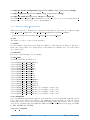
1 Introduction
The Ndigo5G is a digitizer and transient recorder designed to sample relatively shorts pulses
in rapid repetition. It produces a stream of output packets, each containing data from a single
trigger event together with a timestamp.
1.1 Features
10 bit dynamic range
up to 5 Gsps sample rate (in 1 channel mode)
up to 4 channels
digital input with TDC that can also be used for gating and triggering
2nd digital input for gating or triggering
PCIe 4x 1.0 with 800 MB/s throughput
multiple boards can be synchronized
extension board with 4 additional digital inputs.
1
2 Hardware
2.1 Installing the Board
The Ndigo5G board can be installed in any x4 (or higher amount of lanes) PCIe slot. If the slot
electrically supports less than 4 lanes, the board will operate at lowerdata throughput rates.
Please ensure proper cooling of the device. The Ndigo5G has an onboard temperature detection. If the ADC chip temperature exceeds 90◦ C a warning is issued to the device driver. In case
the temperature is higher than 95◦ C the ADC is disabled to avoid damage. Using a PCI-slot
cooler is in many cases an appropriate solution to circumvent problems caused by overheating
if the board is used inside a PC. The Ndigo-Crate will provide sufficient cooling under normal
operating conditions.
Using a single Ndigo5G, no further connections need to be made. For applications that
require more than 4 ADC channels, several Ndigo boards can be operated in sync. Any board
of the Ndigo product line can be synced to other Ndigo boards, allowing, for instance, for a
combination of high speed ADCs (Ndigo5G) and slower high resolution ADCs (Ndigo250M-14)
or the upcoming Ndigo TDC.
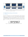
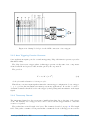
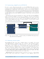
The signals used for board synchronization and inter-board triggering are transferred on a
bus be-tween the boards. Join all C2 connectors (see Figure 2.3 on page 5) on the boards using
a ribbon cable. Both ends of the bus need to be terminated properly. If using a Ndigo Crate,
connectors providing the termination are located on the crate mainboard next to the PCIe slots
to the extreme left and right. For more details, please refer to the Ndigo Crate user guide. In
applications that use only a few Ndigo boards installed directly inside a PC, termination PCBs
available from cronologic can be used.
Ndigo5G’s standard device driver can be used to read out all boards and acquire data. For
more complex scenarios, using the cronoSync-library, which is part of cronoTools, is recommended. The cronoSync library is provided with the Ndigo device driver. Please refer to the
cronoTools user guide for more information.
3
termination
C2
C2
C2
termination
C1
C1
C1
Figure 2.1: If several Ndigo boards are connected to work in sync , the boards must be connected
using a ribbon cable as bus for synchronization and trigger signals. At both ends of
the cable, proper termination is required.
2.2 Ndigo5G External Inputs and Connectors
2.2.1 Connectors
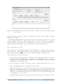
The inputs of the Ndigo5G are located on the PCI bracket. Figure 2.3 on page 5 shows the
location of the 4 analog inputs A to D and the two digital inputs G (GATE) and T (Trigger).
Furthermore, two board interconnection connectors can be found at the top edge of the Ndigo5G,
as displayed in Figure 2.3 on page 5. Connector C1 is used for a board-to-board connection (e. g.
to link a HPTDC8-PCI and a Ndigo5G via a Ndigo Extension board, see chapter 2.3). Connector
C2 is used as a bus interface between multiple Ndigo boards distributing clock, trigger and sync
signals. Proper termination must be placed at both ends of the bus interconnection ribbon
cable.
Figure 2.2: Input connectors of an Ndigo5G located on the PCI bracket.
cronologic GmbH & Co. KG
4
Ndigo5G User Guide
C2
C1
T
D
C
B
A
G
Figure 2.3: Schematics of an Ndigo5G board showing inter-board connectors C1 and C2.
2.2.2 Analog Inputs
LemoD00 connector
EV10AQ190
DAC
TC1-1-I3M+
analog-offset[i]
Figure 2.4: Input circuit for each of the four analog channels.
The analog inputs of the ADC are single ended LEMO00 coax connectors. The inputs have
a 50Ω impedance and are AC coupled. The inputs are converted to a differential signal using a
balun.
Analog Offsets
AC coupling removes the common mode voltage from the input signal. Users can move the
common mode voltage to a value of their choice using the analog offset parameter of each
channel before sampling.
This feature is useful for highly asymmetric signals, such as pulses from TOF spectrometers
or LIDAR systems. Without analog offset compensation, the pulses would begin in the middle
of the ADC range, effectively cutting the dynamic range in half. By shifting the DC baseline to
one end of the ADC range, the input range can be used fully, providing the maximum dynamic
range. The analog offset can be set between ±0, 25V
cronologic GmbH & Co. KG
5
Ndigo5G User Guide
+0,25V
+0,25V
0,1V
-0,25V
-0,25V
analog_offset[i] = 0V
analog_offset[i] = 0,1V
Figure 2.5: Users can add analog offset to the input before sampling
+0,25V
+0,25V
0,22V
-0,25V
-0,25V
analog_offset[i] = 0V
analog_offset[i] = -0,22V
Figure 2.6: Asymmetric signal shifted to increase dynamic range
2.2.3 Digital Inputs
There are two digital inputs on the front slot cover called Trigger and GATE.
Both inputs provide a digital input signal routed to the trigger matrix. These signals can be
used to trigger any of the trigger state machines and gating blocks. The inputs are AC coupled.
DC offset is configurable via the dc offset parameter in the configurations structure to support
positive and negative input pulses.
The configuration is set via the structures trigger[8] and trigger[9] in the configuration structure. The input circuit is shown in Figure 2.17 on page 13.
TDC on Trigger Input
There is a TDC connected to the Trigger input. When used with the TDC, the Trigger input
supports negative pulses only . The TDC creates packets of type 8. These packets first contain
a coarse timestamp and a payload that can be used to calculate the trigger position with higher
precision. The function ndigo process tdc packet() can be used to replace the coarse timestamp
with the precise timestamp. This function is described in section 3.5 on page 38. TDC pulses
must have a minimum duration of 3.3ns. The dead-time of the TDC is 32ns.
cronologic GmbH & Co. KG
6
Ndigo5G User Guide
2.3 Extension Card
The Ndigo Extension card provides additional inputs or outputs to the FPGA. It is connected
to the Samtec QSS-025 connector on an Ndigo5G by an Samtec SQCD cable assembly.
The Ndigo Extension Card provides up to ten single ended LEMO00 connectors. The circuit
connecting to each of these circuits can be chosen to provide inputs or outputs. These can be
AC or DC coupled. AC coupled inputs support NIM signaling.
The signals connect to 2.5V IO Pins of the Xilinx Virtex-5 FPGA. The current firmware
revision provides the following signal connections:
Connector
QSS Pin
FPGA Pin
Direction
Signal
LEMO00: CH0
22
AD9
Input
Ndigo Extension digital channel 0
LEMO00: CH1
18
AE10
Input
Ndigo Extension digital channel 1
LEMO00: CH2
14
D10
-
not connected
LEMO00: CH3
10
AF9
Output
39 MHz clock for HPTDC
LEMO00: CH4
6
AD11
Output
39 MHz clock for HPTDC
LEMO00: CH5
5
AE7
Output
39 MHz clock for HPTDC
LEMO00: CH6
9
AF7
Output
39 MHz clock for HPTDC
LEMO00: CH7
13
D9
-
not connected
LEMO00: CH8
17
V9
Input
Ndigo Extension digital channel 2
LEMO00: CH9
21
W9
Input
Ndigo Extension digital channel 3
SYNC1: Sync-TDC8
26
F9
-
not connected
SYNC1: Sync-HPTDC
44
AA7
Output
Sync for HPTDC
The 4 digital inputs are routed to the bus inputs of the trigger matrix to be used for triggering.
The routing can be configured to either ORing the sync bus and extension channels or use the
extension channels exclusively.
Connector
Extension Card
Trigger matrix input
Trigger matrix input
Digital Channel
ignore cable = 0
ignore cable = 1
LEMO00: CH0
0
BUS0 = EXT0 | Sync Cable 0
BUS0 = EXT0
LEMO00: CH1
1
BUS1 = EXT1 | Sync Cable 1
BUS1 = EXT1
LEMO00: CH8
2
BUS2 = EXT2 | Sync Cable 2
BUS2 = EXT2
LEMO00: CH9
3
BUS3 = EXT3 | Sync Cable 3
BUS3 = EXT3
2.4 Ndigo5G Functionality
cronologic GmbH & Co. KG
7
Ndigo5G User Guide
2.4.1 ADC Modes
Depending on board configuration, the analog input signal is quantized to 8 or 10 bits. However,
the board always scales and offsets the data to 16 bit signed data centered around 0.
Data processing such as trigger detection or packet building are always performed on 3.2ns
intervals. Depending on the ADC mode, this interval may contain 4, 8 or 16 samples.
The board supports using one, two or four channels:
1 Channel Modes A, B, C and D
In these modes, only a single channel is used. The analog signal on that channel is digitized at
5Gsps. Packet size is always a multiple of 16 samples per 3.2ns. See Figure 2.9 on page 9 and
Figure 2.15 on page 13.
2 Channel Modes AC, BC, AD and BD
In these modes, two channels are used simultaneously. The analog signals on these channels are
digitized at 2.5Gsps each. Packet size is always a multiple of 8 samples per 3.2ns. See Figure
2.8 on page 9 and Figure 2.14 on page 12.
4 Channel Mode ABCD
In this mode, all four channels are digitized independently at 1.25Gsps each. The packet size is
always a multiple of 4 samples per 3.2ns. See Figure 2.7 on page 9 and Figure 2.13 on page 12.
Multiple Sampling Modes AAAA, BBBB, CCCC and DDDD
In these modes, only one analog input channel is used, but the channel is sampled independently
and simultaneously by four ADCs at 1.25Gsps. The board creates four independent streams with
4 samples each per 3.2ns.
Using the same trigger setting on all ADCs, can be used to reduce noise by averaging the four
channels. To deal with complex triggering conditions, different trigger settings on each of the
ADCs can be used.
The Ndigo5G provides 4 ADCs sampling at 1.25Gsps each. Higher speed modes are implemented by interleaving two or four of these ADCs.
During interleaving, the Ndigo5G firmware reorders and groups the data into a linear sample
stream. The process is fully transparent. For users, the only difference is that a 3.2ns cycle can
contain 4, 8 or 16 samples, depending on mode.
cronologic GmbH & Co. KG
8
Ndigo5G User Guide
1.25 GHz
CLK
(2.5 GHz)
Clock
circuit
ADC A
1.25 Gsps
ADC B
1.25 Gsps
ADC C
1.25 Gsps
ADC D
1.25 Gsps
AAI, AAIN
BAI, BAIN
CAI, CAIN
DAI , DAIN
Figure 2.7: ADCs in 4 channel mode ABCD at 1.25Gsps.
Inverted
1.25 GHz
CLK
(2.5 GHz)
Clock,
circuit
ADC,A
1.25 Gsps
ADC,B
1.25 Gsps
ADC,C
1.25 Gsps
ADC,D
1.25 Gsps
In-phase
1.25 GHz
AAI,,AAIN
DAI,,DAIN
Figure 2.8: ADCs in 2 channel mode AD, interleaved for 2.5Gsps.
90 0 phase-shifted 2700 phase -shifted
1.25 GHz
1.25 GHz
CLK
72.5 GHz)
Clock,
circuit
ADC,A
1.25 Gsps
In-phase
1.25 GHz
ADC,B
1.25 Gsps
ADC,C
1.25 Gsps
ADC,D
1.25 Gsps
Inverted
1.25 GHz
AAI,,AAIN,or,BAI,BAIN,or,CAI ,,CAIN,or,DAI ,,DAIN
Figure 2.9: ADCs in 1 channel mode A, B, C or D interleaved for 5Gsps.
cronologic GmbH & Co. KG
9
Ndigo5G User Guide
2.4.2 Zero Suppression
One of Ndigo 5G’s key features is on-board zero suppression to reduce PCIe bus load. Only data
that passes specifications predefined by the user is transmitted. This guide refers to transmitted
wave form data as “packets”. A packet contains the wave form data and a timestamp giving
the absolute time (i.e. the time since start of data acquisition) of the packet’s last sample.
Figure 2.10 shows a simple example: Data is written to the PC only if values exceed a specified
threshold. Expanding on that, Ndigo 5G’s zero suppression can be used to realize much more
complex scenarios.
Retrigger
Postcursor
timestamp
timestamp
Precursor
Figure 2.10: Simple zero suppression: Only data with values above a threshold are written to
the PC.
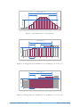
2.4.3 Trigger Blocks
Ndigo5G-10 and Ndigo5G-8 record analog wave forms using zero suppression. Whenever a
relevant waveform is detected, data is written to an internal FIFO memory. Each ADC channel
has one trigger block determining whether data is written to the FIFO. The parameters are set
in Structure ndigo trigger block(See chapter 3.4.3 on page 34).
Each trigger block consists of two independent units that check the incoming raw data stream
for trigger conditions (Fig. 2.10 on page 10). Users can specify a threshold and can choose
whether triggering is used whenever incoming data is below or above the threshold (level triggering) or only if data exceeds the threshold (edge triggering).
A gate length can be set to extend the trigger window by multiples of 3.2ns. Furthermore, if
users choose precursor values > 0, the trigger unit will start writing data to the FIFO precursor ·
3.2ns before the trigger event.
When using edge triggering, all packets have the same length (Figure 2.11 on page 11):
cronologic GmbH & Co. KG
10
Ndigo5G User Guide
precursor + length + 1 cycles of 3.2ns. For level triggering, packet length is data dependent
(Figure 2.12 on page 12).
Please note that triggering is not accurate to sample. For each 3.2ns clock cycle, it is determined whether on any sample during that clock cycle a trigger condition is met. The clock cycle
is then selected as the trigger point. As a result, the trigger sample can be anywhere within a
range of up to 16 samples in single channel mode (Figure 2.15 on page 13) at 16 samples per
3.2ns.
If retriggering is active, the current trigger window is extended if a trigger event is detected
inside the window.
A trigger block can use several input sources:
the 8 trigger decision units of all four ADC channels (Figure 2.16 on page 13)
the GATE input (Figure 2.17 on page 13)
the Trigger input (Figure 2.17 on page 13)
a function trigger providing random or periodic triggering (Section 2.4.5 on page 18)
triggers originating from other cards connected with the sync cable or from the Ndigo
Extension card (BUS0, BUS1, BUS2, BUS3)
A second set of trigger units for the digital inputs Trigger, GATE, BUS0, BUS1, BUS2,
and BUS3 that is set in hardware to positive edge triggering. This set of triggers is not
available as inputs for the gate blocks.
Trigger inputs from the above sources can be concatenated using logical “OR” (Figure 2.19
on page 14) by setting the appropriate bits in the trigger blocks source mask.
Triggers can be fed into the gate blocks described on page 15 (Figure 2.20). Gate blocks can
be used to block writing data to the FIFO. That way, only zero suppressed data occurring when
the selected gate is active is transmitted. This procedure reduces PCIe bus load even further
(Figure 2.20).
total length = 19
length = 12
threshold
precursor = 6
Figure 2.11: Parameters for edge triggering
cronologic GmbH & Co. KG
11
Ndigo5G User Guide
total length = 21
length = 6
threshold
precursor = 6
Figure 2.12: Parameters for level triggering
total length = 4
precursor = 1
threshold
length = 2
3200 ps
Figure 2.13: Triggering in 4 channel mode at 4 samples per clock cycle.
total length = 4
precursor = 1
threshold
length = 2
3200 ps
Figure 2.14: Triggering in 2 channel mode at 8 samples per clock cycle.
cronologic GmbH & Co. KG
12
Ndigo5G User Guide
total length = 4
precursor = 1
threshold
length = 2
3200 ps
Figure 2.15: Triggering in 1 channel mode at 16 samples per clock cycle.
trigger 1
Z-1
sample data
threshold
rising
edge
trigger 2
Z-1
threshold
rising
edge
Figure 2.16: From the ADC inputs, a trigger unit creates an input flag for the trigger matrix.
Each digitizer channel (A, B, C, D) has two trigger units.
Z-1
input
rising
edge
Figure 2.17: The digital inputs Trigger, GATE, BUS0, BUS1, BUS2 and BUS3 have simpler
trigger units.
cronologic GmbH & Co. KG
13
Ndigo5G User Guide
enable
extension input
ignore_cable
cable sync
Figure 2.18: The extension block combines signals from the optional extension board and the
sync cable.
ext1 extension
sync1 block
ext2 extension
sync2 block
ext3 extension
sync3 block
digital
trigger
digital
trigger
digital
trigger
digital
trigger
bus0_pe
bus0
bus1_pe
bus1
bus2_pe
bus2
bus3_pe
bus3
1f
func_trigf
ext0 extension
sync0 block
digital
trigger
gate_pe
gate
GATE
D1
digital
trigger
tdc_pe
tdc
Trigger
C1
analog
trigger
C0
D0
Df
analog
trigger
B0
B1
Cf
analog
trigger
A1
Bf
analog
trigger
A0
Af
Gatesf
trigger_f
block[0]f
trigger_f
block[1]f
trigger_f
block[2]f
trigger_f
block[3]f
timefstampf
channelf
bus[0]f
bus[2]f
bus[3]f
tofcablefsyncf
bus[1]f
Figure 2.19: Trigger Matrix: The trigger signals of each ADC channel, the Triggerinput, the
GATE input or the sync cable can be combined to create a trigger input for each
trigger block. The four gate signals can be used to suppress triggers during certain
time frames.
cronologic GmbH & Co. KG
14
Ndigo5G User Guide
2.4.4 Gating Blocks
Trigger
Figure 2.20: Gating Blocks: Each gating block can use an arbitrary combination of inputs to
trigger its state machine. The outputs can be individually inverted and routed to
the AND-gate feeding the trigger blocks.
To decrease the amount of data transmitted to the PC, Ndigo5G includes 4 independent gate
and delay units. A gate and delay unit creates a gate window starting at a specified time after
a trigger, closing the window at gate stop. Both timing values gate start and gate stop must
be set as multiples of 3.2ns.
Trigger blocks can use the gate signal to suppress data acquisition: Only data that fulfills
zero suppression specifications occurring in an active gate window is written to the PC.
As input, any trigger from the 4 trigger blocks, the GATE and Trigger inputs, a trigger from
a connected board and the function generator can be used.
The retrigger feature will create a new gate if a trigger occurs during an active gate window.
The gate signal can be inverted, causing an active gate to close for a time defined by the user.
The parameters of a gating block are set in Structure ndigo gating block described on page
36.
Figure 2.21 shows the functionality of the gate timing and delay unit. Active gate time is
marked in green.
cronologic GmbH & Co. KG
15
Ndigo5G User Guide
Trigger
Gate
Gate Start
Gate Stop
Figure 2.21: Gate and delay functionality: When a trigger occurs, the gate opens after a set
period of time (“gate start”) and closes when it reaches “gate stop”.
Gating Example 1: Suppression of Noise After Starting an Acquisition
In mass spectrometer and other experiments, noise while starting data acquisition can result
in undesired trigger events for that time period. To prevent noise in the output data, a gating
block could be used to suppress all triggers during start-up.
The following example illustrates the use of a gating block to prevent noise: The GATEinput
transmits a pulse on each acquisition start. The trigger structure of the GATE input is used to
select pulse polarity. Then, the GATE trigger is selected as gating block input and the gating
block’s start parameter is set to 0. The stop parameter is set to the desired length measured in
3.2ns clock cycle and negate is set to true. The gating block will now output a low pulse of the
desired length whenever there is a pulse on the GATE input.
Enabling this gating block as an AND input to the trigger block, for which noise shall be
suppressed.
Gating Example 2: Delayed Trigger
To sample a short window at a specified time after a trigger event on a channel, the gating
block can be used to create a delayed trigger. To do this, one of the triggers of the channel of
interested is configured to the desired parameters by selecting the threshold, setting the edge
polarity and enabling edge triggering.
Instead of directly using this trigger as input to the trigger block’s input matrix, the trigger is
selected as an input to a gating block. The block is configured to start = delay [in 3.2ns clock
cycles] and stop = start + 1, negate = f alse. This causes the gating block to produce a one
clock cycle pulse on its output after the specified delay.
To send this pulse to the trigger block, the gating block must be enabled in the trigger block’s
AND matrix and the ONE trigger source must be selected.
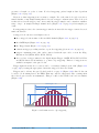
Gating Example 3: Dual Level Trigger
The gates provide AND connections between each other (see fig. 2.19) which can be used for
example in a dual level trigger. For the acquisition of signal data with amplitudes between a
lower and an upper bound, for example, two level triggers can be connected (see fig. 2.22): a
falling level trigger with an upper threshold and a rising level trigger with a lower threshold.
cronologic GmbH & Co. KG
16
Ndigo5G User Guide
Since the triggers are only connected by OR in the triggerblock logic (see fig. 2.19) they are
assigned to one of the gates each and connected with AND via the gating block region of the
trigger matrix (see fig. 2.19 and 2.23). Because of the dead times of the gates it is important
to enable the retriggering feature. Furthermore a precursor of 2 clock cycles is needed, because
the gates are delayed in relation to the ADC samples.
upper threshold
lower threshold
upper level trigger
lower level trigger
upper AND lower
Figure 2.22: Measuring data with amplitude between an upper and a lower threshold by means
of two level triggers.
Config settings can be found in the following code snippet.
1
2
3
4
5
6
7
8
9
10
11
12
13
config . t r i g g e r b l o c k [ 0 ] . enabled = 1;
config . trigger block [ 0 ] . precursor = 2;
config . trigger block [ 0 ] . length = 0;
c o n f i g . t r i g g e r b l o c k [ 0 ] . s o u r c e s = NDIGO TRIGGER SOURCE ONE ;
c o n f i g . t r i g g e r b l o c k [ 0 ] . g a t e s = NDIGO TRIGGER GATE 0 | ←NDIGO TRIGGER GATE 1 ;
config . gating block [ 0 ] . r e t r i g g e r = 1;
config . gating block [ 0 ] . stop = 0;
config . gating block [ 1 ] . r e t r i g g e r = 1;
config . gating block [ 1 ] . stop = 0;
c o n f i g . g a t i n g b l o c k [ 1 ] . s o u r c e s = NDIGO TRIGGER A1 ;
c o n f i g . t r i g g e r [ NDIGO TRIGGER A0 ] . t h r e s h o l d = 1 0 0 0 0 ;
c o n f i g . t r i g g e r [ NDIGO TRIGGER A1 ] . r i s i n g = 1 ;
c o n f i g . t r i g g e r [ NDIGO TRIGGER A1 ] . t h r e s h o l d = −10000;
cronologic GmbH & Co. KG
17
Ndigo5G User Guide
Trigger
Figure 2.23: Gating block logic for the AND connection of two triggers.
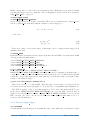
2.4.5 Auto Triggering Function Generator
Some applications require periodic or random triggering. Ndigo5G’s function generator provides
this functionality.
The delay between two trigger pulses of this trigger generator is the sum of two components:
A fixed value M and a pseudo random value given by the exponent N.
The period is
T = 1 + M + [1...2N ]
(2.1)
clock cycles with a duration of 3.2 ns per cycle.
This allows to monitor input signals at times the current trigger configuration does not trigger,
e. g. to get base line information in mass spectrometry applications. It can also be used to
determine a suitable threshold level for the trigger by first getting random statistics on the input
signal.
2.4.6 Timestamp Channel
The timestamp channel produces a stream of small packets that denote the time of the trigger
event. An arbitrary set of trigger sources can be selected in the trigger matrix to cause the
creation of a packet.
The packets have a fixed length of 16 bytes. The format is described on page 41. The length
field of the packet contains a 32 bit pattern that contains the levels of all trigger sources at the
cronologic GmbH & Co. KG
18
Ndigo5G User Guide
time of the trigger event except for the period monitor. Only one packet is created, no matter
how many trigger sources caused the timestamp channel to trigger.
2.4.7 Data Lookup Table
In some applications it might be useful to modify the ADC sample data by a user defined function
f (x). In this case the onboard FPGA is able to perform this task such that the the data stream
consists of data words f (sample) instead of sample. The function f(x) is applied using a 1024
word lookup table (LUT) which needs to be provided by the user. This is done by defining
the corresponding function as a custom lut-member of the ndigo configuration structure. Please
feel free to contact cronologic if you plan the use this feature. The onboard INL correction is
applied prior to mapping the LUT values.
2.5 Multiple Ndigo boards synchronization
Using several Ndigo devices in applications that use more channels than a single board can
provide requires synchronized operation. To ensure exact synchronization, a delay parameter
needs to be set for each board. This parameter might change in case boards are swapped, added
or removed and in some cases might change after a firmware update.
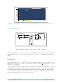
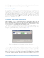
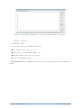
The calibration tool “MultiboardCalibration.exe” is available after installing the Ndigo device
driver. It is used to find appropriate delay values for each board in a given board setup. After
starting, the application lists all Ndigo boards found (Figure 2.24).
Figure 2.24: Main window of the multiple boards sync calibration tool.
A board’s appropriate delay depends on whether it operates in master or slave mode. The
respective values can be set in the column “Delay M” (for master boards) and “Delay S” (for
slave boards). The designated master board can be selected in the column “Master”. The
calibration procedure creates a histogram for each board, displaying the current delay between
the boards. The histogram can be viewed by clicking on “Show!”. When the appropriate delay
values are found, they can be stored in the on-board flash prom by clicking “Do it!” separately
for each board. Clicking “Flash All!” will write the values to all boards at once. Please note:
cronologic GmbH & Co. KG
19
Ndigo5G User Guide
Flashing the values might take up to 10 seconds during which the program might not respond.
Important note:If the application reports a “PLL not locked” error check the cable. If the
recording of histograms does not make progress check the cable. Make sure the cable is properly
terminated at both ends and firmly attached to each card.
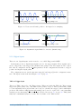
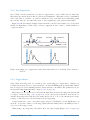
2.5.1 Calibration Procedure
1. Make sure the “Automode” is selected.
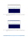
2. Record the calibration histograms by pressing “Record histograms”. The program will
perform up to 200 measurements of the sync delay. After accumulating some data, the
delay values found are reported in the column “AutoMmt”. The values can be verified
by examining histogram that was recorded. A board’s histogram should look like the one
shown in Figure 2.25. During normal operation the delay will be adjusted such, that the
data points accumulated roughly coincide with the vertical markers in the upper panel.
As the delay pattern is periodic, valid delay values are between 0 and 31. Thus, the
delay value found by the auto measurement should correspond to the distance between
the vertical markers and accumulated data points. Hint: when moving the mouse pointer
across the histogram the delay value of the current location is displayed.
3. After stopping the data acquisition (by pressing “Record Histograms” again) the delay
values of the auto measurement need to be copied to the columns “Delay M” or “Delay
S” depending on the corresponding board being a master or a slave. The correct field to
copy the value to is highlighted in green.
4. you may record recorded a new dataset as a crosscheck that the delay is now set to an
appropriate value. By disabling “Automode” the new delay values are used. Press “Record
Histograms” in order to start the data acquisition. After some time the histogram should
look similar to the one in Figure 2.26.
5. The delay values for all boards in a set needs to be found. For the case a board acts as
a master, the value “Delay M” needs to be adjusted, in case it is a slave, the “Delay S”
parameter needs to be changed. In order to find the master-case delay values for all boards,
the calibration procedure needs to be performed with every board acting as a master once.
After changing the master board, the slave values of the other boards don’t need to be
readjusted. Only Ndigo5G boards may be set as masters. Therefore, a Ndigo250M board
only needs to be calibrated as a slave.
6. After finding all delay values, write the values to the on-board flash PROMs by pressing
“Flash All!”.
cronologic GmbH & Co. KG
20
Ndigo5G User Guide
Figure 2.25: Histogram for the case the delay value for the board is not set correctly. Please
note: the lower panel might differ from board to board, with the “step” being at a
different position.
Figure 2.26: Histogram for the case the delay value for the board is set correctly. Please note: the
lower panel might differ from board to board, with the “step” being at a different
position.
cronologic GmbH & Co. KG
21
Ndigo5G User Guide
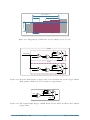
2.5.2 Synchronizing a Ndgio5G and an HPTDC8-PCI
In order to operate a Ndigo5G in sync with one ore more HPTDC8-PCI boards, a board to
board in -terconnection using a Ndigo Extension Board needs to be done. The Ndigo Extension
Board has four clock outputs. One of them needs to be connected to the external clock input of
the HPTDC using a standard Lemo 00 cable. The Ndigo5G is connected to the Ndigo Extension
Board using the Samtec ribbon cable provided with the Ndigo Extension Board. The signals used
for synchronization of the boards are transmitted by a standard 10pin ribbon cable connecting
the Ndigo Extension Board and the HPTDC. A schematic of all necessary connections is shown
in Figure 2.27.
In principle the user can use the standard device drivers of the Ndigo5G and the HPTDC8PCI to perform data acquisition. It is, however, recommended to use the cronoSync-library,
which is a part of the cronoTools provided with with the Ndigo5G device driver. CronoSync
offers an easy group-based access to the data recorded and handles the synchronization of all
cronologic data ac-quisition devices used. A detailed description of cronoTools and cronoSync
can be found in the cronoTools user guide.
C1
C2
Figure 2.27: Interconnection scheme of a Ndigo5G (left) and a HPTDC8-PCI (right) using a
Ndigo Extension Board (middle).
2.5.3 Performing a firmware update
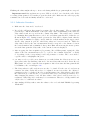
After installing the Ndigo device driver, a firmware update tool is available. By choosing
“NdigoFirmwareGUI.exe” a firmware update can be performed. After invoking the application a window as shown in Figure 2.28 will appear. The tool can be used for updating the
firmware and to create a backup of the on-board calibration data of the Ndigo unit. If several
boards are present, the one which is going to be used can be selected in the upper left corner of
the window. Pressing the “Backup” buttons a backup of the firmware or the calibration data
will be created, respectively. In order to perform a firmware update, chose the “.ndigorom”-file
to used by pressing “Browse”. The file contains the firmware proms for all boards of the Ndigo
product line. By pressing “Flash” the firmware is written to the board. “Verify” can be used
to compare the data stored inside the prom to the one inside a file.
Important note: The new firmware will only be used after a power cycle, i.e. after switching
the PC (or Ndigo crate) off and back on. A simple reboot is not sufficient. Therefore the
cronologic GmbH & Co. KG
22
Ndigo5G User Guide
Figure 2.28: The firmware update and calibration data backup tool as provided with the Ndigo
device driver.
information shown in the upper half of the application window does not change right after
flashing a new firmware.
After flashing and shutting the PC or the crate off and on again it is recommended to perform
a window calibration. The tool “WindowCalibration” is provided for that purpose within the
driver installation. The Omission of the calibration process leads to longer execution times of
applications using that firmware, since the calibration is performed then instead.
2.5.4 Calibrating the TDC
After each update of the Ndigo5G-10 firmware the TDC has to be calibrated. The calibration
is done with the tool “TDC Calibration.exe” which is available after installing the Ndigo device
driver. After invoking the application a window as shown in Figure 2.29 will appear.
The calibration procedure is as follows:
1. Connect an external pulse signal to the Trigger input. The signal should be low active
with a frequency in the kHz range. It must not be synchronized to the clock source of
the Ndigo5G-10. The input frequency must not exceed 10 MHz. The pulse low and high
width has to be at least 10ns each.
2. Set Serial Number according to the sticker on the card if the shown value is not correct.
3. Start capturing pulse events by pressing the Start button.
4. Adjust the Input Offset so that First Bin is in the range of 4 to 16. If First Bin is less
than 4, increment Input Offset by one. If First Bin is greater than 16 decrement Input
Offset by one. Repeat increment/decrement until First Bin is in the range of 4 to 16.
Depending on the firmware revision the Input Offset value for a successful calibration may
be in the range of 6 10 or 28 32.
5. When the Write Calibration Data button becomes enabled press it to update the calibra-
cronologic GmbH & Co. KG
23
Ndigo5G User Guide
Figure 2.29: The TDC calibration tool as provided with the Ndigo device driver.
tion data on the card.
6. Calibration done!
The card can only be successfully calibrated if:
First Bin is in the range of 4 to 16
Empty Bins is less than (First Bin + 4)
at least 10,000 events have been captured
a valid serial number is set.
Important note: If the application reports an error check if the input pulse is within specification.
cronologic GmbH & Co. KG
24
Ndigo5G User Guide
3 Driver Programming API
The API is a DLL with C linkage. There exists also a .Net wrapper.
The functions provided by the DLL are declared in Ndigo interface.h.
3.1 Constants
#define NDIGO CHANNEL COUNT 4
The number of analog input channels.
#define NDIGO GATE COUNT 4
The number of gating blocks.
#define NDIGO TRIGGER COUNT 16
The number of triggers. Two per analog input, one per digital input plus some specials.
#define NDIGO ADD TRIGGER COUNT 6
Additional set of triggers for digital inputs.
3.2 Initialization
int ndigo count devices(int *error code, char **error message)
Return the number of boards that are supported by this driver in the system.
int ndigo get default init parameters(ndigo init parameters *init)
Get a set of default parameters to feed into ndigo init(). This must always be used to initialize
the ndigo init parameter structure.
ndigo device *ndigo init(ndigo init parameters *params, int *error code, char **error message)
Open and initialize the Ndigo board with the given index. With error code and error message
the user must provide pointers where to buffers where error information should be written by
the driver. The buffer for the error message must by at least 80 chars long.
Params is a structure of type ndigo init parameters that must be completely initialized.
int ndigo close(ndigo device *device)
Finalize the driver for this device.
3.2.1 Structure ndigo init parameters
int version
Must be set to NDIGO API VERSION
25
int card index
The index in the list of Ndigo5G boards that should be initialized. There might be multiple
boards in the system that are handled by this driver as reported by ndigo count devices. This
index selects one of them. Boards are enumerated depending on the PCIe slot. The lower the
bus number and the lower the slot number the lower the card index.
int board id
This 8 bit number is filled into each packet created by the board and is useful if data streams of
multiple boards will be merged. If only Ndigo5G cards are used this number can be set to the
card index. If boards of different types that use a compatible data format are used in a system
each board should get a unique id. Can be changed with int ndigo set board id(ndigo device
*device, int board id).
ndigo bool t use external clock
Use 10MHz clock supplied by IPC flat band cable. Must be set for all slaves.
ndigo bool t drive external clock
Drive internal 10MHz clock of this board to IPC flat band cable. Must be set for master.
ndigo bool t is slave
Data acquisition of this board is controlled by the master board.
int sync period
Period of the multicard sync pulse. Should be set to 4 (default) when using several Ndigo boards
in sync. Ignored for single board setups. The Ndigo5G has 4 phases relative to the global 10MHz
clock.
int sync delay
Fine tap delay for incoming sync signals.
ndigo bool t force window calibration
If true/1, valid data window is detected at initialization. Default value is false/0: values from
flash memory are used in order to set data window to correct position.
ndigo bool t hptdc sync enabled
A HPTDC is connected to this board. Enables the clock and sync line from the Ndigo5G to the
HPTDC.
int64 buffer size[8]
The minimum size of the DMA buffer. If set to 0 the default size of 16MByte is used. Ndigo5G
only uses buffer size[0].
int buffer type
Must be set to D125 BUFFER ALLOCATE.
int64 buffer address
Ignored. Might be used for future buffer types.
int variant
Set to 0. Can be used to activate future device variants such as different base frequencies.
int device type
Initialized by ndigo get default init parameters(). Must be left unchanged.
#define CRONO DEVICE HPTDC 0
#define CRONO DEVICE NDIGO5G 1
cronologic GmbH & Co. KG
26
Ndigo5G User Guide
#define CRONO DEVICE NDIGO250M 2
3.3 Status Information
3.3.1 Functions for Information Retrieval
The driver provides functions to retrieve detailed information on the type of board, its configuration, settings and state. The information is split according to its scope and the computational
requirements to query the information from the board.
int ndigo get static info(ndigo device *device,ndigo static info *info)
This structure contains information about the board that does not change during run time.
int ndigo get param info(ndigo device *device, ndigo param info *info)
The structure returned by this call contains information that changes indirectly due to configuration changes.
int ndigo get fast info(ndigo device *device, ndigo fast info *info)
This call returns a structure that contains dynamic information that can be obtained within a
few microseconds.
int ndigo get slow info(ndigo device *device, ndigo slow info *info)
The data reported in this structure requires milliseconds to be obtained. The application should
only call it in situation where the program flow can cope with an interruption of that magnitude.
3.3.2 Structure ndigo static info
This structure contains information about the board that does not change during run time. It
is provided by the function ndigo get static info.
int size
The number of bytes occupied by the structure
int version
A version number that is increased when the definition of the structure is changed. The increment can be larger than one to match driver version numbers or similar. Set to 0 for all versions
up to first release.
int board id
Index of the board as passed to the constructor or set via int ndigo set board id(ndigo device
*device, int board id).
int driver revision
The lower three bytes contain a triple level hierarchy of version numbers, e.g. 0x010103 encodes
version 1.1.3.
A change in the first digit generally requires a recompilation of user applications. Change in
the second digit denote significant improvements or changes that don’t break compatibility and
the third digit changes with minor bugfixes and similar updates.
int firmware revision
Firmware revision of the FPGA configuration. This increments only when there is a functional
change.
cronologic GmbH & Co. KG
27
Ndigo5G User Guide
int board revision
0 for experimental prototypes labeled “Rev. 1”
2 for the version produced until 2010 labeled “Rev. 2”‘
3 for the version produced starting in 2011 labeled “Rev. 3”
int board configuration
Describes the schematic configuration of the board.
For board revision 0 this always reads 0.
For board revision 2 the following assignments are valid:
If Bit 3 = 0 this following is valid:
Bit 0 determines the ADC resolution. (0 = 8 − bit or 1 = 10 − bit ).
Bit 1 determines whether the TDC-oscillator is present (0 = oscillator present, 1 = simple trigger).
Bit 2 determines the input connectors (0 = single ended, 1 = differential).
Bit 3 = 1 signifies a special version of the board
0xA is Ndigo1250M-12 single ended with digital trigger
0x8 is Ndigo5G-8 single ended with digital trigger
For Board revision 3 the following assignments are valid:
Bit 2 determines the input connectors (0 = single ended, 1 = differential).
The other bits have one of the following patterns [Bits 3...0]
0010
0011
0110
1000
1010
1011
1110
1111
Ndigo5G-10 2.5u 10
Ndigo5G-8-AQ 2.5u 8
Ndigo5G-10-Diff 560pF 10 DIFF
Ndigo5G-8 560pF 8+
Ndigo1250M-12 2.2uF 12 Sciex DC
Ndigo5G-10 560pF 10
Ndigo5G-Sciex 2.2uF 10 Sciex Infiniband, DIFF
Ndigo5G-Roent = fADC4/10 560pF 10
int adc resolution
Number of bits of the ADC, set to 0 if unknown.
double nominal sample rate
Sample rate in once channel mode. Usually 5.0e9 = 5Gsps.
double analog bandwidth
3e9 for 3Ghz
int chip id
16 bit factory ID of the ADC chip
int board serial
Serial number with the year minus 2000 in the highest 8 bits of the integer and a running number
in the lower 24 bits. This number is identical with the one on the label on the board.
int flash serial low
int flash serial high
64 bit manufacturer serial number of the flash chip.
int flash valid
cronologic GmbH & Co. KG
28
Ndigo5G User Guide
If not 0 the driver found valid calibration data in the flash on the board and is using it.
ndigo bool t dc coupled
Returns false for the standard AC coupled Ndigo5G.
int subversion revision
A number to track builds of the firmware in more detail than the firmware revision. It changes
with every change in the firmware, even if there is no visible effect for the user.
char calibration date[20]
DIN EN ISO 8601 string YYYY-MM-DD HH:DD describing the time when the card was calibrated.
3.3.3 Structure ndigo param info
int size
The number of bytes occupied by the structure.
int version
A version number that is increased when the definition of the structure is changed. The increment can be larger than one to match driver version numbers or similar. Set to 0 for all versions
up to first release.
double bandwidth
Analog Bandwidth setting of the ADC. Either 3e9 = 3GHz or 1e9 = 1GHz for 10 bit version.
double sample rate
Sample rate. This is 1.25e9, 2.5e9 or 5.0e9 depending on the current ADC mode. sample rate ·
channels = 5.0e9.
double sample period
The period one sample in the data represents in picoseconds
int board id
The number the board uses to identify the data source in the output data stream.
int channels
Number of channels. 1, 2 or 4 depending on the ADC mode chosen. sample rate · channels =
5.0e9.
int channel mask
Mask with a set bit for each enabled input channel.
int64 total buffer
The total amount of the DMA buffer in bytes.
3.3.4 Structure ndigo fast info
int size
The number of bytes occupied by the structure
int version
A version number that is increased when the definition of the structure is changed. The increment can be larger than one to match driver version numbers or similar. Set to 0 for all versions
up to first release.
cronologic GmbH & Co. KG
29
Ndigo5G User Guide
int adc rpm
Speed of the ADC fan. Reports 0 if no fan is present.
int fpga rpm
Speed of the FPGA fan. Reports 0 if no fan is present.
int alerts
Alert bits from the system monitor.
Bit
Bit
Bit
Bit
Bit
Bit
0
1
2
3
4
5
:
:
:
:
:
:
FPGA temperature alert (> 85◦ C)
Internal FPGA voltage out of range (< 1.01V or > 1.08V )
FPGA auxiliary voltage out of range. (< 2.375V or > 2.625V )
FPGA temperature critical (> 125◦ C)
ADC temperature alert (> 90◦ C)
ADC temperature critical (> 100◦ C): will automatically be turned off.
double voltage aux
Auxiliary FPGA voltage, nominal 2.5V
double voltage int
Internal FPGA voltage, nominal 1.0V
double fpga temperature
In ◦ C measured on die.
int pcie link width
Number of PCIe lanes that the card uses. Should be 4 for Ndigo5G.
int pcie max payload
Maximum size in bytes for one PCIe transaction, depends on system configuration.
3.3.5 Structure ndigo slow info
int size
The number of bytes occupied by the structure.
int version
A version number that is increased when the definition of the structure is changed. The increment can be larger than one to match driver version numbers or similar. Set to 0 for all versions
up to first release.
double adc temperature
ADC temperature in ◦ C measured on die.
double board temperature
In ◦ C.
3.4 Configuration
The device is configured with a configuration structure. The user should first obtain a structure
that contains the default settings of the device read from an on board ROM , than modify the
structure as needed for the user application and use the result to configure the device.
int ndigo get default configuration(ndigo device *device, ndigo configuration *config)
cronologic GmbH & Co. KG
30
Ndigo5G User Guide
int ndigo get current configuration(ndigo device *device, ndigo configuration *config)
int ndigo configure(ndigo device *device, ndigo configuration *config)
int ndigo set board id(ndigo device *device, int board id)
The board id can be changed after initialization of the card. If cronotools are used the board id
changes have to be done before cronotools initialization.
3.4.1 Structure ndigo configuration
This is the structure containing the configuration information. It is used in conjunction with
ndigo get default configuration, ndigo get current configuration and ndigo configure.
It uses internally the structures ndigo trigger block and ndigo trigger.
int size
The number of bytes occupied by the structure.
int version
A version number that is increased when the definition of the structure is changed. The increment can be larger than one to match driver version numbers or similar. Set to 0 for all versions
up to first release.
int reserved1
Reserved for internal usage. Do not change.
int adc mode
Constant describing the ADC mode
#define
#define
#define
#define
#define
#define
#define
#define
#define
#define
#define
#define
#define
#define
#define
#define
#define
NDIGO
NDIGO
NDIGO
NDIGO
NDIGO
NDIGO
NDIGO
NDIGO
NDIGO
NDIGO
NDIGO
NDIGO
NDIGO
NDIGO
NDIGO
NDIGO
NDIGO
ADC
ADC
ADC
ADC
ADC
ADC
ADC
ADC
ADC
ADC
ADC
ADC
ADC
ADC
ADC
ADC
ADC
MODE
MODE
MODE
MODE
MODE
MODE
MODE
MODE
MODE
MODE
MODE
MODE
MODE
MODE
MODE
MODE
MODE
ABCD 0
AC 4
BC 5
AD 6
BD 7
A8
B9
C 10
D 11
AAAA 12
BBBB 13
CCCC 14
DDDD 15
A12 28 // not available on all boards
B12 29 // not available on all boards
C12 30 // not available on all boards
D12 31 // not available on all boards
double bandwidth
Set to the minimum bandwidth required for the application. Lower bandwidth results in reduced
noise. The driver will set the ADC to the minimum setting that has at least the desired
bandwidth and report the selected bandwidth in the ndigo param info structure. The -8, -10 and
-12 versions currently supports 1GHz and 3GHz bandwidth, the -8AQ version supports 2GHz,
1.5GHz, 600MHz and 500 MHz.
ndigo bool t reserved
cronologic GmbH & Co. KG
31
Ndigo5G User Guide
ndigo bool t tdc enabled
Enable capturing of TDC measurements on external digital input channel.
ndigo bool t tdc fb enabled
Enable enhanced TDC resolution. Currently not implemented.
double analog offset[NDIGO CHANNEL COUNT]
Sets the input DC offset-values to +- this value in volts. Defaults to 0.
double dc offset[2]
Sets the DC offset in volts for the TDC trigger input (index 1) and the GATE input (index 0).
The trigger threshold is zero. For negative 0.8V NIM pulses a value of 0.4 should be set here.
ndigo trigger trigger[NDIGO TRIGGER COUNT + NDIGO ADD TRIGGER COUNT]
Configuration of the external trigger sources. Threshold is ignored for entries 8 and above.
The trigger indexes refer to the entry in the trigger array and are defined like this:
#define
#define
#define
#define
#define
#define
#define
#define
#define
#define
#define
#define
#define
#define
NDIGO
NDIGO
NDIGO
NDIGO
NDIGO
NDIGO
NDIGO
NDIGO
NDIGO
NDIGO
NDIGO
NDIGO
NDIGO
NDIGO
TRIGGER
TRIGGER
TRIGGER
TRIGGER
TRIGGER
TRIGGER
TRIGGER
TRIGGER
TRIGGER
TRIGGER
TRIGGER
TRIGGER
TRIGGER
TRIGGER
A0 0
A1 1
B0 2
B1 3
C0 4
C1 5
D0 6
D1 7
TDC 8
GATE 9
BUS0 10
BUS1 11
BUS2 12
BUS3 13
#define NDIGO TRIGGER AUTO 14
#define NDIGO TRIGGER ONE 15
Always positive edge-sensitive sources:
#define NDIGO TRIGGER TDC PE 16
#define NDIGO TRIGGER GATE PE 17
#define NDIGO TRIGGER BUS0 PE 18
#define NDIGO TRIGGER BUS1 PE 19
#define NDIGO TRIGGER BUS2 PE 20
#define NDIGO TRIGGER BUS3 PE 21
ndigo trigger block trigger block[NDIGO CHANNEL COUNT + 1]
A structure describing the trigger settings of the four channels plus the timestamp channel. In
some modes not all channels are used.
ndigo gating block gating block[4]
A structure describing the gating blocks that can be used by the trigger blocks to filter triggers.
ndigo extension block extension block[NDIGO EXTENSION COUNT]
A structure describing the routing of the 4 digital channels of the Ndigo extension board to the
trigger matrix.
int drive bus[4]
cronologic GmbH & Co. KG
32
Ndigo5G User Guide
Enable output drive for each of the four external sync lines. Each integer represents a bitmask
selecting the trigger sources for that line. The bit mapping is described in section “Structure
ndigo trigger block” on page 34.
int auto trigger period
int auto trigger random exponent
Create a trigger either periodically or randomly. There are two parameters M = trigger period
and N = random exponent that result in a distance between triggers of
T = 1 + M + [1...2N ]
(3.1)
0 ≤ M < 232
(3.2)
0 ≤ N < 32
(3.3)
clock cycles.
There is no enable or reset as the usage of this trigger can be configured in the trigger block
channel source field.
int output mode
Defines the data representation in the output. Signed16 scales and INL-corrects the input. RAW
directly presents the ADC values.
#define
#define
#define
#define
NDIGO
NDIGO
NDIGO
NDIGO
OUTPUT
OUTPUT
OUTPUT
OUTPUT
MODE
MODE
MODE
MODE
SIGNED16 0
RAW 1
CUSTOM 2
CUSTOM INL 3
lut func custom lut
If the output mode is set to NDIGO OUTPUT MODE CUSTOM or
NDIGO OUTPUT MODE CUSTOM INL this function is used for mapping from ADC value to
output value. The driver will call this function with a value from -1 to +1 and the function must
return the corresponding signed 16 bit value that the board should return for an input voltage
relative to the full scale range.
typedef short (*lut func)(int channel, float x)
This can be used e.g. for custom INL, offset and gain correction that covers user front end
electronics. It can also invert the signal or correct the effect of logarithmic input amplifiers etc.
The LUT is applied on the board, thus using it does not cause any additional CPU load.
In the mode “NDIGO OUTPUT MODE CUSTOM INL” the on-board INL correction table is
applied before the user function, while “NDIGO OUTPUT MODE CUSTOM” does not perform
INL correction. In order to use the user lookup table functionality lut func must be set to a
pointer to the LUT-function.
3.4.2 Structure ndigo trigger
short threshold
Sets the threshold for the trigger block within the range of the ADC data of -32768 and +32768.
cronologic GmbH & Co. KG
33
Ndigo5G User Guide
For trigger indices NDIGO TRIGGER TDC to NDIGO TRIGGER BUS3 PE the threshold is ignored.
ndigo bool t edge
If set this trigger implements edge trigger functionality else this is a level trigger.
For trigger indices NDIGO TRIGGER AUTO and NDIGO TRIGGER ONE this is ignored.
For trigger indices NDIGO TRIGGER TDC PE to NDIGO TRIGGER BUS3 PE this must be set.
ndigo bool t rising
If set trigger on rising edges or when above threshold.
For trigger indices NDIGO TRIGGER AUTO and NDIGO TRIGGER ONE this is ignored.
For trigger indices NDIGO TRIGGER TDC PE to NDIGO TRIGGER BUS3 PE this must be set.
3.4.3 Structure ndigo trigger block
ndigo bool t enabled
Activate triggers on this channel.
ndigo bool t retrigger
If a new trigger condition occurs while the postcursor is acquired the packet is extended by
starting a new postcursor. Otherwise the new trigger is ignored and the packet ends after the
precursor of the first trigger.
The retrigger setting is ignored for the timestamp channel.
ndigo bool t reserved1
Defaults to false. Do not change.
ndigo bool t reserved2
Defaults to false. Do not change.
int precursor
Precursor in multiples of 3.2ns. The amount of data preceding a trigger that is captured.
The precursor setting is ignored for the timestamp channel.
int length
In multiples of 3.2ns.
The total amount of data that is recorded in addition to the trigger window. Precursor
determines how many of these are ahead of the trigger and how many are appended after the
trigger. In edge trigger mode the trigger window always is 3.2ns wide, in level trigger mode it
is as long as the trigger condition is fulfilled.
The length setting is ignored for the timestamp channel.
int sources
A bit mask with a bit set for all trigger sources that can trigger this channel.
cronologic GmbH & Co. KG
34
Ndigo5G User Guide
#define NDIGO TRIGGER SOURCE A0
0x00000001
#define NDIGO TRIGGER SOURCE A1
0x00000002
#define NDIGO TRIGGER SOURCE B0
0x00000004
#define NDIGO TRIGGER SOURCE B1
0x00000008
#define NDIGO TRIGGER SOURCE C0
0x00000010
#define NDIGO TRIGGER SOURCE C1
0x00000020
#define NDIGO TRIGGER SOURCE D0
0x00000040
#define NDIGO TRIGGER SOURCE D1
0x00000080
#define NDIGO TRIGGER SOURCE TDC
0x00000100
#define NDIGO TRIGGER SOURCE GATE
0x00000200
#define NDIGO TRIGGER SOURCE BUS0
0x00000400
#define NDIGO TRIGGER SOURCE BUS1
0x00000800
#define NDIGO TRIGGER SOURCE BUS2
0x00001000
#define NDIGO TRIGGER SOURCE BUS3
0x00002000
#define NDIGO TRIGGER SOURCE AUTO
0x00004000
#define NDIGO TRIGGER SOURCE ONE
0x00008000
#define NDIGO TRIGGER SOURCE TDC PE
0x01000000
#define NDIGO TRIGGER SOURCE GATE PE
0x02000000
#define NDIGO TRIGGER SOURCE BUS0 PE
0x04000000
#define NDIGO TRIGGER SOURCE BUS1 PE
0x08000000
#define NDIGO TRIGGER SOURCE BUS2 PE
0x10000000
#define NDIGO TRIGGER SOURCE BUS3 PE
0x20000000
int gates
#define NDIGO TRIGGER GATE NONE
0x0000
#define NDIGO TRIGGER GATE 0
0x0001
#define NDIGO TRIGGER GATE 1
0x0002
#define NDIGO TRIGGER GATE 2
0x0004
#define NDIGO TRIGGER GATE 3
0x0008
double minimum free packets;
This parameter sets how many packets are supposed to fit into the on-board FIFO before a new
packet is recorded after the FIFO was full, i.e. a certain amount of free space in the FIFO is
demanded before a new packet is written after the FIFO was full. As a measure for the packet
length the gatelength set by the user is used. The on-board algorithm checks the free FIFO
cronologic GmbH & Co. KG
35
Ndigo5G User Guide
space only in case the FIFO is full. Therefore, if this number is 1.0 or more at least every second
packet in the DMA buffer is guaranteed to have the full length set by the gatelength parameters.
In many cases smaller values will also result in full length packets. But below a certain value
multiple packets that are cut off at the end will show up.
3.4.4 Structure ndigo gating block
ndigo bool t negate
Invert output polarity. Defaults to false.
ndigo bool t retrigger
Defaults to false. If retriggering is enabled the timer is reset to the value of the start parameter
whenever the input signal is set while waiting to reach the stop time.
ndigo bool t extend
Defaults to true. If set, a gate is created with the set timing from the first occurrence of the
input trigger even for short gates. If not set, the input signal must persist for the gate to be
created. This feature is NOT YET IMPLEMENTED.
ndigo bool t reserved1
Defaults to false. Do not change.
int start
In multiples of 3.2ns. The time from the first input signal seen in the idle state until the gating
output is set. The value of start needs to be less or equal to the stop value. Maximum value for
start and stop is 216 − 1.
int stop
In multiples of 3.2ns. Maximum allowed value is 216 − 1.
The time from leaving the idle state until the gating output is reset. If retriggering is enabled
the timer is reset to the value of the start parameter whenever the input signal is set while
waiting to reach the stop time.
int sources
A bit mask with a bit set for all trigger sources that can trigger this channel. The gates cannot
use the additional digital trigger sources NDIGO TRIGGER SOURCE TDC PE to
NDIGO TRIGGER SOURCE BUS3 PE.
cronologic GmbH & Co. KG
36
Ndigo5G User Guide
#define NDIGO TRIGGER SOURCE A0
0x00000001
#define NDIGO TRIGGER SOURCE A1
0x00000002
#define NDIGO TRIGGER SOURCE B0
0x00000004
#define NDIGO TRIGGER SOURCE B1
0x00000008
#define NDIGO TRIGGER SOURCE C0
0x00000010
#define NDIGO TRIGGER SOURCE C1
0x00000020
#define NDIGO TRIGGER SOURCE D0
0x00000040
#define NDIGO TRIGGER SOURCE D1
0x00000080
#define NDIGO TRIGGER SOURCE TDC
0x00000100
#define NDIGO TRIGGER SOURCE GATE
0x00000200
#define NDIGO TRIGGER SOURCE BUS0
0x00000400
#define NDIGO TRIGGER SOURCE BUS1
0x00000800
#define NDIGO TRIGGER SOURCE BUS2
0x00001000
#define NDIGO TRIGGER SOURCE BUS3
0x00002000
#define NDIGO TRIGGER SOURCE AUTO
0x00004000
#define NDIGO TRIGGER SOURCE ONE
0x00008000
3.4.5 Structure ndigo extension block
This structure configures how the inputs from the optional extension board and signals from
the synchronization bus are merged.
ndigo bool t enable
Enable routing of digital signal from Ndigo extension board to the according BUSx trigger unit.
ndigo bool t ignore cable
If false input signal and BUS signal are ORed before routing to the according BUSx trigger
unit. Otherwise only the signal from Ndigo extension board is used.
3.4.6 Run Time Control
int ndigo start capture(ndigo device *device)
int ndigo pause capture(ndigo device *device)
int ndigo continue capture(ndigo device *device)
Call this to resume data acquisition after a call to ndigo pause capture.
int ndigo stop capture(ndigo device *device)
cronologic GmbH & Co. KG
37
Ndigo5G User Guide
3.5 Readout
int ndigo read(ndigo device *device, ndigo read in *in, ndigo read out *out)
Return a pointer to an array of captured data in read out. The result can contain any number
of packets of type ndigo packet. read in provides parameters to the driver. A call to this method
automatically allows the driver to reuse the memory returned in the previous call.
Returns an error code as defined in the structure ndigo read out.
int ndigo acknowledge(ndigo device *device, ndigo packet *packet)
Acknowledge all data up to the packet provided as parameter. This is mandatory if acknowledge last read in the ndigo read in structure is set to false for calls to ndigo read.
This feature allows to either free up partial DMA space early if there will be no call to
ndigo read anytime soon. It also allows to keep data over multiple calls to ndigo read to avoid
unnecessary copying of data.
int ndigo process tdc packet(ndigo device *device, ndigo packet *packet)
Call on a TDC packet to update the timestamp of the packet with a more accurate value. If
called more than once on a packet the timestamp will be invalid.
3.5.1 Input Structure ndigo read in
ndigo bool t acknowledge last read
If set ndigo read automatically acknowledges packets from the last read.
3.5.2 Input Structure ndigo read out
ndigo packet *first packet
Pointer to the first packet that was capture by the call of ndigo read.
ndigo packet *last packet
Address of header of the last packet in the buffer.
int error code
#define NDIGO READ OK 0
#define NDIGO READ NO DATA 1
#define NDIGO READ INTERNAL ERROR 2
const char *error message
3.6 Other Functions
3.6.1 LED control
There are six LEDs on the front panel. The intensity of the red and green part can be set from
0 to 255. There is no blue component in the current version. Per default all LEDs are set to
auto mode. This means that used channels are lit green, activity is shown as yellow on overflow
is shown as red.
int ndigo set led color(ndigo device *device, int led, unsigned short r, unsigned short g,
cronologic GmbH & Co. KG
38
Ndigo5G User Guide
unsigned short b)
Set the LED to the selected color. No automatic updates are performed.
int ndigo set led automode(ndigo device *device, int led)
Let the selected LED be controlled by hardware.
cronologic GmbH & Co. KG
39
Ndigo5G User Guide
cronologic GmbH & Co. KG
40
Ndigo5G User Guide
4 Packet Format
4.0.2 Output Structure ndigo packet
unsigned char channel
0 to 3 for the ADC input channels, 4 for the TDC, 5 for the timestamp channel.
unsigned char card
Identifies the source card in case there are multiple boards present. Defaults to 0 if no value is
assigned to the parameter board id in Structure ndigo init parameters or set via
int ndigo set board id(ndigo device *device, int board id).
unsigned char type
For the ADC channels this is set to 1 to signify 16 bit signed data.
For the TDC channel it is set to 8 to signify 64 bit unsigned data.
If the type field is 128 or greater then there is no data present, even if length is not 0. In this
cases the length field may contain other data.
Type
Length Field
Description
1
Number of payload words
16 bit signed samples from one of the ADCs
8
Number of payload words
64 Bit unsigned TDC Data, only for internal processing
128
Bit pattern of trigger sources
Whenever at least one of the sources that is enabled for the
timestamp channel triggers, one of these packets is generated.
The length field contains the triggers active when this packet
was created.
unsigned char flags
#define NDIGO PACKET FLAG SHORTENED 1
If the bit with weight 1 is set, the packet was truncated because the internal FIFO was full.
Less than the requested number of samples have been written due to the full FIFO.
#define NDIGO PACKET FLAG PACKETS LOST 2
If the bit with weight 2 is set, there are lost triggers immediately preceding this packet due
to insufficient DMA buffers. The DMA controller has discarded packets due to full host buffer.
#define NDIGO PACKET FLAG OVERFLOW 4
If the bit with weight 4 is set, the packet contains ADC sample overflows.
#define NDIGO PACKET FLAG TRIGGER MISSED 8
If the bit with weight 8 is set, there are lost triggers immediately preceding this packet due
to insufficient buffers. The trigger unit has discarded packets due to full FIFO.
#define NDIGO PACKET FLAG DMA FIFO FULL 16
If the bit with weight 16 is set, the internal DMA FIFO was full. Triggers only got lost if a
41
subsequent package has the bit with weight 8 set.
#define NDIGO PACKET FLAG HOST BUFFER FULL 32
If the bit with weight 32 is set, the host buffer was full. Triggers only got lost if a subsequent
package has the bit with weight 8 set.
#define NDIGO PACKET FLAG TDC NO EDGE 64
If the bit with weight 64 is set, the packet from the TDC does not contain valid data and the
timestamp is not corrected. No valid edge was found in TDC packet.
unsigned int length
Number of 64-bit elements (each containing 4 samples) in the data array if type < 128.
If type = 128 this is the pattern of trigger sources that where active in the clock cycle given
by the timestamp. Bits are set according to the trigger sources, i.e. bit 0 is set if trigger A0 was
active, bit 29 is set if trigger BUS3 PE was active. Use the NDIGO TRIGGER SOURCE *defines
to check for the bits set.
unsigned int64 timestamp
ADC channels A to D: Timestamp of the last word in the packet in ps.
TDC: Timestamp of the trigger event (falling edge) on the TDC channel in ps. When
ndigo process tdc packet() is called once on the packet the timestamp is replaced with the precise
timestamp for the edge.
Timestamp channel: Timestamp of the trigger event in ps.
unsigned int64 data[]
Sample data. For the Ndigo5G each 64 bit word contains four 16 bit signed words from the
ADC. The user can cast the array to short* to directly operate on the sample data.
cronologic GmbH & Co. KG
42
Ndigo5G User Guide
5 C Example
1 #i n c l u d e ” N d i g o i n t e r f a c e . h”
2 #i n c l u d e <s t d i o . h>
3 #i n c l u d e < s t d l i b . h>
4
5 i n t main ( i n t a r g c , char * a r g v [ ] )
6 {
7
n d i g o i n i t p a r a m e t e r s params ;
8
n d i g o g e t d e f a u l t i n i t p a r a m e t e r s (¶ms ) ;
9
10
params . c a r d i n d e x = 0 ;
11
params . b u f f e r s i z e [ 0 ] = 1<<23;
12
params . d r i v e e x t e r n a l c l o c k = t r u e ;
13
params . i s s l a v e = f a l s e ;
14
params . u s e e x t e r n a l c l o c k = f a l s e ;
15
16
int error code ;
17
const char * e r r o r m e s s a g e ;
18
n d i g o d e v i c e * ndgo = n d i g o i n i t (¶ms , &e r r o r c o d e , &e r r o r m e s s a g e ) ;
19
i f ( e r r o r c o d e != NDIGO OK ) {
20
p r i n t f ( ” \ n E r r o r %d : %s \n” , e r r o r c o d e , e r r o r m e s s a g e ) ;
21
e x i t ( −1) ;
22
}
23
24
ndigo configuration config ;
25
n d i g o g e t d e f a u l t c o n f i g u r a t i o n ( ndgo , &c o n f i g ) ;
26
c o n f i g . adc mode = NDIGO ADC MODE ABCD ;
27
28
// d i s a b l e unused t r i g g e r b l o c k s
29
config . t r i g g e r b l o c k [ 1 ] . enabled = false ;
30
config . t r i g g e r b l o c k [ 2 ] . enabled = false ;
31
config . t r i g g e r b l o c k [ 3 ] . enabled = false ;
32
config . t r i g g e r b l o c k [ 4 ] . enabled = false ;
33
34
// c o n f i g u r e t r i g g e r b l o c k 0
35
c o n f i g . t r i g g e r b l o c k [ 0 ] . enabled = true ;
36
config . t r i g g e r b l o c k [ 0 ] . minimum free packets = 1 . 0 ;
37
config . trigger block [ 0 ] . precursor = 0;
38
config . trigger block [ 0 ] . r e t r i g g e r = 0;
39
40
c o n f i g . t r i g g e r b l o c k [ 0 ] . s o u r c e s = NDIGO TRIGGER SOURCE A0 ;
41
config . t r i g g e r b l o c k [ 0 ] . length = 16;
42
c o n f i g . t r i g g e r b l o c k [ 0 ] . g a t e s = NDIGO TRIGGER GATE NONE ;
43
44
config . analog offset [0] = 0.1;
45
46
c o n f i g . t r i g g e r [ NDIGO TRIGGER A0 ] . edge = t r u e ;
47
c o n f i g . t r i g g e r [ NDIGO TRIGGER A0 ] . r i s i n g = f a l s e ;
43
c o n f i g . t r i g g e r [ NDIGO TRIGGER A0 ] . t h r e s h o l d = 0 ;
48
49
50
51
52
53
54
55
56
57
58
59
60
61
62
63
64
65
66
67
68
69
70
71
72
73
74
75
i f ( n d i g o c o n f i g u r e ( ndgo , &c o n f i g ) != NDIGO OK ) {
p r i n t f ( ” \ n F a t a l c o n f i g u r a t i o n e r r o r . A b o r t i n g . . . \ n” ) ;
e x i t ( −1) ;
}
n d i g o s t a r t c a p t u r e ( ndgo ) ;
// c o u n t s t h e number o f p a c k e t s r e c e i v e d
i n t count = 0;
w h i l e ( c o u n t < 10 ) {
ndigo read in in ;
// Do not w a i t f o r data
// ( i f s e t t o 1 t h e n d i g o a c k n o w l e d g e f u n c t i o n has t o be removed )
in . acknowledge last read = 0;
n d i g o r e a d o u t out ;
i n t r e s u l t = n d i g o r e a d ( ndgo , &i n , &o u t ) ;
if ( ! result ) {
// b u f f e r r e c e i v e d with one o r more p a c k e t s
n d i g o p a c k e t * packet = out . f i r s t p a c k e t ;
w h i l e ( p a c k e t <= o u t . l a s t p a c k e t ) {
int length = 0;
i f ( ! ( p a c k e t −>t y p e & NDIGO PACKET TYPE TIMESTAMP ONLY) )
l e n g t h = p a c k e t −>l e n g t h ;
p r i n t f ( ” Card %02x , C h a n n e l %02x , F l a g s %02x , L e n g t h %6d , Timestamp←%l l u \n” , p a c k e t −>c a r d , p a c k e t −>c h a n n e l , p a c k e t −>f l a g s , ←l e n g t h , p a c k e t −>t i m e s t a m p ) ;
i f ( ! ( p a c k e t −>t y p e & NDIGO PACKET TYPE TIMESTAMP ONLY) ) {
s h o r t * d a t a = ( s h o r t * ) p a c k e t −>d a t a ;
f o r ( i n t i = 0 ; i < p a c k e t −>l e n g t h * 4 ; i++ )
p r i n t f ( ”%6d , ” , * ( d a t a++)) ;
p r i n t f ( ” \n\n” ) ;
}
// c u r r e n t p a c k e t p o i n t e r i s i n v a l i d a f t e r c a l l t o ←ndigo acknowledge
ndigo packet * next packet = ndigo next packet ( packet ) ;
n d i g o a c k n o w l e d g e ( ndgo , p a c k e t ) ;
packet = next packet ;
c o u n t ++;
76
77
78
79
80
81
82
83
84
85
86
87
88
89
90
91
92
}
}
}
n d i g o c l o s e ( ndgo ) ;
return0 ;
}
cronologic GmbH & Co. KG
44
Ndigo5G User Guide
6 Technical Data
Input Passband: 4.5MHz to 3000MHz.
Power Requirements: 15W
Mechanical Dimensions: 170mm × 106mm
Throughput: 800MByte/s on PCIe x4
6.1 Digitizer Characteristics
Each board ist tested against the values listed in the ‘Min’ column. ‘Type’ is the mean value of
the first 10 boards produced.
6.1.1 1-Channel-Mode (5Gsps)
Symbol
Parameter
Min
Type
Max
Units
THD1
Total Harmonic Distortion
56
60
dB
SNR1
Signal to Noise Ration
47
49
dB
SFDRincl 1
Spurious Free Dynamic Range (including Harmonics)
55
59
dB
SFDRexcl 1
Spurious Free Dynamic Range (excluding Harmonics)
55
60
dB
SINAD1
Signal-to-Interference Ratio including Noise and Distortion
47
48
dB
ENOB1
Effective Number of Bits
7.5
7.7
6.1.2 2-Channel-Mode (2.5 Gsps)
Symbol
Parameter
Min
Type
Max
Units
THD2
Total Harmonic Distortion
56
60
dB
SNR2
Signal to Noise Ration
49
51
dB
SFDRincl 2
Spurious Free Dynamic Range (including Harmonics)
58
60
dB
SFDRexcl 2
Spurious Free Dynamic Range (excluding Harmonics)
58
61
dB
SINAD2
Signal-to-Interference Ratio including Noise and Distortion
49
50
dB
ENOB2
Effective Number of Bits
7.8
8.1
45
6.1.3 4-Channel-Mode (1.25 Gsps)
Symbol
Parameter
Min
Type
Max
Units
THD4
Total Harmonic Distortion
56
60
dB
SNR4
Signal to Noise Ration
49
51
dB
SFDRincl 4
Spurious Free Dynamic Range (including Harmonics)
58
60
dB
SFDRexcl 4
Spurious Free Dynamic Range (excluding Harmonics)
68
73
dB
SINAD4
Signal-to-Interference Ratio including Noise and Distortion
49
51
dB
ENOB4
Effective Number of Bits
7.9
8.1
6.2 Electrical Characteristics
6.2.1 Oscillator
The Ndigo5G-10 uses a rather expensive oscillator with 25ppb stability.
6.2.2 Environmental Conditions for Operation
The board is designed to be operated under the following conditions:
Symbol
Parameter
Min
Type
Max
Units
T
ambient temperature
5
40
◦
RH
relative humidity at 31◦ C
20
75
%
C
6.2.3 Environmental Conditions for Storage
The board shall be stored between operation under the following conditions:
Symbol
Parameter
Min
Type
Max
Units
T
ambient temperature
-30
60
◦
RH
relative humidity at 31◦ C non condensing
10
70
%
C
6.2.4 Power Supply
Symbol
Parameter
Min
Type
Max
Units
I
PCIe 5V rail power consumption
A
VCC
PCIe 5V rail power supply
V
other PCIe power supply rails
cronologic GmbH & Co. KG
46
Ndigo5G User Guide
6.2.5 Analog Input
AC coupled differential analog inputs.
Symbol
Parameter
Min
Vcom
input common mode
Vp-p
Differential input Voltage
ZP
input impedance
Type
Max
Units
-4
6
V
-125
125
mV
100
analog offset
-0,25
Ω
0.25
V
6.3 Information Required by DIN EN 61010-1
6.3.1 Manufacturer
The Ndigo5G is a product of:
cronologic GmbH & Co. KG
Jahnstraße 49
60318 Frankfurt
HRA 42869 beim Amtsgericht Frankfurt/M
VAT-ID: DE235184378
6.3.2 Intended Use and System Integration
The devices are not ready to use as delivered by cronologic. It requires the development of
specialized software to fulfill the application of the end user. The device is provided to system integrators to be built into measurement systems that are distributed to end users. These
systems usually consist of a the Ndigo5G, a main board, a case, application software and possible additional electronics to attach the system to some type of detector. They might also be
integrated with the detector.
The Ndigo5G is designed to comply with DIN EN 61326-1 when operated on a PCI compliant
main board housed in a properly shielded enclosure. When operated in a closed standard
compliant PC enclosure the device does not pose any hazards as defined by EN 61010-1.
Radiated emissions, noise immunity and safety highly depend on the quality of the enclosure.
It is the responsibility of the system integrator to ensure that the assembled system is compliant
to applicable standards of the country that the system is operated in, especially with regards
to user safety and electromagnetic interference. Compliance was only tested for attached cables
shorter than 3m.
All power supplied to the system must be turned off before installing the board.
When handling the board, adequate measures have to be taken to protect the circuits against
electrostatic discharge (ESD).
cronologic GmbH & Co. KG
47
Ndigo5G User Guide
6.3.3 Cooling
The Ndigo5G in its base configuration has passive cooling that requires a certain amount of air
flow. If the case design can’t provide enough air flow to the board, a slot cooler like Zalman
ZM-SC100 can be placed next to the board. Active cooling is also available as an option to the
board.
6.3.4 Environmental Conditions
Temperature, Humidity
6.3.5 Inputs
All inputs are AC coupled. The inputs have very high input bandwidth requirements and
therefore there are no circuits that provide over voltage protection for these signals. Any voltage
on the inputs above 5V or below -5V relative to the voltage of the slot cover can result in
permanent damage to the board.
6.3.6 Recycling
cronologic is registered with the “Stiftung Elektro-Altger¨ate Register” as a manufacturer of
electronic systems with Registration ID DE 77895909.
¨
The Ndigo5G belongs to category 9, “Uberwachungs
und Kontrollinstrumente f¨
ur ausschlielich
gewerbliche Nutzung”. The last owner of a Ndigo5G must recycle it or treat the board in
compliance with §11 and §12 of the German ElektroG or return it to cronologic at the address
listed on page 47.
cronologic GmbH & Co. KG
48
Ndigo5G User Guide