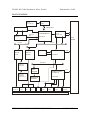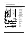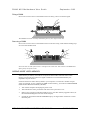
1
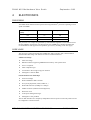
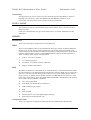
MOTHERBOARD DIVISION
User Guide
PH440 NLX Motherboard
www.mitsubishi-motherboard.com
124577UG September 1998
PH440 NLX Motherboard User Guide
September 1998
Document History
Issue
Description
Date
1.0
Preliminary
May 98
1.1
Update for production motherboards
July 98
1.2
Style update, added installation and upgrade guides
September 98
Trademarks mentioned within this document are the properties of their respective
owners. Details available on request.
Information contained in this document is subject to change without notice and does not
represent a commitment on the part of Mitsubishi Electric Motherboard Division.
No part of this manual may be reproduced or transmitted in any form or by any means
electronic or mechanical including photocopying and recording, for any purpose, without
the express written permission of the publishers.
Published by:
Mitsubishi Electric
Motherboard Division
3500 Parkside
Birmingham Business Park
Birmingham, England
B37 7YS
MITSUBISHI ELECTRIC MOTHERBOARD DIVISION
PAGE 2 OF 51
PH440 NLX Motherboard User Guide
September 1998
SAFETY AND REGULATORY NOTICES
GENERAL
Battery
This product contains a lithium battery.
Do not use a metal or other conductive implement to remove the battery. If a short-circuit is
made between its positive and negative terminals the battery may explode.
Replace a discharged battery with one of the same type; another type may explode or ignite.
Follow the instructions contained in the User Guide to replace the battery. Dispose of a
discharged battery promptly and in accordance with the battery manufacturer’s recommended
instructions. Do not recharge, disassemble or incinerate the discharged battery. Keep away from
children.
Anti-static precautions
Warning
Static electricity can cause permanent damage to electronic components. You should be
aware of this risk, and take precautions against the discharge of static electricity.
This product is at risk from static discharge because the electronic components of the
motherboard are exposed. Memory modules and replacement processors are examples of
electrostatic sensitive devices (ESSDs).
All work that involves contact with the PH440 NLX Motherboard should be done in an area
completely free of static electricity. We recommend using a Special Handling Area (SHA) as
defined by EN 100015-1: 1992. This means that working surfaces, floor coverings and chairs
must be connected to a common earth reference point, and you should wear an earthed wrist
strap and anti-static clothing. It is also a good idea to use an ionizer or humidifier to remove
static from the air.
Handle static-sensitive items with extreme care. Hold add-on components only by their edges,
avoiding their electrical contacts. In general, do not handle static-sensitive items unnecessarily.
Keep all conductive material, and food and drink, away from your work area and PH440 NLX
Motherboard.
LEGALITIES
This product complies with the relevant clauses of the following European Directives (and all
subsequent amendments):
Low Voltage Directive
73/23/EEC
EMC Directive
89/336/EEC
CE Marking Directive
93/68/EEC
Important
This product, when supplied, complies with the CE Marking Directive and its strict legal
requirements. Use only parts tested and approved by Mitsubishi Electric Motherboard
Division.
MITSUBISHI ELECTRIC MOTHERBOARD DIVISION
PAGE 3 OF 51
PH440 NLX Motherboard User Guide
September 1998
STANDARDS
Safety
This product complies with the American Safety Standard UL1950.
Electro-magnetic Compatibility (EMC)
This product complies with the following European EMC standards:
Emissions
EN50022 Class B
Immunity
EN50082-1 Class B
This product also complies with the following American EMC standard:
FCC Class B
FCC Compliance Statement
Note: This equipment has been tested and found to comply with the limits for a Class B digital
device, pursuant to part 15 of the FCC Rules. These limits are designed to provide reasonable
protection against harmful interference in a residential installation. This equipment generates,
uses and can radiate radio frequency energy and, if not installed and used in accordance with the
instructions, may cause harmful interference to radio communications. However, there is no
guarantee that interference will not occur in a particular installation. If this equipment does cause
harmful interference, which can be determined by turning the equipment off and on, the user is
encouraged to try to correct the interference by one or more of the following measures:
♦
Reorient or relocate the receiving antenna.
♦
Increase the separation between the equipment and receiver.
♦
Connect the equipment into an outlet on a circuit different to that which the receiver is
connected.
♦
Consult the dealer or an experienced radio/TV technician for help.
Important
You are cautioned that any change or modification to the product not expressly approved by
the manufacturer could void the approvals held by this product.
MITSUBISHI ELECTRIC MOTHERBOARD DIVISION
PAGE 4 OF 51
PH440 NLX Motherboard User Guide
September 1998
CONTENTS
1
Overview
8
Motherboard Features ...................................................................................................................... 9
Configuration Options ................................................................................................................... 10
Build-time ................................................................................................................................ 10
User Configurable .................................................................................................................... 10
Block Diagram............................................................................................................................... 11
2
Installation guide
12
3
Upgrading the motherboard
14
Adding more memory.................................................................................................................... 14
Fitting and removing DIMMs .................................................................................................. 14
Fitting a DIMM ........................................................................................................................ 15
Removing a DIMM .................................................................................................................. 15
Adding more video memory .......................................................................................................... 15
The processor assembly ................................................................................................................. 16
To fit a new processor .............................................................................................................. 17
Replacing the battery for the configuration CMOS ....................................................................... 18
4
Electronics
19
Processor........................................................................................................................................ 19
Core Logic ..................................................................................................................................... 19
Concurrency ............................................................................................................................. 20
Level 2 Cache ................................................................................................................................ 20
Memory ......................................................................................................................................... 20
Motherboard............................................................................................................................. 20
DIMM ...................................................................................................................................... 20
BIOS ........................................................................................................................................ 20
Configuration RAM ................................................................................................................. 20
Video ............................................................................................................................................. 21
VGA Controller........................................................................................................................ 21
AGP.......................................................................................................................................... 22
Audio ............................................................................................................................................. 23
ESS Solo 1 ............................................................................................................................... 23
Real Time Clock ............................................................................................................................ 23
Standard I/O................................................................................................................................... 24
MITSUBISHI ELECTRIC MOTHERBOARD DIVISION
PAGE 5 OF 51
PH440 NLX Motherboard User Guide
September 1998
Keyboard and Mouse ............................................................................................................... 24
Floppy Disk Interface............................................................................................................... 24
Serial Ports ............................................................................................................................... 24
Parallel Port.............................................................................................................................. 24
Additional I/O................................................................................................................................ 24
IDE Disk Controller ................................................................................................................. 24
Universal Serial Bus (USB) ..................................................................................................... 24
Security.......................................................................................................................................... 24
Motherboard Power ....................................................................................................................... 25
Processor Power ....................................................................................................................... 25
Battery...................................................................................................................................... 25
Power Management ....................................................................................................................... 25
Standby Switch......................................................................................................................... 25
Behaviour After AC-Disconnect .............................................................................................. 25
Sleep State Indication............................................................................................................... 25
System Management...................................................................................................................... 26
Heceta II System Monitor ........................................................................................................ 26
Fan Control .................................................................................................................................... 26
Expansion Slots ............................................................................................................................. 26
Industry Standard Architecture (ISA) ...................................................................................... 26
Peripheral Component Interconnect (PCI) ............................................................................... 26
Bus Resource Utilisation ............................................................................................................... 27
ISA DMA Channels ................................................................................................................. 27
ISA Interrupts........................................................................................................................... 27
PCI Interrupts ........................................................................................................................... 27
PCI Device Selection (motherboard devices)........................................................................... 28
PCI Arbitration......................................................................................................................... 28
5
BIOS Setup & POST
29
BIOS Setup .................................................................................................................................... 29
Control keys ............................................................................................................................. 29
Getting help in BIOS Setup...................................................................................................... 30
Reserving ISA legacy resources............................................................................................... 30
Multi-boot facility.......................................................................................................................... 30
Power-on self-test .......................................................................................................................... 31
Recoverable POST errors......................................................................................................... 31
Terminal POST errors and beep codes..................................................................................... 32
MITSUBISHI ELECTRIC MOTHERBOARD DIVISION
PAGE 6 OF 51
PH440 NLX Motherboard User Guide
6
Electrical
September 1998
39
Power Requirements ...................................................................................................................... 39
PCB................................................................................................................................................ 39
7
Connector Assignments
MITSUBISHI ELECTRIC MOTHERBOARD DIVISION
40
PAGE 7 OF 51
PH440 NLX Motherboard User Guide
1
September 1998
OVERVIEW
PH440 NLX is a Pentium II® processor-based NLX profile motherboard.
The design of PH440 NLX is based around the following components.
♦
Intel Pentium II® processor in Slot 1.
♦
Intel 440BX host bridge and system controller.
♦
Intel PIIX4e ISA bridge and peripheral and power management controller.
♦
SMSC 37C677 I/O Combo.
♦
ATI AGP 3D Rage Pro AGP or 3D Rage IIC AGP video controller with SGRAM frame
buffer.
♦
ESS Solo 1 audio controller.
®
Pentium II Processor
The Pentium® II processor adds MMX technology to the P6 micro-architecture in a cartridge
package which also includes a second-level cache. The cartridge plugs into a 242-pin slot
connector (slot 1) on the motherboard and operates at speeds from 233MHz.
440BX North bridge
The 440BX North bridge connects the processor to the SDRAM main memory, an AGP port and
PCI bus interface. The device is housed in a 492-pin BGA package.
PIIX4e ISA bridge
The PIIX4e provides the PCI to ISA bus bridge and contains the system’s RTC, the IDE
interfaces, the DMA and Interrupt Controllers. The PIIX4e also provides ACPI support, an
SMbus controller and all the general purpose I/O ports used on the PH440 NLX motherboard.
The PIIX4e device is packaged in a 324 pin BGA.
MITSUBISHI ELECTRIC MOTHERBOARD DIVISION
PAGE 8 OF 51
PH440 NLX Motherboard User Guide
September 1998
MOTHERBOARD FEATURES
Form factor
NLX, 9.0" wide x 11.2" long
Processor
Slot 1 with the VRM8.2 regulator on motherboard.
Accepts all Pentium II® (100MHz bus) processors
Core logic
Intel 440BX & PIIX4e
Cache
L2 cache included on processor module.
Memory –
RAM
3 DIMM sockets to accept 168 pin un-buffered PC100 SDRAM modules.
Memory Flash ROM
2Mb flash ROM. Includes BIOS, Setup-in-ROM, VGA, USB, DMI,
120MB floppy etc.
Buses
Supports 4 bus-master PCI slots and 5 ISA slots via riser.
VGA
AGP video via ATI Rage IIc or ATI Rage Pro.
64-bit or 72-bit ECC with 1-bit correct, 2-bit detect.
2 or 4MB SGRAM with upgrades via SODIMM module
Audio –
controller
Active speaker support only (external). Internal mono speaker and PCB
mounted ‘beeper’. ESS Solo 1 CODEC.
Hard Disk &
CD-ROM
Dual UltraDMA33 interfaces for hard disk and CD-ROM.
Floppy Disk
720kB, 1.2MB (3-mode), 1.44MB 3½ drives, 1.2MB 5¼ drives.
Support for 120MB drives via ATA port.
Parallel Port
IEEE 1284 (ECP & standard) on 25-way D-type
Serial Ports
Dual 16550s. Two 9-way D-types on rear edge of motherboard.
USB
Two ports. Two configurations available as build option. Either two ports
on rear panel or one on rear and second through NLX riser.
Keyboard &
Mouse
PS/2-style connectors. USB with legacy support
Security
Chassis intrusion detection via riser.
IR I/O
Optional through NLX riser (input only).
Power
Management
Green and deep green via system management mode.
ACPI compatible.
Requires logic-controlled PSU.
Standby option with wake-up on interrupt, serial port activity or button.
System
Management
Hardware monitoring (Voltage, temperature and fan monitor) via Heceta II
device.
Plug & Play
PC97 and PC98 compliant
Battery backup
On-board lithium coin cell with 5 years typical life.
PCB
4-layer NLX form-factor.
All components on top side
MITSUBISHI ELECTRIC MOTHERBOARD DIVISION
PAGE 9 OF 51
PH440 NLX Motherboard User Guide
September 1998
CONFIGURATION OPTIONS
Build-time
The following items can be configurable at build-time and cannot be modified by the user.
♦
Video controller (Rage IIc or Rage Pro).
♦
Video memory and upgrade socket.
♦
AMC connector.
♦
MIDI & joystick header.
♦
Heceta II system monitor.
♦
+5V supply to VGA connector pin 9.
♦
Dual rear USB or single rear and riser.
Contact Mitsubishi Electric Motherboard Division to determine available configurations.
User Configurable
The user can configure the following items.
♦
Processor (Intel boxed products)
♦
Main memory DIMMs
♦
Video memory upgrade (where available)
♦
Processor speed (core/bus ratio)
♦
BIOS ROM write enable
♦
Function enable/disable jumpers (audio CODEC, VGA)
MITSUBISHI ELECTRIC MOTHERBOARD DIVISION
PAGE 10 OF 51
PH440 NLX Motherboard User Guide
September 1998
BLOCK DIAGRAM
CORE VOLTAGE
DC-DC
CONVERTOR
SLOT1
CPU
HOST BUS
CLOCK BUFFER
82443BX
NORTHBRIDGE
MEMORY
BUS
MEMORY
DIMMS X 3
492 BGA
AGP BUS
ATI
RAGE
VGA
MOTHERBOARD
CLOCK
GENERATOR
NLX
RISER
PCI BUS
HECETA 2
ESS
SOLO1
AUDIO
PIIX4e
IDE
324 BGA
ISA BUS
VGA
MEMORY
SGRAMX2
XBUS
BUFFER
VGA
MEMORY
UPGRADE
SODIMM 144
VGA
OUTPUT
LINE
OUT
SMSC 37C67X
SUPER I/O
100 PQFP
BIOS ROM
TSSOP40
LINE
IN
MIC
IN
USB
FDC
SERIAL
COM2
SERIAL
COM1
PARALLEL
PORT
KEYBOARD
& MOUSE
REAR PANEL CONNECTORS
MITSUBISHI ELECTRIC MOTHERBOARD DIVISION
PAGE 11 OF 51
PH440 NLX Motherboard User Guide
2
September 1998
INSTALLATION GUIDE
Warning
Static electricity can cause permanent damage to electronic components. You should be
aware of this risk, and take precautions against the discharge of static electricity.
1
J9
3
2
4
1
3V Lithium cell
2
Processor socket
3
Processor fan power
4
Memory DIMMs
5
Multimedia upgrade
connector
6
Video memory
upgrade socket
7
ATAPI CD Audio
8
MIDI/joystick header
9
NLX riser connector
J1-4
Processor speed
selection
J5
Video enable jumper
J6
Motherboard audio
enable
J7
BIOS write protect
J8
Configuration
memory clear
J9
Motherboard
speaker enable
A
Line input
B
Microphone input
C
Line output
D
USB
E
Serial port 2
F
Keyboard
G
Mouse
H
Serial port 1
I
VGA monitor
J
Parallel port
J8
J7
J1
J2
J3
J4
9
5
J6
J5
8
7
6
J
G
A
B
C
D
E
F
H
I
MITSUBISHI ELECTRIC MOTHERBOARD DIVISION
PAGE 12 OF 51
PH440 NLX Motherboard User Guide
September 1998
Processor Core/Bus Ratio – J1-J4
J1
J2
J3
Ratio
Speed at
100MHz
3.5
350
X
4.0
400
X
4.5
450
X
X
J4
X
X
X
X – Jumper fitted
VGA Enable – J5
1-2
Disable on-board VGA controller
2-3
Enable on-board VGA controller
PCI Audio CODEC Enable – J6
1-2
Enable audio CODEC
2-3
Disable audio CODEC
BIOS Program Enable – J7
1-2
Disable BIOS updates
2-3
Enable BIOS updates
Clear Configuration (CMOS) Memory – J8
(Ensure AC is disconnected from the power supply before moving this jumper)
1-2
Normal operation
2-3
Clear CMOS (jumper must be returned to normal position before power-on)
Enable Motherboard Speaker – J9
1-2
Enabled
2-3
Disabled
MITSUBISHI ELECTRIC MOTHERBOARD DIVISION
PAGE 13 OF 51
PH440 NLX Motherboard User Guide
3
September 1998
UPGRADING THE MOTHERBOARD
Caution
Care must be taken in the purchase of upgrade parts to ensure both compatibility with the
system and the compliance with appropriate approvals and certification, e.g. CE marking
within Europe. Using non-approved parts may invalidate your warranty and system approvals.
Upgrading the motherboard is not difficult, but if you do not feel confident about the work
involved, you may wish to have your supplier or service organisation complete it for you.
Warning
Never carry out any work inside the computer with AC power applied. Turn off the computer
and unplug all power cords before starting work.
ADDING MORE MEMORY
The motherboard has three DIMM (Dual Inline Memory Module) sockets, each of which accepts
DIMMs of up to 128 Mbytes, in any combination. The slot furthest from the processor (MM1)
should be used first.
DIMM specification
The memory modules should meet the PC100 specification.
Fitting and removing DIMMs
Read all of these instructions through carefully before you start work.
Turn off the computer and unplug all power cords. Take suitable anti-static precautions and
remove the system cover. Leave the DIMM in the antistatic packaging until the last possible
moment and when you do take the DIMM out of its packaging, hold it by its ends and avoid
touching the metal contacts.
Follow the diagrams and simple instructions on the following pages to insert each DIMM.
Afterwards
After you have fitted new modules, check that the system recognises all the memory. If not,
check that you have:
♦
Correctly fitted the DIMMs in their slots.
♦
Installed DIMMs of the correct type.
It may be necessary to refit the original memory to check if there is a problem with your new
modules.
MITSUBISHI ELECTRIC MOTHERBOARD DIVISION
PAGE 14 OF 51
PH440 NLX Motherboard User Guide
September 1998
Fitting a DIMM
Do not use excessive force. If the module will not fit easily, remove it and start again.
The DIMM is inserted vertically and held in place by the clips at each end.
Removing a DIMM
Do not use excessive force. If the module will not come free easily, check that the holding clips
are clear of the module ends.
Press the tabs on both of the socket’s end clips at the same time. This releases the DIMM and
lifts it partly out of the socket.
ADDING MORE VIDEO MEMORY
Video memory is memory reserved for use by the on-board video controller. More video
memory can provide more colours or higher resolutions to an extent determined by the
capabilities of your monitor.
Check the amount of video memory fitted in your computer. You must fit a module of equal
value. For example, if your computer has 2MB of video memory, you must fit a 2MB SODIMM
(Small Outline Dual Inline Memory Module).
1.
Turn off the computer and unplug all power cords.
2.
Take suitable anti-static precautions and remove the system unit cover.
3.
Remove any expansion cards that impede access to the video memory upgrade socket (see
the motherboard diagram at the start of this chapter).
4.
Unpack the upgrade kit. Hold the SODIMM chip by its edges and be careful not to touch
the metal pins.
MITSUBISHI ELECTRIC MOTHERBOARD DIVISION
PAGE 15 OF 51
PH440 NLX Motherboard User Guide
September 1998
5.
Insert the SODIMM into the socket as shown in the illustration.
6.
Replace any expansion cards you removed earlier and refit the system unit cover.
You can now reconfigure your operating system to use the expanded capabilities of the video
controller.
THE PROCESSOR ASSEMBLY
To remove the existing processor
1.
Turn off the computer and unplug all power cords. Take suitable anti-static precautions and
remove the system cover.
2.
If the system was in use just before starting this procedure, the processor may be hot, wait
until it cools.
3.
If there are any expansion cards fitted that obstruct access to the processor, you may have to
remove them.
4.
See ‘A’ in the illustration. Carefully squeeze together the grips at both ends (1) of the
heatsink support bracket (2) and slide it away.
◊ Some designs of heatsink do not have this bracket fitted.
5.
See ‘B’ in the illustration. Press in the clips (1) at both ends of the top of the processor body
to depress the retaining pins out of the vertical supports. Then lift the processor body (2) out
of the socket.
Caution
Handle the processor with care, by the body only. Avoid touching the connector at the
bottom. Store in an antistatic container.
MITSUBISHI ELECTRIC MOTHERBOARD DIVISION
PAGE 16 OF 51
PH440 NLX Motherboard User Guide
September 1998
B
2
1
A
2
1
To fit a new processor
1.
Take the processor out of its anti-static packaging. Hold the processor by its edges, or its
heatsink and avoid touching the edge connector.
◊ The upgrade processor and the socket are keyed to ensure that the processor is installed in
the correct orientation. It will only fit into the socket one way.
2.
Slide the processor into the vertical guides and down into the socket, making sure that it is
correctly aligned and that you do not bend or otherwise damage the supports. Do not use
excessive force.
3.
Apply just enough pressure to overcome the resistance offered by the socket. Ensure that
the retaining pins snap into the sockets on the end supports.
4.
Refit the heatsink support, making sure that it is correctly and fully seated on the pins. It
should snap into place.
◊ This bracket may not be fitted with some heatsink designs, or may not be needed with the
new processor.
5.
The upgrade or overdrive processor may have its own cooling fan built into the heatsink.
This will have a power lead that will need to be connected to the processor fan power
(marked ‘3’ on the motherboard diagram, see installation guide).
◊ If the fan has only a two-pin connection, ensure it is connected to pins 1 and 2.
6.
Now adjust the processor multiplier speed jumpers on the motherboard (see installation
guide) in conjunction with the new processor’s data sheet.
Warning
The processor requires continuous airflow.
7.
Return to their original position any expansion cards that had been removed earlier, then
refit and secure the system cover.
MITSUBISHI ELECTRIC MOTHERBOARD DIVISION
PAGE 17 OF 51
PH440 NLX Motherboard User Guide
September 1998
REPLACING THE BATTERY FOR THE CONFIGURATION CMOS
The computer keeps a record of its current hardware configuration in a CMOS memory chip,
which is sustained by a small battery. This battery has a life of up to 5 years. If you find that you
have to reconfigure the computer every time you turn it on, or the date and time seem to be
dramatically incorrect, the battery is probably failing and needs to be replaced.
The battery is a 3-volt lithium type (CR2032 or equivalent) typically used in calculators, watches
and other small, battery-powered electronic items.
Read carefully the following instructions before commencing work.
1.
Turn off the computer and unplug all power cords.
Warning
Do not use a metal or other conductive implement to remove the battery. If a short-circuit is
accidentally made between its positive and negative terminals, it may cause the battery to
explode.
2.
Using a non-conductive implement, release the latch that holds the battery in place. The
battery will pop up allowing you to lift it out of the holder.
3.
Taking care not to touch the top or bottom surface of the new battery, pick up the
replacement with the positive (+) terminal upwards and press the battery into the holder
using a non-conductive implement.
4.
Dispose of the old battery in accordance with the battery manufacturer’s instructions.
When you next turn on the computer you will have to run the BIOS Setup utility to enter the
hardware configuration.
MITSUBISHI ELECTRIC MOTHERBOARD DIVISION
PAGE 18 OF 51
PH440 NLX Motherboard User Guide
4
September 1998
ELECTRONICS
PROCESSOR
The PH440 NLX motherboard accepts the following Pentium II® processors operating at a bus
speed of 100MHz.
Processor Speed
(MHz)
Core/bus ratio
Bus speed MHz
350
3.5
100
400
4.0
100
450
4.5
100
The processor core voltages are generated by switched-mode regulators on the motherboard to
the Intel VRM8.2 specification. The design meets the 100MHz Slot 1 flexible motherboard
recommendations and supports boxed products (processors), including a CPU fan supply.
CORE LOGIC
The core logic is based around the Intel 440BX PCI AGP Controller (PAC) and the PIIX4e
multi-function ISA bridge. The features of each are summarised below.
440BX Host bridge
♦
Slot1 host bridge
♦
DRAM controller supporting SDRAM main memory with optional ECC
♦
PCI 2.1 compliant
♦
AGP compliant target
♦
Virtual PCI to PCI bridge to support AGP bus
♦
Packaged in a 492 Pin BGA
PIIX4e Multifunction ISA Bridge
♦
PCI to ISA bridge
♦
Dual UltraDMA33 IDE controller
♦
ISA system peripherals (timers, DMA etc.)
♦
Dual USB controller (12Mbps or 1.5Mbps)
♦
SMbus controller (motherboard management)
♦
Real-time clock
♦
ACPI power management logic
♦
Packaged in a 324 pin BGA
The two IDE interfaces are completely independent and can operate concurrently. Both can also
be configured as a PCI bus master.
MITSUBISHI ELECTRIC MOTHERBOARD DIVISION
PAGE 19 OF 51
PH440 NLX Motherboard User Guide
September 1998
Concurrency
The major busses (processor, memory, PCI and AGP) all operate independently to achieve a
high degree of concurrency. Most CPU-DRAM and AGP-DRAM transfers can occur
concurrently with PCI transfers and so consume no PCI bus bandwidth.
LEVEL 2 CACHE
The second level cache is contained within the processor module. There is no provision for a
third level cache.
Cache size is determined by the type of CPU fitted, refer to your CPU manufacturer for this
information.
MEMORY
Motherboard
There is no main memory fitted directly to the motherboard.
DIMM
There are three DIMM sockets on the motherboards that accept 168-pin un-buffered SDRAM
modules to the PC100 memory module specification. All modules must support SPD (serial
presence detect) to allow the BIOS to determine the memory configuration and set up the chipset
optimally. These modules contain a small EEPROM that describes the module capabilities in
detail - including speed, capacity and organisation.
♦
64-bit or 72-bit (ECC) modules.
♦
2 or 4 bank organisation
♦
Asymmetric or symmetric memory addressing.
♦
Single or double-sided modules.
BIOS
The BIOS is contained in a flash ROM device soldered directly to the motherboard and includes
the code listed below. The motherboard will automatically perform a BIOS recovery operation if
it detects a valid recovery disk during the boot sequence. An override jumper that prevents all
writes (recovery or update) provides update protection. The BIOS ROM is accessed as a single
linear region in the memory space from 4GB-128kB (0FFFE0000 - 0FFFFFFFFh) and copied at
the top of ISA memory (0E0000 - 0FFFFFh).
♦
Core motherboard BIOS
♦
VGA BIOS (ATI RAGE PRO or RAGE IIC)
♦
USB, including legacy support
♦
DMI
♦
Setup-in-ROM
♦
Intel Pentium II® microcode update support and code
♦
Power and system management code
Configuration RAM
There is no support for configuration RAM other than the CMOS RAM within the RTC.
MITSUBISHI ELECTRIC MOTHERBOARD DIVISION
PAGE 20 OF 51
PH440 NLX Motherboard User Guide
September 1998
VIDEO
VGA Controller
The VGA controller is an ATI Rage Pro or ATI Rage IIC device packaged in a 256 ball BGA.
Video memory is via 2 SGRAM devices mounted on the motherboard (to give 2MB or 4MB)
and an SODIMM connector that accepts SGRAM modules (2MB or 4MB extra). The VGA
controller can be disabled via a motherboard jumper. It also provides an I2C bus to access other
video features. The VGA controller has the following features.
♦
AGP compliant to 133MHz (66MHz option).
♦
230MHz integrated RAMDAC.
♦
100MHz 64-bit SGRAM video memory (800MBps).
♦
DDC1, DDC2B, DPMS and Energy Star.
♦
2D acceleration.
♦
3D acceleration with triangle setup engine and texture cache (Rage Pro only).
♦
Motion video acceleration with MPEG2 assist.
♦
Multimedia channel for upgrades (AMC connector).
The allowable memory upgrade paths are shown in the table below. The entries are the total
memory capacity available by fitting 2MB or 4MB modules.
Motherboard
Memory1
2MB SODIMM
4MB SODIMM2
0MB
2MB
4MB
2MB
4MB
4MB
8MB
The amount of video memory fitted to the motherboard is automatically detected by the BIOS.
Video memory upgrade modules do not require an SPD ROM.
1
2MB builds are based on 8Mb devices. 4MB builds use 16Mb devices.
2
4MB modules must be based on 16Mb devices.
MITSUBISHI ELECTRIC MOTHERBOARD DIVISION
PAGE 21 OF 51
PH440 NLX Motherboard User Guide
September 1998
3
2D Display modes and maximum frame rates
256 colours
65536 colours
16.7M colours
2MB
2MB
4MB
2MB
4MB
640 x 480
200
200
200
200
200
800 x 600
200
200
200
160
160
1024 x 768
150
150
150
120
1152 x 864
120
120
120
85
1280 x 1024
100
100
85
1600 x 1200
76
76
Frame
Buffer
MB
Screen
Resolution
Colour
Depth
Bits/pixel
Display
Buffer4
MB
Z Buffer
Texture
Memory5
MB
2
512 x 384
16
0.38 x 2
0.38
0.88
2
640 x 480
16
0.59 x 2
0.59
0.24
4
640 x 480
16
0.59 x 2
0.59
2.24
4
640 x 480
32
1.17 x 2
0.59
1.07
4
800 x 600
16
0.92 x 2
0.92
1.25
8
1024 x 768
32
3.00 x 2
1.50
0.50
8
1280 x 1024
16
2.50 x 2
2.50
0.50
AGP
The Accelerated Graphics Port (AGP) is hardware interconnect designed to improve the
performance of 3D graphics displays. The specification is based on PCI but is point-to-point and
provides for data rates over 500MBps. The implementation on this motherboard is a private local
bus between the chipset and the Rage Pro video controller. The bus can operate in 1X or 2X
modes as defined by the AGP specification. When a Rage IIc device is fitted the interface
between the 443BX North Bridge and the VGA controller operates as a 66MHz PCI bus and no
AGP signalling occurs.
Two levels of performance gain are achieved:
♦
2D Operation. Since the AGP operates at 66MHz, twice the data rate of the PCI bus is
available to normal video traffic.
♦
3D Operation (Rage Pro only). Address translation logic and 133MHz bus mastering
allows the video controller to maintain texture information in main memory - reducing the
need for a large frame buffer.
3
These are the primary display modes. Others are available.
4
Front and back buffers.
5
Main memory can be used for additional texture storage via AGP.
MITSUBISHI ELECTRIC MOTHERBOARD DIVISION
PAGE 22 OF 51
PH440 NLX Motherboard User Guide
September 1998
AUDIO
The audio subsystem is based around an ESS Solo1 CODEC. The audio subsystem can be
completely depopulated to leave the standard PC beep function.
ESS Solo 1
♦
PCI bus interface
♦
Internal FM synthesiser
♦
Dual DMA support with FIFO & full duplex operation
♦
Programmable power management
♦
Joystick and MPU-401 compatible MIDI interfaces
♦
5 channel input mixer
One power amplifier is used - a National Semiconductor LM4880 ’Boomer’ to drive the LINEout jack socket and the optional internal speaker (via the NLX riser). The microphone input
provides power to enable condenser microphones to be used.
Channel
CODEC LINE
Rear line input jack socket
CODEC AUXA
CD input (from riser) or from motherboard connector
CODEC AUXB
VGA AMC Connector
CODEC MIC
Rear microphone jack socket or Riser connection
CODEC Mono In
Modem in audio from Riser
The following audio connectors are supported.
♦
Rear 3.5mm jack microphone input with phantom power
♦
Rear 3.5mm jack LINE in
♦
Rear 3.5mm jack LINE out
♦
Internal CD-ROM stereo audio on 4-pin ATAPI connector
♦
AMC connector stereo audio
♦
Modem audio via NLX riser auxiliary edge connections
REAL TIME CLOCK
The real time clock is located in the PIIX4e and includes 256 bytes of battery backed RAM with
two lockable ranges. The clock includes a date alarm and operates from a 32.768kHz crystal. The
3V lithium cell provides data retention for up to 5 years of normal use. Note that the battery is
used only when AC power is not applied to the system (or a standby 5V rail is not provided).
MITSUBISHI ELECTRIC MOTHERBOARD DIVISION
PAGE 23 OF 51
PH440 NLX Motherboard User Guide
September 1998
STANDARD I/O
The SMSC 37C677 Super IO controller provides standard I/O. This comprises the four functions
described below. It is packaged in a 100-pin PQFP and is PC98 and ACPI compliant.
Keyboard and Mouse
The keyboard and mouse controller uses the Phoenix Multikey version 1.40 firmware. PS/2 style
keyboard and mouse ports are provided on the rear panel. The ports are interchangeable.
Floppy Disk Interface
Standard 2-mode and 3-mode 3½” drives are supported.
The floppy disk drive signals are routed from the motherboard to the NLX riser and the floppy
disk drive connector is mounted on the NLX riser.
As per the NLX specification, all floppy disk input signals to the motherboard must be pulled up
on the NLX riser.
Serial Ports
There are two standard COM ports, which are wired to two standard 9-way D-type connectors on
the rear panel. The maximum Baud rate is 115K bits per second.
Parallel Port
This is EPP 1.7/1.9 and IEE1284 (ECP) compliant and is compatible with a standard (output
only) PC parallel port as well as a bi-directional (PS/2 style) parallel port. There is a 25-way Dtype connector on the rear panel.
ADDITIONAL I/O
IDE Disk Controller
Two UltraDMA33 IDE ports are provided with the controller integrated into the PIIX4e. This
allows for a maximum of four drives to be connected - two to each port. Normally the primary
port would be used for hard disk drives and the secondary port for CD-ROM or DVD drives.
120MB floppy drives have IDE interfaces.
Both IDE controllers are independent and both can bus-master data into memory for improved
performance. UltraDMA33 drives have a theoretical maximum transfer rate of 33MBs-1. The
interfaces are also, of course, compatible with standard ATA drives.
Universal Serial Bus (USB)
The motherboard supports two USB ports with the controller integrated into the PIIX4e. The
motherboard has a build option of a dual USB connector at the rear or with a single on the rear
and with the second port routed to the NLX riser to cater for an optional front USB connector.
The standard build is with a dual USB connector at the rear.
SECURITY
There is chassis intrusion detection available on motherboards with the Heceta II fitted. This is
capable of detecting an intrusion even when AC is disconnected (the logic is powered from the
3V lithium cell).
MITSUBISHI ELECTRIC MOTHERBOARD DIVISION
PAGE 24 OF 51
PH440 NLX Motherboard User Guide
September 1998
MOTHERBOARD POWER
Processor Power
A voltage regulator conforming to the Intel VRM8.2 standard supplies power for the processor
core. The motherboard automatically selects the correct processor voltage.
Battery
An IEC-type CR2032 3V lithium coin cell and holder are fitted to the board. Note that when the
motherboard is powered off but the AC remains connected (the standby rail is active) the battery
is not used.
POWER MANAGEMENT
Standby Switch
The motherboard supports an ACPI-compliant standby switch for use with a soft-switch power
supply. The action of the switch is under a combination of hardware and software control and is
summarised in the table below. The motherboard will power off regardless of the state of
software if the switch is held down for more than 4 seconds.
State
Action after switch pressed
Standby (soft power off)
Machine powers up and executes POST
POST, DOS or APM O/S
Machine powers off into standby state
Behaviour After AC-Disconnect
The ‘Wake on AC connect’ BIOS option and the state of the lithium cell determine the
behaviour of the motherboard after an AC-disconnect. The table below describes this.
Conditions
Action on AC Reconnect
CMOS RAM cleared. This is the state of a
new motherboard before assembly. This also
occurs after battery removal or failure.
Motherboard waits for standby switch
to be pressed.
CMOS RAM not cleared and ‘Wake on AC
connect’ was set to ‘Enabled’.
Motherboard fully powers up without
intervention.
CMOS RAM not cleared and ‘Wake on AC
connect’ was set to ‘Disabled’. This is the
default state. Resume events will be lost if an
AC power failure occurs.
Motherboard waits for standby switch
to be pressed.
Sleep State Indication
Indication of system activity states is provided by the signal ‘STANDBY_LED#’ to the NLX
riser (pin B159). If this signal is asserted (low) then the system is in a power-managed state. The
implementation of coloured LEDs to indicate system power states is dependent on the NLX riser
used.
MITSUBISHI ELECTRIC MOTHERBOARD DIVISION
PAGE 25 OF 51
PH440 NLX Motherboard User Guide
September 1998
SYSTEM MANAGEMENT
There are three main elements to the system management hardware.
♦
A Heceta II system monitor
♦
The PIIX4e power management devices 9 and 10
♦
Processor thermal diode ADCs
Heceta II System Monitor
The Heceta II provides the system monitor functions as described below and is accessed via the
PIIX4e SMbus interface. It provides the following functions.
♦
Fan monitoring. The two inputs to the Heceta II device monitor the first two NLX
“fantach” signals.
♦
Monitoring of system +12V, +5V, +3.3V, CPU core, -12V and 2.5V power rails
♦
Monitoring of system temperature (actually the motherboard surface temperature)
♦
Monitoring of chassis intrusion (top cover)
FAN CONTROL
The NLX system fan is controlled by the motherboard such that it stops rotating when the system
is in ‘Suspend’ mode. As a build option, the PH440 NLX motherboard supports variable fan
speed control in which the speed of the fan is raised as the temperature of the processor
increases. This considerably reduces fan noise in normal operation.
The variable fan speed option can only be used with an ACPI-aware operating system (such as
Windows 98) and a 100MHz-bus Pentium® II processor.
EXPANSION SLOTS
The ISA and PCI expansion slots are located on the riser card. The ISA and PCI signals are
routed through an edge connector on one edge of the board which mates with the NLX riser.
As per the NLX specification, the motherboard requires that the PCI signals are correctly
terminated and pulled up on the NLX riser for the motherboard to operate properly.
Industry Standard Architecture (ISA)
A maximum of 5 ISA slots is supported via the NLX riser.
Peripheral Component Interconnect (PCI)
A maximum of 4 PCI cards is supported via the NLX riser, each with bus master support.
MITSUBISHI ELECTRIC MOTHERBOARD DIVISION
PAGE 26 OF 51
PH440 NLX Motherboard User Guide
September 1998
BUS RESOURCE UTILISATION
ISA DMA Channels
DMA
Data Width
Usual Assignment
Audio
0
8-bit
ISA card
option
1
8-bit
ISA card
default 8-bit
2
8-bit
Floppy disk controller
3
8-bit
ECP parallel port
4
-
DMAC daisy chain
5
16-bit
ISA card
6
16-bit
ISA card
7
16-bit
ISA card
option
Shaded areas indicate DMA channels not normally available on the ISA bus
ISA Interrupts
IRQ
Usual Assignment
Fixed?
PCI
IRQ0
System timer
YES
IRQ1
Keyboard
NO
IRQ2
IRQ8 - 15 Cascade
YES
IRQ3
Serial port 2
NO
X
IRQ4
Serial port 1
NO
X
IRQ5
ISA/PCI bus (Audio)
NO
X
IRQ6
Floppy disk
NO
X
IRQ7
Parallel port
NO
X
IRQ8
Real time clock
NO
IRQ9
ISA/PCI bus
X
IRQ10
ISA/PCI bus
X
IRQ11
ISA/PCI bus
X
IRQ12
PS/2 Mouse
NO
IRQ13
Floating point error
YES
IRQ14
Primary hard disk
If drive connected
X
IRQ15
Secondary hard disk
NO
X
X
The last column indicates which ISA interrupts PCI devices can be routed to.
PCI Interrupts
Channel
Device
INTA#
Slots
INTB#
Slots
MITSUBISHI ELECTRIC MOTHERBOARD DIVISION
PAGE 27 OF 51
PH440 NLX Motherboard User Guide
INTC#
Audio & Slots
INTD#
Video & slots
September 1998
PCI Device Selection (motherboard devices)
Function
number
Address
line
Function
0
Device
number
(decimal)
0
0
11
Host bridge
0
1
0
12
PCI to PCI bridge
0
6
0
17
PCI Audio CODEC
0
7
0
18
South bridge
0
7
1
18
IDE controller
0
7
2
18
USB controller
0
7
3
18
Power management &
SMbus controllers
1
06
0
16
AGP video controller
Bus
number
PCI Arbitration
PIIX4e request
level
Bus
Function
0
0
PCI slot 1
1
0
PCI slot 2
2
0
PCI slot 3
3
0
PCI slot 4
4
0
PCI audio CODEC
Note that the arbiter implements a round robin scheme and thus no request level has fixed
priority over another. The AGP video controller does not consume any PCI bandwidth and
competes for memory resource independently.
6
PCI to PCI bridges translate address lines from AD16. The host bridge translates
address lines from AD11.
MITSUBISHI ELECTRIC MOTHERBOARD DIVISION
PAGE 28 OF 51
PH440 NLX Motherboard User Guide
5
September 1998
BIOS SETUP & POST
BIOS (pronounced “bye-oss”) stands for ‘basic input/output system’. The BIOS mediates
between the computer’s hardware – the processor, memory, and so on – and its software – the
operating system and your programs. The BIOS program is kept in permanent, read-only
memory or ROM (although if necessary it can be upgraded by an authorised maintainer).
BIOS Setup is a helpful utility that forms part of the BIOS program. It allows you to view and
alter the computer’s hardware configuration. It is also used to configure various security and
power-saving options. Configuring the computer is necessary to ensure that the software you use
can recognise and exploit the hardware’s capabilities.
The current configuration is kept in a special area of memory, called CMOS memory, and
maintained by a battery so that the configuration is preserved even while the computer is switched
off.
Whenever the computer is turned on, the BIOS power-on self-test (POST) routine tests various
hardware components, including memory, and compares the actual configuration of the computer
with that recorded in permanent (CMOS) memory.
A configuration discrepancy could arise if you have just installed or removed a hardware option
(for example, if you have added or replaced an expansion card).
BIOS SETUP
To start the BIOS Setup utility:
1.
Turn on or restart your computer.
2.
When you see
‘Press <F2> to enter setup’
appear on the screen, press the F2 key.
3.
If you have previously defined a Supervisor password, you are prompted for it before BIOS
Setup starts.
Control keys
Use the keys listed in the legend bar at the bottom of the BIOS Setup screen to make your
selections or exit the current menu.
Sub-menus are marked by a pointer. To display a sub-menu, use the arrow keys to move the
cursor to the sub-menu you want, then press ENTER.
Changeable fields are enclosed in square brackets. To select an item, use the arrow keys to move
the cursor to the field you want. Then use the PLUS (+) and MINUS (–) keys to select a value for
that field.
Press
To
F1 or Alt-h
View a general help topic. Press esc to close the help window.
Esc
Exit the current menu.
Left or Right arrow
Select a different menu.
Up or Down arrow
Select fields on the current menu.
Plus (+) or F6 or Spacebar
Select the next value for the current field.
Minus (-) or F5
Select the previous value for the current field.
MITSUBISHI ELECTRIC MOTHERBOARD DIVISION
PAGE 29 OF 51
PH440 NLX Motherboard User Guide
September 1998
Press
To
Enter
Make a selection from the menu bar or enter a sub-menu.
Home or End
Move the cursor to the top or bottom of the current menu.
Page up or Page down
Move the cursor to the next or previous page of the current menu.
F9
Restore the default settings for the fields on the current menu.
F10
Save the changes you’ve made and exit from BIOS Setup.
Caution
The default BIOS settings may not be appropriate for your particular system. Make a note of
the current settings before pressing F9 or using the Load Setup Defaults option of the Exit
menu.
Getting help in BIOS Setup
You can at any time get general help about the control keys by pressing the F1 key.
The help window on the right-hand side of each menu displays help text for the currentlyselected field. It changes as you move the cursor from one field to another.
Reserving ISA legacy resources
To reserve interrupts and upper memory block (UMB) regions for ISA expansion cards, go to the
Advanced menu, select PCI Configuration, then select PCI/PNP ISA IRQ Resource
Exclusion or PCI/PNP ISA UMB Region Exclusion as required.
MULTI-BOOT FACILITY
Immediately after the first screen, a second screen displays various POST messages such as the
memory test. While this screen is on display, a message at the bottom says: ‘Press <F2> to
enter setup or <ESC> to enter Boot Menu’. Even if this message is not displayed, you
can press the <ESC> key and this menu will appear just before booting:
Boot Menu
1.
2.
3.
4.
5.
Diskette Drive
Removable Devices
Hard Disk Drive
ATAPI CD-ROM Drive
Network Boot
< Enter Setup>
This menu can be used to temporarily use another drive or device to boot your system, for
example a bootable CD-ROM, without having to enter the BIOS setup. Simply use the up and
down arrows to make a selection. This change will not be permanent and the system boot will
revert to the normal BIOS setting the next time you switch on your system.
MITSUBISHI ELECTRIC MOTHERBOARD DIVISION
PAGE 30 OF 51
PH440 NLX Motherboard User Guide
September 1998
POWER-ON SELF-TEST
Recoverable POST errors
Whenever a recoverable (non-terminal) error occurs during POST, the BIOS displays an error
message describing the problem (the most usual are described below). After some messages, you
may be prompted to Press <F1> to resume, <F2> to enter Setup or just Press
<F2> to enter Setup.
In general, you should respond to these errors as follows:
♦
Shut down the computer, wait 20 to 30 seconds, and then turn it on again to see if the
problem is still reported.
♦
Check that all external cables are securely connected.
♦
Try running the BIOS Setup utility to reconfigure the system. If the computer will not
BOOT after you make changes in BIOS Setup, try returning to the original settings.
♦
Open up the system unit and check that all internal signal and power cables are securely
connected.
♦
If the problem persists, contact your supplier or authorised maintainer.
System Configuration Data updated
This message indicates that the system configuration has changed (such as an expansion
card has been added) and that the configuration data has therefore been updated.
System Configuration Data Write Error
This message indicates that the system configuration has changed (such as an expansion
card has been added) but the configuration data could not be updated. This is normally
caused by the BIOS program enable jumper being in the disable position. For configuration
changes to be correctly recorded the jumper must be in the enable position.
Invalid System Configuration Data – run configuration utility
The data describing the system configuration is incorrect and should be updated. This can
be done by checking the ‘Reset Configuration Data’ in BIOS Setup followed by ‘Save and
Exit’.
Diskette drive A error
Drive A: is present but fails the POST diskette tests. Check that the drive is defined
correctly in BIOS Setup. If necessary, open the system unit and check that the drive’s signal
(ribbon) cable is connected.
System/Extended/Shadow RAM failed at offset: xxxx Failing bits: yyyy
System, extended or shadow memory is not working, or not configured properly, at offset
xxxx. The hexadecimal number yyyy is a map of the bits at the address that failed the
memory test. Each “1” in the map represents a failed bit.
Fixed disk X failure or Fixed disk controller failure
A fixed (hard) disk drive is not working or not configured properly. Check that the drive is
defined correctly in BIOS Setup. If necessary, open the system unit and check that the
drive’s signal (ribbon) cable is connected.
Incorrect drive A type - run SETUP
The diskette drive is not correctly specified in BIOS Setup.
Invalid NVRAM media type
Problem with NVRAM (non-volatile random-access memory).
MITSUBISHI ELECTRIC MOTHERBOARD DIVISION
PAGE 31 OF 51
PH440 NLX Motherboard User Guide
September 1998
Keyboard error [nn] or Keyboard controller error
There is a problem with the keyboard or (less likely) the standard I/O controller on the
motherboard. If POST discovers a stuck key it displays its scan code.
Operating system not found
An operating system cannot be located either on a system diskette or on a hard disk. Start
BIOS Setup and check that the diskette and/or hard disk drives are specified correctly.
Parity check 1 xxxx or Parity check 2 xxxx
Parity error found on the system (1) or I/O (2) bus. The BIOS attempts to locate and display
the address xxxx. If it cannot locate the address, it displays “????”.
Previous boot incomplete - default configuration used
The previous POST did not complete successfully. POST loads default values and offers to
start BIOS Setup. If the failure was caused by incorrect values and they are not corrected,
the next boot will likely fail too.
Real-time clock error
Enter BIOS Setup and check the System Time and System Date settings on the Main menu.
System battery is dead - replace and run Setup
Replace the configuration battery as instructed in the previous chapter, then use BIOS
Setup to reconfigure the system.
System cache error - cache disabled
The RAM cache failed POST and BIOS disabled it.
System CMOS checksum bad - run Setup
System CMOS has been corrupted or modified incorrectly, perhaps by an application
program that changes data stored in CMOS. Run BIOS Setup and reconfigure the system
either by getting the default values or by making your own selections.
Terminal POST errors and beep codes
There are several POST routines that shut down the computer if they fail. If possible, the BIOS
sounds a sequence of beeps to identify the point at which POST failed. The most usual errors are
listed below.
The BIOS also issues one long tone followed by two short tones if the video system is faulty or if
an external ROM module (including video ROM) fails.
Turn off the computer for 30 seconds and then try again. If the fault persists, make a note of the
error code (if any) and call your supplier or authorised maintainer.
Beeps
Test which failed
1-2-2-3
1-3-1-1
1-3-1-3
1-3-4-1
1-3-4-3
1-4-1-1
2-1-2-3
2-2-3-1
1-2
BIOS ROM checksum
DRAM refresh.
8742 keyboard controller
RAM failure on address line.
RAM failure on data bits of low byte of memory bus.
RAM failure on data bits of high byte of memory bus.
Check ROM copyright notice
Test for unexpected interrupts
Video configuration failure, or option ROM checksum failure. (One long, two
short beeps.)
MITSUBISHI ELECTRIC MOTHERBOARD DIVISION
PAGE 32 OF 51
PH440 NLX Motherboard User Guide
September 1998
The BIOS also issues Port 80h codes that can be displayed using a suitable diagnostic card. The
codes can be used to determine the failure.
Code
POST Routine Description
02h
Verify Real Mode
03h
Disable Non-Maskable Interrupt (NMI)
04h
Get CPU type
06h
Initialise system hardware
08h
Initialise chipset with initial POST values
09h
Set IN POST flag
0Ah
Initialise CPU registers
0Bh
Enable CPU cache
0Ch
Initialise caches to initial POST values
0Eh
Initialise I/ O component
0Fh
Initialise the local bus IDE
10h
Initialise Power Management
11h
Load alternate registers with initial POST values
12h
Restore CPU control word during warm boot
13h
Initialise PCI Bus Mastering devices
14h
Initialise keyboard controller
16h
BIOS ROM checksum
17h
Initialise cache before memory autosize
18h
8254 timer initialisation
1Ah
8237 DMA controller initialisation
1Ch
Reset Programmable Interrupt Controller
20h
Test DRAM refresh
22h
Test 8742 Keyboard Controller
24h
Set ES segment register to 4 GB
26h
Enable A20 line
28h
Autosize DRAM
29h
Initialise POST Memory Manager
2Ah
Clear 512 KB base RAM
2Ch
RAM failure on address line
2Eh
RAM failure on data bits of low byte of memory bus
2Fh
Enable cache before system BIOS shadow
30h
RAM failure on data bits of high byte of memory bus
32h
Test CPU bus- clock frequency
33h
Initialise Phoenix Dispatch Manager
34h
Test CMOS RAM
35h
Initialise alternate chipset registers.
MITSUBISHI ELECTRIC MOTHERBOARD DIVISION
PAGE 33 OF 51
PH440 NLX Motherboard User Guide
September 1998
Code
POST Routine Description
36h
Warm start shut down
37h
Reinitialise the chipset (MB only)
38h
Shadow system BIOS ROM
39h
Reinitialise the cache (MB only)
3Ah
Autosize cache
3Ch
Advanced configuration of chipset registers
3Dh
Load alternate registers with CMOS values
42h
Initialise interrupt vectors
44h
Initialise BIOS interrupts
45h
POST device initialisation
46h
Check ROM copyright notice
48h
Check video configuration against CMOS
49h
Initialise PCI bus and devices
4Ah
Initialise all video adapters in system
4Bh
Display QuietBoot screen
4Ch
Shadow video BIOS ROM
4Eh
Display BIOS copyright notice
50h
Display CPU type and speed
51h
Initialise EISA board
52h
Test keyboard
54h
Set key click if enabled
56h
Enable keyboard
58h
Test for unexpected interrupts
59h
Initialise POST display service
5Ah
Display prompt "Press F2 to enter SETUP"
5Bh
Disable CPU cache
5Ch
Test RAM between 512 and 640 KB
5Eh
Base address
60h
Test extended memory
62h
Test extended memory address lines
64h
Jump to UserPatch1
66h
Configure advanced cache registers
67h
Initialise Multi Processor APIC
68h
Enable external and CPU caches
69h
Setup System Management Mode (SMM) area
6Ah
Display external L2 cache size
6Bh
Customise defaults
6Ch
Display shadow- area message
6Eh
Display possible high address for UMB recovery
MITSUBISHI ELECTRIC MOTHERBOARD DIVISION
PAGE 34 OF 51
PH440 NLX Motherboard User Guide
September 1998
Code
POST Routine Description
70h
Display error messages
72h
Check for configuration errors
74h
Test real- time clock
76h
Check for keyboard errors
77h
SMBus init devices
78h
Initialise system monitor and check for intrusion
79h
PCI audio init
7Ah
Test for key lock on
7Ch
Set up hardware interrupt vectors
7Eh
Initialise coprocessor if present
80h
Disable onboard Super I/ O ports and IRQs
81h
Late POST device initialisation
82h
Detect and install external RS232 ports
83h
Configure non- MCD IDE controllers
84h
Detect and install external parallel ports
85h
Initialise PC- compatible PnP ISA devices
86h
Re- initialise onboard I/ O ports.
87h
Configure Motheboard Configurable Devices
88h
Initialise BIOS Data Area
89h
Enable Non- Maskable Interrupts (NMIs)
8Ah
Initialise Extended BIOS Data Area
8Bh
Test and initialise PS/ 2 mouse
8Ch
Initialise floppy controller
8Eh
Autotype
8Fh
Determine number of ATA drives
90h
Initialise hard- disk controllers
91h
Initialise local- bus hard- disk controllers
92h
Jump to UserPatch2
93h
Build MPTABLE for multi- processor boards
95h
Install CD ROM for boot
96h
Clear huge ES segment register
97h
Fixup Multi Processor table
98h
Search for option ROMs. One long two short beeps on checksum failure
99h
Check for SMART Drive
9Ah
Shadow option ROMs
9Ch
Set up Power Management
9Dh
Security init
9Eh
Enable hardware interrupts
9Fh
Determine number of ATA and SCSI drives
MITSUBISHI ELECTRIC MOTHERBOARD DIVISION
PAGE 35 OF 51
PH440 NLX Motherboard User Guide
September 1998
Code
POST Routine Description
A0h
Set time of day
A2h
Check key lock
A4h
Initialise typematic rate
A8h
Erase F2 prompt
AAh
Scan for F2 key stroke
ACh
Enter SETUP
AEh
Clear IN POST flag
B0h
Check for errors
B1h
ROMPilot unload
B2h
POST done - prepare to boot operating system
B4h
One short beep before boot
B5h
Terminate QuietBoot
B6h
Check password (optional)
B7h
ACPI initialisation
B8h
Clear global descriptor table
B9h
Clean up all graphics
BAh
Initialise DMI parameters
BBh
Initialise PnP Option ROMs
BCh
Clear parity ch+ eckers
BDh
Display MultiBoot menu
BEh
Clear screen (optional)
BFh
Check virus and backup reminders
C0h
Try to boot with INT 19
C1h
Initialise POST Error Manager (PEM)
C2h
Initialise error logging
C3h
Initialise error display function
C4h
Initialise system error handler
C5h
Dual cmos init
C6h
Dock init
C7h
Dock init late
C8h
Force recovery check
C9h
Extended checksum check of bios
D2h
Unknown\unexpected interrupt
E0h
Initialise the chipset
E1h
Initialise the bridge
E2h
Initialise the CPU
E3h
Initialise system timer
E4h
Initialise system I/ O
E5h
Check force recovery boot
MITSUBISHI ELECTRIC MOTHERBOARD DIVISION
PAGE 36 OF 51
PH440 NLX Motherboard User Guide
Code
POST Routine Description
E6h
Checksum BIOS ROM
E7h
Go to BIOS
E8h
Initialise Multi Processor
E9h
Set Huge Segment
EAh
Initialilze OEM special code
EBh
Initialise PIC and DMA
ECh
Initialise Memory type
EDh
Initialise Memory size
EEh
Shadow Boot Block
EFh
System memory test
F0h
Initialise interrupt vectors
F1h
Initialise Run Time Clock
F2h
Initialise video
F3h
Initialise beeper
F4h
Initialise boot
F5h
Clear Huge segment
F6h
Boot to Mini DOS
F7h
Boot to Full DOS
MITSUBISHI ELECTRIC MOTHERBOARD DIVISION
September 1998
PAGE 37 OF 51
PH440 NLX Motherboard User Guide
September 1998
The following codes are produced during the BIOS recovery sequence.
Code
POST Routine Description
14h
Read file
16h
Erase sector
17h
Program sector
18h
Verify sector
E0h
Memory allocation error
E1h
File not found
E2h
Path not found
E3h
No handles available
E4h
Access denied
E5h
Invalid access code
E6h
Undefined file open error
E7h
Access denied on file read
E8h
Invalid handle
E9h
Undefined file read error
EAh
File close failure
EBh
Chip ID failure
ECh
Sector erase failure
EDh
Sector protect failure
EEh
Sector program failure
EFh
Sector verify error
88h
Video not found
FFh
Incorrect parameters
MITSUBISHI ELECTRIC MOTHERBOARD DIVISION
PAGE 38 OF 51
PH440 NLX Motherboard User Guide
6
September 1998
ELECTRICAL
POWER REQUIREMENTS
The motherboard power requirements are heavily dependent on system configuration and the
software being used. The table below can be used as a guide to the likely power supply
requirements. They are measured using a 400MHz Intel Pentium II® Processor, 3 memory
modules and 8MB video memory running stress test software designed to yield worst case
results. They should not, however, be regarded as maximum values.
Supply
+5V
standby
+5V
+3.3V
+12V
-12V
-5V
Voltage
Tolerance
± 5%
± 5%
± 3%
± 5%
± 5%
± 5%
Maximum
Current (in above
configuration)
20mA
5A
3A
300mA
100mA
100mA
Warning
Ensure that the system does not overload the +5V standby output of the power supply –
permanent damage to the motherboard may result.
This motherboard requires a +5V standby supply to operate correctly. This is normally
provided by an NLX-compatible power supply via the riser.
PCB
The PCB is a four-layer design measuring W9.0” x L11.2”. It is NLX compatible. The inner
power planes are arranged so that the ground plane is nearest the top component layer.
The PCB has a UL flammability rating of 94V-0.
MITSUBISHI ELECTRIC MOTHERBOARD DIVISION
PAGE 39 OF 51
PH440 NLX Motherboard User Guide
7
September 1998
CONNECTOR ASSIGNMENTS
Keyboard and Mouse (PS/2 Mini-DIN)
(Installation guide references F and G)
6
5
4
3
2
1
Pin
Signal
Direction
Description
1
CLK
I/O
Data clock
2
VCC
O
+5V Power
3
GND
-
Signal ground
4
NC
-
No connect
5
DATA
I/O
Serial data
6
NC
-
No connect
Serial Port 1 and Serial Port 2 (9 way D-type)
(Installation guide references E and H)
1
5
9
6
10101
Pin
Signal
Direction
Description
1
DCD
I
Data Carrier Detect
2
RXD
I
Receive Data
3
TXD
O
Transmit Data
4
DTR
O
Data Terminal Ready
5
GND
I
Signal ground
6
DSR
I
Data Set Ready
7
RTS
O
Request to Send
8
CTS
I
Clear to Send
9
RI
I
Ring Indicate
MITSUBISHI ELECTRIC MOTHERBOARD DIVISION
PAGE 40 OF 51
PH440 NLX Motherboard User Guide
September 1998
Parallel Port (25 way D-type)
(Installation guide reference J)
13
1
25
14
Pin
Standard mode
ECP mode
1
STB#
STB#
2
DATA0
DATA0
I/O
3
DATA1
DATA1
I/O
4
DATA2
DATA2
I/O
5
DATA3
DATA3
I/O
6
DATA4
DATA4
I/O
7
DATA5
DATA5
I/O
8
DATA6
DATA6
I/O
9
DATA7
DATA7
I/O
10
ACK#
ACK#
I
11
BUSY
BUSY
I
12
PE
PE
I
13
SLCT
SLCT
I
14
AFD#
AFD#
O
15
ERR#
ERR#
I
16
INIT#
INIT#
O
17
SLIN#
SLIN#
O
18
GND
GND
-
19
GND
GND
-
20
GND
GND
-
21
GND
GND
-
22
GND
GND
-
23
GND
GND
-
24
GND
GND
-
25
GND
GND
-
MITSUBISHI ELECTRIC MOTHERBOARD DIVISION
Direction
PAGE 41 OF 51
PH440 NLX Motherboard User Guide
September 1998
VGA (15 way high density D-type)
(Installation guide reference I)
1
5
6
10
15
11
Pin
Signal
Pin
Signal
1
Red
9
+5V Power (fused)
2
Green
10
GND
3
Blue
11
No Connect
4
No Connect
12
Monitor ID 1
5
GND
13
HSYNC
6
Red Return
14
VSYNC
7
Green Return
15
Monitor ID 3
8
Blue Return
USB Ports 0 and 1 (USB port 1 on the rear panel is an option)
(Installation guide reference D)
1
4
Port 1
Port 0
1
4
Pin
Signal
Direction
Description
1
VCC
O
+5V Power
2
DATA-
I/O
Differential Serial Data -
3
DATA+
I/O
Differential Serial Data +
4
GND
-
Signal ground
Line Input and Output (3.5mm stereo jack)
(Installation guide references A and C)
Pin
Signal
Sleeve
GND
Tip
Left channel
Ring
Right channel
MITSUBISHI ELECTRIC MOTHERBOARD DIVISION
PAGE 42 OF 51
PH440 NLX Motherboard User Guide
September 1998
Microphone Input (3.5mm stereo jack)
(Installation guide reference D)
Pin
Signal
Sleeve
GND
Tip
Mono input
Ring
Electret bias voltage
Processor Fan (3 way header with locking ramp)
(Installation guide reference 3)
Pin
Signal
Direction
Description
1
GND
-
Signal ground
2
+12V Power
O
DC fan drive voltage
3
FAN_TACH#
I
Tacho sense from fan
Internal CD audio (4 way ATAPI header)
(Installation guide reference 7)
Pin
Signal
Direction
Description
1
LEFT
I
Left audio input
2
GND
-
Signal ground
3
GND
-
Signal ground
4
RIGHT
I
Right audio input
MIDI/Joystick (16 way dual row header)
(Installation guide reference 8)
Pin
Signal
Pin
Signal
1
+5V Power
2
+5V Power
3
JAB1
4
JBB1
5
JACX
6
JBCX
7
GND
8
MIDI OUT
9
GND
10
JBCY
11
JACY
12
JBB2
13
JAB2
14
MIDI IN
15
+5V Power
16
Key
MITSUBISHI ELECTRIC MOTHERBOARD DIVISION
PAGE 43 OF 51
PH440 NLX Motherboard User Guide
September 1998
VESA/AMCC Support (40 way dual row header)
(Installation guide reference 5)
Pin
Signal
Pin
Signal
1
Digital GND
2
PIXEL DATA0
3
Digital GND
4
PIXEL DATA1
5
Digital GND
6
PIXEL DATA2
7
EVIDEO
8
PIXEL DATA3
9
ESYNC
10
PIXEL DATA4
11
EDCLK
12
PIXEL DATA5
13
SAD4
14
PIXEL DATA6
15
Digital GND
16
PIXEL DATA7
17
Digital GND
18
DCLK
19
Digital GND
20
SAD0
21
VFSENSE#
22
SAD1
2
23
I C CLOCK
24
SAD2
25
Key
26
Digital GND
27
Key
28
Key
29
+5V Power
30
SAD3
31
RESET#
32
SAD7
33
SAD6
34
SAD5
2
35
I C DATA
36
REV
37
Audio GND
38
+12V Power
39
Audio Right
40
Audio Left
MITSUBISHI ELECTRIC MOTHERBOARD DIVISION
PAGE 44 OF 51
PH440 NLX Motherboard User Guide
September 1998
NLX Riser Connector (Gold fingers) PCI Segment
(Installation guide reference 9)
Pin
Signal
Terminator
Pin
Signal
A1
A2
-12V
B1
PC_SPKR_RT
NC
B2
+12V
A3
A4
+12V
B3
PC_SPKR_LFT
NC
B4
+12V
A5
3.3V
A6
INTD#
B5
PCI_CLK0
B6
GND
A7
3.3V
A8
INTA#
RISER
B7
PCI_CLK1
B8
SER_IRQ
A9
INTB#
A10
PCI_CLK2
RISER
B9
PCI_INT2#
MB (series)
B10
3.3V
A11
+3.3V
A12
PCI_RST#
MB (series)
B11
B12
PCI_CLK3
GND
A13
PCI_GNT0#
RISER
B13
PCI_GNT3#
A14
PCI_CLK4
MB (series)
A15
GND
RISER
RISER
B14
3.3V
B15
PCI_GNT2#
B16
PCI_AD31
B17
PCI_REQ0#
Terminator
MB (series)
MB (series)
A16
PCI_GNT1#
A17
3.3V
A18
PCI_REQ2#
RISER
B18
GND
A19
PCI_REQ3#
RISER
B19
PCI_AD29
RISER (series)
A20
PCI_AD30
RISER (series)
B20
PCI_AD28
RISER (series)
A21
GND
B21
PCI_AD26
RISER (series)
A22
PCI_AD25
RISER (series)
B22
3.3V
A23
PCI_REQ1#
RISER
B23
PCI_AD24
A24
PCI_AD27
RISER (series)
A25
3.3V
A26
PCI_AD23
RISER (series)
B26
GND
A27
PCI_AD20
RISER (series)
B27
PCI_AD21
RISER (series)
A28
PCI_AD18
RISER (series)
B28
PCI_AD19
RISER (series)
A29
GND
B29
PCI_AD16
RISER (series)
A30
PCI_AD17
B30
3.3V
A31
PCI_IRDY#
B31
PCI_CBE2#
RISER (series)
B24
PCI_CBE3#
B25
PCI_AD22
A32
PCI_DEVSEL#
B32
PCI_FRAME#
A33
3.3V
B33
PCI_TRDY#
A34
PCI_STOP#
B34
GND
A35
PCI_PERR#
B35
PCI_SDONE
A36
PCI_SERR#
B36
PCI_LOCK#
A37
GND
B37
PCI_SB0#
A38
PCI_CBE1#
B38
3.3V
A39
PCI_AD13
RISER (series)
B39
PCI_AD15
A40
PCI_AD10
RISER (series)
B40
PCI_PAR
A41
GND
B41
PCI_AD14
A42
PCI_CBE0#
B42
GND
MITSUBISHI ELECTRIC MOTHERBOARD DIVISION
RISER (series)
RISER (series)
RISER (series)
RISER (series)
RISER (series)
PAGE 45 OF 51
PH440 NLX Motherboard User Guide
September 1998
NLX Riser Connector (Gold fingers) PCI Segment
(Installation guide reference 9)
Pin
Signal
Terminator
Pin
Signal
Terminator
A43
PCI_AD0
RISER (series)
B43
PCI_AD11
RISER (series)
A44
PCI_AD6
RISER (series)
B44
PCI_AD12
RISER (series)
A45
3.3V
B45
PCI_AD9
RISER (series)
A46
PCI_AD5
RISER (series)
B46
3.3V
A47
PCI_AD1
RISER (series)
B47
PCI_AD8
RISER (series)
A48
PCI_AD3
RISER (series)
B48
PCI_AD7
RISER (series)
A49
GND
B49
PCI_AD4
RISER (series)
A50
PCI_AD2
RISER (series)
B50
GND
A51
+5V
B51
PCI_PME#
MITSUBISHI ELECTRIC MOTHERBOARD DIVISION
MB 10k
3V3SBY
PAGE 46 OF 51
PH440 NLX Motherboard User Guide
September 1998
NLX Riser Connector (Gold fingers) ISA Segment
(Installation guide reference 9)
Pin
Signal
Terminator
Pin
Signal
ISA_RSTDRV
MB Series
B52
+5V
ISA_IOCHK#
MB 4k7 +5V
B53
ISA_IRQ9
A52
A53
A54
ISA_SD6
MB 10k +5V
B54
ISA_DRQ2
MB 5K6 GND
A55
ISA_SD7
MB 10k +5V
B55
ISA_SD3
MB 10k +5V
A56
ISA_SD4
MB 10k +5V
B56
ISA_OWS#
MB 1k +5V
A57
+5V
B57
ISA_SD1
MB 10k +5V
A58
ISA_SD2
MB 10k +5V
B58
ISA_AEN
A59
ISA_SD5
MB 10k +5V
B59
ISA_IOCHRDY
A60
ISA_SD0
MB 10k +5V
B60
ISA_SA18
MB 10k +5V
A61
ISA_SMEMW#
MB 10k +5V
B61
ISA_SMEMR#
MB 10k +5V
A62
ISA_SA19
MB 10k +5V
B62
ISA_SA16
MB 10k +5V
A63
ISA_IOW#
MB 10k +5V
B63
ISA_IOR#
MB 10k +5V
A64
ISA_SA17
MB 10k +5V
B64
ISA_DRQ3
MB 5k6 +5V
A65
GND
B65
ISA_SA15
MB 10k +5V
A66
ISA_DACK3#
B66
GND
A67
ISA_SA14
A68
ISA_DACK1#
MB 10k +5V
B67
ISA_SA13
B68
+5V
Terminator
MB 10k +5V
MB 1k +5V
MB 10k +5V
A69
ISA_DRQ1
MB 5k6 GND
B69
ISA_REFRESH#
MB 1k +5V
A70
ISA_SA12
MB 10k +5V
B70
ISA_SA11
MB 10k +5V
A71
ISA_SYSCLK
MB series
B71
ISA_SA10
MB 10k +5V
A72
ISA_SA9
MB 10k +5V
B72
ISA_IRQ7
MB 10k +5V
A73
+5V
B73
ISA_IRQ6
MB 10k +5V
A74
ISA_IRQ5
B74
ISA_SA8
MB 10k +5V
A75
ISA_SA7
MB 10k +5V
B75
ISA_SA6
MB 10k +5V
A76
ISA_IRQ3
MB 10k +5V
B76
IA_DACK2#
A77
ISA_IRQ4
MB 10k +5V
B77
ISA_SA4
A78
ISA_SA5
MB 10k +5V
B78
GND
A79
ISA_TC
A80
ISA_BALE
A81
GND
A82
MB 10k +5V
MB 10k +5V
B79
ISA_SA3
MB 10k +5V
MB 10k +5V
B80
ISA_SA2
MB 10k +5V
B81
ISA_SA1
MB 10k +5V
CLK14_ISA
MB series
B82
ISA_SA0
MB 10k +5V
A83
ISA_IOCS16#
MB 1k +5V
B83
ISA_SBHE#
MB 10k +5V
A84
ISA_MEMCS16
#
MB 1k +5V
B84
ISA_LA23
MB 10k +5V
A85
ISA_IRQ11
MB 10k +5V
B85
ISA_LA22
MB 10k +5V
A86
ISA_IRQ10
MB 10k +5V
B86
ISA_LA21
MB 10k +5V
A87
ISA_IRQ15
MB 10k +5V
B87
ISA_LA20
MB 10k +5V
A88
ISA_IRQ12
MB 10k +5V
B88
ISA_LA19
MB 10k +5V
A89
GND
A90
ISA_IRQ14
B89
ISA_LA18
MB 10k +5V
MB 10k +5V
B90
ISA_LA17
MB 10k +5V
A91
ISA_DRQ0
MB 5k6 GND
B91
ISA_DACK0#
A92
ISA_MEMR#
MB 10k +5V
B92
ISA_DACK5#
A93
ISA_MEMW#
MB 10k +5V
B93
ISA_SD8
MITSUBISHI ELECTRIC MOTHERBOARD DIVISION
MB 10k +5V
PAGE 47 OF 51
PH440 NLX Motherboard User Guide
September 1998
NLX Riser Connector (Gold fingers) ISA Segment
(Installation guide reference 9)
Pin
Signal
Terminator
Pin
Signal
A94
ISA_SD9
MB 10k +5V
B94
ISA_DACK6#
A95
ISA_DRQ5
MB 5k6 GND
B95
ISA_SD10
A96
ISA_DRQ6
MB 5k6 GND
A97
+5V
A98
ISA_SD12
A99
ISA_DACK7#
A100
ISA_SD14
A101
ISA_MASTER#
MB 10k +5V
B96
+5V
B97
ISA_SD11
Terminator
MB 10k +5V
MB 10k +5V
B98
ISA_DRQ7
MB 5k6 GND
B99
ISA_SD13
MB 10k +5V
MB 10k +5V
B100
ISA_SD15
MB 10k +5V
MB 330R +5V
B101
GND
MITSUBISHI ELECTRIC MOTHERBOARD DIVISION
PAGE 48 OF 51
PH440 NLX Motherboard User Guide
September 1998
NLX Riser Connector (Gold fingers) IDE and Floppy Disk Interfaces (Installation
guide reference 9)
Pin
Signal
Terminator
Pin
Signal
A102
PIDE_D8
MB series 33R
B102
GND
A103
PIDE_RESET#
MB series 33R
B103
PIDE_D7
MB series 33R
A104
PIDE_D9
MB series 33R
B104
PIDE_D6
MB series 33R
A105
+5V
B105
PIDE_D5
MB series 33R
A106
PIDE_D4
MB series 33R
B106
PIDE_D11
MB series 33R
A107
PIDE_D10
MB series 33R
B107
PIDE_D12
MB series 33R
A108
PIDE_D3
MB series 33R
B108
GND
A109
PIDE_D13
MB series 33R
B109
PIDE_D14
MB series 33R
A110
PIDE_D1
MB series 33R
B110
PIDE_D2
MB series 33R
A111
GND
B111
PIDE_D0
MB series 33R
A112
PIDE_IOW#
MB series 33R
B112
PIDE_D15
MB series 33R
A113
PIDE_DREQ
MB series 82R
B113
PIDE_IOR#
MB series 33R
A114
PIDE_RDY
MB series 82R
B114
PCSEL
470R GND
A115
PIDE_DACK#
MB series 33R
B115
ISA_IRQ14
MB series 82R
A116
RSVD1
B116
+5V
A117
PIDE_DA2
MB series 33R
B117
PIDE_DA1
MB series 33R
A118
PIDE_CS1#
MB series 33R
B118
PIDE_DA0
MB series 33R
A119
+5V
B119
PIDE_CS3#
MB series 33R
A120
NC (PDASP#)
B120
SIDE_D8
MB series 33R
A121
SIDE_RESET#
MB series 33R
B121
SIDE_D7
MB 33R series
A122
SIDE_D9
MB series 33R
B122
GND
A123
SIDE_D6
MB series 33R
B123
SIDE_D10
A124
SIDE_D5
MB series 33R
B124
+5V
A125
SIDE_D11
MB series 33R
B125
SIDE_D4
MB series 33R
A126
SIDE_D12
MB series 33R
B126
SIDE_D3
MB series 33R
A127
GND
B127
SIDE_D13
MB series 33R
A128
SIDE_D2
MB series 33R
B128
SIDE_D14
MB series 33R
A129
SIDE_D15
MB series 33R
B129
SIDE_D1
MB series 33R
A130
SIDE_IOW#
MB series 33R
B130
SIDE_D0
MB series 33R
A131
SIDE_DREQ
MB series 82R
B131
SIDE_IOR#
MB series 33R
A132
SIDE_RDY
MB series 82R
B132
SCSEL
470R GND
A133
GND
B133
ISA_IRQ15
MB series 82R
A134
SIDE_DACK#
B134
SIDE_DA1
MB series 33R
A135
NC
B135
SIDE_DA2
MB series 33R
A136
SIDE_DA0
MB series 33R
B136
SIDE_CS3#
MB series 33R
A137
SIDE_CS1#
MB series 33R
B137
NC (SDASP#)
A138
NC (DRV2#)
B138
GND
A139
+5V
B139
FD_DRATE0
A140
NC
B140
FD_DSEL1#
A141
FD_DENSEL
B141
FD_DSEL0#
A142
FD_MOT0#
B142
FD_DIR#
A143
FD_INDEX#
B143
NC (MSEN1)
A144
FD_MOT1#
B144
GND
MB series 33R
MB 10k
MITSUBISHI ELECTRIC MOTHERBOARD DIVISION
Terminator
MB series 33R
PAGE 49 OF 51
PH440 NLX Motherboard User Guide
September 1998
NLX Riser Connector (Gold fingers) IDE and Floppy Disk Interfaces (Installation
guide reference 9)
Pin
Signal
A145
A146
Terminator
Pin
Signal
GND
B145
FD_WDATA#
FD_WGATE#
B146
FD_TRK0#
A147
FD_STEP#
B147
NC (MSEN0)
A148
FD_WPRT#
B148
FD_RDATA#
A149
FD_HDSEL#
B149
FD_DCHG#
MITSUBISHI ELECTRIC MOTHERBOARD DIVISION
Terminator
PAGE 50 OF 51
PH440 NLX Motherboard User Guide
September 1998
NLX Riser Connector (Gold fingers) Miscellaneous
(Installation guide reference 9)
Pin
Signal
Terminator
Pin
Signal
A150
SMBUS_DATA
MB 2K7 +3V3
B150
GND
A151
SMBUS_CLK
MB 2K7 +3V3
B151
NC (IRSL0)
A152
FANTACH1
MB 10K +12V
B152
NC (IRSL1)
A153
FANTACH2
MB 10K +12V
B153
NC (IRSL2)
A154
FANTACH3
B154
IO_IRTX
A155
IO_FANCTL
B155
IO_IRRX
A156
+5V
B156
NC (FPSLEEP)
A157
NLX_USBP1-
B157
FPRST#
A158
NLX_USBP1+
B158
GND
A159
PIIX_SBOC1#
B159
STANBY_LED#
A160
NC (USB2N)
B160
PSU_PWRGOOD
A161
NC (USB2P)
B161
COR_SBYBTN#
A162
NC (USB2OC#)
B162
PSU_ON#
A163
GND
B163
LAN_WAKE
A164
VBATNLX
B164
NC (LANLED)
A165
INTRUDE#
B165
NC (MDMWAKE#)
A166
MSG_LED#
B166
NC (1394PWR)
A167
NC (1394GND)
B167
NC (RSVD7)
A168
NC (RSVD4)
B168
NC (RSVD6)
A169
5VSBY
B169
NC (RSVD5)
A170
+3V3 (SENSE)
B170
NC (-5V)
MB 1M
(VBAT)
Terminator
MB 10K +5V
NLX Supplemental Connector
(Installation guide reference 9)
A170
+3V3 (SENSE)
X1
CD IN LEFT
Y1
B170
CD IN RIGHT
X2
AUDIO GND
Y2
AGND
X3
MIC IN
Y3
AUDIO 5V
X4
HEADPHONE OUT LEFT
Y4
HEADPHONE OUT RIGHT
X5
HEADPHONE SWITCH
Y5
MICROPHONE SWITCH
X6
VOL_DN#
Y6
VOL_UP#
X7
GND
Y7
NC
X8
NC
Y8
NC
X9
NC
Y9
GND
X10
NC
Y10
NC
X11
NC
Y11
NC
X12
AGND
Y12
NC
X13
MODEM MIC
Y13
MODEM SPEAKER
MITSUBISHI ELECTRIC MOTHERBOARD DIVISION
PAGE 51 OF 51