1
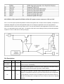
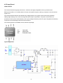
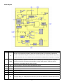
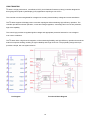
Service Manual
ViewSonic VX2413wm-2
Model No. VS12302
23.6” Color TFT LCD Display
(VX2413wm-2_SM Rev. 1a Apr. 2009)
ViewSonic 381 Brea Canyon Road, Walnut, California 91789 USA - (800) 888-8583
Copyright
Copyright © 2008 by ViewSonic Corporation. All rights reserved. No part of this publication
may be reproduced, transmitted, transcribed, stored in a retrieval system, or translated into any
language or computer language, in any form or by any means, electronic, mechanical, magnetic,
optical, chemical, manual or otherwise, without the prior written permission of ViewSonic
Corporation.
Disclaimer
ViewSonic makes no representations or warranties, either expressed or implied, with respect to
the contents hereof and specifically disclaims any warranty of merchantability or fitness for any
particular purpose. Further, ViewSonic reserves the right to revise this publication and to make
changes from time to time in the contents hereof without obligation of ViewSonic to notify any
person of such revision or changes.
Trademarks
Optiquest is a registered trademark of ViewSonic Corporation.
ViewSonic is a registered trademark of ViewSonic Corporation.
All other trademarks used within this document are the property of their respective owners.
Product disposal at end of product life
The lamp in this product contains mercury. Please dispose of in accordance with local, state or
federal laws.
Revision History
Revision
SM Editing Date
1a
04/24/2009
Description of Changes
Initial Release
2
TPV Model
Editor
TD9MNGNCYAVWAC
Eric
TABLE OF CONTENTS
1. Precautions and Safety Notices ......................................................................................... 4
2. Specification ....................................................................................................................... 7
3. Front Panel Function Control Description ....................................................................... 8
4. Circuit Description ............................................................................................................. 13
5. Adjusting Procedure .......................................................................................................... 21
6. Trouble Shooting Flow Chart ............................................................................................ 29
7. Block Diagrams ................................................................................................................ 30
8. Schematic Diagrams ........................................................................................................ 32
9. PCB Layout Diagrams ...................................................................................................... 41
10. Exploded Diagram and Spare Parts List ........................................................................ 46
11. Recommended Spare Parts List .................................................................................... 61
3
1. Precautions and Safety Notices
1.1 Safety Precautions
This monitor is manufactured and tested on a ground principle that a user’s safety comes first. However, improper
use or installation may cause damage to the monitor as well as the user. Carefully go over the following WARNINGS
before installing and keep this guide handy.
WARNINGS
.This monitor should be operated only at the correct power sources indicated on the label on the rear end of the
monitor. If you’re unsure of the power supply in your residence, consult you local dealer or power company.
.Use only the special power adapter that comes with this monitor for power input.
.Do not try to repair the monitor your self as it contains no user-serviceable parts. This monitor should only be
repaired by a qualified technician.
.Do not remove the monitor cabinet. There is high-voltage parts inside that may cause electric shock to human
bodies, even when the power cord is unplugged.
.Stop using the monitor if the cabinet is damaged. Have it checked by a service technician.
.Put your monitor only in a clean, dry environment. If it gets wet, unplug the power cable immediately and consult
your service technician.
.Always unplug the monitor before cleaning it .Clean the cabinet with a clean, dry cloth. Apply non-ammonia based
cleaner onto the cloth, not directly onto the glass screen.
.Keep the monitor away from magnetic objects, motors, TV sets, and transformer.
.Do not place heavy objects on the monitor or power cord.
1.2 Product Safety Notice
Many electrical and mechanical parts in this chassis have special safety visual inspections and the protection
afforded by them cannot necessarily be obtained by using replacement components rated for higher voltages,
wattage, etc. Before replacing any of these components read the parts list in this manual carefully. The use of
substitute replacement parts which do not have the same safety characteristics as specified in the parts list may
create shock, fire, or other hazards.
1.3 Service Notes
1. When replacing parts or circuit boards, clamp the lead wires around terminals before soldering.
2. When replacing a high wattage resistor (more than 1W of metal oxide film resistor) in circuit board, keep the
resistor about 5mm away from circuit board.
3. Keep wires away from high voltage, high temperature components and sharp edges.
4. Keep wires in their original position so as to reduce interference.
5. Usage of this product please refer to also user’s manual.
4
1.4 Handing and Placing Methods (Take VX2265wm for example)
Correct Methods:
Only touch the metal frame of the LCD panel or the
front cover of the monitor. Do not touch the surface of
the polarizer.
Take out the monitor
Place the monitor on a clean and soft foam pad.
Incorrect Methods:
Surface of the LCD panel is pressed by fingers and that
may cause “Mura.”
Taking out the monitor by grasping the LCD panel. That
may cause “Mura.”
Placing the monitor on foreign objects. That could
scratch the surface of the panel or cause “Mura.”
5
Place the monitor on the lap, the panel surface must
The panel is placed facedown on the lap. That may
be upwards.
cause “Mura.”
6
2. Specification
7
3. Front Panel Function Control Description
Use the buttons on the front control panel to display and adjust the OSD controls which display on the screen. The
OSD controls are explained at the top of the next page and are defined in “Main Menu Controls”.
8
Do the following to adjust the display setting:
1. To display the Main Menu, press button [1].
NOTE: All OSD menus and adjustment screens disappear automatically after about 15 seconds. This is adjustable
through the OSD timeout setting in the setup menu.
2. To select a control to adjust, press ▲ or ▼ to scroll up or down in the Main Menu.
3. After the desired control is selected, press button [2]. A control screen like the one shown below appears.
The line at the bottom of the screen
shows the current functions of buttons 1
and 2: Exit or select the Brightness
control.
4. To adjust the control, press the up ▲ or down ▼ buttons.
5. To save the adjustments and exit the menu, press button [1] twice.
The following tips may help you optimize your display:
• Adjust the computer's graphics card so that it outputs a 1920 x 1080 @ 60Hz video signal to the LCD display.
(Look for instructions on “changing the refresh rate” in the graphics card's user guide.)
• If necessary, make small adjustments using H. POSITION and V. POSITION until the screen image is completely
visible. (The black border around the edge of the screen should barely touch the illuminated “active area” of the LCD
display.)
9
Main Menu Controls
Adjust the menu items shown below by using the up ▲ and down ▼ buttons.
Control
Explanation
Auto Image Adjust automatically sizes, centers, and fine tunes the video signal to eliminate
waviness and distortion. Press the [2] button to obtain a sharper image.
NOTE: Auto Image Adjust works with most common video cards. If this function does not work on
your LCD display, then lower the video refresh rate to 60 Hz and set the resolution to its pre-set
value.
Contrast adjusts the difference between the image background (black level) and the foreground
(white level).
Brightness adjusts background black level of the screen image.
Audio Adjust
Volume increases the volume, decreases the volume, and mutes the audio.
Mute temporarily silences audio output.
Color Adjust provides several color adjustment modes, including preset color temperatures and
a User Color mode which allows independent adjustment of red (R), green (G), and blue (B). The
factory setting for this product is 6500K (6500 Kelvin).
sRGB-This is quickly becoming the industry standard for color management, with support being
included in many of the latest applications. Enabling this setting allows the LCD display to more
accurately display colors the way they were originally intended. Enabling the sRGB setting will
cause the Contrast and Brightness adjustments to be disabled.
9300K-Adds blue to the screen image for cooler white (used in most office settings with
fluorescent lighting).
7500K-Adds blue to the screen image for cooler white (used in most office settings with
fluorescent lighting).
6500K-Adds red to the screen image for warmer white and richer red.
5000K-Adds red to the screen image for warmer white and richer red.
User Color Individual adjustments for red (R), green (G), and blue (B).
1. To select color (R, G or B) press button [2].
2. To adjust selected color, press ▲ and ▼ .
Important: If you select RECALL from the Main Menu when the product is set to a Preset Timing
Mode, colors return to the 6500K factory preset.
10
Information displays the timing mode (video signal input) coming from the graphics card in the
computer, the LCD model number, the serial number, and the ViewSonic® website URL. See your
graphics card’s user guide for instructions on changing the resolution and refresh rate (vertical
frequency).
NOTE: VESA 1920 x 1080 @ 60Hz (recommended) means that the resolution is 1920 x 1080 and
the refresh rate is 60 Hertz.
Manual Image Adjust displays the Manual Image Adjust menu.
H./V. Position (Horizontal/Vertical Position) moves the screen image left or right and up or
down.
H. Size (Horizontal Size) adjusts the width of the screen image.
Fine Tune sharpens the focus by aligning text and/or graphics with pixel boundaries.
NOTE: Try Auto Image Adjust first.
Sharpness adjusts the clarity and focus of the screen image.
Dynamic Contrast allows the user to turn the contrast ratio enhancement on or off.
Aspect ratio Selects the image size for 4:3 and full screen.
ECO Mode provides the lower power consumption by reducing the brightness.
Standard: The default brightness setting.
Optimize: Decreases the brightness by 25 %.
Conserve: Decreases the brightness by 50 %.
Setup Menu displays the menu shown below:
11
Language Select allows the user to choose the language used in the menus and control screens.
Resolution Notice advises the optimal resolution to use.
OSD Position allows the user to move the OSD menus and control screens.
OSD Timeout sets the length of time the OSD screen is displayed. For example, with a “15
second” setting, if a control is not pushed within 15 seconds, the display screen disappears.
OSD Background allows the user to turn the OSD background On or Off.
Memory Recall returns the adjustments back to factory settings if the display is operating in a
factory Preset Timing Mode listed in the Specifications of this manual.
Exception: This control does not affect changes made with the User Color control, Language
Select or Power Lock setting.
12
4. Circuit Description
4.1 Main Board
NT68667UFG/C(U401)
The NT68167 is a highly integrated flat panel display controller that interfaces analog, digital, and video inputs. It
combines a triple ADC, a high quality zoom and shrink engine, a multi-color on screen display (OSD) controller and
many other functions in a single chip. It provides the user with a simple, flexible and cost-effective solution for
various flat panel display products.
The NT68167 operates at frequencies up to 166MHz , suitable for LCD monitor up to 1680x1050@75 resolution
and NT68167U operates at frequencies up to 190MHz , suitable for LCD monitor up to 1920x1080@75 resolution .
The NT68167 also has a built-in noise reduction function to provide more stable video quality, spread spectrum to
provide low EMI solution, sRGB for video color space convert and post pattern for manufacture test.
The display provided single/double pixel clock LVDS interface.
In addition, NT68167 includes an integrated 8-Bit Microcontroller (MCU). It contains an 8-bit 8031 micro-controller,
1,280-bytes internal data memory, four 7-bit resolution A/D Converter, 10-channel 8- bit resolution PWM DAC, and a
UART. Except those, it has one-channel hardware DDC solution, and VESA 2Bi/2B+ master/slave I2C bus interface.
Block Diagram
13
Pin Assignment
14
15
AP1117D33L (U701) and AP1117E18LA (U704): DC power convert, convert to 3.3V and 1.8V
AP1117 is a low dropout positive adjustable or fixed-mode regulator with 1A output current capability. The product is
specifically designed to provide well-regulated supply for low voltage IC applications such as high-speed bus
termination and low current 3.3V logic supply. AP1117 is also well suited for other applications such as VGA cards.
AP1117 is guaranteed to have lower than 1.4V dropout at full load current making it ideal to provide well-regulated
outputs of 1.25 to 5.0 with 6.4V to 18V input supply.
Pin Descriptions
Name
Adj (GND)
Vout
I/O
Pin #
I
1
O
2
Function
A resistor divider from this pin to the Vout pin and ground sets the output voltage.
(Ground only for Fixed-Mode)
The output of the regulator. A minimum of 10uF capacitor (0.15Ω ≤ESR ≤20Ω)
must be connected from this pin to ground to insure stability.
The input pin of regulator. Typically a large storage capacitor (0.15Ω ≤ESR
≤20Ω) is connected from this pin to ground to insure that the input voltage does
Vin
I
3
not sag below the minimum dropout voltage during the load transient response.
This pin must always be 1.3V higher than Vout in order for the device to regulate
properly.
16
4.2 Power Board
IC901 LD7576
The LD7576X series bring high performance, combines with highly integrated functions, protections and
EMI-improve solution. It’s an ideal solution for those cost-sensitive system, reducing component count and overall
system cost.
The LD7576X series features near-lossless high voltage startup circuit, green-mode power-saving operation,
leading-edge blanking of the current sensing and internal slope compensation. They also consist with more
protections of OLP (Over Load Protection), OVP (Over Voltage Protection) and OTP (Over Temperature Protection)
to prevent the circuit damage under abnormal conditions.
The LD7576X series are available in DIP-8 and SOP-8 package.
Typical Application
17
Block Diagram
Pin
Name
Function
This pin is to program the frequency of the low frequency timer. By connecting a capacitor to
1
CT
ground to set the OLP delay time. And this pin can be used for latch mode protection. By pulling
this pin lower than 0.8 V, the controller will be entered latch mode until the AC power-on recycling.
Voltage feedback pin (same as the COMP pin in UC384X), By connecting a photo-coupler to
2
COMP
close the control loop and achieve the regulation. A high quality ceramic capacitor (X7R) is
required for general applications (102pF at least).
3
CS
Current sense pin, connect to sense the MOSFET current
4
GND
Ground
5
OUT
Gate drive output to drive the external MOSFET
6
VCC
Supply voltage pin
7
NC
Unconnected Pin
Connect this pin to positive terminal of bulk capacitor to provide the startup current for the
8
HV
controller. When Vcc voltage trips the UVLO(on), this HV loop will be off to save the power loss on
the startup circuit.
18
IC801 TA9687GN
TA 9687 is a high performance, cost-effective CCFL (Cold Cathode Fluorescent Lamp) controller designed for
driving large-size Liquid Crystal Display (LCD) applications requiring 2 to 6 CCFLs.
The controller converts unregulated DC voltages into a nearly sinusoidal lamp voltage and current waveforms.
The TA 9687 supports full-bridge power conversion topologies while maintaining high-efficiency operation. The
controller provides a soft-start operation, current and voltage regulation, overvoltage and over-current protection,
high drive capability.
The control logic provides a regulated ignition voltage and appropriate protection features for over-voltage or
over-current conditions.
The TA 9687 offers a high level of integration, while maintaining flexibility and high-efficiency operation that reduces
external component heating, resulting in higher reliability and longer CCFL life. The proprietary design technique
provides a simple, low-cost system solution.
Pin Diagram
Functional Block Diagram
19
Pin Description
Pin No.
I/O1
Names
Description
1
I
VSEN
2
I/O
SSTCMP
3
I/O
CT
Timing Resistor and Capacitor for Operation and Striking Frequency
4
I/O
RT1
Timing Resistor for Striking Frequency
5
---
GNDA
Signal Ground
6
O
PDR2
High Side Driver Output 2
7
---
GNDP
Power Ground
8
O
NDR2
Low Side Driver Output 2
9
O
NDR1
Low Side Driver Output 1
10
O
PDR1
High Side Driver Output 1
11
---
VDDA
Input Power Pin
12
I/O
TIMER
Timing Capacitor for Delay Timer
13
I
PWM
External PWM Dimming Input
14
I
ISEN
Current Sense Feedback
15
I
OVPT
Over-Voltage Protection Threshold Voltage
16
I
ENA
Voltage Sense Feedback
Capacitor for Soft-Start and Loop Compensation
IC Enable/Disable
20
5. Adjustment Procedure
Setting the Timing Mode
Setting the timing mode is important for maximizing the quality of the screen image and minimizing eye strain. The
timing mode consists of the resolution (example 1920 x 1080) and refresh rate (or vertical frequency; example 60
Hz). After setting the timing mode, use the OSD (On-screen Display) controls to adjust the screen image.
For the best picture quality set your LCD display timing mode to:
VESA 1920 x 1080 @ 60Hz.
To set the Timing Mode:
1. Set the resolution: Right-click on the Windows desktop > Properties > Settings > set the resolution.
2. Set the refresh rate: See your graphic card's user guide for instructions.
WARNING: Do not set the graphics card in your computer to exceed the maximum refresh rate of 75Hz; doing so
may result in permanent damage to your LCD display.
OSD and Power Lock Settings
• OSD Lock: Press and hold [1] and the up arrow ▲ for 10 seconds. If any buttons are pressed the message OSD
Locked will display for 3 seconds.
• OSD Unlock: Press and hold [1] and the up arrow ▲ again for 10 seconds.
• Power Button Lock: Press and hold [1] and the down arrow ▼ for 10 seconds. If the power button is pressed the
message Power Button Locked will display for 3 seconds. With or without this setting, after a power failure, your
LCD display’s power will automatically turn ON when power is restored.
• Power Button Unlock: Press and hold [1] and the down arrow ▼ again for 10 seconds.
5.1 White balance, Luminance adjustment
Approximately 2 Hours should be allowed for warm up before proceeding White-Balance adjustment.
Before started adjust white balance, please setting the Chroma-C7120 MEM. Channel 0 to 9300K colors, MEM.
Channel 1 to 7500K colors, MEM. Channel 2 to 6500K MEM. Channel 3 to 5000K MEM. Channel 4 to sRGB
(our 9300K parameter is x=283±12, y=297±12 ; 7500K parameter is x=299±12, y=315±12 ;6500K parameter is x
=313±12, y=329±12; 5000K parameter is x = 347 ±12, y = 349 ±12; sRGB parameter is x=313±12, y=329±12)
How to setting MEM. channel you can reference to Minolta-CA210 user guide or simple use “ SC” key and “ NEXT”
key to modify x, y, Y value and use “ID” key to modify the TEXT description Following is the procedure to do
white-balance adjust
Enter into Burn/in mode:
AC ON the monitor with no signal ,and press “power” button to DC OFF the monitor, then press”1” and “power”
button at the same time to enter Burn/in mode;
Enter into the factory mode:
AC ON the monitor with signal connected, and press “power” button to DC OFF the monitor, then press”1” and
“power” button at the same time to enter factory mode;
21
Gain adjustment:
Move cursor to “Factory” and press “2” key.
Move cursor to “ Auto Level” and press “2” key to adjust Gain and Offset automatically;
(notice:this monitor do auto level must in T144(1280X1024@60Hz) P48(32 Grays))
a. Adjust sRGB (9300K) color-temperature
1. Switch the Chroma-C7120 to RGB-mode (with press “MODE” button)
2. Switch the MEM.channel to Channel 0 (with up or down arrow on Chroma-C7120)
3.The LCD-indicator on Minolta-CA210 will show x = 283 ±12, y = 297±12
b. Adjust Color1 (7500K) color-temperature
4. Switch the Chroma-C7120 to RGB-mode (with press “MODE” button)
5. Switch the MEM.channel to Channel 1 (with up or down arrow on Chroma-C7120)
6. The LCD-indicator on Minolta-CA210 will show x = 299 ±12, y = 315 ±12
c. Adjust Color2 (6500K) color-temperature
7. Switch the Chroma-C7120 to RGB-mode (with press “MODE” button)
8. Switch the MEM.channel to Channel 2 (with up or down arrow on Chroma-C7120)
9. The LCD-indicator on Minolta-CA210 will show x = 313 ±12, y = 329 ±12
d. Adjust sRGB (5000K) color-temperature
1. Switch the Chroma-C71200 to RGB-mode (with press “MODE” button)
2. Switch the MEM.channel to Channel 3 (with up or down arrow on Chroma-C7120)
3.The LCD-indicator on Minolta-CA210 will show x = 347 ±12, y = 360 ±12
e. Adjust sRGB (sRGB) color-temperature
1. Switch the Chroma-C7120 to RGB-mode (with press “MODE” button)
2. Switch the MEM.channel to Channel 4 (with up or down arrow on Chroma-C7120)
3.The LCD-indicator on Minolta-CA210 will show x = 313 ±12, y = 329 ±12
10. press “1” key to save adjust value and exit .
Turn the POWER-button off to on to quit from factory mode, and reset the monitor.
Max Brightness measurement: >250 cd/m2
Test conditions:
a. Switch to the full white pattern, in user mode main menu:
1. Set <Color Settings> Red, Green, and Blue to the max.
2. Set <Brightness> Brightness, Contrast to the max.
22
5.2 Firmware Upgrade Procedure
5.2.1 Equipment needed:
-
VX2413wm-2
-
PC (Personal computer)
-
LPT cable
-
Firmware upgrade program
ISP Board
LPT Cable
VGA Cable
23
Hardware Connect status
5.2.2 Update the NOVATEK’S firmware
You should jump the pin to “For Flash” at ISP Board
Connect to the
PC LPT
Connect to the VSC
VX2413wm-2
Double click “Writer.exe”
24
This tool can auto detect the right SCALAR programe speed,the process as follow:
When auto detect is finished,click “Load Hex”,then chosse the firmware that you want to update
25
Click “Auto”,then the update will begin.Wait for a moment until the bar is 100%,the program windows will show
“Programing Success”.This means the update is successful.
5.3 DDC Key in Procedure
Note:
1. Every time after replacing the main board, you have to do the DDC key in.
2. If you find the DDC does not conform to the LCD TV, you have to do the DDC key in.
5.3.1 Equipment Needed
-
VX2413wm-2
-
PC (Personal computer)
-
LPT cable
-
12V DC
-
Firmware upgrade program
-
DDC Card
5.3.2 Install software
You must install the
at the first.
Note: After installation, you must restart the PC to take the setup to effect.
26
5.3.3 Connect the DDC board as follow:
Connect to the
PC LPT
Connect this port to the
VSC VX2413wm-2’s VGA
12V Input
For analog
a. Double-click
,appear as follow Figs:
27
b. Click
.
c. Key in the Serial Number printed on the barcode label, then click “OK”
R9V090100001
12 codes,
for example.
d. Unit appears the following Fig, writer completed.
28
6. Troubleshooting Flow Chart
29
7. Block Diagram
7.1 Main Board
LCD Interface
(CN405)
FLASH MEMORY
Scalar IC NT68167
PM25LV020-100SCE
(Include MCU, ADC, OSD)
(U402)
(U401)
Crystal
12MHz
(X401)
DVI_SCL
DVI_SDA
Key Control
interface
(CN402)
EEPROM
M24C02
(U101)
H sync
D-DATA
V sync
D-CLK
RGB
D-Sub
Connector
(CN101)
30
7.2 Power Board
AC input
Bridge
Rectifier
and Filter
EMI filter
Transformer
Rectifier
diodes
Start Circuit: R904, R905
CN902
Feedback
Circuit
PWM Control
IC LD7576
5V
16V
ON/OFF
Output
Circuit
Lamp
Transformer
MOSFET
ON/OFF
Control
Feedback
Circuit
PWM Control
DIM
Over Voltage
31
8. Schematic Diagrams
8.1 Main Board
DSUB_5V
2.INPUT
3.SCALER
DSUB_5V
ESD_5V
BIN+
BINSOGI
GIN+
GINRIN+
RINHSIN
VSIN
DDC_SDA
ESD_5VDDC_SCL
+5V
VGA_DET
+5V
BIN+
BINSOGI
GIN+
GINRIN+
RINHSIN
VSIN
4.PANEL INTERFACE
BIN+
BINSOGI
GIN+
GINRIN+
RINHSIN
VSIN
DDC_SDA
DDC_SCL
VGA_DET
DDC_WP
PANEL_EN
PANEL_EN
T7P
T7M
TCLK1P
TCLK1M
T6P
T6M
T5P
T5M
T4P
T4M
T3P
T3M
T7P
T7M
TCLK1P
TCLK1M
T6P
T6M
T5P
T5M
T4P
T4M
T3P
T3M
DDC_SDA
DDC_SCL
VGA_DET
DDC_WP
INPUT
PANEL_EN
T7P
T7M
TCLK1P
TCLK1M
T6P
T6M
T5P
T5M
T4P
T4M
T3P
T3M
T2P
T2M
T1P
T1M
T0P
T0M
T2P
T2M
T1P
T1M
T0P
T0M
T2P
T2M
T1P
T1M
T0P
T0M
PANEL INTERFACE
5.POWER
DSUB_5V
5VCC
+5V
ESD_5V
VCC3.3
VCC3.3
Panel_ID#
+5V
BL_ADJ
5VCC
BL_ON
DSUB_5V
Volume#
Mute#
VCC1.8
Panel_ID#
BL_ADJ
VCC3.3
Panel_ID#
VCC3.3
BL_ADJ
BL_ON
BL_ON
Volume#
Mute#
+5V
+5V
Volume#
VCC1.8
Mute#
ESD_5V
VCC1.8
5VCC
VCC1.8
5VCC
POWER
SCALER
T P V ( Top
Victory
Electronics
Co . ,
Ltd. )
OEM MODEL
Viewsonic VX2413wm
Size
Rev
絬隔瓜絪腹
G3225-1-2-X-3-090330
TPV MODEL
CBPC9NGVWQ1
Key Component
1.0 Block Diagram
PCB NAME
715G3225-1-2
Date
Monday , March 30, 2009
32
Sheet
1
of
6
称爹
A
1
FB102
VGA_B+
H_Sy nc R101
0R05 1/10W 5%
V_Sy nc
R102
100R 1/16W 5%
R103
100R 1/16W 5%
1
BEAD
2
R104
100R 1/16W 5%
HSIN 5
R107
C102
22pF
R105
2K2 1/16W 5%
C103
33pF
2K2 1/16W 5%
R106
13
12
11
VGA_BVGA_B+
VGA_GVGA_G+
VGA_RVGA_R+
10K 1/16W 5%
VGA_G+
VGA_DET 5
1
BEAD
ZD103
RLZ5.6B
2
R112
ZD104
RLZ5.6B
R109
390 OHM 1/16W
C106
1000pF
SOGI 5
R111
100R 1/16W 5%
C107
0.047uF
GIN+ 5
R114
100R 1/16W 5%
C109
0.047uF
GIN- 5
R115
100R 1/16W 5%
C110
0.047uF
RIN+ 5
C113
0.047uF
RIN- 5
C118
NC
75R 1/16W 5%
VGA_G-
CN101
FB101
VGA_R+
D-SUB NC pin connect to GND
1
BEAD
2
R116
C119
NC
75R 1/16W 5%
VGA_R-
R117
100R 1/16W 5%
DSUB_5V
ESD_5V
U102
6
5
4
VGA_G+
ESD_5V 7
VGA_R+
AZC199-04S
R122
0R05 1/16W
+5V
5,6,7 +5V
C114
NC
1
I/O1 I/O4
GNDVDD
I/O2 I/O3
2
VGA_B+
1
2
3
D101
BAV70
ESD_5V
1
2
3
I/O1 I/O4
GNDVDD
I/O2 I/O3
6
5
4
AZC199-04S
H_Sy nc
R120 R121
V_Sy nc
C115
NC
DDC_SCL
DDC_SDA
5 DDC_WP
T P V ( Top
Electronics
U101
8
7
6
5
VCC A0
WP
A1
SCL A2
SDA VSS
M24C02-RMN6TP
Co . ,
Ltd. )
OEM MODEL
Viewsonic VX2413wm
Size
CBPC9NGVWQ1
Rev
絬隔瓜絪腹
G3225-1-2-X-3-090330
TPV MODEL
2.INPUT
PCB NAME
Monday , March 30, 2009
C116
0.22uF
1
2
3
4
Key Component
Date
33
Victory
R119
4K7 1/16W 5%
DSUB_SCL
4K7 1/16W 5%
DSUB_SDA
3
U103
4K7 1/16W 5%
5 DDC_SDA
100R 1/16W 5%
DSUB_SDA
BIN- 5
17
R113
R118
2
14
VGA_PLUG
DSUB_5V
C105
0.047uF
FB103
1
15
2
5 DDC_SCL
10
5
9
4
8
3
7
2
6
1
1
DB15
100R 1/16W 5%
DSUB_SCL
16
DSUB_5V
R110
R108
100R 1/16W 5%
NC
75R 1/16W 5%
DSUB_5V 7
BIN+ 5
C117
VSIN 5
VGA_B-
C101
0.047uF
Sheet
715G3225-1-2
3
of
6
称爹
B
1
FB404
120 OHM DVDD
VCC3.3
VCC3.3
C451
ADC_3.3 ADC_1.8
C431
0.1UF 16V
DVDD
14
15
4 HSIN
4 VSIN
T0M
T0P
T1M
T1P
T2M
T2P
TCLK1M
TCLK1P
T3M
T3P
T4M
T4P
T5M
T5P
T6M
T6P
T7M
T7P
HSY NCI1
VSYNCI1
VCC3.3
R408
NC
R405
R452
R449
C408
0.22uF16V
WP
SPI_SO
SPI_CE
100R 1/16W 5%
100R 1/16W 5%
100R 1/16W 5%
U402
1
2
3
4
PWMB*
PWMA*
NT68167UFG
CE# VDD
SO HOLD#
WP# SCK
GND
SI
8
7
6
5
R450
R451
4 DDC_SDA
4 DDC_SCL
SPI_CK
SPI_SI
100R 1/16W 5%
100R 1/16W 5%
17
16
PM25LV020-100SCE
R471
10K 1/16W 5%
SPI_CE
SPI_SI
SPI_SO
SPI_CK
62
61
60
59
PB5*/DDC_SDA*/TX
PB4*/DDC_SCL*/RX
R419
R463
R464
1K 1/16W 5%
NC
NC
R417
10K 1/16W 5%
C429
NC
U403
A0
A1
A2
GND
63
2
VCC
WP
SCL
SDA
C401
1
2
3
4
C411 47pF
0.1UF 16V
1
8
7
6
5
18
NC
X401
12MHz
SPI_CE
SPI_SI
SPI_SO
SPI_CLK
PA7*/PWM9*
PA6*/PWM8*
PA5*/PWM7*
PA4*/PWM6*
PA3/PWM5
PA2/PWM4
PA1/PWM3
PA0/PWM2
P35
P34
P31/TXD
P30/RXD
RSTB
PB3/ADC3
PB2/ADC2
PB1/ADC1
PB0/ADC0
OSCI
R462
1M 1/16W 5%
R429
T0M 6
T0P 6
T1M 6
T1P 6
T2M 6
T2P 6
TCLK1M 6
TCLK1P 6
T3M 6
T3P 6
T4M 6
T4P 6
T5M 6
T5P 6
T6M 6
T6P 6
T7M 6
T7P 6
52
29
7 VCC1.8
FB403
300OHM
ADC_1.8
C442
4.7uF/16V
C0805
C406
0.1UF 16V
CVDD_1.8
FB406
300OHM
DDC_WP 4
BL_ADJ 7
53
54
28
27
57
58
21
20
C443
4.7uF/16V
C0805
R414
R410
64
0R05 1/16W OSCO
VCC3.3 FB407
NC
Volume# 7
Mute# 7
EE_WP
C407
0.1UF 16V
ADC_3.3
Panel_ID# 7
WP
22K 1/16W 5%
22K 1/16W 5%
LEDB
LEDO
C439
NC
C0603
PANEL_EN 6
FB405
NC
5V_DET
55
56
23
22
C433
0.1UF 16V
CVDD_3.3
BL_ON 7
KEY 1
KEY 2
C445
+
NC
C444
0.1uF/16V
C410
0.1UF 16V
R473
key 1
3
13
24
50
C412 47pF
49
48
47
46
45
44
43
42
41
40
39
38
37
36
35
34
33
32
AGND
MGND
DGND
DGND
NC
NC
POWER_KEY #
MSCL
MSDA
VCC3.3
R455
EE_WP
MSCL
MSDA
R454
R453
NC
4 VGA_DET
4.7uF/16V
NT68167
VCC3.3
51
19
31
30
C430
26
CVDD_1.8
25
1
11
12
2
CVDD_2.3
BIN1+
BIN1SOG1I
GIN1+
GIN1RIN1+
RIN1-
ADC_1.8
4
5
6
7
8
9
10
BIN+
BINSOGI
GIN+
GINRIN+
RIN-
ADC_2.3
4
4
4
4
4
4
4
10UF6.3V
NC
DVDD_BIAS
DVDD
U401
C450
CVDD_3.3 CVDD_1.8
0R05 1/16W
key 2
CN401
key 3
key 4
1
2
3
4
5
6
7
8
R403
R404
VCC3.3
10K 1/16W 5%
R409
20K OHM 1/16W
+5V
R465
4K3 OHM 1/16W 5%
3
LEDO
CN408
7
6
5
4
3
2
1
1
2
3
4
5
6
7
NC
LED_GRN/BLUE
470R 1/16W 5%
R402
NC
R470
0R05 1/16W
+5V
LMBT3906LT1G
Q408
1
R469
LED_ORANGE
100R 1/10W 5%
FB410
GND
1
2
NC/BEAD
FB409
NC
C409 0.1UF 16V
FB407: 300 Ohm bead
FB405: 300 Ohm bead
C439,C444: 2.2uF
C445: NC (if ripple in spec)
FB403,FB406: 0 ohm
2
0.1UF 16V
R468
3K3 1/16W 5%
3
C415
0.1UF 16V
RLZ5.6B
C414
0.1UF 16V
D404
C413
RLZ5.6B
RLZ5.6B
0.1UF 16V
D405
C416
0.1UF 16V
D406
C417
CN407
R466
Inte. 1.8V
under
1920x1080
FB407: NC
FB405: NC
C439,C444: NC
C445: NC
FB403,FB406 300 ohm bead
DVDD
CONN
NC
100R 1/16W 5%
100R 1/16W 5%
5V_DET
0R05 1/16W
LMBT3906LT1G
Q407
1
R407
R416
R411
R428
R427
key 1
key 2
POWER_KEY #
LED_GRN/BLUE
LED_ORANGE
GND
R467
2
3.9K OHM 1/16W
3.9K OHM 1/16W
3.9K OHM 1/16W
7 VCC3.3
R406
LEDB
1
2
3
4
5
6
Ext. 1.8V
in
1920x1080
+5V 4,6,7
CN402
6
5
4
3
2
1
+5V
NC
NC
NC
CN406
R474
0R05 1/16W
TOUCH_PANEL 1
C404 NC
D402 NC
NC
VCC3.3
2
OEM MODEL
Viewsonic VX2413wm
Size
絬隔瓜絪腹
G3225-1-2-X-3-090330
TPV MODEL
CBPC9NGVWQ1
Rev
Key Component
3.SCALER
PCB NAME
T P V ( Top
Date
34
Victory
Electronics
Monday , March 30, 2009
Co . ,
Ltd. )
Sheet
715G3225-1-2
4
of
6
称爹
C
1
CN403
CN405
PANEL_VCC
FB408
T0M
T1M
T2M
TCLK1M
T3M
T4M
T5M
T6M
TCLK1M
T7M
R421
R434
C420
R1206 220 OHM 1/4W
R1206 220 OHM 1/4W
0.1UF 16V
120 OHM
2
4
6
8
10
12
14
16
18
20
22
24
26
28
30
T0P
T1P
T2P
TCLK1P
T3P
T4P
T5P
T6P
TCLK1P
T7P
R415
4K7 1/16W 5%
T4P
T4M
T3P
T3M
5
5
5
5
5
5
T2P
T2M
T1P
T1M
T0P
T0M
T5P
T5M
T4P
T4M
T3P
T3M
TCLK1P
TCLK1M
T2P
T2M
T1P
T1M
T0P
T0M
NC
5
6
7
8
3D
D
D
D
D
Q405
56K 1/16W 5%
AO3401
R418
NC
Q404
LMBT3904LT1G
C419
0.22uF16V
2
1
S
G
AO3401L
+5V
C441
0.1UF 16V
C421
1uF/16V
T P V ( Top
Victory
Electronics
Co . ,
Ltd. )
Viewsonic VX2413wm
Size
CBPC9NGVWQ1
Rev
G3225-1-2-X-3-090330
TPV MODEL
Key Component
4.PANEL INTERFACE
PCB NAME
Sheet
Monday , March 30, 2009
35
R420
10K 1/16W 5%
OEM MODEL
絬隔瓜絪腹
Date
Q403
NC
4
3
2
1
R436
22K 1/16W 5%
5
5
5
5
T7P
T7M
TCLK1P
TCLK1M
T6P
T6M
PANEL_VCC
R433
10K 1/16W 5%
R435
T7P
T7M
TCLK1P
TCLK1M
T6P
T6M
5 T5P
5 T5M
CONN
+5V
5 PANEL_EN
5
5
5
5
5
5
1
2
3
4
5
6
7
8
9
10
11
12
13
14
15
16
17
18
19
20
21
22
23
24
25
26
27
28
29
30
G
S
S
S
C449
100uF25V
+
1
3
5
7
9
11
13
15
17
19
21
23
25
27
29
715G3225-1-2
5
of
6
称爹
A
1
3
2
1
VIN
VOUT
ADJ(GND)
U701
AP1117D33L-13
+5V
CN404
4,5,6 +5V
5VCC
U702
NC
VIN VOUT(heat sink)
BKLT-VBRI
BKLT-EN
C_PANEL_INDEX
Volume
Mute
1
+5V
5,6,7
R702
VCC3.3
5VCC
VCC3.3 5
R701
NC
CONN
2
4
GND
3
4
9
8
7
6
5
4
3
2
1
TO252
5VCC
C711
C701
0.1UF 16V
NC
R703
SOT223
+ C702
100uF25V
C703
0.1UF 16V
Volume# 5
C708
NC 0R05 1/16W
100R 1/16W 5%
+5V
VCC3.3
Ext. 1.8V U703/U704: AP1117E18LA(SOT223)
C705: 0.1uF
C704: 100uF/16V
VCC3.3
R706
R704
1K 1/16W 5%
R707
NC
Inte. 1.8V
3
2
1
NC
VIN
VOUT
ADJ(GND)
U703
NC
U703/U704: NC
C705: NC
C704: 100uF/16V
R708
R705
100R 1/16W 5%
BL_ADJ 5
Mute
Mute# 5
TO252
VCC3.3
100R 1/16W 5%
U704
VI
VO
+ C704
100uF25V
VCC3.3
+5V
R709
10K 1/16W 5%
BKLT-EN
R711
22K 1/16W 5%
R712
NC
C706
0.1UF 16V
+ C707
0.1UF 16V
100uF25V
VCC3.3
R713
NC
BL_ON 5
C_PANEL_INDEX
LMBT3904LT1G
VCC1.8 5
SOT223
R710
10K 1/16W 5%
Q406
C709
0.1UF 16V
C705
1
+5V
2
4
GND
3
VCC1.8
4
BKLT-VBRI
Panel_ID# 5
R714
NC
T P V ( Top
Electronics
Co . ,
Ltd. )
OEM MODEL
Viewsonic VX2413wm
Size
CBPC9NGVWQ1
Rev
絬隔瓜絪腹
G3225-1-2-X-3-090330
TPV MODEL
Key Component
5 .POWER
PCB NAME
Date
36
Victory
Monday , March 30, 2009
Sheet
715G3225-1-2
6
of
6
称爹
B
1
1
8.2 Power Board
NC
+
BD901A
KBP208G
3
2
1
100 OHM 1/4W
R920
!
FB902 80OHM
+
R904
8.2K OHM 1/4W
1500PF2KV
120uF450V
NC
C938
0.1uF C907
C908
22uF 50V
+
L901
27mH
!
3
12
11
D900
FR107
Q901
STP10NK70ZFP
IN4148
R910
!
R912
220 OHM 1/4W
R901
1M 1/4W 5%
1M 1/4W 5%
NC
0.001uF
R939
1K 1/8W 5%
F903
R924
100R 1/8W 5%
C939
1000uF/25V
R925
1K 1/8W 5%
+5V
+
FUSE
C915
470UF M 16V
R940
43KOHM +-1% 1/10W
R927
FB901
BEAD
3.6K 1/10W 1%
R949 100 OHM 1/4W
R950 100 OHM 1/4W
C921
C935
0.001uF
R951 100 OHM 1/4W
R926
1K 1/10W 1%
3
R914
1000PF/250VAC
IC904
KIA431A-AT/P
1
D908
SP1060
C900
3300pF 250V
R930
2.43K OHM 1% 1/10W
2
C928
0.01uF
C932
100OHM 2W
L903
+
C924
0.1uF
0.39 OHM 2W +-5%
R943
470R 1/8W 5%
Coil
!
C909
220pF
NR901
NTCR
Q903
KTD1028
R946
C929
R962 100 OHM 1/4W 0.001uF
IC903
PC123X2Y FZOF
C937
100pF/2KV
0.22UF275V
R902
680uF25V
D907
31DQ06FC3
R938
10K 1/8W 5%
0.047uF
ZD902
TZX18B
C918
R961 100 OHM 1/4W
R909
3.3 OHM 1/4W
10R 1/4W 5%
LD7576
C940
C903
CT
HV
COMPNC
CS VCC
GND OUT
D903
9
10
+
R935 100 OHM 1/4W
2
!
8
7
6
5
6
1
3
4
IC901
1
2
3
4
8
7
4
!
5
100K OMH 2W +-5%
D901
FR103
3
2
0.22UF275V
R903
C906
1500PF2KV
R905
8.2K OHM 1/4W
C904
1
4
1
+
2
C905
!
2
T901
POWER X'FMR
C917
680uF25V
1
4
1
D906
FMX-12SL
3
1
2
2
3
+16V
Coil
C912
0.001uF
2
4
-
100 OHM 1/4W
R919
+
BD901
!GBU408
L904
100 OHM 1/4W
R918
!
L906
JUMPER
NC
C901
1000pF
2
CN903
1
2
3
4
+16V
!
3
C902
1000pF
!
1
!
F901
FUSE
L905
CONN
1
+5V
DIM
ON/OFF
CN901
SOCKET
PID
C931
0.1uF
GND2
GND
1
2
GND1
GND
1
2
HS3
HEAT SINK(D906)
1
2
HS2
HEAT SINK(D908)
1
2
HS1
HEAT SINK(Q901)
1
2
F902
CN902
VOL
Coil
1
2
3
4
5
6
7
8
9
10
11
12
13
C916
1000uF25V
+
C934
C930
0.1uF
+
+5V1
FUSE
NC
CONN
MUTE
T P V ( Top
+5V1
OEM MODEL VSC VX2423W
Size
絬隔瓜絪腹
G2824-2-5-X-23-090324
TPV MODEL
PWPC9D41MQWR
Rev
Key Component
03.POWER
PCB NAME
715G2824-2-5
Date
37
Victory
Electronics
Co . ,
Wednesday , March 25, 2009
Ltd. )
Sheet
1
of
3
称爹
Custom
2
ODM MODEL
R817 4R7 1/8W
+16V
Q805
R804
5K1 1/8W 5%
1
1
R803
5K1 1/8W 5%
R816
4R7 1/8W
R802
22R 1/8W 5%
C801
0.047uF
2
1
Q806
R818
4R7 1/8W
C811
0.1uF
4
3
2
1
G1
S1
G2
S2
C820
56pF3KV
2
1
LV2
8
5
6
7
8
D1
D1
D2
D2
CN801
LV1
CN802
CONN
2
1
L801
200mH
AO4620
CONN
3
R805
NC
PT801
6 POWER X'FMR
7
5
C815
0.1uF
R819
4R7 1/8W
C802
0.047uF
C819
56pF3KV
5
6
7
8
D1
D1
D2
D2
AO4620
DIM
PID
G1
S1
G2
S2
1
+5V
4
3
2
1
2
2
2
ZD803
RLZ5.6B
4
ZD802
RLZ5.6B
ON/OFF
C804
+
R806
100K 1/10W 1%
1.5UF/10V
C812 C806
NC
2.2uF/16V
C805
0.022uF
IN4148
C813
NC
IC801 ta9687GN-A-0-TR
Q802
C809
220pF
C810
0.0033uF
1
CN803
C814
220pF
R836
56K 1/10W 5%
R830
D806 BAV70
1
RK7002 SOT-23
R813
100K 1/10W 5%
R809
1M 1/10W 5%
L802
200mH
2
R810
100K 1/10W 1%
C817
2PF6KV
6.2M OHM 1W
6K8 1/8W 5%
R837
2
1
C821
56pF3KV
CONN
3
C808
33NF50V
6K8 1/10W 5%
2
D807 BAV70
1
CN804
LV3
C822
56pF3KV
R838 1M 1/10W 5%
2
1
LV1
3
CONN
R839 1M 1/10W 5%
LV2
2
D808 BAV70
1
3
C818
R815 R808
NC
390R 1/10W 1%
8
7
6
5
4
3
2
1
D803
BAV99
R840 1M 1/10W 5%
LV3
3
2
R812
100K 1/10W 1%
NDR1
NDR2
PDR1
GNDP
VDDA
PDR2
TIMER
GNDA
PWM
RT1
ISEN
CT
OVPT SSTCMP
ENA
VSEN
R828
1
9
10
11
12
13
14
15
16
D801
4
R807
10K 1/10W 5%
LV4
1000uF 25V
R811
82K1/10W
3
R801
10K 1/10W 5%
R841 1M 1/10W 5%
2
LV4
R842
R843
R844
R845
5K1 1/10W
5K15%
1/10W
5K15%
1/10W
5K15%
1/10W 5%
T P V ( Top
Electronics
Co . ,
Ltd. )
OEM MODEL
VSC VX2423W
絬 隔 瓜絪 腹
G2824-2-5-X-23-090324
TPV MODEL
PWPC9D41MQWR
Key Component
02.INVERTER
PCB NAME
715G2824-2-5
Date
38
Victory
Friday , March 27, 2009
Sheet
1
of
3
Size
Rev
称爹
Custom
2
ODM MODEL
8.3 Key Board
KEY 1
R001
2K OHM 1% 1/10W 1
KEY 2
R002
3K 1/10W 1%
R003
3K 1/10W 1%
DOWN
R004
2K OHM 1% 1/10W
2
UP
SW02
1
3
5
7
2
4
6
8
SW
KEY2 UP
DOWN KEY1
CABLE
GND
4
3
2
1
CN003
KEY 1
KEY 2
GND
KEY2 DOWN
T P V ( Top
Victory
Electronics
Co . ,
Ltd. )
Size
A
Rev
C
称爹
<称爹>
G3302-C-X-X-1-081230
TPV MODEL
Key Component
2. Key board
PCB NAME
Sheet
Monday , January 19, 2009
39
KEY1
OEM MODEL VX2423W f unction key
絬隔瓜絪腹
Date
UP
715G3302-C
2
of
2
CN001
KEY 1
KEY 2
POWER
BLUE
Y ELLOW
Y ELLOW
BLUE
GND
4
CONN
POWER
2
6
5
4
3
2
1
1
LED001
LED
SW01
2
1
C001
0.1uF 50V
3
C002
0.1uF 50V
SW
POWER
GND
CN002
1
2
3
4
CONN
KEY 1
KEY 2
GND
T P V ( Top
Victory
Electronics
Co . ,
Ltd. )
OEM MODEL VX2423W power key
Size
A
Rev
C
称爹
<称爹>
絬隔瓜絪腹
G3301-B-X-X-1-090114
TPV MODEL
Key Component
2. Key board
PCB NAME
Date
Wednesday , January 14, 2009
Sheet
40
715G3301-B
2
of
2
9. PCB Layout Diagrams
9.1 Main Board
41
42
9.2 Power Board
43
44
9.3 Key Board
45
10. Exploded Diagram and Spare Parts List
10.1 EPL
46
Exploded Parts List
Item
Description
Part Number
Q'ty
1
BEZEL
NA
1
2
CONTOL BUTTON
NA
1
3
KEY BOAD
NA
1
4
LENS
NA
1
5
POWER BUTTON
NA
1
6
KEY BOARD(POWER)
NA
1
7
COVER POWER
NA
1
8
PANEL
NA
1
9
SCREW
0G1G1030 6120
3
10
POWER BOARD
NA
1
11
MAINFRAME
NA
1
12
AC-SHIELD
NA
1
13
REAR COVER
NA
1
14
HINGE
NA
1
15
SCREW
AM1G1740 10120
3
16
BASE
NA
1
17
RUBBER PAD
NA
6
18
STAND
NA
1
19
SCREW
0M1G2940 10225 CR3
4
20
SCREW
0M1G 130 5120
2
21
MAIN BOARD
NA
1
22
SCREW
0M1G1730 6120
2
23
CABLE (M/POWER)
NA
1
24
LVDS CABLE 30P-30P
NA
1
25
FFC CABLE 6P
NA
1
26
LOGO
NA
1
27
FRONT LOGO
NA
1
28
SPEAKER 4 OHM 3 W L
NA
1
47
PPL
Item
Description
Q’ty
1
D-SUB CABLE
1
2
DVI CABLE
1
3
POWER CORD
1
4
AUDIO CABLE
1
5
BASE
1
6
EPS(TOP)
1
7
LCD MONITOR
1
8
CD MANUAL
1
9
EPS(BOTTOM)
1
10
CARTON
1
48
10.2 Spare Parts List
TD9MNGNCYAVWAC
Location
Part Number
Description
019G6014 1
TIE FOR STRAP
023G3178709 3A
LOGO
023G3178709 4A
VSC17-LCD FRONT LOGO
040G 581 26704
SHIPPING LABEL
041G 68508 A
CONTROL CARD
050G 600 1 W
WHITE STRAP
050G 600 2
HANDLE1
050G 600 3
HANDLE2
052G
1185
MIDDLE TAPE
052G
1185 24
VSC TAPE
052G
1186
SMALL TAPE
052G
1211 A
CONDUCTIVE TAPE 55MM *45MM *0.08MM
052G
1213607
CONDUCTIVE TAPE 100MM*50MM*0.08MM
052G
2191 A
PAPER TAPE
E07801
078G 311 20 G
SPEAKER 4 OHM 3 W L: 250MM 57.5X23MM
E08902
089G 728CAA DB
D-SUB CABLE
E08902
089G 728GAA DB
D-SUB CABLE
E08902
089G 728HAA DB
D-SUB CABLE
E08908
089G176J 6 4
FFC CABLE 6P 260MM P1.0
E08908
089G176W 6 4
FFC CABLE
089G420A18N IS
POWER CORD 32-D001922
E09501
095G8018 3DH64
LVDS CABLE 30P-30P 180MM
E09501
095G8018 3XH64
LVDS CABLE 30P-30P 180MM
0G1G1030 6120
SCREW
0M1G 130 5120
SCREW
0M1G1730 6120
SCREW,42-D020523
0M1G2940 10225 CR3
SCREW
705GQ834378
23.6" LCD STAND-BASE ASS'Y
A34G0937 KR 1B0100
STAND
A34G0938 KR 1B0130
BASE
A37G0097 1
HINGE
AM1G1740 10120
SCREW(M4*10)
P12G 61033
RUBBER PAD
750GLM236H1112N0VS
PANEL M236H1-L01 NB CMO
756GQ8CB VV072
MAIN BOARD-CBPC9NGVWQ1
SMTC9-U402 100GVNMD002N11
MCU ASS'Y-056G1133 90 1
49
Remark
2nd source
2nd source
2nd source
A15G0489501
MAINFRAME
A33G0665 1 1L
LENS
A33G0666 AS 1L
POWER BUTTON
A33G0667 KR 1L
COVER POWER
A33G0668 AS 1L
CONTOL BUTTON
A34G0936 KR 1B0100
REAR COVER 23.6"
A34G1292AFQA1B 30
BEZEL 23.6"
A85G0133101
SHIELD-AC
040G 45762412B
CBPC LABEL
CN404
033G3802 9B Y
CONNECTOR 9P 2.0
CN402
033G8019 6C
CONN.6P 1.0 DIP
CN405
033G8027 30 H
WAFER 30P 2.0MM RIGHT ANGLE
CN101
088G 35315F HD
D-SUB CONN F ATTACHED SCREW
X401
093G 2251B J
NXS12.000AC30F-BT-2
709G3225 QM001
CONSUMPTIVE ASS'Y
055G
ALCOHOL
2
055G 23524
WELDING FLUX WITHOUT PB
Q55G 100625
TIN STICK_LOW ARGENTUM
C449
067G 4051014PT
EC 100UF M 25V 6.3*11MM
C702
067G 4051014PT
EC 100UF M 25V 6.3*11MM
C704
067G 4051014PT
EC 100UF M 25V 6.3*11MM
C707
067G 4051014PT
EC 100UF M 25V 6.3*11MM
709G3225 QA001
CONSUMPTIVE ASS'Y
U401
056G 562228
IC NT68167UFG/D QFP-64L
U701
056G 563 52
IC AP1117D33L-13 TO252-3L DIODES
U704
056G 56327A
IC AP1117E18LA SOT223-3L ANACHIP
U103
056G 662502
IC ESD AZC199-04S SOT23-6L
U102
056G 662502
IC ESD AZC199-04S SOT23-6L
U402
056G1133 90 1
IC PM25LV020-100SCE 2MB SOIC-8 PMC
Q407
057G 417517
TRA LMBT3906LT1G -200MA/-40V SOT-23 LRC
Q408
057G 417517
TRA LMBT3906LT1G -200MA/-40V SOT-23 LRC
Q404
057G 417518
TRA LMBT3904LT1G 200MA/40V SOT-23 LRC
Q406
057G 417518
TRA LMBT3904LT1G 200MA/40V SOT-23 LRC
Q405
057G 763 1
A03401 SOT23 BY AOS(A1)
R429
061G0402000
RST CHIP MAX 0R05 1/16W
R467
061G0402000
RST CHIP MAX 0R05 1/16W
R470
061G0402000
RST CHIP MAX 0R05 1/16W
R702
061G0402000
RST CHIP MAX 0R05 1/16W
R405
061G0402101
RST CHIPR 100 OHM +-5% 1/16W
R117
061G0402101
RST CHIPR 100 OHM +-5% 1/16W
50
R115
061G0402101
RST CHIPR 100 OHM +-5% 1/16W
R114
061G0402101
RST CHIPR 100 OHM +-5% 1/16W
R113
061G0402101
RST CHIPR 100 OHM +-5% 1/16W
R111
061G0402101
RST CHIPR 100 OHM +-5% 1/16W
R110
061G0402101
RST CHIPR 100 OHM +-5% 1/16W
R108
061G0402101
RST CHIPR 100 OHM +-5% 1/16W
R104
061G0402101
RST CHIPR 100 OHM +-5% 1/16W
R103
061G0402101
RST CHIPR 100 OHM +-5% 1/16W
R102
061G0402101
RST CHIPR 100 OHM +-5% 1/16W
R708
061G0402101
RST CHIPR 100 OHM +-5% 1/16W
R705
061G0402101
RST CHIPR 100 OHM +-5% 1/16W
R703
061G0402101
RST CHIPR 100 OHM +-5% 1/16W
R452
061G0402101
RST CHIPR 100 OHM +-5% 1/16W
R451
061G0402101
RST CHIPR 100 OHM +-5% 1/16W
R450
061G0402101
RST CHIPR 100 OHM +-5% 1/16W
R449
061G0402101
RST CHIPR 100 OHM +-5% 1/16W
R416
061G0402101
RST CHIPR 100 OHM +-5% 1/16W
R411
061G0402101
RST CHIPR 100 OHM +-5% 1/16W
R419
061G0402102
RST CHIPR 1 KOHM +-5% 1/16W
R704
061G0402102
RST CHIPR 1 KOHM +-5% 1/16W
R710
061G0402103
RST CHIPR 10 KOHM +-5% 1/16W
R709
061G0402103
RST CHIPR 10 KOHM +-5% 1/16W
R433
061G0402103
RST CHIPR 10 KOHM +-5% 1/16W
R420
061G0402103
RST CHIPR 10 KOHM +-5% 1/16W
R417
061G0402103
RST CHIPR 10 KOHM +-5% 1/16W
R406
061G0402103
RST CHIPR 10 KOHM +-5% 1/16W
R118
061G0402103
RST CHIPR 10 KOHM +-5% 1/16W
R462
061G0402105
RST CHIPR 1MOHM +-5% 1/16W
R409
061G0402203
RST CHIP 20K 1/16W 5%
R106
061G0402222
RST CHIPR 2.2 KOHM +-5% 1/16W
R105
061G0402222
RST CHIPR 2.2 KOHM +-5% 1/16W
R410
061G0402223
RST CHIPR 22 KOHM +-5% 1/16W
R414
061G0402223
RST CHIPR 22 KOHM +-5% 1/16W
R435
061G0402223
RST CHIPR 22 KOHM +-5% 1/16W
R711
061G0402223
RST CHIPR 22 KOHM +-5% 1/16W
R468
061G0402332
RST CHIPR 3.3KOHM +-5% 1/16W
R109
061G0402390 0F
RST CHIP 390R 1/16W 1%
R428
061G0402392
RST CHIP 3.9K 1/16W 5%
R427
061G0402392
RST CHIP 3.9K 1/16W 5%
R407
061G0402392
RST CHIP 3.9K 1/16W 5%
51
R465
061G0402432
RST CHIP 4K3 1/16W 5%
R466
061G0402471
RST CHIPR 470 OHM +-5% 1/16W
R415
061G0402472
RST CHIPR 4.7 KOHM +-5% 1/16W
R436
061G0402563
RST CHIP 56K 1/16W 5%
R116
061G0402750
RST CHIPR 75 OHM +-5% 1/16W
R112
061G0402750
RST CHIPR 75 OHM +-5% 1/16W
R107
061G0402750
RST CHIPR 75 OHM +-5% 1/16W
R101
061G0603000
RST CHIP MAX 0R05 1/10W
R469
061G0603101
RST CHIPR 100 OHM +-5% 1/10W
R421
061G1206221
RST CHIPR 220 OHM +-5% 1/4W
R434
061G1206221
RST CHIPR 220 OHM +-5% 1/4W
C106
065G0402102 32
1000PF +-10% 50V X7R
C401
065G040210412T
CHIP 0.1UF 16V X7R
C406
065G040210412T
CHIP 0.1UF 16V X7R
C709
065G040210412T
CHIP 0.1UF 16V X7R
C706
065G040210412T
CHIP 0.1UF 16V X7R
C705
065G040210412T
CHIP 0.1UF 16V X7R
C703
065G040210412T
CHIP 0.1UF 16V X7R
C701
065G040210412T
CHIP 0.1UF 16V X7R
C441
065G040210412T
CHIP 0.1UF 16V X7R
C433
065G040210412T
CHIP 0.1UF 16V X7R
C431
065G040210412T
CHIP 0.1UF 16V X7R
C420
065G040210412T
CHIP 0.1UF 16V X7R
C417
065G040210412T
CHIP 0.1UF 16V X7R
C416
065G040210412T
CHIP 0.1UF 16V X7R
C415
065G040210412T
CHIP 0.1UF 16V X7R
C414
065G040210412T
CHIP 0.1UF 16V X7R
C413
065G040210412T
CHIP 0.1UF 16V X7R
C410
065G040210412T
CHIP 0.1UF 16V X7R
C409
065G040210412T
CHIP 0.1UF 16V X7R
C407
065G040210412T
CHIP 0.1UF 16V X7R
C102
065G0402220 31
CHIP 22PF 50V NPO
C408
065G0402224 17
CAP CER 0.22UF -20%-80%
C419
065G0402224 17
CAP CER 0.22UF -20%-80%
C103
065G0402330 31
CHIP CAP 0402 33PF J 50V NPO
C411
065G0402470 31
MLCC 0402 CAP 47PF J 50V NPO
C412
065G0402470 31
MLCC 0402 CAP 47PF J 50V NPO
C101
065G0402473 12
CHIP 0.047UF 16V X7R
C105
065G0402473 12
CHIP 0.047UF 16V X7R
C107
065G0402473 12
CHIP 0.047UF 16V X7R
52
C109
065G0402473 12
CHIP 0.047UF 16V X7R
C110
065G0402473 12
CHIP 0.047UF 16V X7R
C113
065G0402473 12
CHIP 0.047UF 16V X7R
C444
065G0603104 12
CER2 0603 X7R 16V 100N P
C421
065G0603105 12
CHIP 1UF 16VX7R 0603
C451
065G0603106 05
CAP CHIP 0603 10UF K 6.3V X5R
C443
065G080547515T
MLCC 0805 CAP 4.7UF 16V X5R
C442
065G080547515T
MLCC 0805 CAP 4.7UF 16V X5R
C430
065G080547515T
MLCC 0805 CAP 4.7UF 16V X5R
FB404
071G 56K121
CHIP BEAD
FB408
071G 56K121
CHIP BEAD
FB403
071G 56V301 B
CHIP BEAD FCM2012VF-301T07 BULLWILL
FB406
071G 56V301 B
CHIP BEAD FCM2012VF-301T07 BULLWILL
FB103
071G 59K190 B
19 OHM BEAD
FB102
071G 59K190 B
19 OHM BEAD
FB101
071G 59K190 B
19 OHM BEAD
D404
093G 39S 24 T
RLZ 5.6B LLDS
D405
093G 39S 24 T
RLZ 5.6B LLDS
D406
093G 39S 24 T
RLZ 5.6B LLDS
ZD103
093G 39S 24 T
RLZ 5.6B LLDS
ZD104
093G 39S 24 T
RLZ 5.6B LLDS
709G3225 QS001
CONSUMPTIVE ASS'Y
052G
PAPER TAPE
2191 A
052G6026 3
MESH PRINTTING PAPER
Q05G6054 1
SHEET
Q09G6012 1
PIN
715G3225 1 2
MAIN BOARD PCB
U101
056G1133918
IC AT24C02BN-SH-T 8-SOIC
R119
061G0402472
RST CHIPR 4.7 KOHM +-5% 1/16W
R120
061G0402472
RST CHIPR 4.7 KOHM +-5% 1/16W
R121
061G0402472
RST CHIPR 4.7 KOHM +-5% 1/16W
D101
093G 64 42 P
BAV70 SOT23 BY PAN JIT
C116
065G0603224 17
CAP:CER 0.22UF-20%-80% 16V
R471
061G0402103
RST CHIPR 10 KOHM +-5% 1/16W
R473
061G0402000
RST CHIP MAX 0R05 1/16W
R474
061G0402000
RST CHIP MAX 0R05 1/16W
R122
061G0402000
RST CHIP MAX 0R05 1/16W
KEPC9QA1
POWER KEY BOARD
SW01
077G 500 1C XL
DOME SWITCH 1PCS
C001
065G0603104 32
CHIP 0.1UF 50V X7R
53
C002
065G0603104 32
CHIP 0.1UF 50V X7R
LED001
081G 14 12 GP
LED
715G3301 1
POWER KEY PCB
CN001
033G8019 6K H JS
FPC CONN 1.0MM 6P
CN002
033G8019 4K H JS
FPC CONN 1.0MM 4P
KEPC9QA2
KEY BOARD
SW02
077G 500 4D XL
DOME SWITCH 4PCS
CN003
089G 76J 4 1
FFC CABLE 4P 300MM P1.0
R001
061G0603200 1F
RST CHIPR 2 KOHM +-1% 1/10W
R004
061G0603200 1F
RST CHIPR 2 KOHM +-1% 1/10W
R003
061G0603300 1F
RST CHIPR 3 KOHM +-1% 1/10W
R002
061G0603300 1F
RST CHIPR 3 KOHM +-1% 1/10W
715G3302 1
KEY BOARD PCB
PWPC8E41CAC6
POWER BOARD
040G 45762412B
CBPC LABEL
GND1
009G6005 1
GROUND TERMINAL
CN602
033G3802 4
WAFER EH-4
CN804
033G8021 2E F
WAFER
CN803
033G8021 2E F
WAFER
CN802
033G8021 2E F
WAFER
CN801
033G8021 2E F
WAFER
IC903
056G 139 3A
IC PC123Y22FZ0F
IC601
056G 616 34
IC APA2069JITUL 2.6W*2 PDIP-16
NR901
061G 5810T
RST NTCR 8 OHM +-20% 4A 13MM THINKING
C904
063G107K224 UM
X2 CAP 0.22UF K 275VAC
C903
063G107K224 UM
X2 CAP 0.22UF K 275VAC
C819
065G 3J5606ET
CAP CER 56PF J 3KV
C820
065G 3J5606ET
CAP CER 56PF J 3KV
C821
065G 3J5606ET
CAP CER 56PF J 3KV
C822
065G 3J5606ET
CAP CER 56PF J 3KV
C817
065G 6J2096ET
2PF 5% SL 6KV
C901
065G305M1022BP
Y2 1000PF M 250VAC Y5P
C902
065G305M1022BP
Y2 1000PF M 250VAC Y5P
C921
065G306M1022BP
1000PF Y1.CAP
C900
065G306M3322BP
3300PF 20%
C804
067G215A1024KV
EC 1000UF 25V 12.5*20MM
C917
067G215D6814KV
CAP 105℃ 680UF M 25V
C918
067G215D6814KV
CAP 105℃ 680UF M 25V
C908
067G215R2207KV
LOW ESR EC 22UF 50V M 6.3*11MM
C916
067G215S1024KV
EC 105℃ CAP 1000UF M 25V
54
C939
067G215S1024KV
EC 105℃ CAP 1000UF M 25V
C915
067G215S4713KV
EC 105℃ CAP 470UF M 16V
C604
067G215V101 4N
KY25VB100M-CC3(6.3*11) 100UF M 25V
C613
067G215V101 4N
KY25VB100M-CC3(6.3*11) 100UF M 25V
C905
067G315Z12115K
CAP 105℃ 120UF M 450V
L802
073G 174 35 HA
IND FILTER 200MH+-25% DADON
L801
073G 174 35 HA
IND FILTER 200MH+-25% DADON
L905
073G 253 91 L
CHOKE BY LI TA
L904
073G 253 91 L
CHOKE BY LI TA
L903
073G 253 91 L
CHOKE BY LI TA
L901
073L 174 26T1G
LINE FILTER 27MH
T901
080GL22T 3 N1
X'FMR 490UH YUVA-1093
PT801
080GL24T 23 DN
X'FMR 68UH TK.2005Y.101 VOC
CN901
087G 501 32 S
AC SOCKET
CN601
088G 30214K DC
PHONE JACK 5PIN
BD901
093G 50460900
BRIDGE 4A/800V GBU408 LITEON
D907
093G3006 1 1
31DQ06FC3 NIHON INTER
CN902
095G 82013X 3
HARNESS 13P(SAN)-9P 180MM
705GQ851002
OIL FOR DISAPPEAR ASS'Y
705GQ857026
Q901 ASS'Y
057G 667 21
STP10NK70ZFP
0M1G 930 8120
SCREW
Q90G6263 6
HEAT SINK
705GQ893039
D908 ASS'Y
093G 60278
DIODE SP1060 ITO-220 SECOS
0M1G 930 8120
SCREW
Q90G6263 6
HEAT SINK
705GQ893040
D906 ASS'Y
093G 52 66
DIODE FMX-12SL 10A/200V TO-220
0M1G 930 8120
SCREW
Q90G6264 5
HEAT SINK
709G2824 QM001
CONSUMPTIVE ASS'Y
055G
ALCOHOL
Q901
HS1
D908
HS2
D906
HS3
2
055G 23524
WELDING FLUX WITHOUT PB
Q55G 100625
TIN STICK_LOW ARGENTUM
IC901
056G 379128
IC LD7576 GS SOP-8
IC801
056G 608 12
IC TA9687GN-A-0-TR SOP-16
Q607
057G 417512
MMBT3906
Q608
057G 417903 T
TRA SIG SM MMBT3904
Q802
057G 759 2
RK7002FD5T116 SOT-23 BY ROHM
55
(PHSE) R
Q806
057G 763 91
ET AO4620 7.2A/30V -5.3A/-30V SOIC-8
Q805
057G 763 91
ET AO4620 7.2A/30V -5.3A/-30V SOIC-8
R612
061G0603100
RST CHIPR 10 OHM +-5% 1/10W
R926
061G0603100 1F
RST CHIPR 1 KOHM +-1% 1/10W
R927
061G0603100 2F
RST CHIPR 10K OHM +-1% 1/10W
R810
061G0603100 3F
RST CHIPR 100 KOHM +-1% 1/10W
R806
061G0603100 3F
RST CHIPR 100 KOHM +-1% 1/10W
R812
061G0603100 3F
RST CHIPR 100 KOHM +-1% 1/10W
R613
061G0603102
RST CHIPR 1K OHM +-5% 1/10W
R801
061G0603103
RST CHIPR 10 KOHM +-5% 1/10W
R807
061G0603103
RST CHIPR 10 KOHM +-5% 1/10W
R601
061G0603103
RST CHIPR 10 KOHM +-5% 1/10W
R602
061G0603103
RST CHIPR 10 KOHM +-5% 1/10W
R603
061G0603103
RST CHIPR 10 KOHM +-5% 1/10W
R604
061G0603103
RST CHIPR 10 KOHM +-5% 1/10W
R605
061G0603103
RST CHIPR 10 KOHM +-5% 1/10W
R609
061G0603103
RST CHIPR 10 KOHM +-5% 1/10W
R610
061G0603103
RST CHIPR 10 KOHM +-5% 1/10W
R813
061G0603104
RST CHIPR 100 KOHM +-5% 1/10W
R841
061G0603105
RST CHIPR 1M OHM +-5% 1/10W
R840
061G0603105
RST CHIPR 1M OHM +-5% 1/10W
R839
061G0603105
RST CHIPR 1M OHM +-5% 1/10W
R838
061G0603105
RST CHIPR 1M OHM +-5% 1/10W
R809
061G0603105
RST CHIPR 1M OHM +-5% 1/10W
R808
061G0603390 0F
RST CHIPR 390 OHM +-1% 1/10W
R842
061G0603512
RST CHIPR 5.1 KOHM +-5% 1/10W
R843
061G0603512
RST CHIPR 5.1 KOHM +-5% 1/10W
R844
061G0603512
RST CHIPR 5.1 KOHM +-5% 1/10W
R845
061G0603512
RST CHIPR 5.1 KOHM +-5% 1/10W
R836
061G0603563
RST CHIPR 56 KOHM +-5% 1/10W
R611
061G0603563
RST CHIPR 56 KOHM +-5% 1/10W
R606
061G0603622 Y
RST CHIPR 6.2KOHM +-5% 1/10W YAGEO
R607
061G0603622 Y
RST CHIPR 6.2KOHM +-5% 1/10W YAGEO
R837
061G0603682
RST CHIPR 6.8 KOHM +-5% 1/10W
R811
061G0603820 2F
RST CHIPR 82 KOHM +-1% 1/10W
R930
061G0603910 1F
RST CHIPR 9.1 KOHM +-1% 1/10W
JR803
061G0805000
RST CHIP MAX 0R05 1/8W
JR804
061G0805000
RST CHIP MAX 0R05 1/8W
JR801
061G0805000
RST CHIP MAX 0R05 1/8W
R924
061G0805101
1ST CHIPR 100
56
OHM +-5% 1/8W
R925
061G0805102
RST CHIPR 1K
OHM +-5% 1/8W
R939
061G0805102
RST CHIPR 1K
OHM +-5% 1/8W
R938
061G0805103
RST CHIPR 10K OHM +-5% 1/8W
R802
061G0805220
RST CHIPR 22 OHM +-5% 1/8W
R943
061G0805471
RST CHIPR 470 OHM +-5% 1/8W
R819
061G0805479
RST CHIP 4R7 1/8W 5%
R818
061G0805479
RST CHIP 4R7 1/8W 5%
R817
061G0805479
RST CHIP 4R7 1/8W 5%
R816
061G0805479
RST CHIP 4R7 1/8W 5%
R803
061G0805512
RST CHIPR 5.1 KOHM +-5% 1/8W
R804
061G0805512
RST CHIPR 5.1 KOHM +-5% 1/8W
R830
061G0805682
RST CHIPR 6.8 KOHM +-5% 1/8W
JR802
061G1206000
RST CHIP MAX 0R05 1/4W
JR901
061G1206000
RST CHIP MAX 0R05 1/4W
JR902
061G1206000
RST CHIP MAX 0R05 1/4W
R910
061G1206100
RST CHIPR 10
R962
061G1206101
RST CHIPR 100 OHM +-5% 1/4W
R961
061G1206101
RST CHIPR 100 OHM +-5% 1/4W
R951
061G1206101
RST CHIPR 100 OHM +-5% 1/4W
R950
061G1206101
RST CHIPR 100 OHM +-5% 1/4W
R949
061G1206101
RST CHIPR 100 OHM +-5% 1/4W
R935
061G1206101
RST CHIPR 100 OHM +-5% 1/4W
R920
061G1206101
RST CHIPR 100 OHM +-5% 1/4W
R919
061G1206101
RST CHIPR 100 OHM +-5% 1/4W
R918
061G1206101
RST CHIPR 100 OHM +-5% 1/4W
R901
061G1206105
1M 1206
R902
061G1206105
1M 1206
R912
061G1206221
RST CHIPR 220 OHM +-5% 1/4W
R909
061G1206339
RST CHIPR 3.3 OHM +-5% 1/4W
R905
061G1206822
RST CHIPR 8.2 KOHM +-5% 1/4W
R904
061G1206822
RST CHIPR 8.2 KOHM +-5% 1/4W
C611
065G0603101 31
CER1 0603 NP0 50V 100P PM5 R
C610
065G0603101 31
CER1 0603 NP0 50V 100P PM5 R
C932
065G0603102 32
1000PF +-10% 50V X7R
C614
065G0603104 12
CER2 0603 X7R 16V 100N P
C612
065G0603104 12
CER2 0603 X7R 16V 100N P
C814
065G0603221 31
CER1 0603 NP0 50V 220P P
C809
065G0603221 31
CER1 0603 NP0 50V 220P P
C805
065G0603223 32
CHIP 0.022UF 50V X7R 0603
C810
065G0603332 32
CHIP 0.0033UF 50V X7R 0603
57
OHM +-5% 1/4W
C606
065G0603474 12
MLCC 0603 0.47UF K 16V X7R
C603
065G0603474 12
MLCC 0603 0.47UF K 16V X7R
C602
065G0603474 12
MLCC 0603 0.47UF K 16V X7R
C601
065G0603474 12
MLCC 0603 0.47UF K 16V X7R
C928
065G0805103 32
CAP CHIP 0805 10NF K 50V X7R
C931
065G0805104 32
CAP CHIP 0805 0.1UF K 50V X7R
C930
065G0805104 32
CAP CHIP 0805 0.1UF K 50V X7R
C924
065G0805104 32
CAP CHIP 0805 0.1UF K 50V X7R
C907
065G0805104 32
CAP CHIP 0805 0.1UF K 50V X7R
C815
065G0805104 32
CAP CHIP 0805 0.1UF K 50V X7R
C811
065G0805104 32
CAP CHIP 0805 0.1UF K 50V X7R
C608
065G080510522K
T
CAP CHIP 0805 1UF K 25V X7R
C609
065G080510522K
T
CAP CHIP 0805 1UF K 25V X7R
C818
065G0805155 A2
1.5 UF 10V
C909
065G0805221 31
CAP CHIP 0805 220PF J 50V NPO
C806
065G0805225 12
CAP CHIP 0805 2.2UF K 16V X7R
C808
065G0805333 32
CHIP 0.033UF 50V
C940
065G0805473 22
SMD 47NF +-10%25V XTR
C801
065G0805473 32
CHIP 0.047UF 50V X7R
C802
065G0805473 32
CHIP 0.047UF 50V X7R
C935
065G1206102 72
CAP CHIP 1206 1000PF K 500V X7R
C929
065G1206102 72
CAP CHIP 1206 1000PF K 500V X7R
C912
065G1206102 72
CAP CHIP 1206 1000PF K 500V X7R
FB902
071G 57G800 B
CHIP BEAD HCB3216KF-800T30 BULLWILL
D808
093G 64 42 P
BAV70 SOT23 BY PAN JIT
D806
093G 64 42 P
BAV70 SOT23 BY PAN JIT
D807
093G 64 42 P
BAV70 SOT23 BY PAN JIT
ZD802
093G 39S 24 T
RLZ 5.6B LLDS
ZD803
093G 39S 24 T
RLZ 5.6B LLDS
CN901
006G 31500
EYELET
Q903
057G 761 16
TRA KTD1028 KEC
R946
061G152M10152T
RST MOFR 100OHM +-5% 2WS FUTABA
R903
061G152M10452T
RST MOFR 100KOHM +-5% 2WS
R914
061G152M39852T
RST MOFR 0.39 OHM +-5% 2WS
R828
061T211S62552T SY
MGFR 6.2MOHM +-5% 1WS FUTABA
C906
065G 2K152 2T6921
CAP CER 1500PF K 2KV Y5P
FB602
071G 55 9 T
FERRITE BEAD
J806
071G 55 9 T
FERRITE BEAD
071G 55 29
FERRITE BEAD
084G 56 4 B
FUSE 4A 250V
FB901
F901
58
F902
084G 56 4 B
FUSE 4A 250V
F903
084G 56 4 B
FUSE 4A 250V
ZD902
093G 3952152T
TZX18B
D900
093G 6026T52T
RECTIFIER DIODE FR107
D901
093G 6038T52T
FR103
D601
093G 64 1152T
1N4148
D903
093G 64 1152T
1N4148
D801
093G 64 1152T
1N4148
715G2824 2 5
POWER BOARD PCB
056G 158 12
KIA431A-AT/P TO-92
709G2824 QA001
CONSUMPTIVE ASS'Y
095G 90 23
JUMPER WIRE
093G 6433S
DIODE BAV99 SEMTECH
709G2824 QS001
CONSUMPTIVE ASS'Y
052G
PAPER TAPE
IC904
D803
HS4
2191 A
Q05G6054 1
SHEET
Q09G6012 1
PIN
Q90G6295 3
HEAT SINK
Q07G
WOODEN PALLET
1 5D27
Q40G 24N709 4A
RATING LABEL
Q40G 581709 1B
CARTON LABEL
Q40G 58170931A
HT POT LABEL
Q40G0001624 4A
PALLET LABEL
Q40G000270927A
EPA LABEL
Q40G000270950A
POP STICKER FOR VX2413WM-2
Q44G6000 207A
EMPTY CARTON
Q44G6002CP1A24
PAPER CAP
Q44G9000 7A
PAPER BOARD
Q44G9005210
CONNER PAPER
Q44GD004709 3A
23 LCD CARTON
Q44GD021101
EPS
Q44GD021201
EPS
Q45G 77 5
PE PACKING
Q45G 88606 23
PE BAG
Q45G 88609120
EPE BAG
Q52G6020139
PROTECT FILM
E08904
089G 17356C554
AUDIO CABLE
E08904
089G 17356X554
AUDIO CABLE
Q41G2401709 5A
VA2413WM BASE PROCEDURE CARD
Q41G240170911A
VX2413WM QSG FOR LI
59
2nd source
Q45G2007M0102A
PE BAG FOR MANUAL
Q70G2401709 2B
VX2413WM CD MANUAL
040G 58162435A
P/N LABEL FOR MANUAL PE BAG
Q40G0001709 2A
SN LANEL
60
11. Recommended Spare Parts List
NA
61
* Reader’s Response*
Dear Readers:
Thank you in advance for your feedback on our Service Manual, which allows continuous
improvement of our products. We would appreciate your completion of the Assessment Matrix
below, for return to ViewSonic Corporation.
Assessment
A. What do you think about the content of this Service Manual?
Unit
Excellent
Good
Fair
Bad
1. Precautions and Safety Notices
2. Specification
3. Front Panel Function Control Description
4. Circuit Description
5. Adjustment Procedure
6. Troubleshooting Flow Chart
7. Block Diagrams
8. Schematic Diagrams
9.PCB Layout Diagrams
10. Exploded Diagram and Exploded Parts List
11. Recommended Spare Parts List
B. Are you satisfied with this Service Manual?
Item
Excellent
Good
Fair
Bad
1. Service Manual Content
2. Service Manual Layout
3. The form and listing
C. Do you have any other opinions or suggestions regarding this service manual?
Reader’s basic dada:
Name:
Title:
Company:
Add:
Tel:
Fax:
E-mail:
After completing this form, please return it to ViewSonic Quality Assurance in the USA at facsimile
1-909-839-7943. You may also e-mail any suggestions to the Director, Quality Systems & Processes
([email protected])
62