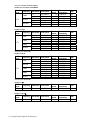
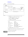
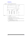
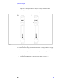
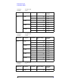
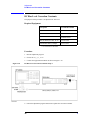
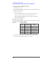
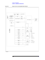
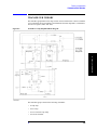
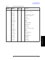
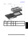
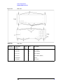
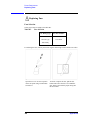
1
Agilent 4294A PRECISION IMPEDANCE ANALYZER Service Manual
Manual Change
Agilent Part No. N/A
May 2009
Change 1
Change the Measurement Uncertainty value of Frequency Accuracy Test (Page 68) to the
following information and appended TAR to this report.
Frequency Accuracy Test
Without Option 1D5
Frequency
10MHz
Test Limit
±200 Hz
Test Result1
Hz
Measurement
Uncertainty
± 0.3 Hz
TAR
Measurement
Uncertainty
± 0.2 Hz
TAR
890
With Option 1D5
Frequency
10MHz
Test Limit
±1.3 Hz
C Copyright 2009 Agilent Technologies
○
Test Result1
Hz
890
Change 2
Change the Measurement Uncertainty value of OSC Level Accuracy Test (Page 69 to 70) to
the following information and appended TAR to this report.
OSC Level Accuracy Test
OSC Level Accuracy (Accessory: Nothing)
OSC
Level
Frequency
Test Limits
1 kHz
± 101 mV
100 kHz
± 101 mV
40 Hz
± 51.0 mV
1 kHz
± 51.0 mV
10 kHz
± 51.0 mV
100 kHz
± 51.0 mV
1 MHz
± 51.3 mV
10 MHz
± 53.5 mV
15 MHz
± 54.8 mV
16 MHz
± 55.0 mV
50 MHz
± 63.5 mV
110 MHz
± 78.5 mV
1 kHz
± 26.0 mV
100 kHz
± 26.0 mV
1 kHz
± 13.5 mV
100 kHz
± 13.5 mV
1 kHz
± 7.4 mV
100 kHz
± 7.4 mV
1 kHz
± 2.6 mV
100 kHz
± 2.6 mV
1.0 V
0.5 V
0.25 V
0.125 V
0.064 V
0.016 V
C Copyright 2009 Agilent Technologies
○
Test Result
mV
mV
mV
mV
mV
mV
mV
mV
mV
mV
mV
mV
mV
mV
mV
mV
mV
mV
mV
mV
Measurement
Uncertainty
TAR
± 0.4 mV
271
± 1.21 mV
84
± 0.06 mV
326
± 0.09 mV
204
± 0.09 mV
289
± 0.42 mV
65
± 5.2 mV
15
± 5.3 mV
20.2
± 5.3 mV
16.1
± 5.3 mV
15.3
± 5.4 mV
16.6
± 5.7 mV
18.2
± 0.06 mV
195.2
± 0.22 mV
80.4
± 0.04 mV
167.8
± 0.12 mV
79.2
± 0.01 mV
269.1
± 0.05 mV
78.9
± 0.004 mV
52.2
± 0.02 mV
46.0
OSC Level Accuracy (with 42942A Terminal Adapter)
OSC
Level
Frequency
Test Limits
0.5 V
1 MHz
10 MHz
15 MHz
16 MHz
50 MHz
110 MHz
± 51.3 mV
± 53.5 mV
± 54.8 mV
± 55.0 mV
± 63.5 mV
± 78.5 mV
Test Result
mV
mV
mV
mV
mV
mV
Measurement
Uncertainty
± 5.2 mV
± 5.3 mV
± 5.3 mV
± 5.3 mV
± 5.4 mV
± 5.7 mV
TAR
19.6
20.0
20.5
20.6
21.0
19.0
Change 3
Change the Measurement Uncertainty value of DC Bias Level Accuracy Test (Page 70 to 71)
to the following information and appended TAR to this report.
DC Bias Monitor Accuracy Test
Bias
Level
0V
25 V
40 V
-25 V
-40 V
0 mA
20 mA
100 mA
-20 mA
-100 mA
Bias
Level
0V
25 V
40 V
-25 V
-40 V
0 mA
20 mA
100 mA
-20 mA
-100 mA
Test Result
Test Limits
± 5.0 mV
± 55.0 mV
± 85.0 mV
± 55.0 mV
± 85.0 mV
± 0.50 mV
± 0.75 mV
± 1.75 mV
± 0.75 mV
± 1.75 mV
mV
mV
mV
mV
mV
mV
mV
mV
mV
mV
Measurement
Uncertainty
± 0.001 mV
± 0.61 mV
± 0.86 mV
± 0.61 mV
± 0.86 mV
± 0.001 mV
± 0.004 mV
± 0.016 mV
± 0.004 mV
± 0.016 mV
mV
mV
mV
mV
mV
mV
mV
mV
mV
mV
Measurement
Uncertainty
± 0.001 mV
± 0.61 mV
± 0.86 mV
± 0.61 mV
± 0.86 mV
± 0.001 mV
± 0.004 mV
± 0.016 mV
± 0.004 mV
± 0.016 mV
Test Result
Test Limits
± 5.0 mV
± 30.3 mV
± 45.6 mV
± 30.3 mV
± 45.6 mV
± 0.20 mV
± 0.60 mV
± 2.20 mV
± 0.60 mV
± 2.20 mV
TAR
4.0
53.4
89.8
40.3
58.7
145.9
107.2
93.1
143.9
72.6
TAR
96.4
49.2
53.0
49.2
53.0
43.8
90.5
115.3
73.4
93.2
Change 4
Change the Measurement Uncertainty value of Measurement Accuracy Test (Page 72 to 80)
to the following information and appended TAR to this report.
Measurement Accuracy Test
C Copyright 2009 Agilent Technologies
○
Accessory: Nothing
Standard: 1pF
OSC
Level
Frequency
1 MHz
0.5 V
3 MHz
Parameter
Test Limits
Cp
D
Cp
D
± 0.0015 pF
± 0.0015
± 0.0057 pF
± 0.0057
Parameter
Test Limits
Cp
D
Cp
D
Cp
D
Cp
D
Cp
D
± 0.41 pF
± 0.041
± 0.0083 pF
± 0.0008
± 0.033 pF
± 0.0033
± 0.101 pF
± 0.0101
± 2.00 pF
± 0.200
Parameter
Test Limits
Cp
D
Cp
D
Cp
D
Cp
D
Cp
D
Cp
D
Cp
D
Cp
D
Cp
D
Cp
D
± 0.47 pF
± 0.0047
± 0.079 pF
± 0.0008
± 0.0076 pF
± 0.0008
± 0.30 pF
± 0.0030
± 1.00 pF
±0.0100
±2.07 pF
± 0.0207
± 0.102 pF
± 0.0010
± 0.087 pF
± 0.0009
± 0.32 pF
± 0.0032
± 1.01 pF
±0.0101
Test
Measurement
Result
Uncertainty
pF ± 0.0005 pF
± 0.0002
pF ± 0.0010 pF
± 0.0008
TAR
5.1
5.2
11.2
18.1
Accessory: Nothing
Standard: 10 pF
OSC
Level
Frequency
1 kHz
1 MHz
0.5 V
3 MHz
10 MHz
0.1V
1 kHz
Test
Measurement
Result
Uncertainty
pF ± 0.0010 pF
± 0.0001
pF ± 0.0025 pF
± 0.0002
pF ± 0.0030 pF
± 0.0005
pF ± 0.015 pF
± 0.003
pF ± 0.0010 pF
± 0.0001
TAR
74.0
34.8
2.8
2.9
11.2
11.2
32.2
30.7
57.6
54.3
Accessory: Nothing
Standard: 100 pF
OSC
Level
Frequency
1 kHz
100 kHz
0.5 V
1 MHz
3 MHz
10 MHz
1 kHz
100 kHz
0.1 V
1 MHz
3 MHz
10 MHz
C Copyright 2009 Agilent Technologies
○
Test
Measurement
Result
Uncertainty
pF ± 0.010 pF
± 0.0001
pF ± 0.025 pF
± 0.0002
pF ± 0.025 pF
± 0.0002
pF ± 0.030 pF
± 0.0005
pF ± 0.15 pF
± 0.003
pF ± 0.010 pF
± 0.0001
pF ± 0.025 pF
± 0.0002
pF ± 0.025 pF
± 0.0002
pF ± 0.030 pF
± 0.0005
pF ± 0.15 pF
± 0.003
TAR
15.4
15.3
2.7
2.7
2.6
2.6
10.2
10.3
22.8
29.2
45.2
44.0
3.4
3.5
3.0
3.0
10.8
10.9
23.1
29.2
Accessory: Nothing
Standard: 1000 pF
OSC
Level
Frequency
1 kHz
0.5 V
10 kHz
100 kHz
0.1 V
1 kHz
Parameter
Test Limits
Cp
D
Cp
D
Cp
D
Cp
D
± 1.15 pF
± 0.0012
± 0.79 pF
± 0.0008
± 0.76 pF
± 0.0008
± 2.8 pF
± 0.0028
Parameter
Test Limits
Cp
D
Cp
D
Cp
D
Cp
D
± 0.033 nF
± 0.0033
± 0.0079 nF
± 0.0008
± 0.0076 nF
± 0.0008
± 0.0102 nF
± 0.0010
Parameter
Test Limits
Cp
D
Cp
D
Cp
D
Cp
D
± 0.30 nF
± 0.0030
± 0.076 nF
± 0.0008
± 0.077 nF
± 0.0008
± 0.085 nF
± 0.0008
Parameter
Test Limits
Cp
D
Cp
D
Cp
D
± 0.0030 μF
± 0.0030
±0.00077μF
± 0.0008
±0.00085μF
± 0.0008
Test
Measurement
Result
Uncertainty
pF ± 0.10 pF
± 0.0001
pF ± 0.10 pF
± 0.0001
pF ± 0.10 pF
± 0.0001
pF ± 0.10 pF
± 0.0001
TAR
3.8
3.9
2.7
2.7
2.5
2.5
9.2
9.0
Accessory: Nothing
Standard: 0.01 μF
OSC
Level
Frequency
120 Hz
0.5 V
1 kHz
10 kHz
0.1 V
1 kHz
Test
Measurement
Result
Uncertainty
nF ± 0.0025 nF
± 0.0001
nF ± 0.001 nF
± 0.0001
nF ± 0.0025 nF
± 0.0002
nF ± 0.001 nF
± 0.0001
TAR
12.4
12.5
3.0
3.0
2.9
2.8
3.8
3.8
Accessory: Nothing
Standard: 0.1 μF
OSC
Level
Frequency
120 Hz
0.5 V
1 kHz
10 kHz
0.1 V
1 kHz
Test
Measurement
Result
Uncertainty
nF ± 0.0025 nF
± 0.0001
nF ± 0.01 nF
± 0.0001
nF ± 0.025 nF
± 0.0002
nF ± 0.01 nF
± 0.0001
TAR
11.5
11.3
2.8
2.9
2.9
2.8
3.1
3.2
Accessory: Nothing
Standard: 1 μF
OSC
Level
Frequency
120 Hz
0.5 V
1 kHz
0.1 V
1 kHz
C Copyright 2009 Agilent Technologies
○
Test
Measurement
Result
Uncertainty
μF ± 0.0004 μF
± 0.00015
μF ± 0.0001 μF
± 0.0001
μF ± 0.0001 μF
± 0.0001
TAR
11.3
11.4
2.9
2.9
3.1
3.2
Accessory: Nothing
Standard: 10 Ω
OSC
Level
0.5 V
0.1 V
Frequency
Parameter
Test Limits
1 kHz
1 kHz
R
R
± 0.0100 Ω
± 0.0114 Ω
Frequency
Parameter
Test Limits
1 kHz
1 kHz
R
R
± 0.0033 Ω
± 0.0040 Ω
Frequency
Parameter
Test Limits
1 kHz
1 kHz
R
R
± 2.6 mΩ
± 3.2 mΩ
Test
Result
Ω
Ω
Measurement
Uncertainty
± 0.003 Ω
± 0.003 Ω
Test
Result
Ω
Ω
Measurement
Uncertainty
± 0.001 Ω
± 0.001 Ω
Test
Result
mΩ
mΩ
Measurement
Uncertainty
± 0.1 mΩ
± 0.1 mΩ
Test
Result
mΩ
mΩ
Measurement
Uncertainty
± 0.01 mΩ
± 0.01 mΩ
Test
Result
Ω
mrad
Ω
mrad
Ω
mrad
Ω
mrad
Measurement
Uncertainty
± 0.090 Ω
± 1.8 mrad
± 0.090 Ω
± 1.8 mrad
± 0.090 Ω
± 1.8 mrad
± 0.010 Ω
± 2.0 mrad
Test
Result
Ω
mrad
Ω
mrad
Ω
mrad
Measurement
Uncertainty
± 44 Ω
± 2.0 mrad
± 4.4 Ω
± 2.0 mrad
± 0.43 Ω
± 2.0 mrad
TAR
4.9
6.3
Accessory: Nothing
Standard: 1 Ω
OSC
Level
0.5 V
0.1 V
TAR
13.6
14.7
Accessory: Nothing
Standard: 100 mΩ
OSC
Level
0.5 V
0.1 V
TAR
13.0
31.0
Accessory: Nothing
Standard: 10 mΩ
OSC
Level
0.5 V
0.1 V
Frequency
Parameter Test Limits
1 kHz
1 kHz
R
R
± 2.5 mΩ
± 3.1 mΩ
TAR
10.2
38.9
Accessory: 42942A Terminal Adapter
Standard: 50 Ω
OSC
Level
Frequency
Parameter Test Limits
⏐Z⏐
θ
⏐Z⏐
1 MHz
θ
0.5 V
⏐Z⏐
10 MHz
θ
⏐Z⏐
100 MHz
θ
Accessory: 42942A Terminal Adapter
1 kHz
± 0.31 Ω
± 6.1 mrad
± 0.31 Ω
± 6.1 mrad
± 0.31 Ω
± 6.2 mrad
± 0.54 Ω
± 10.9 mrad
TAR
2.8
3.4
2.8
3.4
2.8
3.4
4.0
5.5
Standard: 10 cm Airline with OPEN
OSC
Level
Frequency
1 MHz
0.5 V
10 MHz
100 MHz
Parameter Test Limits
⏐Z⏐
θ
⏐Z⏐
θ
⏐Z⏐
θ
C Copyright 2009 Agilent Technologies
○
± 155 Ω
± 7.1 mrad
± 15.7 Ω
± 7.2 mrad
± 2.32 Ω
± 10.8 mrad
TAR
4.1
3.6
3.7
3.6
7.3
5.4
Accessory: 42942A Terminal Adapter
Standard: 10 cm Airline with SHORT
OSC
Level
Frequency
1 MHz
0.5 V
10 MHz
100 MHz
Parameter Test Limits
⏐Z⏐
θ
⏐Z⏐
θ
⏐Z⏐
θ
± 0.0062 Ω
± 54.4 mrad
± 0.0165 Ω
± 15.3 mrad
± 0.157 Ω
± 14.7 mrad
Test
Result
Ω
mrad
Ω
mrad
Ω
mrad
Measurement
Uncertainty
± 0.0017 Ω
± 2.0 mrad
± 0.0043 Ω
± 4.0 mrad
± 0.027 Ω
± 2.5 mrad
TAR
3.5
27.2
2.0
3.8
1.5
5.9
Accessory: 1m Test Leads
Standard: 10 pF
OSC
Level
Frequency
1 kHz
1 MHz
0.5 V
3 MHz
10 MHz
Parameter Test Limits
Cp
D
Cp
D
Cp
D
Cp
D
± 0.41 pF
± 0.041
± 0.013 pF
± 0.0013
± 0.041 pF
± 0.0041
± 0.124 pF
± 0.0124
Test
Measurement
Result
Uncertainty
pF ± 0.0010 pF
± 0.0001
pF ± 0.0025 pF
± 0.0002
pF ± 0.0030 pF
± 0.0005
pF ± 0.0010 pF
± 0.003
TAR
61.9
53.1
4.5
4.5
14.2
14.3
39.3
32.7
Accessory: 1m Test Leads
Standard: 100 pF
OSC
Level
Frequency
1 kHz
100 kHz
0.5 V
1 MHz
3 MHz
10 MHz
Parameter Test Limits
Cp
D
Cp
D
Cp
D
Cp
D
Cp
D
± 0.49 pF
± 0.0049
± 0.102 pF
± 0.0010
± 0.128 pF
± 0.0013
± 0.38 pF
± 0.0038
± 1.22 pF
± 0.0122
Test
Measurement
Result
Uncertainty
pF ± 0.010 pF
± 0.0001
pF ± 0.025 pF
± 0.0002
pF ± 0.025 pF
± 0.0002
pF ± 0.0030 pF
± 0.0005
pF ± 0.15 pF
± 0.003
TAR
16.5
15.5
3.5
3.5
4.0
4.0
12.9
13.2
27.2
31.4
Accessory: 1m Test Leads
Standard: 1 Ω
OSC
Level
0.5 V
Frequency
Parameter Test Limits
1 kHz
R
± 0.0055 Ω
Test
Measurement
Result
Uncertainty
Ω ± 0.001Ω
TAR
21.7
Accessory: 1m Test Leads
Standard: 100 mΩ
OSC
Level
0.5 V
Frequency
Parameter Test Limits
1 kHz
R
C Copyright 2009 Agilent Technologies
○
± 4.6 mΩ
Test
Measurement
Result
Uncertainty
mΩ ± 0.1 mΩ
TAR
19.2
Accessory: 2m Test Leads
Standard: 10 pF
OSC
Level
Frequency
1 kHz
1 MHz
0.5 V
3 MHz
10 MHz
Parameter Test Limits
Cp
D
Cp
D
Cp
D
Cp
D
± 0.41 pF
± 0.041
± 0.015 pF
± 0.0015
± 0.045 pF
± 0.0045
± 0.134 pF
± 0.0134
Test
Measurement
Result
Uncertainty
pF ± 0.0010 pF
± 0.0001
pF ± 0.0025 pF
± 0.0002
pF ± 0.0030 pF
± 0.0005
pF ± 0.015 pF
± 0.003
TAR
46.6
81.6
5.0
5.1
13.0
15.5
29.5
10.6
Accessory: 2m Test Leads
Standard: 100 pF
OSC
Level
Frequency
1 kHz
100 kHz
0.5 V
1 MHz
3 MHz
10 MHz
Parameter Test Limits
Cp
D
Cp
D
Cp
D
Cp
D
Cp
D
± 0.49 pF
± 0.0049
± 0.104 pF
± 0.0010
± 0.128 pF
± 0.0013
± 0.42 pF
± 0.0042
± 1.33 pF
± 0.0133
Test
Measurement
Result
Uncertainty
pF ± 0.010 pF
± 0.0001
pF ± 0.025 pF
± 0.0002
pF ± 0.025 pF
± 0.0002
pF ± 0.030 pF
± 0.0005
pF ± 0.15 pF
± 0.003
TAR
14.1
12.2
3.4
3.6
4.3
4.4
10.0
13.2
6.0
31.5
Accessory: 2m Test Leads
Standard: 1 Ω
OSC
Level
0.5 V
Frequency
Parameter Test Limits
1 kHz
R
± 0.0055 Ω
Test
Measurement
Result
Uncertainty
Ω ± 0.001 Ω
TAR
16.4
Accessory: 2m Test Leads
Standard: 100 mΩ
OSC
Level
Frequency
Parameter Test Limits
0.5 V
1 kHz
R
C Copyright 2009 Agilent Technologies
○
± 4.6 mΩ
Test
Result
Measurement
Uncertainty
mΩ ± 0.1 mΩ
TAR
22.4
Agilent 4294A Precision Impedance Analyzer
Service Manual
Third Edition
Manufacturing No. 04294-90110
January 2007
Notices
The information contained in this document is subject to change without notice.
This document contains proprietary information that is protected by copyright. All rights
are reserved. No part of this document may be photocopied, reproduced, or translated to
another language without the prior written consent of Agilent Technologies.
Microsoft®,MS-DOS®,Windows®,Visual C++®,Visual Basic®,VBA® and Excel® are
registered
UNIX is a registered trademark in U.S. and other countries, licensed
exclusively through X/Open Company Limited.
Portions ©Copyright 1996, Microsoft Corporation. All rights reserved.
© Copyright 1999, 2000, 2007 Agilent Technologies
Manual Printing History
The manual’s printing date and part number indicate its current edition. The printing date
changes when a new edition is printed. (Minor corrections and updates that are
incorporated at reprint do not cause the date to change.) The manual part number changes
when extensive technical changes are incorporated.
October 1999
First Edition
June 2000
Second Edition
January 2007
Third Edition
2
Safety Summary
The following general safety precautions must be observed during all phases of operation,
service, and repair of this instrument. Failure to comply with these precautions or with
specific WARNINGS elsewhere in this manual may impair the protection provided by the
equipment. In addition it violates safety standards of design, manufacture, and intended use
of the instrument.
The Agilent Technologies Company assumes no liability for the customer’s failure to
comply with these requirements.
NOTE
4294A comply with INSTALLATION CATEGORY II and POLLUTION DEGREE 2 in
IEC61010-1. 4294A are INDOOR USE product.
NOTE
LEDs in 4294A are Class 1 in accordance with IEC60825-1.
CLASS 1 LED PRODUCT
•
Ground The Instrument
To avoid electric shock hazard, the instrument chassis and cabinet must be connected to
a safety earth ground by the supplied power cable with earth blade.
•
DO NOT Operate In An Explosive Atmosphere
Do not operate the instrument in the presence of flammable gasses or fumes. Operation
of any electrical instrument in such an environment constitutes a definite safety hazard.
•
Keep Away From Live Circuits
Operating personnel must not remove instrument covers. Component replacement and
internal adjustments must be made by qualified maintenance personnel. Do not replace
components with the power cable connected. Under certain conditions, dangerous
voltages may exist even with the power cable removed. To avoid injuries, always
disconnect power and discharge circuits before touching them.
•
DO NOT Service Or Adjust Alone
Do not attempt internal service or adjustment unless another person, capable of
rendering first aid and resuscitation, is present.
•
DO NOT Substitute Parts Or Modify Instrument
Because of the danger of introducing additional hazards, do not install substitute parts
or perform unauthorized modifications to the instrument. Return the instrument to a
Agilent Technologies Sales and Service Office for service and repair to ensure that
safety features are maintained.
•
Dangerous Procedure Warnings
Warnings, such as the example below, precede potentially dangerous procedures
throughout this manual. Instructions contained in the warnings must be followed.
WARNING
Dangerous voltages, capable of causing death, are presenting this instrument. Use
extreme caution when handling, testing, and adjusting this instrument.
3
Safety Symbol
General definitions of safety symbols used on the instrument or in manuals are listed
below.
Instruction Manual symbol: the product is marked with this symbol when it is necessary for
the user to refer to the instrument manual.
Alternating current.
Direct current.
On (Supply).
Off (Supply).
In position of push-button switch.
Out position of push-button switch.
Frame (or chassis) terminal. A connection to the frame (chassis) of the equipment which
normally include all exposed metal structure.
WARNING
This warning sign denotes a hazard. It calls attention to a procedure, practice,
condition or the like, which, if not correctly performed or adhered to, could result in
injury or death to personnel.
CAUTION
This Caution sign denotes a hazard. It calls attention to a procedure, practice, condition or
the like, which, if not correctly performed or adhered to, could result in damage to or
destruction of part or all of the product.
NOTE
Note denotes important information. It calls attention to a procedure, practice, condition or
the like, which is essential to highlight.
Certification
Agilent Technologies Company certifies that this product met its published specifications
at the time of shipment from the factory. Agilent Technologies further certifies that its
calibration measurements are traceable to the United States National Institute of Standards
and Technology, to the extent allowed by the Institution’s calibration facility, or to the
calibration facilities of other International Standards Organization members.
4
Warranty
This Agilent Technologies instrument product is warranted against defects in material and
workmanship for a period corresponding to the individual warranty periods of its
component products. Instruments are warranted for a period of one year. Fixtures and
adapters are warranted for a period of 90 days. During the warranty period, Agilent
Technologies Company will, at its option, either repair or replace products that prove to be
defective.
For warranty service or repair, this product must be returned to a service facility designated
by Agilent Technologies. Buyer shall prepay shipping charges to Agilent Technologies and
Agilent Technologies shall pay shipping charges to return the product to Buyer. However,
Buyer shall pay all shipping charges, duties, and taxes for products returned to Agilent
Technologies from another country.
Agilent Technologies warrants that its software and firmware designated by Agilent
Technologies for use with an instrument will execute its programming instruction when
property installed on that instrument. Agilent Technologies does not warrant that the
operation of the instrument, or software, or firmware will be uninterrupted or error free.
Limitation of Warranty
The foregoing warranty shall not apply to defects resulting from improper or inadequate
maintenance by Buyer, Buyer-supplied software or interfacing, unauthorized modification
or misuse, operation outside the environmental specifications for the product, or improper
site preparation or maintenance.
IMPORTANT
No other warranty is expressed or implied. Agilent Technologies specifically disclaims the
implied warranties of merchantability and fitness for a particular purpose.
Exclusive Remedies
The remedies provided herein are buyer’s sole and exclusive remedies. Agilent
Technologies shall not be liable for any direct, indirect, special, incidental, or
consequential damages, whether based on contract, tort, or any other legal theory.
Assistance
Product maintenance agreements and other customer assistance agreements are available
for Agilent Technologies products.
5
For any assistance, contact your nearest Agilent Technologies Sales and Service Office.
Addresses are provided at the back of this manual.
Typeface Conventions
Bold
Boldface type is used when a term is defined. For
example: icons are symbols.
Italic
Italic type is used for emphasis and for titles of
manuals and other publications.
[Hardkey]
Indicates a hardkey labeled “Hardkey.”
Softkey
Indicates a softkey labeled “Softkey.”
[Hardkey] - Softkey1 - Softkey2
Indicates keystrokes [Hardkey] - Softkey1 Softkey2.
4294A Documentation Map
The following manuals are available for the 4294A.
•
Operation Manual (Agilent P/N: 04294-900x0)
Most of basic information necessary for using 4294A is described in this manual. It
includes the way of installation, preparation, measurement operation including
calibration, performances (specifications), key definitions, and error messages. For
GPIB programming, see the Programming Manual together with “HP Instrument
BASIC User's Handbook”.
•
Programming Manual (Agilent P/N: 04294-900x1)
The Programming Manual shows how to write and use BASIC program to control the
4294A and describes how HP Instrument BASIC works with the analyzer.
•
HP Instrument BASIC User's Handbook (Agilent P/N: E2083-90005)
The HP Instrument BASIC User’s Handbook introduces you to the HP Instrument
BASIC programming language, provide some helpful hints on getting the most use
from it, and provide a general programming reference. It is divided into three books,
HP Instrument BASIC Programming Techniques, HP Instrument BASIC Interface
Techniques, and HP Instrument BASIC Language Reference.
•
Service Manual (Agilent P/N: 04294-901x0, Option 0BW only)
This manual describes how to adjust and repair the 4294A, and how to carry out
performance tests. This manual will be attached if you take the Option 0BW.
NOTE
The number position shown by “x” in the part numbers above indicates the edition number.
6
Contents
1. General Information
Organization of Service Manual . . . . . . . . . . . . . . . . . . . . . . . . . . . . . . . . . . . . . . . . . . . . . . . . . . . . . . . . . . 14
Instruments Covered by This Manual. . . . . . . . . . . . . . . . . . . . . . . . . . . . . . . . . . . . . . . . . . . . . . . . . . . . . . 15
Require Equipment . . . . . . . . . . . . . . . . . . . . . . . . . . . . . . . . . . . . . . . . . . . . . . . . . . . . . . . . . . . . . . . . . . . . 16
2. Performance Test
Performance Test . . . . . . . . . . . . . . . . . . . . . . . . . . . . . . . . . . . . . . . . . . . . . . . . . . . . . . . . . . . . . . . . . . . . . 20
Introduction . . . . . . . . . . . . . . . . . . . . . . . . . . . . . . . . . . . . . . . . . . . . . . . . . . . . . . . . . . . . . . . . . . . . . . . . 20
Test Equipment . . . . . . . . . . . . . . . . . . . . . . . . . . . . . . . . . . . . . . . . . . . . . . . . . . . . . . . . . . . . . . . . . . . . . 20
Frequency Accuracy Test . . . . . . . . . . . . . . . . . . . . . . . . . . . . . . . . . . . . . . . . . . . . . . . . . . . . . . . . . . . . . 21
OSC Level Accuracy Test . . . . . . . . . . . . . . . . . . . . . . . . . . . . . . . . . . . . . . . . . . . . . . . . . . . . . . . . . . . . . 23
DC Bias Monitor Accuracy Test . . . . . . . . . . . . . . . . . . . . . . . . . . . . . . . . . . . . . . . . . . . . . . . . . . . . . . . . 31
DC Bias Level Accuracy Test . . . . . . . . . . . . . . . . . . . . . . . . . . . . . . . . . . . . . . . . . . . . . . . . . . . . . . . . . . 35
Measurement Accuracy Test . . . . . . . . . . . . . . . . . . . . . . . . . . . . . . . . . . . . . . . . . . . . . . . . . . . . . . . . . . . 38
Calculation Sheet . . . . . . . . . . . . . . . . . . . . . . . . . . . . . . . . . . . . . . . . . . . . . . . . . . . . . . . . . . . . . . . . . . . . . 52
OSC Level Accuracy Test . . . . . . . . . . . . . . . . . . . . . . . . . . . . . . . . . . . . . . . . . . . . . . . . . . . . . . . . . . . . . 52
DC Bias Monitor Accuracy Test . . . . . . . . . . . . . . . . . . . . . . . . . . . . . . . . . . . . . . . . . . . . . . . . . . . . . . . . 54
DC Bias Level Accuracy Test . . . . . . . . . . . . . . . . . . . . . . . . . . . . . . . . . . . . . . . . . . . . . . . . . . . . . . . . . . 55
Measurement Accuracy Test . . . . . . . . . . . . . . . . . . . . . . . . . . . . . . . . . . . . . . . . . . . . . . . . . . . . . . . . . . . 56
Performance Test Record . . . . . . . . . . . . . . . . . . . . . . . . . . . . . . . . . . . . . . . . . . . . . . . . . . . . . . . . . . . . . . . 68
Frequency Accuracy Test . . . . . . . . . . . . . . . . . . . . . . . . . . . . . . . . . . . . . . . . . . . . . . . . . . . . . . . . . . . . . 68
OSC Level Accuracy Test . . . . . . . . . . . . . . . . . . . . . . . . . . . . . . . . . . . . . . . . . . . . . . . . . . . . . . . . . . . . . 69
DC Bias Monitor Accuracy Test . . . . . . . . . . . . . . . . . . . . . . . . . . . . . . . . . . . . . . . . . . . . . . . . . . . . . . . . 70
DC Bias Level Accuracy Test . . . . . . . . . . . . . . . . . . . . . . . . . . . . . . . . . . . . . . . . . . . . . . . . . . . . . . . . . . 71
Measurement Accuracy Test . . . . . . . . . . . . . . . . . . . . . . . . . . . . . . . . . . . . . . . . . . . . . . . . . . . . . . . . . . . 72
3. Adjustment
Safety Considerations . . . . . . . . . . . . . . . . . . . . . . . . . . . . . . . . . . . . . . . . . . . . . . . . . . . . . . . . . . . . . . . . . . 82
Required Controller . . . . . . . . . . . . . . . . . . . . . . . . . . . . . . . . . . . . . . . . . . . . . . . . . . . . . . . . . . . . . . . . . . . 82
Required Equipment . . . . . . . . . . . . . . . . . . . . . . . . . . . . . . . . . . . . . . . . . . . . . . . . . . . . . . . . . . . . . . . . . . . 82
Warm-up for Adjustment . . . . . . . . . . . . . . . . . . . . . . . . . . . . . . . . . . . . . . . . . . . . . . . . . . . . . . . . . . . . . . . 82
Order of Adjustment . . . . . . . . . . . . . . . . . . . . . . . . . . . . . . . . . . . . . . . . . . . . . . . . . . . . . . . . . . . . . . . . . . . 83
Preparation for using the Adjustment Program . . . . . . . . . . . . . . . . . . . . . . . . . . . . . . . . . . . . . . . . . . . . . . 84
Installing an GPIB Card (82340, 82341 or 82350) . . . . . . . . . . . . . . . . . . . . . . . . . . . . . . . . . . . . . . . . . . 84
Installing HP VEE for Personal Computer . . . . . . . . . . . . . . . . . . . . . . . . . . . . . . . . . . . . . . . . . . . . . . . . 84
Installing Adjustment Program into Your PC (preliminary) . . . . . . . . . . . . . . . . . . . . . . . . . . . . . . . . . . . 84
Equipment Setup . . . . . . . . . . . . . . . . . . . . . . . . . . . . . . . . . . . . . . . . . . . . . . . . . . . . . . . . . . . . . . . . . . . . 84
Running the Adjustment Program . . . . . . . . . . . . . . . . . . . . . . . . . . . . . . . . . . . . . . . . . . . . . . . . . . . . . . . . 86
Frequency Accuracy Correction Constants . . . . . . . . . . . . . . . . . . . . . . . . . . . . . . . . . . . . . . . . . . . . . . . . . 87
Required Equipment . . . . . . . . . . . . . . . . . . . . . . . . . . . . . . . . . . . . . . . . . . . . . . . . . . . . . . . . . . . . . . . . . 87
Procedure. . . . . . . . . . . . . . . . . . . . . . . . . . . . . . . . . . . . . . . . . . . . . . . . . . . . . . . . . . . . . . . . . . . . . . . . . . 87
Image Rejection Correction Constants . . . . . . . . . . . . . . . . . . . . . . . . . . . . . . . . . . . . . . . . . . . . . . . . . . . . . 88
Required Equipment . . . . . . . . . . . . . . . . . . . . . . . . . . . . . . . . . . . . . . . . . . . . . . . . . . . . . . . . . . . . . . . . . 88
Procedure. . . . . . . . . . . . . . . . . . . . . . . . . . . . . . . . . . . . . . . . . . . . . . . . . . . . . . . . . . . . . . . . . . . . . . . . . . 88
LPOT-Mixer Offset Correction Constants . . . . . . . . . . . . . . . . . . . . . . . . . . . . . . . . . . . . . . . . . . . . . . . . . . 89
Required Equipment . . . . . . . . . . . . . . . . . . . . . . . . . . . . . . . . . . . . . . . . . . . . . . . . . . . . . . . . . . . . . . . . . 89
Procedure. . . . . . . . . . . . . . . . . . . . . . . . . . . . . . . . . . . . . . . . . . . . . . . . . . . . . . . . . . . . . . . . . . . . . . . . . . 89
Null Detector Offset Correction Constants. . . . . . . . . . . . . . . . . . . . . . . . . . . . . . . . . . . . . . . . . . . . . . . . . . 90
7
Contents
Required Equipment . . . . . . . . . . . . . . . . . . . . . . . . . . . . . . . . . . . . . . . . . . . . . . . . . . . . . . . . . . . . . . . . . 90
Procedure . . . . . . . . . . . . . . . . . . . . . . . . . . . . . . . . . . . . . . . . . . . . . . . . . . . . . . . . . . . . . . . . . . . . . . . . . 90
Null Loop Phase Correction Constants . . . . . . . . . . . . . . . . . . . . . . . . . . . . . . . . . . . . . . . . . . . . . . . . . . . . 91
Required Equipment . . . . . . . . . . . . . . . . . . . . . . . . . . . . . . . . . . . . . . . . . . . . . . . . . . . . . . . . . . . . . . . . . 91
Procedure . . . . . . . . . . . . . . . . . . . . . . . . . . . . . . . . . . . . . . . . . . . . . . . . . . . . . . . . . . . . . . . . . . . . . . . . . 91
HPOT-Amplifier Offset Correction Constants . . . . . . . . . . . . . . . . . . . . . . . . . . . . . . . . . . . . . . . . . . . . . . . 92
Required Equipment . . . . . . . . . . . . . . . . . . . . . . . . . . . . . . . . . . . . . . . . . . . . . . . . . . . . . . . . . . . . . . . . . 92
Procedure . . . . . . . . . . . . . . . . . . . . . . . . . . . . . . . . . . . . . . . . . . . . . . . . . . . . . . . . . . . . . . . . . . . . . . . . . 92
Relative Impedance Correction Constants . . . . . . . . . . . . . . . . . . . . . . . . . . . . . . . . . . . . . . . . . . . . . . . . . . 93
Required Equipment . . . . . . . . . . . . . . . . . . . . . . . . . . . . . . . . . . . . . . . . . . . . . . . . . . . . . . . . . . . . . . . . . 93
Procedure . . . . . . . . . . . . . . . . . . . . . . . . . . . . . . . . . . . . . . . . . . . . . . . . . . . . . . . . . . . . . . . . . . . . . . . . . 93
DC Bias Monitor Correction Constants . . . . . . . . . . . . . . . . . . . . . . . . . . . . . . . . . . . . . . . . . . . . . . . . . . . . 94
Required Equipment . . . . . . . . . . . . . . . . . . . . . . . . . . . . . . . . . . . . . . . . . . . . . . . . . . . . . . . . . . . . . . . . . 94
Procedure . . . . . . . . . . . . . . . . . . . . . . . . . . . . . . . . . . . . . . . . . . . . . . . . . . . . . . . . . . . . . . . . . . . . . . . . . 94
DC Bias Level Correction Constants . . . . . . . . . . . . . . . . . . . . . . . . . . . . . . . . . . . . . . . . . . . . . . . . . . . . . . 96
Required Equipment . . . . . . . . . . . . . . . . . . . . . . . . . . . . . . . . . . . . . . . . . . . . . . . . . . . . . . . . . . . . . . . . . 96
Procedure . . . . . . . . . . . . . . . . . . . . . . . . . . . . . . . . . . . . . . . . . . . . . . . . . . . . . . . . . . . . . . . . . . . . . . . . . 96
OSC Level Monitor Correction Constants . . . . . . . . . . . . . . . . . . . . . . . . . . . . . . . . . . . . . . . . . . . . . . . . . . 97
Required Equipment . . . . . . . . . . . . . . . . . . . . . . . . . . . . . . . . . . . . . . . . . . . . . . . . . . . . . . . . . . . . . . . . . 97
Procedure . . . . . . . . . . . . . . . . . . . . . . . . . . . . . . . . . . . . . . . . . . . . . . . . . . . . . . . . . . . . . . . . . . . . . . . . . 97
OSC Level Correction Constants . . . . . . . . . . . . . . . . . . . . . . . . . . . . . . . . . . . . . . . . . . . . . . . . . . . . . . . . . 99
Required Equipment . . . . . . . . . . . . . . . . . . . . . . . . . . . . . . . . . . . . . . . . . . . . . . . . . . . . . . . . . . . . . . . . . 99
Procedure . . . . . . . . . . . . . . . . . . . . . . . . . . . . . . . . . . . . . . . . . . . . . . . . . . . . . . . . . . . . . . . . . . . . . . . . . 99
Impedance Measurement Correction Constants. . . . . . . . . . . . . . . . . . . . . . . . . . . . . . . . . . . . . . . . . . . . . 100
Required Equipment . . . . . . . . . . . . . . . . . . . . . . . . . . . . . . . . . . . . . . . . . . . . . . . . . . . . . . . . . . . . . . . . 100
Procedure . . . . . . . . . . . . . . . . . . . . . . . . . . . . . . . . . . . . . . . . . . . . . . . . . . . . . . . . . . . . . . . . . . . . . . . . 100
Frequency Reference Adjustment (Opt.1D5 only). . . . . . . . . . . . . . . . . . . . . . . . . . . . . . . . . . . . . . . . . . . 103
Required Equipment . . . . . . . . . . . . . . . . . . . . . . . . . . . . . . . . . . . . . . . . . . . . . . . . . . . . . . . . . . . . . . . . 103
Procedure . . . . . . . . . . . . . . . . . . . . . . . . . . . . . . . . . . . . . . . . . . . . . . . . . . . . . . . . . . . . . . . . . . . . . . . . 103
4. Troubleshooting
TROUBLESHOOTING SUMMARY . . . . . . . . . . . . . . . . . . . . . . . . . . . . . . . . . . . . . . . . . . . . . . . . . . . .
START HERE. . . . . . . . . . . . . . . . . . . . . . . . . . . . . . . . . . . . . . . . . . . . . . . . . . . . . . . . . . . . . . . . . . . . . . .
INSPECT THE POWER ON SEQUENCE . . . . . . . . . . . . . . . . . . . . . . . . . . . . . . . . . . . . . . . . . . . . . . . .
Check the Fan . . . . . . . . . . . . . . . . . . . . . . . . . . . . . . . . . . . . . . . . . . . . . . . . . . . . . . . . . . . . . . . . . . . . .
Check the Front Panel LEDs and Displays. . . . . . . . . . . . . . . . . . . . . . . . . . . . . . . . . . . . . . . . . . . . . . .
Check Error Message . . . . . . . . . . . . . . . . . . . . . . . . . . . . . . . . . . . . . . . . . . . . . . . . . . . . . . . . . . . . . . .
INSPECT THE REAR PANEL FEATURE . . . . . . . . . . . . . . . . . . . . . . . . . . . . . . . . . . . . . . . . . . . . . . . .
Check the GPIB Interface . . . . . . . . . . . . . . . . . . . . . . . . . . . . . . . . . . . . . . . . . . . . . . . . . . . . . . . . . . . .
Check the Parallel Interface . . . . . . . . . . . . . . . . . . . . . . . . . . . . . . . . . . . . . . . . . . . . . . . . . . . . . . . . . .
Check the mini DIN Keyboard Connector . . . . . . . . . . . . . . . . . . . . . . . . . . . . . . . . . . . . . . . . . . . . . . .
Internal Tests Failure Troubleshooting. . . . . . . . . . . . . . . . . . . . . . . . . . . . . . . . . . . . . . . . . . . . . . . . . . . .
Check the Power-On Selftest . . . . . . . . . . . . . . . . . . . . . . . . . . . . . . . . . . . . . . . . . . . . . . . . . . . . . . . . .
Execute All Internal Tests. . . . . . . . . . . . . . . . . . . . . . . . . . . . . . . . . . . . . . . . . . . . . . . . . . . . . . . . . . . .
Execute the Individual Test. . . . . . . . . . . . . . . . . . . . . . . . . . . . . . . . . . . . . . . . . . . . . . . . . . . . . . . . . . .
External Tests Failure Troubleshooting . . . . . . . . . . . . . . . . . . . . . . . . . . . . . . . . . . . . . . . . . . . . . . . . . . .
Performance Tests Failure Troubleshooting. . . . . . . . . . . . . . . . . . . . . . . . . . . . . . . . . . . . . . . . . . . . . . . .
Perform Adjustments and Correction Constants . . . . . . . . . . . . . . . . . . . . . . . . . . . . . . . . . . . . . . . . . .
8
106
108
109
109
109
109
110
110
110
110
111
111
111
111
113
115
115
Contents
5. Power Supply Troubleshooting
INTRODUCTION . . . . . . . . . . . . . . . . . . . . . . . . . . . . . . . . . . . . . . . . . . . . . . . . . . . . . . . . . . . . . . . . . . . 118
START HERE . . . . . . . . . . . . . . . . . . . . . . . . . . . . . . . . . . . . . . . . . . . . . . . . . . . . . . . . . . . . . . . . . . . . . . . 120
1. Check the Fan . . . . . . . . . . . . . . . . . . . . . . . . . . . . . . . . . . . . . . . . . . . . . . . . . . . . . . . . . . . . . . . . . . . 120
2.Check the A50 SHUTDOWN LED . . . . . . . . . . . . . . . . . . . . . . . . . . . . . . . . . . . . . . . . . . . . . . . . . . . 120
A50 Shutdown LED . . . . . . . . . . . . . . . . . . . . . . . . . . . . . . . . . . . . . . . . . . . . . . . . . . . . . . . . . . . . . . . . 121
3.Check the A50 Five LEDs . . . . . . . . . . . . . . . . . . . . . . . . . . . . . . . . . . . . . . . . . . . . . . . . . . . . . . . . . . 121
4. Check the A1 +5 VD LED . . . . . . . . . . . . . . . . . . . . . . . . . . . . . . . . . . . . . . . . . . . . . . . . . . . . . . . . . 121
5. Check the A9 Two LEDs . . . . . . . . . . . . . . . . . . . . . . . . . . . . . . . . . . . . . . . . . . . . . . . . . . . . . . . . . . 122
FIND OUT WHY THE FAN IS NOT ROTATING . . . . . . . . . . . . . . . . . . . . . . . . . . . . . . . . . . . . . . . . . . 125
1. Check the Line Voltage, Selector Switch Setting, and Fuse . . . . . . . . . . . . . . . . . . . . . . . . . . . . . . . . 125
2. Check the A40 Pre-Regulator . . . . . . . . . . . . . . . . . . . . . . . . . . . . . . . . . . . . . . . . . . . . . . . . . . . . . . . 125
3. Check the A50 SHUTDOWN LED . . . . . . . . . . . . . . . . . . . . . . . . . . . . . . . . . . . . . . . . . . . . . . . . . . 126
FIND OUT WHY THE A50 SHUTDOWN LED IS OFF . . . . . . . . . . . . . . . . . . . . . . . . . . . . . . . . . . . . . 127
1. Disconnect the Cable from the A50P3 . . . . . . . . . . . . . . . . . . . . . . . . . . . . . . . . . . . . . . . . . . . . . . . . 127
2. Remove A50 . . . . . . . . . . . . . . . . . . . . . . . . . . . . . . . . . . . . . . . . . . . . . . . . . . . . . . . . . . . . . . . . . . . . 127
3. Remove Assemblies . . . . . . . . . . . . . . . . . . . . . . . . . . . . . . . . . . . . . . . . . . . . . . . . . . . . . . . . . . . . . . 127
FIND OUT WHY THE A1 +5 VD LED IS NOT ON STEADILY . . . . . . . . . . . . . . . . . . . . . . . . . . . . . . 128
1. Check the A50 DC-DC Converter . . . . . . . . . . . . . . . . . . . . . . . . . . . . . . . . . . . . . . . . . . . . . . . . . . . 128
2. Measure the A1 +5VD Voltage . . . . . . . . . . . . . . . . . . . . . . . . . . . . . . . . . . . . . . . . . . . . . . . . . . . . . . 128
3. Disconnect Cables on the A1 CPU . . . . . . . . . . . . . . . . . . . . . . . . . . . . . . . . . . . . . . . . . . . . . . . . . . . 128
3. Remove Assemblies . . . . . . . . . . . . . . . . . . . . . . . . . . . . . . . . . . . . . . . . . . . . . . . . . . . . . . . . . . . . . . 129
TROUBLSHOOT THE FAN AND THE A50 DC-DC CONVERTER . . . . . . . . . . . . . . . . . . . . . . . . . . . 131
1. Troubleshoot the Fan. . . . . . . . . . . . . . . . . . . . . . . . . . . . . . . . . . . . . . . . . . . . . . . . . . . . . . . . . . . . . . 131
2. Troubleshoot the A50 DC-DC Converter . . . . . . . . . . . . . . . . . . . . . . . . . . . . . . . . . . . . . . . . . . . . . . 132
6. Digital Control Troubleshooting
INTRODUCTION . . . . . . . . . . . . . . . . . . . . . . . . . . . . . . . . . . . . . . . . . . . . . . . . . . . . . . . . . . . . . . . . . . . 134
A1 CPU Replacement . . . . . . . . . . . . . . . . . . . . . . . . . . . . . . . . . . . . . . . . . . . . . . . . . . . . . . . . . . . . . . . . . 136
FIRMWARE INSTALLATION . . . . . . . . . . . . . . . . . . . . . . . . . . . . . . . . . . . . . . . . . . . . . . . . . . . . . . . . . 137
Ordering the Firmware Diskette . . . . . . . . . . . . . . . . . . . . . . . . . . . . . . . . . . . . . . . . . . . . . . . . . . . . . . . 137
Installing the Firmware . . . . . . . . . . . . . . . . . . . . . . . . . . . . . . . . . . . . . . . . . . . . . . . . . . . . . . . . . . . . . . 137
START HERE . . . . . . . . . . . . . . . . . . . . . . . . . . . . . . . . . . . . . . . . . . . . . . . . . . . . . . . . . . . . . . . . . . . . . . . 139
1. Check the Power-On Sequence . . . . . . . . . . . . . . . . . . . . . . . . . . . . . . . . . . . . . . . . . . . . . . . . . . . . . . 139
2. Check the A1 CPU . . . . . . . . . . . . . . . . . . . . . . . . . . . . . . . . . . . . . . . . . . . . . . . . . . . . . . . . . . . . . . . 141
3. Check the A1 DRAM and Flash Memory. . . . . . . . . . . . . . . . . . . . . . . . . . . . . . . . . . . . . . . . . . . . . . 141
4. Check the A1 Volatile Memory. . . . . . . . . . . . . . . . . . . . . . . . . . . . . . . . . . . . . . . . . . . . . . . . . . . . . . 142
5. Check the A30 Front Keyboard . . . . . . . . . . . . . . . . . . . . . . . . . . . . . . . . . . . . . . . . . . . . . . . . . . . . . 142
6. Check the A53 FDD . . . . . . . . . . . . . . . . . . . . . . . . . . . . . . . . . . . . . . . . . . . . . . . . . . . . . . . . . . . . . . 143
7. Check the A32 I-BASIC Interface and the mini DIN Keyboard . . . . . . . . . . . . . . . . . . . . . . . . . . . . 143
8. Check the 24 BIT I/O PORT . . . . . . . . . . . . . . . . . . . . . . . . . . . . . . . . . . . . . . . . . . . . . . . . . . . . . . . . 143
9. Check the LAN Operation. . . . . . . . . . . . . . . . . . . . . . . . . . . . . . . . . . . . . . . . . . . . . . . . . . . . . . . . . . 144
TROUBLESHOOT THE A51 GSP and A52 LCD . . . . . . . . . . . . . . . . . . . . . . . . . . . . . . . . . . . . . . . . . . 146
1. Run the Internal Test 4: A51 GSP. . . . . . . . . . . . . . . . . . . . . . . . . . . . . . . . . . . . . . . . . . . . . . . . . . . . 146
2. Check the A52 LCD (Liquid Crystal Display) . . . . . . . . . . . . . . . . . . . . . . . . . . . . . . . . . . . . . . . . . . 146
7. Service Related Menus
DIAGNOSTIC TEST Menu . . . . . . . . . . . . . . . . . . . . . . . . . . . . . . . . . . . . . . . . . . . . . . . . . . . . . . . . . . . . 148
9
Contents
Test Status . . . . . . . . . . . . . . . . . . . . . . . . . . . . . . . . . . . . . . . . . . . . . . . . . . . . . . . . . . . . . . . . . . . . . . . . 148
Test Descriptions. . . . . . . . . . . . . . . . . . . . . . . . . . . . . . . . . . . . . . . . . . . . . . . . . . . . . . . . . . . . . . . . . . . 149
8. Theory of Operation
OVERALL OPERATION . . . . . . . . . . . . . . . . . . . . . . . . . . . . . . . . . . . . . . . . . . . . . . . . . . . . . . . . . . . . .
OVERALL MEASUREMENT THEORY . . . . . . . . . . . . . . . . . . . . . . . . . . . . . . . . . . . . . . . . . . . . . . .
OVERALL OPERATION AND FUNCTIONAL GROUPS . . . . . . . . . . . . . . . . . . . . . . . . . . . . . . . . .
POWER SUPPLY OPERATION . . . . . . . . . . . . . . . . . . . . . . . . . . . . . . . . . . . . . . . . . . . . . . . . . . . . . . . .
Line Power Module . . . . . . . . . . . . . . . . . . . . . . . . . . . . . . . . . . . . . . . . . . . . . . . . . . . . . . . . . . . . . . . .
A40 Preregulator. . . . . . . . . . . . . . . . . . . . . . . . . . . . . . . . . . . . . . . . . . . . . . . . . . . . . . . . . . . . . . . . . . .
A50 DC-DC Converter . . . . . . . . . . . . . . . . . . . . . . . . . . . . . . . . . . . . . . . . . . . . . . . . . . . . . . . . . . . . . .
Regulated + 5V Digital Supply( + 5VD) . . . . . . . . . . . . . . . . . . . . . . . . . . . . . . . . . . . . . . . . . . . . . . . .
A50 Shutdown LED . . . . . . . . . . . . . . . . . . . . . . . . . . . . . . . . . . . . . . . . . . . . . . . . . . . . . . . . . . . . . . . .
A9 Floating Power Supply . . . . . . . . . . . . . . . . . . . . . . . . . . . . . . . . . . . . . . . . . . . . . . . . . . . . . . . . . . .
DIGITAL CONTROL OPERATION . . . . . . . . . . . . . . . . . . . . . . . . . . . . . . . . . . . . . . . . . . . . . . . . . . . . .
A1 CPU. . . . . . . . . . . . . . . . . . . . . . . . . . . . . . . . . . . . . . . . . . . . . . . . . . . . . . . . . . . . . . . . . . . . . . . . . .
A30 Front Keyboard . . . . . . . . . . . . . . . . . . . . . . . . . . . . . . . . . . . . . . . . . . . . . . . . . . . . . . . . . . . . . . . .
A32 I-BASIC Interface . . . . . . . . . . . . . . . . . . . . . . . . . . . . . . . . . . . . . . . . . . . . . . . . . . . . . . . . . . . . . .
A34 I/O Connector . . . . . . . . . . . . . . . . . . . . . . . . . . . . . . . . . . . . . . . . . . . . . . . . . . . . . . . . . . . . . . . . .
A51 GSP . . . . . . . . . . . . . . . . . . . . . . . . . . . . . . . . . . . . . . . . . . . . . . . . . . . . . . . . . . . . . . . . . . . . . . . . .
A54 Inverter . . . . . . . . . . . . . . . . . . . . . . . . . . . . . . . . . . . . . . . . . . . . . . . . . . . . . . . . . . . . . . . . . . . . . .
A52 LCD (Liquid Crystal Display) . . . . . . . . . . . . . . . . . . . . . . . . . . . . . . . . . . . . . . . . . . . . . . . . . . . .
A53 FDD. . . . . . . . . . . . . . . . . . . . . . . . . . . . . . . . . . . . . . . . . . . . . . . . . . . . . . . . . . . . . . . . . . . . . . . . .
SOURCE THEORY . . . . . . . . . . . . . . . . . . . . . . . . . . . . . . . . . . . . . . . . . . . . . . . . . . . . . . . . . . . . . . . . . .
A7 Synthesizer . . . . . . . . . . . . . . . . . . . . . . . . . . . . . . . . . . . . . . . . . . . . . . . . . . . . . . . . . . . . . . . . . . . .
A2 Hc Amp. . . . . . . . . . . . . . . . . . . . . . . . . . . . . . . . . . . . . . . . . . . . . . . . . . . . . . . . . . . . . . . . . . . . . . .
TRANSDUCER THEORY . . . . . . . . . . . . . . . . . . . . . . . . . . . . . . . . . . . . . . . . . . . . . . . . . . . . . . . . . . . .
A3 Hp Amp. . . . . . . . . . . . . . . . . . . . . . . . . . . . . . . . . . . . . . . . . . . . . . . . . . . . . . . . . . . . . . . . . . . . . . .
A4 Lc Amp. . . . . . . . . . . . . . . . . . . . . . . . . . . . . . . . . . . . . . . . . . . . . . . . . . . . . . . . . . . . . . . . . . . . . . .
A5 IV Converter & Lp Amp. . . . . . . . . . . . . . . . . . . . . . . . . . . . . . . . . . . . . . . . . . . . . . . . . . . . . . . . . .
A6 Vector Generator . . . . . . . . . . . . . . . . . . . . . . . . . . . . . . . . . . . . . . . . . . . . . . . . . . . . . . . . . . . . . . . .
VECTOR RATIO DETECTOR THEORY. . . . . . . . . . . . . . . . . . . . . . . . . . . . . . . . . . . . . . . . . . . . . . . . .
A8 Vector Ratio Detector . . . . . . . . . . . . . . . . . . . . . . . . . . . . . . . . . . . . . . . . . . . . . . . . . . . . . . . . . . . .
156
156
156
158
159
160
160
160
160
160
161
163
163
163
163
164
164
164
164
165
165
166
167
168
168
168
168
169
169
9. Parts Replacement
Replaceable Part List . . . . . . . . . . . . . . . . . . . . . . . . . . . . . . . . . . . . . . . . . . . . . . . . . . . . . . . . . . . . . . . . .
Ordering Information . . . . . . . . . . . . . . . . . . . . . . . . . . . . . . . . . . . . . . . . . . . . . . . . . . . . . . . . . . . . . . .
Exchange Assemblies . . . . . . . . . . . . . . . . . . . . . . . . . . . . . . . . . . . . . . . . . . . . . . . . . . . . . . . . . . . . . . .
Parts List . . . . . . . . . . . . . . . . . . . . . . . . . . . . . . . . . . . . . . . . . . . . . . . . . . . . . . . . . . . . . . . . . . . . . . . . .
Replacement Procedure . . . . . . . . . . . . . . . . . . . . . . . . . . . . . . . . . . . . . . . . . . . . . . . . . . . . . . . . . . . . . . .
Top Cover Removal . . . . . . . . . . . . . . . . . . . . . . . . . . . . . . . . . . . . . . . . . . . . . . . . . . . . . . . . . . . . . . . .
Bottom Cover Removal . . . . . . . . . . . . . . . . . . . . . . . . . . . . . . . . . . . . . . . . . . . . . . . . . . . . . . . . . . . . .
Side Cover Removal . . . . . . . . . . . . . . . . . . . . . . . . . . . . . . . . . . . . . . . . . . . . . . . . . . . . . . . . . . . . . . . .
Front Panel Removal . . . . . . . . . . . . . . . . . . . . . . . . . . . . . . . . . . . . . . . . . . . . . . . . . . . . . . . . . . . . . . .
Rear Panel Removal . . . . . . . . . . . . . . . . . . . . . . . . . . . . . . . . . . . . . . . . . . . . . . . . . . . . . . . . . . . . . . . .
A1 CPU Board Replacement . . . . . . . . . . . . . . . . . . . . . . . . . . . . . . . . . . . . . . . . . . . . . . . . . . . . . . . . .
A2/A8/A50/A51 Replacement . . . . . . . . . . . . . . . . . . . . . . . . . . . . . . . . . . . . . . . . . . . . . . . . . . . . . . . .
A3 Hp Amplifier Replacement . . . . . . . . . . . . . . . . . . . . . . . . . . . . . . . . . . . . . . . . . . . . . . . . . . . . . . . .
172
172
172
173
203
203
203
203
204
204
205
205
205
10
Contents
A4 Lc Amplifier Replacement . . . . . . . . . . . . . . . . . . . . . . . . . . . . . . . . . . . . . . . . . . . . . . . . . . . . . . . . 206
A5 IV Convertor & Lp Amplifier Replacement . . . . . . . . . . . . . . . . . . . . . . . . . . . . . . . . . . . . . . . . . . . 206
A6 Vector Generator Replacement . . . . . . . . . . . . . . . . . . . . . . . . . . . . . . . . . . . . . . . . . . . . . . . . . . . . . 206
A7 Synthesizer Replacement . . . . . . . . . . . . . . . . . . . . . . . . . . . . . . . . . . . . . . . . . . . . . . . . . . . . . . . . . 207
A9 Floating Power Supply Replacement . . . . . . . . . . . . . . . . . . . . . . . . . . . . . . . . . . . . . . . . . . . . . . . . 207
A53 FDD Removal . . . . . . . . . . . . . . . . . . . . . . . . . . . . . . . . . . . . . . . . . . . . . . . . . . . . . . . . . . . . . . . . . 208
A52 LCD Removal . . . . . . . . . . . . . . . . . . . . . . . . . . . . . . . . . . . . . . . . . . . . . . . . . . . . . . . . . . . . . . . . . 209
A40 Preregulator Replacement . . . . . . . . . . . . . . . . . . . . . . . . . . . . . . . . . . . . . . . . . . . . . . . . . . . . . . . . 209
Power Switch Replacement. . . . . . . . . . . . . . . . . . . . . . . . . . . . . . . . . . . . . . . . . . . . . . . . . . . . . . . . . . . 210
10. Post Repair Procedures
POST REPAIR PROCEDURES. . . . . . . . . . . . . . . . . . . . . . . . . . . . . . . . . . . . . . . . . . . . . . . . . . . . . . . . . 214
A. Manual Changes
Manual Changes . . . . . . . . . . . . . . . . . . . . . . . . . . . . . . . . . . . . . . . . . . . . . . . . . . . . . . . . . . . . . . . . . . . . . 218
B. Power Requirement
Replacing Fuse . . . . . . . . . . . . . . . . . . . . . . . . . . . . . . . . . . . . . . . . . . . . . . . . . . . . . . . . . . . . . . . . . . . . . . 220
Fuse Selection . . . . . . . . . . . . . . . . . . . . . . . . . . . . . . . . . . . . . . . . . . . . . . . . . . . . . . . . . . . . . . . . . . . . . 220
Power Requirements . . . . . . . . . . . . . . . . . . . . . . . . . . . . . . . . . . . . . . . . . . . . . . . . . . . . . . . . . . . . . . . . . . 221
Power Cable . . . . . . . . . . . . . . . . . . . . . . . . . . . . . . . . . . . . . . . . . . . . . . . . . . . . . . . . . . . . . . . . . . . . . . 221
C. Error messages
Order of Alphabet . . . . . . . . . . . . . . . . . . . . . . . . . . . . . . . . . . . . . . . . . . . . . . . . . . . . . . . . . . . . . . . . . . . . 224
11
Contents
12
1. General Information
1
General Information
This Service Manual is a guide to servicing the 4294A Precision Impedance Analyzer. The
Service Manual provides information about performance testing, adjusting,
troubleshooting, and repairing the 4294A.
13
General Information
Organization of Service Manual
Organization of Service Manual
This manual consists of the major chapters listed below. This section describes the names
of the chapters and the content of each chapter.
•
Performance Test provides procedures for performance testing the 4294A.
•
Adjustment provides procedures for adjusting the 4294A after repair or replacement of
an assembly. Most of the adjustments update the correction constants stored into the
EEPROM on the A1 CPU. The correction constants are updated by using the
adjustment program.
•
Troubleshooting provides troubleshooting procedures to isolate any faulty functional
group or faulty assembly. Faulty assembly isolation procedures for the faulty functional
group follow this chapter.
•
Power Supply Troubleshooting provides troubleshooting procedures to isolate any
faulty assembly within the power supply functional group.
•
Digital Control Troubleshooting provides troubleshooting procedures to isolate any
faulty assembly within the digital control functional group.
•
Service Related Menus documents the functions of the menus accessed from [System],
DIAGNOSTIC TEST. These menus are used to test, verify, and troubleshoot the 4294A.
•
Theory of Operation explains the overall operation of the 4294A, the division into
functional groups, and the operation of each functional group.
•
Parts Replacement provides part numbers and illustrations of the replaceable
assemblies and miscellaneous chassis parts. This chapter also provides procedures to
disassemble portions of the analyzer when certain assemblies have to be replaced.
•
Post Repair Procedures contains the table of related service procedures. It is a table of
adjustments and verification procedures to be performed after repair or replacement of
each assembly.
•
Appendices contains manual change information (required to make this manual
compatible with earlier shipment configurations of the analyzer), power requirements
and error messages of the analyzer.
14
1
Instruments Covered by This Manual
Agilent Technologies uses a two-part, ten-character serial number label (See Figure 1-1)
attached to the instrument’s rear panel. The first five characters are the serial prefix and the
last five digits are the suffix.
Figure 1-1
Serial Number Label
An instrument manufactured after the printing date of this manual may have serial number
prefix that is not listed on the title page. This unlisted serial number prefix indicates the
instrument is different from those described in this manual. The manual for this new
instrument may be accompanied by a yellow Manual Changes supplement or have a
different manual part number. This sheet contains “change information” that explains how
to adapt the manual to the newer instrument.
In addition to change information, the supplement may contain information for correcting
errors (Errata) in the manual. To keep this manual as current and accurate as possible,
Agilent Technologies recommends that you periodically request the latest Manual Changes
supplement. The supplement for this manual is identified by this manual’s printing data
and is available from Agilent Technologies. If the serial prefix or number of an instrument
is lower than that on the title page of this manual, see Appendix A, Manual Changes. For
information concerning, a serial number prefix that is not listed on the title page or in the
Manual Changes supplement, contact the nearest Agilent Technologies office.
1
15
1. General Information
General Information
Instruments Covered by This Manual
General Information
Require Equipment
Require Equipment
Table 1-1 lists the recommended equipment for performing maintenance on the 4294A.
Table 1-1
Recommended Test Equipment
Equipment
Critical Specifications
Recommended Model
Qty.
Use*1
Frequency Counter
Frequency Range: 10 MHz, Time
Base Error: ≤ ±1.9×10⁻⁷ /year
5334B,
1
P,A
Frequency: 10 MHz, Time Base Error:
≤ ±1×10⁻¹⁰/year
5061B,
1
P,A
Multimeter
No Substitute
3458A
1
P,A
Power Meter
No Substitute
437B,
438A,
E4418A/B,
or E4419A/B
1
P,A
Power Sensor
Frequency Range: 1 MHz to 110 MHz
8482A
1
P,A
Frequency Standard
or 53181A
or 5071A
Power: –30 dBm to 20 dBm
Standard Capacitor
No substitute
16380A
1
P,A
Standard Capacitor
No substitute
16380C
1
P
Standard Resistor
No substitute
42030A
1
P
4TP OPEN termination
No substitute
42090A
1
P,A
4TP SHORT termination
No substitute
42091A
1
P,A
Performance Test Kit
No substitute
16190A
1
P
7mm Terminal Adapter
No substitute
42942A
1
P
Test Leads 1m
No substitute
16048G*2
1
P
Test Leads 2m
No substitute
16048H*2
1
P
100 Ω Resistor
No substitute
p/n 04294-61001*3
1
P,A
4TP to BNC Interface
Box
No substitute
p/n 04294-61002
1
P,A
Two-Way Power Splitter
Frequency Range 1 MHz to 110 MHz,
11667A
1
P,A
BNC(m)-BNC(m) Cable, 61 cm
p/n 8120-1839
1
P,A
Banana(m)-Banana(m) Cable
11058A
2
A
Output Tracking ≤ 0.15 dB
Cables
16
1
Table 1-1
Recommended Test Equipment
Equipment
Critical Specifications
Recommended Model
Qty.
Use*1
Adapter
7 mm-N(m) Adapter
11525A
1
P
Dual Banana-BNC(f) Adapter
p/n 1251-2277
1
P,A
N(m)-BNC(m) Adapter
p/n 1250-0077
1
P,A
BNC(f)-BNC(f) Adapter
p/n 1250-1830
4
A
BNC(m)-Banana(m) Adapter
p/n 1250-1263
4
A
50 Ω termination
909C Opt.012
1
P,A
Termination
*1.P:Performance Test A:Adjustment
*2.16048A/D cannot be used for a substitute.
*3.furnished with the 4294A
1
17
1. General Information
General Information
Require Equipment
General Information
Require Equipment
18
1
2. Performance Test
2
Performance Test
This chapter contains the performance test for the 4294A Precision Impedance Analyzer.
These performance tests are used to verify that the analyzer’s performance meets its
specifications.
19
Performance Test
Performance Test
Performance Test
Introduction
This section provides the test procedures used to verify that the 4294A’s specifications are
met. The performance tests can also be used for incoming inspection, and for verification
after troubleshooting or adjustment. If the performance tests indicate that the 4294A is
NOT operating within the specified limits, check your test setup, then proceed with
troubleshooting if necessary.
Warm Up Time
Allow the 4294A to warm up for at least 30 minutes before you execute any of the
performance tests
Ambient Conditions
Perform all performance tests in ambient conditions of 23 °C ± 5 °C, ≤ 70% RH.
Performance Test Interval
The performance test should be performed periodically. The recommended test interval is
12 months.
NOTE
The test interval depends on maintenance of use and the environmental conditions under
which the instrument is used. You may find that the test interval could be shortened or
lengthened; however, such a decision should be based on substantial quantitative data.
Performance Test Record and Calculation Sheet
Performance test record lists all test points, acceptable test limits, test result entry columns,
and measurement uncertainties. The listed measurement uncertainties are valid only when
the recommended test equipment is used.
The calculation sheet is used as an aid for recording raw measurement data, and for
calculating the performance test results.
The procedure for using the calculation sheet and performance test record is;
1. Photo copy the calculation sheet.
2. Follow the performance test procedure and record the measurement values, the
4294A’s reading, etc., into the specified column on the calculation sheet.
3. Calculate the test result using the appropriate equation given on the calculation sheet,
and record the test result into the Test Result column of the performance test record.
Test Equipment
Table 1-1 lists the recommended equipment for performing maintenance on the 4294A.
20
2
Performance Test
Performance Test
Frequency Accuracy Test
This test checks the frequency accuracy of the internal frequency reference with a
frequency counter and a frequency standard.
Specification
Frequency Accuracy:
± 20 ppm at (23±5) ºC (without Option 1D5)
± 0.13 ppm at 0 ºC to 55 ºC (with Option 1D5)
2. Performance Test
Test Equipment
Description
Recommended Model
Frequency Counter
5334B or 53181A
Frequency Standard
5071A
4TP to BNC Interface Box
p/n 04294-61002
BNC(m) -BNC(m) Cable, 61 cm
p/n 8120-1839
BNC(m)-BNC(m) Cable, 122 cm
p/n 8120-1840
Procedure
1. Connect the test equipment as shown in Figure 2-1. For testing the 4294A with Option
1D5, connect a BNC(m)-BNC(m) cable between the EXT REF Input connector and the
REF OVEN connector on the analyzer rear panel.
NOTE
If testing the 4294A without Option 1D5, the frequency standard is not required.
2
21
Performance Test
Performance Test
Figure 2-1
Frequency Accuracy Test Setup
2. Initialize the frequency counter. Then set the controls as follows.
Gate Time:
1 sec.
INT/EXT Switch (rear panel, 5334B only)
EXT*1
*1.If the frequency standard is not connected, set the switch to INT.
3. Press [Preset] to initialize the 4294A. Then set the controls as follows.
Setting
Operation
Frequency Span: 0 Hz
[Span] - [0] - [×1]
Center Frequency: 10 MHz
[Center] - [1] - [0] - [M/m]
OSC Level: 0.25 V
[Source] - LEVEL - [.] - [2] - [5] - [×1]
Number of Points: 2
[Sweep] - NUMBER OF POINTS - [2] - [×1]
Trigger Mode: Single
[Trigger] - Single
4. Subtract 10 MHz (analyzer setting) from the frequency counter reading, and record the
result on the performance test record.
22
2
Performance Test
Performance Test
OSC Level Accuracy Test
This test checks the actual power level of the test signal at 10 MHz.
Specification
±[(10 + 0.05 × f [MHz]) % + 1mV]
OSC Level Accuracy:
Test Equipment
Recommended Model
Multimeter
3458A
Power Meter
437B, 438A,
E4418A/B,
or E4419A/B
Power Sensor
8482A
Two-way Power Splitter
11667A
61 cm BNC(m) to BNC(m)
Cable
p/n 8120-1839
7 mm-N(m) Adapter
11525A
Dual Banana-BNC(f) Adapter
p/n 1251-2277
N(m)-BNC(m) Adapter
p/n 1250-0077
4TP-BNC Interface Box
p/n 04294-61002
OPEN Termination
42090A
N(m)-Termination, 50 Ω
909C Opt.012
2. Performance Test
Description
Procedure
Accessory: Nothing, 40 Hz to 100 kHz
1. Connect the equipment as shown in Figure 2-2.
2
23
Performance Test
Performance Test
Figure 2-2
OSC Level Accuracy Test Setup 1
2. Press Reset key (blue,⇒) to initialize the multimeter, then Set it as follows.
a. Press [ACV] to set the measurement mode to AC voltage.
b. Press S(blue - N Rdgs/Trig),⇓,⇓,⇓ to display SETACV.
c. Press ⇒,⇓,⇓,⇓ to display SYNC, then press [Enter]
d. Press [NPLC] - [1] - [0] - [0] - [Enter]
3. Press [Preset] to initialize the 4294A. Then set the controls as follows.
Setting
Operation
Frequency Span: 0 Hz
[Span] - [0] - [×1]
Center Frequency: 1 kHz
[Center] - [1] - [k/m]
OSC Level: 1 V
[Source] - LEVEL - [1] - [×1]
OSC Level Monitor: ON
[Display] - OSC MON
Number of Points
[Sweep] - NUMBER OF POINTS - [2] - [×1]
4. Press [Trigger] - Single for a single sweep measurement:
5. Record the multimeter reading and the OSC Level Monitor Reading to the calculation
sheet.
6. Calculate the monitor accuracy according to the calculation sheet, and record the
monitor accuracy into the calculation sheet.
NOTE
OPEN Reading is recorded in the Step22.
24
2
Performance Test
Performance Test
7. Confirm that the monitor accuracy is within the monitor accuracy limit.
NOTE
If the monitor accuracy is beyond the limit, OSC Level Test fails.
8. Repeat from Step 4 to 7 for all OSC level and frequency setting in Table 2-1
Table 2-1
OSC Level Accuracy Test (Interface box) Settings 1
Frequency
1.0 V
1 kHz
2. Performance Test
OSC Level
100 kHz
0.5 V
40 Hz
1 kHz
10 kHz
100 kHz
0.25 V
1 kHz
100 kHz
0.125 V
1 kHz
100 kHz
0.064 V
1 kHz
100 kHz
0.016 V
1 kHz
100 kHz
Accessory: Nothing, 1 MHz to 110 MHz
9. Connect the power sensor to the power meter. Calibrate the power meter for the power
sensor.
10. Set the power meter measurement mode to “Watt”
11. Disconnect the BNC(m)-BNC(m) Cable from the interface box, and connect the
equipment as shown in Figure 2-3.
2
25
Performance Test
Performance Test
Figure 2-3
OSC Level Accuracy Test Setup 2
12. Set the 4294A as follows.
NOTE
Setting
Operation
Center Frequency: 1 MHz
[Center] - [1] - [M/μ]
OSC Level: 0.75 V
[Source] - LEVEL - [.] - [7] - [5] - [×1]
The OSC level must be set to 0.75V because impedance mismatching occurs between the
4294A and the power sensor. The calculation sheet and the test record say the OSC level is
0.5 V.
13. Press [Trigger] - Single for a single sweep measurement:
14. Record the following values according to the calculation sheet.
a. OSC level monitor reading
b. Power meter reading
c. OSC level calculated from the power meter reading.
d. OSC level monitor accuracy.
15. Confirm that the OSC level monitor accuracy is within the monitor accuracy limit.
NOTE
If the monitor accuracy is beyond the limit, OSC Level Test fails.
26
2
Performance Test
Performance Test
16. Repeat from Step 13 to 15 for all frequency settings in Table 2-2
Table 2-2
OSC Level Accuracy Test (Interface box) Settings 2
Frequency
1 MHz
10 MHz
16 MHz
50 MHz
110 MHz
17. Disconnect the all test equipment from the 4294A, then connect the OPEN termination
directly to the 4294A UNKNOWN terminals.
18. Press [Source] - LEVEL - [.] - [5] - [×1] to set the 4294A OSC level to 0.5 V.
19. Press [Trigger] - Single for a single sweep measurement:
20. Read the level monitor reading for all OSC level and frequency setting in Table 2-2,
then record them to the OPEN Reading column in the calculation sheet.
21. Press [Trigger] - Single for a single sweep measurement:
22. Read the level monitor reading for all OSC level and frequency setting in Table 2-1,
then record them to the OPEN Reading column in the calculation sheet.
23. Calculate the test results according to the calculation sheet, then record them to the test
record.
With 42942A Terminal Adapter
24. Disconnect the all test equipment from the 4294A, then connect the equipment as
shown in Figure 2-4
2
27
2. Performance Test
15 MHz
Performance Test
Performance Test
Figure 2-4
42942A Setup
25. Setup the 42942A as follows.
a. Press [Cal],Adapter,7mm 42942A,SETUP.
b. Connect the OPEN termination furnished with the 42942A to the 7mm connector.
c. Press PHASE COMP to measure the phase compensation data.
d. Press OPEN to measure the open compensation data.
e. Connect the SHORT termination furnished with the 42942A instead of the OPEN
termination.
f. Press SHORT to measure the short compensation data.
g. Connect the 50 Ω termination furnished with the 42942A instead of the SHORT
termination.
h. Press LOAD to measure the load compensation data.
i. Press done to activate the measured compensation data.
26. Connect the instruments as shown in Figure 2-5.
28
2
Performance Test
Performance Test
Figure 2-5
OSC Level Accuracy Test Setup 3
2. Performance Test
27. Set the 4294A as follows.
NOTE
Setting
Operation
Center Frequency: 1 MHz
[Center] - [1] - [M/m]
OSC Level: 0.75 V
[Source] - LEVEL - [.] - [7] - [5] - [×1]
The OSC level must be set to 0.75V because a impedance mismatch occurs between the
4294A and the power sensor.
28. Press [Trigger] - Single for a single sweep measurement:
29. Record the following values according to the calculation sheet.
a. OSC level monitor reading
b. Power meter reading
c. OSC level calculated from the power meter reading.
d. OSC level monitor accuracy.
30. Confirm that the monitor accuracy is within the monitor accuracy limit.
NOTE
If the monitor accuracy is beyond the limit, OSC Level Test fails.
2
29
Performance Test
Performance Test
31. Repeat from Step 28 to 30 for all frequency settings in Table 2-3
Table 2-3
OSC Level Accuracy Test (Interface box) Settings 3
Frequency
1 MHz
10 MHz
15 MHz
16 MHz
50 MHz
110 MHz
32. Disconnect the test equipment from the 7mm connect, then connect the OPEN
termination to the 7mm connector.
33. Press [Source] - LEVEL - [.] - [5] - [×1] to set the 4294A OSC level to 0.5 V.
34. Press [Trigger] - Single for a single sweep measurement:
35. Read the level monitor reading for all OSC level and frequency setting in Table 2-3,
then record them to the calculation sheet.
36. Calculate the test results according to the calculation sheet, then record them to the test
record.
30
2
Performance Test
Performance Test
DC Bias Monitor Accuracy Test
This test checks the accuracy of the DC bias monitor.
Specification
Voltage Monitor Accuracy:
±[0.2 % + ( 5 + 0.3 × |Imon(mA)| ) mV]
at (23 ± 5) ºC
±[1 % + ( 0.5 + |Vmon(mV)| / 10000) mA]
2. Performance Test
Current Monitor Accuracy:
at (23 ± 5) ºC
Test Equipment
Description
Recommended Model
Multimeter
3458A
61 cm BNC(m)-BNC(m) Cable
p/n 8120-1839
Dual Banana-BNC(f) Adapter
p/n 1251-2277
4TP-BNC Interface Box
p/n 04294-61002
Procedure
1. Connect the equipment as shown in Figure 2-6
Figure 2-6
DC Bias Monitor Accuracy Test (voltage) Setup
2. Press Reset key (blue - ⇒) to initialize the multimeter, then Set it as follows.
a. Press [DCV] to set the measurement mode to DC voltage.
2
31
Performance Test
Performance Test
b. Press [NPLC] - [1] - [0] - [0] - [Enter].
3. Press [Preset] to initialize the 4294A, then set it as follows.
Setting
Operation
Adapter: None
[Cal] - ADAPTER - NONE
OSC Level: 0 V*1
[Source] - [0] - [×1]
DC Bias: On
[Source] - BIAS MENU - BIAS
DC Bias Mode: Voltage
[Source] - BIAS MENU - MODE - VOLT
DC Bias Monitor: Voltage
[Display] - BIAS MON - VOLT
DC Bias Level: 0 V
[Source] - BIAS MENU - VOLTAGE LEVEL - [0] [×1]
*1.OSC level is set to 5 mV automatically.
4. Press [Trigger] - Single for a single sweep measurement:
5. Record the multimeter reading and the DC Bias monitor reading on the calculation
sheet.
6. Calculate the result according to the calculation sheet, then record it on the
performance test record.
7. Perform Step 5 and 6 for all setting in Table 2-4
Table 2-4
DC Bias Monitor Accuracy Test (voltage) Setting
Bias Level
0V
25 V
40 V
–25 V
–40 V
8. Connect the equipment as shown in Figure 2-7
32
2
Performance Test
Performance Test
Figure 2-7
DC Bias Monitor Accuracy Test (current) Setup
2. Performance Test
9. Press Reset key (blue - ⇒) to initialize the multimeter, then Set it as follows.
a. Press [DCI] to set the measurement mode to DC current.
b. Press [NPLC] - [1] - [0] - [0] - [Enter].
10. Press [Preset] to initialize the 4294A, then set it as follows.
Setting
Operation
OSC Level: 0 V*1
[Source] - [0] - [×1]
DC Bias Mode: Voltage
[Source] - BIAS MENU - MODE - VOLT
DC Bias Monitor: Current
[Display] - BIAS MON - CURRENT
DC Bias Level: 0 V
[Source] - BIAS MENU - VOLTAGE LEVEL - [0] [×1]
*1.OSC level is set to 5 mV automatically.
11. Perform as follows to adjust the actual 4294A OSC output level to the test point.
a. Set the DC Bias level to “DC Bias Setting 1” column in the calculation sheet.
b. Press [Trigger] - Single for a single sweep measurement:
c. Record the multimeter reading to “Multimeter reading 1” column in the calculation
sheet.
d. Calculate “DC Bias Setting 2” according to the calculation sheet, then set the DC
Bias level to it.
NOTE
When test point is “0 mA”, Step b and c is not required.
2
33
Performance Test
Performance Test
12. Press [Trigger] - Single for a single sweep measurement.
13. Record the multimeter reading and the DC Bias monitor reading, then record them on
the calculation sheet.
14. Calculate the result according to the calculation sheet, then record it on the
performance test record.
15. Perform Step 11 and 14 for all setting in Table 2-5
Table 2-5
DC Bias Monitor Accuracy Test (current) Setting
Bias Level
0 mA
20 mA
100 mA
–20 mA
–100 mA
34
2
Performance Test
Performance Test
DC Bias Level Accuracy Test
This test checks the accuracy of the DC bias level at several level.
Specification
Voltage Monitor Accuracy:
±[0.1 % + (5 + 30 × |Imon(mA)| ) mV]
at (23 ± 5) ºC
±[2 % + ( 0.2 + |Vmon(mV)| / 20) mA]
2. Performance Test
Current Monitor Accuracy:
at (23 ± 5) ºC
Test Equipment
Description
Recommended Model
Multimeter
3458A
SHORT Termination
42091A
61 cm BNC(m)-BNC(m) Cable
p/n 8120-1839
Dual Banana-BNC(f) Adapter
p/n 1251-2277
4TP-BNC Interface Box
p/n 04294-65002
Procedure
NOTE
Calibration factor must be calculated in DC Bias Monitor Accuracy Test before this test is
performed.
1. Connect the equipment as shown in Figure 2-8
2
35
Performance Test
Performance Test
Figure 2-8
DC Bias Level Accuracy Test (voltage) Setup
2. Press Reset key (blue - ⇒) to initialize the multimeter, then Set it as follows.
a. Press [DCV] to set the measurement mode to DC voltage.
b. Press [NPLC] - [1] - [0] - [0].
3. Press [Preset] to initialize the 4294A, then set it as follows.
Setting
Operation
Adapter: None
[Cal] - ADAPTER - NONE
OSC Level: 0 V
[Source] - [0] - [×1]
DC Bias: On
[Source] - BIAS MENU - BIAS
DC Bias Mode: Voltage
[Source] - BIAS MENU - MODE - VOLT
DC Bias Monitor: Voltage
[Display] - BIAS MON - VOLT
DC Bias Level: 0 V
[Source] - BIAS MENU - VOLTAGE LEVEL - [0] [×1]
4. Press [Trigger] - Single for a single sweep measurement:
5. Record the multimeter reading on the calculation sheet.
6. Calculate the result according to the calculation sheet, then record it on the
performance test record.
7. Perform Step 5 and 6 for all setting in Table 2-6.
36
2
Performance Test
Performance Test
Table 2-6
DC Bias Monitor Accuracy Test (voltage) Setting
Bias Level
0V
25 V
40 V
2. Performance Test
–25 V
–40 V
8. Disconnect the all test equipment from the 4294A, then connect the SHORT
Termination to the 4294A UNKNOWN Terminal.
9. Press [Preset] to initialize the 4294A, then set it as follows.
Setting
Operation
OSC Level: 0 V
[Source] - [0] - [×1]
DC Bias Mode: Current
[Source] - BIAS MENU - MODE - CURRENT
DC Bias Monitor: Current
[Display] - BIAS MON - CURRENT
DC Bias Level: 0 A
[Source] - BIAS MENU - CURRENT LEVEL - [0] [×1]
10. Press [Trigger] - Single for a single sweep measurement:
11. Record the DC Bias Monitor reading to “DC Bias Reading 1” on the calculation sheet.
12. Calculate the result according to the calculation sheet, then record it on the calculation
sheet.
13. Perform Step 11 and 12 for all setting in Table 2-7
Table 2-7
DC Bias Monitor Accuracy Test (current) Setting
Bias Level
0 mA
20 mA
100 mA
–20 mA
–100 mA
2
37
Performance Test
Performance Test
Measurement Accuracy Test
This test checks the DC bias level of the stimulus signal at several frequencies from 40 Hz
to 110 MHz.
Specification
Measurement Accuracy:
Basic Accuracy: 0.08%
See the Specifications on Operation Manual for details.
Test Equipment
Description
Recommended Model
Standard Capacitor Set
16380A
Standard Capacitor Set
16380C
Standard Resistor Set
42030A
Terminal Adapter
42942A
Performance Test Kit
16190A
100 Ω Resistor*1
p/n 04294-61001
1m Test Leads
16048G
2m Test Leads
16048H
*1.A attachment to the 4294A
Procedure
1. Record the 16380A, 16380C, 42030A, 16190A calibration values on the calculation
sheet.
2. Press [Preset] to initialize the 4294A.
3. Press [Cal], then confirm that Adapter is set to NONE. If it is not set to NONE, Press
ADAPTER - NONE.
4. Connect the OPEN Termination to the 4294A UNKNOWN Terminal as shown in
Figure 2-9.
38
2
Performance Test
Performance Test
Figure 2-9
Measurement Accuracy Test Setup (Accessory: None)
2. Performance Test
5. Press [Cal] - FIXTURE COMPEN - OPEN
6. Connect the SHORT termination instead of the OPEN termination
7. Press [Cal] - FIXTURE COMPEN - SHORT
8. Press [Meas] - more 1/3 - Cp-D to set the 4294A Measurement mode to Cp-D.
9. Create the sweep list shown in Figure 2-10. Segment 1 is added by the following
procedure.
a. Press [Sweep] - EDIT LIST - [ADD] to add a segment to the sweep list.
b. Edit the segment as follows.
NOTE
Setting
Operation
Start Frequency: 40 Hz
START - [4] - [0] - [×1]
Stop Frequency: 1 kHz
STOP - [1] - [k/m]
Number of Point: 2
NUMBER OF POINT - [2]
OSC level: 500 mV
more 1/3 - OSC LEVEL - [5] - [0] - [0] - [k/m]
Bandwidth
more 2/3 - BANDWIDTH - 5 PRECISE
Press the START or STOP Softkey. Do NOT press the front panel key printed “Start” or
“Stop”.
2
39
Performance Test
Performance Test
Figure 2-10
Sweep List for Measurement Accuracy Test
c. Press done.
10. Press done to save the sweep list menu.
11. Press TYPE - LIST to set the sweep type to the list sweep.
12. Connect the 1 pF standard capacitor to the 4294A UNKNOWN Terminal as shown in
Figure 2-9 on page 39.
13. Press [Trigger] - SINGLE to make a measurement.
14. Press [Copy] - SELECT CONTENTS - LIST VALUE to show the list as shown in Figure
2-11.
40
2
Performance Test
Performance Test
Figure 2-11
Measurement Value List
2. Performance Test
15. Record the 4294A reading on the calculation sheet for all setting in Table 2-8, then
Calculate the test result.
2
41
Performance Test
Performance Test
Table 2-8
Measurement Accuracy Test(Accessory: None, Standard
Capacitor) Setting
Standard
Capacitor
OSC Level
Frequency
1 pF
0.5 V
1 MHz
3 MHz
10 pF
0.5 V
1 kHz
1 MHz
3 MHz
10 MHz
100 pF
0.1 V
1 kHz
0.5 V
1 kHz
100 kHz
1 MHz
3 MHz
10 MHz
0.1 V
1 kHz
100 kHz
1 MHz
3 MHz
10 MHz
1000 pF
0.5 V
1 kHz
10 kHz
100 kHz
0.01 μF
0.1 V
1 kHz
0.5 V
120 Hz
1 kHz
10 kHz
0.1 μF
0.1 V
1 kHz
0.5 V
120 Hz
1 kHz
10 kHz
1 μF
0.1 V
1 kHz
0.5 V
120 Hz
1 kHz
0.1 V
42
1 kHz
2
Performance Test
Performance Test
16. Connect the 10 Ω standard resistor to the 4294A UNKNOWN Terminal as shown in
Figure 2-9 on page 39.
17. Press [Meas] - R-X to set the measurement mode to R-X.
18. Press [Trigger] - SINGLE to make a measurement.
19. Record the 4294A reading on the calculation sheet for all setting in Table 2-9, then
calculate the test result.
Table 2-9
Standard
Capacitor
OSC Level
Frequency
10 Ω
0.5 V
1 kHz
0.1 V
1 kHz
0.5 V
1 kHz
0.1 V
1 kHz
0.5 V
1 kHz
0.1 V
1 kHz
0.5 V
1 kHz
0.1 V
1 kHz
1Ω
100 mΩ
10 mΩ
20. Disconnect all the equipment from the 4294A, then connect the equipment as shown in
Figure 2-12.
Figure 2-12
Measurement Accuracy Test(Accessory: 42942A Terminal Adapter)
2
43
2. Performance Test
Measurement Accuracy Test(Accesory:None, Standard
Resister) Setting
Performance Test
Performance Test
21. Press [Cal] - Adapter - 7mm 42942A to set the adapter to the 42942A.
22. Setup the 4294A as follows.
NOTE
If Setup is completed in OSC level accuracy test, this operation is not required.
a. Press SETUP.
b. Connect the OPEN termination furnished with the 42942A to the 7mm connector.
c. Press PHASE COMP to measure the phase compensation data.
d. Press OPEN to measure the open compensation data.
e. Connect the SHORT termination furnished with the 42942A instead of the OPEN
termination.
f. Press SHORT to measure the short compensation data.
g. Connect the 50 Ω termination furnished with the 42942A instead of the SHORT
termination.
h. Press LOAD to measure the load compensation data.
i. Press done to activate the measured compensation data.
23. Press [Meas] - |Z|-θ to set the measurement mode.
24. Press [B] - [Format] - PHASE UNIT to set the phase display unit to radian.
25. Connect the 50 Ω Termination furnished with the 16190A to the 7mm connector.
26. Press [Trigger] - Single to make a measurement.
27. Record the 4294A reading on the calculation sheet for all setting in Table 2-10, then
calculate the test result.
Table 2-10
Measurement Accuracy Test (Accessory: 42942A
Terminal Adapter, 50 Ω) Setting
OSC Level
Frequency
0.5 V
1 kHz
1 MHz
10 MHz
100 MHz
28. Connect the 10 cm airline and the OPEN termination to the 7mm connector as
follows.(refer to Figure 2-13)
a. Fully retract the threads on the test head 7mm connector. Then insert the marked
side tip of the airline center conductor into the connector center conductor.
b. Gently cover the airline center conductor with the airline outer conductor, with the
Agilent logo side down. (To prevent damage, do not let the center conductor scrape
the edge of the outer conductor.) Mate the outer conductors. Then tie the connection
by the 136 N·cm. (A 1/2 inch open end wrench may be necessary to hold the airline
stationary)
44
2
Performance Test
Performance Test
c. Gently inserts the airline center conductor into the open termination center
conductor. Mate the outer conductors. Then tie the connection by the 136 N·cm
torque.
Figure 2-13
10cm Airline with OPEN Measurement Test Setup
2. Performance Test
29. Press [Trigger] - Single to make a measurement.
30. Record the 4294A reading on the calculation sheet for all setting in Table 2-11, then
calculate the test result.
Table 2-11
Measurement Accuracy Test (Accessory: 42942A
Terminal Adapter, SHORT or OPEN Termination)
Setting
OSC Level
Frequency
0.5 V
1 MHz
10 MHz
100 MHz
31. Connect the 10cm airline and SHORT termination to the 7mm connector as follows.
(refer to Figure 2-14)
a. Remove the OPEN termination from the airline.
b. Gently inserts the airline center conductor into the short termination center
conductor. Mate the outer conductors. Then tie the connection by the 136 N·cm
2
45
Performance Test
Performance Test
torque. (A 1/2 inch open end wrench may be necessary to hold the airline
stationary.)
Figure 2-14
10 cm Airline with SHORT Measurement Test Setup
32. Press [Trigger] - Single to make a measurement.
33. Record the 4294A reading on the calculation sheet for all setting in Table 2-11 on page
45, then calculate the test result.
34. Disconnect all the equipment from the 4294A, then perform the setup as follows
a. Connect the 1m Test Leads to the 4294A UNKNOWN Terminal.
b. Press [Cal] - ADAPTER - 4TP 1M - SETUP.
c. Connect the 100 Ω Resistor to 1m Test Leads as shown in Figure 2-15.
46
2
Performance Test
Performance Test
Figure 2-15
Connection for phase compensation
2. Performance Test
d. Press PHASE COMP to measure the phase compensation data.
e. Connect the 100 Ω Resistor’s all terminals to the test leads as shown in Figure 2-16.
Figure 2-16
Connection for load compensation
f. Press LOAD to measure the load compensation data.
g. Press done to activate the compensation data.
2
47
Performance Test
Performance Test
Figure 2-17
Measurement Accuracy Test Setup (Accessory: 1m Test Leads)
35. Connect the OPEN Termination as shown in Figure 2-17.
36. Press [Cal] - FIXTURE COMPEN - OPEN.
37. Connect the SHORT termination instead of the OPEN termination.
38. Press [Cal] - FIXTURE COMPEN - SHORT.
39. Connect the 10 pF standard capacitor to the 4294A UNKNOWN Terminal as shown in
Figure 2-17.
40. Press [Meas] - more 1/3 - Cp-D to set the 4294A Measurement mode to Cp-D.
41. Press [Trigger] - Single to make a measurement.
42. Record the 4294A reading on the calculation sheet for all setting in Table 2-12, then
Calculate the test result.
48
2
Performance Test
Performance Test
Table 2-12
Measurement Accuracy Test(Accesory:1m Test Leads,
Standard Capacitor) Setting
Standard
Capacitor
OSC Level
Frequency
10 pF
0.5 V
1 kHz
1 MHz
2. Performance Test
3 MHz
10 MHz
100 pF
0.5 V
1 kHz
100 kHz
1 MHz
3 MHz
10 MHz
43. Connect the 1 Ω standard resistor as shown in Figure 2-17.
44. Press [Meas] - R-X to set the measurement mode to R-X.
45. Press [Trigger] - Single to make a measurement.
46. Record the 4294A reading on the calculation sheet for all setting in Table 2-13, then
Calculate the test result.
Table 2-13
Measurement Accuracy Test(Accesory:1m Test Leads,
Standard Resistor) Setting
Standard
Capacitor
OSC Level
Frequency
1Ω
0.5 V
1 kHz
100 mΩ
0.5 V
1 kHz
47. Disconnect all the equipment from the 4294A, then perform the setup as follows.
a. Connect the 2m Test Leads to the 4294A UNKNOWN Terminal.
b. Press [Cal] - ADAPTER - 4TP 2M - SETUP.
c. Connect the 100 Ω Resistor to 2m Test Leads as shown in Figure 2-15 on page 47.
d. Press PHASE COMP to measure the phase compensation data.
e. Connect the 100 Ω Resistor’s all terminals to the test leads as shown in Figure 2-16
on page 47.
f. Press LOAD to measure the load compensation data.
g. Press done to activate the compensation data.
48. Connect the Standard capacitor as shown in Figure 2-18.
2
49
Performance Test
Performance Test
Figure 2-18
Measurement Accuracy Test Setup (Accessory: 2m Test Leads)
49. Press [Cal] - FIXTURE COMPEN - OPEN
50. Connect the SHORT termination instead of the OPEN termination
51. Press [Cal] - FIXTURE COMPEN - SHORT
52. Connect the 10 pF standard capacitor to the 4294A UNKNOWN Terminal as shown in
Figure 2-18.
53. Press [Meas] - more 1/3 - Cp-D to set the 4294A Measurement mode to Cp-D.
54. Press [Trigger] - Single to make a measurement.
55. Record the 4294A reading on the calculation sheet for all setting in Table 2-14, then
Calculate the test result.
50
2
Performance Test
Performance Test
Table 2-14
Measurement Accuracy Test(Accesory:2m Test Leads,
Standard Capacitor) Setting
Standard
Capacitor
OSC Level
Frequency
10 pF
0.5 V
1 kHz
1 MHz
2. Performance Test
3 MHz
10 MHz
100 pF
0.5 V
1 kHz
100 kHz
1 MHz
3 MHz
10 MHz
56. Connect the Standard resistor as shown in Figure 2-18.
57. Press [Meas] - R-X to set the measurement mode to R-X.
58. Press [Trigger] - Single to make a measurement.
59. Record the 4294A reading on the calculation sheet for all setting in Table 2-15, then
Calculate the test result.
Table 2-15
2
Measurement Accuracy Test(Accesory:2m Test Leads,
Standard Resistor) Setting
Standard
Capacitor
OSC Level
Frequency
1Ω
0.5 V
1 kHz
100 mΩ
0.5 V
1 kHz
51
Performance Test
Calculation Sheet
Calculation Sheet
OSC Level Accuracy Test
OSC Level Accuracy(Accessory: Nothing, 40 Hz to 100 kHz)
OSC
Level
[a]
Freq.
1.0 V
1 kHz
V
V
V
± 0.1001 V
V
mV
100 kHz
V
V
V
± 0.1001 V
V
mV
40 Hz
V
V
V
± 0.0500 V
V
mV
1 kHz
V
V
V
± 0.0500 V
V
mV
10 kHz
V
V
V
± 0.0500 V
V
mV
100 kHz
V
V
V
± 0.0500 V
V
mV
1 kHz
V
V
V
± 0.0250 V
V
mV
100 kHz
V
V
V
± 0.0250 V
V
mV
1 kHz
V
V
V
± 0.0125 V
V
mV
100 kHz
V
V
V
± 0.0125 V
V
mV
1 kHz
V
V
V
± 0.0064 V
V
mV
100 kHz
V
V
V
± 0.0064 V
V
mV
1 kHz
V
V
V
± 0.0016 V
V
mV
100 kHz
V
V
V
± 0.0016 V
V
mV
0.5 V
0.25 V
0.125 V
0.064 V
0.016 V
Monitor
Reading
[b]
52
Multimeter
Reading
[b]
Monitor
Accuracy
[b–c]
Monitor
Accuracy
Limit
OPEN
Reading
[d]
Test Result
[d×c/b–a]
2
Performance Test
Calculation Sheet
OSC Level Accuracy (Accessory: Nothing, 1 MHz to 110 MHz)
OSC
Level
[a]
0.5 V
Freq.
Monitor
Reading
[b]
Power
Meter
Reading
[c]
Calculated
OSC level
[d]
Monitor
Accuracy
[b–d]
Monitor
Accuracy
Limit
OPEN
Reading
[e]
Test Result
[e×d/b–a]
= 2 50 × c
V
W
V
V
± 0.0904 V
V
mV
10 MHz
V
W
V
V
± 0.0938 V
V
mV
15 MHz
V
W
V
V
± 0.0956 V
V
mV
16 MHz
V
W
V
V
± 0.0960 V
V
mV
50 MHz
V
W
V
V
± 0.1088 V
V
mV
110 MHz
V
W
V
V
± 0.1313 V
V
mV
OSC Level Accuracy (with 42942A Terminal Adapter)
OSC
Level
[a]
0.5 V
Freq.
Monitor
Reading
[b]
Power
Meter
Reading
[c]
Calculated
OSC level
[d]
Monitor
Accuracy
[b–d]
Monitor
Accuracy
Limit
OPEN
Reading
[e]
Test Result
[e×d/b–a]
= 2 50 × c
1 MHz
V
W
V
V
± 0.0904 V
V
mV
10 MHz
V
W
V
V
± 0.0938 V
V
mV
15 MHz
V
W
V
V
± 0.0956 V
V
mV
16 MHz
V
W
V
V
± 0.0960 V
V
mV
50 MHz
V
W
V
V
± 0.1088 V
V
mV
110 MHz
V
W
V
V
± 0.1313 V
V
mV
2
53
2. Performance Test
1 MHz
Performance Test
Calculation Sheet
DC Bias Monitor Accuracy Test
DC Bias Monitor Accuracy Test (voltage)
Bias Level
Monitor Reading
[a]
Multimeter
Reading [b]
Test Result
[b–a]
0V
V
V
V
25 V
V
V
V
40 V
V
V
V
–25 V
V
V
V
–40 V
V
V
V
DC Bias Monitor Accuracy
Bias Level
[a]
DC Bias
Setting 1 [b]
Multimeter
Reading 1
[c]
DC Bias
Setting 2
[d]=a×b/c
0 mA
0V
––––––––––
––––––––––
mA
mA
mA
20 mA
0.5 V
mA
V
mA
mA
mA
100 mA
2.5 V
mA
V
mA
mA
mA
–20 mA
–0.5 V
mA
V
mA
mA
mA
–100 mA
–2.5 V
mA
V
mA
mA
mA
54
Monitor
Reading [e]
Multimeter
Reading 2
[f]
Test Result
[e–f]
2
Performance Test
Calculation Sheet
DC Bias Level Accuracy Test
DC Bias Level Accuracy Test (voltage)
Bias Level [a]
Multimeter
Reading [b]
Test Result
Equation [b–a]
V
V
25 V
V
V
40 V
V
V
–25 V
V
V
–40 V
V
V
DC Bias Level Accuracy Test (current)
Bias Level [a]
Cal Factor*1 [b]
Monitor Reading
[c]
Test Result
[b×c–a]
0 mA
mA
mA
20 mA
mA
mA
100 mA
mA
mA
–20 mA
mA
mA
–100 mA
mA
mA
*1.Calculate f/e in DC Bias Monitor Accuracy Test Calculation Sheet
2
55
2. Performance Test
0V
Performance Test
Calculation Sheet
Measurement Accuracy Test
Standard Calibration Values (16380A/C,42030A)
Standard
Frequency
Parameter
1 pF
1 MHz
Cp
Calibration Value
Reference
Designation
pF
D
3 MHz
Cp
CV2
pF
D
10 pF
1 kHz
Cp
Cp
pF
Cp
pF
Cp
pF
1 kHz
Cp
pF
Cp
pF
Cp
pF
Cp
pF
1 kHz
Cp
D
56
CV17
CV18
pF
D
1000 pF
CV15
CV16
D
10 MHz
CV13
CV14
D
3 MHz
CV11
CV12
D
1 MHz
CV9
CV10
D
100 pF
CV7
CV8
D
10 MHz
CV5
CV6
D
3 MHz
CV3
CV4
D
1 MHz
CV1
CV19
CV20
pF
CV21
CV22
2
Performance Test
Calculation Sheet
Standard
Frequency
Parameter
0.01 μF
120 Hz
Cp
Calibration Value
Reference
Designation
nF
D
1 kHz
Cp
CV24
nF
D
Cp
CV26
nF
D
0.1 μF
120 Hz
Cp
Cp
nF
Cp
nF
120 Hz
Cp
nF
Cp
CV33
CV34
μF
D
1 kHz
CV31
CV32
D
1 μF
CV29
CV30
D
10 kHz
CV27
CV28
D
1 kHz
CV25
CV35
CV36
μF
D
CV37
CV38
10 Ω
DC
R
Ω
CV39
1Ω
DC
R
Ω
CV40
100 mΩ
DC
R
mΩ
CV41
10 mΩ
DC
R
mΩ
CV42
2
2. Performance Test
10 kHz
CV23
57
Performance Test
Calculation Sheet
Standard Calibration Values (16190A)
Table 2-16
Standard Calibration Value
Standard
Frequency
Parameter
50 Ω
DC
R
Ω
CV43
1 MHz
|Z|
Ω
CV44
θ
mrad
CV45
|Z|
Ω
CV46
θ
mrad
CV47
|Z|
Ω
CV48
θ
mrad
CV49
|Z|
Ω
CV50
θ
rad
CV51
|Z|
Ω
CV52
θ
rad
CV53
|Z|
Ω
CV54
θ
rad
CV55
|Z|
Ω
CV56
θ
rad
CV57
|Z|
Ω
CV58
θ
rad
CV59
|Z|
Ω
CV60
θ
rad
CV61
10 MHz
100 MHz
Airline with
1 MHz
OPEN
10 MHz
100 MHz
Airline with
1 MHz
SHORT
10 MHz
100 MHz
58
Calibration Value
Reference
Designation
2
Performance Test
Calculation Sheet
Measurement Accuracy Test
Accessory:
Nothing
Standard:
1 pF
OSC Level
Frequency
Parameter
0.5 V
1 MHz
Cp
4294A reading
[a]
pF
3 MHz
Cp
a – CV2
pF
D
Accessory:
Nothing
Standard:
10 pF
OSC Level
Frequency
Parameter
0.5 V
1 kHz
Cp
Cp
4294A reading
[a]
pF
Cp
pF
Cp
pF
1 kHz
Cp
D
2
a – CV7
a – CV9
a – CV10
pF
D
0.1 V
a – CV5
a – CV8
D
10 MHz
Test Result
Equation
a – CV6
D
3 MHz
a – CV3
a – CV4
D
1 MHz
a – CV1
2. Performance Test
D
Test Result
Equation
a – CV11
a – CV12
pF
a – CV5
a – CV6
59
Performance Test
Calculation Sheet
Accessory:
Nothing
Standard:
100 pF
OSC Level
Frequency
Parameter
0.5 V
1 kHz
Cp
4294A reading
[a]
pF
D
100 kHz
Cp
Cp
pF
Cp
pF
Cp
pF
1 kHz
Cp
pF
Cp
pF
Cp
pF
Cp
pF
Cp
D
60
a – CV15
a – CV16
pF
D
10 MHz
a – CV13
a – CV14
D
3 MHz
a – CV13
a – CV14
D
1 MHz
a – CV19
a – CV20
D
100 kHz
a – CV17
a – CV18
D
0.1 V
a – CV15
a – CV16
D
10 MHz
a – CV13
a – CV14
D
3 MHz
a – CV13
a – CV14
D
1 MHz
Test Result
Equation
a – CV17
a – CV18
pF
a – CV19
a – CV20
2
Performance Test
Calculation Sheet
Accessory:
Nothing
Standard:
1000 pF
OSC Level
Frequency
Parameter
0.5 V
1 kHz
Cp
4294A reading
[a]
pF
D
Cp
a – CV22
pF
D
100 kHz
Cp
1 kHz
Cp
pF
Nothing
Standard:
0.01 μF
OSC Level
Frequency
Parameter
0.5 V
120 Hz
Cp
pF
Cp
4294A reading
[a]
nF
Cp
nF
1 kHz
Cp
D
2
a – CV23
a – CV25
a – CV26
nF
D
0.1 V
Test Result
Equation
a – CV24
D
10 kHz
a – CV21
a – CV22
D
1 kHz
a – CV21
a – CV22
D
Accessory:
a – CV21
a – CV22
D
0.1 V
a – CV21
2. Performance Test
10 kHz
Test Result
Equation
a – CV27
a – CV28
nF
a – CV25
a – CV26
61
Performance Test
Calculation Sheet
Accessory:
Nothing
Standard:
0.1 μF
OSC Level
Frequency
Parameter
0.5 V
120 Hz
Cp
4294A reading
[a]
nF
D
1 kHz
Cp
Cp
nF
1 kHz
Cp
nF
Nothing
Standard:
1 μF
OSC Level
Frequency
Parameter
0.5 V
120 Hz
Cp
nF
Cp
4294A reading
[a]
μF
1 kHz
Cp
Test Result
Equation
a – CV35
a – CV36
μF
D
0.1 V
a – CV31
a – CV32
D
1 kHz
a – CV33
a – CV34
D
Accessory:
a – CV31
a – CV32
D
0.1 V
a – CV29
a – CV30
D
10 kHz
Test Result
Equation
a – CV37
a – CV38
μF
D
a – CV35
a – CV36
Accessory:
Nothing
Standard:
10 Ω
OSC Level
Frequency
Parameter
0.5 V
1 kHz
R
Ω
a – CV39
0.1 V
1 kHz
R
Ω
a – CV39
62
4294A reading
[a]
Test Result
Equation
2
Performance Test
Calculation Sheet
Accessory:
Nothing
Standard:
1Ω
OSC Level
Frequency
Parameter
0.5 V
1 kHz
R
Ω
a – CV40
0.1 V
1 kHz
R
Ω
a – CV40
Nothing
Standard:
100 mΩ
OSC Level
Frequency
Parameter
0.5 V
1 kHz
R
mΩ
a – CV41
0.1 V
1 kHz
R
mΩ
a – CV41
Accessory:
Nothing
Standard:
10 mΩ
4294A reading
[a]
Test Result
Equation
4294A reading
[a]
Test Result
Equation
OSC Level
Frequency
Parameter
0.5 V
1 kHz
R
mΩ
a – CV42
0.1 V
1 kHz
R
mΩ
a – CV42
Test Result
Equation
Accessory:
42942A Terminal Adapter
Standard:
50 Ω
OSC Level
Frequency
Parameter
0.5 V
1 kHz
|Z|
Ω
a – CV43
θ
rad
a
|Z|
Ω
a – CV44
θ
rad
a – CV45
|Z|
Ω
a – CV46
θ
rad
a – CV47
|Z|
Ω
a – CV48
θ
rad
a – CV49
1 MHz
10 MHz
100 MHz
2
4294A reading
[a]
2. Performance Test
Accessory:
4294A reading
[a]
Test Result
Equation
63
Performance Test
Calculation Sheet
Accessory:
42942A Terminal Adapter
Standard:
OPEN
OSC Level
Frequency
Parameter
0.5 V
1 MHz
|Z|
Ω
a – CV50
θ
rad
a – CV51
|Z|
Ω
a – CV52
θ
rad
a – CV53
|Z|
Ω
a – CV54
θ
rad
a – CV55
10 MHz
100 MHz
Accessory:
42942A Terminal Adapter
Standard:
SHORT
4294A reading
[a]
OSC Level
Frequency
Parameter
0.5 V
1 MHz
|Z|
Ω
a – CV44
θ
rad
a – CV45
|Z|
Ω
a – CV46
θ
rad
a – CV47
|Z|
Ω
a – CV48
θ
rad
a – CV49
10 MHz
100 MHz
Accessory:
1m Test Leads
Standard:
10 pF
OSC Level
Frequency
Parameter
0.5 V
1 kHz
Cp
4294A reading
[a]
Test Result
Equation
4294A reading
[a]
pF
D
1 MHz
Cp
Cp
pF
Cp
D
64
a – CV5
a – CV7
a – CV8
pF
D
10 MHz
Test Result
Equation
a – CV6
D
3 MHz
Test Result
Equation
a – CV9
a – CV10
pF
a – CV11
a – CV12
2
Performance Test
Calculation Sheet
Accessory:
1m Test Leads
Standard:
100 pF
OSC Level
Frequency
Parameter
0.5 V
1 kHz
Cp
4294A reading
[a]
pF
D
Cp
a – CV14
pF
D
1 MHz
Cp
Cp
pF
Cp
pF
1m Test Leads
Standard:
1Ω
OSC Level
Frequency
Parameter
0.5 V
1 kHz
R
Accessory:
1m Test Leads
Standard:
100 mΩ
OSC Level
Frequency
Parameter
0.5 V
1 kHz
R
2
a – CV17
a – CV18
pF
D
Accessory:
a – CV15
a – CV16
D
10 MHz
a – CV13
a – CV14
D
3 MHz
a – CV13
2. Performance Test
100 kHz
Test Result
Equation
a – CV19
a – CV20
4294A reading
[a]
Ω
4294A reading
[a]
mΩ
Test Result
Equation
a – CV40
Test Result
Equation
a – CV41
65
Performance Test
Calculation Sheet
Accessory:
2m Test Leads
Standard:
10 pF
OSC Level
Frequency
Parameter
0.5 V
1 kHz
Cp
4294A reading
[a]
pF
D
1 MHz
Cp
Cp
pF
Cp
pF
2m Test Leads
Standard:
100 pF
OSC Level
Frequency
Parameter
0.5 V
1 kHz
Cp
pF
Cp
4294A reading
[a]
pF
Cp
pF
Cp
pF
Cp
pF
2m Test Leads
Standard:
1Ω
OSC Level
Frequency
Parameter
0.5 V
1 kHz
R
66
a – CV15
a – CV17
a – CV18
pF
D
Accessory:
a – CV13
a – CV16
D
10 MHz
a – CV13
a – CV14
D
3 MHz
Test Result
Equation
a – CV14
D
1 MHz
a – CV11
a – CV12
D
100 kHz
a – CV9
a – CV10
D
Accessory:
a – CV7
a – CV8
D
10 MHz
a – CV5
a – CV6
D
3 MHz
Test Result
Equation
a – CV19
a – CV20
4294A reading
[a]
Ω
Test Result
Equation
a – CV40
2
Performance Test
Calculation Sheet
Accessory:
2m Test Leads
Standard:
100 mΩ
OSC Level
Frequency
Parameter
0.5 V
1 kHz
R
4294A reading
[a]
mΩ
Test Result
Equation
a – CV41
2. Performance Test
2
67
Performance Test
Performance Test Record
Performance Test Record
Agilent Technologies 4294A Precision Impedance Analyzer
Serial Number:
Temperature:
Humidity:
Options:
ºC
%RH
Date:
Tested by:
Frequency Accuracy Test
Without Option 1D5
Frequency
Test Limit
10 MHz
±200 Hz
Test Result
Measurement
Uncertainty
Hz
±2.2 Hz
With Option 1D5
Frequency
Test Limit
10 MHz
±1.3 Hz
68
Test Result
Measurement
Uncertainty
Hz
±0.20 Hz
2
Performance Test
Performance Test Record
OSC Level Accuracy Test
OSC Level Accuracy (Accessory: Nothing)
Frequency
Test Limit
1.0 V
1 kHz
±101 mV
mV
±0.2 mV
100 kHz
±101 mV
mV
±0.8 mV
40 Hz
±51.0 mV
mV
±0.06 mV
1 kHz
±51.0 mV
mV
±0.09 mV
10 kHz
±51.0 mV
mV
±0.09 mV
100 kHz
±51.0 mV
mV
±0.42 mV
1 MHz
±51.3 mV
mV
±5.2 mV
10 MHz
±53.5 mV
mV
±5.3 mV
15 MHz
±54.8 mV
mV
±5.3 mV
16 MHz
±55.0 mV
mV
±5.3 mV
50 MHz
±63.5 mV
mV
±5.4 mV
110 MHz
±78.5 mV
mV
±5.7 mV
1 kHz
±26.0 mV
mV
±0.06 mV
100 kHz
±26.0 mV
mV
±0.22 mV
1 kHz
±13.5 mV
mV
±0.04 mV
100 kHz
±13.5 mV
mV
±0.12 mV
1 kHz
±7.4 mV
mV
±0.01 mV
100 kHz
±7.4 mV
mV
±0.05 mV
1 kHz
±2.6 mV
mV
±0.004 mV
100 kHz
±2.6 mV
mV
±0.02 mV
0.5 V
0.25 V
0.125 V
0.064 V
0.016 V
2
Test Result
Measurement
Uncertainty
2. Performance Test
OSC Level
69
Performance Test
Performance Test Record
OSC Level Accuracy (with 42942A Terminal Adapter)
OSC Level
Frequency
Test Limit
Test Result
Measurement
Uncertainty
0.5 V
1 MHz
±51.3 mV
mV
±5.2 mV
10 MHz
±53.5 mV
mV
±5.3 mV
15 MHz
±54.8 mV
mV
±5.3 mV
16 MHz
±55.0 mV
mV
±5.3 mV
50 MHz
±63.5 mV
mV
±5.4 mV
110 MHz
±78.5 mV
mV
±5.7 mV
DC Bias Monitor Accuracy Test
Bias Level
Test Limit
0V
±5.0 mV
mV
±0.001 mV
25 V
±55.0 mV
mV
±0.61 mV
40 V
±85.0 mV
mV
±0.86 mV
–25 V
±55.0 mV
mV
±0.61 mV
–40 V
±85.0 mV
mV
±0.86 mV
0 mA
±0.50 mA
mA
±0.001 mA
20 mA
±0.75 mA
mA
±0.004 mA
100 mA
±1.75 mA
mA
±0.016 mA
–20 mA
±0.75 mA
mA
±0.004 mA
–100 mA
±1.75 mA
mA
±0.016 mA
70
Test Result
Measurement
Uncertainty
2
Performance Test
Performance Test Record
DC Bias Level Accuracy Test
Test Limit
0V
±5.0 mV
mV
±0.001 mV
25 V
±30.3 mV
mV
±0.61 mV
40 V
±45.6 mV
mV
±0.86 mV
–25 V
±30.3 mV
mV
±0.61 mV
–40 V
±45.6 mV
mV
±0.86 mV
0 mA
±0.20 mA
mA
±0.001 mA
20 mA
±0.60 mA
mA
±0.004 mA
100 mA
±2.20 mA
mA
±0.016 mA
–20 mA
±0.60 mA
mA
±0.004 mA
–100 mA
±2.20 mA
mA
±0.016 mA
2
Test Result
Measurement
Uncertainty
2. Performance Test
Bias Level
71
Performance Test
Performance Test Record
Measurement Accuracy Test
Accessory:
Nothing
Standard:
1 pF
OSC Level
Frequency
Parameter
Test Limit
0.5 V
1 MHz
Cp
±0.0015 pF
D
±0.0015
Cp
±0.0057 pF
D
±0.0057
3 MHz
Accessory:
Nothing
Standard:
10 pF
OSC Level
Frequency
Parameter
Test Limit
0.5 V
1 kHz
Cp
±0.41 pF
D
±0.041
Cp
±0.0083 pF
D
±0.0008
Cp
±0.033 pF
D
±0.0033
Cp
±0.101 pF
D
±0.0101
Cp
±2.00 pF
D
±0.200
1 MHz
3 MHz
10 MHz
0.1 V
1 kHz
72
Test Result
Measurement
Uncertainty
pF
±0.0005 pF
±0.0002
pF
±0.0010 pF
±0.0008
Test Result
Measurement
Uncertainty
pF
±0.0010 pF
±0.0001
pF
±0.0025 pF
±0.0002
pF
±0.0030 pF
±0.0005
pF
±0.015 pF
±0.003
pF
±0.0010 pF
±0.0001
2
Performance Test
Performance Test Record
Accessory:
Nothing
Standard:
100 pF
Frequency
Parameter
Test Limit
0.5 V
1 kHz
Cp
±0.47 pF
D
±0.0047
Cp
±0.079 pF
D
±0.0008
Cp
±0.076 pF
D
±0.0008
Cp
±0.30 pF
D
±0.0030
Cp
±1.00 pF
D
±0.0100
Cp
±2.07 pF
D
±0.0207
Cp
±0.102 pF
D
±0.0010
Cp
±0.087 pF
D
±0.0009
Cp
±0.32 pF
D
±0.0032
Cp
±1.01 pF
D
±0.0101
100 kHz
1 MHz
3 MHz
10 MHz
0.1 V
1 kHz
100 kHz
1 MHz
3 MHz
10 MHz
2
Test Result
Measurement
Uncertainty
pF
±0.010 pF
±0.0001
pF
2. Performance Test
OSC Level
±0.025 pF
±0.0002
pF
±0.025 pF
±0.0002
pF
±0.030 pF
±0.0005
pF
±0.15 pF
±0.003
pF
±0.010 pF
±0.0001
pF
±0.025 pF
±0.0002
pF
±0.025 pF
±0.0002
pF
±0.030 pF
±0.0005
pF
±0.15 pF
±0.003
73
Performance Test
Performance Test Record
Accessory:
Nothing
Standard:
1000 pF
OSC Level
Frequency
Parameter
Test Limit
0.5 V
1 kHz
Cp
±1.15 pF
D
±0.0012
Cp
±0.79 pF
D
±0.0008
Cp
±0.76 pF
D
±0.0008
Cp
±2.8 pF
D
±0.0028
10 kHz
100 kHz
0.1 V
1 kHz
Accessory:
Nothing
Standard:
0.01 μF
OSC Level
Frequency
Parameter
Test Limit
0.5 V
120 Hz
Cp
±0.033 nF
D
±0.0033
Cp
±0.0079 nF
D
±0.0008
Cp
±0.0076 nF
D
±0.0008
Cp
±0.0102 nF
D
±0.0010
1 kHz
10 kHz
0.1 V
1 kHz
74
Test Result
Measurement
Uncertainty
pF
±0.10 pF
±0.0001
pF
±0.10 pF
±0.0001
pF
±0.10 pF
±0.0001
pF
±0.10 pF
±0.0001
Test Result
Measurement
Uncertainty
nF
±0.0025 nF
±0.0001
nF
±0.001 nF
±0.0001
nF
±0.0025 nF
±0.0002
nF
±0.001 nF
±0.0001
2
Performance Test
Performance Test Record
Accessory:
Nothing
Standard:
0.1 μF
Frequency
Parameter
Test Limit
0.5 V
120 Hz
Cp
±0.30 nF
D
±0.0030
Cp
±0.076 nF
D
±0.0008
Cp
±0.077 nF
D
±0.0008
Cp
±0.085 nF
D
±0.0008
1 kHz
10 kHz
0.1 V
1 kHz
Accessory:
Nothing
Standard:
1 μF
OSC Level
Frequency
Parameter
Test Limit
0.5 V
120 Hz
Cp
±0.0030 μF
D
±0.0030
Cp
±0.00077 μF
D
±0.0008
Cp
±0.00085 μF
D
±0.0008
1 kHz
0.1 V
1 kHz
2
Test Result
Measurement
Uncertainty
nF
±0.025 nF
±0.0001
nF
2. Performance Test
OSC Level
±0.01 nF
±0.0001
nF
±0.025 nF
±0.0002
nF
±0.01 nF
±0.0001
Test Result
Measurement
Uncertainty
μF
±0.0004 μF
±0.00015
μF
±0.0001 μF
±0.0001
μF
±0.0001 μF
±0.0001
75
Performance Test
Performance Test Record
Accessory:
Nothing
Standard:
10 Ω
OSC Level
Frequency
Parameter
Test Limit
0.5 V
1 kHz
R
±0.0100 Ω
Ω
±0.003 Ω
0.1 V
1 kHz
R
±0.0114 Ω
Ω
±0.003 Ω
Accessory:
Nothing
Standard:
1Ω
Test Result
Measurement
Uncertainty
OSC Level
Frequency
Parameter
Test Limit
0.5 V
1 kHz
R
±0.0033 Ω
Ω
±0.001 Ω
0.1 V
1 kHz
R
±0.0040 Ω
Ω
±0.001 Ω
Accessory:
Nothing
Standard:
100 mΩ
Test Result
Measurement
Uncertainty
OSC Level
Frequency
Parameter
Test Limit
0.5 V
1 kHz
R
±2.6 mΩ
mΩ
±0.1 mΩ
0.1 V
1 kHz
R
±3.2 mΩ
mΩ
±0.1 mΩ
Accessory:
Nothing
Standard:
10 mΩ
Test Result
Measurement
Uncertainty
OSC Level
Frequency
Parameter
Test Limit
0.5 V
1 kHz
R
±2.5 mΩ
mΩ
±0.01 mΩ
0.1 V
1 kHz
R
±3.1 mΩ
mΩ
±0.01 mΩ
76
Test Result
Measurement
Uncertainty
2
Performance Test
Performance Test Record
Accessory:
Standard:
42942A Terminal Adapter
50 Ω
Frequency
Parameter
Test Limit
0.5 V
1 kHz
|Z|
±0.31 Ω
Ω
±0.090 Ω
θ
±6.1 mrad
mrad
±1.8 mrad
|Z|
±0.31 Ω
Ω
±0.090 Ω
θ
±6.1 mrad
mrad
±1.8 mrad
|Z|
±0.31 Ω
Ω
±0.090 Ω
θ
±6.2 mrad
mrad
±1.8 mrad
|Z|
±0.54 Ω
Ω
±0.010 Ω
θ
±10.9 mrad
mrad
±2.0 mrad
1 MHz
10 MHz
100 MHz
Accessory:
42942A Terminal Adapter
Standard:
10 cm Airline with OPEN
Test Result
Measurement
Uncertainty
OSC Level
Frequency
Parameter
Test Limit
0.5 V
1 MHz
|Z|
±155 Ω
Ω
±44 Ω
θ
±7.1 mrad
mrad
±2.0 mrad
|Z|
±15.7 Ω
Ω
±4.4 Ω
θ
±7.2 mrad
mrad
±2.0 mrad
|Z|
±2.32 Ω
Ω
±0.43 Ω
θ
±10.8 mrad
mrad
±2.0 mrad
10 MHz
100 MHz
Accessory:
42942A Terminal Adapter
Standard:
10 cm Airline with SHORT
Test Result
Measurement
Uncertainty
OSC Level
Frequency
Parameter
Test Limit
0.5 V
1 MHz
|Z|
±0.0062 Ω
Ω
±0.0017 Ω
θ
±54.4 mrad
mrad
±15 mrad
|Z|
±0.0165 Ω
Ω
±0.0043 Ω
θ
±15.3 mrad
mrad
±4.0 mrad
|Z|
±0.157 Ω
Ω
±0.027 Ω
θ
±14.7 mrad
mrad
±2.5 mrad
10 MHz
100 MHz
2
2. Performance Test
OSC Level
Test Result
Measurement
Uncertainty
77
Performance Test
Performance Test Record
Accessory:
1m Test Leads
Standard:
10 pF
OSC Level
Frequency
Parameter
Test Limit
0.5 V
1 kHz
Cp
±0.41 pF
D
±0.041
Cp
±0.013 pF
D
±0.0013
Cp
±0.041 pF
D
±0.0041
Cp
±0.124 pF
D
±0.0124
1 MHz
3 MHz
10 MHz
Accessory:
1m Test Leads
Standard:
100 pF
OSC Level
Frequency
Parameter
Test Limit
0.5 V
1 kHz
Cp
±0.49 pF
D
±0.0049
Cp
±0.102 pF
D
±0.0010
Cp
±0.128 pF
D
±0.0013
Cp
±0.38 pF
D
±0.0038
Cp
±1.22 pF
D
±0.0122
100 kHz
1 MHz
3 MHz
10 MHz
78
Test Result
Measurement
Uncertainty
pF
±0.0010 pF
±0.0001
pF
±0.0025 pF
±0.0002
pF
±0.0030 pF
±0.0005
pF
±0.015 pF
±0.003
Test Result
Measurement
Uncertainty
pF
±0.010 pF
±0.0001
pF
±0.025 pF
±0.0002
pF
±0.025 pF
±0.0002
pF
±0.030 pF
±0.0005
pF
±0.15 pF
±0.003
2
Performance Test
Performance Test Record
Accessory:
1m Test Leads
Standard:
1Ω
OSC Level
Frequency
Parameter
Test Limit
0.5 V
1 kHz
R
±0.0055 Ω
1m Test Leads
Standard:
100 mΩ
OSC Level
Frequency
Parameter
Test Limit
0.5 V
1 kHz
R
±4.6 mΩ
Accessory:
2m Test Leads
Standard:
10 pF
OSC Level
Frequency
Parameter
Test Limit
0.5 V
1 kHz
Cp
±0.41 pF
D
±0.041
Cp
±0.015 pF
D
±0.0015
Cp
±0.045 pF
D
±0.0045
Cp
±0.134 pF
D
±0.0134
1 MHz
3 MHz
10 MHz
2
Measurement
Uncertainty
Ω
Test Result
±0.001 Ω
2. Performance Test
Accessory:
Test Result
Measurement
Uncertainty
mΩ
Test Result
±0.1 mΩ
Measurement
Uncertainty
pF
±0.0010 pF
±0.0001
pF
±0.0025 pF
±0.0002
pF
±0.0030 pF
±0.0005
pF
±0.015 pF
±0.003
79
Performance Test
Performance Test Record
Accessory:
2m Test Leads
Standard:
100 pF
OSC Level
Frequency
Parameter
Test Limit
0.5 V
1 kHz
Cp
±0.49 pF
D
±0.0049
Cp
±0.104 pF
D
±0.0010
Cp
±0.128 pF
D
±0.0013
Cp
±0.42 pF
D
±0.0042
Cp
±1.33 pF
D
±0.0133
100 kHz
1 MHz
3 MHz
10 MHz
Accessory:
2m Test Leads
Standard:
1Ω
OSC Level
Frequency
Parameter
Test Limit
0.5 V
1 kHz
R
±0.0055 Ω
Accessory:
2m Test Leads
Standard:
100 mΩ
OSC Level
Frequency
Parameter
Test Limit
0.5 V
1 kHz
R
±4.6 mΩ
80
Test Result
Measurement
Uncertainty
pF
±0.010 pF
±0.0001
pF
±0.025 pF
±0.0002
pF
±0.025 pF
±0.0002
pF
±0.030 pF
±0.0005
pF
±0.15 pF
±0.003
Test Result
Measurement
Uncertainty
Ω
Test Result
±0.001 Ω
Measurement
Uncertainty
mΩ
±0.1 mΩ
2
1. Chapter Title
2. Chapter Title
3. Adjustment
4. Chapter Title
3
Adjustment
81
5. Chapter Title
This Chapter describes the Adjustment procedures requires procedures required to ensure
that the 4294A Precision Impedance Analyzer is within its specifications.
Adjustment
Safety Considerations
Safety Considerations
This manual contains NOTEs, CAUTIONs, and WARNINGs that must be followed to
ensure the safety of the operator and to keep the instrument in a safe and serviceable
condition. The Adjustment must be performed by qualified service personnel.
WARNING
Any interruption of the protective ground conductor (inside or outside the analyzer)
or disconnection of the protective ground terminal can make the can make the
instrument dangerous. Intentional interruption of the protective ground system for
any reason is prohibited.
Required Controller
The following controller system is required to run the adjustment program.
Windows PC
PC-AT Compatible, RAM:≥64MBytes, CPU Pentium 200 MHz or
faster
OS
Microsoft® Windows XP®, Windows 2000®
Software
HP VEE (6.1 or 6.2)
GPIB Card
82350, 82340, 82341
Required Equipment
Table 1-1 lists the equipment required to perform the Adjustment procedures described in
this chapter. Use only calibrated test equipment when adjusting the 4294A.
Warm-up for Adjustment
Warm-up the analyzer for at least 30 minute before performing any of the following
Adjustment procedures to ensure procedures to ensure proper results and correct
instrument operation.
82
3
Order of Adjustment
1. Chapter Title
Adjustment
Order of Adjustment
When performing more than one Adjustment, perform them in the order they appear in this
chapter. The procedures are presented in the following order.
•
Perform this adjustment only when the EEPROM is replaced. To perform it, select the
WRITE_ID on the adjustment program.
•
CAUTION
Initialize Correction Constant
Perform this adjustment only when the EEPROM is replaced. To perform it, the Init_CC
on the adjsutment program.
Frequency Accuracy Correction Constants
•
Image Rejection Correction Constants
•
Lp-Mixer Correction Constants
•
Null Offset Correction Constants
•
Null Phase Correction Constants
•
Relative Impedance Correction Constants
•
DC Bias Monitor Correction Constants
•
DC Bias Level Correction Constants
•
OSC Level Monitor Correction Constants
•
OSC Level Correction Constants
•
Impedance Measurement Correction Constants
•
Frequecy Reference Adjustment
3. Adjustment
•
2. Chapter Title
CAUTION
Write ID
4. Chapter Title
5. Chapter Title
3
83
Adjustment
Preparation for using the Adjustment Program
Preparation for using the Adjustment Program
To use the Adjustment Program, some preparation is required. This section describes how
to its procedure.
Installing an GPIB Card (82340, 82341 or 82350)
Install an GPIB Card into your computer (see the GPIB Card manual). The select code of
the GPIB Card should be set to “7”.
Installing HP VEE for Personal Computer
Install the HP VEE into your computer (see the HP VEE for Windows®).
Installing Adjustment Program into Your PC (preliminary)
1. Make a copy of the 4294A adjustment program named ADJ4294A.EXE in a directory
of your harddisk drive.
2. Double-click the filename on the Windows’Explorer to start extracting the
self-extracting archive.
3. You will be prompted to enter directory name for installing the program files. Click
Unzip to use default directory (C:\ADJ4294A).
4. Confirm the message that you successfully extract the files and click OK and Close.
Equipment Setup
Performing adjustments requires the system described in this section. The Hardware Setup
is shown in Figure 3-1.
84
3
Figure 3-1
Adjustment Hardware Setup
1. Chapter Title
Adjustment
Preparation for using the Adjustment Program
2. Chapter Title
3. Adjustment
4. Chapter Title
5. Chapter Title
3
85
Adjustment
Running the Adjustment Program
Running the Adjustment Program
1. Start the HP VEE.
2. Load the adjustment program file into the HP VEE as follows.
a. Pull down the File menu from the HP VEE window and select Open.
b. Select the file C:\ADJ4294A\ADJ4294A.VEE and click Open.
3. You may be asked to add drivers for the equipment during the program loading. Click
OK and enter the GPIB address for each equipment. Enter 0 as the address for the
equipment which are not used for the adjustment. (Refer to Table 3-1)
Table 3-1
Device Name and GPIB Address Example
Device Name
Equipment
GPIB Address
4294A
4294A
717
P_Meter
Power Meter
713
F_Counter
Frequency Counter
703
3458A
Multimeter
722
4. Click START button on the HP VEE Screen.
5. Follow the instruction shown on the display.
86
3
Frequency Accuracy Correction Constants
1. Chapter Title
Adjustment
Frequency Accuracy Correction Constants
The purpose of this procedure is to adjust the signal frequency accuracy.
Required Equipment
Recommended Model
Frequency Counter
53181A or 5334B
BNC(m)-BNC(m) Cable, 61 cm
p/n 04294-61001
Dual Banana-BNC(f) Adapter
p/n 1251-2277
2. Chapter Title
Description
Procedure
1. Run the adjustment program.
2. Choose the Adj_FreqAccy.
3. Connect the equipment as shown in Figure 3-2.
Figure 3-2
Confirm Nothing is connected to the EXT REF input on the rear panel.
3. Adjustment
CAUTION
Frequency Accuracy Correction Constants Setup
4. Chapter Title
4. Follow the adjustment program instruction to update the correction constants.
5. Chapter Title
3
87
Adjustment
Image Rejection Correction Constants
Image Rejection Correction Constants
The purpose of this procedure is to generate the correction constants that are used to adjust
the Vector Ratio Detector.
Required Equipment
None
Procedure
1. Run the adjustment program.
2. Choose the Adj_ImageRej.
3. Confirm nothing is connected to the 4294A UNKOWN terminal.
4. Follow the adjustment program instruction to update the correction constants.
88
3
LPOT-Mixer Offset Correction Constants
1. Chapter Title
Adjustment
LPOT-Mixer Offset Correction Constants
The purpose of this procedure is to adjust the LPOT-Mixer Offset.
Required Equipment
None
2. Chapter Title
Procedure
1. Run the adjustment program.
2. Choose the Adj_LpMix_Leak.
3. Confirm nothing is connected to the 4294A UNKOWN terminal.
4. Follow the adjustment program instruction to update the correction constants.
3. Adjustment
4. Chapter Title
5. Chapter Title
3
89
Adjustment
Null Detector Offset Correction Constants
Null Detector Offset Correction Constants
The purpose of this procedure is to adjust the Null Detector Offset.
Required Equipment
Description
Recommended Model
4TP OPEN termination
42090A
Procedure
1. Run the adjustment program.
2. Choose the Adj_NullOffset.
3. Connect the OPEN termination as shown in Figure 3-3
Figure 3-3
Null Detector Offset Correction Constants Setup
4. Follow the adjustment program instruction to update the correction constants.
90
3
Null Loop Phase Correction Constants
1. Chapter Title
Adjustment
Null Loop Phase Correction Constants
The purpose of this procedure is to adjust the phase of the null loop.
Required Equipment
Recommended Model
4TP OPEN termination
42090A
2. Chapter Title
Description
Procedure
1. Run the adjustment program.
2. Choose the Adj_NullPhase.
3. Connect the OPEN termination as shown in Figure 3-4
Figure 3-4
Null Loop Correction Constants Setup
3. Adjustment
4. Chapter Title
4. Follow the adjustment program instruction to update the correction constants.
5. Chapter Title
3
91
Adjustment
HPOT-Amplifier Offset Correction Constants
HPOT-Amplifier Offset Correction Constants
The purpose of this procedure is to adjust the HPOT-amplifier offset.
Required Equipment
Description
Recommended Model
4TP OPEN termination
42090A
Procedure
1. Run the adjustment program.
2. Choose the Adj_HpAmp_Ofst.
3. Connect the OPEN termination as shown in Figure 3-6
Figure 3-5
Relative Impedance Correction Constants Setup
4. Follow the adjustment program instruction to update the correction constants.
92
3
Relative Impedance Correction Constants
1. Chapter Title
Adjustment
Relative Impedance Correction Constants
The purpose of this procedure is to adjust the relative impedance between the range
resistors.
Required Equipment
Recommended Model
4TP OPEN termination
42090A
2. Chapter Title
Description
Procedure
1. Run the adjustment program.
2. Choose the Adj_Relative_Z.
3. Connect the OPEN termination as shown in Figure 3-6
Figure 3-6
Relative Impedance Correction Constants Setup
3. Adjustment
4. Chapter Title
4. Follow the adjustment program instruction to update the correction constants.
5. Chapter Title
3
93
Adjustment
DC Bias Monitor Correction Constants
DC Bias Monitor Correction Constants
The purpose of this procedure is to adjust the DC Bias Monitor.
Required Equipment
Description
Recommended Model
Multimeter
3458A
Inter face Box
p/n 04294-61002
100 Ω resistor
p/n 04294-61001*1
BNC(m)-BNC(m) Cable, 61 cm
p/n 8120-1839
Dual Banana-BNC(f) Adapter
p/n 1251-2277
*1.An attachment to the 4294A
Procedure
1. Run the adjustment program.
2. Choose the Adj_DC_MON.
3. Connect the equipment termination as shown in Figure 3-7.
Figure 3-7
DC Bias Monitor Correction Constants Setup 1
4. Click OK, then wait till the measurement finish.
5. Disconnect the dual banana plug from the multimeter, then connect it as shown in
94
3
Figure 3-8
Figure 3-8
DC Bias Monitor Correction Constants Setup 2
1. Chapter Title
Adjustment
DC Bias Monitor Correction Constants
2. Chapter Title
3. Adjustment
6. Click OK, then wait till the measurement finish.
7. Disconnect the dual banana plug from the multimeter, then connect it as shown in
Figure 3-9
Figure 3-9
DC Bias Monitor Correction Constants Setup 3
4. Chapter Title
5. Chapter Title
8. Follow the adjustment program instruction to update the correction constants.
3
95
Adjustment
DC Bias Level Correction Constants
DC Bias Level Correction Constants
The purpose of this procedure is to adjust the DC bias level.
Required Equipment
Description
Recommended Model
Multimeter
3458A
Inter face Box
p/n 04294-61002
100 Ω resistor
p/n 04294-61001*1
BNC(m)-BNC(m) Cable, 61 cm
p/n 8120-1839
Dual Banana-BNC(f) Adapter
p/n 1251-2277
*1.An attachment to the 4294A
Procedure
1. Run the adjustment program.
2. Choose the Adj_DC_BIAS.
3. Connect the equipment termination as shown in Figure 3-10.
Figure 3-10
DC Bias Level Correction Constants Setup 1
4. Follow the adjustment program instruction to update the correction constants.
96
3
OSC Level Monitor Correction Constants
1. Chapter Title
Adjustment
OSC Level Monitor Correction Constants
The purpose of this procedure is to adjust the OSC level monitor.
Required Equipment
Multimeter
3458A
Interface Box
p/n 04294-61002
BNC(m)-BNC(m) Cable, 61 cm
p/n 8120-1839
Dual Banana-BNC(f) Adapter
p/n 1251-2277
Power Meter
437B, 438A,
E4418A/B,
or E4419A/B
Power Sensor
8482A
Power Splitter
11667A
50 Ω termination, N(m)
909C Opt.012
3. Adjustment
Recommended Model
2. Chapter Title
Description
Procedure
1. Run the adjustment program.
2. Choose the Adj_OSC_MON.
3. Connect the equipment as shown in Figure 3-11
4. Chapter Title
5. Chapter Title
3
97
Adjustment
OSC Level Monitor Correction Constants
Figure 3-11
OSC Level Monitor Correction Constants Setup 1
4. Click OK, then wait till the measurement finish.
5. Disconnect equipment from the 4294A, then connect the equipment as shown in Figure
3-12.
Figure 3-12
OSC Level Monitor Correction Constants Setup 2
6. Follow the adjustment program instruction to update the correction constants.
98
3
OSC Level Correction Constants
1. Chapter Title
Adjustment
OSC Level Correction Constants
The purpose of this procedure is to adjust the output oscillation level.
Required Equipment
Recommended Model
4TP OPEN termination
42090A
2. Chapter Title
Description
Procedure
1. Run the adjustment program.
2. Choose the Adj_OSC_LEVEL.
3. Connect the equipment as shown in Figure 3-13
Figure 3-13
OSC Level Correction Constants Setup
3. Adjustment
4. Chapter Title
4. Follow the adjustment program instruction to update the correction constants.
5. Chapter Title
3
99
Adjustment
Impedance Measurement Correction Constants
Impedance Measurement Correction Constants
The purpose of this procedure is to adjust the relative impedance between the range
resistors.
Required Equipment
Description
Recommended Model
Multimeter
3458A
100 Ω resistor
p/n 04294-61001
Banana(m)-Banana(m) Cable
11058A, 2ea
BNC(f)-BNC(f) Adapter
p/n 1250-1830, 4ea
BNC(m)-Banana(f) Adapter
p/n 1250-1263, 4ea
Procedure
1. Run the adjustment program.
2. Choose the Adj_4TP_LOAD.
3. Connect the 100 Ω resistor to the multimeter as shown in Figure 3-14
100
3
Figure 3-14
Impedance Measurement Correction Constants Setup 1
1. Chapter Title
Adjustment
Impedance Measurement Correction Constants
2. Chapter Title
3. Adjustment
4. Click OK, then wait till the measurement finish.
5. Connect the 100 Ω Resistor as shown in Figure 3-15.
4. Chapter Title
5. Chapter Title
3
101
Adjustment
Impedance Measurement Correction Constants
Figure 3-15
Impedance Measurement Correction Constants Setup 2
6. Follow the adjustment program instruction to update the correction constants.
102
3
Frequency Reference Adjustment (Opt.1D5 only)
1. Chapter Title
Adjustment
Frequency Reference Adjustment (Opt.1D5 only)
The purpose of this procedure is to adjust the signal frequency accuracy.
NOTE
The adjustment program doesn’t include this adjustment. Perform this by manual
operation.
2. Chapter Title
Required Equipment
Description
Recommended Model
Frequency Counter
53181A or 5334B
Frequency Standard
5071A or 5061B
BNC(m)-BNC(m) Cable, 61 cm
p/n 04294-61001
Dual Banana-BNC(f) Adapter
p/n 1251-2277
Procedure
3. Adjustment
1. Connect the equipment as shown in Figure 3-16
Figure 3-16
Frequency Reference Adjustment Setup
4. Chapter Title
5. Chapter Title
3
103
Adjustment
Frequency Reference Adjustment (Opt.1D5 only)
2. Adjust “TIME BASE ADJ” on the rear panel so that the counter reading is 10 MHz ±
0.1 Hz.
104
3
4. Troubleshooting
4
Troubleshooting
This chapter describes troubleshooting flow and provides the procedure to determine
which group or assembly is faulty and should be checked.
105
Troubleshooting
TROUBLESHOOTING SUMMARY
TROUBLESHOOTING SUMMARY
The troubleshooting strategy of this manual is based on a verification (rather than
symptomatic) approach. This chapter describes typical troubleshooting procedure step by
step and you can identify a faulty assembly or a faulty group by following the
troubleshooting steps sequentially.
Figure 4-1 diagrams the troubleshooting organization.
Inspecting the power on sequence and the rear panel feature indicates a faulty group
(power supply or digital control). A faulty assembly is isolated to the faulty group accoding
to the troubleshooting procedures for each faulty group. The troubleshooting procedures
are given in Chapter 5 and 6.
Performing the internal tests, the external tests or the performance tests indicates a faulty
assembly. Assemblies of the analog section (source, transducer and vector ratio detector) of
the analyzer are verified by performing these tests.
A faulty assembly is replaced according to Chapter 9. Chapter 9 lists the replaceable parts
and gives replacement procedures for the major parts.
The procedures required after assembly replacement, such as adjustments and performance
tests, are given in Chapter 10.
106
4
Troubleshooting
TROUBLESHOOTING SUMMARY
Figure 4-1
Troubleshooting Organization
4. Troubleshooting
4
107
Troubleshooting
START HERE
START HERE
This chapter contains the following troubleshooting procedures. By performing them in the
order listed below, you can identify the faulty assembly or the faulty group efficiently.
1. Disconnect everything from the 4294A: All GPIB cable, printer cable, and accessory.
2. Perform the INSPECT THE POWER-ON SEQUENCE in this chapter.
3. Perform the INSPECT THE REAR PANEL FEATURE in this chapter.
4. Perform the INTERNAL TESTS FAILURE TROUBLESHOOTING in this chapter.
5. Perform the EXTERNAL TESTS FAILURE TROUBLESHOOTING in this chapter.
6. Perform the performance tests in the Performance Test chapter and refer to
PERFORMANCE TEST FAILURE TROUBLESHOOTING in this chapter.
If the 4294A has passed all of the checks but it still making incorrect measurements or
unexpected operations, suspect the accessories. Accessories such as four-terminal-pair test
leads and fixtures can all induce system problems.
108
4
Troubleshooting
INSPECT THE POWER ON SEQUENCE
INSPECT THE POWER ON SEQUENCE
Check the Fan
Turn the analyzer power on. Inspect the fan on the rear panel.
•
The fan should be rotating and audible.
If case of unexpected results, check AC line power to the analyzer. Check the fuse (rating
listed on the rear panel). Check the line voltage setting. For setting the line voltage, see the
Power Requirements in Appendix B.
If the problem persists, continue with the Power Supply Troubleshooting chapter.
Check the Front Panel LEDs and Displays
Turn on the analyzer and watch for the following events in this order:
1. Three LEDs for [A], [B], and Rmt are lit temporarily. Beep is sounding.
2. The three LEDs turn off. The beep stops.
3. In a minute, the [A] LED turns on and the analyzer displays Internal Test In Progress
for several seconds.
4. The analyzer displays the graticule.
If case of unexpected results, continue with Digital Control Troubleshooting chapter.
Check Error Message
Turn the analyzer power on. Inspect the LCD. No error message should be displayed.
If the following status annotation or error message appears on the LCD, continue with the
INTERNAL TESTS FAILURE TROUBLESHOOTING in this chapter.
“Svc” (Status annotation)
•
“POWER ON TEST FAILED”
These error messages indicate that one of the power-on self tests fails. If an other error
message appears, refer to the Error Messages chapter.
If the response of front panel, GPIB commands, or built-in FDD is unexpected, continue
with the Digital Control Troubleshooting chapter.
4
109
4. Troubleshooting
•
Troubleshooting
INSPECT THE REAR PANEL FEATURE
INSPECT THE REAR PANEL FEATURE
If the 4294A is operating unexpectedly after these checks are verified, continue with
Digital Control Troubleshooting chapter.
Check the GPIB Interface
If the unexpected operations appear when controlling the analyzer with an external
controller, perform the following checks to verify the problem is not with the controller.
•
GPIB interface hardware must be installed in the controller; see the manuals of the
controller and the BASIC system.
•
I/O and GPIB binaries loaded; see the manuals of the BASIC system.
•
Select code; see the manuals of the BASIC system.
•
GPIB cables; see the manuals of the BASIC system.
•
Programming syntax; see the manuals of the BASIC system.
Check the Parallel Interface
See the Print the measurement result and internal data using a printer section at the
Chapter 8, Analysis and Processing of Result, of the 4294A Operation Manual, and make a
hardcopy of the display.
Check the mini DIN Keyboard Connector
See the Connecting the Supplied Keyboard at the Chapter 1, Installation, of the 4294A
Operation Manual.
110
4
Troubleshooting
Internal Tests Failure Troubleshooting
Internal Tests Failure Troubleshooting
Check the Power-On Selftest
The analyzer performs the power-on selftest every time the analyzer is turned on. In the
power-on selftest, internal tests 5 through 16 are executed sequentially. The first failed test
indicates the most probable faulty assembly and should be replaced. For more information
about the internal tests, see Chapter 7.
If the power-on selftest fails and the “POWER ON TEST FAILED” message is displayed,
execute all internal tests to identify the first failed test. Refer to the following steps to
execute all internal tests. Then refer to Table 4-1 to know what assembly you should
replace.
Execute All Internal Tests
If the power-on self test fails and the “POWER ON TEST FAILED” message is displayed,
you should execute the all internal tests and identify the first failed test. To execute all
internal tests, you should specify test number as 0 in the HP 4294A diagnostic test mode.
1. Press [Preset], [System], DIAGNOSTIC TEST, [0], and [x1] to access the internal test
0: ALL INT.
2. Press RUN TEST to execute the ALL INT test.
3. Wait until the test result, PASS or FAIL, is displayed.
4. Press the [↑], [↓] keys to find the first occurrence of a FAIL message.
Execute the Individual Test
If you would like to perform the internal test individually, you should specify internal test
number in the HP 4294A diagnostic test mode.
2. Select the test using the RPG knob, [↑], [↓] keys or ENTRY keys.
3. Press RUN TEST to execute the specified test.
4. Wait until the test result, PASS or FAIL, is displayed.
NOTE
Internal tests 1, 2, 3, and 4 are not executed in the power-on selftest. You should perform
these tests by specifying test number or by executing all internal tests.
NOTE
The troubleshooting procedures requiring the internal tests 1,2, and 4 are also given in
Chapter 5.
4
111
4. Troubleshooting
1. Press [Preset], [System], DIAGNOSTIC TEST. Pressing INTERNAL TEST jumps to
the first test internal test, test:0 ALL INT.
Troubleshooting
Internal Tests Failure Troubleshooting
Table 4-1
Troubleshooting Information for Internal Test Failure
Test
No.
First Failed Test
Probable Faulty Assembly
A1
A51
A50
A9
A2
A7
A3
A4
A5
A6
A8
†††
†††
†††
†††
†††
†††
†††
†††
1
A1 CPU
†††
2
A1 VOLATILE
MEMORY
†††
3
A1 FLASH DISK
†††
4
A51 GSP
5
ADJUST DATA
†††
6
BOARD ID
†
7
A8 A/D CONVERTER
8
A3 POWER
REGULATOR
†
9
A4 POWER
REGULATOR
†
10
A7 POWER
REGULATOR
†
11
A8 POWER
REGULATOR
†
12
A6 IF FREQUENCY
††
13
A7 IREF D/A
†††
14
A7 OSCILLATION
†††
15
A2/A9 AC OSC LEVEL
†††
†††
16
A2/A9 DC BIAS LEVEL
†††
†††
†††:
††:
†:
†††
††
†††
†††
†††
†††
†††
†††
††
Most suspicious assembly
Suspicious assembly
There is some possibility of a fault
112
4
Troubleshooting
External Tests Failure Troubleshooting
External Tests Failure Troubleshooting
If you can't identify the faulty assembly using the internal tests, you can execute the
external tests in addition to the internal tests. These external tests are also built-in tests and
9 tests are available in the HP 4294A diagnostic test mode. Refer to Table 4-2 to know
which assembly is probably faulty and should be replaced. For more information about the
external tests, see Chapter 7.
To execute the external tests, perform the following procedures.
1. Press [Preset], [System], DIAGNOSTIC TEST. Pressing EXTERNAL TEST jumps to
the first test external test, test:17 FRONT PANEL.
2. Select the test using the RPG knob, [↑], [↓] keys or ENTRY keys.
3. Press RUN TEST to execute the specified test.
4. Wait until the test result, PASS or FAIL, is displayed.
NOTE
The troubleshooting procedures requiring the external tests 17,18,and 19 ars also given in
Chapter 6.
NOTE
The external test 20 consists of the external tests 21 through 26. The external tests 20
through 26 require an OPEN termination ( 42090A) or two BNC cables to connect Hc and
Hp terminals, and Lp and Lc terminals. Refer to Figure 4-2.
Figure 4-2
External Test (20 through 26) Setup
4. Troubleshooting
4
113
Troubleshooting
External Tests Failure Troubleshooting
Table 4-2
Troubleshooting Information for External Test Failure
Test
No.
First Failed Test
Probable Faulty Assembly
A1
17
FRONT PANEL
†
18
FLOPPY DISK DRIVE
†
19
24bit IO
20
ALL ANALOG*1
21
A8 IF
22
A3 VCH and A8
FRONTEND
23
A2 ATT
24
A5 NULL FRONTEND
25
A4/5/6 NULL
26
A3 ICH and A4
A51
A30
A53
A2
A7
A3
A4
A5
A6
A8
†††
†††
†††
†††
†††
††
†††
†††
††
††
††
††
*1. It consists of the external tests 21 through 26.
†††:
††:
†:
Most suspicious assembly
Suspicious assembly
There is some possibility of a fault
114
4
Troubleshooting
Performance Tests Failure Troubleshooting
Performance Tests Failure Troubleshooting
Perform the following procedure sequentially when any performance tests fail.
Perform Adjustments and Correction Constants
Table 4-3 gives the recommended adjustments and correction constants when a
performance test fails. If a performance test fails, you should perform the corresponding
adjustments or correction constants function as shown in Table 4-3. If the tests still fail,
refer to Table 4-4 and replace the assembly.
Note that this table lists some typical cases. In a few cases, other assembly may actually be
faulty.
Troubleshooting Information for Performance Test Failure 1
1
Frequency Accuracy Test
Oven Reference Adj ( Opt. 1D5 )
Impedance Measurement CC
OSC Level CC
OSC Level Monitor CC
DC BIas Level CC
DC Bias Monitor CC
Hpot-Amplifier Offset CC
Null Loop Phase CC
Null Detector Offset CC
Lpot-Mixer Offset CC
Adjustment
Image Rejection CC
First Failed Test
Frequency Accuracy CC
Test
No.
Relative Impedance CC
Table 4-3
√
(Std)
√
Frequency Accuracy Test
(opt. 1D5)
OSC Level Accuracy Test
3
DC Bias Monitor
Accuracy Test
4
DC Bias Level accuracy
Test
5
Measurement accuracy
test
4
√
√
√
4. Troubleshooting
2
√
√
√
√
√
√
115
Troubleshooting
Performance Tests Failure Troubleshooting
Table 4-4
Troubleshooting Information for Performance Test Failure 2
Test
No.
First Failed Test
Probable Faulty Assembly
A1
A51
A50
A9
A2
1
Frequency Accuracy Test
2
OSC Level Accuracy Test
††
†††
3
DC Bias Monitor
Accuracy Test
††
†††
4
DC Bias Level Accuracy
Test
††
†††
5
Measurement Accuracy
Test
†††:
††:
†:
A7
A3
A4
A5
A6
A8
†††
†††
†††
†††
†††
†††
††
†
Most suspicious assembly
Suspicious assembly
There is some possibility of a fault
116
4
5
Power Supply Troubleshooting
117
5. Power Supply
Troubleshooting
This chapter describes troubleshooting procedures to isolate the faulty assembly within the
power supply functional group.
Power Supply Troubleshooting
INTRODUCTION
INTRODUCTION
Use this procedure only if you have read Troubleshooting, and you believe the problem is
in the power supply. The procedure is designed to let you identify the bad assembly within
the power supply functional group in the shortest possible time.
The power supply functional group consists of:
•
A40 Pre-Regulator
•
A50 DC-DC Converter
•
A9 Floating Power Supply
All assemblies, however, are related to the power supply functional group because power is
supplied to each assembly. Figure 5-1 shows all power lines in simplified block diagram
form.
If an assembly is replaced, see Post Repair Procedures in the Post Repair Procedures
chapter in this manual. It tells what additional tests or adjustments need to be done after
replacing any assembly.
118
5
Power Supply Troubleshooting
INTRODUCTION
Figure 5-1
Power Supply Lines Simplified Block Diagram
5. Power Supply
Troubleshooting
5
119
Power Supply Troubleshooting
START HERE
START HERE
1. Check the Fan
Look at the fan on the rear panel. Check that the fan is rotating.
•
If the fan is not rotating, continue with the FIND OUT WHY THE FAN IS NOT
ROTATING section in this chapter.
•
If the fan is rotating, continue with Check the A50 SHUTDOWN LED.
2.Check the A50 SHUTDOWN LED
There is a LED, SHUTDOWN LED, on the A50 DC-DC Converter. Perform the following
procedure to check it. The SHUTDOWN LED is described in the next A50 SHUTDOWN
LED.
1. Turn the analyzer power off.
2. Remove the analyzer's top cover and shield plate.
3. Turn the analyzer power on.
4. Look at the A50 SHUTDOWN LED. The LED is normally on. The SHUTDOWN
LED location on A50 DC-DC Converter is shown in Figure 5-2.
Figure 5-2
•
If the A50 SHUTDOWN LED is off, continue with the FIND OUT WHY THE A50
SHUTDOWN LED IS OFF section in this chapter.
•
If the A50 SHUTDOWN LED is on, continue with Check the A50 Five LEDs.
A50 SHUTDOWN LED and Five LEDs Location
120
5
Power Supply Troubleshooting
START HERE
A50 Shutdown LED
The A50 SHUTDOWN LED turning off indicates some of A50 power supply is shut down
by the A50 shutdown circuitry.
There are two FAN conditions, rotating and not rotating when the SHUTDOWN LED turns
off. When the fan is rotating, the shutdown circuit is probably activated by the over current
condition on the power lines in the A50 DC-DC Converter. In this condition, though the
A50 power supplies, +5 VD, +15 V, -15 V, +8 V, and -8 V are shut down, the Fan Power
+24 V is still supplied to the fan. When the fan is not rotating, the shutdown circuit is
probably activated by the FAN LOCK signal missing.
NOTE
Once the A50 shutdown circuit is activated, the only way to reset the circuit is by turning
the analyzer power off. Wait a minute after turning the analyzer off. Then turn it on.
3.Check the A50 Five LEDs
1. Turn the analyzer power on.
2. Look at the A50 Five LEDs. The LEDs are normally on. The Five LEDs locations on
the A50 DC-DC Converter is shown in Figure 5-2.
•
If one or more LEDs are off, continue with the Troubleshoot the A50 DC-DC
Converter section in this chapter.
•
If the A50 Five LEDs are correctly on, continue with the next step, Check the A1
+5 VD LED.
4. Check the A1 +5 VD LED
1. Remove the analyzer's bottom cover.
2. Turn the analyzer power on.
3. Look at the +5 VD LED. The +5 VD LED location on A1 CPU is shown in Figure 5-3.
The LED is normally on.
•
If the +5 VD LED is off, continue with the FIND OUT WHY THE A1 +5 VD LED
IS NOT ON STEADILY section in this chapter.
•
If the +5 VD LED is on, the +5 VD power supply is verified with 95% confidence
level. If you want to confirm the last 5% uncertainty, perform steps in the next step,
Measure the A1 +5 VD Voltage.
5. Power Supply
Troubleshooting
5
121
Power Supply Troubleshooting
START HERE
Figure 5-3
A1 +5 VD LED Location
Measure the A1 +5 VD Voltage
Measure the DC voltage on a test point A1TP4 (+5 V) using a voltmeter. Check that the
voltmeter reading is within 4.6 V to 5.4 V.
•
If the voltmeter reading is not within these limits, continue with the FIND OUT WHY
THE A1 LED IS NOT ON STEADILY section.
•
If the voltmeter reading is within these limits, the +5 VD power supply is verified.
5. Check the A9 Two LEDs
1. Remove the analyzer's bottom cover.
2. Turn the analyzer power on.
3. Look at the Two LEDs. The LED’s location on A9 Floating Power Supply is shown in
Figure 5-4. The LEDs are normally on.
•
If the A9 Two LEDs are on, the A9 is verified.
•
If one or two LEDs are off, continue with the next step, Disconnect Wire from A3
P11.
122
5
Power Supply Troubleshooting
START HERE
Figure 5-4
A9 Two LEDs Location
Disconnect Wire from A3 P11
Turn the analyzer power off. Disconnect the wire from the A3 P11 and turn the analyzer
power on. The A3 P11 location is shown in Figure 5-5.
•
If the one or two LEDs are still off, continue with the next step, Disconnect RF cable
“M” from A2.
•
If the two LEDs go on, replace the A3 assembly.
Disconnect RF cable “M” from A2 Hc Amp assembly
Turn the analyzer power off. Disconnect the cable “M” from the A2 Hc Amp assembly and
turn the analyzer power on. The RF cable “M” location is shown in Figure 5-5.
•
If the one or two LEDs are still off, replace the A9 assembly.
•
If the two LEDs go on, replace the A2 Hc Amp assembly.
5. Power Supply
Troubleshooting
5
123
Power Supply Troubleshooting
START HERE
Figure 5-5
A3 P11 and RF Cable “M” location
124
5
Power Supply Troubleshooting
FIND OUT WHY THE FAN IS NOT ROTATING
FIND OUT WHY THE FAN IS NOT ROTATING
If the fan is not rotating, the problem may be in the A40 pre-regulator, the A50 DC-DC
Converter or the fan.
1. Check the Line Voltage, Selector Switch Setting, and Fuse
Check the main power line cord, line fuse, and actual line voltage to see that they are all
correct. Figure 5-6 shows how to remove the line fuse, using a small flat-bladed
screwdriver to pry off the fuse holder. For more information about the line cord and line
fuse, see the Power Requirements in Appendix C.
Figure 5-6
Removing Line Fuse
2. Check the A40 Pre-Regulator
1. Turn the analyzer power off.
2. Disconnect the cable from the A50S2. The A50S2 location is shown in Figure 5-7.
3. Turn the analyzer power on.
4. Check the voltage between pin 1 and pin 6(GND) of the cable within +22.0 V to +27.0
V using a voltmeter with a small probe.
If the voltmeter reading is not within these limits, replace the A40 pre-regulator.
•
If the voltmeter reading is within these limits, the A40 pre-regulator is verified.
Turn the analyzer power off and reconnect the cable to the A50S2. Then continue
with Check the A50 SHUTDOWN LED.
125
5. Power Supply
Troubleshooting
5
•
Power Supply Troubleshooting
FIND OUT WHY THE FAN IS NOT ROTATING
Figure 5-7
A40 Output Voltage
3. Check the A50 SHUTDOWN LED
When the fan stops, the A50 SHUTDOWN LED is off. The fan generates a FAN LOCK
signal. The signal is fed into the FAN LOCK SENSE circuit in the A50 DC-DC converter.
If the FAN stops, the FAN LOCK signal is missing. Then the FAN LOCK SENSE circuit
activates the A50 shutdown circuitry, resulting the SHUTDOWN LED being turned off.
Perform the following procedure to check that the A50 SHUTDOWN LED is on.
1. Turn the analyzer power on.
2. Look at the A50 SHUTDOWN LED. The LED location is shown in Figure 5-2.
•
If the SHUTDOWN LED is on, replace the A50 DC-DC Converter.
•
If the SHUTDOWN LED is off, continue with the TROUBLESHOOT THE FAN
AND THE A50 DC-DC Converter section in this chapter.
126
5
Power Supply Troubleshooting
FIND OUT WHY THE A50 SHUTDOWN LED IS OFF
FIND OUT WHY THE A50 SHUTDOWN LED IS OFF
Use this procedure when the fan is rotating. If the fan is not rotating, see FIND OUT WHY
THE FAN IS NOT ROTATING.
If the fan is rotating and the A50 SHUTDOWN LED is off, the problem may be in the A50
DC-DC Converter and any of assemblies obtaining the power from +5 VD supply and the
higher power supplies.
1. Disconnect the Cable from the A50P3
Turn the analyzer power off. Disconnect the cable from A50P3. Turn the analyzer power
on.
•
If the A50 SHUTDOWN LED goes on, continue with FIND OUT WHY THE A1 +5VD
LED IS NOT ON STEADILY.
•
If the A50 SHUTDOWN LED is still off, the A1 CPU is verified. Turn the analyzer
power off and reconnect the cable to the A50P3. Continue with Remove A50.
2. Remove A50
1. Turn the analyzer power off.
2. Remove the A50 from the A20 motherboard. The cable from the A50P2 and the cable
from the A50P3 are connected.
3. Turn the analyzer power on.
•
If the A50 SHUTDOWN LED is still off, replace the A50 DC-DC Converter.
•
If the A50 SHUTDOWN LED goes on and Five LEDs go on, the A50 is verified.
Reinstall the A50. Continue with the next step.
3. Remove Assemblies
1. Turn the analyzer power off.
2. Remove the assemblies A2, A3, A4, A5, A6, A7, and A8.
3. Turn the analyzer power on.
•
If the A50 SHUTDOWN LED is still off, inspect the A20 motherboard for
soldering bridges and shorted traces on the FAN POWER and the FAN LOCK
signal paths.
•
If the A50 SHUTDOWN LED goes on, the A20 motherboard is verified. Continue
with the next step.
5
127
5. Power Supply
Troubleshooting
4. Reinstall each assembly one at a time. Turn the analyzer power on after each is
installed. The assembly that causes the A50 SHUTDOWN LED to go off is the most
probable faulty assembly. Replace the assembly.
Power Supply Troubleshooting
FIND OUT WHY THE A1 +5 VD LED IS NOT ON STEADILY
FIND OUT WHY THE A1 +5 VD LED IS NOT ON
STEADILY
If the +5 VD LED is not on steadily, the +5 VD line voltage is missing or is not enough to
power the analyzer. The problem may be in the A50 DC-DC Converter, the A1 CPU, and
any of assemblies obtaining the power from +5 VD supply.
1. Check the A50 DC-DC Converter
1. Turn the analyzer power off. Disconnect the cable from A50P3. Turn the analyzer
power on.
2. Look at the A50 +5 VD LED. The LED is normally on.
3. Check that the voltage between the TP5 and GND is within +4.8 V to +5.4 V using a
voltmeter with a small probe.
•
If the voltmeter reading is not within these limits, replace the A50 DC-DC
Converter.
•
If the voltmeter reading is within these limits, the A50 +5 VD power supply is
verified. Then continue with the Measure the A1 +5V Voltage.
2. Measure the A1 +5VD Voltage
1. Reconnect the cable to A50P3. Turn the analyzer power on.
2. Check that the voltage between the TP4 (+5 V) and GND on A1 CPU is within +4.6 V
to +5.4 V using a voltmeter with a small probe. The TP4 location on A1 CPU is shown
in Figure 5-3.
•
If the voltmeter reading is not within these limits, inspect fuses on A1. The fuses on
A1 CPU is shown in Figure 5-3.
•
If the fuses are verified but the voltmeter reading is still not within these limits,
continue with the Disconnect Cables on the A1 CPU.
3. Disconnect Cables on the A1 CPU
1. Turn the analyzer power off.
2. Disconnect cables from the A1 CPU's connectors, J10, J11, J12, J13, J14, J16, J17, J18,
and J19. Don’t disconnect the J15. The connector locations are shown in Figure 5-8.
128
5
Power Supply Troubleshooting
FIND OUT WHY THE A1 +5 VD LED IS NOT ON STEADILY
Figure 5-8
A1 CPU Connector Location
3. Turn the analyzer power on. Look at the A1 +5 VD LED.
•
If the LED is still off, the A1 CPU is probably faulty. Replace the A1 CPU.
•
If the LED goes on, the A1 CPU is verified. Continue with the next step.
4. Turn the analyzer power off. Reconnect the cables to the A1J10, A1J11, and A1J18.
Turn the analyzer power on. Look at the A1 +5 VD LED.
•
If the +5 VD LED goes off, the problem may be in the analog assemblies. Continue
with Remove Assemblies.
•
If the + 5 VD LED is still on, continue with the next step.
5. Reconnect the disconnected cables to their connectors one at a time. Turn the analyzer
power on after each cable is connected. The assembly related with the cable turning the
+5 VD LED off is probably faulty. Replace the assembly.
3. Remove Assemblies
2. Turn the analyzer power on. Look at the A1 +5 VD LED.
5
•
If the LED is still off, inspect the A20 motherboard.
•
If the LED goes on, the A20 motherboard is verified. Continue with the next step.
129
5. Power Supply
Troubleshooting
1. Turn the analyzer power off. Remove the assemblies A2, A3,A4, A5, A6, A7, A8,A51
and A91J from the A20 motherboard.
Power Supply Troubleshooting
FIND OUT WHY THE A1 +5 VD LED IS NOT ON STEADILY
3. Reinstall the removed assemblies one at a time. Turn the analyzer power on after each
is installed. The assembly that turns the A1 +5 VD LED off is the most probable faulty
assembly. Replace the assembly.
130
5
Power Supply Troubleshooting
TROUBLSHOOT THE FAN AND THE A50 DC-DC CONVERTER
TROUBLSHOOT THE FAN AND THE A50 DC-DC
CONVERTER
Perform the following procedure to troubleshoot the fan and the A50 DC-DC Converter.
1. Troubleshoot the Fan
1. Turn the analyzer power off.
2. Disassemble the rear panel.
3. Remove the fan power cable from the Motherboard A20J22.
4. Connect a DC power supply, a 10 kΩ resistance, and a oscilloscope to the fan power
cable using appropriate wire as shown in Figure 5-9.
Figure 5-9
Fan Troubleshooting Setup
5. Turn the DC power supply on. Adjust the output voltage to +24V.
6. Check the fan is rotating. Check the FAN LOCK signal is as shown in Figure 5-9
If the fan is not rotating or the FAN LOCK signal is unexpected, replace the fan.
•
If these are good, the fan is verified.
7. Reconnect the fan power cable to the Motherboard A20J22.
5
131
5. Power Supply
Troubleshooting
•
Power Supply Troubleshooting
TROUBLSHOOT THE FAN AND THE A50 DC-DC CONVERTER
2. Troubleshoot the A50 DC-DC Converter
1. Turn the analyzer power off.
2. Remove the A50 from the A20 motherboard. The cable from the A50P2 and the cable
from the A50P3 are connected.
3. Turn the analyzer power on.
•
If the A50 SHUTDOWN LED is still off, replace the A50 DC-DC Converter.
•
If one or more LEDs are still off, replace the A50 DC-DC Converter.
•
If the A50 SHUTDOWN LED goes on and Five LEDs go on, continue with
Measure the A50 Power Supplies.
Measure the A50 Power Supplies
Measure the power supply voltages on A50 using a voltmeter with a small probe. See Table
5-1 for power lines, connector pins, and limits.
Table 5-1
A50 Power Supplies
Supply
Connector Pin
Range
+ 5 VD
TP5
+ 4.8 V to + 5.4 V
-8V
TP2
- 7.2 V to - 8.0 V
+8V
TP1
+ 7.2 V to + 8.0 V
- 15 V
TP4
- 14.1 V to - 15.5 V
+ 15 V
TP3
+ 14.3 V to + 15.6 V
•
If any of the power supply voltages are not within these limits, replace the A50.
•
If all A50 power supply voltages are good, the A50 is verified.
132
5
6. Digital Control
Troubleshooting
6
Digital Control Troubleshooting
This chapter describes troubleshooting procedures to isolate the faulty assembly within the
digital control functional group.
133
Digital Control Troubleshooting
INTRODUCTION
INTRODUCTION
Use this procedure only if you have followed the procedures in the Troubleshooting
chapter, and believe the problem to be in the digital control group. This procedure is
designed to let you identify the bad assembly within the digital control group in the shortest
possible time. Whenever an assembly is replaced in this procedure, refer to the Table of
Related Service Procedures in the Post-Repair Procedures chapter in this manual.
Figure 6-1 shows the digital control group in simplified block diagram form. The following
assemblies make up the digital control group:
•
A1 CPU
•
A30 Front Keyboard
•
A32 I-BASIC Interface
•
A34 EXT I/O Interface
•
A51 GSP
•
A52 LCD (Liquid Crystal Display)
•
A53 FDD
134
6
Figure 6-1
Digital Control Group Simplified Block Diagram
6
135
6. Digital Control
Troubleshooting
Digital Control Troubleshooting
INTRODUCTION
Digital Control Troubleshooting
A1 CPU Replacement
A1 CPU Replacement
When you replace a faulty A1 CPU with a new one, remove the EEPROM from the faulty
A1 and mount the EEPROM on the replacement A1.
In the EEPROM, the correction constants data is stored after performing the Adjustment
and Correction Constants procedures described in chapter 3. The data may be valid for the
new A1 CPU.
Figure 6-2
A1 EEPROM Location
136
6
FIRMWARE INSTALLATION
No firmware is installed in new A1 CPU assembly. When you replace a faulty A1 CPU
with a new one, perform the following steps to install the firmware into the A1 CPU.
Ordering the Firmware Diskette
A firmware diskette (3.5 inch) that contains the analyzer's firmware is required for the
firmware installation. If you do not have a firmware diskette, you must order one. For
ordering information, contact your nearest Agilent Technologies service center and provide
the revision of the analyzer's firmware. The part number of the firmware diskette depends
on the firmware revision. The firmware revision of the analyzer is indicated on the revision
label attached on the rear panel as shown in Figure 6-3.
Figure 6-3
Firmware Revision Label
Installing the Firmware
Perform the following procedure to install the firmware into the analyzer.
1. Turn the analyzer power off.
2. Press the [Preset] key. While pressing the key, turn the analyzer power on.
3. Wait until the bootloader menu appears on the LCD as shown in Figure 6-4.
6
137
6. Digital Control
Troubleshooting
Digital Control Troubleshooting
FIRMWARE INSTALLATION
Digital Control Troubleshooting
FIRMWARE INSTALLATION
Figure 6-4
Bootloader Menu Display
4. Insert the firmware diskette into the floppy disk drive on the front panel.
5. Press System UPDATE and CONTINUE. The analyzer displays "Loading From Disk"
and starts the firmware installation.
6. Wait until the analyzer displays "Update Complete."
7. Press REBOOT or turn the analyzer power off and on. The analyzer starts the operation
using the installed firmware.
8. Verify that no error message is displayed and that the revision displayed is that of the
revision label.
•
138
In case of unexpected results, inspect the firmware diskette for any damage. Clean
the built-in FDD and retry the procedure.
6
START HERE
1. Check the Power-On Sequence
See the INSPECT THE POWER-ON SEQUENCE section in chapter 4 for checking the
Power-On Sequence.
Check the [A] and [B] Operations
1. Press [A] and [B] alternately.
2. Check that the two LEDs alternately light each time you press the keys.
•
If both LEDs do not light, continue with Check the A1 Eight LEDs.
•
If the two LEDs do not alternately light (the [A] LED is still lit even if pressing the
[B]), the A1 CPU is probably faulty. Replace the A1 CPU.
•
If the two LEDs alternately light each time you press the keys, the A1 CPU is
probably working properly. Continue with the TROUBLESHOOT THE A51 GSP
AND A52 LCD section in this chapter.
Check the A1 Eight LEDs
The A1 eight LEDs should be in the pattern shown in Figure 6-5 at the end of the power on
sequence. Perform the following procedure to check the A1 eight LEDs.
1. Turn the analyzer turn off.
2. Remove the bottom cover of the analyzer.
3. Turn the analyzer power on.
4. Look at the A1 eight LEDs. Some of the LEDs light during the power on sequence. At
the end of the power on sequence, the LEDs should stay in the pattern shown in Figure
6-5. If the LEDs stay in another pattern, the A1 CPU is probably faulty. Replace the A1
CPU.
6
139
6. Digital Control
Troubleshooting
Digital Control Troubleshooting
START HERE
Digital Control Troubleshooting
START HERE
Figure 6-5
A1 Eight LEDs' Pattern
140
6
2. Check the A1 CPU
1. Turn the analyzer power on.
2. Press [System], DIAGNOSTIC TEST, [1], [x1], RUN TEST to run the internal test 1: A1
CPU.
3. Check the test result, PASS or FAIL, that is displayed at the end of the test.
•
If this test fails, replace the A1 CPU.
•
If this test passes, continue with the next Check the A1 DRAM and Flash Memory.
3. Check the A1 DRAM and Flash Memory
The A1 DRAM and flash memory are tested on the sequence to access the bootloader
menu.
Perform the following procedure to verify the A1 DRAM and flash memory.
1. Turn the analyzer power off.
2. Push the [Preset] key. While keeping the key pushed down, turn the analyzer power
on.
3. Wait for the display shown in Figure 6-6 to appear on the LCD.
4. Check that no error message is displayed on the LCD.
6
•
If no error message is displayed, the A1 DRAM and flash memories are verified.
Continue with Check the A1 Volatile Memory.
•
If an error message is displayed or the display shown in Figure 6-6 does not appear,
the A1 CPU is probably faulty. Replace the A1 CPU.
141
6. Digital Control
Troubleshooting
Digital Control Troubleshooting
START HERE
Digital Control Troubleshooting
START HERE
Figure 6-6
Bootloader Display
4. Check the A1 Volatile Memory
1. Turn the analyzer power on.
2. Press [System], DIAGNOSTIC TEST, [2], [x1], RUN TEST to run the internal test 2: A1
VOLATILE MEMORY.
3. Check that no error message is displayed. At the end of this test, the analyzer returns
the control settings to the default values (power on reset). If the test fails, the analyzer
displays an error message for a few second before returning to the defaults.
•
If no error message is displayed, the A1 volatile memories are verified. Continue
with Check the A30 Front Keyboard.
•
If one of the error messages listed below is displayed, the A1 CPU is faulty.
Replace the A1 CPU.
“CPU INTERNAL SRAM R/W ERROR”
“DSP SRAM R/W ERROR”
“DUAL PORT SRAM R/W ERROR”
“CPU BACKUP SRAM R/W ERROR”
5. Check the A30 Front Keyboard
The A30 front keyboard can be checked using the external test 17: FRONT PANEL.
1. Press [Preset], [System], DIAGNOSTIC TEST, [1], [7], [x1], RUN TEST to run the
external test 17.
142
6
2. Press all of the front panel keys. The abbreviated key name should be displayed when a
key is pressed. When you rotate the RPG knob, the RPG tuned direction (CW or CCW)
and its response speed (SLOW, MID, FAST) should be displayed. You can check every
key on the A30 Keyboard except for [Preset]. (If you want to exit this test, press
[Preset].)
•
If one or more keys seems to be defective, replace the A30 front keyboard.
•
If all keys seem to be good, the A30 front keyboard is verified. Continue with the
next Check the A53 FDD.
6. Check the A53 FDD
The A53 FDD (Flexible Disk Drive) can be checked using the external test 18: FLOPPY
DISK DRIVE.
1. Press [Preset], [System], DIAGNOSTIC TEST, [1], [8], [x1], RUN TEST to run the
external test 18.
2. As the analyzer instructs, insert a flexible disk into FDD. Use a formatted but blank
flexible disk, otherwise the data on the disk will be overwritten by this test. Then press
CONT.
3. Check the test result, PASS or FAIL, that is displayed at the end of the test.
•
If this test fails, replace the A53 FDD.
7. Check the A32 I-BASIC Interface and the mini DIN Keyboard
The mini DIN external keyboard is connected to the A32 I-BASIC I/O connector, and is
used to develop programs.
If the external keyboard of the I-Basic is not working, perform the following procedure to
verify the keyboard.
Press [Preset], [System], DIAGNOSTIC TEST, [1], [x1], RUN TEST to run the internal test
1: A1 CPU.
•
If the internal test 1 passes, the HP driver circuit on the A1 CPU is probably working.
Inspect cables between the external keyboard and the A1 CPU through the A32
I-BASIC interface. If the cable is good, replace the external keyboard.
•
If the internal test 1 fails, replace the A1 CPU.
8. Check the 24 BIT I/O PORT
Perform the following procedure to verify the 24 BIT I/O PORT using the I/O Port Test Kit
(PN 87510-65002). The 24 BIT I/O PORT is connected to the I/O control on A51 board
through the A20 motherboard.
1. Turn the analyzer off.
2. Connect the I/O Port Test Kit to the 24 BIT I/O PORT on the analyzer’s rear panel as
shown in Figure 6-7.
6
143
6. Digital Control
Troubleshooting
Digital Control Troubleshooting
START HERE
Digital Control Troubleshooting
START HERE
Figure 6-7
24 BIT I/O PORT Test Setup
3. Turn the analyzer power on.
4. Press [Preset], [System], DIAGNOSTIC TEST, [1], [9], [x1], RUN TEST to run the
external test 19: 24 BIT I/O.
•
If the external test 19 passes, the 24 BIT I/O PORT is verified.
•
If the external test 19 fails, replace the A51 GSP.
9. Check the LAN Operation
Perform the following procedure to verify the LAN operation. Before connecting the
analyzer with LAN, you set an IP address, a gateway IP address, and a sub-net mask that
your network administrator assigned to your analyzer.
1. Press [Local], IP ADDRESS, 1st, and enter the first number of the IP address delimited
by a period.
2. Press 2nd, 3rd, 4th, and similarly enter the second, the third, and the fourth number of
the IP address delimited by a period.
3. Press done.
4. Press [Local], GATEWAY ADDRESS, 1st, and enter the first number of the IP address
delimited by a period.
5. Press 2nd, 3rd, 4th, and similarly enter the second, the third, and the fourth number of
the IP address delimited by a period.
6. Press done.
7. Press [Local], SUBNET MASK, 1st, and enter the first number of the sub-net mask
delimited by a period.
8. Press 2nd, 3rd, 4th, and similarly enter the second, the third, and the fourth number of
the sub-net mask delimited by a period.
144
6
9. Press done.
10. Connect a 10Base-T twisted pair “straight-through” cable (Ethertwist) from your
network to the LAN port (RJ-45 connector) of the analyzer’s rear panel.
NOTE
It is possible to connect a single computer to a single analyzer, and avoid using a LAN hub.
To do this, you must use a special “cross-over” cable or adapter, which acts like a LAN
hub.
11. Turn the analyzer power off and turn the analyzer power on.
12. Run Ping command under Windows NT or 95. At the command prompt of a DOS
window, type:
ping <IP address>
Where <IP address> is the number you entered into the analyzer in the step above.
See below for an example output on the DOS windows of a successful ping.
Pinging <IP address> with 32 bytes of data:
Reply from <IP address> : bytes=32 time<10ms TTL=60
Reply from <IP address> : bytes=32 time<10ms TTL=60
Reply from <IP address> : bytes=32 time<10ms TTL=60
Reply from <IP address> : bytes=32 time<10ms TTL=60
•
6
If the analyzer fails to ping, then the fault must be isolated to the analyzer or to the
network.
145
6. Digital Control
Troubleshooting
Digital Control Troubleshooting
START HERE
Digital Control Troubleshooting
TROUBLESHOOT THE A51 GSP and A52 LCD
TROUBLESHOOT THE A51 GSP and A52 LCD
Use this procedure when the LCD (Liquid Crystal Display) is unacceptable, or not being
bright.
1. Run the Internal Test 4: A51 GSP.
The A51 GSP can be checked using the internal test 4: A51 GSP.
1. Press [Preset], [System], DIAGNOSTIC TEST, [4], [x1], RUN TEST to run the internal
test 4.
2. Check the test result, PASS or FAIL, that is displayed at the end of the test.
•
If this test fails, replace the A51 GSP.
2. Check the A52 LCD (Liquid Crystal Display)
The A52 LCD can be tested using the display test 27 to 31.
1. Press [Preset], [System], DIAGNOSTIC TEST, [2], [7], [x1], RUN TEST to run the
display test 27, and run the other tests with the same manner.
2. If there are any defects on the LCD, replace the A52 LCD.
3. If no correct patterns are displayed, check the A54 Inverter.
146
6
7. Service Related Menus
7
Service Related Menus
This chapter describes the functions of the diagnosis key menus. These menus are used to
test, verify, and troubleshoot the 4294A.
147
Service Related Menus
DIAGNOSTIC TEST Menu
DIAGNOSTIC TEST Menu
The diagnosis key menus consist of several menus that are accessed through the diagnosis
menu. The diagnosis menu is displayed by pressing [System], DIAGNOSTIC TEST.
When the GPIBGPIB commands are applicable, follow the keystrokes in parentheses. The
<numeric> listed below specifies the test number and is an integer from 0 to 31.
RUN TEST (:DIAG:TEST:EXEC)
Runs the selected test. When the executed test requires user interaction, CONTINUE
(:DIAG:TEST:CONT) and the instruction appear on the display. Follow the displayed
instruction and press CONTINUE to continue the test.
INTERNAL TEST (:DIAG:TEST <numeric>)
These tests are completely internal and self-evaluating. They do not require external
connection or user interaction. The 4294A has 16 internal tests.
EXTERNAL TEST (:DIAG:TEST <numeric>)
These are additional self-evaluating tests. However, these tests require some user
interaction. The 4294A has 10 external tests.
DISPLAY TEST (:DIAG:TEST <numeric>)
These tests are used to check for proper operation of the display circuits. The 4294A has 5
display tests.
NOTE
After executing a test by pressing RUN TEST, an annotation (Svc) is displayed to indicate
which tests are executing and that the analyzer settings are changed to test settings. To
return the analyzer to normal operation, cycle the analyzer power (off and on), or press
[Preset].
NOTE
While any test is being executed, do not change any analyzer setting using the front-panel
keys, the GPIB, or I-BASIC program. If the setting is changed during test execution, the
test result and the analyzer operation will be unreliable.
Test Status
When selecting a test, the test status abbreviation is displayed as shown in Figure 7-1.
148
7
Service Related Menus
DIAGNOSTIC TEST Menu
Figure 7-1
Test Status on the Display
7. Service Related Menus
To see the test status of the desired test, enter the desired test number using the numeric
keypad, [↑], [↓], or RPG knob. Also, the GPIB commands listed below are available to get
the status using GPIB.
:DIAG:TEST:RES? <numeric>
returns the test status. The <numeric> specifies
the test number and is an integer from 0 to 31.
*TST?
executes internal test 0: ALL INTERNAL and
returns the test result.
Table 7-1 shows the test status abbreviation, its definition, and the GPIB test status code.
Table 7-1
Test Status Terms
Status Abbreviation
Definition
GPIB Code
PASS
Pass
“PASS”
FAIL
Fail
“FAIL”
BUSY
In progress
“BUSY”
NDON
Not done
“NDON”
DONE
Done
“DONE”
The test status is not stored in nonvolatile memory (battery backup memory). When the
analyzer is turned off and on, the analyzer sets test status abbreviation except the power-on
self test (internal tests 5 to 16) to “NDONE” (Not done). If a test is aborted by pressing any
key during its execution, the test status is undefined.
Test Descriptions
This section describes all 31 diagnostic tests.
7
149
Service Related Menus
DIAGNOSTIC TEST Menu
INTERNAL TEST
This group of tests run without external connections or operator interaction. All return a
“PASS” or “FAIL” indication on the display. Except as noted, all are run during the power
on self-test.
0: ALL INTERNAL
Runs only when selected. It consists of internal tests 1 through 16. If any of these tests fail,
this test displays the “FAIL” status indication. Use the RPG knob to scroll through the tests
to see which test failed. If all pass, the test displays the “PASS” status indication. Each test
in the subset retains its own test status.
1: A1 CPU
Runs only when selected. It verifies the following circuit blocks on the A1 CPU:
•
Flash Memory Check Sum
•
EEPROM Check Sum
•
Digital Signal Processor (DSP)
•
System Timer
•
Real Time Clock
•
Front key Controller
•
Flexible Disk Driver Controller
•
GPIB Controller
•
mini-DIN Controller
•
Ethernet Controller
•
PC Card ATA Controller
2: A1 VOLATILE MEMORY
Runs only when selected. It verifies the A1 volatile memories:
•
DSP SRAM
•
Dual Port SRAM
•
Backup SRAM
At the end of the test, the analyzer is set to the power-on default state because the data in
the tested memories has been destroyed. During this test, a test pattern is written into the
memories and then the pattern is read back and checked.
If the test fails, the test displays an error message for a few seconds and then sets the
analyzer to default state. The error message indicates the faulty memory.
3: A1 FLASH DISK
Runs only when selected. It verifies the flash disk circuit block on the A1 CPU.
4: A51 GSP
Runs only when selected. It verifies the GSP chip and VRAM circuit blocks on the A51
GSP.
150
7
Service Related Menus
DIAGNOSTIC TEST Menu
5: ADJUST DATA
Verifies that all correction constants which compensate for the hardware performance of
the analyzer are stored in the EEPROM on A1 CPU.
6: BOARD ID
Checks the board IDs, A2, A3, A4, A5, A6, A7, A8, and A9 board.
Verifies the A/D converter in the A8 Vector Ratio Detector. This test measures the
following frequency bus nodes and DC bus nodes. It then checks that each measured value
is within limits.
•
A/D Clock frequency bus
•
A/D Sequencer frequency bus
•
2nd LO frequency bus
•
0 V input DC bus
•
1.2 V input DC bus
8: A3 DC POWER SOURCE
Verifies A3 power regulator output voltages, +5 V, -12 V, +12 V. This test measures the
regulator output violates at DC bus nodes. It checks that each measured value is within
limits.
9: A4 DC POWER SOURCE
Verifies A4 power regulator output voltages, Float, LFOUT, HFOUT. This test measures
the regulator output voltages at DC bus nodes. It checks that each measured value is within
limits.
10: A7 DC POWER SOURCE
Verifies A7 power regulator output voltages, 5VRF, 5VN, -8 V, -12 V, +12 V. This test
measures the regulator output voltages at DC bus nodes. It checks that each measured
value is within limits.
11: A8 DC POWER SOURCE
Verifies A8 power regulator output voltages, -5 V, +5 V, -12 V, +12 V. This test measures
the regulator output voltages at DC bus nodes. It checks that each measured value is within
limits.
12: A6 IF FREQUENCY
Verifies IF signals (230kHz/250kHz) in the A6. This test measures the frequencies at a
frequency bus node. It checks that each measured value is within limits.
13: A7 IREF D/A
Verifies the D/A converter in the A7. This test measures the VCXO tuning voltage at a DC
bus node. It checks that the measured value is within limits.
14: A7 OSCILLATION
Verifies the oscillator circuit in the A7. This test measures the PLL signal (230kHz)and IF
7
151
7. Service Related Menus
7: A8 A/D CONVERTER
Service Related Menus
DIAGNOSTIC TEST Menu
(230kHz) signal at a frequency bus node. It checks that each measured value is within
limits.
15: A2/A9 AC OSC LEVEL
Verifies the source circuit in the A2. This test measures the signal level at low frequencies
with the A/D converter in the A2. It checks that the measured value is within limits. It also
checks the floating section control signal of the A2.
16: A2/A9 DC BIAS LEVEL
Verifies the DC bias circuit in the A2. This test measures the DC bias level with the A/D
converter in the A2. It checks that the measured value is within limits. It also checks the
floating section control signal of the A2.
EXTERNAL TEST
This group of tests requires either external equipment and connections or operator
interaction to run. All return a “PASS” or “FAIL” indication on the display except the
external test 17.
17: FRONT PANEL
Checks the RGP and all front panel keys on the A30 keyboard. The abbreviated name is
displayed by pressing one of the keys or by rotating the RPG.
18: FLOPPY DISK DRIVE
Checks the FDD (Flexible Disk Drive). A formatted, blank disk is required. When this test
is started, a bit pattern is written onto the flexible disk. The pattern is then read back and
checked. This write pattern check is repeated from the low to high addresses.
19: 24 BIT I/O
Checks the 24-BIT I/O Port function on rear panel. This test requires I/O Port Test Kit (PN
87510-65002). For a more detailed procedure, refer to the Digital Control Troubleshooting.
20: ALL ANALOG
It consists of external tests 21 through 26.This test requires an OPEN termination
(42090A) or two BNC cables. The tests are done sequentially. If an external test is failed
while performing this test, it stops testing. It then displays the external test item which is
failed and the “FAIL” status. If all pass, it displays the “PASS” status. The internal test
ALL INT must be done and passed before this test is performed. At the end of the test, the
adapter selection of the analyzer is changed to the “NONE” status.
21: A8 IF
Checks the attenuator circuit in the A8. This test requires an OPEN termination (42090A)
or two BNC cables. It must be done before external tests 22, 23, 24, 25, or 26 are
performed. At the end of the test, the adapter selection of the analyzer is changed to the
“NONE” status.
22: A3 VCH / A8 FRONTEND
Checks the circuit in the A3 which senses the voltage across the DUT and transmits the
signal to the A8, it also checks the circuit in the A8 which transmits the signal to the 1st
mixer in the A8. This test requires an OPEN termination (42090A) or two NC cables. It
must be done before external tests 23, 24, 25, or 26 are performed. At the end of the test,
152
7
Service Related Menus
DIAGNOSTIC TEST Menu
the adapter selection of the analyzer is changed to the “NONE” status.
23: A2 ATT
Checks the attenuator circuit in the A2 which generates the signal level.This test requires
an OPEN termination (42090A) or two BNC cables. It must be done before external tests
24, 25, or 26 are performed. At the end of the test, the adapter selection of the analyzer is
changed to the “NONE” status.
Checks the input amplifier circuit in the A5. This test requires an OPEN termination
(42090A) or two BNC cables. It must be done before external tests 25 or 26. At the end of
the test, the adapter selection of the analyzer is changed to the “NONE” status.
25: A4/5/6 NULL
Checks the null loop circuit which is constructed by the A4,A5, and A6. This test requires
an OPEN termination (42090A) or two BNC cables. It must be done before external test
26. At the end of the test, the adapter selection of the analyzer is changed to the “NONE”
status.
26: A3 ICH / A4
Checks the circuit in A4 which senses the voltage across the range resistor and transmits
the signal to the A3, it also checks the circuit in the A3 which transmits the signal to the
A8. This test requires an OPEN termination (42090A) or two BNC cables. At the end of
the test, the adapter selection of the analyzer is changed to the “NONE” status.
DISPLAY TEST
These tests are test patterns used to inspect the LCD display. Test patterns are executed by
entering the test number (27 through 31), then pressing RUN TEST. The test pattern is
displayed and the softkey labels are blanked. After a few seconds, the test pattern is exited
and return to softkey labels.
27: TEST PATTERN 1
ALL Black. This pattern is used to verify the color purity of the LCD Display.
28: TEST PATTERN 2
ALL White. This pattern is used to verify the light output and to check the color purity of
the LCD Display.
29: TEST PATTERN 3
ALL Red. This pattern has the same use as TEST PATTERN 2.
30: TEST PATTERN 4
ALL Green. This pattern has the same use as TEST PATTERN 2.
31: TEST PATTERN 5
ALL Blue. This pattern has the same use as TEST PATTERN 2.
7
153
7. Service Related Menus
24: A5 NULL FRONT
Service Related Menus
DIAGNOSTIC TEST Menu
154
7
8. Theory of Operation
8
Theory of Operation
This chapter describes the general overall operation of the 4294A and the operation of each
functional group. The operation of each group is described to the assembly level only.
Detailed component-level circuit theory is not provided in this manual.
155
Theory of Operation
OVERALL OPERATION
OVERALL OPERATION
OVERALL MEASUREMENT THEORY
The 4294A measures the impedance of the Device Under Test (DUT) by measuring vector
voltage to current ratio. A vector is a value which consists of a magnitude and a phase. The
impedance of the DUT is determined by the vector ratio between the voltage across the
DUT and the current flowing through it. Figure 8-1 illustrates this principle
Figure 8-1
Voltage Current Ratio Measurement Principle
In Figure 8-1, a DUT is connected in series with a test voltage source (including an output
resistance), voltmeter V, and ammeter A. If the ammeter measures “ix” ampere when the
source voltage is “Edut”, the DUT’s impedance “Zx” is , “Zx=Edut/ix”. The other
parameters, such as L, C, and R, are derived mathematically from the measured impedance
value. The 4294A employs the most accurate measurement technique
(Auto-Balancing-Bridge) to measure the voltage across the DUT and the current through it.
OVERALL OPERATION AND FUNCTIONAL GROUPS
The 4294A consists of five main functional groups: a power supply, a digital control, a
source, a transducer, and vector ratio detector. Each group consists of several major
assemblies, and performs a distinct function in the 4294A. However, all the groups are
interrelated to some extent and affect each other’s performance.
Power Supply: The power supply functional group consists of the A40 preregulator, the
A50 DC-DC Converter, and the A9 Floating Power Supply. It supplies power to the other
assemblies in the analyzer.
Digital Control: The digital control group consists of the A1 CPU, the A30 keyboard, the
A34 I/O connector, the A32 Instrument BASIC interface, the A51 GSP(Graphics System
156
8
Theory of Operation
OVERALL OPERATION
Processor), the A52 LCD, and the A53 FDD. These assemblies combine to provide digital
control for the analyzer.
Source: The source group consists of the A7 synthesizer, the A2 Hc Amp., and the A60
high stability frequency reference(option 1D5 only). The source generates all analog
signals in the analyzer, a phase-locked test signal to the device under test, a DC bias signal
to the device under test, IF signals for the transducer group and the vector ratio detector,
and a sampling signal for the A/D converter.
Transducer: The transducer group consists of the A3 Hp Amp., A4 Lc Amp., A5 IV
Converter & Lp Amp., and the A6 Vector Generator. The transducer group balances the
range resistor current with the DUT current to maintain a zero potential at the low
terminal(Lp) and transforms the DUT impedance, or admittance, into two AC signals.
Vector Ratio Detector: The A8 board is the vector ratio detector. The vector ratio detector
converts the two AC signals from the transducer group into digital data.
The following pages describe the operation of the functional groups.
Simplified block diagrams illustrate the operation of each functional group. The detailed
analog section block diagram is provided at the end of this chapter.
8. Theory of Operation
8
157
Theory of Operation
POWER SUPPLY OPERATION
POWER SUPPLY OPERATION
The power supply functional group consists of the following assemblies:
•
A40 Preregulator
•
A50 DC-DC Converter
•
A9 Floating Power Supply
These assemblies comprise a switching power supply that provides regulated DC voltages
to power all assemblies in the 4294A. See Figure 8-2.
158
8
Theory of Operation
POWER SUPPLY OPERATION
Figure 8-2
Power Supply Functional Group, Simplified Block Diagram
8. Theory of Operation
Line Power Module
The line power module includes the main fuse. The main fuse, which protects the input
side of the preregulator from drawing too much line current, is also accessible at the rear
panel. See Power Requirements in appendix B for the fuse replacement and other power
considerations.
8
159
Theory of Operation
POWER SUPPLY OPERATION
A40 Preregulator
The A40 preregulator contains a rectifier and a switching regulator, converts the line
voltage to + 24 V and provides it to the A50 DC-DC converter.
A50 DC-DC Converter
The A50 DC-DC Converter consists of the two switching regulators. The DC-DC
converter provides LEDs(red) to indicate circuit status. The shutdown LED is turned off
when the overcurrent protection circuit activates. The circuit activates when an overcurrent
is sensed on the +5VD power line, when an overcurrent is sensed on the four power
supplies (±8V and ±15V), or when the FAN LOCK signal is sensed. It shuts down the five
power supplies of the switching regulators.
Regulated + 5V Digital Supply( + 5VD)
The +5VD power supply is fully regulated in the A50 DC-DC converter. It goes directly to
the A1 CPU and is supplied to all assemblies requiring a digital + 5V supply through the
A1, and the A20 motherboard.
A50 Shutdown LED
The A50 shutdown LED is on during normal operation. It turns off when the A50
protective circuits are activated and shut down some power lines. The shutdown LED turns
off when one of the following conditions is sensed:
•
Overcurrent on + 5 VD power line
•
Overcurrent on the four power supplies (±8 V and ± 15 V)
•
Fan is not rotating (FAN LOCK signal is sensed)
The fan obtains its power + 24 V from A40 preregulator through the A50 DC-DC
converter. When the power is missing, the FAN LOCK signal shuts the switching
regulators down and turns the A50 shutdown LED off.
A9 Floating Power Supply
The A9 floating power supply distributes the + 24 V power supply voltage to the A2 Hc
Amp. The A9 floating power supply is equipped with a protective shutdown circuit. The
A9 floating power supply provides two LEDs to indicate circuit status.
160
8
Theory of Operation
DIGITAL CONTROL OPERATION
DIGITAL CONTROL OPERATION
The digital control functional group consists of the following assemblies:
•
A1 CPU
•
A30 Front Keyboard
•
A32 I-BASIC Interface
•
A34 I/O Connector
•
A51 GSP
•
A52 LCD
•
A53 FDD
These assemblies combine to provide digital control for the 4294A. They provide math
processing functions, as well as communications between the 4294A and an external
controller and/or peripherals. Figure 8-3 is a simplified block diagram of the digital control
functional group.
8. Theory of Operation
8
161
Theory of Operation
DIGITAL CONTROL OPERATION
Figure 8-3
Digital Control Group Simplified Block Diagram
162
8
Theory of Operation
DIGITAL CONTROL OPERATION
A1 CPU
The A1 CPU consists of the following circuits and parts:
central processing unit that controls the analyzer.
DSP
digital signal processor that is used for fast data processing.
Memory storages
consists of BOOT ROMs, Flash Memory, EEPROM,
Backup SRAM, DRAM, and Dual Port SRAM. The backup
SRAM is powered from a large capacitor that is charged
when the analyzer is turned on. Therefore, the SRAM keeps
its data at least 72 hours after the analyzer is turned off. The
Dual Port SRAM is used for communication between the
CPU and DSP.
F-Bus Timer
is used in the frequency bus measurement that is a diagnostic
function of the analyzer.
Analog Board Interface
interfaces between the CPU and analog assemblies.
Keyboard Control
controls the A30 front-panel keyboard.
Audio Interface
controls the beeper on A30 front-panel keyboard.
Ethernet Control
communicates with the LAN network through the LAN port
on the A34 I/O connector.
GPIB Control
communicates with the external GPIB devices through the
GPIB connector on the A34 I/O connector.
mini-DIN Control
interfaces between the CPU and the external keyboard
through the mini-DIN connector on the A32 I-BASIC
Interface.
I/O Control
controls external devices through the I/O PORT connector
on the A32 I-BASIC interface. It also interfaces between the
CPU and the external inputs through the EXT PROG
RUN/CONT connector.
FDD Control
controls the A53 FDD.
A30 Front Keyboard
The A30 front keyboard assembly detects your inputs(key inputs and RPG inputs) from the
front panel of the 4294A, and transmits them to the keyboard controller on the A1.
A32 I-BASIC Interface
The A32 I-BASIC Interface is the board with three connectors: the EXT PROG
RUN/CONT connector, the I/O PORT connector, and the mini-DIN connector. These
connectors are connected to the I/O control and mini-DIN control circuit on the A1.
A34 I/O Connector
The A34 I/O connector is the board with five connectors: the GPIB connector, the VIDEO
8
163
8. Theory of Operation
CPU
Theory of Operation
DIGITAL CONTROL OPERATION
terminal, the PRINTER port, the 24-BIT I/O PORT, and the LAN port.
A51 GSP
The A51 GSP (graphics system processor) provides an interface between the A1 CPU and
the A52 LCD. The A1 CPU converts the formatted data to GSP commands and writes them
to the A51 GSP. The A51 GSP processes the data to obtain the necessary signals and sends
these signals to the A52 LCD.
The A51 GSP receives two power supply voltages: + 5VD, which is used for data
processing and converted to + 3.3 V, and + 15 V, which is passed on the A54 Inverter. The
+ 3.3 V goes to the A52 LCD.
The A51 also has a 24 bit I/O control circuit, which interfaces the 4294A to an external
handler through the A34 I/O connector.
A54 Inverter
The A54 Inverter is located in the LCD module on the front panel assembly. The A54
receives + 15 V from the A51 GSP and provides a high voltage (800 to 1000 VAC) to the
backlight of the LCD.
A52 LCD (Liquid Crystal Display)
The A52 LCD is a 8.5 TFT Color LCD, receives a high voltage (800 to 1000 VAC) from
the A54 Inverter as backlight power and the digital horizontal and the vertical signals from
the A51 GSP.
A53 FDD
The 4294A has a built-in, 3-1/2 inch FDD (Flexible Disk Drive) on the front panel. The
high density or 2 double density 3-1/2 inch flexible disk is applicable. The A53 FDD reads
and writes data to and from the flexible disk.
164
8
Theory of Operation
SOURCE THEORY
SOURCE THEORY
The source group generates all analog signals in the 4294A, a phase-locked test signal(fm)
to the device under test, a DC bias signal to the device under test, IF signals for the
transducer group and the vector ratio detector group, and a sampling signal for the A-D
converter on the vector ratio detector.
Figure 8-4
Source Group Simplified Block Diagram
8. Theory of Operation
The source group consists of the following assemblies:
•
A7 Synthesizer
•
A2 Hc Amp.
•
A60 High Stability Frequency Reference (Option 1D5)
A7 Synthesizer
The A7 synthesizer provides the following signals:
•
240MHz signal : is supplied to the A2 and A6.
•
240MHz + fm, where fm is a test frequency of 40Hz to 110MHz: is supplied to the A2
and A6.
•
fIF (230kHz/250kHz): is supplied to the A6 through the A20.
•
fm+fIF: is supplied to A5 and A8.
•
4fIF (4x230kHz/4x250kHz): is supplied to the A6 through the A20.
•
4x(230-5)kHz/4x(250+5)kHz: is supplied to the A8 through the A20.
8
165
Theory of Operation
SOURCE THEORY
•
8MHz (for A/D converter clock): is supplied to the A8 through the A20.
•
10MHz: is routed to the INT REF Output connector on the rear panel.
A2 Hc Amp.
The A2 Hc amp. produces a stable and accurate test signal. This signal is a CW or swept
signal between 40 Hz to 110 MHz, with a OSC level from 5 mV to 1Vrms/200 μA to 20
mArms. The 240 MHz signal from the A7 is applied to the mixer of the A2. It is then
converted to the CW or swept signal (40 Hz to 110 MHz) by mixing with the CW or swept
local signal ( 240MHz + fm : 240.00004 MHz to 350 MHz) from the A7.
The A2 Hc amp. has a DC bias source that provides constant bias voltage up to 40 V, and
bias current up to 100 mA.
166
8
Theory of Operation
TRANSDUCER THEORY
TRANSDUCER THEORY
The transducer group balances the range resistor current with the DUT current to maintain
a zero potential at the low terminal(Lp) and transforms the DUT impedance, or admittance,
into two AC signals (“Edut” and “Err”).
Figure 8-5
Transducer Group Simplified Block Diagram
8. Theory of Operation
The transducer group consists of the following assemblies:
•
A3 Hp Amp.
•
A4 Lc Amp.
•
A5 IV Converter & Lp Amp.
•
A6 Vector Generator
8
167
Theory of Operation
TRANSDUCER THEORY
A3 Hp Amp.
The A3 Hp amp. senses the voltage across the DUT (Edut), and transmit the voltage (Edut)
to the vector ratio detector. The voltage across the range resistor(Err) from the A4 Lc amp.
is transmitted to the vector ratio detector through the A3 Hp amp.
The A3 Hp amp. also switches these two voltages to transmit to the vector ratio detector.
A4 Lc Amp.
The A4 Lc amp. senses the voltage across the range resistor (Err), and transmits the voltage
to the A3 Hc amp. The A4 Lc amp receives the feedback signal from the A6 vector
generator to cancel the current through the DUT. The feedback signal goes through the
range resistor.
A5 IV Converter & Lp Amp.
The A5 IV converter & Lp amp detects the unbalanced current “iD”, and converts the “iD”
signal into an equal phase IF signal. The IF signal is supplied to the A6 vector generator.
A6 Vector Generator
The A6 vector generator converts the IF signal from the A5 into two DC voltages,
proportional to it orthogonal (quadrature, 90 degree phase difference) vector components
by the phase detector. The two DC voltages are amplified by integrators and applied to
mixers, and are converted to a 240MHz signal which is in phase with the unbalance current
by mixing with the 240 MHz from the A7. The 240MHz signal is applied to the next mixer,
and is converted to a frequency equal to the unbalanced current frequency by mixing with
the 240 MHz + fm from the A7. The frequency signal is applied to the A4.
168
8
Theory of Operation
VECTOR RATIO DETECTOR THEORY
VECTOR RATIO DETECTOR THEORY
The A8 board is the vector ratio detector. The vector ratio detector converts the AC
voltages from the transducer group into digital data.
Figure 8-6
Vector Ratio Detector Group Simplified Block Diagram
8. Theory of Operation
A8 Vector Ratio Detector
The A8 vector ratio detector converts the “Edut” or “Err” signal from the A3 into an equal
phase IF signal by mixing with the fm+fIF signal from the A7. The IF signal is converted
into two 5 kHz signals proportional to its orthogonal vector components. The A-D
Converter converts the 5 kHz signal into digital data.
8
169
Theory of Operation
VECTOR RATIO DETECTOR THEORY
170
8
9. Parts Replacement
9
Parts Replacement
This chapter contains the 4294A’s replaceable parts list and the procedure to replace its
assemblies.
171
Parts Replacement
Replaceable Part List
Replaceable Part List
Ordering Information
To order part listed in the replaceable part lists, quote the Agilent Technologies part
number (with a check digit), indicate the quantity required, and address the order to the
nearest Agilent Technologies office. The check digit will ensure accurate and timely
processing of the order.
To order a part not listed in the replaceable part table, include the instrument model
number, the description and function of the part, and the quantity of parts required. Address
the order to the nearest Agilent Technologies.
Direct Mail Order System
Within the USA, Agilent Technologies can supply parts through a direct mail order system.
There are several advantages to this system:
•
Direct ordering and shipping from the Agilent Technologies Parts Center in Mountain
View, California.
•
No maximum or minimum on any mail order (there is a minimum order amount for
parts ordered through a local Agilent Technologies office when the orders require
billing and invoicing)
•
Prepaid transportation (there is a small handling charge for each order).
•
No invoices.
In order for Agilent Technologies to provide these advantages, please send a check or
money order with each order.
Mail order forms and specific ordering information are available through your local
Agilent Technologies sales office. Addresses and telephone numbers are located in a
separate document shipped with the manuals.
Exchange Assemblies
Under the rebuilt-exchange assembly program, certain factory-repaired and tested
assemblies are available on a trade-in basis. These assemblies are offered al lower cost than
a new assembly, but meet all factory specifications required of a new assembly.
The defective assembly must be returned for credit under the terms of the rebuilt-exchange
assembly program. Any spare assembly stock desired should be ordered using the new
assembly part number.
172
9
Parts Replacement
Replaceable Part List
Parts List
Figure 9-1
Power Cables and Plug Configurations
9. Parts Replacement
9
173
Parts Replacement
Replaceable Part List
Figure 9-2
Top View (Major Assemblies)
174
9
Parts Replacement
Replaceable Part List
Table 9-1
Top View (Major Assemblies)
Reference
Designation
Agilent Part
Number
Check
Digit
Qty.
Description
A2
04294-66502
3
1
High Current
04294-69502
9
1
High Current (rebuilt-exchange)
04294-66503
4
1
Hp Amplifier.
04294-69503
0
1
Hp Amplifier. (rebuilt-exchange)
04294-66504
5
1
Lc Amplifier.
04294-69504
1
1
Lc Amplifier. (rebuilt-exchange)
04294-66505
6
1
IV Converter & Lp AMP
04294-69505
2
1
IV Converter & Lp AMP (rebuilt-exchange)
A6
04294-66506
7
1
Vector Generator
A7
04294-66507
8
1
Synthesizer
04294-69507
4
1
Synthesizer (rebuilt-exchange)
04294-66508
9
1
Vector Ratio Detector
04294-69508
5
1
Vector Ratio Detector (rebuilt-exchange)
A50
04294-66550
1
1
DC/DC Convertor
A51
E4970-66553
0
1
GSP
A40
0950-3246
7
1
Preregulator
A3
A4
A5
A8
9. Parts Replacement
9
175
Parts Replacement
Replaceable Part List
Figure 9-3
Top View (Cables and Wires)
176
9
Parts Replacement
Replaceable Part List
Table 9-2
Top View (Cables and Wires)
Reference
Designation
Agilent Part
Number
Check
Digit
Qty.
Description
A
04294-61601
3
1
RF Cable “A”, A3 to A4
B
04396-61640
3
1
RF Cable “B”, A7 to EXT REF Input
C
04294-61602
4
1
RF Cable “C”, A3 to A3
D
04294-61603
5
1
RF Cable “D”, A3 to A8
F
04294-61604
6
1
RF Cable “F”, A4 to A6
G
04396-61639
0
1
RF Cable “G”, A7 to INT REF Output
H
04294-61605
7
1
RF Cable “H”, A7 to A8
I
E5000-61609
6
1
RF Cable “I”, A7 to A8
J
E5000-61610
9
1
RF Cable “J”, A6 to A7
K
04294-61621
7
1
RF Cable “K”, A2 to A7
L
04294-61622
8
1
RF Cable “L”, A2 to A7
M
04294-61619
3
1
RF Cable “M”, A2 to A9
0515-1550
0
1
Screw M3-L 8
N
04294-61612
6
1
RF Cable “N”, A3 to A4
O
E4970-61624
6
1
RF Cable “O”, A5 to A7
R
E4970-61626
8
1
RF Cable “R”, A3 to A4
1
See Table 9-5
1
RF Cable “1”(part of 4TP Assembly)
1
Screw M3-L 8
1
RF Cable “2”(part of 4TP Assembly)
1
Screw M3-L 8
0515-1550
2
0
See Table 9-5
0515-1550
0
See Table 9-5
1
RF Cable “3”, (part of 4TP Assembly)
4
See Table 9-5
1
RF Cable “4”, (part of 4TP Assembly)
5
04294-61641
1
1
Wire, A2 to A3
6
See Table 9-14
9
1
Flat Cable FFC, to LCD
7
See Table 9-11
6
1
Cable, to LCD
8
04294-61672
8
1
Cable, Power Supply to A50
9
04294-61671
7
1
Power Switch Cable Assembly
10
04294-61656
7
1
Cable PRI, to A1
11
04294-61654
6
1
Flat Cable, to A1
9
9. Parts Replacement
3
177
Parts Replacement
Replaceable Part List
Figure 9-4
Top View (Miscellaneous Parts)
Table 9-3
Top View (Miscellaneous Parts)
Reference
Designation
Agilent Part
Number
Check
Digit
Qty.
Description
1
1400-1048
9
10
Edge Saddle
2
1400-2198
2
1
Edge Saddle
3
04294-00110
1
1
Slide Shield
0363-0170
5
86 cm
RFI Gasket
4
0515-1719
3
4
Screw M4X10
5
04294-00114
5
1
Plate
6
1400-1334
6
3
Cable Clamp
7
04294-00113
4
1
Plate
8
0403-0026
6
1
Plug Hole
9
0515-1550
0
3
Screw M3-L8
178
9
Parts Replacement
Replaceable Part List
Figure 9-5
Top View (Shield)
Table 9-4
Top View (Shield)
Agilent Part
Number
Check
Digit
Qty.
Description
1
04294-00601
5
1
Top Shield
2
0515-0914
8
27
Screw-Mach M3X0.5
3
0515-1719
3
4
Screw M4X10
4
0515-0889
6
5
Screw M3.5
9
9. Parts Replacement
Reference
Designation
179
Parts Replacement
Replaceable Part List
Figure 9-6
Bottom View (Major Assemblies)
Table 9-5
Bottom View (Major Assembly)
Reference
Designation
Agilent Part
Number
Check
Digit
Qty.
Description
A1
04294-66501
2
1
A1 CPU Board
A9
04294-66509
0
1
A9 Floating Power Supply
A20
04294-66520
5
1
Mother Board (Under the A1 board)
1
04294-64903
4
1
4TP Assembly
180
9
Parts Replacement
Replaceable Part List
Figure 9-7
Bottom View (Cables and Wires)
Table 9-6
Bottom View (Cables and Wires)
Agilent Part
Number
Check
Digit
Qty.
Description
1
04294-61642
2
1
Wire
2
Refer to Table 9-3
1
Cable PRI
3
Refer to Table 9-3
1
Flat Cable (to A51)
4
04396-61663
0
1
Flat Cable 40pins
5
04396-61661
8
2
Flat Cable 100pins
6
04294-61651
3
1
Flat Cable
7
04294-61655
7
1
Flat Cable
8
04294-61652
4
1
Flat Cable
9
04396-61662
9
1
Flat Cable
9
9. Parts Replacement
Reference
Designation
181
Parts Replacement
Replaceable Part List
Figure 9-8
Bottom View (Miscellaneous Parts)
182
9
Parts Replacement
Replaceable Part List
Table 9-7
Bottom View (Miscellaneous Parts)
Reference
Designation
Agilent Part
Number
Check
Digit
Qty.
Description
1
0515-1719
3
4
Screw M4
2
0515-1550
0
12
Screw M3-L 8 (for A20)
04294-00111
2
1
Deck
0515-0914
8
4
Screw-Mach M3X0.5 (for deck)
0515-1550
0
12
Screw M3-L 8 P-H (for A1)
3
5183-4131
0
1
IC Flash
4
0950-3334
4
1
A53 FDD 3.5
04294-01275
1
1
Holder
04396-25004
7
1
Sponge
0515-0924
0
4
Screw-Mach M3X0.5
0535-0031
2
4
Nut-Hex w/locker
5
0515-0889
6
4
Screw M3.5
6
1400-0611
0
1
Cable Clamp
7
See Table 9-2
1
Power Switch Cable Assembly
1
Angle
1
Key Cap
04294-01203
3
See Table 9-17
8
2
Screw-Mach M3X0.5
04294-00604
8
1
Case Shield
0515-1550
0
8
Screw M3-L 8 P-H
9
5188-1386
1
1
IC EEPROM
10
04294-85101
7
1
Boot ROM
11
1400-1334
6
1
Cable Clamp
12
1400-1391
5
1
Cable Clamp
8
9
9. Parts Replacement
0515-0914
183
Parts Replacement
Replaceable Part List
Figure 9-9
Front Assembly 1
Table 9-8
Front Assembly 1
Reference
Designation
Agilent Part
Number
Check
Digit
Qty.
Description
1
04294-25011
1
1
Optical filter
2
8160-0989
2
6 cm × 2
Shield Gasket
3
04294-00202
2
1
Sub Panel
4
04396-40071
0
1
Bezel
5
3050-0891
7
2
Washer M3
6
0515-1550
0
2
Screw M3-L 8 P-H
184
9
Parts Replacement
Replaceable Part List
Figure 9-10
Front Assembly 2
Table 9-9
Front Assembly 2
Agilent Part
Number
Check
Digit
Qty.
Description
1
04396-40003
8
1
Guide
2
04294-25052
2
1
Keypad Rubber
3
04294-66530
7
1
A30 Front Keyboard
4
0515-1550
0
8
Screw M3-L 8 P-H
9
9. Parts Replacement
Reference
Designation
185
Parts Replacement
Replaceable Part List
Figure 9-11
Front Assembly 3
Table 9-10
Front Assembly 3
Reference
Designation
Agilent Part
Number
Check
Digit
Qty.
Description
1
2090-0361
6
1
A52 LCD 8.5 inch
2
04396-25071
8
1
Gasket
3
E4970-66540
5
1
LCD Mini Board
186
9
Parts Replacement
Replaceable Part List
Figure 9-12
Front Assembly 4
Table 9-11
Front Assembly 4
Agilent Part
Number
Check
Digit
Qty.
Description
1
04294-04011
7
1
Cover
2
04352-25002
8
1
Insulator
3
0950-2924
6
1
A54 Inverter
4
0515-0977
3
2
Screw-Mach M2X0.4
5
E4970-25003
9
1
Sponge
6
0400-0010
2
1
Grommet
7
04294-61623
6
1
Cable
9
9. Parts Replacement
Reference
Designation
187
Parts Replacement
Replaceable Part List
Figure 9-13
Front Assembly 5
Table 9-12
Front Assembly 5
Reference
Designation
Agilent Part
Number
Check
Digit
Qty.
Description
1
0515-0924
0
1
Screw-MACH M3X0.5
2
1400-0249
0
1
Cable tie
188
9
Parts Replacement
Replaceable Part List
Figure 9-14
Front Assembly 6
Table 9-13
Front Assembly 6
Agilent Part
Number
Check
Digit
Qty.
Description
1
04294-00607
7
1
Case Shield
2
0515-0914
9
4
Screw-Mach M3X0.5
9
9. Parts Replacement
Reference
Designation
189
Parts Replacement
Replaceable Part List
Figure 9-15
Front Assembly 7
Table 9-14
Front Assembly 7
Reference
Designation
Agilent Part
Number
Check
Digit
Qty.
Description
1
0515-1550
0
4
Screw M3-L 8 P-H
2
E4970-61651
9
1
Flat Cable
190
9
Parts Replacement
Replaceable Part List
Figure 9-16
Front Assembly 8
Table 9-15
Front Assembly 8
Agilent Part
Number
Check
Digit
Qty.
Description
1
0515-0907
9
2
Screw-MACH M3X0.5
2
9170-1794
1
1
Magnetic Core
3
1400-0611
0
1
Cable Clamp
9
9. Parts Replacement
Reference
Designation
191
Parts Replacement
Replaceable Part List
Figure 9-17
Front Assembly 9
Table 9-16
Front Assembly 9
Reference
Designation
Agilent Part
Number
Check
Digit
Qty.
Description
1
0363-0170
5
44 cm
RFI Gasket
192
9
Parts Replacement
Replaceable Part List
Figure 9-18
Front Assembly 10
Table 9-17
Front Assembly 10
Agilent Part
Number
Check
Digit
Qty.
Description
1
04191-08000
0
1
Spring
2
04294-00201
1
1
Front Panel
3
04396-40051
6
1
Bezel
4
04294-87101
2
1
Label 4294A
5
5041-0564
4
1
Key Cap
6
5182-7522
6
1
Knob
7
5041-9173
9
2
Side Trim
8
5041-9176
2
1
Trim Strut
9
9. Parts Replacement
Reference
Designation
193
Parts Replacement
Replaceable Part List
Figure 9-19
Rear Assembly 1
Table 9-18
Rear Assembly 1
Reference
Designation
Agilent Part
Number
Check
Digit
Qty.
Description
1
04294-66534
1
1
A34 Ext IO
2
0515-1550
0
2
Screw M3-L 8 P-H
3
1251-7812
0
4
Jackscrew
4
0380-0644
4
2
Standoff
5
2190-0577
1
2
Washer
194
9
Parts Replacement
Replaceable Part List
Figure 9-20
Rear Assembly 2
Table 9-19
Rear Assembly 2
Agilent Part
Number
Check
Digit
Qty.
Description
1
E4970-66532
5
1
A32 I-BASIC_IO
2
3050-1546
1
1
Washer
3
2190-0054
9
1
Washer
4
2950-0054
1
1
Nut
5
1251-7812
0
2
Jackscrew
9
9. Parts Replacement
Reference
Designation
195
Parts Replacement
Replaceable Part List
Figure 9-21
Rear Assembly 3
196
9
Parts Replacement
Replaceable Part List
Table 9-20
Rear Assembly 3
Reference
Designation
Agilent Part
Number
Check
Digit
Qty.
Description
1
1250-0252
6
1
BNC Connector
2190-0102
8
1
Washer
2950-0035
8
1
Nut
1
RF Cable “G”
See Table 9-2
2
1250-0252
6
1
BNC Connector
2190-0102
8
1
Washer
2950-0035
8
1
Nut
1
RF Cable “B”
See Table 9-2
3
1250-0252
6
1
BNC Connector (Opt 1D5)
2190-0102
8
1
Washer (Opt 1D5)
2950-0035
8
1
Nut (Opt 1D5)
E4970-61627
9
1
Cable (Opt.1D5)
1
Plug Hole (standard)
6960-0041
4
6
1
BNC Connector
2190-0102
8
1
Washer
2950-0035
8
1
Nut
04396-61635
6
1
RF Cable “E”
5041-9188
6
1
Rear Foot
0515-1232
5
1
Screw-Mach M3.5
04396-61001
0
1
Fan Assembly
0515-1598
6
1
Screw
2190-0586
2
1
Washer
3050-0893
9
1
Washer
7
5080-3923
7
1
Name Plate
8
04294-00213
3
1
Panel Rear
5
6
9
9. Parts Replacement
1250-0252
197
Parts Replacement
Replaceable Part List
Figure 9-22
Rear Assembly 4
Table 9-21
Rear Assembly 4
Reference
Designation
Agilent Part
Number
Check
Digit
Qty.
Description
1
04268-61633
9
1
Wire Assembly
2
04396-61706
2
1
Cable
3
1400-0611
0
1
Cable Clamp
4
1400-1334
6
1
Cable Clamp
5
04395-61060
0
1
A60 Freq Ref (Opt 1D5 only)
0515-1550
0
3
Screw M3-L 8 P-H (Opt 1D5 only)
6960-0027
3
1
Plug Hole (Standard)
1252-6951
8
1
AC Inlet
2110-0030
3
1
Fuse 5A 250V
2110-1134
0
1
Fuse Drawer
04294-61653
5
1
Flat Cable
6
7
198
9
Parts Replacement
Replaceable Part List
Figure 9-23
Rear Assembly 5
Table 9-22
Rear Assembly 5
Agilent Part
Number
1
See Table 9-2
2
9170-1791
3
Qty.
Description
1
Flat Cable, A1 to A51
8
1
Magnetic Core
0400-0276
2
1
Grommet
4
0515-2079
0
1
Screw M4X8
5
04396-61663
0
1
Flat Cable
6
1400-1334
6
1
Cable Clamp
9
Check
Digit
9. Parts Replacement
Reference
Designation
199
Parts Replacement
Replaceable Part List
Figure 9-24
Side View
Table 9-23
Side View
Reference
Designation
Agilent Part
Number
Check
Digit
Qty.
Description
1
0515-1668
1
16
Screw Metric
2
0515-1719
3
14
Screw M4X10
3
0515-1718
2
2
Screw M4X12
4
0515-1011
8
2
Screw M4L6 (hidden)
5
04294-60011
5
1
Chassis
6
0515-0889
6
2
Screw M3.5
200
9
Parts Replacement
Replaceable Part List
Figure 9-25
Chassis Assembly
Table 9-24
Chassis Assembly
Agilent Part
Number
Check
Digit
Qty.
Description
1
5041-9186
4
2
Cap-Front
0515-1132
4
2
Screw-M5
2
5063-9210
1
2
Strap Handle
3
5041-9187
5
2
Cap-Rear
0515-1132
4
2
Screw-M5
5002-3989
1
2
Side Cover
08751-07001
5
2
Gasket
5
5021-5808
7
1
Rear Frame
6
5021-5837
2
4
Corner Strut
7
5002-1047
8
1
Top Cover
8
See Table 9-17
1
Top Trim
9
5022-1190
4
1
Front Frame
10
5041-9167
1
4
Foot
1460-1345
5
2
Tilt Stand
12
5002-1088
7
1
Bottom Cover
13
See Table 9-17
2
Side Trim
4
9
9. Parts Replacement
Reference
Designation
201
Parts Replacement
Replaceable Part List
Table 9-25
Other Parts
Reference
Designation
Agilent Part
Number
Check
Digit
Qty.
Description
1
04294-61001
7
1
100 Ω Resistor
2
1250-1859
1
1
BNC(m)-BNC(m) Adapter (Opt. 1D5)
3
1150-7970
1
1
Keyboard US English
4
See Figure 9-1
1
Power Cable
5
04294-900x0*1
9
1
Operation Manual
6
04294-900x1*1
0
1
Programming Manual
7
E2083-90005
0
1
HP I-BASIC Handbook
8
04294-18010
7
1
Sample Program Disk Set
9
04294-901x0*1
1
Service Manual (Opt. 0BW)
*1. The number indicated by “x” in the part number of each manual, 0 for the first edition, is incremented by 1 each
time a revision is made. The latest edition comes with the product.
202
9
Parts Replacement
Replacement Procedure
Replacement Procedure
This Chapter describes how to replace the 4294A major assemblies.The cover and panel
removal procedures that are required for some assembly replacements are described first.
Then the replacement procedures for each major assembly are described.
Top Cover Removal
Tools Required
•
Torx screwdriver, T15
•
Pozidriv Screwdriver, pt size #2 (medium)
Procedure
1. Disconnect the power cable from the 4294A.
2. Remove the two rear feet behind the top cover.
3. Loosen the top cover rear screw.
4. Slide the top cover toward the rear and lift it off.
Bottom Cover Removal
Tools Required
•
Torx screwdriver, T15
•
Pozidriv Screwdriver, pt size #2 (medium)
Procedure
1. Disconnect the power cable from the 4294A.
9. Parts Replacement
2. Place the analyzer upside down.
3. Remove the two rear feet behind the bottom cover.
4. Loosen the bottom cover rear screw.
5. Slide the bottom cover toward the rear and lift it off.
Side Cover Removal
Tools Required
•
Torx screwdriver, T15
•
Pozidriv Screwdriver, pt size #2 (medium)
Procedure
1. Remove the top cover and the bottom cover as described in the “Top Cover Removal”
and “Bottom Cover Removal” procedures.
9
203
Parts Replacement
Replacement Procedure
2. Remove the two screws at the side strap handle caps to remove the strap.
3. Slide off the side cover toward the rear.
Front Panel Removal
Tools Required
•
Torx screwdriver, T15
•
Pozidriv Screwdriver, pt size #2 (medium)
•
Flat bladed screwdriver.
Procedure
1. Disconnect the power cable from the 4294A.
2. Place the 4294A upside down.
3. Remove four screws from the bottom of the front frame.
4. Turn the 4294A over into the correct position.
5. Peel off the side trim from the left side of the front frame.
6. Remove two screws from the left side of the front frame.
7. Remove the top trim strip from the front frame by prying the strip up with a flat
screwdriver.
8. Remove five screws from the top of the front frame.
9. Remove the top cover as described in the “Top Cover Removal” procedure.
10. Remove the top shield.
11. Disconnect the cables connecting the front frame to the A51 board.
12. Gently pull the front panel knob to remove the front panel assembly from the front
panel.
Rear Panel Removal
Tools Required
•
Torx screwdriver, T15
•
Pozidriv Screwdriver, pt size #1 (small), #2 (medium)
Procedure
1. Remove the top, bottom, and side covers as described in the “Top Cover
Removal”,“Bottom Cover Removal” and “Side Cover Removal” procedures.
2. Place the 4294A upside down.
3. Remove four screws from the bottom of the rear frame.
4. Turn over the 4294A into the correct position.
5. Remove the four screws fixing the rear panel.
204
9
Parts Replacement
Replacement Procedure
6. Gradually pull the rear panel assembly out from the rear frame.
A1 CPU Board Replacement
Tools Required
•
Torx screwdriver, T15
•
Pozidriv Screwdriver, pt size #1 (small), #2 (medium)
•
IC Extractor
Procedure
1. Remove the bottom cover as described in the “Bottom Cover Removal” procedure.
2. Disconnect all cables and wires from A1 CPU Board.
3. Remove the EEPROM from A1 (see Figure 9-8).
4. Mount the EEPROM on the replacement A1.
A2/A8/A50/A51 Replacement
Tools Required
•
Torx screwdriver, T15
•
Pozidriv Screwdriver, pt size #1 (small), #2 (medium)
Procedure
1. Remove the top covers as described in the “Top Cover Removal” procedure.
2. Remove the top shield.
3. Disconnect all cables from the A2/A8/A50/A51 board.
4. Lift the extractors at the top of the A2/A8/A50/A51 board, and lift out the board out.
9. Parts Replacement
A3 Hp Amplifier Replacement
Tools Required
•
Torx screwdriver, T15
•
Pozidriv Screwdriver, pt size #1 (small), #2 (medium)
Procedure
1. Remove the top cover as described in the “Top Cover Removal” procedure.
2. Remove the top shield.
3. Disconnect cables “K” and “L” from the A2 board.
4. Disconnect all cables from the A3 Hp Amplifier.
5. Lift the extractors at the top of the A3 Hp Amplifier, and lift the A3.
9
205
Parts Replacement
Replacement Procedure
6. Disconnect the cable “C” from the A3 Hp Amplifier, and connect it to the replacement
A3.
A4 Lc Amplifier Replacement
Tools Required
•
Torx screwdriver, T15
•
Pozidriv Screwdriver, pt size #1 (small), #2 (medium)
Procedure
1. Remove the top cover as described in the “Top Cover Removal” procedure.
2. Remove the top shield.
3. Disconnect the cables “K” and “L” from the A2 board.
4. Disconnect the cable “D” from the A3 board.
5. Disconnect all cables from the A4 Lc Amplifier.
6. Lift the extractors at the top of the A4 Lc Amplifier, and lift the A4 board out.
A5 IV Convertor & Lp Amplifier Replacement
Tools Required
•
Torx screwdriver, T15
•
Pozidriv Screwdriver, pt size #1 (small), #2 (medium)
Procedure
1. Remove the top cover as described in the “Top Cover Removal” procedure.
2. Remove the top shield.
3. Disconnect the cables “K” and “L” from the A2 board.
4. Disconnect the cable “D” from the A3 board.
5. Disconnect the cable “F” from the A4 board.
6. Disconnect all cables from the A5 board.
7. Lift the extractors at the top of the A5 board, and lift the A5 board out.
A6 Vector Generator Replacement
Tools Required
•
Torx screwdriver, T15
•
Pozidriv Screwdriver, pt size #1 (small), #2 (medium)
Procedure
1. Remove the top cover as described in the “Top Cover Removal” procedure.
206
9
Parts Replacement
Replacement Procedure
2. Remove the top shield.
3. Disconnect the cables “K” and “L” from the A7 board.
4. Disconnect the cable “D” from the A3 board.
5. Disconnect all cables from the A6 board.
6. Lift the extractors at the top of the A6 board, and lift the A6 board out.
A7 Synthesizer Replacement
Tools Required
•
Torx screwdriver, T15
•
Pozidriv Screwdriver, pt size #1 (small), #2 (medium)
Procedure
1. Remove the top cover as described in the “Top Cover Removal” procedure.
2. Remove the top shield.
3. Disconnect the cable “D” from the A8 board.
4. Disconnect all cables from the A7 Synthesizer.
5. Lift the extractors at the top of the A7 board, and lift the A7 board out.
A9 Floating Power Supply Replacement
Tools Required
•
Torx screwdriver, T15
•
Pozidriv Screwdriver, pt size #1 (small), #2 (medium)
Procedure
2. Remove the shield (item ¨ in Figure 9-26).
9
207
9. Parts Replacement
1. Remove the bottom cover as described in the “Bottom Cover Removal” procedure.
Parts Replacement
Replacement Procedure
Figure 9-26
A9 Floating Power Supply
3. Disconnect the cables (item ¦ and Æ)from the A9 board.
4. Remove five screws fixing the A9 board.
5. Lift the A9 board (item Ø).
A53 FDD Removal
Tools Required
•
Torx screwdriver, T15
•
Pozidriv Screwdriver, pt size #1 (small), #2 (medium)
Procedure
1. Remove the bottom cover as described in the “Bottom Cover Removal” procedure.
2. Remove the shield case from the chassis.
3. Remove the FDD from the shield case.
4. Disconnect all cables from FDD.
208
9
Parts Replacement
Replacement Procedure
A52 LCD Removal
Tools Required
•
Torx screwdriver, T15
•
Pozidriv Screwdriver, pt size #1 (small), #2 (medium)
Procedure
1. Remove the front panel as described in the “Front Panel Removal” procedure.
2. Remove the LCD’s cover.
3. Pull the flat cable out from the magnetic core stuck on the cover.
4. Remove the LCD Assembly from the cover.
5. Remove the shield from the cover.
6. Disconnect the cable from the inverter.
A40 Preregulator Replacement
Tools Required
•
Torx screwdriver, T15
•
Pozidriv Screwdriver, pt size #1 (small), #2 (medium)
Procedure
1. Remove the top, bottom and left side covers as described in the “Top Cover Removal”,
“Bottom Cover Removal” and “Side Cover Removal” procedures.
2. Remove the top shield.
3. Remove the A50 board as described in “A2/A8/A50/A51 Replacement”.
9. Parts Replacement
4. Remove the shield between the A50 board and the Preregulator.
5. Remove all cables connected to the preregulator.
6. Remove the seven screws (item ¨ and ¦) to remove the side strut (item Æ).
7. Remove the two screws at the side of the chassis. (item Ø)
8. Remove the four screws (item ×) from the preregulator.
9. Gradually lift the preregulator.
9
209
Parts Replacement
Replacement Procedure
Figure 9-27
Preregulator Replacement
Power Switch Replacement
Tools Required
•
Torx screwdriver, T15
•
Pozidriv Screwdriver, pt size #1 (small), #2 (medium)
Procedure
1. Remove the rear panel and the Preregulator as described in the “Rear Panel Removal”
and “A40 Preregulator Replacement” procedures.
2. Release the power switch cable from the cable clamp. (item ¨ in Figure 9-28)
210
9
Parts Replacement
Replacement Procedure
Figure 9-28
Cable Clamp
3. Remove the angel from the chassis.
4. Disconnect the power switch cable from the rear panel.
9. Parts Replacement
9
211
Parts Replacement
Replacement Procedure
212
9
10
Post Repair Procedures
213
10. Post Repair Procedures
This chapter lists the procedures required to verify the 4294A operation after an assembly
is replaced with a new one.
Post Repair Procedures
POST REPAIR PROCEDURES
POST REPAIR PROCEDURES
Table 10-1 Post Repair Procedures lists the required procedures that must be performed
after the replacement of an assembly or the EEPROM. These are the recommended
minimum procedures to ensure that the replacement is successfully completed.
When you replace an assembly or the EEPROM on the A1 CPU, perform the adjustments
and updating correction constants (CC) in Table 10-1. Then perform the operational
verifications and performance verifications listed in Table 10-1.
For the detailed procedure of the adjustments and updating correction constants, see
Adjustments Chapter. For the detailed operational verification procedures, see this manual's
chapter specified in Table 10-1. For detailed performance verification procedures, see
Performance Test Chapter in this manual.
Table 10-1
Post Repair Procedures
Replaced
Assembly or Part
A1 CPU
Adjustments
Correction Constants (CC)
Firmware Installation*1
Verification
Inspect the Power On Sequence*2
Internal Test 1: A1 CPU*1
Internal Test 2: A1 VOLATILE MEMORY*1
A1 EEPROM
Write ID
All CC Items
Inspect the Power On Sequence*2
All Performance Test Items
A2 High Current
DC Bias Monitor CC
DC Bias Level CC
OSC Level Monitor CC
OSC Level CC
Inspect the Power On Sequence*2
Hpot-Amplifier Offset CC
Relative Impedance CC
OSC Level Monitor CC
OSC Level CC
Impedance Measurement CC
Inspect the Power On Sequence*2
Null Loop Phase CC
Relative Impedance CC
OSC Level Monitor CC
Impedance Measurement CC
Inspect the Power On Sequence*2
A5 IV Converter & Lp
Amp.
Lpot-Mixer Offset CC
Null Loop Phase CC
DC Bias Monitor CC
DC Bias Level CC
Inspect the Power On Sequence*2
A6 Vec Gene
Null Detector Offset CC
Null Loop Phase CC
Inspect the Power On Sequence*2
A3 Hp Amp.
A4 Lc Amp.
214
External Test 20: ALL ANALOG*2
OSC Level Accuracy Test
DC Bias Monitor Accuracy Test
DC Bias Level Accuracy Test
External Test 20: ALL ANALOG*2
OSC Level Accuracy Test
Measurement Accuracy Test
External Test 20: ALL ANALOG*2
Measurement Accuracy Test
External Test 20:ALL ANALOG*2
DC Bias Monitor Accuracy Test
DC Bias Level Accuracy Test
Measurement Accuracy Test
External Test 20: ALL ANALOG*2
Measurement Accuracy Test
10
Post Repair Procedures
POST REPAIR PROCEDURES
Table 10-1
Post Repair Procedures
Replaced
Assembly or Part
Adjustments
Correction Constants (CC)
Verification
A7 Synthesizer
Frequency Accuracy CC
Image Rejection CC
Null Detector Offset CC
Null Loop Phase CC
Relative Impedance CC
OSC Level Monitor CC
OSC Level CC
Impedance Measurement CC
Inspect the Power On Sequence*2
Frequency Accuracy Test
OSC Level Accuracy Test
Measurement Accuracy Test
A8 Vector Ratio
Detector
Image Rejection CC
Relative Impedance CC
OSC Level Monitor CC
Inspect the Power On Sequence*2
A9 Floating Power
Supply
None
Inspect the Power On Sequence*2
A20 Motherboard
None
Inspect the Power On Sequence*2
A30 Keyboard
None
Inspect the Power On Sequence*2
External Test 20: ALL ANALOG*2
Measurement Accuracy Test
External Test 17: FRONT PANEL*1
A32 I-BASIC Interface
None
Inspect the Power On Sequence*2
Check the A32 I-BASIC Interface and the mini
DIN Keyboard*1
A34 EXT I/O
None
Inspect the Power On Sequence*2
A40 Pre-Regulator
None
Inspect the Power On Sequence*2
A50 DC-DC Converter
None
Inspect the Power On Sequence*2
A51 GSP
None
Inspect the Power On Sequence*2
Internal Test 4: A51 GSP*1
A52 LCD
None
Inspect the Power On Sequence*2
A53 FDD
None
Inspect the Power On Sequence*2
External Test 18: FLOPPY DISK DRIVE*1
A60 High Stability
Frequency Reference
Frequency Reference Adjustment
Inspect the Power On Sequence*2
Frequency Accuracy Test (Opt.1D5)
*1.See the Digital Control Troubleshooting chapter.
*2.See the Troubleshooting chapter.
215
10. Post Repair Procedures
10
Post Repair Procedures
POST REPAIR PROCEDURES
216
10
A. Manual Changes
A
Manual Changes
This appendix contains the information required to adapt this manual to earlier versions or
configurations of the 4294A than the current printing date of this manual. The information
in this manual applies directly to an 4294A whose serial number prefix is listed on the title
page of this manual.
217
Manual Changes
Manual Changes
Manual Changes
To adapt this manual to your 4294A, refer to Table A-1 and Table A-2.
Table A-1
Manual Changes by Serial Number
Serial Prefix or Number
Table A-2
Make Manual Changes
Manual Changes by Firmware Version
Version
Make Manual Changes
Agilent Technologies uses a two-part, ten-character serial number that is stamped on the
serial number plate (see Figure A-1). The first five characters are the serial prefix and the
last five digits are the suffix.
Press [System] - DIAGNOSTIC TEST - FIRMWARE REVISION keys to display the
firmware version of the 4294A.
Figure A-1
Serial Number Plate
218
Appendix A
B. Power Requirement
B
Power Requirement
219
Power Requirement
Replacing Fuse
Replacing Fuse
Fuse Selection
Select proper fuse according to the Table B-1.
Table B-1
Fuse Selection
Fuse Rating/Type
Fuse Part Number
5A 250Vac
UL/CSA type
2110-0030
Time Delay
For ordering the fuse, contact your nearest Agilent Technologies Sales and Service Office.
Open the cover of AC line receptacle
on the rear panel using a small minus
screwdriver.
220
To check or replace the fuse, pull the fuse
holder and remove the fuse. To reinstall the
fuse, insert a fuse with the proper rating into
the fuse holder.
Appendix B
Power Requirement
Power Requirements
Power Requirements
The 4294A requires the following power source:
Voltage : 90 to 132 Vac, 198 to 264 Vac
Frequency : 47 to 63 Hz
Power : 300 VA maximum
In accordance with international safety standards, this instrument is equipped with a
three-wire power cable. When connected to an appropriate ac power outlet, this cable
grounds the instrument frame.
The type of power cable shipped with each instrument depends on the country of
destination. Refer to Figure B-1 for the part numbers of the power cables available.
WARNING
For protection from electrical shock, the power cable ground must not be defeated.
The power plug must be plugged into an outlet that provides a protective earth
ground connection.
Appendix B
221
B. Power Requirement
Power Cable
Power Requirement
Power Requirements
Figure B-1
Power Cable Supplied
222
Appendix B
C. Error Messages
C
Error messages
The 4294A provides error messages to indicate its operating status. This appendix
describes the error messages of the 4294A.
Error messages are outputted on the 4294A’s LCD or through GPIB. This section gives you
the description of each error message and its remedy.
223
Error messages
Order of Alphabet
NOTE
If an error with a positive error number occurs, only its error message is displayed on the
LCD following the string of “CAUTION:” (in this case, its error number is not displayed).
On the other hand, if an error with a negative error number occurs, “CAUTION: GPIB error
occurred” is always displayed on the LCD. When error messages are outputted through
GPIB, their error number and error message are outputted for all errors (“CAUTION:” is
not added). Some messages displayed on the LCD do not have “CAUTION:”; these are not
error messages. Messages without “CAUTION:” are not described here.
Errors with a negative error number are basically general errors for GPIB instruments
defined by IEEE488.2. On the other hand, errors with a positive error number are ones
defined specifically for the 4294A.
Order of Alphabet
A
135
ADC OVERLOAD
Due to, for example, a sudden change of the connection of a DUT, the internal circuit
(ADC) was temporarily overloaded. Measurement data at the occurrence of this error is
invalid. If this error often occurs in usual measurements, the instrument may fail. In this
case, Contact your local Agilent Technologies sales office or the company you purchased
this instrument from.
10
ADDITIONAL STANDARDS NEEDED
Before the measurement of all the calibration standards (OPEN, SHORT, LOAD) required
to complete user calibration or four-terminal pair extension setting were completed, an
GPIB command (CALDON or ECALDON) to calculate error coefficients was sent. The
command was invalid. Measure all the required calibration standards.
B
17
BACKUP DATA LOST
The contents of the battery-backed memory (SRAM), storing user calibration data, fixture
compensation data, GPIB address, IP address, and so on, were lost, causing an error (check
sum error). Its cause is running out of the battery for backup. To enable the battery backup
for the memory again, turn on the power and keep it approximately 10 minutes to charge
the battery completely.
-160
Block data error
An error not included in error numbers between -161 and -169 occurred during the syntax
analysis of block data.
-168
Block data not allowed
A block data element was received at where the 4294A did not accept any block data
elements.
224
Appendix C
Error messages
Order of Alphabet
136
BRIDGE UNBALANCED
Because the connection of a DUT or the setting for it was incorrect, the internal circuit
(BRIDGE) temporarily could not perform measurements (UNBALANCED).
•
The setting of the four-terminal pair extension (NONE, 4TP 1M, 4TP 2M, 7mm
42942A, PROBE 42941A) may not match with the fixture, cable, adapter, or probe
actually connected. Check and correct the setting.
•
The setup (acquisition of calibration data) for the setting of the four-terminal pair
extension may have failed. If necessary, perform the setup again.
•
Some measured DUTs may cause this error due to their characteristics. In this case, the
error may be avoided by changing the measurement condition (for example, lowering
the measurement signal level).
If this error often occurs in usual measurements, the instrument may fail. In this case,
Contact your local Agilent Technologies sales office or the company you purchased this
instrument from.
C
13
CALIBRATION ABORTED
•
In the middle of or after the completion of the setup for user calibration or fixture
compensation (measurement of required calibration data and calculation and storage of
error coefficients), the setting of calibration points (FIXED or USER) was changed.
The current setup and error coefficients previously stored are now invalid.
•
When the setting of calibration points was USER, in the middle of or after the
completion of the setup for user calibration or fixture compensation (measurement of
required calibration data and calculation and storage of error coefficients), the sweep
condition (sweep range, sweep parameter, number of sweep points, sweep type) was
changed. The current setup and error coefficients previously stored are now invalid.
•
In the middle of the setup for user calibration or four-terminal pair extension
(measurement of required calibration data and calculation and storage of error
coefficients), the setup was canceled (the cancel key, CALQUI command, or
ECALQUI command was executed). The setup is invalid. However, error coefficients
previously stored are available.
If necessary, perform the setup for user calibration, fixture compensation, or four-terminal
pair extension.
11
CALIBRATION REQUIRED
In user calibration or fixture compensation, though error coefficients based on the
measurement of the required calibration standards (OPEN, SHORT, or LOAD) had not
been acquired, an GPIB command (CALST ON, COMCA ON, COMCB ON, or COMCC
ON) that turned on the user calibration function or fixture compensation function was sent.
Valid error coefficients were not detected. The command was invalid. For user calibration,
it is required to measure all the calibration standards (OPEN, SHORT, LOAD) and acquire
error coefficients based on the measurement. On the other hand, for fixture compensation,
it is required to measure a calibration standard (OPEN, SHORT, or LOAD) corresponding
to the fixture compensation function (OPEN compensation function, SHORT
compensation function, or LOAD compensation function) you want to turn on and obtain
Appendix C
225
C. Error Messages
One of the following occurred.
Error messages
Order of Alphabet
error coefficients based on the measurement.
-281
Cannot create program
Programs cannot be created. Insufficient memory is suspected.
35
CAN'T CALCULATE EQUIVALENT PARAMETERS
Because measurement data does not match with the selected equivalent circuit, equivalent
circuit parameters cannot be calculated. Acquire data again or select another equivalent
circuit.
82
CAN'T CHANGE -ANOTHER CONTROLLER ON BUS
When an active controller was on the same GPIB bus, you attempted to set the 4294A as a
system controller. Unless another active controller is removed from the same GPIB bus,
you cannot set the 4294A as a system controller.
133
CAN'T CHANGE ON LIST SWEEP
When the sweep type was set to the list sweep, you attempted to execute a command to
specify the lower limit of a partial search range (SEARMIN) or a command to specify the
upper limit of a partial search range (SEARMAX) and, as a result, the command was
ignored. When the sweep type is the list sweep, you cannot specify a partial search range
using the lower limit and the upper limit. Before specifying a partial search range using the
lower limit and the upper limit, specify a sweep type other than the list sweep (command:
SWPT LIN or SWPT LOG).
130
CAN'T CHANGE ON ZERO SPAN
During the execution of the list sweep when the sweep span of each segment was zero, you
attempted to change the list sweep span (integrated total span of individual segments
specified as the horizontal axis of the graph for the list sweep) to the single span (the way
to specify a linear frequency axis for the horizontal axis of the graph whose left edge and
right edge are the minimum frequency and the maximum frequency within all segments)
using the LIST SPAN [ ] key or the LISPAN SINGLE command and, as a result, the
command was ignored. When executing the list sweep while the sweep span of each
segment being zero, the list sweep span is automatically set to the segment span and cannot
be changed.
114
CAN'T SAVE GRAPHICS WHEN COPY IN PROGRESS
You commanded to save the graphics screen during the execution of copying (outputting to
a printer), but the graphics screen cannot be saved during output to a printer.
-140
Character data error
An error not included in error numbers between -141 and -149 occurred during the syntax
analysis of a character data element.
-148
Character data not allowed
A character data element (that did not violate the standard) was received at where the
4294A did not accept any character data elements. For example, a parameter must be
enclosed with double quotation marks (“) but they are missing.
-144
Character data too long
The length of the character data element exceeds 12 characters. (Refer to
IEEE488.2,7.7.1.4.)
-100
Command error
226
Appendix C
Error messages
Order of Alphabet
A comprehensive syntax error occurred for which the 4294A could not detect further
details of the error. This error code simply indicates the occurrence of a command error
that is defined in IEEE488.2,11.5.1.1.4.
75
COMMAND IGNORED -SEGMENT NOT DONE YET
During the edit of a segment in the list sweep table or limit line table, an inappropriate edit
command (EDIT LIML, EDITLIST, LIMCLEL, LIMSEDI, LIMSADD, LIMSDEL,
SLEL, SEDI, SADD, SEGM) was sent and, as a result, the command was ignored. If
necessary, execute SDON (command to finish the edit of a list sweep segment), or
LIMSDON (command to finish the edit of a limit segment) to finish the edit of the segment,
and then perform the setting.
74
CURRENT EDITING SEGMENT SCRATCHED
During the edit of a segment in the list sweep table or limit line table, a key or command
not related to edit of the table was executed, and the segment that was being edited became
invalid. To avoid this, press “done key” in the segments menu, SDON (command to finish
the edit of a list sweep segment), or LIMSDON (command to finish the edit of a limit
segment), and then perform other settings.
D
DATA AND MEMORY TRACE NOT DISPLAYED
When both of the data trace and the memory trace were not displayed, you attempted to
change the setting of the data & memory couple (command: SCAC ON or SCAC OFF). To
change the setting of the data & memory couple, first, display both of the data trace and the
memory trace (command: DISP DATM).
-230
Data corrupt or stale
The data may be invalid. Or, a newly initiated read operation has not been completed since
the latest access.
-225
Data out of memory
To perform the requested operation, the 4294A does not have enough memory.
-222
Data out of range
A data element (that did not violate the standard) out of the range the 4294A defined was
received.
231
Data questionable
Data may be questionable. The accuracy of measurement data may be deteriorated.
93
DATA TRACE NOT DISPLAYED
When the data trace was not displayed, you attempted to set the function that needed the
display of the data trace and, as a result, the command was ignored. For example, a
command (MKRO DATA or SCAF DATA) corresponding to the MARKER ON [DATA] key
or the SCALE FOR [DATA] key was sent. Before setting the function that needs the
display of the data trace, display the data trace (command: DISP DATA or DISP DATM).
-104
Data type error
The parser recognized impossible data elements. For example, numeric value or string data
was expected, but block data was sent.
Appendix C
227
C. Error Messages
91
Error messages
Order of Alphabet
138
DCBIAS CONSTANT OPERATION FAILED
When the DC bias mode was constant voltage (VOLT CONSTANT) or constant current
(CURRRENT CONSTANT), the actual DC bias output did not converge to the set DC
voltage value or DC current value, or it exceeded the set voltage limit or current limit. If a
DUT needs time to be stabilized after DC bias is applied, specify the point delay. If
necessary, change the voltage limit value or the current limit value.
139
DCBIAS LEVEL MONITOR NOT VALID
When the DC bias level monitor was not on, you attempted to execute the command to turn
on the marker DC voltage level monitor or the marker DC current level monitor
(MKRMON DCV or MKRMON DCI) and, as a result, the command was ignored. Before
turning on the marker DC voltage level monitor or the marker DC current level monitor,
turn on the corresponding DC bias level monitor (command: BMON VOLT or BMON
CURR).
137
DCBIAS OVERLOAD
When the DC bias was applied, DC current that exceeded the setting of the DC bias range
(<1mA, <10mA, or <100mA) was supplied from the bias source, or the overcurrent limit
circuit of the DC bias source operated. Increase the setting of the DC bias range, or
decrease the level of the applied DC bias.
99
DELTA MARKER OFF
When the delta marker was not displayed, you attempted to execute a function that needed
the display of the delta marker and, as a result, the command was ignored. For example,
when the delta marker was not displayed, a command corresponding to the MKRD?SPAN
key (MKRDSPAN) was sent. Before executing a function using the delta marker, first
display the delta marker (command: DMKR ON).
118
DEVICE TYPE IS NOT DOS
The execution of write access to the mass storage could not be executed because the format
type of the mass storage was not DOS.
37
DISPLAY BUFFER IS FULL
The use of the DRAW or MOVE command of HP Instrument BASIC made 4294A’s
display buffer full. Further write to the display buffer is impossible.
E
194
EEPROM WRITE FAIL
A write error was detected in the memory (EEPROM) to store the OPEN, SHORT, and
LOAD data for the four-terminal pair extension setting. Contact your local Agilent
Technologies sales office or the company you purchased this instrument from.
-200
Execution error
A comprehensive execution error occurred for which the 4294A could not detect further
details of the error. This error code simply indicates the occurrence of an execution error
that is defined in IEEE488.2,11.5.1.1.5.
-123
Exponent too large
The absolute value of the exponent exceeds 32,000. (Refer to IEEE488.2,7.7.2.4.1.)
-178
Expression data not allowed
228
Appendix C
Error messages
Order of Alphabet
An equation data element was received at where the 4294A did not accept any equation
data elements.
-170
Expression error
An error not included in error numbers between -171 and -179 occurred during the syntax
analysis of equation data.
F
-257
FILE NAME ERROR
There was an error in the filename and, as a result, the command was not executed
correctly.
This message is displayed, for example, when you attempt to copy a file using the same
filename.
-256
File name not found
The specified filename was not found and, as a result, the command was not executed
correctly. This message is displayed, for example, when you attempt to read/write a file
that does not exist on the disk.
FLOATING POINT ERROR OCCURED
Due to the execution of an application inside the instrument for inappropriate data sent
from outside the instrument, an error for floating point operations occurred inside the
instrument. The result of the operation may be incorrect. Contact your local Agilent
Technologies sales office or the company you purchased this instrument from.
85
FORMAT NOT VALID FOR COMPLEX MEASUREMENT
When COMPLEX Z-Y (i.e., complex parameter measurement) was selected as a
measurement parameter, you attempted to select a display format not available for the
measurement parameter, for example, the linear scale format (FMT LINY command) and,
as a result, the command was ignored. When COMPLEX Z-Y is selected as a measurement
parameter, set the display format to the complex plane display format (command: FMT
COMP) or the polar coordinates display format (command: FMT POLA).
86
FORMAT NOT VALID FOR SCALOR MEASUREMENT
When a measurement parameter other than COMPLEX Z-Y (i.e., scalar parameter
measurement) was selected, you attempted to select a display format not available for the
measurement parameter, for example, the complex plane display format (command: FMT
COMP) and, as a result, the command was ignored. When a measurement parameter other
than COMPLEX Z-Y is selected, select a display format from the linear scale format
(command: FMT LINY), the log scale format (command: FMT LOGY), or the percent
format (command: FMT PERC).
131
FREQUENCY SWEEP ONLY
When a sweep parameter other than the frequency was specified, you attempted to execute
an equivalent circuit analysis command (CALECPARA and so on). You can execute the
equivalent circuit analysis only when the sweep parameter is the frequency.
G
Appendix C
229
C. Error Messages
143
Error messages
Order of Alphabet
-105
GET not allowed
A group execution trigger (GET) was received in a program message. (Refer to
IEEE488.2,7.7.)
H
-240
Hardware error
A hardware error.
The program command could not be executed due to an hardware-related error. An error
other than -241 to -249 occurred.
-241
Hardware missing
The received command or Query complied with the standard but could not be executed due
to hardware-related reasons (for example, the option was not installed).
-111
Header separator error
The header separator is wrong.
This error is displayed when a character other than a defined header follows the header. For
example, when, though “*SRE 4” is correct, a character follows the header without a space
like “*SRE4”, this error is displayed.
-114
Headers Suffix out of range
The suffix of the header is out of range. The suffix of a numeral parameter that follows the
SCPI command makes the header invalid.
I
-224
Illegal parameter value
The value of the parameter is illegal.
-282
Illegal program name
The program name is illegal. This message is displayed, for example, when you attempt to
delete a program name that does not exist, define an existing program name again, or refer
to a program that does not exist.
-283
Illegal variable name
The variable name is illegal. This message is displayed when you attempt to refer to a
variable that does not exist.
-213
Init ignored
Another measurement was being executed and the measurement start request was ignored.
141
INSUFFICIENT MEMORY
Multiple processes were executed at the same time and the memory was exhausted, which
caused the last process to be aborted. For example, if the execution of an HP Instrument
BASIC program, the printout of the screen, and the transfer of the data array are executed
at the same time, the memory of the system is exhausted, and this message may be
displayed. In this case, terminate some of the processes and then perform the next
operation.
230
Appendix C
Error messages
Order of Alphabet
-161
Invalid block data
Block data was expected but given block data was invalid for some reasons. (Refer to
IEEE488.2,7.7.6.2.) For example, the END message was received before the length of the
block data was reached.
-101
Invalid character
Invalid characters exist in the program message string. For example, for a correct program
message, “MEAS IRIM,” an ampersand (&) is inserted by mistake, like “MEAS&IRIM.”
-141
Invalid character data
There are invalid characters in a character data element or the received parameter is not
valid. For example, though a correct program message was “MEAS LSR,” a wrong
program message, “MEAS LSD,” was received.
-121
Invalid character in number
An invalid character for the data type of the syntax analysis target was received. For
example, alphabetical characters exist in a decimal value, or “9” exits in octal data.
154
INVALID DATE
-171
Invalid expression
The equation data element is invalid. (Refer to IEEE488.2,7.7.7.2.) For example,
parentheses are not paired or a character violates the standard.
112
INVALID FILE NAME
When the recall command (RECD <string>) or the re-save command (RESAVD <string>)
was executed, a string that indicated a file name was not followed by a necessary extension
and, as a result, the command was ignored. Add a required extension, and then perform
recall or re-save. This message occurs, for example, when you attempt to execute the recall
or re-save command without adding an extension (“.STA”, “.DAT”, “.TXT”) to a file
name. Also, it does when you attempt to execute re-save of a graphics file without adding
an extension (“.TIF”).
-103
Invalid separator
The parser (syntax analysis program) expected a separator, but a character other than a
separator was sent. For example, though the correct way is using “;” to separate 2 sent
program messages like “MEAS IRIM;FMT LOGY”, a semicolon (;) to separate the program
messages is missing, like “MEAS IRIM FMT LOGY”.
-151
Invalid string data
Character string data was expected but given string data was invalid for some reasons.
(Refer to IEEE488.2,7.7.5.2.) For example, the END message was received before the end
quotation mark character appeared.
-131
Invalid suffix
The suffix does not meet the syntax defined in IEEE488.2,7.7.3.2 or it is inappropriate for
the 4294A.
Appendix C
231
C. Error Messages
You attempted to specify the date of the built-in clock using the DATE key or the
SETCDATE command, but the date was out of range and, as a result, the setting you
attempted to execute became invalid. The settable range is: 1900 to 2099 for year, 1 to 12
for month, and 1 to 31 for day. Also, you cannot specify a date that does not exist actually.
Specify correct date data.
Error messages
Order of Alphabet
L
132
LIST SWEEP ONLY
When a sweep type other than the list sweep was specified, you attempted to execute a
command to specify all segments (entire sweep range) as the search range setting
(SEARNG FULL) or a command to specify a certain segment as the search target
(SEGMNUM <value>) and, as a result, the command was ignored. Before setting the
search range for the list sweep, specify the list sweep as the sweep type (command: SWPT
LIST).
124
LIST TABLE EMPTY OR INSUFFICIENT TABLE
When the list sweep table was empty or insufficient, you attempted to select LIST as the
sweep type (command: SWPT LIST) and, as a result, the command was ignored. Before
selecting the list sweep as the sweep type, set the list sweep table correctly.
M
-250
MASS STORAGE ERROR
A mass storage error occurred.
A mass storage error other than -257 occurred.
88
MATH FUNCTION NOT VALID FOR PERCENT FORMAT
When the percent format was selected as the display format, you attempted to change the
setting of data operations. In the percent format, data operations are fixed to delta %
(command: MATH DELP), and therefore, you cannot change the data operation setting to
DATA (command: MATH DATA), DATA-MEM (command: MATH DMNM), or
DATA/MEM (command: MATH DDVM).
105
MEASUREMENT PARAMETER NOT FOR ANALYSIS
When a measurement parameter other than |Z|-q was set, you attempted to execute a
waveform analysis command (for example, OUTPCERR?) and, as a result, the command
was ignored. Before executing a waveform analysis command, set the measurement
parameter to |Z|-θ (command: MEAS IMPH).
-258
Media protected
You attempted to save/delete data to/from the storage device or initialize the media, but the
media was write-protected, and, as a result, the operation could not be executed. This
message is displayed, for example, when you have specified the floppy disk drive as the
storage device and a floppy disk is write-protected. If necessary, disable the
write-protection for the floppy disk.
-311
Memory error
An error was detected in the memory of the 4294A.
34
MEMORY TRACE NOT ACTIVE
Though no data was stored in the memory trace, you attempted to execute a command
(DISP MEMO, DMNM, and so on) that used the memory trace. The command was invalid.
First, use the DATMEM command and store data in the memory trace.
94
MEMORY TRACE NOT DISPLAYED
232
Appendix C
Error messages
Order of Alphabet
When the memory trace was not displayed, you attempted to set the function that needed
the display of the memory trace and, as a result, the command was ignored. For example, a
command (MKRO MEMO or SCAF MEMO) corresponding to the MARKER ON
[MEMORY] key display or the SCALE FOR [MEMO] key display was sent. Before
setting the function that needs the display of the memory trace, display the memory trace
(command: DISP MEMO or DISP DATM).
-252
Missing media
You attempted to access the storage device, but media did not exit or was not installed
correctly. This message is displayed, for example, when you specifies the floppy disk drive
as the storage device but no floppy disk is set into the drive (correctly).
-109
Missing parameter
The number of parameters is less than that the command requires. For example, though the
“POIN” command requires 1 parameter like “POIN 101,” no parameter is added like
“POIN.”
36
MUST BE MORE THAN 2 POINTS FOR ANALYSIS
N
98
NO ACTIVE MARKER
When the marker was not displayed, you attempted to execute the marker moving
(Marker?) function and, as a result, the command was ignored. For example, when the
marker was not displayed, a command corresponding to the MKR?START key
(MKRSTAR) was sent. Before executing the marker moving function, display the marker
(command: MKR ON).
0
(No error)
No error has occurred.
This message is not displayed on the LCD. 0 is returned as the error number if no error has
occurred in the instrument when the OUTPERRO? command is sent through GPIB.
100
NO FIXED DELTA MARKER
When the fixed Δ marker (FIXED DMKR) was not displayed, you attempted to execute a
command of a function that needed the display of the fixed Δ marker and, as a result, the
command was ignored. For example, when the fixed Δ marker was not displayed, a
command corresponding to the FIXED DMKR VALUE, FIXED DMKR AUX VALUEN
key (DMKRVAL <value>, DMRRAUV <value>) was sent. Before executing a function using
the fixed Δ marker, first display the fixed Δ marker (command: DMKR FIX).
113
NO STATE/DATA FILES ON DISK
Though you attempted to display the list of files and directories on a floppy disk on the
softkey label by executing the recall ([Recall]) key, file re-save (RE-SAVE FILE) key, file
deletion (PURGE FILE) key, directory change (CHANGE DIRECTORY) key, or file copy
Appendix C
233
C. Error Messages
Though the calculation of equivalent circuit parameters (CALCULATE PARAMETERS
key, CALC PARMS key, or CALECPARA command) was executed, because the number of
points (NOP) within the sweep range (if the partial search function is on, within the
specified search range) is 2, they cannot be calculated. Set the number of points within the
sweep range (if the partial search function is on, within the specified search range) to 3 or
more.
Error messages
Order of Alphabet
(COPY FILE) key, no file or directory corresponding to the execution of the key was on
the floppy disk.
116
NO STATE/DATA FILES ON MEMORY
Though you attempted to display the list of files and directories on a volatile memory disk
or nonvolatile memory disk (flash memory) on the softkey label by executing the recall
([Recall]) key, file re-save (RE-SAVE FILE) key, file deletion (PURGE FILE) key,
directory change (CHANGE DIRECTORY) key, file copy (COPY FILE) key, and so on,
no file or directory corresponding to the execution of the key was on the volatile memory
disk or nonvolatile memory disk (flash memory).
55
NOT ENOUGH DATA
When data was sent from the controller to the 4294A in the FORM2, FORM3, or FORM5
data transfer format, the amount of the sent binary data was too small, or data items did not
reach the number of points (NOP) set in the 4294A. Set data to be sent or the number of
points of the 4294A correctly.
-120
Numeric data error
Numeric data (including numeric data without a decimal point) causes an error. A numeric
value error other than -121 to -129 occurred.
-128
Numeric data not allowed
A numeric value data element (that did not violate the standard) was received at where the
4294A did not accept any numeric value data elements.
O
140
OSC LEVEL MONITOR NOT VALID
When the oscillator level monitor was not on, you attempted to execute a command to turn
on the marker AC voltage level monitor or the marker AC current level monitor
(MKRMON ACV or MKRMON ACI) and, as a result, the command was ignored. Before
turning on the marker AC voltage level monitor or the marker AC current level monitor,
turn on the AC bias level monitor (command: OMON ON).
P
-220
Parameter error
An error not included in error numbers between -221 and -229 occurred during the analysis
of a program data element. This error occurs, for example, when you attempt to specify an
invalid value for the LOAD correction reference value or the LOAD correction data
(values that are not finite when converted to R-X form impedance values). If this error
occurs, the command is ignored. This error also occurs when you attempt to specify an
invalid LOAD correction reference value from front panel keys.
-108
Parameter not allowed
The number of parameters is larger than that the command requires. For example, though
the “POIN” command requires 1 parameter like “POIN 101,” 2 parameters are added like
“POIN 101,1.”
89
PERCENT FORMAT NOT SELECTED
234
Appendix C
Error messages
Order of Alphabet
When the percent format was not selected as the display format, you attempted to select
delta % as the data operation setting (you sent the MATH DELP command). If you want to
select delta % as the data operation setting, the percent format (command: FMT PERC)
must have been selected as the display format.
48
PHASE LOCK LOOP UNLOCKED
Anomalies in the 4294A’s internal circuit were detected (phase lock loop was not locked).
The instrument needs adjustment or repair. Contact your local Agilent Technologies sales
office or the company you purchased this instrument from.
193
POWER ON TEST FAILED
In the power-on self-test, a fault of the instrument was detected. Contact your local Agilent
Technologies sales office or the company you purchased this instrument from.
26
PRINTER: not on, not connected, out of paper
The printer does not respond to the control from the 4294A. Check the power to the printer,
online status, paper, and so on. Or, the connected printer may not be supported. For
information on supported printers, refer to the “Options and accessories” chapter.
-284
Program currently running
The program is running.
-280
Program error
A program error.
An error occurred in a downloaded program. An error other than -281 to -289 occurred.
-112
Program mnemonic too long
The length of the header exceeds 12 characters. (Refer to IEEE488.2,7.6.1.4.1.))
-286
Program runtime error
An error occurred while an HP Instrument BASIC program is being executed. To obtain
detailed information on the occurred error, use the ERRM$ or ERRM command of HP
Instrument BASIC.
-285
Program syntax error
A program syntax error.
A program syntax error occurred in the downloaded program.
Q
-430
Query DEADLOCKED
Status that causes a “DEADLOCKED” Query error. (Refer to IEEE488.2,6.3.1.7.) This
error occurs, for example, when both input and output buffers become full and the 4294A
cannot continue processing.
-400
Query error
A comprehensive Query error occurred for which 4294A could not detect further details of
Appendix C
235
C. Error Messages
This message is displayed when you attempt to perform an operation that cannot be
executed during the execution of a program. For example, when you attempt to delete a
running program.
Error messages
Order of Alphabet
the error. This code simply indicates the occurrence of a Query error that is defined in
IEEE488.2,11.5.1.1.7 and 6.3.
-410
Query INTERRPUTED
Status that causes an “INTERRUPTED” Query error. (Refer to IEEE488.1,6.3.2.3.) This
error occurs, for example, when, after Query, data byte (DAB) or GET is received before
the response has been sent completely.
-420
Query UNTERMINATED
Status that causes an “UNTERMINATED” Query error. (Refer to IEEE488.2,6.3.2.) This
error occurs, for example, when the 4294A is specified as a talker and an incomplete
program message is received.
-440
Query UNTERMINATED after indefinite response
In a certain program message, after a Query that requested an ambiguous response was
executed, another Query was received. (Refer to IEEE488.2,6.5.7.5.7.)
-350
Queue overflow
The queue contains a certain code, instead of the code that caused this error. This code
indicates that an error has occurred due to insufficient space in the queue but it has not been
recorded.
R
111
RECALL ERROR: INSTR STATE PRESET
Because an error occurred during reading out a file, the 4294A is being preset. This error
occurs, for example, when data in a file to be read out is destroyed or when an extension for
a file name does not match with the contents of the file.
S
110
SAVE ERROR
When saving a file, anomalies in the storage media were detected. For example, if you
attempt to save a file on a floppy disk, it may be damaged. Check to see if there is no
problem in the storage media.
90
SCALE PARAMETER NOT VALID
You attempted to set a display scale not settable for the selected display format and, as a
result, the command was ignored. For example, when the log scale (command: FMT
LOGY) was selected as the display format, you attempted to perform the SCALE/DIV
setting (command: SCAL <value>).
102
SEARCH RANGE TYPE IS NOT SEGMENT
Though, in the list sweep, all segments (entire sweep range) were specified as the search
range (command: SEARNG FULL), you attempted to execute a command to specify a
certain segment as a search target (SEGMNUM <value>) and, as a result, the command
was ignored. Before executing the search function by specifying a certain list sweep
segment, set the search range to a single segment (command: SEARNG SEGMENT).
101
SEARCH WIDTH OFF
236
Appendix C
Error messages
Order of Alphabet
When the band width function was off, you attempted to execute a command to search the
cutoff point on the trace (WIDSIN or WIDSOUT) and, as a result, the command was
ignored. Before executing the cutoff point search of the band width function, turn on the
band width function (command: WIDT ON).
-330
Self-test failed
The result of the self-test was a failure. Contact your local Agilent Technologies sales
office or service center, or refer to the service manual.
-221
Setting conflict
A program data element complying with the syntax standard was analyzed but the 4294A
could not execute it at present.
-150
String data error
An error not included in error numbers between -151 and -159 occurred during the syntax
analysis of a string data element.
-158
String data not allowed
A string data element was received at where the 4294A did not accept any string data
elements.
-130
Suffix error
C. Error Messages
A suffix error.
An error other than -131 to -139 occurred in the notation of a suffix.
-138
Suffix not allowed
A suffix is added to a numeric value element to which no suffix can be added.
-134
Suffix too long
The suffix is too long.
The suffix contains the notation of 12 characters or more. (Refer to IEEE488.2,7.7.3.4.)
-102
Syntax error
There is a command or data type that cannot be recognized. For example, though the
4294A did not accept any strings, a string was received.
-310
System error
One of “system errors” defined for the 4294A occurred.
T
87
THETA MEASUREMENT NOT SELECTED
When the setting of the phase (q) was not active as a measurement parameter, you
attempted to execute a command to set the phase unit (PHAU DEG or PHAU RAD) or a
command to set the phase expansion display (EXPP ON or EXPP OFF) and, as a result, the
command was ignored. The active status of the phase (θ) setting means:
•
|Z|-θ or |Y|-θ is selected as a measurement parameter and trace B is active.
•
COMPLEX Z-Y is selected as a measurement parameter, and the display format is
PLOAR (polar coordinates display format) for the selected active trace.
Appendix C
237
Error messages
Order of Alphabet
Before executing a command to set the phase unit or a command to set the phase expansion
display, perform one of the above settings.
-124
Too many digits
The number of digits of the mantissa of the decimal value data element exceeds 255 except
preceding 0s. (Refer to IEEE488.27.7.2.4.1.)
64
TOO MANY SEGMENTS
You attempted to add segments whose quantity exceeded the maximum number (18) to the
limit line table. The number of segments you can set in the limit line table is up to 18.
77
TOO MANY SEGMENTS OR POINTS
During the edit of the list sweep table, you attempted to set a value that exceeded the
maximum of segments (18), the maximum number of points per segment (201), or the
maximum number of total points in all segments (801). Set a value of the number of
segments or the number of points that does not exceed the maximum value.
54
TOO MUCH DATA
When data was sent from the controller to the 4294A in the FORM2, FORM3, or FORM5
data transfer format, the amount of the sent binary data was too large, or data items
exceeded the number of points (NOP) set in the 4294A. Set data to be sent or the number of
points of the 4294A correctly.
-223
Too much data
The received block, equation, or string type program data complied with the standard but
its amount exceeded the limit that the 4294A could deal with, due to memory or
device-specific conditions related to memory.
-210
Trigger error
A trigger error. An error other than -211 to -219 occurred.
-211
Trigger ignored
A trigger command or trigger signal was received and recognized by the 4294A, but it was
ignored due to the timing relationship with the 4294A (for example, when the 4294A was
not ready to respond).
U
-113
Undefined header
A header not defied for the 4294A was received. For example, “*XYZ” not defined for the
4294A was received.
19
UNEXPECTED DATA DETECTED
During the measurement of calibration data (OPEN, SHORT, LOAD) for user calibration,
fixture compensation, and four-terminal pair extension setting, abnormal data was detected
and the acquisition of the calibration data was aborted. Check to see if there is no problem
in standards or setup you use.
W
142
WRONG I/O PORT DIRECTION
238
Appendix C
Error messages
Order of Alphabet
For a 24-bit input/output (I/O) shared port (port C and port D), you attempted to execute
input/output (I/O) of data in the direction opposite from the preset input/output direction.
The command was invalid. For example, if you use the CIN command to specify port C as
an input port and then use the OUTCIO <value> command to output data from port C, this
error is displayed.
C. Error Messages
Appendix C
239
Error messages
Order of Alphabet
240
Appendix C