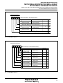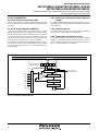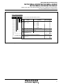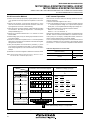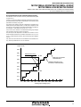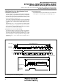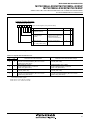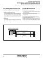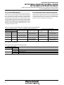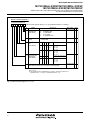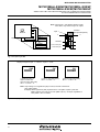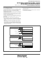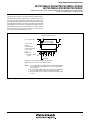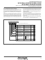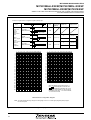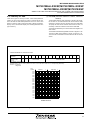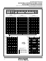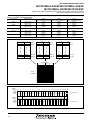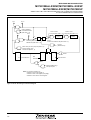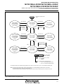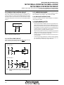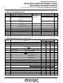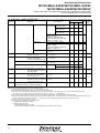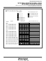
1
To all our customers
Regarding the change of names mentioned in the document, such as Mitsubishi
Electric and Mitsubishi XX, to Renesas Technology Corp.
The semiconductor operations of Hitachi and Mitsubishi Electric were transferred to Renesas
Technology Corporation on April 1st 2003. These operations include microcomputer, logic, analog
and discrete devices, and memory chips other than DRAMs (flash memory, SRAMs etc.)
Accordingly, although Mitsubishi Electric, Mitsubishi Electric Corporation, Mitsubishi
Semiconductors, and other Mitsubishi brand names are mentioned in the document, these names
have in fact all been changed to Renesas Technology Corp. Thank you for your understanding.
Except for our corporate trademark, logo and corporate statement, no changes whatsoever have been
made to the contents of the document, and these changes do not constitute any alteration to the
contents of the document itself.
Note : Mitsubishi Electric will continue the business operations of high frequency & optical devices
and power devices.
Renesas Technology Corp.
Customer Support Dept.
April 1, 2003
MITSUBISHI MICROCOMPUTERS
M37281MAH–XXXSP,M37281MFH–XXXSP
M37281MKH–XXXSP,M37281EKSP
SINGLE-CHIP 8-BIT CMOS MICROCOMPUTER with CLOSED CAPTION DECODER
and ON-SCREEN DISPLAY CONTROLLER
1. DESCRIPTION
The M37281MAH–XXXSP, M37281MFH–XXXSP and M37281MKHXXXSP are single-chip microcomputers designed with CMOS silicon
gate technology. They have a OSD function and a data slicer function, so it is useful for a channel selection system for TV with a closed
caption decoder.
The feautures of the M37281EKSP is similar to those of the
M37281MKH-XXXSP except that the chip has a built-in PROM which
can be written electrically. The difference between M37281MAH–
XXXSP, M37281MKH-XXXSP and M37281MFH-XXXSP are the ROM
size and RAM size. Accordingly, the following descriptions will be for
the M37281MKH-XXXSP.
2. FEATURES
●Number of basic instructions .................................................... 71
●Memory size
ROM .................. 40K bytes (M37281MAH-XXXSP)
60K bytes (M37281MFH-XXXSP)
80K bytes (M37281MKH-XXXSP,
M37281EKSP)
RAM ................... 1088 bytes (M37281MAH-XXXSP,
M37281MFH-XXXSP)
1536 bytes (M37281MKH-XXXSP,
M37281EKSP)
(*ROM correction memory included)
●Minimum instruction execution time
......................................... 0.5 µs (at 8 MHz oscillation frequency)
●Power source voltage ................................................. 5 V ± 10 %
●Subroutine nesting ............................................. 128 levels (Max.)
●Interrupts ....................................................... 19 types, 16 vectors
●8-bit timers .................................................................................. 6
●Programmable I/O ports (Ports P0, P1, P2, P30, P31) ............. 26
●Input ports (Ports P40–P46, P63, P64, P70–P72) ...................... 12
●Output ports (Ports P52–P55) ..................................................... 4
●LED drive ports ........................................................................... 2
●Serial I/O ............................................................ 8-bit ✕ 1 channel
●Multi-master I2C-BUS interface .............................. 1 (2 systems)
●A-D converter (8-bit resolution) .................................... 8 channels
●PWM output circuit ......................................................... 8-bit ✕ 8
●Power dissipation
In high-speed mode ......................................................... 165 mW
(at VCC = 5.5V, 8 MHz oscillation frequency, OSD on, and Data
slicer on)
In low-speed mode ......................................................... 0.33 mW
(at VCC = 5.5V, 32 kHz oscillation frequency)
Rev. 1.0
●ROM correction function ................................................ 2 vectors
●Closed caption data slicer
●OSD function
Display characters .... 32 characters ✕ 16 lines + RAM font (1 character)
(CC/OSD mode)(CDOSD mode)(RAM font)
Kinds of characters ......... 510 kinds
+ 62 kinds + 1 kind
(Coloring unit)
(a character)
(a dot)
(a dot)
Triple layer function .......................................................................
2 layers selected from CC/CDOSD/OSD mode + RAM font layer
Character display area .............. CC/CDOSD mode: 16 ✕ 26 dots
OSD mode/RAM font: 16 ✕ 20 dots
Kinds of character sizes .................... CC mode/RAM font: 4 kinds
OSD/CDOSD mode: 14 kinds
Kinds of character colors ..............................................................
64 colors (4 adjustment levels for each R, G, B)
Coloring unit ............ dot, character, character background, raster
Blanking output OUT1, OUT2
Display position
Horizontal: 256 levels
Vertical :1024 levels
(RAM font can be set independently)
Attribute ........................................................................................
CC mode: smooth italic, underline, flash, automatic solid space
OSD mode: border, shadow
Window/Blank function
3. APPLICATION
TV with a closed caption decoder
MITSUBISHI MICROCOMPUTERS
M37281MAH–XXXSP,M37281MFH–XXXSP
M37281MKH–XXXSP,M37281EKSP
SINGLE-CHIP 8-BIT CMOS MICROCOMPUTER with CLOSED CAPTION DECODER
and ON-SCREEN DISPLAY CONTROLLER
TABLE OF CONTENTS
1. DESCRIPTION .......................................................................... 1
9. PROGRAMMING NOTES ...................................................... 122
2. FEATURES ................................................................................ 1
10. ABSOLUTE MAXIMUM RATINGS ....................................... 123
3. APPLICATION ........................................................................... 1
11. RECOMMENDED OPERATING CONDITIONS ................... 123
4. PIN CONFIGURATION .............................................................. 3
12. ELECTRIC CHARACTERISTICS ........................................ 124
5. FUNCTIONAL BLOCK DIAGRAM ............................................. 4
13. ANALOG R, G, B OUTPUT CHARACTERISTICS ............... 126
6. PERFORMANCE OVERVIEW .................................................. 5
14. A-D CONVERTER CHARACTERISTICS ............................. 126
7. PIN DESCRIPTION ................................................................... 7
15. MULTI-MASTER I2C-BUS BUS LINE CHARACTERISTICS ......... 127
8. FUNCTIONAL DESCRIPTION ................................................ 11
16. PROM PROGRAMMING METHOD ..................................... 128
17. DATA REQUIRED FOR MASK ORDERS ............................ 129
18. APPENDIX ........................................................................... 130
19. PACKAGE OUTLINE ........................................................... 170
8.1 CENTRAL PROCESSING UNIT (CPU) ............................. 11
8.2 MEMORY .......................................................................... 12
8.3 INTERRUPTS .................................................................... 21
8.4 TIMERS ............................................................................. 26
8.5 SERIAL I/O ........................................................................ 30
8.6 MULTI-MASTER I2C-BUS INTERFACE ........................... 33
8.7 PWM OUTPUT CIRCUIT .................................................. 46
8.8 A-D CONVERTER ............................................................. 50
8.9 ROM CORRECTION FUNCTION ..................................... 54
8.10 DATA SLICER .................................................................. 55
8.11 OSD FUNCTIONS ........................................................... 66
8.11.1 Triple Layer OSD ................................................... 71
8.11.2 Display Position ..................................................... 74
8.11.3 Dot Size ................................................................. 78
8.11.4 Clock for OSD ....................................................... 79
8.11.5 Field Determination Display .................................. 81
8.11.6 Memory for OSD ................................................... 83
8.11.7 Character Color ..................................................... 91
8.11.8 Character Background Color ................................. 91
8.11.9 OUT1, OUT2 Signals ............................................ 95
8.11.10 Attribute ............................................................... 96
8.11.11 Automatic Solid Space Function ........................ 101
8.11.12 Multiline Display ................................................ 102
8.11.13 SPRITE OSD Function ...................................... 103
8.11.14 Window Function ............................................... 107
8.11.15 Blank Function ................................................. 108
8.11.16 Raster Coloring Function .................................. 113
8.11.17 Scan Mode ........................................................ 115
8.11.18 OSD Output Pin Control .................................... 116
8.12. SOFTWARE RUNAWAY DETECT FUNC-TION .......... 117
8.13. RESET CIRCUIT .......................................................... 118
8.14 CLOCK GENERATING CIRCUIT .................................. 119
8.15. DISPLAY OSCILLATION CIRCUIT ............................... 122
8.16. AUTO-CLEAR CIRCUIT ............................................... 122
8.17. ADDRESSING MODE .................................................. 122
8.18. MACHINE INSTRUCTIONS ......................................... 122
Rev. 1.0
2
MITSUBISHI MICROCOMPUTERS
M37281MAH–XXXSP,M37281MFH–XXXSP
M37281MKH–XXXSP,M37281EKSP
SINGLE-CHIP 8-BIT CMOS MICROCOMPUTER with CLOSED CAPTION DECODER
and ON-SCREEN DISPLAY CONTROLLER
4. PIN CONFIGURATION
HSYNC
1
52
P52/R/R1
VSYNC
2
51
P40/AD4
3
50
P53/G/G1
P54/B/B1
4
49
P55/OUT1
5
48
P04/PWM0
P43/TIM3
6
47
P05/PWM1
P24/AD3
7
46
P06/PWM2
P25/AD2
8
45
P07/PWM3
P20
P26/AD1
9
P27/AD5
P00/PWM4
10
P01/PWM5
12
P02/PWM6
P17/SIN/R0
13
P44/INT1
P45/SOUT
15
P46/SCLK
( )...M37281EKSP (AVCC
) NC
HLF/AD6
P72/(SIN)
17
P71/VHOLD
21
P70/CVIN
CNVSS
XIN
22
XOUT
VSS
11
14
16
18
19
20
M37281MAH-XXXSP, M37281MFH-XXXSP,
M37281MKH-XXXSP, M37281EKSP
P41/INT2
P42/TIM2
44
43
P21
42
P22
41
38
P23
P10/OUT2
P11/SCL1
P12/SCL2
37
P13/SDA1
36
P14/SDA2
P15/G0
40
39
35
34
33
32
P16/INT3/B0
P03/PWM7
31
P30/AD7
P31/AD8
23
30
RESET
24
29
25
28
P64/OSC2/X COUT
P63/OSC1/X CIN
26
27
VCC
Outline 52P4B
Note: Only 18th pin is NC pin of M37281MAH/
MFH/MKH-XXXSP. This pin is AVcc pin
of M37281EKSP. But NC pin of
M37281MAH/MFH/MKH-XXXSP is not
connect in the IC. You can apply to Vcc.
Fig. 4.1 Pin Configuration (Top View)
Rev. 1.0
3
14 34 35 36 37 38 39 40
I/O port P1
31 32
P1 (8)
Processor
status
register
PS (8)
RAM
Data bus
I/O ports
P30, P31
SDA2
SDA1
SCL2
SCL1
I2C-BUS interface
Multi-master
Accumulator
A (8)
Address bus
8-bit
arithmetic
and
logical unit
P3 (2)
35
Clock
generating
circuit
24
XIN XOUT
Y (8)
X (8)
23
P0 (8)
Stack
pointer
S (8)
ROM
TIM3
TIM2
SI/O
26
VSS CNVSS
I/O port P2
I/O port P0
22
Input ports P40–P46
17 16 15 6 5 4 3
P4 (7)
Timer 6
T6 (8)
Timer 5
T5 (8)
Timer 4
T4 (8)
Timer 3
T3 (8)
Timer 2
T2 (8)
Timer 1
T1 (8)
19
OSD circuit
Instruction
register (8)
Instruction
decoder
8-bit
PWM circuit
P6(2)
29
P5 (4)
Output port
P52–P55
49 50 51 52
2
1
Sync
signal input
OSD circuit
OSC2/XOUT
OSD circuit
28
OSC1/XCIN
Clock output for OSD/
sub-clock output
Input ports P63, P64
Clock input for OSD/
sub-clock input
A-D converter
Control signal
Data slicer
21
Timer count source
selection circuit
P7 (3)
20
SI/O (8)
10 9 8 7 41 42 43 44 45 46 47 48 33 13 12 11
P2 (8)
A-D
converter
Index
register
PCL (8)
PCH (8)
27
Index
register
counter
Program
18
Progam
counter
30
SIN
SCLK
SOUT
Pins for data slicer
CVIN VHOLD
HLF
INT1
INT2
Reset input (AV CC )
RESET NC VCC
PWM7
PWM6
PWM5
PWM4
PWM3
PWM2
PWM1
PWM0
Clock input Clock output
INT3
Input ports P70 – P72
OUT1
B
G
R
4
VSYNC
HSYNC
( )... M37281EKSP
MITSUBISHI MICROCOMPUTERS
M37281MAH–XXXSP,M37281MFH–XXXSP
M37281MKH–XXXSP,M37281EKSP
SINGLE-CHIP 8-BIT CMOS MICROCOMPUTER with CLOSED CAPTION DECODER
and ON-SCREEN DISPLAY CONTROLLER
5. FUNCTIONAL BLOCK DIAGRAM
Fig. 5.1 Functional Block Diagram of M37281
Rev. 1.0
MITSUBISHI MICROCOMPUTERS
M37281MAH–XXXSP,M37281MFH–XXXSP
M37281MKH–XXXSP,M37281EKSP
SINGLE-CHIP 8-BIT CMOS MICROCOMPUTER with CLOSED CAPTION DECODER
and ON-SCREEN DISPLAY CONTROLLER
6. PERFORMANCE OVERVIEW
Table 6.1 Performance Overview
Parameter
Number of basic instructions
Instruction execution time
Clock frequency
Memory size
ROM
RAM
Input/Output
ports
M37281MAH-XXXSP
M37281MFH-XXXSP
M37281MKH-XXXSP, M37281EKSP
M37281MAH-XXXSP,M37281MFH-XXXSP
M37281MKH-XXXSP, M37281EKSP
OSD ROM (character font)
OSD ROM (color dot font)
OSD RAM (SPRITE)
OSD RAM (character)
P00–P02, P04–P07
I/O
P03
P10, P15–P17
I/O
I/O
P11–P14
I/O
P2
P30, P31
P40–P44
I/O
I/O
Input
P45, P46
Input
P52–P55
P63
P64
Output
Input
Input
P70–P72
Serial I/O
Multi-master I2C-BUS interface
A-D converter
PWM output circuit
Timers
ROM correction function
Subroutine nesting
Interrupt
Clock generating circuit
Data slicer
Input
Functions
71
0.5 µs (the minimum instruction execution time, at 8 MHz oscillation frequency)
8 MHz (maximum)
40K bytes
60K bytes
80K bytes
1088 bytes (ROM correction memory included)
1536 bytes (ROM correction memory included)
20400 bytes
9672 bytes
120 bytes
1536 bytes
7-bit ✕ 1 (N-channel open-drain output structure, can be used as PWM
output pins)
1-bit ✕ 1 (CMOS input/output structure, can be used as PWM output pin)
4-bit ✕ 1 (CMOS input/output structure, can be used as OSD output pin,
INT input pin, serial input pin)
4-bit ✕ 1 (N-channel open-drain output structure, can be used as multimaster I2C-BUS interface)
8-bit ✕ 1 (CMOS input/output structure, can be used as A-D input pins)
2-bit ✕ 1 (CMOS input/output structure, can be used as A-D input pins)
5-bit ✕ 1 (can be used as A-D input pins, INT input pins, external clock input
pins for timer)
2-bit ✕ 1 (N-channel open-drain output structure when serial I/O is used,
can be used as serial I/O pins)
4-bit ✕ 1 (CMOS output structure, can be used as OSD output pins)
1-bit ✕ 1 (can be used as sub-clock input pin, OSD clock input pin)
1-bit ✕ 1 (CMOS output structure when LC is oscillating, can be used as
sub-clock output pin, OSD clock output pin)
3-bit ✕ 1 (can be used as data slicer input/output, serial input pin)
8-bit ✕ 1
1 (2 systems)
8 channels (8-bit resolution)
8-bit ✕ 8
8-bit timer ✕ 6
2 vectors
128 levels (maximum)
<19 types>
INT external interrupt ✕ 3, Internal timer interrupt ✕ 6, Serial I/O interrupt ✕
1, OSD interrupt ✕ 1, Multi-master I 2 C-BUS interface interrupt ✕ 1,
Data slicer interrupt ✕ 1, f(XIN)/4096 interrupt ✕ 1, SPRITE OSD interrupt ✕
1, VSYNC interrupt ✕ 1, A-D conversion interrupt ✕ 1, BRK instruction interrupt ✕ 1, Reset ✕ 1
2 built-in circuits (externally connected to a ceramic resonator or a quartzcrystal oscillator)
Built in
Rev. 1.0
5
MITSUBISHI MICROCOMPUTERS
M37281MAH–XXXSP,M37281MFH–XXXSP
M37281MKH–XXXSP,M37281EKSP
SINGLE-CHIP 8-BIT CMOS MICROCOMPUTER with CLOSED CAPTION DECODER
and ON-SCREEN DISPLAY CONTROLLER
Table 6.2 Performance Overview
OSD function
Parameter
Number of display characters
Dot structure
Kinds of characters
Kinds of character sizes
Character font coloring
Display position
Power source voltage
In high-speed
Power
mode
dissipation
In low-speed
mode
In stop mode
Operating temperature range
Device structure
Package
OSD ON
(Analog output)
OSD ON
(Digital output)
OSD OFF
OSD OFF
Data slicer
ON
Data slicer
OFF
Data slicer OFF
Data slicer
OFF
Functions
32 characters ✕ 16 lines
CC mode: 16 ✕ 26 dots (Character display area: 16 ✕ 20 dots)
OSD mode: 16 ✕ 20 dots
EXOSD mode: 16 ✕ 26 dots
SPRITE display: 16 ✕ 20 dots
CC/OSD mode: 510 kinds
CDOSD mode: 62 kinds
SPRITE display: 1 kind
CC mode: 4 kinds
OSD/CDOSD mode: 14 kinds
SPRITE display: 8 kinds
<CC mode>
1 screen : 8 kinds (per character unit)
<OSD mode>
1 screen : 15 kinds (per character unit)
<CDOSD mode> 1 screen : 8 kinds (per dot unit)
<SPRITE display> 1 screen : 8 kinds (per dot unit)
Horizontal: 256 levels, Vertical: 1024 levels
<SPRITE display> Horizontal: 2048 levels, Vertical: 1024 levels
5V ± 10%
275 mW typ. ( at oscillation frequency f(XIN) = 8 MHz, fOSC = 27 MHz)
165 mW typ. ( at oscillation frequency f(XIN) = 8 MHz, fOSC = 27 MHz )
82.5 mW typ. ( at oscillation frequency f(XIN) = 8 MHz)
0.33 mW typ. ( at oscillation frequency f(XCIN) = 32 kHz, f(XIN) = stop)
0.055 mW ( maximum )
–10 °C to 70 °C
CMOS silicon gate process
52-pin shrink plastic molded DIP
Rev. 1.0
6
MITSUBISHI MICROCOMPUTERS
M37281MAH–XXXSP,M37281MFH–XXXSP
M37281MKH–XXXSP,M37281EKSP
SINGLE-CHIP 8-BIT CMOS MICROCOMPUTER with CLOSED CAPTION DECODER
and ON-SCREEN DISPLAY CONTROLLER
7. PIN DESCRIPTION
Table 7.1 Pin Description
Pin
Name
Input/
Output
VCC,
(AVCC,)
VSS
CNVSS
RESET
Power source
Reset input
Input
XIN
Clock input
Input
XOUT
Clock output
P10/OUT2,
P11/SCL1,
P12/SCL2,
P13/SDA1,
P14/SDA2,
P15/G0,
P16/INT3/
B0,
P17/SIN/R0
P20–P23
P24/AD3–
P26/AD1,
P27/AD5
P30/AD7,
P31/AD8
P40/AD4,
P41/INT2,
P42/TIM2,
P43/TIM3,
P44/INT1,
P45/SOUT,
P46/SCLK
Apply voltage of 5 V ± 10 % (typical) to VCC (AVCC ) , and 0 V to VSS.
( ) ...M37281EKSP
Input
Connected to VSS.
To enter the reset state, the reset input pin must be kept at a LOW for 2 µs or more
(under normal VCC conditions).
If more time is needed for the quartz-crystal oscillator to stabilize, this LOW condition
should be maintained for the required time.
This chip has an internal clock generating circuit. To control generating frequency, an
external ceramic resonator or a quartz-crystal oscillator is connected between pins XIN
and XOUT. If an external clock is used, the clock source should be connected to the XIN
pin and the XOUT pin should be left open.
Port P0 is an 8-bit I/O port with direction register allowing each I/O bit to be individually
programmed as input or output. At reset, this port is set to input mode. The output structure
of P03 is CMOS output, that of P00–P02 and P04–P07 are N-channel open-drain output
(See note.)
Pins P00–P03 and P04–P07 are also used as 8-bit PWM output pins PWM4–PWM7 and
PWM0–PWM3 respectively. The output structure of PWM0–PWM6 is N-channel open-drain
output. And the output structure of PWM7 is CMOS output.
Port P1 is an 8-bit I/O port and has basically the same functions as port P0. The output
structure of P10 and P15–P17 is CMOS output, that of P11–P14 is N-channel open-drain
output (See note.)
Pin P10, P15–P17 are also used as OSD output pins OUT2, G0, B0, R0, respectively. The
output structure is CMOS output.
Pin P11–P14 are used as SCL1, SCL2, SDA1 and SDA2 respectively, when multi-master
I2C-BUS interface is used. The output structure is N-channel open-drain output.
Pin P16 is also used as INT extemal interrupt input pin INT3.
Input
Pin P17 is also used as serial I/O data input pin SIN.
CNVSS
P00/
I/O port P0
PWM4–
P02/PWM6,
P03/PWM7,
P04/
8-bit PWM output
PWM0–
P07/PWM3
Output
I/O
Output
I/O port P1
I/O
OSD output
Output
Multi-master
I2C-BUS interface
External interrupt
input
Serial I/O data
input
I/O port P2
Analog input
I/O port P3
Analog input
Input port P4
Analog input
External interrupt
input
External clock input
for timer
Serial I/O data
output
Serial I/O
synchronous clock
input/output
Functions
I/O
I/O
Input
I/O
Input
Input
Input
Input
Input
Output
I/O
Port P2 is an 8-bit I/O port and has basically the same functions as port P0. The output
structure is CMOS output (See note.)
Pins P24–P26, P27 are also used as analog input pins AD3–AD1, AD5 respectively.
Ports P30 and P31 are 2-bit I/O ports and have basically the same functions as port P0. The
output structure is CMOS output (See note.)
Pins P30, P31 are also used as analog input pins AD7, AD8 respectively.
Ports P40–P46 are a 7-bit input port.
Pin P40 is also used as analog input pin AD4.
Pins P41, P44 are also used as INT external interrupt input pins INT2, INT1.
Pins P42 and P43 are also used as INT external clock input pins TIM2, TIM3 for timer
respectively.
Pin P45 is used as serial I/O data output pin SOUT. The output structure is N-channel opendrain output.
Pin P46 is used as serial I/O synchronous clock input/output pin SCLK. The output structure
is N-channel open-drain output.
Rev. 1.0
7
MITSUBISHI MICROCOMPUTERS
M37281MAH–XXXSP,M37281MFH–XXXSP
M37281MKH–XXXSP,M37281EKSP
SINGLE-CHIP 8-BIT CMOS MICROCOMPUTER with CLOSED CAPTION DECODER
and ON-SCREEN DISPLAY CONTROLLER
Table 7.2 Pin Description (continued)
Pin
Name
Input/
Output
Output
Output
P52/R/R1,
P53/G/G1,
P54/B/B1,
P55/OUT1
Output port P5
OSD output
P63/OSC1/
XCIN,
P64/OSC2/
XCOUT
P70/CVIN,
P71/VHOLD,
P72/(SIN)
Input port P6
Clock input for OSD
Clock output for OSD
Sub-clock input
Sub-clock output
Input port P7
Input for data
slicer
Input
Input
Output
Input
Output
Input
Input
HLF/AD6
Serial I/O data input
I/O for data slicer
Input
I/O
HSYNC
VSYNC
Analog input
HSYNC input
VSYNC input
Input
Input
Input
Functions
Port P5 is a 4-bit output port. The output structure is CMOS output.
Pins P52–P55 are also used as OSD output pins R/R1, G/G1, B/B1, OUT1 respectively. At
R, G, B output, the output structure is analog output. At R1, G1, B1 and OUT1 output, the
output structure is CMOS output.
Ports P63 and P64 are 2-bit input port.
Pin P63 is also used as OSD clock input pin OSC1.
Pin P64 is also used as OSD clock output pin OSC2. The output structure is CMOS output.
Pin P63 is also used as sub-clock input pin XCIN.
Pin P64 is also used as sub-clock output pin XCOUT. The output structure is CMOS output.
Ports P70–P72 are 3-bit input port.
Pins P70, P71 are also used as data slicer input pins CVIN, VHOLD respectively. When using
data slicer, input composite video signal through a capacitor. Connect a capacitor between
VHOLD and VSS.
Pins P72 is also used as serial I/O data input pin SIN.
When using data slicer, connect a filter using of a capacitor and a resistor between HLF and
VSS.
This is an analog input pin AD6 .
This is a horizontal synchronous signal input for OSD.
This is a vertical synchronous signal input for OSD.
Note : Port Pi (i = 0 to 3) has the port Pi direction register (address 00C116 of zero page) which can be used to program each bit as an input (“0”) or an output (“1”).
The pins programmed as “1” in the direction register are output pins. When pins are programmed as “0,” they are input pins. When pins are programmed as
output pins, the output data are written into the port latch and then output. When data is read from the output pins, the output pin level is not read but the data
of the port latch is read. This allows a previously-output value to be read correctly even if the output “L” voltage has risen, for example, because a light emitting
diode was directly driven. The input pins float, so the values of the pins can be read. When data is written into the input pin, it is written only into the port latch,
while the pin remains in the floating state.
Rev. 1.0
8
MITSUBISHI MICROCOMPUTERS
M37281MAH–XXXSP,M37281MFH–XXXSP
M37281MKH–XXXSP,M37281EKSP
SINGLE-CHIP 8-BIT CMOS MICROCOMPUTER with CLOSED CAPTION DECODER
and ON-SCREEN DISPLAY CONTROLLER
P03, P10, P15–P17, P2, P30, P31
Direction register
Data bus
Port latch
CMOS output
Ports P03, P10, P15–P17,
P2, P30, P31
Note : Each port is also used as follows :
P00 : PWM7
P10 : OUT2
P15 : G0
P16 : INT3/B0
P17 : SIN/R0
P24–P26 : AD3–AD1
P27 : AD5
P30 : AD7
P31 : AD8
P00–P02, P04–P07
N-channel open-drain output
Direction register
Ports P00–P02, P04–P07
Data bus
Port latch
Note1 : Each port is also used as follows :
P0 0–P02 : PWM4–PWM6
P04–P07 : PWM0–PWM3
2 : M37281EKSP, does not have
the diode side with VCC.
P11–P14
N-channel open-drain output
Direction register
Port P11-P14
Data bus
Port latch
Note : Each port is also used as follows :
P11 : SCL1
P12 : SCL2
P13 : SDA1
P14 : SDA2
Fig. 7.1 I/O Pin Block Diagram (1)
Rev. 1.0
9
MITSUBISHI MICROCOMPUTERS
M37281MAH–XXXSP,M37281MFH–XXXSP
M37281MKH–XXXSP,M37281EKSP
SINGLE-CHIP 8-BIT CMOS MICROCOMPUTER with CLOSED CAPTION DECODER
and ON-SCREEN DISPLAY CONTROLLER
SOUT, SCLK
N-channel open-drain output
Direction register
Ports P45, P46
Note : Each pin is also used
as follows :
P45 : SOUT
P46 : SCLK
Data bus
HSYNC, VSYNC
Port P55
Schmidt input
Internal circuit
CMOS output
HSYNC, VSYNC
Internal circuit
Port P55
Note : Port P55 is also used
as pin OUT1.
Ports P40–P44
Input
Data bus
Ports P52–P54
Ports P40–P44
Note : Each port is also used as follows :
P40 : AD4
P41 : INT2
P42 : TIM2
P43 : TIM3
P44 : INT1
Internal circuit
Output
Ports P52–P54
Note : Each port is also used as follows :
P52 : R/R1
P53 : G/G1
P54 : B/B1
Fig. 7.2 I/O Pin Block Diagram (2)
Rev. 1.0
10
MITSUBISHI MICROCOMPUTERS
M37281MAH–XXXSP,M37281MFH–XXXSP
M37281MKH–XXXSP,M37281EKSP
SINGLE-CHIP 8-BIT CMOS MICROCOMPUTER with CLOSED CAPTION DECODER
and ON-SCREEN DISPLAY CONTROLLER
8. FUNCTIONAL DESCRIPTION
8.1. CENTRAL PROCESSING UNIT (CPU)
This microcomputer uses the standard 740 Family instruction set.
Refer to the table of 740 Family addressing modes and machine
instructions or the SERIES 740 <Software> User’s Manual for details on the instruction set.
Machine-resident 740 Family instructions are as follows:
The FST, SLW instruction cannot be used.
The MUL, DIV, WIT and STP instructions can be used.
8.1.1 CPU Mode Register
The CPU mode register contains the stack page selection bit and
internal system clock selection bit. The CPU mode register is allocated at address 00FB16.
CPU Mode Register
b7 b6 b5 b4 b3 b2 b1 b0
1 1
0 0
CPU mode register (CM) [Address 00FB16]
B
Name
P
r
o
c
e
s
s
or mode bits
0, 1
(CM0, CM1)
2 Stack page selection
bit (CM2) (See note)
Functions
b1 b0
0
0
1
1
0: 0 page
1: 1 page
0: LOW drive
1: HIGH drive
6 Main Clock (XIN–XOUT) 0: Oscillating
stop bit
1: Stopped
(CM6)
7 Internal system clock
selection bit
(CM7)
0
R W
1
R W
1
R W
1
R W
0
R W
0
R W
0: Single-chip mode
1:
0:
Not available
1:
3, 4 Fix these bits to “1.”
5 XCOUT drivability
selection bit (CM5)
After reset R W
0: XIN–XOUT selected
(high-speed mode)
1: XCIN–XCOUT selected
(low-speed mode)
Note: This bit is set to “1” after the reset release.
Fig. 8.1.1 CPU Mode Register
Rev. 1.0
11
MITSUBISHI MICROCOMPUTERS
M37281MAH–XXXSP,M37281MFH–XXXSP
M37281MKH–XXXSP,M37281EKSP
SINGLE-CHIP 8-BIT CMOS MICROCOMPUTER with CLOSED CAPTION DECODER
and ON-SCREEN DISPLAY CONTROLLER
8.2 MEMORY
8.2.1 Special Function Register (SFR) Area
8.2.6 Interrupt Vector Area
The interrupt vector area contains reset and interrupt vectors.
The special function register (SFR) area in the zero page contains
control registers such as I/O ports and timers.
8.2.2 RAM
RAM is used for data storage and for stack area of subroutine calls
and interrupts.
8.2.3 ROM
The M37281MAH-XXXSP has 40K-byte program area and
M37281MFH-XXXSP has 60K-byte program area. The M37281MKH
-XXXSP has 56K-byte program area and 24K-byte data-dedicated
area. For the M37281EKSP, the two area (60K, 24K + 56K) can be
swithed each other by setting the bank control register.
8.2.7 Zero Page
The 256 bytes from addresses 000016 to 00FF16 are called the zero
page area. The internal RAM and the special function registers (SFR)
are allocated to this area.
The zero page addressing mode can be used to specify memory and
register addresses in the zero page area. Access to this area with
only 2 bytes is possible in the zero page addressing mode.
8.2.8 Special Page
8.2.4 OSD RAM
The 256 bytes from addresses FF0016 to FFFF16 are called the special page area. The special page addressing mode can be used to
specify memory addresses in the special page area. Access to this
area with only 2 bytes is possible in the special page addressing
mode.
RAM for display is used for specifying the character codes and colors to display.
8.2.9 ROM Correction Vector
8.2.5 OSD ROM
This is used as the program jump destination addresses for ROM
correction.
ROM for display is used for storing character data.
■ M37281MKH-XXXSP, M37281EKSP
000016
1000016
Not used
RAM
(1536 bytes)
00BF16
00C016
00FF16
010016
1080016
Zero page
SFR1 area
OSD ROM
(Character font)
(20400 bytes)
020016
025816
SFR2 area
Not used
02C016
ROM correction function
Vector 1: address 02C016
Vector 2: address 02E016
02E016
157FF16
Not used
OSD RAM (SPRITE)
(120 bytes)
(Note 1)
06FF16
070016
1800016
07A716
Not used
OSD RAM (Character)
(1536 bytes)
(Note 2)
OSD ROM
(Color dot font)
(9672 bytes)
080016
0FFF16
100016
1ACFF16
Extra area
200016
Not used
1B00016
ROM
(60K bytes)
Bank 11
1C00016
Bank 12
Expansion ROM
(20K bytes)
1D00016
1E00016
FF0016
FFDE16
FFFF16
Interrupt vector area
Special page
1F00016
Bank 13
Bank 14
Bank 15
1FFFF16
Notes 1: Refer to Table 8.11.6 OSD RAM (SPRITE).
2: Tables 8.11.4 and 8.11.5 OSD RAM (Character).
Fig. 8.2.1 Memory Map (M37281MKH-XXXSP, M37281EKSP)
Rev. 1.0
12
MITSUBISHI MICROCOMPUTERS
M37281MAH–XXXSP,M37281MFH–XXXSP
M37281MKH–XXXSP,M37281EKSP
SINGLE-CHIP 8-BIT CMOS MICROCOMPUTER with CLOSED CAPTION DECODER
and ON-SCREEN DISPLAY CONTROLLER
■ M37281MAH-XXXSP, M37281MFH-XXXSP
000016
M37281MAH-XXXSP,
M37281MFH-XXXSP
RAM
(1088 bytes)
00BF16
00C016
00FF16
010016
1000016
Zero page
SFR1 area
OSD ROM
(Character font)
(20400 bytes)
020016
025816
Not used
1080016
SFR2 area
Not used
02C016
ROM correction function
Vector 1: address 02C016
Vector 2: address 02E016
02E016
157FF16
053F16
Not used
Not used
OSD RAM (SPRITE)
(120 bytes)
(Note 1)
070016
1800016
07A716
Extra area
OSD ROM
(Color dot font)
(9672 bytes)
080016
OSD RAM (Character)
(1536 bytes)
(Note 2)
0FFF16
100016
1ACFF16
M37281MFH-XXXSP
ROM
(60K bytes)
600016
Not used
M37281MAH-XXXSP
ROM
(40K bytes)
FF0016
FFDE16
FFFF16
Interrupt vector area
Special page
Notes 1: Refer to Table 8.11.6 OSD RAM (SPRITE).
2 : Tables 8.11.4 and 8.11.5 OSD RAM (Character).
Fig. 8.2.2 Memory Map (M37281MAH-XXXSP,M37281MFH-XXXSP)
Rev. 1.0
13
MITSUBISHI MICROCOMPUTERS
M37281MAH–XXXSP,M37281MFH–XXXSP
M37281MKH–XXXSP,M37281EKSP
SINGLE-CHIP 8-BIT CMOS MICROCOMPUTER with CLOSED CAPTION DECODER
and ON-SCREEN DISPLAY CONTROLLER
8.2.10 Expansion ROM (only M37281MKHXXXSP/M37281EKSP)
The M37281MKH-XXXSP/M37281EKSP can use 5-bank (total 20K
bytes) expansion ROM (4K bytes each bank) by setting the bank
register.
The expansion ROM is assigned to address 1B00016 to 1FFFF16.
The contents of each bank in the expansion ROM are read by setting
the bank register and accessing addresses 100016 to 1FFF16. As the
expansion ROM is not programmable, use it as data-dedicated area.
When using the expansion ROM area, the internal ROM at addresses
100016 to 1FFF16 (extra area) is not also programmable.
Notes 1: When using the expansion ROM (BK7 = “1”), the ROM correction
function do not operate for addresses 100016 to 1FFF16.
2: When using the emulator MCU (M37281ERSS), as addresses 100016
to FFFF16 can be emulated by setting bit 7 of the bank control register to “0,” the expansion ROM cannot be used. Addresses 200016 to
FFFF16 can be emulated by setting it to “1.” The data in specified
area by the bank selection bits can be read by accessing addresses
100016 to 1FFF16.
3: When using the emulator MCU, the expansion ROM and the extra
area cannot be emulated by setting bit 7 of the bank control register
to “1.” Therefore, write the data to this area before using.
4: For the M37281MKH-XXXSP, fix bit 7 of the bank control register to
“1.” For M37281MAH-XXXSP and M37281MFH-XXXSP, fix the address 00ED16 to “0016.”
Bank Control Register
b7 b6 b5 b4 b3 b2 b1 b0
0 0
Bank control register (BK) [Address 00ED16]
B
0
to
3
Name
Functions
Bank
Bank number is selected (bank 11 to 15)
selection bits
(BK0 to BK3)
4, 5 Fix these bits to “0.”
6, 7 Bank control
bits
(BK6, BK7)
b7 b6 Bank ROM Address 100016 level
access
Read out from extra area
0 ✕ Not used
(programmable)
Read out the data
1 0 Used
from area specified by
the bank selection bits
Read out from extra area
1 1 Used
(data-dedicated)
After reset R W
0
R W
0
R W
0
R W
Fig. 8.2.3 Bank Control Register
Rev. 1.0
14
MITSUBISHI MICROCOMPUTERS
M37281MAH–XXXSP,M37281MFH–XXXSP
M37281MKH–XXXSP,M37281EKSP
SINGLE-CHIP 8-BIT CMOS MICROCOMPUTER with CLOSED CAPTION DECODER
and ON-SCREEN DISPLAY CONTROLLER
■ SFR1 area (addresses C016 to DF16)
<Bit allocation>
:
<State immediately after reset>
0 : “0” immediately after reset
Function bit
:
Name
1 : “1” immediately after reset
: No function bit
? : Indeterminate immediately
after reset
0 : Fix to this bit to “0”
(do not write to “1”)
1 : Fix to this bit to “1”
(do not write to “0”)
Address
Register
Bit allocation
State immediately after reset
b7
C016
C116
C216
C316
C416
C516
C616
C716
C816
C916
CA16
CB16
CC16
CD16
CE16
CF16
D016
D116
D216
D316
D416
D516
D616
D716
D816
D916
DA16
DB16
DC16
DD16
DE16
DF16
b0 b7
b0
Port P0 (P0)
Port P0 direction register (D0)
Port P1 (P1)
Port P1 direction register (D1)
Port P2 (P2)
Port P2 direction register (D2)
Port P3 (P3)
Port P3 direction register (D3)
P6IM T3CS
Port P4 (P4)
Port P4 direction register (D4)
0
Port P5 (P5)
OSD port control register (PF)
Port P6 (P6)
Port P7 (P7)
OSD control register 1 (OC 1)
Horizontal position register (HP)
0
OUT2OUT1
B
G
R
RGB
2BIT
0
0
OC17OC16OC15OC14OC13OC12OC11OC10
HP7 HP6 HP5 HP4 HP3 HP2 HP1 HP0
Block control register 1 (BC1)
BC16 BC15 BC14 BC13 BC12 BC11 BC10
Block control register 2 (BC2)
BC26 BC25 BC24 BC23 BC22 BC21 BC20
Block control register 3 (BC3)
BC36 BC35 BC34 BC33 BC32 BC31 BC30
Block control register 4 (BC4)
BC46 BC45 BC44 BC43 BC42 BC41 BC40
Block control register 5 (BC5)
BC56 BC55 BC54 BC53 BC52 BC51 BC50
Block control register 6 (BC6)
BC66 BC65 BC64 BC63 BC62 BC61 BC60
Block control register 7 (BC7)
BC76 BC75 BC74 BC73 BC72 BC71 BC70
Block control register 8 (BC8)
BC86 BC85 BC84 BC83 BC82 BC81 BC80
Block control register 9 (BC9)
BC96 BC95 BC94 BC93 BC92 BC91 BC90
Block control register 10 (BC10)
BC106 BC105 BC104 BC103 BC102 BC101 BC100
Block control register 11 (BC11)
BC116 BC115 BC114 BC113 BC112 BC111 BC110
Block control register 12 (BC12)
Block control register 13 (BC13)
Block control register 14 (BC14)
Block control register 15 (BC15)
Block control register 16 (BC16)
BC126 BC125 BC124 BC123 BC122 BC121 BC120
BC136 BC135 BC13 BC133 BC132 BC131 BC130
BC 6 BC 5 BC4 4 BC 3 BC 2 BC 1 BC 0
14
14
14
14
14
14
14
BC156 BC155 BC154 BC153 BC152 BC151 BC150
BC166 BC165 BC164 BC163 BC162 BC161 BC160
0
0
?
0016
?
0016
?
0016
?
0016
?
0016
?
0016
?
0 0
0016
0016
?
?
?
?
?
?
?
?
?
?
?
?
?
?
?
?
?
?
?
Fig. 8.2.4 Memory Map of Special Function Register 1 (SFR1) (1)
Rev. 1.0
15
MITSUBISHI MICROCOMPUTERS
M37281MAH–XXXSP,M37281MFH–XXXSP
M37281MKH–XXXSP,M37281EKSP
SINGLE-CHIP 8-BIT CMOS MICROCOMPUTER with CLOSED CAPTION DECODER
and ON-SCREEN DISPLAY CONTROLLER
■ SFR1 area (addresses E016 to FF16)
<Bit allocation>
:
Name
<State immediately after reset>
0 : “0” immediately after reset
Function bit
:
1 : “1” immediately after reset
: No function bit
? : Indeterminate immediately
after reset
0 : Fix to this bit to “0”
(do not write to “1”)
1 : Fix to this bit to “1”
(do not write to “0”)
Address
Register
Bit allocation
State immediately after reset
b0 b7
b7
E016
E116
E216
E316
E416
E516
E616
E716
E816
E916
EA16
EB16
EC16
ED16
EE16
EF16
F016
F116
F216
F316
F416
F516
F616
F716
F816
F916
FA16
FB16
FC16
FD16
FE16
FF16
Data slicer control register 1 (DSC1)
Data slicer control register 2 (DSC2)
Caption data register 1 (CD1)
0
0
0
0
0
0
0
DSC25 DSC24 DSC23
DSC20
CDH17CDH16CDH15CDH14CDH13CDH12CDH11CDH10
Caption data register 3 (CD3)
CDL27 CDL26 CDL25 CDL24 CDL23 CDL22 CDL21 CDL20
Caption data register 4 (CD4)
CDH27CDH26CDH25CDH24CDH23CDH22CDH21CDH20
Caption Position register (CPS)
CPS7 CPS6 CPS5 CPS4 CPS3 CPS2 CPS1 CPS0
0
?
0
0
?
0
0
?
0
?
0
0016
0016
Data slicer test register 2
Data slicer test register 1
Sync signal counter register (HC)
HC5 HC4 HC3 HC2 HC1 HC0
Clock run-in detect register (CRD)
CRD7 CRD6 CRD5 CRD4 CRD3
Data clock position register (DPS)
DPS7 DPS6 DPS5 DPS4 DPS3
Bank control register (BK)
A-D conversion register (AD)
A-D control register (ADCON)
Timer 1 (T1)
Timer 2 (T2)
Timer 3 (T3)
Timer 4 (T4)
Timer mode register 1 (TM1)
Timer mode register 2 (TM2)
I2C data shift register (S0)
I2C address register (S0D)
I2C status register (S1)
I2C control register (S1D)
I2C clock control register (S2)
BK7 BK6
0
0
0
0
0
0
1
BK3 BK2 BK1 BK0
ADVREF ADSTR ADIN2 ADIN1 ADIN0
TM17 TM16 TM15 TM14 TM13 TM12 TM11 TM10
TM27 TM26 TM25 TM24 TM23 TM22 TM21 TM20
D7
D6
D5
D4
D3
D2
D1
D0
SAD6 SAD5 SAD4 SAD3 SAD2 SAD1 SAD0 RBW
MST TRX BB
PIN
BSEL1 BSEL0 10BIT
ALS ESO BC2 BC1 BC0
SAD
ACK ACK
BIT
FAST
MODE
AL AAS AD0 LRB
CCR4 CCR3 CCR2 CCR1 CCR0
CM7 CM6 CM5 1
CPU mode register (CM)
1 CM2 0 0
Interrupt request register 1 (IREQ1)
ADR VSCR OSDR TM4R TM3R TM2R TM1R
Interrupt control register 2 (ICON2)
?
CDL17 CDL16 CDL15 CDL14 CDL13 CDL12 CDL11 CDL10
Caption data register 2 (CD2)
Interrupt request register 2 (IREQ2)
Interrupt control register 1 (ICON1)
b0
DSC12 DSC11 DSC10
0
TM56R
CK0 CKR SIOR DSR IN1R
IICR IN2R
ADE VSCEOSDE TM4E TM3E TM2E TM1E
TM56S TM56E
IICE IN2E CKE SIOE DSE IN1E
0
0
0
0016
0 ?
0016
0016
0016
0016
0 0
0016
0016
? ?
0016
0916
?
0016
?
0 1
FF16
0716
FF16
0716
0016
0016
?
0016
1 0
0016
0016
3C16
0016
0016
0016
0016
?
0
?
0
0
0
?
?
?
0
0
0
0
0
?
Fig. 8.2.5 Memory Map of Special Function Register 1 (SFR2) (2)
Rev. 1.0
16
MITSUBISHI MICROCOMPUTERS
M37281MAH–XXXSP,M37281MFH–XXXSP
M37281MKH–XXXSP,M37281EKSP
SINGLE-CHIP 8-BIT CMOS MICROCOMPUTER with CLOSED CAPTION DECODER
and ON-SCREEN DISPLAY CONTROLLER
■ SFR2 area (addresses 20016 to 21F16)
<Bit allocation>
:
Name
<State immediately after reset>
0 : “0” immediately after reset
Function bit
:
1 : “1” immediately after reset
: No function bit
? : Indeterminate immediately
after reset
0 : Fix to this bit to “0”
(do not write to “1”)
1 : Fix to this bit to “1”
(do not write to “0”)
Address
Register
20016
20116
20216
20316
20416
20516
20516
20716
20816
20916
20A16
20B16
20C16
20D16
20E16
20F16
21016
21116
21216
21316
21416
21516
21616
21716
21816
21916
21A16
21B16
21C16
21D16
21E16
21F16
State immediately after reset
Bit allocation
b7
b0 b7
PWM0 register (PWM0)
PWM1 register (PWM1)
PWM2 register (PWM2)
PWM3 register (PWM3)
PWM4 register (PWM4)
PWM5 register (PWM5)
PWM6 register (PWM6)
PWM7 register (PWM7)
PWM mode register 1 (PN)
PWM mode register 2 (PW)
PN4 PN3
0
PN0
PW6 PW5 PW4 PW3 PW2 PW1 PW0
ROM correction address 1 (high-order)
ROM correction address 1 (low-order)
ROM correction address 2 (high-order)
ROM correction address 2 (low-order)
ROM correction enable register (RCR)
Test register
Interrupt input polarity register (IP)
Serial I/O mode register (SM)
Serial I/O register (SIO)
OSD control register 2(OC2)
Clock control register (CS)
I/O polarity control register (PC)
Raster color register (RC)
OSD control register 3(OC3)
AD/INT3
SEL
RE 5
A
D/I/NIN
AD
T3T3
PIN
OTL3
S
3
SEELL
T
AD/INT3IPNO
S
M6
SEL
3
L
RE5 POL2 PROEL31 RE2 RE1
R0E3 R0
E2
0016
RRCER11 RCR0
RM
S
E55 SM4 S
RM
E33 S
RM
E22 S
RM
E11 SM0
PO
L
OC27 OC26 OC25 OC24 OC23 OC12 OC21 OC20
AD/INT3
SEL
AD/INT3INT
P C7 P
C6 R
PC
E 5 P C4
SEL
3
T
AD/INT3IPNO
RC7
RC6
RC5
R
E5 RC4
EL
3
L
0
0
0
0
RS
E2 C
RS
E 1 CS 0
C
RE 3 P
RC
E2 P
RC
E 1 P C0
RC3
RC2
RC1
R
E3 R
E2 R
E1 RC0
PC
O36 OC35 OC34 O
OC37 O
RC
E33 O
RC
E2
32 O
RC
E1
31 OC30
L
Timer 5 (TM5)
Timer 6 (TM6)
Top border control register 1 (TB1)
TB17 TB16 TB15 TB14 TB13 TB12 TB11 TB10
Bottom border control register 1 (BB1)
BB17 BB16 BB15 BB14 BB13 BB12 BB11 BB10
Top border control register 2 (TB2)
Bottom border control register 2 (BB2)
BB21 BB20
TB21 TB20
b0
?
?
?
?
?
?
?
?
?
?
0016
0016
0016
0016
0016
0016
0016
0016
0016
0016
?
0016
0016
8016
0016
0016
FF16
0716
?
?
?
?
Fig. 8.2.6 Memory Map of Special Function Register 2 (SFR2) (1)
Rev. 1.0
17
MITSUBISHI MICROCOMPUTERS
M37281MAH–XXXSP,M37281MFH–XXXSP
M37281MKH–XXXSP,M37281EKSP
SINGLE-CHIP 8-BIT CMOS MICROCOMPUTER with CLOSED CAPTION DECODER
and ON-SCREEN DISPLAY CONTROLLER
■ SFR2 area (addresses 22016 to 23F16)
<State immediately after reset>
<Bit allocation>
:
Name
0 : “0” immediately after reset
Function bit
:
1 : “1” immediately after reset
: No function bit
? : Indeterminate immediately
after reset
0 : Fix to this bit to “0”
(do not write to “1”)
1 : Fix to this bit to “1”
(do not write to “0”)
Address
Register
b7
22016
22116
22216
22316
22416
22516
22616
22716
22816
22916
22A16
22B16
22C16
22D16
22E16
22F16
23016
23116
23216
23316
23416
23516
23616
23716
23816
23916
23A16
23B16
23C16
23D16
23E16
23F16
Vertical position register 11 (VP11)
Vertical position register 12 (VP12)
Vertical position register 13 (VP13)
Bit allocation
State immediately after reset
b0 b7
VP117 VP116 VP115 VP114 VP113 VP112 VP111VP1 0
1
VP127 VP126 VP125 VP124 VP123 VP122 VP121VP1 0
2
VP137 VP136 VP135 VP134 VP133 VP132 VP131VP1 0
3
Vertical position register 14 (VP14)
VP147 VP146 VP145 VP144 VP143 VP142 VP141VP1 0
4
Vertical position register 15 (VP15)
Vertical position register 16 (VP16)
Vertical position register 17 (VP17)
VP157 VP156 VP155 VP154 VP153 VP152 VP151VP1 0
5
Vertical position register 18 (VP18)
Vertical position register 19 (VP19)
VP187 VP186 VP185 VP184 VP183 VP182 VP181VP1 0
8
Vertical position register 110 (VP110)
VP1107 VP1106 VP1105 VP1104 VP1103 VP1102 VP1101VP1 0
10
Vertical position register 111 (VP111)
Vertical position register 112 (VP112)
VP1117 VP1116 VP1115 VP1114 VP1113 VP1112 VP1111VP1 0
11
Vertical position register 113 (VP113)
Vertical position register 114 (VP114)
Vertical position register 115 (VP115)
Vertical position register 116 (VP116)
Vertical position register 21 (VP21)
VP167 VP166 VP165 VP164 VP163 VP162 VP161VP1 0
6
VP177 VP176 VP175 VP174 VP173 VP172 VP171VP1 0
7
VP197 VP196 VP195 VP194 VP193 VP192 VP191VP1 0
9
VP1127 VP1126 VP1125 VP1124 VP1123 VP1122 VP1121VP1 0
12
VP1137 VP1136 VP1135 VP1134 VP1133 VP1132 VP1131 VP1130
VP1147 VP1146 VP1145 VP1144 VP1143 VP1142 VP1141 VP1140
VP1157 VP1156 VP1155 VP1154 VP1153 VP1152 VP1151 VP1150
VP1167 VP1166 VP1165 VP1164 VP1163 VP1162 VP1161 VP1160
Vertical position register 22 (VP22)
VP211 VP210
VP221 VP220
Vertical position register 23 (VP23)
VP231 VP230
Vertical position register 24 (VP24)
VP241 VP240
Vertical position register 25 (VP25)
Vertical position register 26 (VP26)
VP251 VP250
VP261 VP260
Vertical position register 27 (VP27)
VP271 VP270
Vertical position register 28 (VP28)
Vertical position register 29 (VP29)
VP291 VP290
VP281 VP280
Vertical position register 210 (VP210)
VP2101 VP2100
Vertical position register 211 (VP211)
Vertical position register 212 (VP212)
VP2111 VP2110
VP2121 VP2120
Vertical position register 213 (VP213)
VP2131 VP2130
Vertical position register 214 (VP214)
VP2141 VP2140
Vertical position register 215 (VP215)
Vertical position register 216 (VP216)
VP2151 VP2150
VP2161 VP2160
b0
?
?
?
?
?
?
?
?
?
?
?
?
?
?
?
?
?
?
?
?
?
?
?
?
?
?
?
?
?
?
?
?
Fig. 8.2.7 Memory Map of Special Function Register 2 (SFR2) (2)
Rev. 1.0
18
MITSUBISHI MICROCOMPUTERS
M37281MAH–XXXSP,M37281MFH–XXXSP
M37281MKH–XXXSP,M37281EKSP
SINGLE-CHIP 8-BIT CMOS MICROCOMPUTER with CLOSED CAPTION DECODER
and ON-SCREEN DISPLAY CONTROLLER
■ SFR2 area (addresses 24016 to 25816)
<State immediately after reset >
<Bit allocation>
:
Name
0 : “0” immediately after reset
Function bit
:
1 : “1” immediately after reset
: No function bit
? : Indeterminate immediately
after reset
0 : Fix to this bit to “0”
(do not write to “1”)
1 : Fix to this bit to “1”
(do not write to “0”)
Address
Register
State immediately after reset
Bit allocation
b7
24016
24116
24216
24316
24416
24516
24616
24716
24816
24916
24A16
24B16
24C16
24D16
24E16
24F16
25016
25116
25216
25316
25416
25516
25616
25716
25816
b0 b7
Color pallet register 1 (CR1)
Color pallet register 2 (CR2)
CR16 CR15 CR14 CR13 CR12 CR11 CR10
Color pallet register 3 (CR3)
Color pallet register 4 (CR4)
CR36 CR35 CR34 CR33 CR32 CR31 CR30
Color pallet register 5 (CR5)
CR56 CR55 CR54 CR53 CR52 CR51 CR50
Color pallet register 6 (CR6)
CR66 CR65 CR64 CR63 CR62 CR61 CR60
Color pallet register 7 (CR7)
CR76 CR75 CR74 CR73 CR72 CR71 CR70
Color pallet register 9 (CR9)
Color pallet register10 (CR10)
CR 10 6 CR 10 5 CR 10 4 CR 10 3 CR 10 2 CR 10 1 CR 10 0
Color pallet register 11 (CR11)
CR 11 6 CR 11 5 CR 11 4 CR 11 3 CR 11 2 CR 11 1 CR 11 0
Color pallet register 12 (CR12)
CR 12 6 CR 12 5 CR 12 4 CR 12 3 CR 12 2 CR 12 1 CR 12 0
Color pallet register 13 (CR13)
CR 13 6 CR 13 5 CR 13 4 CR 13 3 CR 13 2 CR 13 1 CR 13 0
Color pallet register 14 (CR14)
Color pallet register 15 (CR15)
Left border control register 1 (LB1)
CR 14 6 CR 14 5 CR 14 4 CR 14 3 CR 14 2 CR 14 1 CR 14 0
LB17 LB16 LB15 LB14 LB13 LB12 LB11 LB10
Left border control register 2 (LB2)
LB22 LB21 LB20
b0
CR26 CR25 CR24 CR23 CR22 CR21 CR20
CR46 CR45 CR44 CR43 CR42 CR41 CR40
CR96 CR95 CR94 CR93 CR92 CR91 CR90
CR 15 6 CR 15 5 CR 15 4 CR 15 3 CR 15 2 CR 15 1 CR 15 0
Right border control register 1 (RB1)
Right border control register 2 (RB2)
RB17 RB16 RB15 RB14 RB13 RB12 RB11 RB10
SPRITE vertical position register 1 (VS1)
VS17 VS16 VS15 VS14 VS13 VS12 VS11 VS10
SPRITE vertical position register 2 (VS2)
VS21 VS20
RB22 RB21 RB20
SPRITE horizontal position register 1 (HS1) HS17 HS16 HS15 HS14 HS13 HS12 HS11 HS10
SPRITE horizontal position register 2 (HS2)
SPRITE OSD control register (SC)
HS22 HS21 HS20
SC5
SC4
SC3
SC2
SC1
SC0
0
0
0
?
?
?
?
?
?
?
?
?
?
?
?
?
?
?
?
0116
0016
FF16
0716
?
0016
?
0 0
0016
?
?
?
Fig. 8.2.8 Memory Map of Special Function Register 2 (SFR2) (3)
Rev. 1.0
19
MITSUBISHI MICROCOMPUTERS
M37281MAH–XXXSP,M37281MFH–XXXSP
M37281MKH–XXXSP,M37281EKSP
SINGLE-CHIP 8-BIT CMOS MICROCOMPUTER with CLOSED CAPTION DECODER
and ON-SCREEN DISPLAY CONTROLLER
<State immediately after reset>
<Bit allocation>
:
Name
0 : “0” immediately after reset
Function bit
:
1 : “1” immediately after reset
: No function bit
? : Indeterminate immediately
after reset
0 : Fix to this bit to “0”
(do not write to “1”)
1 : Fix to this bit to “1”
(do not write to “0”)
Register
Bit allocation
State immediately after reset
b0 b7
b7
Processor status register (PS)
Program counter (PCH)
N
V
T
B
D
I
Z
C
Program counter (PCL)
b0
?
? ? ? ? 1 ? ?
Contents of address FFFF16
Contents of address FFFE16
Fig. 8.2.9 Internal State of Processor Status Register and Program Counter at Reset
Rev. 1.0
20
MITSUBISHI MICROCOMPUTERS
M37281MAH–XXXSP,M37281MFH–XXXSP
M37281MKH–XXXSP,M37281EKSP
SINGLE-CHIP 8-BIT CMOS MICROCOMPUTER with CLOSED CAPTION DECODER
and ON-SCREEN DISPLAY CONTROLLER
8.3 INTERRUPTS
Interrupts can be caused by 19 different sources consisting of 3 external, 14 internal, 1 software, and reset. Interrupts are vectored interrupts with priorities as shown in Table 8.3.1. Reset is also included
in the table because its operation is similar to an interrupt.
When an interrupt is accepted,
① The contents of the program counter and processor status register
are automatically stored into the stack.
➁ The interrupt disable flag I is set to “1” and the corresponding
interrupt request bit is set to “0.”
➂ The jump destination address stored in the vector address enters
the program counter.
Nothing to stop reset.
Other interrupts are disabled when the interrupt disable flag is set to
“1.”
All interrupts except the BRK instruction interrupt have an interrupt
request bit and an interrupt enable bit. The interrupt request bits are
in interrupt request registers 1 and 2 and the interrupt enable bits are
in interrupt control registers 1 and 2. Figures 8.3.2 to 8.3.6 show the
interrupt-related registers.
Interrupts other than the BRK instruction interrupt and reset are accepted when the interrupt enable bit is “1,” interrupt request bit is “1,”
and the interrupt disable flag is “0.” The interrupt request bit can be
set to “0” by a program, but not set to “1.” The interrupt enable bit can
be set to “0” and “1” by a program.
Reset is treated as a non-maskable interrupt with the highest priority.
Figure 8.3.1 shows interrupt control.
8.3.1 Interrupt Causes
(1) VSYNC and OSD Interrupts
The VSYNC interrupt is an interrupt request synchronized with
the vertical sync signal.
The OSD interrupt occurs after character block display to the
CRT is completed.
(2) INT1, INT2 External Interrupts
The INT1 and INT2 interrupts are external interrupt inputs, the
system detects that the level of a pin changes from LOW to HIGH
or from HIGH to LOW, and generates an interrupt request. The
input active edge can be selected by bits 3 and 4 of the interrupt
input polarity register (address 021216) : when this bit is “0,” a
change from LOW to HIGH is detected; when it is “1,” a change
from HIGH to LOW is detected. Note that both bits are cleared to
“0” at reset.
(3) Timer 1 to 4 Interrupts
An interrupt is generated by an overflow of timer 1, 2, 3 or 4.
Table 8.3.1 Interrupt Vector Addresses and Priority
Priority
1
2
3
4
5
6
7
8
9
10
11
12
Interrupt Source
Reset
OSD interrupt
INT1 external interrupt
Data slicer interrupt
Serial I/O interrupt
Timer 4 interrupt
f(XIN)/4096 • SPRITE OSD interrupt
VSYNC interrupt
Timer 3 interrupt
Timer 2 interrupt
Timer 1 interrupt
A-D convertion • INT3 external interrupt
Vector Addresses
FFFF16, FFFE16
FFFD16, FFFC16
FFFB16, FFFA16
FFF916, FFF816
FFF716, FFF616
FFF516, FFF416
FFF316, FFF216
FFF116, FFF016
FFEF16, FFEE16
FFED16, FFEC16
FFEB16, FFEA16
FFE916, FFE816
13
14
15
16
INT2 external interrupt
Multi-master I2C-BUS interface interrupt
Timer 5 • 6 interrupt
BRK instruction interrupt
FFE716, FFE616
FFE516, FFE416
FFE316, FFE216
FFDF16, FFDE16
Remarks
Non-maskable
Active edge selectable
Software switch by software (See note)
Software switch by software (See note)/
When selecting INT3 interrupt, active edge selectable.
Active edge selectable
Software switch by software (See note)
Non-maskable (software interrupt)
Note : Switching a source during a program causes an unnecessary interrupt occurs. Accordingly, set a source at initializing of program.
Rev. 1.0
21
MITSUBISHI MICROCOMPUTERS
M37281MAH–XXXSP,M37281MFH–XXXSP
M37281MKH–XXXSP,M37281EKSP
SINGLE-CHIP 8-BIT CMOS MICROCOMPUTER with CLOSED CAPTION DECODER
and ON-SCREEN DISPLAY CONTROLLER
(4) Serial I/O Interrupt
This is an interrupt request from the clock synchronous serial I/O
function.
(5) f(XIN)/4096 • SPRITE OSD Interrupt
The f (XIN)/4096 interrupt occurs regularly with a f(XIN)/4096 period. Set bit 0 of the PWM mode register 1 to “0.”
The SPRITE OSD interrupt occurs at the completion of SPRITE
display.
Since f(XIN)/4096 interrupt and SPRITE OSD interrupt share the
same vector, an interrupt source is selected by bit 5 of the SPRITE
OSD control register (address 025816).
Interrupt request bit
Interrupt enable bit
Interrupt disable flag I
BRK instruction
Reset
Interrupt
request
(6) Data Slicer Interrupt
An interrupt occurs when slicing data is completed.
(7) Multi-master I2C-BUS Interface Interrupt
This is an interrupt request related to the multi-master I2C-BUS
interface.
Fig. 8.3.1 Interrupt Control
(8) A-D Conversion • INT3 external Interrupt
The A-D conversion interrupt occurs at the completion of A-D
conversion.
The INT3 is an external input,the system detects that the level of
a pin changes from LOW to HIGH or from HIGH to LOW, and
generates an interrupt request. The input active edge can be
selected by bit 6 of the interrupt input polarity register (address
021216) : when this bit is “0,” a change from LOW to HIGH is
detected; when it is “1,” a change from HIGH to LOW is detected.
Note that this bit is cleared to “0” at reset.
Since A-D conversion interrupt and the INT3 external interrupt
share the same vector, an interrupt source is selected by bit 7 of
the interrupt interval determination control register (address
021216).
(9) Timer 5 • 6 Interrupt
An interrupt is generated by an overflow of timer 5 or 6. Their
priorities are same, and can be switched by software.
(10) BRK Instruction Interrupt
This software interrupt has the least significant priority. It does
not have a corresponding interrupt enable bit, and it is not affected by the interrupt disable flag I (non-maskable).
Rev. 1.0
22
MITSUBISHI MICROCOMPUTERS
M37281MAH–XXXSP,M37281MFH–XXXSP
M37281MKH–XXXSP,M37281EKSP
SINGLE-CHIP 8-BIT CMOS MICROCOMPUTER with CLOSED CAPTION DECODER
and ON-SCREEN DISPLAY CONTROLLER
Interrupt Request Register 1
b7 b6 b5 b4 b3 b2 b1 b0
Interrupt request register 1 (IREQ1) [Address 00FC16]
B
0
1
2
3
4
5
6
7
Name
Timer 1 interrupt
request bit (TM1R)
Timer 2 interrupt
request bit (TM2R)
Timer 3 interrupt
request bit (TM3R)
Timer 4 interrupt
request bit (TM4R)
After reset
Functions
0 : No interrupt request issued
0
1 : Interrupt request issued
0 : No interrupt request issued
0
1 : Interrupt request issued
0 : No interrupt request issued
0
1 : Interrupt request issued
0 : No interrupt request issued
0
1 : Interrupt request issued
0 : No interrupt request issued
0
1 : Interrupt request issued
0 : No interrupt request issued
0
1 : Interrupt request issued
0
0 : No interrupt request issued
1 : Interrupt request issued
OSD interrupt request
bit (OSDR)
VSYNC interrupt
request bit (VSCR)
A-D conversion • INT3
external interrupt request
bit (ADR)
Nothing is assigned. This bit is a write disable bit.
When this bit is read out, the value is “0.”
0
R W
R ✽
R ✽
R ✽
R ✽
R ✽
R ✽
R ✽
R —
✽ : “0” can be set by software, but “1” cannot be set.
Fig. 8.3.2 Interrupt Request Register 1
Interrupt Request Register 2
b7 b6 b5 b4 b3 b2 b1 b0
0
Interrupt request register 2 (IREQ2) [Address 00FD16]
After reset
Functions
0
:
No
interrupt
request
issued
0 INT1 external interrupt
0
request bit (IN1R)
1 : Interrupt request issued
0 : No interrupt request issued
0
1 Data slicer interrupt
request bit (DSR)
1 : Interrupt request issued
0 : No interrupt request issued
0
2 Serial I/O interrupt
request bit (SIOR)
1 : Interrupt request issued
0 : No interrupt request issued
0
3 f(XIN)/4096 • SPRITE OSD
interrupt request bit (CKR)
1 : Interrupt request issued
0
4 INT2 external interrupt request 0 : No interrupt request issued
bit (IN2R)
1 : Interrupt request issued
0
5 Multi-master I2C-BUS interrupt 0 : No interrupt request issued
request bit (IICR)
1 : Interrupt request issued
0 : No interrupt request issued
6 Timer 5 • 6 interrupt
0
request bit (TM56R)
1 : Interrupt request issued
0
7 Fix this bit to “0.”
B
Name
R W
R ✽
R ✽
R ✽
R ✽
R ✽
R ✽
R ✽
R W
✽: “0” can be set by software, but “1” cannot be set.
Fig. 8.3.3 Interrupt Request Register 2
Rev. 1.0
23
MITSUBISHI MICROCOMPUTERS
M37281MAH–XXXSP,M37281MFH–XXXSP
M37281MKH–XXXSP,M37281EKSP
SINGLE-CHIP 8-BIT CMOS MICROCOMPUTER with CLOSED CAPTION DECODER
and ON-SCREEN DISPLAY CONTROLLER
Interrupt Control Register 1
b7 b6 b5 b4 b3 b2 b1 b0
Interrupt control register 1 (ICON1) [Address 00FE16]
Functions
After reset
0 : Interrupt disabled
0
1 : Interrupt enabled
0 : Interrupt disabled
Timer 2 interrupt
0
enable bit (TM2E)
1 : Interrupt enabled
0 : Interrupt disabled
Timer 3 interrupt
0
enable bit (TM3E)
1 : Interrupt enabled
0 : Interrupt disabled
Timer 4 interrupt
0
enable bit (TM4E)
1 : Interrupt enabled
0 : Interrupt disabled
OSD interrupt enable bit
0
(OSDE)
1 : Interrupt enabled
0 : Interrupt disabled
VSYNC interrupt enable
0
bit (VSCE)
1 : Interrupt enabled
0
A-D conversion • INT3 external 0 : Interrupt disabled
1 : Interrupt enabled
interrupt enable bit (ADE)
0
Nothing is assigned. This bit is a write disable
bit. When this bit is read out, the value is “0.”
Name
B
0
Timer 1 interrupt
enable bit (TM1E)
1
2
3
4
5
6
7
R W
R W
R W
R W
R W
R W
R W
R W
R —
Fig. 8.3.4 Interrupt Control Register 1
Interrupt Control Register 2
b7 b6 b5 b4 b3 b2 b1 b0
Interrupt control register 2 (ICON2) [Address 00FF16]
B
0
1
2
3
Name
INT1 external interrupt enable
bit (IN1E)
Data slicer interrupt
enable bit (DSE)
Serial I/O interrupt
enable bit (SIOE)
f(XIN)/4096 • SPRITE OSD
interrupt enable bit (CKE)
4 INT2 external interrupt enable
bit (IN2E)
5 Multi-master I2C-BUS interface
interrupt enable bit (IICE)
6 Timer 5 • 6 interrupt
enable bit (TM56E)
7 Timer 5 • 6 interrupt
switch bit (TM56S)
After reset R
Functions
0
R
0 : Interrupt disabled
1 : Interrupt enabled
0
R
0 : Interrupt disabled
1 : Interrupt enabled
0 : Interrupt disabled
0
R
1 : Interrupt enabled
0
R
0 : Interrupt disabled
1 : Interrupt enabled
0 : Interrupt disabled
0
R
1 : Interrupt enabled
0 : Interrupt disabled
0
R
1 : Interrupt enabled
0 : Interrupt disabled
0
R
1 : Interrupt enabled
R
0 : Timer 5
0
1 : Timer 6
W
W
W
W
W
W
W
W
W
Fig. 8.3.5 Interrupt Control Register 2
Rev. 1.0
24
MITSUBISHI MICROCOMPUTERS
M37281MAH–XXXSP,M37281MFH–XXXSP
M37281MKH–XXXSP,M37281EKSP
SINGLE-CHIP 8-BIT CMOS MICROCOMPUTER with CLOSED CAPTION DECODER
and ON-SCREEN DISPLAY CONTROLLER
Interrupt Input Polarity Register
b7 b6 b5 b4 b3 b2 b1 b0
Interrupt input polarity register (IP) [Address 021216]
B
Name
Functions
0 to 2 Nothing is assigned. These bits are write disable bits.
When these bits are read out, the values are “0.”
After reset
R W
0
R —
3
INT1 polarity switch bit
(POL1)
0 : Positive polarity
1 : Negative polarity
0
R W
4
INT2 polarity switch bit
(POL2)
0 : Positive polarity
1 : Negative polarity
0
R W
5
Nothing is assigned. This bit is write disable bit.
When this bit is read out, the value is “0.”
0
R —
6
INT3 polarity switch bit
(POL3)
0 : Positive polarity
1 : Negative polarity
0
R W
7
A-D conversion • INT3
interrupt source selection
bit (AD/INT3SEL)
0 : INT3 interrupt
1 : A-D conversion interrupt
0
R W
Fig. 8.3.6 Interrupt Input Polarity Register
Rev. 1.0
25
MITSUBISHI MICROCOMPUTERS
M37281MAH–XXXSP,M37281MFH–XXXSP
M37281MKH–XXXSP,M37281EKSP
SINGLE-CHIP 8-BIT CMOS MICROCOMPUTER with CLOSED CAPTION DECODER
and ON-SCREEN DISPLAY CONTROLLER
8.4 TIMERS
8.4.4 Timer 4
This microcomputer has 6 timers: timer 1, timer 2, timer 3, timer 4,
timer 5, and timer 6. All timers are 8-bit timers with the 8-bit timer
latch. The timer block diagram is shown in Figure 8.4.3.
All of the timers count down and their divide ratio is 1/(n+1), where n
is the value of timer latch. By writing a count value to the corresponding timer latch (addresses 00F016 to 00F316 : timers 1 to 4, addresses
021A16 and 021B16 : timers 5 and 6), the value is also set to a timer,
simultaneously.
Down counts “nn16 – 1, nn16 – 2......., 0116, 0016” by the input of the
count source from the right after setting to the timer. The interrupt is
requested by a timer overflow at the next count source input in which
the value of the timer becomes “0016.”
Each timers are explained below.
Timer 4 can select one of the following count sources:
• f(XIN)/16 or f(XCIN)/16
• f(XIN)/2 or f(XCIN)/2
• f(XCIN)
• Timer 3 overflow signal
The count source of timer 4 is selected by setting bits 1 and 4 of
timer mode register 2 (address 00F516). Either f(XIN) or f(XCIN) is
selected by bit 7 of the CPU mode register. When timer 3 overflow
signal is a count source for the timer 4, the timer 3 functions as an 8bit prescaler.
Timer 4 interrupt request occurs at timer 4 overflow.
8.4.5 Timer 5
Timer 1 can select one of the following count sources:
• f(XIN)/16 or f(XCIN)/16
• f(XIN)/4096 or f(XCIN)/4096
• External clock from the TIM2 pin
The count source of timer 1 is selected by setting bits 5 and 0 of
timer mode register 1 (address 00F416). Either f(XIN) or f(XCIN) is
selected by bit 7 of the CPU mode register.
Timer 1 interrupt request occurs at timer 1 overflow.
Timer 5 can select one of the following count sources:
• f(XIN)/16 or f(XCIN)/16
• Timer 2 overflow signal
• Timer 4 overflow signal
The count source of timer 5 is selected by setting bit 6 of timer mode
register 1 (address 00F416) and bit 7 of timer mode register 2 (address 00F516). When overflow of timer 2 or 4 is a count source for
timer 5, either timer 2 or 4 functions as an 8-bit prescaler. Either
f(XIN) or f(XCIN) is selected by bit 7 of the CPU mode register.
Timer 5 interrupt request occurs at timer 5 overflow.
8.4.2 Timer 2
8.4.6 Timer 6
Timer 2 can select one of the following count sources:
• f(XIN)/16 or f(XCIN)/16
• Timer 1 overflow signal
• External clock from the TIM2 pin
The count source of timer 2 is selected by setting bits 4 and 1 of
timer mode register 1 (address 00F416). Either f(XIN) or f(XCIN) is
selected by bit 7 of the CPU mode register. When timer 1 overflow
signal is a count source for the timer 2, the timer 1 functions as an 8bit prescaler.
Timer 2 interrupt request occurs at timer 2 overflow.
Timer 6 can select one of the following count sources:
• f(XIN)/16 or f(XCIN)/16
• Timer 5 overflow signal
The count source of timer 6 is selected by setting bit 7 of timer mode
register 1 (address 00F416). Either f(XIN) or f(XCIN) is selected by bit
7 of the CPU mode register. When timer 5 overflow signal is a count
source for timer 6, timer 5 functions as an 8-bit prescaler.
Timer 6 interrupt request occurs at timer 6 overflow.
8.4.1 Timer 1
8.4.3 Timer 3
Timer 3 can select one of the following count sources:
• f(XIN)/16 or f(XCIN)/16
• f(XCIN)
• External clock from the TIM3 pin
The count source of timer 3 is selected by setting bit 0 of timer mode
register 2 (address 00F516) and bit 6 at address 00C716. Either f(XIN)
or f(XCIN) is selected by bit 7 of the CPU mode register.
Timer 3 interrupt request occurs at timer 3 overflow.
At reset, timers 3 and 4 are connected by hardware and “FF16” is
automatically set in timer 3; “0716” in timer 4. The f(XIN)✽ /16 is selected as the timer 3 count source. The internal reset is released by
timer 4 overflow in this state and the internal clock is connected.
At execution of the STP instruction, timers 3 and 4 are connected by
hardware and “FF16” is automatically set in timer 3; “0716” in timer 4.
However, the f(XIN)✽ /16 is not selected as the timer 3 count source.
So set both bit 0 of timer mode register 2 (address 00F516) and bit 6
at address 00C716 to “0” before execution of the STP instruction
(f(XIN)✽ /16 is selected as the timer 3 count source). The internal
STP state is released by timer 4 overflow in this state and the internal clock is connected.
As a result of the above procedure, the program can start under a
stable clock.
✽ : When bit 7 of the CPU mode register (CM7) is “1,” f(XIN) becomes f(XCIN).
The timer-related registers is shown in Figures 8.4.1 and 8.4.2.
Rev. 1.0
26
MITSUBISHI MICROCOMPUTERS
M37281MAH–XXXSP,M37281MFH–XXXSP
M37281MKH–XXXSP,M37281EKSP
SINGLE-CHIP 8-BIT CMOS MICROCOMPUTER with CLOSED CAPTION DECODER
and ON-SCREEN DISPLAY CONTROLLER
Timer Mode Register 1
b7 b6 b5 b4 b3 b2 b1 b0
Timer mode register 1 (TM1) [Address 00F416]
Functions
After reset R W
B
Name
0
Timer 1 count source
selection bit 1 (TM10)
0: f(XIN)/16 or f(XCIN)/16 (See note)
1: Count source selected by bit 5 of TM1
0
R W
1
Timer 2 count source
selection bit 1 (TM11)
0: Count source selected by bit 4 of TM1
1: External clock from TIM2 pin
0
R W
2 Timer 1 count
stop bit (TM12)
0: Count start
1: Count stop
0
R W
3 Timer 2 count stop bit
(TM13)
0: Count start
1: Count stop
0
R W
4 Timer 2 count source 0: f(XIN)/16 or f(XCIN)/16 (See note)
selection bit 2 (TM14) 1: Timer 1 overflow
0
R W
5 Timer 1 count source
selection bit 2 (TM15)
0: f(XIN)/4096 or f(XCIN)/4096 (See note)
1: External clock from TIM2 pin
0
R W
6 Timer 5 count source
selection bit 2 (TM16)
0: Timer 2 overflow
1: Timer 4 overflow
0
R W
7 Timer 6 count source
selection bit (TM17)
0: f(XIN)/16 or f(XCIN)/16 (See note)
1: Timer 5 overflow
0
R W
Note: Either f(XIN) or f(XCIN) is selected by bit 7 of the CPU mode register.
Fig. 8.4.1 Timer Mode Register 1
Rev. 1.0
27
MITSUBISHI MICROCOMPUTERS
M37281MAH–XXXSP,M37281MFH–XXXSP
M37281MKH–XXXSP,M37281EKSP
SINGLE-CHIP 8-BIT CMOS MICROCOMPUTER with CLOSED CAPTION DECODER
and ON-SCREEN DISPLAY CONTROLLER
Timer Mode Register 2
b7 b6 b5 b4 b3 b2 b1 b0
Timer mode register 2 (TM2) [Address 00F516]
B
Name
Functions
After reset R W
0
Timer 3 count source
selection bit (TM20)
(b6 at address 00C716)
b0
0 0 : f(XIN)/16 or f(XCIN)/16 (See note)
1 0 : f(XCIN)
0 1:
External clock from TIM3 pin
1 1:
0
R W
1, 4 Timer 4 count source
selection bits
(TM21, TM24)
b4 b1
0 0 : Timer 3 overflow signal
0 1 : f(XIN)/16 or f(XCIN)/16 (See note)
1 0 : f(XIN)/2 or f(XCIN)/2 (See note)
1 1 : f(XCIN)
0
R W
2 Timer 3 count stop bit
(TM22)
0: Count start
1: Count stop
0
R W
3 Timer 4 count stop bit
(TM23)
0: Count start
1: Count stop
0
R W
5 Timer 5 count stop bit
(TM25)
0: Count start
1: Count stop
0
R W
6 Timer 6 count stop bit
(TM26)
0: Count start
1: Count stop
0
R W
7 Timer 5 count source
selection bit 1 (TM27)
0: f(XIN)/16 or f(XCIN)/16 (See note)
1: Count source selected by bit 6
of TM1
0
R W
Note: Either f(XIN) or f(XCIN) is selected by bit 7 of the CPU mode register.
Fig. 8.4.2 Timer Mode Register 2
Rev. 1.0
28
MITSUBISHI MICROCOMPUTERS
M37281MAH–XXXSP,M37281MFH–XXXSP
M37281MKH–XXXSP,M37281EKSP
SINGLE-CHIP 8-BIT CMOS MICROCOMPUTER with CLOSED CAPTION DECODER
and ON-SCREEN DISPLAY CONTROLLER
Data bus
8
XCIN
CM7
TM15
Timer 1 latch (8)
1/4096
8
XIN
1/2
1/8
Timer 1
interrupt request
Timer 1 (8)
TM10
TM12
8
TM14
8
Timer 2 latch (8)
8
TIM2
Timer 2
interrupt request
Timer 2 (8)
TM11
TM13
8
8
FF16
T3CS
Reset
STP instruction
Timer 3 latch (8)
8
Timer 3
interrupt request
Timer 3 (8)
TIM3
TM20
TM22
8
8
TM21
0716
Timer 4 latch (8)
8
Timer 4
interrupt request
Timer 4 (8)
TM21
TM24
TM23
8
8
TM16
Timer 5 latch (8)
Selection gate : Connected to
black side at
reset
8
Timer 5
interrupt request
Timer 5 (8)
TM1 : Timer mode register 1
TM2 : Timer mode register 2
T3CS : Timer 3 count source
switch bit (address 00C716)
CM : CPU mode register
TM27
TM25
8
8
Timer 6 latch (8)
8
Timer 6
interrupt request
Timer 6 (8)
TM17
TM26
8
Notes 1: HIGH pulse width of external clock inputs TIM2 and TIM3 needs 4 machine cycles or more.
2: When the external clock source is selected, timers 1, 2, and 3 are counted at a rising edge of input signal.
3: In the stop mode or the wait mode, external clock inputs TIM2 and TIM3 cannot be used.
Fig. 8.4.3 Timer Block Diagram
Rev. 1.0
29
MITSUBISHI MICROCOMPUTERS
M37281MAH–XXXSP,M37281MFH–XXXSP
M37281MKH–XXXSP,M37281EKSP
SINGLE-CHIP 8-BIT CMOS MICROCOMPUTER with CLOSED CAPTION DECODER
and ON-SCREEN DISPLAY CONTROLLER
8.5 SERIAL I/O
This microcomputer has a built-in serial I/O which can either transmit
or receive 8-bit data serially in the clock synchronous mode.
The serial I/O block diagram is shown in Figure 8.5.1. The synchronous clock I/O pin (SCLK), and data output pin (SOUT) also function
as port P4, data input pin (SIN) also functions as ports P1 and P7.
Bit 2 of the serial I/O mode register (address 021316) selects whether
the synchronous clock is supplied internally or externally (from the
SCLK pin). When an internal clock is selected, bits 1 and 0 select
whether f(XIN) or f(XCIN) is divided by 8, 16, 32, or 64. To use the
pin for servial I/O, set the bit corresponding to SCLK pin of thr port
P4 direction register (address 00C916) and the bit corresponding
to SIN pin of the port P1 direction register (address 00C316) to “0”.
More over, set the bit corresponding to SOUT of rhe port P4 direction
register (address 00C916) to “1” And, to use SOUT pin for serial I/O,
set the corresponding bits of the port P4 direction register (address
00C916) to “1.”
The operation of the serial I/O is described below. The operation of
the serial I/O differs depending on the clock source; external clock or
internal clock.
XCIN
1/2
XIN
1/2
Data bus
Frequency divider
1/2
CM7
1/2
Synchronous
circuit
SCLK
SOUT
1/4
1/8
1/16
SM1
SM0
SM2
CM : CPU mode register
SM : Serial I/O mode register
Serial I/O
interrupt request
Serial I/O counter (8)
SM5 : LSB
Selection gate: Connect to
black side at
reset.
MSB
(Note)
SIN
Serial I/O shift register (8)
8 (Address 021416)
Note : When the data is set in the serial I/O register (address 021416), the register functions as the serial I/O shift register.
Fig. 8.5.1 Serial I/O Block Diagram
Rev. 1.0
30
MITSUBISHI MICROCOMPUTERS
M37281MAH–XXXSP,M37281MFH–XXXSP
M37281MKH–XXXSP,M37281EKSP
SINGLE-CHIP 8-BIT CMOS MICROCOMPUTER with CLOSED CAPTION DECODER
and ON-SCREEN DISPLAY CONTROLLER
Internal clock : The serial I/O counter is set to “7” during the write
cycle into the serial I/O register (address 021416), and the transfer
clock goes “H” forcibly. At each falling edge of the transfer clock after
the write cycle, serial data is output from the SOUT pin. Transfer direction can be selected by bit 5 of the serial I/O mode register. At
each rising edge of the transfer clock, data is input from the SIN pin
and data in the serial I/O register is shifted 1 bit.
After the transfer clock has counted 8 times, the serial I/O counter
becomes “0” and the transfer clock stops at HIGH. At this time the
interrupt request bit is set to “1.”
External clock : The an external clock is selected as the clock source,
the interrupt request is set to “1” after the transfer clock has been
counted 8 counts. However, transfer operation does not stop, so the
clock should be controlled externally. Use the external clock of
500 kHz or less with a duty cycle of 50 %.
The serial I/O timing is shown in Figure 8.5.2. When using an external clock for transfer, the external clock must be held at HIGH for
initializing the serial I/O counter. When switching between an internal clock and an external clock, do not switch during transfer. Also,
be sure to initialize the serial I/O counter after switching.
Notes 1: On programming, note that the serial I/O counter is set by writing to
the serial I/O register with the bit managing instructions, such as SEB
and CLB.
2: When an external clock is used as the synchronous clock, write transmit data to the serial I/O register when the transfer clock input level is
HIGH.
Synchronous clock
Transfer clock
Serial I/O register
write signal
(Note)
Serial I/O output
SOUT
D0
D1
D2
D3
D4
D5
D6
D7
Serial I/O input
SIN
Interrupt request bit is set to “1”
Note : When an internal clock is selected, the SOUT pin is at high-impedance after transfer is completed.
Fig. 8.5.2 Serial I/O Timing (for LSB first)
Rev. 1.0
31
MITSUBISHI MICROCOMPUTERS
M37281MAH–XXXSP,M37281MFH–XXXSP
M37281MKH–XXXSP,M37281EKSP
SINGLE-CHIP 8-BIT CMOS MICROCOMPUTER with CLOSED CAPTION DECODER
and ON-SCREEN DISPLAY CONTROLLER
Serial I/O Mode Register
b7 b6 b5 b4 b3 b2 b1 b0
Serial I/O mode register (SM) [Address 021316]
B
Name
0, 1 Internal synchronous
clock selection bits
(SM0, SM1)
Functions
b1
0
0
1
1
b0
0: f(XIN)/8 or f(XCIN)/8
1: f(XIN)/16 or f(XCIN)/16
0: f(XIN)/32 or f(XCIN)/32
1: f(XIN)/64 or f(XCIN)/64
After reset R W
0
R W
2
Synchronous clock
selection bit (SM2)
0: External clock
1: Internal clock
0
R W
3
Port function
selection bit (SM3)
0: P11, P13
1: SCL1, SDA1
0
R W
4 Port function
selection bit (SM4)
0: P12, P14
1: SCL2, SDA2
0
R W
5
Transfer direction
selection bit (SM5)
0: Transfer from the last significant
bit (LSB)
1: Transfer from the top significant
bit (MSB)
0
R W
6
SIN pin switch bit
(SM6)
0: P17 is SIN pin
1: P72 is SIN pin
0
R W
7
Nothing is assigned. This bit is a write disable bit.
When this bit is read out, the value is “0.”
0
R —
Fig. 8.5.3 Serial I/O Mode Register
Rev. 1.0
32
MITSUBISHI MICROCOMPUTERS
M37281MAH–XXXSP,M37281MFH–XXXSP
M37281MKH–XXXSP,M37281EKSP
SINGLE-CHIP 8-BIT CMOS MICROCOMPUTER with CLOSED CAPTION DECODER
and ON-SCREEN DISPLAY CONTROLLER
8.6 MULTI-MASTER I2C-BUS INTERFACE
Table 8.6.1 Multi-master I2C-BUS Interface Functions
The multi-master I2C-BUS interface is a serial communications circuit, conforming to the Philips I2C-BUS data transfer format. This
interface, offering both arbitration lost detection and a synchronous
functions, is useful for the multi-master serial communications.
Figure 8.6.1 shows a block diagram of the multi-master I2C-BUS interface and Table 8.6.1 shows multi-master I2C-BUS interface functions.
This multi-master I2C-BUS interface consists of the I2C address register, the I2C data shift register, the I2C clock control register, the I2C
control register, the I2C status register and other control circuits.
Item
Function
In conformity with Philips I2C-BUS
standard:
10-bit addressing format
7-bit addressing format
High-speed clock mode
Standard clock mode
In conformity with Philips I2C-BUS
standard:
Master transmission
Master reception
Slave transmission
Slave reception
16.1 kHz to 400 kHz (at φ = 4 MHz)
Format
Communication mode
SCL clock frequency
φ : System clock = f(XIN)/2
Note : We are not responsible for any third party’s infringement of patent rights
or other rights attributable to the use of the control function (bits 6 and 7
of the I2C control register at address 00F916) for connections between
the I2C-BUS interface and ports (SCL1, SCL2, SDA1, SDA2).
b7
I2C address register (S0D) b0
Interrupt
generating
circuit
SAD6 SAD5 SAD4 SAD3 SAD2 SAD1 SAD0 RBW
Interrupt
request signal
(IICIRQ)
Address comparator
Serial
data
(SDA)
Noise
elimination
circuit
Data
control
circuit
b7
b0
I 2 C data shift register
b7
S0
b0
AL AAS AD0 LRB
MST TRX BB PIN
I 2 C status
register (S1)
AL
circuit
Internal data bus
BB
circuit
Serial
clock
(SCL)
Noise
elimination
circuit
Clock
control
circuit
b7
b0
FAST
ACK ACK MODE CCR4 CCR3 CCR2 CCR1 CCR0
BIT
I2C clock control register (S2)
Clock division
b7
BSEL1 BSEL0 10 BIT ALS
S AD
b0
ESO BC2 BC1 BC0
I2C control register (S1D)
System clock (φ)
Bit counter
Fig. 8.6.1 Block Diagram of Multi-master I2C-BUS Interface
Rev. 1.0
33
MITSUBISHI MICROCOMPUTERS
M37281MAH–XXXSP,M37281MFH–XXXSP
M37281MKH–XXXSP,M37281EKSP
SINGLE-CHIP 8-BIT CMOS MICROCOMPUTER with CLOSED CAPTION DECODER
and ON-SCREEN DISPLAY CONTROLLER
8.6.1 I2C Data Shift Register
The I2C data shift register (S0 : address 00F616) is an 8-bit shift
register to store receive data and write transmit data.
When transmit data is written into this register, it is transferred to the
outside from bit 7 in synchronization with the SCL clock, and each
time one-bit data is output, the data of this register are shifted one bit
to the left. When data is received, it is input to this register from bit 0
in synchronization with the SCL clock, and each time one-bit data is
input, the data of this register are shifted one bit to the left.
The I2C data shift register is in a write enable status only when the
ESO bit of the I2C control register (address 00F916) is “1.” The bit
counter is reset by a write instruction to the I2C data shift register.
When both the ESO bit and the MST bit of the I2C status register
(address 00F816) are “1,” the SCL is output by a write instruction to
the I2C data shift register. Reading data from the I2C data shift register is always enabled regardless of the ESO bit value.
Note: To write data into the I2C data shift register after setting the MST bit to
“0” (slave mode), keep an interval of 8 machine cycles or more.
I2C Data Shift Register
b7 b6 b5 b4 b3 b2 b1 b0
I2C data shift register (S0) [Address 00F616]
B
Name
0
to
7
D0 to D7
Functions
After reset
R W
This is an 8-bit shift register to store Indeterminate R W
receive data and write transmit data.
Note: To write data into the I2C data shift register after setting the MST bit to
“0” (slave mode), keep an interval of 8 machine cycles or more.
Fig. 8.6.2 Data Shift Register
Rev. 1.0
34
MITSUBISHI MICROCOMPUTERS
M37281MAH–XXXSP,M37281MFH–XXXSP
M37281MKH–XXXSP,M37281EKSP
SINGLE-CHIP 8-BIT CMOS MICROCOMPUTER with CLOSED CAPTION DECODER
and ON-SCREEN DISPLAY CONTROLLER
8.6.2 I2C Address Register
The I2C address register (address 00F716) consists of a 7-bit slave
address and a read/write bit. In the addressing mode, the slave address written in this register is compared with the address data to be
received immediately after the START condition are detected.
(1) Bit 0: Read/Write Bit (RBW)
Not used when comparing addresses, in the 7-bit addressing mode.
In the 10-bit addressing mode, the first address data to be received
is compared with the contents (SAD6 to SAD0 + RBW) of the I2C
address register.
The RBW bit is cleared to “0” automatically when the STOP condition is detected.
(2) Bits 1 to 7: Slave Address (SAD0–SAD6)
These bits store slave addresses. Regardless of the 7-bit addressing mode and the 10-bit addressing mode, the address data transmitted from the master is compared with the contents of these bits.
I2C Address Register
b7 b6 b5 b4 b3 b2 b1 b0
I2C address register (S0D) [Address 00F716]
B
Name
Functions
After reset R W
0
Read/write bit
(RBW)
<Only in 10-bit addressing (in slave) mode>
The last significant bit of address data is
compared.
0: Wait the first byte of slave address after
START condition
(read state)
1: Wait the first byte of slave address after
RESTART condition
(write state)
0
R —
1
to
7
Slave address
(SAD0 to SAD6)
<In both modes>
The address data is compared.
0
R W
Fig. 8.6.3 I2C Address Register
Rev. 1.0
35
MITSUBISHI MICROCOMPUTERS
M37281MAH–XXXSP,M37281MFH–XXXSP
M37281MKH–XXXSP,M37281EKSP
SINGLE-CHIP 8-BIT CMOS MICROCOMPUTER with CLOSED CAPTION DECODER
and ON-SCREEN DISPLAY CONTROLLER
8.6.3 I2C Clock Control Register
The I2C clock control register (address 00FA16) is used to set ACK
control, SCL mode and SCL frequency.
(1) Bits 0 to 4: SCL Frequency Control Bits (CCR0–CCR4)
These bits control the SCL frequency.
(2) Bit 5: SCL Mode Specification Bit (FAST MODE)
This bit specifies the SCL mode. When this bit is set to “0,” the standard clock mode is set. When the bit is set to “1,” the high-speed
clock mode is set.
(3) Bit 6: ACK Bit (ACK BIT)
This bit sets the SDA status when an ACK clock✽ is generated. When
this bit is set to “0,” the ACK return mode is set and SDA goes to
LOW at the occurrence of an ACK clock. When the bit is set to “1,”
the ACK non-return mode is set. The SDA is held in the HIGH status
at the occurrence of an ACK clock.
However, when the slave address matches the address data in the
reception of address data at ACK BIT = “0,” the SDA is automatically
made LOW (ACK is returned). If there is a mismatch between the
slave address and the address data, the SDA is automatically made
HIGH (ACK is not returned).
(4) Bit 7: ACK Clock Bit (ACK)
This bit specifies a mode of acknowledgment which is an acknowledgment response of data transmission. When this bit is set to “0,”
the no ACK clock mode is set. In this case, no ACK clock occurs
after data transmission. When the bit is set to “1,” the ACK clock
mode is set and the master generates an ACK clock upon completion of each 1-byte data transmission.The device for transmitting
address data and control data releases the SDA at the occurrence of
an ACK clock (make SDA HIGH) and receives the ACK bit generated
by the data receiving device.
Note: Do not write data into the I2C clock control register during transmission.
If data is written during transmission, the I2C clock generator is reset, so
that data cannot be transmitted normally.
✽ACK clock: Clock for acknowledgement
I2C Clock Control Register
b7 b6 b5 b4 b3 b2 b1 b0
I2C clock control register (S2) [Address 00FA16]
B
0
to
4
Functions
Name
SCL frequency control bits
(CCR0 to CCR4)
Register
value
b4 to b0
00 to 02
Standard
clock mode
After reset R W
High speed
clock mode
03
Setup disabled Setup disabled
Setup disabled
333
04
Setup disabled
250
05
400 (See note)
06
100
83.3
1000/CCR value
0
R W
166
...
500/CCR value
1D
17.2
34.5
1E
16.6
1F
16.1
33.3
32.3
(at f = 4 MHz, unit : kHz)
5
SCL mode
specification bit
(FAST MODE)
0: Standard clock mode
1: High-speed clock mode
0
R W
6
ACK bit
(ACK BIT)
0: ACK is returned.
1: ACK is not returned.
0
R W
7
ACK clock bit
(ACK)
0: No ACK clock
1: ACK clock
0
R W
Note: At 400 kHz in the high-speed clock mode, the duty is as below .
“0” period : “1” period = 3 : 2
In the other cases, the duty is as below.
“0” period : “1” period = 1 : 1
Fig. 8.6.4 I2C Clock Control
Rev. 1.0
36
MITSUBISHI MICROCOMPUTERS
M37281MAH–XXXSP,M37281MFH–XXXSP
M37281MKH–XXXSP,M37281EKSP
SINGLE-CHIP 8-BIT CMOS MICROCOMPUTER with CLOSED CAPTION DECODER
and ON-SCREEN DISPLAY CONTROLLER
8.6.4 I2C Control Register
The I2C control register (address 00F916) controls the data communication format.
(1) Bits 0 to 2: Bit Counter (BC0–BC2)
These bits decide the number of bits for the next 1-byte data to be
transmitted. An interrupt request signal occurs immediately after the
number of bits specified with these bits are transmitted.
When a START condition is received, these bits become “0002” and
the address data is always transmitted and received in 8 bits.
(2) Bit 3: I2C Interface Use Enable Bit (ESO)
This bit enables usage of the multimaster I2C BUS interface. When
this bit is set to “0,” the use disable status is provided, so the SDA
and the SCL become high-impedance. When the bit is set to “1,” use
of the interface is enabled.
When ESO = “0,” the following is performed.
• PIN = “1,” BB = “0” and AL = “0” are set (they are bits of the I2C
status register at address 00F816 ).
• Writing data to the I2C data shift register (address 00F616) is disabled.
(3) Bit 4: Data Format Selection Bit (ALS)
This bit decides whether or not to recognize slave addresses. When
this bit is set to “0,” the addressing format is selected, so that address data is recognized. When a match is found between a slave
address and address data as a result of comparison or when a general call (refer to “8.6.5 I2C Status Register,” bit 1) is received, transmission processing can be performed. When this bit is set to “1,” the
free data format is selected, so that slave addresses are not recognized.
(4) Bit 5: Addressing Format Selection Bit (10BIT SAD)
This bit selects a slave address specification format. When this bit is
set to “0,” the 7-bit addressing format is selected. In this case, only
the high-order 7 bits (slave address) of the I2C address register (address 00F716) are compared with address data. When this bit is set
to “1,” the 10-bit addressing format is selected, all the bits of the I2C
address register are compared with address data.
(5) Bits 6 and 7:Connection Control Bits between I2 C-BUS
Interface and Ports (BSEL0, BSEL1)
These bits controls the connection between SCL and ports or SDA
and ports (refer to Figure 8.6.5).
“0”
“1” BSEL0
SCL1/P11
SCL
Multi-master
I2C-BUS
interface
SDA
“0”
“1” BSEL1
SCL2/P12
“0”
“1” BSEL0
SDA1/P13
“0”
“1” BSEL1
SDA2/P14
Note: When using multi-master I2C-BUS interface, set bits 3 and
4 of the serial I/O mode register (address 021316) to “1.”
Moreover, set the corresponding direction register to “1” to
use the port as multi-master I2C-BUS interface.
Fig. 8.6.5 Connection Port Control by BSEL0 and BSEL1
Rev. 1.0
37
MITSUBISHI MICROCOMPUTERS
M37281MAH–XXXSP,M37281MFH–XXXSP
M37281MKH–XXXSP,M37281EKSP
SINGLE-CHIP 8-BIT CMOS MICROCOMPUTER with CLOSED CAPTION DECODER
and ON-SCREEN DISPLAY CONTROLLER
I2C Control Register
b7 b6 b5 b4 b3 b2 b1 b0
I2C control register (S1D) [Address 00F916]
B
Name
Functions
0
to
2
b2
0
0
0
0
1
1
1
1
b0
0: 8
1: 7
0: 6
1: 5
0: 4
1: 3
0: 2
1: 1
0
R W
3
I2C-BUS interface use
enable bit (ESO)
0: Disabled
1: Enabled
0
R W
4
Data format selection bit
(ALS)
0: Addressing format
1: Free data format
0
R W
5
Addressing format selection
bit (10BIT SAD)
0: 7-bit addressing format
1: 10-bit addressing format
0
R W
b7 b6 Connection port (See note)
0 0: None
0 1: SCL1, SDA1
1 0: SCL2, SDA2
1 1: SCL1, SDA1, SCL2, SDA2
0
R W
6, 7 Connection control bits
between I2C-BUS interface
and ports
(BSEL0, BSEL1)
b1
0
0
1
1
0
0
1
1
After reset R W
Bit counter
(Number of transmit/recieve
bits)
(BC0 to BC2)
Fig. 8.6.6 I2C Control Register
Rev. 1.0
38
MITSUBISHI MICROCOMPUTERS
M37281MAH–XXXSP,M37281MFH–XXXSP
M37281MKH–XXXSP,M37281EKSP
SINGLE-CHIP 8-BIT CMOS MICROCOMPUTER with CLOSED CAPTION DECODER
and ON-SCREEN DISPLAY CONTROLLER
8.6.5 I2C Status Register
The I2C status register (address 00F816) controls the I2C-BUS interface status. The low-order 4 bits are read-only bits and the highorder 4 bits can be read out and written to.
(1) Bit 0: Last Receive Bit (LRB)
This bit stores the last bit value of received data and can also be
used for ACK receive confirmation. If ACK is returned when an ACK
clock occurs, the LRB bit is set to “0.” If ACK is not returned, this bit is
set to “1.” Except in the ACK mode, the last bit value of received data
is input. The state of this bit is changed from “1” to “0” by executing a
write instruction to the I2C data shift register (address 00F616).
(2) Bit 1: General Call Detecting Flag (AD0)
This bit is set to “1” when a general call✽ whose address data is all
“0” is received in the slave mode. By a general call of the master
device, every slave device receives control data after the general
call. The AD0 bit is set to “0” by detecting the STOP condition or
START condition.
✽General call: The master transmits the general call address “0016”
to all slaves.
(3) Bit 2: Slave Address Comparison Flag (AAS)
This flag indicates a comparison result of address data.
■ In the slave receive mode, when the 7-bit addressing format is
selected, this bit is set to “1” in one of the following conditions.
• The address data immediately after occurrence of a START condition matches the slave address stored in the high-order 7 bits
of the I2C address register (address 00F716).
• A general call is received.
■ In the slave reception mode, when the 10-bit addressing format is
selected, this bit is set to “1” with the following condition.
• When the address data is compared with the I2C address register (8 bits consists of slave address and RBW), the first bytes
match.
■ The state of this bit is changed from “1” to “0” by executing a write
instruction to the I2C data shift register (address 00F616).
(4) Bit 3: Arbitration Lost✽ detecting flag (AL)
In the master transmission mode, when a device other than the microcomputer sets the SDA to “L,”, arbitration is judged to have been
lost, so that this bit is set to “1.” At the same time, the TRX bit is set to
“0,” so that immediately after transmission of the byte whose arbitration was lost is completed, the MST bit is set to “0.” When arbitration
is lost during slave address transmission, the TRX bit is set to “0” and
the reception mode is set. Consequently, it becomes possible to receive and recognize its own slave address transmitted by another
master device.
✽Arbitration lost: The status in which communication as a master is
disabled.
(5) Bit 4: I2C-BUS Interface Interrupt Request Bit (PIN)
This bit generates an interrupt request signal. Each time 1-byte data
is transmitted, the state of the PIN bit changes from “1” to “0.” At the
same time, an interrupt request signal is sent to the CPU. The PIN bit
is set to “0” in synchronization with a falling edge of the last clock
(including the ACK clock) of an internal clock and an interrupt request signal occurs in synchronization with a falling edge of the PIN
bit. When the PIN bit is “0,” the SCL is kept in the “0” state and clock
generation is disabled. Figure 8.6.8 shows an interrupt request signal generating timing chart.
The PIN bit is set to “1” in any one of the following conditions.
• Executing a write instruction to the I2C data shift register (address
00F616).
• When the ESO bit is “0”
• At reset
The conditions in which the PIN bit is set to “0” are shown below:
• Immediately after completion of 1-byte data transmission (including when arbitration lost is detected)
• Immediately after completion of 1-byte data reception
• In the slave reception mode, with ALS = “0” and immediately after
completion of slave address or general call address reception
• In the slave reception mode, with ALS = “1” and immediately after
completion of address data reception
(6) Bit 5: Bus Busy Flag (BB)
This bit indicates the status of use of the bus system. When this bit is
set to “0,” this bus system is not busy and a START condition can be
generated. When this bit is set to “1,” this bus system is busy and the
occurrence of a START condition is disabled by the START condition
duplication prevention function (Note).
This flag can be written by software only in the master transmission
mode. In the other modes, this bit is set to “1” by detecting a START
condition and set to “0” by detecting a STOP condition. When the
ESO bit of the I2C control register (address 00F916) is “0” and at
reset, the BB flag is kept in the “0” state.
(7) Bit 6: Communication Mode Specification Bit (transfer direction specification bit: TRX)
This bit decides the direction of transfer for data communication. When
this bit is “0,” the reception mode is selected and the data of a transmitting device is received. When the bit is “1,” the transmission mode
is selected and address data and control data are output into the
SDA in synchronization with the clock generated on the SCL.
When the ALS bit of the I2C control register (address 00F916) is “0” in
the slave reception mode is selected, the TRX bit is set to “1” (trans__
mit) if the least significant bit (R/W bit) of the address data transmit__
ted by the master is “1.” When the ALS bit is “0” and the R/W bit is
“0,” the TRX bit is cleared to “0” (receive).
The TRX bit is cleared to “0” in one of the following conditions.
• When arbitration lost is detected.
• When a STOP condition is detected.
• When occurence of a START condition is disabled by the START
condition duplication prevention function (Note).
• With MST = “0” and when a START condition is detected.
• With MST = “0” and when ACK non-return is detected.
• At reset
Rev. 1.0
39
MITSUBISHI MICROCOMPUTERS
M37281MAH–XXXSP,M37281MFH–XXXSP
M37281MKH–XXXSP,M37281EKSP
SINGLE-CHIP 8-BIT CMOS MICROCOMPUTER with CLOSED CAPTION DECODER
and ON-SCREEN DISPLAY CONTROLLER
(8) Bit 7: Communication Mode Specification Bit (master/slave
specification bit: MST)
This bit is used for master/slave specification for data communication. When this bit is “0,” the slave is specified, so that a START
condition and a STOP condition generated by the master are received,
and data communication is performed in synchronization with the
clock generated by the master. When this bit is “1,” the master is
specified and a START condition and a STOP condition are generated, and also the clocks required for data communication are generated on the SCL.
The MST bit is cleared to “0” in one of the following conditions.
• Immediately after completion of 1-byte data transmission when
arbitration lost is detected
• When a STOP condition is detected.
• When occurence of a START condition is disabled by the START
condition duplication preventing function (Note).
• At reset
Note: The START condition duplication prevention function disables the START
condition generation, reset of bit counter reset, and SCL output, when
the following condition is satisfied:
a START condition is set by another master device.
I2C Status Register
b7 b6 b5 b4 b3 b2 b1 b0
I2C status register (S1) [Address 00F816]
B
Name
0 : Last bit = “0”
1 : Last bit = “1”
1
General call detecting flag
(AD0) (See note)
2
3
After reset R W
Functions
Last receive bit (LRB)
(See note)
0
Indeterminate
R —
0 : No general call detected
1 : General call detected
(See note)
0
R —
Slave address comparison
flag (AAS) (See note)
0 : Address mismatch
1 : Address match
0
R —
Arbitration lost detecting flag
(AL) (See note)
0 : Not detected
1 : Detected
0
R —
1
R W
0 : Bus free
1 : Bus busy
0
R W
b7
0
0
1
1
0
R W
4
I2C-BUS interface interrupt
request bit (PIN)
5
Bus busy flag (BB)
6, 7 Communication mode
specification bits
(TRX, MST)
(See note)
(See note)
(See note)
0 : Interrupt request issued
1 : No interrupt request issued
b6
0 : Slave recieve mode
1 : Slave transmit mode
0 : Master recieve mode
1 : Master transmit mode
Note : These bits and flags can be read out, but cannnot be written.
Fig. 8.6.7 I2C Status Register
SCL
PIN
IICIRQ
Fig. 8.6.8 Interrupt Request Signal Generation Timing
Rev. 1.0
40
MITSUBISHI MICROCOMPUTERS
M37281MAH–XXXSP,M37281MFH–XXXSP
M37281MKH–XXXSP,M37281EKSP
SINGLE-CHIP 8-BIT CMOS MICROCOMPUTER with CLOSED CAPTION DECODER
and ON-SCREEN DISPLAY CONTROLLER
8.6.6 START Condition Generation Method
When the ESO bit of the I2C control register (address 00F916) is “1,”
execute a write instruction to the I2C status register (address 00F816)
to set the MST, TRX and BB bits to “1.” A START condition will then
be generated. After that, the bit counter becomes “0002” and an SCL
for 1 byte is output. The START condition generation timing and BB
bit set timing are different in the standard clock mode and the highspeed clock mode. Refer to Figure 8.6.9 for the START condition
generation timing diagram, and Table 8.6.2 for the START condition/
STOP condition generation timing table.
I2C status register
write signal
SCL
Setup
time
SDA
Hold time
Set time for
BB flag
BB flag
Setup
time
Fig. 8.6.9 START Condition Generation Timing Diagram
8.6.7 STOP Condition Generation Method
When the ESO bit of the I2C control register (address 00F916) is “1,”
execute a write instruction to the I2C status register (address 00F816)
for setting the MST bit and the TRX bit to “1” and the BB bit to “0”. A
STOP condition will then be generated. The STOP condition generation timing and the BB flag reset timing are different in the standard
clock mode and the high-speed clock mode. Refer to Figure 8.6.10
for the STOP condition generation timing diagram, and Table 8.6.2
for the START condition/STOP condition generation timing table.
I2C status register
write signal
SCL
SDA
BB flag
Setup
time
Hold time
Reset time for
BB flag
Fig. 8.6.10 STOP Condition Generation Timing Diagram
Table 8.6.2 START Condition/STOP Condition Generation Timing Table
Item
Setup time
Hold time
Set/reset time
for BB flag
Standard Clock Mode
4.25 µs (17 cycles)
5.0 µs (20 cycles)
High-speed Clock Mode
1.75 µs (7 cycles)
2.5 µs (10 cycles)
3.0 µs (12 cycles)
1.5 µs (6 cycles)
Note: Absolute time at φ = 4 MHz. The value in parentheses denotes the
number of φ cycles.
Rev. 1.0
41
MITSUBISHI MICROCOMPUTERS
M37281MAH–XXXSP,M37281MFH–XXXSP
M37281MKH–XXXSP,M37281EKSP
SINGLE-CHIP 8-BIT CMOS MICROCOMPUTER with CLOSED CAPTION DECODER
and ON-SCREEN DISPLAY CONTROLLER
8.6.8 START/STOP Condition Detect Conditions
8.6.9 Address Data Communication
The START/STOP condition detect conditions are shown in
Figure 8.6.11 and Table 8.6.3. Only when the 3 conditions of Table
8.6.3 are satisfied, a START/STOP condition can be detected.
There are two address data communication formats, namely, 7-bit
addressing format and 10-bit addressing format. The respective address communication formats is described below.
Note: When a STOP condition is detected in the slave mode
(MST = 0), an interrupt request signal “IICIRQ” is generated to the
CPU.
(1) 7-bit Addressing Format
To meet the 7-bit addressing format, set the 10BIT SAD bit of the I2C
control register (address 00F916) to “0.” The first 7-bit address data
transmitted from the master is compared with the high-order 7-bit
slave address stored in the I2C address register (address 00F716).
At the time of this comparison, address comparison of the RBW bit of
the I2C address register (address 00F716) is not made. For the data
transmission format when the 7-bit addressing format is selected,
refer to Figure 8.6.12, (1) and (2).
SCL release time
SCL
SDA
(START condition)
Setup
time
Hold time
Setup
time
Hold time
SDA
(STOP condition)
Fig. 8.6.11 START Condition/STOP Condition Detect Timing Diagram
Table 8.6.3 START Condition/STOP Condition Detect Conditions
Standard Clock Mode
6.5 µs (26 cycles) < SCL
release time
3.25 µs (13 cycles) < Setup time
3.25 µs (13 cycles) < Hold time
High-speed Clock Mode
1.0 µs (4 cycles) < SCL
release time
0.5 µs (2 cycles) < Setup time
0.5 µs (2 cycles) < Hold time
Note: Absolute time at φ = 4 MHz. The value in parentheses denotes the number of φ cycles.
(2) 10-bit Addressing Format
To meet the 10-bit addressing format, set the 10BIT SAD bit of the
I2C control register (address 00F916) to “1.” An address comparison
is made between the first-byte address data transmitted from the
master and the 7-bit slave address stored in the I2C address register
(address 00F716). At the time of this comparison, an address comparison between the RBW bit of the I2C address register (address
__
00F716) and the R/W bit which is the last bit of the address data
transmitted from the master is made. In the 10-bit addressing mode,
__
the R/W bit which is the last bit of the address data not only specifies
the direction of communication for control data but also is processed
as an address data bit.
When the first-byte address data matches the slave address, the
AAS bit of the I2C status register (address 00F816) is set to “1.” After
the second-byte address data is stored into the I2C data shift register
(address 00F616), make an address comparison between the second-byte data and the slave address by software. When the address
data of the 2nd bytes matches the slave address, set the RBW bit of
the I2C address register (address 00F716) to “1” by software. This
processing can match the 7-bit slave address and R/W data, which
are received after a RESTART condition is detected, with the value
of the I2C address register (address 00F716). For the data transmission format when the 10-bit addressing format is selected, refer to
Figure 8.6.12, (3) and (4).
Rev. 1.0
42
MITSUBISHI MICROCOMPUTERS
M37281MAH–XXXSP,M37281MFH–XXXSP
M37281MKH–XXXSP,M37281EKSP
SINGLE-CHIP 8-BIT CMOS MICROCOMPUTER with CLOSED CAPTION DECODER
and ON-SCREEN DISPLAY CONTROLLER
8.6.10 Example of Master Transmission
8.6.11 Example of Slave Reception
An example of master transmission in the standard clock mode, at
the SCL frequency of 100 kHz and in the ACK return mode is shown
below.
➀ Set a slave address in the high-order 7 bits of the I2C address
register (address 00F716) and “0” in the RBW bit.
➁ Set the ACK return mode and SCL = 100 kHz by setting “8516” in
the I2C clock control register (address 00FA16).
➂ Set “1016” in the I2C status register (address 00F816) and hold the
SCL at the HIGH.
➃ Set a communication enable status by setting “4816” in the I2C
control register (address 00F916).
➄ Set the address data of the destination of transmission in the highorder 7 bits of the I2C data shift register (address 00F616) and set
“0” in the least significant bit.
➅ Set “F016” in the I2C status register (address 00F816) to generate
a START condition. At this time, an SCL for 1 byte and an ACK
clock automatically occurs.
➆ Set transmit data in the I2C data shift register (address 00F616). At
this time, an SCL and an ACK clock automatically occurs.
➇ When transmitting control data of more than 1 byte, repeat step ➆.
➈ Set “D016” in the I2C status register (address 00F816). After this, if
ACK is not returned or transmission ends, a STOP condition will
be generated.
An example of slave reception in the high-speed clock mode, at the
SCL frequency of 400 kHz, in the ACK non-return mode, using the
addressing format, is shown below.
➀ Set a slave address in the high-order 7 bits of the I2C address
register (address 00F716) and “0” in the RBW bit.
➁ Set the no ACK clock mode and SCL = 400 kHz by setting “2516” in
the I2C clock control register (address 00FA16).
➂ Set “1016” in the I2C status register (address 00F816) and hold the
SCL at the HIGH.
➃ Set a communication enable status by setting “4816” in the I2C
control register (address 00F916).
➄ When a START condition is received, an address comparison is
made.
➅ •When all transmitted address are“0” (general call):
AD0 of the I2C status register (address 00F816) is set to “1”and
an interrupt request signal occurs.
•When the transmitted addresses match the address set in ➀:
ASS of the I2C status register (address 00F816) is set to “1” and
an interrupt request signal occurs.
•In the cases other than the above:
AD0 and AAS of the I2C status register (address 00F816) are set
to “0” and no interrupt request signal occurs.
➆ Set dummy data in the I2C data shift register (address 00F616).
➇ When receiving control data of more than 1 byte, repeat step ➆.
➈ When a STOP condition is detected, the communication ends.
Rev. 1.0
43
MITSUBISHI MICROCOMPUTERS
M37281MAH–XXXSP,M37281MFH–XXXSP
M37281MKH–XXXSP,M37281EKSP
SINGLE-CHIP 8-BIT CMOS MICROCOMPUTER with CLOSED CAPTION DECODER
and ON-SCREEN DISPLAY CONTROLLER
S
Slave address R/W
A
Data
A
Data
A/A
P
A
P
Data
A
7 bits
“0”
1 to 8 bits
1 to 8 bits
(1) A master-transmitter transmits data to a slave-receiver
S
Slave address R/W
A
Data
A
Data
7 bits
“1”
1 to 8 bits
1 to 8 bits
(2) A master-receiver receives data from a slave-transmitter
S
Slave address
R/W
1st 7 bits
A
Slave address
2nd byte
A
Data
A/A
P
7 bits
“0”
8 bits
1 to 8 bits
1 to 8 bits
(3) A master-transmitter transmits data to a slave-receiver with a 10-bit address
S
Slave address
R/W
1st 7 bits
A
Slave address
2nd byte
A
Sr
Slave address
R/W
1st 7 bits
Data
7 bits
“0”
8 bits
7 bits
“1” 1 to 8 bits
(4) A master-receiver receives data from a slave-transmitter with a 10-bit address
S : START condition
A : ACK bit
Sr : Restart condition
P : STOP condition
R/W : Read/Write bit
A
Data
A
P
1 to 8 bits
From master to slave
From slave to master
Fig. 8.6.12 Address Data Communication Format
8.6.12 Precautions when using multi-master I2C-BUS interface
(1) Read-modify-write instruction
The precautions when the read-modify-write instruction such as SEB,
CLB etc. is executed for each register of the multi-master I2C-BUS
interface are described below.
•I2C data shift register (S0)
When executing the read-modify-write instruction for this register
during transfer, data may become a value not intended.
•I2C address register (S0D)
When the read-modify-write instruction is executed for this register
at detecting the STOP condition, data may become a value not
______
intended. It is because hardware changes the read/write bit (RBW)
at the above timing.
•I2C status register (S1)
Do not execute the read-modify-write instruction for this register
because all bits of this register are changed by hardware.
•I2C control register (S1D)
When the read-modify-write instruction is executed for this register
at detecting the START condition or at completing the byte transfer,
data may become a value not intended. Because hardware changes
the bit counter (BC0–BC2) at the above timing.
•I2C clock control register (S2)
The read-modify-write instruction can be executed for this register.
(2) START condition generating procedure using multi-master
➀Procedure example (The necessary conditions of the generating
procedure are described as the following ➁ to ➄).
•
•
—
LDA
SEI
BBS 5,S1,BUSBUSY
BUSFREE:
STA S0
LDM #$F0, S1
CLI
•
•
BUSBUSY:
CLI
•
•
(Taking out of slave address value)
(Interrupt disabled)
(BB flag confirming and branch process)
(Writing of slave address value)
(Trigger of START condition generating)
(Interrupt enabled)
(Interrupt enabled)
➁Use “STA,” “STX” or “STY” of the zero page addressing instruction
for writing the slave address value to the I2C data shift register.
➂Use “LDM” instruction for setting trigger of START condition generating.
➃Write the slave address value of above ➁ and set trigger of START
condition generating of above ➂ continuously shown the above
procedure example.
➄Disable interrupts during the following three process steps:
• BB flag confirming
• Writing of slave address value
• Trigger of START condition generating
When the condition of the BB flag is bus busy, enable interrupts
immediately.
Rev. 1.0
44
MITSUBISHI MICROCOMPUTERS
M37281MAH–XXXSP,M37281MFH–XXXSP
M37281MKH–XXXSP,M37281EKSP
SINGLE-CHIP 8-BIT CMOS MICROCOMPUTER with CLOSED CAPTION DECODER
and ON-SCREEN DISPLAY CONTROLLER
(3) RESTART condition generating procedure
(4) STOP condition generating procedure
➀Procedure example (The necessary conditions of the generating
procedure are described as the following ➁ to ➅.)
Execute the following procedure when the PIN bit is “0.”
➀Procedure example (The necessary conditions of the generating
procedure are described as the following ➁ to ➃.)
LDM
LDA
SEI
STA
LDM
CLI
•
•
#$00, S1
—
S0
#$F0, S1
•
•
(Select slave receive mode)
(Taking out of slave address value)
(Interrupt disabled)
(Writing of slave address value)
(Trigger of RESTART condition generating)
(Interrupt enabled)
•
•
➁Select the slave receive mode when the PIN bit is “0.” Do not write
“1” to the PIN bit. Neither “0” nor “1” is specified for the writing to
the BB bit.
The TRX bit becomes “0” and the SDA pin is released.
➂The SCL pin is released by writing the slave address value to the
I2C data shift register. Use “STA,” “STX” or “STY” of the zero page
addressing instruction for writing.
➃Use “LDM” instruction for setting trigger of RESTART condition generating.
➄Write the slave address value of above ➂ and set trigger of RESTART condition generating of above ➃ continuously shown the
above procedure example.
➅Disable interrupts during the following two process steps:
• Writing of slave address value
• Trigger of RESTART condition generating
SEI
LDM #$C0, S1
NOP
LDM #$D0, S1
CLI
•
•
(Interrupt disabled)
(Select master transmit mode)
(Set NOP)
(Trigger of STOP condition generating)
(Interrupt enabled)
➁Write “0” to the PIN bit when master transmit mode is select.
➂Execute “NOP” instruction after setting of master transmit mode.
Also, set trigger of STOP condition generating within 10 cycles after selecting of master trasmit mode.
➃Disable interrupts during the following two process steps:
• Select of master transmit mode
• Trigger of STOP condition generating
(5) Writing to I2C status register
Do not execute an instruction to set the PIN bit to “1” from “0” and an
instruction to set the MST and TRX bits to “0” from “1” simultaneously.
It is because it may enter the state that the SCL pin is released and
the SDA pin is released after about one machine cycle. Do not execute an instruction to set the MST and TRX bits to “0” from “1” simultaneously when the PIN bit is “1.” It is because it may become the
same as above.
(6) Process of after STOP condition generating
Do not write data in the I2C data shift register S0 and the I2C status
register S1 until the bus busy flag BB becomes “0” after generating
the STOP condition in the master mode. It is because the STOP
condition waveform might not be normally generated. Reading to the
above registers do not have the problem.
Rev. 1.0
45
MITSUBISHI MICROCOMPUTERS
M37281MAH–XXXSP,M37281MFH–XXXSP
M37281MKH–XXXSP,M37281EKSP
SINGLE-CHIP 8-BIT CMOS MICROCOMPUTER with CLOSED CAPTION DECODER
and ON-SCREEN DISPLAY CONTROLLER
8.7 PWM OUTPUT CIRCUIT
This microcomputer is equipped with eight 8-bit PWMs (PWM0–
PWM7). PWM0–PWM7 have the same circuit structure and an 8-bit
resolution with minimum resolution bit width of 4 µs and repeat period of 1024 µs (for f(XIN) = 8 MHz) .
Figure 8.7.1 shows the PWM block diagram. The PWM timing generating circuit applies individual control signals to PWM0–PWM7 using f(XIN) divided by 2 as a reference signal.
8.7.1 Data Setting
When outputting PWM0–PWM7, set 8-bit output data to the PWMi
register (i means 0 to 7; addresses 020016 to 020716).
8.7.2 Transmitting Data from Register to PWM
circuit
Data transfer from the PWM register to the PWM circuit is executed
at writing data to the register.
The signal output from the PWM output pin corresponds to the contents of this register.
8.7.3 PWM Operation
The following explains PWM operation.
First, set the bit 0 of PWM mode register 1 (address 020A16) to “0”
(at reset, bit 0 is already set to “0” automatically), so that the PWM
count source is supplied.
PWM0–PWM3 are also used as pins P04–P07, PWM4–PWM6 are
also used as pins P00–P02, and PWM7 is also used as pin P03 respectively. Set the corresponding bits of the port P0 direction register to “1” (output mode). And select each output polarity by bit 3 of
PWM mode register 1 (address 020A16). Then, set bits 7 to 0 of
PWM mode register 2 to “1” (PWM output).
The PWM waveform is output from the PWM output pins by setting
these registers.
Figure 8.7.2 shows the PWM timing. One cycle (T) is composed of
256 (28) segments. The 8 kinds of pulses, relative to the weight of
each bit (bits 0 to 7), are output inside the circuit during 1 cycle.
Refer to Figure 8.7.2 (a). The PWM outputs waveform which is the
logical sum (OR) of pulses corresponding to the contents of bits 0 to
7 of the PWM register. Several examples are shown in Figure 8.7.2
(b). 256 kinds of output (HIGH area: 0/256 to 255/256) are selected
by changing the contents of the PWM register. A length of entirely
HIGH cannot be output, i.e. 256/256.
8.7.4 Output after Reset
At reset, the output of port P0 is in the high-impedance state, and
the contents of the PWM register and the PWM circuit are undefined. Note that after reset, the PWM output is undefined until setting
the PWM register.
Rev. 1.0
46
MITSUBISHI MICROCOMPUTERS
M37281MAH–XXXSP,M37281MFH–XXXSP
M37281MKH–XXXSP,M37281EKSP
SINGLE-CHIP 8-BIT CMOS MICROCOMPUTER with CLOSED CAPTION DECODER
and ON-SCREEN DISPLAY CONTROLLER
Data bus
XIN
PWM timing
generating
circuit
1/2
PN0
PWM0 register
(Address 020016)
b7
b0
8
POL
P04
D04
PWM0
D05
PWM1
D06
PWM2
D07
PWM3
D00
PWM4
D01
PWM5
D02
PWM6
PWM circuit
PW0
P05
PWM1 register (Address 020116)
PW1
P06
PWM2 register (Address 020216)
PW2
P07
PWM3 register (Address 020316)
PW3
P00
PWM4 register (Address 020416)
PW4
P01
PWM5 register (Address 020516)
PW5
P02
PWM6 register (Address 020616)
PW6
PWM7 register (Address 020716)
Selection gate:
Connected to
black side at
reset.
Inside of
D03
P03
is as same contents with the others.
PWM7
PN4
PN : PWM mode register 1 [address 020A16]
PW : PWM mode register 2 [address 020B16]
P0 : Port P0 register [address 00C016]
D0 : Port P0 direction register [address 00C116]
Fig. 8.7.1 PWM Block Diagram
Rev. 1.0
47
48
FF16 (255)
1816 (24)
0116 (1)
0016 (0)
Bit 0
Bit 1
Bit 2
Bit 3
Bit 4
Bit 5
Bit 6
Bit 7
t
2
4
8
12
6 10 14
1 3579
16
18
20
26
24
22
20
28
32
36
42
40
40
30 34 38
30
44
48
46 50
56
54 58
52
50
60
64
62 66
60
68
72
70 74
70
76
78
110
120
130
140
150
96
104
108
112
120
116
124
128
136
132
144
140
152
148
156
(b) Example of 8-bit PWM
t = 4 µs T = 1024 µs
f(XIN) = 8 MHz
T = 256 t
(a) Pulses showing the weight of each bit
88
100
PWM output
80
84
100
160
170
180
190
200
210
220
230
240
250 255
160
168
164
172
176
184
180
188
192
200
196
216
212
208
204
224
220
232
228
236
240
248
244
252
94 98 102 106 110 114 118 122 126 130 134 138 142 146 150 154 158 162 166 170 174 178 182 186 190 194 198 202 206 210 214 218 222 226 230 234 238 242 246 250 254
92
90
82 86 90
80
MITSUBISHI MICROCOMPUTERS
M37281MAH–XXXSP,M37281MFH–XXXSP
M37281MKH–XXXSP,M37281EKSP
SINGLE-CHIP 8-BIT CMOS MICROCOMPUTER with CLOSED CAPTION DECODER
and ON-SCREEN DISPLAY CONTROLLER
Fig. 8.7.2 PWM Timing
Rev. 1.0
MITSUBISHI MICROCOMPUTERS
M37281MAH–XXXSP,M37281MFH–XXXSP
M37281MKH–XXXSP,M37281EKSP
SINGLE-CHIP 8-BIT CMOS MICROCOMPUTER with CLOSED CAPTION DECODER
and ON-SCREEN DISPLAY CONTROLLER
PWM Mode Register 1
b7 b6 b5 b4 b3 b2 b1 b0
PWM mode register 1 (PN) [Address 020A16]
B
Name
0
PWM counts source
selection bit (PN0)
Functions
After reset
0 : Count source supply
1 : Count source stop
1, 2 Nothing is assigned. These bits are write disable bits.
When these bits are read out, the values are “0.”
R W
0
R W
0
R —
3
PWM output polarity
selection bit (PN3)
0 : Positive polarity
1 : Negative polarity
0
R W
4
P03/PWM7 output
selection bit (PN4)
0 : P03 output
1 : PWM7 output
0
R W
0
R —
5 to 7 Nothing is assigned. These bits are write disable bits.
When these bits are read out, the values are “0.”
Fig. 8.7.3 PWM Mode Register 1
PWM Mode Register 2
b7 b6 b5 b4 b3 b2 b1 b0
0
PWM mode register 2 (PW) [Address 020B16]
B
Name
Functions
After reset R W
P04/PWM0 output
selection bit (PW0)
1 P05/PWM1 output
selection bit (PW1)
0 : P04 output
1 : PWM0 output
0
R W
0 : P05 output
1 : PWM1 output
0
R W
2 P06/PWM2 output
selection bit (PW2)
0 : P06 output
1 : PWM2 output
0
R W
3 P07/PWM3 output
selection bit (PW3)
0 : P07 output
1 : PWM3 output
0
R W
4 P00/PWM4 output
selection bit (PW4)
0 : P00 output
1 : PWM4 output
0
R W
5 P01/PWM5 output
selection bit (PW5)
0: P01 output
1: PWM5 output
0
R W
6 P02/PWM6 output
selection bit (PW6)
0: P02 output
1: PWM6 output
0
R W
0
R W
0
7 Fix this bit to “0.”
Fig. 8.7.4 PWM Mode Register 2
Rev. 1.0
49
MITSUBISHI MICROCOMPUTERS
M37281MAH–XXXSP,M37281MFH–XXXSP
M37281MKH–XXXSP,M37281EKSP
SINGLE-CHIP 8-BIT CMOS MICROCOMPUTER with CLOSED CAPTION DECODER
and ON-SCREEN DISPLAY CONTROLLER
8.8 A-D CONVERTER
8.8.1 A-D Conversion Register (AD)
8.8.3 Comparison Voltage Generator (Resistor
Ladder)
A-D conversion reigister is a read-only register that stores the result
of an A-D conversion. This register should not be read during A-D
conversion.
The voltage generator divides the voltage between VSS and VCC by
256, and outputs the divided voltages to the comparator as the reference voltage Vref.
8.8.2 A-D Control Register (ADCON)
8.8.4 Channel Selector
The A-D control register controls A-D conversion. Bits 2 to 0 of this
register select analog input pins. When these pins are not used as
analog input pins, they are used as ordinary I/O pins. Bit 3 is the A-D
conversion completion bit, A-D conversion is started by writing “0” to
this bit. The value of this bit remains at “0” during an A-D conversion,
then changes to “1” when the A-D conversion is completed.
Bit 4 controls connection between the resistor ladder and VCC. When
not using the A-D converter, the resistor ladder can be cut off from
the internal VCC by setting this bit to “0,” accordingly providing lowpower dissipation.
The channel selector connects an analog input pin, selected by bits
2 to 0 of the A-D control register, to the comparator.
8.8.5 Comparator and Control Circuit
The conversion result of the analog input voltage and the reference
voltage “Vref” is stored in the A-D conversion register. The A-D conversion completion bit and A-D conversion interrupt request bit are
set to “1” at the completion of A-D conversion.
Data bus
b7
b0
A-D control register
(address 00EF16)
3
A-D conversion
interrupt request
A-D control circuit
AD1
Comparator
AD3
AD4
AD5
AD6
Channel selector
AD2
A-D conversion register
8
(address 00EE16)
Switch tree
Resistor ladder
AD7
AD8
VSS VCC
Fig. 8.8.1 A-D Comparator Block Diagram
Rev. 1.0
50
MITSUBISHI MICROCOMPUTERS
M37281MAH–XXXSP,M37281MFH–XXXSP
M37281MKH–XXXSP,M37281EKSP
SINGLE-CHIP 8-BIT CMOS MICROCOMPUTER with CLOSED CAPTION DECODER
and ON-SCREEN DISPLAY CONTROLLER
A-D Control Register
b7 b6 b5 b4 b3 b2 b1 b0
0
0
A-D control register (ADCON) [Address 00EF16]
B
Name
Functions
After reset R W
0
R W
0: Conversion in progress
1: Convertion completed
1
R W
0: OFF
1: ON
0
R W
0
R W
Indeterminate
R —
0
R W
0
to
2
Analog input pin selection
bits
(ADIN0 to ADIN2)
b2
0
0
0
0
1
1
1
1
b1
0
0
1
1
0
0
1
1
b0
0 : AD1
1 : AD2
0 : AD3
1 : AD4
0 : AD5
1 : AD6
0 : AD7
1 : AD8
3
A-D conversion completion
bit (ADSTR)
4
VCC connection selection bit
(ADVREF)
5
Fix this bit to “0.”
6
Nothing is assigned. This bit is a write disable bit.
When this bit is read out, the value is indeterminate.
7
Fix this bit to “0.”
Fig. 8.8.2 A-D Control Register
Rev. 1.0
51
MITSUBISHI MICROCOMPUTERS
M37281MAH–XXXSP,M37281MFH–XXXSP
M37281MKH–XXXSP,M37281EKSP
SINGLE-CHIP 8-BIT CMOS MICROCOMPUTER with CLOSED CAPTION DECODER
and ON-SCREEN DISPLAY CONTROLLER
8.8.6 Conversion Method
8.8.7 Internal Operation
➀ Set bit 7 of the interrupt input polarity register (address 021216) to
“1” to generate an interrupt request at completion of A-D conversion.
➁ Set the A-D conversion · INT3 interrupt request bit to “0” (even
when A-D conversion is started, the A-D conversion · INT3 interrupt reguest bit is not set to “0” automatically).
➂ When using A-D conversion interrupt, enable interrupts by setting
A-D conversion · INT3 interrupt request bit to “1” and setting the
interrupt disable flag to “0.”
➃ Set the VCC connection selection bit to “1” to connect VCC to the
resistor ladder.
➄ Select analog input pins by the analog input selection bit of the
A-D control register.
➅ Set the A-D conversion completion bit to “0.” This write operation
starts the A-D conversion. Do not read the A-D conversion register
during the A-D conversion.
➆ Verify the completion of the conversion by the state (“1”) of the
A-D conversion completion bit, the state (“1”) of A-D conversion ·
INT3 interrupt reguest bit, or the occurrence of an A-D conversion
interrupt.
➇ Read the A-D conversion register to obtain the conversion results.
When the A-D conversion starts, the following operations are automatically performed.
➀ The A-D conversion register is set to “0016.”
➁ The most significant bit of the A-D conversion register becomes
“1, ” and the comparison voltage “Vref” is input to the comparator.
At this point, Vref is compared with the analog input voltage “VIN .”
➂ Bit 7 is determined by the comparison results as follows.
When Vref < VIN : bit 7 holds “1”
When Vref > VIN : bit 7 becomes “0”
With the above operations, the analog value is converted into a digital value. The A-D conversion terminates in a maximum of 50 machine cycles (12.5 µs at f(XIN) = 8 MHz) after it starts, and the conversion result is stored in the A-D conversion register.
An A-D conversion interrupt request occurs at the same time as A-D
conversion completion, the A-D conversion · INT3 interrupt request
bit becomes “1.” The A-D conversion completion bit also becomes
“1.”
Note : When the ladder resistor is disconnect from VCC, set the VCC connection selection bit to “0” between steps ➆ and ➇.
Table 8.8.1 Expression for Vref and VREF
A-D conversion register contents “n”
(decimal notation)
0
Vref (V)
0
VREF
✕ (n – 0.5)
256
1 to 255
Note: VREF indicates the reference voltage (= Vcc).
Contents of A-D conversion register
A-D conversion start
0 0 0 0 0
1st comparison start
1 0 0 0 0 0 0 0
2nd comparison start
1 1 0 0 0 0 0 0
3rd comparison start
1 2 1 0 0 0 0 0
8th comparison start
1 2 3 4 5 6 7 1
A-D conversion completion
1 2 3 4 5 6 7 8
(8th comparison completion)
Reference voltage (Vref) [V]
0 0 0
0
VREF
–
2
VREF
±
2
VREF ±
2
VREF
512
VREF VREF
–
4
512
VREF ± VREF
VREF
–
4
8
512
VREF ± VREF ± VREF ± .....
2
4
8
....... ± VREF – VREF
512
256
Digital value corresponding to
analog input voltage.
m
: Value determined by mth (m = 1 to 8) result
Fig. 8.8.3 Changes in A-D Conversion Register and Comparison Voltage during A-D Conversion
Rev. 1.0
52
MITSUBISHI MICROCOMPUTERS
M37281MAH–XXXSP,M37281MFH–XXXSP
M37281MKH–XXXSP,M37281EKSP
SINGLE-CHIP 8-BIT CMOS MICROCOMPUTER with CLOSED CAPTION DECODER
and ON-SCREEN DISPLAY CONTROLLER
8.8.8 Definition of A-D Conversion Accuracy
The definition of A-D conversion accuracy is described below (refer
to Figure 8.8.4).
Accuracy is shown the difference between measurement result output code and output code which is expected for A-D conversion whose
specification is ideal by using LSB.
The analog input voltage in accuracy measurement is made to be a
middle point of input voltage width (=1 LSB) which outputs the code
in which the A-D converter with the ideal characteristics is identical.
For example, 1 LSB’s width is 20 mV at VREF = 5.12V.
0 mV, 20 mV, 40 mV and 60 mV are selected for analog input voltage.
A-D conversion accuracy is shown in Fig 8.8.4.
That the output code expected in the ideal A-D converter is “0516”
shows that there is actual A-D conversion result with in “0316” to “0716”
on the = ±2LSB absolute accuracy, when the analog input voltage is
100 mV.
And, zero error and scale error are contained for the absolute accuracy, and the quantization error is not contained.
Output code
0916
0816
Absolute accuracy
+ 2LSB
0716
Ideal A-D conversion
characteristics
0616
Limitless resolution A-D
conversion characteristics
0516
0416
0316
– 2LSB
0216
0116
0016
0
20
40
60
80
100 120 140 160
180 200 220
Analog input voltage (mV)
Fig. 8.8.4 Definition of A-D Conversion Accuracy
Rev. 1.0
53
MITSUBISHI MICROCOMPUTERS
M37281MAH–XXXSP,M37281MFH–XXXSP
M37281MKH–XXXSP,M37281EKSP
SINGLE-CHIP 8-BIT CMOS MICROCOMPUTER with CLOSED CAPTION DECODER
and ON-SCREEN DISPLAY CONTROLLER
8.9 ROM CORRECTION FUNCTION
This can correct program data in ROM. Up to 2 addresses can be
corrected, a program for correction is stored in the ROM correction
vector in RAM as the top address. The ROM correction vectors are 2
vectors.
Vector 1 : address 02C016
Vector 2 : address 02E016
Set the address of the ROM data to be corrected into the ROM correction address register. When the value of the counter matches the
ROM data address in the ROM correction vector as the top address,
the main program branches to the correction program stored in the
ROM memory for correction. To return from the correction program
to the main program, the op code and operand of the JMP instruction
(total of 3 bytes) are necessary at the end of the correction program.
The ROM correction function is controlled by the ROM correction
enable register.
ROM correction address 1 (high-order) 020C16
ROM correction address 1 (low-order)
020D16
ROM correction address 2 (high-order) 020E16
ROM correction address 2 (low-order)
020F16
Fig. 8.9.1 ROM Correction Address Registers
Notes 1: Specify the first address (op code address) of each instruction as the
ROM correction address.
2: Use the JMP instruction (total of 3 bytes) to return from the correction
program to the main program.
3: Do not set the same ROM correction address to vectors 1 and 2.
4: For the M37281MKH-XXXSP and M37281EKSP, when using the expansion ROM (BK7 = “1”), the ROM correction function do not operate used for addresses 100016 to1FFF16. Note that on programming.
ROM Correction Enable Register
b7 b6 b5 b4 b3 b2 b1 b0
0 0
ROM correction enable register (RCR) [Address 021016]
B
Name
Functions
After reset R W
0
Vector 1 enable bit (RCR0)
0: Disabled
1: Enabled
0
R W
1
Vector 2 enable bit (RCR1)
0: Disabled
1: Enabled
0
R W
0
R W
0
R —
2, 3 Fix these bits to “0.”
4
to
7
Nothing is assigned. These bits are write disable bits. When
these bits are read out, the values are “0.”
Fig. 8.9.2 ROM Correction Enable Register
Rev. 1.0
54
MITSUBISHI MICROCOMPUTERS
M37281MAH–XXXSP,M37281MFH–XXXSP
M37281MKH–XXXSP,M37281EKSP
SINGLE-CHIP 8-BIT CMOS MICROCOMPUTER with CLOSED CAPTION DECODER
and ON-SCREEN DISPLAY CONTROLLER
8.10 DATA SLICER
When the data slicer function is not used, the data slicer circuit and
the timing signal generating circuit can be cut off by setting bit 0 of
the data slicer control register 1 (address 00E016) to “0.” These settings can realize the low-power dissipation.
This microcomputer includes the data slicer function for the closed
caption decoder (referred to as the CCD). This function takes out the
caption data superimposed in the vertical blanking interval of a composite video signal. A composite video signal which makes the sync
chip’s polarity negative is input to the CVIN pin.
0.1 µF
Composite
video
signal
470Ω
1 kΩ
560 pF
1 MΩ
CVIN
1 µF
Sync pulse counter
register
(address 00E916)
200 pF
HSYNC
HLF
Synchronizing
signal counter
Data slicer control register 2
(address 00E116)
Clamping
circuit
Low-pass
filter
Sync slice
circuit
Synchronizing
separation
circuit
Data slicer control register 1
(address 00E016)
Timing signal
generating
circuit
Data slicer ON/OFF
VHOLD
Reference
voltage
generating
1000 pF circuit
+
Clock run-in
determination
circuit
–
Comparator
Data slice line
specification
circuit
Start bit detecting
circuit
Clock run-in defect register
(address 00EA16)
Caption position register
(address 00E616)
External circuit
Note : Make the length of wiring which is connected
to VHOLD, HLF, and CVIN pin as short as
possible so that a leakage current may not
be generated when mounting a resistor or a
capacitor on each pin.
Data clock
generating circuit
Data clock position register
(address 00EB16)
16-bit shift register
Interrupt request
generating circuit
high-order
Data slicer
interrupt
request
low-order
Caption data register 2
(address 00E316)
Caption data register 1
(address 00E216)
Caption data register 4
(address 00E516)
Caption data register 3
(address 00E416)
Data bus
Fig. 8.10.1 Data Slicer Block Diagram
Rev. 1.0
55
MITSUBISHI MICROCOMPUTERS
M37281MAH–XXXSP,M37281MFH–XXXSP
M37281MKH–XXXSP,M37281EKSP
SINGLE-CHIP 8-BIT CMOS MICROCOMPUTER with CLOSED CAPTION DECODER
and ON-SCREEN DISPLAY CONTROLLER
8.10.1 Notes When not Using Data Slicer
When bit 0 of data slicer control register 1 (address 00E016) is “0,”
terminate the pins as shown in Figure 8.10.2.
<When data slicer circuit and timing signal generating circuit is in OFF state>
Apply the same voltage as VCC to
AV CC pin.
(✽)
Apply HLF pin VCC or VSS level.
VCC or VSS
Apply VHOLD pin VCC or VSS level.
VCC or VSS
Pull-up CVIN pin to VCC through
a resistor of 5 kΩ or more.
VCC or VSS
18
AVCC
19
HLF
21
VHOLD
22
CVIN
(✽) Only M37281EKSP have AVCC pin.
This pin is non-connection pin in M37281MAH-XXXSP, M37281MFH-XXXSP,
M37281MKH-XXXSP.
But NC pin of M37281MAH-XXXSP, M37281MFH-XXXSP, M37281MKH-XXXSP
is not connect in the IC.
You can apply to Vcc.
Fig. 8.10.2 Termination of Data Slicer Input/Output Pins when Data Slicer Circuit and Timing Generating Circuit Is in OFF State
When both bits 0 and 2 of data slicer control register 1 (address
00E016) are “1,” terminate the pins as shown in Figure 8.10.3.
<When using a reference clock generated in timing signal generating circuit as OSD clock>
Apply the same voltage as VCC to AV CC pin.
(✽)
18
AVCC
19
HLF
21
VHOLD
22
CVIN
1 kΩ
Connect the same external circuit as when
using data slicer to HLF pin.
Leave VHOLD pin open.
Pull-up CVIN to VCC through a resistor
of 5 kΩ or more.
1 µF
200pF
Open
5 kΩ or more
(✽) Only M37281EKSP have AVCC pin.
This pin is non-connection pin in M37281MAH-XXXSP, M37281MFH-XXXSP,
M37281MKH-XXXSP.
But NC pin of M37281MAH-XXXSP, M37281MFH-XXXSP, M37281MKH-XXXSP
is not connect in the IC.
You can apply to Vcc.
Fig. 8.10.3 Termination of Data Slicer Input/Output Pins when Timing Signal Generating Circuit Is in ON State
Rev. 1.0
56
MITSUBISHI MICROCOMPUTERS
M37281MAH–XXXSP,M37281MFH–XXXSP
M37281MKH–XXXSP,M37281EKSP
SINGLE-CHIP 8-BIT CMOS MICROCOMPUTER with CLOSED CAPTION DECODER
and ON-SCREEN DISPLAY CONTROLLER
Figures 8.10.4 and 8.10.5 the data slicer control registers.
Data Slicer Control Register 1
b7 b6 b5 b4 b3 b2 b1 b0
0 0 0 0 0
Data slicer control register 1(DSC1) [Address 00E016]
B
Name
After reset R W
Functions
0 Data slicer and timing signal
generating circuit control bit (DSC10)
1 Selection bit of data slice reference
voltage generating field (DSC11)
2 Reference clock source
selection bit (DSC12)
3 to Fix these bits to “0.”
7
0: Stopped
1: Operating
0: F2
1: F1
0: Video signal
1: H SYNC signal
0
R W
0
R W
0
R W
0
R W
Definition of fields 1 (F1) and 2 (F2)
F1: Hsep
Vsep
F2: Hsep
Vsep
Fig. 8.10.4 Data Slicer Control Register 1
Data Slicer Control Register 2
b7 b6 b5 b4 b3 b2 b1 b0
0
0
Data slicer control register 2 (DSC2) [Address 00E116]
B
Name
Functions
0: Data is not latched yet and a
clock-run-in is not determined.
1: Data is latched and a
clock-run-in is determined.
After reset
R W
0
Caption data latch
completion flag 1
(DSC20)
Indeterminate R —
1
Fix this bit to “0.”
2
Test bit
Read-only
Indeterminate R —
3
Field determination
flag(DSC23)
0: F2
1: F1
Indeterminate R —
4
Vertical synchronous signal 0: Method (1)
1: Method (2)
(Vsep) generating method
selection bit (DSC24)
5
0: Match
V-pulse shape
determination flag (DSC25) 1: Mismatch
6
Fix this bit to “0.”
7
Test bit
0
0
R W
Indeterminate R —
0
Read-only
R W
R W
Indeterminate R —
Definition of fields 1 (F1) and 2 (F2)
F1: Hsep
Vsep
F2: Hsep
Vsep
Fig. 8.10.5 Data Slicer Control Register 2
Rev. 1.0
57
MITSUBISHI MICROCOMPUTERS
M37281MAH–XXXSP,M37281MFH–XXXSP
M37281MKH–XXXSP,M37281EKSP
SINGLE-CHIP 8-BIT CMOS MICROCOMPUTER with CLOSED CAPTION DECODER
and ON-SCREEN DISPLAY CONTROLLER
8.10.2 Clamping Circuit and Low-pass Filter
The clamp circuit clamps the sync chip part of the composite video
signal input from the CVIN pin. The low-pass filter attenuates the noise
of clamped composite video signal. The CVIN pin to which composite
video signal is input requires a capacitor (0.1 µF) coupling outside.
Pull down the CVIN pin with a resistor of hundreds of kiloohms to 1
MΩ. In addition, we recommend to install externally a simple lowpass filter using a resistor and a capacitor at the CVIN pin (refer to
Figure 8.10.1).
8.10.3 Sync Slice Circuit
This circuit takes out a composite sync signal from the output signal
of the low-pass filter.
8.10.4 Synchronous Signal Separation Circuit
This circuit separates a horizontal synchronous signal and a vertical
synchronous signal from the composite sync signal taken out in the
sync slice circuit.
(1)Horizontal Synchronous Signal (Hsep)
A one-shot horizontal synchronizing signal Hsep is generated at
the falling edge of the composite sync signal.
(2)Vertical Synchronous Signal (Vsep)
As a Vsep signal generating method, it is possible to select one of
the following 2 methods by using bit 4 of the data slicer control
register 2 (address 00E116).
•Method 1 The “L” level width of the composite sync signal is
measured. If this width exceeds a certain time, a Vsep
signal is generated in synchronization with the rising
of the timing signal immediately after this “L” level.
•Method 2 The “L” level width of the composite sync signal is
measured. If this width exceeds a certain time, it is
detected whether a falling of the composite sync signal exits or not in the “L” level period of the timing
signal immediately after this “L” level. If a falling exists, a Vsep signal is generated in synchronization
with the rising of the timing signal (refer to Figure
8.10.6).
Figure 8.10.6 shows a Vsep generating timing. The timing signal shown
in the figure is generated from the reference clock which the timing
generating circuit outputs.
Reading bit 5 of data slicer control register 2 permits determinating
the shape of the V-pulse portion of the composite sync signal. As
shown in Figure 8.10.7, when the A level matches the B level, this bit
is “0.” In the case of a mismatch, the bit is “1.”
Composite sync
signal
Measure “L” period
Timing
signal
Vsep signal
A Vsep signal is generated at a rising of the timing signal
immediately after the “L” level width of the composite
sync signal exceeds a certain time.
Fig. 8.10.6 Vsep Generating Timing (method 2)
Rev. 1.0
58
MITSUBISHI MICROCOMPUTERS
M37281MAH–XXXSP,M37281MFH–XXXSP
M37281MKH–XXXSP,M37281EKSP
SINGLE-CHIP 8-BIT CMOS MICROCOMPUTER with CLOSED CAPTION DECODER
and ON-SCREEN DISPLAY CONTROLLER
8.10.5 Timing Signal Generating Circuit
This circuit generates a reference clock which is 832 times as large
as the horizontal synchronous signal frequency. It also generates
various timing signals on the basis of the reference clock, horizontal
synchronous signal and vertical synchronizing signal. The circuit
operates by setting bit 0 of data slicer control register 1 (address
00E016) to “1.”
The reference clock can be used as a display clock for OSD function
in addition to the data slicer. The HSYNC signal can be used as a
count source instead of the composite sync signal. However, when
the HSYNC signal is selected, the data slicer cannot be used. A count
source of the reference clock can be selected by bit 2 of data slicer
control register 1 (address 00E016).
For the pins HLF, connect a resistor and a capacitor as shown in
Figure 8.10.1. Make the length of wiring which is connected to these
pins as short as possible so that a leakage current may not be generated.
Note: It takes a few tens of milliseconds until the reference clock becomes
stable after the data slicer and the timing signal generating circuit are
started. In this period, various timing signals, Hsep signals and Vsep signals become unstable. For this reason, take stabilization time into consideration when programming.
Bit 5 of DSC2
0
Composite
sync signal
1
1
A
B
Fig. 8.10.7 Determination of V-pulse Waveform
Rev. 1.0
59
MITSUBISHI MICROCOMPUTERS
M37281MAH–XXXSP,M37281MFH–XXXSP
M37281MKH–XXXSP,M37281EKSP
SINGLE-CHIP 8-BIT CMOS MICROCOMPUTER with CLOSED CAPTION DECODER
and ON-SCREEN DISPLAY CONTROLLER
8.10.6 Data Slice Line Specification Circuit
(1) Specification of Data Slice Line
This circuit decides a line on which caption data is superimposed.
The line 21 (fixed), 1 appropriate line for a period of 1 field (total 2
line for a period of 1 field), and both fields (F1 and F2) are sliced
their data. The caption position register (address 00E616) is used
for each setting (refer to Table 8.10.1).
The counter is reset at the falling edge of Vsep and is incremented
by 1 every Hsep pulse. When the counter value matched the value
specified by bits 4 to 0 of the caption position register, this Hsep is
sliced.
The values of “0016” to “1F16” can be set in the caption position
register (at setting only 1 appropriate line). Figure 8.10.8 shows
the signals in the vertical blanking interval. Figure 8.10.9 shows
the structure of the caption position register.
(3) Field Determination
The field determination flag can be read out by bit 3 of data slicer
control register 2. This flag charge at the falling edge of Vsep.
(2) Specification of Line to Set Slice Voltage
The reference voltage for slicing (slice voltage) is generated for
the clock run-in pulse in the particular line (refer to Table 8.10.1).
The field to generate slice voltage is specified by bit 1 of data
slicer control register 1. The line to generate slice voltage 1 field is
specified by bits 6, 7 of the caption position register (refer to
Table 8.10.1).
Vertical blanking interval
Video signal
Composite
video signal
1 appropriate line is set by
the caption position register
Line 21
(when setting line 19)
Vsep
Hsep
Count value to be set in the caption position register (“0F16” in this case)
Magnified drawing
Hsep
Clock run-in
Composite video
signal
Start bit + 16-bit data
Start bit
Window for
deteminating
clock-run-in
Fig. 8.10.8 Signals in Vertical Blanking Interval
Rev. 1.0
60
MITSUBISHI MICROCOMPUTERS
M37281MAH–XXXSP,M37281MFH–XXXSP
M37281MKH–XXXSP,M37281EKSP
SINGLE-CHIP 8-BIT CMOS MICROCOMPUTER with CLOSED CAPTION DECODER
and ON-SCREEN DISPLAY CONTROLLER
Caption Position Register
b7 b6 b5 b4 b3 b2 b1 b0
Caption Position Register (CPS) [Address 00E616]
B
0
to
4
5
Name
Functions
Caption data latch
completion flag 2
(CPS5)
6, 7 Slice line mode
specification bits
(in 1 field) (CPS6, CPS7)
After reset
0
Caption position
bits(CPS0 to CPS4)
R W
R W
0: Data is not latched yet and a
Indeterminate R —
clock-run-in is not determined.
1: Data is latched and a
clock-run-in is determined.
Refer to the corresponding
Table (Table 8.10.1).
0
R W
Fig. 8.10.9 Caption Position Register
Table 8.10.1 Specification of Data Slice Line
CPS
b7
b6
0
0
0
1
1
0
1
1
Field and Line to Be Sliced Data
• Both fields of F1 and F2
• Line 21 and a line specified by bits 4 to 0 of CPS
(total 2 lines) (See note 2)
• Both fields of F1 and F2
• A line specified by bits 4 to 0 of CPS
(total 1 line) (See note 3)
• Both fields of F1 and F2
• Line 21 (total 1 line)
• Both fields of F1 and F2
• Line 21 and a line specified by bits 4 to 0 of CPS
(total 2 lines) (See note 2)
Field and Line to Generate Slice Voltage
• Field specified by bit 1 of DSC1
• Line 21 (total 1 line)
• Field specified by bit 1 of DSC1
• A line specified by bits 4 to 0 of CPS
(total 1 line) (See note 3)
• Field specified by bit 1 of DSC1
• Line 21 (total 1 line)
• Field specified by bit 1 of DSC1
• Line 21 and a line specified by bits 4 to 0 of CPS
(total 2 lines) (See note 2)
Notes 1: DSC1 is data slicer control register 1.
CPS is caption position register.
2: Set “0016” to “1016” to bits 4 to 0 of CPS.
3: Set “0016” to “1F16” to bits 4 to 0 of CPS.
Rev. 1.0
61
MITSUBISHI MICROCOMPUTERS
M37281MAH–XXXSP,M37281MFH–XXXSP
M37281MKH–XXXSP,M37281EKSP
SINGLE-CHIP 8-BIT CMOS MICROCOMPUTER with CLOSED CAPTION DECODER
and ON-SCREEN DISPLAY CONTROLLER
8.10.7 Reference Voltage Generating Circuit
and Comparator
The composite video signal clamped by the clamping circuit is input
to the reference voltage generating circuit and the comparator.
(1) Reference Voltage Generating Circuit
This circuit generates a reference voltage (slice voltage) by using the amplitude of the clock run-in pulse in line specified by the
data slice line specification circuit. Connect a capacitor between
the VHOLD pin and the VSS pin, and make the length of wiring as
short as possible so that a leakage current may not be generated.
(2) Comparator
The comparator compares the voltage of the composite video
signal with the voltage (reference voltage) generated in the reference voltage generating circuit, and converts the composite video
signal into a digital value.
8.10.8 Start Bit Detecting Circuit
This circuit detects a start bit at line decided in the data slice line
specification circuit.
The detection of a start bit is described below.
➀ A sampling clock is generated by dividing the reference clock out
put by the timing signal.
➁ A clock run-in pulse is detected by the sampling clock.
➂ After detection of the pulse, a start bit pattern is detected from the
comparator output.
8.10.9 Clock Run-in Determination Circuit
This circuit determinates clock run-in by counting the number of pulses
in a window of the composite video signal.
The reference clock count value in one pulse cycle is stored in bits 3
to 7 of the clock run-in detect register (address 00EA16). Read out
these bits after the occurrence of a data slicer interrupt (refer to
“8.10.12 Interrupt Request Generating Circuit”).
Figure 8.10.10 shows the structure of clock run-in detect register.
Clock Run-in Detect Register
b7 b6 b5 b4 b3 b2 b1 b0
Clock run-in detect register (CRD) [Address 00EA16]
B
0
to
2
3
to
7
Name
Functions
After reset
R W
Test bits
Read-only
0
R —
Clock run-in detection
bit(CRD3 to CRD7)
Number of reference clocks to
be counted in one clock run-in
pulse period.
0
R —
Fig. 8.10.10 Clock Run-in Detect Register
Rev. 1.0
62
MITSUBISHI MICROCOMPUTERS
M37281MAH–XXXSP,M37281MFH–XXXSP
M37281MKH–XXXSP,M37281EKSP
SINGLE-CHIP 8-BIT CMOS MICROCOMPUTER with CLOSED CAPTION DECODER
and ON-SCREEN DISPLAY CONTROLLER
8.10.10 Data Clock Generating Circuit
This circuit generates a data clock synchronized with the start bit
detected in the start bit detecting circuit. The data clock stores caption data to the 16-bit shift register. When the 16-bit data has been
stored and the clock run-in determination circuit determines clock
run-in, the caption data latch completion flag is set. This flag is reset
at a falling of the vertical synchronous signal (Vsep).
Data Clock Position Register
b7 b6 b5 b4 b3 b2 b1 b0
0
0
1
Data clock position register (DPS) [Address 00EB16]
B
0
Name
Fix these bits to “1.“
1,2 Fix this bit to “0.“
3
4
to
7
Data clock position set
bits (DPS3 to DPS7)
Functions
After reset R W
1
R W
0
R W
1
R W
0
Fig. 8.10.11 Data Clock Position Register
Rev. 1.0
63
MITSUBISHI MICROCOMPUTERS
M37281MAH–XXXSP,M37281MFH–XXXSP
M37281MKH–XXXSP,M37281EKSP
SINGLE-CHIP 8-BIT CMOS MICROCOMPUTER with CLOSED CAPTION DECODER
and ON-SCREEN DISPLAY CONTROLLER
8.10.11 16-bit Shift Register
8.10.12 Interrupt Request Generating Circuit
The caption data converted into a digital value by the comparator is
stored into the 16-bit shift register in synchronization with the data
clock. The contents of the high-order 8 bits of the stored caption
data can be obtained by reading out data register 2 (address 00E316)
and data register 4 (address 00E516). The contents of the low-order
8 bits can be obtained by reading out data register 1 (address 00E216)
and data register 3 (address 00E416), respectively. These registers
are reset to “0” at a falling of Vsep. Read out data registers 1 and 2
after the occurrence of a data slicer interrupt (refer to “8.10.12 Interrupt Request Generating Circuit”).
The interrupt requests as shown in Table 8.10.3 are generated by
combination of the following bits; bits 6 and 7 of the caption position
register (address 00E616). Read out the contents of data registers 1
to 4 and the contents of bits 3 to 7 of the clock run-in detect register
after the occurrence of a data slicer interrupt request.
Table 8.10.2 Contents of Caption Data Latch Completion Flag and 16-bit Shift Register
Slice Line Specification Mode
CPS
bit 7
bit 6
Contents of Caption Data Latch Completion Flag
Contents of 16-bit Shift Register
Completion Flag 1
(bit 0 of DSC2)
Completion Flag 2
(bit 5 of CPS)
Caption Data
Registers 1, 2
Caption Data
Registers 3, 4
16-bit data of line 21
16-bit data of a line specified by
bits 4 to 0 of CPS
0
0
Line 21
A line specified by
bits 4 to 0 of CPS
0
1
A line specified by
bits 4 to 0 of CPS
Invalid
16-bit data of a line specified
by bits 4 to 0 of CPS
Invalid
1
0
Line 21
Invalid
16-bit data of line 21
Invalid
1
1
Line 21
A line specified by
bits 4 to 0 of CPS
16-bit data of line 21
16-bit data of a line specified by
bits 4 to 0 of CPS
CPS: Caption position register
DSC2: Data slicer control register 2
Table 8.10.3 Occurence Sources of Interrupt Request
Caption position register
b7
b6
0
0
1
0
1
1
Occurence Souces of Interrupt Request at End of Data Slice Line
After slicing line 21
After a line specified by bits 4 to 0 of CPS
After slicing line 21
After slicing line 21
Rev. 1.0
64
MITSUBISHI MICROCOMPUTERS
M37281MAH–XXXSP,M37281MFH–XXXSP
M37281MKH–XXXSP,M37281EKSP
SINGLE-CHIP 8-BIT CMOS MICROCOMPUTER with CLOSED CAPTION DECODER
and ON-SCREEN DISPLAY CONTROLLER
8.10.13 Synchronous Signal Counter
The latch value can be obtained by reading out the sync pulse counter
register (address 00E916). A count source is selected by bit 5 of the
sync pulse counter register.
The synchronous signal counter is used when bit 0 of PWM mode
register 1 (address 020816).
Figure 8.10.12 shows the structure of the sync pulse counter and
Figure 8.10.13 shows the synchronous signal counter block diagram.
The synchronous signal counter counts the composite sync signal
taken out from a video signal in the data slicer circuit or the vertical
synchronous signal Vsep as a count source.
The count value in a certain time (T time) generated by f(XIN)/213 or
f(XIN)/213 is stored into the 5-bit latch. Accordingly, the latch value
changes in the cycle of T time. When the count value exceeds “1F16,”
“1F16” is stored into the latch.
Sync Pulse Counter Register
b7 b6 b5 b4 b3 b2 b1 b0
Sync pulse counter register (HC) [Address 00E916]
B
Name
Functions
0
to
4
Count value (HC0 to HC4)
5
Count source (HC5)
After reset
R W
Indeterminate R —
0: H SYNC signal
1: Composite sync signal
6, 7 Nothing is assigned. These bits are write disable bits.
When these bits are read out, the values are “0.”
0
R W
0
R —
Fig. 8.10.12 Sync Pulse Counter Register
f(XIN)/213
Composite
sync signal
Reset
HSYNC signal
b5
Selection gate : connected to black
side when reset.
5-bit counter
Counter
Latch (5 bits)
Sync pulse
counter register
Data bus
Fig. 8.10.13 Synchronous Signal Counter Block Diagram
Rev. 1.0
65
MITSUBISHI MICROCOMPUTERS
M37281MAH–XXXSP,M37281MFH–XXXSP
M37281MKH–XXXSP,M37281EKSP
SINGLE-CHIP 8-BIT CMOS MICROCOMPUTER with CLOSED CAPTION DECODER
and ON-SCREEN DISPLAY CONTROLLER
8.11 OSD FUNCTIONS
Table 8.11.1 outlines the OSD functions.
This OSD function can display the following: the block display (32
characters ✕ 16 lines), the SPRITE display. And besides, the function can display the both display at the same time. There are 3 display modes and they are selected by a block unit. The display modes
are selected by block control register i (i = 1 to 16).
The features of each mode are described below.
Table.8.11.1 Features of Each Display Style
Display style
Parameter
Block display
CC mode
(Closed caption mode)
OSD mode
(On-screem display mode)
Number of display
characters
32 characters ✕ 16 lines
16 ✕ 20 dots
(Character display area:
16 ✕ 26 dots)
Dot structure
Kinds of characters
510 kinds
Font memory
Kinds of character
Pre-divide
sizes
4 kinds
16 ✕ 20 dots
1 character
16 ✕ 20 dots
62 kinds
1 kind
14 kinds
✕ 1, ✕ 2, ✕ 3
1TC ✕ 1/2H,
1TC ✕ 1H,
1.5TC ✕ 1/2H,
1.5TC ✕ 1H,
2TC ✕ 2H,
3TC ✕ 3H
1TC ✕ 1/2H,
1TC ✕ 1H
SPRITE display
16 ✕ 26 dots
ROM
ratio (Note 1) ✕ 1, ✕ 2
Dot size
CDOSD mode
(Color dot on-screen
display mode)
RAM
8 kinds
✕ 1, ✕ 2
1TC ✕ 1/2H,
1TC ✕ 1H,
2TC ✕ 1H,
2TC ✕ 2H
Attribute
Smooth italic,
under line, flash (Blinking)
Border
Character font
coloring
1 screen: 8 kinds
(per character unit)
Max. 64 kinds
1 screen: 16 kinds
(per character unit)
Max. 64 kinds
Character
background
coloring
Display layer
Possible
Possible
(a character unit, 1 screen: 4 (a character unit,1 screen: 16 kinds,
Max. 64 kinds)
kinds, Max. 64 kinds)
Layer 1
Layer 1 and layer 2
OSD output (Note 2)
Raster coloring
Analog R, G, B output (each 4 adjustment levels : 64 colors), Digital OUT1, OUT2 output
Possible (a screen unit)
Auto solid space function
Triple layer OSD function, window function, blank funtion
Other function
(Note 3)
Display position
Display expansion
(multiline display)
1 screen: 8 kinds
1 screen: 8 kinds (per dot unit)
(per dot unit)
(only specified dots are colored
per character unit) Max. 64 kinds
Max. 64 kinds
Horizontal: 256 levels, Vertical: 1024 levels
Layer 3 (with highest priority)
Horizontal: 2048 levels
Vertical: 1024 levels
Possible
Notes1: The character size is specified with dot size and pre-divide ratio (refer to “8.11.3 Dot Size”).
2: SPRITE display do not output OUT2.
3: SPRITE display is not referred as windowed function.
Rev. 1.0
66
MITSUBISHI MICROCOMPUTERS
M37281MAH–XXXSP,M37281MFH–XXXSP
M37281MKH–XXXSP,M37281EKSP
SINGLE-CHIP 8-BIT CMOS MICROCOMPUTER with CLOSED CAPTION DECODER
and ON-SCREEN DISPLAY CONTROLLER
The OSD circuit has an extended display mode. This mode allows
multiple lines (16 lines or more) to be displayed on the screen by
interrupting the display each time one line is displayed and rewriting
data in the block for which display is terminated by software.
Figure 8.11.1 shows the configuration of OSD character display area.
Figure 8.11.2 shows the block diagram of the OSD circuit. Figure
8.11.3 shows the OSD control register 1. Figure 8.11.4 shows the
block control register i.
CC mode
OSD mode
16 dots
1 6 d o ts
2 6 d o ts
2 0 d o ts
2 0 d o ts
←Blank area✽
←Underline area✽
←Blank area✽
✽: Displayed only in CC mode.
CDOSD mode
2 6 d o ts
16
Fig. 8.11.1 Configuration of OSD Character Display Area
Rev. 1.0
67
MITSUBISHI MICROCOMPUTERS
M37281MAH–XXXSP,M37281MFH–XXXSP
M37281MKH–XXXSP,M37281EKSP
SINGLE-CHIP 8-BIT CMOS MICROCOMPUTER with CLOSED CAPTION DECODER
and ON-SCREEN DISPLAY CONTROLLER
Clock for OSD
OSC1 OSC2
HSYNC VSYNC
Control register for OSD
Data slicer clock
Display
oscillation
circuit
OSD control circuit
RAM for OSD (SPRITE)
16 dots ✕ 20 dots ✕ 3 planes
OSD port control register
OSD control register 1
Horizontal position register
Block control register i
OSD control register 2
Clock control register
I/O polarity control register
Raster color register
OSD control register 3
Top border control registers 1, 2
Bottom border control registers 1, 2
Vertical position registers 1i, 2i
Color pallet register i
(address 00CB16)
(address 00CE16)
(address 00CF16)
(addresses 00D016 to 00DF16)
(address 021516)
(address 021616)
(address 021716)
(address 021816)
(address 021916)
(addresses 021C16, 021E16)
(addresses 021D16, 021F16)
(addresses 022016 to 023F16)
(addresses 024116 to 024716,
024916 to 024F16)
Left border control registers 1, 2
(addresses 025016, 025116)
Right border control registers 1, 2
(addresses 025216, 025316)
SPRITE vertical position registers 1, 2
(addresses 025416, 025516)
SPRITE horizontal position registers 1, 2 (addresses 025616, 025716)
SPRITE OSD control register
(addresses 025816)
Shift register
OSD RAM
18 bits ✕ 32 characters ✕ 16 lines
OSD ROM (charater font)
16 dots ✕ 20 dots ✕ 510 characters
Shift register
Output circuit
Shift register
R
G
B
OUT1
OUT2
OSD ROM (color dot font)
16 dots ✕ 26 dots ✕ 3 planes ✕
62 characters
Shift register
Data bus
Fig. 8.11.2 Block Diagram of OSD Circuit
Rev. 1.0
68
MITSUBISHI MICROCOMPUTERS
M37281MAH–XXXSP,M37281MFH–XXXSP
M37281MKH–XXXSP,M37281EKSP
SINGLE-CHIP 8-BIT CMOS MICROCOMPUTER with CLOSED CAPTION DECODER
and ON-SCREEN DISPLAY CONTROLLER
OSD Control Register 1
b7 b6 b5 b4 b3 b2 b1 b0
OSD control register 1 (OC1) [Address 00CE16]
B
Name
OSD
control
bit
0
(OC10) (See note 1)
1 Scan mode selection
bit (OC11)
Functions
0 : All-blocks display off
1 : All-blocks display on
0 : Normal scan mode
1 : Bi-scan mode
After reset R W
0
R W
0
R W
2 Border type selection 0 : All bordered
1 : Shadow bordered (See note 2)
bit (OC12)
3 Flash mode selection 0 : Color signal of character background
part does not flash
bit (OC13)
1 : Color signal of character background
part flashes
0
R W
0
RW
4 Automatic solid space 0 : OFF
control bit (OC14)
1 : ON
0
R W
5 Vertical window/blank 0 : OFF
control bit (OC15)
1 : ON
0
R W
0
R W
6, 7 Layer mixing control
bits (OC16, OC17)
(See note 3)
b7 b6
0 0: Logic sum (OR) of layer 1’s
color and layer 2’s color
0 1: Layer 1’s color has priority
1 0: Layer 2’s color has priority
1 1: Do not set.
Notes 1 : Even this bit is switched during display, the display screen
remains unchanged until a rising (falling) of the next VSYNC.
2 : Shadow border is output at right and bottom side of the font.
3 : OUT2 is always ORed, regardless of values of these bits.
Fig. 8.11.3 OSD Control Register 1
Rev. 1.0
69
MITSUBISHI MICROCOMPUTERS
M37281MAH–XXXSP,M37281MFH–XXXSP
M37281MKH–XXXSP,M37281EKSP
SINGLE-CHIP 8-BIT CMOS MICROCOMPUTER with CLOSED CAPTION DECODER
and ON-SCREEN DISPLAY CONTROLLER
Block Control Register i
b7 b6 b5 b4 b3 b2 b1 b0
Block control register i (BCi) (i=1 to 16) [Addresses 00D016 to 00DF16]
B
Name
0, 1 Display mode
selection bits
(BCi0, BCi1)
Functions
After reset
Indeterminate R W
b1
b0
0
0
1
1
0: Display OFF
1: OSD mode
0: CC mode
1: CDOSD mode
Indeterminate R W
2 Border control bit 0 : Border OFF
(BCi2)
1 : Border ON
3, 4 Dot size selection
bits
(BCi3, BCi4)
5, 6 Pre-divide ratio
selection bit
(BCi5, BCi6)
7
b6 b5 b4 b3 Pre-divide
ratio
0
0
0
1
1
1
1
1
R W
0
0
1
1
0
0
1
1
0
0
0
0
1
1
0
1
0
1
0
1
0
1
0
1
0
1
0
1
✕1
✕2
✕3
Dot size
Indeterminate R W
1Tc ✕ 1/2H
1Tc ✕ 1H
2Tc ✕ 2H
3Tc ✕ 3H
1Tc ✕ 1/2H
1Tc ✕ 1H
2Tc ✕ 2H
3Tc ✕ 3H
Indeterminate
1.5Tc ✕ 1/2H (See note 3)
1.5Tc ✕ 1H (See note 3)
1Tc ✕ 1/2H
1Tc ✕ 1H
2Tc ✕ 2H
3Tc ✕ 3H
Nothing is assigned. This bit is a write disable bit.
When this bit is read out, the value is indeterminate.
R W
Indeterminate R —
Notes 1: Tc is OSD clock cycle divided in pre-divide circuit.
2: H is HSYNC.
3: This character size is available only in Layer 2. At this time, set layer 1’s
pre-divide ratio = ✕ 2, layer 1’s horizontal dot size = 1Tc.
Fig. 8.11.4 Block Control Register i (i = 1 to 16)
Rev. 1.0
70
MITSUBISHI MICROCOMPUTERS
M37281MAH–XXXSP,M37281MFH–XXXSP
M37281MKH–XXXSP,M37281EKSP
SINGLE-CHIP 8-BIT CMOS MICROCOMPUTER with CLOSED CAPTION DECODER
and ON-SCREEN DISPLAY CONTROLLER
8.11.1 Triple Layer OSD
Three built-in layers of display screens accommodate triple display
of channels, volume, etc., closed caption, and SPRITE displays within
layers 1 to 3.
The layer to be displayed in each block is selected by bit 0 or 1 of the
OSD control register 2 for each display mode (refer to Figure 8.11.7).
Layer 3 always displays the SPRITE display.
When the layer 1 block and the layer 2 block overlay, the screen is
composed (refer to Figure 8.11.5) with layer mixing by bit 6 or 7 of
the OSD control register 1, as shown in Figure 8.11.3. Layer 3 always takes display priority of layers 1 and 2.
Notes 1: When mixing layer 1 and layer 2, note Table 8.11.2.
2: OUT2 is always ORed, regardless of values of bits 6, 7 of the OSD
control register 1. And besides, even when OUT2 (layer 1 or layer 2)
overlaps with SPRITE display (layer 3), OUT2 is output.
Table 8.11.2 Mixing Layer 1 and Layer 2
Block
Parameter
Display mode
Pre-divide ratio
Dot size
Block in Layer 1
CC, OSD, CDOSD mode
✕ 1, ✕ 2 (CC mode)
✕ 1 to ✕ 3 (OSD, CDOSD mode)
1TC ✕ 1/2H, 1TC ✕ 1H
(CC mode)
1TC ✕ 1H, 1TC ✕ 1/2H,
2TC ✕ 2H, 3TC ✕ 3H
(OSD, CDOSD mode)
Horizontal display start position
Vertical display start position
Arbitrary
Block in Layer 2
OSD, CDOSD mode
Same as layer 1
Pre-divide ratio = ✕ 1
Pre-divide ratio = ✕ 2
1TC ✕ 1/2H
1TC ✕ 1/2H, 1.5TC ✕ 1/2H
1TC ✕ 1H
1TC ✕ 1H, 1.5TC ✕ 1H
• Same size as layer 1
• 1.5TC can be selected only when: layer 1’s pre-divide ratio = ✕ 2
AND layer 1’s horizontal dot size = 1TC.
As this time, vertical dot size is the same as layer 1.
Same position as layer 1
Arbitrary
However, when dot size is 2TC ✕ 2H or 2TC ✕ 3H, set difference between vertical display position of
layer 1 and that of layer 2 as follows.
•2TC ✕ 2H: 2H Units
•3TC ✕ 3H: 3H Units
Rev. 1.0
71
MITSUBISHI MICROCOMPUTERS
M37281MAH–XXXSP,M37281MFH–XXXSP
M37281MKH–XXXSP,M37281EKSP
SINGLE-CHIP 8-BIT CMOS MICROCOMPUTER with CLOSED CAPTION DECODER
and ON-SCREEN DISPLAY CONTROLLER
Note : When layer 1 and SPRITE display overlay
each other, only OUT2 in layer 1 is output.
Block 9
Block 10
Layer 1
SPRITE
(except transparent)
...
SPRITE
A
Block 15
Block 16
Layer 3
A'
Block 1
Block 2
...
Layer 2
Block 7
Block 8
SPRITE
R, G, B of layer 1
OUT2 of layer 1
Layer 1
Fig. 8.11.5 Triple Layer OSD
Display example of layer 1 = “HELLO,” layer 2 = “CH5”
HELLCOH5
Logical sum (OR) of
layer 1’s color and
layer 2’s color (See note)
Bit 7 = “0,” bit 6 = “0”
CH
HELLO
5
Layer 1’s color has priority
Bit 7 = “0,” bit 6 = “1”
HELLCOH
5
Layer 2’s color has priority
Bit 7 = “1,” bit 6 = “0”
Note: Layer mixing is not logical sum (OR) of colors, but that of each bit of
color pallet register.
Example) When logical sum (OR) is performed on color pallet 1 (00012) and color
pallet 2 (00102), the color set to color pallet 3 (00112) is output, regardless of
color pallets 1 and 2 contents.
Fig. 8.11.6 Display Example of Triple Layer OSD
Rev. 1.0
72
MITSUBISHI MICROCOMPUTERS
M37281MAH–XXXSP,M37281MFH–XXXSP
M37281MKH–XXXSP,M37281EKSP
SINGLE-CHIP 8-BIT CMOS MICROCOMPUTER with CLOSED CAPTION DECODER
and ON-SCREEN DISPLAY CONTROLLER
OSD Control Register 2
b7 b6 b5 b4 b3 b2 b1 b0
OSD control register 2 (OC2) [Address 021516]
B
Name
0, 1 Display layer
selection bits
(OC20, OC21)
Functions
b1 b0
0 0
0 1
1 0
1 1
Layer 1
CC, OSD, CDOSD
CC, OSD
CC, CDOSD
CC
Layer 2
After reset
R W
0
R W
CDOSD
OSD
CDOSD
OSD
2
(See note)
R, G, B signal output 0: Digital output
selection bit(OC22)
1: Analog output (4 gradations)
0
R W
3
Solid space output bit 0: OUT1 output
(OC23)
1: OUT2 output
0
R W
4
Horizotal
window/blank
coutrol bit (OC24)
Window/blank
selection bit 1
(horizontal) (OC25)
0: OFF
1: ON
0
R W
0: Horizontal blank function
1: Horizontal window function
0
R W
5
6
Window/blank
selection bit 2
(vertical) (OC26)
0: Vertical blank function
1: Vertical window function
0
R W
7
OSD interrupt
request selection bit
(OC27)
0: At completion of layer 1 block display
1: At completion of layer 2 block display
0
R W
Note: When setting bit 1 of the OSD port control register to “1,” the value which is
converted from the 4-adjustment-level analog to the 2-bit digital is output
regardless of this bit value as follows : the high-order bit (R1, G1 and B1) is
output from pins P52, P53 and P54, and the low-order bit is (R0, G0 and B0)
output from pins P17, P15 and P16. And besides, when not using OSD
function, the low-power dissipation can realize by setting this bit to “0.”
Fig. 8.11.7 OSD Control Register 2
Rev. 1.0
73
MITSUBISHI MICROCOMPUTERS
M37281MAH–XXXSP,M37281MFH–XXXSP
M37281MKH–XXXSP,M37281EKSP
SINGLE-CHIP 8-BIT CMOS MICROCOMPUTER with CLOSED CAPTION DECODER
and ON-SCREEN DISPLAY CONTROLLER
8.11.2 Display Position
The display start positions of characters are specified by a block.
There are 16 blocks, blocks 1 to 16. Up to 32 characters can be
displayed in each block (refer to “8.11.6 Memory for OSD”).
The display position of each block can be set in both horizontal and
vertical directions by software.
The display start position in the horizontal direction can be selected
for all blocks in common from 256-step display positions in units of 4
TOSC (TOSC = OSD oscillation cycle).
The display start position in the vertical direction for each block can
be selected from 1024-step display positions in units of 1 TH ( TH =
HSYNC cycle).
Blocks are displayed in conformance with the following rules:
• When the display start position is overlapped with another block
(Figure 8.11.8 (b)), a lower block number (1 to 16) is displayed on
the front.
• When another block display position appears while one block is
displayed (Figure 8.11.8 (c)), the block with a larger set value as
the vertical display start position is displayed. However, do not display block with the dot size of 2TC ✕ 2H or 3TC ✕ 3H during display
period (✽) of another block.
✽ In the case of OSD mode block: 20 dots in vertical from the vertical
display start position.
✽ In the case of CC or CDOSD mode block: 26 dots in vertical from
the vertical display start position.
HP
VP11, VP21
Block 1
VP12, VP22
Block 2
VP13, VP23
Block 3
(a) Example when each block is separated
HP
VP11, VP21 = VP12, VP22
Block 1
(Block 2 is not displayed)
(b) Example when block 2 overlaps with block 1
HP
VP11, VP21
VP12, VP22
Block 1
Block 2
(c) Example when block 2 overlaps in process of block 1
Note: VP1i or VP2i (i : 1 to 16) indicates the vertical display start position of display block i.
Fig. 8.11.8 Display Position
Rev. 1.0
74
MITSUBISHI MICROCOMPUTERS
M37281MAH–XXXSP,M37281MFH–XXXSP
M37281MKH–XXXSP,M37281EKSP
SINGLE-CHIP 8-BIT CMOS MICROCOMPUTER with CLOSED CAPTION DECODER
and ON-SCREEN DISPLAY CONTROLLER
The display start position in the vertical direction is determined by
counting the horizontal sync signal (HSYNC). At this time, when VSYNC
and HSYNC are positive polarity (negative polarity), it starts to count
the rising edge (falling edge) of HSYNC signal from after fixed cycle of
rising edge (falling edge) of VSYNC signal. So interval from rising edge
(falling edge) of VSYNC signal to rising edge (falling edge) of HSYNC
signal needs enough time (2 machine cycles or more) for avoiding
jitter. The polarity of HSYNC and VSYNC signals can select with the
I/O polarity control register (address 021716).
8 machine cycles or more
VSYNC signal input
0.25 to 0.50 [µs]
( at f(XIN) = 8MHz)
VSYNC control
signal in
microcomputer
Period of counting
HSYNC signal
(Note 2)
HSYNC
signal input
8 machine cycles
or more
1
2
3
4
5
Not count
When bits 0 and 1 of the I/O polarity control register
(address 021716) are set to “1” (negative polarity)
Notes 1 : The vertical position is determined by counting falling edge of
HSYNC signal after rising edge of VSYNC control signal in the
microcomputer.
2 : Do not generate falling edge of HSYNC signal near rising edge
of VSYNC control signal in microcomputer to avoid jitter.
3 : The pulse width of VSYNC and HSYNC needs 8 machine cycles
or more.
Fig. 8.11.9 Supplement Explanation for Display Position
Rev. 1.0
75
MITSUBISHI MICROCOMPUTERS
M37281MAH–XXXSP,M37281MFH–XXXSP
M37281MKH–XXXSP,M37281EKSP
SINGLE-CHIP 8-BIT CMOS MICROCOMPUTER with CLOSED CAPTION DECODER
and ON-SCREEN DISPLAY CONTROLLER
The vertical start position for each block can be set in 1024 steps
(where each step is 1TH (TH: HSYNC cycle)) as values “0016” to “FF16”
in vertical position register 1i (i = 1 to 16) (addresses 022016 to 022F16)
and values “0016” to “0316” in vertical position register 2i (i = 1 to 16)
(addresses 023016 to 023F16). The vertical position registers are
shown in Figures 8.11.10 and 8.11.11.
Vertical Position Register 1i
b7 b6 b5 b4 b3 b2 b1 b0
Vertical position register 1i (VP1i) (i = 1 to 16) [Addresses 0220 16 to 022F16]
B
Name
0 Control bits of
to vertical display
7 start positions
(VP1i0 to VP1i7)
(See note 1)
Functions
After reset R W
Vertical display start positions
Indeterminate R W
(low-order 8 bits)
TH ✕
(setting value of low-order 2 bits of VP2i ✕ 162
+ setting value of low-order 4 bits of VP1i ✕ 161
+ setting value of low-order 4 bits of VP1i ✕ 160)
Notes 1: Do not “0016” and “01 16” to VP1i at VP2i = “00 16.”
2: TH is cycle of HSYNC.
3: VP2i is vertical position register 2i.
Fig. 8.11.10 Vertical Position Register 1i (i = 1 to 16)
Vertical Position Register 2i
b7 b6 b5 b4 b3 b2 b1 b0
Vertical position register 2i (VP2i) (i = 1 to 16) [Addresses 0230 16 to 023F16]
B
Name
0, Control bits of
1 vertical display
start positions
(VP2i0, VP2i1)
(See note 1)
Functions
After reset R W
Indeterminate R W
Vertical display start positions
(high-order 2 bits)
TH ✕
(setting value of low-order 2 bits of VP2i ✕ 162
+ setting value of low-order 4 bits of VP1i ✕ 161
+ setting value of low-order 4 bits of VP1i ✕ 160)
2 Nothing ic assigned. These bits are write disable bits.
to When these bits are read out, the values are indeterminate.
7
Indeterminate R —
Notes 1: Do not set “0016” and “0116” to VP1i at VP2i = “00 16.”
2: TH is cycle of HSYNC.
3: VP1i is vertical position register 1i.
Fig. 8.11.11 Vertical Position Register 2i (i = 1 to 16)
Rev. 1.0
76
MITSUBISHI MICROCOMPUTERS
M37281MAH–XXXSP,M37281MFH–XXXSP
M37281MKH–XXXSP,M37281EKSP
SINGLE-CHIP 8-BIT CMOS MICROCOMPUTER with CLOSED CAPTION DECODER
and ON-SCREEN DISPLAY CONTROLLER
The horizontal display position is common to all blocks, and can be
set in 256 steps (where 1 step is 4TOSC, TOSC being the oscillating
cycle for display) as values “0016” to “FF16” in bits 0 to 7 of the horizontal position register (address 00CF16). The horizontal position register is shown in Figure 8.11.12.
Horizontal Position Register
b7 b6 b5 b4 b3 b2 b1 b0
Horizontal position register (HP) [Address 00CF16]
B
Name
Functions
0 Control bits of horizontal Horizontal display start positions
4TOSC ✕
to display start positions
(setting value of high-order 4 bits ✕ 161
7 (HP0 to HP7)
0
After reset R W
0
R W
+setting value of low-order 4 bits ✕ 16 )
Notes 1. The setting value synchronizes with the V SYNC.
2. TOSC = OSD oscillation period.
Fig. 8.11.11 Horizontal Position Register
Note : 1TC (TC : OSD clock cycle divided in pre-divide circuit) gap occurs between the horizontal display start position set by the horizontal position
register and the most left dot of the 1st block. Accordingly, when 2 blocks
have different pre-divide ratios, their horizontal display start position
will not match.
Ordinaly, this gap is 1TC regardless of character sizes, however, the
gap is 1.5TC only when the character size is 1.5TC.
HSYNC
1TC
Note 1
Tdef
4TOSC ✕ N
Block 1 (Pre-divide ratio = 1)
1TC
Block 2 (Pre-divide ratio = 2)
1TC
Block 3 (Pre-divide ratio = 3)
1.5TC
Block 4 (Pre-divide ratio = 2, character size = 1.5Tc)
N
Tc
Tosc
Tdef
: Value of horizontal position register (decimal notation)
: OSD clock cycle divided in pre-divide circuit
: OSD oscillation cycle
: 50 Tosc
Fig. 8.11.12 Notes on Horizontal Display Start Position
Rev. 1.0
77
MITSUBISHI MICROCOMPUTERS
M37281MAH–XXXSP,M37281MFH–XXXSP
M37281MKH–XXXSP,M37281EKSP
SINGLE-CHIP 8-BIT CMOS MICROCOMPUTER with CLOSED CAPTION DECODER
and ON-SCREEN DISPLAY CONTROLLER
8.11.3 Dot Size
Refer to Figure 8.11.4 (the block control register i), refer to Figure
8.11.6 (the clock control register).
The block diagram of dot size control circuit is shown in Figure 8.11.14.
The dot size can be selected by a block unit. The dot size in vertical
direction is determined by dividing HSYNC in the vertical dot size control circuit. The dot size in horizontal is determined by dividing the
following clock in the horizontal dot size control circuit : the clock
gained by dividing the OSD clock source (data slicer clock, OSC1,
main clock) in the pre-divide circuit. The clock cycle divided in the
pre-divide circuit is defined as 1TC.
The dot size is specified by bits 6 to 3 of the block control register.
Notes 1: The pre-divide ratio = 3 cannot be used in the CC mode.
2: The pre-divide ratio of the layer 2 must be same as that of the layer 1
by the block control register i.
3: In the bi-scan mode, the dot size in the vertical direction is 2 times as
ompared with the normal mode. Refer to “8.11.13 Scan Mode” about
the scan mode.
Clock cycle
= 1TC
OSC1
Data slicer clock
(See note)
Synchronous
circuit
Cycle ✕ 2
Horizontal dot size
control circuit
Cycle ✕ 3
Pre-divide circuit
Vertical dot size
control circuit
HSYNC
OSD control circuit
Note: To use data slicer clock, set bit 0 of data slicer control register 1 to “1.”
Fig. 8.11.14 Block Diagram of Dot Size Control Circuit
1 dot
1TC
1/2H
1TC
3TC
2TC
Scanning line of F1 (F2)
Scanning line of F2 (F1)
1H
2H
3H
In normal scan mode
Fig. 8.11.15 Definition of Dot Sizes
Rev. 1.0
78
MITSUBISHI MICROCOMPUTERS
M37281MAH–XXXSP,M37281MFH–XXXSP
M37281MKH–XXXSP,M37281EKSP
SINGLE-CHIP 8-BIT CMOS MICROCOMPUTER with CLOSED CAPTION DECODER
and ON-SCREEN DISPLAY CONTROLLER
8.11.4 Clock for OSD
As a clock for display to be used for OSD, it is possible to select one
of the following 3 types.
• Data slicer clock output from the data slicer (approximately 26 MHz)
• Clock from the LC oscillator supplied from the pins OSC1 and OSC2
• Clock from the ceramic resonator or the quartz-crystal oscillator
from the pins OSC1 and OSC2
The clock for display to be used for OSD can be selected by bit 7 of
port P3 direction register, bit 2 and bit 1 of clock source control register (address 021616). If the pins OSC1 and OSC2 are not used as
OSD clock input/output, these pins can be used as the sub-clock
input/output, or port P6.
Table 8.11.3 Setting of P63/OSC1/XCIN, P64/OSC2/XCOUT
Function Clock input/
Sub-clock
output pins
input/
Input port
Registers
for OSD
output pins
Bit 7 of Port P3
0
0
1
Direction Register
Bit 2
1
1
0
0
Clock Control
Register
Bit 1
0
1
0
1
Clock Control Register
b7 b6 b5 b4 b3 b2 b1 b0
0 0 0 0
Clock control register (CS) [Address 021616]
B
0
1, 2
Name
Clock selection bit
(CS0)
OSC1 oscillating mode b2 b1
selection bits (CS1, CS2) 0 0: 32kHz oscillating mode.
0 1: Used as input port of P63
and P64 (See note 1).
1 0: LC oscillating mode
1 1: Ceramic • quartz-crystal
oscillating mode
3 to 6 Fix these bits to “0.”
7
Functions
0: Data slicer clock
1: OSC1 clock
Test bit
(See note 2)
After reset R W
0
R W
0
R W
0
R W
0
R W
Note 1: Set bit 7 of address 00C716 to “1”, when OSC1 and OSC2 are used as P63
and P64.
2: Be sure to set bit 7 to “0” for program of the mask and the EPROM versions.
For the emulator MCU version (M37280ERSS), be sure to set bit 7 to “1”
when using the data slicer clock for software debugging.
Fig. 8.11.16 Clock Control Register
Rev. 1.0
79
MITSUBISHI MICROCOMPUTERS
M37281MAH–XXXSP,M37281MFH–XXXSP
M37281MKH–XXXSP,M37281EKSP
SINGLE-CHIP 8-BIT CMOS MICROCOMPUTER with CLOSED CAPTION DECODER
and ON-SCREEN DISPLAY CONTROLLER
(See note)
Data slicer clock
Data slicer
circuit
“00”
32kHz
“0”
OSD control circuit
OSC1 clock
CS0
“10”
LC
Ceramic •
quartz-crystal
“1”
CS2, CS1
“11”
Oscillating mode for OSD
Note : To use data slicer clock, set bit 0 of data slicer control register 1 to “1.”
Fig. 8.11.17 Block Diagram of OSD Selection Circuit
Rev. 1.0
80
MITSUBISHI MICROCOMPUTERS
M37281MAH–XXXSP,M37281MFH–XXXSP
M37281MKH–XXXSP,M37281EKSP
SINGLE-CHIP 8-BIT CMOS MICROCOMPUTER with CLOSED CAPTION DECODER
and ON-SCREEN DISPLAY CONTROLLER
8.11.5 Field Determination Display
To display the block with vertical dot size of 1/2H, whether an even
field or an odd field is determined through differences in a synchronizing signal waveform of interlacing system. The dot line 0 or 1 (refer to Figure 8.11.19) corresponding to the field is displayed alternately.
In the following, the field determination standard for the case where
both the horizontal sync signal and the vertical sync signal are negative-polarity inputs will be explained. A field determination is determined by detecting the time from a falling edge of the horizontal sync
signal until a falling edge of the VSYNC control signal (refer to Figure
8.11.9) in the microcomputer and then comparing this time with the
time of the previous field. When the time is longer than the comparing time, it is regarded as even field. When the time is shorter, it is
regarded as odd field.
The field determination flag changes at a rising edge of VSYNC control signal in the microcomputer.
The contents of this field can be read out by the field determination
flag (bit 7 of the I/O polarity control register at address 021716). A dot
line is specified by bit 6 of the I/O polarity control register (refer to
Figure 8.11.19).
However, the field determination flag read out from the CPU is fixed
to “0” at even field or “1” at odd field, regardless of bit 6.
I/O Polarity Control Register
b7 b6 b5 b4 b3 b2 b1 b0
I/O polarity control register (PC) [Address 021716]
B
Name
Functions
After reset R W
0
HSYNC input polarity
switch bit (PC0)
0 : Positive polarity input
1 : Negative polarity input
0
R W
1
VSYNC input polarity
switch bit (PC1)
0 : Positive polarity input
1 : Negative polarity input
0
R W
2
R, G, B output polarity
switch bit (PC2)
0 : Positive polarity output
1 : Negative polarity output
0
R W
3
Nothing is assigned. This bit is a write disable bit.
When this bit is read out, the value is “0”.
0
R —
4
OUT1 output polarity
switch bit (PC4)
0 : Positive polarity output
1 : Negative polarity output
0
R W
5
OUT2 output polarity
switch bit (PC5)
0 : Positive polarity output
1 : Negative polarity output
0
R W
6
Display dot line selection
bit (PC6) (See note)
0:“
0
R W
1
R —
“
1:“
“
7
Field determination
flag(PC7)
” at even field
” at odd field
” at even field
” at odd field
0 : Even field
1 : Odd field
Note: Refer to Fig. 8.11.19.
Fig. 8.11.18 I/O Polarity Control Register
Rev. 1.0
81
MITSUBISHI MICROCOMPUTERS
M37281MAH–XXXSP,M37281MFH–XXXSP
M37281MKH–XXXSP,M37281EKSP
SINGLE-CHIP 8-BIT CMOS MICROCOMPUTER with CLOSED CAPTION DECODER
and ON-SCREEN DISPLAY CONTROLLER
Both HSYNC signal and VSYNC signal are negative-polarity input
HSYNC
Field
VSYNC and
VSYNC
control
signal
in microcomputer
Upper :
VSYNC signal
(n–1) field
(Odd-numbered)
Field
Display dot line
determination
selection bit
flag(Note)
Odd
T1
0.25 to 0.50[µs] at
f(XIN) =8 MHz
(n) field
(Even-numbered)
Even
(n+1) field
(Odd-numbered)
Odd
0
Dot line 1
1
Dot line 0
0
Dot line 0
1
Dot line 1
0 (T2 > T1)
T2
Lower :
VSYNC control
signal in
microcomputer
Display dot line
1 (T3 < T2)
T3
When using the field determination flag, be sure to set bit 0 of the PWM mode register 1 (address 020A16) to “0.”
1
2 3 4 5
6 7 8 9 10 11 12 13 14 15 16
1 2
3 4 5
6 7 8 9 10 11 12 13 14 15 16
1
1
2
3
4
5
6
7
8
9
10
11
12
13
14
15
16
17
18
19
20
21
22
23
2
3
4
5
6
7
8
9
10
11
12
13
14
15
16
17
18
19
20
OSDS mode
24
25
26
CC mode · CDOSD mode
When the display dot line selection bit is “0,”
the “
” font is displayed at even field, the
“
” font is displayed at odd field. Bit 7 of the
I/O polarity control register can be read as the
field determination flag : “1” is read at odd field,
“0” is read at even field.
OSD ROM font configuration diagram
Note : The field determination flag changes at a rising edge of the VSYNC control signal (negative-polarity input) in
the microcomputer.
Fig. 8.11.19 Relation Between Field Determination Flag and Display Font
Rev. 1.0
82
MITSUBISHI MICROCOMPUTERS
M37281MAH–XXXSP,M37281MFH–XXXSP
M37281MKH–XXXSP,M37281EKSP
SINGLE-CHIP 8-BIT CMOS MICROCOMPUTER with CLOSED CAPTION DECODER
and ON-SCREEN DISPLAY CONTROLLER
8.11.6 Memory for OSD
There are 2 types of memory for OSD : OSD ROM (addresses
1080016 to 157FF16 and 1800016 to 1ACFF16) used to specify character dot data and OSD RAM (addresses 070016 to 07A716 and
080016 to 0FDF16) used to specify the kinds of display characters,
display colors, and SPRITE display. The following describes each
type of memory.
(1) OSD ROM (addresses 10800 16 to 157FF 16 , 18000 16 to
1ACFF16)
The dot pattern data for OSD characters is stored in the character font area in the OSD ROM and the CD font data for OSD
characters is stored in the color dot font area in the OSD ROM.
To specify the kinds of the character font and the CD font, it is
necessary to write the character code into the OSD RAM.
The modes are selected by bit 3 of the OSD control register 3 for
each screen.
The character font data storing address is shown in Figure 8.11.20.
The CD font data storing address is shown in Figure 8.11.21.
The 510 kinds of character font and 62 kinds of CD font can be
stored.
OSD ROM address of character font data
OSD ROM
address bit
Line number /
Character code /
Area bit
AD16 AD15 AD14 AD13 AD12 AD11 AD10
1
0
AD9
AD8
AD7
AD6
Line number
AD5
AD4
Character code
AD3
AD2
AD1
AD0
Area
bit
Line number = “0216” to “1516”
Character code = “0016” to “1FF16” (“0FF16” and “10016” can not be used. Write “FF16” to corresponding addresses.)
Area bit = 0: Left area
1: Right area
Line
number
b7
Left area
b0 b7
Right area
b0
0216
0316
0416
0516
0616
0716
0816
0916
0A16
0B16
0C16
0D16
0E16
0F16
1016
1116
1216
1316
1416
1516
Character font
Fig. 8.11.20 Character Font Data Storing Address
Rev. 1.0
83
MITSUBISHI MICROCOMPUTERS
M37281MAH–XXXSP,M37281MFH–XXXSP
M37281MKH–XXXSP,M37281EKSP
SINGLE-CHIP 8-BIT CMOS MICROCOMPUTER with CLOSED CAPTION DECODER
and ON-SCREEN DISPLAY CONTROLLER
OSD ROM address of CD font data
OSD ROM
address bit
AD16 AD15 AD14 AD13 AD12 AD11 AD10 AD9
Line number/CD code/
Area bit
1
Plain
selection bit
1
AD8
AD7
AD6
Line number (MSB to LSB)
AD5
AD4
AD3
AD2
AD1
AD0
Area
bit
1
CD code (C5 to C0)
Line number = “0016” to “1916”
CD code
= “0016” to “3F16” (“1F16” and “2016” cannot be used. Write “FF16” to the corresponding address.)
Area bit
= 0 : Area 0
1 : Area 1
Plane 2
(Color palette selection bit 2)
1
1
1
1
1
1
1
1
1
1
1
1
1
1
1
1
1
1
1
1
1
1
1
1
1
1
1
1
1
1
1
1
1
1
1
1
1
1
1
1
1
1
1
1
1
1
1
1
1
1
1
1
Line
number
0016
0116
0216
0316
0416
0516
0616
0716
0816
0916
0A16
0B16
0C16
0D16
0E16
0F16
1016
1116
1216
1316
1416
1516
1616
1716
1816
1916
1
1
0
0
0
0
0
0
0
0
0
0
0
0
0
0
0
0
0
0
0
0
0
0
1
1
b7
1
1
0
0
0
0
0
0
0
0
0
0
0
0
0
0
0
0
0
0
0
0
0
0
1
1
1
1
0
0
0
0
0
0
0
0
0
0
0
0
0
0
0
0
0
0
0
0
0
0
1
1
1
1
0
0
0
0
0
0
0
0
0
0
0
0
0
0
0
0
0
0
0
0
0
0
1
1
Area 0
1
1
0
0
0
0
0
0
0
0
0
0
0
0
0
0
0
0
0
0
0
0
0
0
1
1
1
1
0
0
0
0
0
0
0
0
0
0
0
0
0
0
0
0
0
0
0
0
0
0
1
1
1
1
0
0
0
0
0
0
0
0
0
0
0
0
0
0
0
0
0
0
0
0
0
0
1
1
1
1
0
0
0
0
0
0
0
0
0
0
0
0
0
0
0
0
0
0
0
0
0
0
1
1
1
1
0
0
0
0
0
0
0
0
0
0
0
0
0
0
0
0
0
0
0
0
0
0
1
1
b0 b7
1
1
0
0
0
0
0
0
0
0
0
0
0
0
0
0
0
0
0
0
0
0
0
0
1
1
1
1
0
0
0
0
0
0
0
0
0
0
0
0
0
0
0
0
0
0
0
0
0
0
1
1
1
1
0
0
0
0
0
0
0
0
0
0
0
0
0
0
0
0
0
0
0
0
0
0
1
1
1
1
1
1
1
1
1
1
1
1
1
1
1
1
1
1
1
1
1
1
1
1
1
1
1
1
1
1
1
1
1
1
1
1
1
1
1
1
1
1
1
1
1
1
1
1
1
1
1
1
1
1
Area 1
4 4 4 4 4 4 4 4 4 4 4 4 4 4 4
4 4 4 4 4 4 4 4 4 4 4 4 4 4 4
4 4 0 0 0 0 0 0 0 0 0 0 0 0 4
4 4 0 0 0 0 0 0 0 0 0 0 0 0 4
4 4 0 0 0 0 2 2 2 2 0 0 0 0 4
4 4 0 0 0 0 2 2 2 2 0 0 0 0 4
4 4 0 0 0 0 2 2 2 2 0 0 0 0 4
4 4 0 0 0 0 2 2 2 2 0 0 0 0 4
4 4 0 0 0 0 2 2 2 2 0 0 0 0 4
4 4 0 0 0 0 2 2 2 2 0 0 0 0 4
4 4 0 0 0 0 2 2 2 2 0 0 0 0 4
4 4 0 1 1 1 3 3 3 3 1 1 1 0 4
4 4 0 1 1 1 3 3 3 3 1 1 1 0 4
4 4 0 1 1 1 3 3 3 3 1 1 1 0 4
4 4 0 1 1 1 3 3 3 3 1 1 1 0 4
4 4 0 0 0 0 2 2 2 2 0 0 0 0 4
4 4 0 0 0 0 2 2 2 2 0 0 0 0 4
4 4 0 0 0 0 2 2 2 2 0 0 0 0 4
4 4 0 0 0 0 2 2 2 2 0 0 0 0 4
4 4 0 0 0 0 2 2 2 2 0 0 0 0 4
4 4 0 0 0 0 2 2 2 2 0 0 0 0 4
4 4 0 0 0 0 2 2 2 2 0 0 0 0 4
4 4 0 0 0 0 0 0 0 0 0 0 0 0 4
4 4 0 0 0 0 0 0 0 0 0 0 0 0 4
4 4 4 4 4 4 4 4 4 4 4 4 4 4 4
4 4 4 4 4 4 4 4 4 4 4 4 4 4 4
Plane 1
(Color palette selection bit 1)
0
0
0
0
0
0
0
0
0
0
0
0
0
0
0
0
0
0
0
0
0
0
0
0
0
0
0
0
0
0
0
0
0
0
0
0
0
0
0
0
0
0
0
0
0
0
0
0
0
0
0
0
0
0
0
0
0
0
0
0
0
0
0
0
0
0
0
0
0
0
0
0
0
0
0
0
0
0
0
0
0
0
0
0
0
0
0
0
0
0
0
0
0
0
0
0
0
0
0
0
0
0
0
0
0
0
0
0
0
0
0
0
0
0
0
0
0
0
0
0
0
0
0
0
0
0
0
0
0
0
0
0
0
0
0
0
0
0
0
0
0
0
0
0
0
0
0
0
0
0
0
0
0
0
0
0
0
0
0
0
1
1
1
1
1
1
1
1
1
1
1
1
1
1
1
1
1
1
0
0
0
0
0
0
0
0
1
1
1
1
1
1
1
1
1
1
1
1
1
1
1
1
1
1
0
0
0
0
0
0
0
0
1
1
1
1
1
1
1
1
1
1
1
1
1
1
1
1
1
1
0
0
0
0
0
0
0
0
1
1
1
1
1
1
1
1
1
1
1
1
1
1
1
1
1
1
0
0
0
0
0
0
0
0
0
0
0
0
0
0
0
0
0
0
0
0
0
0
0
0
0
0
0
0
0
0
0
0
0
0
0
0
0
0
0
0
0
0
0
0
0
0
0
0
0
0
0
0
0
0
0
0
0
0
0
0
0
0
0
0
0
0
0
0
0
0
0
0
0
0
0
0
0
0
0
0
0
0
0
0
0
0
0
0
0
0
0
0
0
0
0
0
0
0
0
0
0
0
0
0
0
0
0
0
Plane 0
(Color palette selection bit 0)
0
0
0
0
0
0
0
0
0
0
0
0
0
0
0
0
0
0
0
0
0
0
0
0
0
0
0
0
0
0
0
0
0
0
0
0
0
0
0
0
0
0
0
0
0
0
0
0
0
0
0
0
0
0
0
0
0
0
0
0
0
0
0
0
0
0
0
0
0
0
0
0
0
0
0
0
0
0
0
0
0
0
0
0
0
0
0
0
0
0
0
0
0
0
0
0
0
0
0
0
0
0
0
0
b0
Line
number b7
4
4
4
4
4
4
4
4
4
4
4
4
4
4
4
4
4
4
4
4
4
4
4
4
4
4
0016
0116
0216
0316
0416
0516
0616
0716
0816
0916
0A16
0B16
0C16
0D16
0E16
0F16
1016
1116
1216
1316
1416
1516
1616
1716
1816
1916
When bit 3 of OSD control
register 3 is “0 (1)”
0 Color palette set by RC13 to
1
2
3
4
RC16 of OSD RAM is selected
Color palette 1 (9) is selected
Color palette 2 (10) is selected
Color palette 3 (11) is selected
Color palette 4 (12) is selected
0
0
0
0
0
0
0
0
0
0
0
0
0
0
0
0
0
0
0
0
0
0
0
0
0
0
0
0
0
0
0
0
0
0
0
0
0
1
1
1
1
0
0
0
0
0
0
0
0
0
0
0
0
0
0
0
0
0
0
0
0
0
0
1
1
1
1
0
0
0
0
0
0
0
0
0
0
0
0
0
0
0
0
0
0
0
0
0
0
1
1
1
1
0
0
0
0
0
0
0
0
0
0
0
Area 0
0
0
0
0
0
0
0
0
0
0
0
1
1
1
1
0
0
0
0
0
0
0
0
0
0
0
0
0
0
0
0
0
0
0
0
0
0
1
1
1
1
0
0
0
0
0
0
0
0
0
0
0
0
0
0
0
0
0
0
0
0
0
0
1
1
1
1
0
0
0
0
0
0
0
0
0
0
0
0
0
0
0
0
0
0
0
0
0
0
1
1
1
1
0
0
0
0
0
0
0
0
0
0
0
b0 b7
0
0
0
0
0
0
0
0
0
0
0
1
1
1
1
0
0
0
0
0
0
0
0
0
0
0
0
0
0
0
0
0
0
0
0
0
0
1
1
1
1
0
0
0
0
0
0
0
0
0
0
0
0
0
0
0
0
0
0
0
0
0
0
1
1
1
1
0
0
0
0
0
0
0
0
0
0
0
0
0
0
0
0
0
0
0
0
0
0
0
0
0
0
0
0
0
0
0
0
0
0
0
0
0
Area 1
0
0
0
0
0
0
0
0
0
0
0
0
0
0
0
0
0
0
0
0
0
0
0
0
0
0
0
0
0
0
0
0
0
0
0
0
0
0
0
0
0
0
0
0
0
0
0
0
0
0
0
0
b0
Display example
Fig. 8.11.21 Color Dot Font Data Storing Address
Rev. 1.0
84
MITSUBISHI MICROCOMPUTERS
M37281MAH–XXXSP,M37281MFH–XXXSP
M37281MKH–XXXSP,M37281EKSP
SINGLE-CHIP 8-BIT CMOS MICROCOMPUTER with CLOSED CAPTION DECODER
and ON-SCREEN DISPLAY CONTROLLER
(2) OSD RAM (addresses 070016 to 07A716, 080016 to 0FFF16)
The OSD RAM for SPRITE consisting of 3 planes, is assigned to
addresses 070016 to 07A716. Each plane corresponds to each color
pallet selection bit and the color pallet of each dot is determined from
among 8 kinds.
The OSD RAM for character is allocated at addresses 080016 to
0FFF16, and is divided into a display character code specification
part, color code 1 specification part, and color code 2 specification
part for each block. Tables 8.11.5 and 8.11.6 show the contents of
the OSD RAM.
For example, to display 1 character position (the left edge) in block 1,
write the character code in address 080016, write color code 1 at
082016, and write color code 2 at 084016. The structure of the OSD
RAM is shown in Figure 8.11.23.
Note : For the layer 2 ’s OSD mode block with dot size of 1.5TC ✕ 1/2H and
1.5TC ✕ 1H, the 3nth (n = 1 to 10) character is skipped as compared
with ordinary block (blocks with dot size of 1TC ✕ 1/2H, or blocks on the
layer 1). Accordingly, maximum 22 characters are only displayed in 1
block. Blocks with dot size of 1TC ✕ 1/2H and 1TC ✕ 1H, or blocks on
the layer 1
However, note the following:
• In OSD mode
The character is not displayed, and only the left 1/3 part of the 22nd
character back ground is displayed in the 22nd’s character area.
When not displaying this background, set transparent for background.
• In CDOSD mode
The character is not displayed, and color pallet color specified by bit
3 to 6 of color code 1 can be output in the 22nd’s character area (left
1/3 part).
The RAM data for the 3nth character does not effect the display.
Any character data can be stored here (refer to Figure 8.11.22).
Rev. 1.0
85
MITSUBISHI MICROCOMPUTERS
M37281MAH–XXXSP,M37281MFH–XXXSP
M37281MKH–XXXSP,M37281EKSP
SINGLE-CHIP 8-BIT CMOS MICROCOMPUTER with CLOSED CAPTION DECODER
and ON-SCREEN DISPLAY CONTROLLER
Table 8.11.4 Contents of OSD RAM (SPRITE)
Line (from top)
Dot (from left)
Line 1
Plain 0
Plain 1
(Color pallet selection bit 0) (Color pallet selection bit 1)
070016
074016
070116
074116
070216
074216
070316
074316
Dots 1 to 8
Dots 9 to 16
Dots 1 to 8
Dots 9 to 16
Line 2
Plain 2
(Color pallet selection bit 2)
078016
078116
078216
078316
:
:
:
:
:
Line 19
Dots 1 to 8
Dots 9 to 16
Dots 1 to 8
Dots 9 to 16
072416
072516
072616
072716
076416
076516
076616
076716
07A416
07A516
07A616
07A716
Line 20
Plain 2
b7
Plain 0
Plain 1
b0 b7
b0
b7
b0 b7
b0
b7
b0 b7
b0
780
782
781
783
Line 1
Line 2
740
742
741
743
Line 1
Line 2
700
702
701
703
Line 1
Line 2
7A4
7A6
7A5
7A7
Line 19
Line 20
764
766
765
767
Line 19
Line 20
724
726
725
727
Line 19
Line 20
Dot number
1 2 3 4 5 6 7 8 9 10 11 12 13 14 15 16
Line
number
Display
sequence
RAM
address
order
1
2
3
4
5
6
1
2
4
5
7
8
7
8
1
2
3
4
5
6
7
8
9
10
11
12
13
14
15
16
17
18
19
20
9 10 11 12 13 14 15 16 17 18 19 20 21 22
10 11 13 14 16 17 19 20 22 23 25 26 28 29 31 32
• 1.5Tc size block
Display
sequence 1 2 3 4 5 6 7 8 9 10 11 12 13 14 15 16 17 18 19 20 21 22 23 24 25 26 27 28 29 30 31 32
RAM
address 1 2 3 4 5 6 7 8 9 10 11 12 13 14 15 16 17 18 19 20 21 22 23 24 25 26 27 28 29 30 31 32
order
• 1Tc size block
Fig. 8.11.22 RAM Data for 3nth Character
Rev. 1.0
86
MITSUBISHI MICROCOMPUTERS
M37281MAH–XXXSP,M37281MFH–XXXSP
M37281MKH–XXXSP,M37281EKSP
SINGLE-CHIP 8-BIT CMOS MICROCOMPUTER with CLOSED CAPTION DECODER
and ON-SCREEN DISPLAY CONTROLLER
Table 8.11.5 Contents of OSD RAM (Character)
Block
Display Position (from left)
Character Code Specification
1st character
080016
2nd character
080116
Block 1
:
:
31st character
081E16
32nd character
081F16
1st character
088016
2nd character
088116
Block 2
:
:
31st character
089E16
32nd character
089F16
1st character
090016
2nd character
090116
Block 3
:
:
31st character
091E16
32nd character
091F16
1st character
098016
2nd character
098116
:
Block 4
:
099E16
31st character
099F16
32nd character
0A0016
1st character
0A0116
2nd character
:
Block 5
:
0A1E16
31st character
0A1F16
32nd character
0A8016
1st character
2nd character
0A8116
Block 6
:
:
31st character
0A9E16
32nd character
0A9F16
1st character
0B0016
2nd character
0B0116
Block 7
:
:
31st character
0B1E16
32nd character
0B1F16
1st character
0B8016
2nd character
0B8116
Block 8
:
:
31st character
0B9E16
32nd character
0B9F16
1st character
0C0016
2nd character
0C0116
Block 9
:
:
31st character
0C1E16
32nd character
0C1F16
1st character
0C8016
2nd character
0C8116
Block 10
:
:
31st character
0C9E16
32nd character
0C9F16
Color Code 1 Specification
082016
082116
:
083E16
083F16
08A016
08A116
:
08BE16
08BF16
092016
092116
:
093E16
093F16
09A016
09A116
:
09BE16
09BF16
0A2016
0A2116
:
0A3E16
0A3F16
0AA016
0AA116
:
0ABE16
0ABF16
0B2016
0B2116
:
0B3E16
0B3F16
0BA016
0BA116
:
0BBE16
0BBF16
0C2016
0C2116
:
0C3E16
0C3F16
0CA016
0CA116
:
0CBE16
0CBF16
Color Code 2 Specification
084016
084116
:
085E16
085F16
08C016
08C116
:
08DE16
08DF16
094016
094116
:
095E16
095F16
09C016
09C116
:
09DE16
09DF16
0A4016
0A4116
:
0A5E16
0A5F16
0AC016
0AC116
:
0ADE16
0ADF16
0B4016
0B4116
:
0B5E16
0B5F16
0BC016
0BC116
:
0BDE16
0BDF16
0C4016
0C4116
:
0C5E16
0C5F16
0CC016
0CC116
:
0CDE16
0CDF16
Rev. 1.0
87
MITSUBISHI MICROCOMPUTERS
M37281MAH–XXXSP,M37281MFH–XXXSP
M37281MKH–XXXSP,M37281EKSP
SINGLE-CHIP 8-BIT CMOS MICROCOMPUTER with CLOSED CAPTION DECODER
and ON-SCREEN DISPLAY CONTROLLER
Table 8.11.6 Contents of OSD RAM (continued)
Block
Display Position (from left)
Character Code Specification
1st character
0D0016
2nd character
0D0116
Block 11
:
:
31st character
0D1E16
32nd character
0D1F16
1st character
0D8016
2nd character
0D8116
Block 12
:
:
31st character
0D9E16
32nd character
0D9F16
1st character
0E0016
2nd character
0E0116
Block 13
:
:
31st character
0E1E16
32nd character
0E1F16
1st character
0E8016
2nd character
0E8116
:
Block 14
:
0E9E16
31st character
0E9F16
32nd character
0F0016
1st character
0F0116
2nd character
:
Block 15
:
0F1E16
31st character
0F1F16
32nd character
0F8016
1st character
2nd character
0F8116
Block 16
:
:
31st character
0F9E16
32nd character
0F9F16
Color Code 1 Specification
0D2016
0D2116
:
0D3E16
0D3F16
0DA016
0DA116
:
0DBE16
0DBF16
0E2016
0E2116
:
0E3E16
0E3F16
0EA016
0EA116
:
0EBE16
0EBF16
0F2016
0F2116
:
0F3E16
0F3F16
0FA016
0FA116
:
0FBE16
0FBF16
Color Code 2 Specification
0D4016
0D4116
:
0D5E16
0D5F16
0DC016
0DC116
:
0DDE16
0DDF16
0E4016
0E4116
:
0E5E16
0E5F16
0EC016
0EC116
:
0EDE16
0EDF16
0F4016
0F4116
:
0F5E16
0F5F16
0FC016
0FC116
:
0FDE16
0FDF16
Rev. 1.0
88
MITSUBISHI MICROCOMPUTERS
M37281MAH–XXXSP,M37281MFH–XXXSP
M37281MKH–XXXSP,M37281EKSP
SINGLE-CHIP 8-BIT CMOS MICROCOMPUTER with CLOSED CAPTION DECODER
and ON-SCREEN DISPLAY CONTROLLER
Note: Do not read from/write to the addresses in Table 8.11.7.
Table 8.11.7 List of Access Disable Addresses
0860 16
08E0 10
0960 16
09E0 16
0A60 16
0AE0 16
0B60 16
0BE0 16
to
to
to
to
to
to
to
to
087F 16
08FF 16
097F 16
09FF 16
0A7F 16
0AFF 16
0B7F 16
0BFF 16
0C60 16
0CE0 16
0D60 16
0DE0 16
0E60 16
0EE0 16
0F60 16
0FE0 16
to
to
to
to
to
to
to
to
0C7F 16
0CFF 16
0D7F 16
0DFF 16
0E7F 16
0EFF 16
0F7F 16
0FFF 16
Rev. 1.0
89
MITSUBISHI MICROCOMPUTERS
M37281MAH–XXXSP,M37281MFH–XXXSP
M37281MKH–XXXSP,M37281EKSP
SINGLE-CHIP 8-BIT CMOS MICROCOMPUTER with CLOSED CAPTION DECODER
and ON-SCREEN DISPLAY CONTROLLER
Blocks 1 to 16
b7
b0
RF7
b7
b0
RF6 RF5 RF4 RF3 RF2 RF1 RF0 RC17 RC16 RC15 RC14 RC13 RC12 RC11 RC10 RC21 RC20
Character code
RF0
RF1
Character code
(Low-order 8 bits)
RF2
Color code 2
Color code 1
OSD mode
CC mode
Bit name
Bit
b0
b1
CDOSD mode
Function
Bit name
Function
Specify
character code
in OSD ROM
(See note 3)
Character code
(Low-order 8
bits)
Specify
character code in
OSD ROM
(See note 3)
Bit name
CD code
(6 bits)
RF3
Function
Specify
character code
in OSD ROM
(color dot)
(See note 4)
RF4
RF5
RF6
RF7
RC10
Character code
(High-order 1 bits)
RC11
Color pallet
selection bit 0
RC14
Not used
Specify color
pallet for character
(See note 5)
Color pallet
selection bit 1
Color pallet
selection bit 2
Italic control
Color pallet
selection bit
Character
RC13
Character
RC12
Character code
(High-order 1 bits)
0: Italic OFF
Flash control
0: Flash OFF
1: Flash ON
RC16
Underline control
0: Underline OFF
1: Underline ON
RC17
Color pallet
selection bit 0
Color pallet
selection bit 3
Color pallet
selection bit 1
Color pallet
selection bit 0
Specify color pallet
for background
(See note 5)
Color pallet
selection bit 1
OUT2 output
0: OUT2 output OFF
control
1: OUT2 output ON
control
1: OUT2 output ON
Color pallet
selection bit 0
Color pallet
selection bit 1
Specify color pallet
for background
(See note 5)
Color pallet Specify color pallet
selection bit 2
for background
(See note 5)
Color pallet
selection bit 3
Color pallet
selection bit 2
Specify a dot
which selects
color pallet 0 or 8
by OSD ROM
(See note 6)
Color pallet
selection bit 3
0: OUT2 output OFF
Character background
RC21
Color pallet
selection bit
OUT2 output
Character background
RC20
Character background
RC15
pallet for character
(See note 5)
Dot color
1: Italic ON
Color pallet
selection bit
Specify color
OUT2 output
control
0: OUT2 output OFF
1: OUT2 output ON
Not used
Notes 1: Read value of bits 2 to 7 of the color code 2 is undefined.
2: For “not used” bits, the write value is read.
3: Do not use character code “0FF16,” “10016.”
4: Do not use character code “1F16,” “2016.”
5: Refer to Figure 8.11.24.
6: Only CDOSD mode, a dot which selects color pallet 0 or 8 is colored to the color pallet set by RC13 to RC16 of OSD RAM
in character units.
Fig. 8.11.23 Structure of OSD RAM
Rev. 1.0
90
MITSUBISHI MICROCOMPUTERS
M37281MAH–XXXSP,M37281MFH–XXXSP
M37281MKH–XXXSP,M37281EKSP
SINGLE-CHIP 8-BIT CMOS MICROCOMPUTER with CLOSED CAPTION DECODER
and ON-SCREEN DISPLAY CONTROLLER
8.11.7 Character Color
8.11.8 Character Background Color
As shown in Figure 2.11.24, there are 16 built-in color pallets. Color
pallet 0 is fixed at transparent, and color pallet 8 is fixed at black.
The remaining 14 colors can be set to any of the 64 colors available.
The setting procedure for character colors is as follows:
• CC mode ................................. 8 kinds
Color pallet selection range (color pallets 0 to 7 or 8 to 15) can be
selected by bit 0 of the OSD control register 3 (address 021916).
Color pallets are set by bits RC11 to RC13 of the OSD RAM from
among the selection range.
• OSD mode .............................. 15 kinds
Color pallets are set by bits RC11 to RC14 of the OSD RAM.
• CDOSD mode ......................... 8 kinds
Color pallet selection range (color pallets 0 to 7 or 8 to 15) can be
selected by bit 3 of the OSD control register 3 (address 021916).
Color pallets are set in dot units according to the CD font data
(the OSD RAM<color dot font> contents)from among the selection range.
Only in CDOSD mode, a dot which selects color pallet 0 or 8 is
colored to the color pallet set by RC13 to RC16 of OSD RAM in
character units (refer to Figure 8.11.26).
• SPRITE display ....................... 8 kinds
Color pallet selection range (color pallets 0 to 7 or 8 to 15) can be
selected by bit 4 of the OSD control register 3 (address 021916).
Color pallets are set in dot units according to the CD font data
(the OSD RAM<color dot font> contents) from among the selection range.
The display area around the characters can be colored in with a character background color. Character background colors are set in
character units.
• CC mode ................................. 4 kinds
Color pallet selection range (color pallets 0 to 3, 4 to 7, 8 to 11, or
12 to 15) can be selected by bits 1 and 2 of the OSD control
register 3 (address 021916). Color pallets are set by bits RC20
and RC21 of the OSD RAM from among the selection range.
• OSD mode .............................. 15 kinds
Color pallets are set by bits RC15, RC16, RC20, and RC21 of the
OSD RAM.
Note : The character background is displayed in the following part:
(character display area) – (character font) – (border).
Accordingly, the character background color and the color signal for
these two sections cannot be mixed.
Notes 1: Color pallet 8 is always selected for bordering and solid space output
(OUT 1 output) regardless of the set value in the register.
2: Color pallet 0 (transparent) and the transparent setting of other color
pallets will differ. When there are multiple layers overlapping (on top
of each other, piled up), and the priority layer is color pallet 0 (transparent), the bottom layer is displayed, but if the priority layer is the
transparent setting of any other color pallet, the background is displayed without displaying the bottom layer (refer to Figure 8.11.26).
Rev. 1.0
91
MITSUBISHI MICROCOMPUTERS
M37281MAH–XXXSP,M37281MFH–XXXSP
M37281MKH–XXXSP,M37281EKSP
SINGLE-CHIP 8-BIT CMOS MICROCOMPUTER with CLOSED CAPTION DECODER
and ON-SCREEN DISPLAY CONTROLLER
(See note 1)
CC mode
(background)
(See note 1)
CC mode (character)
SPRITE display
CDOSD mode (character)
(See note 2)
OSD mode
(character,
background)
Color pallet 0 (Transparent)
Color pallet 1
Color pallet 2
Color pallet 3
Color pallet 4
Color pallet 5
Color pallet 6
Color pallet 7
Color pallet 8 (Black)
Select one
color pallet in
screen units.
Select either
color pallet in
screen units.
Any color pallet
can be selected.
Color pallet 9
Color pallet 10
Color pallet 11
Color pallet 12
Color pallet 13
Color pallet 14
Color pallet 15
Notes 1: Color pallets are selected by OSD control register 3 (address 021916).
2: Only in CDOSD mode, a dot which selects color pallet 0 or 8 is colored to
of OSD RAM in character units.
Fig. 8.11.24 Color Code Selection
Rev. 1.0
92
MITSUBISHI MICROCOMPUTERS
M37281MAH–XXXSP,M37281MFH–XXXSP
M37281MKH–XXXSP,M37281EKSP
SINGLE-CHIP 8-BIT CMOS MICROCOMPUTER with CLOSED CAPTION DECODER
and ON-SCREEN DISPLAY CONTROLLER
Dot area specified to color pallet 1
Set values of OSD RAM (RC16 to RC13)
0000
0001
0010
Transparent
Black
Blue
Dot area specified to color pallet 0
When setting black and blue to color pallets 1 and 2, respectively
(only in CDOSD mode).
Fig. 8.11.25 Set of Color Pallet 0 or 8 in CDROM Mode
Color pallet 1 (Transparent)
Layer 1
(CC mode)
26 dots
Color pallet 0 (Transparent)
Black
Layer 2
(OSD mode)
20 dots
Color pallet 2 (Blue)
26 dots
20 dots
Blue
Transparent
(video signal)
When layer 1 has priority.
Color pallet 8 (Black)
Fig. 8.11.26 Difference Between Color Code 0 (Transparent) and Transparent Setting of Other Color Codes
Rev. 1.0
93
MITSUBISHI MICROCOMPUTERS
M37281MAH–XXXSP,M37281MFH–XXXSP
M37281MKH–XXXSP,M37281EKSP
SINGLE-CHIP 8-BIT CMOS MICROCOMPUTER with CLOSED CAPTION DECODER
and ON-SCREEN DISPLAY CONTROLLER
OSD Control Register 3
b7 b6 b5 b4 b3 b2 b1 b0
OSD control register 3 (OC3) [Address 021916]
B
0
Name
CC mode character color
selection bit (OC30)
1, 2 CC mode character
background color
selection bits
(OC31, OC32)
(See note)
Functions
After reset R W
0: Color code 0 to 7
1: Color code 8 to 15
0
R W
b1 b1
0
R W
0
0
1
1
0: Color code 0 to 3
1: Color code 4 to 7
0: Color code 8 to 11
1: Color code 12 to 15
3
CDOSD mode character
color selection bit (OC33)
0: Color code 0 to 7
1: Color code 8 to 15
0
R W
4
SPRITE color selection
bit (OC34)
0: Color code 0 to 7
1: Color code 8 to 15
0
R W
5
OSD mode window
control bit (OC35)
0: Window OFF
1: Window ON
0
R W
6
CC mode window
control bit (OC36)
0: Window OFF
1: Window ON
0
R W
7
CDOSD mode window
control bit (OC37)
0: Window OFF
1: Window ON
0
R W
Note: Color pallet 8 is always selected for solid space (when OUT1 output is selected),
regardress of value of this register.
Fig. 8.11.27 OSD Control Register 3
Color Pallet Register i
b7 b6 b5 b4 b3 b2 b1 b0
Color pallet register i (CRi) (i = 1 to 7, 9to15) [Addresses 024116to 024716,024916to 024F16]
B
Name
Functions
0, 1 R signal output control
bits (CRi0, CRi1)
b0 b1
2, 3 G signal output control
bits (CRi2, CRi3)
b3 b2
4, 5 B signal output control
bits (CRi4, CRi5)
b5 b4
0
0
1
1
0
0
1
1
0
0
1
1
0: No output (See note)
1: 1/3 V CC
0: 2/3 V CC
1: V CC
0: No output (See note)
1: 1/3 V CC
0: 2/3 V CC
1: V CC
0: No output (See note)
1: 1/3 V CC
0: 2/3 V CC
1: V CC
6
OUT1 signal output
control bit (CRi6)
0: No output
1: Output
7
Nothing is assigned. This bit is a write disable bit.
When this bit is read out, the value is indeterminate.
After reset R W
Indeterminate R W
Indeterminate R W
Indeterminate R W
Indeterminate R W
Indeterminate R —
Note: When selecting digital output, the output is V CC at all values other than “00.”
Fig. 8.11.28 Color Pallet Register i (i = 1 to 7, 9 to 15)
Rev. 1.0
94
MITSUBISHI MICROCOMPUTERS
M37281MAH–XXXSP,M37281MFH–XXXSP
M37281MKH–XXXSP,M37281EKSP
SINGLE-CHIP 8-BIT CMOS MICROCOMPUTER with CLOSED CAPTION DECODER
and ON-SCREEN DISPLAY CONTROLLER
8.11.9 OUT1, OUT2 Signals
The OUT1, OUT2 signals are used to control the luminance of the
video signal. The output waveform of the OUT1, OUT2 signals is
controlled by bit 6 of the color code register i (refer to Figure 8.11.28),
bit 2 of the block control register i (refer to Figure 8.11.14) and RC17
of OSD RAM. The setting values for controlling OUT1, OUT2 and the
corresponding output waveform is shown in Figure 12.11.29.
Note: When OUT2 signal is output, set bit 6 of OSD port control register (refer
to Figure 8.11.56) to “1.”
A'
A
Conditions
OUT2 output
control
(RC17 of
OSD RAM)
Border output
control bit (See
note 1)
(Bit 2 of block
control register i)
Output
OUT1 control bit (See note 2)
wave(b6 of color pallet register i)
form
(between
Background Character
A to A')
0
H
L
1
H
L
0
H
L
1
H
L
0
H
L
1
H
L
0
H
L
1
H
L
H
L
0
0
1
OUT1
signal
✕
0
1
1
0
✕
✕
✕
1
✕
✕
✕
OUT2
signal
H
L
Notes 1: This control is only valid in the OSD mode. It is invalid in CC/CDOSD mode .
2: In the CDOSD mode, coloring is performed for each dot. Accordingly, OUT1 outputs to dots
which bit 6 (CRi6) of the color pallet register i is set to “0.”
3: OUT2 cannot be output in sprite OSD.
4: ✕ is an arbitrary value.
Fig. 8.11.29 Setting Value for Controlling OUT1, OUT2 and Corresponding Output Waveform
Rev. 1.0
95
MITSUBISHI MICROCOMPUTERS
M37281MAH–XXXSP,M37281MFH–XXXSP
M37281MKH–XXXSP,M37281EKSP
SINGLE-CHIP 8-BIT CMOS MICROCOMPUTER with CLOSED CAPTION DECODER
and ON-SCREEN DISPLAY CONTROLLER
8.11.10 Attribute
The attributes (flash, underline, italic) are controlled to the character
font. The attributes to be controlled are different depending on each
mode.
CC mode .................... Flash, underline, italic for each character
OSD mode ................. Border (all bordered, shadow bordered can
be selected) for each block
(1) Under line
The underline is output at the 23rd and 24th lines in vertical direction only in the CC mode. The underline is controlled by RC16
of OSD RAM. The color of underline is the same color as that of
the character font.
(2) Flash
The parts of the character font, the underline, and the character
background are flashed only in the CC mode. The flash is controlled by RC15 of OSD RAM. The ON/OFF for flash is controlled
by bit 3 of the OSD control register 1 (refer to Figure 8.11.3).
When this bit is “0”, only character font and underline flash. When
“1”, for a character without solid space output, R, G, B and OUT1
(all display area) flash, for a character with solid space output,
only R, G and B (all display area) flash. The flash cycle bases on
the VSYNC count.
<NTSC method>
· VSYNC cycle ✕ 48 ≈ 800 ms (at flash ON)
· VSYNC cycle ✕ 16 ≈ 267 ms (at flash OFF)
Notes 1: When setting both the italic and the flash, the italic character flashes.
2: When a flash character (with flash character background) adjoin on
the right side of a non-flash italic character, parts out of the non-flash
italic character is also flashed.
3: OUT2 is not flashed.
4: When the pre-divide ratio = 1, the italic character with slant of 1 dot ✕
5 steps is displayed ; when thepre-divide ratio = 2, the italic character
with slant of 1/2 dot ✕ 10 steps is displayed (refer to Figure 8.11.30
(c), (d)). However, when displaying the italic character with the predivide ratio = 1, set the OSD clock frequency to 11 MHz to 14 MHz.
5: The boundary of character color is displayed in italic. However, the
boundary of character background color is not affected by the italic
(refer to Figure 8.11.31).
6: The adjacent character (one side or both side) to an italic character is
displayed in italic even when the character is not specified to display
in italic (refer to Figure 8.11.31).
7: When displaying the 32nd character in the italic and when solid space
is off (OC14 = “0”), parts out of character area is not displayed (refer
to Figure 8.11.30).
(3) Italic
The italic is made by slanting the font stored in OSD ROM to the
right only in the CC mode. The italic is controlled by RC14 of OSD
RAM.
The display example of attribute is shown in Figure 8.11.30. In this
case, “R” is displayed.
Rev. 1.0
96
MITSUBISHI MICROCOMPUTERS
M37281MAH–XXXSP,M37281MFH–XXXSP
M37281MKH–XXXSP,M37281EKSP
SINGLE-CHIP 8-BIT CMOS MICROCOMPUTER with CLOSED CAPTION DECODER
and ON-SCREEN DISPLAY CONTROLLER
Color code 1
Bit 6
(RC16)
Color code 1
Bit 6
(RC16)
Bit 4
(RC14)
0
0
Bit 4
(RC14)
1
(a) Ordinary
0
(b) Underline
Color code 1
Bit 6
(RC16)
0
Color code 1
Bit 4
(RC14)
Bit 6
(RC16)
1
(c) Italic (pre-divide ratio = 1)
Bit 4
(RC14)
0
1
(d) Under line and Italic (pre-divide ratio = 2)
Color code
Bit 6
(RC16)
flash
flash
flash
ON
OFF
1
Bit 5
(RC15)
1
Bit 4
(RC14)
1
ON
OFF
(e) Under line and Italic and flash
Fig. 8.11.30 Example of Attribute Display (in CC Mode)
Rev. 1.0
97
MITSUBISHI MICROCOMPUTERS
M37281MAH–XXXSP,M37281MFH–XXXSP
M37281MKH–XXXSP,M37281EKSP
SINGLE-CHIP 8-BIT CMOS MICROCOMPUTER with CLOSED CAPTION DECODER
and ON-SCREEN DISPLAY CONTROLLER
32nd character (See note 2)
26th chracter
(Refer to “8.11.10 Notes 5, 6”)
RC14 of
OSD RAM
1
0
0
(Refer to “8.11.10 Notes 6, 7”)
1
1
0
1
Notes 1 : The dotted line is the boundary of character color.
2 : When bit 1 of OSD control register is “0.”
Fig. 8.11.31 Example of Italic Display
Rev. 1.0
98
MITSUBISHI MICROCOMPUTERS
M37281MAH–XXXSP,M37281MFH–XXXSP
M37281MKH–XXXSP,M37281EKSP
SINGLE-CHIP 8-BIT CMOS MICROCOMPUTER with CLOSED CAPTION DECODER
and ON-SCREEN DISPLAY CONTROLLER
(4) Border
The border is output only in the OSD mode. The all bordered
(bordering around of character font) and the shadow bordered
(bordering right and bottom sides of character font) are selected
(refer to Figure 8.11.32) by bit 2 of the OSD control register 1
(refer to Figure 8.11.3). The ON/OFF switch for borders can be
controlled in block units by bit 2 of the block control register i
(refer to Figure 8.11.4).
The OUT1 signal is used for border output. The border color is
fixed at color code 8 (block). The border color for each screen is
specified by the border color register i.
The horizontal size (x) of border is 1TC (OSD clock cycle divided
in the pre-divide circuit) regardless of the character font dot size.
However, only when the pre-divide ratio = 2 and character size =
1.5TC, the horizontal size is 1.5TC. The vertical size (y) different
depending on the screen scan mode and the vertical dot size of
character font.
Notes 1: T h e b o r d e r d o t a r e a i s t h e s h a d e d a r e a a s s h o w n i n
Figure 8.11.34.
2: When the border dot overlaps on the next character font, the character font has priority (refer to Figure 8.11.35 A). When the border dot
overlaps on the next character back ground, the border has priority
(refer to Figure 8.11.35 B).
3: The border in vertical out of character area is not displayed (refer to
Figure 8.11.35).
All bordered
Shadow bordered
Fig. 8.11.32 Example of Border Display
y
x
Scan mode
Border
dot size
Vertical dot size of
character font
Normal scan mode
1/2H
1/2H, 1H, 2H, 3H
1TC (OSD clock cycle divided in pre-divide circuit)
1.5TC when selecting 1.5TC for character size.
Horizontal size (x)
Vertical size (y)
1H, 2H, 3H
Bi-scan mode
1/2H
1H
1H
Fig. 8.11.33 Horizontal and Vertical Size of Border
Rev. 1.0
99
MITSUBISHI MICROCOMPUTERS
M37281MAH–XXXSP,M37281MFH–XXXSP
M37281MKH–XXXSP,M37281EKSP
SINGLE-CHIP 8-BIT CMOS MICROCOMPUTER with CLOSED CAPTION DECODER
and ON-SCREEN DISPLAY CONTROLLER
OSD mode
16 dots
20 dots
Character
font area
1 dot width of border
1 dot width of border
Fig. 8.11.34 Border Area
Character boundary
B
Character boundary
A
Character boundary
B
Fig. 8.11.35 Border Priority
Rev. 1.0
100
MITSUBISHI MICROCOMPUTERS
M37281MAH–XXXSP,M37281MFH–XXXSP
M37281MKH–XXXSP,M37281EKSP
SINGLE-CHIP 8-BIT CMOS MICROCOMPUTER with CLOSED CAPTION DECODER
and ON-SCREEN DISPLAY CONTROLLER
8.11.11 Automatic Solid Space Function
This function generates automatically the solid space (OUT1 or OUT2
blank output) of the character area in the CC mode.
The solid space is output in the following area :
• Any character area except character code “00916 ”
• Character area on the left and right sides of the above character
This function is turned on and off by bit 4 of the OSD control register
1 (refer to Figure 8.11.3).
And the OUT1 output or OUT2 output can be selected by bit 3 of
OSD control register 2.
Note: When selecting OUT1 as solid space output, character background color
with solid space output is fixed to color pallet 8 (black) regardless of
setting.
Table 8.11.8 Setting for Automatic Solid Space
0
Bit 4 of OSD Control Register 1
Bit 3 of OSD Control Register 2
0
1
RC17 of OSD RAM
0
1
0
1
OUT1 Output Signal
•Character font area
•Character font area
•Character background area •Character background area
OFF
•Character
OFF
•Character
OUT2 Output Signal
display area
display area
1
0
0
1
•Solid space area
OFF
•Character
display area
1
0
1
•Character font area
•Character background area
OFF
•Solid space
•Character
display area
When setting the character code “00516” as the character A, “00616” as the character B.
(OSD RAM)
00516 00916 00916 00916 00616 00616 • • • 00616
(Display screen)
• • •
1st
2nd
character character
No blank
output
32nd
character
Fig. 8.11.36 Display Screen Example of Automatic Solid Space
Rev. 1.0
101
MITSUBISHI MICROCOMPUTERS
M37281MAH–XXXSP,M37281MFH–XXXSP
M37281MKH–XXXSP,M37281EKSP
SINGLE-CHIP 8-BIT CMOS MICROCOMPUTER with CLOSED CAPTION DECODER
and ON-SCREEN DISPLAY CONTROLLER
8.11.12 Multiline Display
This microcomputer can ordinarily display 16 lines on the CRT screen
by displaying 16 blocks at different vertical positions. In addition, it
can display up to 16 lines by using OSD interrupts.
An OSD interrupt request occurs at the point at which display of each
block has been completed. In other words, when a scanning line
reaches the point of the display position (specified by the vertical
position registers) of a certain block, the character display of that
block starts, and an interrupt occurs at the point at which the scanning line exceeds the block. The mode in which an OSD interrupt
occurs is different depending on the setting of the OSD control register 2 (refer to Figure 8.11.7).
• When bit 7 of the OSD control register 2 is “0”
An OSD interrupt request occurs at the completion of layer 1 block
display.
• When bit 7 of the OSD control register 2 is “1”
An OSD interrupt request occurs at the completion of layer 2 block
display.
Notes 1: An OSD interrupt does not occur at the end of display when the block
is not displayed. In other words, if a block is set to off display by the
display control bit of the block control register i (addresses 00D016 to
00DF16), an OSD interrupt request does not occur (refer to Figure
8.11.37 (A)).
2: When another block display appeares while one block is displayed,
an OSD interrupt request occurs only once at the end of the another
block display (refer to Figure 8.11.37 (B)).
3: On the screen setting window, an OSD interrupt occurs even at the
end of the CC mode block (off display) out of window (refer to Figure
8.11.37 (C)).
Block 1 (on display)
“OSD interrupt request”
Block 1 (on display)
“OSD interrupt request”
Block 2 (on display)
“OSD interrupt request”
Block 2 (on display)
“OSD interrupt request”
Block 3 (off display)
No
“OSD interrupt request”
Block 4 (off display)
No
“OSD interrupt request”
Block 3 (on display)
Block 4 (on display)
“OSD interrupt request”
“OSD interrupt request”
On display (OSD interrupt request occurs
at the end of block display)
Off display (OSD interrupt request does
not occur at the end of block display)
(A)
Block 1
“OSD interrupt request”
Block 1
Block 2
No
“OSD interrupt request”
Block 2
“OSD interrupt request”
“OSD interrupt request”
Block 3
“OSD interrupt request”
Window
(B)
(C)
Fig. 8.11.37 Note on Occurence of OSD Interrupt
Rev. 1.0
102
MITSUBISHI MICROCOMPUTERS
M37281MAH–XXXSP,M37281MFH–XXXSP
M37281MKH–XXXSP,M37281EKSP
SINGLE-CHIP 8-BIT CMOS MICROCOMPUTER with CLOSED CAPTION DECODER
and ON-SCREEN DISPLAY CONTROLLER
8.11.13 SPRITE OSD Function
This is especially suitable for cursor and other displays as its function allows for display in any position, regardless of the validity of
other OSDs or display positions. The SPRITE font is a RAM font
consisting of 16 horizontal dots ✕ 20 vertical dots, three planes, and
three bits of data per dot. Each plane has corresponding color pallet
selection bits, and 8 kinds of color pallets can be selected by the
plane bit combination (three bits) for each dot. In addition, the selection range (color pallets 0 to 7 and 8 to 15) can be set, per screen, by
bit 4 of the OSD control register 3. The color pallet is set in dot units
according to the selection range and the OSD RAM (SPRITE) contents from among the selection range. It is possible to arbitrarily add
font data by software for the RAM font in the SPRITE font.
The SPRITE OSD control register can control SPRITE display, dot
size, interrupt position, and interrupt generation factors for the SPRITE
OSD. The display position can also be set independently of the block
display by the SPRITE horizontal position registers and the SPRITE
horizontal vertical position registers. At this time, the horizontal position is set in 2048 steps in 1TOSC units, and the vertical position is set
in 1024 steps in 1TH units. When SPRITE display overlaps with
other OSDs, SPRITE display is always given priority. However, the
SPRITE display overlaps with the OSD which includes OUT2 output,
OUT2 in the OSD is output without masking.
Notes 1: The SPRITE OSD function cannot output OUT2.
2: When using SPRITE OSD, do not set HS1 < “3016” at HS2 = “0016.”
3: When using SPRITE OSD, do not set VS = VS = “0016.”
dot dot
12
......
dot dot
15 16
Line 1
Line 2
Video adjustment
......
Tint
Contrast
Color tone
Picture
Brightness
–
–
–
–
–
•
•
•
•
•
•
•
•
•
•
l
|
|
|
|
•
•
•
•
•
•
•
•
•
•
+
+
+
+
+
Line 19
Line 20
Example of SPRITE font
Example of cusor display
Fig. 8.11.38 SPRITE OSD Display Example
Rev. 1.0
103
MITSUBISHI MICROCOMPUTERS
M37281MAH–XXXSP,M37281MFH–XXXSP
M37281MKH–XXXSP,M37281EKSP
SINGLE-CHIP 8-BIT CMOS MICROCOMPUTER with CLOSED CAPTION DECODER
and ON-SCREEN DISPLAY CONTROLLER
SPRITE OSD Control Register
b7 b6 b5 b4 b3 b2 b1 b0
SPRITE OSD control register (SC) [Address 025816]
Name
0
SPRITE OSD
control bit
(SC0)
0: Stopped
1: Operating
0
R W
1
Pre-divide ratio
selection bit
(SC1)
0: Pre-divide ratio 1
1: Pre-divide ratio 2
0
R W
b3
0
0
1
1
0
R W
2, 3 Dot size selection
bits
(SC2, SC3)
4
5
6, 7
Functions
After reset R W
B
b2
0: 1Tc
1: 1Tc
0: 2Tc
1: 2Tc
✕ 1/2H
✕ 1H
✕ 1H
✕ 2H
Interrupt occurrence
position selection bit
(SC4)
0: After display of horizontal 20 dots
1: After display of horizontal 10 dots or 20 dots
0
R W
XIN/4096 • SPRITE
interrupt source
switch bit (SC5)
0: X IN/4096 interrupt
1: SPRITE OSD interrupt
0
R W
0
R —
Nothing is assigned. This bit is a write disable bit.
When this bit is read out, the value is “0”.
Notes 1: Tc : Pre-devided clock period for OSD
2: H : H SYNC
Fig. 8.11.39 SPRITE OSD Control Register
Rev. 1.0
104
MITSUBISHI MICROCOMPUTERS
M37281MAH–XXXSP,M37281MFH–XXXSP
M37281MKH–XXXSP,M37281EKSP
SINGLE-CHIP 8-BIT CMOS MICROCOMPUTER with CLOSED CAPTION DECODER
and ON-SCREEN DISPLAY CONTROLLER
SPRITE Horizontal Position Register 1
b7 b6 b5 b4 b3 b2 b1 b0
SPRITE horizontal position register 1 (HS1) [Address 025616]
B
Name
0 Horizontal display
to
7 start position
control bits of
SPRITE OSD
(HS10 toHS17)
Functions
After reset R W
Horizontal display start position (low-order 8 bits) Indeterminate R W
TOSC ✕
(setting value of low-order 3 bits of HS2 ✕162
+ setting value of high-order 4 bits of HS1 ✕161
+ setting value of low-order 4 bits of HS1 ✕160)
Notes 1: Do not set HS1 < “3016” at HS2 = “00 16.”
2: TOSC is OSD oscillation period.
3: HS2 is SPRITE horizontal position register 2.
Fig. 8.11.40 SPRITE Horizontal Position Register 1
SPRITE Horizontal Position Register 2
b7 b6 b5 b4 b3 b2 b1 b0
SPRITE horizontal position register 2 (HS2) [Address 025716]
B
Name
Functions
After reset R W
0 Horizontal display
Horizontal display start position (high-order 3 bits) Indeterminate R W
to start position control T OSC ✕
2 bits of SPRITE OSD (setting value of low-order 3 bits of HS2 ✕ 162
+ setting value of high-order 4 bits of HS1 ✕ 161
(HS20 to HS22)
+ setting value of low-order 4 bits of HS1 ✕ 160)
3 Nothing is assigned. These bits are write disable bits.
to When these bits are read out, the values are “0.”
7
0
R —
Notes 1: Do not set HS1< “3016” at HS2 = “00 16.”
2: TOSC is oscillation period.
3: HS1 is SPRITE horizontal position register 1.
Fig. 8.11.41 SPRITE Horizontal Position Register 2
Rev. 1.0
105
MITSUBISHI MICROCOMPUTERS
M37281MAH–XXXSP,M37281MFH–XXXSP
M37281MKH–XXXSP,M37281EKSP
SINGLE-CHIP 8-BIT CMOS MICROCOMPUTER with CLOSED CAPTION DECODER
and ON-SCREEN DISPLAY CONTROLLER
SPRITE Vertical Position Register 1
b7 b6 b5 b4 b3 b2 b1 b0
SPRITE vertical position register 1 (VS1) [Address 025416]
B
0
1
to
7
Name
Vertical display
start position
control bits of
SPRITE OSD
(VS10 to VS17)
Functions
Vertical display start position (low-order 8 bits)
TH ✕
(setting value of low-order 2 bits of VS2 ✕ 162
Afte reset R W
1
R W
0
+ setting value of high-order 4 bits of VS1 ✕ 161
+ setting value of low-order 4 bits of VS1 ✕ 160)
Notes 1: Do not set “0016” to the VS1 at VS2 = “0016.”
2: TH is cycle of HSYNC.
3: VS2 is SPRITE vertical position register 2.
Fig. 8.11.42 SPRITE Vertical Position Register 1
SPRITE Vertical Position Register 2
b7 b6 b5 b4 b3 b2 b1 b0
SPRITE vertical position register 2 (VS2) [Address 025516]
B
Name
0, 1 Vertical start
position control
bits of SPRITE
OSD
(VS20, VS21)
2
to
7
Functions
Vertical display start position (high-order 2 bits)
TH ✕
(setting value of low-order 2 bits of VS2 ✕162
+ setting value of high-order 4 bits of VS1 ✕161
+ setting value of low-order 4 bits of VS1 ✕160)
Nothing is assigned. These bits are write disable bits.
When these bits are read out, the values are “0”.
After reset R W
0
R W
0
R —
Notes 1: Do not set “0016” to the VS1 at VS2 = “0016.”
2: TH is cycle of HSYNC.
3: VS1 is SPRITE vertical position register 1.
Fig. 8.11.43 SPRITE Vertical Position Register 2
Rev. 1.0
106
MITSUBISHI MICROCOMPUTERS
M37281MAH–XXXSP,M37281MFH–XXXSP
M37281MKH–XXXSP,M37281EKSP
SINGLE-CHIP 8-BIT CMOS MICROCOMPUTER with CLOSED CAPTION DECODER
and ON-SCREEN DISPLAY CONTROLLER
8.11.14 Window Function
Notes 1: Horizontal blank and horizontal window, as well as vertical blank and
vertical window can not be used simultaneously.
2: When the window function is ON by OSD control registers 1 and 2,
the window function of OUT2 is valid in all display mode regardless
of setting value of OSD control register 3 (bits 5 to 7). For example,
even when make the window function valid in only CC mode, the
function of OUT2 is valid in OSD and CDOSD modes.
3: The SPRITE display is not effected by the window function.
The window function can be set windows on-screen, and output OSD
within only the area where the window is set.
The ON/OFF for vertical window function is performed by bit 5 of
OSD control register 1 and is used to select vertical window function
or vertical blank function by bit 6 of OSD control register 2. Accordingly, the vertical window function cannot be used simultaneously
with the vertical blank function. The display mode to validate the window function is selected by bits 5 to 7 of OSD control register 3. The
top boundary is set by top border control registers 1, 2 (TB1, TB2)
and the bottom boundary is set by bottom border control registers 1,
2 (BB1, BB2).
The ON/OFF for horizontal window function is performed by bit 4 of
OSD control register 2 and is used interchangeably for the horizontal
blank function with bit 5 of OSD control register 2. Accordingly, the
horizontal blank function cannot be used simultaneously with the
horizontal window function. The display mode to validate the window
function is selected by bits 5 to 7 of OSD control register 3. The left
boundary is set by left border control registers 1, 2 (LB1, LB2), and
the right boundary is set by right border control registers 1, 2 (RB1,
RB2).
Left boundary
of window
Right boundary
of window
Window
Top boundary
of window
A B C D E
F
G H
K L
I
CDOSD mode
J
M N O
CC mode
Window
P Q R S T
U V W X Y
OSD mode
Bottom boundary
of window
Screen
Fig. 8.11.44 Example of window function (When CC Mode Is Valid)
Rev. 1.0
107
MITSUBISHI MICROCOMPUTERS
M37281MAH–XXXSP,M37281MFH–XXXSP
M37281MKH–XXXSP,M37281EKSP
SINGLE-CHIP 8-BIT CMOS MICROCOMPUTER with CLOSED CAPTION DECODER
and ON-SCREEN DISPLAY CONTROLLER
8.11.15 Blank Function
The blank function can output blank (OUT1) area on all sides (vertical and horizontal) of the screen.
The ON/OFF for vertical blank function is performed by bit 5 of the
OSD control register 1 and is used to select vertical window function
or vertical blank function by bit 6 of the OSD control register 2. Accordingly, the vertical blank function cannot be used simultaneously
with the vertical window function. The top border is set by the top
border control registers 1, 2 (TB1, TB2) and the bottom border is set
by the bottom border control registers 1, 2 (BB1, BB2), in 1H units.
The ON/OFF for horizontal blank function is performed by bit 4 of the
OSD control register 2 and is used interchangeably for the horizontal
window function with bit 5 of the OSD control register 2 . Accordingly,
the horizontal blank function cannot be used simultaneously with the
horizontal window function. The left border is set by the left border
control registers 1, 2 (LB1, LB2) and the right border is set by the
right border control registers 1, 2 (RB1, RB2), in 1TOSC units.
The OSD output (except raster) in area with blank output is not deleted.
These blank signals are not output in the horizontal/vertical blanking
interval.
Notes 1: Horizontal blank and horizontal window, as well as vertical blank
and vertical window cannot be used simultaneously.
2: When all-blocks display is OFF (bit 0 of OSD control register 1 = “0”),
do not use vertical blank.
A
A
4
A'
Blank output
signal in
OUT1 B microcomputer
4
H
OUT1
L
H
B
L
Blank output
signal in
microcomputer
H
L
Output example of horizontal blank
A'
L H L H
L H
Output example of top and vertical blank
Fig. 8.11.45 Blank Output Example (When OSD Output is B + OUT1)
Rev. 1.0
108
MITSUBISHI MICROCOMPUTERS
M37281MAH–XXXSP,M37281MFH–XXXSP
M37281MKH–XXXSP,M37281EKSP
SINGLE-CHIP 8-BIT CMOS MICROCOMPUTER with CLOSED CAPTION DECODER
and ON-SCREEN DISPLAY CONTROLLER
Top Border Control Register 1
b7 b6 b5 b4 b3 b2 b1 b0
Top border control register 1 (TB1) [Address 021C 16]
Name
B
0 Control bits of
to top border
7 (TB10 to TB17)
Functions
After reset R W
Top border position (low-order 8 bits)
Indeterminate R W
TH ✕
(setting value of low-order 2 bits of TB2 ✕ 162
+ setting value of high-order 4 bits of TB1 ✕161
+ setting value of low-order 4 bits of TB1 ✕160)
Notes 1: Do not set “0016” or “01 16” to the TB1 at TB2 = “00 16.”
2: TH is cycle of HSYNC.
3: TB2 is top border control register 2.
Fig. 8.11.46 Top Border Control Register 1
Top Border Control Register 2
b7 b6 b5 b4 b3 b2 b1 b0
Top border control register 2 (TB2) [Address 021E 16]
B
Name
0, Control bits of
1 top border
(TB20 ,TB21)
Functions
After reset R W
Top border position (high-order 2 bits) Indeterminate R W
TH ✕
(setting value of low-order 2 bits of TB2 ✕162
+ setting value of high-order 4 bits of TB1 ✕161
+ setting value of low-order 4 bits of TB1 ✕160)
2 Nothing is assigned. These bits are write disable bits.
Indetermin R —
to When these bits are read out, the values are indeterminate.
ate
7
Notes 1: Do not set “0016” or “01 16” to the TB1 at TB2 = “00 16.”
2: TH is cycle of HSYNC.
3: TB1 is top border control register 1.
Fig. 8.11.47 Top Border Control Register 2
Rev. 1.0
109
MITSUBISHI MICROCOMPUTERS
M37281MAH–XXXSP,M37281MFH–XXXSP
M37281MKH–XXXSP,M37281EKSP
SINGLE-CHIP 8-BIT CMOS MICROCOMPUTER with CLOSED CAPTION DECODER
and ON-SCREEN DISPLAY CONTROLLER
Bottom Border Control Register 1
b7 b6 b5 b4 b3 b2 b1 b0
Bottom border control register 1 (BB1) [Address 021D16]
B
Name
0 Control bits of
to bottom border
7 (BB10 to BB17)
Functions
After reset R W
Bottom border position (low-order 8 bits) Indeterminate R W
T H✕
(setting value of low-order 2 bits of BB2 ✕162
+ setting value of high-order 4 bits of BB1 ✕161
+ setting value of low-order 4 bits of BB1 ✕160)
Notes 1: Set values fit for the following condition:
(TB1 + TB2 ✕ 162) < (BB1 + BB2 ✕ 162).
2: TH is cycle of HSYNC.
3: BB2 is bottom border control reigster 2.
Fig. 8.11.48 Bottom Border Control Register 1
Bottom Border Control Register 2
b7 b6 b5 b4 b3 b2 b1 b0
Bottom border control register 2 (BB2) [Address 021F16]
B
Name
0, 1 Control bits of
bottom border
(BB20, BB21)
Functions
After reset R W
Bottom border position (high-order 2 bits)Indeterminate R W
TH ✕
(setting value of low-order 2 bits of BB2 ✕162
+ setting value of high-order 4 bits of BB1 ✕161
+ setting value of low-order 4 bits of BB1 ✕160)
2 Nothing is assigned. These bits are write disable bits.
Indeterminate R —
to
When
these
bits
are
read
out,
the
values
are
indeterminate.
7
Notes 1: Set values fit for the following condition:
(TB1 + TB2 ✕ 162) < (BB1 + BB2 ✕ 162).
2: TH is cycle of HSYNC.
3: BB1 is bottom border control reigster 1.
Fig. 8.11.49 Bottom Border Control Register 2
Rev. 1.0
110
MITSUBISHI MICROCOMPUTERS
M37281MAH–XXXSP,M37281MFH–XXXSP
M37281MKH–XXXSP,M37281EKSP
SINGLE-CHIP 8-BIT CMOS MICROCOMPUTER with CLOSED CAPTION DECODER
and ON-SCREEN DISPLAY CONTROLLER
Left Border Control Register 1
b7 b6 b5 b4 b3 b2 b1 b0
Left border control register 1 (LB1) [Address 025016]
B
Name
0
Control bits of
left border
(LB10 to LB17)
1
to
7
Functions
After reset R W
Left border position (low-order 8 bits)
TOSC ✕
(setting value of low-order 3 bits of LB2 ✕162
+ setting value of high-order 4 bits of LB1 ✕161
+ setting value of low-order 4 bits of LB1 ✕160)
1
R W
0
Notes 1: Do not set LB1 = LB2 = “00 16.”
2: Set values fit for the following condition:
(LB1 + LB2 ✕ 162) < (RB1 + RB2 ✕ 162).
3: TOSC is OSD oscillation period.
4: LB2 is left border control register 2.
Fig. 8.11.50 Left BorderControl Register 1
Left Border Control Register 2
b7 b6 b5 b4 b3 b2 b1 b0
Left border controlregister 2 (LB2) [Address 025116]
B
0
to
2
Name
Control bits of
left border
(LB20 to LB22)
Functions
Left borderposition (high-order 3 bits)
TOSC ✕
(setting value of low-order 3 bits of LB2 ✕162
+ setting value of high-order 4 bits of LB1 ✕161
+ setting value of low-order 4 bits of LB1 ✕160)
3 Nothing is assigned. These bits are write disable bits.
to When these bits are read out, the values are indeterminate.
7
Notes 1: Do not set LB1 = LB2 = “00 16.”
2: Set values fit for the following condition:
(LB1 + LB2 ✕ 162) < (RB1 + RB2 ✕ 162).
3: TOSC is OSD oscillation period.
4: LB1 is left border control register 1.
After reset R W
0
R W
0
R W
Fig. 8.11.51 Left BorderControl Register 2
Rev. 1.0
111
MITSUBISHI MICROCOMPUTERS
M37281MAH–XXXSP,M37281MFH–XXXSP
M37281MKH–XXXSP,M37281EKSP
SINGLE-CHIP 8-BIT CMOS MICROCOMPUTER with CLOSED CAPTION DECODER
and ON-SCREEN DISPLAY CONTROLLER
Right Border Control Register 1
b7 b6 b5 b4 b3 b2 b1 b0
Right border control register 1 (RB1) [Address 025216]
B
Name
0
to
7
Control bits of
right border
(RB10 to RB17)
Functions
Right border position (low-order 8 bits)
TOSC ✕
(setting value of low-order 3 bits of RB2 ✕162
+ setting value of high-order 4 bits of RB1 ✕161
+ setting value of low-order 4 bits of RB1 ✕160)
After reset R W
1
R W
Notes 1: Set values fit for the following condition:
(LB1 + LB2 ✕ 162) < (RB1 + RB2 ✕ 162).
2: TOSC is OSD oscillation period.
3: RB2 is right border control register 2.
Fig. 8.11.52 Right Border Control Register 1
Right Border Control Register 2
b7 b6 b5 b4 b3 b2 b1 b0
Right border control register 2 (RB2) [Address 025316]
B
Name
0
to
2
Functions
Control bits of
right border
(RB20 to RB22)
3
to
7
Nothing is assigned. These bits are write disable bits.
When these bits are read out, the values are “0”.
Right border position (high-order 3 bits)
TOSC✕
(setting value of low-order 3 bits of RB2 ✕162
+ setting value of high-order 4 bits of RB1 ✕ 161
+ setting value of low-order 4 bits of RB1 ✕160)
After reset R W
1
R W
0
R W
Notes 1: Set values fit for the following condition:
(LB1 + LB2 ✕ 162) < (RB1 + RB2 ✕ 162).
2: TOSC is OSD oscillation period.
3: RB1 is right border control register 1.
Fig. 8.11.53 Right Border Control Register 2
Rev. 1.0
112
MITSUBISHI MICROCOMPUTERS
M37281MAH–XXXSP,M37281MFH–XXXSP
M37281MKH–XXXSP,M37281EKSP
SINGLE-CHIP 8-BIT CMOS MICROCOMPUTER with CLOSED CAPTION DECODER
and ON-SCREEN DISPLAY CONTROLLER
8.11.16 Raster Coloring Function
Note : Raster is not output to the area which includes blank output.
An entire screen (raster) can be colored by setting the bits 6 to 0 of
the raster color register. Since each of the R, G, B, OUT1, and OUT2
pins can be switched to raster coloring output, 64 raster colors can
be obtained.
When the character color/the character background color overlaps
with the raster color, the color (R, G, B, OUT1, OUT2),specified for
the character color/the character background color, takes priority of
the raster color. This ensures that the character color/the character
background color is not mixed with the raster color.
The raster color register is shown in Figure 8.11.54, the example of
raster coloring is shown in Figure 8.11.55.
Raster Color Register
b7 b6 b5 b4 b3 b2 b1 b0
Raster color register (RC) [Address 021816]
B
Name
Functions
0, 1 Raster color R control
bits
(RC0, RC1)
b0 b1
2, 3 Raster color G control
bits
(RC2, RC3)
b3 b2
4, 5 Raster color B control
bits
(RC4, RC5)
b5 b4
0
0
1
1
0
0
1
1
0
0
1
1
0: No output (See note)
1: 1/3 VCC
0: 2/3 VCC
1: VCC
0: No output (See note)
1: 1/3 VCC
0: 2/3 VCC
1: VCC
0: No output (See note)
1: 1/3 VCC
0: 2/3 VCC
1: VCC
At reset R W
0
R W
0
R W
0
R W
6
Raster color OUT1
control bits (RC6)
0: No output
1: Output
0
R W
7
Raster color OUT2 0
control bits (RC7)
0: No output
1: Output
0
R W
Note: When selecting digital output, VCC is output at any other values except “00.”
Fig. 8.11.54 Raster Color Register
Rev. 1.0
113
MITSUBISHI MICROCOMPUTERS
M37281MAH–XXXSP,M37281MFH–XXXSP
M37281MKH–XXXSP,M37281EKSP
SINGLE-CHIP 8-BIT CMOS MICROCOMPUTER with CLOSED CAPTION DECODER
and ON-SCREEN DISPLAY CONTROLLER
: Character color “RED” (R + OUT1)
: Border color “BLACK” (OUT1)
: Background color “MAGENTA” (R + B + OUT1)
: Raster color “BLUE” (B + OUT1 + OUT2)
A
A'
HSYNC
OUT2
OUT1
Signals
across
A-A'
R
G
B
<At horizontal blank output>
: Character color “RED” (R + OUT1)
: Border color “BLACK” (OUT1)
: Background color “MAGENTA” (R + B + OUT1)
: Raster color “BLUE” (B + OUT1 + OUT2)
: Horizontal blank (OUT1)
A
A'
HSYNC
OUT2
OUT1
R
Signals
across
A-A'
G
B
Blank control
signal in
microcomputer
Fig. 8.11.55 Example of Raster Coloring
Rev. 1.0
114
MITSUBISHI MICROCOMPUTERS
M37281MAH–XXXSP,M37281MFH–XXXSP
M37281MKH–XXXSP,M37281EKSP
SINGLE-CHIP 8-BIT CMOS MICROCOMPUTER with CLOSED CAPTION DECODER
and ON-SCREEN DISPLAY CONTROLLER
8.11.17 Scan Mode
This microcomputer has the bi-scan mode for corresponding to HSYNC
of double speed frequency. In the bi-scan mode, the vertical start
display position and the vertical size is two times as compared with
the normal scan mode. The scan mode is selected by bit 1 of the
OSD control register 1 (refer to Figure 8.11.3).
Table 8.11.9 Setting for Scan Mode
Scan Mode
Parameter
Bit 1 of OSD Control Register 1
Vertical Display Start Position
Vertical Dot Size
Normal Scan
Bi-Scan
0
Value of vertical position register ✕ 1H
1TC ✕ 1/2H
1TC ✕ 1H
2TC ✕ 2H
3TC ✕ 3H
1
Value of vertical position register ✕ 2H
1TC ✕ 1H
1TC ✕ 2H
2TC ✕ 4H
3TC ✕ 6H
Rev. 1.0
115
MITSUBISHI MICROCOMPUTERS
M37281MAH–XXXSP,M37281MFH–XXXSP
M37281MKH–XXXSP,M37281EKSP
SINGLE-CHIP 8-BIT CMOS MICROCOMPUTER with CLOSED CAPTION DECODER
and ON-SCREEN DISPLAY CONTROLLER
8.11.18 OSD Output Pin Control
The OSD output pins R(R1), G(G1), B(B1) and OUT1 can also function as ports P52 to P55. Set the corresponding bit of the OSD port
control register (address 00CB16) to “0” to specify these pins as OSD
output pins, or set it to “1” to specify it as a general-purpose port P5
pin.
Pins R0, G0 and B0 can also function as ports P17, P15 and P16,
respectively. Set bit 1 of the OSD port control register to “0” to specify
these pins as a general-purpose output port P1 pin, or set it to “1” to
specify it as OSD output pins. When “0,” 4-adjustment-level analog
output is output from pins R, G and B. When “1,” the value which is
converted from the analog to the 2-bit digital is output as follows: the
high-order bit is output pins R1, G1 and B1 and the low-order bit is
output from pins R0, G0 and B0.
The OUT2 can also function as Port P10. Set bit 0 of the port P1
direction register (address 00C316) to “1” (output mode). After that,
set bit 6 of the OSD port control register to “1” to specify the pin as
OSD output pin, or set it to “0” to specify as port P10 pin.
The input polarity of the HSYNC, VSYNC and output polarity of signals
R, G, B, OUT1 and OUT2 can be specified with the I/O polarity control register (address 021716). Set a bit to “0” to specify positive
polarity; set it to “1” to specify negative polarity (refer to Figure 8.11.18).
The OSD port control register is shown in Figure 8.11.56.
Note: When using ports P52 to P54 as general-purpose pins, set bit 2 of OSD
control register 2 (address 021516) to “0.”
OSD Port Control Register
b7 b6 b5 b4 b3 b2 b1 b0
0
0
OSD port control register (PF) [Address 00CB16]
b
Name
0
Fix this bit to “0”
1
R, G, B output method
selection bit (RGB2BIT)
2
Functions
After reset R W
0
R W
0 : 4-adjustment-level analog is
output from pins R, G, B.
1 : Value which is converted
from 4-adjustment-level
analog to 2-bit digital is
output as below:
High-order: from R1, G1, B1
Low-order: from R0, G0, B0
0
R W
Port P52 output signal
selection bit (R)
0 : R signal output
1 : Port P5 2 output
0
R W
3
Port P53 output signal
selection bit (G)
0 : G signal output
1 : Port P5 3 output
0
R W
4
Port P54 output signal
selection bit (B)
0 : B signal output
1 : Port P5 4 output
0
R W
5
Port P55 output signal
selection bit (OUT1)
0 : OUT1 signal output
1 : Port P5 5 output
0
R W
6
Port P10 output signal
selection bit (OUT2)
0 : Port P1 0 signal output
1 : OUT2 output
0
R W
7
Fix this bit to “0”
0
R W
Fig. 8.11.56 OSD Port Control Register
Rev. 1.0
116
MITSUBISHI MICROCOMPUTERS
M37281MAH–XXXSP,M37281MFH–XXXSP
M37281MKH–XXXSP,M37281EKSP
SINGLE-CHIP 8-BIT CMOS MICROCOMPUTER with CLOSED CAPTION DECODER
and ON-SCREEN DISPLAY CONTROLLER
8.12. SOFTWARE RUNAWAY DETECT FUNCTION
This microcomputer has a function to decode undefined instructions
to detect a software runaway.
When an undefined op-code is input to the CPU as an instruction
code during operation, the following processing is done.
➀ The CPU generates an undefined instruction decoding signal.
➁ The device is internally reset because of occurrence of the undefined instruction decoding signal.
➂ As a result of internal reset, the same reset processing as in the
case of ordinary reset operation is done, and the program restarts
from the reset vector.
Note, however, that the software runaway detecting function cannot
be invalid.
φ
SYNC
Address
Data
PC
01,S
?
?
01,S–1
PCH
PCL
01,S–2
PS
ADH,
ADL
FFFF16
FFFE16
ADL
ADH
Reset sequence
Undefined instruction decoding signal
occurs.Internal reset signal occurs.
: Undefined instruction decode
?
: Invalid
PC : Program counter
S : Stack pointer
ADL, ADH : Jump destination address of reset
Fig.8.12.1 Sequence at Detecting Software Runaway Detection
Rev. 1.0
117
MITSUBISHI MICROCOMPUTERS
M37281MAH–XXXSP,M37281MFH–XXXSP
M37281MKH–XXXSP,M37281EKSP
SINGLE-CHIP 8-BIT CMOS MICROCOMPUTER with CLOSED CAPTION DECODER
and ON-SCREEN DISPLAY CONTROLLER
8.13. RESET CIRCUIT
Poweron
When the oscillation of a quartz-crystal oscillator or a ceramic resonator is stable and the power source voltage is 5 V ± 10 %, hold the
RESET pin at LOW for 2 µs or more, then return is to HIGH. Then, as
shown in Figure 8.13.2, reset is released and the program starts form
the address formed by using the content of address FFFF16 as the
high-order address and the content of the address FFFE16 as the
low-order address. The internal state of microcomputer at reset are
shown in Figures 8.2.4 to 8.2.9.
An example of the reset circuit is shown in Figure 8.13.1.
The reset input voltage must be kept 0.9 V or less until the power
source voltage surpasses 4.5 V.
4.5 V
Power source voltage 0 V
0.9 V
Reset input voltage 0 V
Vcc
1
5
M51 953AL
RESET
4
3
0.1 µF
Vss
Microcomputer
Fig.8.13.1 Example of Reset Circuit
XIN
φ
RESET
Internal RESET
SYNC
Address
?
01, S
?
01, S-1 01, S-2
FFFE
FFFF
AD H,
AD L
Reset address from the vector table
?
Data
32768 count of X IN
clock cycle (Note 3)
?
?
?
?
AD L
ADH
Notes 1 : f(XIN) and f(φ) are in the relation : f(X IN) = 2·f (φ).
2 : A question mark (?) indicates an undefined state that
depends on the previous state.
3 : Immediately after a reset, timer 3 and timer 4 are
connected by hardware. At this time, “FF 16” is set
in timer 3 and “07 16” is set to timer 4. Timer 3 counts down
with f(X IN)/16, and reset state is released by the timer 4
overflow signal.
Fig.8.13.2 Reset Sequence
Rev. 1.0
118
MITSUBISHI MICROCOMPUTERS
M37281MAH–XXXSP,M37281MFH–XXXSP
M37281MKH–XXXSP,M37281EKSP
SINGLE-CHIP 8-BIT CMOS MICROCOMPUTER with CLOSED CAPTION DECODER
and ON-SCREEN DISPLAY CONTROLLER
8.14 CLOCK GENERATING CIRCUIT
(3) Low-speed Mode
This microcomputer has 2 built-in oscillation circuits. An oscillation
circuit can be formed by connecting a resonator between XIN and
XOUT (XCIN and XCOUT). Use the circuit constants in accordance with
the resonator manufacturer’s recommended values. No external resistor is needed between XIN and XOUT since a feed-back resistor
exists on-chip. However, an external feed-back resistor is needed
between XCIN and XCOUT. When using XCIN-XCOUT as sub-clock,
clear bits 5 and 4 of the clock source control register to “0.” To supply
a clock signal externally, input it to the XIN (XCIN) pin and make the
XOUT (XCOUT) pin open. When not using XCIN clock, connect the
XCIN to VSS and make the XCOUT pin open.
After reset has completed, the internal clock φ is half the frequency of
XIN. Immediately after poweron, both the XIN and XCIN clock start
oscillating. To set the internal clock φ to low-speed operation mode,
set bit 7 of the CPU mode register (address 00FB16) to “1.”
If the internal clock is generated from the sub-clock (XCIN), a low
power consumption operation can be realized by stopping only the
main clock XIN. To stop the main clock, set bit 6 (CM6) of the CPU
mode register (00FB16) to “1.” When the main clock XIN is restarted,
the program must allow enough time to for oscillation to stabilize.
Note that in low-power-consumption mode the XCIN-XCOUT drivability
can be reduced, allowing even lower power consumption. To reduce
the XCIN-XCOUT drivability, clear bit 5 (CM5) of the CPU mode register (00FB16) to “0.” At reset, this bit is set to “1” and strong drivability
is selected to help the oscillation to start. When an STP instruction is
executed, set this bit to “1” by software before executing.
Microcomputer
8.14.1 OSCILLATION CONTROL
(1) Stop Mode
When the STP instruction is executed, the internal clock φ stops at
HIGH. At the same time, timers 3 and 4 are connected by hardware
and “FF16” is set in timer 3 and “0716” is set in timer 4. Select f(XIN)/
16 or f(XCIN)/16 as the timer 3 count source (set both bit 0 of the
timer mode register 2 and bit 6 at address 00C716 to “0” before the
execution of the STP instruction). Moreover, set the timer 3 and timer
4 interrupt enable bits to disabled (“0”) before execution of the STP
instruction. The oscillator restarts when external interrupt is accepted.
However, the internal clock φ keeps its HIGH level until timer 4 overflows, allowing time for oscillation stabilization when a ceramic resonator or a quartz-crystal oscillator is used.
XCIN
XCOUT
Rf
CCIN
XOUT
Rd
CCOUT
CIN
COUT
Fig.8.14.1 Ceramic Resonator Circuit Example
(2) Wait Mode
Microcomputer
When the WIT instruction is executed, the internal clock φ stops in
the HIGH level but the oscillator continues running. This wait state is
released at reset or when an interrupt is accepted (Note). Since the
oscillator does not stop, the next instruction can be executed at once.
Note: In the wait mode, the following interrupts are invalid.
• VSYNC interrupt
• OSD interrupt
• All timers interrupts using external clock from port pin input as count
source
• All timer interrupts using f(XIN)/2 or f(XCIN)/2 as count source
• All timer interrupts using f(XIN)/4096 or f(XCIN)/4096 as count source
• f(XIN)/4096 interrupt
• Multi-master I2C-BUS interface interrupt
• Data slicer interrupt
• A-D conversion interrupt
• SPRITE OSD interrupt
XIN
XCIN
XCOUT XIN
Open
External oscillation
circuit or external
pulse
Vcc
Vss
XOUT
Open
External oscillation
circuit
Vcc
Vss
Fig.8.14.2 External Clock Input Circuit Example
Rev. 1.0
119
MITSUBISHI MICROCOMPUTERS
M37281MAH–XXXSP,M37281MFH–XXXSP
M37281MKH–XXXSP,M37281EKSP
SINGLE-CHIP 8-BIT CMOS MICROCOMPUTER with CLOSED CAPTION DECODER
and ON-SCREEN DISPLAY CONTROLLER
XCIN
XCOUT
OSC1 oscillating
mode selection bits
(See notes 1, 4)
XOUT
XIN
Timer 3 count
stop bit (See notes 1, 2)
“1”
“1”
1/8
1/2
“0”
Internal system clock
selection bit (See notes 1, 3)
Timer 4 count
stop bit (See notes 1, 2)
Timer 3
Timer 4
“0”
Timer 3
count source selection bit (See notes 1, 2)
Timing φ
(Internal clock)
Main clock (XIN–XOUT) stop bit (Notes 1, 3)
Internal system clock
selection bit (Notes 1, 3)
Q
S
R
S
STP instruction
WIT
instruction
Q
Q
R
S
R
Reset
STP instruction
Reset
Interrupt disable flag I
Interrupt request
Notes 1 : The value at reset is “0.”
2 : Refer to timer mode register 2.
3 : Refer to CPU mode register (next page).
4 : Refer to clock source control register.
Fig.8.14.3 Clock Generating Circuit Block Diagram
Rev. 1.0
120
MITSUBISHI MICROCOMPUTERS
M37281MAH–XXXSP,M37281MFH–XXXSP
M37281MKH–XXXSP,M37281EKSP
SINGLE-CHIP 8-BIT CMOS MICROCOMPUTER with CLOSED CAPTION DECODER
and ON-SCREEN DISPLAY CONTROLLER
High-speed operation start
mode
Reset
STP instruction
WIT instruction
8 MHz oscillating
32 kHz oscillating
φ is stopped (HIGH)
Timer operating
8 MHz oscillating
32 kHz oscillating
f(φ) = 4 MHz
Interrupt
8 MHz stopped
32 kHz stopped
φ is stopped (HIGH)
Interrupt (Note 1)
External INT,
timer interrupt,
or SI/O interrupt
External INT
CM7 = 0
CM7 = 1
WIT instruction
8 MHz oscillating
32 kHz oscillating
φ is stopped (HIGH)
Timer operating
(Note 3)
STP instruction
8 MHz oscillating
32 kHz oscillating
f(φ) = 16 kHz
Interrupt
8 MHz stopped
32 kHz stopped
φ is stopped (HIGH)
Interrupt (Note 2)
CM6 = 0
CM6 = 1
8 MHz stopped
32 kHz oscillating
φ is stopped (HIGH)
Timer operating
(Note 3)
The program must
allow time for 8 MHz
oscillation to stabilize
STP instruction
WIT instruction
8 MHz stopped
32 kHz stopped
φ = stopped (HIGH )
8 MHz stopped
32 kHz oscillating
f(φ) = 16 kHz
Interrupt
Interrupt (Note 2)
CPU mode register
(Address : 00FB16)
CM6 : Main clock (XIN–XOUT) stop bit
0 : Oscillating
1 : Stopped
CM7 : Internal system clock selection bit
0 : XIN-XOUT selected (high-speed mode)
1 : XCIN-XCOUT selected (low-speed mode)
The example assumes that 8 MHz is being applied to the XIN pin and 32 kHz to the XCIN pin. The φ indicates the internal clock.
Notes 1: When the STP state is ended, a delay of approximately 4 ms is automatically generated by timer 3 and timer 4.
2: The delay after the STP state ends is approximately 1 s.
3: When the internal clock φ divided by 8 is used as the timer count source, the frequency of the count source is 2 kHz.
Fig.8.14.4 State Transitions of System Clock
Rev. 1.0
121
MITSUBISHI MICROCOMPUTERS
M37281MAH–XXXSP,M37281MFH–XXXSP
M37281MKH–XXXSP,M37281EKSP
SINGLE-CHIP 8-BIT CMOS MICROCOMPUTER with CLOSED CAPTION DECODER
and ON-SCREEN DISPLAY CONTROLLER
8.15. DISPLAY OSCILLATION CIRCUIT
8.17. ADDRESSING MODE
The OSD oscillation circuit has a built-in clock oscillation circuits, so
that a clock for OSD can be obtained simply by connecting an LC, a
ceramic resonator, or a quartz-crystal oscillator across the pins OSC1
and OSC2. Which of the sub-clock or the OSD oscillation circuit is
selected by setting bits 5 and 4 of the clock control register (address
021616).
The memory access is reinforced with 17 kinds of addressing modes.
Refer to SERIES 740 <Software> User’s Manual for details.
8.18. MACHINE INSTRUCTIONS
There are 71 machine instructions. Refer to SERIES 740 <Software>
User’s Manual for details.
9. PROGRAMMING NOTES
OSC1
• The divide ratio of the timer is 1/(n+1).
• Even though the BBC and BBS instructions are executed immediately after the interrupt request bits are modified (by the program), those instructions are only valid for the contents before
the modification. At least one instruction cycle is needed (such as
an NOP) between the modification of the interrupt request bits
and the execution of the BBC and BBS instructions.
• After the ADC and SBC instructions are executed (in the decimal
mode), one instruction cycle (such as an NOP) is needed before
the SEC, CLC, or CLD instruction is executed.
• An NOP instruction is needed immediately after the execution of
a PLP instruction.
• In order to avoid noise and latch-up, connect a bypass capacitor
(≈ 0.1µF) directly between the VCC pin–VSS pin, AVCC pin–VSS
pin, and the VCC pin–CNVSS pin, using a thick wire.
OSC2
L
C1
C2
Fig.8.15.1 Display Oscillation Circuit
8.16. AUTO-CLEAR CIRCUIT
When a power source is supplied, the auto-clear function will operate by connecting the following circuit to the RESET pin.
Circuit example 1
Vcc
RESET
Vss
Circuit example 2
RESET
Vcc
Vss
Note : Make the level change from “L” to “H” at the point at
which the power source voltage exceeds the specified
voltage.
Fig.8.16.1 Auto-clear Circuit Example
Rev. 1.0
122
MITSUBISHI MICROCOMPUTERS
M37281MAH–XXXSP,M37281MFH–XXXSP
M37281MKH–XXXSP,M37281EKSP
SINGLE-CHIP 8-BIT CMOS MICROCOMPUTER with CLOSED CAPTION DECODER
and ON-SCREEN DISPLAY CONTROLLER
10. ABSOLUTE MAXIMUM RATINGS
Symbol
VCC, (AVCC)
VI
VI
Parametear
Power source voltage VCC, (See note 1)
Input voltage
CNVSS
VO
Output voltage
IOH
Circuit current
IOL1
Circuit current
IOL2
IOL3
IOL4
Pd
Topr
Tstg
Circuit current
Circuit current
Circuit current
Power dissipation
Operating temperature
Storage temperature
Input voltage
Conditions
All voltages are
based on VSS.
Output transistors
are cut off.
Ratings
–0.3 to 6
–0.3 to 6
–0.3 to VCC + 0.3
Unit
V
V
V
–0.3 to VCC + 0.3
V
P52–P55, P10, P03, P15–P17,
P20–P27, P30, P31
0 to 1 (See note 2)
mA
P52–P57, P10, P03, P15–P17,
P20–P27, P65–P67, SOUT, SCLK
P11–P14
P00–P02, P04–P07
P30, P31
0 to 2 (See note 3)
mA
0 to 6 (See note 3)
0 to 1 (See note 3)
0 to 10 (See note 4)
550
mA
mA
mA
mW
–10 to 70
–40 to 125
°C
°C
P00–P07, P10–P17, P20–P27,
P30, P31, P40–P46, P64, P63,
P7
0–P72, XIN, HSYNC, VSYNC,
______
RESET
P00–P07, P10–P17, P20–P27,
P30, P31, P52–P55, SOUT, SCLK,
XOUT, OSC2
Ta = 25 °C
11. RECOMMENDED OPERATING CONDITIONS (Ta = –10 °C to 70 °C, VCC = 5 V ± 10 %, unless otherwise noted)
Symbol
VCC, (AVCC)
VCC, (AVCC)
VSS
VIH1
VIH2
VIL1
VIL2
VIL3
IOH
IOL1
IOL2
IOL3
IOL4
f(XIN)
f(XCIN)
fosc
RL
fhs1
fhs2
fhs3
fhs4
VI
Limits
Parameter
Power source voltage (See note 1, 5), During CPU, OSD, data slicer operation
RAM hold voltage (when clock is stopped)
Power source voltage
HIGH input voltage
P00–P07, P10–P17, P20–P27, P30, P31,
P40–P46, P63, P64, P70–P72, HSYNC,
VSYNC, RESET, XIN
HIGH input voltage
SCL1, SCL2, SDA1, SDA2
LOW input voltage
P00–P07, P10–P17, P20–P27, P30, P31,
P40–P46, P63, P64, P70–P72
LOW input voltage
SCL1, SCL2, SDA1, SDA2
LOW input voltage (See note 7)
RESET, XIN, OSC1, HSYNC, VSYNC,
INT1–INT3, TIM2, TIM3, SCLK, SIN
HIGH average output current (See note 2)
P52–P55, P10, P03, P15–P17,
P20–P27, P30, P31
LOW average output current (See note 3)
P51–P55, P10, P03, P15–P17,
P20–P27, SOUT, SCLK
LOW average output current (See note 3)
P11–P14
LOW average output current (See note 3)
P00–P02, P04–P07
LOW average output current (See note 4)
P30, P31
Oscillation frequency (for CPU operation) (See note 6) XIN
Oscillation frequency (for sub-clock operation)
XCIN
LC oscillating mode
Oscillation frequency (for OSD)
OSC1
Ceramic oscillating mode
Load resistance
Input frequency
Input frequency
Input frequency
Input frequency
Input amplitude video signal
During R,G,B analog output
TIM2, TIM3, INT1–INT3
SCLK
SCL1, SCL2
Horizontal sync. signal of video signal
CVIN
Min.
4.5
2.0
0
0.8VCC
Typ.
5.0
0
Max.
5.5
5.5
0
VCC
V
V
V
V
0.7VCC
0
0.4 VCC
V
V
0
0
0.3 VCC
0.2 VCC
V
V
7.9
29
11.0
25.5
20.0
15.262
1.5
VCC
Unit
1
mA
2
mA
mA
mA
mA
MHz
kHz
26.5
6
1
10
8.1
35
27.0
27.5
15.734
2.0
100
1
400
16.206
2.5
kHz
MHz
kHz
kHz
V
8.0
32
MHz
Rev. 1.0
123
MITSUBISHI MICROCOMPUTERS
M37281MAH–XXXSP,M37281MFH–XXXSP
M37281MKH–XXXSP,M37281EKSP
SINGLE-CHIP 8-BIT CMOS MICROCOMPUTER with CLOSED CAPTION DECODER
and ON-SCREEN DISPLAY CONTROLLER
12. ELECTRIC CHARACTERISTICS (VCC = 5 V ± 10 %, VSS = 0 V, f(XIN) = 8 MHz, Ta = –10 °C to 70 °C, unless otherwise noted)
Symbol
ICC
Parameter
Power source current
VOH
HIGH output voltage
VOL
LOW output voltage
LOW output voltage
LOW output voltage
Test conditions
VCC = 5.5 V, CRT OFF
f(XIN) = 8 MHz Data slicer OFF
CRT ON (digital output)
Data slicer ON
CRT ON (analog output)
Data slicer ON
VCC = 5.5 V, f(XIN) = 0,
f(XCIN) = 32 kHz,
OSD OFF, Data slicer OFF,
Low-power dissipation mode set
(CM5 = “0”, CM6 = “1”)
Wait mode
VCC = 5.5 V, f(XIN) = 8 MHz
VCC = 5.5 V, f(XIN) = 0,
f(XCIN) = 32kHz,
Low-power dissipation mode set
(CM5 = “0”, CM6 = “1”)
Stop mode
VCC = 5.5 V, f(XIN) = 0
f(XCIN) = 0
P52–P55, P10, P03, P15–P17, VCC = 4.5 V
P20–P27, P30, P31
IOH = –0.5 mA
SOUT, SCLK, P00–P07, P10,
VCC = 4.5 V
P15–P17, P20–P27,P32,
IOL = 0.5 mA
P47, P50–P57, P60–P62, P65–P67
P30, P31
VCC = 4.5 V
IOL = 10.0 mA
P11–P14
VCC = 4.5 V IOL = 3 mA
IOL = 6 mA
Min.
System operation
VT+ – VT– Hysteresis (See note 6) RESET, HSYNC, VSYNC, INT1,INT2,
INT3, TIM2, TIM3, SIN, SCLK, SCL1,
SCL2, SDA1, SDA2
HIGH input leak current RESET, P00–P07, P10–P17, P20–
IIZH
P27, P30, P31, P40–P46, P63, P64,
P70–P72, HSYNC, VSYNC
LOW input leak current RESET, P00–P07, P10–P17,
IZL
P20-P27, P30, P31, P40–P46, P63,
P64, P70–P72, HSYNC, VSYNC
I2C-BUS·BUS switch connection resistor
RBS
(between SCL1 and SCL2, SDA1 and SDA2)
VCC = 5.0 V
Limits
Typ. Max.
15
30
30
50
50
70
60
200
Unit
Test
circuit
mA
µA
1
2
25
4
100
mA
µA
1
10
V
2.4
V
0.4
V
3.0
0.5
0.4
0.6
1.3
2
2
V
3
VCC = 5.5 V
VI = 5.5 V
5
µA
VCC = 5.5 V
VI = 0 V
5
mA
VCC = 4.5 V
130
Ω
4
5
Notes 1: The total current that flows out of the IC must be 20 or less.
2: The total input current to IC (IOL1 + IOL2 + IOL3) must be 20 mA or less.
3: The total average input current for ports P30, P31 to IC must be 10 mA or less.
4: Connect 0.1 µF or more capacitor externally between the power source pins VCC–VSS (and AVCC–VSS ) so as to reduce power source noise.
Also connect 0.1 µF or more capacitor externally between the pins VCC–CNVSS. ( ) ...M37280EKSP
5: Use a quartz-crystal oscillator or a ceramic resonator for the CPU oscillation circuit. When using the data slicer, use 8 MHz.
6: P16, P41–P44 have the hysteresis when these pins are used as interrupt input pins or timer input pins. P11–P14 have the hysteresis when these pins are
used as multi-master I2C-BUS interface ports. P17, P46 and P72 have the hysteresis when these pins are used as serial I/O pins.
7: When using the sub-clock, set fCLK < fCPU/3.
8: Pin names in each parameter is described as below.
(1) Dedicated pins: dedicated pin names.
(2) Duble-/triple-function ports
• When the same limits: I/O port name.
• When the limits of functins except ports are different from I/O port limits: function pin name.
Rev. 1.0
124
MITSUBISHI MICROCOMPUTERS
M37281MAH–XXXSP,M37281MFH–XXXSP
M37281MKH–XXXSP,M37281EKSP
SINGLE-CHIP 8-BIT CMOS MICROCOMPUTER with CLOSED CAPTION DECODER
and ON-SCREEN DISPLAY CONTROLLER
1
Power source voltage
2
4.5V
A
Icc
XIN
Vcc
Vcc
8.00 MHz
OSC1
XOUT
Each output pin
XCIN
OSC2
32 kHz
VOH
XCOUT
Vss
Vss
5.0V
IOH
or
or
VOL
IOL
After setting each output pin to HIGH level
when measuring VOH and to LOW level
when measuring VOL, each pin is measured.
Pin V CC is confirmed the operation and tested
the current with a ceramic resonator.
3
V
4
5.5V
Vcc
Vcc
Each output pin
Each output pin
Vss
Vss
5
I IZH
or
IIZL
A
5.5V
or
0V
4.5V
Vcc
SCL1 or SDA1
IBS
A
RBS
SCL2 or SDA2
VBS
Vss
RBS = VBS/IBS
Fig.12.1 Test circuit
Rev. 1.0
125
MITSUBISHI MICROCOMPUTERS
M37281MAH–XXXSP,M37281MFH–XXXSP
M37281MKH–XXXSP,M37281EKSP
SINGLE-CHIP 8-BIT CMOS MICROCOMPUTER with CLOSED CAPTION DECODER
and ON-SCREEN DISPLAY CONTROLLER
13. ANALOG R, G, B OUTPUT CHARACTERISTICS
(VCC = 5 V ± 10 %, VSS = 0 V, f(XIN) = 8 MHz, Ta = –10 °C to 70 °C, unless otherwise noted)
Symbol
RO
VOE
TST
Parameter
Test conditions
Output resistance
Output deviation
Settling time
Min.
Limits
Typ.
VCC = 4.5 V
VCC = 5.5 V
VCC = 4.5 V,
load capacity of 10 pF,
load resistor of 20 kΩ,
70 % DC level
Max.
2
±0.5
50
Unit
kΩ
V
ns
V CC
V0E
2 / 3 V CC
70%VP-P
VP-P
30%VP-P
1 / 3 V CC
V0E
TST
VSS
Fig.13.1 Analog R, G, B, Output Characteristics
14. A-D CONVERTER CHARACTERISTICS
(VCC = 5 V ± 10 %, VSS = 0 V, f(XIN) = 8 MHz, Ta = –10 °C to 70 °C, unless otherwise noted)
Symbol
—
—
TCONV
RLADDER
VIA
Parameter
Resolution
Absolute accuracy (excludig guantization error)
Conversion time
Ladder resistor
Analog input voltage
Test conditions
Min.
Limits
Typ.
Vcc = 5 V
12.25
Max.
8
±2.5
12.5
25
0
VREF
Unit
bits
LSB
µs
kΩ
V
Rev. 1.0
126
MITSUBISHI MICROCOMPUTERS
M37281MAH–XXXSP,M37281MFH–XXXSP
M37281MKH–XXXSP,M37281EKSP
SINGLE-CHIP 8-BIT CMOS MICROCOMPUTER with CLOSED CAPTION DECODER
and ON-SCREEN DISPLAY CONTROLLER
15. MULTI-MASTER I2C-BUS BUS LINE CHARACTERISTICS
Symbol
tBUF
tHD; STA
tLOW
tR
tHD; DAT
tHIGH
tF
tSU; DAT
tSU; STA
tSU; STO
Standard clock mode High-speed clock mode
Unit
Max.
Min.
Min.
Max.
1.3
4.7
µs
0.6
4.0
µs
1.3
4.7
µs
1000
20+0.1Cb
300
ns
0
0
0.9
µs
4.0
0.6
µs
300
20+0.1Cb
300
ns
250
100
ns
4.7
0.6
µs
4.0
0.6
µs
Parameter
Bus free time
Hold time for START condition
LOW period of SCL clock
Rising time of both SCL and SDA signals
Data hold time
HIGH period of SCL clock
Falling time of both SCL and SDA signals
Data set-up time
Set-up time for repeated START condition
Set-up time for STOP condition
Note: Cb = total capacitance of 1 bus line
SDA
tHD;STA
tBUF
tLOW
P
tR
tSU;STO
tF
Sr
S
P
SCL
tHD;STA
tHD;DAT
tHIGH
tSU;DAT
tSU;STA
S : Start condition
Sr : Restart condition
P : Stop condition
Fig.15.1 Definition Diagram of Timing on Multi-master I2C-BUS
Rev. 1.0
127
MITSUBISHI MICROCOMPUTERS
M37281MAH–XXXSP,M37281MFH–XXXSP
M37281MKH–XXXSP,M37281EKSP
SINGLE-CHIP 8-BIT CMOS MICROCOMPUTER with CLOSED CAPTION DECODER
and ON-SCREEN DISPLAY CONTROLLER
16. PROM PROGRAMMING METHOD
The built-in PROM of the One Time PROM version (blank) and the
built-in EPROM version can be read or programmed with a generalpurpose PROM programmer using a special programming adapter.
Product
M37281EKSP
Name of Programming Adapter
PCA7401
The PROM of the One Time PROM version (blank) is not tested or
screened in the assembly process nor any following processes. To
ensure proper operation after programming, the procedure shown in
Figure 16.1 is recommended to verify programming.
Programming with
PROM programmer
Screening (Caution)
(150°C for 40 hours)
Verification with
PROM programmer
Functional check in target device
Caution : The screening temperature is far higher
than the storage temperature. Never
expose to 150°C exceeding 100 hours.
Fig. 16.1 Programming and Testing of One Time PROM Version
Rev. 1.0
128
MITSUBISHI MICROCOMPUTERS
M37281MAH–XXXSP,M37281MFH–XXXSP
M37281MKH–XXXSP,M37281EKSP
SINGLE-CHIP 8-BIT CMOS MICROCOMPUTER with CLOSED CAPTION DECODER
and ON-SCREEN DISPLAY CONTROLLER
17. DATA REQUIRED FOR MASK ORDERS
The following are necessary when ordering a mask ROM production:
• Mask ROM Order Confirmation Form
• Mark Specification Form
• Data to be written to ROM, in EPROM form (52-pin DIP Type 27C101,
three identical copies) or FDK
Rev. 1.0
129
MITSUBISHI MICROCOMPUTERS
M37281MAH–XXXSP,M37281MFH–XXXSP
M37281MKH–XXXSP,M37281EKSP
SINGLE-CHIP 8-BIT CMOS MICROCOMPUTER with CLOSED CAPTION DECODER
and ON-SCREEN DISPLAY CONTROLLER
18. APPENDIX
Pin Configuration (TOP VIEW)
HSYNC
1
52
P52/R/R1
VSYNC
2
51
P40/AD4
3
50
P53/G/G1
P54/B/B1
4
49
P55/OUT1
5
48
P04/PWM0
P43/TIM3
6
47
P05/PWM1
46
P06/PWM2
45
P07/PWM3
P20
P24/AD3
7
P25/AD2
8
P26/AD1
9
P27/AD5
P00/PWM4
10
11
P01/PWM5
12
P02/PWM6
P17/SIN/R0
13
P44/INT1
P45/SOUT
15
P46/SCLK
( )...M37281EKSP (AVCC
) NC
HLF/AD6
P72/(SIN)
17
P71/VHOLD
21
P70/CVIN
CNVSS
XIN
22
XOUT
VSS
14
16
18
19
20
M37281MAH-XXXSP, M37281MFH-XXXSP,
M37281MKH-XXXSP, M37281EKSP
P41/INT2
P42/TIM2
44
43
P21
42
P22
41
38
P23
P10/OUT2
P11/SCL1
P12/SCL2
37
P13/SDA1
36
P14/SDA2
P15/G0
40
39
35
34
33
32
P16/INT3/B0
P03/PWM7
31
P30/AD7
P31/AD8
23
30
RESET
24
29
25
28
P64/OSC2/X COUT
P63/OSC1/X CIN
26
27
VCC
Outline 52P4B
Note: Only 18th pin is NC pin of M37281MAH/
MFH/MKH-XXXSP. This pin is AVcc pin
of M37281EKSP. But NC pin of
M37281MAH/MFH/MKH-XXXSP is not
connect in the IC. You can apply to Vcc.
Rev. 1.0
130
MITSUBISHI MICROCOMPUTERS
M37281MAH–XXXSP,M37281MFH–XXXSP
M37281MKH–XXXSP,M37281EKSP
SINGLE-CHIP 8-BIT CMOS MICROCOMPUTER with CLOSED CAPTION DECODER
and ON-SCREEN DISPLAY CONTROLLER
Memory Map
■ M37281MKH-XXXSP, M37281EKSP
000016
1000016
Not used
RAM
(1536 bytes)
00BF16
00C016
00FF16
010016
1080016
Zero page
SFR1 area
OSD ROM
(Character font)
(20400 bytes)
020016
025816
SFR2 area
Not used
02C016
ROM correction function
Vector 1: address 02C016
Vector 2: address 02E016
02E016
157FF16
Not used
OSD RAM (SPRITE)
(120 bytes)
(Note 1)
06FF16
070016
1800016
07A716
Not used
OSD RAM (Character)
(1536 bytes)
(Note 2)
OSD ROM
(Color dot font)
(9672 bytes)
080016
0FFF16
100016
1ACFF16
Extra area
200016
Not used
1B00016
ROM
(60K bytes)
Bank 11
1C00016
Bank 12
Expansion ROM
(20K bytes)
1D00016
1E00016
FF0016
FFDE16
FFFF16
Interrupt vector area
Special page
1F00016
Bank 13
Bank 14
Bank 15
1FFFF16
Notes 1: Refer to Table 8.11.6 OSD RAM (SPRITE).
2: Tables 8.11.4 and 8.11.5 OSD RAM (Character).
Rev. 1.0
131
MITSUBISHI MICROCOMPUTERS
M37281MAH–XXXSP,M37281MFH–XXXSP
M37281MKH–XXXSP,M37281EKSP
SINGLE-CHIP 8-BIT CMOS MICROCOMPUTER with CLOSED CAPTION DECODER
and ON-SCREEN DISPLAY CONTROLLER
■ M37281MAH-XXXSP, M37281MFH-XXXSP
000016
M37281MAH-XXXSP,
M37281MFH-XXXSP
RAM
(1088 bytes)
00BF16
00C016
00FF16
010016
1000016
Zero page
SFR1 area
OSD ROM
(Character font)
(20400 bytes)
020016
025816
Not used
1080016
SFR2 area
Not used
02C016
ROM correction function
Vector 1: address 02C016
Vector 2: address 02E016
02E016
157FF16
053F16
Not used
Not used
OSD RAM (SPRITE)
(120 bytes)
(Note 1)
070016
1800016
07A716
Extra area
OSD ROM
(Color dot font)
(9672 bytes)
080016
OSD RAM (Character)
(1536 bytes)
(Note 2)
0FFF16
100016
1ACFF16
M37281MFH-XXXSP
ROM
(60K bytes)
600016
Not used
M37281MAH-XXXSP
ROM
(40K bytes)
FF0016
FFDE16
FFFF16
Interrupt vector area
Special page
Notes 1: Refer to Table 8.11.6 OSD RAM (SPRITE).
2 : Tables 8.11.4 and 8.11.5 OSD RAM (Character).
Rev. 1.0
132
MITSUBISHI MICROCOMPUTERS
M37281MAH–XXXSP,M37281MFH–XXXSP
M37281MKH–XXXSP,M37281EKSP
SINGLE-CHIP 8-BIT CMOS MICROCOMPUTER with CLOSED CAPTION DECODER
and ON-SCREEN DISPLAY CONTROLLER
Memory Map of Special Function
Register (SFR)
■ SFR1 area (addresses C016 to DF16)
<Bit allocation>
:
<State immediately after reset>
0 : “0” immediately after reset
Function bit
:
Name
1 : “1” immediately after reset
: No function bit
? : Indeterminate immediately
after reset
0 : Fix to this bit to “0”
(do not write to “1”)
1 : Fix to this bit to “1”
(do not write to “0”)
Address
Register
Bit allocation
State immediately after reset
b7
C016
C116
C216
C316
C416
C516
C616
C716
C816
C916
CA16
CB16
CC16
CD16
CE16
CF16
D016
D116
D216
D316
D416
D516
D616
D716
D816
D916
DA16
DB16
DC16
DD16
DE16
DF16
b0 b7
b0
Port P0 (P0)
Port P0 direction register (D0)
Port P1 (P1)
Port P1 direction register (D1)
Port P2 (P2)
Port P2 direction register (D2)
Port P3 (P3)
Port P3 direction register (D3)
P6IM T3CS
Port P4 (P4)
Port P4 direction register (D4)
0
Port P5 (P5)
OSD port control register (PF)
Port P6 (P6)
Port P7 (P7)
OSD control register 1 (OC 1)
Horizontal position register (HP)
0
OUT2OUT1
B
G
R
RGB
2BIT
0
0
OC17OC16OC15OC14OC13OC12OC11OC10
HP7 HP6 HP5 HP4 HP3 HP2 HP1 HP0
Block control register 1 (BC1)
BC16 BC15 BC14 BC13 BC12 BC11 BC10
Block control register 2 (BC2)
BC26 BC25 BC24 BC23 BC22 BC21 BC20
Block control register 3 (BC3)
BC36 BC35 BC34 BC33 BC32 BC31 BC30
Block control register 4 (BC4)
BC46 BC45 BC44 BC43 BC42 BC41 BC40
Block control register 5 (BC5)
BC56 BC55 BC54 BC53 BC52 BC51 BC50
Block control register 6 (BC6)
BC66 BC65 BC64 BC63 BC62 BC61 BC60
Block control register 7 (BC7)
BC76 BC75 BC74 BC73 BC72 BC71 BC70
Block control register 8 (BC8)
BC86 BC85 BC84 BC83 BC82 BC81 BC80
Block control register 9 (BC9)
BC96 BC95 BC94 BC93 BC92 BC91 BC90
Block control register 10 (BC10)
BC106 BC105 BC104 BC103 BC102 BC101 BC100
Block control register 11 (BC11)
BC116 BC115 BC114 BC113 BC112 BC111 BC110
Block control register 12 (BC12)
Block control register 13 (BC13)
Block control register 14 (BC14)
Block control register 15 (BC15)
Block control register 16 (BC16)
BC126 BC125 BC124 BC123 BC122 BC121 BC120
BC136 BC135 BC13 BC133 BC132 BC131 BC130
BC 6 BC 5 BC4 4 BC 3 BC 2 BC 1 BC 0
14
14
14
14
14
14
14
BC156 BC155 BC154 BC153 BC152 BC151 BC150
BC166 BC165 BC164 BC163 BC162 BC161 BC160
0
0
?
0016
?
0016
?
0016
?
0016
?
0016
?
0016
?
0 0
0016
0016
?
?
?
?
?
?
?
?
?
?
?
?
?
?
?
?
?
?
?
Rev. 1.0
133
MITSUBISHI MICROCOMPUTERS
M37281MAH–XXXSP,M37281MFH–XXXSP
M37281MKH–XXXSP,M37281EKSP
SINGLE-CHIP 8-BIT CMOS MICROCOMPUTER with CLOSED CAPTION DECODER
and ON-SCREEN DISPLAY CONTROLLER
■ SFR1 area (addresses E016 to FF16)
<Bit allocation>
:
Name
<State immediately after reset>
0 : “0” immediately after reset
Function bit
:
1 : “1” immediately after reset
: No function bit
? : Indeterminate immediately
after reset
0 : Fix to this bit to “0”
(do not write to “1”)
1 : Fix to this bit to “1”
(do not write to “0”)
Address
Register
Bit allocation
State immediately after reset
b0 b7
b7
E016
E116
E216
E316
E416
E516
E616
E716
E816
E916
EA16
EB16
EC16
ED16
EE16
EF16
F016
F116
F216
F316
F416
F516
F616
F716
F816
F916
FA16
FB16
FC16
FD16
FE16
FF16
0
0
0
Data slicer control register 1 (DSC1)
Data slicer control register 2 (DSC2)
Caption data register 1 (CD1)
CDL17 CDL16 CDL15 CDL14 CDL13 CDL12 CDL11 CDL10
Caption data register 2 (CD2)
CDH17CDH16CDH15CDH14CDH13CDH12CDH11CDH10
0
0
0
0
DSC25 DSC24 DSC23
DSC20
Caption data register 3 (CD3)
CDL27 CDL26 CDL25 CDL24 CDL23 CDL22 CDL21 CDL20
Caption data register 4 (CD4)
CDH27CDH26CDH25CDH24CDH23CDH22CDH21CDH20
Caption Position register (CPS)
CPS7 CPS6 CPS5 CPS4 CPS3 CPS2 CPS1 CPS0
?
0
?
0
0
?
0
0
?
0
?
0
0
0
0
0016
0016
Data slicer test register 2
Data slicer test register 1
HC5 HC4 HC3 HC2 HC1 HC0
Sync signal counter register (HC)
Clock run-in detect register (CRD)
CRD7 CRD6 CRD5 CRD4 CRD3
Data clock position register (DPS)
DPS7 DPS6 DPS5 DPS4 DPS3
Bank control register (BK)
A-D conversion register (AD)
A-D control register (ADCON)
Timer 1 (T1)
Timer 2 (T2)
Timer 3 (T3)
Timer 4 (T4)
Timer mode register 1 (TM1)
Timer mode register 2 (TM2)
I2C data shift register (S0)
I2C address register (S0D)
I2C status register (S1)
I2C control register (S1D)
I2C clock control register (S2)
BK7 BK6
0
0
0
0
0
0
1
BK3 BK2 BK1 BK0
ADVREF ADSTR ADIN2 ADIN1 ADIN0
TM17 TM16 TM15 TM14 TM13 TM12 TM11 TM10
TM27 TM26 TM25 TM24 TM23 TM22 TM21 TM20
D7
D6
D5
D4
D3
D2
D1
D0
SAD6 SAD5 SAD4 SAD3 SAD2 SAD1 SAD0 RBW
MST TRX BB
PIN
BSEL1 BSEL0 10BIT
ALS ESO BC2 BC1 BC0
SAD
ACK ACK
BIT
FAST
MODE
AL AAS AD0 LRB
CCR4 CCR3 CCR2 CCR1 CCR0
CM7 CM6 CM5 1
1 CM2 0 0
CPU mode register (CM)
Interrupt request register 1 (IREQ1)
ADR VSCR OSDR TM4R TM3R TM2R TM1R
Interrupt request register 2 (IREQ2) 0 TM56R IICR INCK0
2R CKR SIOR DSR IN1R
Interrupt control register 1 (ICON1)
V
S
C
E
O
S
DE TM4E TM3E TM2E TM1E
ADE
Interrupt control register 2 (ICON2)
b0
DSC12 DSC11 DSC10
TM56S TM56E
IICE IN2E CKE SIOE DSE IN1E
0016
0 ?
0016
0016
0016
0016
0 0
0016
0016
? ?
0016
0916
?
0016
?
0 1
FF16
0716
FF16
0716
0016
0016
?
0016
1 0
0016
0016
3C16
0016
0016
0016
0016
?
0
?
0
0
0
?
?
?
0
0
0
0
0
?
Rev. 1.0
134
MITSUBISHI MICROCOMPUTERS
M37281MAH–XXXSP,M37281MFH–XXXSP
M37281MKH–XXXSP,M37281EKSP
SINGLE-CHIP 8-BIT CMOS MICROCOMPUTER with CLOSED CAPTION DECODER
and ON-SCREEN DISPLAY CONTROLLER
■ SFR2 area (addresses 20016 to 21F16)
<Bit allocation>
:
Name
<State immediately after reset>
0 : “0” immediately after reset
Function bit
:
1 : “1” immediately after reset
: No function bit
? : Indeterminate immediately
after reset
0 : Fix to this bit to “0”
(do not write to “1”)
1 : Fix to this bit to “1”
(do not write to “0”)
Address
Register
20016
20116
20216
20316
20416
20516
20516
20716
20816
20916
20A16
20B16
20C16
20D16
20E16
20F16
21016
21116
21216
21316
21416
21516
21616
21716
21816
21916
21A16
21B16
21C16
21D16
21E16
21F16
State immediately after reset
Bit allocation
b7
b0 b7
PWM0 register (PWM0)
PWM1 register (PWM1)
PWM2 register (PWM2)
PWM3 register (PWM3)
PWM4 register (PWM4)
PWM5 register (PWM5)
PWM6 register (PWM6)
PWM7 register (PWM7)
PWM mode register 1 (PN)
PWM mode register 2 (PW)
PN4 PN3
0
PN0
PW6 PW5 PW4 PW3 PW2 PW1 PW0
ROM correction address 1 (high-order)
ROM correction address 1 (low-order)
ROM correction address 2 (high-order)
ROM correction address 2 (low-order)
ROM correction enable register (RCR)
Test register
Interrupt input polarity register (IP)
Serial I/O mode register (SM)
Serial I/O register (SIO)
OSD control register 2(OC2)
Clock control register (CS)
I/O polarity control register (PC)
Raster color register (RC)
OSD control register 3(OC3)
AD/INT3
SEL
RE 5
A
D/I/NIN
AD
T3T3
PIN
OTL3
S
3
SEELL
T
AD/INT3IPNO
S
M6
SEL
3
L
RE5 POL2 PROEL31 RE2 RE1
R0E3 R0
E2
0016
RRCER11 RCR0
R
SM
E55 SM4 S
RM
E33 S
RM
E22 S
RM
E11 SM0
PO
L
OC27 OC26 OC25 OC24 OC23 OC12 OC21 OC20
AD/INT3
SEL
AD/INT3INT
P C7 P
C6 R
PC
E 5 P C4
SEL
3
T
AD/INT3IPNO
RC7
RC6
RC5
R
E5 RC4
EL
3
L
0
0
0
0
RS
E2 C
RS
E 1 CS 0
C
RE 3 P
RC
E2 P
RC
E 1 P C0
RC3
RC2
RC1
R
E3 R
E2 R
E1 RC0
PC
O36 OC35 OC34 O
RC
E33 O
RC
E2
32 O
RC
E1
31 OC30
OC37 O
L
Timer 5 (TM5)
Timer 6 (TM6)
Top border control register 1 (TB1)
TB17 TB16 TB15 TB14 TB13 TB12 TB11 TB10
Bottom border control register 1 (BB1)
BB17 BB16 BB15 BB14 BB13 BB12 BB11 BB10
Top border control register 2 (TB2)
Bottom border control register 2 (BB2)
BB21 BB20
TB21 TB20
b0
?
?
?
?
?
?
?
?
?
?
0016
0016
0016
0016
0016
0016
0016
0016
0016
0016
?
0016
0016
8016
0016
0016
FF16
0716
?
?
?
?
Rev. 1.0
135
MITSUBISHI MICROCOMPUTERS
M37281MAH–XXXSP,M37281MFH–XXXSP
M37281MKH–XXXSP,M37281EKSP
SINGLE-CHIP 8-BIT CMOS MICROCOMPUTER with CLOSED CAPTION DECODER
and ON-SCREEN DISPLAY CONTROLLER
■ SFR2 area (addresses 22016 to 23F16)
<State immediately after reset>
<Bit allocation>
:
Name
0 : “0” immediately after reset
Function bit
:
1 : “1” immediately after reset
: No function bit
? : Indeterminate immediately
after reset
0 : Fix to this bit to “0”
(do not write to “1”)
1 : Fix to this bit to “1”
(do not write to “0”)
Address
Register
b7
22016
22116
22216
22316
22416
22516
22616
22716
22816
22916
22A16
22B16
22C16
22D16
22E16
22F16
23016
23116
23216
23316
23416
23516
23616
23716
23816
23916
23A16
23B16
23C16
23D16
23E16
23F16
Bit allocation
State immediately after reset
b0 b7
Vertical position register 11 (VP11)
VP117 VP116 VP115 VP114 VP113 VP112 VP111 VP110
Vertical position register 12 (VP12)
VP127 VP126 VP125 VP124 VP123 VP122 VP121 VP120
Vertical position register 13 (VP13)
VP137 VP136 VP135 VP134 VP133 VP132 VP131 VP130
Vertical position register 14 (VP14)
VP147 VP146 VP145 VP144 VP143 VP142 VP141 VP140
Vertical position register 15 (VP15)
Vertical position register 16 (VP16)
Vertical position register 17 (VP17)
VP157 VP156 VP155 VP154 VP153 VP152 VP151 VP150
Vertical position register 18 (VP18)
Vertical position register 19 (VP19)
VP187 VP186 VP185 VP184 VP183 VP182 VP181 VP180
Vertical position register 110 (VP110)
VP1107 VP1106 VP1105 VP1104 VP1103 VP1102 VP1101 VP1100
Vertical position register 111 (VP111)
Vertical position register 112 (VP112)
VP1117 VP1116 VP1115 VP1114 VP1113 VP1112 VP1111 VP1110
Vertical position register 113 (VP113)
Vertical position register 114 (VP114)
VP1137 VP1136 VP1135 VP1134 VP1133 VP1132 VP1131 VP1130
Vertical position register 115 (VP115)
Vertical position register 116 (VP116)
Vertical position register 21 (VP21)
VP1157 VP1156 VP1155 VP1154 VP1153 VP1152 VP1151 VP1150
VP167 VP166 VP165 VP164 VP163 VP162 VP161 VP160
VP177 VP176 VP175 VP174 VP173 VP172 VP171 VP170
VP197 VP196 VP195 VP194 VP193 VP192 VP191 VP190
VP1127 VP1126 VP1125 VP1124 VP1123 VP1122 VP1121 VP1120
VP1147 VP1146 VP1145 VP1144 VP1143 VP1142 VP1141 VP1140
VP1167 VP1166 VP1165 VP1164 VP1163 VP1162 VP1161 VP1160
VP211 VP210
Vertical position register 22 (VP22)
VP221 VP220
Vertical position register 23 (VP23)
VP231 VP230
Vertical position register 24 (VP24)
VP241 VP240
Vertical position register 25 (VP25)
Vertical position register 26 (VP26)
VP251 VP250
VP261 VP260
Vertical position register 27 (VP27)
VP271 VP270
Vertical position register 28 (VP28)
Vertical position register 29 (VP29)
VP281 VP280
Vertical position register 210 (VP210)
VP2101 VP2100
Vertical position register 211 (VP211)
Vertical position register 212 (VP212)
VP2111 VP2110
Vertical position register 213 (VP213)
VP2131 VP2130
Vertical position register 214 (VP214)
VP2141 VP2140
Vertical position register 215 (VP215)
Vertical position register 216 (VP216)
VP2151 VP2150
VP291 VP290
VP2121 VP2120
VP2161 VP2160
b0
?
?
?
?
?
?
?
?
?
?
?
?
?
?
?
?
?
?
?
?
?
?
?
?
?
?
?
?
?
?
?
?
Rev. 1.0
136
MITSUBISHI MICROCOMPUTERS
M37281MAH–XXXSP,M37281MFH–XXXSP
M37281MKH–XXXSP,M37281EKSP
SINGLE-CHIP 8-BIT CMOS MICROCOMPUTER with CLOSED CAPTION DECODER
and ON-SCREEN DISPLAY CONTROLLER
■ SFR2 area (addresses 24016 to 25816)
<State immediately after reset >
<Bit allocation>
:
Name
0 : “0” immediately after reset
Function bit
:
1 : “1” immediately after reset
: No function bit
? : Indeterminate immediately
after reset
0 : Fix to this bit to “0”
(do not write to “1”)
1 : Fix to this bit to “1”
(do not write to “0”)
Address
Register
State immediately after reset
Bit allocation
b7
24016
24116
24216
24316
24416
24516
24616
24716
24816
24916
24A16
24B16
24C16
24D16
24E16
24F16
25016
25116
25216
25316
25416
25516
25616
25716
25816
b0 b7
Color pallet register 1 (CR1)
Color pallet register 2 (CR2)
CR16 CR15 CR14 CR13 CR12 CR11 CR10
Color pallet register 3 (CR3)
Color pallet register 4 (CR4)
CR36 CR35 CR34 CR33 CR32 CR31 CR30
Color pallet register 5 (CR5)
CR56 CR55 CR54 CR53 CR52 CR51 CR50
Color pallet register 6 (CR6)
CR66 CR65 CR64 CR63 CR62 CR61 CR60
Color pallet register 7 (CR7)
CR76 CR75 CR74 CR73 CR72 CR71 CR70
Color pallet register 9 (CR9)
Color pallet register10 (CR10)
CR 10 6 CR 10 5 CR 10 4 CR 10 3 CR 10 2 CR 10 1 CR 10 0
Color pallet register 11 (CR11)
CR 11 6 CR 11 5 CR 11 4 CR 11 3 CR 11 2 CR 11 1 CR 11 0
Color pallet register 12 (CR12)
CR 12 6 CR 12 5 CR 12 4 CR 12 3 CR 12 2 CR 12 1 CR 12 0
Color pallet register 13 (CR13)
CR 13 6 CR 13 5 CR 13 4 CR 13 3 CR 13 2 CR 13 1 CR 13 0
Color pallet register 14 (CR14)
Color pallet register 15 (CR15)
Left border control register 1 (LB1)
CR 14 6 CR 14 5 CR 14 4 CR 14 3 CR 14 2 CR 14 1 CR 14 0
LB17 LB16 LB15 LB14 LB13 LB12 LB11 LB10
Left border control register 2 (LB2)
LB22 LB21 LB20
b0
CR26 CR25 CR24 CR23 CR22 CR21 CR20
CR46 CR45 CR44 CR43 CR42 CR41 CR40
CR96 CR95 CR94 CR93 CR92 CR91 CR90
CR 15 6 CR 15 5 CR 15 4 CR 15 3 CR 15 2 CR 15 1 CR 15 0
Right border control register 1 (RB1)
Right border control register 2 (RB2)
RB17 RB16 RB15 RB14 RB13 RB12 RB11 RB10
SPRITE vertical position register 1 (VS1)
VS17 VS16 VS15 VS14 VS13 VS12 VS11 VS10
SPRITE vertical position register 2 (VS2)
VS21 VS20
RB22 RB21 RB20
SPRITE horizontal position register 1 (HS1) HS17 HS16 HS15 HS14 HS13 HS12 HS11 HS10
SPRITE horizontal position register 2 (HS2)
SPRITE OSD control register (SC)
HS22 HS21 HS20
SC5
SC4
SC3
SC2
SC1
SC0
0
0
0
?
?
?
?
?
?
?
?
?
?
?
?
?
?
?
?
0116
0016
FF16
0716
?
0016
?
0 0
0016
?
?
?
Rev. 1.0
137
MITSUBISHI MICROCOMPUTERS
M37281MAH–XXXSP,M37281MFH–XXXSP
M37281MKH–XXXSP,M37281EKSP
SINGLE-CHIP 8-BIT CMOS MICROCOMPUTER with CLOSED CAPTION DECODER
and ON-SCREEN DISPLAY CONTROLLER
Internal State of Processor Status Register and
Program Counter at Reset
<State immediately after reset>
<Bit allocation>
:
Name
0 : “0” immediately after reset
Function bit
:
1 : “1” immediately after reset
: No function bit
? : Indeterminate immediately
after reset
0 : Fix to this bit to “0”
(do not write to “1”)
1 : Fix to this bit to “1”
(do not write to “0”)
Register
Bit allocation
State immediately after reset
b0 b7
b7
Processor status register (PS)
Program counter (PCH)
Program counter (PCL)
N
V
T
B
D
I
Z
C
b0
? ? ? ? ? 1 ? ?
Contents of address FFFF16
Contents of address FFFE16
Rev. 1.0
138
MITSUBISHI MICROCOMPUTERS
M37281MAH–XXXSP,M37281MFH–XXXSP
M37281MKH–XXXSP,M37281EKSP
SINGLE-CHIP 8-BIT CMOS MICROCOMPUTER with CLOSED CAPTION DECODER
and ON-SCREEN DISPLAY CONTROLLER
Structure of Register
The figure of each register structure describes its functions, contents
at reset, and attributes as follows:
<Example>
Bits position
Bit attributes (Note 2)
Values immediately after reset release (Note 1)
CPU Mode Register
b7 b6 b5 b4 b3 b2 b1 b0
1 1
0 0 CPU mode register (CPUM) (CM) [Address 00FB16]
B
Name
Processor
mode bits
0, 1
(CM0, CM1)
Functions
After reset R W
0
RW
0
RW
3, 4 Fix these bits to “1.”
1
RW
5 Nothing is assigned. This bit is write disable bit.
When this bit is read out, the value is “0.”
Clock
switch bits
b7 b6
6, 7
(CM6, CM7)
0 0: f(XIN) = 8 MHz
0 1: f(XIN) = 12 MHz
1 0: f(XIN) = 16 MHz
1 1: Do not set
1
RW
0
RW
2 Stack page selection
bit (See note) (CM2)
b1 b0
0
0
1
1
0: Single-chip mode
1:
0:
Not available
1:
0: 0 page
1: 1 page
: Bit in which nothing is assigned
Notes 1: Values immediately after reset release
0 ••••••••••••••••••“0” after reset release
1 ••••••••••••••••••“1” after reset release
Indeterminate•••Indeterminate after reset release
2: Bit attributes••••••The attributes of control register bits are classified into 3 types : read-only, write-only
and read and write. In the figure, these attributes are represented as follows :
R••••••Read
W••••••Write
W ••••••Write enabled
R ••••••Read enabled
– ••••••Read disabled
– ••••••Write disabled
✽ ••••••“0” can be set by software, but “1”
cannot be set.
Rev. 1.0
139
MITSUBISHI MICROCOMPUTERS
M37281MAH–XXXSP,M37281MFH–XXXSP
M37281MKH–XXXSP,M37281EKSP
SINGLE-CHIP 8-BIT CMOS MICROCOMPUTER with CLOSED CAPTION DECODER
and ON-SCREEN DISPLAY CONTROLLER
Addresses 00C116, 00C316, 00C516
Port Pi Direction Register
b7 b6 b5 b4 b3 b2 b1 b0
Port Pi direction register (Di) (i=0,1,2) [Addresses 00C1 16, 00C316, 00C516]
B
0
Name
Functions
After reset R W
0 : Port Pi 0 input mode
1 : Port Pi 0 output mode
0
R W
1
0 : Port Pi 1 input mode
1 : Port Pi 1 output mode
0
R W
2
0 : Port Pi 2 input mode
1 : Port Pi 2 output mode
0
R W
3
0 : Port Pi 3 input mode
1 : Port Pi 3 output mode
0
R W
4
0 : Port Pi 4 input mode
1 : Port Pi 4 output mode
0
R W
5
0 : Port Pi 5 input mode
1 : Port Pi 5 output mode
0
R W
6
0 : Port Pi 6 input mode
1 : Port Pi 6 output mode
0
R W
7
0 : Port Pi 7 input mode
1 : Port Pi 7 output mode
0
R W
Port Pi direction register
Address 00C716
Port P3 Direction Register
b7 b6 b5 b4 b3 b2 b1 b0
Port P3 direction register (D3) [Address 00C7 16]
B
Name
0
Port P3 direction register
1
Functions
After reset R W
0 : Port P30 input mode
1 : Port P30 output mode
0
R W
0 : Port P31 input mode
1 : Port P31 output mode
0
R W
0
R —
2 to 5 Nothing is assigned. These bits are write disable bits.
When these bits are read out, the values are “0.”
6
Timer 3 count source
selection bit (T3CS)
Refer to Timer section.
0
R W
7
Ports P63 , P64 selection
bits (P6IM)
Refer to clock control register
(address 021616).
0
R W
Rev. 1.0
140
MITSUBISHI MICROCOMPUTERS
M37281MAH–XXXSP,M37281MFH–XXXSP
M37281MKH–XXXSP,M37281EKSP
SINGLE-CHIP 8-BIT CMOS MICROCOMPUTER with CLOSED CAPTION DECODER
and ON-SCREEN DISPLAY CONTROLLER
Address 00C916
Port P4 Direction Register
b7 b6 b5 b4 b3 b2 b1 b0
0
Port P3 direction register (D4) [Address 00C916]
B
Name
0
Functions
After reset R W
0
R W
0
R —
0 : Port P45input mode
1 : SOUT output ✽
0
R W
0 : Port P46input mode
1 : SOUT output ✽
0
R W
0
R —
Fix this bit to “0”
1 to 4 Nothing is assigned. These bits are write disable bits.
When these bits are read out, the values are “0.”
Port P4 direction
register
5
6
Nothing is assigned. This bit is write disable bit.
When this bit is read out, the values is “0.”
7
✽ When serial I/O is used
Address 00CB16
OSD Port Control Register
b7 b6 b5 b4 b3 b2 b1 b0
0
0
OSD port control register (PF) [Address 00CB16]
b
Name
0
Fix this bit to “0”
1
R, G, B output method
selection bit (RGB2BIT)
2
Functions
After reset R W
0
R W
0 : 4-adjustment-level analog is
output from pins R, G, B.
1 : Value which is converted
from 4-adjustment-level
analog to 2-bit digital is
output as below:
High-order: from R1, G1, B1
Low-order: from R0, G0, B0
0
R W
Port P52 output signal
selection bit (R)
0 : R signal output
1 : Port P5 2 output
0
R W
3
Port P53 output signal
selection bit (G)
0 : G signal output
1 : Port P5 3 output
0
R W
4
Port P54 output signal
selection bit (B)
0 : B signal output
1 : Port P5 4 output
0
R W
5
Port P55 output signal
selection bit (OUT1)
0 : OUT1 signal output
1 : Port P5 5 output
0
R W
6
Port P10 output signal
selection bit (OUT2)
0 : Port P1 0 signal output
1 : OUT2 output
0
R W
7
Fix this bit to “0”
0
R W
Rev. 1.0
141
MITSUBISHI MICROCOMPUTERS
M37281MAH–XXXSP,M37281MFH–XXXSP
M37281MKH–XXXSP,M37281EKSP
SINGLE-CHIP 8-BIT CMOS MICROCOMPUTER with CLOSED CAPTION DECODER
and ON-SCREEN DISPLAY CONTROLLER
Address 00CE16
OSD Control Register 1
b7 b6 b5 b4 b3 b2 b1 b0
OSD control register 1 (OC1) [Address 00CE16]
B
Name
OSD control bit
(OC10) (See note 1)
1 Scan mode selection
bit (OC11)
Functions
0 : All-blocks display off
1 : All-blocks display on
0 : Normal scan mode
1 : Bi-scan mode
After reset R W
0
R W
0
R W
2 Border type selection 0 : All bordered
1 : Shadow bordered (See note 2)
bit (OC12)
3 Flash mode selection 0 : Color signal of character background
part does not flash
bit (OC13)
1 : Color signal of character background
part flashes
0
R W
0
RW
4 Automatic solid space 0 : OFF
control bit (OC14)
1 : ON
0
R W
5 Vertical window/blank 0 : OFF
control bit (OC15)
1 : ON
0
R W
0
R W
0
6, 7 Layer mixing control
bits (OC16, OC17)
(See note 3)
b7 b6
0 0: Logic sum (OR) of layer 1’s
color and layer 2’s color
0 1: Layer 1’s color has priority
1 0: Layer 2’s color has priority
1 1: Do not set.
Notes 1 : Even this bit is switched during display, the display screen
remains unchanged until a rising (falling) of the next VSYNC.
2 : Shadow border is output at right and bottom side of the font.
3 : OUT2 is always ORed, regardless of values of these bits.
Address 00CF16
Horizontal Position Register
b7 b6 b5 b4 b3 b2 b1 b0
Horizontal position register (HP) [Address 00CF16]
B
Name
Functions
Horizontal
display
start positions
0 Control bits of horizontal
4TOSC ✕
to display start positions
(setting value of high-order 4 bits ✕ 161
7 (HP0 to HP7)
0
After reset R W
0
R W
+setting value of low-order 4 bits ✕ 16 )
Notes 1. The setting value synchronizes with the V SYNC.
2. TOSC = OSD oscillation period.
Rev. 1.0
142
MITSUBISHI MICROCOMPUTERS
M37281MAH–XXXSP,M37281MFH–XXXSP
M37281MKH–XXXSP,M37281EKSP
SINGLE-CHIP 8-BIT CMOS MICROCOMPUTER with CLOSED CAPTION DECODER
and ON-SCREEN DISPLAY CONTROLLER
Addresses 00D016 to 00DF16
Block Control Register i
b7 b6 b5 b4 b3 b2 b1 b0
Block control register i (BCi) (i=1 to 16) [Addresses 00D016 to 00DF16]
B
Name
0, 1 Display mode
selection bits
(BCi0, BCi1)
Functions
After reset
Indeterminate R W
b1
b0
0
0
1
1
0: Display OFF
1: OSD mode
0: CC mode
1: CDOSD mode
Indeterminate R W
2 Border control bit 0 : Border OFF
(BCi2)
1 : Border ON
3, 4 Dot size selection
bits
(BCi3, BCi4)
5, 6 Pre-divide ratio
selection bit
(BCi5, BCi6)
7
b6 b5 b4 b3 Pre-divide
ratio
0
0
0
1
1
1
1
1
R W
0
0
1
1
0
0
1
1
0
0
0
0
1
1
0
1
0
1
0
1
0
1
0
1
0
1
0
1
✕1
✕2
✕3
Dot size
Indeterminate R W
1Tc ✕ 1/2H
1Tc ✕ 1H
2Tc ✕ 2H
3Tc ✕ 3H
1Tc ✕ 1/2H
1Tc ✕ 1H
2Tc ✕ 2H
3Tc ✕ 3H
Indeterminate
1.5Tc ✕ 1/2H (See note 3)
1.5Tc ✕ 1H (See note 3)
1Tc ✕ 1/2H
1Tc ✕ 1H
2Tc ✕ 2H
3Tc ✕ 3H
Nothing is assigned. This bit is a write disable bit.
When this bit is read out, the value is indeterminate.
R W
Indeterminate R —
Notes 1: Tc is OSD clock cycle divided in pre-divide circuit.
2: H is HSYNC.
3: This character size is available only in Layer 2. At this time, set layer 1’s
pre-divide ratio = ✕ 2, layer 1’s horizontal dot size = 1Tc.
Rev. 1.0
143
MITSUBISHI MICROCOMPUTERS
M37281MAH–XXXSP,M37281MFH–XXXSP
M37281MKH–XXXSP,M37281EKSP
SINGLE-CHIP 8-BIT CMOS MICROCOMPUTER with CLOSED CAPTION DECODER
and ON-SCREEN DISPLAY CONTROLLER
Address 00E016
Data Slicer Control Register 1
b7 b6 b5 b4 b3 b2 b1 b0
0 0 0 0 0
Data slicer control register 1(DSC1) [Address 00E016]
B
Name
Functions
0 Data slicer and timing signal
generating circuit control bit (DSC10)
1 Selection bit of data slice reference
voltage generating field (DSC11)
2 Reference clock source
selection bit (DSC12)
3 to Fix these bits to “0.”
7
After reset R W
0: Stopped
1: Operating
0: F2
1: F1
0: Video signal
1: H SYNC signal
0
R W
0
R W
0
R W
0
R W
Definition of fields 1 (F1) and 2 (F2)
F1: Hsep
Vsep
F2: Hsep
Vsep
Address 00E116
Data Slicer Control Register 2
b7 b6 b5 b4 b3 b2 b1 b0
0
0
Data slicer control register 2 (DSC2) [Address 00E116]
B
Name
Functions
0: Data is not latched yet and a
clock-run-in is not determined.
1: Data is latched and a
clock-run-in is determined.
After reset
R W
0
Caption data latch
completion flag 1
(DSC20)
Indeterminate R —
1
Fix this bit to “0.”
2
Test bit
Read-only
Indeterminate R —
3
Field determination
flag(DSC23)
0: F2
1: F1
Indeterminate R —
4
Vertical synchronous signal 0: Method (1)
1: Method (2)
(Vsep) generating method
selection bit (DSC24)
5
0: Match
V-pulse shape
determination flag (DSC25) 1: Mismatch
6
Fix this bit to “0.”
7
Test bit
0
0
R W
Indeterminate R —
0
Read-only
R W
R W
Indeterminate R —
Definition of fields 1 (F1) and 2 (F2)
F1: Hsep
Vsep
F2: Hsep
Vsep
Rev. 1.0
144
MITSUBISHI MICROCOMPUTERS
M37281MAH–XXXSP,M37281MFH–XXXSP
M37281MKH–XXXSP,M37281EKSP
SINGLE-CHIP 8-BIT CMOS MICROCOMPUTER with CLOSED CAPTION DECODER
and ON-SCREEN DISPLAY CONTROLLER
Address 00E616
Caption Position Register
b7 b6 b5 b4 b3 b2 b1 b0
Caption Position Register (CPS) [Address 00E616]
B
Name
0
to
4
5
Functions
Caption data latch
completion flag 2
(CPS5)
6, 7 Slice line mode
specification bits
(in 1 field) (CPS6, CPS7)
R W
After reset
0
Caption position
bits(CPS0 to CPS4)
R W
0: Data is not latched yet and a
Indeterminate R —
clock-run-in is not determined.
1: Data is latched and a
clock-run-in is determined.
R W
0
Refer to the corresponding
Table (Table 8.10.1).
Address 00E916
Sync Pulse Counter Register
b7 b6 b5 b4 b3 b2 b1 b0
Sync pulse counter register (HC) [Address 00E916]
B
Name
0
to
4
Count value (HC0 to HC4)
5
Count source (HC5)
Functions
After reset
R W
Indeterminate R —
0: H SYNC signal
1: Composite sync signal
6, 7 Nothing is assigned. These bits are write disable bits.
When these bits are read out, the values are “0.”
0
R W
0
R —
Address 00EA16
Clock Run-in Detect Register
b7 b6 b5 b4 b3 b2 b1 b0
Clock run-in detect register (CRD) [Address 00EA16]
After reset
R W
Test bits
Read-only
0
R —
Clock run-in detection
bit(CRD3 to CRD7)
Number of reference clocks to
be counted in one clock run-in
pulse period.
0
R —
B
0
to
2
3
to
7
Name
Functions
Rev. 1.0
145
MITSUBISHI MICROCOMPUTERS
M37281MAH–XXXSP,M37281MFH–XXXSP
M37281MKH–XXXSP,M37281EKSP
SINGLE-CHIP 8-BIT CMOS MICROCOMPUTER with CLOSED CAPTION DECODER
and ON-SCREEN DISPLAY CONTROLLER
Address 00EB16
Data Clock Position Register
b7 b6 b5 b4 b3 b2 b1 b0
0
0
1
Data clock position register (DPS) [Address 00EB16]
Name
B
0
Functions
Fix these bits to “1.“
1,2 Fix this bit to “0.“
3
Data clock position set
bits (DPS3 to DPS7)
4
to
7
After reset R W
1
R W
0
R W
1
R W
0
Address 00ED16
Bank Control Register
b7 b6 b5 b4 b3 b2 b1 b0
0 0
Bank control register (BK) [Address 00ED16]
B
0
to
3
Name
Functions
Bank
Bank number is selected (bank 11 to 15)
selection bits
(BK0 to BK3)
4, 5 Fix these bits to “0.”
6, 7 Bank control
bits
(BK6, BK7)
b7 b6 Bank ROM Address 100016 level
access
Read out from extra area
0 ✕ Not used
(programmable)
Read out the data
1 0 Used
from area specified by
the bank selection bits
Read out from extra area
1 1 Used
(data-dedicated)
After reset R W
0
R W
0
R W
0
R W
Rev. 1.0
146
MITSUBISHI MICROCOMPUTERS
M37281MAH–XXXSP,M37281MFH–XXXSP
M37281MKH–XXXSP,M37281EKSP
SINGLE-CHIP 8-BIT CMOS MICROCOMPUTER with CLOSED CAPTION DECODER
and ON-SCREEN DISPLAY CONTROLLER
Address 00EF16
A-D Control Register
b7 b6 b5 b4 b3 b2 b1 b0
0
0
A-D control register (ADCON) [Address 00EF16]
B
Name
Functions
After reset R W
0
R W
0: Conversion in progress
1: Convertion completed
1
R W
0: OFF
1: ON
0
R W
0
R W
Indeterminate
R —
0
R W
0
to
2
Analog input pin selection
bits
(ADIN0 to ADIN2)
b2
0
0
0
0
1
1
1
1
b1
0
0
1
1
0
0
1
1
b0
0 : AD1
1 : AD2
0 : AD3
1 : AD4
0 : AD5
1 : AD6
0 : AD7
1 : AD8
3
A-D conversion completion
bit (ADSTR)
4
VCC connection selection bit
(ADVREF)
5
Fix this bit to “0.”
6
Nothing is assigned. This bit is a write disable bit.
When this bit is read out, the value is indeterminate.
7
Fix this bit to “0.”
Rev. 1.0
147
MITSUBISHI MICROCOMPUTERS
M37281MAH–XXXSP,M37281MFH–XXXSP
M37281MKH–XXXSP,M37281EKSP
SINGLE-CHIP 8-BIT CMOS MICROCOMPUTER with CLOSED CAPTION DECODER
and ON-SCREEN DISPLAY CONTROLLER
Address 00F416
Timer Mode Register 1
b7 b6 b5 b4 b3 b2 b1 b0
Timer mode register 1 (TM1) [Address 00F416]
Functions
After reset R W
B
Name
0
Timer 1 count source
selection bit 1 (TM10)
0: f(XIN)/16 or f(XCIN)/16 (See note)
1: Count source selected by bit 5 of TM1
0
R W
1
Timer 2 count source
selection bit 1 (TM11)
0: Count source selected by bit 4 of TM1
1: External clock from TIM2 pin
0
R W
2 Timer 1 count
stop bit (TM12)
0: Count start
1: Count stop
0
R W
3 Timer 2 count stop bit
(TM13)
0: Count start
1: Count stop
0
R W
4 Timer 2 count source 0: f(XIN)/16 or f(XCIN)/16 (See note)
selection bit 2 (TM14) 1: Timer 1 overflow
0
R W
5 Timer 1 count source
selection bit 2 (TM15)
0: f(XIN)/4096 or f(XCIN)/4096 (See note)
1: External clock from TIM2 pin
0
R W
6 Timer 5 count source
selection bit 2 (TM16)
0: Timer 2 overflow
1: Timer 4 overflow
0
R W
7 Timer 6 count source
selection bit (TM17)
0: f(XIN)/16 or f(XCIN)/16 (See note)
1: Timer 5 overflow
0
R W
Note: Either f(XIN) or f(XCIN) is selected by bit 7 of the CPU mode register.
Rev. 1.0
148
MITSUBISHI MICROCOMPUTERS
M37281MAH–XXXSP,M37281MFH–XXXSP
M37281MKH–XXXSP,M37281EKSP
SINGLE-CHIP 8-BIT CMOS MICROCOMPUTER with CLOSED CAPTION DECODER
and ON-SCREEN DISPLAY CONTROLLER
Address 00F516
Timer Mode Register 2
b7 b6 b5 b4 b3 b2 b1 b0
Timer mode register 2 (TM2) [Address 00F516]
B
Name
Functions
0
Timer 3 count source
selection bit (TM20)
(b6 at address 00C716)
b0
0 0 : f(XIN)/16 or f(XCIN)/16 (See note)
1 0 : f(XCIN)
0 1:
External clock from TIM3 pin
1 1:
After reset R W
0
R W
1, 4 Timer 4 count source
selection bits
(TM21, TM24)
b4 b1
0 0 : Timer 3 overflow signal
0 1 : f(XIN)/16 or f(XCIN)/16 (See note)
1 0 : f(XIN)/2 or f(XCIN)/2 (See note)
1 1 : f(XCIN)
0
R W
2 Timer 3 count stop bit
(TM22)
0: Count start
1: Count stop
0
R W
3 Timer 4 count stop bit
(TM23)
0: Count start
1: Count stop
0
R W
5 Timer 5 count stop bit
(TM25)
0: Count start
1: Count stop
0
R W
6 Timer 6 count stop bit
(TM26)
0: Count start
1: Count stop
0
R W
7 Timer 5 count source
selection bit 1 (TM27)
0: f(XIN)/16 or f(XCIN)/16 (See note)
1: Count source selected by bit 6
of TM1
0
R W
Note: Either f(XIN) or f(XCIN) is selected by bit 7 of the CPU mode register.
Rev. 1.0
149
MITSUBISHI MICROCOMPUTERS
M37281MAH–XXXSP,M37281MFH–XXXSP
M37281MKH–XXXSP,M37281EKSP
SINGLE-CHIP 8-BIT CMOS MICROCOMPUTER with CLOSED CAPTION DECODER
and ON-SCREEN DISPLAY CONTROLLER
Address 00F616
I2C Data Shift Register
b7 b6 b5 b4 b3 b2 b1 b0
I2C data shift register (S0) [Address 00F616]
B
Name
0
to
7
Functions
D0 to D7
After reset
R W
This is an 8-bit shift register to store Indeterminate R W
receive data and write transmit data.
Note: To write data into the I2C data shift register after setting the MST bit to
“0” (slave mode), keep an interval of 8 machine cycles or more.
Address 00F716
I2C Address Register
b7 b6 b5 b4 b3 b2 b1 b0
I2C address register (S0D) [Address 00F716]
B
Name
Functions
After reset R W
0
Read/write bit
(RBW)
<Only in 10-bit addressing (in slave) mode>
The last significant bit of address data is
compared.
0: Wait the first byte of slave address after
START condition
(read state)
1: Wait the first byte of slave address after
RESTART condition
(write state)
0
R —
1
to
7
Slave address
(SAD0 to SAD6)
<In both modes>
The address data is compared.
0
R W
Rev. 1.0
150
MITSUBISHI MICROCOMPUTERS
M37281MAH–XXXSP,M37281MFH–XXXSP
M37281MKH–XXXSP,M37281EKSP
SINGLE-CHIP 8-BIT CMOS MICROCOMPUTER with CLOSED CAPTION DECODER
and ON-SCREEN DISPLAY CONTROLLER
Address 00F816
I2C Status Register
b7 b6 b5 b4 b3 b2 b1 b0
I2C status register (S1) [Address 00F816]
B
Name
Last receive bit (LRB)
(See note)
0 : Last bit = “0”
1 : Last bit = “1”
1
General call detecting flag
(AD0) (See note)
2
0
3
After reset R W
Functions
Indeterminate
R —
0 : No general call detected
1 : General call detected
(See note)
0
R —
Slave address comparison
flag (AAS) (See note)
0 : Address mismatch
1 : Address match
0
R —
Arbitration lost detecting flag
(AL) (See note)
0 : Not detected
1 : Detected
0
R —
1
R W
0 : Bus free
1 : Bus busy
0
R W
b7
0
0
1
1
0
R W
4
I2C-BUS interface interrupt
request bit (PIN)
5
Bus busy flag (BB)
(See note)
(See note)
(See note)
0 : Interrupt request issued
1 : No interrupt request issued
6, 7 Communication mode
specification bits
(TRX, MST)
b6
0 : Slave recieve mode
1 : Slave transmit mode
0 : Master recieve mode
1 : Master transmit mode
Note : These bits and flags can be read out, but cannnot be written.
Address 00F916
I2C Control Register
b7 b6 b5 b4 b3 b2 b1 b0
I2C control register (S1D) [Address 00F916]
B
Name
Functions
Bit counter
(Number of transmit/recieve
bits)
(BC0 to BC2)
b2
0
0
0
0
1
1
1
1
b0
0: 8
1: 7
0: 6
1: 5
0: 4
1: 3
0: 2
1: 1
0
R W
3
I2C-BUS interface use
enable bit (ESO)
0: Disabled
1: Enabled
0
R W
4
Data format selection bit
(ALS)
0: Addressing format
1: Free data format
0
R W
5
Addressing format selection
bit (10BIT SAD)
0: 7-bit addressing format
1: 10-bit addressing format
0
R W
b7 b6 Connection port (See note)
0 0: None
0 1: SCL1, SDA1
1 0: SCL2, SDA2
1 1: SCL1, SDA1, SCL2, SDA2
0
R W
6, 7 Connection control bits
between I2C-BUS interface
and ports
(BSEL0, BSEL1)
b1
0
0
1
1
0
0
1
1
After reset R W
0
to
2
Rev. 1.0
151
MITSUBISHI MICROCOMPUTERS
M37281MAH–XXXSP,M37281MFH–XXXSP
M37281MKH–XXXSP,M37281EKSP
SINGLE-CHIP 8-BIT CMOS MICROCOMPUTER with CLOSED CAPTION DECODER
and ON-SCREEN DISPLAY CONTROLLER
Address 00FA16
I2C Clock Control Register
b7 b6 b5 b4 b3 b2 b1 b0
I2C clock control register (S2) [Address 00FA16]
B
0
to
4
Functions
Name
SCL frequency control bits
(CCR0 to CCR4)
Register
value
b4 to b0
00 to 02
Standard
clock mode
After reset R W
High speed
clock mode
0
R W
Setup disabled Setup disabled
03
Setup disabled
04
Setup disabled
333
250
05
400 (See note)
06
100
83.3
1000/CCR value
166
...
500/CCR value
1D
17.2
34.5
1E
16.6
1F
16.1
33.3
32.3
(at f = 4 MHz, unit : kHz)
5
SCL mode
specification bit
(FAST MODE)
0: Standard clock mode
1: High-speed clock mode
0
R W
6
ACK bit
(ACK BIT)
0: ACK is returned.
1: ACK is not returned.
0
R W
7
ACK clock bit
(ACK)
0: No ACK clock
1: ACK clock
0
R W
Note: At 400 kHz in the high-speed clock mode, the duty is as below .
“0” period : “1” period = 3 : 2
In the other cases, the duty is as below.
“0” period : “1” period = 1 : 1
Address 00FB16
CPU Mode Register
b7 b6 b5 b4 b3 b2 b1 b0
1 1
0 0
CPU mode register (CM) [Address 00FB16]
B
Name
0, 1 Processor mode bits
(CM0, CM1)
2 Stack page selection
bit (CM2) (See note)
Functions
b1 b0
0
0
1
1
0: 0 page
1: 1 page
0: LOW drive
1: HIGH drive
6 Main Clock (XIN–XOUT) 0: Oscillating
stop bit
1: Stopped
(CM6)
7 Internal system clock
selection bit
(CM7)
0
R W
1
R W
1
R W
1
R W
0
R W
0
R W
0: Single-chip mode
1:
0:
Not available
1:
3, 4 Fix these bits to “1.”
5 XCOUT drivability
selection bit (CM5)
After reset R W
0: XIN–XOUT selected
(high-speed mode)
1: XCIN–XCOUT selected
(low-speed mode)
Note: This bit is set to “1” after the reset release.
Rev. 1.0
152
MITSUBISHI MICROCOMPUTERS
M37281MAH–XXXSP,M37281MFH–XXXSP
M37281MKH–XXXSP,M37281EKSP
SINGLE-CHIP 8-BIT CMOS MICROCOMPUTER with CLOSED CAPTION DECODER
and ON-SCREEN DISPLAY CONTROLLER
Address 00FC16
Interrupt Request Register 1
b7 b6 b5 b4 b3 b2 b1 b0
Interrupt request register 1 (IREQ1) [Address 00FC16]
B
0
1
2
3
4
5
6
7
Name
Timer 1 interrupt
request bit (TM1R)
Timer 2 interrupt
request bit (TM2R)
Timer 3 interrupt
request bit (TM3R)
Timer 4 interrupt
request bit (TM4R)
After reset
Functions
0 : No interrupt request issued
0
1 : Interrupt request issued
0 : No interrupt request issued
0
1 : Interrupt request issued
0 : No interrupt request issued
0
1 : Interrupt request issued
0 : No interrupt request issued
0
1 : Interrupt request issued
0 : No interrupt request issued
0
1 : Interrupt request issued
0 : No interrupt request issued
0
1 : Interrupt request issued
0
0 : No interrupt request issued
1 : Interrupt request issued
OSD interrupt request
bit (OSDR)
VSYNC interrupt
request bit (VSCR)
A-D conversion • INT3
external interrupt request
bit (ADR)
Nothing is assigned. This bit is a write disable bit.
When this bit is read out, the value is “0.”
0
R W
R ✽
R ✽
R ✽
R ✽
R ✽
R ✽
R ✽
R —
✽ : “0” can be set by software, but “1” cannot be set.
Address 00FD16
Interrupt Request Register 2
b7 b6 b5 b4 b3 b2 b1 b0
0
Interrupt request register 2 (IREQ2) [Address 00FD16]
After reset
Functions
0 : No interrupt request issued
0 INT1 external interrupt
0
request bit (IN1R)
1 : Interrupt request issued
0 : No interrupt request issued
0
1 Data slicer interrupt
request bit (DSR)
1 : Interrupt request issued
0 : No interrupt request issued
0
2 Serial I/O interrupt
request bit (SIOR)
1 : Interrupt request issued
0 : No interrupt request issued
0
3 f(XIN)/4096 • SPRITE OSD
interrupt request bit (CKR)
1 : Interrupt request issued
0
4 INT2 external interrupt request 0 : No interrupt request issued
bit (IN2R)
1 : Interrupt request issued
0
5 Multi-master I2C-BUS interrupt 0 : No interrupt request issued
request bit (IICR)
1 : Interrupt request issued
0 : No interrupt request issued
6 Timer 5 • 6 interrupt
0
request bit (TM56R)
1 : Interrupt request issued
0
7 Fix this bit to “0.”
B
Name
R W
R ✽
R ✽
R ✽
R ✽
R ✽
R ✽
R ✽
R W
✽: “0” can be set by software, but “1” cannot be set.
Rev. 1.0
153
MITSUBISHI MICROCOMPUTERS
M37281MAH–XXXSP,M37281MFH–XXXSP
M37281MKH–XXXSP,M37281EKSP
SINGLE-CHIP 8-BIT CMOS MICROCOMPUTER with CLOSED CAPTION DECODER
and ON-SCREEN DISPLAY CONTROLLER
Address 00FE16
Interrupt Control Register 1
b7 b6 b5 b4 b3 b2 b1 b0
Interrupt control register 1 (ICON1) [Address 00FE16]
Functions
After reset
0 : Interrupt disabled
0
1 : Interrupt enabled
0 : Interrupt disabled
Timer 2 interrupt
0
enable bit (TM2E)
1 : Interrupt enabled
0 : Interrupt disabled
Timer 3 interrupt
0
enable bit (TM3E)
1 : Interrupt enabled
0 : Interrupt disabled
Timer 4 interrupt
0
enable bit (TM4E)
1 : Interrupt enabled
0 : Interrupt disabled
OSD interrupt enable bit
0
(OSDE)
1 : Interrupt enabled
0 : Interrupt disabled
VSYNC interrupt enable
0
bit (VSCE)
1 : Interrupt enabled
0
A-D conversion • INT3 external 0 : Interrupt disabled
1 : Interrupt enabled
interrupt enable bit (ADE)
0
Nothing is assigned. This bit is a write disable
bit. When this bit is read out, the value is “0.”
Name
B
0
Timer 1 interrupt
enable bit (TM1E)
1
2
3
4
5
6
7
R W
R W
R W
R W
R W
R W
R W
R W
R —
Address 00FF16
Interrupt Control Register 2
b7 b6 b5 b4 b3 b2 b1 b0
Interrupt control register 2 (ICON2) [Address 00FF16]
B
0
1
2
3
Name
INT1 external interrupt enable
bit (IN1E)
Data slicer interrupt
enable bit (DSE)
Serial I/O interrupt
enable bit (SIOE)
f(XIN)/4096 • SPRITE OSD
interrupt enable bit (CKE)
4 INT2 external interrupt enable
bit (IN2E)
5 Multi-master I2C-BUS interface
interrupt enable bit (IICE)
6 Timer 5 • 6 interrupt
enable bit (TM56E)
7 Timer 5 • 6 interrupt
switch bit (TM56S)
After reset R
Functions
0
R
0 : Interrupt disabled
1 : Interrupt enabled
0
R
0 : Interrupt disabled
1 : Interrupt enabled
0 : Interrupt disabled
0
R
1 : Interrupt enabled
0
R
0 : Interrupt disabled
1 : Interrupt enabled
0 : Interrupt disabled
0
R
1 : Interrupt enabled
0 : Interrupt disabled
0
R
1 : Interrupt enabled
0 : Interrupt disabled
0
R
1 : Interrupt enabled
R
0 : Timer 5
0
1 : Timer 6
W
W
W
W
W
W
W
W
W
Rev. 1.0
154
MITSUBISHI MICROCOMPUTERS
M37281MAH–XXXSP,M37281MFH–XXXSP
M37281MKH–XXXSP,M37281EKSP
SINGLE-CHIP 8-BIT CMOS MICROCOMPUTER with CLOSED CAPTION DECODER
and ON-SCREEN DISPLAY CONTROLLER
Address 020A16
PWM Mode Register 1
b7 b6 b5 b4 b3 b2 b1 b0
PWM mode register 1 (PN) [Address 020A16]
B
Name
0
PWM counts source
selection bit (PN0)
Functions
After reset
0 : Count source supply
1 : Count source stop
1, 2 Nothing is assigned. These bits are write disable bits.
When these bits are read out, the values are “0.”
R W
0
R W
0
R —
3
PWM output polarity
selection bit (PN3)
0 : Positive polarity
1 : Negative polarity
0
R W
4
P03/PWM7 output
selection bit (PN4)
0 : P03 output
1 : PWM7 output
0
R W
0
R —
5 to 7 Nothing is assigned. These bits are write disable bits.
When these bits are read out, the values are “0.”
Address 020B16
PWM Mode Register 2
b7 b6 b5 b4 b3 b2 b1 b0
0
PWM mode register 2 (PW) [Address 020B16]
B
Name
Functions
After reset R W
P04/PWM0 output
selection bit (PW0)
1 P05/PWM1 output
selection bit (PW1)
0 : P04 output
1 : PWM0 output
0
R W
0 : P05 output
1 : PWM1 output
0
R W
2 P06/PWM2 output
selection bit (PW2)
0 : P06 output
1 : PWM2 output
0
R W
3 P07/PWM3 output
selection bit (PW3)
0 : P07 output
1 : PWM3 output
0
R W
4 P00/PWM4 output
selection bit (PW4)
0 : P00 output
1 : PWM4 output
0
R W
5 P01/PWM5 output
selection bit (PW5)
0: P01 output
1: PWM5 output
0
R W
6 P02/PWM6 output
selection bit (PW6)
0: P02 output
1: PWM6 output
0
R W
0
R W
0
7 Fix this bit to “0.”
Rev. 1.0
155
MITSUBISHI MICROCOMPUTERS
M37281MAH–XXXSP,M37281MFH–XXXSP
M37281MKH–XXXSP,M37281EKSP
SINGLE-CHIP 8-BIT CMOS MICROCOMPUTER with CLOSED CAPTION DECODER
and ON-SCREEN DISPLAY CONTROLLER
Address 021016
ROM Correction Enable Register
b7 b6 b5 b4 b3 b2 b1 b0
0 0
ROM correction enable register (RCR) [Address 021016]
B
Name
Functions
After reset R W
0
Vector 1 enable bit (RCR0)
0: Disabled
1: Enabled
0
R W
1
Vector 2 enable bit (RCR1)
0: Disabled
1: Enabled
0
R W
0
R W
0
R —
2, 3 Fix these bits to “0.”
4
to
7
Nothing is assigned. These bits are write disable bits. When
these bits are read out, the values are “0.”
Address 021216
Interrupt Input Polarity Register
b7 b6 b5 b4 b3 b2 b1 b0
Interrupt input polarity register (IP) [Address 021216]
B
Name
Functions
0 to 2 Nothing is assigned. These bits are write disable bits.
When these bits are read out, the values are “0.”
After reset
R W
0
R —
3
INT1 polarity switch bit
(POL1)
0 : Positive polarity
1 : Negative polarity
0
R W
4
INT2 polarity switch bit
(POL2)
0 : Positive polarity
1 : Negative polarity
0
R W
5
Nothing is assigned. This bit is write disable bit.
When this bit is read out, the value is “0.”
0
R —
6
INT3 polarity switch bit
(POL3)
0 : Positive polarity
1 : Negative polarity
0
R W
7
A-D conversion • INT3
interrupt source selection
bit (AD/INT3SEL)
0 : INT3 interrupt
1 : A-D conversion interrupt
0
R W
Rev. 1.0
156
MITSUBISHI MICROCOMPUTERS
M37281MAH–XXXSP,M37281MFH–XXXSP
M37281MKH–XXXSP,M37281EKSP
SINGLE-CHIP 8-BIT CMOS MICROCOMPUTER with CLOSED CAPTION DECODER
and ON-SCREEN DISPLAY CONTROLLER
Address 021316
Serial I/O Mode Register
b7 b6 b5 b4 b3 b2 b1 b0
Serial I/O mode register (SM) [Address 021316]
B
Name
0, 1 Internal synchronous
clock selection bits
(SM0, SM1)
Functions
b1
0
0
1
1
b0
0: f(XIN)/8 or f(XCIN)/8
1: f(XIN)/16 or f(XCIN)/16
0: f(XIN)/32 or f(XCIN)/32
1: f(XIN)/64 or f(XCIN)/64
After reset R W
0
R W
2
Synchronous clock
selection bit (SM2)
0: External clock
1: Internal clock
0
R W
3
Port function
selection bit (SM3)
0: P11, P13
1: SCL1, SDA1
0
R W
4 Port function
selection bit (SM4)
0: P12, P14
1: SCL2, SDA2
0
R W
5
Transfer direction
selection bit (SM5)
0: Transfer from the last significant
bit (LSB)
1: Transfer from the top significant
bit (MSB)
0
R W
6
SIN pin switch bit
(SM6)
0: P17 is SIN pin
1: P72 is SIN pin
0
R W
7
Nothing is assigned. This bit is a write disable bit.
When this bit is read out, the value is “0.”
0
R —
Rev. 1.0
157
REVISION DESCRIPTION LIST
Rev.
No.
1.0
M37281MAH–XXXSP,M37281MFH–XXXSP
M37281MKH–XXXSP,M37281EKSP(Rev.1.0) Data Sheet
Revision Description
First Edition
Rev.
date
0111
(1/1)