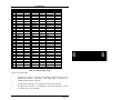
1
Artisan Technology Group is your source for quality
new and certified-used/pre-owned equipment
• FAST SHIPPING AND
DELIVERY
• TENS OF THOUSANDS OF
IN-STOCK ITEMS
• EQUIPMENT DEMOS
• HUNDREDS OF
MANUFACTURERS
SUPPORTED
• LEASING/MONTHLY
RENTALS
• ITAR CERTIFIED
SECURE ASSET SOLUTIONS
SERVICE CENTER REPAIRS
Experienced engineers and technicians on staff
at our full-service, in-house repair center
WE BUY USED EQUIPMENT
Sell your excess, underutilized, and idle used equipment
We also offer credit for buy-backs and trade-ins
www.artisantg.com/WeBuyEquipment
InstraView REMOTE INSPECTION
LOOKING FOR MORE INFORMATION?
Visit us on the web at www.artisantg.com for more
information on price quotations, drivers, technical
specifications, manuals, and documentation
SM
Remotely inspect equipment before purchasing with
our interactive website at www.instraview.com
Contact us: (888) 88-SOURCE | [email protected] | www.artisantg.com
®
EPC - 7
Hardware Reference
®
RadiSys Corporation
15025 S.W. Koll Parkway
Beaverton, OR 97006
Phone: (503) 646-1800
FAX: (503) 646-1850
______________________________________________________________________
07-0103-02
September 1994
Artisan Technology Group - Quality Instrumentation ... Guaranteed | (888) 88-SOURCE | www.artisantg.com
EPC-7 Hardware Reference
EPC and RadiSys are registered trademarks and EPConnect is a trademark of
RadiSys Corporation. OS/2, IBM, EGA, PS/2, and PC/AT are trademarks of
International Business Machines Corporation. 386 and 486 are trademarks of Intel
Corporation. Microsoft and MS-DOS are registered trademarks of Microsoft
Corporation.
February 1992
Copyright © 1992, 1994 by RadiSys Corporation
All rights reserved.
Page ii
Artisan Technology Group - Quality Instrumentation ... Guaranteed | (888) 88-SOURCE | www.artisantg.com
EPC-7 Hardware Reference
Hardware Warranty
RadiSys Corporation ("RadiSys") warrants the EPC system and component modules
to the original purchaser for two years from the product's shipping date. If an EPC
product fails to operate in compliance with its specification during this period,
RadiSys will, at its option, repair or replace the product at no charge. The customer
is, however, responsible for shipping the product; RadiSys assumes no responsibility
for the product until it is received. This warranty does not cover repair of products
that have been damaged by abuse, accident, disaster, misuse, or incorrect installation.
RadiSys' limited warranty covers products only as delivered. User modification, such
as the addition of memory arrays or other devices, may void the warranty, and if the
product is damaged during installation of the modifications, this warranty does not
cover repair or replacement.
This warranty in no way warrants suitability of the product for any specific
application.
IN NO EVENT WILL RADISYS BE LIABLE FOR ANY DAMAGES,
INCLUDING LOST PROFITS, LOST SAVINGS, OR OTHER INCIDENTAL OR
CONSEQUENTIAL DAMAGES ARISING OUT OF THE USE OR INABILITY
TO USE THE PRODUCT EVEN IF RADISYS HAS BEEN ADVISED OF THE
POSSIBILITY OF SUCH DAMAGES, OR FOR ANY CLAIM BY ANY PARTY
OTHER THAN THE PURCHASER.
THE ABOVE WARRANTY IS IN LIEU OF ANY AND ALL OTHER WARRANTIES, EXPRESSED OR IMPLIED OR STATUTORY, INCLUDING THE
WARRANTIES OF MERCHANTABILITY, FITNESS FOR A PARTICULAR
PURPOSE OR USE, TITLE AND NONINFRINGEMENT. Repair or replacement
as provided above shall be the Purchaser's sole and exclusive remedy and RadiSys'
exclusive liability for any breach of warranty.
Page iii
Artisan Technology Group - Quality Instrumentation ... Guaranteed | (888) 88-SOURCE | www.artisantg.com
EPC-7 Hardware Reference
NOTES
Page iv
Artisan Technology Group - Quality Instrumentation ... Guaranteed | (888) 88-SOURCE | www.artisantg.com
EPC-7 Hardware Reference
Contents
1. Product Description............................................................................................1
Specifications....................................................................................................2
2. Before Installation ..............................................................................................5
Configuring the EPC-7 Jumpers .......................................................................5
Slot 0 and System Controller Configuration ............................................5
Installing the VXIbus Backplane Jumpers........................................................7
3. Installation ..........................................................................................................11
EPC-7 Insertion.................................................................................................11
EXM Module Insertion .....................................................................................11
Connecting Peripherals to the EPC-7................................................................12
Monitor.....................................................................................................12
Keyboard ..................................................................................................12
Serial Port.................................................................................................13
Parallel Printer Port ..................................................................................13
SCSI Port..................................................................................................13
External Clock Input ................................................................................14
External Clock Output..............................................................................14
External Trigger .......................................................................................14
4. Configuring the BIOS Setup.............................................................................15
Power-On Screen Display.................................................................................15
BIOS Setup Screen ...........................................................................................16
EXM Configuration ..........................................................................................18
Fixed Disk Menu ..............................................................................................20
User-Definable Drive Types ....................................................................22
Disk Formatting ................................................................................................23
Low-level IDE (AT) Disk Formatting......................................................23
Page v
Artisan Technology Group - Quality Instrumentation ... Guaranteed | (888) 88-SOURCE | www.artisantg.com
EPC-7 Hardware Reference
5. Theory of Operation...........................................................................................25
Memory Map ....................................................................................................26
Processor and Memory .....................................................................................27
Cached and Uncached Addresses.............................................................27
ROM and ROM Shadowing..............................................................................27
SCSI Controller.................................................................................................28
Floppy Disk Controller .....................................................................................28
IDE Disk Interface ............................................................................................29
Battery...............................................................................................................29
Watchdog Timer ...............................................................................................30
EXM Expansion Interface.................................................................................31
VXIbus Interface...............................................................................................31
Slot 0 and System Controller Functions ...........................................................32
Reset Behavior ..................................................................................................32
Printed Circuit Board ........................................................................................34
6. Connectors ..........................................................................................................35
VXI Signal Usage .............................................................................................38
Floppy Connector .............................................................................................42
7. VXIbus Interface ................................................................................................43
Concepts............................................................................................................43
Memory Map............................................................................................43
Direct VMEbus Accesses .........................................................................44
Byte Ordering ...........................................................................................45
Slave Accesses from the VMEbus ...........................................................48
Self Accesses Across the VMEbus...........................................................48
Read-Modify-Write Operations ...............................................................49
VMEbus Interrupt Response ....................................................................50
Registers Specific to EPC-7..............................................................................50
Register State after Reset..........................................................................66
VXIbus Mapped Registers................................................................................67
Supported Address Modifiers ...........................................................................68
Low-Level Programming the VMEbus Interface .............................................68
VMEbus Accesses....................................................................................68
VXIbus Interrupt Handler .................................................................................71
Read-Modify-Write Operations ...............................................................74
Soft Reset and VME Sysreset ...........................................................................74
Page vi
Artisan Technology Group - Quality Instrumentation ... Guaranteed | (888) 88-SOURCE | www.artisantg.com
EPC-7 Hardware Reference
8. Upgrades..............................................................................................................77
Memory.............................................................................................................77
9. Troubleshooting & Error Messages..................................................................81
Troubleshooting ................................................................................................81
Common Error Messages..................................................................................84
SCSI related problems..............................................................................89
10. Support and Service ..........................................................................................91
Appendix A: Interrupts and DMA Channels........................................................A-1
Appendix B: I/O Map..............................................................................................B-1
Appendix C: Using the EPC-7 AM ........................................................................C-1
Index .........................................................................................................................I-1
Page vii
Artisan Technology Group - Quality Instrumentation ... Guaranteed | (888) 88-SOURCE | www.artisantg.com
EPC-7 Hardware Reference
Figures
Figure 1. EPC-7 Configuration Jumpers ................................................. 6
Figure 2. Daisy-Chain Signal Concept..................................................... 7
Figure 3. VXIbus Backplane Jumper Examples ...................................... 8
Figure 4. VXIbus Jumpers or DIP Switches on Front of Chassis ............ 9
Figure 5. VXIbus Jumpers on Rear Wirewrap Pins ..................................9
Figure 6. Power-on Screen Display.........................................................15
Figure 7. Main Setup Screen ...................................................................16
Figure 8. EXM Setup Screen...................................................................19
Figure 9. EXM Slot Numbering..............................................................19
Figure 10. Fixed Disk Menu ...................................................................21
Figure 11. Location of Disk Drive Label ................................................22
Figure 12. Data Path Block Diagram ......................................................25
Figure 13. EPC Battery Location ............................................................29
Figure 14. Battery Removal ....................................................................30
Figure 15. PCB Layout ...........................................................................34
Figure 16. Little-Endian Byte Order .......................................................46
Figure 17. Big-Endian Byte Order ..........................................................47
Figure 18. Location of SIMM Sockets....................................................79
Tables
Table 1. EPC-7 Environmental Specs With No Internal Disk Drives.......2
Table 2. EPC-7 Environmental Specs With Floppy and Hard Drives ......3
Table 3. Additional EPC-7 Specifications ................................................4
Table 4. Fixed Disk Configuration Example...........................................23
Table 5. Physical Address Space Mapping .............................................26
Table 6. DB-9 Pinout ..............................................................................35
Table 7. COM2 10-Pin Header Pinout ....................................................35
Table 8. DB-25 LPT1 Pinout ..................................................................36
Table 9. Keyboard Connector Pinout......................................................36
Table 10. SCSI Port Pinout .....................................................................37
Table 11. Speaker Header Pinout............................................................38
Table 12. VXIbus Signal Usage..............................................................39
Table 13. VXIbus P2 Connector .............................................................40
Table 14. P1 Connector Pinout ...............................................................41
Table 15. 34-Pin and 26-Pin Floppy Connector Pin-outs .......................42
Table 16. A16 Register Mapping ............................................................67
Table 17. Supported Address Modifiers .................................................68
Table 18. Interrupt Assignments ............................................................A1
Table 19. DMA Channels.......................................................................A2
Table 20. I/O Map ..................................................................................B5
Page viii
Artisan Technology Group - Quality Instrumentation ... Guaranteed | (888) 88-SOURCE | www.artisantg.com
1
1. Product Description
This manual contains all the information needed to install and use the EPC-7 VXIbus
embedded computer. Additional user and programmer manuals discuss the use of the
EPConnect software package designed to work with the EPC-7.
The EPC-7 is a C-size VXIbus embedded computer based on the Intel 486 processor.
It can perform 8-, 16-, and 32-bit VXIbus data transfers, both as master and slave,
and can be the slot-0 and system controller and resource manager. The EPC-7 can be
an interrupter and interrupt handler, and can drive and sample the TTL and ECL
trigger lines.
The EPC-7 is compatible with the IBM PC architecture and contains standard frontpanel connectors for PC serial and parallel ports. The keyboard port is PS/2 style. In
addition, the front panel contains a SCSI-2 port and cable connectors for external
clock and trigger signals.
Depending on the model, the EPC-7 contains three or four front-panel expansion slots
for EXM modules. Also, the particular model of the EPC-7 will determine such
attributes as the speed of the 486 processor, the size of the internal hard disk, the
amount of the DRAM memory, and whether a floppy diskette drive is present.
Page 1
Artisan Technology Group - Quality Instrumentation ... Guaranteed | (888) 88-SOURCE | www.artisantg.com
1
EPC-7 Hardware Reference
1
1
Specifications
The following tables define the power and environmental specifications of the
EPC-7. They do not include any EXM modules in the EPC-7.
The following are the environmental specifications of the EPC-7 when it contains no
internal disk drives.
Characteristic
Environmentals
Temperature
operating
storage
Cooling
Humidity
Altitude
Vibration
operating
storage
operating
storage
operating
storage
Shock
operating
storage
Value
0°C - 60°C at point of entry of forced air
derated 2°C per 1000 ft (300 m) over 10,000
ft (3,000m)
2°C per min max excursion gradient
-40 - 85°C
5°C per min max excursion gradient
For 10°C rise, airflow of 2 liters per second
against 0.014mm H2O backpressure
5% - 95% noncondensing
5% - 95% noncondensing
0 - 10,000 ft (3000 m)
0 - 40,000 ft (12,000 m)
0.015 inch (0.38 mm) P-P displacement with
2.5 g peak (max) acceleration over
5-2000 Hz
0.030 inch (0.76 mm) P-P displacement with
5.0 g peak (max) acceleration over
5-2000 Hz
30 g, 11 ms duration, half-sine shock pulse
50 g, 11 ms duration, half-sine shock pulse
Table 1. EPC-7 Environmental Specifications With No Internal Disk Drives.
Page 2
Artisan Technology Group - Quality Instrumentation ... Guaranteed | (888) 88-SOURCE | www.artisantg.com
Product Description
The following are the environmental specifications of the EPC-7 when it contains
floppy and hard disk drives.
Characteristic
Temperature
operating
storage
Cooling
Humidity
operating
storage
Altitude
Vibration
operating
storage
operating
storage
Shock
operating
storage
1
Value
5°C - 45°C at point of entry of forced air
derated 2°C per 1000 ft (300 m) over 10,000
ft (3000m)
10°C per hour max excursion gradient
-40°C - 70°C
2°C per hour max excursion gradient
For 10°C rise, airflow of 2 liters per second
against 0.014mm H2O backpressure
20% - 80% noncondensing
26°C max wet bulb
5% - 95% noncondensing
48°C max wet bulb
0 - 10,000 ft (3000 m)
0 - 40,000 ft (12,000 m)
0.015 inch (0.38 mm) P-P displacement with
0.6 g peak (max) acceleration over
5-500 Hz
0.030 inch (0.76 mm) P-P displacement with
2.0 g peak (max) acceleration over
5-500 Hz
5 g, 11 ms duration, half-sine shock pulse,
no soft errors, 10 g with 1 soft error per
block
10 g, 11 ms duration, half-sine shock pulse
Table 2. EPC-7 Environmental Specifications With Floppy and Hard Drives.
Page 3
Artisan Technology Group - Quality Instrumentation ... Guaranteed | (888) 88-SOURCE | www.artisantg.com
1
EPC-7 Hardware Reference
1
1
The following table contains additional specifications.
measured with hard and floppy drives and no EXMs.
Characteristic
Electrical
Current
+5V
+12V
-12V
-5.2V
-2V
Other
Weight
VME
VXI
without EXMs
master address
master transfer
slave address
slave transfer
interrupter
interrupt handler
requester
arbiter
system controller
device type
protocols
manufacturer
code
model code
Power and current are
Value
6.0 A typ, 7.0 A max (33 MHz)
7.0 A typ, 8.0 A max (50 MHz)
7.5 A typ, 8.5 A max (100 MHz)
1.1 A max for first 10 sec after power on for
hard-drive spin up, 0.5 A max thereafter
0.1 A max
0.3 A max
0.12 A max
5.5 lb (2.6 kg)
A16, A24, A32
D08(EO), D16, D32, RMW
A16, A24, A32
D08(EO), D16, D32, RMW
I(1-7)
D08(O),D16 IH(1-7)
ROR,RONR
RRS,PRI
SYSCLK, IACK daisy chain, bus timer
message based
cmdr/master/interrupter
4076 - RadiSys Corporation
239 (if configured for slot 0)
495 (if configured for not slot 0)
Table 3. Additional EPC-7 Specifications.
Page 4
Artisan Technology Group - Quality Instrumentation ... Guaranteed | (888) 88-SOURCE | www.artisantg.com
2. Before Installation
2
Before installing the EPC-7, unpack and inspect it for shipping damage.
DO NOT REMOVE ANY MODULES FROM THEIR ANTI-STATIC BAGS
UNLESS YOU ARE IN A STATIC-FREE ENVIRONMENT. THE EPC-7
MODULES, LIKE MOST OTHER ELECTRONIC DEVICES, ARE
SUSCEPTIBLE TO ESD DAMAGE.
ESD DAMAGE IS NOT ALWAYS
IMMEDIATELY OBVIOUS, IN THAT IT CAN CAUSE A PARTIAL
BREAKDOWN IN SEMICONDUCTOR DEVICES THAT MIGHT NOT
IMMEDIATELY RESULT IN A FAILURE.
THE EPC-7 CONTAINS A HARD DISK.
PLEASE HANDLE IT WITH
CARE.
Configuring the EPC-7 Jumpers
Slot 0 and System Controller Configuration
Before installing the EPC-7 in a VXIbus chassis, a decision must be made whether
the EPC-7 is to be the slot 0 controller and the VMEbus system controller. Every
VXIbus system needs a module that performs the VMEbus system controller
functions (generation of the 16 MHz SYSCLK signal, arbitration of the bus, detection
of bus timeout conditions, and initiation of the interrupt-acknowledge daisy chain),
and the VXIbus slot-0 functions (generation of the 10 MHz ECL CLK10 signals and
control of the MODID module identification function).
Typically, the same device is the slot-0 controller and VMEbus system controller.
The EPC-7 is shipped configured as a VXI slot 0 controller. If this is the intended
use of the EPC-7 (which will usually be the case), skip the rest of this section.
The EPC-7 has nine jumper positions appearing through its rear panel between the
P1 and P2 connectors. See Figure 1 below.
Page 5
Artisan Technology Group - Quality Instrumentation ... Guaranteed | (888) 88-SOURCE | www.artisantg.com
2
EPC-7 Hardware Reference
EPC-7 Rear View
2
2
Jumpers
E P C- 7 is s lot- 0 c ontr oller
E PC- 7 is not the slot- 0 c ontroller
Figure 1. EPC-7 Configuration Jumpers.
There are several readily apparent consequences of incorrectly configuring the
EPC-7 configuration jumpers.
−
−
−
−
−
−
Resource manager reports a system configuration differing widely from the
actual configuration
Power-on selftest reports a VXI failure.
CLK10+ and CLK10- signals are not being driven or are out of spec on the
backplane.
The system resource manager could not detect the presence of a non-slot-0
EPC-7.
Power-on selftest reports NO SYSCLK.
System hangs, typically while running the resource manager.
If any of these conditions occur, check the configuration jumpers on the back of the
EPC-7.
Page 6
Artisan Technology Group - Quality Instrumentation ... Guaranteed | (888) 88-SOURCE | www.artisantg.com
Before Installation
Installing the VXIbus Backplane Jumpers
The VXIbus contains several daisy-chained control signals. Most VXIbus
backplanes contain jumpers or DIP switches for these control signals to allow
systems to operate across empty slots. Failing to install these jumpers properly is a
common source of problems when integrating a new VXIbus system. In this manual,
these jumpers or DIP switches will be referred to as jumpers.
2
The VXIbus specification provides 4 bus grant signals (BG0 - BG3) and 1 interrupt
acknowledge signal (IACK) via daisy-chain lines. Per the VXIbus specifications, all
boards are required to correctly handle these signals. All slots that do not have a
board plugged into the backplane (i.e. empty slots and slots occupied by some multislot instruments), need to be jumpered to allow the signals to pass through to other
instruments in the system.
xxxIN
xxxIN
xxxIN
xxxIN
xxxOUT
xxxOUT
xxxOUT
xxxOUT
VXIbus Slots
Figure 2. Daisy-Chain Signal Concept.
The Slot-0 controller board initiates each daisy-chain signal. Each VXIbus slot to the
right of the Slot-0 controller must pass through each of the daisy-chain signals. For
each VXIbus slot, xxxIn pin must be connected to its corresponding xxxOut pin
(e.g. BG0In to BG0Out, BG1In to BG1Out,...,IackIn to IackOut) either
through the board in that slot or by jumpers.
Some boards correctly pass all of these signals, some boards handle some of these
signals and not others, and some boards (typically "dumb" slave boards) may not
Page 7
Artisan Technology Group - Quality Instrumentation ... Guaranteed | (888) 88-SOURCE | www.artisantg.com
2
EPC-7 Hardware Reference
handle any of these signals. Check the manual for each board to be installed to
determine if these signals are passed through correctly. If they are not or if the
VXIbus slot is empty, all (or some) of these signals must be jumpered. See Figure 3
below.
2
2
indicates jumper needed
BG0
BG1
BG2
BG3
IACK
Single Board Computer
that only handles
IACK & BG3
"Dumb" Slave
Does not handle
any of the signals
Figure 3. VXIbus Backplane Jumper Examples.
Page 8
Artisan Technology Group - Quality Instrumentation ... Guaranteed | (888) 88-SOURCE | www.artisantg.com
Before Installation
Now that you have determined where the jumpers need to be, you must determine
how to jumper your particular backplane. VXIbus chassis provide jumper
connections in one of three ways; stake pins, DIP switches, or auto jumpering. If the
chassis in use auto-jumpers the daisy-chain signals, proceed to the next chapter.
Different backplane manufacturers handle jumpers and DIP switches in different
ways; some provide stake pins on the rear of the backplane while others provide stake
pins or DIP switches on the front of the backplane. These stake pins can be located
in several different places.
2
If the stake pins are on the rear of the backplane, the most common place is in the
middle of the J1 connector as shown in Figure 5 below. This can be just these pins
extended or all pins extended for wirewrapping.
Page 9
Artisan Technology Group - Quality Instrumentation ... Guaranteed | (888) 88-SOURCE | www.artisantg.com
2
EPC-7 Hardware Reference
J1 Connectors
The stake pins (front or rear) can also be located adjacent to the slot
being jumpered as shown in Figure 4 above. Typically, the stake pins
will be located between the slot being jumpered and the next lowernumbered slot (e.g. jumpers for Slot 6 would be located adjacent to Slot
6 between Slots 5 and 6).
J1 Connector
BG0
BG1
BG2
2
2
BG3
BG0
BG1
BG2
BG3
Consult your VXI chassis reference manual or contact the chassis
manufacturer if you are unsure where to jumper your particular system.
IACK
The EPC-7 occupies two VXI slots and correctly handles all bus grant
and IACK signals for both slots. No jumpers are needed for these two
slots. If an EPC-7AM or EPC-7MC is also being used, it occupies a third
VXI slot. Jumpers must be installed for this slot.
IAC
Figure 4. VXIbus Jumpers or
DIP Switches
on Front of Chassis.
Figure 5. VXIbus Jumpers
on Rear Wirewrap Pins.
Page 10
Artisan Technology Group - Quality Instrumentation ... Guaranteed | (888) 88-SOURCE | www.artisantg.com
Before Installation
NOTES
2
Page 11
Artisan Technology Group - Quality Instrumentation ... Guaranteed | (888) 88-SOURCE | www.artisantg.com
2
3. Installation
3
EPC-7 Insertion
The EPC-7 is inserted in a VXIbus card cage in the following way:
1.
Make sure that power to the VXI system is off. The modules are not
designed to be inserted or removed from live backplanes.
2.
Align the EPC-7 to adjacent top and bottom card guides in the VXI
chassis.
3.
Slide the EPC-7 module into the chassis. Use firm pressure on the
handles to mate the module with the backplane connectors.
4.
Tighten the screws in the top and bottom of the front panel to ensure
proper connector mating and prevent loosening of the module via
vibration.
Note that the EPC-7 has a front-panel key adhering to the VXIbus specification that
prevents its insertion to the right of certain other types of modules. These keys
prevent problems associated with incompatible signal levels on the VXI daisychained Local Bus. Although the EPC-7 does not use the Local Bus, its ability to be
a slot-0 controller means that it uses what would otherwise be "leftside" Local Bus
lines for TTL MODID lines. Therefore the key prevents the EPC-7 from being
installed to the immediate right of a module keyed for a "rightside" ECL, analog, or
sensor Local Bus.
EXM Module Insertion
Your EPC-7 will typically have several EXM expansion modules for such purposes
as a video controller, network interface, and GPIB interface. If an EXM needs to be
removed or replaced, loosen the two thumbscrews on the EXM and gently pull it out
of its rear connector.
Page 11
Artisan Technology Group - Quality Instrumentation ... Guaranteed | (888) 88-SOURCE | www.artisantg.com
3
EPC-7 Hardware Reference
To insert an EXM, slide the EXM into place in the card guides, push firmly on the
EXM front panel to seat the rear cardedge connector, and tighten the thumb screws
on the EXM's face plate.
MAKE SURE THAT POWER TO YOUR VXI SYSTEM IS OFF. EXMS ARE
NOT DESIGNED TO BE INSERTED OR REMOVED FROM LIVE
SYSTEMS.
3
3
WHEN INSERTING AN EXM, AVOID TOUCHING THE CIRCUIT BOARD,
AND MAKE SURE THE ENVIRONMENT IS STATIC-FREE.
Connecting Peripherals to the EPC-7
The final step of installation is connecting peripherals, typically a video display and
keyboard, but also perhaps a mouse, modem, printer, etc. Unless otherwise noted, all
connectors are compatible with those found on IBM-compatible desktop PCs.
Detailed pin assignments are described in Chapter 6.
Monitor
The EPC-7 contains no built-in connection for a monitor. Typically the EPC-7
contains an EXM-13A video controller for connection to an analog VGA monitor.
Use of the EXM-13A is summarized below. Consult the EXM-13A reference manual
for further details.
Monitors that can be used with the EXM-13A are VGA-compatible monitors (i.e.,
those compatible with the IBM PS/2 and with PC VGA add-in cards) and multiscan
(multifrequency or "multisync") monitors. Refer to the EXM-13A manual for more
information. If you cannot mate your monitor to the 15-pin connector on the EXM
because you have a cable with a 9-pin connector, either (1) you have a TTL monitor
that is not compatible with VGA or (2) you have a multisync monitor (which are
usually shipped with 9- and 15-pin cables or adapters) and are using the wrong cable.
If using a multiscan monitor, make sure to set the monitor's switch to analog (not
TTL).
Keyboard
The front panel contains a keyboard connector compatible with that of the IBM PS/2.
An adapter cable is provided so that keyboards with the larger five-pin PC/AT
connectors can be used.
Page 12
Artisan Technology Group - Quality Instrumentation ... Guaranteed | (888) 88-SOURCE | www.artisantg.com
Installation
If the BIOS produces the message "KEYBOARD ERROR OR NO KEYBOARD
PRESENT" at time of power-on or reset, either no keyboard is present, the keyboard
cable is not firmly connected, a key was pressed, or the keyboard is not a PC/AT
compatible keyboard.
If you wish to operate your system without a keyboard, you must start with a
keyboard and invoke the BIOS setup screen to change the Configuration Errors field
to "ignore keyboard errors."
3
Serial Port
The front panel contains one DB-9 serial-port connector. It is identical to the serial
port labeled COM1 in the PC/AT and compatibles. It may be used for connecting a
mouse, modem, serial printer, RS-232 link, etc.
If your EPC-7 contains a conductive plastic ESD shield on the connector, remove it
only when connecting a device. Leaving it on the connector when the connector is
not being used will reduce the possibility of ESD (electrostatic discharge) damage
through the connector.
Parallel Printer Port
The parallel port on the front panel is compatible with the corresponding DB-25
LPT1 connector on IBM PCs and compatibles. Typically it is used to connect
printers and software security keys.
SCSI Port
The SCSI connector is a high-density, 50-pin, standard SCSI-2 connector. The
connector type is "shielded alternative 1" in the SCSI-2 specification. This connector
is an AMP 174726-4 (or equivalent) socket. This SCSI implementation uses the
Adaptec AIC 6360 chip and is therefore compatible with the Adaptec AHA
1520/1522 PC add-in card.
Drivers are available for a range of operating systems and SCSI devices, including
disks, streaming tapes, CD-ROMs, and digital audio tapes. These drivers do not ship
with the product; contact RadiSys for more information.
Page 13
Artisan Technology Group - Quality Instrumentation ... Guaranteed | (888) 88-SOURCE | www.artisantg.com
3
EPC-7 Hardware Reference
External Clock Input
3
3
The EPC-7 provides the option, when it is configured as the slot-0 controller, of
deriving the ECL CLK10 signal from an internal oscillator or from a 10 MHz
external clock source. An SMB connector is provided on the front panel. The
external clock input is TTL compatible. It is not resistively terminated. It presents one
FAST TTL unit load (IIH < 0.02mA, IIL < -0.6 mA). The external clock signal must
have TTL levels. The choice of clock source is specified in the clock control register,
8162. Refer to Chapter 7, VXIbus Interface, for more information.
External Clock Output
A second SMB connector provides a TTL form of the CLK10 clock. It can drive a
50 ohm line. This is typically used to synchronize multiple VXI mainframes.
External Trigger
A third SMB connector provides for an external TTL trigger signal input or output.
When configured as an input, it is not resistively terminated and presents one FAST
TTL unit load (IIH < 0.02mA, IIL < -0.6 mA). When configured as an output, it can
drive a 50 ohm line. The direction of the signal and the association to a specific
backplane trigger line is controlled by the external trigger register, 8163. Refer to
Chapter 7, VXIbus Interface, for more information.
Page 14
Artisan Technology Group - Quality Instrumentation ... Guaranteed | (888) 88-SOURCE | www.artisantg.com
4. Configuring the
BIOS Setup
Power-On Screen Display
Whenever a hardware reset (power-on or front-panel) occurs on the EPC-7,
information is displayed on the attached monitor showing the status of the BIOS
selftest and the amount of memory found. If everything proceeds normally, the
screen image should appear approximately as shown in the following figure.
4
486 Modular BIOS version 3.05abd,
Copyright (c) 1984-90 Award Software Inc.
Copyright 1991 RadiSys Corporation
BIOS V3.05
TESTING INTERRUPT CONTROLLER #1........................................OK
TESTING INTERRUPT CONTROLLER #2........................................OK
TESTING CMOS BATTERY...................................................OK
TESTING CMOS CHECKSUM..................................................OK
TESTING VME INTERFACE..................................................OK
TESTING VXI INTERFACE..................................................OK
SIZING SYSTEM MEMORY............................................640K
FOUND
TESTING SYSTEM MEMORY...........................................640K
OK
CHECKING UNEXPECTED INTERRUPTS AND STUCK NMI...........................OK
TESTING PROTECTED MODE.................................................OK
SIZING EXPANSION MEMORY.........................................7168K
FOUND
TESTING MEMORY IN PROTECTED MODE................................7808K
FOUND
TESTING PROCESSOR EXCEPTION INTERRUPTS.................................OK
TESTING SERIAL PORT #1.................................................OK
TESTING SERIAL PORT #2.................................................OK
TESTING PARALLEL PORT..................................................OK
Figure 6. Power-on Screen Display.
Page 15
Artisan Technology Group - Quality Instrumentation ... Guaranteed | (888) 88-SOURCE | www.artisantg.com
4
EPC-7 Hardware Reference
Some error messages might occur during the execution of the BIOS
initialization sequence. If errors occur during the power-on self-test (POST), the
BIOS will display the error on the appropriate line of the screen display and attempt
to continue.
BIOS Setup Screen
The EPC-7's BIOS contains a setup function to display and alter the system
configuration. This information is maintained in the EPC-7's nonvolatile CMOS
RAM and is used by the BIOS to initialize the EPC-7 hardware.
4
4
To invoke the setup function in a "booted" system, press the CTRL+ALT+ESC keys
simultaneously. This may be done during system operation in most, but not all circumstances. Some programs that take control of the keyboard at a low level, such as
Microsoft Windows, cause this key sequence to be interpreted differently, or not at
all. It should always work, however, when the DOS operating system prompt is
shown on the screen. The setup function can be invoked prior to system booting by
pressing CTRL+ALT+ESC immediately after the initial selftest screen is cleared.
The main setup screen will be similar to the following.
RadiSys EPC-7 CMOS Setup, System BIOS V3.05
50MHz 486, 16 MBytes memory
Date (mm/dd/yy) .............. ... 12/02/93
Time (hh:mm:ss) .............. ... 07:34:56
Configuration Errors ......... ... Halt on all errors
Diskette Drive A ............. ... 1.4M
Fixed Disk Drive C .......... AT
Fixed Disk Drive D .......... None
Bus Priority .................
Bus Release Method ...........
Bus Arbitration ..............
COM1: ........................
COM2: ........................
LPT1: ........................
...
...
...
...
...
...
3.5 inch
Pri 3
RONR
Priority
Enabled
Disabled
Enabled
F2 =
F3 =
F10 =
ESC =
EXM menu
Fixed disk menu
Save CMOS and EXM data
Exit without saving
Figure 7. Main Setup Screen.
Page 16
Artisan Technology Group - Quality Instrumentation ... Guaranteed | (888) 88-SOURCE | www.artisantg.com
Configuring the BIOS Setup
Use the up and down cursor (arrow) keys to move from field to field. For most
fields, position the cursor at the field and press the left and right cursor (arrow) keys
to rotate through the available choices. Once the screen has been changed to appear
as desired, press the F10 function key to save the changes in nonvolatile (batterybacked) CMOS RAM and then press the F5 function key to confirm the changes and
reboot. Alternately, press the ESC key to ignore any changes and exit.
The fields are explained below.
DATE and TIME
These values are changed by moving to this field and typing in the format shown.
CONFIGURATION ERRORS
This field gives you several choices about the situations under which the BIOS
should wait for user input if a configuration error is found. The selections are
4
1) halt on all errors,
2) ignore all errors,
3) ignore keyboard errors
(allows operation without a keyboard),
4) ignore disk errors, and
5) ignore keyboard and disk errors.
DISKETTE DRIVE
This field identifies the type of floppy disk drive installed as the A drive. If the
EPC-7 has a floppy drive installed, the proper setting is for a 3.5" 1.44 MB floppy
disk drive. If no drive is installed, the proper setting is NONE.
FIXED DISK DRIVE
This display-only field shows the type of disk selected from the fixed disk menu. To
see the detailed characteristics of the device or to change the device, use the F3
function key to go to the fixed disk menu.
BUS PRIORITY
This field allows selection among the four VXIbus priority levels. This is the level at
which the EPC-7 will contend for the bus when it performs a VXIbus access.
Page 17
Artisan Technology Group - Quality Instrumentation ... Guaranteed | (888) 88-SOURCE | www.artisantg.com
4
EPC-7 Hardware Reference
BUS RELEASE METHOD
This field entry toggles between two bus release modes: ROR (release on request)
and RONR (request on no request, also known as the VXI fair-requester mode).
ROR results in slightly better EPC-7 performance when accessing the VXIbus;
RONR directs the EPC-7 to not "park" on the bus and thus slightly improves the
access time of other VXIbus masters to the bus. When using RONR, all masters on
the VXIbus should be set to RONR to avoid a starvation condition where one master
never gains access to the bus.
BUS ARBITRATION
4
4
This field toggles between the two arbitration algorithms provided by the EPC-7:
priority arbitration and round-robin arbitration. This field is only used when the
EPC-7 is configured as the slot-0 controller:
COM1, COM2, LPT1
These fields toggle between the enabled and disabled states. The enabled state
enables the controllers for these I/O ports. The disabled state means that the
associated I/O port is disabled, and the I/O addresses and IRQs associated with the
controller for the port are not responded to by the controller. Putting a port in the
disabled state allows use of I/O modules that may have conflicting addresses or IRQs
with the built-in ports.
EXM Configuration
A separate EXM setup screen is used to configure the EXM modules in the system. It
is displayed by pressing the F2 function key from the main setup screen. The
EPC-7's nonvolatile (battery-backed) CMOS holds identification and configuration
information for up to six EXM module slots. Note that six EXM slots are indicated
even in systems that do not have six EXM slots available. An EPC-7MC module
carrier can be added to a standard EPC-7 to provide two additional EXM slots. This
is a factory-installed option only.
Page 18
Artisan Technology Group - Quality Instrumentation ... Guaranteed | (888) 88-SOURCE | www.artisantg.com
Configuring the BIOS Setup
The BIOS displays the configuration information in hexadecimal format.
RadiSys EPC-7 EXM Setup, System BIOS V3.05
50MHz 486, 16 MBytes memory
Slot
0
1
2
3
4
5
ID
FF
FF
FF
FF
FF
FF
OB1
00
00
00
00
00
00
OB2
00
00
00
00
00
00
F10 = Okay
ESC = Cancel
Figure 8. EXM Setup Menu.
EXMs must be defined in this screen so the BIOS can correctly identify and initialize
each one at boot-up. Each EXM must be listed by slot number, ID and two option
bytes as defined below.
SLOT
4
indicates the EXM slot in which the EXM is installed. See
the figure below to determine which slot each EXM occupies. Note
that, when installed, the floppy disk drive occupies EXM
slot 0. Dotted lines indicate EXM slot numbers for an optional
EPC-7MC module carrier.
C 1 3 5
P
U
0 2 4
Figure 9. EXM Slot Numbering.
ID
is a hard-wired ID value. Each type of EXM has a unique ID value.
OB1/OB2
are two "option" bytes of configuration information.
All slots not occupied by an EXM module should show an ID of FF and OB1/OB2 of
00 00 indicating that no EXM is present. This includes slot 0 if the floppy drive is
installed.
Page 19
Artisan Technology Group - Quality Instrumentation ... Guaranteed | (888) 88-SOURCE | www.artisantg.com
4
EPC-7 Hardware Reference
Consult the EXM manual for the correct configuration information for each EXM
expansion module installed.
After all EXMs have been configured, press F10 to save the data or ESC to ignore the
changes. In either case you will be returned to the main setup screen.
When using EXMs with configurable interrupts, DMA channels, I/O addresses,
and/or memory addresses, avoid conflicts with built-in functions of the EPC-7.
Guidelines are:
1.
4
4
2.
3.
4.
If an interrupt is needed, use IRQ3, IRQ5, IRQ9, IRQ12, or IRQ15.
IRQ7 can be used if the printer port is not being used. IRQ3 should not
be used if the COM2 port is being used. COM2 is available on the
EPC-7AM adapter module. (Refer to Appendix C for installation
information concerning the EPC7-AM.)
Use DMA channels 1, 3, 6, and 7. Channels 0 and 5 may also be used,
depending on whether you are using the SCSI interface and how it is
configured.
Do not select I/O addresses that conflict with those in the EPC-7. A
complete list appears in Appendix B. For instance, I/O addresses in the
300-33F range can be used.
If the EXM needs to use upper memory addresses, they must be in the
0D0000-0DFFFF range.
Fixed Disk Menu
The Fixed Disk Menu is used to define the type of hard disk(s) installed in the
system. Enter the Fixed Disk Menu screen by pressing the F3 function key from the
main setup screen.
Page 20
Artisan Technology Group - Quality Instrumentation ... Guaranteed | (888) 88-SOURCE | www.artisantg.com
Configuring the BIOS Setup
The Fixed Disk Menu screen looks similar to the one below.
RadiSys EPC-7 Fixed Disk Menu, System BIOS V3.05
50MHz, 16 MBytes memory
Fixed Disk Drive C: AT
Type 40
101 MBytes:
Landing Zone: 1023
754 Cyls, 16 Heads, 17 Sectors
Precompensation: None
Fixed Disk Drive D: None
F10
ESC
= Save and return
= Return without saving
Figure 10. Fixed Disk Menu.
AT
Disk type AT denotes the many types of non-SCSI PC/AT
compatible drives including IDE. Scroll through the numeric drive
types listed to find the one matching the characteristics of the hard
drive as shown on the drive sticker located on the right side panel
of the EPC-7. If no pre-defined drive type matches the installed
drive, use the user-definable drive types 48 or 49.
None
Choose None if there is no hard disk present.
SCSI
Choose SCSI to activate the built-in SCSI BIOS. Use this option
only if you are not using a loadable device driver (such as those
included with the EZ-SCSI software). There are no fixed disk
characteristics to select because the BIOS determines them
dynamically. If Drive C is set to SCSI, Drive D must also be set to
SCSI even if no second drive is installed. If this is not done, the
system will prompt you to correct the problem before exiting this
screen.
EXM Flash
Choosing disk type EXM Flash tells the BIOS to use a flash
memory device (e.g., EXM-2A) as a drive. An EXM-2A can be
made the boot device by making EXM Flash the drive C type.
However, if Drive C is EXM Flash, Drive D must be set to None.
4
Page 21
Artisan Technology Group - Quality Instrumentation ... Guaranteed | (888) 88-SOURCE | www.artisantg.com
4
EPC-7 Hardware Reference
P1
Drive Label
P2
4
4
Figure 11. Location of Disk Drive Label.
User-Definable Drive Types
If the correct AT disk type is not listed, the EPC-7 provides user-editable drive types
48 and 49. Select either of these drive types. Use the TAB key (→| )or the left and
right cursor keys (← →) to move to the next (or previous) field. Note that the default
settings for MBytes, Cylinders, Heads, and Sectors is 1. MBytes is a display-only
field calculated by the BIOS. Move the cursor to each field (Cyls, Heads, and
Sectors) and type the value for that field.
If a drive label exists on the right side panel (refer to Figure 11), use the parameters
listed on the label.
When installing a user-supplied replacement IDE hard disk, consult the hard disk
manual for the correct values to use for cylinders, heads and sectors. The BIOS
allows use of the following maximum values:
Cylinders
1023
Heads
63
Page 22
Artisan Technology Group - Quality Instrumentation ... Guaranteed | (888) 88-SOURCE | www.artisantg.com
Sectors
16
Configuring the BIOS Setup
The new hard disk may have parameters larger than the allowable maximum. If the
drive parameters are greater than the allowable maximum, divide the actual number
of cylinders by 2 and multiply the actual number of heads by 2. IDE drives use
Universal translation mode. That is, each sector is addressed as an absolute sequential
sector number. Since the embedded "intelligent" controller converts the sector data to
an absolute number, these "false" cylinder and head numbers will still allow the drive
to be used. The example on the next page shows how this is done.
Example:
Cylinders
Heads
Sectors
Total
Sectors
Actual
parameters
1350
5
32
Conversion
factor
divide by 2
multiply by
2
(none)
216,000
Numbers
to Use
675
4
10
32
216,000
Table 4. Fixed Disk Configuration Example.
After the Fixed disk(s) have been configured, press F10 to save the data or ESC to
ignore the changes. In either case you will be returned to the main setup screen.
Disk Formatting
The hard disk in the EPC-7 is an IDE disk which is "hard sectored"; therefore it does
not require low-level formatting. Depending on the context in which you ordered the
EPC-7, the disk is either bootable (containing an operating system and other software
pre-installed) or empty (neither partitioned nor formatted).
Low-level IDE (AT) Disk Formatting
Low-level formatting was originally performed on "soft-sectored" hard disks to
establish logical sectors, map out bad sectors, create the master boot block, etc. Since
IDE hard disks are "hard-sectored", they do not need low-level formatting. However,
the original purpose of low-level formatting has evolved and it is now also used to
wipe a disk clean of all data.
Page 23
Artisan Technology Group - Quality Instrumentation ... Guaranteed | (888) 88-SOURCE | www.artisantg.com
4
EPC-7 Hardware Reference
For low-level formatting of an IDE hard drive, a disk utility must be used, such as
DOSUTILS from Ontrack Computer Systems, Inc., QAPlus from DiagSoft, Inc.,
AMIDIAG from American Megatrends Inc., or SuperSoft Service Diagnostics from
SuperSoft Inc. Low-level formatting is rarely necessary and in fact, is not possible on
some of the new higher capacity IDE drives.
4
4
Page 24
Artisan Technology Group - Quality Instrumentation ... Guaranteed | (888) 88-SOURCE | www.artisantg.com
5. Theory of Operation
This chapter specifies other information about the operation of the EPC-7 that might
be useful to the system designer. The block diagram below shows the overall datapath structure of the EPC-7. Note that numbers in parentheses denote the data width
of the path.
486
SCSI
controller
Floppy
disk
controller
(32)
(16)
RadiSys datapath switch
gate array
(pair)
(8)
(64)
(32)
VXI
VXIbus
bus
(8)
5
(16)
VXI gate
arrays and
control logic
DRAM
IDE
disk
interface
ATU ASIC
(DMA, interrupt ctrl,
clock, timers,
control, reset logic)
EXM
Expansion
Interface
(16)
Reset switch
BIOS
Serial and
parallel port
controller
Battery
Speaker
8242
keyboard
controller
Figure 12. Data Path Block Diagram.
Page 25
Artisan Technology Group - Quality Instrumentation ... Guaranteed | (888) 88-SOURCE | www.artisantg.com
5
EPC-7 Hardware Reference
Memory Map
32
The 2 byte physical address space seen by the CPU is mapped according to the
following table.
Range
00000000 0009FFFF
000A0000 000BFFFF
5
5
Content
DRAM
Uncommitted, mapped to EXM expansion interface
(typically, with a VGA video controller EXM installed,
0A0000-0BFFFF will be the video RAM and 0C00000C7FFFF will be the video BIOS)
000C0000 000CFFFF DRAM (see bit MDCF in memory mode register)
000D0000 000DFFFF Uncommitted, mapped to EXM expansion interface
000E0000 000EFFFF Mappable window onto VXI data transfer bus or
uncommitted, mapped to EXM expansion interface,
controlled by bit in register 8102h
000F0000 000FFFFF DRAM (used for BIOS shadowing)
Write-protected.
00100000 00FDFFFF DRAM or EXM expansion interface (to DRAM to the
extent of the value of MEMS in the memory mode
register)
00FE0000 00FFFFFF
Mapped to BIOS ROM or DRAM (see bit MDFF in
memory mode register)
01000000 03FFFFFF DRAM or EXM expansion interface (see bit MEMS in
the memory mode register)
04000000 0FFFFFFF Mapped to EXM expansion interface
10000000 EFFFFFFF Mapped to VXIbus
F0000000 FFFFFFFF Mapped to EXM expansion interface. On the EXM
expansion interface, ranges xxFExxxx and xxFFxxxx are
ROM.
Table 5. Physical Address Space Mapping.
Little-endian and big-endian byte ordering is discussed in Chapter 7, VXIbus
Interface.
Page 26
Artisan Technology Group - Quality Instrumentation ... Guaranteed | (888) 88-SOURCE | www.artisantg.com
Theory of Operation
Processor and Memory
The processor is a derivative of the Intel 80486 DX. The EPC-7 was designed to
work with a variety of models and frequencies of 486s; the ordering information will
identify the exact 486 used. The EPC-7 is shipped as either a 33 MHz 486DX, a 50
MHz 486 DX or a 100 MHz 486 DX4. The 33 Mhz and 50 MHz EPC-7s contain an
integrated floating-point coprocessor and 8 KB cache; the 100 MHz EPC-7 contains
an integrated floating-point coprocessor and a 16 KB cache.
The processor board contains four 72-pin SIMM sockets. The factory-installed
DRAM options are 2, 4, 8, 16, 32, or 64 MB. The DRAM has byte-wide parity. The
50 MHz EPC-7 does not support 4 MBytes of DRAM. The 33 MHz EPC-7 does not
support 64 MBytes of DRAM. 100 MHz EPC-7s come with either 8, 16, 32, or 64
MB of DRAM.
Cached and Uncached Addresses
The 486 in the EPC-7 contains a cache. The cache is designed to cache selectively by
address range, because many memory areas defined by the PC architecture, as well as
memory mapped to the VXIbus and potentially some mapped to the EXM expansion
interface, cannot be safely cached. What is cached is the first 640 KB of memory
and all DRAM above 1 MB, meaning the following address ranges:
5
0000 0000 to 0009 FFFF
0010 0000 to 03FF FFFF
The use of a cache with dual-port memory (i.e., DRAM in the EPC-7 that is also
accessible by other VXIbus masters) raises the issue of "stale data." This is prevented
by the "bus watching" logic of the cache controller. Any write into the EPC-7's
DRAM from another VXI master will cause the data at these addresses, if it happens
to be in the cache, to be invalidated in the cache, meaning that a subsequent read of
the data from the 486 will fetch the updated value from DRAM.
ROM and ROM Shadowing
EPC-7 contains a 27010 1 MB EPROM. The EPROM is mapped into the top of the
processor's 32-bit address space, and also just below the 16 MB boundary for PC/AT
compatibility. The EPROM contains the PC BIOS, selftest program, and the CMOS
setup.
Page 27
Artisan Technology Group - Quality Instrumentation ... Guaranteed | (888) 88-SOURCE | www.artisantg.com
5
EPC-7 Hardware Reference
For best possible performance, the BIOS initialization software copies 64 KB of the
ROM contents into DRAM (called shadowing) at addresses 000Fxxxx. If the BIOS
discovers a video controller present containing a video BIOS, the BIOS copies the
video BIOS into DRAM at addresses 000C0000-00C7FFF. If the SCSI controller is
enabled, the BIOS copies the SCSI BIOS into addresses 000C8000-000CFFFF. The
BIOS write-protects these areas of memory, even if not being used for BIOS
shadowing.
The BIOS also uses a control bit (MDFF in the memory mode register) to remove the
EPROM from just below the 16 MB boundary after initialization to ensure a
contiguous DRAM space for EPC-7s with 16 MB or more of memory.
SCSI Controller
5
5
The SCSI controller is based on the Adaptec AIC-6360 I/O processor, which is supported by a large base of software drivers. The drivers support a range of operating
systems and SCSI devices, including disks, streaming tapes, CD ROMs, and digital
audio tapes. SCSI software does not ship with the EPC-7, but a separate SCSI
software and manual package is available at not charge. Contact RadiSys Technical
Support for ordering information. If you need to use SCSI software with a nonDOS/Windows operating system, contact Adaptec sales at 1-800-442-7274.
The controller is compatible with SCSI-2 and CCS (common command set). It
supplies a transfer rate of up to 5 MB/s for synchronous transfers from the buffer on
the SCSI bus, or up to 3 MB/sec sustained rate. The controller's registers are mapped
to I/O space addresses 340-35E.
The EPC-7 contains no internal SCSI devices; the controller connects only to a frontpanel connector for an external SCSI bus. SCSI TERMPWR is provided by a solidstate switch having current limiting and thermal shutdown.
Floppy Disk Controller
The floppy disk controller is a standard PC compatible controller, connecting to one
of two floppy disk connectors: a 34-pin or a 26-pin floppy conector. This is a buildtime options. The header and cable supply power to the floppy drive, as well as carry
the drive signals. This cannot be disabled.
Page 28
Artisan Technology Group - Quality Instrumentation ... Guaranteed | (888) 88-SOURCE | www.artisantg.com
Theory of Operation
IDE Disk Interface
EPC-7 contains an interface for an internal IDE disk drive. The signals for the drive
are supplied on the 40-pin header labeled P9, and power for the drive is supplied on
the 4-pin header labeled P13. This cannot be disabled.
Battery
WARNING
Removing the battery will invalidate the CMOS setup. Before removing, record your
current values for all screens.
The battery powers the CMOS RAM and TOD clock when system power is not
present. At 60°C, the battery should have a shelf life of over four years. In a system
that is powered on much of the time and where the ambient power-off temperature is
significantly lower than 60°C, the battery is estimated to have a life of 10 years.
EPC-7
Front
5
Battery
P1
Hard Disk
Floppy
P2
SIMMs
Figure 13. EPC-7 Battery Location.
The battery holder is for a 23 mm coin cell, such as a Panasonic BR2330 or Rayovac
BR2335.
To remove or replace the battery, follow the instructions below.
Page 29
Artisan Technology Group - Quality Instrumentation ... Guaranteed | (888) 88-SOURCE | www.artisantg.com
5
EPC-7 Hardware Reference
MAKE SURE THAT THE PROCESS DESCRIBED HERE IS PERFORMED
IN A STATIC-FREE ENVIRONMENT.
First remove the upper two EXM modules, if present. Remove the side panel from
the EPC-7 and locate the battery. The battery cell is held in place by a spring lever.
To remove the battery, apply downward pressure to the cell in the vicinity of the base
of the spring (a small screwdriver may be used), while at the same time applying
lateral pressure to the cell in the direction away from the spring base.
RAYOVAC
BR2335
5
Push cell out in
this direction
Apply downward pressure here
5
Figure 14. Battery Removal.
A new cell is installed by sliding it beneath the spring until it snaps into the holder.
Ensure that the spring has not been damaged and that it is in firm contact with, and
applying downward pressure on, the battery cell.
Watchdog Timer
The EPC-7 contains a continually running timer having a period of either about 0.2 or
6.7 seconds (software selectable). This event may be enabled as a source of the
IRQ10 interrupt, or as a hardware reset, depending on the outcome of a comparison
of registers 8154 and 8155. The watchdog timer event is generated whenever the
period expires if the watchdog timer bit is set in 815Dh and the watchdog timer bit is
set in the event enable register at 8155h. Otherwise this is masked off. The timer is
reset to its maximum value by an I/O read of the module status/control register @
815Dh.
Page 30
Artisan Technology Group - Quality Instrumentation ... Guaranteed | (888) 88-SOURCE | www.artisantg.com
Theory of Operation
EXM Expansion Interface
The EXM expansion interface, an I/O expansion bus, is provided at the rear of the
front-panel slots in the EPC-7. The EXM expansion interface is very similar to the
PC/AT I/O or ISA bus. In addition, it contains a signal -EXMID used for dynamic
recognition and configuration of EXMs. EXMs respond to one or more I/O addresses
in the range 100h - 105h only when their -EXMID signal is asserted. EXMs are
required to return a unique EXM-type identification byte in response to a read from
I/O address 100h. The EXM configuration register provides the means to assert the
-EXMID signal.
Further information on the EXM expansion interface, its connectors, and standards
for building EXMs is available upon request.
VXIbus Interface
The EPC-7 module connects to the VXIbus J1 and J2 connectors in the left of the two
slots occupied by the EPC-7, and to the J1 connector in the right slot.
5
On the left P1 connector, the EPC-7 uses all of the defined VME/VXI lines except the
following:
SERCLK
SERDAT
+5V STDBY
On the right P1 connector, the EPC-7 connects to +5VDC, +12VDC, ground, and
BG0, BG1, BG2, BG3, and IACK.
On the P2 connector, the EPC-7 uses all of the defined VXIbus lines except the
following:
SUMBUS
LBUSC00-LBUSC11
RSV1,RSV2,RSV3
+24V,-24V
Page 31
Artisan Technology Group - Quality Instrumentation ... Guaranteed | (888) 88-SOURCE | www.artisantg.com
5
EPC-7 Hardware Reference
Slot 0 and System Controller Functions
When the EPC-7 is configured as the slot 0 controller, it performs the VXI slot-0
functions and the VME system controller functions.
The slot-0 functions consist of generation of the CLK10 signals and MODID support.
The system controller functions are the following:
5
5
•
Serves as the bus arbiter (priority or round-robin)
•
Drives the 16 MHz SYSCLK signal
•
Starts the IACK daisy chain.
•
Provides Bus Timer function
When configured as the system controller, the EPC-7 detects and terminates data
transfer bus timeouts. Once it sees either the DS0 or DS1 lines asserted, a counter is
started. If the counter expires before both DS0 and DS1 are deasserted, the
EPC-7 asserts the VMEbus BERR signal until both data strobes are deasserted. The
duration of the VMEbus timeout counter is 100-120 µsecs. When the EPC-7 is
configured as the slot-0 controller, this timeout cannot be disabled and the duration
cannot be changed.
Although the EPC-7 provides the required timeout function for data transfer timeout, it does not provide the optional bus grant timeout. If another master has been
granted permission to use the data bus but does not access (or relinquish) the data
bus, the bus will be "hung" indefinitely.
Reset Behavior
Setting bit RSTP in the status/control register puts the EPC-7 in the soft reset state.
The EPC-7 continues to execute instructions in this state, and an interrupt (VXR) can
be enabled to detect entry into this state.
(For more information about the registers and their bits that are discussed in this
section, refer to Chapter 7, VXIbus Interface.)
The soft reset state inhibits any VXI data-transfer operations and prevents the
assertion of the VXI interrupt and trigger lines. It does so by clearing the following
registers:
Page 32
Artisan Technology Group - Quality Instrumentation ... Guaranteed | (888) 88-SOURCE | www.artisantg.com
Theory of Operation
•
•
•
•
•
•
•
Bits 0-2 of the interrupt generator register
TTL trigger drive register
External trigger register
VME A31-24 address register
VME A21-16 address register
VME modifier register
PASS and RDY bits in the status/control register
In addition, the VXR bit is set, the EVME bit is masked off, and the SBER bit is
masked on.
Assertion of the VXI SYSRESET signal when bit SRIE in the status/control register
is zero also places the EPC-7 in the soft reset state, except the PASS and RDY bits
are not cleared in this case.
Four conditions cause a full hardware reset of the EPC-7:
•
•
•
•
SYSRESET signal (when enabled in the status/control register)
Front-panel reset switch
Expiration of the watchdog timer when bit WDTR in the
status/control register is set
Power on
module
5
Page 33
Artisan Technology Group - Quality Instrumentation ... Guaranteed | (888) 88-SOURCE | www.artisantg.com
5
EPC-7 Hardware Reference
Printed Circuit Board
The following diagram shows areas of interest on the EPC-7 circuit board.
Front
Battery
COM2
header
Floppy disk
connector
Connectors to EXM expansion interface subplane
5
5
Internal IDE
Disk
disk connector
power
DRAM SIMM sockets
Connector to cable to
secondary P1 connector
for power
Speaker header
P2
Configuration
jumpers
Figure 15. PCB Layout.
Page 34
Artisan Technology Group - Quality Instrumentation ... Guaranteed | (888) 88-SOURCE | www.artisantg.com
P1
6. Connectors
This chapter specifies the details of the connectors of the EPC-7.
The DB-9 COM1 serial port connector is defined in the
following table.
Pin
1
2
3
4
5
Signal
Carrier detect
Receive data
Transmit data
Data terminal
ready
Signal ground
Pin
6
7
8
9
Signal
Data set ready
Request to send
Clear to send
Ring indicator
1
6
9
5
Table 6. DB-9 Pin-out.
2 4 6 8 10
1 3 5 7 9
Pin
1
2
3
4
5
A second serial port, addressable as PC serial port COM2,
exists in the form of a 10-pin header on the printed-circuit
board near the bottom of the front panel. Pin 1 is the pin
closest to the front panel and the bottom of the EPC-7
printed circuit board. The header is defined in the table
below.
Signal
Carrier detect
Data set ready
Receive data
Request to send
Transmit data
Pin
6
7
8
9
10
6
Signal
Clear to send
Data terminal ready
Ring indicator
Signal ground
Unconnected
Table 7. COM2 10-Pin Header Pin-out.
Page 35
Artisan Technology Group - Quality Instrumentation ... Guaranteed | (888) 88-SOURCE | www.artisantg.com
6
EPC-7 Hardware Reference
2
1
3
4
6
5
The female DB-25 LPT1 printer and
parallel port on the front panel is defined
in the following table.
6
Pin
1
2
3
4
5
6
7
8
9
10
11
12
13
6
Signal
Strobe
DB0
DB1
DB2
DB3
DB4
DB5
DB6
DB7
Acknowledge
Busy
Paper end
Select
Pin
14
15
16
17
18
19
20
21
22
23
24
25
Signal
Auto line feed
Error
Initialize printer
Select in
Signal ground
Signal ground
Signal ground
Signal ground
Signal ground
Signal ground
Signal ground
Signal ground
Table 8. DB-25 LPT1 Pin-out.
The keyboard connector is an IBM PS/2 style connector. It is not
compatible with the older larger 5-pin keyboard connectors, but an
adapter cable is provided. The connector pins are defined in the
table below.
Pin
1
2
3
Signal
Data
unconnected
Ground
Pin
4
5
6
Signal
+5V
Clock
unconnected
Table 9. Keyboard Connector Pin-out.
Page 36
Artisan Technology Group - Quality Instrumentation ... Guaranteed | (888) 88-SOURCE | www.artisantg.com
Connectors
The SCSI connector is a high-density, 50-pin, standard SCSI-2 connector of type
AMP 174726-4 or equivalent. The mating connector is AMP part number 750342-5.
The connector type is "shielded alternative 1" in the SCSI-2 specification. The
connector pins are defined in the following table.
25
1
50
26
Pin
1
2
3
4
5
6
7
8
9
10
11
12
13
14
15
16
17
18
19
20
21
22
23
24
25
Signal
Ground
Ground
Ground
Ground
Ground
Ground
Ground
Ground
Ground
Ground
Ground
Ground
unconnected
Ground
Ground
Ground
Ground
Ground
Ground
Ground
Ground
Ground
Ground
Ground
Ground
Pin
26
27
28
29
30
31
32
33
34
35
36
37
38
39
40
41
42
43
44
45
46
47
48
49
50
Signal
-DB(0)
-DB(1)
-DB(2)
-DB(3)
-DB(4)
-DB(5)
-DB(6)
-DB(7)
-DB(P)
Ground
Ground
Ground
TERMPWR
Ground
Ground
-ATN
Ground
-BSY
-ACK
-RST
-MSG
-SEL
-C/D
-REQ
-I/O
6
Table 10. SCSI Port Pin-out.
Page 37
Artisan Technology Group - Quality Instrumentation ... Guaranteed | (888) 88-SOURCE | www.artisantg.com
6
EPC-7 Hardware Reference
1
2
The speaker header on the EPC-7 circuit board is defined in the
table below.
Pin
1
Signal
Reference
voltage
Pin
2
Signal
Speaker tone
Table 11. Speaker Header Pin-out.
The front-panel CLK-IN connector is a miniature SMB coax
connector. The input signal must be a TTL signal capable of driving a
74F04 input (interface circuit must source a Vol=0.5V max @ 1mA
sink and must source a Voh=2.4V min @ 500uA source current
The front-panel CLK-OUT connector is a miniature SMB coax
connector. It is a TTL output signal. CLK-OUT can drive a 50 ohm
line to 2.25V.
6
6
The front-panel TRIG connector is a miniature SMB coax connector.
Whether it is an input or output is determined by the external trigger
register (refer to Chapter 7, VXIbus Interface). The input
signal must be a TTL signal capable of driving a 74F04 input (see
CLK-IN). As an output, TRIG can drive a 50 ohm line to 2.25V.
VXI Signal Usage
The following table shows the usage of the VXI expansion interface signals on the
"main" P1 connector (the leftmost of the two P1 connectors). The "use" column
defines how the signal is used. I denotes input, O denotes output, IO denotes
input/output, P denotes power, G denotes ground, and blank denotes unused and
unconnected. Superscripted numbers represent notes.
Page 38
Artisan Technology Group - Quality Instrumentation ... Guaranteed | (888) 88-SOURCE | www.artisantg.com
Connectors
Pin
1
2
3
4
5
6
7
8
9
10
11
12
13
14
15
16
17
18
19
20
21
22
23
24
25
26
27
28
29
30
31
32
Row A
Name
Use
D00
IO
D01
IO
D02
IO
D03
IO
D04
IO
D05
IO
D06
IO
D07
IO
GND
G
SYSCLK
IO 1
GND
G
DS1*
IO
DS0*
IO
WRITE*
IO
GND
G
DTACK*
IO
GND
G
AS*
IO
GND
G
IACK*
IO
IACKIN*
I
IACKOUT* O
AM4
IO
A07
IO
A06
IO
A05
IO
A04
IO
A03
IO
A02
IO
A01
IO
-12V
P
+5V
P
Row B
Name
Use
BBSY*
IO
BCLR*
IO 2
ACFAIL*
I
BG0IN*
I
BG0OUT*
O
BG1IN*
I
BG1OUT*
O
BG2IN*
I
BG2OUT*
O
BG3IN*
I
BG3OUT*
O
BR0*
IO 3
BR1*
IO 3
BR2*
IO 3
BR3*
IO 3
AM0
AM1
AM2
AM3
GND
SERCLK
SERDAT*
GND
IRQ7*
IRQ6*
IRQ5*
IRQ4*
IRQ3*
IRQ2*
IRQ1*
+5VSTDBY
+5V
IO
IO
IO
IO
G
G
IO
IO
IO
IO
IO
IO
IO
P
Row C
Name
Use
D08
IO
D09
IO
D10
IO
D11
IO
D12
IO
D13
IO
D14
IO
D15
IO
GND
G
SYSFAIL*
IO
BERR*
IO
SYSRESET*
IO
LWORD*
IO
AM5
IO
A23
IO
A22
IO
A21
IO
A20
IO
A19
IO
A18
IO
A17
IO
A16
IO
A15
IO
A14
IO
A13
IO
A12
IO
A11
IO
A10
IO
A09
IO
A08
IO
+12V
P
+5V
P
6
Table 12. VXIbus Signal Usage.
Notes to preceding table:
1
SYSCLK as an input is used only in conjunction with the SYSC bit in the
status/control register. SYSCLK is an output only if the EPC-7 is
configured as the system controller.
2
An output only if the EPC-7 is configured as the system controller.
3
An input only if the EPC-7 is configured as the system controller, or if the
bus release mode is set to RONR.
Page 39
Artisan Technology Group - Quality Instrumentation ... Guaranteed | (888) 88-SOURCE | www.artisantg.com
6
EPC-7 Hardware Reference
The following table shows the usage of signals on the VXIbus P2 connector.
Row A
6
6
Row B
Row C
Pin
Name
Use
Name
Use
Name
Use
1
ECLTRG0
IO
+5V
P
CLK10+
IO
2
-2V
P
GND
G
3
ECLTRG1
IO
RSV1
4
GND
G
A24
5
MODID12
IO
A25
CLK10-
IO
GND
G
IO
-5.2V
P
IO
LBUSC00
6
MODID11
IO
A26
IO
LBUSC01
7
-5.2V
P
A27
IO
GND
8
MODID10
IO
A28
IO
LBUSC02
9
MODID09
IO
A29
IO
LBUSC03
10
GND
G
A30
IO
GND
11
MODID08
IO
A31
IO
LBUSC04
12
MODID07
IO
GND
G
LBUSC05
13
-5.2V
P
+5V
P
-2V
14
MODID06
IO
D16
IO
LBUSC06
15
MODID05
IO
D17
IO
LBUSC07
16
GND
G
D18
IO
GND
17
MODID04
IO
D19
IO
LBUSC08
18
MODID03
IO
D20
IO
LBUSC09
19
-5.2V
P
D21
IO
-5.2V
20
MODID02
IO
D22
IO
LBUSC10
G
G
P
G
P
21
MODID01
IO
D23
IO
LBUSC11
22
GND
G
GND
G
GND
G
23
TTLTRG0*
IO
D24
IO
TTLTRG1*
IO
24
TTLTRG2*
IO
D25
IO
TTLTRG3*
IO
25
+5V
P
D26
IO
GND
G
26
TTLTRG4*
IO
D27
IO
TTLTRG5*
IO
27
TTLTRG6*
IO
D28
IO
TTLTRG7*
IO
28
GND
G
D29
IO
GND
G
29
RSV2
D30
IO
RSV3
30
MODID00
IO
D31
IO
GND
31
GND
G
GND
G
+24V
32
SUMBUS
+5V
P
-24V
Table 13. VXIbus P2 Connector.
Page 40
Artisan Technology Group - Quality Instrumentation ... Guaranteed | (888) 88-SOURCE | www.artisantg.com
G
Connectors
The P1 connector below is the "rightmost" one used for power. The connector
propagates the bus-grant and IACK daisy chains through the rightmost slot occupied
by the EPC-7 so that installing backplane jumpers in this slot is unnecessary.
Row A
Pin
Name
1
D00
Row B
Use
Name
Use
Row C
Name
BBSY*
D08
2
D01
BCLR*
D09
3
D02
ACFAIL*
D10
4
D03
BG0IN*
I
D11
5
D04
BG0OUT*
O
D12
6
D05
BG1IN*
I
D13
7
D06
BG1OUT*
O
D14
8
D07
BG2IN*
I
D15
9
GND
10
SYSCLK
11
GND
12
DS1*
BR0*
SYSRESET*
13
DS0*
BR1*
LWORD*
BR2*
AM5
BR3*
A23
14
WRITE*
15
GND
16
DTACK*
17
GND
18
AS*
G
G
G
G
BG2OUT*
O
GND
BG3IN*
I
SYSFAIL*
BG3OUT*
O
Use
BERR*
AM0
A22
AM1
A21
AM2
A20
A19
6
19
GND
AM3
20
IACK*
GND
A18
21
IACKIN*
I
SERCLK
A17
22
IACKOUT*
O
SERDAT*
A16
23
AM4
GND
A15
24
A07
IRQ7*
A14
25
A06
IRQ6*
A13
26
A05
IRQ5*
A12
27
A04
IRQ4*
A11
28
A03
IRQ3*
A10
29
A02
IRQ2*
A09
30
A01
IRQ1*
A08
31
-12V
+5VSTDBY
+12V
P
32
+5V
+5V
P
P
+5V
P
Table 14. P1 Connector Pin-out.
Page 41
Artisan Technology Group - Quality Instrumentation ... Guaranteed | (888) 88-SOURCE | www.artisantg.com
6
EPC-7 Hardware Reference
Floppy Connector
The EPC-7 offers two floppy connectors: a 34-pin connector and a smaller 26-pin
connector that is a subset of the 34-pin connector. This is a build-time option. The
pinouts are as follows:
6
6
Pin
1
3
5
7
9
11
13
15
17
19
21
23
25
27
29
31
33
Signal
GND
n/c
n/c
Fused VCC *
Fused VCC *
Fused VCC *
GND
GND
GND
GND
GND
GND
GND
GND
GND
GND
GND
Pin
2
4
6
8
10
12
14
16
18
20
22
24
26
28
30
32
34
Signal
GND
n/c
n/c
~INDEX
~DS0
~DS1
GND
~MO
~DIR
~STEP
~WDATA
~WGATE
~TRK00
~WRPRT
~RDATA
~SIDE
~DSKCH
Pin
1
3
5
7
9
11
13
15
17
19
21
23
25
Signal
Fused VCC *
Fused VCC *
Fused VCC *
n/c
n/c
n/c
n/c
GND
GND
GND
GND
GND
GND
Pin
2
4
6
8
10
12
14
16
18
20
22
24
26
Signal
~INDEX
~DS0
~DSKCH
n/c
~MO
~DIR
~STEP
~WDATA
~WGATE
~TRK00
~WRPRT
~RDATA
~SIDE
Table 15. 34-pin and 26-pin Floppy Connector Pin-outs.
* Note: Pins 7, 9, and 11 on the 34-pin connector or pins 1, 3 and 5 on the 26-pin
connector are not connected unless the fuse is installed. The EPC ships with the
fuse installed and the fuse is not user-replaceable.
Page 42
Artisan Technology Group - Quality Instrumentation ... Guaranteed | (888) 88-SOURCE | www.artisantg.com
7. VXIbus Interface
This chapter describes the EPC-7 VXIbus interface as seen by a program. Wherever
possible, users should avoid direct use of most of these facilities. The VXIbus
interface should be accessed through RadiSys' EPConnect software, an easy-to-use,
high-level interface that frees you from most machine-dependent considerations.
Concepts
Memory Map
VMEbus accesses are available either by mapping a 64K segment of the VMEbus
through the 0E0000-0EFFFF "E page" window or by direct mapping above 256 MB.
The following summarizes the source of the VMEbus address lines for accesses
through the E page.
A32
31
24 23
From
port
8150
22 21
From
port
8151
16 15
From
port
8130
0
From
486 address
bits 15-0
7
A24
23
From
port
8151
22 21
16 15
From
port
8130
0
From
486 address
bits 15-0
A16
15
0
From
486 address
bits 15-0
It should be noted that the EPC-7 drives all 32 address lines even when performing an
A24 or A16 access. Therefore, all the above registers (8150, 8151, 8130) should be
Page 43
Artisan Technology Group - Quality Instrumentation ... Guaranteed | (888) 88-SOURCE | www.artisantg.com
7
EPC-7 Hardware Reference
set for every access using the E-page window. Make sure that those registers not
directly supplying address lines are set to "FF" values in the appropriate bit positions.
Direct VMEbus Accesses
An alternate way to perform VMEbus accesses, providing that the EPC-7 is running
in protected mode is to perform reads and writes at 486 addresses above 10000000h
(256 MB). For instance, a 4-byte read at address 40000000h will result in a 4-byte
VMEbus read access at address 00000000 with an address modifier specifying A32,
supervisory data and no byte-swapping (little-endian mode).
With the EPC-7, addresses above 256 MB, with one exception for PC compatibility,
map onto the VMEbus. When direct "protected-mode" addressing of A24 or A16
space, the high-order nibble is used to define the access mode and byte ordering. For
A32 space, the high-order 2 bits define the access mode leaving 30 bits available for
addressing. Thus, only the first 1 Gigabyte of VMEbus A32 space is directly
addressable. All A24 and A16 space is directly addressable. The chart following
shows how this direct mapping is used.
7
7
Address Range
Access Mode
1xxx0000 - 1xxxFFFF VME A16 supervisory data
2x000000 - 3xFFFFFF VME A24 supervisory data
40000000 - 7FFFFFFF VME A32 supervisory data
(mapped to VME 00000000-3FFFFFFF)
80000000 - BFFFFFFF VME A32 supervisory data
(mapped to VME 00000000-3FFFFFFF)
Cxxx0000 - DxxxFFFF VME A16 supervisory data
Ex000000 - ExFFFFFF VME A24 supervisory data
F0000000 - FFFEFFFF Mapped to EXM expansion interface
FFFF0000 - FFFFFFFF 486 upper ROM area
Page 44
Artisan Technology Group - Quality Instrumentation ... Guaranteed | (888) 88-SOURCE | www.artisantg.com
Byte Order
little endian
little endian
little endian
big endian
big endian
big endian
VXIbus Interface
When accessing the VMEbus in this manner, the source of the VMEbus address lines
is defined below.
A32
31 30 29
0
00
From 486 address bits 29-0
A24
23
0
From 486 address bits 23-0
A16
15
0
From 486 address bits 15-0
The main purpose of the direct VMEbus access mechanism, as opposed to the
E-page mechanism, is for multitasking 32-bit operating-system environments, where
multiple tasks need to make VMEbus accesses. Without this, the tasks would have to
coordinate their use of the E-page mapping registers.
When using the EPC-7 this way to perform VMEbus accesses, one would typically
set up the E-page window for interrupt acknowledge accesses. Also note that the
direct access mappings do not cover the entire VMEbus A32 address range and do
not provide all VMEbus-defined address modifier encodings, but one can use the
E-page mechanism if needed to provide these.
Byte Ordering
There are two fundamentally different ways of storing numerical values in byte locations in memory:
•
Little endian, characteristic of Intel microprocessors, where the
least-significant data byte (LSB) is stored in the lowest byte address
Address + 3
Address + 2
Address + 1
Address
Byte 3
Byte 2
Byte 1
Byte 0
MSB
•
7
LSB
Big endian, characteristic of Motorola microprocessors and the VMEbus
environment in general, where the most-significant data byte (MSB) is
stored in the lowest byte address
Address + 3
Address + 2
Address + 1
Address
Byte 3
Byte 2
Byte 1
Byte 0
LSB
MSB
Page 45
Artisan Technology Group - Quality Instrumentation ... Guaranteed | (888) 88-SOURCE | www.artisantg.com
7
EPC-7 Hardware Reference
The EPC-7 contains programmable byte-swapping hardware to allow programs to
read or write VMEbus memory in either byte order. When using the E-page to access
the VMEbus, the order is selected by bit 5 (BORD) in the VME modifier register
(8151). When using direct memory mapping, the order is address-range dependent
(e.g., E0000000-E0FFFFFF accesses the A24 space with big endian byte ordering,
and 20000000-20FFFFFF accesses the A24 space with little endian byte ordering).
When performing a single byte (D08) access, the byte order makes no difference.
However, word (D16) or double-word (D32) accesses may require byte-swapping.
When little-endian is selected, bytes pass straight through unchanged. Little endian
should only be used when reading or writing data between two Intel processor
systems. The results of using little-endian byte ordering to transfer a double-word
integer between an Intel processor and a Motorola processor are shown below.
486
Address
Motorola
Address
Addr+3
Addr+2
Addr+1
Addr
76
54
32
10
Addr+3
Addr+2
Addr+1
Addr
76
54
32
10
= 76543210h
LSB
= 10325476h
MSB
Figure 16. Little-Endian Byte Order.
7
7
Since the 486 processor uses Addr as the least-significant byte and the Motorola
processor uses Addr as the most-significant byte, the processor receiving the data gets
a "scrambled" value.
When big-endian is selected, the bytes are swapped between the 486 and VME. See
the diagram below.
Page 46
Artisan Technology Group - Quality Instrumentation ... Guaranteed | (888) 88-SOURCE | www.artisantg.com
VXIbus Interface
D16
Access
D32
Access
Addr+1
Addr
32
10
LSB
Addr+1
Addr
10
32
486
Address
Motorola
MSB
Address
Addr+3
Addr+2
Addr+1
Addr
76
54
32
10
LSB
Addr+3
Addr+2
Addr+1
Addr
10
32
54
76
MSB
Figure 17. Big-Endian Byte-swapping.
When using big-endian byte ordering, care must be taken to assure that the VME
address is aligned on a boundary; for D16 accesses the VME address must be on a
word boundary (address evenly divisible by 2) and for D32 accesses the VME
address must be on a double-word boundary (evenly divisible by 4). If this is not
done, the results will be "scrambled" data. Although the VMEbus address must be
boundary-aligned to match the data width (word or double-word), the 486 address
does not need to be boundary-aligned.
Another consideration is the compiler being used. Some compilers produce two
16-bit accesses when a 32-bit access is desired. When this occurs, again the data will
be "scrambled."
When transferring a 32-bit floating-point number, special care must be taken to
assure that both processors use the same floating-point format; that both systems
expect the mantissa and exponent in the same byte locations. As long as this is
correct, transferring a floating-point number will work correctly. Since transferring a
64-bit floating-point number is not supported in hardware, two 32-bit transfers must
be used with little-endian byte order and then byte-swapping must be accomplished in
software.
7
Byte swapping applies only to EPC-7 initiated (master) accesses; it does not apply
to slave accesses ( from other VMEbus masters to the EPC-7's DRAM).
The EPConnect software provides a means of selecting the byte ordering during
memory-copy operations.
Page 47
Artisan Technology Group - Quality Instrumentation ... Guaranteed | (888) 88-SOURCE | www.artisantg.com
7
EPC-7 Hardware Reference
Slave Accesses from the VMEbus
When SLE (Slave Enable) in the status/control register (8145) is set, the EPC-7's
dual-ported memory will respond to accesses from other VMEbus masters.
All types of VME accesses (reads, writes, and read-modify-writes of all lengths) are
supported, except for block transfer cycles. The EPC-7 responds to supervisory, non
privileged, program, or data access modes.
The amount of memory that will be dual-ported is limited to the first (lowest address)
4 Mbytes in A24 space or all available memory in A32 space. In both cases, the slave
memory's local (PC) address starts at Segment 0000, Offset 0000. This, of course,
means that it is possible to overwrite the memory space occupied by the operating
system. As such, care must be taken in writing to the EPC-7's memory.
When such an access is fielded by the EPC-7, the EPC-7's A24 or A32 base address
is effectively subtracted from the VMEbus address value, and the result is treated as if
the access came from the 486. However, note the following:
7
7
1.
Any access that maps to local addresses 000A0000-000BFFFF,
000D0000-000EFFFF, to addresses mapped to the EPC-7's EXM
expansion interface, and to addresses beyond the extent of the installed
DRAM cause the EPC-7 to respond with BERR (bus error).
2.
Write accesses to write-protected DRAM terminate normally (DTACK
response), but with no effect on the DRAM.
Enabling the EPC-7 as a slave and specification of the address space (A24 or A32)
and the base address is controlled by the EPConnect software. Use the Start-Up
Resource Manager (SURM) or edit the DEVICES file.
Self Accesses Across the VMEbus
Since the EPC-7's DRAM can be mapped into the VMEbus A24 or A32 address
space, the EPC-7 can access its DRAM in an alternate way - by generating VMEbus
accesses to addresses mapped as the EPC-7's VME slave memory. This can be of use
in multiple-processor systems where some of the EPC-7's DRAM is used as shared
global memory; it means that the EPC-7 can access the global memory with the same
addresses as used by other processors without needing to understand that the memory
is actually on-board.
Page 48
Artisan Technology Group - Quality Instrumentation ... Guaranteed | (888) 88-SOURCE | www.artisantg.com
VXIbus Interface
This ability is also useful in system checkout (i.e., checking operation of the
backplane) and in giving an EPC-7 program the ability to view its memory in big
endian format.
A24 and A32 slave accesses result in accesses to the on-board DRAM and never to
the cache. Because the EPC-7's cache is a write-through cache, there is never a
discrepancy between data in the cache and the DRAM. When a slave access results
in a write into the DRAM, the EPC-7 automatically purges the cached entry, if it
exists.
Given the above, another subtle use for the ability of the EPC-7 to access its own
DRAM via a VMEbus access is selective purging of the cache. For instance, if the
EPC-7 is mapped at address base 18000000h in the A32 space and a program is
meant to purge location 0000AB00h from the cache, a read from 0000AB00h
followed by a write of the read data back to 1800AB00h will accomplish the task.
Read-Modify-Write Operations
VMEbus RMW (read-modify-write) cycles can be performed through use of the
LOCK instruction prefix with certain instructions. All of these instructions perform a
read followed by a write. When such a read occurs that is mapped to the VMEbus,
the EPC-7 treats it as the start of a VME RMW cycle. The next VME access from the
CPU is treated as the write that terminates the RMW cycle. Keep in mind that
accesses that cross a 32-bit boundary are actually performed as two accesses. For this
reason, RMW accesses that cross a 32-bit boundary will not behave as expected.
The EPC-7 provides synchronization integrity in its local DRAM between accesses
from the CPU into the DRAM and RMW VME accesses from other masters into the
DRAM.
7
When a VMEbus slave read access occurs to the local DRAM, the EPC-7 watches the
VMEbus data and address strobes to determine if the cycle is an RMW cycle. If it is,
accesses by the CPU are held up until the terminating access of the RMW cycle
occurs.
When the CPU performs a locked access (e.g., via an instruction using the LOCK
instruction prefix) to the local DRAM or the cache, VMEbus slave accesses are held
up until the last locked access completes.
Page 49
Artisan Technology Group - Quality Instrumentation ... Guaranteed | (888) 88-SOURCE | www.artisantg.com
7
EPC-7 Hardware Reference
One more case of interest is when the EPC-7 performs a locked access that results in
a self access. These function correctly (i.e., as if the access was not a self access),
providing that operating-system tables (e.g., page tables) that are accessed by the
CPU by implicit locked accesses are not mapped into VME. This would only be a
concern for user-written operating systems.
VMEbus Interrupt Response
When the EPC-7's Interrupt Generator register (815F) is used to assert an interrupt,
the EPC-7 formulates a status/ID value that is transmitted on the bus as the response
to a matching interrupt acknowledge cycle. The EPC-7 acts as both a D08(O) and
D16 interrupter. For D08 interrupt acknowledge cycles, the status/ID value is the
contents of register 815C. For D16 and D32 interrupt acknowledge cycles, the
status/ID value consists of 16 bits. The upper eight bits are the upper half of the
response register (the value in I/O port 814B) and the lower eight bits are the contents
of register 815C.
Registers Specific to EPC-7
Registers in the I/O space that are specific to the EPC-7 are defined below.
Bit 7
Bit 6
EXM Configuration Reg
7
7
Battery Backed Register
Memory Mode Register
Bit 5
Bit 4
Bit 3
Bit 2
reserved
ARBPRI
MDFF
VME A21-16 Address Reg
MDCF
RELM
Bit 1
Bit 0
Slot Number
ARBM
RAM
RAM
SDMA
MEMS
VMEbus address bits 21-16
I/O
port
96
EVME
0
8102
RAM
RAM
8104
RAM
RAM
8130
ID Register, lower
1
1
1
0
1
1
0
0
8140
ID Register, upper
1
0
0
A32
1
1
1
1
8141
Device Type Reg, lower
1
1
1
0
1
1
1
1
8142
Device Type Reg, upper
0
Slave Size
1
0
0
0
S
8143
Page 50
Artisan Technology Group - Quality Instrumentation ... Guaranteed | (888) 88-SOURCE | www.artisantg.com
VXIbus Interface
Status/Control Reg, lower
SRIE
1
SYSC
1
RDY
PASS
NOSF
RSTP
8144
Status/Control Reg, upper
SLE
MODI
SYSR
1
1
1
1
1
8145
Slave Offset Reg, lower
1
1
1
1
1
1
1
1
8146
Slave Offset Reg, upper
Base
8147
Protocol/Signal Reg, lower
1
1
1
1
1
1
1
1
8148
Protocol/Signal Reg, upper
0
0
0
1
1
0
1
1
8149
Response Register, lower
LOCK
1
ABMH
SIG
MLCK
WRCP
FSIG
LSIG
814A
Response Register, upper
0
1
DOR
DIR
ERR
RRDY
WRDY
1
814B
Message High Reg, lower
814C
Message High Reg, upper
814D
Message Low Reg, lower
814E
Message Low Reg, upper
814F
VME A31-24 Address Reg
8150
VME Modifier Register
VME WA23-22
BORD
IACK
AM5
AM4
AM2
AM1
8151
VME Interrupt State Reg
IRQ7
IRQ6
IRQ5
IRQ4
IRQ3
IRQ2
IRQ1
MSGR
8152
VME Interrupt Enable Reg
IRQ7
IRQ6
IRQ5
IRQ4
IRQ3
IRQ2
IRQ1
MSGR
8153
VME Event State Register
1
1
VXRCP
SIGR
WDT
ACFA BERR
SYSF
8154
VME Event Enable Register
DSOR
VWR
VXRCP
SIGR
WDT
ACFA BERR
SYSF
8155
TTL Trigger Sample Reg
TTS7
TTS6
TTS5
TTS4
TTS3
TTS2
TTS0
8156
TTS1
7
Page 51
Artisan Technology Group - Quality Instrumentation ... Guaranteed | (888) 88-SOURCE | www.artisantg.com
7
EPC-7 Hardware Reference
MODID / Interrupt Gen Reg
MO04 MO03 MO02 MO01 MO00
MODID Upper Register
MO12 MO11 MO10 MO09 MO08 MO07 MO06 MO05
8159
TTL Trigger Drive Register
TTD7
TTD6
TTD5
TTD4
TTD3
TTD2
TTD1
TTD0
815A
ES1
ES0
ED1
ED0
VXR
SBER
1
BSAM
815B
ECL Trigger / Misc Reg
Interrupt-out
8158
Unique Logical Addr Reg
815C
Module Status/Control Reg
7
IST
1
BTOE
WDTR
FWDT
1
1
815D
Signal Reg FIFO, lower
815E
Signal Reg FIFO, upper
815F
TTL Trigger Latch Register
7
1
TTL7
TTL6
TTL5
TTL4
TTL3
TTL2
TTL1
TTL0
8161
Clock Control Register
1
1
1
1
1
1
1
ENXC
8162
External Trigger Register
1
1
1
1
OUT
Trig Interrupt Enable Reg
TTI7
TTI6
TTI5
TTI4
TTI3
Trigger-line
TTI2
TTI1
8163
TTI0
8164
The following additional registers do not reside in the I/O space but are mapped into
the VXI A16 address space.
15
0
15
0
15
0
15
0
A24 Shared Mem Ptr High
xx10
A24 Shared Mem Ptr Low
xx12
A32 Shared Mem Ptr High
xx14
A32 Shared Mem Ptr Low
xx16
15
Alternate Response Register
8
11111111
7
0
Copy of response register, lower
Page 52
Artisan Technology Group - Quality Instrumentation ... Guaranteed | (888) 88-SOURCE | www.artisantg.com
xx20
VXIbus Interface
Where a bit position has been described by a 0 or 1, the bit is a ROM bit, and writing
to it has no effect. Bit positions labeled "RAM" are register storage bits that have no
special hardware interpretation. Unless otherwise noted below, all registers and bit
values are readable and writeable.
EXM Configuration Reg
reserved
Slot Number
96
This register is used to assert a -EXMID signal to a specific EXM slot. For instance,
writing the value 02 causes the -EXMID signal to be asserted for slot 2. Writing FF
causes all -EXMID signals to be deasserted. Slot number can be assigned a
value 0-5.
Battery Backed Register
ARBPRI
RELM
ARBM
RAM
SDMA
EVME
0
8102
This register is used by the BIOS to control certain system configuration options.
The BIOS transfers information into the register at initialization time from the battery
backed CMOS RAM.
ARBPRI Arbitration priority. This defines the level at which the EPC-7 will arbitrate for the VMEbus. 11 means 3, 10 means 2, 01 means 1, 00 means
0.
RELM
Bus release mode. If set, the bus release mode is ROR (release on
request); otherwise it is the VXI RONR "fair requester" mode (request on
no request).
ARBM
Arbitration mode. This bit is pertinent only if the EPC-7 is jumpered to be
the VXIbus slot 0 controller. If set, the EPC-7 is a priority arbiter; otherwise it is a round-robin arbiter.
SDMA
SCSI DMA channel. If set (1), the SCSI controller uses 16-bit DMA
channel 5. Otherwise it uses 8-bit DMA channel 0. This bit can be used
to avoid conflicts with EXM modules that might use one of these DMA
channels.
EVME
Enable VME master access. If set (1), master accesses to the VXI data
transfer bus are enabled. Otherwise these accesses are mapped to the
EXM expansion interface (using the lower 24 bits of address) and
typically time out, meaning that writes appear to complete and reads return
F's. EVME can be used to inhibit VXI accesses by certain operating
systems (e.g., OS/2) which probe through the address space during
initialization.
7
Page 53
Artisan Technology Group - Quality Instrumentation ... Guaranteed | (888) 88-SOURCE | www.artisantg.com
7
EPC-7 Hardware Reference
Whenever the EPC-7 is held in the reset state, EVME is masked off (but
the register bit is not changed).
Bit 0
Set to 0.
Memory Mode Register
MDFF
MDCF
RAM
MEMS
RAM
RAM
8104
This register controls certain DRAM operational parameters.
MDFF When set (1), the 00FFxxxx region of memory is treated as normal DRAM.
When 0, reads to this region are mapped into the ROM area of the address
space.
MDCF This bit controls accesses to the 000Cxxxx and 000Fxxxx regions of the
address space. The former is where a video BIOS and SCSI BIOS typically
reside and the latter is where the ROM BIOS resides. When set (1), writes
to these regions are mapped to the EXMbus and reads come from DRAM.
When 0, writes are mapped to DRAM and reads from 000Cxxxx are mapped
to the EXMbus and reads from 000Fxxxx are mapped to DRAM. This bit is
used by the BIOS to copy itself and video and SCSI BIOS's into DRAM.
MEMS These bits control the address decoding (i.e., which addresses map to
DRAM versus the EXMbus). They are set by the BIOS with the following
encoding:
7
000
001
010
011
100
101
110
111
7
invalid (DRAM disabled)
invalid (DRAM disabled)
2 MB
4 MB
8 MB
16 MB
32 MB
64 MB
ID Register, lower
1
1
1
0
1
1
0
0
8140
ID Register, upper
1
0
0
A32
1
1
1
1
8141
This read-only register defines the EPC-7 as a message-based device with the
manufacturer being RadiSys Corporation (manufacturer code 4076).
Page 54
Artisan Technology Group - Quality Instrumentation ... Guaranteed | (888) 88-SOURCE | www.artisantg.com
VXIbus Interface
Since the EPC-7 is a DC device (a device whose ULA can be assigned dynamically
by the resource manager), an initial write to this register address from the VXIbus
assigns a ULA to the EPC-7.
A32
If set (1), the EPC-7 is an A16/A32 device; otherwise it is an A16/A24
device. This is a read-only bit that is controlled by the device type register
8143 below.
Device Type Reg, lower
1
1
1
0
1
1
1
1
8142
Device Type Reg, upper
0
Slave Size
1
0
0
0
S
8143
This register defines how much address space the EPC-7 consumes as a slave device,
and defines the EPC-7's VXI model code.
Slave size Only the high-order bit (bit 6) is writeable. Bit 5 takes on the value of bit
6. That is, the two encodings are 00 and 11. If 11, the EPC-7 responds
to a 16 MB range in the A32 space, and bit A32 in the ID register is set.
If 00, the EPC-7 responds to a 4 MB range in the A24 space, and bit A32
in the ID register is 0.
S
This read-only bit specifies if the EPC-7 has been jumpered as a slot-0
controller. 1 denotes no and 0 denotes yes. S forms part of the VXI
model code, which is 239 (S=0, denoting slot-0 controller) or 495 (S=1).
Status/Control Reg, lower
SRIE
1
SYSC
1
RDY
PASS
NOSF
RSTP
8144
Status/Control Reg, upper
SLE
MODI
SYSR
1
1
1
1
1
8145
This register contains VXI specified bits and EPC-7 device-dependent bits.
SLE
7
Slave enable. If set (1), the EPC-7 will respond to certain A24 or A32
accesses from the VXI data-transfer bus.
MODI If clear (0), it denotes that the EPC-7's MODID pin is being asserted.
SYSR
SYSRESET. The EPC-7 asserts the VXI SYSRESET line while this bit is 1.
When using this bit, it is software's responsibility to ensure that the
VXI/VME specified minimum assertion time of SYSRESET is met. This bit
is read-only when accessing this register from the VXI A16 space.
Page 55
Artisan Technology Group - Quality Instrumentation ... Guaranteed | (888) 88-SOURCE | www.artisantg.com
7
EPC-7 Hardware Reference
SRIE
SYSRESET input enable. If set, assertion of VXI SYSRESET generates a
reset of the EPC-7. One use of this bit is having software reset the VXI system (via bit SYSR) without resetting the EPC-7. This bit is read-only when
accessing this register from the VXI A16 space.
SYSC
SYSCLK status bit. All writes to this register have the effect of clearing this
bit. The bit is then set if four rising edges of the VXI SYSCLK signal are
detected. This bit is intended to be used to detect that SYSCLK is being
generated on the backplane.
RDY
This RAM bit, if set while PASS=1, denotes that the EPC-7 is ready to accept operational commands. Setting the RSTP bit always clears this bit.
PASS
If set (1), the EPC-7 has completed its selftest successfully. If this bit is
clear, the Test LED on the EPC-7 front panel is lit. The VXI SYSFAIL line
is asserted whenever PASS=0 and NOSF=0. This bit is read-only when
accessing this register from the VXI A16 space. Setting the RSTP bit
always clears this bit.
NOSF
SYSFAIL inhibit. If set, the EPC-7 cannot assert the VXI SYSFAIL line.
RSTP
Reset EPC. Setting this bit will reset portions of the VME/VXI interface of
the EPC-7. Reset behavior is discussed in the next chapter.
Slave Offset Reg, lower
Slave Offset Reg, upper
7
7
1
1
1
1
1
1
Base
1
1
8146
8147
This register defines the location of the EPC-7's slave memory.
Base
If A32=1 and SLE=1, this field defines the upper eight bits of the A32
addresses to which the EPC-7 responds. If A32=0 and SLE=1, the upper
two bits of this field define the upper two bits of the A24 addresses to
which the EPC-7 responds. That is, this field defines into which of 256
16MB A32 regions or 4 4MB A24 regions the EPC-7 is mapped.
Page 56
Artisan Technology Group - Quality Instrumentation ... Guaranteed | (888) 88-SOURCE | www.artisantg.com
VXIbus Interface
Protocol/Signal Reg, lower
1
1
1
1
1
1
1
1
8148
Protocol/Signal Reg, upper
0
0
0
1
1
0
1
1
8149
A read of this register reads the protocol register; a write writes the signal register.
The protocol register (the read value) defines the EPC-7 as being a servant and
commander, having a signal register, being a bus master and an interrupter, providing
the shared-memory protocol, and not providing fast handshake mode.
When written from the VXIbus, this register is the signal register. The value written
enters the signal FIFO (two deep) or returns a bus error (BERR) if the FIFO is
already full.
Response Register, lower
LOCK
1
ABMH
SIG
MLCK
WRCP
FSIG
LSIG
814A
Response Register, upper
0
1
DOR
DIR
ERR
RRDY
WRDY
1
814B
This register contains some VXI-defined state bits associated with message handling,
and several EPC-7 dependent bits.
DOR
RAM bit available to software for VXI communication protocols.
DIR
RAM bit available to software for VXI communication protocols.
ERR
RAM bit available to software for VXI communication protocols.
RRDY Read ready. A 1 denotes that the message registers contain outgoing data to
be read by another device. RRDY is cleared when the message low register
is read.
7
WRDY Write ready. If set, the message registers are armed for an incoming message. When a write occurs into the message-low register, WRDY is cleared
and the MSGR interrupt condition is asserted.
LOCK RAM bit available to software.
ABMH This EPC-7 specific bit is cleared when the message high register is read or
written from the VXIbus. It serves as a location monitor for determining
whether a message is 16 or 32 bits in length.
SIG
If this EPC-7 specific bit is 0, the signal register FIFO is empty.
Page 57
Artisan Technology Group - Quality Instrumentation ... Guaranteed | (888) 88-SOURCE | www.artisantg.com
7
EPC-7 Hardware Reference
MLCK This EPC-7 specific bit is used for synchronization of messages from multiple senders, something not provided for in the VXI specification. If 1, the
message register can be locked for the sending of a message. If 0, the message register has been locked.
WRCP This EPC-7 specific bit is a read-only copy of the WRDY bit.
FSIG
Defined only when SIG=1, in which case FSIG is the number (0 or 1) of the
register in the FIFO holding the earliest signal.
LSIG
Defined only when SIG=1, in which case LSIG is the number (0 or 1) of the
register in the FIFO holding the most recent signal.
FSIG and LSIG have no utility to software. They exist as read-only bits for tests of
the EPC-7 during manufacture.
The bits RRDY, WRDY, ABMH, and MLCK in the response register are altered by
hardware-detected conditions. A read from the message-low clears RRDY. A write
into all or the lower 8 bits of the message low register clears WRDY. A read or write
to all or the lower 8 bits of the message high register clears ABMH. A read of the
alternate response register clears MLCK if WRDY is set.
7
7
Message High Reg, lower
814C
Message High Reg, upper
814D
Message Low Reg, lower
814E
Message Low Reg, upper
814F
The message registers may be used to implement the VXI message protocols. The
message-low register is typically used as an incoming message register for wordserial messages; the sender does D16 writes into it from the VXIbus. The messagehigh register is an extension for 32-bit longword serial messages. An access to this
register in the A16 space on the VXIbus clears flag ABMH in the response register.
VME A31-24 Address Reg
8150
This register is one of several that supply the VXIbus address bits when the EPC-7
makes an access in its "E page." This register supplies address bits A31-A24.
Page 58
Artisan Technology Group - Quality Instrumentation ... Guaranteed | (888) 88-SOURCE | www.artisantg.com
VXIbus Interface
VME Modifier Register
VME WA23-22
BORD
IACK
AM5
AM4
AM2
AM1
8151
This register is also used when the EPC-7 makes an access through its E page to the
VXIbus. Bits 7 and 6 provide VXI address bits A23 and A22, respectively. Bits 3-0
define the value placed on the associated VXI address-modifier lines. Register bits
are not defined for the address-modifier AM3 and AM0 lines since, for all defined
address-modifier values in the VMEbus specification, AM3 is 1 and AM0 is the inverse of AM1. Therefore these two bit values are generated by hardware.
BORD Byte order. This bit controls the ordering of data bytes for D16 and D32
VXIbus accesses. If 0, the bytes are transmitted in little endian (Intel) order;
if 1, byte-swapping hardware transmits the bytes in big endian (Motorola)
order.
IACK
This bit, when set, is used to define the VXIbus access as an interrupt acknowledge cycle. The interrupt being acknowledged must be encoded by
software as a value on address lines A1-A3.
VME Interrupt State Reg
IRQ7
IRQ6
IRQ5
IRQ4
IRQ3
IRQ2
IRQ1
MSGR
8152
This read-only register defines the state of the VXI and message interrupts.
IRQx
If clear (0), the associated VXI interrupt line is asserted.
MSGR If clear (0), a message interrupt is being signaled. MSGR is clear if both of
bits RRDY and WRDY in the response register are clear.
VME Interrupt Enable Reg
IRQ7
IRQ6
IRQ5
IRQ4
IRQ3
IRQ2
IRQ1
MSGR
8153
7
This is a mask of the interrupt conditions in the interrupt state register. A 1 denotes
that the corresponding interrupt is enabled. If any bit in this register is a 1 and the
corresponding bit in the interrupt state register is a 0, the EPC-7 IRQ10 interrupt is
asserted. Software may then examine the interrupt and event state registers to determine the cause.
Page 59
Artisan Technology Group - Quality Instrumentation ... Guaranteed | (888) 88-SOURCE | www.artisantg.com
7
EPC-7 Hardware Reference
VME Event State Register
1
1
VXRCP
SIGR
WDT
ACFA BERR
SYSF
8154
Similar to the interrupt state register, this register defines additional conditions that
may result in an IRQ10 interrupt. If the bit is 0, the condition is present.
VXRCP A reset has occurred. This is a copy of bit VXR in the ECL trigger/misc
register. It provides a way to generate an interrupt because of certain reset
conditions.
SIGR
Signal register FIFO is not empty.
WDT
The EPC-7 watchdog timer period has expired.
ACFA VXIbus ACFAIL is asserted.
BERR An access from the EPC-7 to the VXIbus was terminated with a BERR (bus
error).
SYSF
VXIbus SYSFAIL is asserted.
VME Event Enable Reg
DSOR
VWR
VXRCP
SIGR
WDT
ACFA BERR
SYSF
8155
The low-order six bits are a mask of the interrupt conditions in the event state
register. A 1 denotes that the corresponding event is enabled as an interrupt. If any
bit in this register is a 1 and the corresponding bit in the event state register is a 0, the
EPC-7 IRQ10 interrupt is asserted. Software may then examine the interrupt and
event state registers to determine the cause.
7
7
The following two bits are read-only state bits:
DSOR Clear whenever either of the VXI DS0/DS1 data strobes is asserted.
DSOR=0 thus indicates a data transfer in progress.
VWR
When DSOR is 0, VWR=0 indicates that the data transfer is a write
operation.
TTL Trigger Sample Reg
TTS7
TTS6
TTS5
TTS4
TTS3
TTS2
TTS1
TTS0
8156
This read-only register contains the state of the eight TTL trigger lines on the VXI J2
backplane. A 1 denotes an asserted trigger. Note that this register does not
necessarily match the value in the TTL drive register because of the open-collector
nature of the trigger lines.
Page 60
Artisan Technology Group - Quality Instrumentation ... Guaranteed | (888) 88-SOURCE | www.artisantg.com
VXIbus Interface
MODID / Interrupt Gen Reg
MO04 MO03 MO02 MO01 MO00
Interrupt-out
8158
This register serves two purposes: driving the VXI MODID lines and generating a
VXI interrupt.
If the three low-order bits are not 000, one of the seven VXI interrupt lines is asserted
by the EPC-7. The line is the decoded value of these three bits (e.g., 001 denotes
IRQ1, 111 denotes IRQ7). If and when an interrupt acknowledge cycle is sent to the
EPC-7, the Interrupt-out bits are cleared. Software can also deassert an asserted
interrupt by clearing these bits at any time. A reset of the EPC-7 or setting bit RSTP
in the status/control register clears the Interrupt-out bits.
The MODID bits are explained in the context of the following register.
MODID Upper Register
MO12 MO11 MO10 MO09 MO08 MO07 MO06 MO05
8159
This register and the previous one drive and sample the LBUSA local bus signals on
the VXI P2 connector. When the EPC-7 is installed in slot 0, these signals are the
MODID signals on the VXI backplane. The bits named MO00-MO12 are associated
with signals MODID00-MODID12.
When a write occurs to this register (8159), the EPC-7 drives the MODID signals on
the backplane. A read of this register (8159) terminates the driving of the signals; the
value returned from this "driver-terminating" read is not specified and should not be
used. All other reads of both registers sample the MODID signals from the
backplane. A reset of the EPC-7 or setting bit RSTP in the status/control register
terminates driving of the MODID lines.
TTL Trigger Drive Register
TTD7
TTD6
TTD5
TTD4
TTD3
TTD2
TTD1
TTD0
815A
7
This read/write register drives the VXI TTL trigger lines; a 1 bit causes the associated
trigger line to be asserted. The actual change in state to the trigger lines is synchronized to the 10 MHz CLK10 to support the VXI trigger start/stop protocol. Reading
this register does not sample the triggers; it simply returns what was previously stored
in this register. Sampling the trigger lines is performed with register 8156.
A reset of the EPC-7 clears this register.
Page 61
Artisan Technology Group - Quality Instrumentation ... Guaranteed | (888) 88-SOURCE | www.artisantg.com
7
EPC-7 Hardware Reference
ECL Trigger / Misc Reg
ES1
ES0
ED1
ED0
VXR
SBER
1
BSAM
815B
This read/write register contains the following bits:
ES
Read-only bits that show the state of the ECL trigger lines on the backplane
(1 meaning asserted).
ED
A 1 asserts the corresponding ECL trigger.
VXR
VXI reset. This bit is cleared by an assertion of the VXI SYSRESET signal,
by setting the RSTP bit in the status/control register, or by other hardware
reset conditions (reset pushbutton, watchdog timer reset). It is a sticky bit
that remains clear until set by software. This bit drives the bit of the same
name in the event state register, one purpose of which is to give software the
opportunity to handle reset as an interrupt. When this bit is cleared, it affects
several other bits and registers. Please refer to the section Reset Behavior in
Chapter 5 for more information.
SBER
"Sticky BERR." This bit is cleared whenever a VXI data-transfer bus access
by the EPC-7 is terminated by a BERR. By initially setting the bit and then
performing a series of data transfers, software can determine if a bus error
occurred. (Alternatively, software could examine the BERR bit in the event
state register after each access, or enable the BERR event to generate an
interrupt.)
BSAM This bit is 0 if a pipelined write is active from the EPC-7 onto the VXI datatransfer bus. It allows software to wait for the completion of a write (e.g., to
determine when SBER can safely be examined after a series of writes).
7
7
Unique Logical Addr Reg
815C
This register contains the EPC-7's ULA. Until a value is stored in this register, the
EPC-7's register base in the A16 space is FFC0, and it responds only when its
MODID is asserted. The ULA is changed by writing into this register or into the ID
register).
Page 62
Artisan Technology Group - Quality Instrumentation ... Guaranteed | (888) 88-SOURCE | www.artisantg.com
VXIbus Interface
Module Status/Control Reg
1
IST
1
BTOE
WDTR
FWDT
1
1
815D
This register contains the following miscellaneous status and control bits:
IST
Interrupt status type. This bit specifies whether a response status/ID or an
event status/ID is used in an interrupt acknowledge cycle.
If IST is 0, the response format is used. In the 16-bit status/ID value
returned, the upper 8 bits are the value of the upper 8 bits of the response
register, and the lower 8 bits are the EPC-7's ULA.
If IST is 1, the event format is used. The upper 8 bits of the status/ID value
are the value of the upper 8 bits of the message high register, and the lower 8
bits are the EPC-7's ULA. In this case software uses the message high register for the event code, meaning that longword serial messages cannot be
used at the same time.
BTOE Bus timeout enable. Enables the slot-0 bus timeout timer. This is used by
the BIOS.
WDTR Watchdog timer reset enable. If 1, expiration of the watchdog timer
generates a reset of the EPC-7. If 0, only the WDT event is signaled.
FWDT Fast watchdog timer. If clear, the period of the watchdog timer is about 6.7
seconds. If set, the period is about 210 ms.
A read of the module status/control register also has a side effect of resetting the
watchdog timer. Therefore, if you are using the watchdog timer, the intention is that
you are required to read this register within the defined period of the timer to prevent
its generating an interrupt.
Signal Reg FIFO, lower
815E
Signal Reg FIFO, upper
815F
7
If the signal register FIFO is not empty, a read of these registers returns the oldest
value in the FIFO. The value is removed from the FIFO upon reading of the "lower"
byte (port 815E). If the FIFO is empty, the value returned is not specified.
Page 63
Artisan Technology Group - Quality Instrumentation ... Guaranteed | (888) 88-SOURCE | www.artisantg.com
7
EPC-7 Hardware Reference
TTL Trigger Latch Register
TTL7
TTL6
TTL5
TTL4
TTL3
TTL2
TTL1
TTL0
8161
This register catches assertions of the TTL trigger that last longer than 30 ns. A read
of the register returns the latched contents and clears the latches immediately
thereafter. The duration of the clear pulse is 125 ns.
This register is intended for use in implementing the asynchronous trigger protocol
defined in the VXI specification. Note that the register should be read repeatedly
until it is seen to be cleared. The register is not cleared by reset.
Clock Control Register
1
1
1
1
1
1
1
ENXC
8162
ENXC has meaning only when the EPC-7 is configured as the slot-0 controller. If
ENXC is set (1), the clock source attached to the CLOCK10 input on the front panel
is used to drive the VXI CLOCK10 signal on the backplane. If ENXC is 0, the VXI
CLOCK10 signal on the backplane is driven by an internal 10 MHz clock having an
accuracy of ± 100 ppm.
A write to this register will cause the CLOCK10 signal to stay in the high state for the
duration of the I/O write cycle to meet the requirements of rule B.6.4 of the VXI
specification.
7
7
If ENXC is set and there is no external clock source connected, it cannot be cleared
by writing 0 to the register; a hardware reset will be necessary. This provides a way
to test for the presence of the external clock signal. To do so, (1) set ENXC to 1, (2)
try to write 0 to EXNC, (3) read EXNC; if 1, issue a warning message and request
that the system be reset; if 0, set ENXC back to 1.
External Trigger Register
1
1
1
1
OUT
Trigger-line
8163
This register controls the external TTL trigger connector on the front panel.
OUT
Trigger-line
If set (1), the external trigger is an output. If 0, the external trigger is
an input.
Specifies the TTL trigger line from the backplane to be connected to
the external trigger connector. 000 specifies TTLTRG0, ..., 111
specifies TTLTRG7.
Page 64
Artisan Technology Group - Quality Instrumentation ... Guaranteed | (888) 88-SOURCE | www.artisantg.com
VXIbus Interface
Trig Interrupt Enable Reg
TTI7
TTI6
TTI5
TTI4
TTI3
TTI2
TTI1
TTI0
8164
This is a mask of the interrupt conditions in the trigger latch register. A 1 denotes
that the corresponding interrupt is enabled. If any bit in this register is a 1 and the
corresponding bit in the trigger latch register is a 1, the EPC-7 IRQ10 interrupt is asserted. Software may then examine the interrupt state register, event state register,
and trigger latch register to determine the cause.
The following registers are mapped as offsets from the EPC-7's VXI A16 base
address.
15
0
A24 Shared Mem Ptr High
xx10
15
0
15
0
A24 Shared Mem Ptr Low
xx12
A32 Shared Mem Ptr High
xx14
15
A32 Shared Mem Ptr Low
0
xx16
These registers form a 32-bit address register for the optional shared-memory
protocol. There are only a total of 32 physical register bits. If bit A32 in the ID
register is 1, the shared-memory register is mapped at offset 14 in the EPC-7's register
space in the VXI A16 address space. If A32=0, the register is mapped at offset 10.
7
Page 65
Artisan Technology Group - Quality Instrumentation ... Guaranteed | (888) 88-SOURCE | www.artisantg.com
7
EPC-7 Hardware Reference
15
Alternate Response Register
bits 7-0
8
11111111
LOCK
1
ABMH
7
0
Copy of response register, lower
SIG
MLCK
WRCP
FSIG
xx20
LSIG
The upper half of this register is 1111 1111 and the lower half is a read-only copy of
the lower half of the response register. The alternate response register is associated
with multiple senders of messages to the EPC-7 and the MLCK bit; reading this
register performs a test-and-set operation on MLCK if WRDY is set (WRDY in the
response register).
The protocol for synchronization of multiple senders of messages is as follows. A
sender must first read the alternate response register. If both WRCP (WRCP is a
copy of WRDY) and MLCK are set, the sender can send the message; otherwise the
sender must reread the alternate response register until this condition is true. For 16bit messages, the sender writes into the message low register. For 32-bit messages,
the sender must write into the message high register before writing into the message
low register.
Register State after Reset
7
7
A hardware reset of the EPC-7 (not a keyboard CTRL+ALT+DEL reset) clears all of
the register bits to 0 in the following registers (except those bits defined as a constant
1): 8130, 8150, 8151, 8158 bits 0-2, 815A, and 8163. This shuts down transfers to
the data-transfer bus and driving of trigger and interrupt lines. Also, during reset, bit
EVME in the battery backed register is masked off, the VXI reset condition (VXR) is
set, and the sticky BERR condition is masked on, which causes any outgoing VXI
data transfers to appear to complete with bus error without actually accessing the VXI
bus.
The BIOS clears the VME interrupt and event enable registers during initialization.
Page 66
Artisan Technology Group - Quality Instrumentation ... Guaranteed | (888) 88-SOURCE | www.artisantg.com
VXIbus Interface
VXIbus Mapped Registers
The EPC-7 contains a set of configuration and operational registers mapped into the
VXIbus A16 address space as 16-bit registers. These registers begin at a base related
to the EPC-7's logical address. This base is given by
11uu uuuu uu00 0000
where uuuuuuuu is the EPC-7's unique logical address (ULA). The EPC-7 is a VXI
DC device (dynamic configuration), meaning that after a system reset, its ULA is
FFh, and it only responds to A16 accesses at the resultant base FFC0h and beyond if
the MODID line is asserted. Once the EPC-7 is assigned a ULA, uuuuuuuu becomes
this new ULA (whose value appears in the ULA register).
The mapping of registers in the A16 space is shown in the following table. For
registers that are also accessible from within the EPC-7 via an I/O address, the I/O
address is given in parentheses.
Offset
Upper byte
Lower byte
0
ID (8141)
ID (8140)
2
Device type (8143)
Device type (8142)
4
Status/control (8145)
Status/control (8144)
6
Slave offset (8147)
Slave offset (8146)
8
Protocol/signal (8149)
Protocol/signal (8148)
A
Response (814B)
Response (814A)
C
Message high (814D)
Message high (814C)
E
Message low (814F)
Message low (814E)
10
A24 shared memory pointer high
12
A24 shared memory pointer low
14
A32 shared memory pointer high
16
A32 shared memory pointer low
20
Alternate response register
7
Table 16. A16 Register Mapping.
Page 67
Artisan Technology Group - Quality Instrumentation ... Guaranteed | (888) 88-SOURCE | www.artisantg.com
7
EPC-7 Hardware Reference
Supported Address Modifiers
2Dh
A16 supervisor
39h
3Ah
3Dh
3Eh
A24 non-privileged data
A24 non-privileged program
A24 supervisor data
A24 supervisor program
09h
0Ah
A32 non-privileged data
A32 non-privileged program
0Dh
0Eh
A32 supervisor data
A32 supervisor program
Table 17. Supported Address Modifiers.
Low-Level Programming the VMEbus Interface
7
7
It is recommended that rather than performing accesses in this low-level hardware dependent form, the BusManager component of the EPConnect software package be
used instead.
VMEbus Accesses
Two examples are given here including both a verbal description and the Microsoft C
source code for performing VMEbus accesses through the "E" page.
Example #1 performs a 16-bit read from the VMEbus A16 space.
1.
Set the EVME access bit in Register 8102.
2.
Determine the correct address modifier for A16 supervisory access (2Dh)
Page 68
Artisan Technology Group - Quality Instrumentation ... Guaranteed | (888) 88-SOURCE | www.artisantg.com
VXIbus Interface
3.
The unused address lines A31-A16 may float when not being used. Registers
8150 and 8130 must be set so that each line is a 1.
Set register 8130 to FCh and register 8150 to FFh.
4.
Set the access mode in the VME Modifier Register (8151) as follows:
VME WA23-22
BORD
IACK
AM5
AM4
AM2
AM1
(Note that register bits are not defined for the VMEbus address modifier lines AM3
and AM0 since, for all defined address modifier values in the VMEbus specification,
AM3 is 1 and AM0 is the inverse of AM1. Therefore these two bit values are
generated by hardware.)
Bits 7 & 6
Since the A16 space does not use VMEbus address lines A23 &
A22, set these values to 1.
VME WA 23-22 = 11
Bit 5
Set the byte order to "little endian".
BORD
Bit 4
Clear the IACK bit so this is not an interrupt acknowledge cycle.
IACK
Bits 3-0
= 0
= 0
Use the address modifier (in binary form) to determine the
appropriate values for these bits. 2Dh = 00101101b
Bit 3
Bit 2
Bit 1
Bit 0
(Address Modifier bit 5)
(Address Modifier bit 4)
(Address Modifier bit 2)
(Address Modifier bit 1)
=
=
=
=
7
1
0
1
0
Thus, 8151 should be set to 1100 1010 or CAh.
5.
Map the address.
Add the A16 address to the "E page" address
Addr ← E0000000 + A16 address
Page 69
Artisan Technology Group - Quality Instrumentation ... Guaranteed | (888) 88-SOURCE | www.artisantg.com
7
EPC-7 Hardware Reference
6.
Read the data.
Data ← value pointed to by Addr
Microsoft C code for Example 1 #define WORD unsigned short
#define LWORD unsigned long
WORD addr;
/* 16-bit A16 address */
WORD data;
WORD far * wptr;
outp(0x8102,(inp(0x8102)|2));
/* set VME access bit */
outp(0x8130,0xFC);
outp(0x8150,0xFF);
outp(0x8151,0xCA); /* Set address modifier to A16 supervisory access */
wptr = (WORD far *) (0xE0000000L + addr);
data = *wptr;
/* Read through window */
Example #2 performs a byte (8-bit) write into the VMEbus A32 space. Here the
upper 16 bits of the VME address need to be stored in the appropriate registers.
7
7
1.
Set the VME access bit in Register 8102.
2.
Set register 8150 with the value corresponding to the 8 high-order address bits.
VMEbus Address bits 31-24
WA31-24
3.
Determine the correct address modifier for A32 supervisory access.
4.
Calculate the value and set register 8151 as follows:
VME WA23-22
Bits 7 & 6
Bit 5
Bit 4
Bits 3-0
BORD
IACK
AM5
AM4
AM2
VME address bits 23-22
BORD = 0
IACK = 0
Bit 3 (Address Modifier bit 5)
Bit 2 (Address Modifier bit 4)
Bit 1 (Address Modifier bit 2)
Bit 0 (Address Modifier bit 1)
Page 70
Artisan Technology Group - Quality Instrumentation ... Guaranteed | (888) 88-SOURCE | www.artisantg.com
AM1
VXIbus Interface
5.
Set register 8130 with the value corresponding to bits 21-16 of the VMEbus
address with the two low order bits of the register set to 0.
VMEbus Address bits 21-16
6.
Map the address.
7.
Write the data
Res
Res
Microsoft C code for Example 2 LWORD addr;
/* 32-bit A32 address */
BYTE data;
BYTE far * wptr;
outp(0x8102,(inp(0x8102)|2));
/* set VME access bit */
outp(0x8150,(WORD)(addr >> 24));
/* A31-A24 */
outp(0x8151,2 | (((addr << 8) >> 30) << 6));
/* A23-A22 and address modifier for A32 supervisory data access */
outp(0x8130,(WORD)((addr << 10) >> 24); /* A21-A16 */
wptr = (BYTE far *) (0xE0000000L + (addr & 0X0000FFFFL));
*wptr = data;
/* Write through window */
The success of the access can be checked either by enabling BERR as an interrupt or
by looking at the BERR bit in the event state register (8154) after each access. Since
writes are pipelined, software that looks at the BERR bit should first wait until the
DONE bit is set.
7
VXIbus Interrupt Handler
Although software available for the EPC-7 shields the user from the details of
interrupt handling, the following information is provided for the reader who needs
further detail.
The relationship between VME/VXI interrupts (and other interrupt-causing events)
and an interrupt as seen by a program is shown in the following diagram.
Page 71
Artisan Technology Group - Quality Instrumentation ... Guaranteed | (888) 88-SOURCE | www.artisantg.com
7
EPC-7 Hardware Reference
RRDY
WRDY
IRQ1
IRQ2
VXIbus
interrupts
IRQ3
IRQ4
VME
interrupt
state
register
VME
interrupt
enable
register
VME
event
state
register
VME
event
enable
register
Trigger
latch
register
Trigger
interrupt
enable
register
IRQ5
IRQ6
IRQ7
SYSFAIL
BERR
ACFAIL
WDT
SIGNAL FIFO
VXRCP
PC
architecture
IRQ10
TTLTRG0
TTLTRG1
TTLTRG2
7
7
VXIbus TTLTRG3
TTL
TTLTRG4
triggers
TTLTRG5
TTLTRG6
TTLTRG7
Interrupt-causing signals are visible in three state registers. Most of these are
unlatched, meaning that a read of the state register shows the actual state of the
signals at the instant of the read.
The exceptions are (1) BERR, which is a "sticky" bit, meaning that the bit signifies
whether BERR had ever been asserted (the VXR register bit), and (2) the TTL trigger
signals, which for interrupt purposes are taken from the trigger latch register. The
convention used is that a 0 bit signifies an asserted (interrupting) state.
The primary purpose of the state registers is to let the interrupt handler software
determine which interrupts and events generated the IRQ10 interrupt to the processor.
Page 72
Artisan Technology Group - Quality Instrumentation ... Guaranteed | (888) 88-SOURCE | www.artisantg.com
VXIbus Interface
The state registers can also be read by non-interrupt-handler software to poll for the
state of these signals.
The enable registers allow one to mask selectively these 22 status signals. A 0 status
bit and a corresponding 1 enable bit causes the PC architecture IRQ10 interrupt to be
asserted.
Unlike the 22 input conditions, which are level sensitive inputs, the PC architecture
defines the PC interrupts, such as IRQ10, as edge sensitive. This requires special
attention if you are writing your own interrupt handlers. Because IRQ10 is edge triggered, you could miss an incoming interrupt/event that occurs when IRQ10 is disabled, meaning that your software needs to test for and handle all pending interrupts/events before you leave from the IRQ10 interrupt handler. To do this correctly,
follow the following steps. These steps assume the reader is familiar with the programming of the 8259 interrupt controller in the PC architecture.
1.
Depending on your environment, you may wish to switch to another
stack (a must under DOS), and may wish to save the state of the VME
modifier and address registers if you will be using them.
2.
To prevent reentry to the interrupt handler, mask off all the interrupts/events or mask off the IRQ10 interrupt. (Reenable what you have
masked off at the end of the interrupt handler.)
3.
Acknowledge the interrupt by sending end-of-interrupt to both 8259
interrupt controllers.
4.
Find an enabled pending interrupt/event.
5.
If an enabled pending VXIbus interrupt is found, do an interruptacknowledge cycle by setting the IACK bit in the VME modifier register
and performing a VMEbus read, setting address bits A3-A1 to denote the
interrupt number. This returns the status/ID value from the interrupter.
For the other controllable conditions (message, sticky BERR, watchdog
timer), you may follow the instructions earlier in this chapter to remove
these interrupting conditions.
6.
Perform application-dependent handling of the interrupt/event.
7.
If there are still enabled pending interrupts/events, go to step 4. If not,
return from the IRQ10 interrupt handler.
7
Page 73
Artisan Technology Group - Quality Instrumentation ... Guaranteed | (888) 88-SOURCE | www.artisantg.com
7
EPC-7 Hardware Reference
Read-Modify-Write Operations
The EPC-7 provides synchronization integrity in its local DRAM between accesses
from the 486 into the DRAM and RMW VXI accesses from other masters into the
DRAM.
When a VXIbus slave read access occurs to the local DRAM, the EPC-7 watches the
VXIbus data and address strobes to determine if the cycle is an RMW cycle. If it is,
accesses by the 486 are held up until the terminating access of the RMW cycle
occurs.
When the 486 performs a locked access (e.g., via an instruction using the LOCK
instruction prefix) to the local DRAM, VXIbus accesses are held up until the last
locked access completes.
One more case of interest is when the EPC-7 performs a locked access that results in
a self access. These function correctly (i.e., as if the access were not a self access),
providing that operating-system tables (e.g., page tables) that are accessed by the 486
by implicit locked accesses are not mapped into VXI. This would only be a concern
for user-written operating systems.
7
7
VXIbus RMW (read-modify-write) cycles can be performed through use of the 486's
LOCK instruction prefix with certain instructions. All of these instructions perform a
read followed by a write. When such a read occurs that is mapped to the VXIbus, the
EPC-7 treats it as the start of a VXI RMW cycle. The next VME access from the 486
is treated as the write that terminates the RMW cycle. For this reason, RMW
accesses that cross a 32-bit boundary will not behave as expected (because the 486
issues two read accesses).
Soft Reset and VME Sysreset
The EPC-7 supports two device states specified by the VXI: soft reset and safe. These
states are identical except that, in the safe state, the EPC-7 cannot drive SYSFAIL.
The soft reset state is entered by setting bit RSTP. Setting bit NOSF when FSTP is set
denotes the safe state.
Page 74
Artisan Technology Group - Quality Instrumentation ... Guaranteed | (888) 88-SOURCE | www.artisantg.com
VXIbus Interface
In the soft reset state, a device is inactive, interrupts which are pending are
unasserted, and all pending bus requests are removed. While in this state, the device's
VMEbus slave interface is active. To achieve this functionality without resetting
everything on the board, the EPC-7 performs a sequence of events when RSTP bit is
set or when VME SYSRESET is asserted and SYSREST INPUT ENABLE bit is
clear (bit 7 of VSC, register 8144). This disables the SYRESET - PCRESET logic.
The following sequence occurs:
Bit VXR of the VET register (VXI Reset, bit 3 of register 815B) is asynchronously
cleared as long as RSTP is set. The VXR bit, when asserted, causes an interrupt if bit
5 of the BEE register (8155) is set. An asserted VXR bit places several other register
bits in the reset state. Bits 2-0 of VMOL (8158) are held asynchronously reset by the
VXR bit. This removes any pending interrupt request from the bus. The VXR bit also
disables VME/VXI accesses from occurring by masking off the VMEEN bit (bit 1 of
8102). This steers all VME/VXI memory references onto the AT bus (EOX, EOI).
SBER, bit 2 of the VET register, is also cleared by VXR, but bit BERRR (bit 1 of
BES, register 8154) is not cleared. In addition, the TTD (TTL Trigger Drive register,
815A) the BMA (8130/8132/8134/8136), BWA (8159), BWM (8151), and the ETR
(8163) registers are cleared by the VXT bit.
Finally, TTLTRIG0 drive is disabled while the VXR is asserted (This bit is treated
differently than the other Trigger drive bits since clearing the ETR may cause the
external trigger to drive TTLTRIG0).
Software can recognize the safe/soft reset states in the following ways:
1)
Enable VXR interrupt.
When a VXR interrupt is handled, check the VSC register to see if this is the safe or
soft reset state. If the RSTP bit is set, then software must wait to be reset from the soft
reset state. When this has been done by another VME/VXI agent, software must still
reset the VXR bit in the VET register before VME activity can again commence. This
is accomplished by writing a 1 into bit position 3 of register 815B. Also, SBER
should be reset at this time. If the RSTP bit is clear and the PASSED bit is clear, then
an external VXI agent has both set the board into the soft or safe states and then reset
the RSTP bit, before the interrupt handler had a chance to handle the safe/soft reset
state. The VXR and SBER bit must again be reset by software. If the RSTP bit is
clear and the PASSED bit is set, the VME SYSREST was asserted and software is
free to perform whatever cleanup actions it desires. Again, the VXR and SBER bits
should be reset before attempting any VME bus accesses.
2)
7
Poll SBER after VME/VXI bus accesses.
Page 75
Artisan Technology Group - Quality Instrumentation ... Guaranteed | (888) 88-SOURCE | www.artisantg.com
7
EPC-7 Hardware Reference
IF SBER is asserted by itself, then a BERR response occurred to one of the VME
accesses. If both SBER and VXR bits are asserted, then the checking described in
point 1 must be followed to determine the source of the VXR.
Two conditions generate hardware resets that include resetting all of the hardware.
One is receipt of VME SYSREST with bit SRIE set. The other is expiration of the
watchdog timer period, when bit WDA is set (meaning that one wants the watchdog
timer to generate a reset rather than an interrupt).
7
7
Page 76
Artisan Technology Group - Quality Instrumentation ... Guaranteed | (888) 88-SOURCE | www.artisantg.com
8. Upgrades
DO NOT HANDLE THE EPC-7 MODULE UNLESS YOU ARE IN A
STATIC-FREE ENVIRONMENT.
Memory
The EPC-7 can be configured for 4 MB, 8 MB, 16 MB or 32 MB. The 32 MB
configuration is a factory build-time option only.
The 33 MHz and 50 MHz EPC-7 memory configurations use SIMMs with the
following specifications:
•
•
•
•
72 pin
fast page mode
80 nanosec. (or better)
single-sided
For 4 MB,
Use 4 each 256K x 36 SIMMs.
RadiSys P/N 70-0032
We recommend Toshiba THM362500ASG-80
For 8 MB,
Use 2 each 1M x 36 SIMMs.
RadiSys P/N 70-0042
We recommend Toshiba THM361000ASG-80
For 16 MB,
Use 4 each 1M x 36 SIMMs.
RadiSys P/N 70-0042
We recommend Toshiba THM361000ASG-80
For 32 MB,
Not upgradeable. This is a factory build-time option only.
8
The 100 MHz EPC-7 memory configurations use SIMMs with the following
specifications:
Page 77
Artisan Technology Group - Quality Instrumentation ... Guaranteed | (888) 88-SOURCE | www.artisantg.com
8
EPC-7 Hardware Reference
•
•
•
•
72 pin
fast page mode
60 nanosec. (or better)
single-sided or double-sided
For 8 MB,
Use 2 each 1M x 36 SIMMs.
RadiSys P/N 70-0074
For 16 MB,
Use 4 each 1M x 36 SIMMs.
RadiSys P/N 70-0074
For 32 MB,
Use 2 each 4M x 36 SIMMs.
RadiSys P/N 70-0075
For 64 MB,
Use 4 each 4M x 36 SIMMs.
RadiSys P/N 70-0075
The EPC-7 SIMMs work in pairs. When configuring an EPC-7 with two SIMMs, the
SIMMs should be placed in sockets 1 and 3. Sockets 2 and 4 should remain empty.
See Figure 18 below for SIMM socket locations.
8
8
Page 78
Artisan Technology Group - Quality Instrumentation ... Guaranteed | (888) 88-SOURCE | www.artisantg.com
Upgrades
EPC-7
Front
Battery
P1
Hard Disk
1 2 3 4
P2
Floppy
SIMMs
Figure 18. Location of SIMM sockets.
After upgrading the memory, reboot the system. The error message "Memory Size
error - run setup" will display after the power-on self-test completes. Press
CTRL+ALT+ESC to enter the Main Setup Menu. Verify that the top line of this
screen shows the correct amount of memory. Press F10 to save and F5 to confirm
and reboot. The system will reboot and no error messages should be displayed.
8
Page 79
Artisan Technology Group - Quality Instrumentation ... Guaranteed | (888) 88-SOURCE | www.artisantg.com
8
EPC-7 Hardware Reference
NOTES
8
8
Page 80
Artisan Technology Group - Quality Instrumentation ... Guaranteed | (888) 88-SOURCE | www.artisantg.com
9. Troubleshooting &
Error Messages
Troubleshooting
This section deals with problems that you may encounter that do not provide an error
message. If an error message is displayed, see the next section of this chapter,
Common Error Messages.
Symptoms
Possible cause(s)
Solution
System appears to boot
(evidenced by RUN LED
being on, floppy and hard
disk being accessed) but
provides no video.
Video adapter not fully
seated.
Remove the video adapter.
Monitor or cable problem.
Verify that the cable pins are not
bent and the cable is fully seated in
the video adapter. If necessary, try
the monitor on another system to
verify that the monitor is good.
Video adapter failure.
Call RadiSys Technical Support.
EPC-7 cannot talk to
EXM expansion interface.
Call RadiSys Technical Support.
9
Page 81
Artisan Technology Group - Quality Instrumentation ... Guaranteed | (888) 88-SOURCE | www.artisantg.com
9
EPC-7 Hardware Reference
Symptoms
Possible cause(s)
Solution
System fails at power-up will not run power-on selftest.
The system is not getting
power.
Check the backplane and verify that
+5V power is good. Verify that the
EPC-7 is fully seated in the chassis.
Hardware failure.
This cannot be diagnosed in the
field.
Call RadiSys Technical
Support.
Verify that backplane +12V and
-12V are good.
Serial port(s) do not work.
System hangs during boot
process (Master LED on;
RUN LED off)
9
Bad power.
Interrupt conflicts
An EXM module is using the same
interrupts as COM1 and/or COM2.
Verify that no other card in the
EPC-7 subsystem is using IRQ3 or
IRQ4.
Port hardware failure.
Chassis has no Slot-0
controller providing bus
timeout.
Call RadiSys Technical Support.
You are probably loading an
expanded memory manager (for
example, EMM386.EXE) in your
CONFIG.SYS file. This can cause
the system to hang if
- there is no Slot-0 controller
- the Slot-0 controller is not
providing the proper bus timeout
- the Bus Grant jumpers are not
installed.
9
Page 82
Artisan Technology Group - Quality Instrumentation ... Guaranteed | (888) 88-SOURCE | www.artisantg.com
Troubleshooting & Error Messages
System will not
across VMEbus.
talk
The VMEbus backplane
may not be jumpered
correctly.
See the section Installing the VXIbus
Backplane Jumpers, on page 7.
More than 1 master may
be set to provide Slot-0
functions.
Make sure that only 1 system is
configured as the Slot-0 controller
and that it is the left-most system in
the chassis.
The EPC-7 may have bent
pins.
Remove the EPC-7 and verify that
no pins are bent. Then reinsert the
EPC-7.
VMEbus interface failure.
Power off, then back on. Verify that
the results of the power-on self test
indicate VMEbus interface and
VXIbus interface report “ok.”
9
Page 83
Artisan Technology Group - Quality Instrumentation ... Guaranteed | (888) 88-SOURCE | www.artisantg.com
9
EPC-7 Hardware Reference
Common Error Messages
This section contains a summary of error and warning messages alphabetized by
message text. These are messages generated by the BIOS and MS-DOS that may be
related to your hardware configuration.
CMOS CHECKSUM INVALID
Problem:
Something in the nonvolatile CMOS RAM is incorrect.
Solution(s): Run the BIOS setup program to determine what is wrong, and correct
it. If the error occurs repeatedly, the EPC-7's battery has failed.
CMOS RAM ERROR, CHECK BATTERY / RUN SETUP
Problem:
Something in the nonvolatile CMOS RAM is incorrect.
Solution(s): Run the BIOS setup program to determine what is wrong, and correct
it. If the error occurs repeatedly, the EPC-7's battery has failed.
DISK BOOT FAILURE, INSERT SYSTEM DISK AND PRESS ENTER
Problem:
No boot disk could be found.
Solution(s): This could occur in several different ways.
Your hard disk may not have been partitioned into logical drive(s).
PCs look for logical drives to boot from. Hard disks are physical
drives; partitions are logical drives.
9
Your BIOS setup screen has all disks disabled, or if your hard disk is
disabled and no floppy diskette is inserted in the A: drive. Run the
BIOS setup program and verify that all disk parameters are correct. If
they are, insert a bootable floppy disk in the A: drive and press enter.
If a hard disk is present, verify that it is properly partitioned and
formatted as a system disk and one partition is set active.
9
Page 84
Artisan Technology Group - Quality Instrumentation ... Guaranteed | (888) 88-SOURCE | www.artisantg.com
Troubleshooting & Error Messages
DISKETTE DRIVES OR TYPES MISMATCH ERROR - RUN SETUP
Problem:
The floppy diskette installed in the system does not match the
configuration information listed in the BIOS setup screen. This may
be due to incorrect entries in the BIOS setup screen or the drive may
not be responding at power-up.
Solution(s): Press CTRL+ALT+ESC to run the BIOS setup program. Make sure
the BIOS setup entries relating to floppy drives correctly reflect the
attached floppy drives. If a floppy exists, drive A should be set to
"1.4M". If you have no floppy drive, both drive A should be set to
none.
ERROR INITIALIZING HARD DISK 0
Problem:
The IDE disk controller for drive C cannot be initialized.
Solution(s): The EPC-7 uses an internal IDE interface and drive. If it fails, either
the setting is wrong or the system needs repair.
If you are not using an IDE drive, press CTRL+ALT+ESC to enter
the BIOS setup program. Press F3 to enter the Fixed disk menu.
Change the drive type to match the device being used.
EXM CONFIGURATION ERROR
Problem:
The EXMs installed (or not installed) do not match the configuration
information in the CMOS Setup.
Solution(s): Press CTRL+ALT+ESC to run the BIOS setup program. Press F2 to
enter the EXM menu. Verify the information listed on the screen,
save any changes and reboot.
If necessary, refer to the section EXM Setup Screen, shown in Chapter
4 of this manual, and/or refer to your EXM manual(s) for more
details.
9
Page 85
Artisan Technology Group - Quality Instrumentation ... Guaranteed | (888) 88-SOURCE | www.artisantg.com
9
EPC-7 Hardware Reference
FLOPPY DISK CNTRLR ERROR OR NO CNTRLR PRESENT
Problem:
The configuration information in the BIOS setup says that one or
more floppy disk drives are expected, but a floppy disk controller
could not be found.
Solution(s): If you have no floppy diskette drives, enter the setup program and set
both floppy drives to "NONE."
If you should have a floppy diskette drive configured, return the
EPC-7 to RadiSys for repair.
GENERAL FAILURE READING DRIVE ...
Problem:
This almost always indicates the presence of an unformatted hard disk
partition or diskette.
Solution(s): Format the partition or diskette using the utilities supplied by your
operating system.
INVALID DRIVE SPECIFICATION
Problem:
You are trying to access a logical drive (e.g., A:, B:, ...) that is not
known to the operating system.
Solution(s): Select a different logical drive. If you are trying to access a hard disk,
you may need to create the logical partition.
KEYBOARD ERROR OR NO KEYBOARD PRESENT
Problem:
This message indicates that the system did not recognize a keyboard
at power-up or you pressed a key during the power-on self test.
Solution(s): Check the integrity of the keyboard connector.
9
If you think you pressed a key during power-up, reboot the system
using the front panel reset button.
9
Some keyboards are designed with a switch (or jumper) to allow the
user to configure the keyboard for use with an AT machine or an XT
machine. If this is the case with your keyboard, verify that the switch
is in the AT position.
Page 86
Artisan Technology Group - Quality Instrumentation ... Guaranteed | (888) 88-SOURCE | www.artisantg.com
Troubleshooting & Error Messages
The keyboard may not be a valid PC/AT keyboard (e.g., it is a
PC/XT-only or PS/2 keyboard). If this is the case, replace the
keyboard with a PC/AT style keyboard.
MEMORY PARITY INTERRUPT AT ...
Problem:
This could be a software error (reading a nonexistent memory area) or
a true hardware failure.
Solution(s): Attempt to repeat the error. If the error occurs during the execution
of your own proprietary software, verify that the memory location
specified in your software is valid.
MISSING OPERATING SYSTEM
Problem:
Although the system could read the hard disk and find the active
partition, the operating system files could not be found.
Solution(s): This is can be caused by using a drive type number in the Fixed Disk
Menu that does not match the type number used to format the hard
disk. Press CTRL+ALT+ESC to run the BIOS setup program. Press
F3 to enter the Fixed Disk Menu. Select the correct drive type to
match the type used to format the disk originally. Save the changes
and reboot the system.
This can also occur if the hard disk is partitioned and one partition is
set active, but the partition was not formatted.
9
Page 87
Artisan Technology Group - Quality Instrumentation ... Guaranteed | (888) 88-SOURCE | www.artisantg.com
9
EPC-7 Hardware Reference
NON-SYSTEM DISK OR DISK ERROR
REPLACE AND PRESS ANY KEY WHEN READY
Problem:
This is caused by an attempt to boot from a disk or diskette that is not
recognized as a system disk; that is no system files exist on the disk or
diskette.
Solution(s): Most often it results when you reboot with a non-system diskette in
the floppy drive, because the BIOS always attempts to boot from the
floppy drive if a diskette is installed.
If you are trying to boot from the hard disk, make sure that you do not
have a diskette in the A: drive and press any key.
If you are trying to boot from floppy, insert a known good bootable
system diskette in the A: drive and press any key.
NOT READY READING DRIVE ...
Problem:
This is usually caused by not fully inserting a diskette into the floppy
drive.
Solution(s): Eject the floppy diskette and reinsert making sure that the diskette
seats completely into the floppy drive.
PARITY ERROR IN SEGMENT ...
Problem:
This could be a software error (reading a nonexistent memory area) or
a true hardware failure.
Solution(s): Attempt to repeat the error. If the error occurs during the execution
of your own proprietary software, verify that the memory location
specified in your software is valid.
PRESS A KEY TO REBOOT
9
9
Problem:
A C: drive partition exists but is not set active.
Solution(s): Run your operating system disk partitioning program (like FDISK)
and set the primary partition active.
Page 88
Artisan Technology Group - Quality Instrumentation ... Guaranteed | (888) 88-SOURCE | www.artisantg.com
Troubleshooting & Error Messages
REAL TIME CLOCK ERROR - RUN SETUP
Problem:
The battery-backed TOD clock is incorrect.
Solution(s): Run the BIOS setup program to determine what is wrong, and correct
it. If the error occurs repeatedly, the EPC-7's battery has failed.
SCSI related problems
SCSI DEVICE WON'T BOOT
Problem:
BIOS extension ROM is not enabled for the SCSI device to boot.
Solution(s): The fixed disk drive in the main setup menu must be set to specify
NONE as the drive type. The hard drive must be partitioned and
formatted on the EPC-7 and the SCSI partition must be the active
partition. Run your operating system disk partitioning program (like
FDISK) and set the primary partition active. See your operating
system manual for instructions on formatting a disk.
Always attempt to solve the problem yourself first. If you are unable to solve the
problem, call RadiSys Technical Support at (503) 646-1800.
9
Page 89
Artisan Technology Group - Quality Instrumentation ... Guaranteed | (888) 88-SOURCE | www.artisantg.com
9
EPC-7 Hardware Reference
NOTES
9
9
Page 90
Artisan Technology Group - Quality Instrumentation ... Guaranteed | (888) 88-SOURCE | www.artisantg.com
10. Support and Service
In North America
Technical Support
RadiSys maintains a technical support phone line at (503) 646-1800 that is staffed
weekdays (except holidays) between 8 AM and 5 PM Pacific time. If you have a
problem outside these hours, you can leave a message on voice-mail using the same
phone number. You can also request help via electronic mail or by FAX addressed to
RadiSys Technical Support. The RadiSys FAX number is (503) 646-1850. The
RadiSys E-mail address on the Internet is [email protected]. If you are sending
E-mail or a FAX, please include information on both the hardware and software
being used and a detailed description of the problem, specifically how the problem
can be reproduced. We will respond by E-mail, phone or FAX by the next business
day.
Technical Support Services are designed for customers who have purchased their
products from RadiSys or a sales representative. If your RadiSys product is part of a
piece of OEM equipment, or was integrated by someone else as part of a system,
support will be better provided by the OEM or system vendor that did the integration
and understands the final product and environment.
Bulletin Board
RadiSys operates an electronic bulletin board (BBS) 24 hours per day to provide
access to the latest drivers, software updates and other information. The bulletin
board is not monitored regularly, so if you need a fast response please use the
telephone or FAX numbers listed above.
The BBS operates at up to 14400 baud. Connect using standard settings of eight data
bits, no parity, and one stop bit (8, N, 1). The telephone number is (503) 646-8290.
10
Page 91
Artisan Technology Group - Quality Instrumentation ... Guaranteed | (888) 88-SOURCE | www.artisantg.com
10
EPC-7 Hardware Reference
Repair Services
Factory Repair Service is provided for all RadiSys products. Standard service for all
RadiSys products covers factory repair with customers paying shipping to the factory
and RadiSys paying for return shipment. Overnight return shipment is available at
customer expense. Normal turn-around time for repair and re-certification is five
working days.
Quick Exchange services (immediate shipment of a loaner unit while the failed
product is being repaired) or other extra-cost services can be arranged, but need to be
negotiated in advance to allow RadiSys to pool the correct product configurations.
RadiSys does not maintain a general "loaner" pool: units are available only for
customers that have negotiated this service in advance.
RadiSys does not provide a fixed-price "swap-out" repair service, as customers have
indicated that issues of serial number tracking and version control make it more
convenient to receive their original products back after repair.
Warranty Repairs
Products under warranty (see warranty information in the front of this manual) will
have manufacturing defects repaired at no charge. Products sent in for warranty
repair that have no faults will be subject to a recertification charge. Extended
Warranties are available and can be purchased at a standard price for any product
still under warranty. RadiSys will gladly quote prices for Extended Warranties on
products whose warranties have lapsed; contact the factory if this applies.
Customer induced damage (resulting from misuse, abuse, or exceeding the product
specifications) is not covered by the standard product warranty.
Non-Warranty Services
There are several classes of non-warranty service. These include repair of customer
induced problems, repairs of failures for products outside the warranty period,
recertification (functional testing) of a product either in or out of warranty, and
procurement of spare parts.
10
10
Page 92
Artisan Technology Group - Quality Instrumentation ... Guaranteed | (888) 88-SOURCE | www.artisantg.com
Support and Service
All non-warranty repairs are subject to service charges. RadiSys has determined that
pricing repairs based on time and materials is more cost-effective for the customer
than a flat-rate repair charge. When product is received, it will be analyzed and, if
appropriate, a cost estimate will be communicated to the customer for authorization.
After the customer authorizes the repair and billing arrangements have been made,
the product will be repaired and returned to the customer.
A recertification service is provided for products either in or out of warranty. This
service will verify correct operation of a product by inspection and testing of the
product with standard manufacturing tests. There is a product-dependent charge for
recertification.
There are only a few components that are generally considered field-repairable, but,
because RadiSys understands that some customers want or need the option of
repairing their own equipment, all components are available in a spares program.
There is a minimum billing charge associated with this program.
Arranging Service
To schedule service for a product, please call RadiSys Technical Support directly at
(503) 646-1800. Have the product model and serial numbers available, along with a
description of the problem. A Technical Support representative will issue a Returned
Materials Authorization (RMA) number, a code number by which we track the
product while it is being processed. Once you have received the RMA number,
follow the instructions of the Technical Support representative and return the product
to us, freight prepaid, with the RMA number clearly marked on the exterior of the
package. If possible re-use the original shipping containers and packaging. In any
case, be sure you follow good ESD-control practices when handling the product, and
ensure that anti-static bags and packing materials with adequate padding and shockabsorbing properties are used.
Ship the product, freight prepaid, to
Product Service Center
RadiSys Corporation
15025 SW Koll Parkway
Beaverton, Oregon 97006-6902
10
Page 93
Artisan Technology Group - Quality Instrumentation ... Guaranteed | (888) 88-SOURCE | www.artisantg.com
10
EPC-7 Hardware Reference
When shipping the product, include the following information: return address,
contact names and phone numbers in purchasing and engineering, and a description
of the suspected problem. Any ancillary information that might be helpful with the
debugging process will be appreciated.
Other Countries
Contact the sales organization from which you purchased your RadiSys product for
service and support.
10
10
Page 94
Artisan Technology Group - Quality Instrumentation ... Guaranteed | (888) 88-SOURCE | www.artisantg.com
Appendix A: Interrupts &
DMA Channels
A
Interrupts and DMA Channels
All of the following interrupts are used on the EPC-7 and cannot be disabled (except
COM1, COM2, and LIP1, which can be disabled in the Setup Screen.) The
assignment of interrupts is shown in the following table:
NMI
IRQ0
IRQ1
IRQ3
IRQ4
IRQ5
IRQ6
IRQ7
IRQ8
IRQ9
IRQ10
IRQ11
IRQ12
IRQ13
IRQ14
IRQ15
DRAM parity error, EXM expansion interface I/O
channel check
timer
keyboard
COM2 serial port
COM1 serial port
unassigned
floppy disk controller
LPT1 parallel port
clock
unassigned
VXI interrupt/event
SCSI controller
unassigned
unassigned
IDE disk
unassigned
Table 18. Interrupt Assignments.
Page A1
Artisan Technology Group - Quality Instrumentation ... Guaranteed | (888) 88-SOURCE | www.artisantg.com
A
EPC-7 Hardware Reference
A
A
The assignment of DMA channels is shown in the following table.
0
1
2
3
5
6
7
SCSI or unassigned (see battery-backed register)
unassigned
floppy disk controller
unassigned
SCSI or unassigned (see battery-backed register)
unassigned
unavailable
Table 19. DMA Channels.
Page A2
Artisan Technology Group - Quality Instrumentation ... Guaranteed | (888) 88-SOURCE | www.artisantg.com
Appendix B: I/O Map
B
I/O Map
The following defines the I/O addresses decoded by the EPC-7. It does not define
addresses that might be decoded by EXMs in the EPC-7.
Port
00
01
02
03
04
05
06
07
08
09
0A
Functional group
DMA
0B
0C
0D
0E
0F
20
21
24
26
40
41
42
43
60
61
64
70
71
Port
Interrupt controller 1
83000 Controller
Timer
Keyboard controller
NMI status
Keyboard controller
Real-time clock
Functional group
Usage
Channel 0 address
Channel 0 count
Channel 1 address
Channel 1 count
Channel 2 address
Channel 2 count
Channel 3 address
Channel 3 count
Command/status
DMA request
Command register (R)
Single-bit DMA req mask(W)
Mode
Set byte pointer (R)
Clear byte pointer (W)
Temporary register (R)
Master clear (W)
Clear mode reg counter (R)
Clear all DMA req mask(W)
All DMA request mask
Port 0
Port 1
Data register
Index register
Counter 0
Counter 1
Counter 2
Control (W)
Data I/O register
NMI status
Command/status register
RTC index reg / NMI enable
RTC data register
0
1
Usage
2
seconds
seconds alarm
minutes
Page B1
Artisan Technology Group - Quality Instrumentation ... Guaranteed | (888) 88-SOURCE | www.artisantg.com
B
EPC-7 Hardware Reference
B
B
81
82
83
87
89
8A
8B
8F
96
A0
A1
C0
C2
C4
C6
C8
CA
CC
CE
D0
D2
D4
D6
D8
DA
DC
DE
DMA
EXM Configuration
Interrupt controller 2
DMA
3
4
5
6
7
8
9
A
B
C
D
E
...
3F
Channel 2 page register
Channel 3 page register
Channel 1 page register
Channel 0 page register
Channel 6 page register
Channel 7 page register
Channel 5 page register
Refresh page register
EXMID driver
Port 0
Port 1
Channel 4 address
Channel 4 count
Channel 5 address
Channel 5 count
Channel 6 address
Channel 6 count
Channel 7 address
Channel 7 count
Command/status
DMA request
Command register (R)
Single-bit DMA req mask(W)
Mode
Set byte pointer (R)
Clear byte pointer (W)
Temporary register (R)
Master clear (W)
Clear mode reg counter (R)
Clear all DMA req mask (W)
All DMA request mask
Page B2
Artisan Technology Group - Quality Instrumentation ... Guaranteed | (888) 88-SOURCE | www.artisantg.com
minutes alarm
hours
hours alarm
day of week
date of month
month
year
status A
status B
status C
status D
RAM
RAM
I/O Map
F0
F1
Port
1F0
1F1
1F2
1F3
1F4
1F5
1F6
1F7
2F8
Coprocessor
Functional group
IDE disk controller
COM2 serial port
2F9
2FA
2FB
2FC
2FD
2FE
340
341
342
343
344
345
346
347
348
349
34A
34B
34C
34D
34E
34F
350
351
352
353
354
355
356
358
35A
35B
35C
35D
35E
Port
SCSI controller
Functional group
Clear coprocessor busy
Reset coprocessor
Usage
B
Data register
Error / write precompensation
Sector count
Sector number
Cylinder low register
Cylinder high register
SDH register
Status/command register
Receiver/transmitter buffer
Baud rate divisor latch (LSB)
Interrupt enable register
Baud rate divisor latch (MSB)
Interrupt ID register
Line control register
Modem control register
Line status register
Modem status register
Sequence control register
Transfer control 0 register
Transfer control 1 register
Signal out register
Rate control register
Selection/reselection ID register
Latched data register
Data bus register
Count 0 register
Count 1 register
Count 2 register
Interrupt status 0 register
Status 1 register
Status 2 register
Status 3 register
Status 4 register
Interrupt mode 0 register
Interrupt mode 1 register
DMA control 0 register
DMA control 1 register
DMA status register
FIFO status register
Data port register
Burst control register
Port A register
Port B register
Revision register
Stack register
Test register
Usage
Page B3
Artisan Technology Group - Quality Instrumentation ... Guaranteed | (888) 88-SOURCE | www.artisantg.com
B
EPC-7 Hardware Reference
B
B
378
379
37A
3F2
3F4
3F5
3F7
3F8
LPT1 parallel port
Floppy disk controller
COM1 serial port
3F9
3FA
3FB
3FC
3FD
3FE
8102
8104
8130
8132
8134
8136
8140
8141
8142
8143
8144
8145
8146
8147
8148
8149
814A
814B
814C
814D
814E
814F
8150
8151
8152
8153
8154
8155
8156
8158
System control
VXI registers
VXI/VME control
Printer data register
Printer status register
Printer control register
Operations
Command
Data
Control, also IDE drive address reg
Receiver/transmitter buffer
Baud rate divisor latch (LSB)
Interrupt enable register
Baud rate divisor latch (MSB)
Interrupt ID register
Line control register
Modem control register
Line status register
Modem status register
Battery backed register
Memory control
VME A21-16 address
alias address of 8130
alias address of 8130
alias address of 8130
ID low
ID high
Device type low
Device type high
Status/control low
Status/control high
Slave offset low
Slave offset high
Protocol low
Protocol high
Response low
Response high
Message high low
Message high high
Message low low
Message low high
VME map WA31-24
VME modifier
VME interrupt state
VME interrupt enable
VME event state
VME event enable
TTL trigger sample
MODID/Interrupter
Page B4
Artisan Technology Group - Quality Instrumentation ... Guaranteed | (888) 88-SOURCE | www.artisantg.com
I/O Map
Port
8159
815A
815B
815C
815D
815E
815F
8161
8162
8163
8164
8380
8381
8382
8383
8384
Functional group
Non-volatile memory
control
Usage
MODID upper
TTL trigger drive
ECL trigger
ULA
Module status/control
Signal FIFO (lower)
Signal FIFO (upper)
Trigger capture
Clock control
External trigger control
Trigger interrupt enable
Address
Address
Address
Flash data
SRAM data
B
Table 20. I/O Map.
Page B5
Artisan Technology Group - Quality Instrumentation ... Guaranteed | (888) 88-SOURCE | www.artisantg.com
B
EPC-7 Hardware Reference
NOTES
B
B
Page B6
Artisan Technology Group - Quality Instrumentation ... Guaranteed | (888) 88-SOURCE | www.artisantg.com
Appendix C: Using the
EPC7-AM
The EPC7-AM is a factory-installed option which bolts to the right side of the EPC-7
and occupies an additional VXI slot (3 slots total). It is designed to allow the addition
of one PC add-in card for use with the EPC-7 controller. In addition, it also provides
a second front-panel serial port connector (COM2).
C
The EPC7-AM supports all types of PC (8 bit) and PC/AT (16 bit) add-in cards
except bus masters that require taking over control of the ATbus (e.g., some high
performance disk controllers).
Installing a PC Add-In Card
Installation of an add-in card is simple. Follow the instructions below.
MAKE SURE THAT THE INSTALLATION PROCEDURE DESCRIBED HERE IS
PERFORMED IN A STATIC-FREE ENVIRONMENT.
Do not remove any modules from their anti-static bags unless you are in a static-free
environment. The EPC-7 and EPC7-AM modules, like most other electronic devices,
are susceptible to electrostatic discharge (ESD) damage. ESD damage is not always
immediately obvious. It can cause a partial breakdown in semiconductor devices that
might not result in immediate failure.
Page C1
Artisan Technology Group - Quality Instrumentation ... Guaranteed | (888) 88-SOURCE | www.artisantg.com
C
EPC-7 Hardware Reference
First, set any jumpers or switches on your add-in card. Make sure that any selections
you use for IRQ levels, base addresses, or DMA channels do not conflict with the
EPC-7 or any EXMs already installed. Be especially careful about cards that are
software configurable. Consult the EPC-7 and EXM module manuals if necessary. If
there are conflicts, your add-in card may not be recognized by the system.
C
C
Lay the EPC-7/EPC7-AM assembly on a static-free work surface with the EPC7-AM
side up and the front panel to your left as shown in Figure C-1 below. This will
position the bottom of the assembly closest to you.
(top)
P1 Connector
Front
Panel
Figure C-1. EPC-7/EPC7-AM Orientation.
ÿ
Remove the 8 side panel screws shown in Figure C-1 above. Set these
screws aside for now. You will need them later.
ÿ
If you are installing a full size add-in card (long card), you will need to
temporarily remove the rear panel of the EPC7-AM. Remove the 4 screws
shown in Figure C-2 below.
Page C2
Artisan Technology Group - Quality Instrumentation ... Guaranteed | (888) 88-SOURCE | www.artisantg.com
Using the EPC-7 AM
(Top)
Remove these screws
C
Figure C-2. EPC-7/EPC7-AM Orientation.
ÿ
Loosen the front-panel thumb screw shown in Figure C-3 below. Slide the
retainer clip up (toward the top of the EPC7-AM) as far as it will go.
(top)
Front
Panel
Thumbscrew
PC Add-in Card
Retainer
Clip
Install
here
Figure C-3. Inserting the PC Add-In Card.
Page C3
Artisan Technology Group - Quality Instrumentation ... Guaranteed | (888) 88-SOURCE | www.artisantg.com
C
EPC-7 Hardware Reference
C
ÿ
Position the add-in card inside the EPC7-AM as shown in Figure C-3 above.
Slide the add-in card toward the front panel until the metal end-panel of the
add-in card is past the card-edge connector. Then move the add-in card
down and slide it forward again to allow the flange on the top of the metal
end-plate to pass through the slot in the front of the EPC7-AM as shown in
Figure C-3.
ÿ
Slide the add-in card down so the care-edge inserts into the card-edge
connector. Make sure that the tab on the bottom of the metal add-in card end
plate seats into the retainer slot of the EPC7-AM as shown in Figure C-4
below.
C
PC Add-In Card
EPC7-AM
Front Panel
Add-In Card
End Plate Tab
Retainer Slot
Figure C-4. Cut-Away Diagram Showing Retainer Slot.
Page C4
Artisan Technology Group - Quality Instrumentation ... Guaranteed | (888) 88-SOURCE | www.artisantg.com
Using the EPC-7 AM
ÿ
Slide the front-panel retainer clip down until it is secure against the add-in
card end plate flange. Tighten the thumb screw.
ÿ
If you previously removed the rear panel of the EPC7-AM, replace it now.
Make sure to align the rear edge of the add-in board so it inserts into the card
guide on the rear panel and restore the four screws that attach the rear panel
to the EPC7-AM.
ÿ
Replace the side panel of the EPC7-AM with the 8 screws removed
previously.
C
The add-in card is now installed and ready to use.
NOTE
There are a few full length PC add-in cards whose exceptionally large dimensions
will require you to also remove the front panel of the EPC7-AM for proper
installation.
To remove the front panel, start by prying off the name plates on the top and bottom
handles of the EPC7-AM. This exposes two screws that hold the top and bottom
handles in place. Remove both screws. Note that removing the screw on the bottom
handle will cause the retainer slot on the inside of the front panel to fall off. Refer to
Figure C-4, above. Next, remove the four corner screws that hold the front panel to
the top and bottom rails. You can now remove the front panel itself and install the
add-in card as described earlier.
Once the add-in card is in position and you have replaced the rear-panel, replace the
front panel by reversing the above procedure. Note that when screwing the bottom
handle back on the front panel, you will need to hold the retainer slot back in place on
top of the add-in card's metal end plate.
WARNING: Any component on the add-in card that exceeds 0.50" in height will
mechanically rest on the EPC7-AM internal adapter board. Though this will not cause
any electrical interference, it may cause premature failure of that component due to
mechanical fatigue. Most PC and PC/AT add-in cards do NOT exceed this height.
Page C5
Artisan Technology Group - Quality Instrumentation ... Guaranteed | (888) 88-SOURCE | www.artisantg.com
C
EPC-7 Hardware Reference
NOTES
C
C
Page C6
Artisan Technology Group - Quality Instrumentation ... Guaranteed | (888) 88-SOURCE | www.artisantg.com
Index
A16 43, 44, 45, 68
A24 43, 44, 45, 48, 55, 68
A32 43, 44, 45, 48, 55, 68, 70
ACFAIL 60, 71
address lines 44
address modifier 44, 45, 48, 59, 69
address modifiers 68
Alternate response register 66
Altitude 2, 3
Arbitration mode 18, 53
Arbitration priority 53
Asynchronous trigger protocol 64
AT 21
backplane 8
Backplane jumpers 7, 41
base address 48
Battery 84, 89
cell type 29
holder 29
life 29
location 34
removal 30
replacement 30
Battery backed register 53
BERR 32, 48, 57, 60, 62, 66, 71
BG0 - BG3 7
BG0In - BG3In 7
BG0Out - BG3Out 7
Big endian 59
big-endian 44, 45, 46, 49
I
BIOS 85
initialization 53
selftest 6, 15
setup 15–23
block transfers 48
bus arbiter 32
Bus error 60, 66
bus grant 82
bus grant signals 7
bus grant timeout 32
Bus release 53
Bus release mode 18
Bus timeout 5, 32, 63
Bus Timer function 32
Bus watching 27
byte order 46
byte ordering 45, 59
byte-swapping 44, 46
Cache 27, 49
CCS 28
CD ROM 13, 28
chassis 9
Circuit board 34
CLK10 5, 6, 14, 61
Clock 64
Clock control register 14, 64
Clock input 14, 38
Clock output 14, 38
CMOS RAM 16, 29, 53
CMOS Setup 85
CMOS troubleshooting 84
code example 71
COM1 13, 18, 35
COM2 18, 20, 34, 35
Commander 57
configuration 77
Configuration error 13, 17
Configuration jumpers 5–6
Configuration registers 67
I-1
Artisan Technology Group - Quality Instrumentation ... Guaranteed | (888) 88-SOURCE | www.artisantg.com
I
Index
I
I
CTRL+ALT+ESC 79, 85
CTRL+ALT+ESC keys 16
Current 4
D08 46, 50
D16 46, 47, 50
D32 46, 50
Daisy chain 7, 32
daisy-chain lines 7
data bus 32
Data strobes 60
DC device 55, 67
device state 74
Device type register 55
disk boot failure 84
disk drive label 22
Disk errors 17
Disk formatting 23, 24
Disk setup 15–23
disk type
AT 21
flash 21
none 21
SCSI 21
DMA channels 20, 53
DRAM 47, 48, 49
DRAM control 54
DRAM options 27
DRAM size 54
DRAM sockets 34, 79
DTACK 48
Dual-port memory 27
dual-ported memory 48
Dynamic configuration 67
E page 43, 45, 46, 58, 59
ECL trigger/misc register 62
Enable master access 54
EPC7-AM 20
EPConnect 43, 47, 68
EPROM 27
error messages 84
ESD shield 13
EVME bit 33, 53
EXM
configuration 18
installation 11
setup screen 19
EXM configuration error 85
EXM configuration register 31, 53
EXM expansion interface 31
EXM-13A 12
EXM-2A 21
EXMbus 26, 54
EXMID signal 31, 53
External clock 14, 64
External trigger register 14, 33, 38,
64
External TTL trigger 38, 64
Fast handshake mode 57
Fixed disk menu 17, 21
floating-point numbers 47
floppy connector
pinout 42
Floppy disk controller 28, 34
Floppy disk drives 17
floppy diskette errors 85, 86
Frequency 27
Front-panel key 11
general failure 86
global memory 48
hardware reset 76
Humidity 2, 3
hung system troubleshooting 82
I-2
Artisan Technology Group - Quality Instrumentation ... Guaranteed | (888) 88-SOURCE | www.artisantg.com
Index
I/O addresses 20
IACK 7, 32
IACK daisy chain 32, 41
IackIn 7
IackOut 7
ID register 54, 62
IDE 24, 29
universal translation mode 23
Interrupt
8259 controller 73
acknowledge 61
acknowledge cycle 63
assignments 20
daisy chain 7, 41
generation 61
handler 71–73
IRQ10 59, 60, 65, 71, 73
message 71
reset 60, 71
trigger 65, 71
interrupt acknowledge 45, 59
interrupt acknowledge cycle 50
interrupt acknowledge signal 7
Interrupt generator register 33, 50
IRQ10 interrupt 60, 71
J1 connector 8, 31
J2 connector 31
jumper 7
Jumpers 5–6, 7, 8, 41, 82
Keyboard
adapter cable 12
connector 12, 36
errors 13, 17
keyboard errors 86
I
Little endian 59
little-endian 44, 45, 46
Location monitor 57
Lock 58
LOCK instruction prefix 49, 74
Longword serial messages 58, 63
low-level formatting 24
not necessary 23
low-level programming 68
LPT1 13, 18, 36
main setup screen 79
master 32, 47, 48
MDCF bit 26, 54
MDFF bit 54
Memory 27, 77
part numbers 77
Memory map 26
Memory mode register 28, 54
memory parity interrupt 87
Memory Size error 79
memory upgrades 77
MEMS bits 26, 54
Message high register 57, 63
Message interrupt 59, 71
Message low register 57
Message register 58, 66
Message-based device 54
MODID 5, 11, 55, 61
MODID register 61
MODID/interrupt generation register
61
Module status/control register 30, 33,
63
Monitor 12
Monitor cables 12
MSGR interrupt 57
multiple mainframes
configuring 14
Multiscan monitor 12
I-3
Artisan Technology Group - Quality Instrumentation ... Guaranteed | (888) 88-SOURCE | www.artisantg.com
I
Index
I
I
Non-system disk error 88
Offset register 56
onboard cache 27
OS/2 53
P1 connector 31, 34
P2 connector 31
page tables 50, 74
Parallel port 13, 20, 36
Parity 27
parity error 88
Parking 18
part numbers 78
memory 77
PASS bit 33
PC/AT compatibility 27
pin-out, floppy disk drive connector
42
Power 4
Printed circuit board 34
Printer port 13, 20, 36
priority 32
Priority arbiter 53
Priority arbitration 18
Priority levels 17
Processor 27
protected mode 44
Protocol register 57
RDY bit 33
Read ready 57
real time clock error 89
registers 44
mapped to VXI A16 address
space 52
Release on request 18, 53
Request on no request 18, 53
Reset
bus accesses 54
interrupt 32, 60, 62
of registers 66
RSTP bit 32, 56
soft 32
SYSRESET 62
watchdog timer 30, 63
Resource manager 55
Response register 57, 58, 59, 63, 66
RMW cycle 49, 74
ROM mapping 54
ROM shadowing 28
RONR 18, 39, 53
ROR 18, 53
round-robin 32
Round-robin arbitration 18, 53
RS-232 13
SBER bit 33, 62, 72
SCSI
BIOS 28, 54
connector 13, 28, 37
controller 13, 28
DMA channel 53
problems 89
SCSI-2 13, 28, 37
software 13, 28
TERMPWR 28
troubleshooting 89
Security keys 13
self accesses 48, 50, 74
Selftest 6, 15, 56
Serial port 13
connector 35
serial port troubleshooting 82
Servant 57
Setup screen 13, 15–23
Shared memory pointer register 65
I-4
Artisan Technology Group - Quality Instrumentation ... Guaranteed | (888) 88-SOURCE | www.artisantg.com
Index
Shock 2, 3
Signal FIFO register 63
Signal interrupt 71
Signal register 57
Signal register FIFO 57, 60
SIMM sockets 78
SIMMs 77, 78
slave 47, 48, 49
slave accesses 49
slave boards 8
Slave enable 55
slave memory 48
Slave offset register 56
Slot 0
arbitration 53
clock source 64
configuration 5–6
definition 5
functions 32
MODID register 61
timeout 63
Slot-1 82
Slot-1 controller 7, 32, 82
soft reset 74
Soft reset state 32–33, 75
Speaker 34, 38
specifications 77
memory 77
SRIE bit 33
Stale data 27
Start/stop protocol 61
Status/control register 32, 33, 55
status/ID 50, 63
status/ID value 50
Sticky BERR 33, 62, 66, 72
Streaming tape 13, 28
SYSCLK 5, 6, 32, 39, 56
SYSFAIL 56, 60, 71, 74
SYSRESET 33, 55
SYSRESET input enable 56
System controller 5, 18, 32
I
system failure troubleshooting 82
Temperature 2, 3
Test LED 56
TOD clock 29, 88, 89
TRIG connector 14, 38
Trigger interrupt enable register 65,
71
Trigger latch register 65, 71
troubleshooting 81
TTL trigger drive register 33, 61
TTL trigger latch register 64
TTL trigger sample register 60
ULA 62, 63, 67
Unique logical address 67
Unique logical address register 62
upgrades 77
VGA 12, 26
Vibration 2, 3
video adapter troubleshooting 81
Video BIOS 28, 54
VME A21-16 address register 33
VME A31-24 address register 33, 58
VME chassis 9
VME event enable register 60, 66, 71
VME event state register 60, 71
VME interrupt enable register 59, 66,
71
VME interrupt state register 59, 71
VME modifier register 33, 46, 59, 73
VMEbus 44
addressing 4
arbiter 4
interrupt handler 4, 71–73
interrupter 4
jumpers 7
I-5
Artisan Technology Group - Quality Instrumentation ... Guaranteed | (888) 88-SOURCE | www.artisantg.com
I
Index
I
I
master data transfer 4
requester 4
slave data transfer 4
specifications 4
system controller 4, 5
VMEbus accesses 43, 44, 45, 48, 68
VMEbus direct mapping 43
VMEbus timeout duration 32
VMEbus troubleshooting 83
VXI
device type 4
fair-requester mode 18
interface 31
local bus 11, 61
manufacturer code 4, 54
model code 4
protocols 4
registers 67
VXI expansion interface 38
VXI reset 75
VXR bit 32, 33, 62, 66
watchdog timer 30, 33, 60, 63, 73, 76
setup 30
Windows 16
Word serial messages 58
Write ready 57
I-6
Artisan Technology Group - Quality Instrumentation ... Guaranteed | (888) 88-SOURCE | www.artisantg.com
Index
I
I-7
Artisan Technology Group - Quality Instrumentation ... Guaranteed | (888) 88-SOURCE | www.artisantg.com
I
Index
I
I
I-8
Artisan Technology Group - Quality Instrumentation ... Guaranteed | (888) 88-SOURCE | www.artisantg.com
I
Index
I-5
Artisan Technology Group - Quality Instrumentation ... Guaranteed | (888) 88-SOURCE | www.artisantg.com
I
Index
I
I
NOTES
I-6
Artisan Technology Group - Quality Instrumentation ... Guaranteed | (888) 88-SOURCE | www.artisantg.com
Index
I
I-7
Artisan Technology Group - Quality Instrumentation ... Guaranteed | (888) 88-SOURCE | www.artisantg.com
I
Artisan Technology Group is your source for quality
new and certified-used/pre-owned equipment
• FAST SHIPPING AND
DELIVERY
• TENS OF THOUSANDS OF
IN-STOCK ITEMS
• EQUIPMENT DEMOS
• HUNDREDS OF
MANUFACTURERS
SUPPORTED
• LEASING/MONTHLY
RENTALS
• ITAR CERTIFIED
SECURE ASSET SOLUTIONS
SERVICE CENTER REPAIRS
Experienced engineers and technicians on staff
at our full-service, in-house repair center
WE BUY USED EQUIPMENT
Sell your excess, underutilized, and idle used equipment
We also offer credit for buy-backs and trade-ins
www.artisantg.com/WeBuyEquipment
InstraView REMOTE INSPECTION
LOOKING FOR MORE INFORMATION?
Visit us on the web at www.artisantg.com for more
information on price quotations, drivers, technical
specifications, manuals, and documentation
SM
Remotely inspect equipment before purchasing with
our interactive website at www.instraview.com
Contact us: (888) 88-SOURCE | [email protected] | www.artisantg.com