1
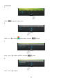
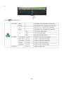
21.5" LCD Monitor
AOC e2250Sw
Service
Service
Service
Horizontal Frequency
30 - 83kHz
Table of Contents
Description
Page Description
Page
Table of Contents…………………..…………………..…...1
6.1.Main Board..…….…...........................................31
Revision List.…...................................................……......2
6.2.Power Board..……….........................................35
Important Safety Notice.….….............................……......3
1.Monitor Specification..............................………............4
2.LCD Monitor Description……….…………………….......5
3.Operation Instruction.…………...................……...........6
7.PCB Layout..………..............................................37
7.1.Main Board………..…........................................37
7.2.Power Board….…..............................................39
3.1.General Instructions....................................…...........6
7.3.Key Board………..…..........................................40
3.2.Control Buttons and Connections...............................6
8.Maintainability………............................................41
3.3.OSD Setting…..........................................................8
8.1.Equipments and Tools Requirement…...............41
4.Input/Output Specification...............……………….......24
8.2.Trouble Shooting…..………...............................42
4.1.Input Signal Connector...............………..................24
4.2.Preset Display Modes……..........................25
4.3.Panel Specification…………..………………………..26
5.Block Diagram….........................................................29
9. FOS Testing………………………………………46
10.Firmware and DDC Instruction……………….….50
11.White-Balance,Luminance Adjustment…............61
5.1.Main Board…..….............................................29
12.Mechanical Instructions …............ ..............63
5.2.Power Board…………..…………………………......30
13.Monitor Exploded View……................................71
6.Schematic…………..….........................................31
14.BOM List…………..……………………….............72
SAFETY NOTICE
ANY PERSON ATTEMPTING TO SERVICE THIS CHASSIS MUST FAMILIARIZE HIMSELF WITH THE
CHASSIS AND BE AWARE OF THE NECESSARY SAFETY PRECAUTIONS TO BE USED WHEN SERVICING
ELECTRONIC EQUIPMENT CONTAINING HIGH VOLTAGES.
CAUTION: USE A SEPARATE ISOLATION TRANSFOMER FOR THIS UNIT WHEN SERVICING
1
Revision List
Version
Release Date
Revision History
TPV Model Name
TIBARV2QAGA42NE
A00
Jun.-07-2011
Initial release
TIBARV2QAGA14NE
TIBARV2QAGA24NE
TIBARV2QAGA32NE
2
Important Safety Notice
Proper service and repair is important to the safe, reliable operation of all AOC Company Equipment. The service
procedures recommended by AOC and described in this service manual are effective methods of performing service
operations. Some of these service operations require the use of tools specially designed for the purpose. The
special tools should be used when and as recommended.
It is important to note that this manual contains various CAUTIONS and NOTICES which should be carefully read in
order to minimize the risk of personal injury to service personnel. The possibility exists that improper service
methods may damage the equipment. It is also important to understand that these CAUTIONS and NOTICES ARE
NOT EXHAUSTIVE. AOC could not possibly know, evaluate and advise the service trade of all conceivable ways in
which service might be done or of the possible hazardous consequences of each way. Consequently, AOC has not
undertaken any such broad evaluation. Accordingly, a servicer who uses a service procedure or tool which is not
recommended by AOC must first satisfy himself thoroughly that neither his safety nor the safe operation of the
equipment will be jeopardized by the service method selected.
Hereafter throughout this manual, AOC Company will be referred to as AOC.
WARNING
Use of substitute replacement parts, which do not have the same, specified safety characteristics may create shock,
fire, or other hazards.
Under no circumstances should the original design be modified or altered without written permission from AOC.
AOC assumes no liability, express or implied, arising out of any unauthorized modification of design.
Servicer assumes all liability.
FOR PRODUCTS CONTAINING LASER:
DANGER-Invisible laser radiation when open AVOID DIRECT EXPOSURE TO BEAM.
CAUTION-Use of controls or adjustments or performance of procedures other than those specified herein may
result in hazardous radiation exposure.
CAUTION -The use of optical instruments with this product will increase eye hazard.
TO ENSURE THE CONTINUED RELIABILITY OF THIS PRODUCT, USE ONLY ORIGINAL MANUFACTURER'S
REPLACEMENT PARTS, WHICH ARE LISTED WITH THEIR PART NUMBERS IN THE PARTS LIST SECTION OF
THIS SERVICE MANUAL.
Take care during handling the LCD module with backlight unit
-Must mount the module using mounting holes arranged in four corners.
-Do not press on the panel, edge of the frame strongly or electric shock as this will result in damage to the screen.
-Do not scratch or press on the panel with any sharp objects, such as pencil or pen as this may result in damage to
the panel.
-Protect the module from the ESD as it may damage the electronic circuit (C-MOS).
-Make certain that treatment person’s body is grounded through wristband.
-Do not leave the module in high temperature and in areas of high humidity for a long time.
-Avoid contact with water as it may a short circuit within the module.
-If the surface of panel becomes dirty, please wipe it off with a soft material. (Cleaning with a dirty or rough cloth may
damage the panel.)
3
1.Monitor Specifications
4
2.LCD Monitor Description
The LCD monitor will contain a main board, a Power board and a key board which house the flat panel control logic,
brightness control logic and DDC.
The power part will provide AC to DC Inverter voltage to drive the backlight of panel and the main board chips each
voltage.
Monitor Block Diagram
LED Drive.
Flat Panel and
LED backlight PLPC board
RS232 Connector
Main Board
For white balance
adjustment in factory
Key Board
AC-IN
100V-240V
HOST Computer
5
Video signal, DDC
3. Operating Instructions
3.1 General Instructions
Press the power button to turn the monitor on or off. The other control knobs are located at front panel of the monitor
(See Figure ). By changing these settings, the picture can be adjusted to your personal preferences.
* The power cord should be connected.
* Press the power button to turn on the monitor. The power indicator will light up.
3.2 Control Buttons and Connections
Power
Press the Power button to turn on/off the monitor.
Eco (DCR)/ Press the Eco key continuously to select the Eco mode of brightness and DCR on when there is no OSD. ( Eco
mode hot key may not be available in all models).
4:3 or Wide/+
When there is no OSD, press + continuously to change 4:3 or wide image ratio. (If the product screen size is 4:3 or
input signal resolution is wide format, the hot key is disable to adjust. )
Auto / Exit
When the OSD is closed,. Press Auto button continuously to do auto configure (Only for the models with dual or
more inputs).
6
1. Power
2. Analog (DB-15 VGA cable)
To protect equipment, always turn off the PC and LCD monitor before connecting.
1
Connect the power cable to the AC port on the back of the monitor.
2
Connect one end of the 15-pin D-Sub cable to the back of the monitor and connect the other end to the
computer's D-Sub port.
If your monitor displays an image, installation is complete. If it does not display an image, please refer
Troubleshooting.
7
3.3 OSD Setting
Basic and simple instruction on the control keys.
1) Press the MENU-button to activate the OSD window.
2) Press - or + to navigate through the functions. Once the desired function is highlighted, press the MENU-button to
activate it . press - or + to navigate through the sub-menu functions. Once the desired function is highlighted, press
MENU-button to activate it.
3) Press - or + to change the settings of the selected function. Press AUTO to exit. If you want to adjust any other
function, repeat steps 2-3.
4) OSD Lock Function: To lock the OSD, press and hold the MENU button while the monitor is off and then press
power button to turn the monitor on. To un-lock the OSD - press and hold the MENU button while the monitor is off
and then press power button to turn the monitor on.
Notes:
1) If the product has only one signal input, the item of "Input Select" is disable to adjust.
2) If the product screen size is 4:3 or input signal resolution is wide format, the item of "Image Ratio" is disable to
adjust.
3) One of DCR, Color Boost, and Picture Boost functions is active, the other two function is turned off accordingly.
8
Luminance
1
(Menu) to display menu.
Press
2
Press
or
to select
(Luminance), and press
to enter.
3
Press
or
to select submenu, and press
or
to adjust.
4
Press
to enter.
5
Press
two times to exit.
10
Image Setup
1
Press
(Menu) to display menu.
2
Press
or
to select
(Image Setup), and press
3
Press
or
to select submenu, and press
or
to adjust.
to enter.
4
Press
11
to enter.
5
Press
two times to exit.
12
Color Setup
1
Press
(Menu) to display menu.
2
Press
or
to select
(Color Setup), and press
to enter.
3
Press
or
to select submenu, and press
or
to adjust.
to enter.
4
Press
13
5
Press
two times to exit.
14
Picture Boost
1
Press
(Menu) to display menu.
2
Press
or
to select
(Picture Boost), and press
or
to select submenu, and press
or
to adjust.
3
Press
to enter.
4
Press
15
to enter.
5
Press
two times to exit.
16
OSD Setup
1
Press
(Menu) to display menu.
2
Press
or
to select
(OSD Setup), and press
or
to select submenu, and press
or
to adjust.
3
Press
to enter.
4
Press
17
to enter.
5
Press
two times to exit.
18
Extra
1
Press
(Menu) to display menu.
2
Press
or
to select
(Extra), and press
to enter.
3
Press
or
to select submenu, and press
to enter.
4
Press
or
to adjust.
19
5
Press
two times to exit.
20
Exit
1
Press
(Menu) to display menu.
2
Press
or
to select
(Exit), and press
to enter.
3
Press
two times to exit
21
LED Indicators
Status
LED Color
Full Power Mode
Green or Blue
Active-off Mode
Orange or red
e-Saver
Welcome to use AOC e-Saver monitor power management software! The AOC e-Saver features Smart Shutdown
functions for your monitors, allows your monitor to timely shutdown when PC unit is at any status (On, Off, Sleep or
Screen Saver); the actual shutdown time depends on your preferences (see example below).
Please click on "driver/e-Saver/setup.exe" to start installing the e-Saver software, follow the install wizard to
complete software installation.
Under each of the four PC status, you may choose from the pull-down menu the desired time (in minutes) for your
monitor to automatically shutdown. The example above illustrated:
1) The monitor will never shutdown when the PC is powered on.
2) The monitor will automatically shutdown 5 minutes after the PC is powered off.
3) The monitor will automatically shutdown 10 minutes after the PC is in sleep/stand-by mode.
4) The monitor will automatically shutdown 20 minutes after the screen saver appears.
You can click “RESET” to set the e-Saver to its default settings like below.
22
Question
e-sensor no power
interface show e-sensor
it can’t your monitor to turn off
or dark while you are away
Answer
1. Into the factory mode,set Burn in to OFF;
2. Set e-sensor to ON.
The detecting range is too near or far and the User is far away the
monitor, reset the examination area.
1. Please do not block the e-Sensor on the LOGO, which is located on
the left of AOC logo.
2. The detecting range is too far or the things blocks monitor , reset the
examination area.
Screen+
Welcome to "Screen+" software by AOC, Screen+ software is a desktop screen splitting tool, it splits the desktop
into different panes, each pane displays a different window. You only need to drag the window to a corresponding
pane, when you want to access it. It supports multiple monitor display to make your task easier. Please follow the
installation software to install it.
23
4. Input/Output Specification
4.1 Input Signal Connector
Analog connector
24
4.2 Preset Display Modes
25
4.3 Panel Specification
4.3.1 General Features
The M215HW01 model is a 21.5 inch wide TFT-LCD module with LED Backlight Unit and a 30-pin 2ch-LVDS
interface. This module supports 1920 x 1080 Full HD (16:9 wide screen) mode and displays up to 16.7 millions
colors. All input signals are 2-channel LVDS interface .
4.3.2 GENERAL SPECIFICATIONS
4.3.3 Electrical Characteristics
Electrical characteristics
Note 1: Measurement conditions:
The duration of rising time of power input is 470us.
26
Note 1: LVDS Signal Waveform
27
LED array electrical characteristics
Note (1) The LED can work normally if the PWM dimming ratio range is from 0% to 100% and the operation current
is 60mA.
Note (2) PLED = (ILED ×4) × VLED , LED matrix is 15S4P.The lightbar used by backlight unit.
Note (3) The lifetime of LED is defined as the time when it continues to operate under the conditions at Ta = 25 ±2℃
and I =
60 mA(Per EA) until the brightness becomes ≤50% of its original value.
Note(4): Pulse Width ≦10 msec and Duty ≦ 1/10
Note(5):Voltage &Temperature curve
4.3.4 Optical Characteristics
28
5. Block Diagram
5.1 Main Board
XGA/SXGA
CMVCC1
LVDS OUTPUT
DSUB_R+
DSUB_RDSUB_G+
DSUB_GDSUB_SOG
DSUB_B+
DSUB_BDSUB_H
DSUB_V
DDC1_SDA
DDC1_SCL
DET_CABLE
DSUB_R+
DSUB_RDSUB_G+
DSUB_GDSUB_SOG
DSUB_B+
DSUB_BDSUB_H
DSUB_V
DDC1_SDA
DDC1_SCL
DET_CABLE
EDID_CTRL
EDID_CTRL
VCC1.2
VCC3.3
VCC1.2
VCC3.3
CMVCC1
CMVCC1
CMVCC1
02.Input
04.Output
VCC1.2
VCC3.3
VCC1.2
CMVCC
PA[0..1]
on_BACKLIGHT
VCC3.3
Mute
Volume#
PANEL_ID#
CMVCC1
CMVCC
on_BACKLIGHT
Mute
Volume#
PANEL_ID#
Adj_BACKLIGHT
Adj_BACKLIGHT
VCTRL
VCTRL
CMVCC
PA[0..1]
PA[0..1]
PA[4..9]
PA[4..9]
PA[4..9]
PB[0..9]
PB[0..9]
CMVCC
PB[0..9]
PPWR_ON#
PPWR_ON#
L/T_SCL
L/T_SCL
L/T_SDA
L/T_SDA
CMVCC1
04.Output
05.Pow er
03.Scalar
OEM MODEL AOC 50 ID(1A)
Size
絬隔瓜絪腹
T P V ( Top
715G4737-M0B-000-0040_101028
TPV MODEL
AOC 50 ID(1A)
Rev
Key Component
01.Top
PCB NAME
715G4737-M0B
Date
Victory
Electronics
Co . ,
Ltd. )
Sheet
Friday , Nov ember 12, 2010
29
3
of
7
称爹
A
A
<称爹>
5.2 Power Board
AC input
EMI filter
Bridge
Rectifier
and Filter
Transformer
(T901)
Rectifier
diodes
14.5
5V
Start Resistor
(R908,R911)
PWM Control
LD7576AGR
(U901)
Feedback
Circuit
Power Switch
(Q901)
Photo coupler
(U902)
14.5V
L801
D801
C809
MOSFET
(Q801)
ON/OFF
DIM
Regulator
(IC903)
PWM Control
OZ9998BGN
(U801)
30
LED
(CN804)
6. Schematic
6.1 Main Board
715G4737M01BRA004C
FB102
H_Sy nc
V_Sy nc
R101 0R05 1/10W
R102 100R 1/16W 5%
R103 100R 1/16W 5%
R105
2K2 1/16W 5%
DSUB_H
DSUB_V
VGA_B+
5
5
1
BEAD
R104
2
R107
R106
C102 C103
2K2 1/16W 5%
22PF 50V
22PF 50V
C101
100R 1/16W 5%
C104
75 OHM +-5% 1/16W
VGA_B-
5PF 50V
R108
5
10
4
9
3
8
2
7
1
6
14
ミΑCONN
13
DSUB_SDA
12
DSUB_5V
VGA_B+
VGA_BVGA_G+
VGA_GVGA_R+
VGA_R-
C106
22NF25V
1K 1/16W 5%
ZD103
FB103
VGA_G+
1
RLZ5.6B
BEAD
R111
2
75 OHM +-5% 1/16W
5PF 50V
R114
FB101
U103
DSUB_SCL
1
2
3
CH1 CH4
VN
VP
CH2 CH3
6
5
4
H_Sy nc
ESD_5V
V_Sy nc
VGA_R+
1
BEAD
DSUB_G+
5
DSUB_G-
5
DSUB_R+
5
DSUB_R-
5
C109
C114
AOZ8902CIL
候綼 U1 0 3
C110
100R 1/16W 5%
C111
75 OHM +-5% 1/16W
NC
47nF 16V
R115
2
R116
VGA_R-
47nF 16V
5PF 50V
R117
C113
100R 1/16W 5%
47nF 16V
U102
CH1 CH4
VN
VP
CH2 CH3
6
5
4
VGA_PLUG
ESD_5V
VGA_B+
C115
AOZ8902CIL
候綼 U1 0 2
DSUB_5V
CMVCC1
C435
1N50V
NC
D403
LBAV70LT1G
ESD_5V
CMVCC1
DSUB_SCL R475
DSUB_SDA R476
5
5
DDC1_SDA
DDC1_SCL
R474
22K 1/16W 5%
VGA_R+
1
2
3
R473
4K7 1/16W 5%
VGA_G+
R472
4K7 1/16W 5%
DGND
5
47nF 16V
100R 1/16W 5%
GND POWER
DSUB_SOG
C107
100R 1/16W 5%
C108
R112
VGA_G-
DSUB_SDA
5
R109
17
11
DSUB_B47nF 16V
DSUB_5V
VGA_PLUG
2
15
1
16
DSUB_SCL
5
C105
100R 1/16W 5%
CN101
D-SUB 15P
DSUB_B+
47nF 16V
CMVCC1
C434
220N16V
U405
8
7
6
5
47R 1/16W 5%
47R 1/16W 5%
VCC
WP
SCL
SDA
R118
100K 1/16W 5%
1
2
3
4
A0
A1
A2
GND
5
VGA_PLUG
DET_CABLE
FM24C02A
DDC1_SDA
DDC1_SCL
Q407
LMBT3904LT1G
TPV
OEM MODEL AOC 50 ID(1A)
Size
絬隔瓜絪腹
715G4737-M0B-000-0040_101028
TPV MODEL
AOC 50 ID(1A)
Rev
Key Component
02.Input
PCB NAME
715G4737-M0B
Date
31
( Top
Victory
Electronics
Co . ,
Friday , Nov ember 12, 2010
Ltd. )
EDID_CTRL
Sheet
4
of
7
称爹
B
A
<称爹>
5
U402
SST
Eon
For user data, WB, EDID,
HDCP are saved in
Flash.
VCC3.3
AVDD
VCC1.2
6
Eon
U402
For All model
3
3
3
3
3
3
3
3
3
3
3
13
12
10
9
11
8
7
16
17
18
19
DSUB_R+
DSUB_RDSUB_G+
DSUB_GDSUB_SOG
DSUB_B+
DSUB_BDSUB_H
DSUB_V
DDC1_SDA
DDC1_SCL
R+
RG+
GSOG0
B+
BHSY NC0
VSY NC0
DDCA_SDA/RS232_TX
DDCA_SCL/rs232_RX
7
DVDD12
DVDD12
For ID2008 ID2009
PVDD33
Befor AOC ID2007 OSD
020A
ADC_VDD33
010A
020
51
U402
30
53
VCC3.3
SST
LDO_CTL
TXE3+
TXE3-
52
33
34
VCTRL
35
36
37
38
39
40
PA4
PA5
PA6
PA7
PA8
PA9
VCC3.3
4
R403 390R 1/16W 1%
AVDD
VCC3.3
R487
10K 1/16W 5%
C408
220N16V
100N16V
1
2
3
4
WP
CMVCC1
8
R489
CE# VDD 7
R490
SO HOLD# 6
R491
WP# SCK 5
R492
GND
SI Pm25LD020C-SCE
R405
MSCL
R451
L/T_SCL
R494
22R 1/16W 5%
22R 1/16W 5%
22R 1/16W 5%
22R 1/16W 5%
100R 1/16W 5%
NC
NC
+
4
R417
R453
VCC3.3
14
REXT
ADC_GND
NC/10K 1/16W 5%
21
22
23
24
28
29
54
C411 20pF 50V
C412 20pF 50V
R401
0R05 1/16W
X401
14.31818MHZ/32PF
1
PA[0..1]
5
PA[4..9]
5
PB[0..9]
PB0
PB1
PB2
PB3
PB4
PB5
PB6
PB7
PB8
PB9
C404
100N16V
7
VCC1.2
C406
C407
100N16V
100N16V
5
EE_WP
ADC_REF
R425
C418
NC
NC
VCC3.3
U401
RTD2270LW-GR
LVDS
SPI_SDO
SPI_CE
SPI_SCL
SPI_SDI
R454
NC
P5.0//PWM0
P5.1/PWM1
P3.3
P5.3/PWM3
P6.0/ADC0
P6.1/ADC1
P6.2/ADC2
P5.2/PWM2
P1.0/T2
RST
P6.3
P5.4
P5.5/PWM5
P3.2
P1.1
NC
2
C410
NC/10UF 50V
1
CMVCC1
15
U402
R408
10K 1/16W 5%
7
C401
C403
VCC1.2
PB[0..9]
41
42
43
44
45
46
47
48
49
50
30OHM
100N16V
PA[4..9]
TXO3+
TXO3TXOC+
TXOCTXO2+
TXO2TXO1+
TXO1TXO0+
TXO0-
7
PA0
PA1
PA[0..1]
TXE2+
TXE2TXE1+
TXE1TXE0+
TXE0-
AVDD
FB401
VCC3.3
XIN
20
27
R424
NC
55
56
on_BACKLIGHT
adj_BACKLIGHT
57
58
59
R485
R411
R412
4K7 1/16W 5%
100R 1/16W 5%
100R 1/16W 5%
60
61
62
63
64
R414
R410
R418
R420
R419
10K 1/16W 5%
10K 1/16W 5%
NC/100R 1/16W 5%
100R 1/16W 5%
NC/100R 1/16W 5%
7
7
R426
NC
R452
NC
R493
NC
PANEL_ID#
L/T_SDA
EDID_CTRL
KEY 2
KEY 1
7
MSDA
4
LED_G/B
LED_O
POWER_KEY #
Volume#
7
Mute
7
VCC3.3
2
0R05 1/16W
R402
XOUT
C429
R455
NC
P3.7/I2C_MCL
P3.6/I2C_MDA
PPWR_ON#
DET_CABLE
100R 1/16W 5%
6
4
MSCL
MSDA
EE_WP
NC
1
2
3
4
NC/M24C04-WMN6TP
GND
GND
DGND
DGND
R413
VCC NC
WC
E1
SCL E2
SDA VSS
3
5
31
32
26
25
U403
8
7
6
5
CMVCC1
LBADC1
(KEY1)
LBADC2
(KEY2)
AUTO(2K)
1.118V
UP
0V
(0)
R466
2K2 1/16W 5%
DOWN(2K)
1.118V
MENU(1K)
0.673V
CN406
R463
R464
NC
NC
VCC3.3
R478
C416
100N16V
VCC3.3
NC/0R05 1/16W
NC/0R05 1/16W
C417
100N16V
LMBT3906LT1G
R468
CMVCC1
1
2
3
4
5
6
VCC3.3
R482
Q402
LMBT3906LT1G
R471
CN407
FB405
TOUCH_POWER
NC
R469
2K2 1/16W 5%
LED_O
FB404
LED_ORANGE/TOUCH_VCC
LED_GRN/BLUE
330OHM 1/10W
R481
0R05 1/16W
NC/CONN
NC
TOUCH_POWER
Q403
CN402
R404
NC/10K 1/16W 5%
100N16V C415
ZD403
NC/MLVS0603M04
1
2
100N16V C414
100N16V C413
Near to Connect
CN409
7
6
5
4
3
2
1
ZD402
NC/MLVS0603M04
1
2
ZD404
NC/MLVS0603M04
1
2
CONN
LED_G/B
NC/CONN
R428
3K9 +/-5% 1/16W
R427
3K9 +/-5% 1/16W
KEY1
R461
KEY2
R462
POWER_KEY#
LED_GRN/BLUE
LED_ORANGE/TOUCH_VCC
6
5
4
3
2
1
NC
R407
NC/10K 1/16W 5%
R421
3K9 +/-5% 1/16W
CN408
1
2
3
4
5
6
7
8
1
2
3
4
5
6
7
LED_ORANGE/TOUCH_VCC
470OHM +-5% 1/10W
When use touch
Key,GPIO_P07 as
to control touch
key VCC
NC
NC/CONN
ZD401
NC/RLZ5.6B
C433
NC/CONN
T P V ( Top
NC
絬隔瓜絪腹
Key Component
Date
32
Victory
Electronics
Co . ,
715G4737-M0B-000-0040_101028
03.Scalar
Wednesday , Nov ember 10, 2010
Ltd. )
OEM MODEL AOC 50 ID(1A)
Size
TPV MODEL
AOC 50 ID(1A)
Rev
PCB NAME
715G4737-M0B
Sheet
5
of
7
称爹
C
A
<称爹>
5
PANEL_VCC
PA[0..1]
PA[0..1]
PA0
PA1
5
CN405 for 18.5" panel
(single LVDS
PANEL_VCC
channel)
PA[4..9]
PA[4..9]
PA4
PA5
PA6
PA7
PA8
PA9
5
R434
300 OHM 1/4W
C420
100N16V
1
3
5
7
9
11
13
15
17
19
21
23
25
27
29
L/T_SDA
PA1
PB3
PA5
PA7
PA9
PB1
PB3
PB5
PB7
PB9
PB0
PB1
PB2
PB3
PB4
PB5
PB6
PB7
PB8
PB9
2
4
6
8
10
12
14
16
18
20
22
24
26
28
30
L/T_SDA
L/T_SCL
PA0
PA1
PB2
PB3
PA4
PA5
CN405
PB[0..9]
PB[0..9]
R477
300 OHM 1/4W
L/T_SCL
L/T_SDA
L/T_SCL
PA0
PB2
PA4
PA6
PA8
PB0
PB2
PB4
PB6
PB8
PA6
PA7
PA8
PA9
PB0
PB1
PB2
PB3
PB7
PB8
PB9
CONN
PB4
PB5
PB6
3
3
CN403
1
2
3
4
5
6
7
8
9
10
11
12
13
14
15
16
17
18
19
20
21
22
23
24
25
26
27
28
29
30
NC/CONN
CMVCC
2006-11-7 Add pull up 4K7 to MVCC
CMVCC
4
3
2
1
R433
G
S
S
S
10K 1/16W 5%
Q405
AO3401A
5
PPWR_ON#
PPWR_ON#
NC/AO4411
PANEL_VCC
5
6
7
8
R436
100K 1/16W 5%
Q411
D
D
D
D
R435
10K 1/16W 5%
7
C419
100N16V
Q404
FB402
LMBT3906LT1G
120OHM
3D
C421
+
100UF 16V
1
G
AO3401A
2
S
T P V ( Top
Victory
Electronics
Co . ,
Ltd. )
OEM MODEL AOC 50 ID(1A)
Size
Rev
絬隔瓜絪腹
715G4737-M0B-000-0040_101028
TPV MODEL
AOC 50 ID(1A)
Key Component
04.Output
PCB NAME
715G4737-M0B
Date
Friday , October 29, 2010
33
Sheet
6
of
7
称爹
A
A
<称爹>
2008/01/14
BAT99 : If 0.05A,VF=1.0V
BAV70 : If 0.05A,VF=1.0V
It's need to use Low Dropout Regulator.
CMVCC
5
CMVCC1
CN404
9
8
7
6
5
4
3
2
1
VCC3.3
VCC3.3
VCC3.3
CMVCC
CMVCC1
R450
NC
NC(R0402)
5
R449
PANEL_ID#
5
R437
R439
NC
10K 1/16W 5%
10K 1/16W 5%
C425
NC
NC
Mute
VCC1.2
R479
NC/0R05 1/4W
BKLT-EN
CMVCC1
CMVCC
CMVCC
BKLT-VBRI
BKLT-EN
C_PANEL_INDEX
Volume
Mute
R480
1.5 OHM +-5% 2WS
R465
VCC1.2
Q410
MMBT2907A
Q406
LMBT3904LT1G
on_BACKLIGHT
5
C432
Q409
MMBT2907A
R440
10K 1/16W 5%
5
5
5
+ C423
100N16V
100UF 16V
VCTRL
CONN
U406 G903T63UF
VIN
VOUT
2
VCC3.3
VCC3.3
NC
Volume
BKLT-VBRI
adj_BACKLIGHT
R442
1K 1/16W 5%
VCC3.3
R446
R441
10K 1/16W 5%
5
1
GND
3
CMVCC1
MVCC FB403
NC
R447
R486
NC/0R05 1/16W
VCC3.3
NC/10K 1/16W 5%
U404
Q408
NC/2N3904S-RTK/PS
C428
+ C426
Volume#
100UF 16V
5
100N16V
VIN
VOUT(TAB)
ADJ(GND)
3
2
1
VCC3.3
NC/G1117-33T43UF
C422
+ C427
100N16V
R448
NC/4K7 1/16W 5%
4, 5
100UF 16V
U404 can use package 223 or 252.
OEM MODEL AOC 50 ID(1A)
Size
絬隔瓜絪腹
T P V ( Top
715G4737-M0B-000-0040_101028
TPV MODEL
AOC 50 ID(1A)
Rev
Key Component
05.Power
PCB NAME
715G4737-M0B
Date
34
Victory
Electronics
Co . ,
Tuesday , Nov ember 09, 2010
Ltd. )
Sheet
7
of
7
称爹
B
A
<称爹>
6.2 Power Board
715G4744P01000001C
!
1
R929 100 OHM 1/4W
C916
R930 100 OHM 1/4W 2N2 500V
C928
2N2 500V
F801
0R05 1/4W
+14.5V
2
+
BD901
KBP208G
R903 100 OHM 1/4W
80GL22T-3
4
-
!
!
+
C907A
C907
47uF M 450V
47uF M 450V
5
D904
FR103
8
7
9
10
3
12
11
C923
1nF 50V
R909 100 OHM 1/4W
C917
R910 100 OHM 1/4W 2N2 500V
C929
2N2 500V
+
!
2
C912
100N 50V
R918
10K OHM +-5% 1/8W
NR901
NTCR
t
C906
1N 50V
2
!
C914
1N 50V
C902
1000PF/250VAC
C920
1000uF/16V
+
C922
470UF M 16V
+
D906
3
R919
220 OHM 1/8W
FB901
BEAD
2
C908
0.47UF
+5V
SRF1060
R920
1K 1/8W
1
эDIP 1/2W
1
Q901
P0765ATF
1
LD7576AGR
R917
10 OHM 1/4W
6
5
R915
22 OHM 1/4W +-5%
2
C927
47N 50V
620K 1/4W
8
4
R902
FUSE
N.C
D905 NC/31DQ06FC3
!
F902
C925
1000uF/16V
R913
5.1 OHM 1/4W
D907
1N4148
R907
1K OHM +-5% 1/8W
L906
R912 100 OHM 1/4W
R908
10K 1/4W
R921
NC/100K 1/10W 1% U901
1
HV
2 CT
3 COMP
4 CS VCC
GND OUT
R905
470OHM +-5% 1/8W
1
D908
NC/IN4148
C913
47uF/50V
ZD901
MTZJ T-72 16B
Q904
KTD1028
D902
SR515
6
1
R904
250OHM2W
C918
NC/470UF/25V
D901
SR515
D909 NC/31DQ06FC3
R933
NC
R901
620K 1/4W
!
D903
FR107
R911
10K 1/4W
+
30mH
C903
1000PF/250VAC
!
!
1
620K 1/4W
+
!
3 L901 4
2
!
!
R931
NC
R932
NC
R900
T901
POWER X'FMR
4
R906
100K
C911
1500PF2KV
+
1
3
3
2
U902
PC123X2Y FZOF
R923
220 OHM 1/4W
R914
43.2K OHM 1%
C924
0.1uF 50V
ADD C906
R924
0.47OHM2W
R916
7K5 1/8W +/-1%
R928
1K 1/8W
IC903
AS431AZTR-E1
F901
FUSE
C900
0.0022UF
C915
1
3
!
1
R935
7K5 1/8W +/-1%
!
FB902
2
BEAD
2
CN902
Wire Harness
CN901
HS1
HEAT SINK(Q901)
SOCKET
R925
2.43KOHM +-1% 1/8W
1
2
HS2
NC/HEAT SINK(D906_5V/4A)
MUTE
VOL
+5V
1
2
ON/OFF
C926
100N 50V
DIM
L907
9
8
7
6
5
4
3
2
1
F903 FUSE
+5V1
CN903
+
C921
NC/1000uF25V
+ C931
NC/470uF/16V
+5V1
1
2
3
4
CONN
FB903
HS3
HEAT SINK(D906_5V/2.5A)
1
2
GND1
GND
1
2
1
2
BEAD
T P V ( Top
Electronics
Co . ,
Ltd. )
OEM MODEL
G4744-P0B-000-0010-1-100720
TPV MODEL
Key Component
01.POWER
PCB NAME
Date
35
Victory
絬隔瓜絪腹
Tuesday , March 29, 2011
Sheet
Size
LNPCAB351AAB2
Rev
715G4497-P0B-000-0010
1
of
3
称爹
Custom
1
ODM MODEL
1
+14.5V
1
2
SK310B
C810
0.47UF 50V
S1
G1
S2
G2
R801
10K 1/8W
+
R814
10 OHM 1% 1/4W C809
2
1
2
3
4
ON/OFF
R802
300K 1/8W
R805
C802
10N 50V
FB801
BEAD
1
100K 1/8W
R818 10K 1/8W
DIM
R803
300K 1/8W
C803
1N 50V
C815
CN801
5
4
3
2
1
R806
1N 50V
C806
220N 50V
1 OHM +-5% 1/8W
VIN
VREF
STATUS
LDR
SSTCMP
ISW
PWM
ENA
ISEN1
RT
ISEN2
OVP
GND
ISET
ISEN3
ISEN4
R808
1 OHM +-5% 1/8W
R819 R820 R821
NC
NC
NC
R822
NC
NC/CONN
C811
33UF 100V 0.47UF 50V
R817
100 OHM 1/4W
C813
100PF 50V
R812
0.1R 1%
R813
6
5
4
3
2
1
C816
1000PF500V
0.1R 1%
OZ9998BGN
R809
330K 1/8W 5%
C805
R815
160K 1/8W
C808
100PF 500V
8
7
6
5
4
3
2
1
1K 1/8W
C804
0.47UF 50V
1UF/25V
R807
U801
9
10
11
12
13
14
15
16
CN803
8
APM8005KCTRG
2
BEAD
Q801
C814
100N 50V
1
CN804
CONN
7
10 OHM 1/8W
47UH
8
7
6
5
R804
C801
330uF 25V
2
D1
D1
D2
D2
+
FB802
D801
L801
C812
R816 100PF 50V
5.1K OHM 1%
R810
20K 1/8W 1%
C807
220N 50V
R811
0R05OHM1/8W
NC/CONN
CN802
1
2
NC/CONN
T P V ( Top
絬隔瓜絪腹
Key Component
Date
36
Victory
Electronics
Co . ,
Ltd. )
OEM MODEL
G4477-P0B-000-0010-1-100720
TPV MODEL
02.INVERTER
PCB NAME
Tuesday , March 29, 2011
Sheet
Custom
Size
LNPCAB351AAB2
715G4497-P0B-000-0010
2
of
3
Rev
称爹
1
ODM MODEL
7. PCB Layout
7.1 Main Board
715G4737M01BRA004C
37
38
7.2 Power Board
715G4744P01000001C
39
7.3 Key Board
715G4747K01000001C
40
8. Maintainability
8.1 Equipments and Tools Requirement
1.
Voltmeter.
2.
Oscilloscope.
3.
Pattern Generator.
4.
DDC Tool with an IBM Compatible Computer.
5.
Alignment Tool.
6.
LCD Color Analyzer.
7.
Service Manual.
8.
User Manual.
41
8.2 Trouble Shooting
1. No Power
No power
NG
Check power cable is
tightened?
Re-plug the power cable
OK
NG
Check Power “On/Off”
is “On”?
Turn on the Power “On/Off” switch
OK
NG
Check the LED
indicate is OK?
Check the AC power
OK
Replace the converter board
NG
Replace main board and check connections
NG
Replace key board and check connections
42
2. No Video (Power LED Blue)
No Video (Power LED Blue)
Press the power
button is OK?
NG
Replace the main board
OK
Replace the converter
board
OK
The end
NG
Replace the main
board and connection
OK
The end
NG
Check the LVDS/FFC
cable or panel
NG
Replace the key board
43
OK
Replace the LVDS/FFC
cable or panel
3.
DIM
DIM (image overlap, focus or flicker)
OK
Reset in factory mode
The end
NG
OK
Set to the optimal
frequency, select the
recommended frequency
The end
NG
OK
Readjust the phase and pixel
clock in the user mode
The end
NG
OK
Pull out signal cable and
check “Self Test Feature
Check” is ok?
Check the signal cable
and the PC
NG
NG
OK
Replace the main board
The end
NG
Replace the panel
OK
44
4. Color is not optimal
Color is not optimal
Color shift
Miss color
Reset the factory mode
Replace the signal cable
NG
OK
NG
In the user mode, set the” color
settings” until customer satisfy
The end
Pull out the signal cable
and check the screen
color display is normal?
NG
OK
NG
Replace the signal cable or PC
Replace the main board
45
9. FOS Testing
9.1 Brightness Measurement
Max. Brightness>250 cd/㎡(typ).
Test conditions:
- Center of display
- Video input (RGB) = 0,700V for Analog Input
- Brightness control is set to max
- Contrast control is set to max.
Min. brightness measurement:
< 45% of Max luminance (max luminance = max contrast + max brightness)
Test conditions: - Center of display
- Video input (RGB) = 0.700V for Analog Input
- Brightness control is set to min.
- Contrast control is set to min.
9.2 Patterns Testing
Item
Waterwave
noise
Mura
LCD
bubble
Condition
(Resolution, Commended
test paten)
Normal picture
1. 1920 x 1080 (60 Hz)
2. White pattern
1. 1920 x 1080 (60 Hz)
2. Black pattern or White
pattern.
1. 1920 x 1080 (60 Hz)
2. Black pattern or White
pattern
46
Abnormal Picture
Cross line
Half line
H-Line
V-Line
H-Strip
1. 1920 x 1080 (60 Hz)
2. Black pattern
1. 1920 x 1080 (60 Hz)
2. Black pattern or White
pattern
1. 1920 x 1080 (60 Hz)
2. Black pattern, Red
pattern, Green pattern or
Blue pattern.
1. 1920 x 1080 (60 Hz)
2. Black pattern or White
pattern
1 1920 x 1080 (60 Hz)
2. Black pattern, Gray scale
pattern, Red pattern, Green
pattern or blue pattern .
47
V-Strip
1. 1920 x 1080 (60 Hz)
2. Black pattern, Gray scale
pattern, Red pattern, Green
pattern or blue pattern .
Abnormal
display
1. 1920 x 1080 (60 Hz)
2. Gray scale pattern
Gray defect
1. 1920 x 1080 (60 Hz)
2. Gray scale pattern
Video noise
1. 1920 x 1080 (60 Hz)
2. Gray scale pattern
Color tint
1. 1920 x 1080 (60 Hz)
2. Gray scale pattern
48
Gray scale
failure
Light
leakage
Fuzzy
video
1. 1920 x 1080 (60 Hz)
2. Gray scale pattern
1. 1920 x 1080 (60 Hz)
2. Black pattern or White
pattern
1. 1920 x 1080 (60 Hz)
2. Pane picture
49
10. Firmware and DDC Instruction
11. Firmware and DDC Instruction
10.1Firmware Instruction(TSUM IC ISP for exemple Milo Qw1904e)
Step 1:Tool list:
1. ISP board715GT034-B.
2. Printer cable and VGA cable
3. Adapter cable(12V)
4. Two three-core cables
Reference picture as below:
Step2: Software list:
1. LPT driver
2. Realtek_ISP_Tool_V2.2
Step3: Setup Software and Connection:
1. Setup LPT driver:run Port95nt icon:
2. LPT cable connect PC and ISP board ,VGA cable connect monitor and ISP board , picture as below:
50
3. double-click Realtek_ISP_Tool_V2.2
。
Step4: Program:
1. Run realtek_ISP_Tool_V2.2,interface as below:
2. Press down the Ctrl+Alt at the keyboard , in turn, choice Interface→CVT IIC;MCU Type→Serial Flash;
Option→1TO1;ISP Type→Auto;ISP Address→0x94;File Type→Bin。
51
3. Click “Flash Protect” and interface show dialog box,in turn, choice Value→High;Series→LPA series;Pin
List→Pin28;Click “OK”。
4. Click “BigBin”, show as follow picture, then choose correct software to click “open”,
52
5. Then, Click “Save Settings”, as below,
53
6. Show the interface as follows after press the
icon:
7. It’s successfully if interface show PASS.
54
10.2 DDC Instruction(For exemple:Philips 201B)
Tool list:
1. DDC board:715GT034-B
2. Software (WA.DAT&WD.DAT&*. CONFIG.INI)
3. LPT driver software
4. LPT cable, D-SUB CABLE
5. 12V( Adapter)
6. TPVDDCHDMI and TPVDDC6.0
7. PC
8. For example:MSTAR IC TSUMO58GDJ
55
Tool picture
For VGA BURNING: DDC Board as the follow picture:
TO PC LPT
DC 12V power
VGA
Install software:
Double-click the icon “
VGA Burning:
1. Double-click “
” to install Port95nt print driver, and then restart the computer.
”, select “Analog ” show as follow picture.
56
2. Click “Load file” and select as follow picture.
57
3. Click “ok” show as follow picture.
4.Input same SN twice and date. Click “Pragram” to burn. When appear “pass” as follow picture that burning is
successful.
58
5.Click “READ” show as follow picuture.If read SN is same as before inputing and model name is same as before
that burning is successful.
59
Appear fault as follow, please check the connection of LPT cable , Tool adapter cable and LCD power.
.
Note:
If the burn software is unsuccessfulll, appear fault:
1. For VGA,the resolution will be not the best achieve.
2. For HDMI,No picture,no sound.
If program failed, in VGA mode, you can’t use the optimal resolution.
When Read is OK, program is NG, pls do take following action:
1. For VGA,cut off the 9th pin (connect the monitor).
2. For DVI, cut off the 14th pin (the shortest pin, power supply).
3. Connect the EEPROM WP pin to ground.
60
11.White- Balance, Luminance Adjustment
Approximately 30 minutes should be allowed for warm up before proceeding white balance adjustment.
How to setting MEM channel you can reference to chroma 7120 user guide or simple use “SC” key and
“NEXT” Key to modify xyY value and use “ID” key to modify the TEXT description Following is the procedure to do
white-balance adjust .
1. Setting the color temp.
A. 6500K:
Warm color temp. parameter is
x=313±30 ,y=329±30
B. 7300K
Normal color temp. parameter is x=302±30 ,y=318±30
C. 9300K
Cool color temp. parameter is
x=283±30,y=297±30
D. sRGB
sRGB color temp. parameter is x=313±30 ,y=329±30
2. Enter into the factory mode:
Press the MENU button,Pull out the power cord, then plug the power cord. Then the factory OSD will be at the
left top of the panel.
3. Biase adjustment:
Set the Contrast
to 50; Adjust the Brightness
to 90.
4. Gain adjustment:
A. Adjust Warm (6500K) color-temperature
1. Switch the chroma-7120 to RGB-Mode (with press “MODE” button)
2. Switch the MEM.channel to Channel 3 (with up or down arrow on chroma 7120)
3. The LCD-indicator on chroma 7120 will show x=313±30 ,y=329±30
4. Adjust the RED on factory window until chroma 7120 indicator reached the value R=100
5. Adjust the GREEN on factory window until chroma 7120 indicator reachedthe value G=100
6. Adjust the BLUE on factory window until chroma 7120 indicator reached the value B=100
7. Repeat above procedure (item4, 5, 6) until chroma 7120 RGB value meet the tolerance =100±2
B. Adjust Normal (7300K) color-temperature
1. Switch the chroma-7120 to RGB-Mode (with press “MODE” button)
2. Switch the MEM.channel to Channel 4(with up or down arrow on chroma 7120)
3. The LCD-indicator on chroma 7120 will show x=302±30 ,y=318±30
4. Adjust the RED on factory window until chroma 7120 indicator reached the value R=100
5. Adjust the GREEN on factory window until chroma 7120 indicator reachedthe value G=100
6. Adjust the BLUE on factory window until chroma 7120 indicator reached the value B=100
7. Repeat above procedure (item 4, 5, 6) until chroma 7120 RGB value meet the tolerance =100±2
61
C. Adjust Cool (9300K) color-temperature
1. Switch the Chroma-7120 to RGB-Mode (with press “MODE” button)
2. Switch the MEM. Channel to Channel 9 (with up or down arrow on chroma 7120)
3. The LCD-indicator on chroma 7120 will show
x=283±30,y=297±30
4. Adjust the RED on factory window until chroma 7120 indicator reached the value R=100
5. Adjust the GREEN on factory window until chroma 7120 indicator reached the value G=100
6. Adjust the BLUE on factory window until chroma 7120 indicator reached the value B=100
7. Repeat above procedure (item 4, 5, 6) until chroma 7120 RGB value meet the tolerance =100±2
D. Adjust sRGB color-temperature
1. Switch the chroma-7120 to RGB-Mode (with press “MODE” button)
2. Switch the MEM.channel to Channel 10 (with up or down arrow on chroma 7120)
3. The LCD-indicator on chroma 7120 will show x=313±30 ,y=329±30
4. Adjust the RED on factory window until chroma 7120 indicator reached the value R=100
5. Adjust the GREEN on factory window until chroma 7120 indicator reachedthe value G=100
6. Adjust the BLUE on factory window until chroma 7120 indicator reached the value B=100
7. Repeat above procedure (item 4, 5, 6) until chroma 7120 RGB value meet the tolerance =100±2
E. Turn the Power-button off to quit from factory mode.
62
12.Mechanical Instructions
1. Put the monitor on the EPE pad.
2. Lay down the monitor and the bottom side faces to Yourself.
63
3. Pinch the hook and remove the base.
4. Use fixture to leave off the stand.
64
5. Use fixture to remove the hinge cover.
6. Remove the screws of the stand.
65
7. Remove the screws of the back cover.
8. Overturn the monitor and the top towards to yourself, and then take apart the front frame with hands.
66
9. Prize up the front frame use fixture.
10. Overturn the monitor and take off the back cover.
67
11. According to the different defective area to take off the KEPC, light line, LVDS, Hexagon screws, CBPC or
PWPC to repair.
(1)Remove the KEPC.
(2)Pull the light line out.
68
(3)Remove the Hexagon screws.
(4)Remove the LVDS.
69
(5)Overturn the iron plate and remove the screws, PWPC and CBPC.
70
12. Monitor Exploded Views
71
14. BOM List
Note: The parts information listed below are for reference only, and are subject to change without notice. Please go
to http://cs.tpv.com.cn/hello1.asp for the latest information.
TIBARV2QAGA42NE
Location
E08902
E08902
E08901
E08907
E09504
E09504
E09504
E750
E08907
Part No.
040G 58162435A
705GHABCA78
705GHABCP78
KEPCAHB5K
040G 45762420A
040G 58162435A
040G 581689 4A
045G 77500
045G 77501
052G 1185
052G 2191 A
089G 725CAA DB CKD
089G 725HAA DB CKD
089G424A15N IS
095G179J30NE34
095G8014 6DE45
095G8014 6TE45
095G8014 6WE45
0D1G1030 8120
0M1G 930 8 47 CR3
0M1G1140 8120
0Q1G 140 12120
0Q1G 930 10120
750GBU215H1B2HN000
A15G1587101
A15G1597101802 CKD
A33G1181ABJ 1L0100
A33G1182 1 1L0100
A33G1183ABJ 1L0100
A33G1184ABJ 1L0100
A34G2530ABJ 1B0100
A34G2547AEDC2B0100
A34G2548ABJ AB0100
A34G2549AED 1B0100
A37G0241014
AM1G1740 10125
H40G 58361513A
H40G22NP61578A
H41G780061554A
H45G 77 6
H45G 87 1 26
H45G 87 28 V2
H52G1801 16006
H70G201161520A
PLPCBB581AHD1
Q12G6600 6
Q52G6019 14
Q52G6025 13155
S95G179T30NE34
Description
P/N LABEL FOR MANUAL PE BAG
Brazil ASS'Y
Brazil ASS'Y
KEY BOARD
LABEL 25x6mm
LABEL
BARCODE LABEL FOR 1
INK CARTRIDGE 300000 x130
BARCODE RIBBON
MIDDLE TAPE (Y1200141)
PAPER TAPE
D-SUB CABLE
D-SUB CABLE
AC POWER CORD 1500MM
FFC CABLE 30pin 190mm 1.0mm
HARNESS 6P(CI1406)-6P(2008) 140
HARNESS 6P(CI1406)--6P(2008) 140
HARNESS 6P(CI1406S)-6P(2008) 140
screw
SCREW 3x8
SCREW 4x8
SCREW 4X12
SCREW (T3X10)
LCD M215HW01 VBTB WH AUO
HINGE PLATE
MAIN FRAME FOR 50TH 21.5W
FUNCTION BUTTON FOR 50TH
POWER LENS FOR 50TH
STAND TOP FOR 50TH 18.5W
HINGE COVER FOR 50TH 18.5W
STAND COVER
BEZEL FOR 50TH 21.5W
REAR COVER
BASE CKD
HINGE 21.5
SCREW
win7 EPEAT EPA LABEL
e2250Sw MAX ID LABEL
BRAZIL WARRANTY CARD
PE PACKING
EPE COVER
PE BAG FOR MANUAL
insulating sheet
e2250Sw CD MANUAL
POWER BOARD
FOOT
TAPE
MYLAR
FFC CABLE 30P 190mm P1.0MM
72
Remark
2nd source
2nd source
2nd source
2nd source
2nd source
CN408
CN404
CN403
CN101
X401
LED001
CN001
U402
U402
SMTCB-U402
GND1
U902
NR901
C908
C903
C902
C900
C907A
C907
C809
C801
C918
C922
L901
L906
L801
T901
CN901
D902
D901
CN902
CN902
CN804
BD901
C421
C423
C426
C427
R002
R004
R001
R003
Q901
033G3802 6B Y L
033G3802 9B Y L
033G801930F CH JS
088G 35315FVCL
093G 2253B J
709G4737 HM001
H40G 45762429A
KEPCAHB5K
081G 12 1F GP
095G820H 6TE10
709G4747 HM002
756GHBCB A1020
056G2233 11
056G2233501
100GARAI000Z11
009G6005 1
056G 139 3A
061G 5810T
063G107K474 6S
065G305M1023BW
065G305M1023BW
065G306M2222BP
067G 40Z47015K
067G 40Z47015K
067G 415330 9K
067G215D3314KV
067G215D6814KV
067G215S4713KV
073G 174 65 H2
073G 253191 H
073G 253214 DN
080GL22T 3 N3
087G 501 48 S
093G 60335
093G 60335
095G 825 9T518
095G 825 9W518
0Q1G 340 8140
311GW200A06ABX
705GHA57006
705GHA93006
709G4744 HM001
H40G 45762429A
093G 50460515
Q55G 100625
067G305M1013PB
067G305M1013PB
067G305M1013PB
067G305M1013PB
709G4737 HA001
061G0603000 FF
061G06031001FF
061G06032001FF
061G06032001FF
057G 667941
WAFER
CONN 2.0 9P
FFC CONN 1.0mm 30P R/A 34mm 6.3mm
D-SUB CONN V/T 15P BLUE H=10.4
NXS14.31818AC32F-KAB10
COMSUPTIVE ASS'Y
LABEL
KEY BOARD
LED Φ3mm 黄绿双色 GP32032M/G307-ZY-50-C
HARNESS 6P(SANW)-6P(2008) 120
COMSUPTIVE ASS'Y
MAIN BOARD-CBPCBRVA1H1K
IC Pm25LD020C-SCE SIOC-8(150mil) 2M
FLASH MX25L2026DM1I-12G 2Mb SOP-8
MCU ASS'Y-CBPCBRVA1H1K
GROUND TERMINAL
PC123Y22FZOF SHARP
RST NTCR 8 OHM +-20% 4A 13mm THINKING
0.47UF +-10%
CAP Y2 1NF 20% 250V Y5U
CAP Y2 1NF 20% 250V Y5U
CAP Y1 2.2NF 20% 250V Y5P
EC 47UF 20% 450V 12.5*35
EC 47UF 20% 450V 12.5*35
EC 33UF 20% 100V ED 8*12
EC 330UF 20% 25V 10*12 4000 hr
EC 680UF 20% 25V 10*20
EC 470UF 20% 16V 10X13
LINE FILTER 30mH MIN
IND CHOKE 1.1uH DADON
CHOKE COIL 47UH 10% LZ.CC013.G01
X'FMR 490UH 7% 4UH YUVA-1656
AC SOCKET 3PIN + 3 Hole
DIODE SR515 5A/150V DO-201AD
DIODE SR515 5A/150V DO-201AD
HARNESS 9P-9P 120MM
HARNESS 9P-9P 120MM
SCREW 4.0x8.0
WAFER 2.0mm 6P
Q901 ASS"Y
D906 ASS"Y
CONSUMPTIVE ASS'Y
LABEL
BRIDGE KBP308G-C 3A 800V KBP
TIN STICK_LOW ARGENTUM
EC 100uF M 16V 6.3*7mm
EC 100uF M 16V 6.3*7mm
EC 100uF M 16V 6.3*7mm
EC 100uF M 16V 6.3*7mm
COMSUPTIVE ASS'Y
RST CHIPR MAX0R01 1/10W FENGHUA
RST CHIPR 1 KOHM +-1% 1/10W FENGHUA
RST CHIP 2KOHM 1% 1/10W FENGHUA
RST CHIP 2KOHM 1% 1/10W FENGHUA
MOSFET P0765ATF 7 650 TO-220F
73
2nd source
2nd source
HS1
HS3
D906
U901
U801
Q801
RJ801
R811
R804
R916
R806
R907
R801
R818
R928
R918
R805
R808
R807
R815
R810
R920
R919
R803
R802
R809
R905
R816
R925
F801
R917
R814
R910
R903
R909
R930
R929
R912
R911
R908
R913
R813
R812
R923
R902
R901
R900
R817
C813
C812
090G6064 1
0M1G 930 8120
090G6084 1
GP
093G 60507
0M1G 930 8120
055G 23524
Q51G 6 4509
Q55G 100625
056G 379529
056G 700 11
057G 763 92
061G0805000 JF
061G0805000 JF
061G0805100 JF
061G08051002FT
061G0805102 JF
061G0805102 JT
061G0805103 JF
061G0805103 JF
061G0805103 JF
061G0805103 JT
061G0805104 JT
061G0805109 JF
061G0805109 JF
061G0805164 JF
061G08052002FT
061G0805202 JF
061G0805221 JF
061G0805304 JF
061G0805304 JF
061G08053303FT
061G0805471 JT
061G08055101FT
061G08059101FF
061G1206000 JT
061G1206100 JT
061G12061009FF
061G1206101 JT
061G1206101 JT
061G1206101 JT
061G1206101 JT
061G1206101 JT
061G1206101 JT
061G1206103 JF
061G1206103 JT
061G1206109 JT
061G12062007FT
061G12062007FT
061G1206221 JT
061G1206624 JF
061G1206624 JF
061G1206624 JF
061G1206681 JT
065G080510131J F
065G080510131J F
HEAT SINK
SCREW 3x8
HEAT SINK
SCHOTTKY SRF1060 C0 10A 60V ITO-220AB
SCREW 3x8
WELDING FLUX WITHOUT PB
GLUE_RTV
TIN STICK_LOW ARGENTUM
AC/DC CONVERTER IC LD7576AGR SOP-7
LED DRIVER OZ9998BGN-A1-0-TR SOP-16
FET P8008HV 4A/80V SOP-8
RST CHIPR 0 OHM +-5% 1/8W FENGHUA
RST CHIPR 0 OHM +-5% 1/8W FENGHUA
RST CHIPR 10 OHM +-5% 1/8W FENGHUA
RST CHIP 10K 1/8W 1%
RST CHIPR 1K OHM +-5% 1/8W FENGHUA
RST CHIPR 1K OHM +- 5% 1/8W TZAI YUAN
RST CHIPR 10K OHM +-5% 1/8W FENGHUA
RST CHIPR 10K OHM +-5% 1/8W FENGHUA
RST CHIPR 10K OHM +-5% 1/8W FENGHUA
RST 0805 10K 5% 1/8W
RST CHIPR 100KOHM +- 5% 1/8W TZAI YUAN
RST CHIPR 1 OHM +- 5% 1/8W FENGHUA
RST CHIPR 1 OHM +- 5% 1/8W FENGHUA
RST 0805 160K 5% 1/8W
RST CHIP 20K 1/8W 1%
RST CHIPR 2KOHM +-5% 1/8W FENGHUA
RST CHIPR 220 OHM +-5% 1/8W FENGHUA
RST CHIPR 300KOHM +-5% 1/8W FENGHUA
RST CHIPR 300KOHM +-5% 1/8W FENGHUA
RST CHIP 330K 1% 1/8W
RST CHIPR 470OHM +-5% 1/8W TZAI YUAN
RST CHIP 5K1 1/8W 1%
RST CHIPR 9.1KOHM +-1% 1/8W FENGHUA
RST CHIPR MAX0R05 1/4W TZAI YUAN
RST CHIPR 10 OHM +-5% 1/4W TZAI YUAN
RST CHIP 10 OHM 1% 1/4W FENGHUA
RST CHIPR 100 OHM +-5% 1/4W TZAI YUAN
RST CHIPR 100 OHM +-5% 1/4W TZAI YUAN
RST CHIPR 100 OHM +-5% 1/4W TZAI YUAN
RST CHIPR 100 OHM +-5% 1/4W TZAI YUAN
RST CHIPR 100 OHM +-5% 1/4W TZAI YUAN
RST CHIPR 100 OHM +-5% 1/4W TZAI YUAN
RST CHIPR 10KOHM +-5% 1/4W FENGHUA
RST CHIPR 10KOHM +-5% 1/4W TZAI YUAN
RST CHIPR 1 OHM +-5% 1/4W TZAI YUAN
RST CHIPR 0.2 OHM +-1% 1/4W
RST CHIPR 0.2 OHM +-1% 1/4W
RST CHIPR 220 OHM +-5% 1/4W TZAI YUAN
RST CHIPR 620KOHM +-5% 1/4W FENGHUA
RST CHIPR 620KOHM +-5% 1/4W FENGHUA
RST CHIPR 620KOHM +-5% 1/4W FENGHUA
RST CHIPR 680 OHM +-5% 1/4W TZAI YUAN
CAP CHIP 0805 100PF J 50V NPO
CAP CHIP 0805 100PF J 50V NPO
74
C923
C914
C803
C815
C906
C915
C802
C814
C924
C912
C926
C806
C807
C927
C811
C810
C804
C808
C929
C928
C917
C916
D801
U401
U406
U103
U102
U405
U402
Q404
Q402
Q403
Q406
Q407
Q410
Q409
Q405
R481
R402
R401
R412
R413
R420
R411
R405
R117
R115
R114
R111
R108
R104
R103
R102
R109
065G080510232K
065G080510232K
065G080510232K
065G080510232K
065G080510232K
065G080510332K
065G080510332K
065G080510432K
065G080510432K
065G080510432K
065G080510432K
065G080522432K
065G080522432K
065G080547332K
065G080547432K
065G080547432K
065G080547432K
065G120610171J
065G120622272K
065G120622272K
065G120622272K
065G120622272K
093G 60S907 T
709G4744 HS001
056G 562432
056G 563149
056G 662 48
056G 662 48
056G1133531
056G2233 11
057G 417517
057G 417517
057G 417517
057G 417518
057G 417518
057G 417527
057G 417527
057G 763940
061G0402000 JT
061G0402000 JT
061G0402000 JT
061G0402101 JT
061G0402101 JT
061G0402101 JT
061G0402101 JT
061G0402101 JT
061G0402101 JT
061G0402101 JT
061G0402101 JT
061G0402101 JT
061G0402101 JT
061G0402101 JT
061G0402101 JT
061G0402101 JT
061G0402102 JT
F
Y
Y
Y
Y
Y
Y
F
F
Y
Y
Y
Y
F
T
T
T
Y
Y
Y
Y
Y
CAP 0805 1000PF 10% 50V X7R
CAP CHIP 0805 1N 50V X7R +/-10%
CAP CHIP 0805 1N 50V X7R +/-10%
CAP CHIP 0805 1N 50V X7R +/-10%
CAP CHIP 0805 1N 50V X7R +/-10%
CAP CHIP 0805 10N 50V X7R +/-10%
CAP CHIP 0805 10N 50V X7R +/-10%
CAP CHIP 0805 0.1UF K 50V X7R
CAP CHIP 0805 0.1UF K 50V X7R
CAP CHIP 0805 100N 50V X7R +/-10%
CAP CHIP 0805 100N 50V X7R +/-10%
CAP CHIP 0805 220N 50V X7R +/-10%
CAP CHIP 0805 220N 50V X7R +/-10%
CAP CHIP 0805 47NF K 50V X7R
CAP CHIP 0805 0.47UF K 50V X7R
CAP CHIP 0805 0.47UF K 50V X7R
CAP CHIP 0805 0.47UF K 50V X7R
CAP 1206 100PF 5% 500V NP0
CER 1206 2N2 500V X7R 10%
CER 1206 2N2 500V X7R 10%
CER 1206 2N2 500V X7R 10%
CER 1206 2N2 500V X7R 10%
SCHOTTKY B3100B 3A 100V SMB
CONSUMPTIVE ASS'Y
SCALER RTD2280LW-CG LQFP-64
IC G903T63UF 0.6A/3.3V SOT-223
ESD PROTECT AZC399-04S.R7G SOT23-6L
ESD PROTECT AZC399-04S.R7G SOT23-6L
EEPROM FM24C02A-SO-T-G 2K SOP-8
IC Pm25LD020C-SCE SIOC-8(150mil) 2M
Tra LMBT3906LT1G -200mA/-40V SOT-23 LRC
Tra LMBT3906LT1G -200mA/-40V SOT-23 LRC
Tra LMBT3906LT1G -200mA/-40V SOT-23 LRC
TRA LMBT3904LT1G 200mA/40V SOT-23 LRC
TRA LMBT3904LT1G 200mA/40V SOT-23 LRC
SMALLTRAN MMBT2907A -0.6 -60V SOT-23
SMALLTRAN MMBT2907A -0.6 -60V SOT-23
MOSFET AO3401A SOT-23
RST CHIPR MAX0R05 1/16W TZAI YUAN
RST CHIPR MAX0R05 1/16W TZAI YUAN
RST CHIPR MAX0R05 1/16W TZAI YUAN
RST CHIP 100R 1/16W 5% TZAI YUAN
RST CHIP 100R 1/16W 5% TZAI YUAN
RST CHIP 100R 1/16W 5% TZAI YUAN
RST CHIP 100R 1/16W 5% TZAI YUAN
RST CHIP 100R 1/16W 5% TZAI YUAN
RST CHIP 100R 1/16W 5% TZAI YUAN
RST CHIP 100R 1/16W 5% TZAI YUAN
RST CHIP 100R 1/16W 5% TZAI YUAN
RST CHIP 100R 1/16W 5% TZAI YUAN
RST CHIP 100R 1/16W 5% TZAI YUAN
RST CHIP 100R 1/16W 5% TZAI YUAN
RST CHIP 100R 1/16W 5% TZAI YUAN
RST CHIP 100R 1/16W 5% TZAI YUAN
RST CHIP 1K 1/16W 5% TZAI YUAN
75
R442
R435
R437
R439
R440
R441
R487
R433
R414
R410
R408
R118
R436
R492
R491
R490
R489
R105
R106
R466
R469
R474
R403
R421
R427
R428
R475
R476
R485
R473
R472
R107
R112
R116
R101
R468
R471
R479
R434
R477
C436
C432
C428
C422
C420
C419
C417
C416
C415
C414
C413
C407
C406
C403
C401
061G0402102 JT
061G0402103 JT
061G0402103 JT
061G0402103 JT
061G0402103 JT
061G0402103 JT
061G0402103 JT
061G0402103 JT
061G0402103 JT
061G0402103 JT
061G0402103 JT
061G0402104 JT
061G0402104 JT
061G0402220 JT
061G0402220 JT
061G0402220 JT
061G0402220 JT
061G0402222 JT
061G0402222 JT
061G0402222 JT
061G0402222 JT
061G0402223 JT
061G04023900FT
061G0402392 JT
061G0402392 JT
061G0402392 JT
061G0402470 JT
061G0402470 JT
061G0402472 JT
061G0402472 JT
061G0402472 JT
061G0402750 JT
061G0402750 JT
061G0402750 JT
061G0603000 JT
061G0603331 JT
061G0603471 JT
061G1206000 JF
061G1206301 JT
061G1206301 JT
065G040210412K
065G040210412K
065G040210412K
065G040210412K
065G040210412K
065G040210412K
065G040210412K
065G040210412K
065G040210412K
065G040210412K
065G040210412K
065G040210412K
065G040210412K
065G040210412K
065G040210412K
A
A
A
A
A
A
A
A
A
A
A
A
A
A
A
RST CHIP 1K 1/16W 5% TZAI YUAN
RST CHIP 10K 1/16W 5% TZAI YUAN
RST CHIP 10K 1/16W 5% TZAI YUAN
RST CHIP 10K 1/16W 5% TZAI YUAN
RST CHIP 10K 1/16W 5% TZAI YUAN
RST CHIP 10K 1/16W 5% TZAI YUAN
RST CHIP 10K 1/16W 5% TZAI YUAN
RST CHIP 10K 1/16W 5% TZAI YUAN
RST CHIP 10K 1/16W 5% TZAI YUAN
RST CHIP 10K 1/16W 5% TZAI YUAN
RST CHIP 10K 1/16W 5% TZAI YUAN
RST CHIP 100K 1/16W 5% TZAI YUAN
RST CHIP 100K 1/16W 5% TZAI YUAN
RST CHIP 22R 1/16W 5% TZAI YUAN
RST CHIP 22R 1/16W 5% TZAI YUAN
RST CHIP 22R 1/16W 5% TZAI YUAN
RST CHIP 22R 1/16W 5% TZAI YUAN
RST CHIP 2K2 1/16W 5% TZAI YUAN
RST CHIP 2K2 1/16W 5% TZAI YUAN
RST CHIP 2K2 1/16W 5% TZAI YUAN
RST CHIP 2K2 1/16W 5% TZAI YUAN
RST CHIP 22K 1/16W 5% TZAI YUAN
RST CHIP 390R 1/16W 1%
RST CHIP R 3K9 +/-5% 1/16W TZAI YUAN
RST CHIP R 3K9 +/-5% 1/16W TZAI YUAN
RST CHIP R 3K9 +/-5% 1/16W TZAI YUAN
RST CHIP 47R 1/16W 5% TZAI YUAN
RST CHIP 47R 1/16W 5% TZAI YUAN
RST CHIP 4K7 1/16W 5% TZAI YUAN
RST CHIP 4K7 1/16W 5% TZAI YUAN
RST CHIP 4K7 1/16W 5% TZAI YUAN
RST 0402 75R 5% 1/16W
RST 0402 75R 5% 1/16W
RST 0402 75R 5% 1/16W
RST CHIP MAX 0R05 1/10W TZAI YUAN
RST 0603 330R 5% 1/10W
RST CHIPR 470OHM +-5% 1/10W TZAI YUAN
RST CHIPR MAX0R05 1/4W FENGHUA
RST CHIPR 300 OHM +-5% 1/4W TZAI YUAN
RST CHIPR 300 OHM +-5% 1/4W TZAI YUAN
CAP CHIP 0402 100nF K 16V X7R
CAP CHIP 0402 100nF K 16V X7R
CAP CHIP 0402 100nF K 16V X7R
CAP CHIP 0402 100nF K 16V X7R
CAP CHIP 0402 100nF K 16V X7R
CAP CHIP 0402 100nF K 16V X7R
CAP CHIP 0402 100nF K 16V X7R
CAP CHIP 0402 100nF K 16V X7R
CAP CHIP 0402 100nF K 16V X7R
CAP CHIP 0402 100nF K 16V X7R
CAP CHIP 0402 100nF K 16V X7R
CAP CHIP 0402 100nF K 16V X7R
CAP CHIP 0402 100nF K 16V X7R
CAP CHIP 0402 100nF K 16V X7R
CAP CHIP 0402 100nF K 16V X7R
76
C404
C412
C411
C102
C103
C106
C408
C434
C113
C110
C109
C107
C105
C101
C104
C108
C111
FB402
FB401
FB102
FB103
FB101
D403
ZD103
E715
E715
SW005
SW004
SW003
SW002
SW001
E715
C805
C816
C911
C913
D903
F901
F902
FB801
FB802
FB901
FB902
FB903
R924
Q904
J801
J802
J803
J804
J805
J806
J807
J808
065G0402105A5K A
065G040220031J Y
065G040220031J Y
065G040222031J A
065G040222031J A
065G040222322K T
065G040222415K T
065G040222415K T
065G040247312K A
065G040247312K A
065G040247312K A
065G040247312K A
065G040247312K A
065G040247312K A
065G040250931C Y
065G040250931C Y
065G040250931C Y
071G 56K121 M
071G 59B300 M
071G 59K190 M
071G 59K190 M
071G 59K190 M
093G 64 42 L
093G 39GA01 T
709G4737 HS001
715G4737M01BRA004C
715G4737M01BRA004S
077G603S AI CJ
077G603S AI CJ
077G603S AI CJ
077G603S AI CJ
077G603S AI CJ
715G4747K01000001C
065G250K1052HT
065G517K102 2T6921
065G 2K152 2T6921
067G215Y4707KT
093G 6026T52T
084G 56 4 B
084G 56 4 B
071G 55 29
071G 55 29
071G 55 29
071G 55 29
071G 55 29
061G152M47852T SY
057G 530503 T
095G 90 23
095G 90 23
095G 90 23
095G 90 23
095G 90 23
095G 90 23
095G 90 23
095G 90 23
CAP CHIP 0402 1UF K 10V X5R
CAP 0402 20PF 5% 50V NP0
CAP 0402 20PF 5% 50V NP0
CAP 0402 22PF J 50V NPO
CAP 0402 22PF J 50V NPO
CAP MLCC 0402 22nF K 25V X7R
CAP CHIP 0402 220nF K 16V X5R
CAP CHIP 0402 220nF K 16V X5R
CAP 0402 47NF 10% 16V X7R
CAP 0402 47NF 10% 16V X7R
CAP 0402 47NF 10% 16V X7R
CAP 0402 47NF 10% 16V X7R
CAP 0402 47NF 10% 16V X7R
CAP 0402 47NF 10% 16V X7R
CAP 0402 5PF 0.25pF 50V NP0
CAP 0402 5PF 0.25pF 50V NP0
CAP 0402 5PF 0.25pF 50V NP0
CHIP BEAD 120OHM 6A MGLB2012-120T-LF
CHIP BEAD 0603 30ohm 25% 1000mA
CHIP BEAD 0603 19R/500mA
CHIP BEAD 0603 19R/500mA
CHIP BEAD 0603 19R/500mA
DIODE LBAV70LT1G SOT-23 LRC
RLZ5.6B
COMSUPTIVE ASS'Y
MAIN PCB FR4 DS 72*65*1.6mm
MAIN PCB FR4 DS 72*65*1.6mm
TACT SWITCH AI 2PIN SEALED
TACT SWITCH AI 2PIN SEALED
TACT SWITCH AI 2PIN SEALED
TACT SWITCH AI 2PIN SEALED
TACT SWITCH AI 2PIN SEALED
KEY PCB FR1 SS 135*11*1.6mm
CAP CER 1UF 10% 25V X7R
CAP CER 1000PF K 500V Y5P
CAP CER 1500pF K 2KV Y5P
EC 47uF 20% 50V 6.3*11mm
CTIFIER DIODE FR107
FUSE 4A 250V
FUSE 4A 250V
FERRITE BEAD
FERRITE BEAD
FERRITE BEAD
FERRITE BEAD
FERRITE BEAD
RST MOFR 0.47 OHM +-5% 2WS FUTABA
2SD1207T
JUMPER WIRE
JUMPER WIRE
JUMPER WIRE
JUMPER WIRE
JUMPER WIRE
JUMPER WIRE
JUMPER WIRE
JUMPER WIRE
77
2nd source
J809
J810
J811
J812
J813
J814
J815
J901
J902
J903
J904
J905
J906
J907
J909
J910
J921
CN901
IC903
R915
R906
R904
C920
ZD901
D907
J908
D904
095G 90 23
095G 90 23
095G 90 23
095G 90 23
095G 90 23
095G 90 23
095G 90 23
095G 90 23
095G 90 23
095G 90 23
095G 90 23
095G 90 23
095G 90 23
095G 90 23
095G 90 23
095G 90 23
095G 90 23
006G 31500
056G 158 10 T
061G 17222052T TZ
061G152M10452T SY
061G152M25152T SY
067G 2046812KT
093G 39A6852T
093G 6452452T
095G 90 23
709G4744 HA001
715G4744P01000001C
093G 6026T52T
JUMPER WIRE
JUMPER WIRE
JUMPER WIRE
JUMPER WIRE
JUMPER WIRE
JUMPER WIRE
JUMPER WIRE
JUMPER WIRE
JUMPER WIRE
JUMPER WIRE
JUMPER WIRE
JUMPER WIRE
JUMPER WIRE
JUMPER WIRE
JUMPER WIRE
JUMPER WIRE
JUMPER WIRE
EYELET
LDO IC AZ431AZ-AE1 TO-92 150MA 40V TO-92
RST CFR 22R 5% 1/4W
RST MOFR 100KOHM +-5% 2WS FUTABA
RST MOF 250R 5% 2W
CS CAP 680uF 10V 8*11 mm
ZENER DIODES MTZJ22B DO-34
SWITCHING 1N4148-B4006 0.2A 100V DO-35
JUMPER WIRE
CONSUMPTIVE ASS'Y
PWR PCB FR1 SS 195*132*1.6MM
CTIFIER DIODE FR107
78