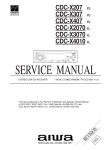
1
CDC-X447M
CDC-X507M
YU
YU
SERVICE MANUAL
STEREO CAR CD RECEIVER
BASIC CD MECHANISM : CDC02AW1
S/M Code No. 09-003-425-0R1
RE
VI
SIO
DA
N
TA
• This Service Manual is the "Revision Publishing" and replaces "Simple Manual"
(S/M Code No. 09-002-425-0T1).
SPECIFICATIONS
RADIO SECTION
AUDIO SECTION
(FM)
Frequency Range
Max. Power Output
87.5 MHz –108 MHz (100 kHz steps) *
87.5 MHz –108 MHz (50 kHz steps) *
Usable Sensitivity
12.7 dBf
50 dB Quieting Sensitivity
17.2 dBf
IF Rejection
80 dB
Frequency Response
30 Hz – 15,000 Hz
S/N Ratio
63 dB
Stereo Separation
35 dB at 1 kHz
Alternate Channel Selectivity 70 dB
Capture Ratio
3 dB
(AM)
Frequency Range
Usable Sensitivity
45 W x 4 channels
AUX IN input
Input Sensitivity (load impedance)
AUX IN
300 mV (10 kΩ)
GENERAL
Power Supply Voltage
14.4 V (11 to 16 V allowable),
DC, negative ground
Load Impedance
4Ω
Tone Control
Bass ±10 dB at 100 Hz
Treble ±10 dB at 10 kHz
Preamp Output Voltage (load impedance)
2.2 V (10 kΩ)
Installation Size
182 (W) x 53 (H) x 155 (D) mm
(71/4 (W) x 21/8 (H) x 61/8 (D) inches)
530 kHz – 1,710 kHz (10 kHz steps) *
531 kHz – 1,602 kHz (9 kHz steps) *
30 µV (30 dB)
* Set the frequency increment for your area using the switch on
the bottom of the unit.
(The switch is set at the factory to the 10 k position [for the U.S.A.])
STEERING-WHEEL-MOUNTED REMOTE CONTROL UNIT
CD SECTION
Weight
Frequency Response
Dynamic Range
Channel Separation
S/N Ratio
Wow/Flutter
Dimensions
17 Hz – 20 kHz +0/–3 dB
More than 80 dB
More than 65 dB
More than 85 dB
Unmeasurable
• Design and specifications are subject to change without notice.
ACCESSORIES / PACKAGE LIST
REF. NO. PART NO.
KANRI
DESCRIPTION
NO.
IB,INST YU,YL(3L,P)
IB,YU(3L)507M
CASE,DFP-C
HLDR,HALF-C
HLDR,REAR MTG
1
1
2
3
4
8A-KC7-902-010
8A-KCF-901-010
8Z-KC1-030-010
8Z-KC1-231-110
8Z-KC1-235-010
5
6
7
8
9
8Z-KC1-232-010
87-B10-141-010
87-B10-144-010
87-B10-145-010
87-B10-143-010
KEY,REMOVE-C
NUT,5 TYPE-2
W,5.2-10-0.5
W-SPR,5.3-8.5-1.5
UT1+5-15 W/O SLOT
10
11
12
13
*14
87-B10-216-010
8Z-KC1-244-010
8Z-KC1-250-010
8Z-KT1-616-010
R8-AZR-190-040
U+2.6-4.0 ZINC BLK(BH M2.6)
S-SCREW,5*6 TH+TAPPING ST
S-SCREW,HEXAGON
CONN ASSY,16P B52
AZR-1 RCKCGNF
Approx. 67 (W) x 26 (H) x 27 (D) mm
(23/4 (W) x 11/16 (H) x 11/8 (D) inches)
(excluding holder)
Approx. 38 g (1.33 oz.)
(including holder, battery)
* NOTE: This remote controller is not an accessory part.
It is an individual model.
–2–
PROTECTION OF EYES FROM LASER BEAM DURING SERVICING
This set employs laser. Therefore, be sure to follow carefully the
CAUTION
instructions below when servicing.
Use of controls or adjustments or performance of procedures other than those specified herin may result in
hazardous radiation exposure.
WARNING!!
WHEN SERVICING, DO NOT APPROACH THE LASER
EXIT WITH THE EYE TOO CLOSELY. IN CASE IT IS
NECESSARY TO CONFIRM LASER BEAM EMISSION.
BE SURE TO OBSERVE FROM A DISTANCE OF MORE
THAN 30cm FROM THE SURFACE OF THE OBJECTIVE
LENS ON THE OPTICAL PICK-UP BLOCK.
ATTENTION
L’utillisation de commandes, réglages ou procédures
autres que ceux spécifiés peut entraîner une dangereuse
exposition aux radiations.
ADVARSEL
Usynlig laserståling ved åbning, når sikkerhedsafbrydereer
ude af funktion. Undgå udsættelse for stråling.
Caution: Invisible laser radiation when
open and interlocks defeated avoid
exposure to beam.
Advarsel: Usynlig laserståling ved åbning,
når sikkerhedsafbrydere er ude af funktion.
Undgå udsættelse for stråling.
This Compact Disc player is classified as a CLASS 1
LASER product.
The CLASS 1 LASER PRODUCT label is located on the
rear exterior.
VAROITUS!
Laiteen Käyttäminen muulla kuin tässä käyttöohjeessa
mainitulla tavalla saataa altistaa käyt-täjän
turvallisuusluokan 1 ylittävälle näkymättömälle
lasersäteilylle.
CLASS 1
KLASSE 1
LUOKAN 1
KLASS 1
VARNING!
Om apparaten används på annat sätt än vad som
specificeras i denna bruksanvising, kan användaren
utsättas för osynling laserstrålning, som överskrider
gränsen för laserklass 1.
LASER PRODUCT
LASER PRODUKT
LASER LAITE
LASER APPARAT
Precaution to replace Optical block
(KSS – 710A)
Body or clothes electrostatic potential could
ruin laser diode in the optical block. Be sure
ground body and workbench, and use care
the clothes do not touch the diode.
1) After the connection, remove solder
shown in right figure.
Solder
–3–
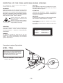
CAUTION WHEN SERVICING
1. Disassembly instructions
1) Remove the COVER, TOP and COVER, BOTTOM.
2) Remove the DFP.
3) Remove the four screws (indicated by the arrows) from the
CD mechanism. (Fig. 1)
Screw (a) x 2: VTT2.6-6
Screw (b) x 2: VTT2.6-3B
Fig. 1
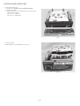
2. Servicing position
Put the DFP onto the CD CASE to fix it. (Fig. 2)
Fig. 2
–4–
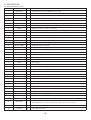
ELECTRICAL MAIN PARTS LIST
REF. NO. PART NO.
KANRI
NO.
DESCRIPTION
REF. NO. PART NO.
IC
88-KT1-606-080
8Z-KT1-622-010
87-A21-562-010
87-A21-622-030
87-020-784-080
IC,PST994D
C-IC,LC75374E
IC,LA4743B
C-IC,UPD178006AGC-540-3B9
IC,TC4053BF
88-KT1-608-010
87-A90-951-010
87-A21-467-010
87-A21-533-030
87-017-888-080
C-IC,LC75854W
RCR UNIT,SBX1971-52<507M>
C-IC,CXA2581N
C-IC,CXD2587Q
IC,NJM4558MD
87-A21-534-030
87-A21-161-040
87-A20-712-040
C-IC,UPD78012FGC-656-AB8
C-IC,BA6392FP
C-IC,BA6417F
TRANSISTOR
87-A30-287-040
87-A30-289-040
89-324-122-080
87-A30-290-010
87-A30-291-010
C-TR,DTC114TKA
C-TR,2SA1037AK(R)
C-TR,2SC2412KR
TR,KTA1658(Y)
TR,KTC4369(Y)
89-418-580-080
89-423-953-010
89-113-625-080
87-A30-283-040
87-A30-248-040
TR,2SD1858-TV2
TR,2SD2395F
C-TR,2SA1362GR
C-TR,DTA114YKA
C-TR,2SB1197KQ
87-A30-011-080
87-A30-273-040
87-026-210-040
C-TR,DTB113ZK
C-TR,DTC124EKA
C-TR,DTC144EK
DIODE
87-A40-250-080
87-A40-649-080
87-A40-624-080
87-A40-509-080
87-020-330-080
C-DIODE,DAN217
ZENER,MTZJ11A
ZENER,MTZJ10A
ZENER,MTZJ6.8C
DIODE,DAP202K
87-A40-620-080
87-A40-650-080
87-017-932-080
87-070-136-080
87-A40-798-010
ZENER,MTZJ6.2A
ZENER,MTZJ6.8A
ZENER,MTZJ6.2B
ZENER,MTZJ5.1B
DIODE,1N5402(3A/200V)
87-020-465-080
87-020-331-080
87-A40-817-040
87-A40-337-080
87-001-783-080
DIODE,1SS133
C-DIODE,DAN202K
C-ZENER,STZ6.8N
ZENER,MTZJ6.8B
DIODE,1N4002
87-020-331-080
C-DIODE,DAN202K
MAIN C.B
ANT101
C101
C102
C103
C106
8Z-KT1-614-010
87-010-178-080
87-010-197-080
87-010-186-080
87-010-198-080
ANT,AW-002
CHIP CAP,1000P
CAP,CHIP 0.01 DM
C-CAP,S 4700P-50 KB
CAP,CHIP 0.022
C107
C108
C109
C111
C112
87-010-198-080
87-018-131-080
87-010-197-080
87-010-196-080
87-010-197-080
CAP,CHIP 0.022
CAP,TC U 1000P-50 KB
CAP,CHIP 0.01 DM
CHIP CAPACITOR,0.1-25
CAP,CHIP 0.01 DM
C113
C116
C117
C118
C119
87-010-197-080
87-010-197-080
87-010-197-080
87-010-197-080
87-010-495-040
CAP,CHIP 0.01 DM
CAP,CHIP 0.01 DM
CAP,CHIP 0.01 DM
CAP,CHIP 0.01 DM
CAP,E 2.2-50 GAS
C120
C121
87-010-185-080
87-012-365-080
C-CAP,S 3900P-50 B
C-CAP,S 0.027-25VBK
–5–
KANRI
NO.
C-CAP,S
C-CAP,S
C-CAP,S
C-CAP,S
C-CAP,S
DESCRIPTION
C122
C123
C124
C131
C202
87-012-365-080
87-012-358-080
87-012-358-080
87-010-182-080
87-012-358-080
0.027-25VBK
0.47-10 FZ
0.47-10 FZ
2200P-50 KB
0.47-10 FZ
C203
C205
C206
C207
C208
87-010-196-080
87-010-553-040
87-010-198-080
87-010-196-080
87-010-196-080
CHIP CAPACITOR,0.1-25
CAP,E 47-16 GAS
CAP,CHIP 0.022
CHIP CAPACITOR,0.1-25
CHIP CAPACITOR,0.1-25
C209
C211
C212
C214
C216
87-010-196-080
87-010-198-080
87-010-196-080
87-010-196-080
87-010-198-080
CHIP CAPACITOR,0.1-25
CAP,CHIP 0.022
CHIP CAPACITOR,0.1-25
CHIP CAPACITOR,0.1-25
CAP,CHIP 0.022
C217
C218
C219
C220
C251
87-010-196-080
87-010-196-080
87-010-182-080
87-010-553-040
87-012-368-080
CHIP CAPACITOR,0.1-25
CHIP CAPACITOR,0.1-25
C-CAP,S 2200P-50 B
CAP,E 47-16 GAS
C-CAP,S 0.1-50 ZF
C252
C301
C302
C303
C304
87-010-182-080
87-012-358-080
87-012-358-080
87-010-805-080
87-010-805-080
C-CAP,S 2200P-50 B
C-CAP,S 0.47-10 FZ
C-CAP,S 0.47-10 FZ
CAP,S 1-16
CAP,S 1-16
C305
C306
C307
C308
C309
87-010-184-080
87-010-184-080
87-010-198-080
87-010-198-080
87-010-805-080
CHIP CAPACITOR,3300P(K)
CHIP CAPACITOR,3300P(K)
CAP,CHIP 0.022
CAP,CHIP 0.022
C-CAP,S 1-16 ZF
C310
C311
C312
C313
C314
87-010-805-080
87-A11-177-080
87-A11-177-080
87-A11-177-080
87-A11-177-080
C-CAP,S
C-CAP,S
C-CAP,S
C-CAP,S
C-CAP,S
C315
C316
C317
C318
C321
87-010-805-080
87-010-805-080
87-010-196-080
87-010-498-040
87-010-555-040
C-CAP,S 1-16 ZF
C-CAP,S 1-16 ZF
CHIP CAPACITOR,0.1-25
CAP,E 10-16 GAS
CAP,E 100-10 GAS
C322
C331
C332
C333
C334
87-010-198-080
87-A11-062-080
87-A11-062-080
87-A11-062-080
87-A11-062-080
CAP,CHIP 0.022
C-CAP,S 2.2-16
C-CAP,S 2.2-16
C-CAP,S 2.2-16
C-CAP,S 2.2-16
C335
C336
C337
C338
C339
87-010-491-040
87-010-491-040
87-010-805-080
87-010-805-080
87-010-805-080
CAP,E
CAP,E
CAP,S
CAP,S
CAP,S
C340
C341
C342
C343
C344
87-010-805-080
87-012-140-080
87-012-140-080
87-012-140-080
87-012-140-080
CAP,S 1-16
CAP,470P
CAP,470P
CAP,470P
CAP,470P
C401
C402
C403
C404
C405
87-010-553-040
87-012-358-080
87-012-358-080
87-010-198-080
87-010-196-080
CAP,E 47-16 GAS
C-CAP,S 0.47-10 FZ
C-CAP,S 0.47-10 FZ
CAP,CHIP 0.022
CHIP CAPACITOR,0.1-25
C406
C407
C408
C409
C410
87-010-196-080
87-012-358-080
87-012-358-080
87-010-805-080
87-010-805-080
CHIP CAPACITOR,0.1-25
C-CAP,S 0.47-10 FZ
C-CAP,S 0.47-10 FZ
C-CAP,S 1-16 ZF
C-CAP,S 1-16 ZF
C451
C452
C453
C454
C501
87-012-358-080
87-012-358-080
87-012-358-080
87-010-197-080
87-012-358-080
C-CAP,S 0.47-10 FZ
C-CAP,S 0.47-10 FZ
C-CAP,S 0.47-10 FZ
CAP,CHIP 0.01 DM
C-CAP,S 0.47-10 FZ
1-16 ZF
0.15-16
0.15-16
0.15-16
0.15-16
KB
KB
KB
KB
ZF
ZF
ZF
ZF
0.22-50 GAS
0.22-50 GAS
1-16
1-16
1-16
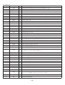
REF. NO. PART NO.
LED953
LED954
LED955
LED956
PL951
87-017-827-070
87-A40-813-040
87-A40-813-040
87-A40-813-040
8Z-KT1-641-010
KANRI
DESCRIPTION
NO.
C-LED,SEC1201C RED
C-LED,SEC1E01C BLUE
C-LED,SEC1E01C BLUE
C-LED,SEC1E01C BLUE
LAMP,T-3
CHIP CAP,1000P
CHIP CAP,1000P
CAP,S 1-16
CAP,E 10-16 GAS
C-CAP,S 0.1-50 ZF
PL952
S951
S952
S953
S954
8Z-KT1-641-010
87-036-251-080
87-036-251-080
87-036-251-080
87-A90-001-080
LAMP,T-3
SW,TACT SKQCAE
SW,TACT SKQCAE
SW,TACT SKQCAE
C-SW,TACT SKQMAL
87-012-368-080
87-012-368-080
87-012-368-080
87-A11-062-080
87-A11-062-080
C-CAP,S
C-CAP,S
C-CAP,S
C-CAP,S
C-CAP,S
S955
S956
S957
S958
S959
87-036-251-080
87-036-251-080
87-036-251-080
87-A90-001-080
87-A90-001-080
SW,TACT SKQCAE
SW,TACT SKQCAE
SW,TACT SKQCAE
C-SW,TACT SKQMAL
C-SW,TACT SKQMAL
C801
C901
C902
C903
C904
8A-KC7-623-000
87-016-039-090
87-012-358-080
87-010-196-080
87-010-315-080
CAP,E 2200U-16 BT(125C)
CAP,DL 0.022F-5.5 Z 70 FM
C-CAP,S 0.47-10 FZ
CHIP CAPACITOR,0.1-25
C-CAP,S 27P-50 CH
S960
S961
S962
S963
S964
87-A90-001-080
87-036-251-080
87-036-251-080
87-036-251-080
87-036-251-080
C-SW,TACT SKQMAL
SW,TACT SKQCAE
SW,TACT SKQCAE
SW,TACT SKQCAE
SW,TACT SKQCAE
C905
C906
C907
C908
C909
87-010-314-080
87-010-196-080
87-010-178-080
87-010-178-080
87-010-198-080
C-CAP,S 22P-50V
CHIP CAPACITOR,0.1-25
CHIP CAP,1000P
CHIP CAP,1000P
CAP,CHIP 0.022
S965
S966
S967
87-036-251-080
87-036-251-080
87-A91-597-010
SW,TACT SKQCAE
SW,TACT SKQCAE
SW,RTRY SIM-026MT
C910
C911
C912
C914
C916
87-010-322-080
87-010-322-080
87-010-198-080
87-010-198-080
87-010-198-080
C-CAP,S 100P-50 CH
C-CAP,S 100P-50 CH
CAP,CHIP 0.022
CAP,CHIP 0.022
CAP,CHIP 0.022
CON401
CON402
CON851
D909
F251
87-A61-219-010
88-KTA-603-010
8Z-KT1-611-010
87-027-262-010
8Z-KC1-621-010
CONN,20P H 52089-2020
CONN,15P CAM-B68
CONN,16P CAM-B51
LED,TLR-124(RED)
FUSE,15A 32V
FFC401
J401
J402
L101
L102
88-KC4-641-010
87-A61-224-010
8A-KC7-620-010
87-003-143-080
8Z-KT1-619-010
FF-CABLE,20P 1.0 90MM
JACK,PIN 4P XR-401
JACK,DIN 13 P SKDS1302
COIL,4.7UH
COIL,68MH K7-D
L201
L202
L301
L401
L402
87-003-149-080
87-003-102-080
87-003-102-080
87-003-102-080
87-003-102-080
COIL,47UH
COIL,10UH
COIL,10UH
COIL,10UH
COIL,10UH
L851
S901
SW903
TU101
X901
8Z-KT1-615-010
87-A91-070-010
87-A91-152-010
8A-KC8-621-010
87-A70-175-010
FLTR,AMORPHOUS-CHOKE
SW,TACT SKHHLV
SW,SL 1-1-2 SSSS212-11-A
TU UNIT,FAE347-A12
VIB,XTAL 4.5MHZ AT-49
C502
C503
C504
C505
C506
87-012-358-080
87-012-358-080
87-012-358-080
87-010-178-080
87-010-178-080
C507
C508
C509
C510
C511
87-010-178-080
87-010-178-080
87-010-805-080
87-010-498-040
87-012-368-080
C512
C513
C514
C519
C520
KANRI
DESCRIPTION
NO.
C-CAP,S 0.47-10 FZ
C-CAP,S 0.47-10 FZ
C-CAP,S 0.47-10 FZ
CHIP CAP,1000P
CHIP CAP,1000P
0.1-50
0.1-50
0.1-50
2.2-16
2.2-16
REF. NO. PART NO.
ZF
ZF
ZF
ZF
ZF
JACK AUX C.B
FC951
J951
8A-KC7-611-010
85-HRL-623-010
F-CABLE,3P(AUX)
JACK,3.5 ST BLK
C803
C804
C805
C806
C808
87-A10-711-080
87-010-178-080
87-016-669-080
87-010-184-080
87-016-669-080
C-CAP,E 100-6.3 M MF
CHIP CAP,1000P
C-CAP,S 0.1-25 K B
CHIP CAPACITOR,3300P(K)
C-CAP,S 0.1-25 K B
C809
C811
C813
C816
C831
87-010-880-080
87-016-669-080
87-016-669-080
87-010-880-080
87-012-156-080
C-CAP,E
C-CAP,S
C-CAP,S
C-CAP,E
C-CAP,S
C832
C833
C834
C835
C836
87-010-194-080
87-012-156-080
87-012-156-080
87-016-669-080
87-012-156-080
CAP,CHIP 0.047
C-CAP,S 220P-50 CH
C-CAP,S 220P-50 CH
C-CAP,S 0.1-25 K B
C-CAP,S 220P-50 CH
C837
C838
C839
C840
C841
87-010-186-080
87-010-194-080
87-010-880-080
87-016-669-080
87-016-669-080
CHIP CAPACITOR,4700P(K)
CAP,CHIP 0.047
C-CAP,E 47-6.3 MF
C-CAP,S 0.1-25 K B
C-CAP,S 0.1-25 K B
C842
C843
C844
C845
C846
87-016-526-080
87-012-155-080
87-012-155-080
87-010-177-080
87-010-177-080
C-CAP,S 0.47-16 BK
C-CAP,180P-50CH
C-CAP,180P-50CH
C-CAP,S 820P-50 SL
C-CAP,S 820P-50 SL
C847
C848
C849
C850
C851
87-010-885-080
87-010-885-080
87-010-318-080
87-010-318-080
87-A12-034-080
C-CAP,E
C-CAP,E
C-CAP,S
C-CAP,S
C-CAP,E
C852
C853
C854
C855
C856
87-A12-034-080
87-010-178-080
87-010-178-080
87-A10-473-080
87-016-669-080
C-CAP,E 2.2-35 M MF
CHIP CAP,1000P
CHIP CAP,1000P
C-CAP,E 47-10 MF10FC(M)
C-CAP,S 0.1-25 K B
C857
C861
C862
C863
87-010-880-080
87-016-669-080
87-016-669-080
87-010-880-080
C-CAP,E
C-CAP,S
C-CAP,S
C-CAP,E
CD C.B
!
FRONT C.B
C951
C952
C953
C954
C955
87-012-358-080
87-012-358-080
87-010-176-080
87-010-194-080
87-010-194-080
C-CAP,S 0.47-10 FZ
C-CAP,S 0.47-10 FZ
C-CAP,S 680P-50 SL
CAP,CHIP 0.047
CAP,CHIP 0.047
C956
C957
C958
C959
C960
87-010-194-080
87-012-358-080
87-010-197-080
87-010-197-080
87-010-194-080
CAP,CHIP 0.047
C-CAP,S 0.47-10 FZ<507M>
CAP,CHIP 0.01 DM
CAP,CHIP 0.01 DM
CAP,CHIP 0.047
CON951
L951
L952
L953
LCD951
88-KTA-602-010
87-005-906-080
87-005-906-080
87-005-906-080
8A-KCF-610-010
CONN,15P CAM-B67
C-COIL,S 10.0UHK
C-COIL,S 10.0UHK
C-COIL,S 10.0UHK
LCD,AKC-15(3 COLOR)
LED951
LED952
87-017-827-070
87-017-827-070
C-LED,SEC1201C RED
C-LED,SEC1201C RED
–6–
47-6.3 MF
0.1-25 K B
0.1-25 K B
47-6.3 MF
220P-50 CH
22-10 MF
22-10 MF
47P-50 CH
47P-50 CH
2.2-35 M MF
47-6.3
0.1-25
0.1-25
47-6.3
MF
K B
K B
MF
REF. NO. PART NO.
KANRI
DESCRIPTION
NO.
C-CAP,E 47-10 MF10FC(M)
C-CAP,S 0.1-25 K B
C-CAP,S 0.1-25 K B
CHIP CAP,1000P
C-CAP,E 47-10 MF10FC(M)
C881
C882
C883
C884
C885
87-A10-473-080
87-016-669-080
87-016-669-080
87-010-178-080
87-A10-473-080
C886
C887
C888
C889
C891
87-016-669-080
87-016-669-080
87-016-669-080
87-A10-473-080
87-012-156-080
C-CAP,S
C-CAP,S
C-CAP,S
C-CAP,E
C-CAP,S
0.1-25 K B
0.1-25 K B
0.1-25 K B
47-10 MF10FC(M)
220P-50 CH
C892
C893
C894
C895
C896
87-012-156-080
87-012-156-080
87-012-156-080
87-012-156-080
87-012-156-080
C-CAP,S
C-CAP,S
C-CAP,S
C-CAP,S
C-CAP,S
220P-50
220P-50
220P-50
220P-50
220P-50
C897
CN801
CN891
L801
L802
87-012-156-080
87-A61-125-080
87-A61-220-080
87-A50-536-080
87-A50-536-080
C-CAP,S 220P-50 CH
C-CONN,16P H FLZ-SM1-TB
C-CONN,20P H 52271-2090
C-COIL,10UH K LQH3C24
C-COIL,10UH K LQH3C24
REF. NO. PART NO.
L831
L832
L833
L861
L881
87-A50-536-080
87-A50-536-080
87-A50-536-080
87-A50-536-080
87-A50-536-080
S861
X831
X861
87-A91-627-080
87-A70-262-080
87-A70-251-080
KANRI
DESCRIPTION
NO.
C-COIL,10UH K LQH3C24
C-COIL,10UH K LQH3C24
C-COIL,10UH K LQH3C24
C-COIL,10UH K LQH3C24
C-COIL,10UH K LQH3C24
SW,PUSH MPU10372MLBO
C-VIB,16.93MHZ CSTCW
C-VIB,CER 10.00MHZ CSTCC
SENSOR C.B
CH
CH
CH
CH
CH
SW1
SW2
87-A91-627-080
87-A91-627-080
SWITCH
SWITCH
CHIP RESISTOR PART CODE
Chip Resistor Part Coding
8 8
A
Figure
Resistor Code
Value of resistor
Chip resistor
L
W
t
:A
Resistor Code : A
1.0
0.5
0.35
104
Dimensions (mm)
Wattage
1/16W
Type
1005
Tolerance
5%
Symbol
CJ
1/16W
1/10W
1608
2125
5%
5%
CJ
CJ
1/8W
3216
5%
CJ
Form
L
t
W
TRANSISTOR ILLUSTRATION
C
B
E
2SA1037
2SA1362
2SB1197
2SC2412
DTA114YKA
DTB113ZK
DTC114TKA
DTC124EKA
DTC144EK
B C E
E C B
2SD2395
KTA1658
KTC4369
2SD1858
–7–
1.6
0.8
0.45
108
2
1.25
0.45
118
3.2
1.6
0.55
128
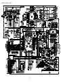
WIRING – 1 (MAIN)
32
31
30
29
28
27
26
25
24
23
22
21
20
19
18
17
16
15
14
13
12
11
10
9
8
7
6
5
4
3
2
1
A
B
C
D
E
F
G
H
I
J
K
L
M
N
O
P
Q
R
S
T
U
–8–
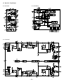
SCHEMATIC DIAGRAM – 1 (MAIN)
–9–
WIRING – 2 (FRONT / JACK AUX)
J
I
H
G
F
E
D
C
B
A
32
31
30
29
28
27
26
25
24
23
22
21
20
19
18
17
16
15
14
13
12
11
10
9
8
7
6
5
4
3
2
1
32
31
30
29
28
27
26
25
24
23
22
21
20
19
18
17
16
15
14
13
12
11
10
9
8
7
6
5
4
3
2
1
A
B
C
D
E
F
G
H
I
J
– 10 –
SCHEMATIC DIAGRAM – 2 (FRONT / JACK AUX)
– 11 –
WIRING – 3 (CD / SENSOR) <1 / 2>
32
31
30
29
28
27
26
25
24
23
22
21
20
19
18
17
16
15
14
13
12
11
10
9
8
7
6
5
4
3
2
1
A
B
C
D
E
F
G
H
I
J
K
L
M
N
O
P
Q
R
S
T
U
– 12 –
WIRING – 3 (CD) <2 / 2>
1
2
3
4
5
6
7
8
9
10
11
12
13
14
15
16
17
A
B
C
D
E
F
G
H
I
J
K
L
M
N
O
P
Q
R
S
T
U
– 13 –
18
19
20
21
22
23
24
25
26
27
28
29
30
31
32
SCHEMATIC DIAGRAM – 3 (CD / SENSOR)
– 14 –
LCD DISPLAY
No.
COM1
COM2
COM3
COM4
– 15 –
1
2
3
4
5
6
7
8
––
––
– – COM1 Bar8 Bar7
TP
2d
––
– – COM2 – – H-BASS LO
ST
2e
– – COM3 – –
––
R
L
DSSA
2f
COM4 – –
––
––
AF
TA MY INFO 1a,e,f,j,k
9
2m
2l
2j
2g
10
2n
2k
2i
2h
11
CD
2c
2b
2a
12
3d
3e
3f
–CH
13
3m
3l
3j
3g
14
3n
3k
3i
3h
15
Bar1
3c
3b
3a
25
6m
6l
6j
6g
26
6n
6k
6i
6h
27
Bar6
6c
6b
6a
28
7d
7e
7f
Dot2
29
7m
7l
7j
7g
30
7n
7k
7i
7h
No.
COM1
COM2
COM3
COM4
16
4d
4e
4f
Bar2
17
4m
4l
4j
4g
18
4n
4k
4i
4h
19
Bar3
4c
4b
4a
20
5d
5e
5f
Bar4
21
5m
5l
5j
5g
22
5n
5k
5i
5h
23
Dot1
5c
5b
5a
24
6d
6e
6f
Bar5
No.
COM1
COM2
COM3
COM4
31
Dot3
7c
7b
7a
32
8d
8e
8f
Bar9
33
8m
8l
8j
8g
34
8n
8k
8i
8h
35
Bar10
8c
8b
8a
36
9d
9e
9f
CT
37
9m
9l
9j
9g
38
9n
9k
9i
9h
39
MT
9c
9b
9a
IC BLOCK DIAGRAM
IC, LA4743B
IC, LC75854W
IC, LC75374E
– 16 –
IC, BA6392FP
IC, NJM4558MD
IC, BA6417F
IC, TC74ACT244F
IC, TC4053BF
– 17 –
IC, CXD2587Q
– 18 –
IC DESCRIPTION
IC, µPD178006AGC–540–3B9
Pin No.
Pin Name
I/O
Description
1
FM/AM S-M
I
Input RDS AF IN signal and FM/AM S meter signal.
2
LEVEL IND
I
Input level indicator signal.
3
A-VOL CONT
I
Detect mic input and operate auto volume. (Not used)
4
CD CONNECT
I
Connectivity check to CD changer.
5
CD DISP SEL
O
Communication timing signal output to CD changer ("H" = TX, "L" = RX).
6
CD CLO
O
Output synchronous clock signal for sending to CD changer.
7
CD DI
I
Input data signal for receiving from CD changer.
8
CD DO
O
Output data signal for sending to CD changer.
9
CD CLI
I
Input synchronous clock signal for receiving from CD changer.
10
LCD CE
O
LCD driver (LC75854W) : Output CE signal.
11
CLK SEL
O
CLock selection for CDS and LCD driver (LC75854W) ("H" = CDS, "L" = LCD).
12
LCD DI
I/O
13
LCD DO
O
LCD driver (LC75854W) : Output data signal.
14
LCD CLO
O
LCD driver (LC75854W) : Output synchronous clock signal.
15
CD ACC CONT
O
Output CD changer ACC signal.
16
POWER MUTE
O
Output POWER MUTE signal.
17
ST-BY MUTE
O
Output STANDBY MUTE signal.
18
POWER CONT
O
Output POWER CONTROL signal.
19
CONT1
O
LCD driver contrast controller 1.
20
CONT2
O
LCD driver contrast controller 2.
21
GND
–
GND.
22
VDD
–
Power supply.
23
MUTE
O
Output audio mute.
24
BAND CONT
O
Output AM/FM power supply switching ("H" = AM, "L" = FM).
25
RADIO CONT
O
Output radio power switching ("L" = Radio mode).
26
RDS MODE
O
Output "H" when RDS AF mode. (Not used)
27
IF REQ
O
Output request for IF count signal.
28
AM IF
I
Input AM IF count signal.
29
FM IF
I
Input FM IF count signal.
30
VDD PLL
–
Power supply for PLL.
31
FM OSC
I
Input FM local oscillation.
32
AM OSC
I
Input AM local oscillation.
33
GND PLL
–
Connected to GND for PLL.
34
EO0
O
Output error from charge pump. (Not used)
35
EO1
O
Output error from charge pump.
36
GND
–
GND.
37
LOC/DX
O
Output LOC/DX switching when seeking radio broadcast ("H" = LOC, "L" = DX).
38
SD/ST IND
I
39
PHONE MUTE
I
External mute control.
40
CDS CS
O
CDS : Output CS signal.
LCD driver (LC75854W) : Input data signal.
Input stereo signal. Enable when receiving FM broadcast ("H" = MONO, "L" = ST)/
Input FM/AM broadcast detection signal when seeking ("H" = Detect broadcast).
– 19 –
Pin No.
Pin Name
I/O
Description
41
CDS RESET
O
CDS : Output reset signal.
42
CDS SLEEP
O
CDS : Output sleep signal.
43
CDS STOP
I
CDS : Input stop signal.
44
CDS IN
I
CDS : Input disc inserted status detection.
45
TEST
I
Test point.
46 ~ 47
NC
I
Not connected.
48
LED
O
Output security LED ON/OFF ("H" = 120 ~ 130ms, 1 cycle = 3sec).
49 ~ 51
MI-1 ~ MI-3
I
Input diode matrix for initial setting.
52 ~ 54
MO-1 ~ MO-3
O
Output diode matrix for initial setting.
55
MO-4
O
Output diode matrix for initial setting. (Not used)
56 ~ 57
NC
O
Not connected.
58
ACC IN
O
Input ACC (power supply for accessory) ON/OFF.
59
BEEP
O
Output beep (3kHz, 50ms).
60
REMOTE
I
Input remote controller.
61
E-VOL CE
O
Output CE to electric volume (LC75374E).
62
E-VOL DO
O
Output data to electric volume (LC75374E).
63
E-VOL CLO
O
Output clock to electric volume (LC75374E).
64
DRV CONT
O
Output "H" when DRV status is 1/2.
65
RDS DI
I
Input RDS data (Pull down when not used).
66
DFP IN
I
Detect DFP (front panel) existence.
67
FLAP IN
I
Detect OPEN/CLOSE of FLAP DFP ("H" = DFP IN enable).
68
RDS CLI
I
Input RDS clock (Pull down when not used).
69
EJECT IN
I
Input eject detection when FLAP IN (Pin 67) is "L".
70
BATT IN
I
Input battery ON/OFF.
71
RE-1
I
Input rotary encoder 1.
72
RE-2
I
Input rotary encoder 2.
73
S-REQ
I
Input S-REQ signal.
74
REG CPU
–
Regulator for CPU power supply.
75
GND
–
GND.
76
X-OUT
O
System clock oscillator (4.5MHz) output.
77
X-IN
I
System clock oscillator (4.5MHz) input.
78
REG OSC
–
Regulator for oscillation circuit.
79
VDD
–
Power supply.
80
RESET
I
Input system reset.
– 20 –
IC, LC75374E
Pin No.
Pin Name
I/O
Description
1
RVR IN
I
4dB volume control input. Must be driven at a low impedance.
2
R COM
–
1dB volume control common pin.
For the connection of capacitors that compensate for bass and treble in the tone control circuits.
3~5
RT1 ~ RT3
–
A high-frequency compensation capacitors must be connected between RT1 and RT2.
A low-frequency compensation capacitors must be connected between RT2 and RT3.
6
RT OUT
O
Tone control output.
7
RS IN
I
Super bass input. Must be driven at a low impedance.
8
NC
–
Connected to GND.
9
NC
–
Not connected.
10 ~ 11
RSB1 ~ RSB2
–
For the connection of RCH super bass compensation capacitors.
12
FR IN
I
Fader input. Must be driven at a low impedance.
13
FR OUT
O
Fader output. The front and rear sides can be attenuated independently.
14
RR OUT
15
VSS
–
GND.
16
CL
I
Serial data and clock input for control.
17
DI
18
CE
–
19
VREF
–
20
RL OUT
21
FL OUT
22
Chip enable. Data is written in the internal latch when the chip enable signal goes "L"
from "H", and each analog switch is activated. Data transfer is enabled at "H".
Generates a 1/2VDD power source. A capacitor must be connected between VREF and
GND as a troubleshooting against power ripples.
O
Fader output. The front and rear sides can be attenuated independently.
FL IN
I
Fader input. Must be driven at a low impedance.
23 ~ 24
LSB2 ~ LSB1
–
For the connection of LCH super bass compensation capacitors.
25
NC
–
Not connected.
26
NC
–
Connected to GND.
27
LS IN
I
Super bass input. Must be driven at a low impedance.
28
LT OUT
O
Tone control output.
For the connection of capacitors that compensate for bass and treble in the tone control circuit.
29 ~ 31
LT3 ~ LT1
A high-frequency compensation capacitors must be connected between LT1 and LT2.
A low-frequency compensation capacitors must be connected between LT2 and LT3.
32
L COM
–
1dB volume control common pin.
33
LVR IN
I
4dB volume control input. Must be driven at a low impedance.
34
LSELO
O
Input selector output pin.
35
AUX(L)
36
CD(L)
I
Signal input pins.
37
TUN(L)
38
TP(L)
39
VDD
–
Power supply.
– 21 –
Pin No.
Pin Name
40
TP(R)
41
TUN(R)
42
CD(R)
43
AUX(R)
44
I/O
Description
I
Signal input pins.
RSELO
O
Input selector output pin.
Pin No.
Pin Name
I/O
1
S1
O
LCD segment output.
2
S2
O
LCD segment ouptut. (Not used)
3 ~ 37
S3 ~ S37
O
LCD segment output.
38 ~ 39
S38 ~ S39
O
LCD segment output. (Not used)
40 ~ 43
COM1 ~ COM4
O
LCD common driver output.
44 ~ 45
KS1 ~ KS2
O
Key scan output. (Not used)
46 ~ 49
KS3 ~ KS6
O
Key scan output.
50 ~ 54
KI1 ~ KI5
I
Key scan input. These pins incorporate pull-down resistors.
55
TEST
–
Test pin. (Connected to GND)
56
VDD
–
Power supply.
57
VDD1
I
58
VDD2
I
59
VSS
–
GND.
60
OSC
I
Resistor and capacitor are attached externally form an oscillator circuit.
61
DO
O
Serial data interface pin; output data.
62
CE
O
Serial data interface pin; chip enable.
63
CL
O
Serial data interface pin; synchronization.
64
DI
I
Serial data interface pin; data transferred.
IC, LC75854W
Description
2/3 bias voltage is applied to the LCD drive externally.
(Must be connected to VDD2 when a 1/2 bias drive scheme is used)
1/3 bias voltage is applied to the LCD drive externally.
(Must be connected to VDD1 when a 1/2 bias drive scheme is used)
– 22 –
IC, CXD2587Q
Pin No.
Pin Name
I/O
Description
1
SQSO
O
Sub-Q 80-bit and PCM peak/level data output. CD TEXT data output.
2
SQCK
I
Clock input for reading SQSO.
3
XRST
I
System reset. Reset at "L".
4
SYSM
I
Muting input. Muted at "H".
5
DATA
I
Serial data input from CPU.
6
XLAT
I
Latch input from CPU. Latches serial data at the trailing edge.
7
CLOK
I
Clock input for serial data transfer from CPU.
8
SENS
O
SENS output to CPU.
9
SCLK
I
Clock input for reading SENS serial data.
10
VDD
–
Power supply of digital circuits.
11
ATSK
I/O
12
SPOA
I
Microprocessor extended interface (input A). (Connected to ground)
13
SPOB
I
Microprocessor extended interface (input B). (Connected to ground)
14
XLON
O
Microprocessor extended interface (output). (Not used)
15
WFCK
O
WFCK output. (Not used)
16
XUGF
O
WUGF output. MNT1 or RFCK is output when switched by command. (Not used)
17
XPCK
O
XPCK output. MNT0 is output when switched by command. (Not used)
18
CFS
O
GFS output. MNT3 or XROF is output when switched by command.
19
C2PO
O
C2PO output. GTOP is output when switched by command.
20
SCOR
O
Outputs "H" when Sub-code sync S0 or S1 is detected.
21
COUT
I/O
Track number count signal input/output. (Not used)
22
MIRR
I/O
Mirror signal input/output. (Not used)
23
DFCT
I/O
Defect signal input/output. (Not used)
24
FOK
I/O
Focus OK signal input/output.
25
LOCK
I/O
26
MDP
O
Spindle motor servo control output.
27
SSTP
I
Disc innermost edge detection signal input. (Connected to ground)
28
SFDR
O
Sled drive output.
29
SRDR
O
Sled drive output.
30
TFDR
O
Tracking drive output.
31
TRDR
O
Tracking drive output.
32
FFDR
O
Focus drive output.
33
FRDR
O
Focus drive output.
34
VSS
–
Ground of digital circuits.
35
TEST
I
TEST pin. (Connected to ground)
36
TES1
I
TEST pin. (Connected to ground)
37
XTSL
I
38
VC
I
Neutral voltage input.
39
FE
I
Focus error signal input.
Input/output for anti-shock. (Connected to ground)
Outputs "H" when GFS sampled by 460 Hz is "H"; "L" when GFS is "L" continuously for 8
samplings. Or, a signal is input when LKIN is "1".
Crystal select input. "L" when 16.9344MHz crystal is used;
"H" when 33.8688MHz crystal is used. (Connected to ground)
– 23 –
Pin No.
Pin Name
I/O
Description
40
SE
I
Sled error signal input.
41
TE
I
Tracking error signal input.
42
CE
I
Neutral servo analog input.
43
RFDC
I
RF signal input.
44
ADIO
O
For test. (Not used)
45
AVSS0
–
Ground of analog circuits.
46
IGEN
I
Constant current input for OP amp.
47
AVDD0
–
Power supply of analog circuits.
48
ASYO
O
EFM full-swing output ("L" = VSS, "H" = VDD).
49
ASYI
I
Asymmetry comparator voltage input.
50
BIAS
I
Asymmetry circuit constant current input.
51
RFAC
I
EFM signal input.
52
AVSS3
–
Ground of analog circuits.
53
CLTV
I
VCO1 control voltage input for multiplication.
54
FILO
O
Filter output for master PLL (Slave: Digital PLL).
55
FILI
I
Filter input for master PLL.
56
PCO
O
Charge pump output for master PLL.
57
AVDD3
–
Power supply of analog circuits.
58
VSS
–
Ground of digital circuits.
59
VDD
–
Power supply of digital circuits.
60
DOUT
O
Digital output. (Not used)
61
LRCK
O
D/A interface LR clock output f=Fs. (Not used)
62
PCMD
O
D/A interface serial data output (2's COMP, MSB first). (Not used)
63
BCK
O
D/A interface bit clock output. (Not used)
64
EMPH
O
65
XVDD
–
Power supply of master clock.
66
XTAI
I
Crystal oscillator input. External master clock is input to this pin.
67
XTAO
O
Crystal oscillator output.
68
XVSS
–
Ground of master clock.
69
AVDD1
–
Power supply of analog circuits.
70
AOUT1
O
Lch analog output.
71
AIN1
I
Lch OP amp input.
72
LOUT1
O
Lch LINE output.
73 ~ 74
AVSS1, AVSS2
–
Ground of analog circuits.
75
LOUT2
O
Rch LINE output.
76
AIN2
I
Rch OP amp input.
77
AOUT2
O
Rch analog output.
78
AVDD2
–
Power supply of analog circuits.
79
RMUT
O
Rch "0" detection flag. (Not used)
80
LMUT
O
Lch "0" detection flag. (Not used)
Outputs "H" when disc to be played is applied with emphasis; "L" when disc is not applied with
emphasis. (Not used)
– 24 –
IC, CXA2581N
Pin No.
Pin Name
I/O
Description
1
LD
O
APC amp output.
2
PD
I
APC amp input.
3
EQ-IN
I
RFAC-system VCA/EQ block input.
4
AC-SUM
O
RFAC-system RF SUM output.
5
GND
–
Ground.
6
A
I
A-signal input.
7
B
I
B-signal input.
8
C
I
C-signal input.
9
D
I
D-signal input.
10
E
I
E-signal input.
11
F
I
F-signal input.
12
SW
I
MODE switching signal input.
13
DVCC
O
Digital power supply.
14
DVC
O
DVC output.
15
RFAC
O
RFAC signal output.
16
FE
O
Focus error signal output.
17
FEI
I
FE amp virtual ground.
18
TE
O
Tracking error signal output.
19
TE-BAL
I
TE balance adjustment.
20
CE
O
Center error signal output.
21
CEI
I
CE amp virtual ground.
22
VCC
I
Power supply.
23
RFG
I
RFAC-system VCA block low-frequency gain adjustment.
24
BST
I
EQ boost level adjustment.
25
VFC
I
EQ cutoff frequency adjustment.
26
RFC
I
EQ cutoff frequency adjustment.
27
VC
O
VC voltage output.
28
RFDCO
O
RFDC signal output.
29
RFDCI
I
RFDC amp virtual ground.
30
DC-OFST
I
RFDC signal output offset adjustment.
– 25 –
IC, µPD78012FGC–656–AB8
Pin No.
Pin Name
I/O
Description
1
TE-BAL
–
Not used.
2
LO-REV
O
Loading motor reverse drive output.
3
LO-FWD
O
Loading motor forward drive output.
4
LIMT-SW
I
Inner edge limit switch.
5
RE-SW
O
CD/CD-RW switching output.
6
SV-CONT
O
7~8
NC
–
Not connected.
9
VSS
–
Ground.
10 ~ 17
NC
–
Not connected.
18
SRQ
O
Mechanism microprocessor communication request.
19
SLEEP
I
SLEED request from system microprocessor.
20
CHUCK-SW
I
Chucking complete switch.
21
LOAD-SW
I
Disc loading switch.
22
8/12-SW
I
8/12-cm check switch.
23
CD-ON
O
CD mechanism power control output.
24
VSS
–
Ground.
25 ~ 26
NC
–
Not connected.
27
APC
O
Laser on/off switching output.
28 ~ 30
NC
–
Not connected.
31
LOCK
I/O
32
FOK
I/O
33
C2PO
I
C2PO input.
34
GFS
I
GFS input.
35
RESET
I
System reset input.
36
NC
–
Not connected.
37
SCOR
I
Sub-code sync input.
38
SENS
I
SENS input.
39
CS
I
CS signal input.
40
VDD
–
Power supply.
41
X2
–
For generating main system clock.
42
X1
I
For generating main system clock.
43
IC
–
Connected to ground.
44
XT2
–
Not used.
45
XT1
–
Connected to VDD.
46
AVSS
–
Ground.
47 ~ 48
NC
–
Not connected.
49
SCLK
O
Outputs clock for reading SENS serial data.
50
CLK-DSP
O
Outputs clock for transferring DSP serial data.
51
LAT-DSP
O
DSP serial data latch output.
Outputs "H" when power is turned on.
(When power is supplied, this pin outputs "H" after DSP is initialized.)
Outputs "H" when GFS sampled by 460 Hz is "H"; "L" when GFS is "L" continuously for 8
samplings. Or, a signal is input when LKIN is "1".
Focus OK signal input/output.
– 26 –
Pin No.
Pin Name
I/O
Description
52
DATA-DSP
O
DSP serial data output.
53
CD-MUTE
O
Muting output.
54
CD-RST
O
CD reset output.
55
AVDD
–
Power supply.
56
AVREF
–
A/D converter reference voltage input.
57
SQ-IN
I
Sub-Q/PCM peak/level data input.
58
NC
–
Not connected.
59
SQCK
O
Outputs clock for reading SQSO.
60 ~ 61
NC
–
Not connected.
62
SYS-DI
I
System microprocessor serial data input.
63
SYS-DO
O
System microprocessor serial data output.
64
SYS-CLK
I
System microprocessor serial sync clock input.
– 27 –
TEST MODE
1. How to activate CD test mode
1) Remove the resistor R907 (100kΩ) from the MAIN C.B and
add R999 (22kΩ resistor or chip resistor) to the MAIN C.B.
(Fig. 1)
2) Connect +12V to ACC/BACK UP and – (minus) to the
ground of the CONNECTOR ASSY.
3) Turn on the power.
4) Test mode will be activated and all LCD display will light
up. (Fig. 2)
Fig. 1
Fig. 2
2. How to cancel CD test mode
1) Turn off +12V to ACC/BACK UP.
2) Solder back the resistor R907 (100kΩ) and remove R999
(22kΩ) from the MAIN C.B.
3) Disconnect +12V from ACC/BACK UP and – (minus) from
the ground of the CONNECTOR ASSY.
– 28 –
3. CD test mode functions
Mode
Operation Key
LCD Display
Operation
All LCD light up
Start Mode
Contents
Activate test mode
• All servo off
All LCD light up
Load / Unload
Chucking
• Laser on
• VCC on
• Continual focus search
(The pickup lens repeat the
Search Mode
RANDOM
full-swing)
• Check APC circuit
• Laser current measurement
• Check focus error waveform
* NOTE 1
Play Mode
REPEAT 1
• TOC reading
• Normal playback
• Display Track No. and Play time
• Same operation as search mode if
• Display Level/Ing.
TOC cannot be read
Traverse Mode
INT
• Display Track No. and Play time
Playback pause status
Stop Mode
REPEAT
All LCD light up
Wait status
• Pickup moves to outer track
Sled Mode
All LCD light up
• Pickup moves to inner track
• Focus servo
• Tracking servo
• CLV servo
• SLED servo
Tracking servo off
• All servo off
• Laser on/off
• Sled servo
• Check mechanism operation
• Do not insert the CD disc when checking the search mode.
• Press the REPEAT key to release each mode.
* NOTE 1 : There is a case that the CD cannot be operated owing to the protection circuit being operated when heat builds up in the driver IC if
the focus search is opereated continually for more than 10 minutes.
In this case, the power supply should be switched off for 10 minutes until the heat has been reduced and then re-start.
– 29 –
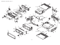
MECHANICAL EXPLODED VIEW 1 / 1
43
B
A
P.C.B
29
10
CDC02AW1
A
D
27
D
26
25
LCD951
9
24
8
44
11
7
27
6
12
45
28
23
P.C.B
D
38
22
1
D
41
D
2
19
18
17
3
D
21
D
F
P.C.B
20
G
D
47
4
15
5
D
16
E
39
42
40
13
D
14
46
B
D
33
P.C.B
34
C
30
H
35
B
37
D
SHEET,PWB
D
B
36
C
32
49
31
– 30 –
48
PANEL,
HT-SINK-AC
MECHANICAL PARTS LIST 1 / 1
REF. NO. PART NO.
31
32
33
34
35
8Z-KC2-203-210
8Z-KC2-221-110
8Z-KC2-011-210
8A-KCF-220-010
8Z-KT1-231-110
KANRI
DESCRIPTION
NO.
LEVER,DFP HOOK -C2
SPR-C,DETACH HOOK-C2
CABI,BASE -C2
COVER, DUST DFP -AC
HLDR,HALF-C
WINDOW,SIDE L -AC15
CABI,FRONT -AC15
BTN,CLEAR S -AC
HLDR,BTN L-AC
LENS,ENCO -AC15
36
37
38
39
40
8Z-KC2-204-210
8Z-KC2-222-010
8Z-KC1-213-010
8A-KC7-230-010
8Z-KC2-201-210
LEVER,DFP LOCK -C2
SPR-T,DETACH LOCK-C2
CHAS,SIDE L -C
HLDR,TR2 -AC
CHAS,FRONT -C2
8A-KCF-007-010
8A-KC7-007-010
8A-KC7-011-010
8A-KCF-208-010
8A-KC7-013-010
BTN,SEESAW L -AC15
BTN,SEESAW R -AC
BTN,CLEAR L -AC
HLDR,BTN R1 -AC15
BTN,CLEAR ML -AC
41
42
43
44
45
88-KC4-641-010
8A-KC7-255-010
8Z-KC1-211-010
8Z-KC1-216-210
8Z-KC7-201-010
FF-CABLE, 20P 1.0 90MM
SPR-C,WIRE
COVER, TOP -C
HLDR,DECK CDC-01
COVER, ISO BLIND -C
16
17
18
19
20
8A-KCF-210-010
8A-KCF-012-010
8A-KCF-008-010
8A-KCF-010-010
8A-KCF-011-010
HLDR,BTN R3 -AC15
BTN,CLEAR EJ -AC15
BTN,MONO -AC15
BTN,CLEAR S2 -AC15
BTN,DETACH -AC15
46
47
48
49
A
8A-KC7-224-010
8A-KC7-225-010
8Z-KC1-214-010
8Z-KC1-212-010
8Z-KC1-253-010
HLDR,P-IC -AC
HLDR,CD-AC
CHAS,SIDE R -C
COVER, BOTTOM -C
S-SCREW,PT 2*8 BH+ BLK
21
22
23
24
25
8Z-KC2-223-010
8A-KC7-006-010
8A-KCF-212-010
8A-KCF-215-010
8A-KCF-213-010
SPR-C,DETACH -C2
BTN,PRE.-AC
LENS,R -AC15
HLDR,LCD -AC15
LENS,LCD -AC15
B
C
D
E
F
87-B10-216-010
8Z-KC1-251-010
87-251-073-410
88-ZG5-317-010
87-251-100-410
U+2.6-4.0 ZINC BLK (BH M2.6)
S-SCREW,TH2.6-4.0-0.8
SCREW,U+2.6-6
S-SCREW,8ZG5S+2-4 W/O
U+3-16
26
27
28
29
30
8A-KCF-214-010
8Z-KT1-236-010
8A-KC7-611-010
8A-KCF-002-010
8A-KCF-020-010
CASE,LCD LENS -AC15
CAP,LAMP BLU
F-CABLE,3P (AUX)
CABI,REAR -AC15
CABI,TRIM -AC15
G
H
87-B10-259-010
87-432-903-010
UT2+3.0-10.0 W/O SLOT (BH TAP)
WASHER,WTE 2.6
1
2
3
4
5
8A-KC7-010-010
8A-KC7-020-010
8A-KC7-220-010
8A-KCF-003-010
8A-KCF-022-010
6
7
8
9
10
8A-KCF-021-010
8A-KCF-001-010
8A-KC7-014-010
8A-KC7-208-010
8A-KCF-211-010
11
12
13
14
15
KANRI
DESCRIPTION
NO.
KNOB,RTRY RUBBER -AC
RING,RTRY -AC
SPR-C,ROTARY -AC
WINDOW,LCD -AC15
WINDOW,SIDE R -AC15
REF. NO. PART NO.
COLOR NAME TABLE
Basic color symbol
Color
Basic color symbol
Color
Basic color symbol
Color
B
Black
C
Cream
D
Orange
G
Green
H
Gray
L
Blue
LT
Transparent Blue
N
Gold
P
Pink
R
Red
S
Silver
ST
Titan Silver
T
Brown
V
Violet
W
White
WT
Transparent White
Y
Yellow
YT
Transparent Yellow
LM
Metallic Blue
LL
Light Blue
GT
Transparent Green
LD
Dark Blue
DT
Transparent Orange
GM
Metallic Green
YM
Metallic Yellow
DM
Metallic Orange
– 31 –
CD MECHANISM EXPLODED VIEW 1 / 1
1
A
A
2
TABLE,DISC
3
4
B
B
5
12
8
6
13
PICK BASE ASSY
14
7
55
9
16
7
55
10
19
SENSOR,
P.C.B
15
20
21
MOTOR
SPINDLE
RF-400CA
11
23
C
24
26
CORD 3P
25
27
LEAD MOTOR A
LEAD MOTOR B
36
38
30
37
33
52
42
41
32
34
51
56
31
43
40
A
A
41
39
D
35
17
44
18
18
22
17
28
54
29
53
46
47
47
A
F
A
49
50
LEAD 2P
– 32 –
48
45
CD MECHANISM PARTS LIST 1 / 1
REF. NO. PART NO.
KANRI
DESCRIPTION
NO.
COVER TOP
LEVER RELEASE
ARM START SET
LEVER,SENSOR
SP LEVER SENSOR
REF. NO. PART NO.
KANRI
DESCRIPTION
NO.
LEVER,R
GEAR H CAM
SP SUB DAMPER
ARM,R
LEVER,LOCK
36
37
38
39
40
S1-100-520-170
S1-100-520-140
S1-100-540-080
S1-100-510-080
S1-100-520-180
DISC ARM L
ROLLER ARM DISC
SP ARM DISC
DISC ARM R
SW,LOAD MPU10853MLB2
41
42
43
44
45
S1-100-540-030
S1-100-520-130
S1-100-520-120
SX-100-710-030
S1-100-520-160
DAMPER SP
GEAR LOAD
GEAR L H
CHASSIS ASSY
LEVER,KICK
S1-100-520-230
S1-100-510-070
S1-100-520-040
S1-100-740-020
S1-100-510-030
GUIDE TOP
PLATE CLAMPER
CLAMPER
SP,ARM CHUCK(L)
ARM CHUCK
46
47
48
49
50
S1-100-520-270
S1-100-760-010
S1-100-510-060
S1-100-520-200
S1-100-770-080
LEVER,SUB KICK
DAMPER ASSY
BRACKET,L M
MOTOR WORM
MOTOR LOAD
16
17
18
19
20
S1-100-740-040
S2-181-600-50D
S1-100-750-020
S1-100-570-070
S1-100-570-140
SP ARM CHUCK(R)
PSW,1.6-5-0.25 (CUT)
LOLLER LOADING
SW,LNNER
LEAD SW A
51
52
53
54
55
S1-100-540-090
S1-100-520-030
S1-100-520-250
S1-100-520-210
S1-100-530-250
SP GEAR SUB
GEAR SUB CAM
LEVER,SW
GEAR,ROLLER
PIN ARM DISC
21
22
23
24
25
S1-100-570-150
S1-100-530-060
S1-100-740-010
S1-100-510-110
S1-100-720-040
LEAD SW B
SHAFT ROLLER
SP FEED
GUIDE,SPG
GUIDE A
56
A
B
C
D
S1-100-520-020
S1-100-550-030
S2-101-170-22P
S2-103-170-60P
S2-103-200-40P
GEAR CAM
SCREW,XP
(+)P. PRECISION SCREW M1.7-2.2
(+)P. PRECISION SCREW M1.7-6
(+)P.PRECISION SCREW M2.0-4.0
26
27
28
29
30
S1-100-570-790
S1-100-770-090
S1-100-540-100
S1-100-520-240
S1-100-270-030
FLEX PICK(FOC)
PICK KSS-710A
SP LEVER UP
LEVER,UP
MOTOR,MAIN FF-030PK
F
S2-101-200-25P
(+)P.PRECISION SCREW M2.0-2.5
31
32
33
34
35
S1-100-520-110
S1-100-520-190
S1-100-730-010
S1-100-520-090
S1-100-520-300
GEAR MOTOR FEED
CASE,MOTOR
SCREW,FEED
GEAR,FEED A
GEAR FEED B
1
2
3
4
5
S1-100-510-130
S1-100-510-090
S1-100-510-180
S1-100-520-220
S1-100-540-070
6
7
8
9
10
S1-100-520-050
S1-100-530-260
S1-100-540-040
S1-100-520-060
S1-100-570-760
11
12
13
14
15
– 33 –
2–11, IKENOHATA 1–CHOME, TAITO-KU, TOKYO 110, JAPAN TEL:03 (3827) 3111
9420025 0251431
Printed in Singapore