1
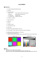
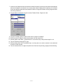
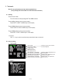
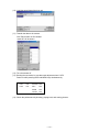
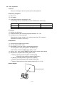
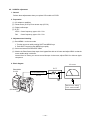
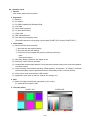
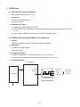
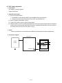
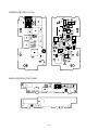
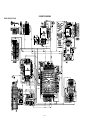
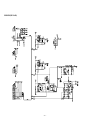
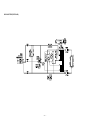
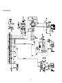
(without price)
QV-2400UX
(KX-785)
JUN. 2001
INDEX
R
CONTENTS
SPECIFICATIONS ....................................................................................................................................... 1
BLOCK DIAGRAM ...................................................................................................................................... 3
ADJUSTMENT ............................................................................................................................................ 4
■ Preparation .......................................................................................................................................... 4
1. PROGRAM LOADING .......................................................................................................................... 5
1-1. Important notice ............................................................................................................................ 5
1-2. To load the program ..................................................................................................................... 5
2. Program version upgrading .............................................................................................................. 7
2-1. How to confirm the program (graphic menu) version .............................................................. 7
2-2. Upgrading using CF card ............................................................................................................ 8
3. Test mode ........................................................................................................................................... 9
3-1. Booting ......................................................................................................................................... 9
3-2. Item for testing ............................................................................................................................. 9
4. Adjustment ....................................................................................................................................... 11
4-1. Color adjustment data writing .................................................................................................. 11
4-1-1. Note ...................................................................................................................................... 11
4-1-2. The example which must be adjusted .............................................................................. 11
4-1-3. To replace the lens ass'y ................................................................................................... 11
4-1-4. To replace CMD-PCB .......................................................................................................... 13
4-2. Flash adjustment ....................................................................................................................... 15
4-3. Flash operation and recharge operation ................................................................................. 16
4-4. Current consumption ................................................................................................................ 17
4-5. VCOM DC adjustment ................................................................................................................ 18
4-6. Operation check ......................................................................................................................... 20
5. D-PCB Assy ...................................................................................................................................... 21
5-1. VCO free run frequency adjustment ........................................................................... 21
5-2. VCOM AC adjustment and VCOM DC coarse adjustment ........................................ 21
5-3. RGB AMP and Sub-Brightness voltage setting adjustment ..................................... 22
5-4. Contrast and Brightness voltage setting adjustment ............................................... 23
5-5. TINT setting adjustment ............................................................................................... 24
6. PW-PCB Assy ................................................................................................................................... 25
6-1. VCC3, VCC3-MD, VCC5, VCC7.5, EVCC3 Voltage check .......................................... 25
6-2. VCC15, VEE7.5 Adjustment ......................................................................................... 25
DISASSEMBLY/ASSEMBLY .................................................................................................................... 26
EXPLODED VIEW ..................................................................................................................................... 36
PARTS LIST .............................................................................................................................................. 37
PRINTED CIRCUIT BOARDS ................................................................................................................... 40
SCHEMATIC DIAGRAMS ......................................................................................................................... 45
SPECIFICATIONS
File Format
Still images (including panoramas): JPEG (Exif. Ver. 2.1) / TIFF, DCF standard (Design rule for
Camera File system), DPOF compatible Movies: AVI (Motion JPEG)
Recording Medium
CompactFlash card (Type I/II), IBM Microdrive
Recorded Image Size
1600 x 1200 pixels, 800 x 600 pixels
Standard Memory Capacity, Number of Image Files, Computer Output Image Size
Still
Number of images
Image size
(pixels)
Quality
1600
x
FINE
NORMAL
1200
800
x
600
File size
8MB
340MB
Compact Flash card
Microdrive
850KB/image
600KB/image
8 images
11 images
401 images
562 images
ECONOMY
350KB/image
19 images
943 images
FINE
NORMAL
200KB/image
150KB/image
33 images
43 images
1587 images
2054 images
ECONOMY
120KB/image
53 images
2494 images
Storage Capacity
Movie (320 x 240 pixels)
Approximately 300KB/second
Recording Time
16 seconds per movie
• The above figures are approximations only.
Image Deletion
Single image; all images in a folder; all images in memory (with image protection)
Imaging Element
1/2.7-inch CCD (Total Pixels: 2.11 million, Effective Pixels; 2.02 million)
Lens
QV-2400UX : F2.8 to 4.5; f = 6.2 to 18.6mm (equivalent to 41 to 123mm lens for 35mm film)
QV-2900UX : F3.2 to 3.5; f = 6 to 48mm (equivalent to 40 to 320mm lens for 35mm film)
Zoom
QV-2400UX : Optical zoom: 3X
Digital zoom: 12X
(in combination with optical zoom)
QV-2900UX : Optical zoom: 8X
Digital zoom: 32X
(in combination with optical zoom)
Image size is 800 x 600 pixels when 4X digital zoom is used.
Focusing
Contrast-detect Auto Focus; manual focus with macro mode and focus lock
Focus Range
QV-2400UX : Normal focus: 10cm to ∞ (1X zoom)
50cm to ∞ (3X zoom)
Macro focus: 1cm to 50cm (1X zoom)
Manual focus: 1cm to ∞ (1X zoom)
50cm to ∞ (3X zoom)
QV-2900UX : Normal focus: 40cm to ∞ (1X zoom)
1m to ∞ (8X zoom)
Macro focus: 1cm to 50cm (1 to 1.6X zoom)
Manual focus: 1cm to ∞ (1X zoom)
1m to ∞ (8X zoom)
The focusing range is the distance from the lens surface to the subject.
Exposure Control
Light Metering: Multi-pattern, center point, spot by CCD
Exposure:
Program AE, Aperture priority AE, Shutter priority AE
Exposure
Compensation: –2EV to +2EV (1/3EV units)
Shutter
CCD electronic shutter; mechanical shutter, BULB, 60 to 1/2000 second
Aperture
QV-2400UX : F2.8, F5.6, auto switching or manual switching
QV-2900UX : F3.2, F4.8, F8, auto switching or manual switching
—1—
White Balance
Automatic, fixed (4 modes), manual switching
Self-timer
10 seconds, 2 seconds
Built-in Flash
Flash Modes: AUTO, OFF, ON, Red eye reduction
Flash Range: QV-2400UX : Approximately 0.5 to 2 meters
QV-2900UX : Approximately 0.5 to 2.5 meters
Recording Functions
Normal, movie, panorama, landscape, night scene, portrait, self-timer, macro, Best Shot, Interval
Monitor
1.8" TFT, low-glare color HAST LCD (122,100 pixels, 555 x 220)
Viewfinder
LCD Monitor or optical viewfinder
Clock
Built-in quartz digital timepiece for time and date recording and storage with image data; auto
calendar up to 2049
Input/Output Terminals
DIGITAL IN/OUT, USB port (special mini port), AC adaptor connector, VIDEO OUT (NTSC,
PAL), External flash sync terminal (QV-2900UX)
Power Supply
Four AA-size alkaline or lithium batteries
Four AA-size nickel-metal hydride rechargeable batteries (NP-H3)
AC adaptor (AD-C620)
AC adaptor charger (BC-3HA)
Battery Life
The values noted below indicate the number of hours before battery failure under normal operating
temperature (25°C). These values are for reference only, and do not guarantee that any particular
set of batteries actually will provide the service life indicated. Low temperatures shorten battery
life.
Type of Operation
Continuous Playback
Continuous Recording
AA-size Alkaline
Batteries LR6
170 minutes
80 minutes
(480 shots)
AA-size Lithium
Batteries FR6
300 minutes
200 minutes
(1200 shots)
AA-size Ni-MH
180 minutes
Batteries NP-H3
120 minutes
(720 shots)
• The above figures are approximations only.
• The above guidelines are based on the following battery types:
Alkaline: MX1500 (AA) DURACELL ULTRA
Lithium: Energizer
• Battery life varies with brand.
Continuous recording values show the number of shots without using the flash. The number of
shots depends on use of the flash and whether flash is turned on or off.
Power Consumption
QV-2400UX : Approximately 5.3W
QV-2900UX : Approximately 5.8W
Dimensions
QV-2400UX : 118(W) x 67(H) x 54(D) mm
QV-2900UX : 121(W) x 80.5(H) x 66(D) mm
Weight
QV-2400UX : Approximately 245g
QV-2900UX : Approximately 295g
(excluding batteries)
Standard Accessories
8MB CompactFlash memory card, Strap; lens cap; cap holder; soft case (QV-2400UX); special
USB cable; special video cable; data transfer cable; CD-ROM; four LR6 alkaline batteries; Basic
Reference, Bundled Software User’s Manual; Best Shot scene List
• This camera does not have a separate battery to power its clock. Clock settings are cleared whenever power to the camera is cut
off (by batteries going dead while the camera is not connected to an AC power outlet with the AC adaptor) for about 24 hours. After
power is resumed, either by loading fresh batteries or connecting to an AC power outlet, you will have to set the correct time and
date again.
• The liquid crystal panel built into this camera is the product of precision engineering, with a pixel yield of 99.99%. This also means,
however that 0.01% of the pixels can be expected to fail to light or to remain lit at all times.
—2—
BLOCK DIAGRAM
R G
LED
FLASH,MACRO,TIMER,
LED,SHIFT
KB-PCB
6pin
C-FPC
CMD-PCB
AD9803
3.3V
ICX284AQ
22pin
CDSSEN
CDSSCK
CDSSDATA
TGSEN
TGSCK
TGSDATA
TGCLK1
TGCLK2
PBLK
RESETB
CDS+AGC+ADC
CCD
(2Mpix)
CXD2470R
36.0MHz
TG
15.0V
-7.5V
PI
D0
D1
D2
D3
D4
D5
D6
D7
D8
D9
CSUBN
HD
VD
VCC15 x 2
VEE7.5 x 2
VCC3 x 5
CGND x 8
3.3V
SDRAM(64Mbit)
CF Controller
uPD65839GC
CPU
4.0MHz
29.5MHz
8bit Micro
computer
D780034AGK
AF
driver
Konica
CL-UNIT
x3 zoom
IRIS
driver
5.0MHz
SHUTTER
driver
MSRDY
MINT
MSCK
MSO
MSI
RESETB
MACT
3.3V
26pin
LCD_DR
VCM7018
VDD:3.3V
VGH:15.0V
VSH:5.0V
SERIAL
USB
24.5454MHz
REC/PLAY
SW
CT1
VCC3 x 2
PON1 VCC5 x 3
(VPP) MGND x 4
(P34)
(P35)
(P36)
3.58MHz
CHROMA
IR3Y29BM
RGB
22pin
CF
LCD Module
3.3V
ZOOM
driver
PI
VIDEO
BR93LC66FV
M
5.0V
7.5V
24.0MHz
EEPROM
(4Kbit)
3.3V
TC74AC367FT x 2
LR38663
22pin
Detection SW
3.3V
3.3V
4-bit
Microprocessor
CF
DET
ADR
BUFFER
3.3V
Operational
Amplifier
5.0V
7.5V
GND VCC3 VCC5
D-PCB
40pin
7pin
KA-PCB
16pin
5.0V
GND
VCC3-M
PW-PCB
M M M
UP
Connerter
Battery
voltage
GND
Xe Lamp
Trigger
Coil
VCC3-MD
GND
VCC1-ST
14pin
Main
Capacitor
IGBT
CHGN
CENDN
LEVELN
SCR
IGBTN
LTTRGN
PREN
F48N
PWM
VCC5 x 2
SGND x 3
JK-PCB
VCC-BL(5.4V)
MAX
685
UP
Connerter
REG
USB
SERIAL
RTC-4574JE
VCC15(15.0V)
RTC
VEE7.5(-7.5V)
VIDEO
AMP
TK15405MTL
DOWN
Connerter
ST-PCB
USB
TRANS
PW,SHUT,MENU,
+,-,TELE,WIDE
PDIUSBP11APW
VCC5(5.0V)
BACK UP
Capacitor
VCC7.5(7.5V)
EVCC3(3.3V)
3pin
Dimmer
Photo
Sensor
Detection
SW (RDET)
GND VCC3 VCC5
DOWN
Connerter
35pin
VCC3(3.3V)
DOWN
Connerter
VCC3-MD(3.3V)
VCC-BL
BLGND
BLSW
BL UNIT
VIDEO
BUZZER
Charging
Booster
AC ADP
—3—
M
3.3V
5.0V
15.0V
-7.5V
80pin
3.3V
FLASH/MASK ROM
(16Mbit)
ADJUSTMENT
■ Preparation
1. PC (IBM Compatible)/OS:Windows 95/98
2. Link cable.
3. Adjustment program
1) adj715.exe
2) fload.exe
3) _romxxxx.bin
4) _gmenuxxxx.bin
(Color adjustment data transfer program)
(Data transfer program for PC)
(Program data)
(Graphic menu data)
4. AC adaptor or stabilizer
5. Digital oscilloscope
6. Multimeter
7. Ammeter
8. Frequency counter
9. TV (with video terminal)
10. Video cable
11. Battery (battery operation/battery cover lock)
12. PC link program : Photo Loader (Communication function confirmation)
13. USB cable/USB driver (USB function confirmation)
14. Test chart (for photography check)
That which carried out color printing of picture data "CHART1.JPG" and the "CHART2.JPG".
CHART1.JPG
CHART2.JPG
■ Notes
Normally power is supplied using AC adaptor.
When error occurs, use a voltage regulator, and supply the specified power.
Make sure to confirm video output specifications (NTSC or PAL) after exchanging the CMD-PCB.
—4—
1. PROGRAM LOADING
1-1. Important notice
Flash ROM on the D PCB contains camera’s operating program and graphic menu. The D PCB is used in
the models QV-2400UX and QV-2900UX however, the programs are different. Therefore, the PCB provided
as a spare part cannot be discriminated which program is recorded.
(Or old program may be recorded.)
Be sure to load the program after you replace the D PCB.
Moreover, when you fail in raising the version of a program with CF card, a program breaks and a camera
cannot be powered, please perform this method for loading program.
(You can upgrade the program by this loading method.)
Note: If QV-2900UX program is loaded in QV-2400UX, display indicates “NOT717 MOTOR” and the camera
does not function.
1-2. To load the program
1. Turn the camera off and remove the CF card then close the CF cover. Disconnect the power source.
2. Connect the PC link cable.
3. Boot transferring program fload.exe. At this time, leave the camera’s power off.
4. Choose the program data “_romXXXX.bin.”
Notes:
*XXXX is 4-digit number depending upon the program version.
*When loading file is chosen, “loaded XXXXXX bytes” is indicated on Status screen.
5. Choose the transfer speed 115K, 57K or 38K. If an error occurs, choose slow transfer speed.
6. Click Progress button on the fload.exe.
—5—
7. Connect an AC adaptor and turn the camera on within 5 seconds. Camera may be turned on automatically
when an AC adaptor is connected. If not, use the power switch. Display shows “read time out” on Status
screen and program data cannot be loaded if it takes too long time between clicking Progress button
and turning camera on.
8. Program data is transferred. Program executes Transfer, Erase, Program in order.
9.
10.
11.
12.
13.
Program is loaded properly if Status screen shows “program completed”.
Disconnect the AC adaptor. (Power switch cannot turn the camera off.)
Choose graphic menu data “_gmenuXXXX.bin” on the above step 4 and perform steps 5 to 10.
Turn the camera off and insert CF card.
While pressing down SHIFT and MENU keys, turn the power on to set the camera in test mode and
check the version number.
14. Turn the camera off then on again and perform the final check by shooting, playing back and erasing.
—6—
2. Program version upgrading
Please check the version and update it if the version is not updated.
Note: Be sure to use AC adaptor.
2-1. How to confirm the program (graphic menu) version
1.
2.
Boot the test mode.
Turn the power on while pushing SHIFT and MENU keys.
Check the LCD display.
(Example)
TEST MODE
PROG
01.
04.
16.
10.
51
r Program version
GMENU
01.
04.
06.
10.
39
r Graphic menu version
····
(Latest version as of May 14, 2001.)
—7—
2-2 Upgrading using CF card
1. Copy the latest upgrade program (_romXXXX.bin) and graphic menu (_gmenuXXXX.bin) on CF card’s
root directory and set the CF card in the camera.
2. Connect an AC adaptor to the camera.
3. Set the camera in PLAY mode and turn the power on while pushing MENU key.
The following screen will be shown.
This time “VER1.000” will be shown.
4. Press [ + ] key to select “YES” and push the shutter button.
The following screen will be shown and loading starts.
5. After about 1 minute, display shows “COMPLETE!” and camera is set in the PLAY mode.
6. Turn the camera off and change CF card to the one for shootings.
7. Set the camera in the test mode by turning power on while pushing down SHIFT and MENU keys and
check the version number.
8. Turn the power off then on again and perform the final check by shooting, playing back and erasing.
—8—
3. Test mode
Note: Do not perform the menu item unless explained here.
(It may damage the internal data and camera becomes unusable.)
3-1. Booting
To boot the test mode;
Turn the camera on while pressing SHIFT and MENU buttons.
To boot MENU1 (Must be done in the test mode)
Press SHIFT ➜ SHIFT ➜ MENU keys in order rapidly.
To boot MENU2 (Must be done in the test mode)
Press FLASH ➜ FLASH ➜ MENU keys in order rapidly.
To boot MENU3 (Must be done in the test mode)
Press SELF ➜ SELF ➜ MENU keys in order rapidly.
* To execute
Use + or – keys to select a test item then press shutter button to execute it.
3-2. Item for testing
1 TEST MODE
• TEST MODE
• PROGRAM Version
• Graphic Menu Version
• Loader Version
• Motor MCU Version
• Power MCU Version
• CCD ADJUST 1 (Yes/No/NG)
• CCD ADJUST 2 (Yes/No/NG)
• STROBE ADJUST (Yes/No/NG)
• KIZU ADJUST (Yes/No/NG)
• ZOOM ADJUST (Yes/No/NG)
• FOCUS ADJUST (Yes/No/NG)
2 MENU1
—9—
Indicates in green-color if all items
have been adjusted.
Indicates "YES" if adjustments have
been completed.
Indicates "NO" if adjustments have
not been proceeded.
Indicates "NG" if an adjustments
failure occurred.
3 MENU2
4 MENU3
— 10 —
4. Adjustment
4-1. Color adjustment data writing
4-1-1. Note
(1) Set of lens ass’y adjusted in the factory and a floppy disc containing the lens’ adjustment data are
provided as a spare part.
(2) These adjustment data are stored in the EEPROM on CMD-PCB.
(3) Help command on adjustment window cannot be used as it uses Japanese system.
4-1-2. The example which must be adjusted
It is necessary to write color adjustment data for the replacements of the following units.
(1) Lens ass'y : [4-1-3]
(2) CMD-PCB : [4-1-4]
4-1-3. To replace the lens ass'y
(1)
(2)
(3)
(4)
Replace the lens ass’y.
Connect an AC adaptor and PC link cable to the camera.
Turn the camera on to set it on PLAY mode.
Boot adjustment program adj715.exe.
At this time, each adjustment data are 0.
— 11 —
(5). Insert the adjustment data floppy disc which comes with the lens ass’y in a PC and load the adjustment
data.
File (F) -> Open (O)
Select floppy disc drive
Select adjustment data which has extension “adj” and load it. If there is no extension “adj”, the file will
not be shown. In such a case, put the extension utilizing windows’ explorer.
Adjustment data file name; 715XXXXX.adj
(XXXXX; 5-digit serial number)
* This number is printed on a seal stuck on the side of the lens unit.
(6). Transfer the adjustment data to the camera.
Click Trans button on the adjustment program.
Send OK will be shown.
(7). Turn the camera on.
(8). While pushing SHIFT and MENU keys, turn the power on to set the camera in the test mode and make
sure that all the adjustment items are "YES".
CCD1
YES
STROBE YES
CCD2
YES
KIZU
YES
ZOOM
YES
FOCUS
YES
(9). Check the performance by shooting, playing back, and erasing pictures.
(10). Perform the flash adjustment (important).
— 12 —
4-1-4. To replace CMD-PCB
(1) Connect AC adaptor and PC link cable to the camera.
Note: Connect the link cable to serial port COM1.
(2) Turn the camera on to set it on PLAY mode.
(3) Boot adjustment program adj715.exe.
At this time, each adjustment data are 0.
(4) Read the adjustment data of before repairs.
Click the Receipt button. "receive OK" will be indicated and adjustment data are shown.
(5) Save the adjustment data in the PC.
File (F) -> Save as (A)
Select a drive to save data.
Name a file name then save the data.
(It is better to name the camera's serial number as the file name.)
XXXXXXXX.ADJ (Note: do not forget the extension code .ADJ.)
(6) Replace the CMD-PCB.
(7) Connect AC adaptor and PC link cable to the camera.
(8) Turn the camera on and set it on PLAY mode.
(9) Boot the adjustment program (adj715.exe).
— 13 —
(10) Load the saved data of the lens unit.
(11) Transfer the data to the camera.
Click Trans button on ADJ window.
“send OK” will be shown.
(12) Turn the camera off.
(13) Booting the test mode, be sure that each adjustment item is YES.
Power on while pressing DISP and MENU keys simultaneously.
CCD1
YES
STROBE YES
CCD2
YES
KIZU
YES
ZOOM
YES
FOCUS
YES
(14) Check the performance by shooting, playing back, and erasing pictures.
— 14 —
4-2. Flash adjustment
1. General
When you exchange a flash unit, please perform this adjustment.
2. Necessary equipment
(1) Dark room
(2) AC adaptor
(3) Gray paper (Superior's oxford gray No. 22)
The following sizes are available from us (also available from camra shop).
Parts code
1904 5411
1904 5412
Parts name
Superior photographing background paper
Sperior photographing background paper
Specifications
No. 22 (1.75 x 2.7m)
No. 22 (2.72 x 11m)
3. Condition
(1) Perform in a dark room.
(2) Distance between flash lens and gray paper should be 70 ± 5 cm.
(3) Use lighter color of the gray paper.
Paper should be larger enough to fit in a picture taken from 70 cm distance.
(Reference; more than 1.5m x 2.0m)
4. Adjustment
(1) Connect an AC adaptor to the camera.
(2) Set the camera in REC mode.
(3) Boot MENU 2 in the test mode by the following operations;
Turn the power on while pushing SHIFT and MENU keys.
Push FLASH, FLASH, and MENU keys rapidly in order.
(4) Using + and – keys, select STROBE ADJ and push the shutter release button.
(5) Adjustment is completed after emitting flash 5 times.
1st flashing; Checking amount of light in normal shooting
(Emitting 4 times maximum changing PWM value.)
nd
2 flashing; Confirming amount of light of the 1st flashing.
3rd flashing; Checking brightness after changing PWM value.
4th flashing; Checking the circuit for changing aperture (F2.8 -> F5.6).
5. Block diagram
Back ground paper.
70 cm
POWER
ON/OFF
W
MENU
T
REC
PLA
Y
RD
CA
SHIFT
INFO
MF
IZE
RES
QV-2400UX
— 15 —
4-3. Flash operation and recharge operation
1. General
When you exchange a flash unit, please perform this adjustment.
2. Necessary equipment
(1) Dark room
(2) AC adaptor
(3) Gray paper (Superior's oxford gray No. 22)
The following sizes are available from us (also available from camra shop).
Parts code
1904 5411
1904 5412
Parts name
Superior photographing background paper
Sperior photographing background paper
Specifications
No. 22 (1.75 x 2.7m)
No. 22 (2.72 x 11m)
3. Condition
(1) Perform in a dark room.
(2) Distance between flash lens and gray paper should be 70 ± 5 cm.
(3) Use lighter color of the gray paper.
Paper should be larger enough to fit in a picture taken from 70 cm distance.
(Reference; more than 1.5m x 2.0m)
4. Adjustment
(1)
(2)
(3)
(4)
Connect an AC adaptor to the camera.
Set the camera in red-eye reduction mode.
Shoot a back ground paper (confirm pre-flashing and actual flashing.)
Connect the camera and TV’s video terminal with a video cable and check the picture.
Should not be too white, too dark, or colored.
(5) Flash charging current should not exceed 1.3 A.
(6) Shoot in non-flash mode and confirm flash does not emit light.
5. Block diagram
Video cable
QV-2400UX
TV monitor
(with a video input terminal)
Back ground paper
— 16 —
4-4. Current consumption
1. General
When consumption of a battery is early, check.
2. Conditions
• Set QV-2400UX to “PLAY” mode.
3. Preparation
(1) Voltage regulator.
(2) Ammeter.
4. Adjustment procedure
(1) Current consumption (DC in = 6.0 ± 0.1 [V])
• Make sure that current consumption is less than 500 mA in PLAY mode.
• Make sure that current consumption is less than 650 mA in REC mode.
(Flash charge current is not included)
(2) Lower the voltage from 6 V as shown below then make sure the battery warning indicator changes.
DC in = 5.0 ± 0.05 [V] (one indicator is off )
DC in = 4.65 ± 0.05 [V] (two indicators are off)
DC in = 4.35 ± 0.05 [V] (All the indicators are off)
— 17 —
4-5. VCOM DC adjustment
1. General
Perform these adjustments when you replace LCD module or D-PCB.
2. Preparation
(1)
(2)
(3)
(3)
AC adaptor or stabilizer.
Photo sensor (S1153)/ Photo sensor amp (C2719)
Digital oscilloscope.
B. P. F
NTSC: Center frequency; approx. 60 ± 5 Hz
Center frequency; approx. 50 ± 5 Hz
PAL:
3. Adjustment and checking
(1) Boot MENU 1 on the test mode.
1. Turn the camera on while pushing SHIFT and MENU keys.
2. Push SHIFT keys twice then MENU keys rapidly.
(2) Select and execute 50 PERCENT GRAY.
(3) Monitor the Photo Sensor Amp output via a bypass filter with an AC meter and adjust VR321 so that the
meter needle swing is minimum.
Instead of an AC meter, you can use an oscilloscope. In that case, adjust VR321 for minimum ripple
component.
4. Block diagram
AC meter
B.P.F
Photo diode
S1153
Photo Sensor Amp
C2719
POWER
ON/OFF
W
MENU
T
REC
PLA
Y
RD
Minimize the swing
of AC meter needle.
CA
SHIF
T
INFO
QV-2400UX
LCD
MF
IZE
RES
— 18 —
Note: Easy adjustment
(1) Boot MENU 1 on the test mode.
1. Turn the camera on while pushing SHIFT and MENU keys.
2. Push SHIFT keys twice then MENU keys rapidly.
(2) Select and execute GRAY SCALE (10 STEP).
(3) Adjust VR321 for distinctive 10 gray steps.
— 19 —
4-6. Operation check
1. General
After repairs, please check if needed.
2. Preparation
(1) Batteries.
(2) AC adaptor.
(3) PC (IBM compatible)/OS:Windows 95/98.
(4) Link cable.
(5) Photo loader (program).
(6) TV (with video teminal).
(7) Video cable.
(8) USB cable/USB driver
(9) Test chart (for photography check)
(That which carried out color printing of picture data "CHART1.JPG" and the "CHART2.JPG".)
3. Check matter
(1) Shock and flash check (essential)
1 Shoot the test chart without flashing.
2 Shoot the test chart with flashing.
3 Confirm the result (compare with properly functioning camera) for;
• Color
• Focus and resolution
(2) Unti-shock, Battery operations, AC Adaptor check
(3) Power jack, switch, buttons operations
(4) CompactFlash insersion/eject operation, Cover open/close operation, battery cover open/close operation.
Lens block rotation
(5) Image reversing, Normal/Macro switching, ZOOM operation, AE operation , AF operation, Self-timer
count down display, exposure adjustment function, flash display function, self-timer function.
(6) Video output, serial communication, USB function.
(7) Appearance check (Dust on the lens, scratch, dirt, damage, etc.)
4. Note
(1) Make sure Video out setting are appropriate to your country.
(i.e. Japan=NTSC, England = PAL)
5. Test chart picture
CHART1.JPG
CHART2.JPG
— 20 —
5. D-PCB Assy
5-1. VCO free run frequency adjustment
Room temperature should be 20 ± 10 °C
1. Preparation
• AC adaptor or voltage regulator
• Frequency counter
2. Adjustment procedure
(1) Connect SYF (CP355) and GND (CP344).
(2) Monitor HDB (CP301) with frequency counter and adjust VR320 so that frequency becomes 15.734 ±
0.1 KHz.
(3) After completing adjustment, disconnect SYF (CP355) and GND (CP344).
5-2. VCOM AC adjustment and VCOM DC coarse adjustment
1. General
Perform these adjustments after D PCB or LCD module is replaced.
2. Preparation
• AC adaptor or voltage regulator
• Digital oscilloscope
3. Adjustment procedure
(1) Make sure amplitude of VCOM output (CP340) is 5.15 ± 0.30 Vp-p.
(2) Adjust VR321 so that maximum VCOM output (CP340) will be 3.60 ± 0.20 V.
4. Connection diagram
QV-2400UX
D-PCB
High level
3.60 [V]
0 [V]
–1.55 [V]
VCOM
(PC340)
Power supply
Oscilloscope
— 21 —
Amplitude
5.15 ± 0.30
[VP-P]
5-3. RGB AMP and Sub-Brightness voltage setting adjustment
1. General
Perform the following adjustments in order.
5-3. RGB AMP and Sub-Brightness voltage setting adjustment
5-4. Contrast and Brightness voltage setting adjustment
5-5. TINT setting adjustment
2. Preparation
• AC adaptor or voltage regulator
• Digital oscilloscope
3. Adjustment procedure
(1) Start up Test mode Menu1.
1. Turn POWER on while pressing SHIFT key and MENU button simultaneously
2. Quickly press keys in the order of SHIFT key, SHIFT key and MENU key.
(2) Select / Execute GRAY SCALE (10 step). (NTSC)
(3) Impress the killer terminal (CP308) with VCC5 (CP520) voltage through a 22 kΩ resistance.
(4) Trigger VG waveform (CP322) by FRP (CP300) signal to adjust as noted below.
(5) Adjust RGB-AMP VR (VR302) so that pedestal-pedestal voltage of VG(CP322) signal is 4.70 ± 0.05
Vp-p.
(6) Adjust SUB R BRIGHT VR (VR305) so that potential between VR (CP320) signal’s pedestal and pedestal
is 4.70 ± 0.05 Vp-p.
(7) Adjust SUB B BRIGHT VR (VR304) so that potential between VB (CP324) signal’s pedestal and pedestal
is 4.55 ± 0.05 Vp-p.
3. Notes
• Consecutively, execute 5-4. Contrast and Brightness voltage setting adjustment.
• Make sure that waveforms are not distorted.
4. Connection diagram
VCC5
QV-2400UX
D-PCB
Power
Supply
22KΩ
Killer terminal
(CP308)
VR(CP320)
VG(CP322)
Digital oscilloscope
VB(CP324)
Figure 1
4.70 ± 0.05 [Vp-p]
(pedestal – pedestal)
pedestal level
Figure 1
— 22 —
5-4. Contrast and Brightness voltage setting adjustment
1. Preparation
• AC adaptor or voltage regulator
• Digital oscilloscope
2. Adjustment procedure
(1) Start up Test mode Menu1.
1. Turn POWER on while pressing SHIFT key and MENU button simultaneously
2. Quickly press keys in the order of SHIFT key, SHIFT key and MENU key.
(2) Select / Execute GRAY SCALE (10 step). (NTSC)
(3) Trigger VG waveform (CP322) by FRP (CP300) signal to adjust as noted below.
(4) Adjust CONTRAST VR (VR306) so that contrast terminal voltage(CP302) signal is 1.50 ± 0.05 V.
(5) Adjust BRIGHT VR (VR303) so that potential between signal’s pedestal and 4 step is 2.25 ± 0.05 Vp-p.
(6) Adjust CONTRAST VR (VR306) so that potential between signal’s pedestal and 10 step is 2.85 ± 0.05
Vp-p.
(7) Remove the resistance set between the killer terminal (CP308) and the VCC5 (CP520).
3. Notes
• Consecutively, execute 5-5. TINT setting adjustment.
• Make sure that waveforms are not distorted.
4. Connection diagram
VCC5
QV-2400UX
22KΩ
D-PCB
Killer terminal
(CP308)
Power
Supply
Digital oscilloscope
VG(CP322)
Figure 2
2.25 ± 0.05 [Vp-p]
(pedestal – 4STEP)
pedestal level
Figure 2
— 23 —
5-5. TINT setting adjustment
1. Preparation
• AC adaptor or voltage regulator
• Digital oscilloscope
2. Adjustment procedure
(1) Start up Test mode Menu1.
1. Turn POWER on while pressing SHIFT key and MENU button simultaneously
2. Quickly press keys in the order of SHIFT key, SHIFT key and MENU key.
(2) Select / Execute COLOR BAR. (NTSC)
(3) Trigger FRP (CP300) signal to adjust as noted below.
(4) Adjust the VR301 in order to set the potential difference of the fourth pulse height B (between a pedestal
and the peak) and the second pulse height A (between a pedestal and the peak) of the four pulses of
the VB wave form (CP324) to be less than 0.1 [Vp-p].
3. Notes
• Perform the adjustment consecutively after RGB AMP, Sub brightness, Brightness adjustments.
4. Connection diagram
QV-2400UX
D-PCB
1 2 3 4
Power
Supply
A
VB(CP324)
— 24 —
B
Digital oscilloscope
6. PW-PCB Assy
6-1. VCC3, VCC3-MD, VCC5, VCC7.5, EVCC3 Voltage check
1. Preparation
• AC adaptor or voltage regulator
• Multimeter
2. Adjustment procedure
Confirm the following voltages.
VCC3 (CP110) = 3.30 ± 0.10 [V]
VCC3 -MD (CP115) = 3.30 ± 0.10 [V]
VCC5 (CP125) = 5.00 ± 0.15 [V]
VCC7.5 (CP130) = 7.50 ± 0.50 [V]
EVCC3 (CP140) = 3.30 ± 0.10 [V]
6-2. VCC15, VEE7.5 Adjustment
1. Preparation
• AC adaptor or voltage regulator
• Multimeter
2. Adjustment procedure
• Adjust VR135 so that VCC15 (CP136) = 15.0 ± 0.10 V.
• Adjust VR136 so that VEE7.5 (CP135) = -7.5 ± 0.10 V.
— 25 —
DISASSEMBLY
4. Open the Case.
1. Remove two screws at the bottom.
5. Remove the connector (CN530).
Screws
2. Rotate the CAM case and unserew one screw
on the side.
6. Remove the connector (CN522).
Screw
3. Rotate the CAM case to the other side and
unscrew one screw on the side.
7. Remove the connector (CN521).
Screw
— 26 —
8. Remove the connector (CN900).
12. Remove two screws affixing the lens block.
Screws
9. Remove the connector (CN101).
13. Remove the connector (CN510).
10. Lift up the bending of solderless terminal.
14. Separated in three blocks.
11. Remove the Screw.
15. Remove the Screw.
— 27 —
16. Remove the JK-PCB.
20. Open the case.
17. Remove the connector (CN800).
21. Remove the upper case.
18. Remove the Battery cover.
22. Remove the connector (CN100).
19. Remove the screw at the bottom.
23. Remove the battery holder.
— 28 —
24. Remove the screw.
28. Remove the screw.
25. Remove the KA-PCB.
29. Remove the D-PCB.
26. Remove two screws.
30. Remove the connector (CN540).
Screws
27. Remove the PW-PCB.
31. Remove three screws.
Screws
— 29 —
32. Remove the Back Light.
33. Remove the LCD.
34. Remove two screws.
Screws
35. Remove the KB-PCB.
— 30 —
LENS BLOCK
1. As you push a hook from a top, fit a driver
over the slot of the lens side.
NOTE: Be careful not scratch the case.
3. Do the same thing on the other side.
4. Open the case from the flash side.
2. Lift the screw driver so that the hook goes
under the case.
5. Remove the Case.
6. Unsolder the lead wire.
— 31 —
8. Unsolder the lead wire.
12. Remove the connector (CN250).
9. Remove the connector (CN761).
13. Remove the connector (CN290).
10. Remove the connector (CN700).
14. Remove three screws.
Screws
11. Remove the connector (CN251).
15. Open tne CMD-PCB.
— 32 —
16. Disconnect the connector CN760 and remove
CMD-PCB.
20. Remove the Lnes block.
17. Remove the screw on Lens block.
21. Discharge flash capacitor by discharging tool.
18. Remove the screw on Lens block.
22. Remove two screws at the other side.
Screws
19. Remove the screw (1.7 x 9 black) on Lens
block.
11. Remove the connector (CN400).
— 33 —
24. Remove the L-case block.
27. It is easier if you push the front of the flash.
25. Remove a screw (1.7 x 5 black).
28. Unhook the other side of the flash unit.
26. Disengage the hook on the flash unit using a
screw driver.
NOTE: Make sure to discharge the capacitor for
the flash fully otherwise it sparks.
29. Open the case and remove the flash unit.
30. After the disassembly
— 34 —
Hints for the assembly
1. Put the cable of a flash unit into the slot on
the case.
2. Also put the other cable into the slot.
Tool
Soldering iron / solder / desoldering wire
precision screwdrivers / Tweezers
Discharge tool (Resistor 1.5 kΩ 5 W)
— 35 —
EXPLODED VIEW
S4
7
S4
28
29
38
30
S12
34
×3
22
35
45
×2
S6
S1
×2
11
37
8
49
6
12
S12 × 2
17
9
S9
32
20
40
15
23
50
S1
×2
5
1
10
S3
36
16
S10
21
×2
S2
S12
53
33
×2
51
S5
19
S3
52
S8
14
44
24
26
S4
×2
4
54
25
43
S12
S5
27
S8
42
2
13
39
47
31
3
18
41
48
S6
46
— 36 —
×2
QV-2400UX
MAIN BODY COMPONENT
N
Item
Code No.
Parts Name
1
1003 4054 BACK LIGHT ASSY
2
1002 8729 CABLE/BACK LIGHT
N
3
1005 5360 COVER/BATTERY
4
1003 4056 HOLDER/BATTERY
N
5
1005 5352 CASE/FRONT/LENS
N
6
1005 5354 LENS BLOCK
N
7
1005 4001 CASE/REAR/LENS
N
8
1005 3987 COVER/CF
9
1002 8714 COVER/LED
10
1003 4795 CABLE/KEY
11
1002 8700 LABEL/COVER/CF
12
1003 4076 LENS&CCD ASSY
13
1005 3988 COVER/CONNECTOR
14
1003 4065 PCB UNIT/DIGITAL
15
1002 8715 SPACER/LCD
16
1003 4068 CASE/LENS UNIT
17
1002 8712 BUTTON/MENU
18
1002 8775 BUTTON/MODE
19
1003 4369 PCB ASSY/KEY(KA)
20
1003 4066 PCB ASSY/KEY(KB)
21
1003 4048 PCB ASSY/BACK LIGHT
22
1003 4071 PCB ASSY/CMD
23
1003 4072 PCB ASSY/STROBE
24
1003 4049 PCB ASSY/JACK
25
1003 4046 PCB ASSY/POWER
26
1002 8724 PLATE/METAL
27
1003 4794 CABLE/POWER
28
1003 4556 SPRING/POWER
N
29
1005 3993 KNOB/POWER
N
30
1005 3991 KNOB/REC
31
1002 8777 SPRING/SHUTTER
32
1002 8706 LCD MODULE/TFT
33
1003 9678 BUZZER
N
34
1005 3992 KNOB/ZOOM
35
1004 2653 SPRING/ZOOM
36
3851 2113 LAMP/FLUORESCENT
N
37
1005 3983 PLAE/RATING
N
38
1005 3990 CASE/UPPER
N
39
1005 5361 PANEL ASSY/UPPER
40
1002 8742 STROBE UNIT
41
6611 0460 PLATE/NAME
42
6400 9740 WASHER
43
1002 8725 CABLE/B-K715
44
1002 8723 CABLE/C-K715
45
1003 0070 TRIPOD NUT
N
46
1005 5358 CASE/LOWER
47
1002 8774 BUTTON/SHUTTER
48
6613 1330 HOOK/STRAP
49
1004 0721 PLATE/SHIELD
50
1003 4799 CABLE
51
1000 1733 CUSHION
52
1003 4797 TAPE/INSULATION
53
1004 0278 PALTE/INSULATION
54
1002 8728 TAPE/ADHESIVE
Notes:
N : New registration parts
Q : Quantity used per unit
R : Rank
Specificaion
K342253*1 TK(K715)
K442243-1
K342255*005V01TK
K342254*1 TK(K715)
K342251*004V01TK
K241468*004V01TK
K241414-004V01
K342115-004V01
K342138-1
K442309-001V02
K441492-4
RJK501421*001V01TK
K342116-005V01
RJK501405*001V01TK
K442235-1
K241465*2 TK(K715)
K342135-1
K342114-1
K241459*2 TK(K715)
K241459*3 TK(K715)
K442325*1 TK(K715)
K140771*1 TK(K715)
K140771*2 TK(K715)
K442328*1 TK(K715)
K442323*1 TK(K715)
K342117-1
K442252-001V02
K442207-001V02
K342134-004V01
K342132-004V02
K442212-1
COD18T1029FN
PKM35-4A44
K342133-004V01
RJK501745-001V01
CAS-1.8JS1.8-1
K442274-005V01
K140742-005V01
K342256*005V01TK
CO-715
C441170-1
A412353-1
K342165-1
K241412-1
K342112-2
RJK501402*005V01 TK
K342113-1
R340181-2
RJK501493-001V03
RJK501530-001V01
K441962-1
RJK501511-001V01
RJK501655-001V02
K442226-1
- 37 -
Applicable
Common
Common
Common
Common
Common
Common
Common
Common
Common
Common
Common
Common
Common
Common
Common
Common
Common
Common
Common
Common
Common
Common
Common
Common
Common
Common
Common
Common
Common
Common
Common
Common
Common
Common
Common
Common
Common
Common
Common
Common
Common
Common
Common
Common
Common
Common
Common
Common
Common
Common
Common
Common
Common
Common
Q Price Code
1
CR
1
AF
1
AX
1
BI
1
CV
1
EK
1
BB
1
AF
1
AB
1
AC
1
AA
1
EG
1
AI
1
EG
1
AA
1
CQ
1
AH
1
AH
1
CF
1
CF
1
CI
1
CZ
1
CZ
1
CX
1
CX
1
AA
1
AJ
1
AA
1
AA
1
AA
1
AA
1
DE
1
AG
1
AA
1
AA
1
AW
1
AA
1
AY
1
CG
1
CE
1
AG
1
AA
1
AG
1
AZ
1
AC
1
CM
1
AG
1
AE
1
AA
1
AA
1
AA
1
AA
1
AA
1
AA
R
A
X
A
X
X
A
X
A
X
X
A
A
B
A
X
X
X
X
B
B
B
A
A
A
A
X
X
X
X
X
X
A
C
X
X
A
X
X
X
A
X
C
X
X
C
X
X
C
X
X
X
X
X
X
N
-
Item
S1
S2
S3
S4
S5
S6
S7
S8
S9
S10
S11
S12
Code No.
1003 6886
1002 8722
1002 8704
1001 2551
1002 8705
5861 4345
1002 8702
5861 3551
1002 8744
1002 8693
1002 5765
1003 6882
ACCESSORY
N
Item
Code No.
N
1005 5570
3816 0259
N
1005 1462
N
1005 5585
N
1005 5586
1014 8773
N
1003 1611
1015 1524
3502 2744
1015 1471
PCB
N
Item
Code No.
BL-PCB
- CN900 3502 2230
Q902 2259 2744
Q903 2259 2789
T900 3012 1624
CMD-PCB
- CN250 3502 2214
- CN251 3502 2214
- CN760 3502 2600
- IC752 2105 6398
- IC753 2105 6398
D-PCB
- CN340 3501 8491
D340 2390 1379
D350 2390 1820
D351 2360 3060
D352 2390 1358
H520 2590 2707
- IC330 2114 5805
- IC521 2105 6486
- IC522 2105 6485
N SW510 1002 1883
- SW520 2254 0555
- VR301 2775 3464
- VR302 2775 3465
- VR303 2775 3464
- VR304 2775 3464
- VR305 2775 3464
- VR306 2775 3465
- VR320 2775 3464
Notes:
N:
Q:
R:
Parts Name
SCREW
SCREW
SCREW
SCREW
SCREW
SCREW
SCREW
SCREW
SCREW
SCREW
SCREW
SCREW
Specificaion
BT3 1.4X3.0 BK
BT3 1.7X12.0BK
BT3 1.7X3.0 BK
BT3 1.7X3.5 BK
BT3 1.7X4.5 BK
PS3 1.7X3.5 NI
PS3 1.7X3.5 BK
M1.7X3.0 BK
M1.7X5.0 BK
BT3 1.7X5.5 BK
BT3 1.7X4.0 BK
BT3 1.7X4.0 NI
Applicable
Common
Common
Common
Common
Common
Common
Common
Common
Common
Common
Common
Common
Q Price Code
3
AA
1
AA
3
AA
7
AA
2
AA
3
AA
0
AA
2
AA
1
AA
2
AA
0
AA
6
AA
R
X
X
X
X
X
X
X
X
X
X
X
X
Parts Name
CD-ROM
BATTERY/ALKALINE
HOLDER/CAP
STRAP
CASE/SOFT
CABLE/VIDEO
CAP/LENS
CARD/CF(8MB)
CABLE/USB
CABLE/PC-LINK
Specificaion
CK785DCA01R
LR6G/2ST
CH-K786
ST-K785
SC-785
VC-K723-FC
LC-K715-A
HB289008C4XA
59204-2301
LC9F-DOS-K740-L
Applicable
Except for US
Except for US
Common
Common
Common
Common
Common
Except for US
Common
Except for US
Q Price Code
1
AK
2
AG
1
AF
1
AG
1
AY
1
AL
1
AG
1
DF
1
BK
1
BU
R
X
X
C
C
C
C
C
X
C
C
Parts Name
Specification
Applicable
Q Price Code R
CONNECTOR
TRANSISTOR/DIGITAL
TRANSISTOR/ARRAY
TRANSFORMER/INVERTER
SM03B-SRSS-TB
DTA143EETL
IMX17T110
BLT1.8K713
Common
Common
Common
Common
1
1
1
1
AC
AA
AA
AT
X
X
X
X
CONNECTOR
CONNECTOR
CONNECTOR
IC
IC
52435-2291
52435-2291
52746-0790
LB1846M-TE-L
LB1846M-TE-L
Common
Common
Common
Common
Common
1
1
1
1
1
AD
AD
AB
AH
AH
X
X
X
X
X
CONNECTOR
DIODE/SCHOTTKY
DIODE/CHIP
DIODE/ZENER CHIP
DIODE/VARICAP
OSCILLATOR/CRYSTAL
IC
IC
IC
SWITCH/SLIDE
SWITCH
RESISTOR/SEMIFIXED CHIP
RESISTOR/SEMIFIXED CHIP
RESISTOR/SEMIFIXED CHIP
RESISTOR/SEMIFIXED CHIP
RESISTOR/SEMIFIXED CHIP
RESISTOR/SEMIFIXED CHIP
RESISTOR/SEMIFIXED CHIP
New registration parts
Quantity used per unit
Rank
52435-2691
MA729-(TX)
1SS355TE-17
MA8100-H(TX)
MA329-(TX)
CSTCC4.00MG-TC
NJM3414AV-TE1
S-80835ANNP-EDZ-T2
S-80830ANNP-EDT-T2
SSSS812-B-2B
ESE22MH4
POZ2AN-1-203N-T00
POZ2AN-1-503N-T00
POZ2AN-1-203N-T00
POZ2AN-1-203N-T00
POZ2AN-1-203N-T00
POZ2AN-1-503N-T00
POZ2AN-1-203N-T00
Common
Common
Common
Common
Common
Common
Common
Common
Common
Common
Common
Common
Common
Common
Common
Common
Common
Common
1
1
1
1
1
1
1
1
1
1
1
1
1
1
1
1
1
1
AE
AB
AA
AA
AC
AC
AI
AB
AB
AB
AC
AA
AA
AA
AA
AA
AA
AA
X
X
X
X
X
X
X
X
X
A
C
X
X
X
X
X
X
X
- 38 -
N
N
N
N
N
N
N
-
Item
JK-PCB
C860
D810
D811
D830
IC800
IC810
IC821
JK800
JK810
JK820
Q424
Q426
Q801
Q810
Q820
Q840
SW850
KA-PCB
SW880
SW881
SW882
SW883
SW884
SW885
SW886
KB-PCB
SW895
SW896
SW897
SW898
PW-PCB
CN100
CN103
D100
FU100
FU101
FU102
FU103
JK100
Q110
Q115
Q120
Q121
Q130
VR135
VR136
ST-PCB
D402
D411
D412
IC420
Q422
Q424
Q425
Notes:
Code No.
Parts Name
Specification
Applicable
Q Price Code R
2845 6624
2390 1379
2390 1379
2390 1477
2105 6490
2105 5712
6571 0037
3025 1937
3501 8197
3502 2717
2259 2731
2259 2731
2259 2715
2795 8150
7911 3830
2259 2745
1002 8209
CAPACITOR/BACK-UP
DIODE/SCHOTTKY
DIODE/SCHOTTKY
DIODE/CHIP
IC
IC
IC/L-MOS
JACK
JACK/MINI
CONNECTOR
TRANSISTOR/DIGITAL
TRANSISTOR/DIGITAL
TRANSISTOR/DIGITAL
FET/CHIP
FET
TRANSISTOR/DIGITAL
SWITCH/SLIDE
EECS0HD104H
MA729-(TX)
MA729-(TX)
MA142WA-(TX)
TK15405MTL
TC7S04FU(TE85L)
TC7W00FU(TE12L)
HSJ1636-011020
HSJ1169-019010
55427-0428
DTA114EE-TL
DTA114EE-TL
DTC144EETL
2SK2035(TE85L)
2SJ347(TE85L)
DTC143EETL
SPVG31-T
Common
Common
Common
Common
Common
Common
Common
Common
Common
Common
Common
Common
Common
Common
Common
Common
Common
1
1
1
1
1
1
1
1
1
1
1
1
1
1
1
1
1
AF
AB
AB
AA
AH
AB
AD
AE
AF
AJ
AA
AA
AA
AA
AA
AA
AB
X
X
X
X
X
X
X
A
A
A
X
X
X
X
X
X
A
1001 4578
3412 1995
3412 1995
3412 1995
2254 0555
2254 0555
2254 0555
SWITCH/TOUCH
SWITCH/TACT
SWITCH/TACT
SWITCH/TACT
SWITCH
SWITCH
SWITCH
TSW-3D-T50
SKQRAA-T
SKQRAA-T
SKQRAA-T
ESE22MH4
ESE22MH4
ESE22MH4
Common
Common
Common
Common
Common
Common
Common
1
1
1
1
1
1
1
AC
AB
AB
AB
AC
AC
AC
A
A
A
A
C
C
C
3412 1995
3412 1995
3412 1995
3412 1995
SWITCH/TACT
SWITCH/TACT
SWITCH/TACT
SWITCH/TACT
SKQRAA-T
SKQRAA-T
SKQRAA-T
SKQRAA-T
Common
Common
Common
Common
1
1
1
1
AB
AB
AB
AB
A
A
A
A
3501 7091
3502 2437
2390 2506
1001 2479
1000 9214
1000 9214
1003 4689
3501 6755
2254 0570
2254 0570
2795 8157
2259 2715
2250 1596
2775 3465
2775 3465
CONNECTOR/PCB
CONNECTOR
DIODE
FUSE/CHIP
FUSE/CHIP
FUSE/CHIP
FUSE/CHIP
JACK/POWER
FET
FET
FET/CHIP
TRANSISTOR/DIGITAL
TRANSISTOR/CHIP
RESISTOR/SEMIFIXED CHIP
RESISTOR/SEMIFIXED CHIP
53254-0310
52745-1690
RB060L-40-TE25
434.750
434001
434001
43401.5
HEC3600-010120
SI2301DS-T1
SI2301DS-T1
CPH6401-TL
DTC144EETL
SI2302DS-T1
POZ2AN-1-503N-T00
POZ2AN-1-503N-T00
Common
Common
Common
Common
Common
Common
Common
Common
Common
Common
Common
Common
Common
Common
Common
1
1
1
1
1
1
1
1
1
1
1
1
1
1
1
AA
AC
AD
AB
AB
AB
AB
AD
AE
AE
AE
AA
AE
AA
AA
X
X
X
A
A
A
A
A
X
X
X
X
X
X
X
2390 3100
2390 3102
2390 3101
2105 4158
2795 8150
7101 5791
2252 0637
DIODE/ZENER
DIODE/ZENER
DIODE/ZENER
COMPARATOR
FET/CHIP
TRANSISTOR/CHIP
TRANSISTOR/CHIP
02DZ13-Y(TPH3)
F1C2300TP
02DZ8.2-Y(TPH3)
TA75S393F(TE85L)
2SK2035(TE85L)
DTA144EETL
2SC4081-T106R
Common
Common
Common
Common
Common
Common
Common
1
1
1
1
1
1
1
AA
AD
AA
AC
AA
AA
AA
X
X
X
X
X
X
X
N : New registration parts
Q : Quantity used per unit
R : Rank
- 39 -
PRINTED CIRCUIT BOARDS
DIGITAL-PCB (PCB 715-D)
— 40 —
POWER-PCB (PCB 715-PW)
BACK LIGHT-PCB (PCB 715-BL)
— 41 —
JACK-PCB (PCB 715-JK)
KA-PCB (PCB 715-KA)
— 42 —
KB-PCB (PCB 715-KB)
CMD-PCB (PCB 715-CMD)
— 43 —
CCD-PCB (PCB 715-CCD)
ST-PCB (PCB 715-ST)
— 44 —
SCHEMATIC DIAGRAMS
DIGITAL-PCB (PCB-715A-D)
— 45 —
POWER-PCB (PCB-715A-PW)
— 46 —
BACK LIGHT-PCB (PCB-715A-BL)
— 47 —
JACK-PCB (PCB-715A-JK)
— 48 —
KEY-PCB (PCB-715A-KA)
— 49 —
KEY-PCB (PCB-715A-KB)
— 50 —
CMD-PCB (PCB-715CMD)
— 51 —
CCD-PCB (PCB-715CCD)
— 52 —
ST-PCB (PCB-715A-ST)
STROBE UNIT
— 53 —
CASIO TECHNO CO.,LTD.
Overseas Service Division
Nishi-Shinjuku Kimuraya Bldg. 1F
5-25, Nishi-Shinjuku 7-Chome
Shinjuku-ku, Tokyo 160-0023, Japan