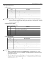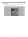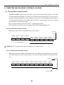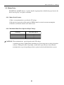
1
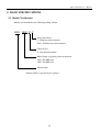
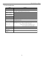
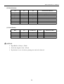
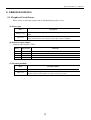
User’s Manual
CONTROL BOARD FOR MLT-388/MLT-389
MODEL BD2-3880/3890
Rev. 1.00 Newly Issued on October 22, 2004
REVISION
Rev. No.
1.00
1.00
Date
2003.06.23
2004.10.22
Content
Issued as first edition.
“3.3 CN3 Connector for Interface” changed
i
CONTENTS
1. OUTLINE ....................................................................................................................... 1
1.1 Features ............................................................................................................................................................ 1
1.2 Precaution ......................................................................................................................................................... 1
2. BASIC SPECIFICATIONS .......................................................................................... 2
2.1 Model Classification ......................................................................................................................................... 2
2.2 Basic Specifications.......................................................................................................................................... 3
3. CONNECTING CONNECTORS................................................................................. 4
3.1 CN1 Connector for Printer Mechanism ............................................................................................................ 4
3.2 CN2 Connector for Print Mechanism ............................................................................................................... 5
3.3 CN3 Connector for Interface ............................................................................................................................ 6
3.4 CN201 Connector for Paper Cutter (Option) ................................................................................................... 7
4. SELECTING FUNCTIONS ......................................................................................... 8
5. POWER SUPPLY ........................................................................................................ 10
5.1 Specifications ................................................................................................................................................. 10
5.2 Precautions ..................................................................................................................................................... 10
6. PARALLEL INTERFACE .......................................................................................... 11
6.1 Specifications ................................................................................................................................................. 11
6.2 Explanation of Input/Output Signals .............................................................................................................. 11
6.3 Electrical Characteristics ................................................................................................................................ 12
6.4 Timing Chart (Compatibility Mode) .............................................................................................................. 13
6.5 Data Receiving Control .................................................................................................................................. 13
6.6 Buffering......................................................................................................................................................... 13
7. SERIAL INTERFACE ................................................................................................ 14
7.1 Specifications ................................................................................................................................................. 14
7.2 Explanation of Input/Output Signals .............................................................................................................. 15
7.3 Error Detection ............................................................................................................................................... 15
7.4 Data Receiving Control .................................................................................................................................. 16
7.5 Buffering......................................................................................................................................................... 16
7.6 Electrical Characteristics ................................................................................................................................ 16
ii
8. ERROR HANDLING .................................................................................................. 17
8.1 Peripheral Circuit Errors ................................................................................................................................ 17
8.2 Operation Errors ............................................................................................................................................. 18
8.3 Error Indication .............................................................................................................................................. 19
9. PRINTER MECHANISM CONTROL SYSTEM .................................................... 20
9.1 Thermal Head Control System ....................................................................................................................... 20
9.1.1 Fixed Division Number System ................................................................................................................ 20
9.1.2 Variable Division Number System ............................................................................................................ 20
9.2 Motor Drive .................................................................................................................................................... 21
9.2.1 Motor Drive Features ................................................................................................................................ 21
9.2.2 Maximum Motor Drive Speed at Major Voltage ....................................................................................... 21
10. MAINTENANCE AND SERVICE ........................................................................... 22
APPENDIX 1. BLOCK DIAGRAM .............................................................................. 23
APPENDIX 2. OUTER DIMENSION ........................................................................... 24
iii
BD2-3880/3890 User’s Manual
1. OUTLINE
This control boards is designed to be used to control our thermal printer, “MLT-388/389” series
through the computer etc.
As being provided with many abundant functions, it can be used widely in various applications.
Before you start using it, read this manual thoroughly and understand the content.
1.1 Features
(1) Ultra compact
(2) Both interface of Serial and Parallel can be selected by dip switch.
(3) Input buffer incorporated.
(4) Bar code printing is available (dedicated command).
(5) Auto paper cutter control incorporated (option).
(6) User-defined character registration function (94 characters)
(7) Low cost
1.2 Precaution
(1) Make sure to turn OFF the power supply in case of connecting/disconnecting the connectors.
(2) Absolutely do not make a short circuit between the terminals of connectors.
(3) Use power supply, LED, interface, etc. following their specifications.
(4) Use the recommended paper shown below.
• Thermal Paper TF50KS-E2D (Nippon paper)
KF50-HDA (Shin-Oji paper)
F220VP (Mitsubishi paper) or the equivalent
1
BD2-3880/3890 User’s Manual
2. BASIC SPECIFICATIONS
2.1 Model Classification
Models are identified by the following coding scheme:
BD2 - 3890 U C
Auto Cutter Drive
C : With auto cutter function
None : Without auto cutter function
Character Set
U : Internatiomal model
Model Name of applied printer mechanism
3880 : For MLT-388
3890 : For MLT-389
Model Name
* Printer model is specified by J8 (jumper).
2
BD2-3880/3890 User’s Manual
2.2 Basic Specifications
Items
Printing system
Print width
Print Speed
Number of columns
Character dimensions
Character types
Bar code type
Line pitch
Interface
Input buffer
Supply voltage
Weight
Outer Dimension
Operating temperature
and humidity
Storage temperature and
humidity
Contents
Thermosensitive dot-matrix printing
72 mm/576 dots
7.2V: Approx. 60 mm/s within 64 dots, at 35°C or more
5V: Approx. 30 mm/s within 64 dots, at 63°C or more
Font A : 48 columns
Font B : 64 columns
Font A : 1.25 mm × 3.00 mm
Font B : 0.88 mm × 3.00 mm
Alphanumeric, international characters
UPC-A/E, JAN (EAN) 13/8 columns, ITF, CODE 39, CODE128, CODABAR
4.23 mm (Can be changed by command)
Serial (Conforms to RS-232C) or Parallel (Conforms to Centronics)
(Selectable by dip switch)
2 K bytes
Approx. 130 mA (At ANK slide printing)
Logic part: 5V ±5%
Drive unit: 4.2V ~ 8.5V Average: 1.5A (Peak: Approx. 4A)
Operating votage is 7.2 V (Max)
8.5 V is a voltage only right after charging.
8.5V cannnot be used for normal voltage.
Approx. 40 g
80 mm (W) × 90 mm (D) (For height of component parts, see outer drawing.)
5 ~ 40˚C , 35 ~ 85% RH (with no dew condensation)
–20 ~ 60˚C , 10 ~ 90% RH (with no dew condensation)
3
BD2-3880/3890 User’s Manual
3. CONNECTING CONNECTORS
3.1 CN1 Connector for Printer Mechanism
Pin No.
Signal Name
I/O
Function
1
2
3
4
5
6
7
8
9
10
11
12
13
14
15
16
17
18
19
20
21
22
23
24
25
26
27
28
VH
VH
SI
GND
TM
nSTRB 1
nSTRB 2
nSTRB 3
VDD
nLATCH
GND
nSTRB 9
CP
GND
nSTRB 8
nSTRB 4
nSTRB 5
nSTRB 6
GND
nSTRB 7
GND
GND
GND
VH
VH
VH
VH
VH
––
––
Output
––
Input
Output
Output
Output
––
Output
––
Output
Output
––
Output
Output
Output
Output
––
Output
––
––
––
––
––
––
––
––
Power for print head
Power for print head
Head data output signal
GND
Thermistor
Strobe 1
Strobe 2
Strobe 3
Thermal head logics power (+5V)
Latch signal
GND
Strobe 9
Clock pulse
GND
Strobe 8
Strobe 4
Strobe 5
Strobe 6
GND
Strobe 7
GND
GND
GND
Power for print head
Power for print head
Power for print head
Power for print head
Power for print head
Applicable Connector: 52806-2810 (Molex)
* First “n” of signal name indicates “L” active signal.
4
BD2-3880/3890 User’s Manual
3.2 CN2 Connector for Print Mechanism
Pin No.
Signal Name
I/O
Function
1
2
3
4
5
6
7
MOTOR B
MOTOR A
MOTOR B
MOTOR A
PE C
GND
PE A
Output
Output
Output
Output
Input
––
––
8
H-UP
Input
9
GND
––
Operation signal for motor B
Operation signal for motor A
Operation signal for motor B
Operation signal for motor A
Photointerruptor collector (Paper sensor)
Photointerruptor emitter + cathode
Photointerruptor anode (Paper sensor)
Platen not mounted signal (MLT-389)
Head-up signal (MLT-388)
Head-up sensor GND
Applicable Connector: 53047-0910 (Molex)
5
BD2-3880/3890 User’s Manual
3.3 CN3 Connector for Interface
Pin No.
Signal Name
I/O
Function
1
2
3
4
5
6
7
8
9
10
11
12
13
14
15
16
17
18
19
20
21
22
23
24
25
26
27
28
29
30
31
32
33
34
35
36
37
38
39
40
VDD
VDD
GND
GND
VP
VP
VP
VP
VP
VP
P-GND
P-GND
P-GND
P-GND
P-GND
P-GND
LF-SW
ERROR
PEout
DTR
TXD
RXD
DSR
DATA0
DATA1
DATA2
DATA3
DATA4
DATA5
DATA6
DATA7
nSTB
BUSY
nFAULT
SELECT
PE
nACK
NC
NC
nRESET
––
––
––
––
––
––
––
––
––
––
––
––
––
––
––
––
Input
Output
Output
Output
Output
Input
Input
Input
Input
Input
Input
Input
Input
Input
Input
Input
Output
Output
Output
Output
Output
––
––
Input
Power supply for circuit (5V)
Power supply for circuit (5V)
GND
GND
Power supply for operation
Power supply for operation
Power supply for operation
Power supply for operation
Power supply for operation
Power supply for operation
GND for operation
GND for operation
GND for operation
GND for operation
GND for operation
GND for operation
LF Switch input
ERROR LED output (Can be connected directly)
PE LED output (Can be connected directly)
Serial Interface DTR
Serial Interface TXD
Serial Interface RXD
Serial Interface DSR
Parallel Interface DATA0
Parallel Interface DATA1
Parallel Interface DATA2
Parallel Interface DATA3
Parallel Interface DATA4
Parallel Interface DATA5
Parallel Interface DATA6
Parallel Interface DATA7
Parallel Interface nSTB
Parallel Interface BUSY
Parallel Interface nFAULT
Parallel Interface SELECT
Parallel Interface PE
Parallel Interface nACK
No Connection
No Connection
Parallel Interface nRESET
Applicable Connector: 53313 - 4015 (Molex)
* First “n” of signal name indicates “L” active signal.
6
BD2-3880/3890 User’s Manual
CAUTION:
1. For LED of ERROR and PE, there is a resister of 330 Ω on the circuit side to make the
current value 10 mA. Please use LED with a forward voltage of approx. 2V. LED exceeding
10 mA may break a control board.
2. Power supply for circuit (VDD and GND) requires feeding to only one pin. However, power
supply for driver circuit (VP and P-GND) requires feeding to all pins to secure the capacity.
3. Serial interface equips a driver and receiver of RS-232C, make sure to use it at RS-232C
level.
4. RESET terminal is pulled up by 47 KΩ. Make sure to make this terminal NC, when this
terminal is not used.
5. LF-SW input circuit is as below.
VDD
CN3
47K
CPU
17 Pin
1K
1000 pF
3.4 CN201 Connector for Paper Cutter (Option)
Pin No.
Signal Name
I/O
Function
1
2
3
4
M+
M–
GND
SW
Output
Output
––
Input
Cutter motor operational signal M +
Cutter motor operational signal M –
GND
Cutter switch input signal
Applicable Connector: 5267- 04A-X (Molex)
CAUTION: Use the specified Paper Cutter (Model Name: ACS-230-5V).
7
BD2-3880/3890 User’s Manual
4. SELECTING FUNCTIONS
DIP SWITCH
OFF
ON
Factory Setting
Pin No.
Function
1-1
1-2
1-3
1-4
1-5
1-6
1-7
1-8
Auto Cutter
CR Mode
Print Density
Communication Mode
Enable
Disable
LF Enable
LF Disable
Combination with J-6. See Table (3)
XON/XOFF
DTR/DSR
Baud Rate
See Table (1)
Pin No.
Function
OFF
ON
OFF
OFF
OFF
OFF
OFF
OFF
JUMPER
J1
J2
J3
J4
J5
J6
J7
J8
Open
Short
Font Selection
Factory Setting
See Table (2)
Paper Auto Loading
Print Drive System
Print Density
(Supplementary)
Not Used
Mechanism
Enable
Variable division
Disable
Fixed division
Combination with DS1-3
See Table (3)
––
MLT-388
MLT-389
Open (*1)
Open (*1)
Open (*1)
Short
Short
Short
Short
Short
*1: All are short circuited for overseas type (BD2-38XX U).
*2: When MLT-389 is used, J-4 is left unused and no auto loading occurs regardless of whether the
jumper is short circuited or open.
(1) Baud Rate
DS1-8
DS1-7
DS1-6
DS1-5
Input Method
Parity
Baud Rate
OFF
OFF
OFF
OFF
OFF
OFF
OFF
OFF
ON
ON
ON
ON
ON
ON
ON
ON
OFF
OFF
OFF
OFF
ON
ON
ON
ON
OFF
OFF
OFF
OFF
ON
ON
ON
ON
OFF
OFF
ON
ON
OFF
OFF
ON
ON
OFF
OFF
ON
ON
OFF
OFF
ON
ON
OFF
ON
OFF
ON
OFF
ON
OFF
ON
OFF
ON
OFF
ON
OFF
ON
OFF
ON
Parallel Input
Serial Input
––
None
"
"
"
"
"
"
"
"
"
"
"
"
"
"
"
"
"
"
Odd
––
1200 bps
2400 bps
4800 bps
9600 bps
19200 bps
1200 bps
2400 bps
4800 bps
9600 bps
19200 bps
1200 bps
2400 bps
4800 bps
9600 bps
19200 bps
8
"
"
"
"
Even
"
"
"
"
BD2-3880/3890 User’s Manual
(2) Font Selection
J-3
J-2
J-1
International Character
Open
Open
Open
Open
Short
Short
Short
Short
Open
Open
Short
Short
Open
Open
Short
Short
Open
Short
Open
Short
Open
Short
Open
Short
Japan (JIS)
Japan (Shift-JIS)
Sweden
Denmark 1
U.K.
Germany
France
U.S.A
DS3
J-6
Print Density
Level
Print Density Rate
OFF
OFF
ON
ON
Open
Short
Open
Short
Light
Standard
Slightly Dark
Dark
0
1
2
3
80%
100%
120%
150%
(3) Print Density
CAUTION:
1. Input Buffer is 2k byte. (Fixed)
2. Serial data length is 8 bits. (Fixed)
3. If print tone is set at 2 or above, printing rate tends to be lowered.
9
BD2-3880/3890 User’s Manual
5. POWER SUPPLY
5.1 Specifications
VDD : 5V ±5%
Approx. 130 mA
VP : 4.2V ~ 8.5V Average: 1.5A (Peak: Approx. 4A) when 7.2V
Operating votage is 7.2V (Max)
8.5V is a voltage only right after charging. 8.5V cannot be used for
normal voltage.
5.2 Precautions
(1) Design the product to supply power to VDD before VP when power is supplied to this
control board.
(2) Design the product to turn off the power for VDD after VP when power is turned off.
(3) Make sure to turn off the power in case of connecting/disconnecting connectors.
(4) Make sure to use VDD and VP following their specifications.
(5) Make sure to use this control board connecting all of terminals between VP and P-GND.
10
BD2-3880/3890 User’s Manual
6. PARALLEL INTERFACE
6.1 Specifications
Data input method : 8 bit parallel signal (DATA0~7)
Control signals
: nACK, BUSY, nSTB, nFAULT, PE, nRESET
6.2 Explanation of Input/Output Signals
DATA0~7
: 8 bit parallel signal (Positive logic)
nSTB
: Strobe signal to read 8 bit data (Negative logic)
nRESET
: Signal to reset control board (Negative logic)
nACK
: 8 bit data request signal. Pulse signal output at the end of the BUSY
signal (Negative logic)
BUSY
: Signal to indicate BUSY state of the printer. Input new data for “LOW”
(Positive logic)
nFAULT
: Signal which is made “LOW” when printer is in alarm state.
(Negative logic)
In this case all the control logics within the printer stop functioning.
PE
: Signal which is output when paper runs out. (Positive logic)
11
BD2-3880/3890 User’s Manual
6.3 Electrical Characteristics
(1) Input Signal Level
“HIGH” level : 0.7 VDD MIN
“LOW” level
: 0.3 VDD MAX
(2) Output Signal Level
“HIGH” level : VDD - 0.1V MIN
“LOW” level :
0.1V MAX
(3) I/O Conditions
nSTB, nRESET input signals are pulled up by 47 KΩ.
Other input signals are pulled up by 50 KΩ.
[Printer side]
VDD
[Host side]
TWIST PAIR WIRE
* First “n” of signal name indicates “L” active signal.
[Host side]
[Printer side]
VDD
TWIST PAIR WIRE
All the output signals are pulled up by 50 KΩ.
12
BD2-3880/3890 User’s Manual
6.4 Timing Chart (Compatibility Mode)
(1) Data Input and Printing Timing
Power Supply
DATA
T2
nSTB
T1
T3
T6
T4
BUSY
nACK
T5
T1, T2, T3
T4
T5
T6
: 0.5 µs (MIN)
: 270 ns (MAX)
: 2.3 µs (TYP)
: 500 ms (MIN) *On supplying power
6.5 Data Receiving Control
When BUSY signal is “LOW”, data from the host can be received. When it being “HIGH”, data
cannot be received.
6.6 Buffering
This control board incorporates 2K byte buffer.
Therefore, big data can be buffered in input buffer, and the host side can be released immediately.
13
BD2-3880/3890 User’s Manual
7. SERIAL INTERFACE
7.1 Specifications
(1) Data transfer system
: Asynchronous
(2) Baud rates
1200, 2400, 4800, 9600, 19200 bps (Selectable by user)
(3) Configuration of one word
Start bit
:
Data bit
:
Parity bit
:
Stop bit
:
1 bit
8 bits Fixed
Odd/Even or No parity (Selectable by user)
1 bit or more
(4) Signal polarity
RS-232C
• Mark
• Space
Logic “1” (–3V ~ –12V)
Logic “0” (+3V ~ +12V)
=
=
(5) Receiving data (RD signal)
RS-232C
• Mark
=
1
• Space
=
0
(6) Receiving control (DTR signal)
RS-232C
• Mark
:
Data transfer is not available
• Space
:
Data transfer is available
(7) Transmission control (TD signal)
DC1 code (11H) X-ON :
Data reception is available
DC3 code (13H) X-OFF :
Data reception is not available
14
BD2-3880/3890 User’s Manual
7.2 Explanation of Input/Output Signals
(1) RXD
Serial receiving data signal. On occurrence of framing error, overrun error, or parity error, the
data is printed as “?”.
(2) DTR
When this signal is READY, write data or a command. When they are written in BUSY, overrun
error is occurred and data is ignored. Data can be written into the input buffer even when the
printer is busy printing. A BUSY also occurs when the printer is powered on, in test print, in
Online mode, or being reset.
(3) TXD
If data remaining in the printer’s input buffer is 256 bytes or less, the printer transfers a DC3
(13H: Data Receive Not Ready) signal to the host. If data in the input buffer exceeds 256 bytes,
the printer transfers a DC1 (11H: Data Receive Ready) signal to the host.
(4) GND
Common GND on the circuit.
7.3 Error Detection
Parity, framing, and overrun are detected. On detection of any error, the data are stored in the
buffer as “?”.
(1) Framing Error
With “space” state having been detected on detection of a stop bit, error takes place.
The data are stored in the buffer as “?”.
(2) Parity Error
With an error having been detected under specifying parity check, the data is stored in the buffer
as “?”.
(3) Overrun Error
On detection of an overrun error, the data are stored in the buffer as “?”.
15
BD2-3880/3890 User’s Manual
7.4 Data Receiving Control
When DTR/DSR control is selected, data from the host is received with DTR signal at “space”
but not received with DTR signal at “Mark”. When XON/XOFF control is selected, data from
the host is received after sending XON but cannot be received after sending XOFF.
7.5 Buffering
Data transfer to the input buffer include DTR signals and TD signals as the control signals
concerned.
(1) DTR signals [See 7.2 (2)]
(2) TXD signals [See 7.2 (3)]
7.6 Electrical Characteristics
(1) RS-232C Circuit
Input (RXD, DSR)
<Printer side>
<Host side>
Equivalent MAX232
Output (DTR, TXD)
<Printer side>
<Host side>
Equivalent MAX232
16
BD2-3880/3890 User’s Manual
8. ERROR HANDLING
8.1 Peripheral Circuit Errors
These errors are detected at power-on or initialization just after a reset.
(1) Error types
Error
Description
Memory error
Cutter error
The CPU made a self-diagnosis of the circuit and detected an error with the external
RAM.
With the auto cutter enabled at the function selection terminal (DS1-1), the auto
cutter (ACS-230-5V) is not connected to the cutter connector (CN201).
(2) External signal outputs
Connector for interface (CN3)
Pin No.
Signal Name
18
20
33
34
ERROR
DTR
BUSY
nFAULT
Remarks
LED output. For a blinking pattern, see “8.3 Error Indication”.
Serial interface
Parallel interface
Parallel interface
* First “n” of signal name indicates “L” active signal.
(3) Resetting methods
Error
Memory error
Cutter error
Resetting Method
Unrecoverable
After turning off the power, connect the auto cutter (ACS-230-5V) or turn off the
function selection terminal (DS1-1) and turn on the power again.
17
BD2-3880/3890 User’s Manual
8.2 Operation Errors
(1) Error types
Error
No paper
Head-up
Platen not mounted
VP voltage error
Head temperature error
Cutter lock
(ACS-230-5V)
Description
The printing paper set is not set.
The head-up lever is at its up position. * When MLT-388 is used.
* When MLT-389 is used.
Platen is not mounted.
A VP voltage is beyond its allowable range (4.2 to 8.5V)
A head temperature is less than 0˚C or 65 ˚C or higher.
When driving the cutter, the cutter is locked due to an external factor
(Paper jam, etc.).
CAUTION: The 8.5V upper-limit voltage for VP voltage error is only an assumptive voltage just after
charging the battery when using the battery power. It cannot be normally used. A normal
maximum voltage is 7.2V.
(2) External signal outputs
Connector for interface (CN3)
Pin No.
Signal Name
18
ERROR
19
20
33
36
34
PE out
DTR
BUSY
PE
nFAULT
Remarks
LED output. For a blinking pattern, see “8.3 Error Indication”.
Output at error other than No-paper.
LED output. This is always output at the time of no paper.
Serial interface
Parallel interface
Parallel interface
Parallel interface
(3) Resetting methods
Error
Resetting Method
No paper
Head-up
Platen not mounted
VP voltage error
Set the paper. See Note 1.
Bring down the head-up lever. * When MLT-388 is used.
* When MLT-389 is used.
Mount the platen.
Set to a voltage within the allowable range (4.2 to 8.5V) and turn on the power
again. Alternatively, activate the Pin 17 (LF-SW) of the CN3 (interface connector).
Head temperature At the lower limit (less than 0 C), printing becomes operational at 0 C higher.
error
At the upper limit (65 C or higher), it become operational at 60 C or lower.
Cutter lock
Eliminate paper jam and activate the Pin 17 (LF-SW) of the CN3 (interface
(ACS-220-5V)
connector) or turn on the power again.
CAUTION:
1. When auto loading has not been selected with the function selection jumper (J4), set the
paper manually. When it has been selected, the auto loading function is enabled to facilitate
replacement of the paper.
2. The 8.5V upper-limit voltage for VP voltage error is only an assumptive voltage just after
charging the battery when using the battery power. It cannot be normally used. A normal
maximum voltage is 7.2V.
18
BD2-3880/3890 User’s Manual
8.3 Error Indication
The errors other than no paper are indicated by a LED output (Illumination or blinking) of the
Pin 18 (ERROR) of the CN3 (interface connector).
Error
Display Pattern
Description
Blinking cycle of 200 ms
Memory error
Blinking cycle of 150 ms (3 times)
and 500 ms (1 time).
Cutter lock (Cutter error)
Head-up *MLT-388
Platen not mounted *MLT-389
Illuminated until reverted
VP voltage error
Illuminated until reverted
Blinking cycle of 1 sec.
Head temperature error
Blinking cycle of 500 ms.
Macro execution wait
19
BD2-3880/3890 User’s Manual
9. PRINTER MECHANISM CONTROL SYSTEM
9.1 Thermal Head Control System
The MLT-388/MLT-389 (Line thermal printer) to be driven by this control board has a 576 dots/
line head divided into 9 blocks of 64 dots each. When actually driving the head, you can select
either Fixed Division Number system, which drives the head, always dividing it into 9 blocks or
Variable Division Number system which collectively drives several blocks at the time according
to the number of activated head dots.
For selection by function selection, refer to “4. Function Selection”.
For selection by command, refer to attached “BD2-38XX Command Reference”.
9.1.1 Fixed Division Number System
This system always drives each block in the same sequence.
1st Block 2nd Block 3rd Block 4th Block
64 Dots 64 Dots
64 Dots
64 Dots
1 Dot Line
5th Block 6th Block 7th Block 8th Block 9th Block
64 Dots
64 Dots
64 Dots
64 Dots
64 Dots
1st Step of Motor
2nd Step of Motor
CAUTION: For a stepping motor driving method, see “9.2 Motor Drive”.
9.1.2 Variable Division Number System
This system counts the number of printing dots for each block of the printing dot line and drives
the blocks collective in such a manner not to exceed the maximum number of driving dots (64
dots).
1 Dot Line
1st Block 2nd Block 3rd Block 4th Block 5th Block 6th Block 7th Block 8th Block 9th Block
64 Dots 64 Dots
64 Dots
64 Dots
64 Dots
64 Dots
64 Dots
64 Dots
64 Dots
1st Step of Motor
2nd Step of Motor
20
BD2-3880/3890 User’s Manual
9.2 Motor Drive
The MLT-388 and MLT-389 use a 4-phase bipolar stepping motor, which feeds paper by one dot
line in two steps by 2-to-2 phase excitation.
9.2.1 Motor Drive Features
1) Drive at an optimum drive speed by the VP voltage.
2) Prevents heat generation of the motor by PWM control to restrain current consumption.
3) Provides acceleration control at the time of start.
9.2.2 Maximum Motor Drive Speed at Major Voltage
VP Voltage
5V
6V
7.2V
Motor Drive Speed
487 pps
702 pps
960 pps
CAUTION: The maximum drive speed depends on the VP voltage.
A printing speed may slightly differ depending on a processing time or voltage detection
accuracy. During the course of printing, a motor drive speed may be slower than the
maximum drive speed, depending on what is printed or the head divided drive system.
21
BD2-3880/3890 User’s Manual
10. MAINTENANCE AND SERVICE
For the information on maintenance and service, please contact our dealer or at the following
address.
Northern America
CBM America Corporation
Service Center
363 Van Ness Way Suite 404
Torrance, CA 90501, U.S.A
Other Areas
Japan CBM Corporation
Information Systems Division
CBM Bldg., 5-68-10, Nakano
Nakano-ku, Tokyo, 164-0001, Japan
TEL 310-781-1460
FAX 310-781-9157
TEL
FAX
03-5345-7440
03-5345-7441
22
BD2-3880/3890 User’s Manual
APPENDIX 1. BLOCK DIAGRAM
*Option
Cutter
CN201
FLASH
MEMORY
OSC
RAM
ROM
Driver
Dip switch
Driver
CN1
Timing
Driver
Reset
VH
CN3
Operation Panel
Parallel (Centronics)
Serial (RC-232C)
VDD
VP
Power Supply
VDD: 5V
(Power suply for
circuit)
VP: 4.2 to 8.5V
(Power suply for
operation)
Control
CN2
Stepping
Motor
Paper End
Head Up
Platen Sensor
* When MLT-388 is used: Head Up
* When MLT-389 is used: Platen Sensor
*1: Only for Japan
23
Print Head
G/A
CPU
BD2-3880/3890 User’s Manual
APPENDIX 2. OUTER DIMENSION
φ3×4
BD2-38
IC1
IC2
CN1
80
72
CN3
TR2
TA1
IC6
TA2
TA2
CN2
CN201
4
4
82
90
(CN3)
12
TA201
CN201
IC101
1.6
3
(Unit: mm)
24