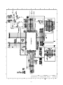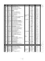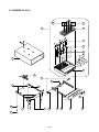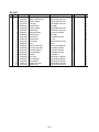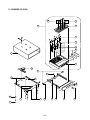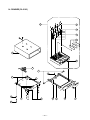
1
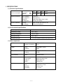
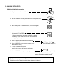
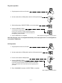
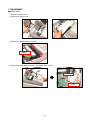
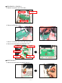
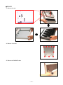
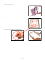
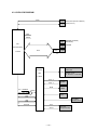
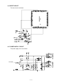
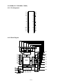
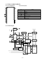
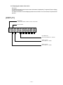
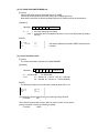
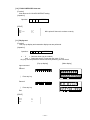
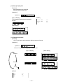
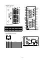
SERVICE MANUAL
(without price)
ELECTRONIC CASH REGISTER
TK-3200
(EX-585)
SEP. 2005
Printer Model: M-U420-061
INDEX
CONTENTS
TK-3200
PAGE
1. SPECIFICATIONS........................................................................................ 1
2. MACHINE INITIALIZATION ......................................................................... 3
3. DISASSEMBLY ............................................................................................ 6
4. CIRCUIT EXPLANATION .......................................................................... 14
5. DIAGNOSTIC OPERATION ....................................................................... 26
6. ERROR CODE LIST................................................................................... 46
7. IC DATA ..................................................................................................... 50
8. PCB LAYOUT ............................................................................................ 54
9. CIRCUIT DIAGRAMS ................................................................................. 57
10. PARTS LIST ............................................................................................... 73
To prevent malfunctions caused by the weak batteries, charge the memory
protection batteries for over 12-hours before installation or after a long-time
vacation (over 30 days).
• Before installation, initialize the terminal and leave it turn on over 12-hours.
• After a long-time vacation, initialize the terminal and restore the program data if
the terminal is in malfunction, and leave it turn on over 12-hours.
• Over 48-hours charging makes the batteries fully charged.
1. SPECIFICATIONS
1-1. Electrical specifications
120 V
Max. 0.6 A
Max. 0.01 A
220 V
0.3 A
0.06 A
230 V
0.3 A
0.06 A
240 V
0.3 A
0.06 A
•Power consumption
In operation
stand-by
•Memory protection
Back-up battery
Back-up period
Battery life
Recharge time
VL3032/1F2
90 days (25 °C)
Replace the battery every 5 years.
48 hours (full charge)
•Clock & Calendar
Accuracy
Auto calendar
Within ± 30 sec. per month (25 °C)
Effective until 2099 A.D.
1-2. Environmental specifications
• Operating temperature
0 °C ~ 40 °C
• Operating humidity
10 % ~ 95 %
• Storage temperature
-25 °C ~ 65 °C
• Storage humidity
10 % ~ 95 %
• Vibration strength
1.5 G (The machine must be in the carton box)
1-3. Main components
• CPU
Name
Number of control bit
uPD784215AGC
16 bit
• RAM
Name
Capacity
CY62148BLL-70SXC
4 Mbit
• Flash ROM
Name
Capacity
MBM29F160BE90TN
16 Mbit
• I/O controller
Name
uPD784215AGC
• Printer
Name
Print method
Paper cut
MCBF
M-U420-061
Impact dot matrix printer
Manual-paper cut
4 Million lines
• Roll paper
Type
Size
Roll diam
Thickness
Fine-quality paper
Width 44.5 ± 0.5 mm
83 mm or less
75 ± 15 µm
—1—
1-4. Drawer List
Type
Drawer Name
Specification
M
DL-2101
D-24H2C-B84M-9*
M
DL-2102
D-24H2C-B84SM-9*
M
DL-2103
D-24H2C-A84SM-9*
B
D
BU
Note: Country code
B: Europe
D: England
BU: Other countries
1-5. Option List
Device Name
Model
• Multi drawer kit
MDL-10
• PC cable
PRL-CB-2
Note
Applicable
• Waterproof cover
WT-78
For stroke key
• Sheet cover
WT-79
For touch key
• Slip printer
SP-1300
• Slip printer cable
PRT-CB-8C
• Remote printer
UP-360
• Printer cable
PRT-CB-8A
Length 3m
• Printer cable
PRT-CB-8B
Length 5m
• Slip printer/ AC adaptor
31AD-U or E
U: 120V/ E: 230V
• Handy scnner
HHS-15
Com2 port only
• Handy scnner
HS1250
Com2 port only
Local purchase
• Handy scanner
Quic Scan 6000
Com2 port only
Local purchase
• CF Memory Card
SDCFB-xx-505
56k V92 External
Local purchase
Length 1.5m
Local purchase
Local purchase
• Modem
Faxmodem
• Modem
56k Faxmodem
• Conversion Kit
CVK-S3-M/CVK-L3-M
• In line Kit
I/O-PB-18
• Roll paper
P-4575
For ArcNet board
CAUTION
RISK OF EXPLOSION IF BATTERY IS REPLACED
BY AN INCORRECT TYPE.
DISPOSE OF USED BATTERIES ACCORDING
TO THE INSTRUCTIONS
—2—
Local purchase
2. MACHINE INTIALIZATIO
Machine initialization procedure
1. Plug the power cord into an AC outlet.
REG2
REG1
2. Set the mode switch to PGM position and turn off the power switch.
OFF
X1
Z1
X2/Z2
RF
PGM
3. While holding down <JOURNAL FEED>, turn on the register.
4. Release <JOURNAL FEED>.
You should see “0000000000” on the display.
If 10 zeros are not shown or another character are shown,
immediately set the mode switch to OFF and restart from
the beginning of this procedure.
RECEIPT
FEED
RECEIPT
FEED
JOURNAL
FEED
5. Enter 11-digit program code from the worksheet.
6. Press <SUBTOTAL> to register the program code.
(Wait until beep twice.)
D11D10D9D8 ~ D3D2D1
refer to Worksheet (Initialize 1)
7. In case of installing inline system,
enter 3-digit program code from the worksheet.
8. Press <SUBTOTAL> to register the program code.
D3D2D1
refer to Worksheet (Initialize 2)
After completion of initialization and program
loading, initialization receipt is issued.
Please turn on and initialize the register in order, if your registers are connected with inline.
The ID number of registers are defined automatically.
(Do NOT turn off the register(s) until all register has been initialized.)
—3—
Worksheet (Initialize 1)
Description
Choice
Print password of PGM mode, when flag clear operation is performed.
Password in PGM3 ~ 7 mode
Messages and descriptors are written in
English = 0, French = 1, Spanish = 2, German = 4
Model for
U.S. or Canada (Date order: month/day/year)
= 4,
Other area (0.00, Date order: day/month/year)
= 1,
Other area (0, Date order: day/month/year)
=3
Fixed value: 08
Initialization pattern:
1 For scanning/ 2 For check tracking
Use Euro only.
Yes = 0
No = 4
Significant
numbers
Significant
number
Significant
number
Program code
D11
D10 D9 D8 D7
D6
D5
0 8
D4 D3
1 =0
2 =2
D2
No = 0
Yes = 1
D1
Choice
Program code
Worksheet (Initialize 2)
Description
156 kbps = 1
312 kbps = 0
Significant
numbers
Inline baud rate
Inline physical I.D. (01 ~ 32)
D3
D2 D1
Note:
Please check the receipt after initialization operation (machine initialization, flag clear operation and init2) that
the machine number is printed properly.
If error codes are printed on it, check the hardware and retry the operation.
P01
C01
03-04-2004
MC#01
11:58
000001
INIT
(C) 2005 by CASIO
COMPUTER CO.,LTD.
All rights reserved.
Mode symbol/date/time
Clerk descriptor/Mc-No./consecutive No.
INIT symbol
Copyright
TK-3200 STD
Model name
VER.
LABEL
ROM version
ROM label
:nnnn
:nnnnnn
VER.
:nnnn
LABEL :nnnnnn
INIT.
:nnnnnnnnnnnnnn
0004-98
:
00
2000
ROM version
ROM label
Initialization code
I/O parameter table record No./error code
—4—
Flag clear operation
1. Plug the power cord into an AC outlet.
2. Set the mode switch to PGM position and turn off the power switch.
REG2
REG1
X1
Z1
OFF
X2/Z2
RF
PGM
3. While holding down <RECEIPT FEED>, turn on the register.
4. Release <RECEIPT FEED>.
You should see “FFFFFFFFFF” on the display.
TJOURNAL
FEED
RECEIPT
FEED
If 10 Fs are not shown or another character are shown,
immediately set the mode switch to OFF and restart from
the beginning of this procedure.
JOURNAL
FEED
After completion of flag clear, receipt is issued.
5. Press <SUBTOTAL> to complete.
Note: After flag clear, clerk 1 is assigned automatically. So do not program clerk 1 as not assignable or
not operable in PGM mode.
Init 2 operation
1. Plug the power cord into an AC outlet.
TJOURNAL
FEED
2. Set the mode switch to PGM position and turn off the power switch.
REG2
REG1
3. Turn the mode switch to PGM position.
X1
OFF
4. Release <RECEIPT FEED>.
You should see “FFFFFFFFFF” on the display.
Z1
X2/Z2
RF
PGM
If 10 Fs are not shown or another character are shown, immediately
set the mode switch to OFF and restart from the beginning of this
procedure.
RECEIPT
FEED
JOURNAL
FEED
5. Enter “8888888888” and press <CHECK TEND> to complete.
After completion, receipt is issued.
—5—
3. DISASSEMBLY
■ UPPER CASE
1. Remove the Printer cover.
2. Remove the Ribbon cover.
2
1
3. Remove the Ribbon and then 2 screws.
Ribbon
4. Lift the upper case and then remove 2 connectors (CN11, CN12).
1
CN12
2
CN11
—6—
■ PCB (E585-E2-1, E585-E6-1)
5. Remove 3 connectors. (CN1, CN2, CN3)
CN2
CN1
CN3
6. Remove the E585-E2-1 PCB.
7. Remove 5 connectors. (CN1, CN2, CN3, CN4, CN5)
8. Remove the screw and then the E585-E6-1 PCB.
CN1
CN5
CN3
CN4
CN2
■ MODE SW ASS’Y
9. Remove the screw and then the MODE SW ASS’Y.
—7—
■ PCB (E585-E6-2)
10. Remove 2 screws and then the E585-E6-2 PCB.
NOTE: Be fully careful not to miss the Defect button when removing the E585-E6-2 PCB.
■ KEY BOARD ASS’Y
11. Remove 7 screws and then the KEY BOARD ASS’Y
SHEET/COMMON
SPACER
12. Remove 18 screws and then disassemble the keyboard ass’y.
FPC
CHASSIS
—8—
■ MAIN PCB (E585-1)
13. Remove the connector (CN10).
14. Remove the backup battery.
15. Remove 4 connectors (CN3, CN5, CN8, CN13).
16. Remove 4 screws.
CN5
CN8
CN13
CN3
17. Remove the MAIN PCB (E585-1).
—9—
■ PRINTER UNIT
18. Loosen 4 screws.
19. Lift the printer unit and then remove the screw.
— 10 —
■ POWER SUPPLY
20. Remove 2 screws and then Rear connector cover.
21. Remove 3 screws and then Power supply cover.
22. Remove 4 screws and then Power supply cover.
— 11 —
■ DRAWER
23. Remove the case.
24. Remove 10 screws.
25. Remove the DARWER cable.
— 12 —
26. Remove the Bottom plate.
27. Loosen 4 screws.
28. Remove the screw and then fix the drawer case.
— 13 —
4. CIRCUIT EXPLANATION
4-1. HARDWARE DIAGRAM
Main Display
Popup
display
Journal printer
Sheet ke
y hold
er
Keyboard
Receipt printer
Power
supply
CPU
Flash
Memory
RAM
512kB
2MB
Popup
disp.
i/f
Drawer
Drawer
1 i/f
2 i/f
RS232C
COM1
RS232C
COM2
CF card
Drawer
Scanner
HHS-15
Slip
printer
SP-1300
Power
supply
31AD-U/E
Other
Terminal
Other
Terminal
Other
Terminal
Note: Shadowed device and dot line indicate option devices.
— 14 —
PRT-CB-8A/-8B
either
or
MODEM
or
PC
PRT-CB-8C
PRL-CB-2
CASIO
original cable
Inline-2 Inline-1
CAT5 UTP cable
Drawer
Multi drawer kit MDL-10
Inline(I/O-PB18)
External
printer
UP-360
Power
supply
4-2. BLOCK DIAGRAM
ModeSW
E475-E3
E585-E2-2
* 7seg × 8 + TRN × 2
Dot PRN UNIT
M-U420-61
Switch × 8
12pin
10pin
E585-E2-1
Manual Cutter
E585-E6-1
* 7seg × 10 + 14seg × 10 + TRN × 8
B20B-PHDSS(20pin)
Power × 4
LED_Latch × 7
LED_DATA × 8
LED_CE × 1
Reset_SW
CN13(29pin)
Battery
B20B-PHDSS
CN12(20pin)
CN10(2pin)
8pin
Common
(5pin)
Segment
(3pin)
9pin
30pin
16pin+11pin
4pin
B30B-PHDSS
GND × 1
SW_in × 1
Mode × 1
Key × 27
E545-E4
Sheet SW
Key (FPC)
E585-E6-2
B30B-PHDSS
CN11(30pin)
CN9(2pin)
SRAM
512KB
Flash ROM
2MB
ID9P33E4GX28
CN4(9pin) COM1
CPU
78K4
(12.5MHz)
I/O
78K4
(12.5MHz)
B8B-PH-SM3-TB
CN3(9pin)
8pin
COM2
With 5V
5pin
CN8
B3B-PH-SM3-TB
Standard
Option
CN5(3pin) CN6(3pin)
POWER
SUPPLY
UNIT
SW
CN1(28pin)
SW
CF card I/F
(62451-022L)
E585-1 PCB
E445-S1
DRAWER
POWER CORD
— 15 —
E466-ARC
2pin
E468-ARC
4-3. LSI BLOCK DIAGRAM
Serial
RS232C
COM1(Correspondence Modem )
RS232C
COM2(w th 5V)
SRAM
4 Mbit
PRGRAM (SHADOW)
Data BackUp
FROM
16 Mbit
PRGRAM
PWD
RESET
CPU
uPD784215AGC
buffer
BUS
12.5MHz
3.3V
CF CAR
5V
I/O
Controller
REAR DISPLAY
7SEG LED
LATCH
78K4
MAIN DI PLAY
14 EG LED + 7 EG LED
12.5MHz
Drive × 2
status × 2
BUZZ
from HardReset
DRAWER
×2
BUZZER
RESET
from CPU PORT
Switch
RTS
CTS
KEY SHEET
(STROKE+FLAT)
DTR
DSR
RxD/TxD
Drive
Sensor
— 16 —
Dot Printer
(Receipt+Journal)
4-4. RESET CIRCUIT
The reset circuit is as follows.
4-5. POWER SUPPLY CIRCUIT
The power supply circuit is as follows.
IC32 32pin
— 17 —
4-6. DRAWER I/F CIRCUIT
The drawer open circuit is as follows.
— 18 —
4-7. PRINTER CONTROL CIRCUIT
The printer control circuit is as follows.
— 19 —
4-8. CPU (IC32: uPD784215AGC279-8EUA) / I/O CONTROLLER (IC44: uPD784215AGC280EUA)
P63/A19
P64/RD
P66/WAIT
P65/WR
P67/ASTB
P101/TI6/TO6
P100/TI5/TO5
VDD
P103/TI8/TO8
P102/TI7/TO7
P30/TO0
P33/TI1
P32/TO2
P31/TO1
P35/TI00
P34/TI2
P95
P94
P93
P92
P91
P90
TEST/VPP
P37/EXA
P36/TI01
4-8-1. Pin Assignment
100 99 98 97 96 95 94 93 92 91 90 89 88 87 86 85 84 83 82 81 80 79 78 77 76
75
P62/A18
74
73
72
P61/A17
P120/RTP0
P121/RTP1
P122/RTP2
1
2
3
P123/RTP3
4
P124/RTP4
P125/RTP5
P126/RTP6
P127/RTP7
VDD
5
6
71
P60/A16
VSS
P57/A15
70
P56/A14
7
8
69
68
67
P55/A13
P54/A12
P53/A11
P52/A10
P51/A9
20
21
22
23
24
55
54
— 20 —
P81/A1
P82/A2
P25/SI0/SDA0
P26/SO0
P27/SCK0/SCL0
P80/A0
P20/RxD1/SI1
P21/TxD1/SO1
P22/ASCK1/SCK1
P23/PCL
P24/BUZ
P71/TxD2/SO2
P72/ASCK2/SCK2
P131/ANO1
AVREF1
P70/RxD2/SI2
25
26 27 28 29 30 31 32 33 34 35 36 37 38 39 40 41 42 43 44 45 46 47 48 49 50
AVSS
P10/ANI0
58
57
56
P130/ANO0
AVDD
AVREF0
60
59
17
18
19
P17/ANI7
P05/INTP5
P06/INTP6
14
15
16
P14/ANI4
P15/ANI5
P16/ANI6
P02/INTP2/NMI
P03/INTP3
P04/INTP4
66
65
64
63
62
61
P13/ANI3
P00/INTP0
P01/INTP1
9
10
11
12
13
P11/ANI1
P12/ANI2
X2
X1
VSS
XT2
XT1
RESET
53
52
51
P50/A8
P47/AD7
P46/AD6
P45/AD5
P44/AD4
P43/AD3
P42/AD2
P41/AD1
P40/AD0
P87/A7
P86/A6
P85/A5
P84/A4
P83/A3
4-8-2. Block Diagram
INTP2/NMI
INTP0, INTP1,
INTP3-INTP6
PROGRAMMABLE
INTERRUPT
CONTROLLER
UART/IOE1
BAUD-RATE
GENERATOR
TI00
TI01
TO0
TIMER/COUNTER
(16 BITS)
UART/IOE2
BAUD-RATE
GENERATOR
TI1
TO1
TIMER/COUNTER1
(8 BITS)
CLOCKED
SERIAL
INTERFACE
TI2
TO2
TIMER/COUNTER2
(8 BITS)
TI5/TO5
TIMER/COUNTER5
(8 BITS)
TI6/TO6
TIMER/COUNTER6
(8 BITS)
TI7/TO7
RxD1/SI1
TxD1/SO1
ASCK1/SCK1
RxD2/SI2
TxD2/SO2
ASCK2/SCK2
SI0
SO0
SCK0
AD0-AD7
A0-A7
A8-A15
TI8/TO8
BUS I/F
A16-A19
RD
WR
WAIT
ASTB
TIMER/COUNTER7
(8 BITS)
PORT0
P00-P06
PORT1
P10-P17
TIMER/COUNTER8
(8 BITS)
PORT2
P20-P27
PORT3
P30-P37
PORT4
P40-P47
PORT5
P50-P57
PORT6
P60-P67
PORT7
P70-P72
PORT8
P80-P87
PORT9
P90-P95
PORT10
P100-P103
PORT12
P120-P127
PORT13
P130,P131
WATCH TIMER
78K/IV
CPU CORE
ROM
RAM
WATCHDOG TIMER
RTP0-RTP7
NMI/INTP2
REAL-TIME
OUTPUT PORT
ANO0
ANO1
AVREF1
AVSS
D/A
CONVERTER
ANI0-ANI7
AVREF0
AVDD
AVSS
P03
A/D
CONVERTER
PCL
BUZ
RESET
X1
SYSTEM CONTROL
CLOCK OUTPUT
CONTROL
X2
XT1
XT2
BUZZER OUTPUT
VDD
VSS
— 21 —
4-8-3. Pin Function
PIN NO.
1
2
3
4
5
6
7
8
9
10
11
12
13
14
15
16
17
18
19
20
21
22
23
24
25
26
27
28
29
30
31
32
33
34
35
36
37
38
39
40
41
42
43
44
45
46
47
48
49
50
PIN NAME
P120/RTP0
P121/RTP1
P122/RTP2
P123/RTP3
P124/RTP4
P125/RTP5
P126/RTP6
P127/RTP7
VDD
X2
X1
VSS
XT2
XT1
RESET
P00/INTP0
P01/INTP1
P02/INTP2/NMI
P03/INTP3
P04/INTP4
P05/INTP5
P06/INTP6
AVDD
AVREF0
P10/ANI0
P11/ANI1
P12/ANI2
P13/ANI3
P14/ANI4
P15/ANI5
P16/ANI6
P17/ANI7
AVSS
P130/ANO0
P131/ANO1
AVREF1
P70/RxD2/SI2
P71/TxD2/SO2
P72/ASCK2/SCK2
P20/RxD1/SI1
P21/TxD1/SO1
P22/ASCK1/SCK1
P23/PCL
P24/BUZ
P25/SI0/SDA0
P26/SO0
P27/SCK0/SCL0
P80/A0
P81/A1
P82/A2
I/O
IO
I
I
I
IO
DESCRIPTION
8 bit input/output PORT
Power Supply
Main system Clock
GND
Sub system Clock
Reset
7 bit input/output PORT
-
A/D CONVERTER POWER SUPPLY
Application of Standard Voltage for A/D CONVERTER
I
8 bit input PORT
A/D CONVERTER & D/A CONVERTER GND
IO
2 bit input/output PORT
Application of Standard Voltage for D/A CONVERTER
IO
3 bit input/output PORT
IO
8 bit input/output PORT
IO
8 bit input/output PORT
— 22 —
PIN NO.
51
52
53
54
55
56
57
58
59
60
61
62
63
64
65
66
67
68
69
70
71
72
73
74
75
76
77
78
79
80
81
82
83
84
85
86
87
88
89
90
91
92
93
94
95
96
97
98
99
100
PIN NAME
P83/A3
P84/A4
P85/A5
P86/A6
P87/A7
P40/AD0
P41/AD1
P42/AD2
P43/AD3
P44/AD4
P45/AD5
P46/AD6
P47/AD7
P50/A8
P51/A9
P52/A10
P53/A11
P54/A12
P55/A13
P56/A14
P57/A15
VSS
P60/A16
P61/A17
P62/A18
P63/A19
P64/RD
P65/WR
P66/WAIT
P67/ASTB
VDD
P100/TI5/TO5
P101/TI6/TO6
P102/TI7/TO7
P103/TI8/TO8
P30/TO0
P31/TO1
P32/TO2
P33/TI1
P34/TI2
P35/TI00
P36/TI01
P37/EXA
TEST/VPP
P90
P91
P92
P93
P94
P95
I/O
DESCRIPTION
IO
8 bit input/output PORT
IO
8 bit input/output PORT
IO
8 bit input/output PORT
-
IO
-
GND
8 bit input/output PORT
Power Supply
IO
4 bit input/output PORT
IO
8 bit input/output PORT
-
IO
TEST pin
6 bit input/output PORT
— 23 —
4-9. SRAM (IC6: CY62148BLL-70SXC)
4-9-1. Pin Assignment
A17
A16
A14
A12
A7
A6
A5
A4
A3
A2
A1
A0
I/O0
I/O1
I/O2
VSS
32
31
30
29
28
27
26
25
24
23
22
21
20
19
18
17
1
2
3
4
5
6
7
8
9
10
11
12
13
14
15
16
VCC
A15
A18
WE
A13
A8
A9
A11
OE
A10
CE
I/O7
I/O6
I/O5
I/O4
I/O3
4-9-2. Block Diagram
I/O 1
Data in Drivers
CE
I/O 2
I/O 3
SENSE AMPS
ROW DECODER
A0
A1
A2
A3
A4
A5
A6
A7
A8
A9
512K x 8
ARRAY
I/O 5
I/O 6
COLUMN
DECODER
POWER
DOWN
I/O 7
I/O 8
A10
A11
A12
A13
A14
A15
A16
A17
A18
WE
OE
I/O 4
— 24 —
4-10. FROM (IC4: MBM29F160BE90TN)
4-10-2. Pin Function
4-10-1. Pin Assignment
A15
1
48
A16
A14
2
47
BYTE
A13
3
46
VSS
A12
4
45
DQ15/A-1
A11
5
44
DQ7
A10
6
43
DQ14
A9
7
42
DQ6
A8
8
41
DQ13
Pin
Function
A-1, A0 to A19
DQ0 to DQ15
CE
Address Inputs
Data Inputs/Outputs
Chip Enable
A19
9
40
DQ5
OE
Output Enable
N.C.
10
39
DQ12
WE
Write Enable
WE
11
38
DQ4
RESET
12
37
VCC
RY/BY
Ready/Busy Output
N.C.
13
36
DQ11
RESET
Hardware Reset Pin/Temporary Sector Unprotection
WP
14
35
DQ3
BYTE
RY/BY
15
34
DQ10
N.C.
No Internal Connection
A18
16
33
DQ2
VSS
Device Ground
A17
17
32
DQ9
A7
18
31
DQ1
VCC
Device Power Supply
A6
19
30
DQ8
A5
20
29
DQ0
A4
21
28
OE
A3
22
27
VSS
A2
23
26
CE
A1
24
25
A0
Selects 8-bit or 16-bit mode
4-10-3. Block Diagram
RY/BY
Buffer
RY/BY
DQ0 to DQ15
VCC
VSS
Erase Voltage
Generator
WE
BYTE
RESET
Input/Output
Buffers
State
Control
Command
Register
Program Voltage
Generator
Chip Enable
Output Enable
Logic
CE
STB
Data Latch
OE
STB
Low VCC Detector
Timer for
Program/Erase
A0 to A18
A-1
— 25 —
Y-Decoder
Address
X-Decoder
Latch
Y-Gating
Cell Matrix
5. DIAGNOSTIC OPERATION
5-1. To start the diagnostic program
To enter the diagnostic program, press ”99990000<ST>” right after reset-and-start, IPL boot or INT
operation. In QA DIAG (factory module also) module, the mode transfers to the diagnostic mode after
INT operation.
* Reset-and-start
1 Press the reset switch while pressing JFEED button.
2 When “INT” appears in the first line of the LCD dot line, press<SUBTOTAL>.
3 When “INT” appears in the second line of the LCD dot line, press”99990000<SUBTOTAL>”.
4 Enter the diagnostic mode.
* INT operation
1 While holding down the JFEED button, align the mode key with “PGM” using the OW key.
2 When “INT” appears in the second line of the LCD dot line, press “99990000<SUBTOTAL>”.
3 Enter the diagnostic mode.
* In the case if “MASK DIAG” is displayed and the counter is activated
A false operation has led to the MASK diagnostic mode. Perform IPL operation again.
5-2. Displaying and printing the version
The version of DIAG and MADK ROM/IOC are printed immediately after entering the DIAG mode.
However, DIAG/IOC version printing function is available only in QA DIA module.
• All test results are printed by the built-in printer receipt.
I o
Ma
D i
Ma
c
Ve
s k Ve
ag Ve
y 17
r
r
r
20
: 4 2 1 6 A AOCA A
: 4 2 0 7 AAOAAA
:
05
10 : 08
IOC
MASK ROM
DIAG
5-3. Notes for the DIAG
• All test result are printed by the built-in receipt printer.
• Make sure to test HHS-15 by connecting to COM2.
• To perform the continuous check, follow the direction for each test, and input numbers except 0. Input
numbers 1-9 as the command how many times to perform the test for the operation in each page to
perform continuous check. Note that you can only choose one time check or continuous check.
• When turn off by rotating the key, the display is unlit, and DAIG command is not accepted.
[Others]
• ESC value is printed as follows if the test ended by force. Press the “C” key or turn off the power to end
the test while performing continuous check. The result of ending by force is not printed in each test.
| ESC
|
— 26 —
5-4. Displaying the status of the device
[Function]
The status of the device which has the status information is displayed by 7 segments (Pop-up display)
as well as lit transaction.
The status information and the displayed position are as follows. As for tact switch, the pressed LED
will be lit.
[DISPLAY]
Mode display
1:PGM, 2:RF, 3:REG1, 4:REG2, 5:X 6:Z, 7:XZ2, 8:OFF
Menu sheet NO.
CF CARD sensor
Off : Not yet inserted On : Inserted
Drawer 1 sensor
Off : CLOSE On : OPEN
Drawer 2 sensor
Off : CLOSE On : OPEN
— 27 —
5-5. Check item
The following test can be checked in the diagnostic test.
No
Device to be checked
1 Batch test 1
Operation
1
2
3
4
5
6
7
8
9
10
12
13
15
16
17
18
19
20
21
22
23
24
25
2
n011
n111
0n013
0n113
0n213
0n313
x1x20016
212
n021
221
n321
421
521
cn03d
26
27
28
29
30
31
Batch test 2
RAM WRITE/READ test
RAM READ ONLY test
CF-CARD WRITE/READ test
CF-CARD READ ONLY test
CF-CARD CLEAR test
CF-CARD CLEAR WRITE/READ test
Locale information write
FLASH USER AREA clear test
Display test
7 Segment display test
LCD test
LCD CONTRAST ADJUSTMENT
Display test (repeat)
Internal printer print test
Internal printer graphic print test
Internal printer dot rate test
Internal printer print value test
Internal printer print density test
COM (RS232C) test
COM (RS232C) batch test
Time setting
Time display
Drawer open test
Buzzer test
Consumption current
KEY dipsplay
OBR test
Displaying the battery voltage
Note
Test Device : RAM, Printer, Date,
Time, Buzzer, Drawer
Test Device : Display, Back light
Page
32
x1x2x3x4x5x60a70
32
33
34
34
35
35
36
36
37
38
39
40
41
42
43
44
45
46
46
47
48
49
70
xn091
n092
193
94
95
96
50
50
51
52
53
54
P1P1P1P2P2P2n13d
pn33d
435
x0235
xn04d
40
— 28 —
5-6. Operation of each test
[ 1 ] Batch test 1
[Function]
RAM test, test print, time setting, buzzer test and drawer open test are performed continuously.
[Operation]
Operation :
[Pop-up display]
1
n
SUBTOTAL
The following tests are performed
automatically.
(1) RAM test: WRITE/READ area test.
(2) Test print
(3) Time setting: Set the following data.
Arranged data: 2005 December
31,23:59’30
(4) Buzzer: Ring once the one shot buzzer.
No print or display in this test.
(5) Drawer open: Drawer 1 opens only.
(6) Receipt issuance
n=0 1 2 3 2 3
[Main display]
D I AG
1
00n
n=0 1 2 3 2 3
[Print]
* Normal print
BA TCH
1
R A M WR
OK
BBBBBBBBBBBBBBBBBBBBBBBB
DATE
05 / 12 / 31
T I ME
23 : 59 - 30
D RW 1
OK
END
1
Print Test
* See “RAM test” if “ERROR” appears while
performing the RAM test.
[ 2 ] Batch test 2
[Function]
Display test is performed continuously.
[Pop-up display]
[Operation]
Operation :
2
Refer to each item.
SUBTOTAL
[Main display]
The following tests are performed
automatically.
(1) Display test: Refer to “[12] Display test.”
Press any key to go to the next test.
(2) Main test: Refer to “[15] LCD test.”
(3) Pop-up display test: Perform Pop-up
display test. See “[14]” for more
information.
(4) Backlight test: Refer to “[13]” for more
information.
Perform the backlight test.
The backlight color changes if any key is
depressed.
Refer to the “Backlight test” for details.
(5) Receipt issuance
— 29 —
Refer to each item.
[Print]
* Normal print
BA TCH
D I SP
D I S P MA I N
D I SP 7 SEG
B ACK L I GH T
END
2
OK
OK
OK
OK
2
[ 3 ] RAM WRITE/READ test
[Function]
This test will check the WRITE/READ test for RAM.
A counter is displayed for the RAM test.
Write and read test is performed in the sequence as following. Write common (system area) and
read write common( other than the system area) and read write each bank read each bank.
Also, the test is not performed for the range to (-4000H) by the handler.
[Operation]
Operation :
n
0
1
1
SUBTOTAL
n : 0
= One time check (can be omitted)
not 0 = Continuous check (To stop the test, press “C” key)
[Pop-up display]
A counter is displayed for Pop-up display.
n
n=0 1 2 3 2 3
[Main display]
D I AG
0011
00n
n=0 1 2 3 2 3
[Print]
The result of all area for RAM test is printed as follows.
RAM
R A M WR
END
11
OK
11
* The result is printed as follows if the test ended with an error.
If an error occurs while checking the BANKO address 0x60400 for normal RAM
R A M WR
NG
BANK 0 - 6 0 4 0 0
* The result is printed as follows if the test ended with an error.
Print
RAM WR NG-*****
RAM WR NG BANKO-*****
RAM WR NG BANK1-*****
NG
NG if the COMMON address for RAM is ******* to 1Kbyte.
NG if the BANKO address for RAM is ********to 1Kbyte.
NG if the BANK1 address for AM is *******to 1Kbyte.
— 30 —
[ 4 ] RAM READ ONLY test
[Function]
RAM READ ONLY test is performed.
Perform the WRITE test (n011) right before start of this test.
System area test for COMMON is not performed.
[Operation]
Operation :
n
1
1
1
SUBTOTAL
n : 0
= One time check (can be omitted)
not 0 = Continuous check ( Press the “C” key or turn off the power by rotating the key to
end the test.)
[Pop-up display]
A counter is displayed for Pop-up display.
[Main display]
D I AG
0111
n
00n
n=0 1 2 3
n=0 1 2 3
[Print]
The result for all area test for RAM is printed as follows.
RAM
RAM RD
END
111
OK
111
Address of an error is printed if the test ended with an error.
* Refer to RAM WRITE/READ test when NG is printed.
[ 5 ] CF-CARD WRITE/READ test
[Function]
This test will check the write/read test (connection test) for CF-CARD.
Perform the CF-CARD clear test, before start of this test.
Note that this test does not ensure the data inside the CF-CARD as well as its performance.
[Operation]
Operation :
0
n
0
1
3
SUBTOTAL
n : 0
= One time check( can be omitted)
not 0 = Continuous check (To stop the test, press “C” key or turn off the power by rotating
the key.)
[PRINT]
CF - CARD
CF
WR
END
13
OK
13
NG and the address are printed if WRITE cannot be done
normally.
— 31 —
[ 6 ] CF-CARD READ ONLY test
[Function]
This test will check the read only test for CF-CARD.
Perform the CF-CARD write test, before start of this test.
Note that this test does not ensure the data inside the CF-CARD as well as its performance.
[Operation]
Operation :
0
n
1
1
3
SUBTOTAL
n : 0
= One time check(can be omitted)
not 0 = Continuous check( To stop the test, press ”C” key or turn off the power by rotating
the key.)
[PRINT]
CF - CARD
CF
RD
END
113
OK
113
NG and the address are printed if READ cannot be done
normally.
[ 7 ] CF-CARD CLEAR test
[Function]
This test will check the clear test for CF-CARD.
Note that this test does not ensure the data inside the CF-CARD as well as its performance.
[Operation]
Operation :
0
n
2
1
3
SUBTOTAL
n : 0
= One time check (can be omitted)
not 0 = Continuous check (To stop the test, press “C” key or turn off the power by rotating
the key.)
[PRINT]
CF - CARD
CF
CLR
END
213
OK
213
NG and the address are printed if WRITE cannot be done
normally.
— 32 —
[ 8 ] CF-CARD CLEAR WRITE/READ test
[Function]
This test will check the clear write/read test for CF-CARD.
Perform the write/read test (connection check) after clearing all memory.
Note that this test does not ensure the data inside the CF-CARD as well as its performance.
[Operation]
Operation :
0
n
3
1
3
SUBTOTAL
n : 0
= One time check(can be omitted)
not 0 = Continuous check (To stop the test, press “C” key or turn off the power by rotating
the key.)
[PRINT]
CF - CARD
CF
C L R &WR
END
313
OK
313
NG and the address are printed if WRITE cannot be done
normally.
[ 9 ] Locale information write
[Function]
The Locale information is written into FLASH MEMORY.
[Operation]
Operation : x1 x2
0
0
1
6
SUBTOTAL
x1 : xcountry code,
x2: SUB CODE
x1 x2:
10 Europe, 20 US, 30 UK, 40 Germany,
50 Canada, 60 Direct, 61 Direct (Hebrew)
[PRINT]
The following receipt is not issued when commands other than x1, x2.
L OCA L E
L OCA L E
END
x1x2 0 0 1 6
OK
x1x2 0 0 1 6
The following is printed when an error occurs during writing LOCALE.
| LOCALE
NG
|
The LOCALE can be written 5 times. When no more LOCALE can be written
(writing more than 5 times), the following is printed.
| LOCALE
OVER
|
— 33 —
[ 10 ] FLASH USER AREA clear test
[Function]
Clear the area of LOCALE/CONTRAST setting.
[Operation]
Operation :
2
1
2
SUBTOTAL
[PRINT]
R OM
R OM C L R
END
212
OK
212
NG is printed if the test is not done correctly.
[ 11 ] Display test
[Function]
LCD, Pop-up display and transaction display tests are performed.
[Operation]
Operation :
n
0
2
1
SUBTOTAL
n : 0
= One time check (can be omitted)
not 0 = Continuous check (To stop the test, press “C” key)
* Any key must be pressed to end the test when performing one time check.
[Pop-up display]
Input command
Pattern 1
Press any key
Pattern 2
Press any key
End
[PRINT]
D I SP
D I SP
END
21
OK
21
— 34 —
[Main display]
[ 12 ] Pop-up display test
[Function]
Pop-up display test is performed.
Press any key to end the test.
[Operation]
Operation :
2
2
1
SUBTOTAL
[Pop-up display]
The following is displayed and cleared after
the test.
[PRINT]
D I SP
D I SP
END
7 SEG
7 SEG
221
OK
221
[Main display]
[ 13 ] Display test (repeat)
[Function]
LCD, Pop-up display and transaction display tests are performed.
[Operation]
Operation :
5
2
1
SUBTOTAL
* Press “C” key or turn off the power to stop the test.
[Pop-up display]
Pattern 1
Pattern 2
“C” key
End
[PRINT]
D I SP
D I SP
END
521
OK
521
— 35 —
[Main display]
[ 14 ] Internal printer print test
[Function]
This test will check the characters in the receipt/journal of the internal printer.
[Operation]
Operation :
c: 0
1
n: 0
not 0
d: 3
4
5
c
n
0
3
d
SUBTOTAL
=
=
=
=
prints character’ B’
prints all characters
One time check
Continuous check (To stop the test, press “C” key or turn off the power by rotating
the key.)
= prints only receipt
= prints only journal
= prints both receipt/journal (prints alternately)
[Print]
1. prints character’ B’
BBBBBBBBBBBBBBBBBBBBBBBB
2. prints all characters
The printing order is in the order of the character code. The characters from 0x20(SP) to 0xFA(•)
are printed.
A space is printed for a code without the printing character.
A character which cannot be printed is a character within the range of the code 0x00 to 0x1F and
0xFB to 0xFF.
— 36 —
[ 15 ] External printer print test
[Function]
This test will check the print test for the RS232C I/F printer.
Connect the printer to the COM which is to be tested.
[Operation]
Operation :
x1 x2 x3
n
0
3
d
SUBTOTAL
X1: Print test pattern
0 = A pattern, 1 = B pattern
X2: Port selection
1 = COM1, 2 = COM2
X3: Baud rate selection
1 = 4800 bps, 2 = 9600 bps, 3 = 19.2 kbps
n: 0 = One time check (can be omitted)
not 0 = Continuous check (To stop the test, press “C” key)
d: Printer type selection
1 = UP360, 2 = SP1300
Note that some printers cannot use certain baud rates. Refer to the list below.
When changing the baud rate, make sure to change the setting for the printer also.
19.2 Kbps 9600 bps 4800 bps
SLIP PRINTER (SP1300)
✕
Ο
Ο
RJ PRINTER (UP360)
Ο
Ο
Ο
[Print]
Printing pattern is the following 2types.
The number of lines : 40 lines for RJ and 35 lines for SLIP.
BBBBBBBBBBBBBBBBBBBBBBBBBBBBB
A pattern
B pattern
— 37 —
[ 16 ] COM (RS232C) test
[Function]
This is the RS232C test.
The loop back test for RS232C port is performed by making the connection shown in the figure.
Refer to [ 24 ] COM (RS232C) batch test the figure for RS232C port connection.
[Operation]
Operation :
x
n
0
4
d
SUBTOTAL
x :
Baud rate selection
0
= 2400 bps, 1=4800 bps, 2=9600 bps, 3=19.2 kbps
n : 0
= One time check (can be omitted)
not 0 = Continuous check (To stop the test, press “C” key)
d :
Port selection
1
= COM1
2
= COM2
[Print]
x=0, d=1
C OM 1
RTS1
DTR1
DTR1
DTR1
RTS1
DTR1
DTR1
DTR1
TxD
END
=
=
=
=
=
=
=
=
1
1
1
1
0
0
0
0
x=1~3, d=1
–
–
–
–
–
–
–
–
–
–
–
–
–
–
–
–
–
–
>
>
>
>
>
>
>
>
>
4
CTS1 =
DSR1 =
CD 1 =
CI 1=
CTS1 =
DSR1 =
CD 1 =
CI 1=
RxD
4
1
0
0
0
0
0
0
0
0
C OM 1
RTS1
DTR1
DTR1
DTR1
RTS1
DTR1
DTR1
DTR1
TxD
END
OK
OK
OK
OK
OK
OK
OK
OK
OK
1
x=0, d=2
C OM 2
RTS2
DTR2
RTS2
DTR2
TxD
END
=
=
=
=
1
1
0
0
=
=
=
=
=
=
=
=
1
1
1
1
0
0
0
0
–
–
–
–
–
–
–
–
–
–
–
–
–
–
–
–
–
–
>
>
>
>
>
>
>
>
>
x
CTS1 =
DSR1 =
CD 1 =
CI 1=
CTS1 =
DSR1 =
CD 1 =
CI 1=
RxD
x
n041
0
0
0
0
0
0
0
0
x
CTS2 =
DSR2 =
CTS2 =
DSR2 =
RxD
x
n042
0
0
0
0
OK
OK
OK
OK
OK
OK
OK
OK
OK
n041
x=1~3, d=2
–
–
–
–
–
–
–
–
–
–
>
>
>
>
>
4
CTS2 =
DSR2 =
CTS2 =
DSR2 =
RxD
4
2
0
0
0
0
C OM 2
RTS2
DTR2
RTS2
DTR2
TxD
END
OK
OK
OK
OK
OK
2
— 38 —
=
=
=
=
1
1
0
0
–
–
–
–
–
–
–
–
–
–
>
>
>
>
>
n042
OK
OK
OK
OK
OK
[ 17 ] COM (RS232C) batch test
[Function]
This is the RS232C port batch test.
The loop back test for RS232C port is performed by making the connection shown in the figure.
When performing this test, fix loop back connectors to all COM ports.
[Operation]
Operation :
4
0
SUBTOTAL
Baud rate: COM1: 19.2kbps, COM 2 : 9600 bps
Check time: one time (stable)
[Print]
C OM B A T C H
RTS1 = 1 – – >
DTR1 = 1 – – >
DTR1 = 1 – – >
DTR1 = 1 – – >
RTS1 = 0 – – >
DTR1 = 0 – – >
DTR1 = 0 – – >
DTR1 = 0 – – >
TxD
––>
RTS2 = 1 – – >
DTR2 = 1 – – >
RTS2 = 0 – – >
DTR2 = 0 – – >
TxD
––>
END
COM1
4
CTS1 =
DSR1 =
CD 1 =
CI 1=
CTS1 =
DSR1 =
CD 1 =
CI 1=
RxD
CTS2 =
DSR2 =
CTS2 =
DSR2 =
RxD
4
0
0
0
0
0
0
0
0
0
0
0
0
0
OK
OK
OK
OK
OK
OK
OK
OK
OK
OK
OK
OK
OK
OK
COM 1 test result
COM 2 test result
0
Figure : RS232C port connection
COM2
TxD
TxD
RxD
RxD
CTS
CTS
RTS
RTS
DTR
DTR
DSR
DSR
CD
CI
outputs "1" "0" from the output terminal and checks the input terminal.
— 39 —
[ 18 ] ARCNET test
[Function]
This test will check the counter-communication of ARCNET.
Always make the receive ECR in the wait mode first and then send data from the send ECR.
Continue the test while the communication is done normally.
The counter of the number of receive/send packets to LCD is displayed after the communication
normally starts. It is continuously displayed while the communication is done normally.
* send/receive data
SID DID LEN
DATA 00h~FFh, 00h~FBh
508 byte
LRC
1. Normal mode
When the receive ECR (a=2 below) receives the data normally, the test checks the received data,
reverse the received data (FBh – 01h, 00h, FFh – 00h), and sends back the data to the send ECR
(a= 1). The send ECR checks the reversed data. (The same repeats hereinafter)
* Retry
Receive ECR: Ignores the error until the number of error reaches consecutivel r times. Returns to
the wait mode afterwards.
Send ECR: Sends data one second after the receive ECR does not respond, and retries until r times.
Sends an error and ends afterwards.
2. Simultaneous mode
Checks only the received data when the receive ECR (a=4) receives the data normally.
The send ECR (a=3) waits for one second and start sending data again. (The same repeats
hereinafter)
[Operation]
* Make sure to check the ID upon setting the ID. When changing the ID, turn the power on again.
r
l
l
m
m
x
0
a
5
1
SUBTOTAL
r: the number of retries (1 – 9 times)
Then number of retries will be 5 when 0 or no input.
Note that the retry will be invalid in the simultaneous mode.
ll: ID number of the other ECR
mm: Own ID number
x: Baud rate selection
0=156 kbps, 1=312 kbps
a: Mode selection
1=Send mode, 2=Reception mode, 3=Send mode (Simultaneous)
4=Reception mode (Simultaneous)
The test continues unless an error occurs.
To stop the test, press “C” key.
[Pop-up display]
c
c
c
r
c: communication counter
r: Retry counter (always displays 0 at broadcast)
[Print]
ARCNET
rllmmx0a51
END
rllmmx0a51
* Error print
| ARCNET RETRY OVER
| ARCNET BLK ERR
| ARCNET DATA ERR
| ARCNET LENG ERR
| ARCNET TIMEOUT
| ARCNET OPEN ERR
| Selected retry number was exceeded.
| Received does not correspond to the sent Block No.
| Received data does not correspond to the sent data.
| Received data length does not correspond to the sent data length.
| Time out error when starting the ECR or between blocks.
| ARCNET initialization failed.
— 40 —
[ 19 ] ARCNET batch test
[Function]
This test will perform the ARCNET counter communication with the fixed set value.
Connect the two ECRs and perform the counter communication test.
The number of retries will be displayed in the upper right corner of the LCD.
[Operation]
* Send ECR
Operation :
1
5
0
SUBTOTAL
Fixed set value
ID of the other ECR: 01, Own ID: 02
Mode selection: send mode
Baud rate: 312 kbps
The number of retries = 5
* Receive ECR
Operation :
2
5
0
SUBTOTAL
Fixed set value
ID of the other ECR: 02, Own ID : 01
Mode selection: receive mode
Baud rate: 312 kbps
The number of retries = 5
[Print]
Refer to [ 21 ] ARCNET test for the error print.
— 41 —
[ 20 ] Time setting
[Function]
This sets the time and date.
The time and date is displayed without inputting the fixed value.
[Operation]
* Date and time setting
Operation : x1 x2 x3 x4 x5 x6
0
a
7
0
SUBTOTAL
* Date and time display
Operation :
a
7
0
SUBTOTAL
To stop the operation, press “Esc” key or turn off the power by rotating the key. Press any key to
enter the next test.
a : 0
1
:
:
time setting x1/x2: time, x3/x4: minutes, x5/x6: second
time setting x1/x2: year, x3/x4: month, x5/x6: day
The test will be done one time.
[Main display]
Y Y / MM / D D
H H – MM S S
1
[Print]
Date and time setting
DA T E / T I ME
DATE
END
Date and time display
Y Y MM D D 0 1 7 0
Y Y / MM / D D
Y Y MM D D 0 1 7 0
DA T E / T I ME
ESC
END
— 42 —
70
70
[ 21 ] Drawer open test
[Function]
This test will check the drawer open function.
[Operation]
Operation :
x : 0
1
2
n : 0
not 0
*
x
n
0
9
1
SUBTOTAL
=
=
=
=
=
All drawers open (can be omitted)
Drawer 1 open
Drawer 2 open
One time check (can be omitted)
Continuous check (To stop the test, press “C” key or turn off the power by rotating
the key.)
Drawer status data is displayed in the transaction status display unit.
Status condition is displayed after all drawers open while performing continuous check.
[Print]
x=0
x=1
D RW
D RW A L L
END
91
OK
91
D RW
D RW 1
END
10091
OK
10091
[ 22 ] Buzzer test
[Function]
This test will check the buzzer function.
Ring the one-shot buzzer.
Ring the 500msec intermittent buzzer while performing continuous check.
Press “C” key or turn off the power to stop the intermittent buzzer.
[Operation]
Operation :
n
0
9
2
SUBTOTAL
n : 0
= One time check (can be omitted)
not 0 = Continuous check (To stop the test, press “C” key or turn off the power by rotating
the key.)
[Print]
BUZ Z
END
92
92
— 43 —
[ 23 ] KEY dipsplay
[Function]
The key codes for all keys except “C” key which are pressed down are displayed.
The hard key codes are located as shown in the following figure.
[Operation]
Operation :
9
4
SUBTOTAL
To stop the test, press “C” key or turn off the power by rotating the key.
[Pop-up display]
x.8.8.8.8.8.z z
x
zz
:
:
hard key code (Prints only last number of three in the main display.)
key code type
[Main display]
D I AG
94
xxx
zz
xxx
zz
:
:
hard key code
key code type
[Print]
No printing is done in this test.
[Location of the hard key code]
RECEIPT
FEED
JOURNAL
FEED
035
030
021
042
039
034
029
020
041
038
033
028
019
040
037
032
027
C
036
031
7
8
4
051
060 069
078 087 096
105 114 123
132 141
150
050
059 070
077 086 095
104 113 122
131 140
149
049
058 067
076 085 094
103 112 121
130 139
148
018
048
057 066
075 084 093
102 111 120
129 138
147
026
017
047
056 065
074 083 092
101 110 119
128 137
146
9
025
016
046
055 064
073 082 091
100 109 118
127 136
145
5
6
024
015
045
054 063
072 081 090
099 108 117
126 135
144
1
2
3
044
053 062
071 080 089
098 107 116
125 134
143
014
023
043
052 061
070 079 088
097 106 115
124 133
142
0
011
012
013
022
— 44 —
[ 24 ] OBR test
[Function]
This is a scanner test. The test enters the wait mode for the scanner input, and waits only for scanner.
The test determines the result between OK and NG by comparing the fixed data and the read data.
Make sure to connect OBR (HHS-15) to COM 2.
* The fixed barcode is as follows.
[Operation]
Operation :
9
5
SUBTOTAL
To stop the test, press “C” key or turn off the power by rotating the key.
[Print]
OBR
OBR
OBR
ESC
END
ERR
95
OK
✱✱✱✱✱✱✱✱✱
Normal printing
Prints if the test ended with an error.
95
— 45 —
6. ERROR CODE LIST
Error
code
Message
Meaning
Action
E001 Wrong mode
Mode switch position changed before finalization. Return the mode switch to its original setting and
finalize the operation.
E003 Wrong operator
Clerk button pressed before finalization of a Press the original clerk button and finalize the
registration being performed under another clerk transaction before pressing another clerk button.
Input correct check number or assign the proper
button.
The signed on clerk differs from the clerk clerk number.
performed the tracking check registration.
Initialization or unit lock clear operation in Complete operation.
E004 Error INIT/FC
progress.
E005 Insufficient memory Memory allocation exceeds total memory Reallocate memory or expand memory (if
capacity.
possible).
Registration without entering a clerk number.
Enter a clerk number.
E008 Please sign on
E009 Enter password
Operation without entering the password.
Enter password.
The drawer is left open longer than the program Close the drawer.
E010 Close the drawer
time (drawer open alarm).
Attempt to register while the cash drawer is open. Shut the cash drawer.
E011 Close the drawer
E016 Change back to REG Two consecutive transactions attempted in the Switch to another mode and then back to the RF
refund mode.
mode for the next transaction.
mode
Attempt made to register an item without inputting Input a check number.
E017 Enter CHK/TBL
a check number.
number
E018 Enter Table number Attempt made to register an item without inputting Input a table number.
a table number.
Finalize operation attempted without entering Enter the number of customer.
E019 Enter number of
the number of customer.
customers
E021 No DEPT Link
No department linked PLU is registered.
Correct the program.
Actual stock quantity becomes less than the Perform stock maintenance.
E023 Stock shortage
minimum stock quantity.
Actual stock quantity becomes/is negative.
Perform stock maintenance.
E024 No stock
No condiment/preparation PLU is registered.
Register condiment/preparation PLU.
E026 Enter condiment/
preparation PLU
E029 In the tender
Item registration is prohibited, while partial tender. Finalize the transaction.
operation
E030 Press RATE TAX Finalization of a transaction attempted without Register <RATE TAX>.
registering rate-tax.
key
Finalization of a transaction attempted without Press <SUBTOTAL>.
E031 Press ST key
confirming the subtotal.
Finalize operation attempted without entering Enter the amount tendered.
E033 Enter tendered
amount tender.
amount
Change amount exceeds preset limit.
E035 Change amount
Input amount tendered again.
exceeds limit
E036 Remove money from Contents of the drawer exceed programmed Perform pick up operation.
limit.
the drawer
High amount lock out/low digit lock out error
E037 Digit or amount
Enter correct amount.
limitation over
E038 Perform money
Read/reset operation without declaring cash in Perform money declaration.
drawer.
declaration
This error appears only when this function is
activated.
E040 Issue guest receipt Attempt to register a new transaction without Issue a guest receipt.
issuing a guest receipt.
Attempt to register a new transaction without Perform validation operation.
E041 Print validation
validation.
Validation paper (slip printer) has run out.
E042 Insert VLD paper
Insert new validation paper.
and retry
E044 Print Cheque
Attempt to register a new transaction without Perform check print.
printing check.
— 46 —
Error
code
Message
Meaning
Action
Attempt to register a new transaction without Perform check endorsement.
printing check endorsement.
Finalize the transaction.
Registration buffer full.
Separate check buffer full.
Allocate sufficient separate check buffer.
Print bill
Attempt to register a new transaction without Perform slip printing operation.
printing slip.
Insert slip paper
No paper is inserted or paper is out in the slip Insert slip paper
and retry
printer.
Finalize and close the check number currently
CHECK memory full Check tracking index memory full.
used.
DETAIL memory full Check tracking detail memory full.
Finalize and close the check number currently
used.
CHK/TBL No. is Attempt to made use <New Check> to open a Finalize and close the check that is currently
occupied
new check using a number that is already used under the number that you want to use or use a
for an existing check in check tracking memory. different check number.
CHK/TBL No. is busy Attempt to use the same check number whilst the Use another check number or close the check at
specified number is being used in the other that terminal.
terminal.
CHK/TBL No. is not Attempt made to use <Old Check> reopen a new Use the correct check number (if you want to
check using a number that is not used for an reopen a check that already exists in check
opened
existing check in check tracking memory.
tracking memory) or use <New Check> to open
a new check.
Enter correct number.
Out of CHK/TBL No. Check number range over.
range
In the SEP CHK
Normal registration is prohibited during separate Terminate separate check operation.
operation
check operation.
CHK range full
All check number are occupied in range.
Recall the stored data.
Press EAT-IN or
Attempt to finalize a transaction without specifying Press <EAT-IN> or <TAKE-OUT>.
TAKEOUT key
<EAT-IN> or <TAKE-OUT>.
Printer offline
External printer offline
Printer error
External printer went down.
Printer paper end
External printer paper end
Replace new paper.
Print buffer full
Printing buffer full
Print from the
Attempt to print the last separated transaction on Print from the beginning of the transaction
beginning of
slip.
the transaction
Negative balance
Attempt to finalize a transaction when balance is Register item(s) until the balance becomes
cannot be finalized less than or equal to zero.
positive amount.
Data exist in
Data exists in the consolidation file.
Clear the data.
consolidation file
Operate at the Prohibit master operation.
Perform it at master terminal.
master terminal
PLU maintenance Scanning PLU direct maintenance/batch Terminate the maintenance.
file full. Press <#2> maintenance file becomes full.
to exit
PLU Code is not
PLU code is not existed in the file.
Enter proper PLU code.
exist. Input the PLU
Code
PLU file full
Scanning PLU/not found PLU file full
Modify the designated item.
Item exists in the
The designated item has already existed in the
PLU FILE
scanning PLU file.
Close the journal
The journal platen arm is opened.
Close the journal platen arm.
platen arm
Close the receipt
The receipt platen arm is opened.
Close the receipt platen arm.
platen arm
E045 Print Check
Endorsement
E046 REG buffer full
E047
E048
E049
E050
E051
E052
E053
E054
E055
E056
E059
E060
E061
E062
E064
E066
E075
E085
E100
E101
E103
E105
E106
E112
E114
— 47 —
Error
code
Message
E139 Negative balance is
not allowed
E146 Arrangement file full
E164 Employee No. is not
Found in the
Employee File
E165 Employee No. is not
Clocking-in.
E166 Employee No. is
Occupied
E176 Time&Attendance
file full
E200 Insert CF card
E201 Illegal Format
E202 File not found
E203 Insufficient memory
E205 File already exist.
Meaning
Action
Attempt to register <–> or <CPN> when the Enter proper minus/coupon amount.
balance becomes negative.
Arrangement file is full.
Set the arrangement properly.
Attempt to enter a wrong employee number Enter proper employee number.
which is not set to the employee file.
Attempt to clock out the employee who is not Enter proper employee number.
clocked in.
Attempt to clock in the employee who has clocked Enter proper employee number.
in already.
Delete unused employee number or reallocate
Time and attendance file becomes full.
the time and attendance file.
No CF card is set.
Set CF card.
Illegally formatted CF card
Format the CF card.
The designated file is not found in the CF card. Enter proper file name.
Insufficient memory in the CF card.
Use a vacant (formatted) CF card.
Can not write, because designated file has already Check the operation and retry.
been Insert new slip paper.
— 48 —
System error code
Error
code
Error
code
Meaning
File I/O errors
750
File cannot be created.
751
No designated drive
752
FCB area shortage of flash memory
753
No appropriate record number is designated.
754
No partition exists.
755
No vacant record is remained.
756
Changing is not permitted.
757
The designate file cannot be found.
758
The same file has already existed.
759
The same page has already existed.
760
No vacant record is remained.
762
The contents of internal memory and CF card are
different.
763
The contents of scanning PLU file among the master/
satellite terminals are different.
764
Write error
CF card I/O errors
781
CF card device error
783
CF card format error
785
No designated file
788
The file is already existed in the CF card.
Communication errors
2000
Network join error
2001
Inline port open error
2002
Inline synchronize error
2003
Inline command error
2004
Time over
2005
Parameter error
2006
Time out
2007
ID number over error
2008
Packet error
2009
ID
2010
WAK receive error
2011
Packet type error
2012
Sequence error
2013
Packet format error
2014
Time over (5 seconds)
2015
User time out
2016
Other communication error
2017
Not found PLU area error
2018
Online port open error
2019
No response
2020
File not found
2021
File create error
2022
File I/O error
— 49 —
Meaning
2023
Retry error
2024
Receive SYN error
2025
Receive FIN error
2026
FIN is in sending sequence whole recalling n_write()
2027
Illegal format
2028
Illegal command
2029
Busy with response
2030
Communication abortion
2031
Online receiving hardware error
2032
Inline receiving hardware error
2033
Online receiving overrun
2034
Online sending hardware error
2035
Inline sending hardware error
2036
Token is not detected while sending
2037
Time over while detecting DSR ON
Program data send/receive (auto-program) errors
2100
Command code error
2101
Index format error
2102
Machine ID number error
2103
Maximum record number error
Mail box function errors
2300
Mail box full error
2301
Job number error
Other errors
2900
Break operation
2901
Password error
2902
I/O parameter program error
Logic driver initialize common errors
5000
Parameter error (Illegal information of I/O parameter)
5001
No connection (Illegal information of I/O parameter)
5010
Logical driver COM open error
5011
Logical driver COM double open
5012
Logical driver COM not open
5013
Logical driver COM device error
5014
Logical driver COM remain data error
MODEM errors
5300
MODEM initialize error
5301
MODEM open error
5302
Negotiation error
5303
AT command sending error
5304
Control ER error
5305
Receive status error
7. IC DATA
1. BA10393F (IC19)
OUT1 1
–IN1 2
1ch
–
8
VCC
7
OUT2
6
–IN2
5
+IN2
+
2ch
+IN1 3
+
–
VEE 4
2. MAX3243CPW (IC10, IC17)
EACH DRIVER
C2+
C2±
V±
RIN1
RIN2
RIN3
RIN4
RIN5
DOUT1
DOUT2
DOUT3
DIN3
DIN2
DIN1
DIN1
DIN2
DIN3
FORCEOFF
FORCEON
ROUT1
ROUT2B
ROUT2
ROUT3
ROUT4
ROUT5
1
28
2
27
3
26
4
25
5
24
6
23
7
22
8
21
9
20
10
19
11
18
12
17
13
16
14
15
C1+
V+
VCC
GND
C1±
FORCEON
FORCEOFF
INVALID
ROUT2B
ROUT1
ROUT2
ROUT3
ROUT4
ROUT5
14
INPUTS
DIN
FORCEON
DRIVER STATUS
X
L
X
Z
Powered off
L
H
H
X
H
H
H
H
X
L
Normal operation with
auto-powerdown disabled
L
L
H
Yes
H
H
L
H
Yes
L
L
L
H
No
Z
H
L
H
No
Z
Normal operation with
auto-powerdown enabled
Powered off byy
auto-powerdown feature
EACH RECEIVER
10
12
11
DOUT1
DOUT2
21
4
RIN1,
RIN3±RIN5
FORCEOFF
VALID RIN
RS-232 LEVEL
L
X
L
X
L
Z
H
X
L
X
H
Z
H
5
17
6
16
7
15
8
ROUT2B
ROUT
L
L
H
Yes
L
L
H
H
Yes
L
L
H
L
H
Yes
H
H
H
H
H
Yes
H
L
Open
Open
H
No
L
H
RECEIVER STATUS
Powered off while
ROUT2B is active
Normal operation
o eration with
auto-powerdown
di bl d
bl d
disabled/enabled
H = high level, L = low level, X = irrelevant, Z = high impedance (off), Open = input disconnected or connected
driver off
DOUT3
INVALID
RIN1
20
18
OUTPUTS
RIN2
22
19
OUTPUT
DOUT
X
INPUTS
9
Auto-powerdown
VALID RIN
RS-232 LEVEL
H = high level, L = low level, X = irrelevant, Z = high impedance
13
23
FORCEOFF
RIN2
RIN3
RIN4
RIN5
— 50 —
3. MTA01M-F7101 (IC18)
Vcc
L
H
H
H
H
VIN
VENA
H
H
L
L
H
L
H
L
Output Transistor
OFF
ON
OFF
OFF
OFF
4. S-80123BNMC-JGIT2G (IC23)
5
4
VDD
Delay circuit
OUT
1
2
3
Oscillation circuit
*1
counter
timer
Function
PIN NO. PIN NAME
1
DS
Delay time ON/OFF switch PIN
2
VSS
GND
3
NC
Not used
4
OUT
OUTPUT POWER SUPPLY DETECTOR
5
VDD
INPUT POWER SUPPLY
*1
VREF
VSS
DS
*1; Parasitic diode
— 51 —
5. SN74LVC1G00 (IC9, IC22)
6. SN74LV04 (IC11)
1A
1
14 VCC
1A
1
14
VCC
1B
2
13
4B
1Y
2
13
6A
1Y
3
12 4A
2A
3
12
6Y
2A
4
11 4Y
2Y
4
11
5A
2B
5
10 3B
3A
5
10
5Y
2Y
6
9
3A
3Y
6
9
4A
GND
7
8
3Y
GND
7
8
4Y
8. SN74LV11 (IC1)
7. SN74AHCTO8 (IC3)
SN74LV08 (IC12)
SN74LV1GO8 (IC5)
1A
1
14
VCC
1B
2
13
1Y
3
2A
1
14
VCC
4B
1A
1B
2
13
1C
12
4A
2A
3
12
1Y
4
11
4Y
2B
4
11
3C
2B
5
10
3B
2C
5
10
3B
2Y
6
9
3A
2Y
6
9
3A
GND
7
8
3Y
GND
7
8
3Y
9. SN74LV32 (IC2, IC21)
10. SN74AHCT244 (IC8)
SN74LVC244 (IC7, IC14)
1G 1
20 VCC
1A1 2
19 2G
2Y4 3
18 1Y1
1A
1
14
VCC
1B
2
13
4B
1Y
3
12
4A
2A
4
11
4Y
5
10
3B
2Y
6
9
3A
GND
7
8
3Y
1A4 8
13 2A2
2Y1 9
12 1Y4
GND 10
11 2A1
2B
— 52 —
1A2 4
17 2A4
2Y3 5
16 1Y2
1A3 6
15 2A3
2Y2 7
14 1Y3
11. SN74LV373 (IC15)
Output
Control 1
1Q 2
20 Vcc
1D 3
2Q 4
2D 5
3Q 6
3D 7
4Q 8
4D 9
Q
OE
GD
Q
OE
GD
GD
OE
Q
GD
OE
Q
Q
OE
GD
Q
OE
GD
GD
OE
Q
GD
OE
Q
GND 10
1Q
19 8D
2Q
3Q
4Q
5Q
6Q
7Q
8Q
18 8Q
17 7D
16 7Q
Q
DG
15 6D
Q
DG
Q
DG
Q
DG
Q
DG
Q
DG
Q
Q
DG
DG
14 6Q
13 5D
12 5Q
11 Enable
G
Output 1D
Control
2D
3D
4D
5D
6D
7D
8D
12. XC6206P332PR (IC24)
PIN
PIN NUMBER
FUNCTION
NAME
1
VSS
2
3
VIN
VOUT
1
VSS
Ground
2
3
VIN
Power Input
VOUT
Output
VIN
VOUT
Current
Limit
Voltage
Reference
VSS
— 53 —
Enable
G
8. PCB LAYOUT
MAIN PCB (E585-1 PCB)
(TOP VIEW)
— 54 —
MAIN PCB (E585-1 PCB)
(BOTTOM VIEW)
— 55 —
MAIN PCB (E585-E2-1 PCB)
(TOP VIEW)
(BOTTOM VIEW)
MAIN PCB (E585-E2-2 PCB)
— 56 —
9. CIRCUIT DIAGRAM
MODEL : TK-3200
(EX-585)
CONTENTS
1. MAIN PCB CIRCUIT .................................................................................................................
1-1. MAIN PCB CIRCUIT (1/5) .............................................................................................
1-2. MAIN PCB CIRCUIT (2/5) .............................................................................................
1-3. MAIN PCB CIRCUIT (3/5) .............................................................................................
1-4. MAIN PCB CIRCUIT (4/5) .............................................................................................
1-5. MAIN PCB CIRCUIT (5/5) .............................................................................................
58
58
59
60
61
62
2. MAIN DISPLAY PCB CIRCUIT ................................................................................................. 63
4-1. MAIN DISPLAY PCB CIRCUIT (1/2) ............................................................................. 63
4-2. MAIN DISPLAY PCB CIRCUIT (2/2) ............................................................................. 64
3. POP-UP DISPLAY PCB CIRCUIT ............................................................................................ 65
4. CLEAK KEY PCB CIRCUIT ...................................................................................................... 66
5. KEY SHEET SW PCB CIRCUIT ............................................................................................... 67
6. MODE KEY PCB CIRCUIT ....................................................................................................... 68
7. KEY BOARD PCB CIRCUIT ..................................................................................................... 69
8. POWER SUPPLY PCB CIRCUIT ............................................................................................. 70
9. ARC-NET PCB CIRCUIT .......................................................................................................... 71
9-1. ARC-NET PCB (E466-ARC) .......................................................................................... 71
9-2. ARC-NET PCB (E468-ARC) .......................................................................................... 72
— 57 —
Model
CASIO COMPUTER CO.,LTD.
— 58 —
TK-3200 (EX-585)
Board No. Name
E585-1
MAIN PCB [ 1 / 5 ]
Drawing No.
RJE50****D201
Model
CASIO COMPUTER CO.,LTD.
— 59 —
TK-3200 (EX-585)
Board No. Name
E585-1
MAIN PCB [ 2 / 5 ]
Drawing No.
RJE50****D202
Model
CASIO COMPUTER CO.,LTD.
— 60 —
TK-3200 (EX-585)
Board No. Name
E585-1
MAIN PCB [ 3 / 5 ]
Drawing No.
RJE50****D203
Model
CASIO COMPUTER CO.,LTD.
— 61 —
TK-3200 (EX-585)
Board No. Name
E585-1
MAIN PCB [ 4 / 5 ]
Drawing No.
RJE50****D204
Model
CASIO COMPUTER CO.,LTD.
— 62 —
TK-3200 (EX-585)
Board No. Name
E585-1
MAIN PCB [ 5 / 5 ]
Drawing No.
RJE50****D205
Model
CASIO COMPUTER CO.,LTD.
— 63 —
TK-3200 (EX-585)
Board No. Name
E585-E2-1
MAIN DISPLAY PCB [ 1 / 2 ]
Drawing No.
RJE50********
Model
CASIO COMPUTER CO.,LTD.
— 64 —
TK-3200 (EX-585)
Board No. Name
E585-E2-1
MAIN DISPLAY PCB [ 2 / 2 ]
Drawing No.
RJE50********
Model
CASIO COMPUTER CO.,LTD.
— 65 —
TK-3200 (EX-585)
Board No. Name
E585-E2-2
POPP-UP DISPLAY PCB
Drawing No.
RJE50********
Model
CASIO COMPUTER CO.,LTD.
— 66 —
TK-3200 (EX-585)
Board No. Name
E585-E6-1
CLEAK KEY PCB
Drawing No.
RJE50********
Model
CASIO COMPUTER CO.,LTD.
TK-3200 (EX-585)
Board No. Name
E585-E6-2
KEY/SHEET SW PCB
— 67 —
Drawing No.
RJE50********
Model
CASIO COMPUTER CO.,LTD.
TK-3200 (EX-585)
Board No. Name
E475-E3
MODE KEY PCB
— 68 —
Drawing No.
E440942
Model
CASIO COMPUTER CO.,LTD.
— 69 —
TK-3200 (EX-585)
Board No. Name
E545-E4
KEYBOARD PCB
Drawing No.
E240564
Model
CASIO COMPUTER CO.,LTD.
— 70 —
TK-3200 (EX-585)
Board No. Name
E445-S1
POWER SUPPLY
Drawing No.
E340815
Model
CASIO COMPUTER CO.,LTD.
— 71 —
TK-3200 (EX-585)
Board No. Name
E466-ARC
ARC-NET PCB
Drawing No.
RJE500776D308
Model
CASIO COMPUTER CO.,LTD.
TK-3200 (EX-585)
Board No. Name
ARC-NET PCB
E468-ARC
— 72 —
Drawing No.
RJE500411D404
10. PARTS LIST
MODEL : TE-3200
(EX-585)
Explode view ............................................................................................................................
1. Main PCB Block ...................................................................................................................
2. Main Display Block ..............................................................................................................
3. Customer Display Block .......................................................................................................
4. Keyboard Block ....................................................................................................................
5. Power supply Block .............................................................................................................
6. Upper case Block .................................................................................................................
7. Clerk button Block ................................................................................................................
8. Printer Block ........................................................................................................................
9. Lower case Block .................................................................................................................
10.Others .................................................................................................................................
74
76
76
76
77
77
78
78
78
79
79
11. PRINTER (M-U420-061) .................................................................................................... 80
12. DRAWER (DL-2101) .......................................................................................................... 83
13. DRAWER (DL-2102) .......................................................................................................... 85
14. DRAWER (DL-2103) .......................................................................................................... 87
NOTES :
1. Price and specifications are subject to change withput prior notice.
2. As for spare parts order and supply, refer to the “GUIDEBOOK for Spare Parts Supply”, published
separately.
3. The numbers in item column corespond to the same numbers in drawing.
4. CASIO does not supply the spare parts without parts code.
5. Remarks
Q'ty : Quantity used per unit
RANK: A = Essential
B = Stock recommended
C = Less recommended
X = No stock recommended
— 73 —
EXPLODED VIEW
3
5
6
4
43
59
54
00
-32
TK
SIO
CA
56
7
42
46
53
8
45
49
55
52
47
57
2
9
58
35
48
50
51
44
34
36
11
25
28
29
30
31
13
Sales Item SH-KIT5
33
12
11
10
32
26 27
26
— 74 —
38
60
64
63
37
61
41
62
39
71
76
A
OIS
72
75
C
70
73
47
66
74
67
1
69
77
68
65
40
— 75 —
N
Item
Code No.
Parts Name
1.Main PCB Block
10209449 E585-1 assy
10196293 LSI
10218211 LSI
10197486 LSI
10127164 LSI
10223028 Reset IC
10204548 IC
10146550 IC
21120821 Monolithic IC
CMOS IC
CMOS IC
10120129 CMOS IC
10005659 CMOS IC
10120130 CMOS IC
10005669 CMOS IC
10204549 CMOS IC
10004413 CMOS IC
10050431 CMOS IC
10005721 CMOS IC
CMOS IC
10146565 Chip ceramic oscillator
10210709 Switch
10204577 Connector
10211531 Connector
10216318 Connector
10120086 Connector
10211489 Monolithic IC
10222619 Crystal oscillator
10118743 Metal Oxide register
10210707 Fuse
10210708 Buzzer
35405200 Connector
35005846 Connector
10166844 Connector
10225653 Connector
10215714 Connector
30007917 D sub connector
10204207 D sub fixing plate
2.Main Display Block
2 10210524 E585-E2 assy
10005662 CMOS IC
21120823 Transistor array
22592674 Digital transistor
22501603 Chip transistor
10215719 Connector
10215720 Connector
10211534 Connector
10210576 LED Holder
10136132 LED
10072597 LED
10072598 LED
10225653 Connector
3.Customer display Block
3 10210572 E585-E2-2 assy
10054254 PCB E445-E2-2
10072597 LED
10136132 LED
1
Specification
Europe U K
Other
Price
countries c o d e
R
RJE501602*001V01
D784215AGC279-8EUA
D784215AGC292-8EUA
MBM29F160BE90TNEK1
M68AF511AM70MC6U
S-80123BNMC-JGIT2G
XC6206P332PR
MAX3243CPWR
BA10393F-E2
SN74AHTC08PWR
SN74AHTC244PWR
SN74LV04APWR
SN74LV08APWR
SN74LV11APWR
SN74LV139APWR
SN74LV1G08DCKR
SN74LV32APWR
SN74LV373APWR
SN74LVC244APWR
SN74LV1G00DBV
CSTCE12M5G52-R0
SKQLLDE012
B3B-PH-SM4-TBLFSN
B9B-PH-SM4-TBLFSN
IMSA-9610S-28Y920
FCN-568H050-G/A3
MTA001M-F7101
C-002RX-8.3/10-LF
ERX1SJ5R6P
230.600MXW
PKM22EPTH2001-B0
HLEM29S-1
53253-0210
B4P-VH(LF)
B20B-PHDSS(LF)(SN)
B30B-PHDSS(LF)
ID9P33E4GX28
E340774-001V03
1
1
1
1
1
1
1
2
1
1
1
1
1
1
1
1
1
1
2
2
2
1
2
1
1
1
1
1
1
1
1
1
2
1
1
1
1
1
1
1
1
1
1
1
1
2
1
1
1
1
1
1
1
1
1
1
2
2
2
1
2
1
1
1
1
1
1
1
1
1
2
1
1
1
1
1
1
1
1
1
1
1
1
2
1
1
1
1
1
1
1
1
1
1
2
2
2
1
2
1
1
1
1
1
1
1
1
1
2
1
1
1
1
1
A
A
A
A
A
B
B
B
B
B
B
B
B
B
B
B
B
B
B
B
B
C
X
X
X
X
B
C
X
A
X
X
X
X
X
X
X
X
RJE501577*001V01
SN74LV374APWR
BA12003BF-E2
DTC114YETL
2SB1182TLQR
IMSA-9610S-10Y920
IMSA-9610S-12Y920
IMSA-9610S-08Y920
RJE501462-002V01
HLMP-S501
HDSP-521G
HDSP-A22G
B20B-PHDSS(LF)(SN)
1
7
8
5
5
1
1
1
1
8
5
4
1
1
7
8
5
5
1
1
1
1
8
5
4
1
1
7
8
5
5
1
1
1
1
8
5
4
1
A
B
B
B
B
X
X
X
X
B
B
B
X
RJE501575*001V01
E340800A-1
HDSP-521G
HLMP-S501
1
1
4
2
1
1
4
2
1
1
4
2
A
X
B
B
— 76 —
N
Item
4
5
6
7
8
9
10
11
12
13
14
15
16
17
18
19
20
21
22
23
24
25
26
27
28
29
30
31
32
33
34
35
36
37
37
Code No.
Parts Name
35405193 Connector
35405194 Connector
10211069 LED holder
10050008 Rear display case
10050016 Rear display plate
10204192 R-DP Insulation plate
10210573 FFC D
10210574 FFC E
4.Keyboard Block
62481283 Keyboard frame
10207538 S key top
10207532 L key top
10207539 S cap
10207533 L cap
10207558 S button-1
10207544 S button-2
10207545 S button-3
10207546 S button-4
10207547 S button-6
10207548 S button-7
10207549 S button-8
10207550 S button-9
10207551 S button-0
10207552 S button-.
10207553 S button-00
10207543 S button-5
10166869 Key contact rubber
10207554 Coil spring A
10207555 Coil spring B
62481313 Common sheet
62481314 Spacer
62481751 FPC
10204294 Keyboard chassis A
10204293 Keyboard chassis B
62481749 Contact rubber
62480770 Detect button
10204292 MG Plate
5.Power supply Block
10021084 E445-S1 assy
10060415 E445-S1 assy
10017368 PCB E445-S1
10204190 PW SW fixture
26523057 Resistor
26523059 Resistor
26523060 Resistor
23902828 Diode
23153128 Diode
23153117 Diode
23153116 Diode bridge
23153119 Zenner diode
22303619 Transistor
10017404 Filter
21120809 IC
21120829 IC
30008061 Coil
30008062 Heat sink
28203730 Capacitor
28190743 Capacitor
Specification
Europe U K
HLW10R-2C7
HLW12R-2C7
RJE501462-001V01
E240511B-1
E240512B-3
E440781-001V02
RJE501553-008V01
RJE501553-009V01
1
1
1
1
1
1
1
1
1
1
1
1
1
1
1
1
E140258-1
E311101-004V03
E210963-004V04
E311103-001V02
E210964-001V02
E311792-001V03
E311792-002V03
E311792-003V03
E311792-004V03
E311792-005V03
E311792-006V03
E311792-007V03
E311792-008V03
E311792-009V03
E311792-010V03
E311792-011V03
E311116-004V03
RJE501209-001V01
E411104-001V03
E411104-002V03
E240509-1
E240510-1
E240508A-1
E340740-001V02
E340741-001V02
E240505A-1
E440387A-1
E441153-001V02
1
41
2
29
2
1
1
1
1
1
1
1
1
1
1
1
1
43
2
2
1
1
1
1
1
1
2
1
1
41
2
29
2
1
1
1
1
1
1
1
1
1
1
1
1
43
2
2
1
1
1
1
1
1
2
1
E240679*6
E240679A*12
E340808A-2
E440673-001V02
RD50SS102J
SN14K2C132F
SN14K2C123F
RB441Q-40T-77
1SR35-400AT-82
D3S6M
D3SBA20
RD39EB2
2SD1193
PLA10A3021R3R02B1
HA17431PA
LM2576HVT-5.0LB03
MCDR1419-221K
OSH-3050-SPL
ECQ-B1H-103-JZW
HE40TJYB101K
1
1
1
1
1
1
1
1
1
1
1
1
1
1
1
1
1
1
1
1
1
1
1
1
1
1
1
1
1
1
1
1
1
1
1
1
1
1
— 77 —
Other
Price
countries c o d e
1
1
1
1
1
1
1
1
1
41
2
29
2
1
1
1
1
1
1
1
1
1
1
1
1
43
2
2
1
1
1
1
1
1
2
1
R
X
X
X
C
C
X
C
C
X
A
A
A
A
X
X
X
X
X
X
X
X
X
X
X
X
B
C
C
B
C
B
X
X
B
C
X
1
1
1
1
1
1
1
1
1
1
1
1
1
1
1
1
1
1
1
A
A
X
X
X
X
X
X
X
B
C
B
X
B
B
X
X
X
X
N
Item
38
38
39
40
41
41
41
41
42
43
44
45
46
46
47
48
49
50
51
52
53
54
55
56
57
58
59
60
61
Code No.
Parts Name
10021055 Capacitor
10017415 Fuse clip
30008067 AC switch
30304055 Ferrite core
10017389 Voltage selector
36310332 Fuse
10017328 Fuse
10017329 Fuse
10021059 Electrolytic capacitor
10021060 Electrolytic capacitor
10021061 Electrolytic capacitor
10017414 Transformer
62481654 NF-U case
62482143 NF-U case
62481279 NF-B case
10209451 ARC SW cover
10224253 Power cord (Europe)
10224252 Power cord (UK)
10225547 Power cord (US)
10225548 Power cord (Australia)
6.Upper case Block
10049725 Upper case
10226155 Display Plate
10210540 E6 Insulator
10211505 Mode SW assy
10204698 Key set sub assy
10204699 Key set sub assy
10226451 Display cable sub assy
10226452 Key cable sub assy
10210532 FFC A
10210535 FFC B
10210536 FFC C
55001690 Magnet catch
10207534 Display bush
10121161 Ferrite core
10022168 Printer cover assy
62481289 COVER/JOURNAL
10037876 COVER/PRINTER
62481273 Ribbon cover
7.Clerk button Block
10210527 E585-E6 assy
10211070 PCB E585-E6
10204327 Tact swith
10204329 LED
10215714 Connector
10211071 Connector
10225069 LED spacer
10211072 Connector
10211073 Connector
10211075 Connector
24088401 Connector
10225651 Diode
10207397 MK plate
8.Printer Block
10003971 Digital printer
10017703 FG wire sub assy
10210507 FFC P
10017754 Ferrite core
Specification
R46KI24705001M
UF0033
SDDJE3-R
L5T18X6X10
J-R1027#03
218001
213002
218.400
LPH-50V103MS4
RJH-50V101MH4
RJH-16V331MG4
TE-475-E3UA-1
E140265-1
E140265-2
E240517-2
RJE501506-001V01
M2511-LF
MP5004-LF
PS204-A-LF
X-AU10S3-LF
Europe U K
1
6
1
1
0
1
1
1
1
1
1
1
1
1
6
1
1
0
1
1
1
1
1
1
1
1
1
1
1
1
1
1
1
1
1
1
1
1
1
1
1
1
1
1
R
X
X
C
X
X
A
A
A
X
X
X
B
X
X
X
C
C
C
C
C
E140250B-4
E140252-022V05
RJE501509-001V01
E341052*002V01
RJE500074*004V02
RJE500074*005V02
RJE501607*001V02
RJE501608*001V02
RJE501553-005V01
RJE501553-006V01
RJE501553-007V01
B-MMC12
E310377-001V02
T28x13x16
E441070*1
E340749-1
E140248A-3
E140260-3
1
1
1
1
1
1
1
1
1
1
2
1
2
1
1
1
1
1
1
1
1
1
1
2
1
2
1
1
1
1
1
1
1
1
1
2
1
2
1
1
1
1
X
C
X
C
B
B
C
C
C
C
C
X
X
X
C
C
C
C
RJE501576*001V01
RJE501600-001V01
SKHHALA010
HLMP1503
B30B-PHDSS(LF)
IMSA-9610S-04A-TC
LH-5-6
IMSA-9610S-08A-TC
IMSA-9610S-09A-TC
IMSA-9610S-27A-TC
HLW4R-2C7
ISS33T-77
RJE501504-001V01
1
1
7
7
1
1
7
1
1
1
1
4
1
1
1
7
7
1
1
7
1
1
1
1
4
1
1
1
7
7
1
1
7
1
1
1
1
4
1
B
X
B
B
X
X
X
X
X
X
X
X
X
M-U420-061
E441049*1
RJE501559-001V01
SSC-50-12
1
1
1
1
1
1
1
1
1
1
1
1
A
X
C
X
— 78 —
1
1
1
1
Other
Price
countries c o d e
1
6
1
1
1
1
1
1
1
1
1
1
N
Item
62
63
64
65
66
67
68
69
Code No.
10204186
10204185
10204187
9.Lower case
10213402
10213406
10210042
10047045
10209445
10209446
54300207
10204184
10211076
10211077
10021924
10211079
10085156
10022019
35900195
10054921
10023184
62481561
10.Others
10035087
10207872
10207873
10225982
Parts Name
Printer cushion FL
Printer cushion FR
Printer cushion
Block
Lower case
Bottom chassis
R/P roller
Power SW cover
CF cover
CF guide
Insert nut
Drawer position screw
Connector chassis
ARC connector cover
Snap bushing
COM cable sub assy
Drawer cable sub assy
Battery assy
1625-01R connector assy
Rear connector cover
Name plate
L connector cover
Dust cover
Drawer (DL-2101)
Drawer (DL-2102)
Drawer (DL-2103)
Specification
Europe U K
E440660-001V02
E440659-001V02
E440661-001V02
1
1
2
1
1
2
E140254-006V04
E140261-002V05
E411696-001V02
E340757A-1
RJE501502-001V01
RJE501503-001V01
SB-3001
E440656-001V02
RJE501501-001V01
RJE501507-001V01
No.2103
RJE501609*001V01
E440737*001V02
E441073*1
E31553-1(#20-300)
E140255A-1
E441086-1
E340773-1
1
1
2
1
1
1
3
4
1
1
1
1
1
1
1
1
1
1
1
1
2
1
1
1
3
4
1
1
1
1
1
1
1
1
1
1
E341103-1
RJE501522*006V01
RJE501522*007V01
RJE501522*008V01
— 79 —
1
1
Other
Price
countries c o d e
1
1
2
R
X
X
X
1
1
2
1
1
1
3
4
1
1
1
1
1
1
1
1
1
1
X
X
C
C
C
C
X
X
X
C
X
C
C
A
X
C
C
C
1
1
C
C
C
C
— 80 —
520
540
524
529
532
537
531
543
539
526
535
541
536
530
525
525
531
532
538
534
527
536
528
521
533
525
523
141
145
131
132
539
544
542
522
545
138
128
133
147
"The exploded diagram is made based on the standard specification of our company.
When the part or unit indifferent form your specification is shown in the diagram,please
disregard it."
130
129
135
510
113
102
136
103
148
511
513
514
111
142
512
515
139
140
106
516
134
137
112
519
104
108
517
518
107
114
508
510
124
120
102
101 127
906
126
105
509
118
121
123
906
503
116
115
504
130
122
903
901
109
117
904
507
505
RIBBON CASSET
905
902
110
506
502
125
119
907
146
501
11. PRINTER (M-U420-061)
PARTS PRICE LIST
M-U420 (061)
N
N
N
N
Item
Code No.
101
102
103
104
105
106
107
108
109
110
111
112
113
114
115
116
117
118
119
120
121
122
123
124
125
126
127
128
129
130
131
132
133
134
135
136
137
138
139
140
141
142
145
146
147
148
1909 2776
1909 2777
1909 2775
9487 0506
9487 0505
1906 0719
1906 0720
1906 0721
1906 0722
1908 7657
1906 0723
1906 0724
1908 5554
1906 0725
1906 0726
1906 0727
1906 0728
1906 0729
1903 0118
1906 0730
1906 0731
1906 0802
1906 0732
1906 0733
1908 5554
9487 0504
1909 2805
1906 0803
1906 0735
1908 5554
9487 0281
1906 0737
1908 5554
1906 0738
1906 0739
1909 2805
1906 0740
1906 0740
1906 0741
1908 5554
9487 0286
1906 0742
1906 0770
1907 1217
9487 0283
1909 2847
9487 0507
9487 0508
501
502
503
1906 0744
1906 0745
1906 0746
N
N
Parts Name
Specification
1. DRIVING MECHANISM COMPONENTS
LEVER/FIXING J
1004032
SPRING/FIXING LEVER
1004033
LEVER/FIXING R
1004031
MAIN MOTOR ASSY
1049277
GEAR/MAIN MOTOR
1049273
WIRE/LEAD A
2021071
WIRE/LEAD B
2021072
SCREW
M2.6X4 F/NI
1006328
DETECTOR ASSY/TIMING
1028549
SCREW
M3X5
B300204111
SHAFT/RIBBON DRIVE ASSY
1028550
FRAME/BACK
1027999
SCREW
M3X5
B300304111
CLAMP/MINI(UAMS-05-0)
1029197
FRAME SUB ASSY/GEAR TRAIN
1028553
GEAR/TRANSMISSION PAPER TAKE-UP
1028012
FLANGE/TAKE-UP TRANSMISSION
1028015
GEAR/PAPER FEED TRANSMISSION
1028016
BELT/PAPER TAKE-UP
F701009020
GEAR/DECELERATION CARRIAGE
1028031
GEAR/TRANSMISSION
1028009
GEAR/DECELERATION
1028011
GEAR/TRANSMISSION CARRIAGE
1028010
GEAR/RIBBON DECELERATION
1028056
SCREW
M3X5
B300304111
GEAR/TIMING DETECTION
1049274
RING/RETAINING
TYPE-E(2.5)
1004399
FRAME/GUIDE
1028001
PLATE/RESET SIGNAL ADJUSTMENT
1028032
SCREW
M3X5
B300304111
MAIN BOARD ASSY
1043913
PRINT HEAD ASSY/FPC
1028557
SCREW
M3X5
B300304111
CARRIAGE ASSY
1028558
SHAFT/CARRIAGE GUIDE
1028022
RING/RETAINING
TYPE-E(2.5)
1004399
SCREW
1012350
SCREW
1012350
HEAD COVER ASSY
1031212
SCREW
M3X5
B300304111
COVER SUB ASSY/PAPER FEED
1028559
PRINT HEAD UNIT AB
1028577
SCREW
1024130
SPRING/PAPER FEEDING TRIGGER
F701251080
CAPACITOR/CHIP
2021922
SEAL/CAUTION
1007667
GEAR/MOTOR ASSY
1052543
MAIN MOTOR ASSY
1052544
2. PAPER FEEDING MACHANISM COMPONENTS
PAPER GUIDE/LOWER ASSY
1028537
LEVER/STAMP
1028064
LEVER/STAMP TRANSMISSION
1028059
— 81 —
Q Price code R
1
2
1
1
1
1
1
2
1
1
1
1
1
1
1
1
1
1
1
1
1
1
1
1
2
1
1
1
1
2
1
1
1
1
1
1
1
1
1
2
1
1
2
1
1
1
1
1
AE
AC
AE
BV
AB
AA
AA
AA
BI
AA
AZ
AO
AA
AA
AA
AD
AB
AE
AS
AH
AB
AC
AD
AG
AA
AB
AA
AI
AB
AA
BP
BT
AA
BJ
AT
AA
AA
AA
BD
AA
AQ
DA
AA
AB
AA
AJ
AB
BV
C
C
C
A
B
X
X
X
B
X
X
X
X
X
B
B
B
B
B
B
B
B
B
B
X
B
C
X
X
X
C
A
X
C
X
C
X
X
X
X
C
A
X
B
X
X
B
A
1
1
1
AY
AF
AB
X
C
C
N
Item
504
505
506
507
508
509
510
511
512
513
514
515
516
517
518
519
N 520
521
522
523
524
525
526
527
528
529
530
N 531
532
533
534
535
536
537
538
539
540
541
542
543
544
545
N
901
902
903
904
905
906
907
Code No.
1906 0747
1906 0748
1906 0749
1906 0750
1906 0751
1906 0740
1906 0740
1906 0752
1906 0753
1906 0754
1909 2805
1906 4056
1906 0755
1906 0756
1906 0754
1909 2805
9487 0284
1906 0758
1906 0759
1906 0760
1906 0761
1907 1217
1906 0762
1906 0763
1906 0764
1906 0804
1906 0765
9487 0510
1909 2805
1906 0767
1906 0768
1906 0769
1906 0770
1906 2203
1906 0771
1906 0772
1906 0773
1903 0715
1906 0774
1909 2805
1906 0775
1906 0776
1906 0799
1906 0800
9487 0285
1909 1688
1903 0787
1908 5554
1906 0801
Parts Name
Specification Q Price code
SPRING/STAMP FORCE ADJUSTMENT
1028063
1
AB
LEVER/STAMP DRIVE
1028060
1
AD
SPRING/STAMP RETURN
1028062
1
AA
PLATE/VALIDATION STOPPER
1028036
1
AC
GUIDE/VALIDATION
1028044
1
AM
SCREW
1012350
2
AA
SCREW
1012350
2
AA
PLATE SUB ASSY/DRIVEN
1028539
1
AK
PULLEY/CARRIAGE DRIVEN
1028025
1
AC
FLANGE/PULLEY
1028027
1
AB
RING/RETAINING
TYPE-E(2.5)
1004399
1
AA
SCREW
M3X3
B040350511
1
AA
BELT ASSY/TIMING CARRIAGE DRIVE
1028540
1
BE
PULLEY/CARRIAGE DRIVEN
1028030
1
AD
FLANGE/PULLEY
1028027
1
AB
RING/RETAINING
TYPE-E(2.5)
1004399
1
AA
YOKE/PAPER FEED TRIGGER
1045794
1
AL
COIL/PAPER FEED TRIGGER PRT
2021086
1
AS
COIL/PAPER FEED TRIGGER JNL
2021087
1
AS
COIL/STAMP DRIVE
2021088
1
AS
PLATE/PAPER FEED TRIGGER
1028043
3
AE
SPRING/PAPER FEED TRIGGER
F701251080
3
AB
PLATEN ASSY
1028543
1
AS
SHAFT/PAPER FEED ASSY
1028544
1
CH
SHAFT/PAPER EXTENSION ASSY
1028546
1
BF
SHAFT/PAPER FEED PRESSURE
1028046
1
AL
PLATE/PAPER GUIDE
1028048
2
AM
ROLLER/PAPER HOLD
1052541
1
AE
RING/RETAINING
TYPE-E(2.5)
1004399
4
AA
SPRING/PAPER GUIDE PLATE
1028049
1
AE
PAPER GUIDE/UPPER
1028033
1
AW
PLATE/PAPER FEED GROUND
1028053
1
AF
SCREW
1024130
3
AA
SCREW
M3X8
B312104311
2
AA
EXIT/PAPER GUIDE
1028035
1
AM
SPRING/PAPER FEED PRESSURE
1028047
2
AB
LEVER/RELEASE PRT
1028050
1
AD
RING/RETAINING
B150300711
1
AA
LEVER/RELEASE JNL
1028051
1
AD
RING/RETAINING
TYPE-E(2.5)
1004399
1
AA
GEAR/PAPER FEED
1028038
1
AC
GEAR/PAPER EXTENSION SHAFT
1028054
1
AB
3. PAPER TAKE UP MECHANISM COMPONENTS
FRAME SUB ASSY/TAKE-UP
1028548
1
AS
PULLEY/TAKE-UP DRIVE
1028102
1
AD
SPRING/TAKE UP TORQUE
1042651
1
AK
GEAR/PAPER TAKE-UP DRIVE
F750302030
1
AD
RING/RETAINING
TYPE-E(3)
B150300611
1
AA
SCREW
M3X5
B300304111
2
AA
SHAFT/PAPER ROLLING
1012719
1
BD
— 82 —
R
C
C
C
X
C
X
X
C
B
B
C
X
B
B
B
C
C
C
C
C
X
C
C
A
C
X
C
B
C
C
C
C
X
X
C
C
C
C
C
C
B
B
X
B
B
B
C
X
X
12. DRAWER (DL-2101)
18
18
17
12
15
13
14
19
1
16
3
7
11
5
2
20
4
5
7
21
— 83 —
8
6
10
9
DL-2101
N
Item
1
2
3
4
5
6
7
8
9
10
11
12
13
14
15
16
17
18
19
20
21
Code No.
10215769
10203608
10203587
10120524
55000619
10194208
10203607
10223071
55000619
10201065
10203374
10215645
52000106
10200516
10200509
10201067
10194233
10195656
10195658
10195657
10195659
10203171
10167366
Parts Name
Box sub assy
Bottom chassis assy
Bottom chassis
Lock assy
Derulin Roller
Dumper rubber
Drawer assy
Drawer sub assy
Derulin Roller
Earth spring
Cylinder lock
Front panel
Rivet
Bill/Coin case assy
Bill holder sub assy
Bill holder spring
Bill holder plate
Bill case
Coin case
Coin separater
Bill separater
Rubber foot case
Rubber foot
Specification
RJE501548*001V01
RJE501442*001V01
RJE501384-001V01
RJE500567*001V01
DR-19B1
RJE500005-001V02
RJE501441*001V01
E341274*002V04
DR-19B1
E412092-001V02
CL-23
RJE501385-001V02
5X30
RJE501368*004V01
E341290*002V03
E441357-001V02
E240845-001V02
E140505-2
RJE500217-002V01
RJE500216-002V01
RJE500219-002V01
RJE500667-001V02
RJE501204-001V01
— 84 —
Q
1
1
1
1
2
4
1
1
2
1
1
1
1
1
4
4
1
1
1
6
3
4
4
Price code
R
X
X
X
A
B
X
X
C
B
C
B
C
X
C
A
A
X
X
C
B
B
X
X
13. DRAWER (DL-2102)
18
18
17
12
15
13
14
19
1
16
3
7
11
5
2
20
4
5
7
21
— 85 —
8
6
10
9
DL-2102
N
Item
1
2
3
4
5
6
7
8
9
10
11
12
13
14
15
16
17
18
19
20
21
Code No.
10215769
10203608
10203587
10120525
55000619
10194208
10203607
10223071
55000619
10201065
10203374
10215645
52000106
10200516
10200509
10201067
10194233
10195656
10195658
10195657
10195659
10203171
10167366
Parts Name
Box sub assy
Bottom chassis assy
Bottom chassis
Lock assy
Derulin Roller
Dumper rubber
Drawer assy
Drawer sub assy
Derulin Roller
Earth spring
Cylinder lock
Front panel
Rivet
Bill/Coin case assy
Bill holder sub assy
Bill holder spring
Bill holder plate
Bill case
Coin case
Coin separater
Bill separater
Rubber foot case
Rubber foot
Specification
RJE501548*001V01
RJE501442*001V01
RJE501384-001V01
RJE500567*002V01
DR-19B1
RJE500005-001V02
RJE501441*001V01
E341274*002V04
DR-19B1
E412092-001V02
CL-23
RJE501385-001V02
5X30
RJE501368*004V01
E341290*002V03
E441357-001V02
E240845-001V02
E140505-2
RJE500217-002V01
RJE500216-002V01
RJE500219-002V01
RJE500667-001V02
RJE501204-001V01
— 86 —
Q
1
1
1
1
2
4
1
1
2
1
1
1
1
1
4
4
1
1
1
6
3
4
4
Price code
R
X
X
X
A
B
X
X
C
B
C
B
C
X
C
A
A
X
X
C
B
B
X
X
14. DRAWER (DL-2103)
12
15
13
14
16
1
17
3
7
11
5
2
18
4
8
5
19
— 87 —
6
10
9
DL-2103
N
Item
1
2
3
4
5
6
7
8
9
10
11
12
13
14
15
16
17
18
19
Code No.
10215769
10203609
10203587
10120525
55000619
10194208
10203607
10223071
55000619
10201065
10203374
10215645
52000106
10225530
10200509
10201067
10194233
10195659
10225579
10203171
10167366
Parts Name
Box sub assy
Bottom chassis assy
Bottom chassis
Lock assy
Derulin Roller
Dumper rubber
Drawer assy
Drawer sub assy
Derulin Roller
Earth spring
Cylinder lock
Front panel
Rivet
Bill/Coin case assy
Bill holder sub assy
Bill holder spring
Bill holder plate
Bill separater
Bill Coin case
Rubber foot case
Rubber foot
Specification
RJE501548*001V01
RJE501442*002V01
RJE501384-001V01
RJE500567*002V01
DR-19B1
RJE500005-001V02
RJE501441*001V01
E341274*002V04
DR-19B1
E412092-001V02
CL-23
RJE501385-001V02
5X30
RJE501368*006V01
E341290*002V03
E441357-001V02
E240845-001V02
RJE500219-002V01
RJE500367-002V01
RJE500667-001V02
RJE501204-001V01
— 88 —
Q
1
1
1
1
2
4
1
1
2
1
1
1
1
1
5
5
1
4
1
4
4
Price code
R
X
X
X
A
B
X
X
C
B
C
B
C
X
C
A
A
X
B
B
X
X
CASIO COMPUTER CO.,LTD.
Overseas Service Division
6-2, Hon-machi 1-Chome
Shibuya-ku, Tokyo 151-8543, Japan