1
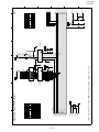
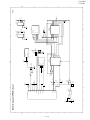
FO-6700U
FO-67DL
SERVICE MANUAL
No. 00ZFO6700USME
FACSIMILE
MODEL FO-6700
OPTION:DUAL LINE KIT
MODEL
FO-67DL
SELECTION CODE
U
DESTINATION
U.S.A.
The FO-6700U Service Manual contains information which differs from the FO-5800U Service Manual.
For additional information, refer to the FO-5800U/C (00ZFO5800USME), FO-4700U/FO47UC (00ZFO4700USME)
Service Manuals.
CAUTION
This laser facsimile is a class 1 laser product that complies with 21CFR 1040.10 and 1040.11 of the CDRH or IEC60825-1 standard.
This means that this machine does not produce a hazardous laser radiation. The use of controls, adjustments or performance of
procedures other than those specified herein may result in hazardous radiation exposure.
This laser radiation is not a danger to the skin, but when an exact focusing of the laser beam is achieved on the eyes retina, there is
danger of spot damage to the retina.
The following cautions must be observed to avoid exposure of the laser beam to your eyes at the time of servicing.
1) When a problem in the Laser Optical Unit has occurred, the whole Optical Unit must be exchanged as a unit.
2) Do not look into the machine with the Main Switch turned on after removing the Toner/Developer Unit and Drum Cartridge.
3) Do not look into the laser beam exposure slit of the Laser Optical Unit with the connector connected when removing and installing the Optical Unit.
4) The cover of Laser Printer Unit contains the Safety Interlock Switch. Do not defeat the safety interlock by inserting wedges or
other items into the switch slot.
Laser Wave Length : 770-810 mm
Laser Pulse Times : 49.2 µs
Laser Output Power : 0.37 mW
Parts marked with " " is important for maintaining the safety of the set. Be sure to replace these parts with specified ones for maintaining the safety and performance of the set.
SHARP CORPORATION
This document has been published to be used
for after sales service only.
The contents are subject to change without notice.
FO-6700U
FO-67DL
CAUTION FOR BATTERY REPLACEMENT
(Danish)
ADVARSEL !
Lithiumbatteri-Eksplosionsfare ved fejlagtig håndtering.
Udskiftning må kun ske med batteri
af samme fabrikat og type.
Levér det brugte batteri tilbage til leverandoren.
(English)
Caution !
Danger of explosion if battery is incorrectly replaced.
Replace only with the same or equivalent type
recommended by the equipment manufacturer.
Discard used batteries according to manufacturer’s instructions.
(Finnish)
VAROITUS
Paristo voi räjähtää, jos se on virheellisesti asennettu.
Vaihda paristo ainoastaan laitevalmistajan suosittelemaan
tyyppiin. Hävitä käytetty paristo valmistajan ohjeiden
mukaisesti.
(French)
ATTENTION
Il y a danger d’explosion s’ il y a remplacement incorrect
de la batterie. Remplacer uniquement avec une batterie du
même type ou d’un type recommandé par le constructeur.
Mettre au rébut les batteries usagées conformément aux
instructions du fabricant.
(Swedish)
VARNING
Explosionsfare vid felaktigt batteribyte.
Använd samma batterityp eller en ekvivalent
typ som rekommenderas av apparattillverkaren.
Kassera använt batteri enligt fabrikantens
instruktion.
(German)
Achtung
Explosionsgefahr bei Verwendung inkorrekter Batterien.
Als Ersatzbatterien dürfen nur Batterien vom gleichen Typ oder
vom Hersteller empfohlene Batterien verwendet werden.
Entsorgung der gebrauchten Batterien nur nach den vom
Hersteller angegebenen Anweisungen.
FO-6700U
FO-67DL
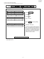
CONTENTS
CHAPTER 1. GENERAL DESCRIPTION
[1] Specifications . . . . . . . . . . . . . . . . . . . . . . . . . . . . . . . . . . . . . . . . . . . . . . . . . . . . . . . . . . . . . . . . . . 1-1
[2] Operation panel . . . . . . . . . . . . . . . . . . . . . . . . . . . . . . . . . . . . . . . . . . . . . . . . . . . . . . . . . . . . . . . . 1-2
[3] Refer to the Service Manual FO-4700U/FO-47UC
[4] Refer to the Service Manual FO-4700U/FO-47UC
[5] Refer to the Service Manual FO-4700U/FO-47UC
[6] Instructions for installing the FO-67DL dual line kit . . . . . . . . . . . . . . . . . . . . . . . . . . . . . . . . . . . . . 1-4
CHAPTER 2. ADJUSTMENTS
[1] Adjustments . . . . . . . . . . . . . . . . . . . . . . . . . . . . . . . . . . . . . . . . . . . . . . . . . . . . . . . . . . . . . . . . . . . 2-1
[2] Diagnostics and service soft switches . . . . . . . . . . . . . . . . . . . . . . . . . . . . . . . . . . . . . . . . . . . . . . . 2-2
[3] Troubleshooting . . . . . . . . . . . . . . . . . . . . . . . . . . . . . . . . . . . . . . . . . . . . . . . . . . . . . . . . . . . . . . . 2-36
[4] Error code table . . . . . . . . . . . . . . . . . . . . . . . . . . . . . . . . . . . . . . . . . . . . . . . . . . . . . . . . . . . . . . . 2-37
[5] Overseas communication mode . . . . . . . . . . . . . . . . . . . . . . . . . . . . . . . . . . . . . . . . . . . . . . . . . . . 2-39
[6] Administrator mode in the personal book function . . . . . . . . . . . . . . . . . . . . . . . . . . . . . . . . . . . . . 2-40
CHAPTER 3. MECHANICAL DESCRIPTION
[1] Refer to the Service Manual FO-4700U/FO-47UC
[2] Refer to the Service Manual FO-4700U/FO-47UC
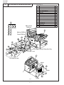
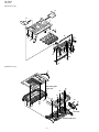
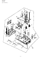
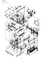
[3] Disassembly and assembly procedures . . . . . . . . . . . . . . . . . . . . . . . . . . . . . . . . . . . . . . . . . . . . . . 3-1
[4] How to install the verification stamp (FO-45VS) refer to the service manual supplement of FO-4700U/FO-47UC
CHAPTER 4. DIAGRAMS
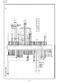
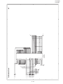
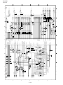
[1] Block diagram . . . . . . . . . . . . . . . . . . . . . . . . . . . . . . . . . . . . . . . . . . . . . . . . . . . . . . . . . . . . . . . . . 4-1
[2] Wiring diagram . . . . . . . . . . . . . . . . . . . . . . . . . . . . . . . . . . . . . . . . . . . . . . . . . . . . . . . . . . . . . . . . . 4-2
[3] Point-to-point diagram and connector signal name . . . . . . . . . . . . . . . . . . . . . . . . . . . . . . . . . . . . . 4-3
CHAPTER 5. CIRCUIT DESCRIPTION
[1] Circuit description . . . . . . . . . . . . . . . . . . . . . . . . . . . . . . . . . . . . . . . . . . . . . . . . . . . . . . . . . . . . . . . 5-1
[2] Circuit description of Main Control PWB . . . . . . . . . . . . . . . . . . . . . . . . . . . . . . . . . . . . . . . . . . . . . 5-1
[3] Circuit description of Line Control PWB . . . . . . . . . . . . . . . . . . . . . . . . . . . . . . . . . . . . . . . . . . . . . 5-16
[4] Circuit description of Memory PWB . . . . . . . . . . . . . . . . . . . . . . . . . . . . . . . . . . . . . . . . . . . . . . . . 5-25
CHAPTER 6. CIRCUIT SCHEMATICS AND PARTS LAYOUT
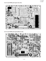
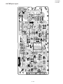
[1] Main Control PWB circuit . . . . . . . . . . . . . . . . . . . . . . . . . . . . . . . . . . . . . . . . . . . . . . . . . . . . . . . . . 6-1
[2] Line-1 Control PWB circuit (FO-6700U) & Line-2 Control PWB circuit (OPTION:FO-67DL) . . . . . 6-19
[3] LIU PWB 1 circuit (FO-6700U), LIU PWB 2 circuit (OPTION:FO-67DL) . . . . . . . . . . . . . . . . . . . . 6-27
[4] Printer PWB circuit . . . . . . . . . . . . . . . . . . . . . . . . . . . . . . . . . . . . . . . . . . . . . . . . . . . . . . . . . . . . . 6-29
[5] Power Supply PWB circuit . . . . . . . . . . . . . . . . . . . . . . . . . . . . . . . . . . . . . . . . . . . . . . . . . . . . . . . 6-33
[6] Operation Panel PWB circuit . . . . . . . . . . . . . . . . . . . . . . . . . . . . . . . . . . . . . . . . . . . . . . . . . . . . . 6-35
[7] High Voltage PWB circuit . . . . . . . . . . . . . . . . . . . . . . . . . . . . . . . . . . . . . . . . . . . . . . . . . . . . . . . . 6-37
[8] Toner Empty PWB circuit . . . . . . . . . . . . . . . . . . . . . . . . . . . . . . . . . . . . . . . . . . . . . . . . . . . . . . . . 6-39
[9] 2nd. Cassette PWB circuit . . . . . . . . . . . . . . . . . . . . . . . . . . . . . . . . . . . . . . . . . . . . . . . . . . . . . . . 6-40
[10] 3rd. Cassette PWB circuit . . . . . . . . . . . . . . . . . . . . . . . . . . . . . . . . . . . . . . . . . . . . . . . . . . . . . . 6-42
[11] Memory PWB circuit . . . . . . . . . . . . . . . . . . . . . . . . . . . . . . . . . . . . . . . . . . . . . . . . . . . . . . . . . . . 6-44
CHAPTER 7. OPERATION FLOWCHART
[1] G3 Protocol . . . . . . . . . . . . . . . . . . . . . . . . . . . . . . . . . . . . . . . . . . . . . . . . . . . . . . . . . . . . . . . . . . . 7-1
[2] Super G3 Protocol . . . . . . . . . . . . . . . . . . . . . . . . . . . . . . . . . . . . . . . . . . . . . . . . . . . . . . . . . . . . . . 7-2
[3] Power ON Sequence . . . . . . . . . . . . . . . . . . . . . . . . . . . . . . . . . . . . . . . . . . . . . . . . . . . . . . . . . . . . 7-3
CHAPTER 8. OTHERS
[1] Service Tools . . . . . . . . . . . . . . . . . . . . . . . . . . . . . . . . . . . . . . . . . . . . . . . . . . . . . . . . . . . . . . . . . . 8-1
[2] IC Signal Names . . . . . . . . . . . . . . . . . . . . . . . . . . . . . . . . . . . . . . . . . . . . . . . . . . . . . . . . . . . . . . . 8-6
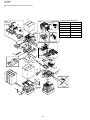
PARTS GUIDE
FO-6700U
FO-67DL
CHAPTER 1. GENERAL DESCRIPTION
[1] Specifications
• GENERAL
Effective Scanning width
10.1" (256 mm) max.
Conventional Auto Dialing:
Rapid Key Dialing: 48 numbers
Speed Dialing: 200 numbers
Personal Auto Dial Books: 30 books
(48 Rapid Keys, 16 Speed Dial numbers
per book)
Effective Printing width
8.0" (203 mm) max.
Reception modes
Auto/Manual
Instascan speed
30 ppm (letter-size documents,
standard resolution)
Memory size*
4 MB (approx. 256 pages)
Full Dual Access
Yes
Modem speed
33,600 bps (max.)
Automatic fallback to lower speeds.
Copy function
Single/Multi/Sort (99 copies/page)
Power requirements
120 V AC, 60 Hz
Transmission time*
Approx. 2 seconds
Operating temperature
50 - 86°F (10 - 30°C)
Humidity
20 to 85% RH
Power consumption
Standby:
Without dual line option: 15 W
With dual line option: 17W
Maximum: 600 W
Dimensions
Width: 18.1" (460 mm)
Depth: 15.4" (390 mm)
Height: 20.1" (510 mm)
Weight
Approx. 55.1 Ibs.(25.0kg)
Automatic dialing
Toner cartridge yield
Initial starter cartridge (included with
(4% page coverage,letter fax machine): Approx. 3000 pages
paper)
Replacement cartridge (FO-47ND):
Approx. 6000 pages
Drum cartridge yield
Resolution
Automatic document
feeder
Paper capacity
Initial starter cartridge (included with
fax machine): 20,000 pages (avg.)
Replacement cartridge (FO-47DR):
20,000 pages (avg.)
Horizontal: 203 pels/inch (8 pels/mm)
Vertical:
Standard: 98 lines/inch (3.85 lines/mm)
Fine /Halftone:
196 lines/inch (7.7 lines/mm)
Super fine:
391 lines/inch (15.4 lines mm)
* Based on ITU-T Test Chart #1 at standard resolution in Sharp special
mode, excluding time for protocol signals (i.e., ITU-T phase C time
only).
Letter paper (20 lb): Max. 50 pages
Legal paper: Max. 20 pages
(Note: 11" x17" paper must be loaded
one page at a time.)
Option
1250 sheets (one 250 sheet tray and
two 500 sheet cassettes)
Toner cartridge
: FO-47ND
Drum cartridge
: FO-47DR
Compression scheme
MMR, MR, MH, JBIG, Sharp (H2)
Option memory
: FO-4ML/8ML/12ML
Halftone (grayscale)
64 levels
Verification stamp
: FO-45VS
Applicable telephone line
Public switched telephone network
Dual line kit
: FO-67DL
Compatibility
ITU-T (CCITT) G3 mode
Printing resolution
Horizontal: 406 lines/inch
(16 lines/mm)
Vertical: 391 lines/inch
(15.4 lines/mm)
Input document size
Automatic feeding:
Width: 5.8 to 10.1" (148 to 256 mm)
Length: 5.0 to 14.3" (128 to 364 mm)
Manual feeding:
Width: 5.8 to 11.0" (148 to 279 mm)
Length: 5.0 to 17.0" (128 to 432 mm)
As a part of our policy of continuous improvement, SHARP reserves the right to make design and specification changes for product
improvement without prior notice. The performance specifications figures indicated are nominal values of production units. There may be some
deviations from these values in individual units.
1–1
FO-6700U
FO-67DL
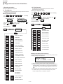
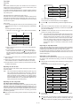
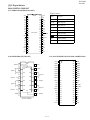
[2] Operation panel
1
Display
This displays messages and prompts during operation and
programming.
2
LINE 1 IN USE light
This lights when the fax machine is using the telephone line.
(If you have installed the dual-line option, this lights when the
fax machine is using Line 1).
3
LINE 2 IN USE light
If you have installed the dual-line option, this lights when the
fax machine is using Line 2.
4
STATUS indicator
This blinks when a paper size error or paper jam occurs. It also
blinks when the print compartment cover is open, or when the
received document tray is not properly installed. A message
appears in the display to indicate the problem.
The indicator lights steadily when a problem occurs which
must be fixed by a service technician.
5
Paper indicator
This blinks when one of the paper sources (tray or cassette) is
out of paper, and lights steadily when all sources are out of paper.
6
Toner indicator
This blinks when the toner cartridge nears empty, and lights
steadily when the toner cartridge needs replacement.
7
Drum indicator
This blinks when the drum cartridge needs replacement.
8
CHANGEOVER key
Two types of information appear in the display: prompts related
to operations you are performing, and information about how
the fax is using the telephone line (transmitting, receiving, etc.).
Press this key to change between the two types of information.
If you have installed the dual-line option, three types of
information appear: prompts related to operations you are
performing, use of Line 1, and use of Line 2.
9
POWER SAVE key
Press this key to turn on Power Save Mode, or set the Power
Save Mode timer if TIMER has been selected with Option
Setting 34 (Power Save Type).
10
RESOLUTION key
Press this key to adjust the resolution before sending or copying
a document.
11
Rapid Dial Keys
Press one of these keys to dial a fax number automatically.
(Note that you must attach the Rapid Key labels.)
12
CONTRAST key
Press this key to adjust the contrast before sending or copying
a document.
13
PAGE COUNTER key
Press this key to include a slash and the total number of pages
after each page number on the pages of a transmitted document.
14
CONFIDENTIAL key
Press this key to send or print out a confidential document.
15
TIMER key
Press this key to set an operation to be performed automatically
at a later time.
16
COVER SHEET key
Press this key to include a cover sheet when sending a fax.
17
LIFE key
Press this key, followed by 1, to check the total number of pages
printed by the fax machine.
2 3
1
LINE 1 IN USE
STANDARD
LINE 2 IN USE
FINE
SUPER FINE
CHANGEOVER
HALF TONE
STATUS
POWER SAVE
4 5
6 7 8
RESOLUTION
9
10
11
01
02
03
04
05
06
07
08
A
B
C
D
E
F
G
H
09
10
11
12
13
14
15
16
I
J
K
L
M
N
O
P
17
18
19
20
21
22
23
24
Q
R
S
T
U
V
W
X
25
26
27
28
29
30
31
32
Y
Z
SPACE
SHIFT
SP
Rapid Key
overlay down
CLEAR
11 12 13 14 15 16 17 18 19
33
34
35
36
37
38
39
40
A
B
C
D
E
F
G
H
41
42
43
44
45
46
47
48
I
J
K
L
M
N
O
P
CONTRAST PAGE COUNTER CONFIDENTIAL TIMER
COVER SHEET
Q
U
R
LINE
Y
S
T
LIFE
V
MEM.STATUS SEARCH DIAL
W
X
DOWN
PERSONAL BOOK
Rapid Key
overlay up
UP
Z
SPACE
SHIFT
SP
CLEAR
21 22 23 24 25
20
28
29 30 31
ABC
1
GHI
4
PRS
7
26
2
JKL
5
TUV
8
OPER
DEF
FUNCTION
COPY
27
32
33
DOCUMENT DUPLEX SCAN
3
MNO
SPEED DIAL
BROADCAST PRIORITY
6
WXY
REPORT
REDIAL
9
SPEAKER
STOP
START
0
34 35 36 37 38 39
40
1–2
FO-6700U
FO-67DL
18
MEM. STATUS key
Press this key to check the status of documents waiting in memory for transmission.
39
START key
Press this key to begin transmission when using Speed Dialing,
Direct Keypad Dialing, or Normal Dialing.
19
SEARCH DIAL key
Press this key to search through your auto dial fax numbers by
name.
40
REPORT key
Press this key to print out a report on the most recently completed transmission or reception.
20
LINE key
If you have installed the dual-line option, press this key to select
the line (Line-1 or Line-2) before dialing.
21
PERSONAL BOOK
Press this key to use or store an auto-dial number in a personal
book. After you press the key, enter the passcode for the book.
22
SPACE key
Press this key to enter a space when programming a name
23
SHIFT key
Press this key to switch between upper and lower case letters
when programming a name.
24
SP key
Press this key to enter a symbol when programming a name.
25
CLEAR key
Press this key to clear a mistake when programming a name or
fax number.
26
Arrow keys
Press these keys to move the cursor forward or backward when
programming a name or fax number.
27
UP and DOWN keys
Press these keys to adjust the volume of the speaker when the
SPEAKER key has been pressed, or the volume of the ringer at
any other time.
28
Dial keypad (numeric keys)
Use these keys to dial and program fax numbers.
29
FUNCTION key
Press this key to select various special functions.
30
SPEED DIAL key
Press this key to dial a Speed Dial number.
31
COPY key
Press this key to make a copy of a document.
32
DOCUMENT key
Press this key to transmit a document without reading it first
into memory.
33
DUPLEX SCAN key
Press this key to transmit or copy a two-sided document.
34
REDIAL key
Press this key to automatically redial the last number dialed.
35
SPEAKER key
Press this key when transmitting a document by Normal Dialing
to listen to the line and verify the response of the receiving fax
machine.
36
BROADCAST key
Press this key to send a document to a group of receiving fax
machines.
37
STOP key
Press this key to cancel an operation before it is completed.
38
PRIORITY key
Press this key when you need to transmit a document ahead of
other documents waiting in memory for transmission.
1–3
FO-6700U
FO-67DL
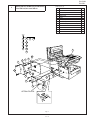
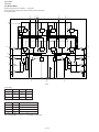
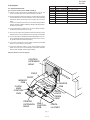
[6] Instructions for installing the FO-67DL dual line kit
The FO-67DL is an option for the Sharp FO-6700
Important!
The following procedure is to be performed by qualified service technicians only.
Be sure to turn off the power, unplug the power cord, unplug the telephone line, and
unplug any extension telephone connected to the unit before proceeding.
1. Open the print compartment cover.
2. Remove the four screws that secure the rear
cover, and then remove the rear cover.
3. Remove the two screws that secure the side
plate, and then remove the side plate.
Side plate
4. Disconnect the cable connector as shown.
Remove the seven screws that secure the large
plate, and then remove the large plate.
5. Insert the bottom edge of the line board into
the slots as shown and then secure the top of
the board with two screws. Connect the cable.
• Use the plastic cable band to bind the cables
together as shown at right.
6. Replace the large plate and secure it with the
seven screws.
• Be sure to insert the top right screw through
the wire ring connector before securing.
Reconnect the cable.
1–4
FO-6700U
FO-67DL
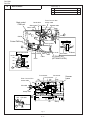
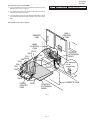
7. Attach the telephone jack plate and secure it
with the two screws.
8. Insert the two plastic bushes into the holes in
the circuit board (insert from the rear side of the
circuit board).
9. Fit the collars over the ends of the bushes to
secure them in the board.
10. Insert the two plastic spacers into the plate as
shown, and then attach the circuit board over
the plate so that the connector on the board
connects to the connector on the plate and the
spacers fit into the holes in the board. Secure
the board with two screws.
11. Replace the rear cover and secure it with the four
screws. Close the print compartment cover.
Note: After installing the dual line option, be sure
to enter the sender’s name and fax number for Line
2 as explained on page 29 of the Operation
Manual.
1–5
FO-6700U
FO-67DL
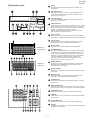
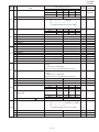
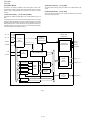
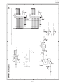
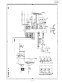
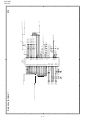
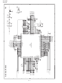
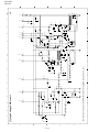
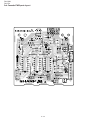
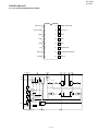
CHAPTER 2. ADJUSTMENTS
2. IC protectors replacement
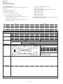
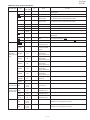
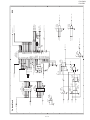
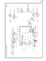
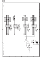
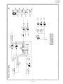
[1] Adjustments
ICPs (IC Protectors) are installed to protect the TX motor drive circuit
and verification stamp drive circuit. ICPs protect various ICs and electronic circuits from an overcurrent condition.
The location of ICPs are shown below:
General
12
1
Since the following adjustments and settings are provided for this model,
make adjustments and/or setup as necessary.
1
CNPW
30
CNSUB2
1
CNPRT
1
50
CNLIU2
50
1. Adjustments
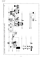
CONTROL PWB
(BOTTOM SIDE)
27 25
Adjustments of output voltage (FACTORY ONLY)
1. Install the power supply unit in the machine.
2. Set the recording paper and document.
3. When the document is loaded, power is supplied to the output lines.
Confirm that outputs are within the limits below.
CNOP
9
IC7
1
CNSP
2
F101
1
F100
CNPN
CNTXM CNSTP
1
MAIN
CONTROL
PWB
1
12
1
CNPW
CN1
CNPRT
30
1
11
1
30
Voltage for adjust
CN1
1
IC2
CN4
PRINTER
PWB
–
8 1
CN7
IC2
VR1
VD
+ Check point for voltage
1
11
CN1
HI VOLTAGE
PWB
–
Fig. 1
Output
+5V MAIN
+5V SUB
+24V MAIN
+24V SUB
Connector
No.
Pin No.
1
11
2
10
3
9
4
8
5
7
6
6
7
5
8
4
9
3
10
2
11
1
Voltage limits
4.845V~5.355V
4.845V~5.355V
23.04V~24.96V
23.04V~24.96V
CN4
CN1
+5V
HV C HL
T VR
T REM
T MON
B MON
B VR
C REM
C MON
MG
+24
ADJUST VOLTAGE LIST
Top Void Printer Adjust Voltage
Label (mm.) Fig. 2
VR1 Fig. 1
5.5~6.9
4.42V
7.0~8.9
3.87V
9.0~10.9
3.14V
11.0~12.9
2.50V
13.0~14.9
1.86V
15.0~17.0
1.22V
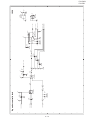
2
1
1
10
Fig. 3
1
8
4 1
CNSEN
24 CNCIS
8
(1) F100 (ICPS10) is installed in order to protect IC’s from and
overcurrent generated in the verification stamp drive circuit. If F100
is open, replace it with a new one.
(2) F101 (ICPS18) is installed in order to protect IC’s from an overcurrent
generated in the TX motor drive circuit. If F101 is open, replace it
with a new one.
In addition to the replacement of F101 and F100, the factor causing
F101 and F100 to open must also be repaired. If not, F101 and
F100 will open again.
Replacement parts
ICPS10 (Sharp code: VHViCPS10//-1)
ICPS18 (Sharp code: VHViCPS18//-1)
CN5
12
1
CNLIU1
50 1
Output voltage settings
POWER SUPPLY
PWB
9
1
CNSUB1
+
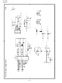
3. Settings
(1) Dial mode selector
Digital multi meter
Connector
No.
Pin No.
1
2
3
4
5
6
7
8
9
10
11
12
CN5
OPTION SETTING: DIAL MODE (Soft Switch No. SW2 DATA No. 1 for
Line-1 and SW32 No.1 for Line-2 with Optional Line Unit)
Use this to set the fax machine to the type of telephone line you are on.
• The factory setting is "TONE".
CNPW
+24V SUB
MG
MG
MG
+24V MAIN
+24V MAIN
+5V SUB
DG
DG
DG
+5V MAIN
+5V MAIN
(step 1) Select "OPTIONAL SETTING".
KEY:
FUNCTION
4
DISPLAY: 4:OPTIONAL SETTING
ENTER #(01-34, ,#)
(step 2) Select "DIAL MODE".
KEY:
2 2
<With optional line unit>
DISPLAY: 22: DIAL MODE
1=TONE, 2=PULSE
22: DIAL MODE
1=LINE-1, 2=LINE-2
Select line using "1" or "2"
Connector
No.
Pin No.
1
2
3
4
5
6
7
8
CN1
KEY:
CN7
24 MAIN
MG
DG
5V MAIN
HEATER ON
FAN
FAN LOCK
H RELAY OFF
DISPLAY: 1: LINE-1
1=TONE, 2=PULSE
KEY:
1
2
DISPLAY: 2: LINE-2
1=TONE, 2=PULSE
(step 3) Select, using "1" or "2".
KEY:
1
DISPLAY: TONE SELECTED
KEY:
2
DISPLAY: PULSE SELECTED
(step 4) End, using the "STOP" key.
KEY:
TOP VOID LABEL
Fig. 2
2–1
STOP
FO-6700U
FO-67DL
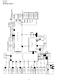
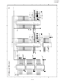
[2] Diagnostics and service soft switches
1. Operating procedure
1-2. Print diagnosis
Two kinds of diagnoses are supported.
This diagnosis is concerned with the print which is used for
production and service support.
1-1. Fax diagnosis
Entering the diagnostic mode
This diagnosis is concerned with the main body of fax which is used
for production and service support.
9
Press FUNC
display will appear.
Entering the diagnostic mode
9
Press FUNC
display will appear.
8
Without Optional Line Unit
MAIN:
SUB:
7 , and the following
MAIN:
SUB:
FBQ0
FEF0
6 , and the following
PCU ROM Ver.:
Then press the START key. Select the desired item with
key and the
key or select with the rapid key.
With Optional Line Unit
FBQ0
FEF0
8
the
Enter the mode with the START key.
FEF0
(Diag • specifications)
Then press the START key. Select the desired item with the
and the
key or select with the rapid key.
Enter the mode with the
key
FUNC
9
8
6
PCU ROM Ver.:
START key.
(Diag • specifications)
START
9
FUNC
8
7
ROM: FBQ0
ROM: FEF0
START
01
START
AREA PRINT MODE
02
START
CHECK PATTERN 1
03
START
CHECK PATTERN 2
04
START
CHECK PATTERN 3
05
START
PAPER FEED AGING
06
START
BIAS ADJUST MODE
07
START
LIFE SET MODE
08
START
LIFE ALL CLEAR
09
START
LIFE ENTRY MODE
10
START
TOP ADJUST MODE
11
START
LIFE CLEAR MODE
01
START
SOFT SWITCH MODE
02
START
PRINT AREA
03
START
ROM & RAM CHECK
04
START
AUTO FEEDER MODE
05
START
AGING MODE
06
START
PANEL CHECK MODE
07
START
OPTICAL ADJUST MODE
08
START
PRODUCT CHECK
09
START
SIGNAL SEND MODE
10
START
COMM. CHECK MODE
11
START
MEMORY CLEAR MODE
12
START
FLASH MEMORY CHECK
13
START
ALL FAX/TEL. ENTRY MODE
14
START
DEPT. PASSCODE
15
START
CONF. PASSCODE
16
START
PRINT HOLD CODE
17
START
MEMORY SET MODE
18
START
STAMP AGING
1 = All the data will be deleted including initially registered data.
2 = Delete the image file to be used in transmission. This will delete all
the data related to communication such as reserved transmission or
intercepting. However, the data initially registered will not be deleted.
19
START
DIAL TEST MODE
3 = Memory will not be cleared and the machine enters stand-by mode.
20
START
COPY DIAG MODE
Memory clear when power is turned on
21
NO FUNCTION
22
NO FUNCTION
23
START
SIGNAL SEND 2 MODE
24
START
JBIG TEST MODE
25
START
PERSONAL BOOK LST
Pressing the START and STOP keys, turn on the main power, and the
following message will be displayed.
MEMORY CLEAR ?
1 = ALL , 2 = IMAGE , 3 = NO
• "2 = IMAGE" memory clear is done automatically, when power is
turned on after FO-67DL is installed or removed.
2–2
FO-6700U
FO-67DL
2. Diagnostic items description
•
2-1. Fax diagnosis
1) Soft switch mode
In this mode, the soft switch are set and the soft switch list is printed.
Soft switch mode screen
SOFT SWITCH MODE
SW01=00000000
•
•
Switch 1 2 3 4 5 6 7 8 :DATA No.
No.
Data
1 Switch number selection
•
•
•
Press START key for setting of the next soft switch. If the soft
switch number is the final, pressing START key will exit the soft
switch mode.
Enter two digits of a soft switch number to set the switch number.
If a switch number of unexisting soft switch is entered, key error
buzzer sounds to reject the input.
ENTER LAST DIGIT
SW1
SOFT SWITCH MODE
SW01=00000000
1
SOFT SWITCH MODE
SW16=00010110
•
7 Linked change of data (This is the same even in the optional setting.)
6
2 Data number selection
•
The cursor position shows the data to be set.
Pressing # key moves the cursor to the right. If, however, the cursor is
on data number 8, pressing # key shifts the cursor to data number 1
of the next switch number. If the switch number is the final, pressing
# key will exit the soft switch mode.
Pressing key moves the cursor to the left. If, however, the cursor is
on data number 1, pressing key shifts the cursor to data number 1
of the former switch number. If the switch number is 1, pressing
key will not move the cursor and the error buzzer will sound.
When the department control function is off, the multi TTI function and telephone billing code function are turned off.
2) Print area
According to the size of the specified sheet, the effective printing area is
printed.
3) ROM & RAM check
3 Data setting method
No.
Press the FUNCTION key, and the data at the position of the cursor
will be reversed to 0 when it is 1, or to 1 when it is 0. (If the soft switch
can be changed at the bit (Refer to .), the error buzzer will sound
with the process not received.)
4 Outputting method of soft switch list
OFF to ON of telephone billing function which is using the image
memory is used (Note: In the existing set, the telephone billing
code function is specified from OFF to ON when the timer system
communication (including the batch communication) is set.)
Here, the memory is usable when the telephone billing code function is on. It can be set from ON to OFF while the memory is
used. However, if setting is practically changed even once, it can
not be returned from OFF to ON.
Switching ON/OFF of PC interface function during the use of image memory.
OFF to ON of department control function during use of image
memory.
(Note: In the existing set, the department control function is set
from OFF to ON when the timer communication (including the
batch sending) or the memory hold is set.)
ON to OFF of continuous serial polling function when the continuous serial polling is started.
(Note: In the existing set, "ON to OFF of the continuous serial
polling function when the continuous serial polling is registered"
has been applied, but the conditions are now moderated. However, registration is impossible to the program of the new continuous serial polling when the continuous serial polling function is
OFF.)
In addition, change of all soft switches during communication
Device checked
1
6
2
3
In the soft switch mode, press the REPORT key, and the soft switch
list will be output.
If the recording paper runs out or is clogged, the key error buzzer will
sound with the process not received.
Remarks
<Short sound>:
Integrated ROM <Short sounds> 2 times 0.5 sec.ON / 0.5 sec.OFF
SRAM
<Short sounds> 3 times <Long sounds>:
D-RAM
<Short sounds> 4 times 1.0 sec.ON / 0.5 sec.OFF
5
ROM
<Long sound> 1 time
6
Integrated ROM <Long sounds> 2 times
Sub1
D-RAM
<Long sounds> 3 times
8
Dual port RAM
<Long sounds> 4 times
9
ROM
<Long sounds> 5 times
10
In the following case, the data of the soft switches set will be stored.
• It is shifted to set the next soft switch by pressing the START
switch.
• It is shifted to set the next soft switch with the [#] key.
• It is shifted to set the last soft switch with the [ ] key.
• It is shifted to set another soft switch by inputting two digits as the
switch number. (When 2 digits are completely input.)
• Output of the soft switch list is started.
Main
<Short sound> 1 time
4
7
5 Storage of data
Number of buzzer sound
ROM
11
Sub2
12
Integrated ROM <Long sounds> 6 times If the sub-2 PWB is not
D-RAM
<Long sounds> 7 times installed, error buzzers
Dual port RAM
<Long sounds> 8 times will not go off.
<Without Optional Line Unit>
6 Inhibition of data change
ROM CPU SRAM DRM DPR
ROM CPU SRAM DRM DPR
••
PP
••
•
••
•
PP
P
EP
P
<With Optional Line Unit>
(This is also applicable for the optional setting.)
In the following case, it is inhibited to change the data with the key
error buzzer.
• Switching ON/OFF of ECM during the use of image memory.
• Switching OFF to ON of the print hold function when the print
hold pass code has not yet been registered.
• Clearing the print hold pass code when print hold function is ON.
• Switching ON/OFF of the print hold function during the use of
memory such as in the case of substitute receiving.
2–3
ROM CPU SRAM DRM DPR
ROM CPU SRAM DRM DPR
•••
PPP PPP P
•••
•
•••
••
EPE PP
FO-6700U
FO-67DL
4) Auto feeder mode
7) Optical adjust mode
The auto feed function can be checked by inserting and discharging the
document. (The distance between pages can be displayed during operation of the scanner.)
Check of auto feed function
After this mode is activated, set up the document, and press the
START key, and it will be automatically fed. (Before the START key is
pressed, the document sensor alone is activated.) Moreover, the
document size (A4/B4) and sensor information (A4/B4/ORG) are displayed when the document sensor is turned.
When this mode is executed, the reading LED will be lit. This will go out
if the STOP key is pressed.
1
8) Product check
The diagnosis is used in the production process.
After shift to the mode, the following operations are sequentially executed. At this time, the sensor of read-error can be checked by feeding
the B4 document. Set up one short document of B4 size.
1 Memory clear (Same as Diagnosis 11)
2 Panel test (Same as Diagnosis 06)
3 Dial test (Same as Diagnosis 24)
4 Document auto feed
5 ROM & RAM test check (Same as the Diagnosis 03)
6 Flash memory test mode (Same as Diagnosis 12)
7 Registration of fixed data
04 : AUTO FEEDER MODE
After setup of the document
04 : AUTO FEEDER MODE
B4 (A4 B4 ORG)
Only the sensor which is
activated (fallen down) is displayed.)
The paper sheet size (A4/B4) is
displayed.
2 Display of distance between pages during operation of the scanner
•
•
•
•
Registration of rapid key No. and other data necessary for production.
The registered data are shown in the following table. The chain dial
is not set for any destination.
Soon after this mode is activated, press the FUNCTION key for 5
seconds or more, and the display mode of the distance between
pages will be activated. Then, set up the sending paper and select
the image quality, and then press the START key, and operation
will be started.
Be sure to press the FUNCTION key prior to the START key. If
the FUNCTION key is not pressed but the START key is pressed,
it will operate in the same matter as in the existing auto feeder
mode.
If the START key is pressed, the FUNCTION key will be invalid
hereafter. Therefore, the display mode of the distance between
pages and the existing mode can not be changed.
While the sending paper is read, the image quality key can be
input. STD/FINE/S-FINE modes are usable. However, the same
operation of FINE will be selected if the intermediate tone is set.
The image quality, the length of the sending page read, the page
distance to the next sending paper and the total of the sending
papers read are shown on the display.
When the stop key is pressed or 100 sending papers are read,
the content shown on the display will be totally output as the list
after the remaining sending papers are discharged.
Rapid
No.
01
FAX
No.
20
Rapid
No.
06
FAX
No.
25
Rapid
No.
11
FAX
No.
1
Rapid
No.
21
FAX
No.
01
02
21
07
26
12
2
22
02
03
22
08
27
13
3
23
03
04
23
09
28
14
4
24
04
05
24
10
29
15
5
25
05
8 Transmission check (Same as Diagnosis 10)
The soft switches necessary for production are set.
9 Test result print (one sheet)
Memory clear printing
Panel test result printing
ROM & RAM test result printing
F Print area printing (one sheet)
5) Aging mode
If any document is set up in the first state (when started), copying will be
executed. If it is not set up, "check pattern 1" of the print diagnosis is
output at the intervals of 1 time/60 minutes. (A total of 10 sheets are
output.)
6) Panel check mode
This is used to check whether each key is normally operated or not.
According to the key input, LCD is displayed. Moreover, during execution,
the document reading lamp is turned on.
Test results are printed. (The maximum 100 input keys can be printed .)
LED repeats lighting at regular intervals in sequence. (Lighting speed
is specified separately.)
In case of inputting all keys, key input OK is displayed when finishing
the STOP key.
When pressing the NUMERIC key during panel check, output of DTMF
corresponding with the key is started.
When pressing other keys, output is stopped.
2–4
FO-6700U
FO-67DL
4 If any chain dial is not in the Rapid number, the Rapid numbers 02
9) Signal send mode
After shift to the mode, press the START key, and the signals will be
transmitted in the following sequence.
It can be used to check the modem and so on.
thru 48 and SPEED key numbers 001 thru 200 are registered in the
group number 01.
If any chain dial is set, the group will be not produced but the chain
dial setting alone of the Rapid number 01 will be reset.
(In all others except the Rapid number 01, the chain dials will be
continuously set as they are.)
[ 1] No signals
[ 2] 4800BPS (V27ter)
[ 3] 14400BPS (V. 33)
Rapid key
RXX
SPEED key SXXX
[ 4] 12000BPS (V. 33)
XX : Rapid number
XXX : Speed key number
[ 5] 14400BPS (V. 17)
(16th and subsequential letters of the destination name registered in the
Rapid number 01 will be discarded.)
[ 6] 12000BPS (V. 17)
5 Personal book 00 to 30 are set up. (Their PASSCODE to be regis-
[ 7] 9600BPS (V. 17)
[ 8] 7200BPS (V. 17)
tered are 0000 to 0030, and the NAME are "BOOK00" to "BOOK
30".)
[ 9] 9600BPS (V. 29)
6 The registration information of RAPID01 is copied to RAPID02 to 48
of each book.
7 The registration information of RAPID01 is copied to SPEED001 to
016 of each book.
8 When the chain dial is not set up in RAPID01, specify RAPID02 to 48
[10] 7200BPS (V. 29)
[11] 4800BPS (V27ter)
[12] 2400BPS (V27ter)
[13]
300BPS (FLAG)
and SPEED001 to 016 in GROUP1 of each book.
[14] 2100Hz (CED)
14) Dept. passcode
[15] 1100Hz (CNG)
The department passcode list is printed.
10) Comm. check mode
1 Turn on the Line Monitor.
2 Turn off the Cover Sheet Function.
3 Set Line Equivalence at 0 km.
15) Conf. passcode
After the check, it is necessary to be sure to return the aforementioned
soft switches into the initial state.
(Clear the memory with the diagnosis.)
The print lockout passcode No. is printed.
The confidential passcode list is printed.
Differing from printing of one box alone soon after registration, the confidential passcodes of all boxes are printed.
16) Print hold code
17) Memory set mode
The set and dump list of the memory content is output.
11) Memory clear mode
Clear the back-up memory to initialize the soft switches.
The Flash Memory will be initialized. Then, the initialized list be output.
•
The address (8 digits (P) generally including the bank information is
input, and the data of 2 digits is continuously input.
Inputting is done in the hexadecimal mode. The ten-key is used for 0
thru 9, and the alphabetic keys A (RAPID 01 thru 06) are used for A
thru F.
•
During data inputting, the address can be moved forward and backward one byte by one byte with " " and "#". (The address prior to the
address 0 is looped as the maximum address.)
•
The Validity of the address is not checked. Accordingly, writing/ reading operations are possible in the address of the memory not assigned, the address of ROM and so on.
(However, as practical, writing is not done, and the data content runs
short each reading.)
Though writing is possible in the flash memory, a little time is required.
It is also necessary to take care that the life of the flash memory is
excessively shortened if much data is written in the flash memory.
Since it may run away depending the written content, take minute
care for the writing address.
•
When the REPORT key is input, the memory dump list is produced
from the displayed address (here, it is limited at the 16-byte boundary address (address with end 0) which does not exceed the specified address and is just in front.). The dump list is output to a maximum of 99 pages. If any data of one page can be repeatedly developed and printed, the list is sufficient. But it is not desired that the
content of plural pages are developed in the memory once and are
then printed. If the STOP key is pressed, it will pass to the diagnosis
after the page which is now being printed is completed printed.
If the address exceeds the maximum address, it will return to the
address 0 and printing will be continued.
12) Flash Memory check
The Flash Memory is checked.
The ordinary memories (ROM, SRAM, DRAM) are checked in the ROM
& RAM check process. The write/read test is taken every block to print
the result.
When an error occurs, the following error buzzer will sound.
Number of buzzer sounds
9 times <Short sounds>
Check device
Flash memory (Option)
During operation of this diagnosis, dual operation is not possible at all.
If this is excessively repeated, it will shorten the life of the flash memory.
13) All FAX/TEL. entry mode
The function is used to simplify the registration of FAX/TEL No. during
aging.
1 The diagnosis mode is activated. If anything is not registered in the
Rapid number 01 or any program or group is not registered, it will
pass the diagnosis without doing anything.
2 The FAX/TEL number (including the substitutive destination) of the
Rapid number 01 is copied to the Rapid numbers 02 thru 48.
3 FAX number of the Rapid number 01 is copied to SPEED key numbers
001 thru 200.
18) Stamp aging
Diag mode is left though it doesn’t have this function.
2–5
FO-6700U
FO-67DL
19) Dial test mode
23) Signal send mode 2
The mode is used to inspect whether dialing is accurate in two kinds of
dial modes . All data which can be dialed in this mode are automatically
called up in both PB mode and DP mode.
The signals concerned with V.34 & V.8 are checked.
After this mode is activated, press the START key, and the signals will
be sent in the following sequence.
It can be used to check the modem.
When this mode is activated, the following operations will be automatically executed . Whether the dialed content is right or not is judged with
the external instrument which is connected to the line cable.
[ 1] No signal
1 After shift to the FAX diagnosis mode, press RAPID 24.
(Also switch the display with the [ ] and [#] keys.)
2 Press the START key.
3 Turn on CML, and dial the following in the PB mode.
1, 2, 3, 4, 5, 6, 7, 8, 9, , 0, #
4 Turn off CML 500 mS alone.
5 Dial the following in the DP mode.
1, 5, 9, 0
6 After dialing, turn off CML.
[ 2] 33600BPS
[ 3] 31200BPS
[ 4] 28800BPS
[ 5] 26400BPS
[ 6] 24000BPS
[ 7] 21600BPS
[ 8] 19200BPS
[ 9] 16800BPS
This mode uses the ordinary auto dial. (Accordingly, the signal sending
time and minimum pause are all the same as ordinary.
The measurement result in this mode is completely all the same as in
the ordinary dial mode.
Moreover, the same process as above is also done in the dial test mode
which is executed in the product check mode.
[10] 14400BPS
[11] 12000BPS
[12] 9600BPS
[13] 7200BPS
[14] 4800BPS
20) Copy diag mode
[15] 2400BPS
In order to shorten the process time during production, this mode is
used to automatically switch the copy mode. Three menus are provided.
1.
1 Set up two documents. (In case of two documents or more,
1 Enter the diagnostic mode.
2 Press the RAPID24 button. ("24: JBIG TEST MODE" appears.)
3 Press the START key to begin the JBIG test operation.
24) JBIG test mode
there is no problem.
2 Press the START key.
3 Copy 1st document in the fine mode/density AUTO. (One sheet
When both tests are completed normally, the buzzer sounds and "JBIG
TEST NORMAL END" appears at the same time.
If the decoding test terminates abnormally, the buzzer sounds and
"ERROR: JBIG DECODE" appears at the same time.
If the encoding test terminates abnormally, the buzzer sounds and
"ERROR: JBIG ENCODE" appears at the same time.
is printed in the ordinary copy mode.)
4 Copy 2nd (subsequential) document in the intermediate tone
mode/density DARK. (In the ordinary copying mode, one sheet
is printed when the RESOLUTION key is pressed three times.)
When copy test is tried during production or is checked in two modes
(fine and intermediate tones), this mode is provided to reduce the troublesome work which makes the operator stand aside to change the mode.
Accordingly, the fine and intermediate tones are merely switched, and
the mode is not switched to another mode. (Input of the image quality/
density key is invalid.)
25) Personal book list
The PASSCODE of the personal book 00 to 30 are output.
2. Try the copy in the mode fixed at COPY REDUCE 95% and fine
mode/density AUTO. At this time, don’t change the soft key of
COPY REDUCE. (Input of the image quality/density key is invalid.)
3. Continuously try the above items 1 and 2.
21) No function
22) No function
2–6
FO-6700U
FO-67DL
Rapid key 05: Paper feed aging
2-2. Print diagnosis
The mode is used for aging related to the printing. In this mode, the
following modes are provided.
Blank paper aging mode (ALL WHITE AGING)
Whole black print aging mode (ALL BLACK AGING)
4% printing aging mode (4% AGING)
After selecting the paper-pass aging mode in the print diagnosis mode,
input the number of each mode above with the ten-key, and the mode
will be executed. The detailed specifications of each mode are described
as follows. Here, the operation in each mode is stopped only when the
STOP key is pressed by the operator or a printing-impossible error occurs.
Rapid key 01: Area print mode
1
2
3
The effective printing area frame is printed in the specified sheet size.
4mm ± 2.5
1
2
3
4
5
6
7
8
9
4mm
•
Blank paper aging mode
In the mode, printing is continued in the whole white (white paper)
printing pattern until the STOP key is pressed by the operator. (In the
printing area)
•
Whole black printing aging mode
In the mode, printing is continued in the whole black (whole black)
printing pattern until the STOP key is pressed by the operator. (In the
printing area)
208mm
4mm ± 2
4mm
1. [Full black pattern]
2. [Intermediate tone 2 pattern]
The left pattern is repeated.
Rapid key 06: Bias adjust mode
The mode is used to adjust the printing density of the printed image. The
image printing density is adjustable in seven steps of 1 to 7.
For details, refer to the following table. (For selection, use the keys 1
thru 7.)
Image printing density
3. [Intermediate tone 1 pattern]
The left pattern is repeated.
Thin
←
1
2
3
4
5
→
Thick
6
7
Default value
Rapid key 07: Life set mode
The mode is used to set the life counter of the printer and the counter of
the auto feeder at desired values. For setting, proceed with the following
procedure.
1 When the life counter setting mode is selected, the following will be is
displayed.
4. [Mesh point pattern]
The left pattern is repeated.
M A C H I N E
L I F E = 0 0 0 1 2 3
D R U M
L I F E = 0 0 0 1 2 3
L I F E 1 = 0 0 0 1 2 3
key
# key
L I F E 2 = 0 0 0 1 2 3
5. [Longitudinal strip 2 pattern]
Black 2 dot and white 2 dot are repeated in line.
6. [Lateral strip 2 pattern]
Black 2 line and white 2 line are repeated.
L I F E 3 = 0 0 0 1 2 3
7. [Longitudinal strip 1 pattern]
Black 1 dot and white 1 dot are repeated in line.
F E E D E R
L I F E = 0 0 0 1 2 3
8. [Lateral strip 1 pattern]
Black 1 line and white 1 line are repeated.
9. [Full White pattern]
The cursor blinks at the top data.
Five counters can be selected with the "#" and " " keys.
Rapid key 02: Check pattern 1
2 In the state 1, input a desired setting number of 6 digits with the tenkey.
3 After input of 6 digits, shift to another counter with the "#" and " "
The lateral stripe 2 pattern is printed on one sheet.
(Black 2 line and white 2 line are repeated.)
Rapid key 03: Check pattern 2
The lateral stripe 2 pattern is printed on multiple pages.
Press the STOP key to end the printing.
keys as necessary. When all necessary counters are completely input, press the START key.
4 "STORED" will be displayed with the set values stored into the memory.
Rapid key 04: Check pattern 3
The intermediate tone 1 is printed on one sheet.
For checking, retry this mode.
2–7
FO-6700U
FO-67DL
Note:
This counter indicates the printer use conditions such as numbers of
printed pages from the beginning of use. In the normal memory clear
condition, the counter will not be reset.
In conditions including damaged memory contents caused by repairing
the panel, this counter should be reset or cleared in addition to the ordinary memory clear.
L I F E 1 = 0 0 0 0 0 0
# key
L I F E 2 = 0 0 0 0 0 0
key
L I F E 3 = 0 0 0 0 0 0
Operation Manual for multipurpose Counter Life 1-3
The FAST function of LIFE 1-3 automatically notifies the dealer that the
printer life has reached the optional judgement value. This function can
be applied to notify when the life of consumables such as the printing
unit and fixer is expired.
The cursor blinks at the top data.
Three counters can be selected with the "#" and " " keys.
2 In the state 1 , input a desired setting number of 6 digits with the tenkey.
3 After input of 6 digits, shift to another counter with the "#" and " "
How to use it
(1) Set the optional judgement value (counter value for alarming) of the
multipurpose life counter 1-3 in the printer diagnotor 09: LIFE ENTRY
MODE.
keys as necessary. When all necessary counters are completely input, press the START key.
The setting procedure is as follows:
1. Select each counter with " " or "#" key. (Refer to the chart below.)
4 "STORED" will be displayed with the set values stored into the
memory. For checking, retry this mode.
Note:
L I F E 1 = 0 0 0 0 0 0
# key
L I F E 2 = 0 0 0 0 0 0
key
L I F E 3 = 0 0 0 0 0 0
The counter shows the operational state of the printer (how many
sheets have been printed since start of use? and others). The
ordinary memory does not reset the counter. Accordingly, it is
necessary to reset the counter or do the clear process in addition to the ordinary memory clear if the content in the memory
on the control PWB is broken because of PWB repair, etc. (In
the production stage, it is necessary to execute this in the last
process.)
Rapid key 10: Top adjust mode
As the method to adjust the top margin for printing, adjust top margin
adjusting VR on the PWB. If this mode is used at this time, adjustment is
possible without the printing test every time when VR is turned.
For the practical use, determine the adjusting value on the basis of the
old data, and adjust to the determined value in this mode. Then, check it
with the printing test.
2. Enter 6 digits using the ten key on the screen of the judgement
value to be set.
3. If another value is to be set after completion of the first entry,
move onto another value with "#" or " " key and enter digits in
the same procedure. Press the "START" key when all values are
entered. (Writing is completed when "STORED" appears on the
display.)
Rapid key 11: Life clear mode
(2) The counter whose value is set in (1) will start counting every time a
letter is printed.
(3) When each counter reaches its judgement value, the FAST auto
matic notification function is activated and alarms it to the dealer.
The mode is used to respectively clear the life counter of the printer and
the counter of the auto feeder. For setting, proceed with the following
procedure.
1 When the life counter clearing mode is selected, the following will be
• If the FAST function is off, the counter only counts and does not notify
is displayed.
Seven counters can be selected with the "#" and " " keys.
the dealer automatically.
Rapid key 08: Life all clear
The mode is used to clear the life counter of the printer of the counter
of the auto feeder.
Note:
The counter shows the operational state of the printer (e.g. how
many sheets have been printed since start of use?). The ordinary memory does not reset the counter. Accordingly, it is necessary to reset this counter in addition to the ordinary memory
clear if the content in the memory on the control PWB is broken
because of PWB repair, etc. (In the production stage, it is necessary to execute this in the last process.)
M A C H I N E
L I F E
C L E A R
D R U M
L I F E
C L E A R
L I F E 1
C L E A R
L I F E 2
C L E A R
L I F E 3
C L E A R
F E E D E R
L I F E
C L E A R
T O N E R
L I F E
C L E A R
# key
key
Rapid key 09: Life entry mode
(For Serviceman temporary counter)
The mode is used to set a desired value for the judgment value (alarm
judgment counter value) of the general purpose life counters 1 thru 3 of
the printer. If the life of a consumable part (developer, imprinter, etc) is
set, the model which has the error display and RMS function will inform
RMS when the counter reaches the set value. For setting, proceed with
the following procedure.
1 When the life counter setting mode is selected, the following will be
2 In the state 1, input the CLEAR key, and the counter will be respectively cleared.
3 After one clear, move the cursor to another counter with the "#" and
displayed.
" " keys as necessary, and then press the CLEAR key. When the
necessary counters are completely cleared, press the STOP key.
2–8
FO-6700U
FO-67DL
3. How to make soft switch setting
To enter the soft switch mode, make the following key entries in sequence.
Press FUNCTION
9
8
7
START
01
START
SFT S W 1 = 0 0 0 0 0 0 0 0
Press FUNCTION key.
SFT S W 1 = 1 0 0 0 0 0 0 0
Press
key.
Press
key.
SFT S W 1 = 1 0 0 0 0 0 0 0
SFT S W 1 = 1 0 0 0 0 0 0 0
Bit1 - 8 are set.
SFT S W 1 = 1 0 0 0 0 0 0 0
Press START key during setting.
SFT S W 2 = 0 0 0 0 0 0 0 0
Soft SW2 - 99 are set.
S F T S W 99 = 0 0 0 0 0 0 0 0
To finish the settings halfway between
SW 1 and SW99, press the STOP key.
In this case, the setting being done to
the SW No. on display will be nullified
while settings done to the preceding
SW Nos. remain in effect.
The soft switch mode is terminated.
•
•
SW1 to SW30 : For line 1
SW31 to SW60 : For line 2
2–9
FO-6700U
FO-67DL
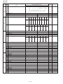
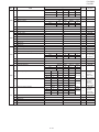
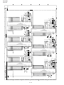
4. Soft switch description
• Soft switch
SW DATA
NO. NO.
SW1
SW2
SW3
SW4
SW5
1
2
3
4
5
6
7
8
1
2
3
4
5
6
7
8
1
2
3
4
5
6
7
8
ITEM
Recall interval
Recall times
Dial mode
Receive mode
ECM mode
Reserved
Polling security
Auto cover sheet
JUNK-FAX function in manual reception
JUNK-FAX function
Number of rings for auto-receive
(0: No ring receive)
Switch setting and function
1
0
Binary input
8 4 2 1
No. =
1 2 3 4 (Data No.)
EX
0 1 0 1
eg. Recall interval is set to 5 min.
Binary input
8 4 2 1
No. =
5 6 7 8 (Data No.)
EX
0 0 1 0
eg. Recall times is set to 2 times.
PULSE
TONE
AUTO
MANUAL
Off
On
5
6
7
8
On
Off
No
Yes
Yes
No
Yes
No
Binary input
8 4 2 1
No. =
1 2 3 4 (Data No.)
EX
0 0 0 1
eg. Number of rings for auto receive is set to 1 time.
Switch to auto-receive from manual receive
Binary input
8 4 2 1
(0: No switch)
No. =
5 6 7 8 (Data No.)
EX
0 0 0 0
eg. Switch to auto receive is set to disable.
Communication results printout
Printed at Printed at Printed at Not printed Printed
error only error/timer/ transmisevery time
memory sion mode
only
only
No. 1
0
0
0
1
1
No. 2
0
0
1
0
1
No. 3
1
0
0
0
0
Image addition function to the communication On
Off
result table (for memory transmission only)
Reserved
TEL billing code function
On
Off
Billing code position
Before
After
Multi-TTI feature
On
Off
1
2
3
4
5
6
7
8
Time display format
Date display format
Header print
Footer print
Relay data output
Substitute reception
Substitute reception conditions
CSI transmission
1
2
3
4
24 hours
Month-Day-Year
Off
On
No
Off
Reception disable without TSI
Off
2 – 10
12 hours-AM/PM
Day-Month-Year
On
Off
Yes
On
Reception enable without TSI
On
Initial
setting
0
1
0
1
0
0
1
0
0
1
0
0
1
1
0
0
0
0
0
1
0
0
0
0
Remarks
OPTION
Set to 1~15
OPTION
Set to 0~14
OPTION
OPTION
OPTION
OPTION
OPTION
Set to 0~9
OPTION
Set to 0~9
OPTION
0
0
1
1
OPTION
0
0
1
0
OPTION
OPTION
OPTION
0
1
0
0
0
0
0
0
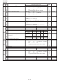
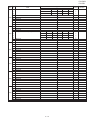
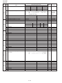
FO-6700U
FO-67DL
SW DATA
NO. NO.
1
2
3
4
SW6
Switch setting and function
ITEM
JBIG (Joint Bi-level Image Group)
JBIG option
MMR
MR
Modem speed
5
6
7
8
1
On
On
On
On
No. 5
No. 6
No. 7
No. 8
Reception speed fixed
1
2
3
DIS receive acknowledge during
G3 transmission
Twice
4
Non-modulated carrier in V.29
On
5
6
7
8
transmission mode
CNG send when manual TX
Protocol monitor
Line monitor
Max. length for TX/RX/Copy
Compromised equalizer
0
Off
Off
Off
Off
V.33
V.17
V. 29
V. 27ter
14400 12000 14400 12000 9600 7200 9600 7200 4800 2400
0
0
1
1
1
1
0
0
0
0
1
1
0
0
0
0
0
0
0
0
0
1
0
1
0
1
0
1
1
0
0
0
0
0
1
1
1
1
0
0
NO
V. 17V. 29- V. 27ter14400bps 9600bps 4800bps
No. 1
0
1
0
1
No. 2
0
1
1
0
Once in NSF reception, twice
in DIS reception
Initial
setting
1
0
1
1
1
0
0
0
0
0
0
SW7
SW8
1
2
3
4
5
6
7
8
H2 mode
Signal transmission level
Off
On
Off
On
Off
On
Off
TX: unlimited, RX: unlimited
TX/Copy: 1.0m, RX: 1.5m
0Km
1.8Km
3.6Km
7.2Km
No. 1
0
0
1
1
No. 2
0
1
0
1
No
Yes
Binary input
16 8 4 2 1
No. =
4 5 6 7 8 (Data No.)
EX
0 1 1 0 1
eg. Signal transmission level is set to -10dBm
CED tone signal interval
SW9
1
2
3
4
5
6
7
8
No. 1
No. 2
Equalizer freeze
Equalizer freeze conditions
CED detection time
Alarm buzzer
Action when RTN received
75ms
0
0
On
All
500ms
No. 5
No. 6
Handle to error
2 – 11
3sec
0
0
500ms
750ms
1000ms
0
1
1
1
0
1
Off
7200bps
1000ms
1sec
No BEEP No BEEP
0
1
1
1
0
1
Handle to no error
Remarks
When 14400bps
MODEM used,
setting to
14400bps is
ignored.
Effective to
international
comm.
0
1
0
0
0
0
0
0
0
1
1
0
1
0
0
0
0
0
0
0
0
Valid when
transmitting
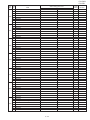
FO-6700U
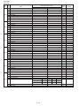
FO-67DL
SW DATA
NO. NO.
SW10
SW11
SW12
SW13
SW14
1
2
3
4
5
6
7
8
1
2
3
4
5
6
7
8
1
2
3
4
5
6
7
8
1
2
3
4
5
6
7
8
1
2
3
4
5
6
7
8
ITEM
Memory retransmission times
Memory retransmission interval
Switch setting and function
1
0
Binary input
8 4 2 1
No. =
1 2 3 4 (Data No.)
EX
1 0 1 0
eg. Retransmission time set to 10 times.
Binary input
8 4 2 1
No. =
5 6 7 8 (Data No.)
EX
0 0 1 0
V.34 mode transmission speed
Sending speed = 2400 (bps) x N
Example :
2400 (bps) x 12 = 28800 (bps)
2400 (bps) is set for N=0. 33600 (bps) is set for N=15.
V.34 mode receiving speed
Receiving speed = 2400 (bps) x N
Example :
2400 (bps) x 12 = 28800 (bps)
2400 (bps) is set for N=0. 33600 (bps) is set for N=15.
V.34 mode function in case of manual communication On
Off
V.34 mode function
On
Off
V.34 control channel communication speed
2400bps
1200bps
EOL detection timer
13sec
25sec
5sec
5sec
No. 4
0
0
1
1
No. 5
0
1
0
1
Processing of DIS reception after DIS
Retransmitting A line is Apply to T.30+α
transmission
command
cut
T.30
No. 6
0
0
1
1
No. 7
0
1
0
1
The change to DB from DP by
Yes
No
DTMF output level (High)
Binary input
16 8 4 2 1
No. =
1 2 3 4 5 (Data No.) n x 0.5dBm
EX
0 1 1 0 0
eg. Signal transmission level is set to -10dBm
Reserved
Reserved
Reserved
DTMF output level (Low)
Binary input
16 8 4 2 1
No. =
1 2 3 4 5 (Data No.) n x 0.5dBm
EX
1 0 0 0 0
eg. Signal transmission level is set to -10dBm
Reserved
Reserved
Reserved
2 – 12
Initial
setting
1
0
1
0
0
0
1
0
1
1
1
0
1
1
1
0
1
1
0
0
0
0
0
0
0
1
1
0
0
0
0
0
1
0
0
0
0
0
0
0
Remarks
OPTION
OPTION
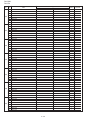
FO-6700U
FO-67DL
SW DATA
NO. NO.
SW15
SW16
SW17
SW18
SW19
SW20
1
2
3
4
5
6
7
8
1
2
3
4
5
6
7
8
1
2
3
4
5
6
7
8
1
2
3
4
5
6
7
8
1
2
3
4
5
6
7
8
1
2
3
4
5
6
7
8
Switch setting and function
ITEM
Reserved
Reserved
Reserved
Reserved
Cl Signal OFF detect enable time
1
Initial
setting
0
0
0
0
0
(ms)
No. 5
No. 6
No. 7
No. 8
200
0
0
0
0
300
0
0
0
1
No. 5
No. 6
No. 7
No. 8
OFF
0
0
0
0
STD RING1 RING2 RING3 RING4 RING5
0
1
0
1
0
1
0
0
1
1
0
0
0
0
0
0
1
1
1
0
0
0
0
0
Reserved
Reserved
Reserved
Reserved
Distinctive ringing
Reserved
Reserved
Reserved
Reserved
Reserved
Reserved
Reserved
Reserved
Reserved
Reserved
Reserved
Reserved
Reserved
Reserved
Reserved
Reserved
Reserved
Reserved
Reserved
Reserved
Reserved
Reserved
Reserved
Reserved
Reserved
Reserved
Reserved
Reserved
Reserved
Reserved
Reserved
Reserved
2 – 13
350
0
0
1
0
400
0
0
1
1
500
0
1
0
0
700
0
1
0
1
1200
0
1
1
0
0
1
0
1
0
0
0
0
0
0
0
0
0
0
0
0
0
0
0
1
1
0
0
0
1
1
0
0
1
0
0
0
1
0
0
0
0
0
0
0
0
0
0
0
Remarks
FO-6700U
FO-67DL
SW DATA
NO. NO.
1
2
3
SW21
SW22
SW23
SW24
SW25
SW26
4
5
6
7
8
1
2
3
4
5
6
7
8
1
2
3
4
5
6
7
8
1
2
3
4
5
6
7
8
1
2
3
4
5
6
7
8
1
2
3
4
5
6
7
8
Switch setting and function
ITEM
1
Reserved
Reserved
Reserved
Busy tone detection frequency
Initial
setting
0
0
0
0
No. 4
No. 5
No. 6
520~640Hz
0
0
0
Reserved
Reserved
Reserved
Reserved
Reserved
Reserved
Reserved
Reserved
Reserved
Reserved
Reserved
Reserved
Reserved
Reserved
Reserved
Reserved
Reserved
Reserved
Reserved
Reserved
Reserved
Reserved
Reserved
Reserved
Reserved
Reserved
Reserved
Reserved
Reserved
Reserved
Reserved
Reserved
Reserved
Reserved
Reserved
Reserved
Reserved
Reserved
Reserved
Reserved
Reserved
Reserved
2 – 14
300~600Hz 380~500Hz reserve
0
0
0
0
1
1
1
0
1
reserve
1
0
0
0
0
0
0
0
0
0
0
0
0
0
0
0
0
0
0
0
0
0
0
0
0
0
0
0
0
0
0
0
0
0
0
0
0
0
0
0
0
0
0
0
0
0
0
0
Remarks
FO-6700U
FO-67DL
SW DATA
NO. NO.
SW27
SW28
SW29
SW30
SW31
1
2
3
4
5
6
7
8
1
2
3
4
5
6
7
8
1
2
3
4
5
6
7
8
1
2
3
4
5
6
7
8
1
2
3
4
5
6
7
8
ITEM
Switch setting and function
1
Reserved
Reserved
Reserved
Reserved
Reserved
Reserved
Reserved
Reserved
Reserved
Reserved
Reserved
Reserved
Reserved
Reserved
Reserved
Reserved
Reserved
Reserved
Reserved
Reserved
Reserved
Reserved
Reserved
Reserved
Reserved
Reserved
Reserved
Reserved
Reserved
Reserved
Reserved
Reserved
Reserved
Reserved
Reserved
Reserved
Reserved
Reserved
Reserved
Reserved
0
Initial
setting
0
0
0
0
0
0
0
0
0
0
0
0
0
0
0
0
0
0
0
0
0
0
0
0
0
0
0
0
0
0
0
0
0
1
0
1
0
0
1
0
2 – 15
Remarks
FO-6700U
FO-67DL
SW DATA
NO. NO.
SW32
SW33
SW34
SW35
1
2
3
4
5
6
7
8
1
2
3
4
5
6
7
8
1
2
Dial mode
Reserved
Reserved
Reserved
Reserved
Reserved
Reserved
Reserved
Number of rings for auto-receive
(0: No ring receive)
3
4
5
6
7
8
1
2
3
4
5
6
7
8
1
2
3
4
Reserved
Reserved
Reserved
Reserved
Reserved
Reserved
Reserved
Reserved
Reserved
Reserved
Reserved
Reserved
Reserved
Reserved
JBIG (Joint Bi-level Image Group)
JBIG Option
MMR
MR
Modem speed
SW36
Switch setting and function
ITEM
1
PULSE
TONE
Binary input
8 4 2 1
No. =
1 2 3 4 (Data No.)
EX
0 0 0 1
eg. Number of rings for auto receive is set to 1 time
Reserved
Reserved
Reserved
Reserved
Reserved
Reserved
5
6
7
8
On
On
On
On
No. 5
No. 6
No. 7
No. 8
Reception speed fixed
1
2
3
0
Off
Off
Off
Off
V.33
V.17
V. 29
V. 27ter
14400 12000 14400 12000 9600 7200 9600 7200 4800 2400
0
0
1
1
1
1
0
0
0
0
1
1
0
0
0
0
0
0
0
0
0
1
0
1
0
1
0
1
1
0
0
0
0
0
1
1
1
1
0
0
NO
V. 17V. 29- V. 27ter14400bps 9600bps 4800bps
No. 1
0
1
0
1
No. 2
0
1
1
0
Once in NSF reception, twice
in DIS reception
Initial
setting
Remarks
0
1
0
0
1
1
0
0
0
0
0
1
0
0
0
0
0
0
OPTION
Set to 0~9
1
1
0
0
1
0
0
1
0
0
0
0
0
0
1
0
1
1
1
0
0
0
0
0
0
DIS receive acknowledge during
G3 transmission
Twice
4
Non-modulated carrier in V.29
On
Off
0
5
6
7
8
transmission mode
CNG send when manual TX
Protocol monitor
Line monitor
Reserved
On
On
On
Off
Off
Off
1
0
0
0
SW37
2 – 16
When 14400bps
MODEM used,
setting to
14400bps is
ignored.
Effective to
international
comm.
FO-6700U
FO-67DL
SW DATA
NO. NO.
Compromised equalizer
SW38
1
2
3
4
5
6
7
8
Switch setting and function
ITEM
H2 mode
Signal transmission level
1
No. 1
No. 2
0Km
0
0
1.8Km
7.2Km
0
1
1
1
No
Yes
Binary input
16 8 4 2 1
No. =
4 5 6 7 8 (Data No.)
EX
0 1 1 0 1
eg. Signal transmission level is set to -10dBm
No. 1
No. 2
75ms
0
0
CED tone signal interval
SW39
SW40
SW41
SW42
1
2
3
4
5
6
7
8
1
2
3
4
5
6
7
8
1
2
3
4
5
6
7
8
1
2
3
Equalizer freeze
Equalizer freeze conditions
CED detection time
Reserved
Reserved
Reserved
Reserved
Reserved
Reserved
Reserved
Reserved
Reserved
Reserved
Reserved
V.34 mode transmission speed
V.34 mode receiving speed
Reserved
V.34 mode function
V.34 control channel communication speed
EOL detection timer
4
5
Processing of DIS reception after DIS
transmission
SW43
6
7
8
1
2
3
4
5
6
7
8
The change to DB from DP by
DTMF output level (High)
Initial
setting
0
3.6Km
1
0
On
All
500ms
500ms
0
1
Off
7200bps
1000ms
750ms
1
0
1000ms
1
1
Sending speed = 2400 (bps) x N
Example :
2400 (bps) x 12 = 28800 (bps)
2400 (bps) is set for N=0. 33600 (bps) is set for N=15.
Receiving speed = 2400 (bps) x N
Example :
2400 (bps) x 12 = 28800 (bps)
2400 (bps) is set for N=0. 33600 (bps) is set for N=15.
On
2400bps
Off
1200bps
13sec
25sec
5sec
5sec
No. 4
0
0
1
1
No. 5
0
1
0
1
Retransmitting A line is Apply to T.30+α
command
cut
T.30
No. 6
0
0
1
1
No. 7
0
1
0
1
Yes
No
Binary input
16 8 4 2 1
No. =
1 2 3 4 5 (Data No.) n x 0.5dBm
EX
0 1 1 0 0
eg. Signal transmission level is set to -10dBm
Reserved
Reserved
Reserved
2 – 17
0
0
0
0
1
1
0
1
0
0
0
0
0
0
0
0
1
0
1
0
0
0
1
0
1
1
1
0
1
1
1
0
1
1
0
0
0
0
0
0
0
1
1
0
0
0
0
0
Remarks
Valid when
transmitting
FO-6700U
FO-67DL
SW DATA
NO. NO.
SW44
SW45
1
2
3
4
5
6
7
8
DTMF output level (Low)
Reserved
Reserved
Reserved
Frequency of CI signal
1
2
3
4
Cl signal off detect enable time
5
6
7
8
1
2
3
4
SW46
SW47
SW48
SW49
Switch setting and function
ITEM
1
0
Binary input
16 8 4 2 1
No. =
1 2 3 4 5 (Data No.) n x 0.5dBm
EX
1 0 0 0 0
eg. Signal transmission level is set to -10dBm
(Hz)
No. 1
No. 2
No. 3
No. 4
(ms)
No. 5
No. 6
No. 7
No. 8
Reserved
Reserved
Reserved
Reserved
Distinctive ringing
No. 5
No. 6
No. 7
No. 8
11.6~ 14.0~ 14.5~ 15.5~ 20.0~ 20.0~ 19.6~ 25.0~ 35.0~
76.9 76.9 76.9 76.9 58.8 66.6 76.9 58.8 76.9
0
0
0
0
0
0
0
0
1
0
0
0
0
1
1
1
1
0
0
0
1
1
0
0
1
1
0
0
1
0
1
0
1
0
1
0
200
300
350
400
500
700
1200
0
0
0
0
0
0
0
0
0
0
0
1
1
1
0
0
1
1
0
0
1
0
1
0
1
0
1
0
OFF
0
0
0
0
STD RING1 RING2 RING3 RING4 RING5
0
1
0
1
0
1
0
0
1
1
0
0
0
0
0
0
1
1
1
0
0
0
0
0
Initial
setting
1
0
0
0
0
0
0
0
0
0
0
0
0
1
0
1
0
0
0
0
5
6
7
8
1
2
3
4
5
6
7
8
1
2
3
4
5
6
7
8
1
2
3
4
5
6
Reserved
Reserved
Reserved
Reserved
Reserved
Reserved
Reserved
Reserved
Reserved
Reserved
Reserved
Reserved
Reserved
Reserved
Reserved
Reserved
Reserved
Reserved
Reserved
Reserved
Reserved
Reserved
0
0
0
0
0
0
0
0
0
0
0
1
1
0
0
0
1
1
0
0
1
0
0
0
1
0
7
8
Reserved
Reserved
0
0
2 – 18
Remarks
FO-6700U
FO-67DL
SW DATA
NO. NO.
Switch setting and function
ITEM
1
DTMF detection time
SW50
SW51
SW52
SW53
SW54
SW55
1
2
3
4
5
6
7
8
1
2
3
No. 1
No. 2
Reserved
Reserved
Reserved
Reserved
Reserved
Reserved
Reserved
Reserved
Reserved
Busy tone detection frequency
No. 4
No. 5
No. 6
520~640Hz
0
0
0
Initial
setting
0
100ms
1
0
120ms
1
1
300~600Hz 380~500Hz reserve
0
0
0
0
1
1
1
0
1
reserve
1
0
0
50ms
0
0
80ms
0
1
0
0
0
0
0
0
0
0
0
0
0
4
5
6
7
8
Reserved
Reserved
0
0
0
0
0
1
2
3
4
5
6
7
8
1
2
3
4
5
6
7
8
1
2
3
4
5
6
7
8
1
2
3
4
5
6
7
8
Reserved
Reserved
Reserved
Reserved
Reserved
Reserved
Reserved
Reserved
Reserved
Reserved
Reserved
Reserved
Reserved
Reserved
Reserved
Reserved
Reserved
Reserved
Reserved
Reserved
Reserved
Reserved
Reserved
Reserved
Reserved
Reserved
Reserved
Reserved
Reserved
Reserved
Reserved
Reserved
0
0
0
0
0
0
0
0
0
0
0
0
0
0
0
0
0
0
0
0
0
0
0
0
0
0
0
0
0
0
0
0
2 – 19
Remarks
FO-6700U
FO-67DL
SW DATA
NO. NO.
SW56
SW57
SW58
SW59
SW60
Switch setting and function
ITEM
1
Initial
setting
0
1
2
3
4
5
6
7
8
1
2
3
4
5
6
7
8
1
2
Reserved
Reserved
Reserved
Reserved
Reserved
Reserved
Reserved
Reserved
Reserved
Reserved
Reserved
Reserved
Reserved
Reserved
Reserved
Reserved
Reserved
Reserved
0
0
0
0
0
0
0
0
0
0
0
0
0
0
0
0
0
0
3
4
5
6
7
8
1
2
3
4
5
6
7
8
1
2
3
4
5
6
7
8
1
2
3
4
Reserved
Reserved
Reserved
Reserved
Reserved
Reserved
Reserved
Reserved
Reserved
Reserved
Reserved
Reserved
Reserved
Reserved
Reserved
Reserved
Reserved
Reserved
Reserved
Reserved
Reserved
Reserved
F.A.S.T. (RMS) mode
F.A.S.T. (RMS) line
Verification stamp
Day light saving
Key buzzer volume
0
0
0
0
0
0
0
0
0
0
0
0
0
0
0
0
0
0
0
0
0
0
0
0
0
1
SW61
5
6
7
8
On
Line-2
Yes
No
No. 5
No. 6
Reserved
Reserved
2 – 20
Off
0
0
Off
Line-1
No
Yes
High
0
1
Low
1
0
Low
1
1
1
0
0
0
Remarks
FO-6700U
FO-67DL
SW DATA
NO. NO.
Switch setting and function
ITEM
1
No. 1
No. 2
High
0
0
High
0
1
0
Middle
1
0
No. 5
No. 6
Off
0
0
High
0
1
Middle
1
0
Speaker volume
SW62
SW63
SW64
1
2
3
4
5
6
7
8
1
2
3
4
5
6
7
8
1
2
3
4
5
6
7
8
Reserved
Reserved
Ringer volume
Reserved
Reserved
Reserved
PC I/F mode
Reserved
Reserved
Reserved
Reserved
Reserved
Reserved
Header registration
Reserved
Continuous serial polling
Time interval for continuous serial polling
Reserved
Reserved
Quick on-line function
Cassette selection
1
2
The 1st priority cassette
SW65
3
4
5
The 2nd priority cassette
6
7
8
The 3rd priority cassette
SW66
1
2
3
4
5
6
7
8
Reserved
Reserved
Reserved
Reserved
Print hold function
On
Off
On
Off
On
Initial
setting
Low
1
1
Low
1
1
No. 4
No. 5
0 min.
0
0
Off
30 min.
0
1
No. 1
No. 2
None
No. 3
0
No. 4
0
No. 5
0
None
No. 6
0
No. 7
0
No. 8
0
None
No. 1
0
No. 2
0
No. 3
0
Manual
0
0
Tray
0
0
1
Tray
0
0
1
Tray
0
0
1
No
Auto-1
Auto-2
Auto-1
0
1
1
1
0
1
1st Cass. 2nd Cass.
Tray
0
0
Other
1
1
Combination
0
1
1st Cass. 2nd Cass.
Tray
0
0
Other
1
1
Combination
0
1
1st Cass. 2nd Cass.
Tray
0
0
Other
1
1
Combination
0
1
Yes
On
Off
2 – 21
60 min.
1
0
120 min.
1
1
Remarks
1
1
1
0
1
1
0
0
0
1
0
0
0
0
0
0
0
0
0
0
0
0
0
1
OPTION
When SW64-No.3
is on, option setting
can be set up
OPTION
0
1
0
1
0
0
1
1
0
0
1
0
0
0
0
0
OPTION
It is effective
only when
No.31-1/2 are
set up of manual
OPTION
It is effective
only when
No.31-1/2 are
set up of manual
OPTION
It is effective
only when
No.31-1/2 are
set up of manual
FO-6700U
FO-67DL
SW DATA
NO. NO.
Heater mode
1
2
Density adjustment of print bias
SW67
SW68
SW69
SW70
SW71
SW72
3
4
5
6
7
8
1
2
3
4
5
6
7
8
1
2
3
4
5
6
7
8
1
2
3
4
5
6
7
8
1
2
3
4
5
6
7
8
1
2
3
4
5
6
7
8
Switch setting and function
ITEM
Reserved
Reserved
Reserved
The default resolution for copying
Reserved
Reserved
Line for relay TX
1
0
Always on
Always off
Off timer
No.1
0
0
1
No.2
0
1
0
Binary input
4 2 1
No. =
3 4 5 (Data No.) 1: faint 6: deep
EX
1 0 0
eg. Bias is set to level 4.
Super Fine
No. 4
No. 5
Fine
AUTO
0
0
Line-1
0
1
Line-2 Not use(AUTO)
1
1
0
1
Reserved
Reserved
Reserved
Reserved
Reserved
Reserved
Reserved
Reserved
Reserved
Reserved
Reserved
Reserved
Reserved
Reserved
Reserved
Reserved
Reserved
Reserved
Reserved
Delay time after PC printing
(n second)
Initial
setting
OPTION
0
1
1
0
0
0
0
0
0
0
0
0
0
0
0
0
0
1
1
1
0
1
1
0
0
0
1
0
0
0
0
1
Binary input
No. =
EX
Reserved
Reserved
Reserved
Reserved
Reserved
Reserved
Reserved
Reserved
2 – 22
128 64 32 16 8
1 2 3 4 5
0 0 0 0 0
4
6
1
2
7
1
1
8 (Data No.)
0 (= 6 sec)
Remarks
0
0
0
0
0
1
1
0
0
0
0
0
0
0
0
0
set to 1~7.
set to 0, is
equal to 4
(100)
OPTION
FO-6700U
FO-67DL
SW DATA
NO. NO.
SW73
SW74
SW75
1
2
3
4
5
6
7
8
1
2
3
4
5
6
7
8
1
2
3
4
5
6
7
8
1
2
SW76
SW77
SW78
3
4
5
6
7
8
1
2
3
4
5
6
7
8
1
2
3
4
5
6
7
8
ITEM
Switch setting and function
1
Reserved
Reserved
Reserved
Reserved
Reserved
Data reduction
(Except notation: Setting prohibition)
0
Initial
setting
Remarks
0
0
0
0
0
AUTO
100%
No. 6
0
1
Set up to 100% except the
No. 7
0
0
notation
No. 8
0
0
Automatic printing of activity report
Yes (When momory full)
No (First data is cleared when memory full)
Print out of total time and total number of pages on activity report Off
On
Reserved
Department function
On
Off
Department ID digit
Binary inout
8 4 2 1
No. =
5 6 7 8 (Data No.)
EX
0 1 0 0
eg. Department ID is set to 4 digits
Picture quality priority mode
Fine
Standard
Cut-off mode (when copy mode)
Continue
Cut-off
Scanning ratio in momory input
1:1
Reduce
Overseas communication mode selection function Yes
No
Reserved
Reduce ratio when copy mode
AUTO
100%
(Except notation: Setting prohibition)
No. 6
0
1
Set up to 100% except the
No. 7
0
0
notation
No. 8
0
0
Reserved
Reserved
Normal
Faint
Deep
Deep (when Dark mode)
Density adjustment (when Fine/STD mode)
No. 3
0
0
1
1
No. 4
0
1
0
1
Density adjustment (when Half-tone mode)
Normal
Faint
Deep
Deep (when Dark mode)
No. 5
0
0
1
1
No. 6
0
1
0
1
MTF correction in half-tone mode
On
Off
MTF intensity in half-tone mode
Strong
Weak
Cassette define LTR/A4: Tray
A4
LTR
Cassette define LTR/A4: Upper
A4
LTR
Cassette define LTR/A4: Lower
A4
LTR
Reserved
Reserved
Dial selection
Line-1 TX/RX TX/RX TX/RX RX
RX
TX
TX
Line-2 TX/RX RX
TX TX/RX TX TX/RX RX
No. 6
0
0
0
0
1
1
1
No. 8
0
0
1
1
0
0
1
No. 8
0
1
0
1
0
1
0
Reserved
Reserved
Reserved
Reserved
Reserved
Reserved
Reserved
Reserved
2 – 23
0
0
0
0
0
0
0
0
1
0
0
0
0
0
0
0
1
0
0
0
0
0
0
0
0
1
0
0
0
0
0
0
0
0
0
1
0
0
0
0
0
0
1
OPTION
OPTION
set to 3~9
OPTION
OPTION
Memory scanning
FO-6700U
FO-67DL
SW DATA
NO. NO.
SW79
SW80
SW81
SW82
SW83
SW84
SW85
1
2
3
4
5
6
7
8
1
2
3
4
5
6
7
8
1
2
3
4
5
6
7
8
1
2
3
4
5
6
7
8
1
2
3
4
5
6
7
8
1
2
3
4
5
6
7
8
1
2
3
4
5
6
7
8
Switch setting and function
ITEM
Secure billing code
Pause with SHIFT key
Reserved
Z key pause time
(250ms unit)
Separate feature
Reserved
Reserved
Use personal book name as multi TTI
Addition of header (Sender information)
DTMF sending by the panel test
Power save mode
Ring control for line-2
Reserved
Reserved
Reserved
Reserved
Reserved
Reserved
Reserved
Reserved
Reserved
Reserved
Reserved
Reserved
Reserved
Reserved
Reserved
Reserved
Reserved
Reserved
Reserved
Reserved
Reserved
Reserved
Reserved
Reserved
Reserved
Reserved
Reserved
Reserved
Reserved
Reserved
Reserved
Reserved
Reserved
Reserved
Reserved
Reserved
Reserved
Reserved
Reserved
Reserved
1
Yes
Yes
0
No
No
Binary input
16 8 4 2 1
No. =
4 5 6 7 8 (Data No.)
EX
0 0 0 0 0
eg. Pause time 250ms
Time=(n+1) x 250ms
On
Off
Yes
On
On
Real time
On
2 – 24
No
Off
Off
Timer
Off
Initial
setting
0
0
0
0
0
0
0
0
0
0
0
0
1
0
1
0
1
0
1
1
1
1
1
1
0
1
0
1
0
0
0
0
0
0
0
0
0
1
0
1
0
0
0
0
1
0
0
1
0
0
0
0
0
0
0
0
Remarks
FO-6700U
FO-67DL
SW DATA
NO. NO.
SW86
SW87
SW88
SW89
SW90
SW91
SW92
Switch setting and function
ITEM
1
0
Initial
setting
1
2
3
4
5
6
7
8
1
2
3
4
5
6
7
8
1
2
Reserved
Reserved
Reserved
Reserved
Reserved
Reserved
Reserved
Reserved
Reserved
Reserved
Reserved
Reserved
Reserved
Reserved
Reserved
Reserved
Reserved
Reserved
0
0
0
1
0
1
1
1
0
0
0
0
0
0
0
0
0
0
3
4
5
6
7
8
1
2
3
4
5
6
7
8
1
2
3
4
5
6
7
8
1
2
3
4
5
6
7
8
1
2
3
4
5
6
7
8
Reserved
Reserved
Reserved
Reserved
Reserved
Reserved
Reserved
Reserved
Reserved
Reserved
Reserved
Reserved
Reserved
Reserved
Reserved
Reserved
Reserved
Reserved
Reserved
Reserved
Reserved
Reserved
Reserved
Reserved
Reserved
Reserved
Reserved
Reserved
Reserved
Reserved
Reserved
Reserved
Waiting time after dialing
Show receiver’s name
Reserved
Reserved
Reserved
Reserved
0
0
0
0
0
0
0
0
0
0
0
0
0
0
0
1
0
0
0
1
0
1
0
0
0
0
0
0
0
0
0
1
0
1
0
0
0
0
90sec
Yes (Show)
2 – 25
The specification of each country is followed
No (Hide)
Remarks
FO-6700U
FO-67DL
SW DATA
NO. NO.
SW93
SW94
SW95
SW96
SW97
SW98
SW99
1
2
3
4
5
6
7
8
1
2
3
4
5
6
7
8
1
2
3
4
5
6
7
8
1
2
3
4
5
6
7
8
1
2
3
4
5
6
7
8
1
2
3
4
5
6
7
8
1
2
3
4
5
6
7
8
ITEM
Switch setting and function
1
Reserved
Reserved
Reserved
Reserved
Reserved
Reserved
Reserved
Reserved
Reserved
Reserved
Reserved
Reserved
Reserved
Reserved
Reserved
Reserved
Reserved
Reserved
Reserved
Reserved
Reserved
Reserved
Reserved
Reserved
Reserved
Reserved
Reserved
Reserved
Reserved
Reserved
Reserved
Reserved
Reserved
Reserved
Reserved
Reserved
Reserved
Reserved
Reserved
Reserved
Reserved
Reserved
Reserved
Reserved
Reserved
Reserved
Reserved
Reserved
Reserved
Reserved
Reserved
Reserved
Reserved
Reserved
Reserved
Reserved
0
Initial
setting
0
0
0
0
0
0
0
0
0
0
0
0
0
0
0
0
0
0
0
0
1
1
0
1
0
0
0
0
0
0
0
0
0
0
0
0
0
0
0
0
0
0
0
0
0
0
0
0
0
0
0
0
0
0
1
1
2 – 26
Remarks
FO-6700U
FO-67DL
SW4 No. 1 ~ No. 3 Communication results printout
• Soft switch function description
It is possible to obtain communication results after each transaction.
Normally, the switch is set (No. 1: 0, No. 2: 0, No. 3: 1) so that the communication result is produced only a communication error is en-countered. If No. 1 was set to 1, No. 2 was set to 1 and No. 3 was set to 0, the
communication result will be produced every time a communication is
done, even if the communication was successful.
SW1 No. 1 ~ No. 4 Recall interval
Choice is made for a recall interval for speed and rapid dial numbers.
Use a binary number to program this. If set to 0 accidentally, 1 will be
assumed.
SW1 No. 5 ~ No. 8 Recall times
If No. 1 was set to 0, No. 2 to 1 and No. 3 to 0, the communication result
will be produced every transmission.
Choice is made as to how many recall times should be made. Use a
binary number to program this.
Setting No. 1 to 1 No. 2 to 0 and No. 3 to 0 will disable this function. No
transaction report will be printed.
SW2 No. 1 Dial mode
Switch the type according to the telephone circuit connected to the facsimile.
If No. 1 was set to 0, No. 2 to 0 and No. 3 to 0, the communication result
is produced only after a timer and memory transmission or when a communication error is encountered.
0: PULSE DIAL
1: TONE DIAL
SW4 No. 4 Image addition function to the communication result
table (for memory transmission only)
SW2 No. 2 Receive mode
Used to set addition of sending image to the communication result table.
Auto/manual receiving mode is set.
SW4 No. 5 Reserved
SW2 No. 3 ECM mode
Set to "0".
Used to determine ECM mode function.
SW4 No. 6 TEL billing code function
SW2 No. 4 Reserved
When set to "1", the TEL billing code function is enabled.
Set to "0".
SW4 No. 7 Billing code position
SW2 No. 5 Polling security
When set to "1", the billing code is delivered before dialing the remote
number. When set to "0", the billing code is delivered after dialing.
This switch is employed to enable or disable the polling operation using
the ID code verification function, in order to prevent unauthorized polling
operation.
SW4 No. 8 Multi-TTI feature
SW2 No. 6 Auto cover sheet
When this switch is set to "1", Multi TTI function is enabled.
When "1" (=YES) is selected, the cover sheet is automatically sent after
transmission of the original to notify the receiver of the number of original sheets transmitted.
SW5 No. 1 Time display format
When this switch is set to "0", time is displayed in 12-hour system.
When set to "1", 24-hour system.
SW2 No. 7 JUNK-FAX function in manual reception
SW5 No. 2 Date display format
It is set whether JUNK-FAX is functioned in the manual receiving mode
or not.
Used to select date display/print formats.
0: DAY-Month-Year
SW2 No. 8 JUNK-FAX function
1: Month-DAY-Year
This function is used to receive data from a specific remote machine
(station registered in entry mode). It is the function that refused a reception in the case that TSI of remote machine matched with fax number of
the station registered.
SW5 No. 3 Header print
When it is set at 0, sender’s name, sending page number and so on are
automatically printed in the recording paper on the receiving side during
transmission. Thus, the sender can be known on the receiving side.
0: No
1: Yes
0: Applied.
1: Not applied.
SW3 No. 1 ~ No. 4 Number of rings for auto-receive
(0: No ring receive)
SW5 No. 4 Footer print
When the machine is set in the auto receive mode, the number of rings
before answering can be selected. It may be set from one to nine rings
using a binary number. If the soft switch was set to 1, a direct connection
is made to the facsimile. If it was set to 0 accidentally, receive ring is set
to 1. If it was above 9, receive rings are set to 9.
When set to "1", the date of reception, the sender machine No., and the
page No. are automatically recorded at the end of reception.
SW5 No. 5 Relay data output
0: Output ON
SW3 No. 5 ~ No. 8 Switch to auto-receive from manual receive
(0: No switch)
1: Output OFF
SW5 No. 6 Substitute reception
This setting allows machine to switch from manual to Auto Receive mode.
Setting this number to 0 forces machine to stay in Manual receive mode.
Entering the binary number 0 forces the machine to remain in the manual
answer mode. If a number between 1 and 9 is entered, the machine will
go into the answer mode after the given number of rings. However, it can
be used as an ordinary telephone if the handset is taken off the hook
before this programmed number is finished. If entry of a number above 9
by accident, it will be set to 9. In this case, it must be corrected to the
proper number.
Selection of substitute reception in the case of recording paper ex-hausted
or paper jam. If set to "NO", auto receive is disabled even when the
receive memory is ready to receive.
Substitute reception is not performed even during receive operation.
SW5 No. 7 Substitute reception conditions
Selection of substitute reception according to existence of TEL number
from transmitting side. Initial setting allows substitute reception without
CSI. If set to "no", the receiver cannot receive any documents
SW5 No. 8 CSI transmission
CSI signal contains the sender’s phone number registered in the machine. If this switch is set to "1", no sender’s name will be printed at the
receiving side.
2 – 27
FO-6700U
FO-67DL
SW6 No. 1 JBIG (Joint Bi-level Image Group)
SW9 No. 1, No. 2 CED tone signal interval
An image compression encoding method recommended by ITU-T.
It realizes 2-second transmission when the power is turned on.
An optional function for JBIG.
For international communication, the 2100Hz CED tone may act as an
echo suppresser switch, causing a communication problem. Though this
soft switch is normally set to "0", it should be set to "1" so as to change
the time between CED tone and DIS signal from 75ms to 500ms to eliminate the communication problem caused by echo.
SW6 No. 3 MMR
SW9 No. 3 Equalizer freeze
MMR (Modified MR) selects presence of the compression function.
MR (Modified READ) selects presence of the compression function.
This switch is used to perform reception operation by fixing the equalizer control of modem for the line which is always in an unfavorable state
and picture cannot be received. Usually, the control is executed according to the state of line where the equalizer setting is changed always.
SW6 No. 5 ~ No. 8 Modem speed
SW9 No. 4 Equalizer freeze conditions
Used to determine the initial modem speed. The default is
14400BPS(V.17). It may be necessary to program it to a slower speed
when frequent line fallback is encountered, in order to save the time
required for the fallback procedure.
Setting which specifies SW9 No.3 control only in condition of 7200bps
modem speed.
SW6 No. 2 JBIG option
SW6 No. 4 MR
SW9 No. 5 CED detection time
The detection time of the CED signal from the called side in the auto
calling mode is set.
SW7 No. 1, No. 2 Reception speed fixed
The transferable speed of modem in the receiving mode is set.
SW9 No. 6, No. 7 Alarm buzzer
SW7 No. 3 DIS receive acknowledge during G3 transmission
The length of the buzzer for normal end of operation is set.
Used to make a choice of whether reception of NSF (DIS) is acknowledged after receiving two NSFs (DISs) or receiving one NSF (two DISs).
SW9 No. 8 Action when RTN received
It may be useful for overseas communication to avoid an echo suppression problem, if set to 1.
The operation is set when the RTN signal is received in the G3 transmission mode.
SW7 No. 4 Non-modulated carrier in V.29 transmission mode
SW10 No. 1 ~ No. 4 Memory retransmission times
Though transmission of a non-modulated carrier is not required for transmission by the V29 modem according to the CCITT Recommendation, it
may be permitted to send a non-modulated carrier before the image
signal to avoid an echo suppression problem. It may be useful for overseas communication to avoid an echo sup-pression problem, if set to 1.
The number of memory retransmissions is set.
SW7 No. 5 CNG send when manual TX
CNG signal sending ON/OFF in case of manual transmission is set.
Used to determine the initial modem speed when communication method
is V.34 transmission mode.
SW7 No. 6 Protocol monitor
SW11 No. 5 ~ No. 8 V.34 mode receiving speed
Normally set to "0". If set to "1", communication can be checked, in case
of troubles, without using a G3 tester or other tools.
Used to determine the initial modem speed when communication method
is V.34 reception mode.
When communication FSK data transmission or reception is made, the
data is taken into buffer. When communication is finished, the data
analyzed and printed out. When data is received with the line monitor
(SW7-No. 7) set to "1" the reception level is also printed out.
SW12 No. 1 V.34 mode function in case of manual communication
SW10 No. 5 ~ No. 8 Memory retransmission interval
The interval between memory retransmissions is set.
SW11 No. 1 ~ No. 4 V.34 mode transmission speed
Used to select whether the V.34 mode is made valid when automatically
transmitting/receiving.
SW12 No. 2 V.34 mode function
SW7 No. 7 Line monitor
Used to select the V.34 mode for communication when set to “1”, communication method is V.34 mode..
Normally set to "0". If set to "1", the transmission speed and the reception level are displayed on the LCD. Used for line tests.
SW12 No. 3 V.34 control channel communication speed
SW7 No. 8 Max. length for TX/RX/Copy
Used to select the control channel communication speed for V.34 mode.
Used to set the maximum page length.
SW12 No. 4, No. 5 EOL detection timer
To avoid possible paper jam, the page length is normally limited to 432
mm for copy or transmit, and 1.5 meters for receive.
Used to make a choice of whether to use the 25-second or 13-second
timer for detection of End of line This is effective to override communication failures with some facsimile models that have longer End of line
detection.
It is possible to set it to "No limit" to transmit/receive a long document,
such as a computer print form, etc. (In this case, the receiver/transmitter must also be set to no limit.)
SW12 No. 6, No. 7 Processing of DIS reception after DIS transmission
SW8 No. 1, No. 2 Compromised equalizer
The specific line equalizer is inserted.
When receiving , operation in case of DIS reception after DIS transmission is selected. Retransmitting command: To retransmit DIS in disregard of DIS reception.
Breaking circuit: To break circuit instantly. (Abnormal finish)
T. 30: To operate in accordance with T.30.
T. 30+α: To operate in accordance with T.30+α. (To operate differently
according to cases.)
No. 1 No. 2
0
0
The line equalizer built in the modem is turned off.
0
1
Line equalizer corresponding to 1.8 km
1
0
Line equalizer corresponding to 3.6 km
0
1
Line equalizer corresponding to 7.2 km
SW8 No. 3 H2 mode
SW12 No. 8 The change to DB from DP by
Used to determine H2 mode (15sec transmission mode). When set to
OFF, H2 mode is inhibited even though the transmitting machine has
H2 mode.
When setting to 1, the mode is changed by pressing the
pulse dial mode to the tone dial mode.
key from the
SW13 No. 1 ~ No. 5 DTMF output level (High)
SW8 No. 4 ~ No. 8 Signal transmission level
To set the level to output high group DTMF signals. –15 to 0 dBm (0.5
dBm unit)
Used to control the signal transmission level in the range of –0dB to
–31dB.
2 – 28
FO-6700U
FO-67DL
SW13 No. 6 ~ No. 8 Reserved
SW18 No. 2 ~ No. 4 Reserved
Set to "0".
Set to "0".
SW14 No. 1 ~ No. 5 DTMF output level (Low)
SW18 No. 5 , No. 6 Reserved
To set the level to output low group DTMF signals. –15 to 0 dBm (0.5
dBm unit)
Set to "1".
SW14 No. 6 ~ No. 8 Reserved
Set to "0".
SW18 No. 7 , No. 8 Reserved
Set to "0".
SW19 No. 1 Reserved
SW15 No. 1 ~ No. 4 Reserved
Set to "1".
Set to "0".
SW19 No. 2 ~ No. 4 Reserved
SW15 No. 5 ~ No. 8 Cl signal OFF detect enable time
Set to "0".
Used to set the continuous detection time during OFF period of Cl signal.
SW19 No. 5 Reserved
Set to "1".
SW16 No. 1 ~ No. 4 Reserved
SW19 No. 6 ~ No. 8 Reserved
Set to "0".
Set to "0".
SW16 No. 5 ~ No. 8 Distinctive ringing
SW20 No. 1 ~ No. 8 Reserved
When the ringing setting is turned off, all of the CI signal are received.
When any of the standard, and ring patterns 1 through 3 is selected for
the ringing setting, only the selected CI signal is received.
Set to "0".
SW21 No. 1 ~ No. 3 Reserved
CI signal patterns
The CI signal patterns consists of the standard pattern, and ring patterns 1 through 7. The standard pattern is the conventional one.
Set to "0".
SW21 No. 4 ~ No. 6 Busy tone detection frequency
To select frequency range of signals to be detected as Busy Tone.
2S
SW21 No. 7, No. 8 Reserved
4S
Set to "0".
2S
SW22 No. 1 ~ No. 8 Reserved
2S
Set to "0".
1.5S
SW23 No. 1 ~ No. 8 Reserved
STANDARD
3S
Set to "0".
1S
SW24 No. 1 ~ No. 8 Reserved
4S
Set to "0".
0.5S
1.5S
SW25 No. 1 ~ No. 8 Reserved
0.5S
RING
PATTERN 1
for USA
4S
SW26 No. 1 ~ No. 8 Reserved
0.4S
RING
PATTERN 2
for USA
SW27 No. 1 ~ No. 8 Reserved
0.2S
0.4S 0.4S 0.8S
SW28 No. 1 ~ No. 8 Reserved
Set to "0".
SW30 No. 1 ~ No. 8 Reserved
1S
1S
0.5S
Set to "0".
3.5S
1S
0.5S
0.5S
RING
PATTERN 3
for CANADA
SW29 No. 1 ~ No. 8 Reserved
3S
0.5S
RING
PATTERN 2
for CANADA
Set to "0".
4S
1S
1S
1S
RING
PATTERN 1
for CANADA
Set to "0".
4S
0.2S 0.2S
RING
PATTERN 4
for USA
Set to "0".
4S
0.3S
0.3S 1S
0.2S
RING
PATTERN 3
for USA
Set to "0".
0.8S
0.8S
SW31 No. 1 Reserved
0.5S
0.5S
0.5S
Set to "0".
3S
SW31 No. 2 Reserved
1S
Set to "1".
0.5S
0.5S
3S
SW31 No. 3 Reserved
Set to "0".
SW17 No. 1 ~ No. 7 Reserved
SW31 No. 4 Reserved
Set to "0".
Set to "1".
SW17 No. 8 Reserved
SW31 No. 5, No. 6 Reserved
Set to "1".
Set to "0".
SW18 No. 1 Reserved
SW31 No. 7 Reserved
Set to "1".
Set to "1".
2 – 29
FO-6700U
FO-67DL
SW31 No. 8 Reserved
SW37 No. 1, No. 2 Reception speed fixed
Set to "0".
The transferable speed of modem in the receiving mode is set.
SW32 No. 1 Dial mode
SW37 No. 3 DIS receive acknowledge during G3 transmission
Switch the type according to the telephone circuit connected to the facsimile.
Used to make a choice of whether reception of NSF (DIS) is acknowledged after receiving two NSFs (DISs) or receiving one NSF (two DISs).
0: PULSE DIAL
It may be useful for overseas communication to avoid an echo suppression problem, if set to 1.
1: TONE DIAL
SW37 No. 4 Non-modulated carrier in V.29 transmission mode
SW32 No. 2 Reserved
Though transmission of a non-modulated carrier is not required for transmission by the V29 modem according to the CCITT Recommendation, it
may be permitted to send a non-modulated carrier before the image
signal to avoid an echo suppression problem.
Set to "1".
SW32 No. 3, No. 4 Reserved
Set to "0".
It may be useful for overseas communication to avoid an echo suppression problem, if set to 1.
SW32 No. 5, No. 6 Reserved
Set to "1".
SW37 No. 5 CNG send when manual TX
SW32 No. 7, No. 8 Reserved
CNG signal sending ON/OFF in case of manual transmission is set.
Set to "0".
SW37 No. 6 Protocol monitor
SW33 No. 1 ~ No. 4 Number of rings for auto-receive
(0: No ring receive)
Normally set to "0". If set to "1", communication can be checked, in case
of troubles, without using a G3 tester or other tools.
When the machine is set in the auto receive mode, the number of rings
before answering can be selected. It may be set from one to nine rings
using a binary number. If the soft switch was set to 1, a direct connection
is made to the facsimile. If it was set to 0 accidentally, receive ring is set
to 1. If it was above 9, receive rings are set to 9.
When communication FSK data transmission or reception is made, the
data is taken into buffer. When communication is finished, the data
analyzed and printed out. When data is received with the line monitor
(SW7-No. 7) set to "1" the reception level is also printed out.
SW37 No. 7 Line monitor
SW33 No. 5 ~ No. 8 Reserved
Set to "0".
Normally set to "0". If set to "1", the transmission speed and the reception level are displayed on the LCD. Used for line tests.
SW34 No. 1, No. 2 Reserved
SW37 No. 8 Reserved
Set to "0".
Set to "0".
SW34 No. 3, No. 4 Reserved
SW38 No. 1, No. 2 Compromised equalizer
Set to "1".
The specific line equalizer is inserted.
SW34 No. 5, No. 6 Reserved
No. 1 No. 2
Set to "0".
0
0
The line equalizer built in the modem is turned off.
SW34 No. 7 Reserved
0
1
Line equalizer corresponding to 1.8 km
Set to "1".
1
0
Line equalizer corresponding to 3.6 km
SW34 No. 8 Reserved
0
1
Line equalizer corresponding to 7.2 km
Set to "0".
SW38 No. 3 H2 mode
SW35 No. 1 Reserved
Used to determine H2 mode (15sec transmission mode). When set to
OFF, H2 mode is inhibited even though the transmitting machine has H2
mode.
Set to "0".
SW35 No. 2 Reserved
SW38 No. 4 ~ No. 8 Signal transmission level
Set to "1".
Used to control the signal transmission level in the range of –0dB to
–31dB.
SW35 No. 3 ~ No. 8 Reserved
Set to "0".
SW39 No. 1, No. 2 CED tone signal interval
SW36 No. 1 JBIG (Joint Bi-level Image Group)
For international communication, the 2100Hz CED tone may act as an
echo suppresser switch, causing a communication problem. Though this
soft switch is normally set to "0", it should be set to "1" so as to change
the time between CED tone and DIS signal from 75ms to 500ms to
eliminate the communication problem caused by echo.
An image compression encoding method recommended by ITU-T.
It realizes 2-second transmission when the power is turned on.
SW36 No. 2 JBIG option
An optional function for JBIG.
SW39 No. 3 Equalizer freeze
SW36 No. 3 MMR
MR (Modified READ) selects presence of the compression function.
This switch is used to perform reception operation by fixing the equalizer control of modem for the line which is always in an unfavorable
state and picture cannot be received. Usually, the control is executed
according to the state of line where the equalizer setting is changed
always.
SW36 No. 5 ~ No. 8 Modem speed
SW39 No. 4 Equalizer freeze conditions
Used to determine the initial modem speed. The default is
14400BPS(V.17). It may be necessary to program it to a slower speed
when frequent line fallback is encountered, in order to save the time
required for the fallback procedure.
Setting which specifies SW9 No.3 control only in condition of 7200bps
modem speed.
MMR (Modified MR) selects presence of the compression function.
SW36 No. 4 MR
SW39 No. 5 CED detection time
The detection time of the CED signal from the called side in the auto
calling mode is set.
2 – 30
FO-6700U
FO-67DL
SW39 No. 6 ~ No. 8 Reserved
SW45 No. 5 ~ No. 8 CI signal off detect enable time
Set to "0".
Used to set the continuous detection time during OFF period of CI signal. Normally set to 700ms, where the short ring (500ms: OFF period)
cannot be detected. Therefore, selection of 350ms is allowed.
SW40 No. 1 Reserved
Set to "1".
SW46 No. 1 ~ No. 4 Reserved
SW40 No. 2 Reserved
Set to "0".
Set to "0".
SW46 No. 5 ~ No. 8 Distinctive ringing
SW40 No. 3 Reserved
When the ringing setting is turned off, all of the CI signal are received.
When any of the standard, and ring patterns 1 through 3 is selected for
the ringing setting, only the selected CI signal is received.
Set to "1".
SW40 No. 4 ~ No. 6 Reserved
CI signal patterns
The CI signal patterns consists of the standard pattern, and ring patterns 1 through 7. The standard pattern is the conventional one.
Set to "0".
SW40 No. 7 Reserved
Set to "1".
2S
SW40 No. 8 Reserved
4S
Set to "0".
2S
SW41 No. 1 ~ No. 4 V.34 mode transmission speed
2S
Used to determine the initial modem speed when communication method
is V.34 transmission mode.
1.5S
STANDARD
3S
SW41 No. 5 ~ No. 8 V.34 mode receiving speed
1S
Used to determine the initial modem speed when communication method
is V.34 reception mode.
4S
0.5S
1.5S
SW42 No. 1 Reserved
Set to "1".
0.5S
SW42 No. 2 V.34 mode function
RING
PATTERN 1
for USA
Used to select the V.34 mode for communication when set to “1”, communication method is V.34 mode..
0.4S
RING
PATTERN 2
for USA
SW42 No. 3 V.34 control channel communication speed
SW42 No. 4, No. 5 EOL detection timer
RING
PATTERN 3
for USA
Used to make a choice of whether to use the 25-second or 13-second
timer for detection of End of line This is effective to override communication failures with some facsimile models that have longer End of line
detection.
RING
PATTERN 4
for USA
4S
0.3S
0.3S 1S
0.2S
0.2S
Used to select the control channel communication speed for V.34 mode.
4S
0.4S 0.4S 0.8S
0.2S 0.2S
4S
1S
1S
3S
1S
RING
PATTERN 1
for CANADA
SW42 No. 6, No. 7 Processing of DIS reception after DIS transmission
1S
1S
0.5S
When receiving , operation in case of DIS reception after DIS transmission is selected. Retransmitting command: To retransmit DIS in disregard of DIS reception.
Breaking circuit: To break circuit instantly. (Abnormal finish)
T. 30: To operate in accordance with T.30.
T. 30+α: To operate in accordance with T.30+α. (To operate differently
according to cases.)
RING
PATTERN 2
for CANADA
0.5S
0.5S
0.5S
SW47 No. 1 ~ No. 7 Reserved
Set to "0".
key from the
SW47 No. 8 Reserved
Set to "1".
To set the level to output high group DTMF signals. –15 to 0 dBm (0.5
dBm unit)
SW48 No. 1 Reserved
SW43 No. 6 ~ No. 8 Reserved
SW48 No. 2 ~ No. 4 Reserved
Set to "0".
Set to "0".
SW44 No. 1 ~ No. 5 DTMF output level (Low)
SW48 No. 5, No. 6 Reserved
To set the level to output low group DTMF signals. –15 to 0 dBm (0.5
dBm unit)
Set to "1".
SW44 No. 6 ~ No. 8 Reserved
Set to "0".
Set to "1".
SW48 No. 7, No. 8 Reserved
Set to "0".
SW49 No. 1 Reserved
SW45 No. 1 ~ No. 4 Frequency of CI signal
Set to "1".
Used to set the detection frequency of CI signal.
SW49 No. 2 ~ No. 4 Reserved
Set to "0".
2 – 31
0.5S
0.5S
0.5S
SW43 No. 1 ~ No. 5 DTMF output level (High)
3.5S
1S
0.5S
0.5S
RING
PATTERN 3
for CANADA
SW42 No. 8 The change to DB from DP by
When setting to 1, the mode is changed by pressing the
pulse dial mode to the tone dial mode.
4S
0.8S
0.8S
3S
1S
3S
FO-6700U
FO-67DL
SW49 No. 5 Reserved
SW62 No. 3 Reserved
Set to "1".
Set to "1".
SW49 No. 6 ~ No. 8 Reserved
SW62 No. 4 Reserved
Set to "0".
Set to "0".
SW50 No. 1, No. 2 DTMF detection time
SW62 No. 5, No. 6 Ringer volume
Used to set detect time of DTMF (Dual Tone Multi Frequency) used in
). The longer the detection time is, the error
remote reception (5
detection is caused by noises.
Ringer volume:
The calling sound volume of CI signal receiving is set.
SW50 No. 3 ~ No. 8 Reserved
Set to "0".
SW62 No. 7, No. 8 Reserved
Set to "0".
SW63 No. 1 Reserved
SW51 No. 1 ~ No. 3 Reserved
Set to "0".
Set to "0".
SW63 No. 2 PC I/F mode
SW51 No. 4 ~ No. 6 Busy tone detection frequency
The interface with the personal computer is selected.
To select frequency range of signals to be detected as Busy Tone.
SW63 No. 3 ~ No. 8 Reserved
SW51 No. 7, No. 8 Reserved
Set to "0".
Set to "0".
SW64 No. 1 Header registration
SW52 No. 1 ~ No. 8 Reserved
When setting this switch to "1", registering senders is protected.
Set to "0".
SW64 No. 2 Reserved
SW53 No. 1 ~ No. 8 Reserved
Set to "0".
Set to "0".
SW64 No. 3 Continuous serial polling
SW54 No. 1 ~ No. 8 Reserved
Turns ON/OFF the continuous polling function.
Set to "0".
SW64 No. 4, No. 5 Time interval for continuous serial polling
SW55 No. 1 ~ No. 8 Reserved
Set to "0".
Used to set the interval time for continuous serial polling. Normally set
to no interval (0 minute).
SW56 No. 1 ~ No. 8 Reserved
SW64 No. 6, No. 7 Reserved
Set to "0".
Set to "0".
SW57 No. 1 ~ No. 8 Reserved
SW64 No. 8 Quick on-line function
Set to "0".
It is selected whether auto dial call is activated in the memory input
mode when one document is completely read or when all pages are
completely read.
SW58 No. 1 ~ No. 8 Reserved
Set to "0".
SW65 No. 1, No. 2 Cassette selection
SW59 No. 1 ~ No. 8 Reserved
To set selective modes for detail paper cassettes of the printer.
Set to "0".
SW60 No. 1 ~ No. 8 Reserved
00:
Manual
To select detail paper in the first priority cassette in accordance with setting
by SW65 3-8 and SW65 1-3. If the detail paper in the first priority cassette
runs short, the second priority cassette
will be used.
01:
Automatic 1
To automatically select detail paper with
optimum size among the first to third
priority cassettes in accordance with
setting by SW65 3-8 and SW65 1-3.
The optimum paper is selected by every
page. If all the cassettes have the same
size paper, paper will be selected according to the cassette priority.
10:
Automatic 2
To automatically select detail paper with
optimum size among the first to third
priority cassettes in accordance with
setting by SW65 3-8 and SW65 1-3. At
the start of printing, the optimum paper is adopted only for the first page.
Thereafter the same cassette selected
for the first page will be used from the
second page and after. If all the cassettes have the same size paper, paper will be selected according to the
cassette priority.
11:
Except the above
01: the same setting as in the case of
Automatic 1
Set to "0".
SW61 No. 1 F.A.S.T (RMS) mode
Used to determine a function of remote maintenance system (F.A.S.T).
SW61 No. 2 F.A.S.T (RMS) line
The line where the F.A.S.T. function is set.
SW61 No. 3 Verification stamp
End stamp:
It is set whether the red round mark is stamped at the bottom margin of
the document of every page in the memory input mode and document
sending mode or not.
SW61 No. 4 Day light saving
The day light saving function ON/OFF is set.
SW61 No. 5, No. 6 Key buzzer volume
Key buzzer volume:
The sound volume of key inputting buzzer and other buzzers is set.
SW61 No. 7, No. 8 Reserved
Set to "0".
SW62 No. 1, No. 2 Speaker volume
Speaker volume:
The sound volume of the speaker in the on-hook mode is set.
2 – 32
FO-6700U
FO-67DL
SW65 No. 3 ~ No. 5 The 1st priority cassette
SW68 No. 4, No. 5 Line for relay TX
To select the first priority cassette.
The line to be used for relay specification transmission is set. In case of
AUTO setting the line specified in the transmission operation is used.
001:
1st paper feeder (MP-TRAY)
010:
2nd paper feeder
011:
3rd paper feeder
SW69 No. 1 Reserved
Except the above
Printing started from the possible paper feeder
Set to "0".
SW68 No. 6 ~ No. 8 Reserved
Set to "0".
SW69 No. 2 ~ No. 4 Reserved
SW65 No. 6 ~ No. 8 The 2nd priority cassette
Set to "1".
To select the second priority cassette.
SW69 No. 5 Reserved
000:
Set to "0".
Not used (To set in case of using only paper
feeder that has been set in the first priority
cassette)
SW69 No. 6, No. 7 Reserved
Set to "1".
001:
1st paper feeder (MP-TRAY)
010:
2nd paper feeder
Set to "0".
011:
3rd paper feeder
SW70 No. 1, No. 2 Reserved
Except the above
Not used
SW69 No. 8 Reserved
Set to "0".
SW70 No. 3 Reserved
Set to "1".
SW66 No. 1 ~ No. 3 The 3rd priority cassette
SW70 No. 4 ~ No. 7 Reserved
To select the third priority cassette.
Set to "0".
000:
Not used (To set in case of using only paper
feeder that has been set in the first /second
priority cassette)
SW70 No. 8 Reserved
001:
1st paper feeder (MP-TRAY)
SW71 No. 1 ~ No. 8 Delay time after PC printing (n second )
010:
2nd paper feeder
011:
3rd paper feeder
Set to "0".
Except the above
Not used
SW73 No. 1 ~ No. 5 Reserved
Set to "1".
To insert delay time after PC printing.
SW72 No. 1 ~ No. 8 Reserved
Set to "0".
SW66 No. 4 ~ No. 7 Reserved
SW73 No. 6 ~ No. 8 Data reduction
Set to "0".
Reduction ratio of receiving is set .
It can be changed even in the optional mode.
To set printing reduction rate of received images.
SW66 No. 8 Print hold function
When set to "1", the print hold function is enabled.
SW67 No.1, No. 2 Heater mode
Used to set ON/OFF of the heater. Three settings are available: always
ON, always OFF, and OFF timer. (Only when Off timer is selected, SW34SW37 settings are valid.)
To set performance of the heater at the printer fixing part.
00:
Normally OFF
Except the above
Normally OFF
Automatic
100:
100%
Except the above
100%
SW74 No. 1 Automatic printing of activity report
Normally ON (Off in case of Save Mode,
giving priority to Energy Save Mode)
01:
000:
This soft switch is used to select; whether or not to produce the activity
report when the memory is full (about 50 items). An activity report can
be produced when the following key entry command is made.
"FUNC", "2", "#", "START"
After producing the activity report, all the data in the memory will be
cleared.
SW67 No. 3 ~ No. 5 Density adjustment of print bias
When the switch function is set to "0" (NO), the data in memory will be
deleted from the oldest as it reaches the maximum memory capacity
(approx. 50 items).
The density of printing is set.
It can be also set in the print diagnosis mode.
SW74 No. 2 Printout of total time and total number of pages on
activity report
SW67 No. 6 ~ No. 8 Reserved
Set to "0".
SW68 No. 1 The default resolution for copying
Used to make a choice of whether the total communication time and
pages are recorded in the activity report.
In case of copying without pressing the RESOLUTION key, resolution
will be super fine.
SW74 No. 3 Reserved
Set to "0".
SW68 No. 2, No. 3 Reserved
Set to "0".
2 – 33
FO-6700U
FO-67DL
SW74 No. 4 Department function
SW77 No. 1 Cassette define LTR / A4:Tray
This model has the department audit feature, it has to be set to 1 to
utilize this feature.
A4 cassette can be used .
Set "0" or "1" for all of three bits.
Do not change the setting during printing.
SW74 No. 5 ~ No. 8 Department ID digit
SW77 No. 2 Cassette define LTR / A4:Upper
Used to set the department ID digit number .
When set to "D" , the number is "4" .
A4 cassette can be used .
Set "0" or "1" for all of three bits.
Do not change the setting during printing.
SW75 No. 1 Picture quality priority mode
Used to set the transmission mode which is automatically selected when
the MODE key is not pressed. In the copy mode, however, the fine mode
is automatically selected unless the MODE key is manually set to another mode.
SW77 No. 3 Cassette define LTR / A4:Lower
A4 cassette can be used .
Set "0" or "1" for all of three bits.
Do not change the setting during printing.
SW75 No. 2 Cut-off mode (when copy mode)
When in copy, if the scanned data is out of the range of recording, the
operator has one of the choices below using the switch.
SW77 No. 4, No. 5 Reserved
0: Continue: Data is printed onto the next page with the last 20mm
also printed at the beginning of the next page.
SW77 No. 6 ~ No. 8 Dial selection
1: Cut off:
Set to "0".
The communication conditions of lines 1/2 are set respectively.
Data scanned out of the limit is cut off (a page is printed.)
SW78 No. 1 Reserved
SW75 No. 3 Scanning ratio in memory input
Set to "1".
In the case of memory transmission, etc., only letter size (A4) documents can be stored in the memory. To input B4 documents into the
memory, therefore, the B4 documents must be reduced to letter size
(A4) or the both ends of the B4 documents will be cut off to input the
center letter-size (A4) portion. This switch provides the selection.
SW78 No. 2 ~ No. 7 Reserved
Set to "0".
SW78 No. 8 Reserved
0: Reduced to A4 size and inputted.
Set to "1".
1: Both ends are cut off and the center portion (A4 size) is inputted.
SW79 No. 1 Secure billing code
SW75 No. 4 Overseas communication mode selection function
When the tel. billing code function is ON, the operation of secure billing
code is enabled .
When this switch is set to "1", the communication is Super G3 mode can
be turned off by pressing the "SPACE" key before sending operation, for
the transmission set after that (including polling).
SW79 No. 2 Pause with SHIFT key
The SHIFT key pause time is set.
SW75 No. 5 Reserved
SW79 No. 3 Reserved
Set to "0".
Set to "0".
SW75 No. 6 ~ No. 8 Reduce ratio when copy mode
SW79 No. 4 ~ No. 8 Z key pause time (250ms unit)
Reduction ratio of copying is set .
It can changed even in the optional mode.
The Z key pause time is set.
SW80 No. 1 Separate feature
SW76 No. 1, No. 2 Reserved
The separate mode ON/OFF is set.
Set to "0".
SW80 No. 2, No. 3 Reserved
SW76 No. 3, No. 4 Density adjustment (when Fine/STD mode)
Set to "0".
This is used for density adjustment in fine/standard mode. Adjust the
density according to that of frequently used original.
SW80 No. 4 Use personal book name as multi TTI
When this switch is set to “1”, personal book name is used as multi TTI.
Set to "Dark" for darker reading (either in the auto or the dark mode) of
light original. Set to "Light" for lighter reading (either in the auto or the
dark mode) of dark original.
SW80 No. 5 Addition of header (Sender information)
ON/OFF of addition of header (sender information) to various list is set.
Set to "Dark only in dark mode" for darker reading only in the dark mode.
SW80 No. 6 DTMF sending by the panel test
SW76 No. 5, No. 6 Density adjustment (when Half-tone mode)
When ten keys are pressed in the Panel Test Mode of the diagnosis, the
corresponding DTMF signals are output.
This is used for density adjustment in the half tone. Setting procedures
are the same as SW46 No. 3 and No. 4.
SW80 No. 7 Power save mode
SW76 No. 7 MTF correction in Half-tone mode
To switch power save mode system either to real time or to timer.
In the half tone mode, image area is separated from character area and
processed separately to eliminate unclear character transmission. This
switch is used to change the criteria of judgement of separation. When
"Strong" (= 1) is selected, more area is judged as character area, providing clearer characters.
SW80 No. 8 Ring control for line-2
The ringer ringing ON/OFF is set when incoming call is received through
the line 2.
On the contrary, however, edges of image area may be emphasized.
SW81 No. 1 Reserved
It is advisable to restrict the use of this function only when clear characters must be transmitted, and to use the function of "Weak" (= 0) for
general cases.
Set to "1".
SW81 No. 2 Reserved
Set to "0".
SW76 No. 8 MTF intensity in Half-tone mode
SW81 No. 3 ~ No. 8 Reserved
This allows selection of MTF correction (dimness correction) in the half
tone mode. When "NO" (= 1) is selected, the whole image becomes soft
and mild, On the contrary, however, mildness of characters will be reduced. Normally set to "NO" (= 1).
Set to "1".
SW82 No. 1 Reserved
Set to "0".
2 – 34
FO-6700U
FO-67DL
SW82 No. 2 Reserved
SW91 No. 1 ~ No. 8 Reserved
Set to "1".
Set to "0".
SW82 No. 3 Reserved
SW92 No. 1 Reserved
Set to "0".
Set to "0".
SW82 No. 4 Reserved
SW92 No. 2 Reserved
Set to "1".
Set to "1".
SW82 No. 5 ~ No. 8 Reserved
SW92 No. 3 Waiting time after dialing
Set to "0".
SW83 No. 1 ~ No. 5 Reserved
The set up of the call time of the auto dial.
90 sec. or depends on each country’s specifications.
Set to "0".
SW92 No. 4 Show receiver’s name
SW83 No. 6 Reserved
Set to "1".
This switch is used to note the receiver’s name on the transaction report
and activity report. When this switch is set to “0”, the receiver’s dial
number is printed on the report.
SW83 No. 7 Reserved
SW92 No. 5 ~ No. 8 Reserved
Set to "0".
Set to "0".
SW83 No. 8 Reserved
SW93 No. 1 ~ No. 8 Reserved
Set to "1".
Set to "0".
SW84 No. 1 ~ No. 4 Reserved
SW94 No. 1 ~ No. 8 Reserved
Set to "0".
Set to "0".
SW84 No. 5 Reserved
SW95 No. 1 ~ No. 4 Reserved
Set to "1".
Set to "0".
SW84 No. 6, No. 7 Reserved
SW95 No. 5, No. 6 Reserved
Set to "0".
Set to "1".
SW84 No. 8 Reserved
SW95 No. 7 Reserved
Set to "1".
Set to "0".
SW85 No. 1 ~ No. 8 Reserved
SW95 No. 8 Reserved
Set to "0".
Set to "1".
SW86 No. 1 ~ No. 3 Reserved
SW96 No. 1 ~ No. 8 Reserved
Set to "0".
Set to "0".
SW86 No. 4 Reserved
SW97 No. 1 ~ No. 8 Reserved
Set to "1".
Set to "0".
SW86 No. 5 Reserved
SW98 No. 1 ~ No. 8 Reserved
Set to "0".
Set to "0".
SW86 No. 6 ~ No. 8 Reserved
SW99 No. 1 ~ No. 6 Reserved
Set to "1".
Set to "0".
SW87 No. 1 ~ No. 8 Reserved
SW99 No. 7, No. 8 Reserved
Set to "0".
Set to "1".
SW88 No. 1 ~ No. 8 Reserved
Set to "0".
SW89 No. 1 ~ No. 8 Reserved
Set to "0".
SW90 No. 1 Reserved
Set to "0".
SW90 No. 2 Reserved
Set to "1".
SW90 No. 3 ~ No. 5 Reserved
Set to "0".
SW90 No. 6 Reserved
Set to "1".
SW90 No. 7 Reserved
Set to "0".
SW90 No. 8 Reserved
Set to "1".
2 – 35
FO-6700U
FO-67DL
[3] Troubleshooting
1. Fax troubleshooting
Refer to the following actions to troubleshoot any of the problems mentioned in 1-4.
[1]
A communication error occurs.
[2]
Image distortion produced.
[3]
Unable to do overseas communication.
[4]
Communication speed slow due to FALLBACK.
•
Increase the transmission level SOFT SWITCH 8-4, 5, 6, 7, 8
May be used in case [1] [2] [3].
•
Decrease the transmission level SOFT SWITCH 8-4, 5, 6, 7, 8
May be used in case [3].
•
Apply line equalization SOFT SWITCH 8-1, 2
May be used in all cases.
•
Slow down the transmission speed SOFT SWITCH 6-5, 6, 7, 8
May be used in case [2] [3].
•
Replace the LIU PWB.
May be used in all cases.
•
Replace the control PWB.
May be used in all cases.
* If transmission problems still exist on the machine, use the following
format and check the related matters.
TO:
ATT:
Ref.No. :
CC:
ATT:
Date
:
Dept
:
Sign
:
FM:
From: Mr.
Our customer
Other party
Problem mode
Name
Address
Contact person
Name
Address
Contact person
Line: Domestic / international
Reception / Transmission
Frequency:
Confirmation
item
Ref.No.:
***** Facsimile communication problem *****
Fax Tel No.:
Our customer
Date:
Mode:
G3
Automatic reception / Manual reception
Automatic dialing / Manual dialing / Others
% ROM version:
Other party
B1
B2
Tel No.
Fax No.
Model name
Tel No.
Fax No.
Model name
Phase: A. B. C. D.
Please mark problem with an X
No problem is: 0
A1 A2 B1 B2 C1 C2
A1
A2
C1
D2
C2
E1
E2
Our service
D1
Other party's service
Comment
Countermeasure
**** Please attach the G3 data and activity report on problem. ****
2 – 36
D1 D2 E1 E2
Transmission level setting is (
customer
Transmission level (
) dBm
Reception level (
) dBm
By level meter at B1 and B2
) dB at our
FO-6700U
FO-67DL
[4] Error code table
1. Communication error code table
G3 Transmission
Code
Final received signal
Error Condition (Receiver side)
0
Incomplete signal frame
Cannot recognize bit stream after flag
1
NSF, DIS
Cannot recognize DCS signal by echo etc.
2
CFR
Cannot recognize NSS signal (FIF code etc)
Disconnects line during reception (carrier missing etc)
3
4
FTT
MCF
Disconnects line by fallback
Disconnects line during reception of multi page
5
PIP or PIN
Cannot recognize NSS, DCS signal in the case of mode change
The line is hung up without replying to telephone request from the receiving party.
6
RTN or RTP
Cannot recognize NSS, DCS signal after transmit RTN or RTP signal.
7
8
No signal or DCN
−
No response on receiver side or DCN signal received* (transmitter side)
Owing to error in some page the error could not be corrected although the specified number of
error retransmission was attempted.
11
−
Error occurred after or while reception by the remote (receiving) machine was revealed to be
impossible.
12
−
Error occurred just after fallback.
13
−
Error occurred after a response to retransmission end command was received.
G3 Reception
Code
0
Final received signal
Incomplete signal frame
Error Condition (Receiver side)
Cannot recognize bit stream after flag
1
NSS, DCS
2
NSC, DTC
Cannot recognize CFR or FTT signal
Disconnects line during transmission (line error)
Cannot recognize NSS signal (FIF code etc)
3
EOP
Cannot recognize MCF, PIP, PIN, RTN, RTP signal
4
5
EOM
MPS
Cannot recognize MCF, PIP, PIN, RTN, RTP signal in the case of mode change
The line is hung up without replying to communication request.
6
7
PR1-Q
No signal or DCN
Cannot recognize PIP, PIN signal in the case of TALK request
No response in transmitter (cannot recognize DIS signal) or DCN signal received* (receiver side)
8
9
−
−
Error occurred upon completion of reception of all pages.
Error occurred when mode was changed or Transmission/Reception switching was performed.
10
11
−
−
Error occurred during partial page or physical page reception.
Error occurred after or during inquiry from the remote (transmitting) machine as to whether
reception is possible or not.
12
−
Error occurred during or just after fallback.
13
14
−
−
Error occurred after the retransmission end command was received.
Error occurred after the voice communication command was received.
2 – 37
FO-6700U
FO-67DL
Super G3 mode
Error Code
Transmission Errors
Reception Errors
E-16
E-17
Same as E-0
Same as E-1
Same as E-0
Same as E-1
E-18
E-19
Same as E-2
−
Same as E-2
Same as E-8
E-20
E-21
Same as E-4
−
Same as E-9
Same as E-10
E-22
E-23
E-24
−
Same as E-7
Same as E-8
−
Same as E-7
−
E-25
E-26
Same as E-11
Same as E-12
Same as E-11
Same as E-12
E-27
Same as E-13
Same as E-13
E-28
−
Same as E-14
E-29
E-30
Error occured during handshaking for super G3 mode
E-31
<Reference> Details of E-29 ~ 31
E-29
E-30
Handshaking error in V.8 negotiation procedure
Handshaking error in V.34 line probing procedure
E-31
Handshaking error in V.34 HDX training procedure
2. Service call error massage
Message
Description
REMOVE ORIGINAL (S)
Document is stuck at the auto-feeder.
NO PAPER (TRAY)
No recording paper on the tray.
NO PAPER (UPPER)
No recording paper in the upper cassette.
NO PAPER (LOWER)
No recording paper in the lower cassette.
NO PAPER (BOTH CASS.)
No recording paper in either cassette.
NO PAPER (TRAY, UPPER)
No recording paper in the tray nor in the upper cassette.
NO PAPER (TRAY, LOWER)
No recording paper in the tray nor in the lower cassette.
NO PAPER
No recording paper anywhere.
SIZE ERROR
The size of the recording paper is wrong.
LASER ERROR
The laser unit abnormal.
POLYGON ERROR
The polygon motor abnormal.
FAN MOTOR ERROR
The fan motor abnormal.
CHECK UPPER CASSETTE
The upper cassette is not set properly.
CHECK LOWER CASSETTE
The lower cassette is not set properly.
CHECK BOTH CASSETTES
Neither cassette is set properly.
TONER EMPTY
There is no toner left.
PCU COMM. ERROR
No data communication between the PCU and the control PWB.
RX DOCUMENT TRAY OFF
The document-receiving tray is not set properly.
HIGH VOLTAGE ERROR
Abnormality with the high-voltage portion.
HEATER LOW ERROR
Heater temperature is too low.
HEATER HIGH ERROR
Heater temperature is too high.
WARMING UP ERROR
Warming up is not done properly.
CHECK COVER OR DRUM
Printer cover may be open, or the drum cartridge may not be set properly.
DRUM LIFE OVER
Drum life is over.
PAPER JAM
Recording paper is stuck inside.
SUB1 BOARD ERROR!!
The line 1 PWB may not be connected properly, or the line 2 PWB may be misconnected to the line 1 PWB connector.
SUB2 BOARD ERROR!!
The line 1 PWB is misconnected to the line 2 PWB connector.
SUB1/2 BOARD ERROR!!
Neither of line 1 PWB nor 2 PWB is connected properly.
MEMORY BOARD ERROR!!
Memory PWB is not installed or is damaged.
2 – 38
FO-6700U
FO-67DL
[5] Overseas communication mode
(1) Function
The Super G3 (V.34) mode is susceptible to influence of line. It is better to use the G3 (V.17) mode for communication in specific line conditions.
This function is provided to support this status.
(2) Memory retransmission
In case of memory transmission the retransmission is performed in the following conditions.
No.
1
2
Conditions
Operation
When a communication error occurred in communication in the
The retransmission of this communication is performed after setting
Super G3 mode due to page 1 MCF reception failure.
Super G3 to OFF (in V.17 mode).
When a communication error occurred in communication in the
The retransmission of this communication is performed without set-
Super G3 mode after reception of page 1 MCF.
ting Super G3 to OFF (in V.34 mode).
3
When a communication error occurred in retransmission.
Retransmission is performed again according to 1 and 2 above.
4
When a communication error occurred in sequential system commu-
Retransmission is performed according to 1 and 2 above for each
nication.
station.
(3) Original transmission
Since retransmission is not provided for the original transmission, recovery by the method 1 is impossible. Accordingly, for the original transmission set
Super G3 to OFF, and apply V.17 mode.
(4) Super G3 function setting to OFF by operator
A function to set Super G3 function to OFF is provided for operator in addition to the functions described in items (2) and (3) above. However, this
function is invalid in the default mode.
It is made valid only when requested by using the soft switch.
SW75 No.4 = 0: Operation invalid (Default) 1: Operation valid
1 Before communication operation press the SPACE key to set the communication to OFF in the Super G3 mode.
(4)-1 Setting method
APR-24 THU 03: 00PM
M: 00% STAND-BY AUTO
SPACE
2 Perform the transmission/polling operation.
INTERNATIONAL MODE
ENTERED
APR-24 THU 03: 00PM
M: 00% STAND-BY AUTO
The operations which are taken as objects are the following.
* Instantaneous single station auto-dial transmission (original/memory)
* Time-specified single station transmission
* Program instantaneous single station transmission
* Program time-specified single station transmission
* Time-specified single station polling
* Program instantaneous single station polling
Object addition function :
Confidential information
Relay
Object party specifying method:
Rapid
Speed
Key-pad
* Program time-specified single station polling
* Manual transmission (original/memory)
* Batch transmission
Normally, communication is performed in the G3 (V.17) mode.
(4)-2 Canceling method (this setting is not canceled while one of the following
operations is not performed)
1 After setting operation (pressing the SPACE key) press the STOP key on the WAIT screen.
2 After setting operation (pressing the SPACE key) hold for one minute.
In case of operation
1 and 2 the display shown right will appear for 2 seconds.
3 Perform the communication operation (all the communication operations).
4 Start up again the machine (turn on power).
(4)-3 Others
1 The operation to set Super G3 to OFF is valid only for one communication which is performed successively.
2 – 39
INTERNATIONAL MODE
CANCELED
FO-6700U
FO-67DL
[6] Administrator mode in the personal book function
In the personal book function, 30 books from 01 to 30 may be set. It is also possible to set the administrator as a special book.
(a) Setting
: Same as the normal personal book, except for the book number to be specified as "00".
(b) Switching to the administrator mode
: Press the "PERSONAL BOOK" key and enter the "passcode of the book00" in the stand-by mode.
(c) Cancellation of the administrator mode : Press the "STOP" key and enter "1" in the stand-by mode.
(d) Function in the administrator mode
: When the following list is output, the information of all books is read out.
1) TELEPHONE NUMBER LIST
2) RELAY GROUP LIST
3) PROGRAM/GROUP LIST
4) TIMER LIST
5) MEMORY STATUS REPORT
"PERSONAL BOOK LIST" may be output in item 16 of the "FUNCTION + 2 : LISTMODE".
2 – 40
FO-6700U
FO-67DL
CHAPTER 3. MECHANICAL DESCRIPTION
[3] Disassembly and assembly procedures
•
•
This chapter mainly describes the disassembly procedures. For the assembly procedures, reverse the disassembly procedures.
•
•
The numbers in the illustration, the parts list and the flowchart in a same section are common to each other.
Easy and simple disassembly/assembly procedures of some parts and units are omitted. For disassembly and assembly of such
parts and units, refer to the Parts List.
To assure reliability of the product, the disassembly and the assembly procedures should be performed carefully and deliberately.
Parts list (Fig. 1)
Rear cabinet
1
No.
Part name
Main unit
1
2
Screw (3×10)
4
3
Rear cabinet
1
1
2
3
1
2
2
Panel Cable
2
Core
2
Shield Plate
HOOK 3
To Core and Panel
Cable position is
inside of Shield Plate.
HOOK
Fig. 1
3–1
Q’ty
1
FO-6700U
FO-67DL
Parts list (Fig. 2)
Line control PWB unit, Sub PWB plate, Right cabinet
2
No.
1
7
2
12 14
8
3
13 15
9
4
10
5
Memory PWB unit
11
6
Printer PWB unit
Main control
PWB unit
Part name
Main unit
1
2
Screw (3×18)
2
3
PWB bush
2
4
Line-1 control PWB unit
1
5
PWB collar
2
6
PWB spacer
2
7
Screw (3×18) (OPTION:FO-67DL)
2
8
PWB bush (OPTION:FO-67DL)
2
1
9
Line-2 control PWB unit (OPTION:FO-67DL)
10
PWB collar (OPTION:FO-67DL)
2
11
PWB spacer (OPTION:FO-67DL)
2
12
Screw (3×6)
7
13
Sub PWB plate
1
14
Screw (3×10)
2
15
Right cabinet
1
1
12
13
6
4
5
3
2
LIU PWB 2 unit (OPTION:FO-67DL)
11
10
12
LIU PWB 1 unit
7
8
1
9
OPTION:FO-67DL
HOOK
14
HOOK
14
15
Fig. 2
3–2
Q’ty
1
HOOK
FO-6700U
FO-67DL
Parts list (Fig. 3)
Memory PWB unit, LIU PWB 2 unit (OPTION:FO-67DL),
Printer PWB unit, Main control PWB unit
3
No.
Part name
Q’ty
1
Main unit
1
2
Screw (3×25)
2
3
Memory PWB unit
1
4
PWB support
2
5
Spacer
2
6
Screw (3×6)
4
7
Screw (3×6) (OPTION:FO-67DL)
2
8
LIU PWB 2 unit (OPTION:FO-67DL)
1
9
Printer PWB unit
1
10
Main control PWB unit
1
11
PWB cushion
1
12
Sheet A
1
1
2
6
3
7
4
8
5
9
11
12
1
10
10
4
5
6
3
2
6
9
12
5
11
6
7
8
OPTION:FO-67DL
11
Fig. 3
3–3
FO-6700U
FO-67DL
14
Parts list (Fig. 4)
Wire treatment
No.
Main control
PWB unit
Q’ty
Band
3
2
Core
2
Front / Let out / Doc
sensor cable
Panel cable
Stamp cable
Part name
1
Speaker cable
CIS cable
Motor cable
2
CNPW
1
CNLIU-1 cable
Printer PWB unit
CNLIU-2 cable
2
1
Main control PWB
CNPW
CN10
Printer PWB
CN2
Panel cable
CN9
CN14
LIU PWB 2 unit
(OPTION:FO-67DL)
CN15
CN4
3 times
CN5
CN13
CN7
CN6
CN3
CN8
1
CN10
Front / Let out / Doc
sensor cable
Rib
Front sensor
Doc sensor
Let out sensor
Rib
Rib
Rib
CIS cable
Rib
Rib
Rib
Stamp cable
2
Rib
CIS cable
Rib
2
3 times
Fig. 4
3–4
Stamp
Scanner
frame
E
C
4–1
JBIG LSI
M65761
LZ9FJ59
MODEM
33.6Kbps
SUB CPU
SH7021
LINE CONTROL PWB (LINE-2)
OPTION:FO-67DL
JBIG LSI
M65761
LZ9FJ59
MODEM
33.6Kbps
SUB CPU
SH7021
LINE CONTROL PWB (LINE-1)
SOLENOID
SENSOR
SOLENOID
SENSOR
DP-RAM
2KB
DRAM
2MB
EPROM
512KB
DP-RAM
2KB
DRAM
2MB
EPROM
512KB
B
F
A
D
MOTOR
3RD.
CASSETTE
PWB UNIT
2ND.
CASSETTE
PWB UNIT
TEL
LINE2
TEL
LINE1
PRINTER
UNIT
PRINTER
PWB UNIT
PANEL
PWB UNIT
E
F
LIU
PWB 2 UNIT
(OPTION:
FO67DL)
RAM
2KB
POWER SUPPLY
UNIT
PRINTER I/F
RECORD DATA
PROCESSING
PANEL I/F
DRAM
CONTROLLER
CODEC I/F
LR38292
CODEC
HD813201F
DRAM
2MB
D
C
LIU
PWB 1 UNIT
SRAM
256KB
SPEAKER
DRAM
2MB
MAIN CONTROL PWB UNIT
MAIN CPU
SH7021
A
B
IMAGE TREATMENT LSI
LC82103
MAPPER
INTERRUDTION
REQUIREMENT
CONTROL
I/O PORT
MOTOR/
MECHANISM
CONTROL
FLASH MEMORY
CONTROL
LZ9FJ59
EPROM
2MB
FLASH MEMORY
1MB
DRIVER
R.T.C.
MOTOR
DRIVER
DRIVER
FLASH MEMORY
4MB
MEMORY PWB UNIT
FO-4ML/8ML/12ML
MEMORY PWB UNIT
(OPTION)
SCANNER UNIT
CIS UNIT
SENSOR
TX MOTOR
FO-45VS
VERIFICATION STAMP
(OPTION)
FO-6700U
FO-67DL
CHAPTER 4. DIAGRAMS
[1] Block diagram
4–2
SW
CN8
5
SL3
2
3RD.
CASSETTE
PWB
CN7 CN6
2
2
4
CN5
3RD.
CASSETTE
MOTOR
6
PE1
PAPER
EMPTY
SENSOR
PS4
PAPER OUT
SENSOR
HV1
HIGH
VOLTAGE PWB
UNIT
PS5B
PAPER SIZE
SENSOR
PS5A
TRAY COVER
SENSOR
PS3
PAPER EXIT
SENSOR
SL1
PAPER TAKE-UP
SOLENOID
PS1
PAPER TAKE-UP
SENSOR SWITCH
TH1
THERMISTOR
PWB-D
LASER DIODE
DRIVE PWB
PWB-G
TONER EMPTY
PWB
M2
POLYGON
MOTOR
11
3
2
2
2
7
2
2
4
4
10
13
CN11
CN7
SL2
2
2ND.
CASSETTE
SW
5
CN2
2ND.
CASSETTE
PWB
CN4 CN3 CN1
CN4
CN13
CN14
CN8
CN3
CN1
CN6
PRINTER PWB
CN10
CN2
CN5
CN15 CN9
4
M1
PRINTER
MOTOR
30
3
8
CN4
3
M3
FAN
MOTOR
CN1
CNPRT
50
S2
INTERLOCK
SWITCH
2
CN3
POWER SUPPLY
UNIT
CN5
12
CNPW
CNOP
MEMORY
PWB
UNIT
FO-4ML/8ML/12ML MEMORY
PWB UNIT
(OPTION)
CNTXM
4
TX
MOTOR
1
1
H1
HEATER
LAMP
TS1
THERMOSTAT
1
CN2
COG
14
OPERATION
PANEL
PWB
24
CNPN
MAIN CONTROL PWB
CNSUB1
60
LINE-1
CONTROL
PWB
CNCIS
10
CIS
SENSOR
2
2
8
CNSTP CNSEN
CNLIU2
CNLIU1
CNSUB2 CNSP
60
FO-67DL
LINE-2
CONTROL
PWB
(OPTION)
2
2
2
2
9
9
FO-45VS
VERIFICATION
STAMP
(OPTION)
ROLLER
SENSOR
B4 FRONT
SENSOR
FRONT
SENSOR
DOCUMENT
SENSOR
FO-67DL
LIU PWB 2
(OPTION)
LIU PWB 1
EX.TEL
TEL LINE 2
TEL LINE 1
SPEAKER
FO-6700U
FO-67DL
[2] Wiring diagram
TH1
THERMISTER
4–3
M3
FAN MOTOR
S2
INTERLOCK SWITCH
TS1
THERMOSTAT
+24V
/FEED2
PICK3
+5V
DG
SIZE20
SIZE21
/UNIT
P EMP2
CHECK2 (N.C.)
/2ND:3RD
/M3 ON
M3CLK
+5V
HV C HL
T VR
T REM
T MON
B MON
B VR
C REM
C MON
MG
+24V
1
2
3
4
5
6
7
8
9
10
11
12
13
AC
CORD
H1 HEATER LAMP
CN2
2ND.
CASSETTE
PWB
1/2
M1
PRINTER
MOTOR
HV1
HIGH
VOLTAGE
PWB
UNIT
CN1
PE1
PAPER EMPTY SENSOR
PS4
P-OUT SENSOR TRAY
PC3
PAPER EXIT
SENSOR
11
10
9
8
7
6
5
4
3
2
1
1
2
THERMISTER
+5V
PWB-D
LASER DIODE
DRIVE PWB
SL1
TRAY PAPER TAKE-UP
SOLENOID
7
6
5
4
3
2
1
/S SCAN
CD
LD APC2
LD APC1
DG
/L DATA
+5V
M2
POLYGON
MOTOR
ANODE (PS3)
DG
PS3
+24V
/FEED1
THERMISTER
+5V
/S SCAN
CD
LD APC2
LD APC1
DG
/L DATA
+5V
N.C
+24V
MG
+5V
POLYGON CTL
CN2
1 HEATER L
2 GND
3 HEATER N
CN3
1 +24V
2 MAIN
CN4
1 MG
2 FAN
3 FAN LOCK
CNAC
1 AC-L
2 AC-N
3 GND
CN4
1
+5V
2
HV C HL
3
T VR
4
T REM
5
T MON
6
B MON
7
B VR
8
C REM
9
C MON
10 MG
11 +24V
CN6
1 MA
2 /MA
3 MB
4 /MB
CN11
+24V
1
/FEED2
2
PICK3
3
+5V
4
DG
5
SIZE20
6
SIZE21
7
/UNIT
8
P EMP2
9
10 CHECK2
11 /2ND:3RD
12 /M3 ON
13 M3CLK
CN13
1 PS4
2 DG
3 P EMP1
4 DG
CN9
1
2
3
4
5
CN5
1
2
3
4
5
6
7
CN2
1
2
CN3
1
2
CN8
1
2
3
PRINTER
CONTROL
PWB
POWER
SUPPLY
PWB
CN7
1
2
3
4
5
6
7
8
MF SIZE
DG
DG
TRAY SW
24V MAIN
MG
DG
5V MAIN
HEATER ON
FAN
FAN LOCK
H RELAY OFF
CN14
1
2
3
4
/PS1
DG
CN15
1
2
3
4
+5V
TONER LEVEL
/TONER LED
DG
CN10
1
2
CN1
1
2
3
4
5
6
7
8
9
10
11
12
13
14
15
16
17
18
19
20
21
22
23
24
25
26
27
28
29
30
DG
DG
DG
DG
DG
/RESET
DG
DG
DG
/HSYNC
/EPRDY
/PRRDY
/TOD
/ETBSY
/STS
/CMD
/CTBSY
/PRINT
/SRCLK
DG
DG
/VIDEO
+5V
DG
+5V
DG
+5V
/CPRDY
+5V
/TEST
CN1
1
2
3
4
5
6
7
8
24V MAIN
MG
DG
5V MAIN
HEATER ON
FAN
FAN LOCK
H RELAY OFF
PS5B
PAPER SIZE SENSOR
PS5A TRAY
COVER SENSOR
PS1
PAPER TAKE-UP
SENSOR
PWB-G
TONER
EMPTY
SENSOR
+24V SUB
MG
MG
MG
+24V MAIN
+24V MAIN
+5V SUB
DG
DG
DG
+5V MAIN
+5V MAIN
CN5
1
2
3
4
5
6
7
8
9
10
11
12
CNPW
+24V SUB
1
MG
2
MG
3
MG
4
+24V MAIN
5
+24V MAIN
6
+5V SUB
7
DG
8
DG
9
10 DG
11 +5V MAIN
12 +5V MAIN
CNPRT
NC
1
NC
2
NC
3
NC
4
PDG
5
/RESET
6
PDG
7
PDG
8
PDG
9
/HSYNC
10
/EPRDY
11
/PRRDY
12
/TOD
13
/ETBSY
14
/STS
15
/CMD
16
/CTBSY
17
/PRINT
18
/SRCLK
19
PDG
20
PDG
21
/VIDEO
22
+5VP
23
PDG
24
+5VP
25
PDG
26
+5VP
27
/CPRDY
28
+5VP
29
/TEST
30
CONTROL PWB
1/2
LD7
E
LD6
R/W
LEDEN2
RS
LEDEN1
/SEN6
LD2
/SEN5
LD3
/SEN4
LD1
/SEN3
LD4
/SEN2
LD0
/SEN1
LD5
/SEN0
+5V
DG
+5V
DG
CNPN
1
2
3
4
5
6
7
8
9
10
11
12
13
14
15
16
17
18
19
20
21
22
23
24
CNLIU1
RXIN
1
TXOUT
2
CI
3
/EXHS
4
DPON
5
CML
6
+5V
7
DG
8
+24VA
9
E–RLY (N.C.) 10
DPMUTE (N.C.) 11
EXTSIG (N.C.) 12
TMA
/TMA
TMB
/TMB
CNTXM
1
2
3
4
CNSP
1
2
TMA
/TMA
TMB
/TMB
SP+
SP–
SIG
GND
VDD
GND
GND
SI
GND
CLK
GLED
VLED
/FRTS
DG
/ORGS
DG
/B4FRS
DG
ROLSNS
DG
VSTP
/STPON
CNPN
1
2
3
4
5
6
7
8
9
10
11
12
13
14
15
16
17
18
19
20
21
22
23
24
LD7
E
LD6
R/W
LEDEN2
RS
LEDEN1
/SEN6
LD2
/SEN5
LD3
/SEN4
LD1
/SEN3
LD4
/SEN2
LD0
/SEN1
LD5
/SEN0
+5V
DG
+5V
DG
CNLIU
RXIN
1
TXOUT
2
CI
3
/EXHS
4
DPON
5
CML
6
+5V
7
DG
8
+24VA
9
1
2
3
4
1
2
1
2
3
4
5
6
7
8
9
10
CNCIS
1
2
3
4
5
6
7
8
9
10
SIG
GND
VDD
GND
GND
SI
GND
CLK
GLED
VLED
SP+
SP–
1
2
3
4
5
6
7
8
1
2
CNSEN
1
2
3
4
5
6
7
8
CNSTP
1
2
/FRTS
DG
/ORGS
DG
/B4FRS
DG
ROLSNS
DG
VSTP
/STPON
LIU PWB 1
OPERATION
PANEL
PWB
TX MOTOR
SPEAKER
CIS
SENSOR
ROLLER
SENSOR
B4 FRONT
SENSOR
FRONT
SENSOR
DOCUMENT
SENSOR
FO-45VS VERIFICATION
(OPTION)
STAMP
COG
(LCD)
FO-6700U
FO-67DL
[3] Point- to-point diagram and connector signal name (1)
3RD.
CASSETTE
PWB
CN5
+24V
PICK3
+5V
DG
P EMP3
/CASSETTE
/3RD BIN
LTR/LGL
M3 ON
M3CLK
1
2
3
4
5
6
7
8
9
10
1
2
3
4
5
6
7
8
9
10
+24V
PICK3
+5V
DG
P EMP3
/CASSETTE
/3RD BIN
LTR/LGL
M3 ON
M3CLK
2ND.
CASSETTE
PWB
2/2
CN3
4–4
LIU PWB 2
(OPTION:FO67DL)
MEMORY
PWB
DG
TCS2
DG
/MWRH
DG
/MRD
+5V
/FLBSY
+5V
D15
D14
D13
D12
D11
D10
D9
D8
D7
D6
D5
D4
D3
D2
D1
D0
MA19
MA18
MA17
MA16
MA15
MA14
MA13
MA12
MA11
MA10
MA9
MA8
MA7
MA6
MA5
MA4
MA3
MA2
MA1
FLBK4
FLBK2
FLBK1
/FLOPT
/FLBK3
DG
CNOP
1
2
3
4
5
6
7
8
9
10
11
12
13
14
15
16
17
18
19
20
21
22
23
24
25
26
27
28
29
30
31
32
33
34
35
36
37
38
39
40
41
42
43
44
45
46
47
48
49
50
RXIN
TXOUT
CI
NC
DPON
CML
+5V
DG
+24VA
CNLIU
1
2
3
4
5
6
7
8
9
DG
TCS2
DG
/MWRH
DG
/MRD
+5V
/FLBSY
+5V
D15
D14
D13
D12
D11
D10
D9
D8
D7
D6
D5
D4
D3
D2
D1
D0
A19
A18
A17
A16
A15
A14
A13
A12
A11
A10
A9
A8
A7
A6
A5
A4
A3
A2
A1
FLBK4
FLBK2
FLBK1
FLOPT
DG
DG
CNLIU2
RXIN
1
TXOUT
2
CI
3
NC
4
DPON
5
CML
6
+5V
7
DG
8
+24VA
9
10 E–RLY (N.C.)
11 DPMUTE (N.C.)
12 EXTSIG (N.C.)
CNOP
1
2
3
4
5
6
7
8
9
10
11
12
13
14
15
16
17
18
19
20
21
22
23
24
25
26
27
28
29
30
31
32
33
34
35
36
37
38
39
40
41
42
43
44
45
46
47
48
49
50
CONTROL PWB
2/2
DG
DG
DG
DG
/MDPCS
/MDPINT
/MCTWRH
/MDPBSY
/MCTWRL
/DPRD
/SRESET
/MRES
DG
DG
DG
DPMUTE
E-RLY
CML
DPON
NOT USE
/CI
DG
DG
DG
DG
+12V
+12V
EXSIG
RXIN
TXOUT
SPMUTE
DG
DG
DG
/MDPCS
/MDPINT
/MCTWRH
/MDPBSY
/MCTWRL
/DPRD
/SRESET
/MRES
VOLC
VOLB
VOLA
DPMUTE
E-RLY
CML
DPON
/EXHS
/CI
DG
DG
DG
DG
+12V
+12V
EXSIG
RXIN
TXOUT
31
32
33
34
35
36
37
38
39
40
41
42
43
44
45
46
47
48
49
50
51
52
53
54
55
56
57
58
59
60
31
32
33
34
35
36
37
38
39
40
41
42
43
44
45
46
47
48
49
50
51
52
53
54
55
56
57
58
59
60
+5V
+5V
DPD0
DPD1
DPD2
DPD3
DPD4
DPD5
DPD6
DPD7
DPD8
DPD9
DPD10
DPD11
DPD12
DPD13
DPD14
DPD15
DPA10
DPA9
DPA8
DPA7
DPA6
DPA5
DPA4
DPA3
DPA2
DPA1
+5V
+5V
1
2
3
4
5
6
7
8
9
10
11
12
13
14
15
16
17
18
19
20
21
22
23
24
25
26
27
28
29
30
CNSUB2
1
2
3
4
5
6
7
8
9
10
11
12
13
14
15
16
17
18
19
20
21
22
23
24
25
26
27
28
29
30
CNSUB1
+5V
+5V
DPD0
DPD1
DPD2
DPD3
DPD4
DPD5
DPD6
DPD7
DPD8
DPD9
DPD10
DPD11
DPD12
DPD13
DPD14
DPD15
DPA10
DPA9
DPA8
DPA7
DPA6
DPA5
DPA4
DPA3
DPA2
DPA1
+5V
BZCONT
+5V
+5V
MD0
MD1
MD2
MD3
MD4
MD5
MD6
MD7
MD8
MD9
MD10
MD11
MD12
MD13
MD14
MD15
MA10
MA9
MA8
MA7
MA6
MA5
MA4
MA3
MA2
MA1
+5V
BZCONT
1
2
3
4
5
6
7
8
9
10
11
12
13
14
15
16
17
18
19
20
21
22
23
24
25
26
27
28
29
30
+5V
+5V
MD0
MD1
MD2
MD3
MD4
MD5
MD6
MD7
MD8
MD9
MD10
MD11
MD12
MD13
MD14
MD15
MA10
MA9
MA8
MA7
MA6
MA5
MA4
MA3
MA2
MA1
+5V
BZCONT
CNSUB
1
2
3
4
5
6
7
8
9
10
11
12
13
14
15
16
17
18
19
20
21
22
23
24
25
26
27
28
29
30
CNSUB
31
32
33
34
35
36
37
38
39
40
41
42
43
44
45
46
47
48
49
50
51
52
53
54
55
56
57
58
59
60
31
32
33
34
35
36
37
38
39
40
41
42
43
44
45
46
47
48
49
50
51
52
53
54
55
56
57
58
59
60
SPMUTE
DG
DG
DG
/MDPCS
/MDPINT
/MCTWRH
/MDPBSY
/MCTWRL
/MRD
/SRESET
/MRES
VOLC
VOLB
VOLA
DPMUTE
E-RLY
CML
DPON
/EXHS
/CI
DG
DG
DG
DG
+12V
+12V
EXSIG
RXIN
TXOUT
SPMUTE
DG
DG
DG
/MDPCS
/MDPINT
/MCTWRH
/MDPBSY
/MCTWRL
/MRD
/SRESET
/MRES
VOLC
VOLB
VOLA
DPMUTE
E-RLY
CML
DPON
/EXHS
/CI
DG
DG
DG
DG
+12V
+12V
EXSIG
RXIN
TXOUT
LINE-2
CONTROL
PWB
(OPTION:FO67DL)
LINE-1
CONTROL
PWB
FO-6700U
FO-67DL
Point- to-point diagram and connector signal name (2)
FO-6700U
FO-67DL
[2] Circuit description of Main Control PWB
CHAPTER 5. CIRCUIT DESCRIPTION
1. General description
[1] Circuit description
The Main Control PWB is composed of the following blocks.
1. General description
In this machine, the facsimile control block except the printer control is
mainly composed of the units shown in Fig. 1.
2. PWB configuration
AC CORD
LINE 2
POWER SUPPLY PWB
LIU PWB 2
(OPTION:FO-67DL)
LIU PWB 1
MEMORY
PWB
2ND.
CASSETTE
PWB
CIS
UNIT
LINE 1
PRINTER
PWB
MAIN CONTROL PWB
OPERATION PANEL
PWB
3RD.
CASSETTE
PWB
PRINTER
UNIT
1 Main Control Block
2 Image Memory Block
3 Back-up Circuit Block
4 Image Signal Process Block
5 Speaker Amplifier Block
6 Reading Process and Mechanical Control Block
7 Gate Array (A) Block
8 Gate Array (B) Block
9 CODEC Block
F Page Memory Block
G Drive Block
H DPRAM I/F Block
2. Description of each block
(1) Main Control Block
LINE-1
CONTROL PWB
The Main Control Block uses RISC microprocessor HD6437021 as CPU,
being composed of ROM (2 MByte) and DRAM (2 MByte).
LINE-2
CONTROL PWB
(OPTION:FO-67DL)
1) HD6437021 (IC12): pin-100, QFP (main CPU)
Fig. 1
The device is a microprocessor which integrates the peripheral functions, using CPU of 32-bit RISC type as the core. In the instrument, the
following peripheral functions are mainly used.
ROM of 32 KByte and RAM of 1 KByte are integrated.
A part of programs are stored in the integrated ROM.
DMA Controller (4 channels are provided, and 2 channels alone are
used.)
ch.0: Used to transmit image data between CODEC (HD813201F)
and DRAM (IC13).
ch.2: Used to transmit image data between Flash memory on the
Memory PWB and DRAM(IC13).
Clock-synchronous type serial communication interface commands
and statuses are communicated with PCU.
Interruption
IRQ2: Interruption request from Line-1 Control PWB.
IRQ3: Interruption request from Line-2 Control PWB.(OPTION:FO-67DL)
IRQ4, IRQ7: Interruption request from Gate Array (A) (LZ9FJ59)
IRQ6: Interruption request from Gate Array (B) (LR38292)
IRQ0, IRQ1, IRQ5 : Not used.
NMI : Not used.
DRAM Controller
Addressing to DRAM(IC13) of the system and control and refresh
control of RAS and CAS signals are executed.
Timer and Watch Dog Timer
General-purpose I/O Port
Control of LIU and control of analog process of read signals are
executed.
Clock Oscillation
Crystal oscillator of 19.66 MHz is connected for operation of 19.66
MHz.
Generation of Alarm Sound and Ringer Sound
The keys on the operation panel are pressed to respectively generate the key input sound, alarm sound and ringer sound.
1) Main Control PWB
The Main Control PWB controls all the other operations except the printing operation of the printer and line control.
1
2
2) Line Control PWB
The Line-1 Control PWB controls TX/RX of 1st line and the speaker
volume. The Line- 2 Control PWB controls TX/RX of 2nd line, when FO67DL (OPTION) is installed.
3) LIU PWB 1, LIU PWB 2 (OPTION:FO-67DL)
3
4
The LIU PWB controls the I/F telephone function of the circuit with the
control signals from the Line Control PWB.
4) CIS UNIT
CIS UNIT converts the image of the sending or copying draft into the
photoelectric signals and transmits the signals to the Main Control PWB.
5) Operation Panel PWB
5
The Operation Panel PWB detects the key input, turns on and off LED
and displays LCD according to the control signals from the Main Control
PWB.
6
7
6) Power Supply PWB
DC voltages (+5V, +24V) are produced from AC120V, and are supplied
to the Printer Unit and Main Control PWB Unit.
7) Memory PWB
8
The 4MByte image memory composed by flash memory which can be
supported. When FO-4ML/8ML/12ML (OPTION) installed, a capacity rise
is possible to 8MB/12MB/16MB.
9
8) 2nd. Cassette PWB
2) 27C160 (IC2): pin-42, DIP (EPROM)
The paper feeding control is relayed from the 2nd. cassette.
Programs are stored in a 16 Mbit ROM.
9) 3rd. Cassette PWB
3) HY5118164 or MSM5118165 (IC13, IC23): pin-42, SOJ (DRAM)
The paper feeding control from the 3rd. cassette is relayed and the feeding motor is driven.
Used as the system memory of Main CPU and transmission buffer of
communication.
5–1
FO-6700U
FO-67DL
HD6437021 (IC12) Terminal descriptions
Classification
Power
Code
Terminal No.
(TFP-100B)
I/O
Name
Function
Vcc
13, 38, 63,
73, 80, 88
I
Power
Connect to the power supply.
Connect Vcc terminals to the power units of all systems.
If any open terminal is present, it will not operate
Vss
4,15,24,32,
41,50,59,70,
81,82, 92
I
Ground
Connect to the ground.
Connect Vcc terminals to the power units of all systems.
If any open terminal is present, it will not operate.
EXTAL
71
I
External clock
Connect to the quartz oscillator. Moreover, EXTAL terminal can
input the external clock.
Use the same frequency for the quartz oscillator, external clock
and system clock.
XTAL
72
I
Crystal
Connect the quartz oscillator. Connect the same frequency of the
system clock (CK).
To input external clock from EXTAL terminal, open EXTAL
terminal.
CK
69
O
System clock
Supply system clock to the peripheral device.
RES
76
I
Reset
If this terminal is turned to the low level when NMI is at the high
level, it will be brought into the power-on state. If this terminal is
turned to the low level when NMI is at the low level, it will be
brought into the manual reset state.
WDTOVF
75
O
Watch dog timer
overflow
It is overflow output signal from WDT.
BREQ
60
I
Bus right request
Select the low level to make the external device request the
release of bus right.
BACK
58
O
Bus right request
acknowledge
It indicates that the bus right is released to the external device.
When receiving BACK signal, the device which outputs BREQ
signal can know that bus right is obtained.
Operation
mode control
MD2~
MD0
79~77
I
Mode setting
The terminal determines the operation mode.
During operation, don’t vary any input value. The relationship
between MD2 thru MD0 and operation modes are shown in the
following list.
Interrupt
NMI
74
I
No-maskable interrupt This is the interrupt request terminal which can not be masked.
Either leading edge or trailing edge is selected for receiving.
65,66,67,68,
97,98,99,100
I
Interrupt request 0
thru 7
This is the interrupt request terminal which can be masked.
Either level input or edge input can be selected.
IRQOUT
61
O
Interrupt request
output in the slave
mode
It indicates that a factor of interrupt occurs.
It indicates that interrupt occurs in the bus release mode.
Address
A21~A0
45~42,40,39,
37~33,31~25,
23~20
O
Address
Address is output.
Data bus
AD15~
AD0
19~16,14,
12~5,3~1
I/O
Data bus
Bidirectional data bus of 16 bits
Multiplex is possible with the low-order 16 bits of the address.
DPH
64
I/O
High-order side data
bus parity
Parity data corresponds to D15 thru D8.
DPL
62
I/O
Low-order side data
bus parity
Parity data corresponds to D7 thru D0.
Clock
System control
IRQ0~
IRQ7
Relationship between MD2 thru MD0 and operation modes
MD2
MD1
MD0
Operation mode
(Continuing)
Integrated ROM
Bus width of area 0
0
0
0
0
0
1
0
1
0
Valid
—
0
1
1
(Reserved)
—
—
1
0
0
(Reserved)
—
—
1
0
1
(Reserved)
—
—
1
1
0
(Reserved)
—
—
1
1
1
(Reserved)
—
—
MCU mode
Invalid
5–2
8-bit size
16-bit size
FO-6700U
FO-67DL
HD6437021 (IC12) Terminal descriptions
Classification
Bus control
Code
WAIT
Wait
It is input to insert Tw into the bus cycle during access to the
external space.
52
O
Low address strobe
Timing signal of low address strobe of DRAM
O
High-order column
address strobe
Timing signal of column address strobe of DRAM
It is output for access to high-order 8 bits of data.
CASL
49
O
Low-order column
address strobe
Timing signal of column address strobe of DRAM
It is output for access to low-order 8 bits of data.
RD
57
O
Read
It indicates that outside is read out.
WRH
56
O
High-order write
It indicates writing at the external high-order 8 bits.
55
O
Low-order write
It indicates writing at the external low-order 8 bits.
46~49,
51~54
O
Chip select 0 thru 7
Chip select signal for external memory or device
AH
61
O
Address hold
Address hold timing signal for device which uses multiplex bus of
address/data
HBS,
LBS
20
56
O
Low-/high-order byte
strobe
Strobe signal of high/low byte
(Commonly used with AO, WRH.)
55
O
Write
Output during writing. (Commonly used with WRL.)
DREQ0,
DREQ1
66,68
I
DMA transfer request
(Channels 0 and 1)
Input terminal of DMA transfer request from external
DACK0,
DACK1
65,67
O
DMA transfer request
receiving (Channels
0 and 1)
It indicates that DMA transfer request is received.
TIOCA0,
TIOCB0
51,
53
I/O
ITU input
capture/output
conveyor (Channel 0)
Output terminal of input capture input/output conveyor
TIOCA1,
TIOCB1
62,
64
I/O
ITU input
capture/output
conveyor (Channel 1)
Output terminal of input capture input/output conveyor
TIOCA2,
TIOCB2
83,
84
I/O
ITU input
capture/output
conveyor (Channel 2)
Output terminal of input capture input/output conveyor
TIOCA3,
TIOCB3
85,
86
I/O
ITU input
capture/output
conveyor (Channel 3)
Output terminal of input capture input/output conveyor
TIOCA4,
TIOCB4
87,
89
I/O
ITU input
capture/output
conveyor (Channel 4)
Output terminal of input capture input/output conveyor
TOCXA4,
TOCXB4
90,
91
O
ITU output conveyor
(Channel 4)
Output terminal of output conveyor
TCLKA~
TCLKD
65,66,90,
91
I
ITU timer clock input
External clock input terminal to counter of ITU
100~93,
91~89,
87~83
O
Timing pattern
Output 15 thru 0
Output terminal of timing pattern
TxD0,
TxD1
94,
96
O
Sending data
(Channels 0 and 1
Sending data output terminal of SCI0, 1
RxD0,
RxD1
93,
95
I
Receiving data
(Channels 0 and 1)
Receiving data input terminal of SCI0, 1
SCK0,
SCK1
97,
98
I/O
Serial clock
(Channels 0 and 1)
Clock input/output terminal of SCI0, 1
PA15~
PA0
68~64,
62~60,
58~51
I/O
Port A
Input/output terminal of 16 bits
Input/output can be assigned for each bit.
PB15~
PB0
100~93,
91~89,
87~83
I/O
Port B
Input/output terminal of 16 bits
Input/output can be assigned for each bit.
Timing pattern TP15~
controller (TPC) TP0
I/O port
I
Function
47
WR
Serial
communication
interface (SCI)
54
Name
CASH
CS0~CS7
16-bit
integrated
timer pulse unit
(ITU)
I/O
RAS
WRL
DMAC
Terminal No.
(TFP-100B)
5–3
FO-6700U
FO-67DL
(2) Image Memory Block
(7) Gate Array (A) Block
This block is composed of Memory PWB circuit.
Refer to [4] Circuit description of Memory PWB for the details.
This block is mainly composed of the Gate Array (A) (IC8: LZ9FJ59),
and has the following functions.
1 Mapper
(3) Back-up Circuit Block
Mapping is executed in the memory area of the memories, Gate
Array (B), Modem, CODEC and Reading Process LSI (LC82103).
This block is composed of SRAM (256KByte), Flash Memory (1MB)
and RTC (SM8578BV).
2 Mechanical Control Block
Refer to 1) Mechanical Control Block of 2-(6) Reading Process
and Mechanical Control Block.
1) BS62LV1024SC-70 (IC15, IC21) ... pin32, SOP
3 IC Interface for clock
This device is a 1Mbit SRAM.
The setting of receiving mode, optional setting content, soft switch content and dairy data are stored. Even if the power supply of the main
body is turned off, it is backed up with a lithium battery.
Writing and reading to IC (IC1: SM8578BV) for clock is executed
in the clock-synchronous type serial transfer mode.
2) LH28F800SUT-70 (IC10) ... pin56, TSOP
This device is a 16Mbit flash memory of a nonvolatile type whose content does not volatilize even if power is turned off.
And it is stored the several initial data, as the telephone list etc.
3) SM8578BV (IC1): pin-8, SOP (Real Time Clock IC)
It is oscillated with the quartz oscillator of 32.768KHz, and the clock and
calendar functions are provided. Even if the power supply of the main
body is turned off, it is backed up with lithium battery. This device executes the clock-synchronous type serial communication with the Gate
Array (A), and CPU can know the time and date through the Gate Array
(A).
(4) Image Signal Process Block
CIS
VIDEO
SIGNAL
AMPLIFIER
CIRCUIT
LC82103
CLOCK
(IC5)
VREF+
VREF—
Fig. 2
The CIS is driven by the LSI (LC82103), and the output video signal
from the CIS is input into the LC82103 through the amplifying circuit.
The ADC and buffer are provided in the LC82103, and the digital image
processing is performed.
(5) Speaker Amplifier Block
The speaker amplifier monitors the line under the on-hook mode, outputs the buzzer sound generated from the SH7021, ringer sound, DTMF
generated from the Line Control PWB, and line sound.
(6) Reading Process and Mechanical Control Block
1) Mechanical Control Block
The Mechanical Control Block is mainly composed of the Gate Array (A)
(IC8: LZ9FJ59) to control the following.
(a) Sending Motor Control
The revolution speed and timing of the Sending Motor are controlled to
output the control signals to the Motor Driver (IC7).
(b) End Stamp (OPTION:FO-45VS) and LED Lamp Control
On/off of the End Stamp and LED Lamp is controlled with the
software.
5–4
FO-6700U
FO-67DL
LC82103 (IC5)
I
O
INPUT
OUTPUT
B
P
Type
BIDIRECTION
POWER
NC NOT CONNECT
PIN
I/O
PIN
I/O
1
B
D7
43
P
AVDD
Analog system power supply pin.
2
B
D6
44
I
DALRH
D/A converter high reference voltage pin
3
B
D5
4
B
D4
5
B
D3
6
B
Name
Function
CPU interface data bus pin
D7 is the MSB pin, and D0 is the
LSB pin.
Name
Function
for A/D converter low reference voltage.
45
O
ATAPL
D2
46
P
AGND
Analog system ground pin.
D1
47
B
PD7/SD
DMA output pin/serial data output pin.
48
B
PD6/SDCK
DMA output pin/serial data
49
P
DGND
Digital system ground pin.
50
B
PD5/SDE
DMA output pin/serial date
51
B
PD4/PP4
52
B
PD3/PP3
B
PD2/PP2
7
B
8
B
D0
9
P
DGND
Digital system ground pin.
10
P
DVDD
Digital system power supply pin.
11
I
A8
12
I
A7
13
I
A6
14
I
A5
D/A converter monitor signal output pin
for A/D converter low reference voltage.
transmission clock pin.
output valid period signal pin.
CPU interface address bus pin
A12 is the MSB pin, and A0 is the
LSB pin.
DMA output pin/general-purpose
15
I
A4
53
16
I
A3
54
B
PD1/PP1
17
P
DGND
55
B
PD0/PP0
18
I
A2
56
P
DVDD
Digital system power supply pin.
CPU interface address bus pin.
57
B
DACK/PP5
DMA data acknowledge signal input
58
B
DREQ/PP6
Digital system ground pin.
19
I
A1
20
I
A0
21
I
WR
CPU interface write signal pin.
22
I
RD
CPU interface read signal pin.
23
I
A12
CPU interface address bus pin.
24
P
DVDD
Digital system power supply pin.
25
I
CLKIN
System clock input pin.
26
I
A11
27
I
A10
28
I
A9
29
I
CS
CPU interface chip select signal pin.
30
I
ICLK
External sampling point signal input pin.
31
I
TRIG
External trigger signal input pin.
32
I
RESET
System reset pin.
33
O
SAMP/LININT
A/D converter sampling point monitor
I/O port pin.
pin/general-purpose I/O port pin.
DMA data request signal output
pin/ general-purpose I/O port pin.
CPU interface address bus pin.
59
B
MTP/PP7
60
O
CLK2
61
O
CLK1
62
O
RS
63
O
SH
64
P
DGND
pin/ general-purpose I/O port pin.
signal output pin/LINE signal output pin.
34
I
TEST
Test pin (Connect to ground in normal use.)
35
I
REF
DRAM refresh signal input pin.
36
P
AGND
Analog system ground pin.
37
I
DALRL
D/A converter low reference voltage pin
38
I
DAHRL
D/A converter low reference voltage pin
39
I
AIN
Sensor signal input pin.
40
I
TEMP
Temperature signal input pin.
41
O
ATAPH
D/A converter monitor signal output pin
42
I
DAHRH
for A/D converter low reference voltage.
for A/D converter high reference voltage.
for A/D converter high reference voltage.
D/A converter high reference voltage pin
for A/D converter high reference voltage.
Note : Not using the input pins must be connected to “Digital system power supply or ground”.
5–5
Motor drive timing signal output
Sensor drive timing signal output
pin.
Digital system ground pin.
FO-6700U
FO-67DL
LZ9FJ59 (IC8) Terminal list
PIN
I/O
PIN
I/O
1
IO2M
RTCDT
Name
RTC data input/output
Function
51
IO2M
D12
Name
System data input/output
Function
2
O2M
RTCCK
RTC data transfer clock
52
IO2M
D11
System data input/output
3
O2M
RTCCE
RTC chip select
53
IO2M
D10
System data input/output
4
O2M
RTCIO
RTC input/output control
54
I
A7
System address input
5
TO
GAIN
Output port
55
I
A6
System address input
6
I
MTSTART
Input port
56
I
A5
System address input
7
I
LCINT
Interrupt request signal from LC82103
57
I
A4
System address input
8
O2M
XLCCS
Chip select signal to LC82103
58
I
A3
System address input
9
O
AO9
Reading/QM-coder LSI address output
59
I
A2
System address input
10
O
AO10
Reading/QM-coder LSI address output
60
IS
SHCK
Clock (19.6MHz) from CPU
11
–
GND
Ground
61
–
GND
Ground
12
O
AO11
Reading/QM-coder LSI address output
62
–
VDD
Power supply
13
O
AO12
Reading/QM-coder LSI address output
63
I
A1
System address input
14
O2M
XLCRD
Read signal to LC82103
64
I
A0
System address input
15
O2M
XLCWR
Write signal to LC82103
65
IO2M
D9
System data input/output
16
O
AO0
Reading/QM-coder LSI address output
66
IO2M
D8
System data input/output
17
O
AO1
Reading/QM-coder LSI address output
67
IO2M
D7
System data input/output
18
O
AO2
Reading/QM-coder LSI address output
68
IO2M
D6
System data input/output
19
O
AO3
Reading/QM-coder LSI address output
69
IO2M
D5
System data input/output
20
–
VDD
Power supply
70
IO2M
D4
System data input/output
21
–
GND
Ground
71
IO2M
D3
System data input/output
22
O
AO4
Reading/QM-coder LSI address output
72
IO2M
D2
System data input/output
23
O
AO5
Reading/QM-coder LSI address output
73
IO2M
D1
System data input/output
24
O
AO6
Reading/QM-coder LSI address output
74
IO2M
D0
System data input/output
25
O
AO7
Reading/QM-coder LSI address output
75
–
GND
Ground
26
O
AO8
Reading/QM-coder LSI address output
76
IS
XRESET
Reset signal
27
O
CRNT
Output port
77
O2M
XINT7
Interrupt request signal to CPU
28
–
GND
Ground
78
O2M
XINT4
Interrupt request signal to CPU
29
O
TXB1
B-phase current control output 1
79
O2M
XWAIT
Wait request signal to CPU
30
O
TXB0
B-phase current control output 0
80
I
XRAS
Input RAS signal from CPU
31
O
TXA1
A-phase current control output 1
81
I
A18
System address input
32
O
TXA0
A-phase current control output 0
82
I
A19
System address input
33
O
TXPB
B-phase current direction setting
83
I
A20
System address input
34
O
TXPA
A-phase current direction setting
84
I
A21
System address input
35
I
A12
System address input
85
I
XCS2
Chip select 2 signal input
36
I
A11
System address input
86
I
XCS6
Chip select 6 signal input
37
I
A10
System address input
87
I
XWRL
System write (high-order byte) signal
38
I
A9
System address input
88
I
XWRH
System write (low-order byte) signal
39
I
A8
System address input
89
I
XRD
System read signal
40
–
GND
Ground
90
I
XDACK0
DMA acknowledge 0 input from CPU
41
ID
QMPDRQ
DMA request input (QM-coder)
91
O2M
XDREQ0
DMA request 0 output to CPU
42
O2M
XQMPDAK
DMA acknowledge output (QM-coder)
92
I
XDACK1
DMA acknowledge 1 input from CPU
43
ID
QMCDRQ
DMA request input (QM-coder)
93
O2M
XDREQ1
DMA request 1 output to CPU
44
O2M
XQMCDAK
DMA acknowledge output (QM-coder)
94
O2M
XGABCS
Chip select (gate array B)
45
O2M
XQMRD
Read signal to QM-coder
95
O2M
XSRAMCS
Chip select (SRAM)
46
O2M
XQMWR
Write signal to QM-coder
96
O2M
XPGMCS
Chip select (ROM)
47
O2M
XQMCS
Chip select signal to QM-coder
97
I
XMDMINT
Interrupt request signal from Modem
48
IO2M
D15
System data input/output
98
O2M
XMDMCS
Chip select (Modem)
49
IO2M
D14
System data input/output
99
O
XMDMRST
Modem reset output
50
IO2M
D13
System data input/output
100
–
VDD
Power supply
5–6
FO-6700U
FO-67DL
LZ9FJ59 (IC8) Terminal list
PIN
I/O
101
–
102
O2M
103
I
104
I
105
O2M
106
O
107
Name
PIN
I/O
Ground
131
O2M
XD6004RD
Read signal to D6004 (PC I/F)
XEXCS
Chip select (spare)
132
O2M
XD6004WR
Write signal to D6004 (PC I/F)
XCDCINT
Interrupt request signal from CODEC
133
O2M
D6004ALE
Address strobe signal to D6004 (PC I/F)
GND
Function
Name
Function
XCDCDRQ
DMA request signal (CODEC)
134
–
GND
Ground
XCDCCS
Chip select (CODEC)
135
IO
AD7
PC I/F address/data input/output
XWR
System write output
136
IO
AD6
PC I/F address/data input/output
O2M
FLBK4
Bank control 4
137
IO
AD5
PC I/F address/data input/output
108
O2M
FLBK3
Bank control 3
138
IO
AD4
PC I/F address/data input/output
109
O2M
FLBK2
Bank control 2
139
IO
AD3
PC I/F address/data input/output
110
O2M
FLBK1
Bank control 1
140
IO
AD2
PC I/F address/data input/output
111
IU
XFLBSY
Flash memory busy signal input
141
–
GND
Ground
112
IU
FLSZ0
Input port
142
–
VDD
Power supply
113
IU
FLSZ1
Input port
143
IS
CK16M
16MHz clock input
114
O2M
XFLSTD
Chip select (flash standard)
144
ID
TEST1
Test terminal
115
O2M
XFLOPT
Chip select (flash option)
145
IO
AD1
PC I/F address/data input/output
116
IU
XCI
Input port
146
IO
AD0
PC I/F address/data input/output
117
IU
XRHS
Input port
147
IU
XB4FRS
Input port
118
IU
XEXHS
Input port
148
IU
XFRSNS
Input port
119
TO
DPON
Output port
149
IU
XORGSNS
Input port
120
–
GND
Ground
150
IU
XROLSNS
Input port
121
TO
TXMUTE
Output port
151
I
PRTSNS1
Input port
122
IU
HSDTCT
Input port
152
TO
CDCMSK
Output port
123
TO
MPXC
Output port
153
TO
PLG0ON
Plunger 0 control
124
TO
MPXB
Output port
154
TO
PLG1ON
Plunger 1 control
125
TO
DPMUTE
Output port
155
TO
LEDON
CIS LED light source control
126
IU
PCDTCT
Input port
156
IU
XEXINT0
Interrupt request signal from PC I/F
127
TO
FAXPCSL
Output port
157
IU
XEXINT1
Interrupt request signal (spare)
128
O2M
XD9001CS
Chip select (PC I/F D9001)
158
I
PCIFSL
PC I/F select signal input
129
O2M
XD9001RW
Read signal to D9001 (PC I/F)
159
IO2M
IOP0
Input port (spare)
130
O2M
XD9001WR
Write signal to D9001 (PC I/F)
160
–
GND
Ground
I
: Input terminal (TTL level input)
IS
: Input terminal (TTL level schmitt input)
IU
: Input terminal (TTL level input, pull up resistor 250 KΩ building in)
ID
: Input terminal (TTL level input, pull down resistor 250 KΩ building in)
IO
: Input/output terminal (TTL level input, output electric current: IOL=4.0 mA)
IO2M : Input/output terminal (TTL level input, output electric current : IOL=2.0 mA)
O
: Output terminal (Output electric current: I OL=4.0 mA)
O2M : Output terminal (Output electric current: I OL=2.0 mA)
TO
: Try-state output terminal (Output electric current: IOL=4.0 mA)
VDD : Power supply
GND : Ground
5–7
FO-6700U
FO-67DL
LR38292 (IC22) Terminal descriptions
(8) Gate Array (B) Block
The block is composed of the Gate Array (B) and SRAM (2 KByte).
1) LR38292(IC22) ... pin-160, QFP (Gate Array B)
The device has the following functions.
1 Printing Data Process
The image data of the page memory for printing is converted into
400 dpi, and the smoothing and contracting processes are applied.
2 Printer (PCU) Interface
The control of resetting and so on to PCU and the image data processed in Item 1 above are synchronized with the signal (HSYNC)
from PCU and are transmitted to PCU in the serial mode.
3 DMA Controller
(a) The binary-coded data of the draft transmitted in the serial mode
from the Gate Array (A) LZ9FJ59(IC8) and read with the scanner
are transmitted to the page memory.
1
(b) The image data which will be printed are read from the page
memory, and the process
is applied to transmit the data to
PCU in the serial mode.
4 CODEC (HD813201F) Interface
(a) The timing is controlled for CPU to get an access to CODEC.
(b) The timing is controlled for CODEC to get an access to the page
memory.
5 DRAM Controller
Since DRAM is used for the page memory, and the address, RAS
and CAS are controlled and refresh-controlled.
6 Panel Interface
The key input detection on the operation panel, LED lighting control
and LCD display control are executed.
2) LH5116NA-10 (IC30) -- pin-24, SOP (16-Kbit SRAM)
This SRAM is a line memory for the printing data process (resolution
power conversion, smoothing and contracting to 404 dpi) of the Gate
Array (B).
5–8
Pin
20
62
100
142
16
21
35
48
61
78
87
101
125
134
143
65
66
89
90
91
92
93
70
71
72
73
74
75
76
77
79
80
81
82
83
84
85
86
88
97
98
115
Name
VCC
VCC
VCC
VCC
GND
GND
GND
GND
GND
GND
GND
GND
GND
GND
GND
MANRESB
RESETB
A5
A4
A3
A2
A1
D15
D14
D13
D12
D11
D10
D9
D8
D7
D6
D5
D4
D3
D2
D1
D0
CSB
RDB
WRB
SHCK0B
I/O
116
95
SHCK
GAINTB
I
O
94
CDCINTB
O
96
DREQ0B
O
99
RSTCDCB
O
102
103
CDCINT
BRQT
I
I
104
BACKB
O
105
DRQ0
I
106
DACK0B
O
107
108
CSCDCB
MDENB
I
I
109
READY
O
110
MAS
I
Function
Power supply
Ground
O
I
I
Manual reset signal
Reset signal
Address signal on the system side
I/O
Data bus signal on the system side
I
I
I
O
Chip select signal of gate array LR38292
Read signal on the system bus side
Write signal on the system bus side
Reversion output of clock (SHCK) from
CPU
Clock (19.6 MHz) from CPU
Interrupt request signal to CPU of gate
array LR38292
Reversion output (to CPU) of interrupt
request signal from HD813201F
Reversion output (to CPU) of DMA
transfer request signal from HD813201F
Reset signal to HD813201F (Default:
Low)
Interrupt request signal from HD813201F
Bus right request signal of image bus
from HD813201F
Bus right permission signal of image bus
to HD813201F
DMA transfer request signal from
HD813201F
Acknowledge signal of DMA transfer to
HD813201F
Chip select signal to HD813201F
Data enable signal of image bus from
HD813201F
Ready signal of image bus access to
HD813201F
Address strobe signal of image bus of
HD813201F
FO-6700U
FO-67DL
LR38292 (IC22) Terminal descriptions
Pin
111
Name
MAENB
I/O
I
112
113
CK16M
RDCDC
I
O
114
RDCDCB
O
139
138
137
136
135
133
132
131
130
129
128
127
126
124
123
122
121
120
119
118
117
155
154
153
152
151
150
149
148
147
146
145
144
156
MA20
MA19
MA18
MA17
MA16
MAD15
MAD14
MAD13
MAD12
MAD11
MAD10
MAD9
MAD8
MAD7
MAD6
MAD5
MAD4
MAD3
MAD2
MAD1
MAD0
DA11
DA10
DA9
DA8
DA7
DA6
DA5
DA4
DA3
DA2
DA1
DA0
DWEB
I
157
RAS1B
O
158
RAS0B
O
159
CASB
O
140
DRMSIZE
I
141
DRMTYPE
I
I/O
I/O
O
67
68
69
51
52
STVDB
SRVID
SCCLK
PCURESB
HSYNC
I
I
I
O
I
53
EPRDYB
I
54
PRRDYB
I
55
TODB
I
Function
Address enable signal of image bus of
HD813201F
16 MHz clock input
Register read signal (active H) of
HD813201F of CPU
Register read signal (active L) of
HD813201F of CPU
Address of image bus of HD813201F
Address/data of image bus of
HD813201F
Input mode is selected when
HD813201F gets an access to image
bus (MAENB=L).
Data bus to memory (page memory) is
selected when gate array LR38292 gets
an access to the image bus.
Address bus to memory of image bus
(page memory)
When HD813201F gets an access to the
image bus, address of MA21 thru MA16,
MAD15 thru MAD1 are converted to
Row/Column address in the page
memory (DRAM) and output.
When gate array LR38292 gets an
access to the image bus, Row/Column
address is output to the page memory
(DRAM).
Write signal to memory (page memory:
DRAM) of image bus
RAS1 signal to memory (page memory:
DRAM) of image bus
RAS0 signal to memory (page memory:
DRAM) of image bus
CAS signal to memory (page memory:
DRAM) of image bus
Setting of size of memory (page memory:
DRAM) of image bus
Low: 16 Mbits
High: 12 Mbits
Setting of type of memory (page
memory: DRAM) of image bus
Low: Address 8-bit type
High: address 12-bit type
(Valid only for DRMSIZE=L. Don’t care
for DRMSIZE=H.)
Serial scanner data valid range signal
Serial scanner data
Serial scanner data transfer clock
Reset signal for printer unit
Main scanning synchronous signal from
printer unit
Communication ready signal from printer
unit
Printing operation ready signal of printer
unit
Sub-scanning synchronous signal to
printer unit
5–9
Pin
56
57
58
Name
ETBSYB
CTBSYB
PRINTB
I/O
I
O
O
59
60
PDATA
CPRDYB
O
O
63
64
38
37
36
34
33
32
31
30
29
28
27
40
41
42
43
44
45
46
47
39
26
25
24
23
22
19
18
17
15
14
13
12
11
10
9
8
160
1
2
3
4
5
6
7
49
XIN
XOUT
LMA10
LMA9
LMA8
LMA7
LMA6
LMA5
LMA4
LMA3
LMA2
LMA1
LMA0
LMD7
LMD6
LMD5
LMD4
LMD3
LMD2
LMD1
LMD0
LMWEB
LD15
LD14
LD13
LD12
LD11
LD10
LD9
LD8
LD7
LD6
LD5
LD4
LD3
LD2
LD1
LD0
SEN7
SEN6
SEN5
SEN4
SEN3
SEN2
SEN1
SEN0
MEMTST
I
O
O
50
TEST
Function
Status sending signal of printer unit
Command sending signal to printer unit
Printing start/continuation signal to printer
unit
Printing image data to printer unit
Communication ready signal to printer
unit
Clock input (quartz oscillator connection)
Clock output (quartz oscillator connection)
Address bus of line memory for
smoothing/contracting
O
Data bus of line memory for
smoothing/contracting
I/O
Control/data bus and LED on/off control
signal to key scan and LCD driver on the
operation panel
I
Key input detection signal of operation
panel
I
Terminal for device test of integrated
memory
Low is set except in the device test mode.
Terminal for device test
Low is set except in the device test mode.
I
FO-6700U
FO-67DL
(9) CODEC Block
2) HD74LS374 (IC14) ... pin-20, SOP
This block is composed of CODEC, LS374 and LS244 in order to demodulate the contracted image data of the draft read with the scanner
and the letter image transmitted in the DMA mode from the system
memory.
The data hold time during writing from Main CPU to HD813201F is assured.
3) HD74LS244 (IC20) ... pin-20, SOP
When the Main CPU reads the inner register of HD813201F, it will read
the data through this buffer.
1) HD813201F (IC26) ... pin-80, 6FP (CODEC)
It operates at 16 MHz corresponding to the crystal oscillator (X5) of 16
MHz.
The image memory is commonly used as the page memory. The image
data of the draft read with the scanner in the page memory is contracted
by MMR, and is transferred to the system memory (DRAM: IC13) by the
DMA transfer function of CPU. Moreover, the image data transferred in
the DMA mode from the system memory are demodulated with MMR,
and are developed into the page memory.
A0 ~ A2
IMAGE BUS
INTERFACE
MICRO
PROGRAM
CONTROLLER
D0 ~ D7
DRQTO
SYSTEM
BUS
INTERFACE
IMAGE BUS
CONTROLLER
DACKIN
BRQT
BACLN
DRQTI
DACKON
CLKI
CKTST0
PLL
CIRCUIT
PROCESSING UNIT
IMAGE
BUS
BUFFER
E-FIFOAch
E-FIFOBch
D-FIFOAch
CODE
TABLE
ROM
D-FIFOBch
MA16 ~ 21
MA/MD0 ~ 15
IMAGE DATA
DEMODULATING
CIRCUIT
PIXEL VARIATION
DETECTION
CIRCUIT
CONTINUOUS
EOL
DETECTION
CIRCUIT
DBR
CODER & DECODER
Fig. 3
5 – 10
RTCL/RTCH
FO-6700U
FO-67DL
HD813201F (IC26) Terminal descriptions
Code
Terminal No.
I/O
68/80
56
I
If this terminal is at "low" level, it indicates that MPU of system 88 is connected
to IDP201. "High" level indicates that MPU of system 80 is connected.
A0
57
I
A1
54
A2
55
Addresses 0 thru 2 (address terminals). It is connected to the low-order 3 bits of
the system address bus, and MPU is used to get an access to the internal
register of IDP201.
D0
64
D1
62
D2
65
D3
63
D4
67
D5
66
D6
68
D7
69
CS
44
I
Chip select (chip select terminal). When the terminal is at "low" level, it indicates
that MPU gets an access to the internal register of IDP201.
DS
45
I
Data strobe (data strobe terminal). Connect φ2 clock pin of MPU of system 88 or
RD pin of MPU of system 80.
R/W
42
I
Read/write (read/write terminal). Connect R/W pin of MPU of system 88 or WR
pin of MPU of system 80.
RESET
59
I
Reset element. If the signal of "low" level is input to the terminal, IDP201 will be
initialized.
IRQT
58
O
Interrupt request (interrupt request terminal). When the signal of "high" level is
output, IDP201 requests the interrupt process for MPU.
I/O,
Three-state output
Function
Data 0 thru 7 (data terminals). They are connected to the system data bus for
bidirectional data transfer between MPU and IDP201. MPU can read and write
the internal register of IDP201.
The factor of the interrupt is the end of the command process, the end of DMA
transfer, occurrence of an error during demodulation or the receiving of RTC
code.
MPU reads IRR (interrupt request register) which is one of the internal registers
of IDP201, and can know the factor of the interrupt. When MPU reads IRR,
IRQT becomes "low" level.
(For details of IRR, refer to "8.1.2 Interrupt request register".)
DRQTO
47
O
DMA Request Output (DMA request output terminal). In the following cases,
DMA transfer can be requested for DMAC by turning DRQTO to "high".
(1) During coding, a code of 1 byte or more is stored in E-FIFO.
(2) During decoding, an empty area of 1 byte or more is present.
(3) During data transfer between the system bus and image bus, DBR is
read to read or write.
DACKI
46
I
DMA Acknowledge Input (DMA acknowledge input terminal)
The response signal for DRQTO is input. If DACKI becomes "low" level during
coding or decoding, the access is given to E-FIFO or D-FIFO. If DACKI becomes
"low" level during data transfer between system bus and image bus, the access
is given to DBR.
Don’t make CS and DACKI "low" at the same time.
BRQT
52
O
Bus Request (Bus request terminal). IDP201 outputs the signal of "high" level
from BRQT, and IDP201 requests the bus master for the device which can
become another bus master on the image bus. If any other device which can
become the bus master on the image bus, BRQT becomes the NC pin.
BACK
48
I
Bus Acknowledge (bus acknowledge terminal). The response signal for BRQT is
input. If the signal of "low" level is input to BACK, it indicates that it is approved
for IDP201 to become the bus master of the image bus. If any other bus master
which can become the bus master is not present except IDP201, fix this terminal
at "low".
MAEN
76
O
Memory Address Enable (Memory address enable terminal). IDP201 outputs the
signal of "low" level from MAEN to declare that it becomes the bus master of the
image bus. When MAEN is at "high", the three-state output which is connected
to the image bus becomes all into the high impedance state.
5 – 11
FO-6700U
FO-67DL
HD813201F (IC26) Terminal descriptions
Code
Terminal No.
I/O
MAS
74
O
UDS
27
Three-state output
Upper Data Strobe (high-order data strobe terminal). When UDS becomes "low"
level, it indicates that IDP201 uses the high-order byte of the image bus.
LDS
23
Three-state output
Upper Data Strobe (low-order data strobe terminal). When LDS becomes "low"
level, it indicates that IDP201 uses the low-order byte of the image bus.
MDEN
25
O
Memory Data Bus Enable (Memory data bus enable terminal). When MDEN
output terminal becomes "low" level, it indicates that valid data are present in
MA/MD0 thru MA/MD15. This output terminal is used to control the output of the
bidirectional bus buffer on MA/MD0 thru MA/MD15.
MA/MD 0
79
MA/MD 1
77
I/O,
Three-state output
Memory Address Data Bus 0 thru 15 (Memory address data bus). In this bus for
image bus operation, the address and data are multiplexed. MA/MD0 thru
MA/MD15 are used as follows.
MA/MD 2
3
MA/MD 3
78
MA/MD 4
5
MA/MD 5
2
MA/MD 6
6
MA/MD 7
4
MA/MD 8
8
MA/MD 9
7
MA/MD10
12
MA/MD11
9
MA/MD12
14
MA/MD13
13
MA/MD14
15
MA/MD15
16
MA16
71
MA17
11
MA18
30
MA19
31
MA20
50
MA21
51
MR
Function
Memory Address Strobe (Memory address strobe terminal). When MAS
becomes "high" level, it indicates that address is output to MA/MD0 thru
MA/MD15 and MA16 thru MA21.
(1) When MAEN is "low" and MAS is "high", it is used as the output address line.
(2) When both MAEN and MDEN are "low" in the reading cycle, it is used as the
input data line.
(3) When both MAEN and MDEN are "low" in the writing cycle, it is used as the
input data line.
Three-state output
Memory Address Bus 16 thru 21 (memory address bus). When MAEN is "low"
and MAS is "high", it is used as the output address line.
26
Three-state output
Memory Read (Memory read terminal). When MR is turned to "low" level,
IDP201 reads the data from the image memory.
MW
28
Three-state output
Memory Write (memory write terminal). When MW is turned to "low" level,
IDP201 writes the data in the image memory.
IOR
35
Three-state output
I/O Read (I/O read terminal). When IOR is turned to "low" level, IDP201 reads
the data from I/O device on the image bus. However, it is limited at DMA transfer
during data transfer with the transfer command and the coding process.
IOW
36
Three-state output
I/O Write (I/O write terminal). When IOW is turned to "low" level, IDP201 writes
the data in I/O device on the image bus. However, it is limited at DMA transfer
during data transfer with the transfer command and the decoding process.
DRQTI
39
I
DMA Request Input (DMA request input terminal). When I/O device on the
image bus requests DMA for IDP201, DRQTI becomes "high" level.
DACKO
38
O
DMA Acknowledge Output (DMA acknowledge output terminal). When this
output terminal is turned to "low" level, IDP201 informs to the peripheral
devices on the image bus that DMA operation is approved.
DMA
32
O
Direct Memory Access (Direct memory access terminal). When DMA output is
turned to "low", it indicates that DMA transfer is executed.
In the coding process, the data is transferred from the I/O device (scanner) to
the image memory.
In the decoding process, the data is transferred from the image memory to
I/O device (printer).
5 – 12
FO-6700U
FO-67DL
HD813201F (IC26) Terminal descriptions
Code
Terminal No.
I/O
Function
DTC
37
O
DMA Terminal Count (DMA terminal count terminal). When DTC output is turned
to "high", it indicates that DMA transfer of the setting line part is ended.
READY
73
I
Image memory or I/O device read. When READY is turned to "high" during
writing, it indicates that the image memory or I/O device is ready for
transmitting/receiving the data.
When READY is "high", IDP201 will wait until READY becomes "high".
<Power terminal>
VDD 1
29
I
VDD 2
49
I
VDD 3
72
I
VSS 1
10
I
VSS 2
17
I
VSS 3
34
I
VSS 4
53
I
VSS 5
70
I
VSS 6
75
I
TEST 0
18
I
TEST 1
22
I
TEST 2
24
I
TEST 3
33
I
TEST 4
43
I
Power voltage (+5V)
Ground
<Other>
Fix these terminals at "low".
Code
Terminal No.
I/O
CLKI
19
I
Quartz oscillation input terminal and external clock input terminal.
Name and function
CLKX
20
O
Quartz oscillation output terminal.
CKTST1
1
I
Low pass filter terminal of PLL circuit.
Connected to capacitor (1000pF) and resistor (10kΩ) through GND.
CLKMOD
40
I
Terminal to switch quartz oscillation connection or external clock input mode.
"0": Quartz oscillation.
"1": External clock.
CKTST0
41
I
Fix at "LOW" level.
CLKO
21
O
Clock output terminal. Rectangular wave which is synchronous with the internal
clock of IDP201 is output.
CKTST2
80
I
Fix at "LOW" level.
Code
Terminal No.
I/O
RTCH
60
O
RTCL
61
O
Name and function
Number of transfers of EOL detected by IDP201 during RTC receiving is
reflected at the terminal.
(10) Page Memory Block
The Page Memory Block is composed of one DRAM of 1M × 16 bits,
being commonly used as the Image Memory. The memory is divided
into the Page Memory for the scanner and the Page Memory for printing.
The Page Memory for scanner is composed of the partial area of IC23.
The image data of approx. one page (except in the super fine mode) of
the draft read with the scanner can be stored. They are stored until they
are contracted by CODEC.
The Page Memory for printing is composed of the remaining areas of
IC23 and can store approx. one page of the image data decoded by
CODEC. The data are stored until they are transferred to PCU with the
Gate Array (B) and printed.
5 – 13
FO-6700U
FO-67DL
(11) Driver Block
Sending Motor Driver (IC7: LB1845) ---- 28-pin DIP
This IC driver at the sending motor at the constant current with the bipolar, chopper system.
OUT1B
OUT1A
VBB
OUT2B
OUT2A
6
7
1 14
8
9
VCC 28
OUTPUT
BLOCK
OUTPUT
BLOCK
OUTPUT
BLOCK
OUTPUT
BLOCK
OUTPUT
BLOCK
OUTPUT
BLOCK
OUTPUT
BLOCK
OUTPUT
BLOCK
TSD
PHASE1 25
—
+
—
17 VREF2
VREF1 26
ENABLE1 24
—
—
+
ONE
SHOT
—
—
ONE
SHOT
—
—
—
+
12
13
SENSE2
RC1
16
E2
SENSE1
15
RC2
E1
4 11
D-GND
27
GND
2
Fig. 4
[Truth Table]
ENABLE
PHASE
OUTA
OUTB
L
H
H
L
L
L
L
H
H
–
OFF
OFF
I0
I1
Output Current
L
L
Vref/ (10 x RE) = IOUT
H
L
Vref/ (15 x RE) = IOUT x 2/3
L
H
Vref/ (30 x RE) = IOUT x 1/3
H
H
0
Note: When ENABLE = H or I0 = I1 = H, the output is in OFF state.
5 – 14
21 I02
+
+
3
19 ENABLE2
+
+
CURRENT CONTROL
BLOCK
—
+
I11 23
+
CURRENT CONTROL
BLOCK
I01 22
18 PHASE2
+
20 I12
FO-6700U
FO-67DL
[Pin Functions]
Pin name
Pin No.
Pin Description
VBB
1, 14
Output stage power-supply voltage
SENSE1
SENSE2
2
13
Set current detection pins.
Connect these pins, fed back through noise filters, to E1, and E2.
E1
E2
3
12
Current control pins by connecting between this pin and GND.
DGND
4,11
OUT1B
OUT1A
OUT2B
OUT2A
6
7
8
9
GND
15
Ground
RC1
RC2
27
16
Used to set the output off time for the switched output signals.
The fixed off times are set by the capacitors and resistors connected to these pins. t off
Vref1
Vref2
26
17
Output current settings
The output current is determined by the voltage (in the range 1.5 to 7.5V) input to these pins.
PHASE1
PHASE2
25
18
Output phase switching inputs.
[H] input : OUT A = high, OUT B = low
[L] input : OUT A = low, OUT B = high
ENABLE1
ENABLE2
24
19
Output on/off settings
[H] input : output OFF
[L] input : output ON
I01, I11
I02, I12
22, 23
21, 20
VCC
28
Internal diode anode connection
Output pins
CR
Digital inputs that set the output current
The output currents can be set to 1/3, 2/3, or full by setting these pins to appropriate combinations of high and low levels.
Logic block power supply.
(12) DPRAM I/F Block
The Main CPU communicates with the Sub CPU on the Line Control
PWB by the DPRAM.
This block functions for handshaking with the DPRAM.
5 – 15
FO-6700U
FO-67DL
[3] Circuit description of Line Control PWB
1. General description
The Line Control PWB is composed of the following blocks.
1 Sub CPU Block
2 Modem Block
3 Sub EPROM, DRAM Block
4 Dual Port RAM Block
5 Connector Block (CNSUB)
6 Sub Access Control Block
7 Gate Array (A) Block
8 JBIG Block
(1) Sub CPU Block
The Sub Control Block uses RISC microprocessor HD6437021 as CPU,
being composed of ROM (1 MByte) and DRAM (2 MByte).
1) HD6437021 (IC15): pin-100, QFP (Main CPU)
The device is a microprocessor which integrates the peripheral functions, using CPU of 32-bit RISC type as the core. In the instrument, the
following peripheral functions are mainly used.
1 ROM of 32 KByte and RAM of 1 KByte are integrated.
A part of programs are stored in the integrated ROM.
2 DMA Controller (4 channels are provided, and 2 channels alone are
used.)
ch.0: Used to transmit coding image data between QM-CODER (IC3)
and DRAM(IC10).
ch.1: Used to transmit image data between QM-CODER and
DRAM(IC10).
3 Clock-synchronous type serial communication interface commands
and statuses are communicated with PCU.
4 Interruption
IRQ4: Interruption request from Gate Array (A) (LZ9FJ59)
IRQ6: Interruption request from Modem.
IRQ7: Interruption request from Dual Port RAM.
IRQ0, IRQ1, IRQ2, IRQ3, IRQ5: Not used.
NMI : Not used.
5 DRAM Controller
Addressing to DRAM(IC10) of the system and control and refresh
control of RAS and CAS signals are executed.
6 Timer and Watch Dog Timer
7 General-purpose I/O Port
Control of LIU are executed.
8 Clock Oscillation
Ceramic oscillator of 19.66 MHz is connected for operation of 19.66
MHz.
5 – 16
FO-6700U
FO-67DL
HD6437021 (IC15) Terminal descriptions
Classification
Power
Code
Terminal No.
(TFP-100B)
I/O
Name
Function
Vcc
13, 38, 63,
73, 80, 88
I
Power
Connect to the power supply.
Connect Vcc terminals to the power units of all systems.
If any open terminal is present, it will not operate
Vss
4,15,24,32,
41,50,59,70,
81,82, 92
I
Ground
Connect to the ground.
Connect Vcc terminals to the power units of all systems.
If any open terminal is present, it will not operate.
EXTAL
71
I
External clock
Connect to the quartz oscillator. Moreover, EXTAL terminal can
input the external clock.
Use the same frequency for the quartz oscillator, external clock
and system clock.
XTAL
72
I
Crystal
Connect the quartz oscillator. Connect the same frequency of the
system clock (CK).
To input external clock from EXTAL terminal, open EXTAL
terminal.
CK
69
O
System clock
Supply system clock to the peripheral device.
RES
76
I
Reset
If this terminal is turned to the low level when NMI is at the high
level, it will be brought into the power-on state. If this terminal is
turned to the low level when NMI is at the low level, it will be
brought into the manual reset state.
WDTOVF
75
O
Watch dog timer
overflow
It is overflow output signal from WDT.
BREQ
60
I
Bus right request
Select the low level to make the external device request the
release of bus right.
BACK
58
O
Bus right request
acknowledge
It indicates that the bus right is released to the external device.
When receiving BACK signal, the device which outputs BREQ
signal can know that bus right is obtained.
Operation
mode control
MD2~
MD0
79~77
I
Mode setting
The terminal determines the operation mode.
During operation, don’t vary any input value. The relationship
between MD2 thru MD0 and operation modes are shown in the
following list.
Interrupt
NMI
74
I
No-maskable interrupt This is the interrupt request terminal which can not be masked.
Either leading edge or trailing edge is selected for receiving.
65,66,67,68,
97,98,99,100
I
Interrupt request 0
thru 7
This is the interrupt request terminal which can be masked.
Either level input or edge input can be selected.
IRQOUT
61
O
Interrupt request
output in the slave
mode
It indicates that a factor of interrupt occurs.
It indicates that interrupt occurs in the bus release mode.
Address
A21~A0
45~42,40,39,
37~33,31~25,
23~20
O
Address
Address is output.
Data bus
AD15~
AD0
19~16,14,
12~5,3~1
I/O
Data bus
Bidirectional data bus of 16 bits
Multiplex is possible with the low-order 16 bits of the address.
DPH
64
I/O
High-order side data
bus parity
Parity data corresponds to D15 thru D8.
DPL
62
I/O
Low-order side data
bus parity
Parity data corresponds to D7 thru D0.
Clock
System control
IRQ0~
IRQ7
Relationship between MD2 thru MD0 and operation modes
MD2
MD1
MD0
Operation mode
(Continuing)
Integrated ROM
Bus width of area 0
0
0
0
0
0
1
0
1
0
Valid
—
0
1
1
(Reserved)
—
—
1
0
0
(Reserved)
—
—
1
0
1
(Reserved)
—
—
1
1
0
(Reserved)
—
—
1
1
1
(Reserved)
—
—
MCU mode
Invalid
5 – 17
8-bit size
16-bit size
FO-6700U
FO-67DL
HD6437021 (IC15) Terminal descriptions
Classification
Bus control
Code
WAIT
Wait
It is input to insert Tw into the bus cycle during access to the
external space.
52
O
Low address strobe
Timing signal of low address strobe of DRAM
O
High-order column
address strobe
Timing signal of column address strobe of DRAM
It is output for access to high-order 8 bits of data.
CASL
49
O
Low-order column
address strobe
Timing signal of column address strobe of DRAM
It is output for access to low-order 8 bits of data.
RD
57
O
Read
It indicates that outside is read out.
WRH
56
O
High-order write
It indicates writing at the external high-order 8 bits.
55
O
Low-order write
It indicates writing at the external low-order 8 bits.
46~49,
51~54
O
Chip select 0 thru 7
Chip select signal for external memory or device
AH
61
O
Address hold
Address hold timing signal for device which uses multiplex bus of
address/data
HBS,
LBS
20
56
O
Low-/high-order byte
strobe
Strobe signal of high/low byte
(Commonly used with AO, WRH.)
55
O
Write
Output during writing. (Commonly used with WRL.)
DREQ0,
DREQ1
66,68
I
DMA transfer request
(Channels 0 and 1)
Input terminal of DMA transfer request from external
DACK0,
DACK1
65,67
O
DMA transfer request
receiving (Channels
0 and 1)
It indicates that DMA transfer request is received.
TIOCA0,
TIOCB0
51,
53
I/O
ITU input
capture/output
conveyor (Channel 0)
Output terminal of input capture input/output conveyor
TIOCA1,
TIOCB1
62,
64
I/O
ITU input
capture/output
conveyor (Channel 1)
Output terminal of input capture input/output conveyor
TIOCA2,
TIOCB2
83,
84
I/O
ITU input
capture/output
conveyor (Channel 2)
Output terminal of input capture input/output conveyor
TIOCA3,
TIOCB3
85,
86
I/O
ITU input
capture/output
conveyor (Channel 3)
Output terminal of input capture input/output conveyor
TIOCA4,
TIOCB4
87,
89
I/O
ITU input
capture/output
conveyor (Channel 4)
Output terminal of input capture input/output conveyor
TOCXA4,
TOCXB4
90,
91
O
ITU output conveyor
(Channel 4)
Output terminal of output conveyor
TCLKA~
TCLKD
65,66,90,
91
I
ITU timer clock input
External clock input terminal to counter of ITU
100~93,
91~89,
87~83
O
Timing pattern
Output 15 thru 0
Output terminal of timing pattern
TxD0,
TxD1
94,
96
O
Sending data
(Channels 0 and 1
Sending data output terminal of SCI0, 1
RxD0,
RxD1
93,
95
I
Receiving data
(Channels 0 and 1)
Receiving data input terminal of SCI0, 1
SCK0,
SCK1
97,
98
I/O
Serial clock
(Channels 0 and 1)
Clock input/output terminal of SCI0, 1
PA15~
PA0
68~64,
62~60,
58~51
I/O
Port A
Input/output terminal of 16 bits
Input/output can be assigned for each bit.
PB15~
PB0
100~93,
91~89,
87~83
I/O
Port B
Input/output terminal of 16 bits
Input/output can be assigned for each bit.
Timing pattern TP15~
controller (TPC) TP0
I/O port
I
Function
47
WR
Serial
communication
interface (SCI)
54
Name
CASH
CS0~CS7
16-bit
integrated
timer pulse unit
(ITU)
I/O
RAS
WRL
DMAC
Terminal No.
(TFP-100B)
5 – 18
FO-6700U
FO-67DL
(2) Modem Block
The block is mainly composed of the modem R288F (IC1), and is provided with the following modem function.
Table 1-1. Configurations, Signaling Rates, and Data Rates
Carrier Frequency Data Rate (bps)
Configuration
Modulation 1
(Hz) ± 0.01%
± 0.01%
Symbol Rate
Bits/Symbol -
Bits/Symbol -
Constellation
(Symbols/Sec.)
Data
TCM
Points
V. 34 33600 TCM
TCM
Note 2
33600
3429 only
Note 2
Note 2
Note 2
V. 34 31200 TCM
TCM
Note 2
31200
Note 2
Note 2
Note 2
Note 2
V. 34 28800 TCM
TCM
Note 2
28800
Note 2
Note 2
Note 2
Note 2
V. 34 26400 TCM
TCM
Note 2
26400
Note 2
Note 2
Note 2
Note 2
V. 34 24000 TCM
TCM
Note 2
24000
Note 2
Note 2
Note 2
Note 2
V. 34 21600 TCM
TCM
Note 2
21600
Note 2
Note 2
Note 2
Note 2
V. 34 19200 TCM
TCM
Note 2
19200
Note 2
Note 2
Note 2
Note 2
V. 34 16800 TCM
TCM
Note 2
16800
Note 2
Note 2
Note 2
Note 2
V. 34 14400 TCM
TCM
Note 2
14400
Note 2
Note 2
Note 2
Note 2
V. 34 12000 TCM
TCM
Note 2
12000
Note 2
Note 2
Note 2
Note 2
V. 34 9600 TCM
TCM
Note 2
9600
Note 2
Note 2
Note 2
Note 2
V. 34 7200 TCM
TCM
Note 2
7200
Note 2
Note 2
Note 2
Note 2
V. 34 4800 TCM
TCM
Note 2
4800
Note 2
Note 2
Note 2
Note 2
V. 34 2400 TCM
TCM
Note 2
2400
Note 2
Note 2
Note 2
Note 2
V. 23 1200/75
FSK
1700/420
1200/75
1200
1
0
–
V. 21
FSK
1080/1750
0-300
300
1
0
–
V. 17 14400 TCM
TCM
1800
14400
2400
6
1
128
V. 17 12000 TCM
TCM
1800
12000
2400
5
1
64
V. 17 9600 TCM
TCM
1800
9600
2400
4
1
32
V. 7200 TCM
TCM
1800
7200
2400
3
1
16
V. 29 9600
QAM
1700
9600
2400
4
0
16
V. 29 7200
QAM
1700
7200
2400
3
0
8
V. 29 4800
QAM
1700
4800
2400
2
0
4
V. 27 4800
DPSK
1800
4800
1600
3
0
8
V. 27 2400
DPSK
1800
2400
1200
2
0
4
V. 21 Channel 2
FSK
1750
300
300
1
0
–
Notes:
1. Modulation legend:
TCM:
Trellis-Coded Modulation
QAM:
FSK:
Frequency Shift Keying
DPSK: Differential Phase Shift Keying
2. Adaptive; established during handshake:
Symbol Rate (Baud)
2400
2800
3000
3200
3429
Carrier Frequency (Hz)
V. 34 Low Carrier
V.34 High Carrier
1600
1800
1680
1867
1800
2000
1829
1920
1959
1959
5 – 19
Quadrature Amplitude Modulation
FO-6700U
FO-67DL
Table 2-1. MDP Pin Signals -68- Pin PLCC
Pin
1
NC
Signal Label
I/O Type
2
NC
–
3
NC
–
4
NC
–
5
–RI/TXRQ
OA
6
RINGD
7
–RTS
8
Interface 3
Pin
35
RXD
I/O Type
OA
–
36
VDD2
PWR
–
37
–CTS
OA
–
38
NC
–
–
DTE Serial/DMA Interface
39
NC
–
–
IA
LIU: RINGD
40
DGND3
GND
–
IA
DTE serial Interface
41
VDD3
PWR
–
IRQ
OA
Host Parallel Interface
42
NC
–
–
Host Parallel Interface
NC
Signal Label
Interface
DTE Serial Interface
DTE Serial Interface
9
D1
IA/OB
43
DGND4
GND
–
10
DGND1
GND
44
NC
–
–
11
VDD1
PWR
45
NC
–
–
12
XTLI
I
Crystal/Clock Circuit
46
EYESYNC
OA
Eye Pattern Test Circuit
13
XTLO
O
Crystal/Clock Circuit
47
–EYECLK
OA
Eye Pattern Test Circuit
14
D0
IA/OB
Host Parallel Interface
48
EYEXY
OA
Eye Pattern Test Circuit
15
D2
IA/OB
Host Parallel Interface
49
NC
16
D3
IA/OB
Host Parallel Interface
50
TDCLK
OA
DTE Serial Interface
17
D5
IA/OB
Host Parallel Interface
51
–RLSD
OA
DTE Serial Interface
18
D7
IA/OB
Host Parallel Interface
52
–RDCLK
OA
DTE Serial Interface
19
DGND2
GND
53
GP0
MI
MDP: EYESYNC
20
RS0
IA
54
XTCLK
IA
DTE Serial Interface
21
5VA
PWR
55
DGND5
GND
22
AGND1
GND
PWR
23
RIN
I(DA)
24
VC
25
VREF
26
TXA2
27
TXA1
28
–TALK (–RLYB)
29
SPKR
30
AGND2
31
–OHRC (–RLYA)
OD
32
–POR
33
34
Host Parallel Interface
–
–
56
VDD4
Line Interface
57
TXD
IA
DTE Serial Interface
MI
To GND through capacitors
58
–DSR/RXRQ
OA
DTE Serial/DMA Interface
MI
To VC through capacitors
59
–RESET
OA
Host Parallel Interface
O (DD)
Line Interface
60
–READ
IA
Host Parallel Interface
O (DD)
Line Interface
61
–WRITE
IA
Host Parallel Interface
OA
Line Interface
62
–CS
IA
Host Parallel Interface
Speaker Circuit
63
RS4
IA
Host Parallel Interface
64
RS3
IA
Host Parallel Interface
Line Interface
65
RS2
IA
Host Parallel Interface
MI
MDP: –RESET
66
RS1
IA
Host Parallel Interface
NC
–
–
67
D6
IA/OB
Host Parallel Interface
–DTR
IA
DTE Serial Interface
68
D4
IA/OB
Host Parallel Interface
O (DF)
GND
Notes:
1. I/O types:
MI= Modem interconnect.
IA, IB= Digital input
OA, OB = Digital output
I (DA) = Analog input
O (DD), O (DF) = Analog output
2. NC= No external connection allowed
3. Interface Legend:
MDP = Modem Data Pump
DTE = Data Terminal Equipment
5 – 20
FO-6700U
FO-67DL
The above functions are controlled by getting an access to the Interface
Memory in the Modem through the data bus from CPU (IC15) of the
Main Control PWB. The Interface Memory is composed of 32 8-bit registers, and is controlled with the bank switch. Accordingly, the register is
selected by the register selection signals (RS4 to RS0) of 5 bits and chip
selection signal (CS). The major content controlled by these registers is
as follows.
(7) Gate Array (A) Block
This block is mainly composed of the Gate Array (A) (IC5: LZ9FJ59),
and has the following functions.
1 Mapper
Mapping is executed in the memory area of the memories, Gate Array (B), Modem, CODEC and Reading Process LSI (LC82103).
2 LSI Interface for QM-CODER
Control of QM-CODER LSI.
3 I/O PORT
1) Configuration Register
Mode setting of V34, V17, V29, V27, G2, FSK and tone transmission.
2) Option Register
LIU control, and Speaker Volume Control (only Line-1 Control PWB)
Equalizing method of equalizer, carrier detection threshold, addition of
echo suppressor protect tone, and setting of transmission/reception
mode.
3) Others
G2AGC control, tone frequency setting, and so on.
Moreover, data is read from these registers through the data bus to
monitor the statuses of the modem such as tone detection, training pattern detection and so on.
Next, transmission/reception operation is described.
During sending, the sent data is given from the Control Block to the
Modem through the data bus. Then, it is modulated and sent to LIU
PWB with SIGTX signal. During receiving, the received data is sent from
LIU PWB to the Modem with SIGRX signal and is demodulated. Then, it
is sent to the Control Block with the data bus. The above operation is
done with the Modem LSI (IC).
(3) Sub ROM, DRAM Block
1) 27C4002 (IC14): pin-40, DIP (ROM)
Programs are stored in two 4 Mbit ROM.
2) HY5118164 or MSM5118165 (IC10): pin-42, SOJ (DRAM)
Used as the system memory of Main CPU and transmission buffer of
communication.
(4) Dual Port RAM Block
Dual Port RAMs allow Main CPU and Sub CPU to communicate with
each other by passing data through the common memory.
1) IDT7130SA55PF (IC4)
2) IDT7140SA55PF (IC6)
The IDT7130/IDT7140SA55PF are high-speed 1K x 8 Dual-Port Static
RAMs. The IDT7130SA55PF is designed to be used as a stand-alone
8-bit Dual-Port RAM or as a "MASTER" Dual-Port RAM together with
the IDT7140SA55PF "SLAVE" Dual-Port in 16-bit-or-more word width
systems. Using the IDT MASTER/SLAVE Dual-Port RAM approach in
16-or-more-bit memory system applications results in full-speed, errorfree operation without the need for additional discrete logic.
Both devices provide two independent ports with separate control, address, and I/O pins that permit independent asynchronous access for
reads or writes to any location in memory.
(5) Connector Block (CNSUB)
• CNSUB of 60 pin connector connect the Main Control PWB with the
Line Control PWB.
(6) Sub Access Control Block
The block control the write access to the Dual Port RAMs (IC4, 6) and
the Modem (IC1).
5 – 21
FO-6700U
FO-67DL
LZ9FJ59 (IC5) Terminal list
PIN
I/O
PIN
I/O
1
IO2M
RTCDT
Name
RTC data input/output
Function
51
IO2M
D12
Name
Function
2
O2M
RTCCK
RTC data transfer clock
52
IO2M
D11
System data input/output
3
O2M
RTCCE
RTC chip select
53
IO2M
D10
System data input/output
4
O2M
RTCIO
RTC input/output control
54
I
A7
System address input
5
TO
GAIN
Output port
55
I
A6
System address input
6
I
MTSTART
Input port
56
I
A5
System address input
7
I
LCINT
Interrupt request signal from LC82103
57
I
A4
System address input
8
O2M
XLCCS
Chip select signal to LC82103
58
I
A3
System address input
9
O
AO9
Reading/QM-coder LSI address output
59
I
A2
System address input
10
O
AO10
Reading/QM-coder LSI address output
60
IS
SHCK
Clock (19.6MHz) from CPU
11
–
GND
Ground
61
–
GND
Ground
12
O
AO11
Reading/QM-coder LSI address output
62
–
VDD
Power supply
13
O
AO12
Reading/QM-coder LSI address output
63
I
A1
System address input
14
O2M
XLCRD
Read signal to LC82103
64
I
A0
System address input
15
O2M
XLCWR
Write signal to LC82103
65
IO2M
D9
System data input/output
16
O
AO0
Reading/QM-coder LSI address output
66
IO2M
D8
System data input/output
17
O
AO1
Reading/QM-coder LSI address output
67
IO2M
D7
System data input/output
18
O
AO2
Reading/QM-coder LSI address output
68
IO2M
D6
System data input/output
19
O
AO3
Reading/QM-coder LSI address output
69
IO2M
D5
System data input/output
20
–
VDD
Power supply
70
IO2M
D4
System data input/output
21
–
GND
Ground
71
IO2M
D3
System data input/output
22
O
AO4
Reading/QM-coder LSI address output
72
IO2M
D2
System data input/output
23
O
AO5
Reading/QM-coder LSI address output
73
IO2M
D1
System data input/output
24
O
AO6
Reading/QM-coder LSI address output
74
IO2M
25
O
AO7
Reading/QM-coder LSI address output
75
–
26
O
AO8
Reading/QM-coder LSI address output
76
IS
XRESET
Reset signal
27
O
CRNT
Output port
77
O2M
XINT7
Interrupt request signal to CPU
28
–
GND
Ground
78
O2M
XINT4
Interrupt request signal to CPU
29
O
TXB1
B-phase current control output 1
79
O2M
XWAIT
Wait request signal to CPU
30
O
TXB0
B-phase current control output 0
80
I
XRAS
Input RAS signal from CPU
31
O
TXA1
A-phase current control output 1
81
I
A18
System address input
32
O
TXA0
A-phase current control output 0
82
I
A19
System address input
33
O
TXPB
B-phase current direction setting
83
I
A20
System address input
34
O
TXPA
A-phase current direction setting
84
I
A21
System address input
35
I
A12
System address input
85
I
XCS2
Chip select 2 signal input
36
I
A11
System address input
86
I
XCS6
Chip select 6 signal input
37
I
A10
System address input
87
I
XWRL
System write (high-order byte) signal
38
I
A9
System address input
88
I
XWRH
System write (low-order byte) signal
39
I
A8
System address input
89
I
XRD
System read signal
System data input/output
D0
System data input/output
GND
Ground
40
–
GND
Ground
90
I
XDACK0
DMA acknowledge 0 input from CPU
41
ID
QMPDRQ
DMA request input (QM-coder)
91
O2M
XDREQ0
DMA request 0 output to CPU
42
O2M
XQMPDAK
DMA acknowledge output (QM-coder)
92
I
XDACK1
DMA acknowledge 1 input from CPU
43
ID
QMCDRQ
DMA request input (QM-coder)
93
O2M
XDREQ1
DMA request 1 output to CPU
44
O2M
XQMCDAK
DMA acknowledge output (QM-coder)
94
O2M
XGABCS
Chip select (gate array B)
45
O2M
XQMRD
Read signal to QM-coder
95
O2M
XSRAMCS
Chip select (SRAM)
46
O2M
XQMWR
Write signal to QM-coder
96
O2M
XPGMCS
Chip select (ROM)
47
O2M
XQMCS
Chip select signal to QM-coder
97
I
XMDMINT
Interrupt request signal from Modem
48
IO2M
D15
System data input/output
98
O2M
XMDMCS
Chip select (Modem)
49
IO2M
D14
System data input/output
99
O
XMDMRST
Modem reset output
50
IO2M
D13
System data input/output
100
–
VDD
Power supply
5 – 22
FO-6700U
FO-67DL
LZ9FJ59 (IC5) Terminal list
PIN
I/O
101
–
102
O2M
103
I
104
I
105
O2M
106
O
107
Name
PIN
I/O
Ground
131
O2M
XD6004RD
Read signal to D6004 (PC I/F)
XEXCS
Chip select (spare)
132
O2M
XD6004WR
Write signal to D6004 (PC I/F)
XCDCINT
Interrupt request signal from CODEC
133
O2M
D6004ALE
Address strobe signal to D6004 (PC I/F)
GND
Function
Name
Function
XCDCDRQ
DMA request signal (CODEC)
134
–
GND
Ground
XCDCCS
Chip select (CODEC)
135
IO
AD7
PC I/F address/data input/output
XWR
System write output
136
IO
AD6
PC I/F address/data input/output
O2M
FLBK4
Bank control 4
137
IO
AD5
PC I/F address/data input/output
108
O2M
FLBK3
Bank control 3
138
IO
AD4
PC I/F address/data input/output
109
O2M
FLBK2
Bank control 2
139
IO
AD3
PC I/F address/data input/output
110
O2M
FLBK1
Bank control 1
140
IO
AD2
PC I/F address/data input/output
111
IU
XFLBSY
Flash memory busy signal input
141
–
GND
Ground
112
IU
FLSZ0
Input port
142
–
VDD
Power supply
113
IU
FLSZ1
Input port
143
IS
CK16M
16MHz clock input
114
O2M
XFLSTD
Chip select (flash standard)
144
ID
TEST1
Test terminal
115
O2M
XFLOPT
Chip select (flash option)
145
IO
AD1
PC I/F address/data input/output
116
IU
XCI
Input port
146
IO
AD0
PC I/F address/data input/output
117
IU
XRHS
Input port
147
IU
XB4FRS
Input port
118
IU
XEXHS
Input port
148
IU
XFRSNS
Input port
119
TO
DPON
Output port
149
IU
XORGSNS
Input port
120
–
GND
Ground
150
IU
XROLSNS
Input port
121
TO
TXMUTE
Output port
151
I
PRTSNS1
Input port
122
IU
HSDTCT
Input port
152
TO
CDCMSK
Output port
123
TO
MPXC
Output port
153
TO
PLG0ON
Plunger 0 control
124
TO
MPXB
Output port
154
TO
PLG1ON
Plunger 1 control
125
TO
DPMUTE
Output port
155
TO
LEDON
CIS LED light source control
126
IU
PCDTCT
Input port
156
IU
XEXINT0
Interrupt request signal from PC I/F
127
TO
FAXPCSL
Output port
157
IU
XEXINT1
Interrupt request signal (spare)
128
O2M
XD9001CS
Chip select (PC I/F D9001)
158
I
PCIFSL
PC I/F select signal input
129
O2M
XD9001RW
Read signal to D9001 (PC I/F)
159
IO2M
IOP0
Input port (spare)
130
O2M
XD9001WR
Write signal to D9001 (PC I/F)
160
–
GND
Ground
I
: Input terminal (TTL level input)
IS
: Input terminal (TTL level schmitt input)
IU
: Input terminal (TTL level input, pull up resistor 250 KΩ building in)
ID
: Input terminal (TTL level input, pull down resistor 250 KΩ building in)
IO
: Input/output terminal (TTL level input, output electric current: IOL=4.0 mA)
IO2M : Input/output terminal (TTL level input, output electric current : IOL=2.0 mA)
O
: Output terminal (Output electric current: I OL=4.0 mA)
O2M : Output terminal (Output electric current: I OL=2.0 mA)
TO
: Try-state output terminal (Output electric current: IOL=4.0 mA)
VDD : Power supply
GND : Ground
5 – 23
FO-6700U
FO-67DL
(8) JBIG Block
When it sends FAX by the JBIG compression form, the JBIG compression of the image data and JBIG expansion are done with QM-CODER
LSI of IC3 (M65761FP).
(=XTIM*)
PXCK*
PXCKO*
PIXEL DATA
HOST BUS I/F
PTIM*
QM-CODER
(=XRDY*)
PROBABILITY PRESUMPTION TABLE ROM
PRDY*
IMAGE DATA ¥ CONTEXT I/F
PDWR*
CONTEXT TABLE RAM
PDRD*
SWITCH
PDAK*
CONTEXT GENERATE
PDRQ
TYPICAL PREDICTION
LINE MEMORY
PD0-31
(=CX0-11
PEUPE*
CONTEXT DATA
SVID*
(=SPIX*)
RVID*
(=RPIX*)
XCLK*
XWAIT*
QM-CODER LSI
D7
D6
D5
D4
GND
VCC
D3
D2
D1
D0
GND
VCC
RESET*
A3
A2
A1
A0
BHE*
CS*
MCLK
GND
VCC
WR*
RD*
DMAAK*
BUS16
DMARQ*
INTR
XCLK*
GND
80
79
78
77
76
75
74
73
72
71
70
69
68
67
66
65
64
63
62
61
60
59
58
57
56
55
54
53
52
51
IC3: VHiM65761FP-1(M65761FP)
VCC
GND
D8
D9
D10
D11
VCC
GND
D12
D13
D14
D15
VCC
GND
PXCKO*
TOUT2
TOUT1
TEST1
TEST0
VCC
GND
PD0
PD1
PD2
PD3
PD4
PD5
PD6
PD7
PD8
PD9
PD10
VCC
GND
PD11
PD12
PD13
PD14
PD15
PD16
PD17
PD18
PD19
PD20
PD21
VCC
GND
PD22
PD23
PD24
VCC
XWAIT*
PXCK*
PTIM*
SVID*
PRDY*
RVID*
PDAK*
PDWR*
PDRD*
GND
VCC
PDRQ
PD31
PD30
PD29
PD28
PD27
PD26
PD25
1
2
3
4
5
6
7
8
9
10
11
12
13
14
15
16
17
18
19
20
21
22
23
24
25
26
27
28
29
30
81
82
83
84
85
86
87
88
89
90
91
92
93
94
95
96
97
98
99
100
5 – 24
50
49
48
47
46
45
44
43
42
41
40
39
38
37
36
35
34
33
32
31
RESET*
CS*
A0-3
BHE*
WR*
RD*
D0-15
DMARQ
DMAAK*
INTR
BUS16
MCLK
TEST
FO-6700U
FO-67DL
M65761FP (IC3) Terminal descriptions
I/F
Signal
name
Host bus I/F
RESET*
68
I
H/W reset signal.
(29 pin)
CS*
62
I
Chip select signal.
A0-3
64,65,66,67
I
Address select signal of inner register.
Image data I/F
Parallel
Image data I/F
Serial
Context I/F
Others
Terminal No
I/O
Function
BHE*
63
I
Access signal of upward byte (D8-15).
WR*
58
I
Write strobe signal.
RD*
57
I
D0-15
71~74,
77~80,
83~86,
89~92
IO
Input/output data signal.
(Use D0-7 when 8 bit bus)
Read strobe signal.
DMARQ
54
O
DMA request signal of encode data.
DMAAK*
56
I
DMA acknowledge signal of encode data.
INTR
53
O
Interrupt request signal.
BUS16
55
I
8 bit bus (D0-7) and 16 bit bus (D0-15) function select line.
PD0-31
2~12
15~25
28~37
IO
Parallel image input/output bus.
(Use PD0-15 when 16 bit bus)
PDRQ
38
O
DMA request signal of image data.
PDAK*
43
I
DMA acknowledge signal of image data.
Read strobe signal of image data.
PDRD*
41
I
PDWR*
42
I
Write strobe signal of image data.
PRDY*
45
O
1 line input/output start ready signal of image data.
PTIM*
47
I
1 line transfer section signal of image data.
PXCK*
48
I
Transfer clock signal of image data.
PXCKO*
95
O
Transfer synchronization clock signal of image data.
SVID*
46
I
Input signal of image data.
RVID*
44
O
Output signal of image data.
CX0-11
2~12,15
I
Context input. (CX0 is possible to feed back in LSI)
PEUPE*
19
I
Updata enable of RAM for PE. (Learning function ON/OFF)
(=PD15)
SPIX*
46
I
Encode image data input signal.
(=SVID*)
RPIX*
44
O
Decode image data output signal.
(=RVID*)
XCLK*
52
O
Context data transfer clock signal.
XWAIT*
49
I
Context data transfer wait signal.
XRDY*
45
O
Context data 1 stripe input/output start ready signal.
XTIM*
47
I
Context data 1 stripe transfer section signal.
MCLK
61
I
Master clock input signal.
TEST0-1
98,99
I
Signal for test. (Usually connect to GND)
1,13,14,26,27,
–
Power(+5V)/Ground.
VCC/GND
39,40,50,51,59,
60,69,70,75,76,
81,82,87,88,93,
94,100
Note : Most of context IF signal line is shared with image data I/F signal line.
It is shown that * of the signal name is negative logic.
[4] Circuit description of Memory PWB
It is composed by the Flash Memory of 4Mbyte, and attached to the
CNOP connecter of the Control PWB circuit. It can be expanded by
substituting FO-4ML, 8ML or 12ML(OPTION) for the standard Memory
PWB to 8MB, 12MB or 16MB.
1) LH28F016SUT(IC5) ... pin-56, TSOP
(16 Mbit Flash Memory)
This memory is a nonvolatile type whose content does not volatilize
even if power is turned off, and stores the copied, sent and received
image data. Moreover, the initially registered data, registered content of
“RELAY” key and registered content of “CONF” key are stored.
5 – 25
(=PD0-11)
(=PRDY*)
(=PTIM*)
(15-3E) /SRCLK
(15-3E) /STS
(15-3H) /CMD
DG
C153
2200P
C183
2200P
(5-3C) /INT4
(7-5D) /INT6
(5-3C) /INT7
DG
C148
2200P
DG
C147
2200P
1
2
3
A
IC29A
74HC08
(10-6A) MONSEL
(12-5F) /SRES2
(12-6F) /SRES1
DG
(10-4A) BZOUT
N.M.
C211
B
+5V
+5V
C182 (2-2F) /RESET
2200P
7
2
3
DG
DG
/RESET2
1
L101
(4-3D,5-2C,7-5D,9-2C,12-2B/6C/6F) L102
14
4
10
0
1
2
1
2
(5-2C,7-5D,12-2B/5B) CLKF
5
DG
R187
4.7K
C177
2200P
DG
R188 4.7K
+5V
+5V
TP1
C179
2200P
4.7K
R190
4.7K
R230
TP185
R229
4.7K
TP186
TP9
TP10
TP8
TP4
TP5
TP6
TP7
TP2
TP3
R233
560
97
99
100
74
67
68
65
66
DG
4
15
24
32
41
50
59
70
81
82
92
13
38
63
73
80
88
79
78
77
94
93
91
90
89
87
86
85
84
83
64
62
61
60
58
72
71
69
75
76
+5V
98
95
96
X3
19.6608MHz
DG
470
470
R208
470
R231
R232
C175
DG 27P
C176 22P
DG
R213 100
R211 100
R212 100
+5V
+5V
C178
2200P
C180 0.1
(5-3F) /DACK0
(5-3F) /DREQ0
(16-3D) /MDPINT1
(16-3H) /MDPINT2
R193
100
4.7K
R189
4.7K
R221
6
C185 0.1
4.7K
R192
[1] Main Control PWB circuit
CPU & memory block
B
C184 0.1
6–1
C181 0.1
2
C152 0.1
4.7K
R220
1
C151 0.1
A
C
VSS
VSS
VSS
VSS
VSS
VSS
VSS
VSS
VSS
VSS
VSS
VCC
VCC
VCC
VCC
VCC
VCC
MD2
MD1
MD0
PB9
PB8
PB7
PB6
PB5
PB4
PB3
PB2
PB1
PB0
A21
A20
A19
A18
A17
A16
A15
A14
A13
A12
A11
A10
A9
A8
A7
A6
A5
A4
A3
A2
A1
A0
AD15
AD14
AD13
AD12
AD11
AD10
AD9
AD8
AD7
AD6
AD5
AD4
AD3
AD2
AD1
AD0
CS0
CS1/CASH
CS2
CS3/CASL
CS4
CS5/RAS
CS6
WAIT/CS7
RD
WRL
WRH
PA11
PA10
PA9/IRQOUT
PA8/BREQ
PA7/BACK
XTAL
EXTAL
CK
WDTOVF
RES
SCK1
RXD1
TXD1
IRQ4
IRQ6
IRQ7
NMI
IRQ2/DACK1
IRQ3/DREQ1
DACK0
DREQ0
IC12
HD6437021
CPU(MASK)
C
46
47
48
49
51
52
53
54
57
55
56
45
44
43
42
40
39
37
36
35
34
33
31
30
29
28
27
26
25
23
22
21
20
19
18
17
16
14
12
11
10
9
8
7
6
5
3
2
1
R217
R219
R218
TP12
TP11
MA0
10
33
20
D
150
33
270
33
270
DG
C187
10P
R236
R235
R216
R215
R214
MA21
MA20
MA19
MA18
MA17
MA16
MA15
MA14
MA13
MA12
MA11
MA10
MA9
MA8
MA7
MA6
MA5
MA4
MA3
MA2
MA1
TP190
MD15
MD14
MD13
MD12
MD11
MD10
MD9
MD8
MD7
MD6
MD5
MD4
MD3
MD2
MD1
MD0
D
C189
10P
C186
R234
4.7K
+5V
N.M.
(3E) /MRAS
(3E) /MCASL
(3E) /MCASH
(2E) /MWRL
(2E) /MRD
150
150
NC
I/O15
NC
I/O14
A9
I/O13
I/O12
A8
A7
I/O11
I/O10
A6
A5
I/O9
I/O8
A4
I/O7
A3
A2
I/O6
I/O5
A1
A0
I/O4
/RAS I/O3
/LCAS I/O2
/UCAS I/O1
I/O0
/WE
/OE
VCC
VCC
11
VCC
NC
12
VSS
NC
32
VSS
NC
VSS
15
16
28
27
26
25
24
23
20
19
18
17
14
31
30
13
29
DG
C162 C161
0.1 0.1
MD15
MD14
MD13
MD12
MD11
MD10
MD9
MD8
MD7
MD6
MD5
MD4
MD3
MD2
MD1
MD0
E
+5V
C160
0.1
F
F
/MRD (5E,5H,2-3F/4F,3-4C/5G,5-3C,7-5D,13-3B/5C,14-4F)
/MWRL (5E,2-3F,5-3C,12-1F,14-4F)
/MWRH (2-4F,3-4C/5G,5-3C,7-5D,8-5D,12-2F,14-4F)
41
40
39
38
36
35
34
33
10
9
8
7
5
4
3
2
1
6
21
42
37
22
IC13
HY5118164
or
MSM5118165
1Mx16bit DRAM
/MRAS (5E)
/CS6 (5-3C,12-3B)
/WAIT (12-5E)
/MCASH (5E)
/CS2 (5-3C)
/MCASL (5E)
R195
R194
MA10
MA9
MA8
MA7
MA6
MA5
MA4
MA3
MA2
MA1
E
DG
1
C145
+5V
N.M.
L100
0
2
C146
0.1
MA21
MA19
MA18
MA17
MA16
MA15
MA14
MA13
MA12
MA11
MA10
MA9
MA8
MA7
MA6
MA5
MA4
MA3
MA2
MA1
DG
G
A18
A17
A16
A15
A14
A13
A12
A11
A10
A9
A8
A7
A6
A5
A4
A3
A2
A1
A0
12 VSS
31 VSS
30
28
26
24
21
19
17
15
29
27
25
23
20
18
16
14
32
/G 13
/E 11
Q15A-1
Q14
Q13
Q12
Q11
Q10
Q9
Q8
Q7
Q6
Q5
Q4
Q3
Q2
Q1
Q0
22 VCC
BYTEVPP
42 A19
1
2
33
34
35
36
37
38
39
40
41
3
4
5
6
7
8
9
10
MA[21:1]
(2-6E,3-6A,5-5C,7-5A,8-6D,13-6C,14-4A)
1/16
H
+5V
MD15
MD14
MD13
MD12
MD11
MD10
MD9
MD8
MD7
MD6
MD5
MD4
MD3
MD2
MD1
MD0
DG
C144
H
N.M.
/MRD (2E)
/ROMCS (5-4F)
(2-6E,3-6A,4-6D,5-4C,7-5A,8-6A,13-3C,14-4A)
MD[15:0]
IC2
M27C160-100F1
16Mbit EPROM
G
1
2
3
4
5
6
FO-6700U
FO-67DL
CHAPTER 6. CIRCUIT SCHEMATICS AND PARTS LAYOUT
6–2
1
2
(16-3D) /MRES1
A
(16-3H) /MRES2
R297
10K
(7-5D) /MANRES
R296
10K
+5V
B
DG
10
7
14
9
+5V
8
TP15
IC29B
74HC08
IC29C
74HC08
DG
5
7
14
4
+5V
VCC
6
3
4
8
2
3
DG
C
DG
7
1
14
+5V
C116 18P
2
VBAT
+5V
3 GND
2 SUB
1 M/R
E
D
VOUT 4
VCC 5
1K
R285
+5V
DG
7
14
3
+5V
4
E
IC38B
74HC14
E
C
B
+5V
C
DG
DG
DG
7
14
5
Q109
DTA114EK
E
R305
10K +5V
Q108
DTA114EK
B
R304
10K +5V
(1-6H) MA[21:1]
(1-6H,3-6A,4-6D,5-4C,7-5A,8-6A,13-3C,14-4A) MD[15:0]
D
IC39
PST596
SYSTEM RESET
+24VA
VBAT
TP14
DG
C247
1
IC38A
74HC14
DG
C12
33/16
TP(VBAT)
C115 12P
X1
32.768KHz
C113
0.1
R3
1.5K(1/2W)
TP13
D5
DAP202U
INTN VSS
CE
CLK XTN
DATA XT
2
R298
10K
+5V
1
2
1
5
6
7
IC1
SM8578BV
REAL TIME CLOCK
+5V
R114
10K
+5V
C
1
3
2
DG
5.6K
1SS355
BT1
CR2450
R292
DG
R112
4.7K
R113
10K
D144
(6-4G) RTCCE
(6-4G) RTCCK
(6-4G) RTCDT
1
4
5
6
SRAM & back-up block
B
2
D145
1
HRW0502A
A
R288
4.7K
R287
4.7K
6
IC38C
74HC14
F
TCS2 (3-5G)
TCS1 (3F/4F,3-4A)
/RESET (1-4B)
(2F) TCS1
(1-2E) /MRD
(1-2E) /MWRL
MA17
MA16
MA15
MA14
MA13
MA12
MA11
MA10
MA9
MA8
MA7
MA6
MA5
MA4
MA3
MA2
MA1
(1-2E)
/MRD
(1-2E) /MWRH
(5-4F) /SRAMCS
TCS1
(2F)
MA17
MA16
MA15
MA14
MA13
MA12
MA11
MA10
MA9
MA8
MA7
MA6
MA5
MA4
MA3
MA2
MA1
F
DG
DG
N.M.
OE
W
S1
S2
A16
A15
A14
A13
A12
A11
A10
A9
A8
A7
A6
A5
A4
A3
A2
A1
A0
GND
VCC
NC
DQ8
DQ7
DQ6
DQ5
DQ4
DQ3
DQ2
DQ1
16
32
1
21
20
19
18
17
15
14
13
G
C200
24
29
22
30
2
31
3
28
4
25
23
26
27
5
6
7
8
9
10
11
12
N.M.
OE
W
S1
S2
A16
A15
A14
A13
A12
A11
A10
A9
A8
A7
A6
A5
A4
A3
A2
A1
A0
GND
VCC
NC
DQ8
DQ7
DQ6
DQ5
DQ4
DQ3
DQ2
DQ1
16
32
1
21
20
19
18
17
15
14
13
IC15
BS62LV1024SC-70
1Mbit SRAM
C227
24
29
22
30
2
31
3
28
4
25
23
26
27
5
6
7
8
9
10
11
12
IC21
BS62LV1024SC-70
1Mbit SRAM
G
DG
DG
VBAT
C199
0.1
VBAT
C226
0.1
H
MD7
MD6
MD5
MD4
MD3
MD2
MD1
MD0
MD15
MD14
MD13
MD12
MD11
MD10
MD9
MD8
2/16
H
1
2
3
4
5
6
FO-6700U
FO-67DL
6–3
NC
NC
NC
GND
GND
GND
WP#
VPP
VCC
VCC
VCC
CE1#
WE#
OE#
CE0#
DQ15
DQ14
DQ13
DQ12
DQ11
DQ10
DQ 9
DQ 8
DQ 7
DQ 6
DQ 5
DQ 4
DQ 3
DQ 2
DQ 1
DQ 0
21
42
48
56
15
9
37
43
2
55
54
14
52
50
47
45
41
39
36
34
51
49
46
44
40
38
35
33
C171 C172 C169 C170
0.1
0.1
0.1
0.1
/MWRH (1-2E)
/MRD (1-2E)
0
+5V
+
DG
C4
33/16
+5V
17
MD8
(5-5F) FLBK4
15
MD10
21
23
25
MD4
MD2
MD0
MA2
MA4
MA6
MA8
D
DG
E
(5-5F) FLBK3
(5-5F) FLBK1
33
MA12
49
47
45
43
41
39
37
35
31
MA14
MA10
29
27
19
MD6
MA16
MA18
13
MD12
9
7
DG
FLBK1
FLBK4
A2
A4
A6
A8
A10
A12
A14
A16
A18
D0
D2
D4
D6
D8
D10
D12
D14
+5V
+5V
DG
DG
DG
50
48
46
44
42
40
38
36
34
32
30
28
26
24
22
20
18
16
14
12
F
TCS2
DG
FLOPT
FLBK2
A1
A3
A5
A7
A9
A11
A13
A15
A17
A19
D1
D3
D5
D7
D9
D11
D13
D15
/FLBSY
/MRD
/MWRH
DHB-PB50-S131N
49
47
45
43
41
39
37
35
33
31
29
27
25
23
21
19
17
15
13
10
8
6
4
2
CNOP
11
9
7
5
3
1
MD1
50
48
46
44
42
40
38
/FLOPT (5-4F)
G
N.M.
CA12-1
DG
MA11
H
MA1
MA3
MA5
MA7
MA9
MA13
34
36
MA15
32
MA17
MA19
30
28
26
MD3
MD7
18
24
MD9
MD5
MD11
16
22
MD13
14
20
/FLBSY_OP (5-5G)
MD15
DG
N.M.
DG
C202
12
FLBK2 (5-5F)
/MRD (1-2E)
/MWRH (1-2E)
TCS2 (2-1F)
10
8
6
4
2
3/16
H
3
4
5
6
1
C
/FLSTD (5-4F)
C201
11
+5V
N.M.
MD14
DG
5
3
1
G
1
B
MD15
MD14
MD13
MD12
MD11
MD10
MD9
MD8
MD7
MD6
MD5
MD4
MD3
MD2
MD1
MD0
R185
IC10
LH28F800SUT-70
8Mbit FLASH MEMORY
3
29
30
RY/BY#
BYTE#
3/5#
RP#
A19
A18
A17
A16
A15
A14
A13
A12
A11
A10
A9
A8
A7
A6
A5
A4
A3
A2
A1
A0
NC
F
2
DG
TP17
TP18
TP19
53
31
1
16
5
6
7
8
10
11
12
13
17
18
19
20
22
23
24
25
26
27
28
32
4
E
2
A
(2-2F) TCS1
(5-5G) /FLBSY_STD
+5V
TP16
MA19
MA18
MA17
MA16
MA15
MA14
MA13
MA12
MA11
MA10
MA9
MA8
MA7
MA6
MA5
MA4
MA3
MA2
MA1
2
3
MD[15:0]
(1-6H,2-6E,4-6D,5-4C,7-5A,8-6A,13-3C,14-4A)
(1-6H) MA[21:1]
1
4
5
6
D
CA4-3
CA4-1
CA5-3
CA5-1
CA6-3
CA6-1
CA7-3
CA7-1
CA12-3
CA11-1
CA11-3
CA10-1
CA10-3
CA9-1
CA9-3
CA8-1
CA8-3
Flash memory block
N.M.
C
N.M.
B
CA4-4
CA4-2
CA5-4
CA5-2
CA6-4
CA6-2
CA7-4
CA7-2
CA12-2
CA12-4
CA11-2
CA11-4
CA10-2
CA10-4
CA9-2
CA9-4
CA8-2
CA8-4
A
FO-6700U
FO-67DL
DG
A
10
8
4
7
14
7
14
7
14
12
6
5
+5VR
DG
11
9
3
+5V
N.M.
IC4D
IC4C
IC4B
N.M.
R101
RAG
D100
DA204K
R123
B
DG
N.M.
N.M.
14
13
IC4A
RAG
C
0.1
7
DG
R124
0
12
13
7
IC100F
74HCU04
10
IC100E
74HCU04
8
IC100D
74HCU04
6
4
1.8K
18P
C
C123
0.1
NC 8
6
NC 5
NC 1
RAG
IC100C
74HCU04
RAG
R120
C122
R122
3K
7
—
+
14
7
11
14
7
9
14
7
5
14
+5V
C158
1
2
Q101
2SA1037K
2
3
+5VR
DG
+5V
X2
2
C159
8P 29.44MHz
1
1M
2
DG
IC100A
74HCU04
R173
DG
7
1
14
+5VR
3
2
+5V
D
DG
7
3
4
AIN (2E)
0
E
R191
+5V
AO13
AO12
AO11
AO10
AO9
AO8
AO7
AO6
AO5
AO4
AO3
AO2
AO1
N.M.
MD7
MD6
MD5
MD4
MD3
MD2
MD1
MD0
DG
C154
C157
(6-5E) LCINT
(5D) AIN
R174
IC100B
74HCU04
D113
DA204K
14
RAG
1
C130
8P
R176
680
0
R175
(6-5E) /LCCS
(6-5E) /LCRD
(6-5E) /LCWR
(1-4A) /RESET2
0
R167
0
DG
25
33
39
40
29
22
21
32
35
TP204 23
26
27
TP205 28
11
12
13
14
15
16
TP200 18
TP201 19
TP202 20
TP203 1
2
3
4
5
6
7
8
0
43
RAG
F
C150
0.1
TP22
TP23
TP24
TP25
TP26
TP20
TP21
R106
R105
RAG
0
R128
0.1
DG
0.1
0.1
C127
N.M.
R159
0.1
C129 C124 C131
DG
DG
7
13
14
+5V
33
270
TP191
TP27 C128
TP28 0.01
C126 0.01
R160 0
+5V
RAG
+5VR
36
AGND
46
AGND
AVDD
9
DGND
17
DGND
49
DGND
64
DGND
RAG
C125
0.1
R172 0
R104 0
R127
+5V
37
38
42
44
34
63
61
60
62
41
45
31
30
59
57
58
47
48
50
51
52
53
54
55
10
DVDD
24
DVDD
56
DVDD
DALRL
DAHRL
DAHRH
DALRH
TEST
SH
CLK1
CLK2
RS
ATAPH
ATAPL
TRIG
ICLK
MTP/PP7
DACK/PP5
DREQ/PP6
PD7/SD
PD6/SDCK
PD5/SDE
PD4/PP4
PD3/PP3
PD2/PP2
PD1/PP1
PD0/PP0
CLKIN
SAMP/LININT
AIN
TEMP
CS
RD
WR
RESET
REF
A12
A11
A10
A9
A8
A7
A6
A5
A4
A3
A2
A1
A0
D7
D6
D5
D4
D3
D2
D1
D0
IC5
LC82103
IMAGE SIGNAL PROCESSOR
F
1
1
+5V
(6-4E) GAIN
(15-3B) AO
B
E
0
R116
IC3
AD8051AR
E
10
R121
C5
47/16
0
R169
DG
+5V
C3
47/16
R108
10K
12
IC34F
74VHC04
0
R168
R107
10K
G
R161
0
G
DG
+5VR
DG
2
2
3
4
5
R100
2.2K
+5VR
(1-6H,2-6E,3-6A,5-4C,7-5A,8-6A,13-3C,14-4A) MD[15:0]
(6-4D) AO[13:1]
C155
6
Reading block
D
C156
C
+5V
CISSI (15-3B)
CISCLK (15-2B)
RAG
+5VR
/STVD (7-5E)
SCCLK1 (9-2C)
SRVID (7-5E)
MTSTART (6-5E)
DG
R170
R163
B
1
C100
0
0
N.M.
6–4
R118
R125
1
R117
R126
2
R171
0
N.M.
3
R165 0
R164 0
A
H
4/16
H
1
2
3
4
5
6
FO-6700U
FO-67DL
2
1
2
3
4
5
6
A
(1-6H) MA[21:1]
B
/CS2
/CS6
/INT4
/INT7
(1-4A) CLKF
(8-5D) CK16M
(1-4A) /RESET2
(1-3E)
(1-2E)
(1-5A)
(1-5A)
(1-2E) /MRD
(1-2E) /MWRH
(1-2E) /MWRL
(1-6H,2-6E,3-6A,4-6D,7-5A,8-6A,13-3C,14-4A) MD[15:0]
Gate array (A) block 1
C
DG
C163
100P
C
C165
100P
R177
R204
R203
R202
0
TP43
0
150
0
MA21 R306
MA20 R307
MA19 R308
MA18
MA12
MA11
MA10
MA9
MA8
MA7
MA6
MA5
MA4
MA3
MA2
MA1
MA13
MD15
MD14
MD13
MD12
MD11
MD10
MD9
MD8
MD7
MD6
MD5
MD4
MD3
MD2
MD1
MD0
C141 2200P
B
DG
DG
N.M.
6–5
C164
270
270
270
144
60
143
76
85
86
78
77
89
88
87
106
84
83
82
81
35
36
37
38
39
54
55
56
57
58
59
63
64
48
49
50
51
52
53
65
66
67
68
69
70
71
72
73
74
D
TEST
SHCK
CK16M
XRESET
XCS2
XCS6
XINT4
XINT7
XRD
XWRH
XWRL
XWR
A21
A20
A19
A18
A12
A11
A10
A9
A8
A7
A6
A5
A4
A3
A2
A1
A0
D15
D14
D13
D12
D11
D10
D9
D8
D7
D6
D5
D4
D3
D2
D1
D0
98
97
99
118
117
116
122
119
125
124
123
121
XDREQ0
XDACK0
XDREQ1
XDACK1
XRAS
XWAIT
91
90
93
92
80
79
R199
10K
DG
E
TP45
TP44
157 TP42
156
FLSZ0 112
FLSZ1 113
XEXINT1
XEXINT0
TP41
TP39
TP40
TP38
DG
DG
C168
47P
R201 R200
10K 10K
+5V
F
+5V
+5V
F
/DREQ0 (1-5B)
/DACK0 (1-5B)
CDCMSK (8-2F)
/MDPCS1 (13-2A,16-2D)
/FLSTD (3-5C)
/FLOPT (3-3G)
/GABCS (7-5D)
/SRAMCS (2-4F)
/ROMCS (1-5H)
/MDPCS2 (13-2A,16-2H)
(3-3E)
(3-3E)
(3-3G)
(3-3E)
R150
0
FLBK4
FLBK3
FLBK2
FLBK1
C142
330P
R143 R144 R179 R178
10K 10K 10K 10K
TP189
TP187
TP37
TP33
TP35
TP36
R181
0
TP31
TP32
TP29
114
115
TP30
R180
4.7K
TP34
+5V
E
94
95
96
102
111
107
108
109
110
PCIFSL 158
IOP0 159
XMDMCS
XMDMINT
XMDMRST
XEXHS
XRHS
XCI
HSDTCT
DPON
TELMUTE2
MPXB
MPXC
TXMUTE
XFLSTD
XFLOPT
XGABCS
XSRAMCS
XPGMCS
XEXCS
XFLBSY
FLBK4
FLBK3
FLBK2
FLBK1
IC8A
LZ9FJ59
GATE ARRAY(A)
D
10K
10K
10K
4.7K
10K
R184
R148
R147
R198
R149
A
G
/CI1 (15-6D)
/FLBSY_OP (3-5G)
/FLBSY_STD (3-4A)
G
H
5/16
H
1
2
3
4
5
6
FO-6700U
FO-67DL
1
2
3
4
A
(15-5B) /ORGS
(15-5B) /FRTS
B
R155
270
R156
270
DG
+5V
DG
+5V
C118
2200P
R157
10K
/B4FRS
C117
2200P
R154
10K
C119
0.1
DG
C121
0.1
DG
+5V
(15-5B) /ROLSNS
(15-5B)
C
R162
3.3K
R166
5.6K
–
–
5 +
6
3 +
2
DG
4
8
+5V
4
8
+5V
C149
0.1
IC9B
BA10393F
7
DG
1
+5V
+5V
DG
C139
2200P
10K
R182
+5V
IC9A
BA10393F
270
R139
R140
270
(4-6E) AO[13:1]
D
R158
10K
R153
10K
DG
C140
2200P
R146
10K
D
(4-3D) /LCCS
(4-3D) /LCWR
(4-3D) /LCRD
(4-2E) LCINT
(4-5G) MTSTART
(4-4A) GAIN
AO13
AO12
AO11
AO10
R309
AO9
R313
AO8
R312
AO7
R311
AO6
R310
AO5
AO4
AO3
AO2
AO1
100
100
100
100
100
RA11
R111
R109
R110
DG
E
DG
0
100
100
TP188
TP78
TP61
TP62
TP64
TP65
TP67
TP68
TP70
TP71
TP72
+5V
TP73
TP74
R183 TP75
10K
TP76
TP77
TP199
TP198
TP197
TP196
TP195
100(*4)
TP194
TP193
TP192
330P
C112
RA12
100(*4)
E
XB4FRS
XFRSNS
XORGSNS
XROLSNS
PRTSNS1
AO12
AO11
AO10
AO9
AO8
AO7
AO6
AO5
AO4
AO3
AO2
AO1
AO0
XD6004RD
XD6004WR
XD6004ALE
XD9001CS
XD9001WR
XD9001RW
AD7
AD6
AD5
AD4
AD3
AD2
AD1
AD0
PCDTCT
FAXPCSL
XLCCS
XLCWR
XLCRD
LCINT
MTSTART
GAIN
152 CDCMSK
147
148
149
150
151
13
12
10
9
26
25
24
23
22
19
18
17
16
131
132
133
128
130
129
135
136
137
138
139
140
145
146
126
127
8
15
14
7
6
5
F
1
2
3
4
34
31
32
33
29
30
27
47
46
45
41
42
43
44
GND
GND
GND
GND
GND
GND
GND
GND
GND
GND
GND
VDD
VDD
VDD
VDD
11
21
28
40
61
75
101
120
134
141
160
20
62
100
142
PLG1ON 154
PLG0ON 153
LEDON 155
RTCDT
RTCCK
RTCCE
RTCIO
TXPA
TXA1
TXA0
TXPB
TXB1
TXB0
CRNT
XQMCS1
XQMWR
XQMRD
QMPDRQ
XQMPDAK
QMCDRQ
XQMCDAK
XCDCCS 105
XCDCDRQ 104
XCDCINT 103
IC8B
LZ9FJ59
GATE ARRAY(A)
F
+5V
G
R151
4.7K
+5V
TP69
TP66
TP63
DG
G
+5V
TP54
TP55
TP56
TP57
TP58
TP59
TP60
TP53
TP52
TP49
TP50
TP51
TP46
TP47
TP48
C143 0.1
5
C
DG
4.7K
R196
6
Gate array (A) block 2
B
4.7K
0.1
C114
6–6
C167 0.1
R152
4.7K
R197
A
(11-5A)
(11-5A)
(11-5A)
(11-4A)
(11-4A)
(11-4A)
(11-1B)
R142
4.7K
DG
R141
4.7K
RTCDT (2-6B)
RTCCK (2-5B)
RTCCE (2-5B)
TXPA
TXA1
TXA0
TXPB
TXB1
TXB0
CRNT
C166
2200P
H
STPON (11-2E)
LEDON (11-1E)
/CDCCS1 (8-2F/5D)
/CDCDRQ (7-5D)
/CDCINT (7-5D)
6/16
H
1
2
3
4
5
6
FO-6700U
FO-67DL
C138 0.1
1
2
3
4
RA2
470(*4)
(9-4E) /PMCAS
(9-4A) /GAPMW
A
(8-6F,9-5D) PMAD[15:0]
(8-6F) PMA[20:16]
DG
RA1
470(*4)
(9-5A) /PMRAS0
PLD7
PLD6
PLD5
PLD4
PLD3
PLD2
PLD1
PLD0
(9-5B) DRA[9:0]
(15-6H) PSEN3
(15-5H) PSEN2
(15-5H) PSEN1
(15-5H) PSEN0
(15-6H) PSEN6
(15-6H) PSEN5
(15-6H) PSEN4
(15-6E)
(15-6E)
(15-5E)
(15-5E)
(15-6E)
(15-6E)
(15-6E)
(15-5E)
(15-6H) PNE
TP105
TP92
TP95
TP98
TP87
B
TP111
2200P
C237
(15-6E) PLEDEN2
(15-6E) PLEDEN1
(15-6H) PNRS
DG
2200P
C238
R256
3K
2200P
C239
(1-6H) MA[21:1]
2200P
C240
(1-6H,2-6E,3-6A,4-6D,5-4C,8-6A,13-3C,14-4A)
5
MD[15:0]
2200P
C241
6
R257
R261
R258
R262
R259
R263
R260
R264
R280
R279
TP114
TP113
2200P
Gate array (B) block
DG
TP112
TP110
270
270
270
270
270
270
270
270
270
270
16
35
48
78
158
157
159
156
141
140
50
49
26
25
24
23
22
19
18
17
15
14
13
12
11
10
9
8
160
1
2
3
4
5
6
7
DG
C193
N.M.
GND
GND
GND
GND
RAS0B
RAS1B
CASB
DWEB
DRMTYPE
DRMSIZE
TEST
MEMTST
LD15
LD14
LD13
LD12
LD11
LD10
LD9
LD8
LD7
LD6
LD5
LD4
LD3
LD2
LD1
LD0
SEN7
SEN6
SEN5
SEN4
SEN3
SEN2
SEN1
SEN0
IC22
LR38292
GATE ARRAY(B)
C
D
TP115
TP116
DRA9 R281 33
DRA8 R282 33
DRA7
RA10
DRA6
33(*4)
DRA5
DRA4
DRA3
RA9
DRA2
33(*4)
DRA1
DRA0
TP117
PMA20
TP183
PMA19
PMA18
TP129
TP123
PMA17
PMA16 TP136
TP118
PMAD15
TP130
PMAD14
TP124
PMAD13
TP137
PMAD12
PMAD11
TP119
TP131
PMAD10
PMAD9
TP125
TP138
PMAD8
TP120
PMAD7
TP132
PMAD6
TP126
PMAD5
TP139
PMAD4
PMAD3
TP121
TP133
PMAD2
TP127
PMAD1
PMAD0
TP122
2200P
D
E
N.M.
C214
2200P
C217
C194
TP134
C244
C
100
R240
B
TP128
C243
TP79
TP80
/MRD (1-2E)
/MWRH (1-2E)
/GABCS (5-5F)
/CDCDRQ (6-5G)
/DACKT (8-1F,8-5D)
/CDCCS2 (8-1G)
CLKF (1-4A)
/INT6 (1-5A)
/CDCINT (6-5G)
/MANRES (2-2B)
/RESET2 (1-4A)
89 MA5
90 MA4
91 MA3
92 MA2
93 MA1
MD15
70
MD14
71
MD13
72
MD12
73
MD11
74
MD10
75
MD9
76
MD8
77
MD7
79
MD6
80
MD5
81
MD4
82
MD3
83
MD2
84
MD1
85
MD0
86
97
98
88
96
106
107
116
95
94
65
66
A5
A4
A3
A2
A1
D15
D14
D13
D12
D11
D10
D9
D8
D7
D6
D5
D4
D3
D2
D1
D0
RDB
WRB
CSB
DREQOB
DACKOB
CSCDCB
SHCK1
GAINTB
CDCINTB
MANRESB
RESETB
SCCLK2 (9-2F)
SRVID (4-5G)
/STVD (4-4G)
69
68
67
SCCLK
SRVID
STVDB
E
GND
DG
DG
VCC
VCC
VCC
VCC
GND
GND
GND
GND
XIN
XOUT
PRINTB
CTBSYB
CPRDYB
EPRDYB
PRRDYB
TODB
ETBSYB
PCURESB
HSYNC
PDATA
C220
33P
DG
20
62
100
142
21
61
101
143
63
64
58 DG
57
60
53
54
55
56
51
52
59
87
38
37
36
34
33
32
31
30
29
28
27
39
(15-3H) /HSYNC
LMA10
LMA9
LMA8
LMA7
LMA6
LMA5
LMA4
LMA3
LMA2
LMA1
LMA0
LMWEB
DG
LMD7
LMD6
LMD5
LMD4
LMD3
LMD2
LMD1
LMD0
40
41
42
43
44
45
46
47
LMD7
LMD6
LMD5
LMD4
LMD3
LMD2
LMD1
LMD0
DA11
DA10
DA9
DA8
DA7
DA6
DA5
DA4
DA3
DA2
DA1
DA0
MA20
MA19
MA18
MA17
MA16
MAD15
MAD14
MAD13
MAD12
MAD11
MAD10
MAD9
MAD8
MAD7
MAD6
MAD5
MAD4
MAD3
MAD2
MAD1
MAD0
BRQT
BACKB
MAENB
MAS
MDENB
READY
CDCINT
DRQO
CK16M
SHCKOB
RDCDC
RDCDCB
RSTCDCB
GND
GND
155
154
153
152
151
150
149
148
147
146
145
144
139
138
137
136
135
133
132
131
130
129
128
127
126
124
123
122
121
120
119
118
117
103
104
111
110
108
109
102
105
112
115
113
114
99
125
134
TP135
(8-5G) BRQT
(8-2B) /BACK1
(8-1F) /MAEN2
(8-4G) MAS
(8-4G) /MDEN
(8-4G) READY
(8-5D) CDCINT
(8-2G) DRQ0
(8-5D) CK16M
(8-5A) /CLKF
(8-5A) RDCDC
(8-4A) /RDCDC
(8-4D) /RSTCDC
DG
TP81
TP83
TP85
TP88
TP90
TP93
TP96
TP99
TP101
TP102
TP103
TP104
0.1
0.1
0.1
0.1
6–7
C218
C219
C216
C242
A10
A9
A8
A7
A6
A5
A4
A3
A2
A1
A0
WE
OE
17
16
15
14
13
11
10
9
CS 18
GND 12
VCC 24
I/O8
I/O7
I/O6
I/O5
I/O4
I/O3
I/O2
I/O1
IC30
DG
C272
2200P
R302
2.2K
+5V
R254
560
F
1
+5V
DG
DG
2
12
IC38F
74HC14
C212
12P
X4
20.31092MHz
C232
C266
0.1
LMD7
TP84 LMD6
TP86
LMD5
TP89 LMD4
TP91
LMD3
TP94 LMD2
TP97
LMD1
LMD0
TP100
+5V
TP82
DG
7
14
13
R255 1M
270
DG
C215
15P
+5V
R272
TP109
TP106
TP107
TP108
LH5116NA-10
19
22
23
1
2
3
4
5
6
7
8
21
20
0
R325
F
TP181
1K
3.3K
3.3K
3.3K
3.3K
DG
G
N.M.
0
C271
0.1
DG
DG
+5V
33
R326
/PRINT (15-3H)
/CTBSY (15-3E)
/CPRDY (15-2H)
/EPRDY (15-3E)
/PRRDY (15-3H)
/TOD (15-3E)
/ETBSY (15-3H)
/PCURES(15-4H)
/HSYNC1 (6H)
/VIDEO (15-3H)
10
IC38E
74HC14
+5V
R273
DG
7
14
11
+5V
G
C234 C233
R275
R278
R277
R274
R276
A
7
9
14
C273
15P
H
8
IC38D
74HC14
/HSYNC1 (3G)
7/16
H
1
2
3
4
5
6
FO-6700U
FO-67DL
6–8
A
(7-1E) MAS
(4G) /MAEN1
(5G) BRQT
+5V
DG
7
14
3
+5V
DG
7
14
5
Q7
Q6
Q5
Q4
Q3
Q2
Q1
Q0
VCC
19
16
15
12
9
6
5
2
20
CK
OE GND 10
D7
D6
D5
D4
D3
D2
D1
D0
DG
1Y1
1Y2
1Y3
1Y4
2Y1
2Y2
2Y3
2Y4
B
7
14
9
+5V
4
8
C197
0.1
C198
0.1
TP158
TP156
DG
IC34D
74VHC04
IC34B
74VHC04
6
2
4
6
8
11
13
15
17
20
GND 10
1A1
1A2
1A3
1A4
2A1
2A2
2A3
2A4
VCC
IC34C
74VHC04
1 1G
19 2G
18
16
14
12
9
7
5
3
IC20
HD74LS244
OCTAL BUFFERS
11
1
18
17
14
13
8
7
4
3
Q
CL
C
13
PR
DG
7 GND
IC35B
74HC74
8
9
CDCINT
(3F)
DRQT
(7-5D) /DACKT
(7-1E)
(6-5G) /CDCCS1
(1-2E) /MWRH
(7-1E) /RDCDC
+5V
R303
4.7K
TP157
+5V
2
DG
DG
10
7
14
9
+5V
DG
DG
C250
2200P
DG
C224
33P
X5
16MHz 1
(5-2C,7-1E,9-2C) CK16M
DG
C253
N.M.
(7-1E) /RSTCDC
Q
14
12 VCC
D
11
CLK
10
TP154
+5V
CD7
CD6
CD5
CD4
CD3
CD2
CD1
CD0
+5V
CD7
CD6
CD5
CD4
CD3
CD2
CD1
CD0
+5V
TP146
TP144
TP148
TP147
TP145
TP143
TP141
MA3
MA2
MA1
47 DRQTO
46 DACKI
58 IRQT
44 CS
42 R/W
45 DS
D7
D6
D5
D4
D3
D2
D1
D0
55 A2
54 A1
57 A0
69
68
66
67
63
65
62
64
R241
10K
0
4
7
D
8
1
GND
14
2 VCC
D
3
CLK
DG
TP155
Q 6
Q 5
IC35A
74HC74
DG
13
7
14
12
+5V
VDD1
VDD2
VDD3
VSS1
VSS2
VSS3
VSS4
VSS5
VSS6
TEST0
TEST1
TEST2
TEST3
TEST4
59 RESET
29
49
72
10
17
34
53
70
75
18
22
24
33
43
E
73
39
38
32
37
52
48
76
74
25
27
23
26
28
35
36
51
50
31
30
11
71
16
15
13
14
9
12
7
8
4
6
2
5
78
3
77
79
E
11
IC37D
74LV08A
RTCH 60
RTCL 61
READY
DRQTI
DACKO
DMA
DTC
BRQT
BACK
MAEN
MAS
MDEN
UDS
LDS
MR
MW
IOR
IOW
MA21
MA20
MA19
MA18
MA17
MA16
MA/MD15
MA/MD14
MA/MD13
MA/MD12
MA/MD11
MA/MD10
MA/MD9
MA/MD8
MA/MD7
MA/MD6
MA/MD5
MA/MD4
MA/MD3
MA/MD2
MA/MD1
MA/MD0
IC26
HD813201F
IDP201(CODEC)
R286 4.7K 56
68/80
R270 33
21 CLKO
19 CLKI
20 CLKX
40 CLKMOD
C223
80 CKTST2
1000P(CH)
1 CKTST1
41 CKTST0
IC37C
74LV08A
C269
0.1
+5V
DG
TP140
TP142
+5V
L103
CD7
CD6
CD5
CD4
CD3
CD2
CD1
CD0
CL
1
10
11
7
IC34E
74VHC04
MD15
MD14
MD13
MD12
MD11
MD10
MD9
MD8
14
+5V
(7-1E) /BACK1
DG
C270
0.1
(7-1E) /RDCDC
(7-1E) /CLKF
(7-1E) RDCDC
MD15
MD14
MD13
MD12
MD11
MD10
MD9
MD8
IC14
HD74LS374
OCTAL D-TYPE FLIP-FLOPS
PR
2
3
4
5
MD[15:0]
(1-6H,2-6E,3-6A,4-6D,5-4C,7-5A,,13-3C,14-4A)
27P
330
C222 100P(CH)
6
(1-6H) MA[21:1]
C249 1
R271
C225
D
C254 1
Codec block
C
C251 1
B
DG
0
TP159
TP150
(7-5D) /DACKT
(6-5G) /CDCCS1
(5-3F) CDCMSK
(5D) DRQT
TP153
R289
4.7K
F
/MAEN2 (7-1E)
DG
N.M.
C221
TP152
TP151
TP149
PMAD15
PMAD14
PMAD13
PMAD12
PMAD11
PMAD10
PMAD9
PMAD8
PMAD7
PMAD6
PMAD5
PMAD4
PMAD3
PMAD2
PMAD1
PMAD0
/BACK2 (5G)
R269
PMA20
PMA19
PMA18
PMA17
PMA16
F
R290
A
R291
4.7K
+5V
0.1
DG
5
7
14
4
+5V
DG
C248
2
7
14
1
+5V
3
G
6
IC37B
74LV08A
IC37A
74LV08A
READY (7-1E)
/UDS (9-4E)
/LDS (9-5E)
/CDCMW (9-4A)
BRQT (2B,7-1D)
/BACK2 (2E)
/MAEN1 (1B,9-4E)
MAS (1B,7-1E)
/MDEN (7-1E)
PMAD[15:0] (7-1A,9-5D)
PMA[20:16] (7-1A)
G
/CDCCS2 (7-5D)
DRQ0 (7-1E)
H
8/16
H
1
2
3
4
5
6
FO-6700U
FO-67DL
4.7K
6–9
1
2
3
4
5
6
A
(7-3A)
(5G)
(5G)
(7-3A)
(8-4G)
/PMRAS0
/PMLCAS
/PMUCAS
/GAPMW
/CDCMW
(7-1A) DRA[9:0]
R267
R265
R266
R268
10
100
100
10
Page memory block
B
DG
DRA9
DRA8
DRA7
DRA6
DRA5
DRA4
DRA3
DRA2
DRA1
DRA0
(1-4A) /RESET2
(4-4G) SCCLK1
(8-5D) CK16M
41
40
39
38
36
35
34
33
10
9
8
7
5
4
3
2
1
6
21
42
37
22
3
5
1
2
DG
C195
0.1
DG
+5V
C265
0.1
C
4
IC31A
TC7S00FU
GND
VCC
C
PMAD15
PMAD14
PMAD13
PMAD12
PMAD11
PMAD10
PMAD9
PMAD8
PMAD7
PMAD6
PMAD5
PMAD4
PMAD3
PMAD2
PMAD1
PMAD0
IC31B
TC7S00FU
NC
I/O15
NC
I/O14
A9
I/O13
I/O12
A8
A7
I/O11
I/O10
A6
A5
I/O9
I/O8
A4
I/O7
A3
A2
I/O6
I/O5
A1
A0
I/O4
/RAS
I/O3
/LCAS I/O2
/UCAS I/O1
I/O0
/WE
/OE
VCC
VCC
11 NC
VCC
12 NC
VSS
32 NC
VSS
VSS
15
16
28
27
26
25
24
23
20
19
18
17
14
31
30
13
29
IC23
HY5118164
or
MSM5118165
1Mx16Mbit DRAM
C246
0.1
B
C196
0.1
A
+5V
DG
13
7
14
12
+5V
N.M.
DG
C235
N.M.
D
10
7
14
9
+5V
TP161
DG
IC32D
74HC32
11
DG
C236
0.1
C268
PMAD[15:0] (7-1A,8-6F)
D
8
CK
CLR
QD
QC
QB
QA
6
5
4
3
CK
CLR
QD
QC
QB
QA
8
9
10
E
TP160
11
IC33B
74VHC393
13
12
IC33A
74VHC393
1
2
IC32C
74HC32
(8-4G) /MAEN1
(7-3B) /PMCAS
(8-4G) /UDS
(8-4G) /LDS
E
IC32A
74HC32
DG
7
14
1
+5V
TP182
TP184
2
7
14
R301
GND
VCC
IC33C
74VHC393
6
3
IC34A
74VHC04
IC32B
74HC32
DG
5
7
14
4
+5V
DG
2
7
14
1
+5V
F
100
DG
+5V
C267
0.1
C245
0.1
F
VCC
1A
1B
2A
2B
3A
3B
4A
4B
SCCLK2 (7-5D)
DG
4Y
3Y
2Y
1Y
12
9
7
4
R283
R284
+5V
N.M.
/PMUCAS (4A)
/PMLCAS (4A)
G
IC36
74HC157
QUAD2-TO-10ATASELECTORS
1 A/B
15 G
8 GND
16
2
3
5
6
11
10
14
13
+5V
G
H
9/16
H
1
2
3
4
5
6
FO-6700U
FO-67DL
6 – 10
A
B
C
D
DG
E
Q107
DTC114EK
C
B
DG
E
Q103
DTC114EK
C
B
DG
E
Q104
DTC114EK
C
B
0.1(K)
E
3K
R209
DG
4.7/50
C6
DG
R186
100K
DG
–
1
F
1/50
C7
3 +
2
4
DG
7
6
8
+5V
R205
10K
IC11
NJM2113
5
150K
R206
G
VOLC (16-3D)
VOLB (16-3D)
VOLA (16-3D)
SPMUTE (16-2D)
SP– (15-1B)
SP+ (15-1B)
DG
DG
14
13
12
IC24C
HCF4053
1
11
0
H
DG
C203
0.1
4
5
1
DG
R225
33K
R224
1K
R226
1K
R228
470
R227
10K
C173
330P(CH)
VEE 7
VSS 8
1
15
C208
0.1(K)
C174
6 INH
+12V
6
2
20K
10
C8
47/16
+5V
VDD 16
IC24D
HCF4053
10/16
H
2
DG
0.01(K)
1
0
IC24B
HCF4053
1
2
BZCONT (16-2B)
G
3
DG
R246
1K
R245
R244
20K
R247
10K
F
3
C207
4700P
C206
4
+5V
2
20K
9
DG
E
Q105
DTC114EK
C
B
1
(1-4B) BZOUT
1
0
IC24A
HCF4053
3
5
+12V
R242
22K
2
R251
DG
E
C
+12V
R243
22K
E
1
4
C205
0.1(K)
C204
0.1(K)
B
Q106
DTC114EK
D
2
(15-4D) RXIN2
(15-6D) RXIN1
(1-3B) MONSEL
+5V
R248
10K
C
1
5
6
B
Speaker control block
A
FO-6700U
FO-67DL
6 – 11
1
A
B
(6-4G) CRNT
B
DG
E
C
Q102
DTC114EK
R132
39.0K(F)
R131
C
DG
N.M.
+
DG
4
8
+5V
6 –
5
4
8
DG
2 –
3 +
IC6A
NJM2904M
+5V
1
MG
7
A
C109
0.1
C2
100/50
IC6B
NJM2904M
1
ICP-S1.8
C111
0.1
2
MG
F101
0.47(1W)
K
A
2
R130
33.0K(F)
D(DI)GND 4
D(DI)GND 11
VBB 1
VBB 14
R2
R137
1K
C137 330P(CH)
MG
1
DG
5
NC
10
NC
15 GND
28 VCC
OUT2B 8
SENSE2 13
VREF2
ENABLE2
PHASE2
E2 12
I02
I12
OUT2A 9
16 RC2
17
19
18
21
20
OUT1B 6
0.47(1W)
330P(CH)
D
D2
SR104
R145
1M
+24V
(6-3H) LEDON
(6-3H) STPON
/TMB (15-6B)
TMB (15-6B)
/TMA (15-6B)
TMA (15-6B)
TMVR (4A/5A)
A
K
A
E
1K
R119
4.7K
R134
B
B
MG
E
C
MG
E
C
(15-4B) VSTP
CNPW
A
K
Q100
2SD1664
2
C259
0.1
F
/LEDON (15-2B)
1
C274
0.1
DG
DG
IN
C277
0.1
R293
R115
R103
R102
OUT
3
N.M.
C263
0.1
FG
MG
G
C13
47/25
DG
C276
0.1
DG
+24VA
C10
33/16
IC44
NJM78M12
D146 1SS355
C9
33/16
N.M.
+24V
DG
C275
/STPON (15-4B)
+24V
R4
47(1/2W)
D101
1SS355
+24V
ICP-S1.0
F100
Q1
2SD1164
1
+24VA
B12B-PH-KS
1
2
3
4
5
6
7
8
9
10
11
12
C11
47/35
G
2
R129
22.0K(F)
+5V
DG
470P(CH)
C135
+5V
C132
0.1
56.0K(F)
470P(CH)
27 RC1
C134
R133
1K
R1
+24VSUB
MG
MG
MG
+24V MAIN
+24V MAIN
+5V SUB
DG
DG
DG
+5V MAIN
+5V MAIN
F
1
2
DG
R136
C133
56.0K(F)
VREF1 SENSE1 2
ENABLE1
PHASE1
E1 3
I11
OUT1A 7
I01
K
E
1
3
(6-4G) TXPB
(6-4G) TXB0
(6-4G) TXB1
DG
R135
26
24
25
23
22
K
D
2
(1D) TMVR
(6-4G) TXPA
(6-4G) TXA1
(6-4G) TXA0
(1D) TMVR
IC7
LB1845
MOTOR DRIVER
C
2
4
5
6
Driver & power supply block
B
SR104
D1
2
SR104
1
D3
1
D4
SR104
A
DG
+12V
C104
C252
C136
N.M.
+5V
MG
+24VA
H
DG
R5
N.M.
11/16
H
1
2
3
4
5
6
FO-6700U
FO-67DL
G 2
6 – 12
1
2
3
A
(1-4A) /RESET2
(1-4A) CLKF
DG
B
+5V
14
1
7
2
+5V
DG
7
14
3
+5V
4
7
DG
DG
0.1
C257
TP175
DG
7
2
14
1
+5V
8
6
C
3
IC42A
74ALS32
TP171
+5V
6
TP170
Q
1
5
TP176
TP174
TP173
DG
13
7
14
12
DG
7
DG
8
D
TP178 DG
IC41D
74ALS04
11
8
C261
DG
C260
0.1
N.M.
+5V
7
10
2
9
1
8
16
3
4
5
6
VCC
QA
A
QB
B
QC
C
QD
D
RCO
ENP
ENT
CLK
LOAD
CLR
GND
TP167
R322
0
14
13
12
11
15
DPBSYO (4B)
/WAIT (1-2E)
E
E
IC43
74ALS163
SYNCHORONOUS
BINARY COUNTER
TP168
TP166
TP172
TP169
Q
13
7 GND
9
IC27B
74ALS74
Q
10
14
12 VCC
D
11
CLK
+5V
IC25D
74ALS08
+5V
14
9
+5V
TP164
IC27A
74ALS74
Q
7 GND
IC42C
74ALS32
+5V
14
9
7
10
2
4
14
2 VCC
D
3
CLK
+5V
IC40A
74ALS20
IC41A
74ALS04
4
1
2
14
+5V
C228
0.1
TP163
DG
DG
7
14
1
IC41B
74ALS04
3
IC25A
74ALS08
CL
(1-4A) CLKF
TP165
TP162
PR
(1-2E) /CS6
(5E) DPBSYO
R250
10K
(1-4A) /RESET2
D
CL
4
(16-3H) /MDPBSY2
(16-3D) /MDPBSY1
R249
10K
+5V
C
PR
5
6
B
Sub access control block
A
(1-2E) /MWRL
6
IC42B
74ALS32
(1-2E) /MWRH
DG
5
7
14
4
+5V
(1-3B) /SRES2
(1-3B) /SRES1
(1-4A) /RESET2
F
DG
7
14
5
+5V
F
TP177
6
IC41C
74ALS04
C229
0.1
DG
7
5
DG
7
C262
0.1
+5V
+5V
DG
7
2
14
1
14
12
+5V
11
3
IC28A
74ALS32
G
+5V
0
DG
7
14
12
100
R295
8
IC40B
74ALS20
10
H
/MCTWRL (16-3H)
/MCTWRH (16-3H)
11
3
IC40C
74ALS20
/SRESET2 (16-3H)
IC41E
74ALS04
100
12/16
H
/SRESET1 (16-3D)
IC41F
74ALS04
R294
12
13
9
10
7
11
14
7
13
14
0
R252
R253
DG
C255
0.1
C256
0.1
IC42D
74ALS32
8
IC25C
74ALS08
6
IC25B
74ALS08
7
DG 13
+5V
14
9
10
+5V
14
4
G
1
2
3
4
5
6
FO-6700U
FO-67DL
6 – 13
1
2
3
4
5
6
B
A
(5-4F) /MDPCS2
(5-4F) /MDPCS1
C264
0.1
DG
7
13
14
12
+5V
B
IC29D
74HC08
(1-2E) /MRD
11
DG
TP180
13
7
14
12
+5V
10
7
14
9
+5V
11
IC28D
74ALS32
8
6
IC28B
74ALS32
IC28C
74ALS32
DG
7
5
14
4
+5V
MD[15:0]
(1-2E) /MRD
(1-6H) MA[21:1]
(1-6H,2-6E,3-6A,4-6D,5-4C,7-5A,8-6A,14-4A)
DPRAM’S bus driver circuit
A
C
C
R323
R324
TP179
N.M.
+5V
C188
MD7
MD6
MD5
MD4
MD3
MD2
MD1
MD0
MD15
MD14
MD13
MD12
MD11
MD10
MD9
MD8
MA2
MA1
N.M.
C192
+5V
N.M.
C191
+5V
N.M.
C190
N.M.
DG
+5V
DG
DG
DG
20
E
2Y1
2Y2
2Y3
2Y4
B1
B2
B3
B4
B5
B6
B7
B8
VCC
B1
B2
B3
B4
B5
B6
B7
B8
E
18
17
16
15
14
13
12
11
N.M.(SHORT)
GND
10
IC19
A1
A2
A3
A4
A5
A6
A7
A8
18
17
16
15
14
13
12
11
N.M.(SHORT)
VCC GND
10
DIR
OE
A1
A2
A3
A4
A5
A6
A7
A8
9
7
5
3
18
16
14
12
N.M.(SHORT)
GND
10
2Y1
2Y2
2Y3
2Y4
IC18
VCC
1OE
2OE
2A1
2A2
2A3
2A4
1Y1
1Y2
1Y3
1Y4
IC17
1A1
1A2
1A3
1A4
9
7
5
3
18
16
14
12
N.M.(SHORT)
VCC GND
10
1OE
2OE
2A1
2A2
2A3
2A4
1Y1
1Y2
1Y3
1Y4
IC16
1A1
1A2
1A3
1A4
1 DIR
19 OE
2
3
4
5
6
7
8
9
20
1
19
2
3
4
5
6
7
8
9
20
1
19
11
13
15
17
2
4
6
8
1
19
11
13
15
17
MA6
MA5
MA4
MA3
+5V
2
4
6
8
MA10
MA9
MA8
MA7
D
D
N.M.
F
RA8
N.M.(SHORT)
RA7
RA6
N.M.(SHORT)
RA5
R237
R238
R239
(SHORT)
RA4
N.M.(SHORT)
RA3
F
DPD7
DPD6
DPD5
DPD4
DPD3
DPD2
DPD1
DPD0
DPD15
DPD14
DPD13
DPD12
DPD11
DPD10
DPD9
DPD8
DPA2
DPA1
DPA6
DPA5
DPA4
DPA3
DPA10
DPA9
DPA8
DPA7
G
G
(16-3D/3H)
DPD[15:0] (16-6A)
/DPRD
DPA[10:1] (16-6A)
H
13/16
H
1
2
3
4
5
6
FO-6700U
FO-67DL
6 – 14
1
2
3
4
5
6
A
(1-6H,2-6E,3-6A,4-6D,5-4C,7-5A,8-6A,13-3C)
MD[15:0]
Other block
A
(1-6H) MA[21:1]
B
B
D106
D122
MA5
HRW0502A
MA4
HRW0502A
C
MA3
HRW0502A
MA2
HRW0502A
MA1
HRW0502A
D136
D117
D135
D115
D134
MA13
HRW0502A
MA12
HRW0502A
MA11
HRW0502A
MA10
HRW0502A
MA9
HRW0502A
MA8
HRW0502A
MA7
HRW0502A
MA6
HRW0502A
D104
D103
D116
D102
D124
D119
D137
D118
MA21
HRW0502A
MA20
HRW0502A
MA19
HRW0502A
C
D107
D125
D108
D120
D105
D121
MA18
HRW0502A
MA17
HRW0502A
MA16
HRW0502A
MA15
HRW0502A
MA14
HRW0502A
DG
D
D
D123
MD7
D127
MD6
D128
MD5
D138
D139
D140
E
D141
D112
D109
MD1
D111
D110
MD15
MD14
MD13
E
D129
MD4
D133
MD3
D130
MD2
D132
D131
MD0
MD12
MD11
MD10
MD9
MD8
N.M.
F
F
(1-2E) /MRD
(1-2E) /MWRL
(1-2E) /MWRH
DG
N.M.
D143
D142
DG
D126
N.M.
G
G
H
14/16
H
1
2
3
4
5
6
FO-6700U
FO-67DL
6 – 15
A
CNCIS
B2B-PH-KR
SP–
SP+
B10B-PH-KS
VLED
GLED
CLK
GND
SI
GND
GND
VDD
GND
SIG
B2B-PH-KS
STPON
VSTP
B8B-PH-KS
DG
ROLSNS
DG
B4FRS
DG
ORGS
DG
FRTS
B4B-PH-KS
/TMB
TMB
/TMA
TMA
2
1
10
9
8
7
6
5
4
3
2
1
2
1
8
7
6
5
4
3
2
1
4
3
2
1
DG
DG
/ROLSNS (6-3C)
N.M.
N.M.
SP– (10-4G)
SP+ (10-5G)
N.M.
C102
+24V
N.M.
B
C103
C106
C1
+5V
N.M.
C101
N.M.
AO (4-5A)
/STPON (11-2F)
VSTP (11-3E)
C120
/B4FRS (6-3C)
C105
0.1
C107
B
/ORGS (6-1B)
/FRTS (6-2B)
/TMB (11-4D)
TMB (11-4D)
/TMA (11-5D)
TMA (11-5D)
2
1
2
3
4
5
6
CNTXM
CNSEN
CNSTP
/LEDON (11-1F)
CISCLK (4-4G)
CISSI (4-4G)
C
EXTSIG
DPMUTE
E-RLY
+24VA
DG
+5V
CML
DPON
EXHS
CI
TXOUT
RXIN
12
11
10
9
8
7
6
5
4
3
2
1
C
(10-5A,16-5H)
(7-3G) /EPRDY
E
DG
+5V
R299
5
3
1
23
21
12
11
D
EXTSIG2 (16-5H)
DPMUTE2 (16-4H)
DG
E-RLY2 (16-4H)
(1-4A) /SRCLK
(7-3G) /CTBSY
(1-4A) /STS
(7-3G) /TOD
R300
0
N.M.
29
27
25
23
21
19
17
15
13
11
9
10
+24VA
DG
+5V
19
17
15
13
11
9
7
5
3
1
9
(16-4H)
(7-4A) PLD5
(7-3A) PLD0
(7-4A) PLD4
(7-4A) PLD1
(7-4A) PLD3
(7-4A) PLD2
(7-4A) PLEDEN1
(7-4A) PLEDEN2
(7-4A) PLD6
(7-4A) PLD7
E
7
+5V
CML2
DPON2 (16-4H)
/CI2 (16-4H)
TXOUT2 (16-5H)
RXIN2
EXTSIG1 (16-5D)
DPMUTE1 (16-4D)
DG
E-RLY1 (16-4D)
+24VA
+5V
CML1 (16-4D)
DPON1 (16-4D)
/EXHS1 (16-4D)
/CI1 (5-4G,16-4D)
TXOUT1 (16-5D)
RXIN1 (10-5A,16-5D)
D
CA3-1
CA3-3
CA2-1
CA2-2
CA2-3
CA2-4
CA1-1
CA1-2
CA1-3
CA1-4
8
7
6
5
4
3
2
1
B9B-PH-K-R(B12B-PH-K-R)
EXTSIG
DPMUTE
E-RLY
+24VA
DG
+5V
CML
DPON
NC
CI
TXOUT
RXIN
B9B-PH-K-S (B12B-PH-K-S)
CNLIU1
CNLIU2
Connector block 1
1
CNSP
N.M.
A
F
+5VP
+5VP
+5VP
+5VP
PDG
24
22
20
18
16
14
12
10
8
6
4
29
27
25
23
21
19
17
15
13
11
9
7
5
3
1
30
28
26
24
22
20
18
16
14
12
10
8
6
4
2
CNPRT
C108
1
B24B-PHDSS
23
21
19
17
15
13
11
9
7
5
3
2
CNPN
1
DHB-PA30-R131N
SRCLK
CTBSY
STS
TOD
EPRDY
PDG
PDG
PDG
NC
NC
+5V
+5V
LD5
LD0
LD4
LD1
LD3
LD2
LEDEN1
LEDEN2
LD6
LD7
F
TEST
CPRDY
PDG
PDG
VIDEO
PDG
PRINT
CMD
ETBSY
PRRDY
HSYNC
PDG
RESET
NC
NC
DG
DG
SEN0
SEN1
SEN2
SEN3
SEN4
SEN5
SEN6
RS
R/W
E
30
28
26
24
22
20
18
16
14
12
10
8
6
4
2
24
22
20
18
16
14
12
10
8
6
4
2
DG
G
G
(7-3G)
H
/CPRDY (7-3G)
/VIDEO (7-3G)
/PRINT (7-3G)
/CMD (1-4A)
/ETBSY
/PRRDY (7-3G)
/HSYNC (7-6F)
/PCURES (7-3G)
N.M.
CA3-2
PSEN0 (7-3A)
PSEN1 (7-3A)
PSEN2 (7-3A)
PSEN3 (7-3A)
PSEN4 (7-3A)
PSEN5 (7-3A)
PSEN6 (7-3A)
PNRS (7-4A)
PNE (7-4A)
15/16
H
1
2
3
4
5
6
FO-6700U
FO-67DL
C110
N.M.
CA3-4
6 – 16
1
2
3
4
5
6
B
A
(13-6G) DPA[10:1]
(13-3G) DPD[15:0]
+5V
C230
24
25
26
27
28
DPA4
DPA3
DPA2
DPA1
DG
B
23
DPA6
DPA5
N.M.
22
DPA7
C213
21
DPA8
(10-5D) BZCONT
20
30
29
19
18
DPD15
DPA9
17
DPD14
DPA10
16
DPD13
14
DPD11
15
13
DPD10
DPD12
12
DPD9
11
8
DPD5
DPD8
7
DPD4
9
6
DPD3
10
5
DPD7
4
DPD1
DPD2
DPD6
3
DG
2
1
DPD0
N.M.
+5V
Connector block 2 (SUB)
A
BZCONT
+5V
DPA1
DPA2
DPA3
DPA4
DPA5
DPA6
DPA7
DPA8
DPA9
DPA10
DPD15
DPD14
DPD13
DPD12
DPD11
DPD10
DPD9
DPD8
DPD7
DPD6
DPD5
DPD4
DPD3
DPD2
DPD1
DPD0
+5V
+5V
CNSUB1
31
32
33
34
35
36
37
38
39
40
41
42
43
44
45
46
47
48
49
50
51
52
53
54
55
56
57
58
59
60
SPMUTE
C
DG
DG
DG
MDPCS
MDPINT
MCTWRH
MDPBSY
MCTWRL
DPRD
SRESET
MRES
VOLC
VOLB
VOLA
DPMUTE
E-RLY
CML
DPON
EXHS
CI
DG
DG
DG
DG
+12V
+12V
EXSIG
RXIN
TXOUT
FX2M6B-60S-1.27DSAL
30
29
28
27
26
25
24
23
22
21
20
19
18
17
16
15
14
13
12
11
10
9
8
7
6
5
4
3
2
1
C
31
32
33
34
35
36
37
38
39
40
41
42
43
44
45
46
47
48
49
50
51
52
53
54
55
56
57
58
59
60
DG
DG
D
N.M.
C258
D
+12V
(15-6D)
(15-6D)
(10-4G)
(10-4G)
(10-4G)
(5-4F)
SPMUTE (10-4G)
/MDPCS1
/MDPINT1 (1-5B)
/MCTWRH (12-2H)
/MDPBSY1 (12-5A)
/MCTWRL (12-1H)
/DPRD (13-4G)
/SRESET1 (12-6H)
/MRES1 (2-1A)
VOLC
VOLB
VOLA
DPMUTE1 (15-5D)
E-RLY1 (15-5D)
CML1
DPON1
(15-6D)
(15-6D)
/EXHS1
/CI1
EXTSIG1 (15-5D)
RXIN1 (15-6D)
TXOUT1 (15-6D)
+5V
C209
E
DPA1
N.M.
DG
30
29
28
27
26
DPA3
DPA2
25
24
23
DPA4
DPA5
DPA6
22
DPA7
20
21
C231
18
DPD15
19
17
16
15
DPD14
DPD13
DPD12
14
13
DPD11
12
DPD10
11
DPD8
DPD9
9
8
DPD5
10
7
DPD6
6
DPD3
DPD4
DPD7
5
4
DPD1
DPD2
3
DG
2
1
DPD0
N.M.
+5V
DPA8
DPA9
DPA10
E
F
+5V
+5V
DPA1
DPA2
DPA3
DPA4
DPA5
DPA6
DPA7
DPA8
DPA9
DPA10
DPD15
DPD14
DPD13
DPD12
DPD11
DPD10
DPD9
DPD8
DPD7
DPD6
DPD5
DPD4
DPD3
DPD2
DPD1
DPD0
+5V
+5V
CNSUB2
F
31
32
33
34
35
36
37
38
39
40
41
42
43
44
45
46
47
48
49
50
51
52
53
54
55
56
57
58
59
60
DG
DG
DG
DG
MDPCS
MDPINT
MCTWRH
MDPBSY
MCTWRL
DPRD
SRESET
MRES
DG
DG
DG
DPMUTE
E-RLY
CML
DPON
NOT USE
CI
DG
DG
DG
DG
+12V
+12V
EXSIG
RXIN
TXOUT
FX2M6B-60S-1.27DSAL
30
29
28
27
26
25
24
23
22
21
20
19
18
17
16
15
14
13
12
11
10
9
8
7
6
5
4
3
2
1
31
32
33
34
35
36
37
38
39
40
41
42
43
44
45
46
47
48
49
50
51
52
53
54
55
56
57
58
59
60
G
G
DG
DG
N.M.
C210
+12V
(15-3D)
(15-4D)
(15-4D)
H
/MDPCS2
(5-4F)
/MDPINT2 (1-5B)
/MCTWRH (12-2H)
/MDPBSY2 (12-5A)
/MCTWRL (12-1H)
/DPRD (13-4G)
/SRESET2 (12-5H)
/MRES2 (2-1A)
DPMUTE2 (15-3D)
E-RLY2
CML2
DPON2
/CI2 (15-4D)
EXTSIG2 (15-3D)
RXIN2 (15-4D)
TXOUT2 (15-4D)
16/16
H
1
2
3
4
5
6
FO-6700U
FO-67DL
FO-6700U
FO-67DL
Main Control PWB parts layout (Top side)
6 – 17
FO-6700U
FO-67DL
Main Control PWB parts layout (Bottom side)
6 – 18
A
B
(7-4C) /MRES
/MDMRST
(2-5C)
+5V
(7-4B) SPMUTE
(7-4C)CML
(7-3B) BZCONT
(2-3D)GAINC
(2-3D)TXMUTE
(7-4C)DPON
C (7-4C)
DPMUTE
(7-4C)E-RLY
+5V
(3-4B) /QMCINT
(5-3C) /SDPINT
(2-5C)/MDMINT
(3-2C) /DACK0
(3-2C) /DREQ0
(3-2C) /DACK1
(3-2C) /DREQ1
R230
4.7K
2200P
+5V
R209
R218
*
*
DG
0
0
R234
0
1
R222
10K
IC 13B
74ALS04
0 2
0
R237 N.M
R260
R236 470
R261
0
R226
R225
0
R262
R227
2200P
C176
R228
4.7K
2200P
DG
DG
5
VSS
VSS
VSS
VSS
VSS
VSS
VSS
VSS
VSS
VSS
VSS
VCC
VCC
VCC
VCC
VCC
VCC
MD2
MD1
MD0
PA11
PA10
PA9/IRQOUT
PA8/BREQ
PA7/BACK
PB11/TXD1
PB10/RXD1
PB9/TXD0
PB8/RXD0
PB7
PB6
PB5
PB4
PB3
PB2
PB1
PB0
AD15
AD14
AD13
AD12
AD11
AD10
AD9
AD8
AD7
AD6
AD5
AD4
AD3
AD2
AD1
AD0
A21
A20
A19
A18
A17
A16
A15
A14
A13
A12
A11
A10
A9
A8
A7
A6
A5
A4
A3
A2
A1
A0
SD15
SD14
SD13
SD12
SD11
SD10
SD9
SD8
SD7
SD6
SD5
SD4
SD3
SD2
SD1
SD0
19
18
17
16
14
12
11
10
9
8
7
6
5
3
2
1
WDTOVF 75
RES 76
XTAL 72
EXTAL 71
TP50
R238
560
46 TP48
47
48
49
51 TP49
52
53
54
57
55
56
SA21
SA20
SA19
SA18
SA17
SA16
SA15
SA14
SA13
SA12
SA11
SA10
SA9
SA8
SA7
SA6
SA5
SA4
SA3
SA2
SA1
SA0
45
44
43
42
40
39
37
36
35
34
33
31
30
29
28
27
26
25
23
22
21
20
CK 69
CS0
CS1/CASH
CS2
CS3/CASL
CS4
CS5/RAS
CS6
WAIT/CS7
RD
WRL
WRH
IRQ7/PB15
IRQ6/PB14
IRQ5/PB13/SCK1
IRQ4/PB12/SCK0
DACK0/PA12
DREQ0/PA13
DACK1/PA14
DREQ1/PA15
NMI
MICROPROCESSOR(MASK)
4
15
24
32
41
50
59
70
81
82
92
13
38
63
73
80
88
79
78
77
64
TP46 62
61
TP47 60
58
DG
TP25 96
TP27 95
94
93
91
TP32 90
TP34 89
87
86
85
84
83
DG
100
99
TP10 98
97
65
66
67
68
74
IC 15
HD6437021
+5V
4
C168
22P
DG
DG
10
33
0
R217
R263
L103
33
R216
C170
22P
X2
19.6608MHz
4.7K
R210
+5V
4.7K
R211
R233
4.7K
4.7K
R212
R231
4.7K
D101
R229
4.7K
HRW0502A
HRW0502A
HRW0502A
DG
L104
HRW0502A
+5V
DG
0
HRW0502A
DG
D112
C174
1
HRW0502A
HRW0502A
HRW0502A
3
HRW0502A
HRW0502A
HRW0502A
HRW0502A
HRW0502A
HRW0502A
3
/SRESET (7-5C)
SCLK (3-5B) (4-5B) (5-5C) (6-5C)
/SRD (1-2B) (1-2C) (2-5D) (3-4B)(5-3C)
/SWRL (1-2B) (3-4B) (6-3C)
/SWRH (2-5D) (3-4B) (6-3C)
/SRAS (1-2B) (3-2C)
/SCS6 (3-5B) (6-5D)
/SCASH (1-2B)
/SCS2 (3-5B)
/SCASL (1-2B)
D115
C175
1
D140
R235
4.7K
C162
D132
R221
C163
D133
*
*
R214
1
D136
R232
4.7K
1
D137
R250
4.7K
C164
D130
R224
R223
C165
D127
N.M
R219 4.7K
1
C166
D103
C171
R220 4.7K
4.7K
R215
1
C167
4.7K
C173
R213
C172
D106
D117
HRW0502A
R239
C169
D104
C182
D109
4.7K
N.M
D118
HRW0502A
N.M
D108
D116
HRW0502A
2200P
D126
HRW0502A
HRW0502A
HRW0502A
C195 100P
C198 100P
DG
C197 100P
C196 100P
2
1
IC 9B
74ALS08
3
HRW0502A
D102
HRW0502A
D100
HRW0502A
D107
HRW0502A
D105
HRW0502A
D110
HRW0502A
D111
HRW0502A
D113
HRW0502A
D114
HRW0502A
D131
HRW0502A
D134
HRW0502A
D135
HRW0502A
D138
HRW0502A
D129
HRW0502A
D128
HRW0502A
D125
HRW0502A
D124
HRW0502A
D121
D123
6 – 19
+5V
R241
D
4
R242
N.M
2
2
*
150
150
R249
R245
E
G
A17
A16
A15
A14
A13
A12
A11
A10
A9
A8
A7
A6
A5
A4
A3
A2
A1
A0
3
4
5
6
7
8
9
10
12
13
14
15
16
17
18
19
GND 11
GND 30
VPP 1
VCC 40
DQ15
DQ14
DQ13
DQ12
DQ11
DQ10
DQ9
DQ8
DQ7
DQ6
DQ5
DQ4
DQ3
DQ2
DQ1
DQ0
11
12
15
16
32
13
29
14
31
30
28
27
26
25
24
23
20
19
18
17
N/C
N/C
N/C
N/C
N/C
WE
WO
RAS
LCAS
UCAD
A9
A8
A7
A6
A5
A4
A3
A2
A1
A0
41
40
39
38
36
35
34
33
10
9
8
7
5
4
3
2
GND 22
GND 37
GND 42
VCC 1
VCC 6
VCC 21
I/O15
I/O14
I/O13
I/O12
I/O11
I/O10
I/O9
I/O8
I/O7
I/O6
I/O5
I/O4
I/O3
I/O2
I/O1
I/O0
IC 14
M27C4002-10F1
256Kx16bit EPROM
2
20
39
38
37
36
35
34
33
32
31
29
28
27
26
25
24
23
22
21
SD15
SD14
SD13
SD12
SD11
SD10
SD9
SD8
SD7
SD6
SD5
SD4
SD3
SD2
SD1
SD0
LINE-2 CONTROL PWB
(OPTION:FO-67DL)
N.M.
10K
R214
10K
N.M.
R221
N.M.
470
R260
1
2
3
4
RA8
33
1
N.M.
270
R261
C185
0.1
1
2
3
4
DG
RA9
C187
0.1
DG
C184
0.1
33
8
7
6
5
+5V
SD[0:15] (2-5D) (3-5D)
(4-5D) (5-3D)
SA[0:21] (2-5D) (3-5D)
(5-3D)
1/7
C186
0.1
33
33
33
33
33
33
33
33
8
7
6
5
+5V
C188
0.1
1
R264
R265
R266
R267
R268
R269
R270
R271
SD15
SD14
SD13
SD12
SD11
SD10
SD9
SD8
SD7
SD6
SD5
SD4
SD3
SD2
SD1
SD0
IC 10
HD5118164 or MSM5118165
1Mx16bit DRAM
150
270
270
SA10
SA9
SA8
SA7
SA6
SA5
SA4
SA3
SA2
SA1
0
0
R248
R247
R246
R244
R243
SA18
SA17
SA16
SA15
SA14
SA13
SA12
SA11
SA10
SA9
SA8
SA7
SA6
SA5
SA4
SA3
SA2
SA1
LINE-1 CONTROL PWB
(FO-6700U)
/SWAIT (5-4D)
/QMWAIT (3-2C)
(1-3B) /SWRL
(1-3B) /SRD
(1-3B) /SRAS
(1-3B) /SCASL
(1-3B) /SCASH
(3-3D) /SROMCS
(1-3B) /SRD
[2] Line-1 Control PWB circuit (FO-6700U) & Line-2 Control PWB circuit (OPTION:FO-67DL)
CPU & EPROM & DRAM block
5
A
B
C
D
FO-6700U
FO-67DL
6 – 20
+12V
R 1
91(1/2W)
(1-5B) /MDMRST
/MDMINT
(1-5D) (3-2D)
(3-2D) /MDMCS
(1-3B) /SRD
(1-3B) /SWRH
(6-2C) /SCTWRH
+5V
C191
1
3
10
R207
8P
56.448MHz
R120
100
D141
1SS355
5
DG
R251
2
0
OUT
MAG
1
+
C4
47/16
DG
13 XTAL2
12 XTAL1
33 CLKIN
3 IA_CLKIN
59 RESET
39 RES
2 DSP_RESET
1 N.C
32 POR
8 IRQ
38 IRQ
4 DSP_IRQ
45 TMODE
44 RMODE
62 CS
C104
10P
DG
RS4
RS3
RS2
RS1
RS0
D7
D6
D5
D4
D3
D2
D1
D0
60 READ
61 WRITE
63
64
65
66
20
18
67
17
68
16
15
9
14
10K
46
47
48
53
+5VA
DGND1
DGND2
DGND3
DGND4
DGND5
VDD1
VDD2
VDD3
VDD4
10
19
40
43
55
11
36
41
56
AGND1 22
AGND2 30
5VA 21
VC 24
VREF 25
RIN 23
TXA2 26
TXA1 27
EYSYNC
EYECLK
EYEXY
GP0
+
+
C110
C113
C112
4
10/25V
C 6
C 1
10/25V
0.1(K)
0.1(K)
0.1(K)
TP57
TP59
TP61
C102
0.1
+
C106
1
R117
R118
DG
RXOUT 42
TXDAT 49
+5V
C114
0.1
TP54
R116
10K
R105
10K
10K
R106
R102
10K
R110
TP51
TP52
TP53
4
XTCLK 54
TDCLK 50
RDCLK 52
RLSD 51
DTR 34
DSR 58
RTS 7
CTS 37
TXD 57
RXD 35
RINGD 6
SPKR 29
TALK 28
RI 5
OHRC 31
IC1
R288F
33600bps FAX MODEM
C115
0.1
TP64
TP63
TP60
TP62
0
C100 0.01(K)
C103
X1
DG
C111
2200P
3 R273
TP55
10
10
10
10
10
10
R100
R101
R103
R104
R205
R208
10
10
10
10
10
10
10
10
R115
R112
R113
R114
R111
R109
R108
R107
REG100
NJM78L05UA
IN
L102
1.0
C116
0.1
DG
C108
2200P
4
IC 13C
74ALS04
R259
0
R272 0
+5V
R206
SA5
SA4
SA3
SA2
SA1
N.M
SD15
SD14
SD13
SD12
SD11
SD10
SD9
SD8
GND
A
B
C
D
(1-1D) SA[0:21]
R240
R258
4.7K
(1-1D) SD[0:15]
N.M
Modem block
5
10/25V
C 5
0
20
DG
C101
0.1
L101
L100
R121
R119
MAG
C105
0.1
44.2K(F)
44.2K(F)
0
0
DG
+5VA
+5V
+
+
DG
7
6
C140
0.1
C 2
10/25
MAG
R122
C107
0.1
C109
0.1
IC100B
NJM2902
+ 5
–
180P
C 3
10/25
C117
1
68.1K(F)
DG
11
R123
R124
3.3K
R145
44.2K(F)
VREF
(2-3C)
–
3 +
2
4
+12V
44.2K(F)
IC100A
NJM2902
R146
3
DG
INH
DG
6
VEE 7
VSS 8
VDD 16
N.M
R132
DG
13
+ 12
–
27K
+
10K
R152
C 10
10/16
IC100D
NJM2902
C137
0.1
+12V
VREF
(2-2D)
(2-3D)
(2-2C)
IC 2A
HCF4053
0
R133
0
DG
R154
3.3K
14
R153
C144
R135
8.2K
+5V
R142
10K
R136
220P
+5V
R143
10K
(2-3C) VREF
(1-5C) GAINC
DG
R147
3.3K
C141 0.1(K)
(1-5C) TXMUTE
R148
C142
137K(F) 0.1(K)
3
N.M
C
13
12
1
2
1
0
2
10
R131
33K
R130
33K
IC 2D
HCF4053
C135
2.2
4
+12V
VREF
(2-3C)
DG
R134
1
9
0
15
DG
C136
0.1
3
5
DG
18K
R138
18K
R151
27K
R137
IC 2B
HCF4053
(2-3C) VREF
14
IC 2C
HCF4053
2
+12V
11
R144
22K
1
0
R141
22K
Q100
E DTC114EK
11K
B
DG
C138
DG
E
Q101
DTC114EK
B
C
+12V
–
51K
R150
8
R139
0
N.M
R140
IC100C
NJM2902
15K 10
+
9
330P
C143
TP58
TP56
C139 2.2
DG
R149
3.3K
1
1
EXTSIG (7-4D)
RXIN (7-4D)
TXOUT (7-4D)
2/7
A
B
C
D
FO-6700U
FO-67DL
A
B
C
D
(1-3B) /SCS2
(1-3B) /SCS6
(7-5C) /SRESET
(1-3A) (5-5C) SCLK
(4-5D) AO[1:4]
5
DG
DG
(1-5D) /QMCINT
(1-3B) /SRD
(1-3B) /SWRH
(1-3B) /SWRL
C153
2200P
(1-1D) SD[0:15]
+5V
VOLA
(7-4C)
+5V
AO4
AO3
AO2
AO1
*
R255
0
0
150
0
4.7K
4.7K
4.7K
4.7K
33
33
33
33
R187
R186
R185
R188
R190
R157
R156
R155
R174
R164
R162
R160
SD15
SD14
SD13
SD12
SD11
SD10
SD9
SD8
SD7
SD6
SD5
SD4
SD3
SD2
SD1
SD0
DG
4
135
136
137
138
139
140
145
146
13
12
10
9
26
25
24
23
22
19
18
17
16
48
49
50
51
52
53
65
66
67
68
69
70
71
72
73
74
84
83
82
81
35
36
37
38
39
54
55
56
57
58
59
63
64
TP121
XRD
XWRH
XWRL
XWR
AD7
AD6
AD5
AD4
AD3
AD2
AD1
AD0
AO12
AO11
AO10
AO9
AO8
AO7
AO6
AO5
AO4
AO3
AO2
AO1
AO0
D15
D14
D13
D12
D11
D10
D9
D8
D7
D6
D5
D4
D3
D2
D1
D0
A21
A20
A19
A18
A12
A11
A10
A9
A8
A7
A6
A5
A4
A3
A2
A1
A0
11
21
28
40
61
75
101
120
134
141
160
20
62
100
142
152
147
148
149
150
151
91
90
93
92
80
79
TP109
TP111
TP112
TP113
TP114
TP115
TP117
34
31
32
33
29
30
27
TP122
TP123
TP124
TP125
TP126
TP127
TP128
TP129
TP130
TP131
TP132
TP134
TP135
TP136
154
PLG1ON
153
PLG0ON
155
LEDON
131
132
133
128
130
129
8
15
14
7
6
5
126
127
TP118
TP119
TP120
TP100
TP102
TP104
TP106
TP97
TP92
TP82
TP81
TP76
TP77
TP78
TP75
47
46
45
41
42
43
44
1
RTCDT
2
RTCCK
3
RTCCE
4
RTCIO
TXPA
TXA1
TXA0
TXPB
TXB1
TXB0
CRNT
XQMCS1
XQMWR
XQMRD
QMPDRQ
XQMPDAK
QMCDRQ
XQMCDAK
105
XCDCCS
104
XCDCDRQ
103
XCDCINT
XDREQ0
XDACK0
XDREQ1
XDACK1
XRAS
XWAIT
113
FLSZ1
112
FLSZ0
157
XEXINT1
156
XEXINT0
158
IOP1
159
IOP0
XD6004RD
XD6004WR
XD6004ALE
XB4FRS
XD9001CS
XFRSNS
XD9001WR
XORGSNS XD9001RW
XROLSNS
PRTSNS1
XLCCS
XLCWR
XLCRD
CDCMSK
LCINT
MTSTART
VDD
GAIN
VDD
VDD
VDD
PCDTCT
FAXPCSL
GND
GND
GND
GND
GND
GND
GND
GND
GND
GND
GND
144 TEST
60 SHCK
143 CK16M
76 XRESET
78 XINT4
77 XINT7
TP73
TP74
TP71
TP72
98
97
99
118
117
116
122
119
125
124
123
121
XMDMCS
XMDMINT
XMDMRST
XEXHS
XRHS
XCI
HSDTCT
DPON
TELMUTE2
MPXB
MPXC
TXMUTE
114
XFLSTD
115
XFLOPT
TP65
TP66
TP67
TP68
TP69
TP70
111
107
108
109
110
94
XGABCS
95
XSRAMCS
96
XPGMCS
102
XEXCS
XFLBSY
FLBK4
FLBK3
FLBK2
FLBK1
IC 5
LZ9FJ59
GATE ARRAY(A)
85 XCS2
86 XCS6
89
88
87
TP116 106
TP98 AD7
TP99 AD6
TP101 AD5
TP103 AD4
TP105 AD3
TP107 AD2
TP108 AD1
TP110 AD0
TP83
TP84
TP85
TP86
TP87
TP88
TP89
TP90
TP91
TP93
TP94
TP95
TP96
SA21
SA20
SA19
SA18
SA12
SA11
SA10
SA9
SA8
SA7
SA6
SA5
SA4
SA3
SA2
SA1
SA13
0.1
C157 100P
Gate array block
0.1
C148
3
R189
DG
R158
R159
+5V
10K
0
0
10K
10K
0
R172
R163
R161
0
10K
10K
**
0
0
N.M
0
0
4.7K
R173
10K
R168
R171
DG
R256
R257
R179
R175
R176
R183
R182
R184
R165
3
+5V
DG
DG
C147
100P
R166
+5V
+5V
/QMCS1
/QMWR
/QMRD
QMPDRQ
/QMPDAK
QMCDRQ
/QMCDAK
+5V
2
LINE-2 CONTROL PWB
(OPTION:FO-67DL)
*
DG
LINE-1 CONTROL PWB
(FO-6700U)
(4-5C)
(4-5C)
(4-5C)
(4-5C)
(4-5C)
(4-5C)
(4-5C)
QMCINT (4-5C)
10K
VOLB (7-4C)
VOLC (7-4C)
/SROMCS (1-2C)
/SDPCS (5-3C)
+5V
2
+5V
N.M.
270
R255
DG
R178 10K
(1-1D) SA[0:21]
0.1
C149
R167 10K
C145
1000P
4
0.1
C150
6 – 21
C151
R181 10K
R170 10K
C155 47P
R180 10K
R169 10K
C154 47P
R177
N.M
C146
N.M
5
N.M.
270
R256
N.M.
270
R257
/DREQ0 (1-5D)
/DACK0 (1-5D)
/DREQ1 (1-5D)
/DACK1 (1-5D)
/SRAS (1-3B)
/QMWAIT (1-2B)
/CI (7-4C)
/EXHS (7-4C)
/MDMCS (2-5D)
/MDMINT (2-5C)
1
1
3/7
A
B
C
D
FO-6700U
FO-67DL
N.M
C156 100P
C152
A
B
(1-3A) SCLK
(3-2B) /QMPDAK
(3-2C) /QMWR
(3-2C) /QMRD
(3-2B) QMPDRQ
(3-2C) /QMWR
(3-2C) /QMRD
(3-2B) /QMCDAK
(3-2B) QMCDRQ
(3-2C) QMCINT
(3-2C) /QMCS1
(7-5C) /SRESET
5
100P
C199
C
100P
C200
C131
DG
R127 10k
+5V
R129
0
R126 10k
+5V
DG
R128
R125
0
0
TP157
TP158
TP154
TP155
TP156
TP153
SD15
SD14
SD13
SD12
SD11
SD10
SD9
SD8
SD7
SD6
SD5
SD4
SD3
SD2
SD1
SD0
D15
D14
D13
D12
D11
D10
D9
D8
D7
D6
D5
D4
D3
D2
D1
D0
PDAK
PDWR
PDRD
PDRQ
WR
RD
DMAAK
DMARQ
INTR
XWAIT
PXCK
PTIM
SVID
PRDY
PVID
PXCKO
99 TEST0
98 TEST1
55 BUS16
63 BHE
4
IC 3
M65761FP
QM-CODER
97 TOUT1
96 TOUT2
49
48
47
46
45
44
95
61 MCLK
52 XCLC
43
42
41
38
58
57
56
54
53
62 CS
68 RESET
92
91
90
89
86
85
84
83
80
79
78
77
74
73
72
71
GND
GND
GND
GND
GND
GND
GND
GND
GND
GND
GND
VCC
VCC
VCC
VCC
VCC
VCC
VCC
VCC
VCC
VCC
VCC
1
14
27
40
51
60
70
76
82
88
94
13
26
39
50
59
69
75
81
87
93
100
TP137
TP138
TP139
TP140
TP141
TP142
TP143
TP144
TP145
TP146
TP147
TP148
TP149
TP150
TP151
TP152
SD15
SD14
SD13
SD12
SD11
SD10
SD9
SD8
SD7
SD6
SD5
SD4
SD3
SD2
SD1
SD0
3
0.1
37
36
35
34
33
32
31
30
29
28
25
24
23
22
21
20
19
18
17
16
15
12
11
10
9
8
7
6
5
4
3
2
0.1
C119
C118
PD31
PD30
PD29
PD28
PD27
PD26
PD25
PD24
PD23
PD22
PD21
PD20
PD19
PD18
PD17
PD16
PD15
PD14
PD13
PD12
PD11
PD10
PD9
PD8
PD7
PD6
PD5
PD4
PD3
PD2
PD1
PD0
0.1
C120
AO4
AO3
AO2
AO1
0.1
C121
67
66
65
64
0.1
C122
AO4
AO3
AO2
AO1
0.1
C123
(3-5D) AO[1:4]
0.1
(1-1D) SD[0:15]
0.1
C124
D
0.1
C125
3
0.1
C126
N.M
C130
N.M
C129
1000P
QM-coder block
4
0.1
C127
6 – 22
C128
5
+5V
DG
2
2
1
1
4/7
A
B
C
D
FO-6700U
FO-67DL
6 – 23
A
B
+5V
3
5
CLK
2 D
IC 7B
74ALS74
4
1
DG
PR
(1-3A) SCLK
(5-3C) /SDPBSY
(7-5C) /SRESET
IC 7A
74ALS74
7
Q
Q
+5V
C183
0.1
11
6
CLK
12 D
5
IC 7C
74ALS74
PR
C
D
GND
14
13
10
4
SWAIT (6-3D)
Q 8
(6-2C) /SCTWRL
(1-3B) /SRD
(3-2D) /SDPCS
(6-2C) /SCTWRH
DPBSYS (6-3D) (5-5D) /SDPBSY
(1-5D) /SDPINT
/SWAIT (1-2B)
Q 9
0
0
R194
R195
TP163
TP165
TP159
TP161
0
0
N.M
R192
R193
(1-1D) SD[0:15]
(1-1D) SA[0:10]
+5V
N.M
R252
+5V
R191
VCC
8
7
6
5
1
2
3
4
3
560
RA11
3
SD7
SD6
SD5
SD4
SD3
SD2
SD1
SD0
SD15
SD14
SD13
SD12
SD11
SD10
SD9
SD8
SA10
SA9
SA8
SA7
SA6
SA5
SA4
SA3
SA2
SA1
SA10
SA9
SA8
SA7
SA6
SA5
SA4
SA3
SA2
SA1
9
13
18
23
30
35
36
40
49
50
51
62
63
64
1
58
59
60
61
22
21
20
19
17
16
15
14
12
11
10
8
7
6
5
4
3
2
9
13
18
23
30
35
36
40
49
50
51
62
63
64
1
58
59
60
61
22
21
20
19
17
16
15
14
12
11
10
8
7
6
5
4
3
2
GND
GND
VCC
VCC
DER
CER
R/WR
BUSYR
INTR
I/O7R
I/O6R
I/O5R
I/O4R
I/O3R
I/O2R
I/O1R
I/O0R
A9R
A8R
A7R
A6R
A5R
A4R
A3R
A2R
A1R
A0R
N/C
N/C
N/C
N/C
N/C
N/C
N/C
N/C
N/C
N/C
N/C
N/C
N/C
N/C
DEL
CEL
R/WL
BUSYL
INTL
I/O7L
I/O6L
I/O5L
I/O4L
I/O3L
I/O2L
I/O1L
I/O0L
A9L
A8L
A7L
A6L
A5L
A4L
A3L
A2L
A1L
A0L
GND
GND
VCC
VCC
DER
CER
R/WR
BUSYR
INTR
I/O7R
I/O6R
I/O5R
I/O4R
I/O3R
I/O2R
I/O1R
I/O0R
A9R
A8R
A7R
A6R
A5R
A4R
A3R
A2R
A1R
A0R
IC6
IDT7140SA55PF
(SLAVE)
N/C
N/C
N/C
N/C
N/C
N/C
N/C
N/C
N/C
N/C
N/C
N/C
N/C
N/C
DEL
CEL
R/WL
BUSYL
INTL
I/O7L
I/O6L
I/O5L
I/O4L
I/O3L
I/O2L
I/O1L
I/O0L
A9L
A8L
A7L
A6L
A5L
A4L
A3L
A2L
A1L
A0L
IC4
IDT7130SA55PF
(MASTER)
2
24
25
56
57
48
55
54
53
52
34
33
32
31
29
28
27
26
37
38
39
41
42
43
44
45
46
47
24
25
56
57
48
55
54
53
52
34
33
32
31
29
28
27
26
37
38
39
41
42
43
44
45
46
47
2
C160
0.1
+5V
MA10
MA9
MA8
MA7
MA6
MA5
MA4
MA3
MA2
MA1
C159
0.1
DG
C161
0.1
DG
C158
0.1
+5V
MA10
MA9
MA8
MA7
MA6
MA5
MA4
MA3
MA2
MA1
MD7
MD6
MD5
MD4
MD3
MD2
MD1
MD0
MD15
MD14
MD13
MD12
MD11
MD10
MD9
MD8
560
RA10
8
7
6
5
1
2
3
4
Dual port RAM block
4
R198
R199
R196
R200
4.7K
0
0
TP164
TP166
/MCTWRL (7-4C)
/MRD (7-5C)
/MDPCS (7-4B)
/MCTWRH (7-4B)
/MDPBSY (7-4B)
/MDPINT (7-4B)
MD[0:15] (7-1D)
MA[1:10] (7-1D)
5/7
0
0
TP160
TP162
R201
1
+5V
+5V
1
4.7K
R197
5
A
B
C
D
FO-6700U
FO-67DL
CL
CL
6 – 24
A
B
C
D
(7-5C) /SRESET
(1-3A) SCLK
(1-3B) /SCS6
11
5
IC 13F
74ALS04
5
6
10
IC 13D
74ALS04
9
10
8
IC 11E
74ALS32
IC102D
74ALS32
13
12
Access control block
5
11
13
12
IC 13G
74ALS04
IC 9C
74ALS08
5
4
6
4
4
+5V
DG
9
1
2
7
10
3
4
5
6
VCC 16
RCO 15
QA
QB
QC
QD
LOAD
CLR GND 8
CLK
ENP
ENT
A
B
C
D
14
13
12
11
IC 11D
74ALS32
IC 12
74ALS163
COUNTER
8
6
10
9
4
5
1
2
IC 8B
74ALS20
+5V
C181 0.1
0
R253
DG
12
13
9
10
IC 8C
74ALS20
N.M.
0
R254
8
(1-3B) /SWRL
LINE-2 CONTROL PWB
(OPTION:FO-67DL)
3
9
IC 13E
74ALS04
8
DPBSYS (5-4C)
SWAIT (5-4C)
(1-3B) /SWRH
*
*
N.M.
*
R254
R253
LINE-1 CONTROL PWB
(FO-6700U)
DG
3
9
2
13
12
IC 9E
74ALS08
1
5
4
2
11
3 R283
6 R282
13
12
10
8
IC 11B
74ALS32
IC 9D
74ALS08
2
1
5
4
IC 11C
74ALS32
2
100
100
11
3
6
IC102E
74ALS32
IC102B
74ALS32
IC102C
74ALS32
/SCTWRL (5-3B)
/SCTWRH (5-3C) (2-5D)
IC102A
74ALS32
IC 11A
74ALS32
IC 8A 3
74ALS20 11
IC 9A
74ALS08
IC 13A
74ALS04
GND
GND
VCC
GND
VCC
NC
NC
VCC
GND
VCC
GND
VCC
1
7
14
7
14
7
14
7
14
7
14
1
C180
0.1
+5V
C189
0.1
+5V
C179
0.1
+5V
C178
0.1
+5V
C177
0.1
+5V
DG
DG
DG
DG
DG
6/7
A
B
C
D
FO-6700U
FO-67DL
6 – 25
A
B
C
D
C193
N.M
C194
(5-1C) /MRD
(3-5B) (4-5C) (5-5D) (6-5C)
/SRESET
DG
+12V
5
C133
0.1
+
C132
1
+5V
R203
+5V
47/25
C 7
N.M
DG
DG
N.M
+
47/16
C 8
(1-5C) SPMUTE
(5-1C) /MDPCS
(5-1C) /MDPINT
(5-1C) /MCTWRH
(5-1C) /MDPBSY
(5-1B) /MCTWRL
(1-5B) /MRES
(3-2C) VOLC
(3-2C) VOLB
(3-4A) VOLA
(1-5C) DPMUTE
(1-5C) E-RLY
(1-5C) CML
(1-5C) DPON
(3-2D) /EXHS
(3-2D) /CI
(2-1C) EXTSIG
(2-1C) RXIN
(2-1D) TXOUT
4
4
31
32
33
34
35
36
37
38
39
40
41
42
43
44
45
46
47
48
49
50
51
52
53
54
55
56
57
58
59
60
SPMUTE
DG
DG
DG
MDPCS
MDPINT
MCTWRH
MDPBSY
MCTWRL
MRD
SRESET
MRES
VOLC
VOLB
VOLA
DPMUTE
E-RLY
CML
DPON
EXHS
CI
DG
DG
DG
DG
+12V
+12V
EXSIG
RXIN
TXOUT
31
32
33
34
35
36
37
38
39
40
41
42
43
44
45
46
47
48
49
50
51
52
53
54
55
56
57
58
59
60
BZCONT
+5V
MA1
MA2
MA3
MA4
MA5
MA6
MA7
MA8
MA9
MA10
MD15
MD14
MD13
MD12
MD11
MD10
MD9
MD8
MD7
MD6
MD5
MD4
MD3
MD2
MD1
MD0
+5V
+5V
RA4
*
RA3
*
MD11
MD12
MD13
MD14
MD15
MD12
MD13
MD14
MD15
3
N.M.
LINE-2 CONTROL PWB
(OPTION:FO-67DL)
N.M.
4.7K
N.M.
4.7K
RA3
N.M.
4.7K
RA4
MA1
DG
MA2
MA1
2
47/16
MA3
MA4
MA4
MA2
MA5
MA5
MA3
MA6
MA6
MA7
MA8
MA8
MA7
MA9
MA9
RA2
MD10
MD11
RA1
MD9
MD10
C 9
MD8
MD9
+
MD7
MD8
C134
1
MD6
MD7
BZCONT (1-5C)
MD5
MD6
+5V
MD4
MD5
MA10
MD3
MD4
MA10
MD2
MD3
N.M
RA7
MD1
N.M
RA6
MD2
N.M
RA5
MD1
*
RA2
2
MD0
*
RA1
4
3
2
1
5
6
7
8
MD0
4.7K
30
29
28
27
26
25
24
23
22
21
20
19
18
17
16
15
14
13
12
11
10
9
8
7
6
5
4
3
2
1
4
3
2
1
5
6
7
8
LINE-1 CONTROL PWB
(FO-6700U)
*
DHB-PA60-R131N
30
29
28
27
26
25
24
23
22
21
20
19
18
17
16
15
14
13
12
11
10
9
8
7
6
5
4
3
2
1
4
3
2
1
5
6
7
8
4
3
2
1
5
6
7
8
CNSUB
4
3
2
1
5
6
7
8
3
4
3
2
1
5
6
7
8
Connector block
R204
R202
4
3
2
1
5
6
7
8
5
1
MA[1:10] (5-1D)
MD[0:15] (5-1D)
1
7/7
A
B
C
D
FO-6700U
FO-67DL
FO-6700U
FO-67DL
Line Control PWB parts layout (Top side)
Line Control PWB parts layout (Bottom side)
6 – 26
6 – 27
1
2
3
A
MJ2-4
MJ2-3
MJ1-4
MJ1-3
+24V
D1
1SS133
B
C7
1000P
PC1
TLP521
N.M.
C9
1000P
CML
L2
N.M.
JP
L3
ARG
PC3
PC814X
EXRING
EXTIP
JP
VA2
ERZVA5D471
AR1
RA-391P-V6-2
RING
TIP
VA1
ERZVA5D471
4
5
6
B
C
D
E
C
R12
91
E
Q4
DTC114
R13
30
ZD2
HZ2C1
L1
N.M.
JP
B
ZD1
HZ2C1
L4
N.M.
JP
PC3
PC814X
C
CML
CI
EX HS
B
CML
OUAZ-SH-124DZ
M
C
CNLIU-6
CNLIU-3
CNLIU-4
C1
0.82
R4
4.7(1/2W)
ZD3
HZ27-A
R5
13K(1W)
R1
N.M.
D
PC1
TLP521
R6
22(1/2W)
D2
1SS133
C2
0.01
~
~
+5V
TNR7G
101K
+5VA
+24V
—
+
REC
OR5G4B42
E
R7
120K
R2
220K
VA3
R14
200
C3
0.023
C8
0.033
(M)
F
F
E
C17
B
R15
620
C18
100/50
C5
2.2/50
ZD5
MTZJ8.2B
Q5
DTC114
N.M.
C
ZD6
HZ2C1
ZD7
HZ2C1
C11
4.7/50
DG
R11
ZD4 30K
1ZC15
R8
4.7K
R9
18K
C4
N.M.
PC2
TLP627
R3
100K
Q3
2SA1807-P
TI
TRTEP17-0411F
C6
2.2/50
[3] LIU PWB 1 circuit (FO-6700U) & LIU PWB 2 circuit (OPTION:FO-67DL)
A
J3
10
R10
10
R22
22K
2 —
3
+
G
DG
+5V
+24VA
DPON
C19
0.022
CNLIU-8
+5V
CNLIU-7
CNLIU-9
TX
H
6 —
5 +
4
8
+5VA
R21
3.3K
7
RXIN
JP
I
N.M.
C13
VREF
1/1
C14
CNLIU-1
CNLIU-2
R25
H
IC1
NJM2904D
IC1
NJM 2904D
CNLIU-5
R24
10K
R26
10K
1
R18
22K
C15
470P
C10
4.7/50
R20
22K
R19
750 VREF
Q2
2SD1200FR
Q1
2SD592A
C16
0.033
C12
4.7/50
R17
22K
R16
620
G
I
1
2
3
4
5
6
FO-6700U
FO-67DL
FO-6700U
FO-67DL
LIU PWB parts layout
6 – 28
6 – 29
C102
820P
MA
/MA
MB
/MB
1
2
3
4
5
6
7
8
MB SENSE
P.TIME MA
VMM VMM
GND GND
GND GND
VCC VREF
I1 COMP
PHASE IO
+24V
16
15
14
13
12
11
10
9
1.0A
R111
1K
1
F100
ICP
IC1
TEA3718SDP
MOTOR DRIVER
/HSYNC
DG
C145
1000P
R131
2.2K
DG
R149
C115
820P
B
2
7
6
5
14
4
R150
1
IC5B
74VHC02
DG
C121
0.01
R114
10K
B
DG
DG N.M.
2
3
MG
+5V
R140
82
7
14
13
7
R141
2.7K
TP4
1
2
3
4
5
6
7
8
C
16
15
14
13
12
11
10
9
DG
E
B
Q102
DTC114YUA
DG
VR1
10K
T2
+5V
DG
T3
T1
C141
820P
D
R113
10K
+5V
DG
8 AN0/P73
50 P06
70
69
68
67
RTP0/P82
RTP1/P83
RTP2/P84
RTP3/P85
46 P12
29 P40
31 XOUT
65 RTP5/P87
30 XIN
C151
0.01
+5V
X1
8MHz
R1
4.7K
R2
0
1
R126
1.3(1/2W)
R118
10K
R128
0.68
(1/2W)
1.0A (2-4H)
DG
TRAY SW
CN14-4
C130 1
18P
C131
18P 2
MG
8
7 AN1/P74
P03
P52
P47
P37
P26
P25
P24
P11
P10
P41
P05
P43
AN4/P77
P14
P16
P15
P04
E
P22
P51
P35
P34
AN7/P62
AN6/P61
AN5/P60
P07
DA3/P80
P50/TOUT
CNTR1/P55
P02
P21
P20
P27
P23
P30
P31
P32
P33
TXD/P45
RXD/P44
SCLK1/P46
INTO/P42
CNTR0/P54
SCLK2/P72
INT4/P53
SIN2/P70
SOUT2/P71
56 P00
55 P01
66 RTP4/P86
15
9
16
11
10
E
RESET
VCC
DA1/P56
CMPVCC
DA2/P57
AN3/P76
ADVREF
DA4/P81 DAVREF/P65
VSS
AVSS
CMPREF/AN9/P64
CNVSS
AN2/P75
P17
P13
58 P36
78 CMPIN/AN8/P63
79 CMPOUT
41
77
R122
16 10K
9
+24V
R121
10(1/4W)
R151
10K
DG
C147
0.1
IC3-7
ULN2003A
A
K
R142
D101
2.2K 1SS355
MB SENSE
P.TIME MA
VMM VMM
GND GND
GND GND
VCC VREF
I1 COMP
PHASE IO
C
R119
4.7K
R123
10K
+5V
R124
3K
12
5
71
IC2
M38073E4FP
CPU 13
D
DG
R147
10K
TP2
R135
10K
R146
10K
+5V
IC5C
74VHC02
IC5D
74VHC02
9
8
C125
1000P
C123
1000P
IC4
TEA3718SDP
MOTOR DRIVER
C148
0.1 DG
12
11
10
14
C149
1000P
C150
1000P
IC5A
74VHC02
C133
820P
+5V
R129
56K
7
14
DG
C139
1000P
C138
1000P
C1
47/35
A
R145
2.2K
/VIDEO
N.M. C136
/S SCAN
/L DATA
+5V
R148 68
Q103
DTC114YUA E
/FUSER LAMP C
FUSER RL
THERMISTER
LD APC2
CO
POLYGON CTL
C140
1000P
C137
1000P
C
R127
1K
1
R103
56K
(2-3D)
(2-3D)
(2-3D)
(2-3D)
(2-5B)
(2-4D)
(2-4B)
(2-4D)
(2-2D)
(2-2D)
(2-2B)
(2-4D)
(2-4D)
(2-4D)
(2-4F)
+5V
R112
R101
N.M.
0.68(1/2W)
2
3
4
5
6
B
[4] Printer
PWB circuit
LD APC1
A
8
9
C122
0.01
C105
0.01
C108
0.01
C107
0.01
C111
0.01
C110
0.01
C109
0.01
C103
0.01
C104
0.01
C112
0.01
C101
0.01
C126
0.01
C114
0.01
C124
11
13
5
38
18
59
60
1
2
3
R117
4.7K
F
N.M.
C120
0.01
8
9
MG 7
12
+24V
DG
R133
R132
B
8
9
E
DG
C
R108
4.7K
MG
R152
10K
10
+24V
R143
4.7K
R134
10K
R144
10K
RA1
4.7K
RA1
4.7K
RA1
4.7K
RA1
4.7K
RA2
4.7K
RA2
4.7K
RA2
4.7K
R153
10K
R104
G
C127
1000P
C135
C146
C117
/PRINT
/CPRDY
/TEST
/EPRDY
/PRRDY
/ETBSY
/TOD
/STS
/CMD
/SRCLK
/CTBSY
M3 CLK
/M3 ON
/2ND:3RD
CHECK2
P EMP2
G
B
/UNIT
SIZE21
SIZE20
PICK3
E
+24V
C
Q101
DTB114EK
C116
DG 0.01
C134
0.01
C143
0.033
N.M. C118
TP3
N.M.
MF SIZE
TONER LEVEL
PS4
PS3
/PS1
P EMP1
/RESET
C144
0.1
+5V
DG
R137
10K
+24V +5V
+5V
Q104
DTC114YUA
IC3-6
ULN2003A
IC3-5
ULN2003A
8
9
14
R105
4.7K
R102
4.7K
R110
4.7K
R107
4.7K
D100
1SS226
IC3-2
ULN2003A
8
9
+24V
MG
3
49
4
+24V
15
IC3-1
ULN2003A
MG
8
+24V
9
2
1
R115
3 39K
2
TP1
IC3-4
ULN2003A
MG
IC3-3
ULN2003A
C113
0.01
MG
DG
R138
10K
R139
10K
6
+24V
N.M.
C119
0.1
DG
R116
6.8K
MG
DG
R106
10K
C129
1.0
F
72
19
14
54
39
40
33
37
64
63
62
61
22
23
21
25
53
17
20
57
34
35
36
47
48
28
51
24
4
44
42
43
52
27
73
80
74
76
32
75
26
6
45
+5V
(2-4B)
(2-3B)
(2-3B)
(2-5B)
(2-4B)
(2-4B)
(2-4B)
(2-4B)
(2-4B)
(2-4B)
(2-4B)
Q100
DTD123
B
(2-3F)
(2-3F)
(2-3F)
(2-3F)
(2-3F)
(2-3F)
(2-3F)
(2-3F)
(2-3F)
(2-5H)
(2-4H)
(2-5H)
(2-5F)
(2-4F)
(2-5H)
FAN
T MON
C MON
B MON
HV C HL
N.M. T VR
B VR
C REM
H
/FAN LOCK
R130
10K
R136
10K
R120
10K
C128
+5V
T REM
/TONER LED
C
DG
E
/FEED2
C106
0.01
DG
DG
C100
0.01
/FEED1
ANODE(PS3)
R109
220 (1/4W)
(2-5B)
+5V
H
(2-2D)
(2-2D)
(2-5D)
(2-5D)
(2-5D)
(2-5D)
(2-5D)
(2-5D)
(2-5D)
(2-5D)
(2-4H)
(2-3F)
(2-2B)
(2-5F)
1/2
I
I
1
2
3
4
5
6
FO-6700U
FO-67DL
R100
1.3(1/2W)
6 – 30
1
2
3
4
5
6
B
CN3
A
+24V
/FEED1
THERMISTER
+5V
CN2
DG
DG
DG
DG
DG
/RESET
DG
DG
DG
/HSYNC
/EPRDY
/PRRDY
/TOD
/ETBSY
/STS
/CMD
/CTBSY
/PRINT
/SRCLK
DG
DG
/VIDEO
+5V
DG
+5V
DG
+5V
/CPRDY
+5V
/TEST
CN1
1
2
1
2
1
2
3
4
5
6
7
8
9
10
11
12
13
14
15
16
17
18
19
20
21
22
23
24
25
26
27
28
29
30
/FEED1
THERMISTER
/TEST
/CPRDY
/VIDEO
/HSYNC
/EPRDY
/PRRDY
/TOD
/ETBSY
/STS
/CMD
/CTBSY
/PRINT
/SRCLK
/RESET
TP6 +5V
B
(1-5H)
(1-5A)
(1-3G)
(1-2G)
(1-3A)
(1-4A)
(1-3G)
(1-3G)
(1-3G)
(1-3G)
(1-3G)
(1-3G)
(1-2G)
(1-2G)
(1-2G)
(1-6G)
TP5
Printer PWB circuit
A
DG
+24V
TP7
MA
/MA
MB
/MB
C
24V MAIN
MG
DG
5V MAIN
HEATER ON
FAN
FAN LOCK
H RELAY OFF
CN7
CN6
/S SCAN
CO
LD APC2
LD APC1
DG
/L DATA
+5V
CN5
+5V
HV C HL
T VR
T REM
T MON
B MON
B VR
C REM
C MON
MG
+24V
CN4
C
1
2
3
4
5
6
7
8
1
2
3
4
1
2
3
4
5
6
7
1
2
3
4
5
6
7
8
9
10
11
/FUSER LAMP
FAN
/FAN LOCK
FUSER RL
MA
/MA
MB
/MB
/L DATA
/S SCAN
CO
LD APC2
LD APC1
C142
0.1
HV C HL
T VR
T REM
T MON
B MON
B VR
C REM
C MON
D
(1-5A)
(1-1H)
(1-1H)
(1-5A)
(1-3A)
(1-3A)
(1-3A)
(1-3A)
(1-5A)
(1-4A)
(1-6A)
(1-6A)
(1-6A)
(1-2H)
(1-2H)
(1-2H)
(1-1H)
(1-1H)
(1-2H)
(1-2H)
(1-1H)
D
+5V
DG MG
+24V
/PS1
DG
E
+24V
/FEED2
PICK3
+5V
DG
SIZE20
SIZE21
/UNIT
P EMP2
CHECK2
/2ND:3RD
/M3 ON
M3 CLK
CN11
CN10
1
2
3
4
5
6
7
8
9
10
11
12
13
1
2
N.C 1
+24V 2
MG 3
+5V 4
POLYGONCTL 5
CN9
ANODE(PS3) 1
DG 2
PS3 3
CN8
E
SIZE20
SIZE21
/UNIT
P EMP2
CHECK2
/2ND:3RD
/M3 ON
M3 CLK
/FEED2
PICK3
/PS1
F
C132
0.1
POLYGON CTL
R125
0
PS3
ANODE(PS3)
F
(1-4G)
(1-4G)
(1-4G)
(1-4G)
(1-4G)
(1-4G)
(1-4G)
(1-4G)
(1-5H)
(1-4G)
(1-5G)
(1-6A)
(1-5G)
(1-6H)
+5V
DG MG
+24V
G
+5V
TONER LEVEL
/TONER LED
DG
CN15
MF SIZE
DG
DG
TRAY SW
CN14
PS4
DG
P EMP1
DG
CN13
G
1
2
3
4
1
2
3
4
1
2
3
4
DG
(1-5G)
(1-3H)
(1-3D)
(1-5G)
(1-5G)
(1-5G)
H
C2
220/16
+5V
TONER LEVEL
/TONER LED
TRAY SW
MF SIZE
P EMP1
PS4
H
I
DG
+5V
2/2
I
1
2
3
4
5
6
FO-6700U
FO-67DL
FO-6700U
FO-67DL
Printer PWB parts layout (Top side)
6 – 31
FO-6700U
FO-67DL
Printer PWB parts layout (Bottom side)
6 – 32
6 – 33
1
A
CH2=50V
DC P:10
Q10 VDS
3
A
2
N.C.
HEATER L
2µs/d
B
NR3
ENC271D-10A
C1
0.22
L1
C4
1000P
B
C6
470/200
DB2
D3SBA60
C7
0.1
D5
1SS270A
C5
4700P
CH2=50V
DC P:10
C
TRC1
TM1241I
BJ2
E
2µs/d
R11
47K
Q10
2SK2185
D4
ERA22-06
R24
100K
(1/2W)
NR2
ENC271D-10A
R6
22(2W)
C8
470P
A
C19
0.01
T1 7 8 – 11 12
NR4
RA-302M-V7
C2
0.1
C3
1000P
ZD2
HZS15-3
2
CN2
FS2
8A/125V
NR1
ENC271D-10A
THI
NTH11D8ROLA
1
AC-N
R1
470K
D
C
R41
15
R12
2.2
C10
3300P
3
D
2
6
CH2=10V
DC P:10
E
T1 7 8 – 9 10
R21
PC2 1.2K(1/2W)
S21MT2
Q2
2SC1213C
R25
18K
R10
22K
ZD1
HZS6B2
ZD5
C9 HZS36-1
0.01
R9
PC1 3.9K
PC817X2
R8
680
(1/2W)
R62
120K
R5
330K
R4
330K
2µs/d
7,8
C
9,10
T1
Z074BD
4
11,12
E
B
C14
0.047
D1
1SS244
D3
FMB-24M
HEATER N
3
GND
FS1
4A/125V
D
D
C13
0.1
R14
330
F
CH2=20V
DC P:10
R15
47K
Q3
DTC114ESA
IC1
L5431
C17
2200/10
T1 2 – 3
PC1
PC817X2
R13
1.2K
R35
33
R19
1K(2W)
D2
FMXG12S
F
SCRI
TF321S
3
1
2
AC-L
SW1
CNAC AJ7220BK
C
R20
1K(2W)
4
5
6
B
[5] Power Supply PWB circuit
A
C15
1000/35
R22
100
(1/2W)
G
C16
1/50
CH2=5V
DC P:10
Q10 VGS
R26
2.2K
E
FS4
4A125V
FS3
4A125V
Q4
DTA114ESA
R28
2.2K
R51
23.2K
R52
1.2K
IC2
PQ30RV21
SCR2
03P2M(L)
R27
2.2K
2µs/d
R16
2.2K
VR1
1K
R18
22K
C21
1/50
R30
33
R29
33 ZD3
HZS6B2
ZD4
HZS27-3
G
H
H
(4,5)
2µs/d
1
2
3
CN4
1
2
3
4
5
6
7
8
CN1
1
2
3
4
5
6
7
8
9
10
11
12
CN5
1
2
CN3
I
MG
FAN
FAN LOCK
24V MAIN
MG
DG
5V MAIN
HEATER ON
FAN
FAN LOCK
H RELAY OFF
24V SUB
MG
MG
MG
24V MAIN
24V MAIN
5V SUB
DG
DG
DG
5V MAIN
5V MAIN
24V
24V MAIN
1/1
I
1
2
3
4
5
6
FO-6700U
FO-67DL
RL1
SDT-SS-124DM
FO-6700U
FO-67DL
Power Supply PWB parts layout
6 – 34
6 – 35
1
2
3
4
5
6
B
LD0
LD1
LD2
LD3
15
14
13
12
8
16
Y0
Y1
Y2
Y3
Y4
Y5
Y6
Y7
Y8
Y9
IC1
LS145
DECODER
A
B
C
D
GND
VDD
1
2
3
4
5
6
7
9
10
11
7
4
1
Y
Q
I
A
C
8
5
2
Z
R
J
B
9
6
3
SPACE
S
K
C
D
REDIAL
SPEED
DIAL
FUNCTION
SHIFT
T
L
D
A
B
C
D
U
M
E
B CAST
COPY
SP
Note: Since the parts of this PWB cannot be supplied, change it as a unit.
(2-4I)
(2-4I)
(2-4I)
(2-4I)
C1
2200P
SEN6
SEN5
SEN4
SEN3
SEN2
SEN1
SEN0
+5V
C2
33/16
CNPN-8
CNPN-10
CNPN-12
CNPN-14
CNPN-16
CNPN-18
CNPN-20
[6] Operation Panel PWB circuit
A
V
N
F
E
0
COVER
REPORT
CLEAR
E
#
PRIORITY
DOCUMENT
W
O
G
F
SPEAKER
START
STOP
X
P
H
F
RESOLUTION
CHANGEOVER
LINE
SW-A
G
G
H
H
1/2
I
I
1
2
3
4
5
6
FO-6700U
FO-67DL
6 – 36
1
CGND
C12
N.M.
C3
22/16
A
B
C
D
C5
33/16
C11
2200P
DG
+5V
Note: Since the parts of this PWB cannot be supplied, change it as a unit.
CNPN-24
CGND
R10
100K
16
1
14
13
11
6
4
3
9
CNPN-22
15
12
10
7
5
2
GND VDD
CLR
6D
6D
5D
5D
4D
4D
3D
3D
2D
2D
1D
1D
CLK
CNPN-23
8
2
+5V
150 x 7
8
2
7
6
1
3
4
5
CNPN-21
GND
E
Q3
DTC114ES
C10
0.1
R12
100K
16
1
14
13
11
6
4
3
9
3
9
15
10
11
16
14
13
12
C6
2200P
LED9 (DRUM)
LED10 (SERVICE)
LED1 (H-TONE)
LED2 (S-FINE)
LED3 (FINE)
LED4 (STD)
LED6 (L1 IN-USE)
Q2
DTC114ES
IC3
HC174
FLIP-FLOPS
IC2
ULN2003
R14
R13
R1
R2
R3
R4
R7
Q1
DTC114ES
LEDEN1
LEDEN2
LD0
LD1
LD2
LD3
LD4
LD5
LD6
LD7
RS
R/W
E
E
R/W
RS
SEN6
SEN5
SEN4
SEN3
SEN2
SEN1
SEN0
DG
DG
+5V
LED7 (PAPER)
LED8 (TONER)
15
12
10
7
5
2
GND VDD
CLR
6D
6D
5D
5D
4D
4D
3D
3D
2D
2D
1D
1D
CLK
CNPN-7
CNPN-5
CNPN-17
CNPN-13
CNPN-9
CNPN-11
CNPN-15
CNPN-19
CNPN-3
CNPN-1
CNPN-6
CNPN-4
CNPN-2
2
4
6
8
10
12
14
16
18
20
22
24
E
R5
150
R11
150
8
4
LD7
LD6
LEDEN2
LEDEN1
LD2
LD3
LD1
LD4
LD0
LD5
+5V
+5V
+5V
D
LED5 (L2 IN USE)
1
3
5
7
9
11
13
15
17
19
21
23
CNPN
C
R6
150
5
6
B
Operation Panel PWB circuit
A
DG
F
+5V
IC4
HC174
FLIP-FLOPS
F
G
G
C8
220P
J37
1
3
5
7
9
11
13
J26
C7
33/16
+5V
VSS
VO
R/W
DB0
DB2
DB4
DB6
CNLCD
R9
150
2
4
6
8
10
12
14
H
R8
2.4K
H
VO
VDD
DB0
DB1
DB2
DB3
DB4
DB5
DB6
DB7
RS
R/W
E
LD0
LD1
LD2
LD3
VSS
C4
4.7/25
VDD
RS
E
DB1
DB3
DB5
DB7
(1-2A)
(1-2A)
(1-2A)
(1-2A)
I
CNLCD-1
CNLCD-3
CNLCD-2
CNLCD-7
CNLCD-8
CNLCD-9
CNLCD-10
CNLCD-11
CNLCD-12
CNLCD-13
CNLCD-14
CNLCD-4
CNLCD-5
CNLCD-6
2/2
I
1
2
3
4
5
6
FO-6700U
FO-67DL
C9
22/16
6 – 37
D302
R322
R329
R328
D303
C311
SS
C304
R323
ZD4
B
ZD3
BL
R312
C207
R327 R313
R314
C305
R326 R317
A
B
C
D
Q201
D201
R205
E
D204
R217 R216
D208
R215
Q202
R318
R224 R223 R222 R221 R220 R213
C306
R315 R316
C203
D202
R206
C206
D207
R219
R218
D205
D206
C205
R203 R212
C
F
R201
R225
R209
R208
D109
D108
C211
Q203
C204
T2
R202
D103
R321
Q301
R309
D203
C202
R117
Note: Since the parts of this PWB cannot be supplied, change it as a unit.
R320
C310
D310
R311
D210
R211
R210
R115
R116
C107
R110
R111
C108
D101
D110
R113
G
D102
R104
R101
R109
Q102
IC1
R108
D106
C109
D107
R102
Q103
R103
—
1
R319
Q302
R307
—
R308
D301
R303
R207
R204
C201
C104
+
2
3
IC1
+
C301
R304
B VR 5
R305
B MON 6
R325
C303
R306
C MON 3
C302
R302
C REM 4
4
R301
HV C H/L 10
CN1 CN1 CN1
T REM 8
CN1
G
+5V 11
CN1
F
T VR 9
CN1
E
R114
Q101
D105
R106
C105
VR1
CW
CN1
T MON 7
CN1
D
C106
D104
R105
H
H
CN1
MG 2
CN1
C
C101
R00
JP1
1/1
T
T1
CN1
+24V 1
5
6
B
[7] High Voltage PWB circuit
A
I
I
1
2
3
4
5
6
FO-6700U
FO-67DL
C208
C209
FO-6700U
FO-67DL
High Voltage PWB parts layout
Note: Since the parts of this PWB cannot be supplied, change it as a unit.
6 – 38
B
D1G
VR1
200K
PQ1
F
F
H
Toner Empty PWB parts layout
G
1/1
I
I
6 – 39
A
B
C
D
Note: Since the parts of this PWB cannot be supplied, change it as a unit.
E
G
H
1
1
3
4
2
PJ1G 2 LED RADIATION
PJ1G 1 GND
PJ1G 3 TONER QUANTITY SIGNAL
2
3
4
R1G
51
5
PJ1G 4 5V
E
5
D
6
C
6
[8] Toner Empty PWB circuit
A
FO-6700U
FO-67DL
6 – 40
1
2
3
4
5
6
B
A
+24V
B
DG
C2
10/16
+5V
4
1Y
2
3
5
6
11
10
14
13
1
15
C
D
E
R6
4.7K
R5
4.7K
R4
4.7K
R3
4.7K
F
R8
4.7K
+5V
10
PC1
PC
R7
4.7K
DG
4Y
1A
1B
2A
2B
3A
3B
4A
4B
A/B
G
2
1
R2
180
+5V
F
11
13
C1
0.1
12
6
3Y
2Y
16 VCC
8 GND
9
8
12
7
7
9
5
4
3
4
3
R1
15K
E
DG
IC1
74HC157
TTL
D
2
+5V
C
1
13PIN CONNECTOR
N.C.
/2ND:3RD
M3CLK
/M3ON
SIZE20
/UNIT
SIZE21
P EMP2
DG
+5V
PICK3
/FEED2
CN2
+24V
[9] 2nd. Cassette PWB circuit
A
+5V
D1
1SR139
DG
DG
+24V
+24V
5
4
3
2
1
10
9
8
7
6
5
4
3
2
1
2
1
CN1
CN3
G
5PIN CONNECTOR
/LTRÆLGL
N.C.
DG
N.C.
/2ND CASSETTE
CN4
10PIN CONNECTOR
M3CLK
M3ON
LTR/LGL
/3RDBIN
/CASSETTE
P EMP3
DG
+5V
PICK3
+24V
2PIN CONNECTOR
/FEED2
+24V
G
H
H
1/1
I
I
1
2
3
4
5
6
FO-6700U
FO-67DL
FO-6700U
FO-67DL
2nd. Cassette PWB parts layout
6 – 41
6 – 42
1
2
3
4
5
6
B
A
C2
3.3
GND
R8
10K
+5V
+24V
P EMP3
GND
+5V
PICK3
D1
1SS133
6
5
4
3
2
1
B
6
5
10
9
IC3
HC02
M3CLK
/M3ON
/3RDBIN
7
/LTRÆLGL 8
/CASSETTE
CN5
4
3
C
IC3
HC02
GND
2
1
R7
10K
C4
2200P
R6
10K
+5V
N.M.
GND
C3
R5
10K
GND
C
C1 N.M.
GND
+5V
F1
ICP-N20
+24V-a
[10] 3rd. Cassette PWB circuit
A
IC3
HC02
R1
4.7K
8
9
GND
R2
10K
D
8
2
1
1
2
3
4
5
+24V-a
D2
1SR139
CLK
SB
SA
9
CLR
IC2
74HC164
CN7
/3rd CASSETTE
N.C.
DG
N.C.
/LTR.LGL
Q1
2SD1164
GND
10
D
QB
QC
QD
QE
QF
QG
QH
QA
2
1
E
4
5
6
10
11
12
13
3
N.M.
4
GND
PI1
3
CN6
R3
/FEED3
+24V-a
E
2
1
R4
180
+5V
F
F
6
5
4
3
2
1
1
2
3
4
5
6
7
8
R9
100/3W
+24V-a
+24V-a
GND
7
N.M.
GND
G
IC1
M54666P
ZD1
CN8
C5
0.022
+5V
+24V-a
+24V-a
A
B
/A
/B
14
IC2
74HC164
G
7
16
15
14
13
12
11
10
9
IC3
74HC02
GND
13
11
12
14
+5V
H
C6
0.022
+5V
H
1/1
I
I
1
2
3
4
5
6
FO-6700U
FO-67DL
FO-6700U
FO-67DL
3rd. Cassette PWB parts layout
6 – 43
6 – 44
1
2
3
4
5
6
/MRD
(3-5E)
/MWRH
(3-5E)
A
MA6
MA5
MA4
MA3
MA2
MA1
MA14
MA13
MA12
MA11
MA10
MA9
MA8
MA7
MA19
MA18
MA17
MA16
MA15
MA[19:1] (3-6B)
1G
2G
1A1
1A2
1A3
1A4
2A1
2A2
2A3
2A4
18
16
14
12
9
7
5
3
20
GND 10
1Y1
1Y2
1Y3
1Y4
2Y1
2Y2
2Y3
2Y4
VCC
1G
2G
1A1
1A2
1A3
1A4
2A1
2A2
2A3
2A4
18
16
14
12
9
7
5
3
20
GND 10
1Y1
1Y2
1Y3
1Y4
2Y1
2Y2
2Y3
2Y4
VCC
DG
1
19
2
4
6
8
11
13
15
17
1G
2G
1A1
1A2
1A3
1A4
2A1
2A2
2A3
2A4
GND 10
1Y1
1Y2
1Y3
1Y4
2Y1
2Y2
2Y3
2Y4
VCC
18
16
14
12
9
7
5
3
20
B
IC3
DG
74HC244 OCTUL BUFFERS
1
19
2
4
6
8
11
13
15
17
IC2
DG
74HC244 OCTAL BUFFERS
1
19
2
4
6
8
11
13
15
17
IC1
74HC244
OCTAL BUFFERS
R116
R115
R114
R113
R112
R111
R124
R123
R122
R121
R120
R119
R118
R117
R129
R128
R127
R126
R125
91
91
91
91
91
91
91
91
91
91
91
91
91
91
91
91
91
91
91
[11] Memory PWB circuit
B
A6
A5
A4
A3
A2
A1
DG
A14
A13
A12
A11
A10
A9
A8
A7
A19
A18
A17
A16
A15
C
C100
0.1
DG
C113
0.1
DG DG
+5V
C110
0.1
DG
(*1)
(*1)
C
(3-5E)
FLBK4
(3-3E)
(3-3C)
(3-3E)
(3-3C)
0
A20
A19
A18
A17
A16
A15
A14
A13
A12
A11
A10
A9
A8
A7
A6
A5
A4
A3
A2
A1
A0
3
NC
29
NC
30
NC
53
RY/BY
31
BYTE
1
3/5
16
RP
5
6
7
8
10
11
12
13
17
18
19
20
22
23
24
25
26
27
28
32
4
14
52
50
47
45
41
39
36
34
51
49
46
44
40
38
35
33
56
15
9
37
43
21
GND
42
GND
48
GND
WP
VPP
VCC
VCC
VCC
2
CE1
55
/WE
54
/OE
CE0
DQ15
DQ14
DQ13
DQ12
DQ11
DQ10
DQ9
DQ8
DQ7
DQ6
DQ5
DQ4
DQ3
DQ2
DQ1
DQ0
/FLOPT
6
4
5
D
G1
G2A
G2B
1 A
2 B
3 C
GND
Y0
Y1
Y2
Y3
Y4
Y5
Y6
Y7
VCC
8
15
14
13
12
11
10
9
7
16
IC6
74HC138
3-TO-8 LINE DECORDERS
FLBK1
FLBK2
FLBK3
+5V
(2-6H)(3-6B) D[15:0]
D
R102
0
/FLS0
/OPMWE
/OPMRD
D15
D14
D13
D12
D11
D10
D9
D8
D7
D6
D5
D4
D3
D2
D1
D0
E
(1-5C)
(1-5C)
(1-2E)
/FLS0
/FLS1
/FLS2
/FLS3
/FLS4
/FLS5
/FLS6
/FLS7
E
GND 0
(3-5C)
(3-5C)
DG
C107
0.1
(1-4E)
(1-4H)
(2-4C)
(2-4E)
(2-4G)
(2-2C)
(2-2E)
(2-2G)
VCC 0
C101 C102
C118 0.1 0.1
C116 0.1
0.1
IC4
LH28F016SUT
R100 16Mbit FLASH MEMORY
A19
A18
A17
A16
A15
A14
A13
A12
A11
A10
A9
A8
A7
A6
A5
A4
A3
A2
A1
DG
/FLBSY
(3-3C)
TCS2
(3-5E)
+5V
+5V
+5V
D2
HRW0502A
/OPMWE
/OPMRD
(*1) : (1-3E)(1-3H)(2-2C)(2-2E)
(2-2G)(2-4C)(2-4E)(2-4G)
D1
HRW0502A
A
+5V
+5V
DG
C4
22/16
F
(3-5E) /FLBSY
+5V
+5V
+5V
(3-5E) TCS2
R103
4.7K
(3-3C)
F
DG
A19
A18
A17
A16
A15
A14
A13
A12
A11
A10
A9
A8
A7
A6
A5
A4
A3
A2
A1
FLBK4
A20
A19
A18
A17
A16
A15
A14
A13
A12
A11
A10
A9
A8
A7
A6
A5
A4
A3
A2
A1
A0
3
NC
29
NC
30
NC
53
RY/BY
31
BYTE
1
3/5
16
RP
5
6
7
8
10
11
12
13
17
18
19
20
22
23
24
25
26
27
28
32
4
14
52
50
47
45
41
39
36
34
51
49
46
44
40
38
35
33
56
15
9
37
43
G
21
GND
42
GND
48
GND
WP
VPP
VCC
VCC
VCC
2
CE1
55
/WE
54
/OE
CE0
DQ15
DQ14
DQ13
DQ12
DQ11
DQ10
DQ9
DQ8
DQ7
DQ6
DQ5
DQ4
DQ3
DQ2
DQ1
DQ0
IC5
LH28F016SUT
16Mbit FLASH MEMORY
G
/FLS1
VCC 0
GND 0
(3-5C)
(3-5C)
H
(1-5C)
(1-5C)
(1-2E)
C122 C103 C104
0.1 0.1
C120 0.1
0.1
R104
0
/OPMWE
/OPMRD
D15
D14
D13
D12
D11
D10
D9
D8
D7
D6
D5
D4
D3
D2
D1
D0
H
DG
C6
22/16
+5V
+5V
A[19:1] (2-6A)
1/3
I
I
1
2
3
4
5
6
FO-6700U
FO-67DL
6 – 45
(3-5E)
A
DG
TCS2
3
NC
29
NC
30
NC
21
GND
42
GND
48
GND
WP
VPP
VCC
VCC
VCC
56
15
9
37
43
B
C132
0.1
R108
0
VCC 0
GND 0
C133 C117 C119
0.1 0.1 0.1
(3-5C)
(3-5C)
DG
C3
22/16
(1-5C)
(1-5C)
C
+5V
VCC 0 (3-5C)
(1-2E)
+5V
+5V
/FLS5
/OPMWE
/OPMRD
CE0
2
CE1
55
/WE
54
/OE
D15
D14
D13
D12
D11
D10
D9
D8
D7
D6
D5
D4
D3
D2
D1
D0
14
52
50
47
45
41
39
36
34
51
49
46
44
40
38
35
33
21
GND
42
GND
GND 48
(3-5E)
+5V
/FLBSY
5
6
7
8
10
11
12
13
17
18
19
20
22
23
24
25
26
27
28
32
A19
A18
A17
A16
A15
A14
A13
A12
A11
A10
A9
A8
A7
A6
A5
A4
A3
A2
A1
A0
A20
DG (3-5E)
TCS2
DG /FLBSY
(3-5E)
(3-3C)
A19
A18
A17
A16
A15
A14
A13
A12
A11
A10
A9
A8
A7
A6
A5
A4
A3
A2
A1
A19
A18
A17
A16
A15
A14
A13
A12
A11
A10
A9
A8
A7
A6
A5
A4
A3
A2
A1
A0
A20
3
NC
29
NC
30
NC
RY/BY
31
BYTE
1
3/5
16
RP
53
5
6
7
8
10
11
12
13
17
18
19
20
22
23
24
25
26
27
28
32
FLBK4 4
14
52
50
47
45
41
39
36
34
51
49
46
44
40
38
35
33
56
15
9
37
43
D
21
GND
42
GND
48
GND
WP
VPP
VCC
VCC
VCC
2
CE1
55
/WE
54
/OE
CE0
DQ15
DQ14
DQ13
DQ12
DQ11
DQ10
DQ9
DQ8
DQ7
DQ6
DQ5
DQ4
DQ3
DQ2
DQ1
DQ0
14
52
50
47
45
41
39
36
34
51
49
46
44
40
38
35
33
D15
D14
D13
D12
D11
D10
D9
D8
D7
D6
D5
D4
D3
D2
D1
D0
/FLS6
+5V
(1-5C)
(1-5C)
FLBK4
GND 0
(3-5C)
VCC 0
(3-5C)
E
DG
A19
A18
A17
A16
A15
A14
A13
A12
A11
A10
A9
A8
A7
A6
A5
A4
A3
A2
A1
5
6
7
8
10
11
12
13
17
18
19
20
22
23
24
25
26
27
28
32
4
A19
A18
A17
A16
A15
A14
A13
A12
A11
A10
A9
A8
A7
A6
A5
A4
A3
A2
A1
A0
A20
A19
A18
A17
A16
A15
A14
A13
A12
A11
A10
A9
A8
A7
A6
A5
A4
A3
A2
A1
5
6
7
8
10
11
12
13
17
18
19
20
22
23
24
25
26
27
28
32
A19
A18
A17
A16
A15
A14
A13
A12
A11
A10
A9
A8
A7
A6
A5
A4
A3
A2
A1
A0
FLBK4 4
A20
(3-3C)
F
14
52
50
47
45
41
39
36
34
51
49
46
44
40
38
35
33
56
15
9
37
43
21
GND
42
GND
48
GND
WP
VPP
VCC
VCC
VCC
2
CE1
55
/WE
54
/OE
CE0
DQ15
DQ14
DQ13
DQ12
DQ11
DQ10
DQ9
DQ8
DQ7
DQ6
DQ5
DQ4
DQ3
DQ2
DQ1
DQ0
14
52
50
47
45
41
39
36
34
51
49
46
44
40
38
35
33
56
15
9
37
43
G
VCC 0 (3-5C)
D15
D14
D13
D12
D11
D10
D9
D8
D7
D6
D5
D4
D3
D2
D1
D0
DG
C7
22/16
VCC 0 (3-5C)
+5V
+5V
H
H
DG
C131 C114 C115
0.1 0.1 0.1
(1-5C)
(1-5C) +5V
(1-2E)
(3-5C)
C130
0.1
GND 0
R107
0
/OPMWE
/OPMRD
/FLS4
C137 C125 C127
0.1 0.1 0.1
+5V
(1-5C)
(1-5C)
(1-2E)
21
GND
42
GND
GND 48
WP
VPP
VCC
VCC
VCC
2
CE1
55
/WE
54
/OE
CE0
/FLS7
GND 0
G
DQ15
DQ14
DQ13
DQ12
DQ11
DQ10
DQ9
DQ8
DQ7
DQ6
DQ5
DQ4
DQ3
DQ2
DQ1
DQ0
/OPMWE
/OPMRD
(3-5C)
C136
0.1
R110
0
D15
D14
D13
D12
D11
D10
D9
D8
D7
D6
D5
D4
D3
D2
D1
D0
/FLBSY
DG 53
+5V (3-5E)
RY/BY
31
BYTE
+5V
1
(3-5E)
3/5
TCS2 16
RP
C129 C111 C112
0.1 0.1 0.1
DG 3 NC
C1
29
22/16
NC
DG
30
NC
+5V
(3-3C)
F
DG /FLBSY 53
RY/BY
(3-5E)
31
BYTE
+5V
1
3/5
TCS2 16
RP
DG (3-5E)
C123
3
C121
C135
NC
0.1
0.1 0.1
29
NC
C5
30
22/16
NC
+5V
VCC 0 (3-5C)
(1-2E)
21
GND
42
GND
GND 48
/FLS3 (1-2E)
2
CE1
(1-5C)
55 /OPMWE
/WE
54 /OPMRD
/OE
R106 (1-5C)
0
56
WP
15
VPP
9
VCC
37 C128
VCC
43 0.1 GND 0
VCC
(3-5C)
CE0
DQ15
DQ14
DQ13
DQ12
DQ11
DQ10
DQ9
DQ8
DQ7
DQ6
DQ5
DQ4
DQ3
DQ2
DQ1
DQ0
/OPMWE
/OPMRD
C134
0.1
R109
0
D15
D14
D13
D12
D11
D10
D9
D8
D7
D6
D5
D4
D3
D2
D1
D0
DG 53 RY/BY
31
BYTE
+5V
1
3/5
TCS2
16
RP
C126 C108 C109
(3-5E)
0.1 0.1 0.1
DG 3 NC
C8
29
22/16
NC
30
NC
DG
+5V
(3-3C)
A19
A18
A17
A16
A15
A14
A13
A12
A11
A10
A9
A8
A7
A6
A5
A4
A3
A2
A1
IC11
LH28F016SUT
16Mbit FLASH MEMORY
1
IC10
LH28F016SUT
16Mbit FLASH MEMORY
53
RY/BY
31
BYTE
1
3/5
16
RP
A19
A18
A17
A16
A15
A14
A13
A12
A11
A10
A9
A8
A7
A6
A5
A4
A3
A2
A1
A0
DQ15
DQ14
DQ13
DQ12
DQ11
DQ10
DQ9
DQ8
DQ7
DQ6
DQ5
DQ4
DQ3
DQ2
DQ1
DQ0
3
NC
29
NC
30
NC
DG
14
D15
D14
D13
D12
D11
D10
D9
D8
D7
D6
D5
D4
D3
D2
D1
D0
(1-2E)
/FLS2
2
CE1
(1-5C)
55 /OPMWE
/WE
54 /OPMRD
/OE
(1-5C)
56
R105
WP
0
15
VPP
9
VCC
37
VCC
43
GND 0
VCC
(3-5C)
CE0
52
50
47
45
41
39
36
34
51
49
46
44
40
38
35
33
4
E
IC12
LH28F016SUT
16Mbit FLASH MEMORY
+5V
5
6
7
8
10
11
12
13
17
18
19
20
22
23
24
25
26
27
28
32
A20
53
RY/BY
31
BYTE
1
3/5
16
RP
DG
A19
A18
A17
A16
A15
A14
A13
A12
A11
A10
A9
A8
A7
A6
A5
A4
A3
A2
A1
A0
DQ15
DQ14
DQ13
DQ12
DQ11
DQ10
DQ9
DQ8
DQ7
DQ6
DQ5
DQ4
DQ3
DQ2
DQ1
DQ0
D
IC9
LH28F016SUT
16Mbit FLASH MEMORY
DG
/FLBSY
A19
A18
A17
A16
A15
A14
A13
A12
A11
A10
A9
A8
A7
A6
A5
A4
A3
A2
A1
FLBK4 4
(3-5E)
TCS2
/FLBSY
+5V
(3-5E)
5
6
7
8
10
11
12
13
17
18
19
20
22
23
24
25
26
27
28
32
A20
IC7
LH28F016SUT
16Mbit FLASH MEMORY
(3-5E)
(3-3C)
FLBK4
A19
A18
A17
A16
A15
A14
A13
A12
A11
A10
A9
A8
A7
A6
A5
A4
A3
A2
A1
4
C124
0.1
2
A[19:1]
(3-3C)
(1-6H)
C
FLBK4
3
B
IC8
LH28F016SUT
16Mbit FLASH MEMORY
4
5
6
A
Memory PWB circuit
C2
22/16
N.M.
D[15:0]
I
I
(1-6D)
(3-6B)
2/3
1
2
3
4
5
6
FO-6700U
FO-67DL
6 – 46
C
D
TCS2
/MWRH
/MRD
/FLBSY
D15
D13
D11
D9
D7
D5
D3
D1
MA19
MA17
MA15
MA13
MA11
MA9
MA7
MA5
MA3
MA1
FLBK2
/FLOPT
DG
48 /FLOPT
50
2 TCS2
4 /MWRH
6 /MRD
8 /FLBSY
10
12
14
16
18
20
22
24
26
28
30
32
34
36
38
40
42
44
46 FLBK2
R101
4.7K
E
DG
(1-2D)
(1-1D)
(*2)
(1-5A)
(1-5A)
(*2)
D15
D13
D11
D9
D7
D5
D3
D1
MA19
MA17
MA15
MA13
MA11
MA9
MA7
MA5
MA3
MA1
DG
F
F
G
G
H
H
3/3
I
I
3
4
5
6
1
B
DG
DG
DG
+5V
+5V
D14
D12
D10
D8
D6
D4
D2
D0
MA18
MA16
MA14
MA12
MA10
MA8
MA6
MA4
MA2
FLBK4
FLBK1
FLBK3
CNOP
(*2)(1-3C)(1-3F)(2-1A)
(2-1C)(2-1F)(2-4A)
(2-4D)(2-4F)
E
1
MA18
MA16
MA14
MA12
MA10
MA8
MA6
MA4
MA2
1
+5V
3
5
C10
DG
22/16
7
9
(*1) VCC 0
D14
11
D12
13
D10
15
D8
17
D6
19
D4
21
D2
23
D0
25
27
29
31
33
35
37
39
41
43
(1-5C)(1-5F)(2-3A)(2-3C)(2-3F) FLBK4 45
(2-5A)(2-5D)(2-5F)
FLBK1 47
(1-2D)
FLBK3 49
(1-2D)
C106 C9 C105
0.1 22/16 0.1
(1-2E)(1-2H)(2-1C)
(2-1E)(2-1G)(2-4C)
(2-4E)(2-4G)
GND 0
D
2
A
(*1)(1-2E)(1-2H)(2-1C)
(2-1E)(2-1G)(2-3C)
(2-3E)(2-3G)
(1-6D)(2-6H) D[15:0]
(1-5A) MA[19:1]
C
2
3
4
5
6
B
Memory PWB circuit
A
FO-6700U
FO-67DL
FO-6700U
FO-67DL
Memory PWB parts layout (Top side)
Memory PWB parts layout (Bottom side)
6 – 47
FO-6700U
FO-67DL
CHAPTER 7. OPERATION FLOWCHART
[1] G3 Protocol
Receive side
G3 communication
Transmitter side
(Document inserted into
document sensor during
stand by)
CED
To recording
position
CED
NSF
NSF
CSI
CSI
DIS
DIS
TSI
Document inserted to
the reading position
TSI
(DCS)
NSS
NSS
(DCS)
TCF
TCF
CFR
IMAGE
SIGNAL
IMAGE
SIGNAL
CFR
1st page
RTC
RTC
Next page insert
command
MPS
MPS
MCF
IMAGE
SIGNAL
IMAGE
SIGNAL
MCF
RTC
RTC
EOP
EOP
MCF
MCF
DCN
DCN
Recording paper ejected
7–1
Document ejected
FO-6700U
FO-67DL
[2] Super G3 Protocol
Receive Side
Transmitter Side
ANSam
ANSam
CM
JM
CM
CJ
CJ
Phase2
Phase4
Phase2
Phase2
Phase3
Phase3
Phase4
Phase4
Phase1(Full Duplex Mode)
JM
Phase2
Phase2(Full Duplex Mode)
Phase3(Half Duplex Mode)
Phase4
Phase4(Full Duplex Mode)
FLAG
NSF
NSF
FLAG
CSI
FLAG
CSI
DIS
DIS
Contorol Channel(Full Duplex Mode)
FLAG
CFR
TSI
TSI
NSS(DCS)
NSS(DCS)
FLAG
FLAG
IMAGE
IMAGE
FLAG
FLAG
FLAG
FLAG
CFR
Primary channel(Half Duplex Mode)
PPS-MPS
FLAG
PPS-MPS
Contorol channel(Full Duplex Mode)
MCF
FLAG
FLAG
MCF
FLAG
IMAGE
FLAG
FLAG
Primary channel(Half Duplex Mode)
IMAGE
PPS-EOP
FLAG
PPS-EOP
MCF
FLAG
FLAG
FLAG
DCN
DCN
FLAG
7–2
MCF
FLAG
Contorol channel(Full Duplex Mode)
FO-6700U
FO-67DL
[3] Power On Sequence
START
CPU initialized
Dual Port RAM check
Power on
memory clear?
YES
NO
ROM check No
“MEMORY CLEAR” display
“1” Key
YES
NO
“2” Key
YES
NO
“COPY” Key
PROCESS CHECK
NO
“3” Key
YES
Entry data clear
Image data clear
Option board
error check
Error
Read
ERROR
Entry data
MESSAGE
from Flash
OK
Read Entry data from Flash
MODEM initialized
STAND BY
7–3
YES
NO
FO-6700U
FO-67DL
CHAPTER 8. OTHERS
[1] Service Tools
1. List
NO.
1
PARTS CODE
DESCRIPTION
CPWBX3035SC01
Q’TY
Extension board unit (Control-EX) / (Printer-EX) and cables
1
CONTROL EXTENSION BOARD
N.M.
N.M.
PRINTER EXTENSION BOARD
N.M.
8–1
PRICE
RANK
CL
FO-6700U
FO-67DL
2. Description
Ref No.
Cable parts code
2-1. Extension Board Unit
CNPRT
QCNW – 4559SCZZ
EX. Cable, 32-32 PIN
[For inspection of Main Control PWB, LIU PWB 1]
CNTXM
QCNW – 4973SCZZ
EX. Cable, 4-4 PIN
1) Remove the Rear Cabinet and Sub PWB Plate from the unit, and
remove the Check Main Control PWB and Check LIU PWB 1.
CNCIS
QCNW – 4974SCZZ
EX. Cable, 10-10 PIN
CNSP
QCNW – 4976SCZZ
EX. Cable, 2-2 PIN
2) Mount the Extension Board (Control-EX) in the place where the Main
Control PWB has been removed. At that time, the connector (CNPRT)
of Extension Board (Control-EX) must be inserted into the Printer
PWB.
Connect the cables from the unit to the connectors (A side) (CNTXMA,
CNCISA, CNSPA, CNSENA, CNSTPA, CNPNA, CNPWA) of Extension Board (Control-EX) .
CNSEN
QCNW – 4977SCZZ
EX. Cable, 8-8 PIN
CNSTP
QCNW – 4978SCZZ
EX. Cable, 2-2 PIN
CNPN
QCNW – 4979SCZZ
EX. Cable, 24-24 PIN
CNPW
QCNW – 4980SCZZ
EX. Cable,12-12 PIN
3) Connect the Extension Cables to the connectors (B side) of Extension Board (Control-EX) as shown in Fig. 1.
4) The connector (CN1A) of the Extension Board (Printer-EX) must be
inserted into the connector (CNPRT) of the Check Main Control PWB.
5) Connect the Extension PWB Cable (QCNW-4559SCZZ) to the connector (CNPRTB) of Extension Board (Control-EX) and the connector (CN1B) of Extension Board (Printer-EX).
6) Connect the LIU Cable to connector (CNLIU1) of Main Control PWB
and the connector (CNLIU) of LIU PWB 1.
7) Connect the Extension Cables (7 types except Extension Cable)
pulled out from the unit to the Check Main Control PWB. (CNTXM,
CNCIS, CNSP, CNSEN, CNSTP, CNPN, CNPW)
Extension Board Connection Diagram
CONTROL
EXTENSION
BOAD
CN
PR
CNPW
CNPRT
MEMORY
PWB
CHECK
MAIN
CONTORL
PWB
TB
CNSTP
CNTXM
PRINTER
PWB
CNPN
CNCIS
CNSEN
CNSP
CN
1B
PRINTER
EXTENSION
BOAD
LINE-1
CONTROL
PWB
Fig. 1
8–2
CHECK
LIU PWB 1
Description
FO-6700U
FO-67DL
[For inspection of Printer PWB]
Ref No.
Cable parts code
1) Remove the Rear Cabinet and Sub PWB Plate from the unit, and
remove the Printer PWB .
CNPRT
QCNW – 4559SCZZ
EX. Cable, 32-32 PIN
CN2
QCNW – 4981SCZZ
EX. Cable, 2-2 PIN
2) Mount the Extension Board (Printer-EX) in the place where the Printer
PWB has been removed. At that time, the connector (CN1A) of Extension Board (Printer-EX) must be inserted into the connector
(CNPRT) of Main Control PWB.
Connect the cables from the unit to the connectors (A side) (CN2A,
CN3A, CN4A, CN5A, CN6A, CN7A, CN8A, CN9A, CN10A, CN13A,
CN15A) of Extension Board (Printer-EX).
Connect the Extension Tray Paper Size Cable (QCNW-4992SCZZ)
to the connector (CN14) of the Check Printer PWB and cable from
the unit.
CN3
QCNW – 4982SCZZ
EX. Cable, 2-2 PIN
CN4
QCNW – 4983SCZZ
EX. Cable, 11-11 PIN
CN5
QCNW – 4984SCZZ
EX. Cable, 7-7 PIN
CN6
QCNW – 4985SCZZ
EX. Cable, 4-4 PIN
CN7
QCNW – 4986SCZZ
EX. Cable, 8-8 PIN
CN8
QCNW – 4987SCZZ
EX. Cable, 3-3 PIN
CN9
QCNW – 4988SCZZ
EX. Cable, 5-5 PIN
CN10
QCNW – 4989SCZZ
EX. Cable, 2-2 PIN
3) Connect the Extension Cables to the connectors (B side) of Extension Board (Printer-EX) as shown in Fig 2.
CN13
QCNW – 4991SCZZ
EX. Cable, 4-4 PIN
CN14
QCNW – 4992SCZZ
EX. Cable, 4-4 PIN
CN15
QCNW – 4993SCZZ
EX. Cable, 4-4 PIN
4) Connect the Extension PWB Cable (QCNW-4559SCZZ) to the connector (CNPRTB) of Extension Board (Control-EX) and the connector (CN1B) of Extension Board (Printer-EX).
Description
5) Connect the Extension Cables pulled out from the unit to the Check
Printer PWB. (CN2, CN3, CN4, CN5, CN6, CN7, CN8, CN9, CN10,
CN13, CN15)
Extension Board Connection Diagram
LINE-1
CONTROL
PWB
MEMORY
PWB
CN15
CN13
CN5
CN3
CN6
1B
CN9
CN4
CN2
CN7
CN8
CN
MAIN
CONTROL
PWB
CNPRT
CN
PR
PRINTER
EXTENSION
BOAD
TB
CN14
CN10
CHECK
PRINTER
PWB
CONTROL
EXTENSION
BOAD
Fig. 2
8–3
FO-6700U
FO-67DL
[For inspection of 2nd. Cassette PWB ]
Ref No.
1) Connect all cables to the connectors of Extension Boards and Check
PWB as shown in Fig.2 on page 8-3.
Cable parts code
CN11
Description
QCNW – 4990SCZZ
EX. Cable, 13-13 PIN
2) Connect the cable from the 2nd. cassette to the connector (CN11A)
of the Extension Board (Printer-EX).
3) Connect Extension Transport Cable (QCNW-4990SCZZ) to CN11B
of the Extension Board (Printer-EX) and CN11 of the Check Printer
PWB.
Extension Board Connection Diagram
LINE-1
CONTROL
PWB
MEMORY
PWB
MAIN
CONTORL
PWB
CN15
CN13
CN5
CN11
CN3
CN6
CN4
CN2
CN7
CN8
CN
1B
PRINTER
EXTENSION
BOAD
CN9
CNPRT
CN
For inspection
of 2nd.
cassette only
CN
11
CN
PR
B
11
TB
A
CN10
CHECK
PRINTER
PWB
CN14
CONTROL
EXTENSION
BOAD
Fig. 3
8–4
2nd. CASSETTE PWB
FO-6700U
FO-67DL
NO.
PARTS CODE
DESCRIPTION
REF NO.
Q’TY
1
QCNCM2525SC3J
CONNECTOR 30pin , BLACK
CNPRTA
2
QCNCM2524SC3B
CONNECTOR 32pin , BLACK
CNPRTB
1
AP
3
QCNCM7014SC0D
CONNECTOR 4pin , WHITE
CNTXMA, CNTXMB
2
AB
4
QCNCM7014SC1J
CONNECTOR 10pin , WHITE
CNCISA, CNCISB
2
AC
5
QCNCM2401SC0B
CONNECTOR 2pin , RED
CNSPA, CNSPB
2
AA
6
QCNCM7014SC0H
CONNECTOR 8pin , WHITE
CNSENA, CNSENB
2
AB
7
QCNCM7014SC0B
CONNECTOR 2pin , WHITE
CNSTPA, CNSTPB
2
AD
8
QCNCM2482SC2D
CONNECTOR 24pin , WHITE
CNPNA, CNPNB
2
AB
9
QCNCM7014SC1B
CONNECTOR 12pin , WHITE
CNPWA, CNPWB
2
AD
10
QCNCW2527SC3J
CONNECTOR 30pin , BLACK
CN1A
1
AM
11
QCNCM2524SC3B
CONNECTOR 32pin , BLACK
CN1B
1
AP
12
QCNCM2484SC0B
CONNECTOR 2pin , BLACK
CN2A, CN2B
2
AB
13
QCNCM2584SC0B
CONNECTOR 2pin , WHITE
CN3A, CN3B
2
AC
14
QCNCM2584SC1A
CONNECTOR 11pin , WHITE
CN4A, CN4B
2
AG
15
QCNCM2584SC0G
CONNECTOR 7pin , WHITE
CN5A, CN5B
2
AE
16
QCNCM2584SC0D
CONNECTOR 4pin , WHITE
CN6A, CN6B
2
AD
17
QCNCM2484SC0H
CONNECTOR 8pin , BLACK
CN7A, CN7B
2
AD
18
QCNCM2584SC0C
CONNECTOR 3pin , WHITE
CN8A, CN8B
2
AC
19
QCNCM2584SC0E
CONNECTOR 5pin , WHITE
CN9A, CN9B
2
AD
20
QCNCM2498SC0B
CONNECTOR 2pin , WHITE
CN10A, CN10B
2
AB
21
QCNCM2584SC1C
CONNECTOR 13pin , WHITE
CN11A, CN11B
2
AG
22
QCNCM2498SC0D
CONNECTOR 4pin , WHITE
CN13A, CN13B
2
AD
23
QCNCM2585SC0D
CONNECTOR 4pin , BLUE
CN15A, CN15B
2
AD
24
QCNW–4559SCZZ
PWB CABLE 32-32pin
CNPRT
1
BA
25
QCNW–4973SCZZ
TX MOTOR CABLE 4-4pin
CNTXM
1
AH
26
QCNW–4974SCZZ
CIS SENSOR CABLE 10-10pin
CNCIS
1
AP
27
QCNW–4976SCZZ
SPEAKER CABLE 2-2pin
CNSP
1
AF
28
QCNW–4977SCZZ
PAPER SENSOR CABLE 8-8pin
CNSEN
1
AN
29
QCNW–4978SCZZ
VERIFICATION STAMP CABLE 2-2pin
CNSTP
1
AF
30
QCNW–4979SCZZ
OPERATION PANEL CABLE 24-24pin
CNPN
1
AV
31
QCNW–4980SCZZ
POWER SUPPLY CABLE 12-12pin
CNPW
1
AQ
32
QCNW–4981SCZZ
TH1 THERMISTOR PWB CABLE 2-2pin
CN2
1
AF
33
QCNW–4982SCZZ
TRAY PAPER TAKE-UP SOLENOID CABLE 2-2pin
CN3
1
AF
34
QCNW–4983SCZZ
HIGH VOLTAGE PWB UNIT CABLE 11-11pin
CN4
1
AP
35
QCNW–4984SCZZ
LASER DIODE DRIVE PWB CABLE 7-7pin
CN5
1
AL
36
QCNW–4985SCZZ
PRINT MOTOR CABLE 4-4pin
CN6
1
AH
37
QCNW–4986SCZZ
MECHA PS CABLE 8-8pin
CN7
1
AN
38
QCNW–4987SCZZ
PS3 PAPER EXIT SENSOR CABLE 3-3pin
CN8
1
AG
39
QCNW–4988SCZZ
POLYGON MOTOR CABLE 5-5pin
CN9
1
AK
40
QCNW–4989SCZZ
PS1 PAPER TAKE-UP SENSOR CABLE 2-2pin
CN10
1
AF
41
QCNW–4990SCZZ
TRANSPORT PWB CABLE 13-13pin
CN11
1
AQ
42
QCNW–4991SCZZ
PS4 PAPER OUT SENSOR & TRAY EMPTY SENSOR CABLE 4-4pin
CN13
1
AH
43
QCNW–4992SCZZ
TRAY PAPER SIZE SENSOR CABLE 4-4pin
CN14
1
AN
44
QCNW–4993SCZZ
TONER EMPTY SENSOR CABLE 4-4pin
CN15
1
AH
45
QCNW–4994SCZZ
ARG CABLE 1-1pin
FG
1
AD
8–5
1
PRICE
RANK
AH
FO-6700U
FO-67DL
[2] IC Signal Names
MAIN CONTROL PWB UNIT
IC2: VHiM27C16010F(M27C160-100F1)
Signal names
A18
A17
A7
A6
A5
A4
A3
A2
A1
A0
E
VSS
G
Q0
Q8
Q1
Q9
Q2
Q10
Q3
Q11
1
2
3
4
5
6
7
8
9
10
11
12
13
14
15
16
17
18
19
20
21
M27C160
42
41
40
39
38
37
36
35
34
33
32
31
30
29
28
27
26
25
24
23
22
A19
A8
A9
A10
A11
A12
A13
A14
A15
A16
BYTEVPP
VSS
Q15-A-1
Q7
Q14
Q6
Q13
Q5
Q12
Q4
VCC
IC36:VHiHD74HC157F(74HC157)
Select 1
G
1B 3
1B
4A
15 Strobe
Inputs
14 4A
Inputs
Output
1Y 4
1Y
4B
13 4B
2A 5
2A
4Y
12 4Y Output
2B 6
2B
3A
11 3A
2Y 7
2Y
3B
10 3B
Inputs
Inputs
Output
3Y
GND 8
A0~A19
Address Inputs
Q0~Q7
Data Outputs
Q8~Q14
Data Outputs
Q15A-1
Data Output/Address Input
E
Chip Enable
G
Output Enable
BYTEVPP
Byte Mode/Program Supply
VCC
Supply Voltage
VSS
Ground
VCC
DQ0
DQ1
DQ2
DQ3
VCC
DQ4
DQ5
DQ6
DQ7
NC
NC
/WE
/RAS
A11
A10
A0
A1
A2
A3
VCC
S
1A
Function
IC13, IC23:VHi1M16E//J-6 (HY5118164 or MSM5118165)
16 VCC
1A 2
Name
9
3Y Output
(TOP VIEW)
8–6
1
2
3
4
5
6
7
8
9
10
11
12
13
14
15
16
17
18
19
20
21
42
41
40
39
38
37
36
35
34
33
32
31
30
29
28
27
26
25
24
23
22
VSS
DQ15
DQ14
DQ13
DQ12
VSS
DQ11
DQ10
DQ9
DQ8
NC
/LCAS
/UCAS
/OE
A9
A8
A7
A6
A5
A4
VSS
FO-6700U
FO-67DL
IC14: VHiHD74LS374F(HD74LS374)
IC37: VHiHD74LV08T1(74LV08A)
VCC
14
4B
13
4A
12
4Y
11
3B
10
3A
9
Output
Control 1
3Y
8
1Q
1
1A
2
1B
3
1Y
4
2A
5
2B
6
2Y
2
1D
3
2D
4
2Q
5
3Q
6
7
GND
20 VCC
IC20: VHiHD74LS244F(HD74LS244)
VCC
20
2G
19
1Y1
18
2A4
17
1Y2
16
2A3
15
1Y3
14
2A2
13
1Y4
12
3D
7
4D
8
4Q
9
Q
Q
OE
CK D
OE
CK D
CK D
OE
Q
CK D
OE
Q
Q
Q
OE
CK D
OE
CK D
CK D
OE
Q
CK D
OE
Q
19 8Q
18 8D
17 7D
16 7Q
15 6Q
14 6D
2A1
11
13 5D
12 5Q
GND 10
7
2Y2
8
1A4
9
2Y1
1
8
8758B
4
2Q
IC35: VHiHD74HC74FM(74HC74)
IC1: VHiSM8578BV-1(SM8578BV)
INTN
XTN
XT
VSS
11 Clock
10
GND
2Q
6
1A3
2PR
5
2Y3
2CK
4
1A2
2D
3
2Y4
2 CLR
2
1A1
VCC
1
IG
14
13
12
11
10
9
8
VDD
DATA
CLK
CE
5
CLR
PR
D
Q
Q
CK
D
IC33: VHi74VHC393FT(74VHC393)
CK
Q
Q
CLR
PR
OUTPUTS
3
4
5
5
1QC
QD
QB
QC
A
QA
CLR
4
1QB
6
1QD
7
GND
PR
R
CLK
D
Q
Q
L
H
X
X
H
Q
H
L
X
X
L
L
L
L
X
X
H*
H*
H
H
H
H
L
H
H
L
L
H
H
H
X
NO Change
H:High L:Low X:H or L
OUTPUTS
8–7
7
OUTPUT
INPUT
1
2
3
1A 1CLEAR 1QA
6
GND
2
1Q
QD
QC
A
QB
QA
CLR
1
1Q
2QD
8
1PR
2QC
9
1CK
2QB
10
1D
2A 2CLEAR 2QA
13
12
11
1 CLR
VCC
14
FO-6700U
FO-67DL
PRINTER PWB UNIT
IC1, IC4: VHiTEA3718SDP(TEA3718SDP)
OUTPUT B
1
9
PULSE TIME
2
10
OUTPUT A
Vs(B)
3
11
Vs(A)
GND
4
12
GND
GND
5
13
GND
Vss
6
14
REFERENCE
INPUT1
7
15
COMPARATOR INPUT
PHASE
8
16
INPUT0
REFERENCE
VSS
PHASE
SENSE RESISTOR
VS(A) OUTA
TRIGGER
IN1
IN0
DELAY
VCH
+
—
VCM
+
—
VCL
+
—
CURRENT
SENSOR
GND
MONO
STABLE
T2ßC
COMPARATOR INPUT
PULSE TIME
SENSE
8–8
OUTB VS(B)
RTP0
CMPOUT 79
CMPVCC 80
RTP5
~
ANALOG COMPARATOR
CLOCK OCCURRENCE
4 5 6 7 8 9 10 11
INPUT/OUTPUT PORT P7
65 66 67 68 69 70 71 72
INPUT/OUTPUT PORT P8
D-A
CONVERTER 4
(8)
P7(8)
D-A
CONVERTER 3
(8)
P8(8)
SCMP2
S1/O2(8)
CMPREF
CMPIN
SUB
SUB
CLOCK INPUT CLOCK OUTPUT
XCOUT
XCIN
MAIN
CLOCK OUTPUT
XOUT
31
AVSS
INPUT/OUTPUT PORT P6
1 2 3
CMPIN
D-A
CONVERTER 2
(8)
ADVREF
76 77 78
ROM
P5(8)
INPUT/OUTPUT PORT P5
INT2
SCMP2
73
32
12 13 14 15 16 17 18 19
D-A
CONVERTER 1
(8)
74 75
DAVREF
A-D
CONVERTER
(8)
CMPPEF
P6(8)
RAM
VCC
VSS
S1/O1(8)
TOUT
INT4
~
8–9
P4(8)
PS
PCL
S
Y
INT0 XCIN
INT1 XCOUT
INT0
INPUT/OUTPUT PORT P4
RTP
RTP5
INPUT/OUTPUT PORT P3
P2(8)
TIMER B(16)
TIMER A(16)
INPUT/OUTPUT PORT P2
33 34 35 36 37 38 39 40
RTP0 INT4
57 58 59 60 61 62 63 64
P3(8)
INT1
TIMER Y(16)
CNTR1
TIMER X(16)
CNTR0
TIMER 3(8)
TIMER 2(8)
X
TIMER 1(8)
26
CNVSS
A
20 21 22 23 24 25 28 29
PCH
CPU
27
RESET INPUT
RESET
~
MAIN
CLOCK INPUT
XIN
30
INPUT/OUTPUT PORT P1
41 42 43 44 45 46 47 48
P1(8)
TOUT
INPUT/OUTPUT PORT P0
49 50 51 52 53 54 55 56
P0(8)
FO-6700U
FO-67DL
IC2: RH-IX2162XHZZ(M38073E4FP)
FO-6700U
FO-67DL
Terminal description
Terminal name
VCC, VSS
CMPVCC
CNVSS
ADVREF
AVSS
CMPOUT
RESET
XIN
XOUT
P00 ~ P07
P10 ~ P17
P20 ~ P27
P30/RTP6,
P31/RTP7
P34/CKOUT
P32,P33,
P35 ~ P37
P40/XCOUT,
P41/XCIN
P42/INT0
P43/INT1
P44/RXD,
P45/TXD,
P46/SCLK1,
P47/SRDY1,
P50/TOUT
P51/
SCMP2/
INT2
P52/INT3,
P53/INT4
Name
Function
Power supply input
Analog comparator
power supply input
CNVss
VCC 2.7V~5.5V, VSS 0V input.
Power supply input terminal of analog comparator.
Input/output port5
8bit input/output port which has the similar
function of P0.
Output form is CMOS3 state in the CMOS input
level.
Function except for the port
It is the terminal which controls the movement mode of the chip.
Connect this terminal to VSS. When it is connected to VCC, the internal ROM
is prohibited, and it accesses the external memory.
Standard voltage input Standard voltage input terminal of A–D converter.
Analog power supply Power supply input terminal of A–D converter, D-A converter and analog
input
comparator. Connect this terminal to VSS.
Analog comparator Output terminal of analog comparator.
output
Reset input
Reset input terminal of active “ L ”.
Clock input
Input/output terminal of clock occurrence circuit.
Ceramic oscillator or crystal oscillator is connected between XIN and XOUT.
Clock output
When using the external clock, connect clock oscillator to XIN and XOUT is open.
Input/output port P0 8bit input/output port.
Input and output can be specified in the bit unit by program.
Input/output port P1 Pull up control is possible.
It functions as address bus and date bus when the external memory is connected.
Input/output port P2 Output form is SMOS 3 state in the CMOS input level.
Port P2 is possible to switch CMOS/TTL input level.
Real time port function
Input/output port P3 8bit input/output port.
terminal
Input/output can be specifiled in the bit unit by
program.
Clock output function terminal
It functions as a control bus when the external
memory is connected.
Output form is SMOS 3 state in the CMOS input level.
Port P32 is possible to switch CMOS/TTL input level.
Sub clock occurrence input/
input/output port P4 8bit input/output port which has the similar
output terminal
function of P0.
(Oscillator is connected)
Output form is CMOS3 state in the CMOS input
Interruption input terminal
level.
Timer X, timer Y function
terminal (INT0,INT1)
Function terminal of serial
I/ 01.
Timer 2, output terminal
Interruption input terminal
Serial I/02 function terminal
Interruption input terminal
Real time port function
terminal (INT4)
Timer X, timer Y function
terminal
P54/CNTR0
P55/CNTR1
8 – 10
FO-6700U
FO-67DL
Terminal description
Terminal name
P56/DA1,
P57/DA2
P60/AN5~
P62/AN7
P63/CMPIN/
AN8
Name
Function
Function except for the port
Input/output port P5 8bit input/output port which has the similar
function of P0. Output form is CMOS3 state in
the CMOS input level.
Input/output port P6 3bit input/output port which has the similar
function of P0. Output form is CMOS3 state in
the CMOS input level.
Input port P6
2bit input port which is CMOS input level.
D-A converter output
terminal
A-D converter input
terminal
Input terminal of analog
comparator
A-D converter input terminal
Standard voltage input
terminal of analog comparator
A-D converter input terminal
P64/CMPREF
/AN9
P65/DAVREF
/AN10
P70/SIN2
P71/SOUT2
P72/SCLK2
P73/SRDY2
/ADT/AN0
P74/AN1~
P77/AN4
P80/DA3
/AN11,
P81/DA4
/AN12
P82/RTP0~
P87/RTP5
Input/output port P6 1bit input/output port which has the similar
function of P0. Output form is CMOS3 state in
the CMOS input level.
Input/output port P7 8bit input/output port which has the similar
function of P0. Output form is CMOS3 state in
the CMOS input level.
D-A converter power supply
input terminal
A-D converter input terminal
Serial I/02 function terminal
Serial I/02 function terminal
A-D converter input terminal
A-D trigger input terminal
A-D converter input terminal
Input/output port P8 8bit input/output port which has the similar
function of P0. Output form is CMOS3 state in
the CMOS input level.
D-A converter output terminal
A-D converter input terminal
Real time port function
terminal
IC3: VHiULN2003ADR(ULN2003A)
1C
2C
3C
4C
5C
6C
7C
COM
16
15
14
13
12
11
10
9
1
2
3
4
5
6
7
8
1B
2B
3B
4B
5B
6B
7B
E
8 – 11
FO-6700U
FO-67DL
PARTS GUIDE
MODEL FO-6700
MODEL FO-67DL
SELECTION CODE
U
DESTINATION
U.S.A.
CONTENTS
1
Exterior, etc. (1)
16
Packing Material & Accessories (FO-6700U)
2
Exterior, etc. (2)
17
Packing Material & Accessories (OPTION:FO-67DL)
3
Exterior, etc. (3)
18
Main Control PWB Unit
4
Operation Panel Unit
19
Line-1 Control PWB Unit (FO-6700U)
Line-2 Control PWB Unit (OPTION:FO-67DL)
5
Document Guide Upper Unit
20
LIU PWB 1 Unit (FO-6700U)
LIU PWB 2 Unit (OPTION:FO-67DL)
21
Printer PWB Unit
22
Power Supply PWB Unit
23
Operation Panel PWB Unit
24
High Voltage PWB Unit
25
Toner Empty PWB Unit
26
2nd. Cassette PWB Unit
27
3rd. Cassette PWB Unit
28
Memory PWB Unit
6
Drive Unit
7
Scanner Frame Unit
8
Frames
9
Paper Take-up Section
10
Fusing Unit
11
Drive/Transfer Section
12
2nd. Cassette (1)
13
2nd. Cassette (2)
14
3rd. Cassette (1)
15
3rd. Cassette (2)
Index
Because parts marked with " " is indispensable for the machine safety maintenance and operation, it must be
replaced with the parts specified in the product specification.
FO-6700U
FO-67DL
[1] Exterior etc.(1)
B5
B5
Upper cover unit
B5
22
33
B5
10
55
B9
53
11
FO-67DL
6
B4
28
B4
B4
B2
B4
51
9
B4
B9
53
52
B2
Operation panel unit
FO-67DL
54
55
27
54
B4
B4
55
19
35
15
55
B4
B4
B4
49
21
56
47
48
4
17
26
B3
B4
50
50
B2
31
B2
25
B8
7
FO-67DL
30
B4
45
B4
46
56
4
B4
47
24
B4
B4
B8
14
B4
B10
57
2
15
B2
34
B4
B4
B2
1
B8
B4
23
40
B8
B4
16
44
41
36
B2
B4
41
36
B4
3
29
42
B1
B4
B7
B5
39
B8
B10
B4
13
B2
B8
a
B8
B2
Printer unit
B8
B4
B5
B6
B3
8
B4
18
B5
B4
a
32
37
B4
43
32
B5
B4
38
15
15
15
5
20
12
B4
–1–
FO-6700U
FO-67DL
NO.
PARTS CODE
PRICE
RANK
NEW
MARK
PART
RANK
DESCRIPTION
[1] Exterior etc.(1)
!
1
2
3
4
5
6
7
8
9
10
11
12
13
14
15
16
17
18
19
20
21
22
23
24
25
26
27
28
29
30
31
32
33
34
35
36
37
38
39
40
41
42
43
44
45
46
47
48
49
50
51
52
53
54
55
56
57
B1
B2
B3
B4
B5
B6
B7
B8
B9
B10
CCNW-4955XH01
DCEKC185PXHZZ
DCEKC470BXH02
DCEKL471BXH02
GCABA2327XHSF
GCABB2371XHSA
GCABC2329XHSA
GCABD2330XHSA
GCABE2331XHSA
DCEKC186PXH01
HPNLC2403XHSA
LBNDJ2006XHZZ
LFRM-2202XHZZ
LFRM-2203XHZZ
LHLDW2158SCZZ
LHLDW2182SCZZ
LHLDW2183SCZZ
LPLTM3014XHZZ
DCEKC186PXH02
LPLTM3018XHZZ
LPLTM3128XHZZ
TLABS213CXHTZ
LPLTM3037XHZZ
LPLTP3016XHSA
LPLTP3017XHSA
MSPRP3055XHFJ
NGERH2466XHZZ
NROLP2420XHZZ
PCUSS2122XHZZ
PGIDM2542XHSA
PGIDM2543XHSA
PLEGP2071XHZZ
PSHEZ3410XHZZ
PSPO-2001XHZZ
LPLTM3111XHZZ
QCNW-4952XHZZ
QCNW-4956XHZZ
QCNW-4957XHZZ
QCNW-4960XHZZ
QSW-M2255SCZZ
QSW-M2296XHZZ
QSW-Z2285SCZZ
RDENT2159XHZZ
TLABH262AXHZZ
TLABN1235CCZZ
TLABP3078SCZZ
PSHEZ3473XHZZ
PSHEZ3474XHZZ
DCEKM473BXH05
LSTY-0057AFZZ
QCNW-316AXHZZ
LPLTM3111XHZA
LBSHP2131XHZZ
PCAPZ2089XHZZ
PSPAN2259XHZZ
PCAPZ2030XHZZ
QCNW-369AXHZZ
XBBSD23P08000
XEBSD30P10000
XEBSE30P10000
XHBSD30P06000
XHBSE30P10000
XBPSN40P06K00
LX-BZ2205XHZZ
LX-BZ2241XHZZ
XHBSD30P18000
XHBSD30P25000
AG
CG
BR
BH
AY
BA
AG
AL
AK
CE
AM
AA
AP
AQ
AC
AC
AD
AS
CE
AN
AX
AD
AD
AN
AH
AD
AE
AM
AC
AD
AD
AE
AB
AD
AX
AF
AK
AL
AD
AF
AD
AK
BS
AE
AA
AA
AN
AF
CA
AC
AF
AX
AD
AE
AE
AF
AG
AA
AA
AA
AA
AA
AA
AC
AC
AA
AA
N
N
N
N
N
N
N
N
N
N
N
N
N
N
N
N
N
N
C
E
E
E
D
D
D
D
C
E
C
C
C
C
C
C
C
C
E
C
C
D
C
C
C
C
C
C
C
C
C
C
C
C
C
C
C
C
C
C
C
C
E
D
D
D
C
C
E
C
C
C
C
C
C
C
C
C
C
C
C
C
C
C
C
C
C
Speaker ass’y
Control PWB unit(Within ROM)
Printer PWB unit
LIU PWB 1 unit(FO-6700U),LIU PWB 2 unit(FO-67DL)
Front cabinet
Rear cabinet
Inner front cabinet
Right cabinet
Left cabinet
Line-1 control PWB unit(Within ROM)
Decoration panel
Band(100mm)
Left front frame
Left rear frame
Wire holder
Edge holder
Wire holder
Left bottom frame
Line-2 control PWB unit(Within ROM)
Power supply bracket
Sub PWB plate
FDA label
PS4 bracket
Paper feed tray
Extension paper feed tray
Speaker holder plate spring
Idler gear(32Z)
Left cabinet roller
PWB cushion
Tray width guide
Tray back guide
Foot
Jack sheet
Tray width sponge
Jack plate
Tray size switch cable
Power supply cable
Mechanism connect power supply cable
Safety switch cable
Paper out sensor
Tray cover sensor/Paper size sensor
Interlock switch
Power supply PWB unit
Paper limit label 1
EPROM label
Shading label
Sheet A
Sheet B
Memory PWB
Spacer
Panel earth cable
Jack plate
PWB bush
PWB collar
PWB spacer
PWB support
LIU cable
Screw(2.3x8)
Screw(3x10)
Screw(3x10)
Screw(3x6)
Screw(3x10)
Screw(4x6)
Screw(3x8)
Screw(3x6)
Screw(3x18)
Screw(3x25)
–2–
[FO-6700U]
[FO-67DL]
[FO-6700U]
[PS4]
[PS5A,B]
[S2]
[FO-67DL]
FO-6700U
FO-67DL
[2] Exterior etc.(2)
13
14
2
1
20
1
6
12
11
10
10
10
3
B1
5
4
9
15
16
8
10
7
B3
17
B3
B3
19
7
B3
21
18
B2
B2
[3] Exterior etc.(3)
3
1
Document guide
upper unit
B1
B1
2
B1
B1
B1
B1
B1
B1
B1
Drive unit
Scanner frame unit
–3–
FO-6700U
FO-67DL
NO.
PARTS CODE
PRICE
RANK
NEW
MARK
PART
RANK
DESCRIPTION
[2] Exterior etc.(2)
1
2
3
4
5
6
7
8
9
10
11
12
13
14
15
16
17
18
19
20
21
B1
B2
B3
CROLP2320XH01
GCOVA2405XHSA
JBTN-2255XHSA
LPLTM3019XHZZ
MLEVP2305XHZZ
MSPRC3149XHZZ
MSPRC3090XHZZ
MSPRC3100XHZZ
MSPRD3091XHZZ
NGERH2466XHZZ
NGERP2318XHZZ
NROLP2421XHZZ
PGIDM2544XHSA
PGIDM2545XHSA
PGIDM2546XHZZ
PGIDM2547XHZA
PSHEZ3455XHZZ
PTME-2060XHZA
LPLTM3036XHZZ
PCUSS2127XHZZ
MSPRC3248XHZZ
LX-BZ2138XHZZ
LX-BZ2205XHZZ
XEBSD30P10000
AZ
AK
AD
AD
AD
AB
AH
AF
AF
AE
AD
AM
AE
AC
AH
AT
AF
AG
AH
AC
AB
AB
AC
AA
N
N
N
C
C
C
C
C
C
C
C
C
C
C
C
C
C
C
C
C
C
C
C
C
C
C
C
Pinch roller ass’y
Upper cover
Upper cover lock button
Upper cover stopper
DRUM detect lever
Hopper spring
Press spring
Gear bracket spring
DRUM detect lever spring
Idler gear(32Z)
Pinion gear
Upper cover roller
Hopper guide,right
Hopper guide,left
Paper exit guide upper
Upper cover guide under
Reflection sheet
Upper cover lock nail
Upper cover gear bracket
Upper cover cushion
Open and shut spring
Screw(3x8)
Screw(3x8)
Screw(3x10)
E
C
B
C
Operation panel unit
Document guide under
Core
Screw(3x10)
[3] Exterior etc.(3)
!
1
2
3
B1
CCASP2107XH68
PGIDM2541XHSB
RCORF2125XHZZ
XEBSD30P10000
BS
AL
AE
AA
N
–4–
FO-6700U
FO-67DL
[4] Operation Panel Unit
6
9
10
3
10
13
4
8
2
5
12
7
14
11
1
11
B1
B1
B1
B1
901
[5] Document Guide Upper Unit
2
11 13
B1
10
20
11
12
3
11
14
14
13
18
11
19
15
4
16
B2
8
5
6
7
17
1
9
–5–
901
FO-6700U
FO-67DL
NO.
PARTS CODE
PRICE
RANK
NEW
MARK
PART
RANK
DESCRIPTION
[4] Operation Panel Unit
1
2
3
4
5
6
7
8
9
10
11
12
13
14
B1
901
DCEKP496AXH02
GCASP2107XHZJ
JBTN-2184XHZZ
JBTN-2185XHZZ
JBTN-2187XHZZ
JBTN-2189XHZC
JBTN-2253XHSA
JBTN-2254XHSA
LPLTP2823XHZZ
PCUSS2097XHZZ
PSHEZ3480XHSA
QCNW-4949XHZZ
VVLLMG2025TPR
QSW-Z2234SCZZ
XUBSD20P06000
(Unit)
CCASP2107XH68
BE
AT
AK
AH
AE
AC
AC
AC
AF
AC
AF
AR
BA
AE
AA
E
D
C
C
C
C
C
C
C
C
C
C
B
C
C
Operation panel PWB unit
Panel case
10 key
Direct key
Mode key
Change key
Start key
Stop key
Page plate
LCD cushion
Scan wide sheet
Panel cable
LCD
Paper guide switch
Screw(2x6)
E
Operation panel unit
AF
AK
AD
AD
AD
AE
AC
AD
AC
AD
AG
AF
AC
AD
AG
AL
AF
AF
AB
AF
AA
AC
C
C
C
C
C
C
C
C
C
C
C
C
C
C
C
C
C
C
C
C
C
C
Back bracket
Document upper plate
Separator plate
Transfer piece
Document guide stopper
Release lever
Release lever spring
Input pressure spring
Back sheet
Separate spring
Pinch roller spring 2
Brush earth spring
Pinch roller
Pinch roller shaft
Paper brush
Document guide upper
Back guide
Separate gum
Separate sheet
Panel earth cable
Screw(3x10)
Screw(3x8)
AY
E
Document guide upper unit
BS
N
N
[5] Document Guide Upper Unit
1
2
3
4
5
6
7
8
9
10
11
12
13
14
15
16
17
18
19
20
B1
B2
901
LANGF2819XHZZ
LPLTM3011XHZZ
LPLTP2819XHZZ
LPLTP2821XHZZ
LSTPP2052XHZZ
MLEVP2304XHSA
MSPRC2843XHZZ
MSPRD3179XHZZ
PSHEZ3418XHZZ
MSPRC3180XHZZ
MSPRC3126XHZZ
MSPRP3083XHZZ
NROLP2334XHZA
NSFTZ2306XHZZ
PBRS-2047SCZZ
PGIDM2539XHZA
PGIDM2540XHZZ
PGUMM2162XHZZ
PSHEZ3419XHZZ
QCNW-316AXHZZ
XEBSD30P10000
LX-BZ2205XHZZ
(Unit)
CGIDM2539XH17
–6–
FO-6700U
FO-67DL
[6] Drive Unit
1
1
B1
B1
5
2
3
4
[7] Scanner Frame Unit
17
2
20
21
28
12
B2
24
11 10
23
12
32
5
16
2
22
33
5
34
(FO-45VS)
17
B1
14
15
B2
E1
6
11 18
6
7
1
B1
29
13
18
35
19
9
30
8
3
31
26
26
B2
4
B2
25
–7–
B2
27
FO-6700U
FO-67DL
PARTS CODE
NO.
PRICE
RANK
NEW
MARK
PART
RANK
DESCRIPTION
[6] Drive Unit
1
2
3
4
5
B1
LHLDW2183SCZZ
LPLTM3013XHZZ
NGERH2464XHZZ
NGERH2465XHZZ
RMOTZ2146XHZZ
XHBSD30P06000
AD
AK
AC
AC
AW
AA
C
C
C
C
B
C
Wire holder
Drive system plate
RS gear(18/60Z)
RS gear(50/87Z)
Transfer motor
Screw(3x6)
AL
AH
AL
AL
AE
AH
AC
AF
AF
AE
AD
AH
AD
AD
AC
AC
AC
AD
AH
AK
AL
AK
AK
AL
AD
AK
AY
AK
AD
AE
AE
AE
AZ
AX
BA
AA
AA
AA
C
C
C
C
C
C
C
C
C
C
C
C
C
C
C
C
C
C
C
C
C
C
C
C
C
C
C
C
C
C
B
B
E
E
C
C
C
C
Scanner feed clutch
DR bearing
Scanner frame
Scanner support plate
CIS spring
Pinch roller spring
Stopper spring
FD1 earth spring
SD2 earth spring
Bearing
Scanner bearing 1
Scanner bearing 2
ADF transfer gear
Transfer idler gear
ADF feed gear
Feed gear(73Z)
Drive gear(49Z)
Pinch roller
Transfer roller
Scanner feed roller
Scanner drive roller 1
Scanner drive roller 2
Scanner feed shaft 1
Scanner feed shaft 2
Paper earth brush
Anti curl piece
Document sensor cable
CIS cable
Transfer sensor switch
Front sensor switch
Document sensor switch
Core
CIS(Contact image sensor)unit
Verification stamp(FO-45VS)
Stamp only(20 pieces)
Screw(3x6)
Screw(3x10)
E type ring(5mm)
[7] Scanner Frame Unit
!
1
2
3
4
5
6
7
8
9
10
11
12
13
14
15
16
17
18
19
20
21
22
23
24
25
26
27
28
29
30
31
32
33
34
35
B1
B2
E1
CBSHP2079SC02
LBSHP2113XHZZ
LFRM-2201XHZZ
LPLTM3012XHZZ
MSPRC3138XHZZ
MSPRD3086XHZZ
MSPRP2841XHZZ
MSPRP3087XHZZ
MSPRP3088XHZZ
NBRGP2128XHZA
NBRGP2138XHZZ
NBRGP2141XHZZ
NGERH2319XHZZ
NGERH2320XHZZ
NGERH2322XHZZ
NGERH2462XHZZ
NGERH2463XHZZ
NROLP2332XHZZ
NROLR2417XHZZ
NROLR2338XHZZ
NROLR2418XHZZ
NROLR2419XHZZ
NSFTZ2307XHZZ
NSFTZ2308XHZZ
PBRS-2048XHZZ
PTME-2067XHZZ
QCNW-277AXHZZ
QCNW-4953XHZZ
QSW-M2296XHZZ
QSW-M2298XHZZ
QSW-Z2237SCZZ
RCORF2124XHZZ
RUNTZ2038SCB4
PSTM-2015SCZZ
UINK-2009SC01
XHBSD30P06000
XEBSD30P10000
XRESJ50-06000
–8–
FO-6700U
FO-67DL
[8] Frames
5
1
2
8
B2
7
8
M3
8
PWB-G
4
6
3
13
B2
B2
12
14
B6
11
B3
B1
24
23
B3
22
B6
14
9
B2
21
19
20
B2
10
15
17
PE1
10
B2
16
18
B5
B5
B4
[9] Paper Take-up Section
9
8
1
2
3
6
10
30
11
E2
7
4
B1
12
5
13
B4
B3
23
3
E1
E2
24
E1
14
4
25
27
26
22
1
15
28
16
21
B3
SL1
18
19
B2
20
17
B3
–9–
29
B3
FO-6700U
FO-67DL
PARTS CODE
NO.
PRICE
RANK
NEW
MARK
PART
RANK
DESCRIPTION
[8] Frames
1
2
3
4
5
6
7
8
9
10
11
12
13
14
15
16
17
18
19
20
21
22
23
24
B1
B2
B3
B4
B5
B6
0KW4122207102
0KW4122681702
0KW4109302202
0KW4122010202
0KW4109302005
0KW4122207801
0KW4122610101
0KW0993204501
0KW4122207902
0KW4122235001
0KW4122207001
0KW4109053103
0KW4109202401
0KW4109202102
0KW4109301302
0KW4122206901
0KW4122630401
0KW4122360502
0KW4122206801
0KW4122340401
0KW4122207601
0KW4122681401
0KW4122340501
0KW4122340201
0KW9646030613
0KW9735030613
0KW9739030813
0KW9739030613
0KW9739030813
0KW9743030813
AM
AN
AC
BD
AL
BB
BP
AC
AQ
AF
AD
BY
AF
AD
AD
AG
AL
AQ
AQ
AD
AD
AL
AD
AF
AB
AB
AB
AB
AB
AB
C
C
C
E
C
C
B
C
C
C
C
E
D
C
C
C
B
C
C
C
C
C
C
C
C
C
C
C
C
C
Reinforce plate
Wire harness assy
Torsion spring
Toner empty PWB unit
Guide
Bracket
Fan motor
Screw,special
Reinforce plate
Rubber foot
Bracket
Print head unit
Label
Holder
Sheet
Holder
Paper empty sensor
Lifting plate
Holder
Guide
Bracket
Wire harness assy
Guide
Regulating plate
Screw
Tapping screw
Tapping screw
Tapping screw
Tapping screw
Tapping screw
AF
AF
AH
AL
AT
AE
AQ
BK
AH
AC
AF
AD
AD
AU
AF
AF
AD
BC
AG
AC
AG
AC
AC
AG
AG
AG
AD
AR
BT
AE
AB
AB
AB
AB
AB
AC
C
C
C
C
C
C
C
C
C
C
C
C
C
C
C
C
C
B
C
C
C
C
C
C
C
C
C
C
E
C
C
C
C
C
C
C
Bushing
Gear(28T)
Roll
Roll
Separated pad
Pin
Shaft
Roller
Holder
Pressure spring
Joint
Bushing
Gear(18T)
Roller
Gear(36/54T)
Gear(36T)
Shoulder screw
Paper take up solenoid
Earth ground
Torsion spring
Plate
Polyester film
Pressure spring
Cam gear(28T)
Bracket
Arm
Torsion spring
Lever
Paper take-up unit
Pin
Screw
Tapping screw
Tapping screw
Tapping screw
Retaining ring
Retaining ring
[PWB-G]
[M3]
[PE1]
[9] Paper Take-up Section
1
2
3
4
5
6
7
8
9
10
11
12
13
14
15
16
17
18
19
20
21
22
23
24
25
26
27
28
29
30
B1
B2
B3
B4
E1
E2
0KW0972300901
0KW4122360701
0KW4122305601
0KW4122305501
0KW4110075101
0KW0957304001
0KW4122362902
0KW4122300201
0KW4109350203
0KW4110301801
0KW4109303301
0KW4109301514
0KW4109301412
0KW4122300101
0KW4109303413
0KW4109301003
0KW4109305101
0KW4122620101
0KW4122365001
0KW4122361902
0KW4109305201
0KW4110350301
0KW4109304103
0KW4122355602
0KW4122020101
0KW4122364201
0KW4122361602
0KW4122364301
0KW4122033102
0KW9751301050
0KW9646030813
0KW9735030613
0KW9739030813
0KW9739030613
0KW9721050001
0KW9721090001
– 10 –
[SL1]
FO-6700U
FO-67DL
[10] Fusing Unit
4
1
5
2
3
25
PS3
7
23
6
B2
7
3
8
9
8
24
9
H1
22
B3
13
13
10
13
11
14
14
14
16
13 14
15
28
27
B2
B1
B3
26
15
18
12
B1
21
17
B4
B3
29
TH1
TS1
30
31
B2
19
20
– 11 –
32
FO-6700U
FO-67DL
NO.
PARTS CODE
PRICE
RANK
NEW
MARK
PART
RANK
DESCRIPTION
[10] Fusing Unit
1
2
3
4
5
6
7
8
9
10
11
12
13
14
15
16
17
18
19
20
21
22
23
24
25
26
27
28
29
30
31
32
B1
B2
B3
B4
0KW4122680302
0KW9335141031
0KW4109551701
0KW4109553001
0KW4109551801
0KW4109550503
0KW4110551101
0KW4110553501
0KW4110553601
0KW4109550201
0KW4109551201
0KW4109552101
0KW4109553301
0KW4109551601
0KW0957551601
0KW4109554301
0KW4109630201
0KW4109554101
0KW4109552402
0KW4109550312
0KW4109554201
0KW4109554401
0KW4109550101
0KW4109650201
0KW4109552201
0KW4109552601
0KW4109670101
0KW4122680701
0KW4109552501
0KW4109075404
0KW4109555001
0KW4122035201
0KW9646030613
0KW9739030813
0KW9742031013
0KW9735030813
AM
BA
AC
AC
AF
BA
AH
AH
AS
BD
AL
AK
AL
AC
AG
AD
AY
AD
AG
AN
AD
AD
BF
BB
AL
AF
AY
AL
AG
BD
AQ
BV
AB
AB
AB
AC
C
B
C
C
C
C
C
C
C
C
C
C
C
C
C
C
B
C
C
C
C
C
C
B
C
C
B
C
C
C
C
E
C
C
C
C
Wire harness assy
Paper exit sensor
Pressure spring
Stopper
Actuator
Guide
Bushing
Holder
Roll
Fusing roller
Gear(36T)
Bushing
Separator
Pressure spring
Separator roll
Stopper
Thermostat
Holder
Holder
Guide
Holder
Stopper
Fusing roller
Tube lamp,Heater 120V
Bushing
Terminal
Thermistor
Wire harness assy
Holder
Housing assy
Protection
Fusing unit,120V
Screw
Tapping screw
Tapping screw
Tapping screw
– 12 –
[PS3]
[TS1]
[H1]
[TH1]
FO-6700U
FO-67DL
[11] Drive/Transfer Section
50
52
3
51
2
5
1
6
53
B1
B3
M1
4
8
9
13 12
1110
7
30
25
14
15
16
B3
26
24
27
23
17
31
29
44
45
46
43
28
HV1
47
22
42
32
21
B4
33
20
36
B4
18
B4
34
PS1
B2
35
37 38
48
19
39
B2
41
40
– 13 –
49
FO-6700U
FO-67DL
NO.
PARTS CODE
PRICE
RANK
NEW
MARK
PART
RANK
DESCRIPTION
[11] Drive/Transfer Section
1
2
3
4
5
6
7
8
9
10
11
12
13
14
15
16
17
18
19
20
21
22
23
24
25
26
27
28
29
30
31
32
33
34
35
36
37
38
39
40
41
42
43
44
45
46
47
48
49
50
51
52
53
B1
B2
B3
B4
0KW4109201301
0KW4109202201
0KW4109075605
0KW4109201502
0KW4122030102
0KW4109202301
0KW4109250301
0KW4122610501
0KW4109250501
0KW4109250101
0KW4109250201
0KW4109250701
0KW4109250601
0KW4109251401
0KW4109251501
0KW4122252212
0KW4122252001
0KW4122233101
0KW4122233001
0KW4109251901
0KW4109251801
0KW4122252112
0KW4109251001
0KW4109251701
0KW4109251601
0KW4109250801
0KW4109251101
0KW4109203902
0KW4109251201
0KW4109250401
0KW4109206001
0KW4122680602
0KW4109411201
0KW4109620201
0KW4122681302
0KW4109630101
0KW4109410802
0KW4109411503
0KW4122680502
0KW4109411102
0KW4109411702
0KW4109410301
0KW4109411803
0KW4109075501
0KW4109410703
0KW4109411403
0KW4109410403
0KW4109076001
0KW4122039102
0KW9384131091
0KW9384201021
0KW9384171111
0KW9384170024
0KW9646030813
0KW9735030613
0KW9739030813
0KW9742030813
AF
AC
BC
AC
BU
AD
AH
BN
AF
AL
AL
AF
AF
AF
AD
AN
AV
AC
AC
AF
AF
AD
AF
AF
AD
AG
AF
AG
AL
AK
AF
AV
AD
BR
AH
AN
AC
AF
AL
AF
AH
BF
AD
BD
AC
AF
AH
BB
CS
AC
AD
AD
AF
AB
AB
AB
AB
C
D
E
C
E
D
C
B
C
C
C
C
C
C
C
C
C
C
C
C
C
C
C
C
C
C
C
C
C
C
C
C
C
E
C
C
C
C
C
C
C
C
C
C
C
C
C
C
E
C
C
C
C
C
C
C
C
Torsion spring
Label(Right)
Frame ass’y
Rubber strip
Drive unit
Label(Left)
Gear(40T)
Printer motor
Gear(18/50T)
Gear(20/44T)
Gear(20/52T)
Gear(24/30T)
Gear(20/48T)
Gear(20/32T)
Gear(26T)
Collar
Gear(50T)
Bracket
Bracket
Gear(27T)
Gear(17/42T)
Gear(21T)
Gear(18/42T)
Gear(17/25T)
Gear(17T)
Gear(21/56T)
Gear(20T)
Polyester film
Gear(20/28T)
Gear(22/43T)
Sponge
Wire harness assy
Plate
High voltage PWB unit
Wire harness assy
Paper take up sensor switch
Pressure spring
Bushing
Wire harness assy
Gear(21T)
Bushing
Roller
Polyester film
Guide assy
Pressure spring
Bushing
Bushing
Guide
Transfer unit
Wiring saddle(18.5H)
Edge cover(8.5H)
Wire saddle
P-Clip
Screw
Tapping screw
Tapping screw
Tapping screw
– 14 –
[M1]
[HV1]
[PS1]
FO-6700U
FO-67DL
[12] 2nd.Cassette (1)
20
9
21
W1
9
3
W1
4
B1
13
B1
12
22
8
(5 pieces)
B1
5
23
B1
B1
B1
5
16
B2
18
14
6
22
B2
15
2
19
17
7
10
11
1
– 15 –
901
FO-6700U
FO-67DL
NO.
PARTS CODE
PRICE
RANK
NEW
MARK
PART
RANK
DESCRIPTION
[12] 2nd.Cassette (1)
1
2
3
4
5
6
7
8
9
10
11
12
13
14
15
16
17
18
19
20
21
22
23
B1
B2
W1
901
GCASP2108XHSA
GCASP2109XHSA
LPLTM3022XHZA
LPLTP3021XHZZ
MSPRC3092XHZA
MSPRD3125XHZZ
PCAPH2032XHZZ
PGIDM2549XHZZ
PSEL-2017XHZZ
PSHEZ3449XHZL
PSHEZ3449XHZR
PSPO-2008XHZZ
PSPO-2009XHZZ
PSHEP3596XHZB
PSHEP3597XHZA
PTME-2062XHZZ
PTME-2063XHZZ
PTME-2064XHZZ
TLABH263AXHZZ
TLABH4815XHSA
PSHEP3595XHZZ
PSPAZ2262XHZZ
PSHEP3603XHZZ
XEBSD30P10000
LX-BZ2205XHZZ
LX-WZ2011XHZZ
(Unit)
CCASP2108XH01
AT
AM
AP
AF
AF
AD
AC
AQ
AE
AF
AF
AE
AE
AC
AC
AF
AF
AF
AE
AE
AC
AB
AC
AA
AC
AB
BE
N
N
N
N
N
N
N
N
N
N
C
C
C
C
C
C
C
C
D
D
D
C
C
C
C
C
C
C
D
D
C
C
C
C
C
C
Cassette case
Ext. cassette case
Cassette push up plate
Cassette back guide
Push up plate spring
Lock down spring
Separate nail rear cap
Cassette width guide
Cork sheet
Cassette blind sheet Left
Cassette blind sheet Right
Cassette width sponge D
Cassette width sponge E
Cassette width sheet A
Cassette width sheet B
Separate nail front
Separate nail rear
Lock down piece
Paper limit label 2
Cassette push setting label
Cassette sheet
Cassette spacer
Cassette SP sheet
Screw(3x10)
Screw(3x8)
Polyslider washer
E
Cassette unit
– 16 –
FO-6700U
FO-67DL
[13] 2nd.Cassette (2)
27
9
19
30
B5
35
8
B6
B2
9
B2
B4
28
B2 41
B2
13
B1
B2
B4
41
B6
14
7
B2
B2
B6
B2
6
43
B3
12
24
B2
B5
26
B6
2
B4
B4
10
9
3
B2
B2
B4
B5
B7
37
B2
33
9
36
18
B4
38
39
B4
B7
11
B7
5
25
21
17
B7
B7
16
22
32
B7
29
20
45
1
15
31
29
B4
B4
B4
23
34
B4
40
B8
34
4
44
44
42
– 17 –
FO-6700U
FO-67DL
NO.
PARTS CODE
PRICE
RANK
NEW
MARK
PART
RANK
DESCRIPTION
[13] 2nd.Cassette (2)
1
2
3
4
5
6
7
8
9
10
11
12
13
14
15
16
17
18
19
20
21
22
23
24
25
26
27
28
29
30
31
32
33
34
35
36
37
38
39
40
41
42
43
44
45
B1
B2
B3
B4
B5
B6
B7
B8
LPLTM3024XHZA
CROLR2423XH02
DCEKZ472BXH01
GCABG2333XHSA
GCABH2334XHSA
GCOVA2407XHSA
GCOVA2408XHSA
LANGF2825XHZZ
LBSHP2109XHZZ
LPINS2032XHZZ
PCAPH2032XHZZ
LPLTM3025XHZZ
LPLTM3027XHZZ
LPLTM3028XHZZ
LPLTP3023XHZZ
LPLTP3044XHZZ
LRALP2023XHZZ
LRALP2024XHZZ
MLEVP2308XHZZ
MLEVP2309XHZZ
MLOK-2008XHZZ
MSPRD3093XHZZ
MSPRC3095XHZZ
MSPRC3096XHZZ
MSPRC3097XHZZ
NGERH2469XHZZ
NGERH2470XHZZ
NGERH2471XHZZ
NROLP2334XHZA
NROLR2422XHZZ
NSFTZ2309XHZZ
NSFTZ2312XHZZ
PGIDM2552XHZB
PLEGP2071XHZZ
PMAGE2056XHZA
PSHEZ3437XHZZ
QCNW-4962XHZZ
QCNW-4964XHZZ
QSW-Z2286XHZZ
PSHEZ3478XHZZ
PSHEZ3477XHZZ
NGERH2472XHZZ
PSPAZ2253XHZZ
LPLTM3080XHZZ
LANGK2826XHZZ
XBPSD30P06K00
XEBSD30P10000
XEBSE30P10000
XHBSD30P06000
LX-BZ2240XHZZ
XHBSE30P06000
XHBSE30P10000
XEBSD30P08000
AX
AS
AT
AQ
AN
AH
AH
AF
AF
AF
AC
AS
AW
AN
AF
AF
AD
AD
AD
AE
AC
AG
AD
AC
AD
AC
AC
AE
AC
AN
AC
AC
AF
AE
AN
AF
AF
AF
AH
AB
AB
AA
AD
AF
AV
AA
AA
AA
AA
AB
AA
AA
AA
N
N
C
C
E
C
C
C
C
C
C
C
C
C
C
C
C
C
C
C
C
C
C
C
C
C
C
C
C
C
C
C
C
C
C
C
C
C
C
C
C
C
C
C
C
C
C
C
C
C
C
C
C
C
C
2nd. bottom plate
2nd. PU roller
2nd. cassette PWB unit
2nd. right cabinet
2nd. rear cabinet
Slide frame cover
PWB cover
Lever bracket
2nd. drive bearing
Roller pin
Separate nail rear cap
Slide frame plate
2nd. top plate
2nd. Drive system plate
2nd. lever joint 1
2nd. lever joint 2
2nd. cassette rail right
2nd. cassette rail left
2nd. paper sensor lever
2nd. release lever
Cassette lock piece
2nd. release lever spring
2nd. pinch roller spring
2nd. clutch spring
Cassette lock spring
Paper feed clutch gear
Paper drive gear
Docking gear
Pinch roller
2nd. drive roller
2nd. pinch roller shaft
2nd. release shaft
2nd. guide upper
Foot
Solenoid
Cassette sensor cover
Cassette connect cable
2nd. paper size cable
Cassette size sensor
Sensor sheet
Bearing sheet
Idler gear(30OZ)
Cabinet spacer 2
Support plate B
3rd. joint bracket
Screw(3x6)
Screw(3x10)
Screw(3x10)
Screw(3x6)
Screw(3x6)
Screw(3x6)
Screw(3x10)
Screw(3x8)
– 18 –
FO-6700U
FO-67DL
[14] 3rd.Cassette (1)
20
9
21
W1
9
3
W1
4
B1
13
B1
12
22
8
(5 pieces)
B1
5
23
B1
B1
B1
5
16
B2
18
14
6
22
B2
15
2
19
17
7
10
11
1
– 19 –
901
FO-6700U
FO-67DL
NO.
PARTS CODE
PRICE
RANK
NEW
MARK
PART
RANK
DESCRIPTION
[14] 3rd.Cassette (1)
1
2
3
4
5
6
7
8
9
10
11
12
13
14
15
16
17
18
19
20
21
22
23
B1
B2
W1
901
GCASP2108XHSA
GCASP2109XHSA
LPLTM3022XHZA
LPLTP3021XHZZ
MSPRC3092XHZA
MSPRD3125XHZZ
PCAPH2032XHZZ
PGIDM2549XHZZ
PSEL-2017XHZZ
PSHEZ3449XHZL
PSHEZ3449XHZR
PSPO-2008XHZZ
PSPO-2009XHZZ
PSHEP3596XHZB
PSHEP3597XHZA
PTME-2062XHZZ
PTME-2063XHZZ
PTME-2064XHZZ
TLABH263AXHZZ
TLABH4815XHSA
PSHEP3595XHZZ
PSPAZ2262XHZZ
PSHEP3603XHZZ
XEBSD30P10000
LX-BZ2205XHZZ
LX-WZ2011XHZZ
(Unit)
CCASP2108XH01
AT
AM
AP
AF
AF
AD
AC
AQ
AE
AF
AF
AE
AE
AC
AC
AF
AF
AF
AE
AE
AC
AB
AC
AA
AC
AB
BE
N
N
N
N
N
N
N
N
N
N
C
C
C
C
C
C
C
C
D
D
D
C
C
C
C
C
C
C
D
D
C
C
C
C
C
C
Cassette case
Ext. cassette case
Cassette push up plate
Cassette back guide
Push up plate spring
Lock down spring
Separate nail rear cap
Cassette width guide
Cork sheet
Cassette blind sheet Left
Cassette blind sheet Right
Cassette width sponge D
Cassette width sponge E
Cassette width sheet A
Cassette width sheet B
Separate nail front
Separate nail rear
Lock down piece
Paper limit label 2
Cassette push setting label
Cassette sheet
Cassette spacer
Cassette SP sheet
Screw(3x10)
Screw(3x8)
Polyslider washer
E
Cassette unit
– 20 –
FO-6700U
FO-67DL
[15] 3rd.Cassette (2)
19
B5
48
27
9
B4
35
30
8
B4
B2
9
28
42
B2
B2
B1
41
B2
13
14
B2
B4
45
B4
41
B4
B2
46
7
B3
B2
B6
B2
6
43
12
24
B2
B5
26
B6
2
B4
10
B4
9
3
B2
B2
B4
B5
B7
37
B2
33
9
36
18
B4
38
39
B7
11
B7
5
25
21
17
B7
B7
B2
B7
16
22
32
44
29
20
1
15
31
29
B4
B4
B4
23
34
B4
40
B8
34
4
47
47
– 21 –
FO-6700U
FO-67DL
NO.
PARTS CODE
PRICE
RANK
NEW
MARK
PART
RANK
DESCRIPTION
[15] 3rd.Cassette (2)
1
2
3
4
5
6
7
8
9
10
11
12
13
14
15
16
17
18
19
20
21
22
23
24
25
26
27
28
29
30
31
32
33
34
35
36
37
38
39
40
41
42
43
44
45
46
47
48
B1
B2
B3
B4
B5
B6
B7
B8
LPLTM3024XHZA
CROLR2423XH02
DCEKZ228CXH01
GCABG2333XHSA
GCABH2334XHSA
GCOVA2407XHSA
GCOVA2408XHSA
LANGF2825XHZZ
LBSHP2109XHZZ
LPINS2032XHZZ
PCAPH2032XHZZ
LPLTM3025XHZZ
LPLTM3027XHZZ
LPLTM3028XHZA
LPLTP3023XHZZ
LPLTP3044XHZZ
LRALP2023XHZZ
LRALP2024XHZZ
MLEVP2308XHZZ
MLEVP2309XHZZ
MLOK-2008XHZZ
MSPRD3093XHZZ
MSPRC3095XHZZ
MSPRC3096XHZZ
MSPRC3097XHZZ
NGERH2469XHZZ
NGERH2470XHZZ
NGERH2471XHZZ
NROLP2334XHZA
NROLR2422XHZZ
NSFTZ2309XHZZ
NSFTZ2312XHZZ
PGIDM2552XHZB
PLEGP2071XHZZ
PMAGE2056XHZA
PSHEZ3437XHZZ
QCNW-283AXHZZ
QCNW-4964XHZZ
QSW-Z2286XHZZ
PSHEZ3478XHZZ
PSHEZ3477XHZZ
NGERH2474XHZZ
PSPAZ2255XHZZ
LPLTP3078XHZZ
NGERH2473XHZZ
RMOTZ2147XHZZ
LPLTM3080XHZZ
LPLTM3079XHZZ
XBPSD30P06K00
XEBSD30P10000
XEBSE30P10000
XHBSD30P06000
LX-BZ2240XHZZ
XHBSE30P06000
XHBSE30P10000
XEBSD30P08000
AX
AS
BN
AQ
AN
AH
AH
AF
AF
AF
AC
AS
AW
AN
AF
AF
AD
AD
AD
AE
AC
AG
AD
AC
AD
AC
AC
AE
AC
AN
AC
AC
AF
AE
AN
AF
AK
AF
AH
AB
AB
AE
AD
AE
AE
AT
AF
AG
AA
AA
AA
AA
AB
AA
AA
AA
N
N
C
C
E
C
C
C
C
C
C
C
C
C
C
C
C
C
C
C
C
C
C
C
C
C
C
C
C
C
C
C
C
C
C
C
C
C
C
C
C
C
C
C
C
C
C
B
C
C
C
C
C
C
C
C
C
C
3rd. bottom plate
3rd. PU roller
3rd. cassette PWB unit
3rd. right cabinet
3rd. rear cabinet
Slide frame cover
PWB cover
Lever bracket
3rd. drive bearing
Roller pin
Separate nail rear cap
Slide frame plate
3rd. top plate
3rd. Drive system plate
3rd. lever joint 1
3rd. lever joint 2
3rd. cassette rail right
3rd. cassette rail left
3rd. paper sensor lever
3rd. release lever
Cassette lock piece
3rd. release lever spring
3rd. pinch roller spring
3rd. clutch spring
Cassette lock spring
Paper feed clutch gear
Paper drive gear
Docking gear
Pinch roller
3rd. drive roller
3rd. pinch roller shaft
3rd. release shaft
3rd. guide upper
Foot
Solenoid
Cassette sensor cover
3rd. cassette cable
3rd. paper size cable
Cassette size sensor
Sensor sheet
Bearing sheet
Reduction gear(28/54Z)
Cabinet spacer 3
3rd. gear plate
Reduction gear(20/43Z)
3rd. motor
Support plate B
Support plate A
Screw(3x6)
Screw(3x10)
Screw(3x10)
Screw(3x6)
Screw(3x6)
Screw(3x6)
Screw(3x10)
Screw(3x8)
– 22 –
FO-6700U
FO-67DL
[16] Packing Material & Accessories (FO-6700U)
10
Setting Position Before Packing
22
Drum
cartridge
FO-47DR
Tape
Tape
16
34
21
Tape
8
Name
Setting Position
Power SW
OFF
Hopper Guide
Setting to Wide Side
Page plate
Normal Position
Ext Paper Feed Tray
LTR
Tray Back Guide
LTR
Tray Width Guide
LTR
20
15
Tape
,
Tape
15
23
29
Tape
4
5
24
33
28
6
25
33
26
27
1
Tape
9
00
-67
FO
26
27
2
Label only
14
11
19
23
30
T
N
RO
F
FO
-67
00
3
00
-67
FR
7
17
FO
ON
T
18
13
32
12
31
– 23 –
FO-6700U
FO-67DL
PARTS CODE
NO.
PRICE
RANK
NEW
MARK
PART
RANK
DESCRIPTION
[16] Packing Material & Accessories (FO-6700U)
!
!
1
2
3
4
5
6
7
8
9
10
11
12
13
14
15
16
17
18
19
20
21
22
23
24
25
26
27
28
29
30
31
32
33
34
CPLTP2803XHC3
CPLTP3009XHC1
QCNW-290ASCZZ
SPAKA264CXHZZ
SPAKA265CXHZZ
SPAKA130BXHZZ
SPAKA505AXHZZ
SPAKA506AXHZZ
SPAKC235CXHTZ
SPAKC282CSCJZ
SPAKP398BXHZZ
SSAKA1430QCZZ
SSAKA2003XHZZ
TINSE4149XHTZ
TLABH4813XHSA
PSPAZ2245XHZZ
SPAKA358BXHZZ
TLABP287CXHZZ
TLABZ3935XHZZ
QACCD7618QCZZ
SPAKA006AXHZZ
SPAKA241BXHZZ
SPAKA166BXHZZ
SPAKA146BXHZZ
SPAKA229BXHZZ
SPAKA230BXHZZ
GCOVA2416XHSA
SSAKA2342QCZZ
SPAKA416BXHZZ
SPAKA438BXHZZ
SPAKA451BXHZZ
SPAKA439BXHZZ
SPAKA440BXHZZ
PSPAZ2256XHZZ
DUNT-455BSCZZ
AV
AU
AE
AD
AD
AH
AF
AP
BA
BA
AF
AB
AA
AZ
AE
AD
AE
AF
AF
AQ
AC
AH
AH
AH
AE
AE
AF
AA
AH
AG
AB
AG
AG
AD
BV
N
N
N
N
N
C
C
C
D
D
C
D
D
D
D
D
D
D
D
D
C
D
D
D
C
C
C
C
D
C
C
C
C
D
D
C
D
D
C
S
Document tray ass’y
Paper stock tray with label ass’y
Telephone line cord
Packing add.,bottom front
Packing add.,bottom back
Bottom tray
Packing add.,top
Packing add
Packing case,top(Made in Thailand)
Packing case,top(Made in Japan)
Vinyl cover
Vinyl bag
Vinyl bag(240x360mm)
Operation manual
Tray caution label
Cabinet spacer
Printer rear AD P.P.sheet
Paper size label
Rapid key labels
AC cord
Protection sheet
Air sheet
Protection Sheet
Cassette protection
Cassette protection pad A
Cassette protection pad B
Left cover 2
Vinyl bag
Protect add
Protection add,bottom
Protection tray
Protection add,left
Protection add,right
Cabinet spacer 4
Toner cartridge(Initial starter cartridge)
– 24 –
FO-6700U
FO-67DL
NO.
PARTS CODE
PRICE
RANK
NEW
MARK
PART
RANK
DESCRIPTION
[17] Packing Material & Accessories (OPTION:FO-67DL)
!
1
2
3
4
5
6
7
8
9
10
11
12
13
14
15
LBNDJ2006XHZZ
LBSHP2131XHZZ
LPLTM3111XHZA
PCAPZ2089XHZZ
PSPAN2259XHZZ
QCNW-290ASCZZ
QCNWN441AXHZZ
SPAKC245CXHTZ
SPAKP247CXHZZ
SSAKA0006UCZZ
SSAKA2340QCZZ
SSAKH1131QCZZ
TINSE4150XHTZ
XHBSD30P06000
XHBSD30P18000
AA
AD
AX
AE
AE
AE
AH
AH
AD
AA
AA
AA
AE
AA
AA
N
N
N
N
N
N
N
N
C
C
C
C
C
C
C
D
D
D
D
D
D
C
C
Band(100mm)(100mm)
PWB bush
Jack plate
PWB collar
PWB spacer
Telephone line cord
LIU 2 cable
Packing case
PWB protection pack
Vinyl bag,screw
Vinyl bag,operation manual
Vinyl bag
Operation manual
Screw(3x6)
Screw(3x18)
B
C
C
C
C
C
C
C
C
C
C
C
C
C
C
C
C
C
C
C
C
C
C
C
C
C
C
C
C
C
C
C
C
C
C
C
C
C
C
C
C
C
C
C
C
C
C
C
C
C
C
C
C
C
C
C
C
C
C
Battery
Capacitor(50WV 100µF)
Capacitor(16WV 47µF)
Capacitor(16WV 33µF)
Capacitor(16WV 47µF)
Capacitor(50WV 4.7µF)
Capacitor(50WV 1µF)
Capacitor(16WV 47µF)
Capacitor(16WV 33µF)
Capacitor(16WV 33µF)
Capacitor(35WV 47µF)
Capacitor(16WV 33µF)
Capacitor(25WV 47µF)
Capacitor(50WV 0.1µF)
Capacitor(10WV 1µF)
Capacitor(50WV 0.1µF)
Capacitor(50WV 0.1µF)
Capacitor(50WV 330PF)
Capacitor(50WV 0.1µF)
Capacitor(50WV 0.1µF)
Capacitor(50WV 12PF)
Capacitor(50WV 18PF)
Capacitor(50WV 2200PF)
Capacitor(50WV 2200PF)
Capacitor(50WV 0.1µF)
Capacitor(50WV 0.1µF)
Capacitor(50WV 18PF)
Capacitor(50WV 0.1µF)
Capacitor(50WV 0.1µF)
Capacitor(50WV 0.1µF)
Capacitor(50WV 0.01µF)
Capacitor(50WV 0.1µF)
Capacitor(50WV 0.01µF)
Capacitor(50WV 0.1µF)
Capacitor(50WV 8PF)
Capacitor(50WV 0.1µF)
Capacitor(50WV 0.1µF)
Capacitor(50WV 470PF)
Capacitor(50WV 330PF)
Capacitor(50WV 470PF)
Capacitor(50WV 330PF)
Capacitor(50WV 0.1µF)
Capacitor(50WV 2200PF)
Capacitor(50WV 2200PF)
Capacitor(50WV 2200PF)
Capacitor(50WV 330PF)
Capacitor(50WV 0.1µF)
Capacitor(50WV 0.1µF)
Capacitor(50WV 2200PF)
Capacitor(50WV 2200PF)
Capacitor(50WV 0.1µF)
Capacitor(50WV 0.1µF)
Capacitor(50WV 0.1µF)
Capacitor(50WV 0.1µF)
Capacitor(50WV 2200PF)
Capacitor(50WV 0.1µF)
Capacitor(50WV 8PF)
Capacitor(50WV 0.1µF)
Capacitor(50WV 0.1µF)
[18] Main Control PWB Unit
1
2
3
4
5
6
7
8
9
10
11
12
13
14
15
16
17
18
19
20
21
22
23
24
25
26
27
28
29
30
31
32
33
34
35
36
37
38
39
40
41
42
43
44
45
46
47
48
49
50
51
52
53
54
55
56
57
58
59
UBATL2071XHZZ
VCEAGA1HW107M
VCEAEA1CW476M
VCEAEA1CW336M
VCEAEA1CW476M
VCEAEA1HW475M
VCEAEA1HW105M
VCEAEA1CW476M
VCEAEA1CW336M
VCEAEA1CW336M
VCEAEA1VW476M
VCEAEA1CW336M
VCEAEA1EW476M
VCKYCY1HF104Z
VCKYCY1AF105Z
VCKYCY1HF104Z
VCKYCY1HF104Z
VCKYCY1HB331K
VCKYCY1HF104Z
VCKYCY1HF104Z
VCCCCY1HH120J
VCCCCY1HH180J
VCKYCY1HB222K
VCKYCY1HB222K
VCKYCY1HF104Z
VCKYCY1HF104Z
VCCCCY1HH180J
VCKYCY1HF104Z
VCKYCY1HF104Z
VCKYCY1HF104Z
VCKYCY1HB103K
VCKYCY1HF104Z
VCKYCY1HB103K
VCKYCY1HF104Z
VCCCCY1HH8R0D
VCKYCY1HF104Z
VCKYCY1HF104Z
VCCCCY1HH471J
VCCCCY1HH331J
VCCCCY1HH471J
VCCCCY1HH331J
VCKYCY1HF104Z
VCKYCY1HB222K
VCKYCY1HB222K
VCKYCY1HB222K
VCKYCY1HB331K
VCKYCY1HF104Z
VCKYCY1HF104Z
VCKYCY1HB222K
VCKYCY1HB222K
VCKYCY1HF104Z
VCKYCY1HF104Z
VCKYCY1HF104Z
VCKYCY1HF104Z
VCKYCY1HB222K
VCKYCY1HF104Z
VCCCCY1HH8R0D
VCKYCY1HF104Z
VCKYCY1HF104Z
AL
AA
AA
AB
AA
AA
AC
AA
AB
AB
AH
AB
AB
AA
AC
AA
AA
AA
AA
AA
AA
AA
AA
AA
AA
AA
AA
AA
AA
AA
AA
AA
AA
AA
AA
AA
AA
AA
AB
AA
AB
AA
AA
AA
AA
AA
AA
AA
AA
AA
AA
AA
AA
AA
AA
AA
AA
AA
AA
– 25 –
[BT1]
[C2]
[C3]
[C4]
[C5]
[C6]
[C7]
[C8]
[C9]
[C10]
[C11]
[C12]
[C13]
[C105]
[C108]
[C109]
[C111]
[C112]
[C113]
[C114]
[C115]
[C116]
[C117]
[C118]
[C119]
[C121]
[C122]
[C123]
[C124]
[C125]
[C126]
[C127]
[C128]
[C129]
[C130]
[C131]
[C132]
[C133]
[C134]
[C135]
[C137]
[C138]
[C139]
[C140]
[C141]
[C142]
[C143]
[C146]
[C147]
[C148]
[C149]
[C150]
[C151]
[C152]
[C153]
[C158]
[C159]
[C160]
[C161]
FO-6700U
FO-67DL
NO.
PARTS CODE
PRICE
RANK
NEW
MARK
PART
RANK
DESCRIPTION
[18] Main Control PWB Unit
60
61
62
63
64
65
66
67
68
69
70
71
72
73
74
75
76
77
78
79
80
81
82
83
84
85
86
87
88
89
90
91
92
93
94
95
96
97
98
99
100
101
102
103
104
105
106
107
108
109
110
111
112
113
114
115
116
117
118
119
120
121
122
123
124
125
126
127
128
129
130
131
132
133
134
135
136
137
138
139
VCKYCY1HF104Z
VCCCCY1HH101J
VCCCCY1HH101J
VCKYCY1HB222K
VCKYCY1HF104Z
VCCCCY1HH470J
VCKYCY1HF104Z
VCKYCY1HF104Z
VCKYCY1HF104Z
VCKYCY1HF104Z
VCKYCY1CB104K
VCCCCY1HH331J
VCCCCY1HH270J
VCCCCY1HH220J
VCKYCY1HB222K
VCKYCY1HB222K
VCKYCY1HB222K
VCKYCY1HF104Z
VCKYCY1HF104Z
VCKYCY1HB222K
VCKYCY1HB222K
VCKYCY1HF104Z
VCKYCY1HF104Z
VCCCCY1HH100D
VCCCCY1HH100D
VCKYCY1HF104Z
VCKYCY1HF104Z
VCKYCY1HF104Z
VCKYCY1HF104Z
VCKYCY1HF104Z
VCKYCY1HF104Z
VCKYCY1CB104K
VCKYCY1CB104K
VCKYCY1HB103K
VCKYCY1HB472K
VCKYCY1CB104K
VCCCCY1HH120J
VCKYCY1HB222K
VCCCCY1HH150J
VCKYCY1HF104Z
VCKYCY1HF104Z
VCKYCY1HF104Z
VCCCCY1HH330J
VCCCCY1HH101J
VCCCCY1HH102J
VCCCCY1HH330J
VCCCCY1HH270J
VCKYCY1HF104Z
VCKYCY1HF104Z
VCKYCY1HF104Z
VCKYCY1HB222K
VCKYCY1HB222K
VCKYCY1HB222K
VCKYCY1HB222K
VCKYCY1HB222K
VCKYCY1HF104Z
VCKYCY1HB222K
VCKYCY1HB222K
VCKYCY1HF104Z
VCKYCY1HF104Z
VCKYCY1AF105Z
VCKYCY1HF104Z
VCKYCY1AF105Z
VCKYCY1HB222K
VCKYCY1AF105Z
VCKYCY1AF105Z
VCKYCY1HF104Z
VCKYCY1HF104Z
VCKYCY1HF104Z
VCKYCY1HF104Z
VCKYCY1HF104Z
VCKYCY1HF104Z
VCKYCY1HF104Z
VCKYCY1HF104Z
VCKYCY1HF104Z
VCKYCY1HF104Z
VCKYCY1HF104Z
VCKYCY1HF104Z
VCKYCY1HF104Z
VCKYCY1HF104Z
AA
AA
AA
AA
AA
AA
AA
AA
AA
AA
AB
AB
AA
AA
AA
AA
AA
AA
AA
AA
AA
AA
AA
AA
AA
AA
AA
AA
AA
AA
AA
AB
AB
AA
AA
AB
AA
AA
AB
AA
AA
AA
AA
AA
AC
AA
AA
AA
AA
AA
AA
AA
AA
AA
AA
AA
AA
AA
AA
AA
AC
AA
AC
AA
AC
AC
AA
AA
AA
AA
AA
AA
AA
AA
AA
AA
AA
AA
AA
AA
N
C
C
C
C
C
C
C
C
C
C
C
C
C
C
C
C
C
C
C
C
C
C
C
C
C
C
C
C
C
C
C
C
C
C
C
C
C
C
C
C
C
C
C
C
C
C
C
C
C
C
C
C
C
C
C
C
C
C
C
C
C
C
C
C
C
C
C
C
C
C
C
C
C
C
C
C
C
C
C
C
Capacitor(50WV 0.1µF)
Capacitor(50WV 100PF)
Capacitor(50WV 100PF)
Capacitor(50WV 2200PF)
Capacitor(50WV 0.1µF)
Capacitor(50WV 47PF)
Capacitor(50WV 0.1µF)
Capacitor(50WV 0.1µF)
Capacitor(50WV 0.1µF)
Capacitor(50WV 0.1µF)
Capacitor(16WV 0.1µF)
Capacitor(50WV 330PF)
Capacitor(50WV 27PF)
Capacitor(50WV 22PF)
Capacitor(50WV 2200PF)
Capacitor(50WV 2200PF)
Capacitor(50WV 2200PF)
Capacitor(50WV 0.1µF)
Capacitor(50WV 0.1µF)
Capacitor(50WV 2200PF)
Capacitor(50WV 2200PF)
Capacitor(50WV 0.1µF)
Capacitor(50WV 0.1µF)
Capacitor(50WV 10PF)
Capacitor(50WV 10PF)
Capacitor(50WV 0.1µF)
Capacitor(50WV 0.1µF)
Capacitor(50WV 0.1µF)
Capacitor(50WV 0.1µF)
Capacitor(50WV 0.1µF)
Capacitor(50WV 0.1µF)
Capacitor(16WV 0.1µF)
Capacitor(16WV 0.1µF)
Capacitor(50WV 0.01µF)
Capacitor(50WV 4700PF)
Capacitor(16WV 0.1µF)
Capacitor(50WV 12PF)
Capacitor(50WV 2200PF)
Capacitor(50WV 15PF)
Capacitor(50WV 0.1µF)
Capacitor(50WV 0.1µF)
Capacitor(50WV 0.1µF)
Capacitor(50WV 33PF)
Capacitor(50WV 100PF)
Capacitor(50WV 1000PF)
Capacitor(50WV 33PF)
Capacitor(50WV 27PF)
Capacitor(50WV 0.1µF)
Capacitor(50WV 0.1µF)
Capacitor(50WV 0.1µF)
Capacitor(50WV 2200PF)
Capacitor(50WV 2200PF)
Capacitor(50WV 2200PF)
Capacitor(50WV 2200PF)
Capacitor(50WV 2200PF)
Capacitor(50WV 0.1µF)
Capacitor(50WV 2200PF)
Capacitor(50WV 2200PF)
Capacitor(50WV 0.1µF)
Capacitor(50WV 0.1µF)
Capacitor(10WV 1µF)
Capacitor(50WV 0.1µF)
Capacitor(10WV 1µF)
Capacitor(50WV 2200PF)
Capacitor(10WV 1µF)
Capacitor(10WV 1µF)
Capacitor(50WV 0.1µF)
Capacitor(50WV 0.1µF)
Capacitor(50WV 0.1µF)
Capacitor(50WV 0.1µF)
Capacitor(50WV 0.1µF)
Capacitor(50WV 0.1µF)
Capacitor(50WV 0.1µF)
Capacitor(50WV 0.1µF)
Capacitor(50WV 0.1µF)
Capacitor(50WV 0.1µF)
Capacitor(50WV 0.1µF)
Capacitor(50WV 0.1µF)
Capacitor(50WV 0.1µF)
Capacitor(50WV 0.1µF)
– 26 –
[C162]
[C163]
[C165]
[C166]
[C167]
[C168]
[C169]
[C170]
[C171]
[C172]
[C173]
[C174]
[C175]
[C176]
[C177]
[C178]
[C179]
[C180]
[C181]
[C182]
[C183]
[C184]
[C185]
[C187]
[C189]
[C195]
[C196]
[C197]
[C198]
[C199]
[C203]
[C204]
[C205]
[C206]
[C207]
[C208]
[C212]
[C214]
[C215]
[C216]
[C218]
[C219]
[C220]
[C222]
[C223]
[C224]
[C225]
[C226]
[C228]
[C229]
[C237]
[C238]
[C239]
[C240]
[C241]
[C242]
[C243]
[C244]
[C245]
[C246]
[C247]
[C248]
[C249]
[C250]
[C251]
[C254]
[C255]
[C256]
[C257]
[C259]
[C260]
[C262]
[C263]
[C264]
[C265]
[C266]
[C267]
[C268]
[C269]
[C270]
FO-6700U
FO-67DL
NO.
PARTS CODE
PRICE
RANK
NEW
MARK
PART
RANK
DESCRIPTION
[18] Main Control PWB Unit
140
141
142
143
144
145
146
147
148
149
150
151
152
153
154
155
156
157
158
159
160
161
162
163
164
165
166
167
168
169
170
171
172
173
174
175
176
177
178
179
180
181
182
183
184
185
186
187
188
189
190
191
192
193
194
195
196
197
198
199
200
201
202
203
204
205
206
207
208
209
210
211
212
213
214
215
216
217
218
219
VCKYCY1HF104Z
VCKYCY1HB222K
VCCCCY1HH150J
VCKYCY1HF104Z
VCKYCY1HF104Z
VCKYCY1HF104Z
QCNCM7014SC1J
QCNCM7014SC0I
QCNCM2401SC0I
QCNCM2589SC5J
QCNCM2482SC2D
QCNCM2525SC3J
QCNCM7014SC1B
QCNCM7014SC0H
QCNCM2401SC0B
QCNCM7014SC0B
QCNCW2612SC6J
QCNCW2612SC6J
QCNCM7014SC0D
VHDSR104///-1
VHDSR104///-1
VHDSR104///-1
VHDSR104///-1
VHDDAP202U/-1
VHDDA204K//-1
VHD1SS355//-1
VHDHRW0502A-1
VHDHRW0502A-1
VHDHRW0502A-1
VHDHRW0502A-1
VHDHRW0502A-1
VHDHRW0502A-1
VHDHRW0502A-1
VHDDA204K//-1
VHDHRW0502A-1
VHDHRW0502A-1
VHDHRW0502A-1
VHDHRW0502A-1
VHDHRW0502A-1
VHDHRW0502A-1
VHDHRW0502A-1
VHDHRW0502A-1
VHDHRW0502A-1
VHDHRW0502A-1
VHDHRW0502A-1
VHDHRW0502A-1
VHDHRW0502A-1
VHDHRW0502A-1
VHD1SS355//-1
VHDHRW0502A-1
VHD1SS355//-1
VHVICPS10//-1
VHVICPS18//-1
VHISM8578BV-1
QSOCZ2066SC42
VHI27160FBQ0B
VHIAD8051//-1
VHILC82103/-1
VHINJM2904M-2
VHILB1845//-1
VHILZ9FJ59/-1
VHIBA10393F-1
VHILH28F80S10
VHINJM2113M-1
VHIHD7021606A
VHI1M16E//J-6
VHIHD74LS374F
RH-IX2164XHZZ
VHIHD74LS244F
RH-IX2164XHZZ
VHILR38292/-1
VHI1M16E//J-6
VHIHCF4053M1T
VHIALS08NS/-1
VHIHD813201F1
VHIALS74ANS-1
VHIALS32NS/-1
VHIHD74HC08FM
VHILH5116NA10
VHITC7S00FU-1
AA
AA
AB
AA
AA
AA
AC
AB
AF
AL
AB
AH
AD
AB
AA
AD
BA
BA
AB
AF
AF
AF
AF
AB
AC
AB
AD
AD
AD
AD
AD
AD
AD
AC
AD
AD
AD
AD
AD
AD
AD
AD
AD
AD
AD
AD
AD
AD
AB
AD
AB
AG
AE
AK
AP
BM
AN
BA
AG
AY
AX
AC
BH
AG
BE
AZ
AF
AY
AF
AY
AY
AZ
AG
AF
BE
AE
AD
AF
AL
AE
N
N
N
N
N
N
C
C
C
C
C
C
C
C
C
C
C
C
C
C
C
C
C
C
C
B
B
B
B
B
B
B
B
B
B
B
B
B
B
B
B
B
B
B
B
B
B
B
B
B
B
B
B
B
B
B
B
B
B
B
C
B
B
B
B
B
B
B
B
B
B
B
B
B
B
B
B
B
B
B
B
B
B
B
B
B
Capacitor(50WV 0.1µF)
Capacitor(50WV 2200PF)
Capacitor(50WV 15PF)
Capacitor(50WV 0.1µF)
Capacitor(50WV 0.1µF)
Capacitor(50WV 0.1µF)
Connector(10pin)
Connector(9pin)
Connector(9pin)
Connector(50pin)
Connector(24pin)
Connector(30pin)
Connector(12pin)
Connector(8pin)
Connector(2pin)
Connector(2pin)
Connector(60pin)
Connector(60pin)
Connector(4pin)
Diode(SR104)
Diode(SR104)
Diode(SR104)
Diode(SR104)
Diode(DAP202U)
Diode(DA204K)
Diode(1SS355)
Diode(HRW0502A)
Diode(HRW0502A)
Diode(HRW0502A)
Diode(HRW0502A)
Diode(HRW0502A)
Diode(HRW0502A)
Diode(HRW0502A)
Diode(DA204K)
Diode(HRW0502A)
Diode(HRW0502A)
Diode(HRW0502A)
Diode(HRW0502A)
Diode(HRW0502A)
Diode(HRW0502A)
Diode(HRW0502A)
Diode(HRW0502A)
Diode(HRW0502A)
Diode(HRW0502A)
Diode(HRW0502A)
Diode(HRW0502A)
Diode(HRW0502A)
Diode(HRW0502A)
Diode(1SS355)
Diode(HRW0502A)
Diode(1SS355)
Varistor(ICP-S1.0)
Varistor(ICP-S1.8)
IC,Real Time clock(SM8578BV)
IC Socket(42pin)
IC,16Mbit EPROM
IC,Ope.AMP.(AD8051AR)
IC,Image Signal Processor(LC82103)
IC,Dual Ope.AMP.(NJM2904M)
IC,Motor Driver(LB1845)
IC,Gate Array(A)(LZ9FJ59)
IC,Comparator(BA10393F)
IC,8Mbit Flash Memory(LH28F800SUT-70)
IC,Speaker AMP.(NJM2113)
IC,CPU SH7021(MASK)(HD6437021)
IC,1Mx16bit DRAM(MSM5118165)
IC,Octal D-Type Flip-Flops(HD74LS374)
IC,1Mbit SRAM(BS62LV1024SC-70)
IC,Octal Buffers(HD74LS244)
IC,1Mbit SRAM(BS62LV1024SC-70)
IC,Gate Array(B)(LR38292)
IC,1Mx16bit DRAM(MSM5118165)
IC,2ch.Analog Multiplexer(HCF4053)
IC,Quad 2-Input and Gate(74ALS08)
IC,IDP201(CODEC)(HD813201F)
IC,Dual D-Type Flip-Flop(74ALS74)
IC,Quad 2-Input or Gate(74ALS32)
IC,Quadruple 2-Input and Gate(74HC08)
IC,16Kbit SRAM(LH5116NA-10)
IC,NAND Gate(TC7S00FU)
– 27 –
[C271]
[C272]
[C273]
[C274]
[C276]
[C277]
[CNCIS]
[CNLIU1]
[CNLIU2]
[CNOP]
[CNPN]
[CNPRT]
[CNPW]
[CNSEN]
[CNSP]
[CNSTP]
[CNSUB1]
[CNSUB2]
[CNTXM]
[D1]
[D2]
[D3]
[D4]
[D5]
[D100]
[D101]
[D102]
[D103]
[D104]
[D105]
[D106]
[D107]
[D108]
[D113]
[D115]
[D116]
[D117]
[D118]
[D119]
[D120]
[D121]
[D122]
[D124]
[D125]
[D134]
[D135]
[D136]
[D137]
[D144]
[D145]
[D146]
[F100]
[F101]
[IC1]
[IC2]
[IC2]
[IC3]
[IC5]
[IC6]
[IC7]
[IC8]
[IC9]
[IC10]
[IC11]
[IC12]
[IC13]
[IC14]
[IC15]
[IC20]
[IC21]
[IC22]
[IC23]
[IC24]
[IC25]
[IC26]
[IC27]
[IC28]
[IC29]
[IC30]
[IC31]
FO-6700U
FO-67DL
NO.
PARTS CODE
PRICE
RANK
NEW
MARK
PART
RANK
DESCRIPTION
[18] Main Control PWB Unit
220
221
222
223
224
225
226
227
228
229
230
231
232
233
234
235
236
237
238
239
240
241
242
243
244
245
246
247
248
249
250
251
252
253
254
255
256
257
258
259
260
261
262
263
264
265
266
267
268
269
270
271
272
273
274
275
276
277
278
279
280
281
282
283
284
285
286
287
288
289
290
291
292
293
294
295
296
297
298
299
VHIHD74HC32FM
VHI74VHC393FT
VHI74VHC04F-1
VHIHD74HC74FM
VHIHD74HC157F
VHIHD74LV08T1
VHIHD74HC14FM
VHIPST596CMT1
VHIALS20ANS-1
VHIALS04BNS-1
VHIALS32NS/-1
VHIALS163BNS/
VHINJM78M12-1
VHITC74HCU04F
VRS-CY1JB000J
VRS-CY1JB100J
VRS-CY1JB000J
VRS-CY1JB000J
VS2SD1164//-1
VS2SD1664Q/-1
VS2SA1037KR-1
VSDTC114EK/-1
VSDTC114EK/-1
VSDTC114EK/-1
VSDTC114EK/-1
VSDTC114EK/-1
VSDTC114EK/-1
VSDTA114EK/-1
VSDTA114EK/-1
VRS-HT3AAR47J
VRS-HT3AAR47J
VRD-HT2HY152J
VRG-ST2HB470J
VRS-CY1JB222J
VRS-CY1JB000J
VRS-CY1JB271J
VRS-CY1JB330J
VRS-CY1JB103J
VRS-CY1JB103J
VRS-CY1JB101J
VRS-CY1JB101J
VRS-CY1JB000J
VRS-CY1JB472J
VRS-CY1JB103J
VRS-CY1JB103J
VRS-CY1JB000J
VRS-CY1JB000J
VRS-CY1JB102J
VRS-CY1JB182J
VRS-CY1JB100J
VRS-CY1JB302J
VRS-CY1JB000J
VRS-CY1JB000J
VRS-CY1JB000J
VRS-CY1JB000J
VRS-CY1JB223F
VRS-CY1JB333F
VRS-CY1JB393F
VRS-CY1JB102J
VRS-CY1JB472J
VRS-CY1JB563F
VRS-CY1JB563F
VRS-CY1JB102J
VRS-CY1JB271J
VRS-CY1JB271J
VRS-CY1JB472J
VRS-CY1JB472J
VRS-CY1JB103J
VRS-CY1JB103J
VRS-CY1JB105J
VRS-CY1JB103J
VRS-CY1JB103J
VRS-CY1JB103J
VRS-CY1JB103J
VRS-CY1JB000J
VRS-CY1JB472J
VRS-CY1JB472J
VRS-CY1JB103J
VRS-CY1JB103J
VRS-CY1JB271J
AC
AK
AE
AD
AH
AE
AF
AF
AF
AF
AD
AK
AG
AE
AA
AA
AA
AA
AE
AD
AB
AB
AB
AB
AB
AB
AB
AB
AB
AC
AC
AA
AD
AA
AA
AA
AA
AA
AA
AA
AA
AA
AA
AA
AA
AA
AA
AA
AA
AA
AA
AA
AA
AA
AA
AC
AA
AC
AA
AA
AC
AC
AA
AA
AA
AA
AA
AA
AA
AA
AA
AA
AA
AA
AA
AA
AA
AA
AA
AA
N
N
N
N
N
B
B
B
B
B
B
B
B
B
B
B
B
B
B
C
C
C
C
B
B
B
B
B
B
B
B
B
B
B
C
C
C
C
C
C
C
C
C
C
C
C
C
C
C
C
C
C
C
C
C
C
C
C
C
C
C
C
C
C
C
C
C
C
C
C
C
C
C
C
C
C
C
C
C
C
C
C
C
C
C
IC,Quadruple 2-Input or Gate(74HC32)
IC,Dual D-Type Flip-Flops(74VHC393)
IC,Hex Inverter(74VHC04)
IC,Dual D-Type Flip-Flops(74HC74)
IC,Quad2-to-10Ataselectors(74HC157)
IC,Quadruple 2-Input and Gate(74LV08A)
IC,Schmitt-Triger Inverter(74HC14)
IC,System Reset(PST596)
IC,Dual 4-Input NAND(74ALS20)
IC,Hex Inverter(74ALS04)
IC,Quad 2-Input or Gate(74ALS32)
IC,Synchronous Binary Counter(74ALS163)
IC,Regulator(NJM78M12)
IC,Inverter(74HCU04)
Resistor(1/16W 0Ω ±5%)
Resistor(1/16W 10Ω ±5%)
Resistor(1/16W 0Ω ±5%)
Resistor(1/16W 0Ω ±5%)
Transistor(2SD1164)
Transistor(2SD1664Q)
Transistor(2SA1037K)
Transistor(DTC114EK)
Transistor(DTC114EK)
Transistor(DTC114EK)
Transistor(DTC114EK)
Transistor(DTC114EK)
Transistor(DTC114EK)
Transistor(DTA114EK)
Transistor(DTA114EK)
Resistor(1W 0.47Ω ±5%)
Resistor(1W 0.47Ω ±5%)
Resistor(1/2W 1.5KΩ ±5%)
Resistor(1/2W 47Ω ±5%)
Resistor(1/16W 2.2KΩ ±5%)
Resistor(1/16W 0Ω ±5%)
Resistor(1/16W 270Ω ±5%)
Resistor(1/16W 33Ω ±5%)
Resistor(1/16W 10KΩ ±5%)
Resistor(1/16W 10KΩ ±5%)
Resistor(1/16W 100Ω ±5%)
Resistor(1/16W 100Ω ±5%)
Resistor(1/16W 0Ω ±5%)
Resistor(1/16W 4.7KΩ ±5%)
Resistor(1/16W 10KΩ ±5%)
Resistor(1/16W 10KΩ ±5%)
Resistor(1/16W 0Ω ±5%)
Resistor(1/16W 0Ω ±5%)
Resistor(1/16W 1KΩ ±5%)
Resistor(1/16W 1.8KΩ ±5%)
Resistor(1/16W 10Ω ±5%)
Resistor(1/16W 3KΩ ±5%)
Resistor(1/16W 0Ω ±5%)
Resistor(1/16W 0Ω ±5%)
Resistor(1/16W 0Ω ±5%)
Resistor(1/16W 0Ω ±5%)
Resistor(1/16W 22KΩ ±1%)
Resistor(1/16W 33KΩ ±1%)
Resistor(1/16W 39KΩ ±1%)
Resistor(1/16W 1KΩ ±5%)
Resistor(1/16W 4.7KΩ ±5%)
Resistor(1/16W 56KΩ ±1%)
Resistor(1/16W 56KΩ ±1%)
Resistor(1/16W 1KΩ ±5%)
Resistor(1/16W 270Ω ±5%)
Resistor(1/16W 270Ω ±5%)
Resistor(1/16W 4.7KΩ ±5%)
Resistor(1/16W 4.7KΩ ±5%)
Resistor(1/16W 10KΩ ±5%)
Resistor(1/16W 10KΩ ±5%)
Resistor(1/16W 1MΩ ±5%)
Resistor(1/16W 10KΩ ±5%)
Resistor(1/16W 10KΩ ±5%)
Resistor(1/16W 10KΩ ±5%)
Resistor(1/16W 10KΩ ±5%)
Resistor(1/16W 0Ω ±5%)
Resistor(1/16W 4.7KΩ ±5%)
Resistor(1/16W 4.7KΩ ±5%)
Resistor(1/16W 10KΩ ±5%)
Resistor(1/16W 10KΩ ±5%)
Resistor(1/16W 270Ω ±5%)
– 28 –
[IC32]
[IC33]
[IC34]
[IC35]
[IC36]
[IC37]
[IC38]
[IC39]
[IC40]
[IC41]
[IC42]
[IC43]
[IC44]
[IC100]
[L100]
[L101]
[L102]
[L103]
[Q1]
[Q100]
[Q101]
[Q102]
[Q103]
[Q104]
[Q105]
[Q106]
[Q107]
[Q108]
[Q109]
[R1]
[R2]
[R3]
[R4]
[R100]
[R104]
[R105]
[R106]
[R107]
[R108]
[R109]
[R110]
[R111]
[R112]
[R113]
[R114]
[R116]
[R118]
[R119]
[R120]
[R121]
[R122]
[R124]
[R125]
[R127]
[R128]
[R129]
[R130]
[R132]
[R133]
[R134]
[R135]
[R136]
[R137]
[R139]
[R140]
[R141]
[R142]
[R143]
[R144]
[R145]
[R146]
[R147]
[R148]
[R149]
[R150]
[R151]
[R152]
[R153]
[R154]
[R155]
FO-6700U
FO-67DL
NO.
PARTS CODE
PRICE
RANK
NEW
MARK
PART
RANK
DESCRIPTION
[18] Main Control PWB Unit
300
301
302
303
304
305
306
307
308
309
310
311
312
313
314
315
316
317
318
319
320
321
322
323
324
325
326
327
328
329
330
331
332
333
334
335
336
337
338
339
340
341
342
343
344
345
346
347
348
349
350
351
352
353
354
355
356
357
358
359
360
361
362
363
364
365
366
367
368
369
370
371
372
373
374
375
376
377
378
379
VRS-CY1JB271J
VRS-CY1JB103J
VRS-CY1JB103J
VRS-CY1JB000J
VRS-CY1JB000J
VRS-CY1JB332J
VRS-CY1JB000J
VRS-CY1JB000J
VRS-CY1JB562J
VRS-CY1JB000J
VRS-CY1JB000J
VRS-CY1JB000J
VRS-CY1JB000J
VRS-CY1JB000J
VRS-CY1JB105J
VRS-CY1JB000J
VRS-CY1JB000J
VRS-CY1JB681J
VRS-CY1JB000J
VRS-CY1JB103J
VRS-CY1JB103J
VRS-CY1JB472J
VRS-CY1JB000J
VRS-CY1JB103J
VRS-CY1JB103J
VRS-CY1JB103J
VRS-CY1JB000J
VRS-CY1JB104J
VRS-CY1JB472J
VRS-CY1JB472J
VRS-CY1JB472J
VRS-CY1JB472J
VRS-CY1JB000J
VRS-CY1JB472J
VRS-CY1JB101J
VRS-CY1JB151J
VRS-CY1JB151J
VRS-CY1JB472J
VRS-CY1JB472J
VRS-CY1JB472J
VRS-CY1JB103J
VRS-CY1JB103J
VRS-CY1JB103J
VRS-CY1JB000J
VRS-CY1JB151J
VRS-CY1JB000J
VRS-CY1JB103J
VRS-CY1JB154J
VRS-CY1JB471J
VRS-CY1JB302J
VRS-CY1JB101J
VRS-CY1JB101J
VRS-CY1JB101J
VRS-CY1JB271J
VRS-CY1JB330J
VRS-CY1JB271J
VRS-CY1JB100J
VRS-CY1JB200J
VRS-CY1JB330J
VRS-CY1JB472J
VRS-CY1JB472J
VRS-CY1JB102J
VRS-CY1JB333J
VRS-CY1JB102J
VRS-CY1JB103J
VRS-CY1JB471J
VRS-CY1JB472J
VRS-CY1JB472J
VRS-CY1JB471J
VRS-CY1JB471J
VRS-CY1JB561J
VRS-CY1JB472J
VRS-CY1JB330J
VRS-CY1JB151J
VRS-CY1JB101J
VRS-CY1JB103J
VRS-CY1JB223J
VRS-CY1JB223J
VRS-CY1JB203J
VRS-CY1JB203J
AA
AA
AA
AA
AA
AA
AA
AA
AA
AA
AA
AA
AA
AA
AA
AA
AA
AA
AA
AA
AA
AA
AA
AA
AA
AA
AA
AA
AA
AA
AA
AA
AA
AA
AA
AA
AA
AA
AA
AA
AA
AA
AA
AA
AA
AA
AA
AA
AA
AA
AA
AA
AA
AA
AA
AA
AA
AC
AA
AA
AA
AA
AA
AA
AA
AA
AA
AA
AA
AA
AA
AA
AA
AA
AA
AA
AA
AA
AA
AA
N
C
C
C
C
C
C
C
C
C
C
C
C
C
C
C
C
C
C
C
C
C
C
C
C
C
C
C
C
C
C
C
C
C
C
C
C
C
C
C
C
C
C
C
C
C
C
C
C
C
C
C
C
C
C
C
C
C
C
C
C
C
C
C
C
C
C
C
C
C
C
C
C
C
C
C
C
C
C
C
C
Resistor(1/16W 270Ω ±5%)
Resistor(1/16W 10KΩ ±5%)
Resistor(1/16W 10KΩ ±5%)
Resistor(1/16W 0Ω ±5%)
Resistor(1/16W 0Ω ±5%)
Resistor(1/16W 3.3KΩ ±5%)
Resistor(1/16W 0Ω ±5%)
Resistor(1/16W 0Ω ±5%)
Resistor(1/16W 5.6KΩ ±5%)
Resistor(1/16W 0Ω ±5%)
Resistor(1/16W 0Ω ±5%)
Resistor(1/16W 0Ω ±5%)
Resistor(1/16W 0Ω ±5%)
Resistor(1/16W 0Ω ±5%)
Resistor(1/16W 1MΩ ±5%)
Resistor(1/16W 0Ω ±5%)
Resistor(1/16W 0Ω ±5%)
Resistor(1/16W 680Ω ±5%)
Resistor(1/16W 0Ω ±5%)
Resistor(1/16W 10KΩ ±5%)
Resistor(1/16W 10KΩ ±5%)
Resistor(1/16W 4.7KΩ ±5%)
Resistor(1/16W 0Ω ±5%)
Resistor(1/16W 10KΩ ±5%)
Resistor(1/16W 10KΩ ±5%)
Resistor(1/16W 10KΩ ±5%)
Resistor(1/16W 0Ω ±5%)
Resistor(1/16W 100KΩ ±5%)
Resistor(1/16W 4.7KΩ ±5%)
Resistor(1/16W 4.7KΩ ±5%)
Resistor(1/16W 4.7KΩ ±5%)
Resistor(1/16W 4.7KΩ ±5%)
Resistor(1/16W 0Ω ±5%)
Resistor(1/16W 4.7KΩ ±5%)
Resistor(1/16W 100Ω ±5%)
Resistor(1/16W 150Ω ±5%)
Resistor(1/16W 150Ω ±5%)
Resistor(1/16W 4.7KΩ ±5%)
Resistor(1/16W 4.7KΩ ±5%)
Resistor(1/16W 4.7KΩ ±5%)
Resistor(1/16W 10KΩ ±5%)
Resistor(1/16W 10KΩ ±5%)
Resistor(1/16W 10KΩ ±5%)
Resistor(1/16W 0Ω ±5%)
Resistor(1/16W 150Ω ±5%)
Resistor(1/16W 0Ω ±5%)
Resistor(1/16W 10KΩ ±5%)
Resistor(1/16W 150KΩ ±5%)
Resistor(1/16W 470Ω ±5%)
Resistor(1/16W 3KΩ ±5%)
Resistor(1/16W 100Ω ±5%)
Resistor(1/16W 100Ω ±5%)
Resistor(1/16W 100Ω ±5%)
Resistor(1/16W 270Ω ±5%)
Resistor(1/16W 33Ω ±5%)
Resistor(1/16W 270Ω ±5%)
Resistor(1/16W 10Ω ±5%)
Resistor(1/16W 20Ω ±5%)
Resistor(1/16W 33Ω ±5%)
Resistor(1/16W 4.7KΩ ±5%)
Resistor(1/16W 4.7KΩ ±5%)
Resistor(1/16W 1KΩ ±5%)
Resistor(1/16W 33KΩ ±5%)
Resistor(1/16W 1KΩ ±5%)
Resistor(1/16W 10KΩ ±5%)
Resistor(1/16W 470Ω ±5%)
Resistor(1/16W 4.7KΩ ±5%)
Resistor(1/16W 4.7KΩ ±5%)
Resistor(1/16W 470Ω ±5%)
Resistor(1/16W 470Ω ±5%)
Resistor(1/16W 560Ω ±5%)
Resistor(1/16W 4.7KΩ ±5%)
Resistor(1/16W 33Ω ±5%)
Resistor(1/16W 150Ω ±5%)
Resistor(1/16W 100Ω ±5%)
Resistor(1/16W 10KΩ ±5%)
Resistor(1/16W 22KΩ ±5%)
Resistor(1/16W 22KΩ ±5%)
Resistor(1/16W 20KΩ ±5%)
Resistor(1/16W 20KΩ ±5%)
– 29 –
[R156]
[R157]
[R158]
[R160]
[R161]
[R162]
[R164]
[R165]
[R166]
[R167]
[R168]
[R169]
[R171]
[R172]
[R173]
[R174]
[R175]
[R176]
[R177]
[R178]
[R179]
[R180]
[R181]
[R182]
[R183]
[R184]
[R185]
[R186]
[R187]
[R188]
[R189]
[R190]
[R191]
[R192]
[R193]
[R194]
[R195]
[R196]
[R197]
[R198]
[R199]
[R200]
[R201]
[R202]
[R203]
[R204]
[R205]
[R206]
[R208]
[R209]
[R211]
[R212]
[R213]
[R214]
[R215]
[R216]
[R217]
[R218]
[R219]
[R220]
[R221]
[R224]
[R225]
[R226]
[R227]
[R228]
[R229]
[R230]
[R231]
[R232]
[R233]
[R234]
[R235]
[R236]
[R240]
[R241]
[R242]
[R243]
[R244]
[R245]
FO-6700U
FO-67DL
NO.
PARTS CODE
PRICE
RANK
NEW
MARK
PART
RANK
DESCRIPTION
[18] Main Control PWB Unit
380
381
382
383
384
385
386
387
388
389
390
391
392
393
394
395
396
397
398
399
400
401
402
403
404
405
406
407
408
409
410
411
412
413
414
415
416
417
418
419
420
421
422
423
424
425
426
427
428
429
430
431
432
433
434
435
436
437
438
439
440
441
442
443
444
445
446
447
448
449
450
451
452
453
454
455
456
457
458
459
VRS-CY1JB102J
VRS-CY1JB103J
VRS-CY1JB103J
VRS-CY1JB103J
VRS-CY1JB103J
VRS-CY1JB203J
VRS-CY1JB000J
VRS-CY1JB000J
VRS-CY1JB561J
VRS-CY1JB105J
VRS-CY1JB302J
VRS-CY1JB271J
VRS-CY1JB271J
VRS-CY1JB271J
VRS-CY1JB271J
VRS-CY1JB271J
VRS-CY1JB271J
VRS-CY1JB271J
VRS-CY1JB271J
VRS-CY1JB101J
VRS-CY1JB101J
VRS-CY1JB100J
VRS-CY1JB100J
VRS-CY1JB000J
VRS-CY1JB330J
VRS-CY1JB331J
VRS-CY1JB271J
VRS-CY1JB000J
VRS-CY1JB332J
VRS-CY1JB102J
VRS-CY1JB332J
VRS-CY1JB332J
VRS-CY1JB332J
VRS-CY1JB271J
VRS-CY1JB271J
VRS-CY1JB330J
VRS-CY1JB330J
VRS-CY1JB102J
VRS-CY1JB472J
VRS-CY1JB472J
VRS-CY1JB472J
VRS-CY1JB472J
VRS-CY1JB472J
VRS-CY1JB472J
VRS-CY1JB562J
VRS-CY1JB101J
VRS-CY1JB101J
VRS-CY1JB103J
VRS-CY1JB103J
VRS-CY1JB103J
VRS-CY1JB000J
VRS-CY1JB101J
VRS-CY1JB222J
VRS-CY1JB472J
VRS-CY1JB103J
VRS-CY1JB103J
VRS-CY1JB271J
VRS-CY1JB271J
VRS-CY1JB271J
VRS-CY1JB101J
VRS-CY1JB101J
VRS-CY1JB101J
VRS-CY1JB101J
VRS-CY1JB101J
VRS-CY1JB000J
VRS-CY1JB000J
VRS-CY1JB330J
RR-TZ3018SCZZ
RR-TZ3018SCZZ
RR-TZ3016SCZZ
RR-TZ3016SCZZ
RR-TZ3023SCZZ
RR-TZ3023SCZZ
RCRSP0074AFZZ
RCRSQ2162XHZZ
RCRSZ2152XHZZ
RCRSZ2151XHZZ
RCRSZ2158XHZZ
TLABN1235CCZZ
TLABP3078SCZZ
AA
AA
AA
AA
AA
AA
AA
AA
AA
AA
AA
AA
AA
AA
AA
AA
AA
AA
AA
AA
AA
AA
AA
AA
AA
AA
AA
AA
AA
AA
AA
AA
AA
AA
AA
AA
AA
AA
AA
AA
AA
AA
AA
AA
AA
AA
AA
AA
AA
AA
AA
AA
AA
AA
AA
AA
AA
AA
AA
AA
AA
AA
AA
AA
AA
AA
AA
AC
AC
AA
AA
AC
AC
AE
AH
AF
AF
AF
AA
AA
N
N
C
C
C
C
C
C
C
C
C
C
C
C
C
C
C
C
C
C
C
C
C
C
C
C
C
C
C
C
C
C
C
C
C
C
C
C
C
C
C
C
C
C
C
C
C
C
C
C
C
C
C
C
C
C
C
C
C
C
C
C
C
C
C
C
C
C
C
C
C
C
C
C
C
B
B
B
B
B
D
D
Resistor(1/16W 1KΩ ±5%)
Resistor(1/16W 10KΩ ±5%)
Resistor(1/16W 10KΩ ±5%)
Resistor(1/16W 10KΩ ±5%)
Resistor(1/16W 10KΩ ±5%)
Resistor(1/16W 20KΩ ±5%)
Resistor(1/16W 0Ω ±5%)
Resistor(1/16W 0Ω ±5%)
Resistor(1/16W 560Ω ±5%)
Resistor(1/16W 1MΩ ±5%)
Resistor(1/16W 3KΩ ±5%)
Resistor(1/16W 270Ω ±5%)
Resistor(1/16W 270Ω ±5%)
Resistor(1/16W 270Ω ±5%)
Resistor(1/16W 270Ω ±5%)
Resistor(1/16W 270Ω ±5%)
Resistor(1/16W 270Ω ±5%)
Resistor(1/16W 270Ω ±5%)
Resistor(1/16W 270Ω ±5%)
Resistor(1/16W 100Ω ±5%)
Resistor(1/16W 100Ω ±5%)
Resistor(1/16W 10Ω ±5%)
Resistor(1/16W 10Ω ±5%)
Resistor(1/16W 0Ω ±5%)
Resistor(1/16W 33Ω ±5%)
Resistor(1/16W 330Ω ±5%)
Resistor(1/16W 270Ω ±5%)
Resistor(1/16W 0Ω ±5%)
Resistor(1/16W 3.3KΩ ±5%)
Resistor(1/16W 1KΩ ±5%)
Resistor(1/16W 3.3KΩ ±5%)
Resistor(1/16W 3.3KΩ ±5%)
Resistor(1/16W 3.3KΩ ±5%)
Resistor(1/16W 270Ω ±5%)
Resistor(1/16W 270Ω ±5%)
Resistor(1/16W 33Ω ±5%)
Resistor(1/16W 33Ω ±5%)
Resistor(1/16W 1KΩ ±5%)
Resistor(1/16W 4.7KΩ ±5%)
Resistor(1/16W 4.7KΩ ±5%)
Resistor(1/16W 4.7KΩ ±5%)
Resistor(1/16W 4.7KΩ ±5%)
Resistor(1/16W 4.7KΩ ±5%)
Resistor(1/16W 4.7KΩ ±5%)
Resistor(1/16W 5.6KΩ ±5%)
Resistor(1/16W 100Ω ±5%)
Resistor(1/16W 100Ω ±5%)
Resistor(1/16W 10KΩ ±5%)
Resistor(1/16W 10KΩ ±5%)
Resistor(1/16W 10KΩ ±5%)
Resistor(1/16W 0Ω ±5%)
Resistor(1/16W 100Ω ±5%)
Resistor(1/16W 2.2KΩ ±5%)
Resistor(1/16W 4.7KΩ ±5%)
Resistor(1/16W 10KΩ ±5%)
Resistor(1/16W 10KΩ ±5%)
Resistor(1/16W 270Ω ±5%)
Resistor(1/16W 270Ω ±5%)
Resistor(1/16W 270Ω ±5%)
Resistor(1/16W 100Ω ±5%)
Resistor(1/16W 100Ω ±5%)
Resistor(1/16W 100Ω ±5%)
Resistor(1/16W 100Ω ±5%)
Resistor(1/16W 100Ω ±5%)
Resistor(1/16W 0Ω ±5%)
Resistor(1/16W 0Ω ±5%)
Resistor(1/16W 33Ω ±5%)
Resistor array(470Ωx4)
Resistor array(470Ωx4)
Resistor array(33Ωx4)
Resistor array(33Ωx4)
Resistor array(100Ωx4)
Resistor array(100Ωx4)
Crystal(32.768kHz)
Crystal(29.44MHz)
Crystal(19.6608MHz)
Crystal(20.31092MHz)
Crystal(16.00MHz)
EPROM label
Shading label(for EP-ROM)
– 30 –
[R246]
[R247]
[R248]
[R249]
[R250]
[R251]
[R252]
[R253]
[R254]
[R255]
[R256]
[R257]
[R258]
[R259]
[R260]
[R261]
[R262]
[R263]
[R264]
[R265]
[R266]
[R267]
[R268]
[R269]
[R270]
[R271]
[R272]
[R273]
[R274]
[R275]
[R276]
[R277]
[R278]
[R279]
[R280]
[R281]
[R282]
[R285]
[R286]
[R287]
[R288]
[R289]
[R290]
[R291]
[R292]
[R294]
[R295]
[R296]
[R297]
[R298]
[R300]
[R301]
[R302]
[R303]
[R304]
[R305]
[R306]
[R307]
[R308]
[R309]
[R310]
[R311]
[R312]
[R313]
[R322]
[R325]
[R326]
[RA1]
[RA2]
[RA9]
[RA10]
[RA11]
[RA12]
[X1]
[X2]
[X3]
[X4]
[X5]
FO-6700U
FO-67DL
NO.
PARTS CODE
PRICE
RANK
NEW
MARK
PART
RANK
CG
N
E
DESCRIPTION
[18] Main Control PWB Unit
901
(Unit)
DCEKC185PXHZZ
Main control PWB unit
[19] Line-1 Control PWB Unit (FO-6700U), Line-2 Control PWB Unit (OPTION:FO-67DL)
1
2
3
4
5
6
7
8
9
10
11
12
13
14
15
16
17
18
19
20
21
22
23
24
25
26
27
28
29
30
31
32
33
34
35
36
37
38
39
40
41
42
43
44
45
46
47
48
49
50
51
52
53
54
55
56
57
58
59
60
61
62
63
64
65
66
67
68
69
70
71
72
VCEAEA1EW106M
VCEAEA1EW106M
VCEAEA1EW106M
VCEAEA1CW476M
VCEAEA1EW106M
VCEAEA1EW106M
VCEAEA1EW476M
VCEAEA1CW476M
VCEAEA1CW476M
VCEAEA1CW106M
VCKYCY1HB103K
VCKYCY1HF104Z
VCKYCY1HF104Z
VCCCCY1HH8R0D
VCCCCY1HH100D
VCKYCY1HF104Z
VCKYCY1AF105Z
VCKYCY1HF104Z
VCKYCY1HB222K
VCKYCY1HF104Z
VCKYCY1CB104K
VCKYCY1HB222K
VCKYCY1CB104K
VCKYCY1CB104K
VCKYCY1HF104Z
VCKYCY1HF104Z
VCKYCY1HF104Z
VCCCCY1HH181J
VCKYCY1HF104Z
VCKYCY1HF104Z
VCKYCY1HF104Z
VCKYCY1HF104Z
VCKYCY1HF104Z
VCKYCY1HF104Z
VCKYCY1HF104Z
VCKYCY1HF104Z
VCKYCY1HF104Z
VCKYCY1HF104Z
VCKYCY1HF104Z
VCKYCY1HB102K
VCKYCY1AF105Z
VCKYCY1HF104Z
VCKYCY1AF105Z
VCKYTV1CF225Z
VCKYCY1HF104Z
VCKYCY1HF104Z
VCKYTV1CF225Z
VCKYCY1HF104Z
VCKYCY1CB104K
VCKYCY1CB104K
VCCCCY1HH331J
VCCCCY1HH221J
VCKYCY1HB102K
VCCCCY1HH101J
VCKYCY1HF104Z
VCKYCY1HF104Z
VCKYCY1HF104Z
VCKYCY1HF104Z
VCKYCY1HB222K
VCCCCY1HH470J
VCCCCY1HH470J
VCCCCY1HH101J
VCCCCY1HH101J
VCKYCY1HF104Z
VCKYCY1HF104Z
VCKYCY1HF104Z
VCKYCY1HF104Z
VCKYCY1AF105Z
VCKYCY1AF105Z
VCKYCY1AF105Z
VCKYCY1AF105Z
VCKYCY1AF105Z
AA
AA
AA
AA
AA
AA
AB
AA
AA
AC
AA
AA
AA
AA
AA
AA
AC
AA
AA
AA
AB
AA
AB
AB
AA
AA
AA
AA
AA
AA
AA
AA
AA
AA
AA
AA
AA
AA
AA
AA
AC
AA
AC
AD
AA
AA
AD
AA
AB
AB
AB
AA
AA
AA
AA
AA
AA
AA
AA
AA
AA
AA
AA
AA
AA
AA
AA
AC
AC
AC
AC
AC
C
C
C
C
C
C
C
C
C
C
C
C
C
C
C
C
C
C
C
C
C
C
C
C
C
C
C
C
C
C
C
C
C
C
C
C
C
C
C
C
C
C
C
C
C
C
C
C
C
C
C
C
C
C
C
C
C
C
C
C
C
C
C
C
C
C
C
C
C
C
C
C
Capacitor(25WV 10µF)
Capacitor(25WV 10µF)
Capacitor(25WV 10µF)
Capacitor(16WV 47µF)
Capacitor(25WV 10µF)
Capacitor(25WV 10µF)
Capacitor(25WV 47µF)
Capacitor(16WV 47µF)
Capacitor(16WV 47µF)
Capacitor(16WV 10µF)
Capacitor(50WV 0.01µF)
Capacitor(50WV 0.1µF)
Capacitor(50WV 0.1µF)
Capacitor(50WV 8PF)
Capacitor(50WV 10PF)
Capacitor(50WV 0.1µF)
Capacitor(10WV 1µF)
Capacitor(50WV 0.1µF)
Capacitor(50WV 2200PF)
Capacitor(50WV 0.1µF)
Capacitor(16WV 0.1µF)
Capacitor(50WV 2200PF)
Capacitor(16WV 0.1µF)
Capacitor(16WV 0.1µF)
Capacitor(50WV 0.1µF)
Capacitor(50WV 0.1µF)
Capacitor(50WV 0.1µF)
Capacitor(50WV 180PF)
Capacitor(50WV 0.1µF)
Capacitor(50WV 0.1µF)
Capacitor(50WV 0.1µF)
Capacitor(50WV 0.1µF)
Capacitor(50WV 0.1µF)
Capacitor(50WV 0.1µF)
Capacitor(50WV 0.1µF)
Capacitor(50WV 0.1µF)
Capacitor(50WV 0.1µF)
Capacitor(50WV 0.1µF)
Capacitor(50WV 0.1µF)
Capacitor(50WV 1000pF)
Capacitor(10WV 1µF)
Capacitor(50WV 0.1µF)
Capacitor(10WV 1µF)
Capacitor(16WV 2.2µF)
Capacitor(50WV 0.1µF)
Capacitor(50WV 0.1µF)
Capacitor(16WV 2.2µF)
Capacitor(50WV 0.1µF)
Capacitor(16WV 0.1µF)
Capacitor(16WV 0.1µF)
Capacitor(50WV 330PF)
Capacitor(50WV 220PF)
Capacitor(50WV 1000pF)
Capacitor(50WV 100PF)
Capacitor(50WV 0.1µF)
Capacitor(50WV 0.1µF)
Capacitor(50WV 0.1µF)
Capacitor(50WV 0.1µF)
Capacitor(50WV 2200PF)
Capacitor(50WV 47PF)
Capacitor(50WV 47PF)
Capacitor(50WV 100PF)
Capacitor(50WV 100PF)
Capacitor(50WV 0.1µF)
Capacitor(50WV 0.1µF)
Capacitor(50WV 0.1µF)
Capacitor(50WV 0.1µF)
Capacitor(10WV 1µF)
Capacitor(10WV 1µF)
Capacitor(10WV 1µF)
Capacitor(10WV 1µF)
Capacitor(10WV 1µF)
– 31 –
[C1]
[C2]
[C3]
[C4]
[C5]
[C6]
[C7]
[C8]
[C9]
[C10]
[C100]
[C101]
[C102]
[C103]
[C104]
[C105]
[C106]
[C107]
[C108]
[C109]
[C110]
[C111]
[C112]
[C113]
[C114]
[C115]
[C116]
[C117]
[C118]
[C119]
[C120]
[C121]
[C122]
[C123]
[C124]
[C125]
[C126]
[C127]
[C128]
[C129]
[C132]
[C133]
[C134]
[C135]
[C136]
[C137]
[C139]
[C140]
[C141]
[C142]
[C143]
[C144]
[C145]
[C147]
[C148]
[C149]
[C150]
[C151]
[C153]
[C154]
[C155]
[C156]
[C157]
[C158]
[C159]
[C160]
[C161]
[C162]
[C163]
[C164]
[C165]
[C166]
FO-6700U
FO-67DL
NO.
PARTS CODE
PRICE
RANK
NEW
MARK
PART
RANK
DESCRIPTION
[19] Line-1 Control PWB Unit (FO-6700U), Line-2 Control PWB Unit (OPTION:FO-67DL)
73
74
75
76
77
78
79
80
81
82
83
84
85
86
87
88
89
90
91
92
93
94
95
96
97
98
99
100
101
102
103
104
105
106
107
108
109
110
111
112
113
114
115
116
117
118
119
120
121
122
123
124
125
126
127
128
129
130
131
132
133
134
135
136
137
138
139
140
141
142
143
144
145
146
147
148
149
150
151
152
VCKYCY1AF105Z
VCCCCY1HH220J
VCKYCY1HB222K
VCCCCY1HH220J
VCKYCY1HB222K
VCKYCY1HB222K
VCKYCY1HB222K
VCKYCY1HF104Z
VCKYCY1HF104Z
VCKYCY1HF104Z
VCKYCY1HF104Z
VCKYCY1HF104Z
VCKYCY1HF104Z
VCKYCY1HF104Z
VCKYCY1HF104Z
VCKYCY1HF104Z
VCKYCY1HF104Z
VCKYCY1HF104Z
VCKYCY1HF104Z
VCCCCY1HH101J
VCCCCY1HH101J
VCCCCY1HH101J
VCCCCY1HH101J
QCNCM2611SC6J
VHDHRW0502A-1
VHDHRW0502A-1
VHDHRW0502A-1
VHDHRW0502A-1
VHDHRW0502A-1
VHDHRW0502A-1
VHDHRW0502A-1
VHDHRW0502A-1
VHDHRW0502A-1
VHDHRW0502A-1
VHDHRW0502A-1
VHDHRW0502A-1
VHDHRW0502A-1
VHDHRW0502A-1
VHDHRW0502A-1
VHDHRW0502A-1
VHDHRW0502A-1
VHDHRW0502A-1
VHDHRW0502A-1
VHDHRW0502A-1
VHDHRW0502A-1
VHDHRW0502A-1
VHDHRW0502A-1
VHDHRW0502A-1
VHDHRW0502A-1
VHDHRW0502A-1
VHDHRW0502A-1
VHDHRW0502A-1
VHDHRW0502A-1
VHDHRW0502A-1
VHDHRW0502A-1
VHDHRW0502A-1
VHDHRW0502A-1
VHDHRW0502A-1
VHDHRW0502A-1
VHDHRW0502A-1
VHDHRW0502A-1
VHD1SS355//-1
VHIR288F26/-1
VHIHCF4053M1T
VHIM65761FP-1
VHIIDT7130-55
VHILZ9FJ59/-1
VHIIDT7140-55
VHIALS74ANS-1
VHIALS20ANS-1
VHIALS08NS/-1
VHI1M16E//J-6
VHIALS32NS/-1
VHIALS163BNS/
VHIALS04BNS-1
QSOCZ2058SC40
VHI27040FEF0B
VHIHD7021606A
VHINJM2902M-1
VHIALS32NS/-1
AC
AA
AA
AA
AA
AA
AA
AA
AA
AA
AA
AA
AA
AA
AA
AA
AA
AA
AA
AA
AA
AA
AA
AX
AD
AD
AD
AD
AD
AD
AD
AD
AD
AD
AD
AD
AD
AD
AD
AD
AD
AD
AD
AD
AD
AD
AD
AD
AD
AD
AD
AD
AD
AD
AD
AD
AD
AD
AD
AD
AD
AB
BV
AG
BD
AY
AX
AY
AE
AF
AF
AZ
AD
AK
AF
AH
BD
BE
AF
AD
N
N
C
C
C
C
C
C
C
C
C
C
C
C
C
C
C
C
C
C
C
C
C
C
C
C
B
B
B
B
B
B
B
B
B
B
B
B
B
B
B
B
B
B
B
B
B
B
B
B
B
B
B
B
B
B
B
B
B
B
B
B
B
B
B
B
B
B
B
B
B
B
B
B
B
B
B
C
B
B
B
B
Capacitor(10WV 1µF)
Capacitor(50WV 22PF)
Capacitor(50WV 2200PF)
Capacitor(50WV 22PF)
Capacitor(50WV 2200PF)
Capacitor(50WV 2200PF)
Capacitor(50WV 2200PF)
Capacitor(50WV 0.1µF)
Capacitor(50WV 0.1µF)
Capacitor(50WV 0.1µF)
Capacitor(50WV 0.1µF)
Capacitor(50WV 0.1µF)
Capacitor(50WV 0.1µF)
Capacitor(50WV 0.1µF)
Capacitor(50WV 0.1µF)
Capacitor(50WV 0.1µF)
Capacitor(50WV 0.1µF)
Capacitor(50WV 0.1µF)
Capacitor(50WV 0.1µF)
Capacitor(50WV 100PF)
Capacitor(50WV 100PF)
Capacitor(50WV 100PF)
Capacitor(50WV 100PF)
Connector(60pin)
Diode(HRW0502A)
Diode(HRW0502A)
Diode(HRW0502A)
Diode(HRW0502A)
Diode(HRW0502A)
Diode(HRW0502A)
Diode(HRW0502A)
Diode(HRW0502A)
Diode(HRW0502A)
Diode(HRW0502A)
Diode(HRW0502A)
Diode(HRW0502A)
Diode(HRW0502A)
Diode(HRW0502A)
Diode(HRW0502A)
Diode(HRW0502A)
Diode(HRW0502A)
Diode(HRW0502A)
Diode(HRW0502A)
Diode(HRW0502A)
Diode(HRW0502A)
Diode(HRW0502A)
Diode(HRW0502A)
Diode(HRW0502A)
Diode(HRW0502A)
Diode(HRW0502A)
Diode(HRW0502A)
Diode(HRW0502A)
Diode(HRW0502A)
Diode(HRW0502A)
Diode(HRW0502A)
Diode(HRW0502A)
Diode(HRW0502A)
Diode(HRW0502A)
Diode(HRW0502A)
Diode(HRW0502A)
Diode(HRW0502A)
Diode(1SS355)
IC,33600bps FAX Modem(R288F)
IC,2ch.Analog Multiplexer(HCF4053)
IC,QM-Coder(M65761FP)
IC,Dual port RAM(MASTER)(IDT7130SA55PF)
IC,Gate Array(A)(LZ9FJ59)
IC,Dual port RAM(SLAVE)(IDT7140SA55PF)
IC,Dual D-Type Flip-Flops(74ALS74)
IC,Dual 4-Input NAND Gate(74ALS20)
IC,Quadruple 2-Input and Gate(74ALS08)
IC,1Mx16bit DRAM(MSM5118165)
IC,Quadruple 2-Input or Gate(74ALS32)
IC,Counter(74ALS163)
IC,Hex Inverter(74ALS04)
IC socket(40pin)
IC,256Kx16bit EPROM
IC,Microprocessor SH7021(MASK)(HD6437021)
IC,Amplifier(NJM2902)
IC,Quadruple 2-Input or Gate(74ALS32)
– 32 –
[C167]
[C168]
[C169]
[C170]
[C174]
[C175]
[C176]
[C177]
[C178]
[C179]
[C180]
[C181]
[C183]
[C184]
[C185]
[C186]
[C187]
[C188]
[C189]
[C195]
[C196]
[C197]
[C198]
[CNSUB]
[D100]
[D101]
[D102]
[D103]
[D104]
[D105]
[D106]
[D107]
[D108]
[D109]
[D110]
[D111]
[D112]
[D113]
[D114]
[D115]
[D116]
[D117]
[D118]
[D121]
[D123]
[D124]
[D125]
[D126]
[D127]
[D128]
[D129]
[D130]
[D131]
[D132]
[D133]
[D134]
[D135]
[D136]
[D137]
[D138]
[D140]
[D141]
[IC1]
[IC2]
[IC3]
[IC4]
[IC5]
[IC6]
[IC7]
[IC8]
[IC9]
[IC10]
[IC11]
[IC12]
[IC13]
[IC14]
[IC14]
[IC15]
[IC100]
[IC102]
FO-6700U
FO-67DL
NO.
PARTS CODE
PRICE
RANK
NEW
MARK
PART
RANK
DESCRIPTION
[19] Line-1 Control PWB Unit (FO-6700U), Line-2 Control PWB Unit (OPTION:FO-67DL)
153
154
155
156
157
158
159
160
161
162
163
164
165
166
167
168
169
170
171
172
173
174
175
176
177
178
179
180
181
182
183
184
185
186
187
188
189
190
191
192
193
194
195
196
197
198
199
200
201
202
203
204
205
206
207
208
209
210
211
212
213
214
215
216
217
218
219
220
221
222
223
224
225
226
227
228
229
230
231
232
VRS-CY1JB000J
VRS-CY1JB000J
VP-1M1R0J0000
VRS-CY1JB100J
VRS-CY1JB000J
VSDTC114EK/-1
VSDTC114EK/-1
VRD-HT2HY151J
VRS-CY1JB100J
VRS-CY1JB100J
VRS-CY1JB103J
VRS-CY1JB100J
VRS-CY1JB100J
VRS-CY1JB103J
VRS-CY1JB103J
VRS-CY1JB100J
VRS-CY1JB100J
VRS-CY1JB100J
VRS-CY1JB103J
VRS-CY1JB100J
VRS-CY1JB100J
VRS-CY1JB100J
VRS-CY1JB100J
VRS-CY1JB100J
VRS-CY1JB103J
VRSCY1JB4422F
VRSCY1JB4422F
VRS-CY1JB200J
VRS-CY1JB101J
VRS-CY1JB000J
VRS-CY1JB000J
VRSCY1JB6812F
VRS-CY1JB332J
VRS-CY1JB000J
VRS-CY1JB103J
VRS-CY1JB103J
VRS-CY1JB000J
VRS-CY1JB000J
VRS-CY1JB333J
VRS-CY1JB333J
VRS-CY1JB000J
VRS-CY1JB273J
VRS-CY1JB103J
VRS-CY1JB822J
VRS-CY1JB183J
VRS-CY1JB183J
VRS-CY1JB000J
VRS-CY1JB223J
VRS-CY1JB103J
VRS-CY1JB103J
VRS-CY1JB223J
VRSCY1JB4422F
VRSCY1JB4422F
VRS-CY1JB332J
VRSCY1JB1373F
VRS-CY1JB332J
VRS-CY1JB513J
VRS-CY1JB153J
VRS-CY1JB113J
VRS-CY1JB273J
VRS-CY1JB332J
VRS-CY1JB000J
VRS-CY1JB151J
VRS-CY1JB000J
VRS-CY1JB000J
VRS-CY1JB000J
VRS-CY1JB330J
VRS-CY1JB103J
VRS-CY1JB330J
VRS-CY1JB103J
VRS-CY1JB330J
VRS-CY1JB103J
VRS-CY1JB103J
VRS-CY1JB103J
VRS-CY1JB103J
VRS-CY1JB103J
VRS-CY1JB103J
VRS-CY1JB103J
VRS-CY1JB000J
VRS-CY1JB000J
AA
AA
AC
AA
AA
AB
AB
AA
AA
AA
AA
AA
AA
AA
AA
AA
AA
AA
AA
AA
AA
AA
AA
AA
AA
AC
AC
AC
AA
AA
AA
AC
AA
AA
AA
AA
AA
AA
AA
AA
AA
AA
AA
AA
AA
AA
AA
AA
AA
AA
AA
AC
AC
AA
AC
AA
AA
AA
AA
AA
AA
AA
AA
AA
AA
AA
AA
AA
AA
AA
AA
AA
AA
AA
AA
AA
AA
AA
AA
AA
N
N
N
N
N
N
N
C
C
C
C
C
B
B
C
C
C
C
C
C
C
C
C
C
C
C
C
C
C
C
C
C
C
C
C
C
C
C
C
C
C
C
C
C
C
C
C
C
C
C
C
C
C
C
C
C
C
C
C
C
C
C
C
C
C
C
C
C
C
C
C
C
C
C
C
C
C
C
C
C
C
C
C
C
C
C
C
Resistor(1/16W 0Ω ±5%)
Resistor(1/16W 0Ω ±5%)
Coil(1µH)
Resistor(1/16W 10Ω ±5%)
Resistor(1/16W 0Ω ±5%)
Transistor(DTC114EK)
Transistor(DTC114EK)
Resistor(1/2W 150Ω ±5%)
Resistor(1/16W 10Ω ±5%)
Resistor(1/16W 10Ω ±5%)
Resistor(1/16W 10KΩ ±5%)
Resistor(1/16W 10Ω ±5%)
Resistor(1/16W 10Ω ±5%)
Resistor(1/16W 10KΩ ±5%)
Resistor(1/16W 10KΩ ±5%)
Resistor(1/16W 10Ω ±5%)
Resistor(1/16W 10Ω ±5%)
Resistor(1/16W 10Ω ±5%)
Resistor(1/16W 10KΩ ±5%)
Resistor(1/16W 10Ω ±5%)
Resistor(1/16W 10Ω ±5%)
Resistor(1/16W 10Ω ±5%)
Resistor(1/16W 10Ω ±5%)
Resistor(1/16W 10Ω ±5%)
Resistor(1/16W 10KΩ ±5%)
Resistor(1/16W 44.2KΩ ±1%)
Resistor(1/16W 44.2KΩ ±1%)
Resistor(1/16W 20Ω ±5%)
Resistor(1/16W 100Ω ±5%)
Resistor(1/16W 0Ω ±5%)
Resistor(1/16W 0Ω ±5%)
Resistor(1/16W 68.1KΩ ±1%)
Resistor(1/16W 3.3KΩ ±5%)
Resistor(1/16W 0Ω ±5%)
Resistor(1/16W 10KΩ ±5%)
Resistor(1/16W 10KΩ ±5%)
Resistor(1/16W 0Ω ±5%)
Resistor(1/16W 0Ω ±5%)
Resistor(1/16W 33KΩ ±5%)
Resistor(1/16W 33KΩ ±5%)
Resistor(1/16W 0Ω ±5%)
Resistor(1/16W 27KΩ ±5%)
Resistor(1/16W 10KΩ ±5%)
Resistor(1/16W 8.2KΩ ±5%)
Resistor(1/16W 18KΩ ±5%)
Resistor(1/16W 18KΩ ±5%)
Resistor(1/16W 0Ω ±5%)
Resistor(1/16W 22KΩ ±5%)
Resistor(1/16W 10KΩ ±5%)
Resistor(1/16W 10KΩ ±5%)
Resistor(1/16W 22KΩ ±5%)
Resistor(1/16W 44.2KΩ ±1%)
Resistor(1/16W 44.2KΩ ±1%)
Resistor(1/16W 3.3KΩ ±5%)
Resistor(1/16W 137KΩ ±1%)
Resistor(1/16W 3.3KΩ ±5%)
Resistor(1/16W 51KΩ ±5%)
Resistor(1/16W 15KΩ ±5%)
Resistor(1/16W 11KΩ ±5%)
Resistor(1/16W 27KΩ ±5%)
Resistor(1/16W 3.3KΩ ±5%)
Resistor(1/16W 0Ω ±5%)
Resistor(1/16W 150Ω ±5%)
Resistor(1/16W 0Ω ±5%)
Resistor(1/16W 0Ω ±5%)
Resistor(1/16W 0Ω ±5%)
Resistor(1/16W 33Ω ±5%)
Resistor(1/16W 10KΩ ±5%)
Resistor(1/16W 33Ω ±5%)
Resistor(1/16W 10KΩ ±5%)
Resistor(1/16W 33Ω ±5%)
Resistor(1/16W 10KΩ ±5%)
Resistor(1/16W 10KΩ ±5%)
Resistor(1/16W 10KΩ ±5%)
Resistor(1/16W 10KΩ ±5%)
Resistor(1/16W 10KΩ ±5%)
Resistor(1/16W 10KΩ ±5%)
Resistor(1/16W 10KΩ ±5%)
Resistor(1/16W 0Ω ±5%)
Resistor(1/16W 0Ω ±5%)
– 33 –
[L100]
[L101]
[L102]
[L103]
[L104]
[Q100]
[Q101]
[R1]
[R100]
[R101]
[R102]
[R103]
[R104]
[R105]
[R106]
[R107]
[R108]
[R109]
[R110]
[R111]
[R112]
[R113]
[R114]
[R115]
[R116]
[R117]
[R118]
[R119]
[R120]
[R121]
[R122]
[R123]
[R124]
[R125]
[R126]
[R127]
[R128]
[R129]
[R130]
[R131]
[R133]
[R134]
[R135]
[R136]
[R137]
[R138]
[R139]
[R141]
[R142]
[R143]
[R144]
[R145]
[R146]
[R147]
[R148]
[R149]
[R150]
[R151]
[R152]
[R153]
[R154]
[R155]
[R156]
[R157]
[R158]
[R159]
[R160]
[R161]
[R162]
[R163]
[R164]
[R165]
[R166]
[R167]
[R168]
[R169]
[R170]
[R171]
[R172]
[R173]
FO-6700U
FO-67DL
NO.
PARTS CODE
PRICE
RANK
NEW
MARK
PART
RANK
DESCRIPTION
[19] Line-1 Control PWB Unit (FO-6700U), Line-2 Control PWB Unit (OPTION:FO-67DL)
233
234
235
236
237
238
239
240
241
242
243
244
245
246
247
248
249
250
251
252
253
254
255
256
257
258
259
260
261
262
263
264
265
266
267
268
269
270
271
272
273
274
275
276
277
278
279
280
281
282
283
284
285
286
287
288
289
290
291
292
293
294
295
296
297
298
299
300
301
302
303
304
305
306
307
308
309
310
311
312
VRS-CY1JB330J
VRS-CY1JB000J
VRS-CY1JB103J
VRS-CY1JB000J
VRS-CY1JB103J
VRS-CY1JB103J
VRS-CY1JB000J
VRS-CY1JB000J
VRS-CY1JB472J
VRS-CY1JB472J
VRS-CY1JB472J
VRS-CY1JB472J
VRS-CY1JB472J
VRS-CY1JB103J
VRS-CY1JB000J
VRS-CY1JB000J
VRS-CY1JB000J
VRS-CY1JB000J
VRS-CY1JB000J
VRS-CY1JB000J
VRS-CY1JB472J
VRS-CY1JB000J
VRS-CY1JB000J
VRS-CY1JB000J
VRS-CY1JB472J
VRS-CY1JB100J
VRS-CY1JB100J
VRS-CY1JB100J
VRS-CY1JB000J
VRS-CY1JB472J
VRS-CY1JB472J
VRS-CY1JB472J
VRS-CY1JB472J
VRS-CY1JB103J
VRS-CY1JB472J
VRS-CY1JB330J
VRS-CY1JB330J
VRS-CY1JB000J
VRS-CY1JB472J
VRS-CY1JB472J
VRS-CY1JB103J
VRS-CY1JB103J
VRS-CY1JB000J
VRS-CY1JB000J
VRS-CY1JB000J
VRS-CY1JB472J
VRS-CY1JB472J
VRS-CY1JB472J
VRS-CY1JB472J
VRS-CY1JB472J
VRS-CY1JB000J
VRS-CY1JB472J
VRS-CY1JB471J
VRS-CY1JB561J
VRS-CY1JB472J
VRS-CY1JB472J
VRS-CY1JB000J
VRS-CY1JB000J
VRS-CY1JB151J
VRS-CY1JB271J
VRS-CY1JB271J
VRS-CY1JB151J
VRS-CY1JB151J
VRS-CY1JB472J
VRS-CY1JB000J
VRS-CY1JB000J
VRS-CY1JB000J
VRS-CY1JB271J
VRS-CY1JB271J
VRS-CY1JB271J
VRS-CY1JB000J
VRS-CY1JB471J
VRS-CY1JB271J
VRS-CY1JB000J
VRS-CY1JB000J
VRS-CY1JB330J
VRS-CY1JB330J
VRS-CY1JB330J
VRS-CY1JB330J
VRS-CY1JB330J
AA
AA
AA
AA
AA
AA
AA
AA
AA
AA
AA
AA
AA
AA
AA
AA
AA
AA
AA
AA
AA
AA
AA
AA
AA
AA
AA
AA
AA
AA
AA
AA
AA
AA
AA
AA
AA
AA
AA
AA
AA
AA
AA
AA
AA
AA
AA
AA
AA
AA
AA
AA
AA
AA
AA
AA
AA
AA
AA
AA
AA
AA
AA
AA
AA
AA
AA
AA
AA
AA
AA
AA
AA
AA
AA
AA
AA
AA
AA
AA
C
C
C
C
C
C
C
C
C
C
C
C
C
C
C
C
C
C
C
C
C
C
C
C
C
C
C
C
C
C
C
C
C
C
C
C
C
C
C
C
C
C
C
C
C
C
C
C
C
C
C
C
C
C
C
C
C
C
C
C
C
C
C
C
C
C
C
C
C
C
C
C
C
C
C
C
C
C
C
C
Resistor(1/16W 33Ω ±5%)
Resistor(1/16W 0Ω ±5%)
Resistor(1/16W 10KΩ ±5%)
Resistor(1/16W 0Ω ±5%)
Resistor(1/16W 10KΩ ±5%)
Resistor(1/16W 10KΩ ±5%)
Resistor(1/16W 0Ω ±5%)
Resistor(1/16W 0Ω ±5%)
Resistor(1/16W 4.7KΩ ±5%)
Resistor(1/16W 4.7KΩ ±5%)
Resistor(1/16W 4.7KΩ ±5%)
Resistor(1/16W 4.7KΩ ±5%)
Resistor(1/16W 4.7KΩ ±5%)
Resistor(1/16W 10KΩ ±5%)
Resistor(1/16W 0Ω ±5%)
Resistor(1/16W 0Ω ±5%)
Resistor(1/16W 0Ω ±5%)
Resistor(1/16W 0Ω ±5%)
Resistor(1/16W 0Ω ±5%)
Resistor(1/16W 0Ω ±5%)
Resistor(1/16W 4.7KΩ ±5%)
Resistor(1/16W 0Ω ±5%)
Resistor(1/16W 0Ω ±5%)
Resistor(1/16W 0Ω ±5%)
Resistor(1/16W 4.7KΩ ±5%)
Resistor(1/16W 10Ω ±5%)
Resistor(1/16W 10Ω ±5%)
Resistor(1/16W 10Ω ±5%)
Resistor(1/16W 0Ω ±5%)
Resistor(1/16W 4.7KΩ ±5%)
Resistor(1/16W 4.7KΩ ±5%)
Resistor(1/16W 4.7KΩ ±5%)
Resistor(1/16W 4.7KΩ ±5%)
Resistor(1/16W 10KΩ ±5%)
Resistor(1/16W 4.7KΩ ±5%)
Resistor(1/16W 33Ω ±5%)
Resistor(1/16W 33Ω ±5%)
Resistor(1/16W 0Ω ±5%)
Resistor(1/16W 4.7KΩ ±5%)
Resistor(1/16W 4.7KΩ ±5%)
Resistor(1/16W 10KΩ ±5%)
Resistor(1/16W 10KΩ ±5%)
Resistor(1/16W 0Ω ±5%)
Resistor(1/16W 0Ω ±5%)
Resistor(1/16W 0Ω ±5%)
Resistor(1/16W 4.7KΩ ±5%)
Resistor(1/16W 4.7KΩ ±5%)
Resistor(1/16W 4.7KΩ ±5%)
Resistor(1/16W 4.7KΩ ±5%)
Resistor(1/16W 4.7KΩ ±5%)
Resistor(1/16W 0Ω ±5%)
Resistor(1/16W 4.7KΩ ±5%)
Resistor(1/16W 470Ω ±5%)
Resistor(1/16W 560Ω ±5%)
Resistor(1/16W 4.7KΩ ±5%)
Resistor(1/16W 4.7KΩ ±5%)
Resistor(1/16W 0Ω ±5%)
Resistor(1/16W 0Ω ±5%)
Resistor(1/16W 150Ω ±5%)
Resistor(1/16W 270Ω ±5%)
Resistor(1/16W 270Ω ±5%)
Resistor(1/16W 150Ω ±5%)
Resistor(1/16W 150Ω ±5%)
Resistor(1/16W 4.7KΩ ±5%)
Resistor(1/16W 0Ω ±5%)
Resistor(1/16W 0Ω ±5%)
Resistor(1/16W 0Ω ±5%)
Resistor(1/16W 270Ω ±5%)
Resistor(1/16W 270Ω ±5%)
Resistor(1/16W 270Ω ±5%)
Resistor(1/16W 0Ω ±5%)
Resistor(1/16W 470Ω ±5%)
Resistor(1/16W 270Ω ±5%)
Resistor(1/16W 0Ω ±5%)
Resistor(1/16W 0Ω ±5%)
Resistor(1/16W 33Ω ±5%)
Resistor(1/16W 33Ω ±5%)
Resistor(1/16W 33Ω ±5%)
Resistor(1/16W 33Ω ±5%)
Resistor(1/16W 33Ω ±5%)
– 34 –
[R174]
[R175]
[R178]
[R179]
[R180]
[R181]
[R182]
[R183]
[R184]
[R185]
[R186]
[R187]
[R188]
[R189]
[R190]
[R192]
[R193]
[R194]
[R195]
[R196]
[R197]
[R198]
[R199]
[R200]
[R201]
[R205]
[R207]
[R208]
[R209]
[R210]
[R211]
[R212]
[R213]
[R214][FO-6700U]
[R215]
[R216]
[R217]
[R218]
[R219]
[R220]
[R221][FO-67DL]
[R222]
[R225]
[R226]
[R227]
[R229]
[R230]
[R231]
[R232]
[R233]
[R234]
[R235]
[R236]
[R238]
[R239]
[R240]
[R243]
[R244]
[R245]
[R246]
[R247]
[R248]
[R249]
[R250]
[R251]
[R253][FO-67DL]
[R254][FO-6700U]
[R255][FO-6700U]
[R256][FO-6700U]
[R257][FO-6700U]
[R259]
[R260][FO-6700U]
[R261][FO-6700U]
[R262]
[R263]
[R264]
[R265]
[R266]
[R267]
[R268]
FO-6700U
FO-67DL
NO.
PARTS CODE
PRICE
RANK
NEW
MARK
PART
RANK
DESCRIPTION
[19] Line-1 Control PWB Unit (FO-6700U), Line-2 Control PWB Unit (OPTION:FO-67DL)
313
314
315
316
317
318
319
320
321
322
323
324
325
326
327
328
329
330
331
332
901
VRS-CY1JB330J
VRS-CY1JB330J
VRS-CY1JB330J
VRS-CY1JB000J
VRS-CY1JB000J
VRS-CY1JB101J
VRS-CY1JB101J
RR-TZ3019SCZZ
RR-TZ3019SCZZ
RR-TZ3019SCZZ
RR-TZ3019SCZZ
RR-TZ3016SCZZ
RR-TZ3016SCZZ
RR-TZ3030SCZZ
RR-TZ3030SCZZ
VHIN78L05UA-1
RCRSQ2163XHZZ
RCRSZ2152XHZZ
TLABN1235CCZZ
TLABP3078SCZZ
(Unit)
DCEKC186PXH01
DCEKC186PXH02
AA
AA
AA
AA
AA
AA
AA
AA
AA
AA
AA
AA
AA
AC
AC
AK
AN
AF
AA
AA
CE
CE
N
N
N
N
C
C
C
C
C
C
C
C
C
C
C
C
C
C
C
B
B
B
D
D
Resistor(1/16W 33Ω ±5%)
Resistor(1/16W 33Ω ±5%)
Resistor(1/16W 33Ω ±5%)
Resistor(1/16W 0Ω ±5%)
Resistor(1/16W 0Ω ±5%)
Resistor(1/16W 100Ω ±5%)
Resistor(1/16W 100Ω ±5%)
Resistor array(4.7KΩx4)
Resistor array(4.7KΩx4)
Resistor array(4.7KΩx4)
Resistor array(4.7KΩx4)
Resistor array(33Ωx4)
Resistor array(33Ωx4)
Resistor array(560Ωx4)
Resistor array(560Ωx4)
Regulator
Crystal(56.448MHz)
Crystal(19.6608MHz)
EPROM label
Shading label(for EP-ROM)
E
E
Line-1 control PWB unit(Within ROM)
Line-2 control PWB unit(Within ROM)
[R269]
[R270]
[R271]
[R272]
[R273]
[R282]
[R283]
[RA1][FO-6700U]
[RA2][FO-6700U]
[RA3][FO-6700U]
[RA4][FO-6700U]
[RA8]
[RA9]
[RA10]
[RA11]
[REG100]
[X1]
[X2]
[FO-6700U]
[FO-67DL]
[20] LIU PWB 1 Unit (FO-6700U), LIU PWB 2 Unit (OPTION:FO-67DL)
1
2
3
4
5
6
7
8
9
10
11
12
13
14
15
16
17
18
19
20
21
22
23
24
25
26
27
28
29
30
31
32
33
34
35
36
37
38
39
40
41
42
43
44
45
46
47
48
49
50
51
VHVRA391PV6-1
QTANZ2042SCZZ
RC-FZ3024SCZZ
VCKYPA1HB103K
VCKYPU1HF223Z
VCEAGA1HW225M
VEEAGA1HW225M
VCKYPU1HB102K
VCQYNA1HM333K
VCKYPU1HB102K
VCEAGA1HW475M
VCEAGA1HW475M
VCEAGA1HW475M
VCKYPU1HB471K
VCQYNA1HM333K
VCEAGA1HW107M
VCKYPU1HF223Z
RRLYD3433XHZZ
QCNCM7014SC0I
VHDDSS133//-1
VHDDSS133//-1
VHINJM2904D-1
VRD-HT2EY100J
QJAKZ2046SCBB
VHPTLP521-1BL
VHPTLP627//-1
VHPPC814X//-1
VS2SD592A-S-1
VS2SD1200FR-1
VS2SA1807-P-1
VSDTC114ES/-1
VSDTC114ES/-1
VRD-HT2EY224J
VRD-HT2EY104J
RR-HZ3011SCZZ
VRS-HT3AA133J
VRD-HT2HY223J
VRD-HT2EY124J
VRD-HT2EY472J
VRD-HT2EY183J
VRD-HT2EY100J
VRD-HT2EY303J
VRD-HT2EY910J
VRD-HT2EY300J
VRD-HT2EY201J
VRD-HT2EY621J
VRD-HT2EY621J
VRD-HT2EY223J
VRD-HT2EY223J
VRD-HT2EY751J
VRD-HT2EY223J
AE
AB
AG
AA
AA
AA
AB
AA
AA
AA
AA
AA
AA
AA
AA
AA
AA
AH
AB
AA
AA
AG
AA
AH
AE
AH
AE
AK
AE
AE
AB
AB
AA
AA
AC
AB
AA
AA
AA
AA
AA
AA
AA
AA
AA
AA
AA
AA
AA
AA
AA
B
C
C
C
C
C
C
C
C
C
C
C
C
C
C
C
C
B
C
B
B
B
C
C
B
B
B
B
B
B
B
B
C
C
C
C
C
C
C
C
C
C
C
C
C
C
C
C
C
C
C
Varistor(RA391PV6)
Terminal
Capacitor(250WV 0.82µF)
Capacitor(50WV 0.01µF)
Capacitor(50WV 0.022µF)
Capacitor(50WV 2.2µF)
Capacitor(50WV 2.2µF)
Capacitor(50WV 1000PF)
Capacitor(50WV 0.033µF)
Capacitor(50WV 1000PF)
Capacitor(50WV 4.7µF)
Capacitor(50WV 4.7µF)
Capacitor(50WV 4.7µF)
Capacitor(50WV 470PF)
Capacitor(50WV 0.033µF)
Capacitor(50WV 100µF)
Capacitor(50WV 0.022µF)
Relay
Connector(9pin)
Diode(1SS133)
Diode(1SS133)
IC,OP AMP.(NJM2904D)
Resistor(1/4W 10Ω ±5%)
Jack(2pin)
Photo coupler(TLP521)
Photo coupler(TLP627)
Photo transistor(PC814X)
Transistor(2SD592A)
Transistor(2SD1200FR)
Transistor(2SA1807-P)
Transistor(DTC114ES)
Transistor(DTC114ES)
Resistor(1/4W 220KΩ ±5%)
Resistor(1/4W 100KΩ ±5%)
Resistor(1/2W 4.7Ω ±5%)
Resistor(1W 13KΩ ±5%)
Resistor(1/2W 22KΩ ±5%)
Resistor(1/4W 120KΩ ±5%)
Resistor(1/4W 4.7KΩ ±5%)
Resistor(1/4W 18KΩ ±5%)
Resistor(1/4W 10Ω ±5%)
Resistor(1/4W 30KΩ ±5%)
Resistor(1/4W 91Ω ±5%)
Resistor(1/4W 30Ω ±5%)
Resistor(1/4W 200Ω ±5%)
Resistor(1/4W 620Ω ±5%)
Resistor(1/4W 620Ω ±5%)
Resistor(1/4W 22KΩ ±5%)
Resistor(1/4W 22KΩ ±5%)
Resistor(1/4W 750Ω ±5%)
Resistor(1/4W 22KΩ ±5%)
– 35 –
[AR1]
[ARG]
[C1]
[C2]
[C3]
[C5]
[C6]
[C7]
[C8]
[C9]
[C10]
[C11]
[C12]
[C15]
[C16]
[C18]
[C19]
[CML]
[CNLIU]
[D1]
[D2]
[IC1]
[J3]
[MJ1-2]
[PC1]
[PC2]
[PC3]
[Q1]
[Q2]
[Q3]
[Q4]
[Q5]
[R2]
[R3]
[R4]
[R5]
[R6]
[R7]
[R8]
[R9]
[R10]
[R11]
[R12]
[R13]
[R14]
[R15]
[R16]
[R17]
[R18]
[R19]
[R20]
FO-6700U
FO-67DL
NO.
PARTS CODE
PRICE
RANK
NEW
MARK
PART
RANK
DESCRIPTION
[20] LIU PWB 1 Unit (FO-6700U), LIU PWB 2 Unit (OPTION:FO-67DL)
!
52
53
54
55
56
57
58
59
60
61
62
63
64
65
66
67
901
VRD-HT2EY332J
VRD-HT2EY223J
VRD-HT2EY103J
VRD-HT2EY103J
VHD0R5G4B42-1
RTRNZ2163SCZZ
VHVERZV5D471/
VHVERZV5D471/
VHVTN07G101-1
VHEHZ2C1///-1
VHEHZ2C1///-1
VHEHZ27-1//-1
VHE1ZC15///-1
VHEMTZJ8R2B-1
VHEHZ2C1///-1
VHEHZ2C1///-1
(Unit)
DCEKL471BXH02
AA
AA
AA
AA
AF
AH
AC
AC
AB
AA
AA
AB
AC
AC
AA
AA
BH
N
C
C
C
C
B
B
B
B
B
B
B
B
B
B
B
B
Resistor(1/4W 3.3KΩ ±5%)
Resistor(1/4W 22KΩ ±5%)
Resistor(1/4W 10KΩ ±5%)
Resistor(1/4W 10KΩ ±5%)
Bridge diode(0R5G4B42)
Transformer
Varistor(ERZVA5D471)
Varistor(ERZVA5D471)
Varistor(TNR7G101K)
Zener diode(HZ2C1)
Zener diode(HZ2C1)
Zener diode(HZ27-A)
Zener diode(1ZC15)
Zener diode(MTZJ8.2B)
Zener diode(HZ2C1)
Zener diode(HZ2C1)
E
LIU PWB 1 unit(FO-6700U),LIU PWB 2 unit(OPTION:FO-67DL)
C
C
C
C
C
C
C
C
C
C
C
C
C
C
C
C
C
C
C
C
C
C
C
C
C
C
C
C
C
C
C
C
C
C
C
C
C
C
C
C
C
C
C
C
C
C
C
C
C
C
C
C
C
C
C
C
Capacitor(35WV 47µF)
Capacitor(16WV 220µF)
Capacitor(50WV 0.01µF)
Capacitor(25WV 0.01µF)
Capacitor(25WV 820PF)
Capacitor(25WV 0.01µF)
Capacitor(25WV 1000PF)
Capacitor(25WV 0.01µF)
Capacitor(50WV 0.01µF)
Capacitor(25WV 0.01µF)
Capacitor(25WV 0.01µF)
Capacitor(25WV 0.01µF)
Capacitor(25WV 0.01µF)
Capacitor(25WV 0.01µF)
Capacitor(25WV 0.01µF)
Capacitor(25WV 0.01µF)
Capacitor(25WV 0.01µF)
Capacitor(25WV 820PF)
Capacitor(25WV 0.01µF)
Capacitor(25WV 0.1µF)
Capacitor(25WV 0.01µF)
Capacitor(25WV 0.01µF)
Capacitor(25WV 0.01µF)
Capacitor(25WV 1000PF)
Capacitor(25WV 1000PF)
Capacitor(25WV 0.01µF)
Capacitor(25WV 1000PF)
Capacitor(16WV 1µF)
Capacitor(50WV 18PF)
Capacitor(50WV 18PF)
Capacitor(50WV 0.1µF)
Capacitor(25WV 820PF)
Capacitor(25WV 0.01µF)
Capacitor(25WV 1000PF)
Capacitor(25WV 1000PF)
Capacitor(25WV 1000PF)
Capacitor(25WV 1000PF)
Capacitor(25WV 820PF)
Capacitor(50WV 0.1µF)
Capacitor(25WV 0.033µF)
Capacitor(25WV 0.1µF)
Capacitor(25WV 1000PF)
Capacitor(16WV 0.1µF)
Capacitor(25WV 0.1µF)
Capacitor(25WV 1000PF)
Capacitor(25WV 1000PF)
Capacitor(25WV 0.01µF)
Connector(30pin)
Connector(2pin)
Connector(2pin)
Connector(11pin)
Connector(7pin)
Connector(4pin)
Connector(8pin)
Connector(3pin)
Connector(5pin)
[R21]
[R22]
[R24]
[R26]
[REC]
[T1]
[VA1]
[VA2]
[VA3]
[ZD1]
[ZD2]
[ZD3]
[ZD4]
[ZD5]
[ZD6]
[ZD7]
[21] Printer PWB Unit
1
2
3
4
5
6
7
8
9
10
11
12
13
14
15
16
17
18
19
20
21
22
23
24
25
26
27
28
29
30
31
32
33
34
35
36
37
38
39
40
41
42
43
44
45
46
47
48
49
50
51
52
53
54
55
56
VCEAGA1VW476M
VCEAGA1CW227M
VCKYTV1HF103Z
VCKYTV1EF103Z
VCKYTV1EB821K
VCKYTV1EF103Z
VCKYTV1EB102K
VCKYTV1EF103Z
VCKYTV1HF103Z
VCKYTV1EF103Z
VCKYTV1EF103Z
VCKYTV1EF103Z
VCKYTV1EF103Z
VCKYTV1EF103Z
VCKYTV1EF103Z
VCKYTV1EF103Z
VCKYTV1EF103Z
VCKYTV1EB821K
VCKYTV1EF103Z
VCKYTV1EF104Z
VCKYTV1EF103Z
VCKYTV1EF103Z
VCKYTV1EF103Z
VCKYTV1EB102K
VCKYTV1EB102K
VCKYTV1EF103Z
VCKYTV1EB102K
VCKYTV1CF105Z
VCCCTV1HH180J
VCCCTV1HH180J
VCKYTV1HF104Z
VCKYTV1EB821K
VCKYTV1EF103Z
VCKYTV1EB102K
VCKYTV1EB102K
VCKYTV1EB102K
VCKYTV1EB102K
VCKYTV1EB821K
VCKYTV1HF104Z
VCKYTV1EF333Z
VCKYTV1EF104Z
VCKYTV1EB102K
RC-FZ3039XHZZ
VCKYTV1EF104Z
VCKYTV1EB102K
VCKYTV1EB102K
VCKYTV1EF103Z
QCNCW2527SC3J
QCNCM2484SC0B
QCNCM2584SC0B
QCNCM2584SC1A
QCNCM2584SC0G
QCNCM2584SC0D
QCNCM2484SC0H
QCNCM2584SC0C
QCNCM2584SC0E
AB
AB
AA
AA
AC
AA
AD
AA
AA
AA
AA
AA
AA
AA
AA
AA
AA
AC
AA
AA
AA
AA
AA
AD
AD
AA
AD
AB
AA
AA
AA
AC
AA
AD
AD
AD
AD
AC
AA
AB
AA
AD
AB
AA
AD
AD
AA
AM
AB
AC
AG
AE
AD
AD
AC
AD
– 36 –
[C1]
[C2]
[C100]
[C101]
[C102]
[C103]
[C104]
[C105]
[C106]
[C107]
[C108]
[C109]
[C110]
[C111]
[C112]
[C113]
[C114]
[C115]
[C116]
[C119]
[C120]
[C121]
[C122]
[C123]
[C125]
[C126]
[C127]
[C129]
[C130]
[C131]
[C132]
[C133]
[C134]
[C137]
[C138]
[C139]
[C140]
[C141]
[C142]
[C143]
[C144]
[C145]
[C147]
[C148]
[C149]
[C150]
[C151]
[CN1]
[CN2]
[CN3]
[CN4]
[CN5]
[CN6]
[CN7]
[CN8]
[CN9]
FO-6700U
FO-67DL
NO.
PARTS CODE
PRICE
RANK
NEW
MARK
PART
RANK
DESCRIPTION
[21] Printer PWB Unit
57
58
59
60
61
62
63
64
65
66
67
68
69
70
71
72
73
74
75
76
77
78
79
80
81
82
83
84
85
86
87
88
89
90
91
92
93
94
95
96
97
98
99
100
101
102
103
104
105
106
107
108
109
110
111
112
113
114
115
116
117
118
119
120
121
122
123
124
125
126
127
128
129
901
QCNCM2498SC0B
QCNCM2584SC1C
QCNCM2498SC0D
QCNCM2401SC0D
QCNCM2585SC0D
VHD1SS226//-1
VHD1SS355//-1
VHVICPS18//-1
LPLTM3029XHZZ
VHITEA3718SDP
RH-IX2162XHZZ
VHIULN2003ADR
VHITEA3718SDP
VHI74VHC02F-1
VSDTD123YK/-1
VSDTB114EK/-1
VSDTC114YU/-1
VSDTC114YU/-1
VSDTC114YU/-1
VRS-TS2AD472J
VRS-TS2AD000J
VRS-TW2HF1R3J
VRS-TW2HFR68J
VRS-TS2AD472J
VRS-TS2AD563J
VRS-TS2AD472J
VRS-TS2AD103J
VRS-TS2AD472J
VRS-TS2AD472J
VRS-TW2EE221J
VRS-TS2AD473J
VRS-TS2AD102J
VRS-TS2AD103J
VRS-TS2AD103J
VRS-TS2AD393J
VRS-TS2AD682J
VRS-TS2AD472J
VRS-TS2AD103J
VRS-TS2AD472J
VRS-TS2AD103J
VRS-TW2EE100J
VRS-TS2AD103J
VRS-TS2AD103J
VRS-TS2AD302J
VRS-TS2AD000J
VRS-TW2HF1R3J
VRS-TS2AD102J
VRS-TW2HFR68J
VRS-TS2AD563J
VRS-TS2AD103J
VRS-TS2AD222J
VRS-TS2AD103J
VRS-TS2AD103J
VRS-TS2AD103J
VRS-TS2AD103J
VRS-TS2AD103J
VRS-TS2AD103J
VRS-TS2AD820J
VRS-TS2AD272J
VRS-TS2AD222F
VRS-TS2AD472J
VRS-TS2AD103J
VRS-TS2AD222J
VRS-TS2AD103J
VRS-TS2AD103J
VRS-TS2AD680J
VRS-TS2AD103J
VRS-TS2AD103J
VRS-TS2AD103J
RR-TZ3019SCZZ
RR-TZ3019SCZZ
RVR-Z2004SCZZ
RCRSQ5030XHZZ
(Unit)
DCEKC470BXH02
AB
AG
AD
AC
AD
AB
AB
AE
AF
BA
AZ
AF
BA
AF
AC
AD
AC
AC
AC
AA
AA
AC
AC
AA
AA
AA
AA
AA
AA
AB
AA
AA
AA
AA
AA
AA
AA
AA
AA
AA
AB
AA
AA
AA
AA
AC
AA
AC
AA
AA
AA
AA
AA
AA
AA
AA
AA
AA
AA
AA
AA
AA
AA
AA
AA
AA
AA
AA
AA
AA
AA
AD
AF
C
C
C
C
C
B
B
B
C
B
B
B
B
B
B
B
B
B
B
C
C
C
C
C
C
C
C
C
C
C
C
C
C
C
C
C
C
C
C
C
C
C
C
C
C
C
C
C
C
C
C
C
C
C
C
C
C
C
C
C
C
C
C
C
C
C
C
C
C
C
C
B
B
Connector(2pin)
Connector(13pin)
Connector(4pin)
Connector(4pin)
Connector(4pin)
Diode(1SS226)
Diode(1SS355)
Varistor
Heat sink
IC,MOTOR DRIVER(TEA3718SDP)
IC,CPU(M38073E4FP)
IC,TRANSISTOR ARRAY(ULN2003A)
IC,MOTOR DRIVER(TEA3718SDP)
IC,HCMOS(74HC02)
Transistor(DTD123YK)
Transistor(DTB114EK)
Transistor(DTC114YUA)
Transistor(DTC114YUA)
Transistor(DTC114YUA)
Resistor(1/10W 4.7KΩ ±5%)
Resistor(1/10W 0Ω ±5%)
Resistor(1/2W 1.3Ω ±5%)
Resistor(1/2W 0.68Ω ±5%)
Resistor(1/10W 4.7KΩ ±5%)
Resistor(1/10W 56KΩ ±5%)
Resistor(1/10W 4.7KΩ ±5%)
Resistor(1/10W 10KΩ ±5%)
Resistor(1/10W 4.7KΩ ±5%)
Resistor(1/10W 4.7KΩ ±5%)
Resistor(1/4W 220Ω ±5%)
Resistor(1/10W 47KΩ ±5%)
Resistor(1/10W 1KΩ ±5%)
Resistor(1/10W 10KΩ ±5%)
Resistor(1/10W 10KΩ ±5%)
Resistor(1/10W 39KΩ ±5%)
Resistor(1/10W 6.8KΩ ±5%)
Resistor(1/10W 4.7KΩ ±5%)
Resistor(1/10W 10KΩ ±5%)
Resistor(1/10W 4.7KΩ ±5%)
Resistor(1/10W 10KΩ ±5%)
Resistor(1/4W 10Ω ±5%)
Resistor(1/10W 10KΩ ±5%)
Resistor(1/10W 10KΩ ±5%)
Resistor(1/10W 3KΩ ±5%)
Resistor(1/10W 0Ω ±5%)
Resistor(1/2W 1.3Ω ±5%)
Resistor(1/10W 1KΩ ±5%)
Resistor(1/2W 0.68Ω ±5%)
Resistor(1/10W 56KΩ ±5%)
Resistor(1/10W 10KΩ ±5%)
Resistor(1/10W 2.2KΩ ±5%)
Resistor(1/10W 10KΩ ±5%)
Resistor(1/10W 10KΩ ±5%)
Resistor(1/10W 10KΩ ±5%)
Resistor(1/10W 10KΩ ±5%)
Resistor(1/10W 10KΩ ±5%)
Resistor(1/10W 10KΩ ±5%)
Resistor(1/10W 82Ω ±5%)
Resistor(1/10W 2.7KΩ ±5%)
Resistor(1/10W 2.2KΩ ±1%)
Resistor(1/10W 4.7KΩ ±5%)
Resistor(1/10W 10KΩ ±5%)
Resistor(1/10W 2.2KΩ ±5%)
Resistor(1/10W 10KΩ ±5%)
Resistor(1/10W 10KΩ ±5%)
Resistor(1/10W 68Ω ±5%)
Resistor(1/10W 10KΩ ±5%)
Resistor(1/10W 10KΩ ±5%)
Resistor(1/10W 10KΩ ±5%)
Resistor
Resistor
Variable resistor
Crystal(8MHz)
BR
E
Printer PWB unit
– 37 –
[CN10]
[CN11]
[CN13]
[CN14]
[CN15]
[D100]
[D101]
[F100]
[H1]
[IC1]
[IC2]
[IC3]
[IC4]
[IC5]
[Q100]
[Q101]
[Q102]
[Q103]
[Q104]
[R1]
[R2]
[R100]
[R101]
[R102]
[R103]
[R105]
[R106]
[R107]
[R108]
[R109]
[R110]
[R111]
[R113]
[R114]
[R115]
[R116]
[R117]
[R118]
[R119]
[R120]
[R121]
[R122]
[R123]
[R124]
[R125]
[R126]
[R127]
[R128]
[R129]
[R130]
[R131]
[R134]
[R135]
[R136]
[R137]
[R138]
[R139]
[R140]
[R141]
[R142]
[R143]
[R144]
[R145]
[R146]
[R147]
[R148]
[R151]
[R152]
[R153]
[RA1]
[RA2]
[VR1]
[X1]
FO-6700U
FO-67DL
NO.
PARTS CODE
PRICE
RANK
NEW
MARK
PART
RANK
DESCRIPTION
[22] Power Supply PWB Unit
1
2
3
4
5
6
7
8
9
10
11
12
13
14
15
16
17
18
19
20
21
22
23
24
25
26
27
28
29
30
31
32
33
34
35
36
37
38
39
40
41
42
43
44
45
46
47
48
49
50
51
52
53
54
55
56
57
58
59
60
61
62
63
64
65
66
67
68
69
70
71
72
73
74
75
76
77
78
79
80
LANGK8132PAZZ
LANGK8223PAZZ
LANGK8224PAZZ
PRDAR0331PAZZ
PRDAR0570PAZZ
RCORF0071PAZZ
RC-FZ138DPAZZ
RC-FZ137DPAZZ
RC-QZ0173PAZZ
RC-QZ0173PAZZ
RC-QZ0176PAZZ
RC-EZ0425PAZZ
RC-FZ137DPAZZ
RC-KZ0074PAZZ
RC-QZ0226PAZZ
RC-QZ0227PAZZ
RC-QZS104PARK
RC-QZS473PARK
VCEAFU1VM108M
VCEAFU1HM105M
VCEAFU1AM228M
RC-QZ0221PAZZ
VCEAFU1HM105M
QPLGZ0587PAZZ
QPLGZ0526PAZZ
QPLGJ2217YAZZ
QPLGJ2672YAZZ
QPLGZ0347PAZZ
QSOCA0030PAZZ
VHD1SS244//-1
VHDFMXG12S/-1
VHDFMB-24M/-1
VHDERA2206/-1
VHD1SS270A/-1
VHDD3SBA60/-1
QFS-F0046PAZZ
QFSHA0016PAZZ
QFS-F0020PAZZ
QFSHA0016PAZZ
QFS-F0046PAZZ
QFSHA0016PAZZ
QFS-F0046PAZZ
QFSHA0016PAZZ
RH-IX0783PAZZ
RH-IX1659PAZZ
RTRNZ0577PACT
VHVC271D10A-1
VHVC271D10A-1
VHVC271D10A-1
QSPGH0007PAZZ
RH-PX0296PAZZ
VHRS21MT2//-1
VS2SC1213-C1A
VSDTC114ESA-1
VSDTA114ESA-1
VS2SK2185//-1
VRD-ST2CD474J
VRD-ST2CD334J
VRD-ST2CD334J
VRS-FT3DD220J
VRD-ST2HF681J
RR-NZ0065PAZZ
VRD-ST2CD223J
VRD-ST2CD473J
RR-XZ0065PAZZ
VRD-ST2CD122J
VRD-ST2CD331J
VRD-ST2CD473J
VRD-ST2CD222J
VRD-ST2CD223J
RR-SZ0074PAZZ
RR-SZ0074PAZZ
VRD-ST2HF122J
VRD-ST2HF101J
VRD-ST2HF104J
VRD-ST2CD183J
VRD-ST2CD222J
VRD-ST2CD222J
VRD-ST2CD222J
VRD-ST2CD330J
AC
AE
AE
AE
AK
AB
AE
AE
AC
AC
AD
AR
AE
AB
AB
AB
AC
AB
AF
AC
AF
AD
AC
AE
AD
AC
AD
AF
AG
AC
AG
AF
AD
AA
AG
AD
AC
AD
AC
AD
AC
AD
AC
AD
AP
AK
AD
AD
AD
AK
AF
AK
AC
AC
AC
AL
AA
AB
AB
AC
AB
AB
AA
AA
AC
AA
AA
AA
AA
AA
AB
AB
AA
AA
AA
AA
AA
AA
AA
AA
C
C
C
C
C
C
C
C
C
C
C
C
C
C
C
C
C
C
C
C
C
C
C
C
C
C
C
C
C
B
B
B
B
B
B
A
C
A
C
A
C
A
C
B
B
C
B
B
B
C
B
B
B
B
B
B
C
C
C
C
C
C
C
C
C
C
C
C
C
C
C
C
C
C
C
C
C
C
C
C
Bracket
SW bracket
Inlet bracket
Heat sink
Heat sink
Ferrite beads
Capacitor(250WV 0.22µF)
Capacitor(250WV 0.1µF)
Capacitor(125WV 1000PF)
Capacitor(125WV 1000PF)
Capacitor(125WV 4700PF)
Capacitor(200WV 470µF)
Capacitor(250WV 0.1µF)
Capacitor(500WV 470PF)
Capacitor(50WV 0.01µF)
Capacitor(50WV 3300PF)
Capacitor(50WV 0.1µF)
Capacitor(50WV 0.047µF)
Capacitor(35WV 1000µF)
Capacitor(50WV 1µF)
Capacitor(10WV 2200µF)
Capacitor(250WV 0.01µF)
Capacitor(50WV 1µF)
Connector(8pin)
Connector(3pin)
Connector(2pin)
Connector(3pin)
Connector(12pin)
AC socket
Diode(1SS244)
Diode(FMXG12S)
Diode(FMB-24M)
Diode(ERA22-06)
Diode(1SS270A)
Diode(D3SBA60)
Fuse(125V 4A)
Fuse-holder
Fuse(125V 8A)
Fuse-holder
Fuse(125V 4A)
Fuse-holder
Fuse(125V 4A)
Fuse-holder
IC(L5431)
IC(PQ30RV21)
Line-Filter
Varistor(ENC271D-10A)
Varistor(ENC271D-10A)
Varistor(ENC271D-10A)
Varistor(RA-302M-V7)
Photo coupler(PC817X2)
Photo coupler(S21MT2)
Transistor(2SC1213C)
Transistor(DTC114ESA)
Transistor(DTA114ESA)
Transistor(2SK2185)
Resistor(1/6W 470KΩ ±5%)
Resistor(1/6W 330KΩ ±5%)
Resistor(1/6W 330KΩ ±5%)
Resistor(2W 22Ω ±5%)
Resistor(1/2W 680Ω ±5%)
Resistor(1/4W 3.9KΩ)
Resistor(1/6W 22KΩ ±5%)
Resistor(1/6W 47KΩ ±5%)
Fusing resistor(1/6W 2.2Ω)
Resistor(1/6W 1.2KΩ ±5%)
Resistor(1/6W 330Ω ±5%)
Resistor(1/6W 47KΩ ±5%)
Resistor(1/6W 2.2KΩ ±5%)
Resistor(1/6W 22KΩ ±5%)
Resistor(2W 1KΩ)
Resistor(2W 1KΩ)
Resistor(1/2W 1.2KΩ ±5%)
Resistor(1/2W 100Ω ±5%)
Resistor(1/2W 100KΩ ±5%)
Resistor(1/6W 18KΩ ±5%)
Resistor(1/6W 2.2KΩ ±5%)
Resistor(1/6W 2.2KΩ ±5%)
Resistor(1/6W 2.2KΩ ±5%)
Resistor(1/6W 33Ω ±5%)
– 38 –
[BJ2]
[C1]
[C2]
[C3]
[C4]
[C5]
[C6]
[C7]
[C8]
[C9]
[C10]
[C13]
[C14]
[C15]
[C16]
[C17]
[C19]
[C21]
[CN1]
[CN2]
[CN3]
[CN4]
[CN5]
[CNAC]
[D1]
[D2]
[D3]
[D4]
[D5]
[DB2]
[FS1]
[FS1]
[FS2]
[FS2]
[FS3]
[FS3]
[FS4]
[FS4]
[IC1]
[IC2]
[L1]
[NR1]
[NR2]
[NR3]
[NR4]
[PC1]
[PC2]
[Q2]
[Q3]
[Q4]
[Q10]
[R1]
[R4]
[R5]
[R6]
[R8]
[R9]
[R10]
[R11]
[R12]
[R13]
[R14]
[R15]
[R16]
[R18]
[R19]
[R20]
[R21]
[R22]
[R24]
[R25]
[R26]
[R27]
[R28]
[R29]
FO-6700U
FO-67DL
PARTS CODE
NO.
PRICE
RANK
NEW
MARK
PART
RANK
DESCRIPTION
[22] Power Supply PWB Unit
81
82
83
84
85
86
87
88
89
90
91
92
93
94
95
96
97
98
99
100
B1
B2
B3
B4
B5
!
901
VRD-ST2CD330J
RR-XZ0078PAZZ
RR-XZ0076PAZZ
VRD-ST2CD273J
RR-NZ0064PAZZ
VRD-ST2CD124J
RRLYZ0101PAZZ
VHSTF321S//-1
VHS03P2M///-3
QSW-C0048PAZZ
RTRNZ0748PANE
VHH11D8R0LA-1
VHSTM1241I/-1
RVR-M0390PAZZ
VHEHZS6B2//-1
VHEHZS15-3/-1
VHEHZS6B2//-1
VHEHZS27-3/-1
VHEHZS36-1/-1
QLUGZ0008PAZZ
LX-BZ0241PAZZ
LX-BZ0254PAZZ
LX-BZ0273PAZZ
LX-BZ0427PAZZ
XBSSN30P06000
(Unit)
RDENT2159XHZZ
C
C
C
C
C
C
B
B
B
C
B
B
B
C
B
B
B
B
B
C
C
C
C
C
C
Resistor(1/6W 33Ω ±5%)
Fusing resistor(1/6W 33Ω)
Fusing resistor(1/6W 15Ω)
Resistor(1/6W 23.2KΩ)
Resistor(1/4W 1.2KΩ)
Resistor(1/6W 120KΩ ±5%)
Relay(SDT-SS-124DM)
Thyristor(TF321S)
Thyristor(03P2M(L))
Switch(AJ7220BK)
Transformer
Thermistor(NTH11D8R0LA)
Thyristor(TM1241I)
Variable resistor(1K)
Zener diode(HZS6B2)
Zener diode(HZS15-3)
Zener diode(HZS6B2)
Zener diode(HZS27-3)
Zener diode(HZS36-1)
SW LUG
Screw(3x8)
Screw(3x6)
Screw(3x6)
Screw(3x14)
Screw(3x6)
E
Power supply PWB unit
AD
AE
C
C
Tact switch
Paper guide switch
BE
E
Operation panel PWB unit(without sensor)
BR
E
High voltage PWB unit
BD
E
Toner empty PWB unit
AA
AD
AG
AC
AH
AB
AE
AG
AA
AA
AA
AA
AA
AA
AA
AA
C
C
C
C
C
B
B
B
C
C
C
C
C
C
C
C
Capacitor(50WV 0.022µF)
Connector(2pin)
Connector(13pin)
Connector(10pin)
Connector(5pin)
Diode(1SR139-400)
IC,TTL(74HC157)
Photo transistor(SG206S)
Resistor(1/4W 15KΩ ±5%)
Resistor(1/4W 180Ω ±5%)
Resistor(1/4W 15KΩ ±5%)
Resistor(1/4W 4.7KΩ ±5%)
Resistor(1/4W 4.7KΩ ±5%)
Resistor(1/4W 4.7KΩ ±5%)
Resistor(1/4W 4.7KΩ ±5%)
Resistor(1/4W 4.7KΩ ±5%)
AT
E
2nd. cassette PWB unit
AB
AA
AA
C
C
C
Capacitor(50WV 3.3µF)
Capacitor(50WV 2200PF)
Capacitor(50WV 0.022µF)
AA
AC
AC
AA
AB
AB
AK
AG
AG
AN
N
AF
AN
AD
AC
AC
AC
AC
AC
AC
AA
AB
AB
AB
AA
BS
N
[R30]
[R35]
[R41]
[R51]
[R52]
[R62]
[RL1]
[SCR1]
[SCR2]
[SW1]
[T1]
[TH1]
[TRC1]
[VR1]
[ZD1]
[ZD2]
[ZD3]
[ZD4]
[ZD5]
[23] Operation Panel PWB Unit
1
2
901
QSW-K2216SCZZ
QSW-Z2234SCZZ
(Unit)
DCEKP496AXH02
[SW-A]
[24] High Voltage PWB Unit
901
(Unit)
0KW4109620201
[25] Toner Empty PWB Unit
901
(Unit)
0KW4122010202
[26] 2nd.Cassette PWB Unit
1
2
3
4
5
6
7
8
9
10
11
12
13
14
15
16
901
VCKYPA1HF223Z
QCNCM7014SC0B
QCNCM2584SC1C
QCNCM7014SC1J
QCNCM2498SC0E
VHD1SR139-400
VHISN74HC157N
VHPSG206S//-1
VRD-HT2EY153J
VRD-HT2EY181J
VRD-HT2EY153J
VRD-HT2EY472J
VRD-HT2EY472J
VRD-HT2EY472J
VRD-HT2EY472J
VRD-HT2EY472J
(Unit)
DCEKZ472BXH01
[C1]
[CN1]
[CN2]
[CN3]
[CN4]
[D1]
[IC1]
[PC1]
[R1]
[R2]
[R3]
[R4]
[R5]
[R6]
[R7]
[R8]
[27] 3rd.Cassette PWB Unit
1
2
3
VCEAGA1HW335M
VCKYPA1HB222K
VCKYPA1HF223Z
– 39 –
[C2]
[C4]
[C5]
FO-6700U
FO-67DL
NO.
PARTS CODE
PRICE
RANK
NEW
MARK
PART
RANK
DESCRIPTION
[27] 3rd.Cassette PWB Unit
4
5
6
7
8
9
10
11
12
13
14
15
16
17
18
19
20
21
22
23
24
901
VCKYPA1HF223Z
QCNCM7014SC1J
QCNCM7014SC0B
QCNCM2498SC0E
QCNCM7014SC0F
VHDDSS133//-1
VHD1SR139-400
VHVICPN20//-1
VHIM54666P+-1
RH-IX2153XHZZ
RH-IX2154XHZZ
VHPSG206S//-1
VS2SD1164//-1
VRD-HT2EY472J
VRD-HT2EY103J
VRD-HT2EY181J
VRD-HT2EY103J
VRD-HT2EY103J
VRD-HT2EY103J
VRD-HT2EY103J
VRS-RE3LA101J
(Unit)
DCEKZ228CXH01
AA
AC
AD
AH
AB
AA
AB
AD
AR
AF
AE
AG
AE
AA
AA
AA
AA
AA
AA
AA
AC
C
C
C
C
C
B
B
B
B
B
B
B
B
C
C
C
C
C
C
C
C
Capacitor(50WV 0.022µF)
Connector(10pin)
Connector(2pin)
Connector(5pin)
Connector(6pin)
Diode(1SS133)
Diode(1SR139-400)
Varistor(ICP-N20)
IC(M54666P)
IC(74HC164)
IC(74HC02)
Photo transistor(SG206S)
Transistor(2SD1164)
Resistor(1/4W 4.7KΩ ±5%)
Resistor(1/4W 10KΩ ±5%)
Resistor(1/4W 180Ω ±5%)
Resistor(1/4W 10KΩ ±5%)
Resistor(1/4W 10KΩ ±5%)
Resistor(1/4W 10KΩ ±5%)
Resistor(1/4W 10KΩ ±5%)
Resistor(3W 100Ω ±5%)
BN
E
3rd. cassette PWB unit
AC
AC
AC
AC
AA
AA
AA
AA
AA
AA
AA
AA
AA
AA
AA
AA
AA
AA
AM
AD
AD
AE
AE
AE
BR
BR
AE
AA
AA
AA
AA
AA
AA
AA
AA
AA
AA
AA
AA
AA
AA
AA
AA
AA
AA
AA
AA
AA
AA
AA
AA
C
C
C
C
C
C
C
C
C
C
C
C
C
C
C
C
C
C
C
B
B
B
B
B
B
B
B
C
C
C
C
C
C
C
C
C
C
C
C
C
C
C
C
C
C
C
C
C
C
C
C
Capacitor(16WV 22µF)
Capacitor(16WV 22µF)
Capacitor(16WV 22µF)
Capacitor(16WV 22µF)
Capacitor(25WV 0.1µF)
Capacitor(25WV 0.1µF)
Capacitor(25WV 0.1µF)
Capacitor(25WV 0.1µF)
Capacitor(25WV 0.1µF)
Capacitor(25WV 0.1µF)
Capacitor(25WV 0.1µF)
Capacitor(25WV 0.1µF)
Capacitor(25WV 0.1µF)
Capacitor(25WV 0.1µF)
Capacitor(25WV 0.1µF)
Capacitor(25WV 0.1µF)
Capacitor(25WV 0.1µF)
Capacitor(25WV 0.1µF)
Connector(DHB-RD50-S131N-2.9)
Diode(HRW0502A)
Diode(HRW0502A)
IC(HD74HC244)
IC(HD74HC244)
IC(HD74HC244)
IC(LH28F016SUT)
IC(LH28F016SUT)
IC(HD74HC138)
Resistor(1/10W 0Ω ±5%)
Resistor(1/10W 4.7KΩ ±5%)
Resistor(1/10W 0Ω ±5%)
Resistor(1/10W 4.7KΩ ±5%)
Resistor(1/10W 0Ω ±5%)
Resistor(1/10W 91Ω ±5%)
Resistor(1/10W 91Ω ±5%)
Resistor(1/10W 91Ω ±5%)
Resistor(1/10W 91Ω ±5%)
Resistor(1/10W 91Ω ±5%)
Resistor(1/10W 91Ω ±5%)
Resistor(1/10W 91Ω ±5%)
Resistor(1/10W 91Ω ±5%)
Resistor(1/10W 91Ω ±5%)
Resistor(1/10W 91Ω ±5%)
Resistor(1/10W 91Ω ±5%)
Resistor(1/10W 91Ω ±5%)
Resistor(1/10W 91Ω ±5%)
Resistor(1/10W 91Ω ±5%)
Resistor(1/10W 91Ω ±5%)
Resistor(1/10W 91Ω ±5%)
Resistor(1/10W 91Ω ±5%)
Resistor(1/10W 91Ω ±5%)
Resistor(1/10W 91Ω ±5%)
E
Memory PWB unit
[C6]
[CN5]
[CN6]
[CN7]
[CN8]
[D1]
[D2]
[F1]
[IC1]
[IC2]
[IC3]
[PI1]
[Q1]
[R1]
[R2]
[R4]
[R5]
[R6]
[R7]
[R8]
[R9]
[28] Memory PWB Unit
1
2
3
4
5
6
7
8
9
10
11
12
13
14
15
16
17
18
19
20
21
22
23
24
25
26
27
28
29
30
31
32
33
34
35
36
37
38
39
40
41
42
43
44
45
46
47
48
49
50
51
901
VCEAPS226AF1C
VCEAPS226AF1C
VCEAPS226AF1C
VCEAPS226AF1C
VCKYTV1EF104Z
VCKYTV1EF104Z
VCKYTV1EF104Z
VCKYTV1EF104Z
VCKYTV1EF104Z
VCKYTV1EF104Z
VCKYTV1EF104Z
VCKYTV1EF104Z
VCKYTV1EF104Z
VCKYTV1EF104Z
VCKYTV1EF104Z
VCKYTV1EF104Z
VCKYTV1EF104Z
VCKYTV1EF104Z
QCNCW2590SC5J
VHDHRW0502A-1
VHDHRW0502A-1
VHIHD74HC244F
VHIHD74HC244F
VHIHD74HC244F
VHILH28F016SU
VHILH28F016SU
VHIHD74HC138F
VRS-TV2AD000J
VRS-TV2AD472J
VRS-TV2AD000J
VRS-TV2AD472J
VRS-TV2AD000J
VRS-TS2AD910J
VRS-TS2AD910J
VRS-TS2AD910J
VRS-TS2AD910J
VRS-TS2AD910J
VRS-TS2AD910J
VRS-TS2AD910J
VRS-TS2AD910J
VRS-TS2AD910J
VRS-TS2AD910J
VRS-TS2AD910J
VRS-TS2AD910J
VRS-TS2AD910J
VRS-TS2AD910J
VRS-TS2AD910J
VRS-TS2AD910J
VRS-TS2AD910J
VRS-TS2AD910J
VRS-TS2AD910J
(Unit)
DCEKM473BXH05
CA
N
– 40 –
[C4]
[C6]
[C9]
[C10]
[C100]
[C101]
[C102]
[C103]
[C104]
[C105]
[C106]
[C107]
[C110]
[C113]
[C116]
[C118]
[C120]
[C122]
[CNOP]
[D1]
[D2]
[IC1]
[IC2]
[IC3]
[IC4]
[IC5]
[IC6]
[R100]
[R101]
[R102]
[R103]
[R104]
[R111]
[R112]
[R113]
[R114]
[R115]
[R116]
[R117]
[R118]
[R119]
[R120]
[R121]
[R122]
[R123]
[R124]
[R125]
[R126]
[R127]
[R128]
[R129]
FO-6700U
FO-67DL
Index
PARTS CODE
[C]
CBSHP2079SC02
CCASP2107XH68
″
CCASP2108XH01
″
CCNW-4955XH01
CGIDM2539XH17
CPLTP2803XHC3
CPLTP3009XHC1
CROLP2320XH01
CROLR2423XH02
″
[D]
DCEKC185PXHZZ
″
DCEKC186PXH01
″
DCEKC186PXH02
″
DCEKC470BXH02
″
DCEKL471BXH02
″
DCEKM473BXH05
″
DCEKP496AXH02
″
DCEKZ228CXH01
″
DCEKZ472BXH01
″
DUNT-455BSCZZ
[G]
GCABA2327XHSF
GCABB2371XHSA
GCABC2329XHSA
GCABD2330XHSA
GCABE2331XHSA
GCABG2333XHSA
″
GCABH2334XHSA
″
GCASP2107XHZJ
GCASP2108XHSA
″
GCASP2109XHSA
″
GCOVA2405XHSA
GCOVA2407XHSA
″
GCOVA2408XHSA
″
GCOVA2416XHSA
[H]
HPNLC2403XHSA
[J]
JBTN-2184XHZZ
JBTN-2185XHZZ
JBTN-2187XHZZ
JBTN-2189XHZC
JBTN-2253XHSA
JBTN-2254XHSA
JBTN-2255XHSA
[L]
LANGF2819XHZZ
LANGF2825XHZZ
″
LANGK2826XHZZ
LANGK8132PAZZ
LANGK8223PAZZ
LANGK8224PAZZ
LBNDJ2006XHZZ
″
LBSHP2109XHZZ
″
LBSHP2113XHZZ
LBSHP2131XHZZ
″
LFRM-2201XHZZ
No.
PRICE NEW PART
RANK MARK RANK
7-1
3-1
4-901
12-901
14-901
1-1
5-901
16-1
16-2
2-1
13-2
15-2
AL
BS
BS
BE
BE
AG
AY
AV
AU
AZ
AS
AS
1-2
18-901
1-10
19-901
1-19
19-901
1-3
21-901
1-4
20-901
1-49
28-901
4-1
23-901
15-3
27-901
13-3
26-901
16-34
CG
CG
CE
CE
CE
CE
BR
BR
BH
BH
CA
CA
BE
BE
BN
BN
AT
AT
BV
N
N
N
N
N
N
1-5
1-6
1-7
1-8
1-9
13-4
15-4
13-5
15-5
4-2
12-1
14-1
12-2
14-2
2-2
13-6
15-6
13-7
15-7
16-26
AY
BA
AG
AL
AK
AQ
AQ
AN
AN
AT
AT
AT
AM
AM
AK
AH
AH
AH
AH
AF
N
N
1-11
AM
N
4-3
4-4
4-5
4-6
4-7
4-8
2-3
AK
AH
AE
AC
AC
AC
AD
C
C
C
C
C
C
C
5-1
13-8
15-8
13-45
22-1
22-2
22-3
1-12
17-1
13-9
15-9
7-2
1-53
17-2
7-3
AF
AF
AF
AV
AC
AE
AE
AA
AA
AF
AF
AH
AD
AD
AL
C
C
C
C
C
C
C
C
C
C
C
C
C
C
C
N
N
N
N
N
N
N
N
N
N
N
C
E
E
E
E
C
E
C
C
C
C
C
E
E
E
E
E
E
E
E
E
E
E
E
E
E
E
E
E
E
S
D
D
D
D
C
C
C
C
C
D
C
C
C
C
C
C
C
C
C
C
C
PRICE NEW PART
RANK MARK RANK
PARTS CODE
No.
LFRM-2202XHZZ
LFRM-2203XHZZ
LHLDW2158SCZZ
LHLDW2182SCZZ
LHLDW2183SCZZ
″
LPINS2032XHZZ
″
LPLTM3011XHZZ
LPLTM3012XHZZ
LPLTM3013XHZZ
LPLTM3014XHZZ
LPLTM3018XHZZ
LPLTM3019XHZZ
LPLTM3022XHZA
″
LPLTM3024XHZA
″
LPLTM3025XHZZ
″
LPLTM3027XHZZ
″
LPLTM3028XHZA
LPLTM3028XHZZ
LPLTM3029XHZZ
LPLTM3036XHZZ
LPLTM3037XHZZ
LPLTM3079XHZZ
LPLTM3080XHZZ
″
LPLTM3111XHZA
″
LPLTM3111XHZZ
LPLTM3128XHZZ
LPLTP2819XHZZ
LPLTP2821XHZZ
LPLTP2823XHZZ
LPLTP3016XHSA
LPLTP3017XHSA
LPLTP3021XHZZ
″
LPLTP3023XHZZ
″
LPLTP3044XHZZ
″
LPLTP3078XHZZ
LRALP2023XHZZ
″
LRALP2024XHZZ
″
LSTPP2052XHZZ
LSTY-0057AFZZ
LX-BZ0241PAZZ
LX-BZ0254PAZZ
LX-BZ0273PAZZ
LX-BZ0427PAZZ
LX-BZ2138XHZZ
LX-BZ2205XHZZ
″
″
″
″
LX-BZ2240XHZZ
″
LX-BZ2241XHZZ
LX-WZ2011XHZZ
″
[M]
MLEVP2304XHSA
MLEVP2305XHZZ
MLEVP2308XHZZ
″
MLEVP2309XHZZ
″
MLOK-2008XHZZ
″
MSPRC2843XHZZ
MSPRC3090XHZZ
MSPRC3092XHZA
″
1-13
1-14
1-15
1-16
1-17
6-1
13-10
15-10
5-2
7-4
6-2
1-18
1-20
2-4
12-3
14-3
13-1
15-1
13-12
15-12
13-13
15-13
15-14
13-14
21-65
2-19
1-23
15-48
13-44
15-47
1-52
17-3
1-35
1-21
5-3
5-4
4-9
1-24
1-25
12-4
14-4
13-15
15-15
13-16
15-16
15-44
13-17
15-17
13-18
15-18
5-5
1-50
22-B1
22-B2
22-B3
22-B4
2-B1
1-B7
2-B2
5-B2
12-B2
14-B2
13-B5
15-B5
1-B8
12-W1
14-W1
AP
AQ
AC
AC
AD
AD
AF
AF
AK
AL
AK
AS
AN
AD
AP
AP
AX
AX
AS
AS
AW
AW
AN
AN
AF
AH
AD
AG
AF
AF
AX
AX
AX
AX
AD
AD
AF
AN
AH
AF
AF
AF
AF
AF
AF
AE
AD
AD
AD
AD
AD
AC
AA
AB
AB
AB
AB
AC
AC
AC
AC
AC
AB
AB
AC
AB
AB
5-6
2-5
13-19
15-19
13-20
15-20
13-21
15-21
5-7
2-7
12-5
14-5
AE
AD
AD
AD
AE
AE
AC
AC
AC
AH
AF
AF
– 41 –
N
N
C
C
C
C
C
C
C
C
C
C
C
C
C
C
C
C
C
C
C
C
C
C
C
C
C
C
C
C
C
C
C
C
C
C
C
C
C
C
C
C
C
C
C
C
C
C
C
C
C
C
C
C
C
C
C
C
C
C
C
C
C
C
C
C
C
C
C
N
N
C
C
C
C
C
C
C
C
C
C
C
C
N
N
N
N
N
N
PARTS CODE
MSPRC3095XHZZ
″
MSPRC3096XHZZ
″
MSPRC3097XHZZ
″
MSPRC3100XHZZ
MSPRC3126XHZZ
MSPRC3138XHZZ
MSPRC3149XHZZ
MSPRC3180XHZZ
MSPRC3248XHZZ
MSPRD3086XHZZ
MSPRD3091XHZZ
MSPRD3093XHZZ
″
MSPRD3125XHZZ
″
MSPRD3179XHZZ
MSPRP2841XHZZ
MSPRP3055XHFJ
MSPRP3083XHZZ
MSPRP3087XHZZ
MSPRP3088XHZZ
[N]
NBRGP2128XHZA
NBRGP2138XHZZ
NBRGP2141XHZZ
NGERH2319XHZZ
NGERH2320XHZZ
NGERH2322XHZZ
NGERH2462XHZZ
NGERH2463XHZZ
NGERH2464XHZZ
NGERH2465XHZZ
NGERH2466XHZZ
″
NGERH2469XHZZ
″
NGERH2470XHZZ
″
NGERH2471XHZZ
″
NGERH2472XHZZ
NGERH2473XHZZ
NGERH2474XHZZ
NGERP2318XHZZ
NROLP2332XHZZ
NROLP2334XHZA
″
″
NROLP2420XHZZ
NROLP2421XHZZ
NROLR2338XHZZ
NROLR2417XHZZ
NROLR2418XHZZ
NROLR2419XHZZ
NROLR2422XHZZ
″
NSFTZ2306XHZZ
NSFTZ2307XHZZ
NSFTZ2308XHZZ
NSFTZ2309XHZZ
″
NSFTZ2312XHZZ
″
[P]
PBRS-2047SCZZ
PBRS-2048XHZZ
PCAPH2032XHZZ
″
″
″
PCAPZ2030XHZZ
PCAPZ2089XHZZ
″
PCUSS2097XHZZ
PCUSS2122XHZZ
PCUSS2127XHZZ
PGIDM2539XHZA
No.
PRICE NEW PART
RANK MARK RANK
13-23
15-23
13-24
15-24
13-25
15-25
2-8
5-11
7-5
2-6
5-10
2-21
7-6
2-9
13-22
15-22
12-6
14-6
5-8
7-7
1-26
5-12
7-8
7-9
AD
AD
AC
AC
AD
AD
AF
AG
AE
AB
AD
AB
AH
AF
AG
AG
AD
AD
AD
AC
AD
AF
AF
AF
7-10
7-11
7-12
7-13
7-14
7-15
7-16
7-17
6-3
6-4
1-27
2-10
13-26
15-26
13-27
15-27
13-28
15-28
13-42
15-45
15-42
2-11
7-18
5-13
13-29
15-29
1-28
2-12
7-20
7-19
7-21
7-22
13-30
15-30
5-14
7-23
7-24
13-31
15-31
13-32
15-32
AE
AD
AH
AD
AD
AC
AC
AC
AC
AC
AE
AE
AC
AC
AC
AC
AE
AE
AA
AE
AE
AD
AD
AC
AC
AC
AM
AM
AK
AH
AL
AK
AN
AN
AD
AK
AL
AC
AC
AC
AC
C
C
C
C
C
C
C
C
C
C
C
C
C
C
C
C
C
C
C
C
C
C
C
C
C
C
C
C
C
C
C
C
C
C
C
C
C
C
C
C
C
5-15
7-25
12-7
13-11
14-7
15-11
1-56
1-54
17-4
4-10
1-29
2-20
5-16
AG
AD
AC
AC
AC
AC
AF
AE
AE
AC
AC
AC
AL
C
C
C
C
C
C
C
C
C
C
C
C
C
N
N
N
N
C
C
C
C
C
C
C
C
C
C
C
C
C
C
C
C
C
C
C
C
C
C
C
C
FO-6700U
FO-67DL
PARTS CODE
PGIDM2540XHZZ
PGIDM2541XHSB
PGIDM2542XHSA
PGIDM2543XHSA
PGIDM2544XHSA
PGIDM2545XHSA
PGIDM2546XHZZ
PGIDM2547XHZA
PGIDM2549XHZZ
″
PGIDM2552XHZB
″
PGUMM2162XHZZ
PLEGP2071XHZZ
″
″
PMAGE2056XHZA
″
PRDAR0331PAZZ
PRDAR0570PAZZ
PSEL-2017XHZZ
″
PSHEP3595XHZZ
″
PSHEP3596XHZB
″
PSHEP3597XHZA
″
PSHEP3603XHZZ
″
PSHEZ3410XHZZ
PSHEZ3418XHZZ
PSHEZ3419XHZZ
PSHEZ3437XHZZ
″
PSHEZ3449XHZL
″
PSHEZ3449XHZR
″
PSHEZ3455XHZZ
PSHEZ3473XHZZ
PSHEZ3474XHZZ
PSHEZ3477XHZZ
″
PSHEZ3478XHZZ
″
PSHEZ3480XHSA
PSPAN2259XHZZ
″
PSPAZ2245XHZZ
PSPAZ2253XHZZ
PSPAZ2255XHZZ
PSPAZ2256XHZZ
PSPAZ2262XHZZ
″
PSPO-2001XHZZ
PSPO-2008XHZZ
″
PSPO-2009XHZZ
″
PSTM-2015SCZZ
PTME-2060XHZA
PTME-2062XHZZ
″
PTME-2063XHZZ
″
PTME-2064XHZZ
″
PTME-2067XHZZ
[Q]
QACCD7618QCZZ
QCNCM2401SC0B
QCNCM2401SC0D
QCNCM2401SC0I
QCNCM2482SC2D
QCNCM2484SC0B
QCNCM2484SC0H
QCNCM2498SC0B
QCNCM2498SC0D
QCNCM2498SC0E
No.
PRICE NEW PART
RANK MARK RANK
5-17
3-2
1-30
1-31
2-13
2-14
2-15
2-16
12-8
14-8
13-33
15-33
5-18
1-32
13-34
15-34
13-35
15-35
22-4
22-5
12-9
14-9
12-21
14-21
12-14
14-14
12-15
14-15
12-23
14-23
1-33
5-9
5-19
13-36
15-36
12-10
14-10
12-11
14-11
2-17
1-47
1-48
13-41
15-41
13-40
15-40
4-11
1-55
17-5
16-15
13-43
15-43
16-33
12-22
14-22
1-34
12-12
14-12
12-13
14-13
7-34
2-18
12-16
14-16
12-17
14-17
12-18
14-18
7-26
AF
AL
AD
AD
AE
AC
AH
AT
AQ
AQ
AF
AF
AF
AE
AE
AE
AN
AN
AE
AK
AE
AE
AC
AC
AC
AC
AC
AC
AC
AC
AB
AC
AB
AF
AF
AF
AF
AF
AF
AF
AN
AF
AB
AB
AB
AB
AF
AE
AE
AD
AD
AD
AD
AB
AB
AD
AE
AE
AE
AE
AX
AG
AF
AF
AF
AF
AF
AF
AK
16-19
18-154
21-60
18-148
18-150
21-49
21-54
21-57
21-59
26-5
AQ
AA
AC
AF
AB
AB
AD
AB
AD
AH
N
N
N
N
N
N
N
N
N
N
N
N
N
N
N
N
N
N
N
N
N
C
C
C
C
C
C
C
C
C
C
C
C
C
C
C
C
C
C
C
C
D
D
C
C
C
C
C
C
C
C
C
C
C
C
C
D
D
D
D
C
C
C
C
C
C
C
C
C
C
C
C
C
C
C
C
C
C
C
C
C
E
C
C
C
C
C
C
C
C
C
C
C
C
C
C
C
C
C
C
PRICE NEW PART
RANK MARK RANK
PARTS CODE
No.
QCNCM2498SC0E
QCNCM2525SC3J
QCNCM2584SC0B
QCNCM2584SC0C
QCNCM2584SC0D
QCNCM2584SC0E
QCNCM2584SC0G
QCNCM2584SC1A
QCNCM2584SC1C
″
QCNCM2585SC0D
QCNCM2589SC5J
QCNCM2611SC6J
QCNCM7014SC0B
″
″
QCNCM7014SC0D
QCNCM7014SC0F
QCNCM7014SC0H
QCNCM7014SC0I
″
QCNCM7014SC1B
QCNCM7014SC1J
″
″
QCNCW2527SC3J
QCNCW2590SC5J
QCNCW2612SC6J
″
QCNW-277AXHZZ
QCNW-283AXHZZ
QCNW-290ASCZZ
″
QCNW-316AXHZZ
″
QCNW-369AXHZZ
QCNW-4949XHZZ
QCNW-4952XHZZ
QCNW-4953XHZZ
QCNW-4956XHZZ
QCNW-4957XHZZ
QCNW-4960XHZZ
QCNW-4962XHZZ
QCNW-4964XHZZ
″
QCNWN441AXHZZ
QFS-F0020PAZZ
QFS-F0046PAZZ
″
″
QFSHA0016PAZZ
″
″
″
QJAKZ2046SCBB
QLUGZ0008PAZZ
QPLGJ2217YAZZ
QPLGJ2672YAZZ
QPLGZ0347PAZZ
QPLGZ0526PAZZ
QPLGZ0587PAZZ
QSOCA0030PAZZ
QSOCZ2058SC40
QSOCZ2066SC42
QSPGH0007PAZZ
QSW-C0048PAZZ
QSW-K2216SCZZ
QSW-M2255SCZZ
QSW-M2296XHZZ
″
QSW-M2298XHZZ
QSW-Z2234SCZZ
″
QSW-Z2237SCZZ
QSW-Z2285SCZZ
QSW-Z2286XHZZ
″
QTANZ2042SCZZ
[R]
RC-EZ0425PAZZ
27-7
18-151
21-50
21-55
21-53
21-56
21-52
21-51
21-58
26-3
21-61
18-149
19-96
18-155
26-2
27-6
18-158
27-8
18-153
18-147
20-19
18-152
18-146
26-4
27-5
21-48
28-19
18-156
18-157
7-27
15-37
16-3
17-6
1-51
5-20
1-57
4-12
1-36
7-28
1-37
1-38
1-39
13-37
13-38
15-38
17-7
22-38
22-36
22-40
22-42
22-37
22-39
22-41
22-43
20-24
22-100
22-26
22-27
22-28
22-25
22-24
22-29
19-148
18-194
22-50
22-90
23-1
1-40
1-41
7-29
7-30
4-14
23-2
7-31
1-42
13-39
15-39
20-2
AH
AH
AC
AC
AD
AD
AE
AG
AG
AG
AD
AL
AX
AD
AD
AD
AB
AB
AB
AB
AB
AD
AC
AC
AC
AM
AM
BA
BA
AY
AK
AE
AE
AF
AF
AG
AR
AF
AK
AK
AL
AD
AF
AF
AF
AH
AD
AD
AD
AD
AC
AC
AC
AC
AH
AC
AC
AD
AF
AD
AE
AG
AH
AP
AK
AN
AD
AF
AD
AD
AE
AE
AE
AE
AK
AH
AH
AB
22-12
AR
– 42 –
N
N
N
N
N
C
C
C
C
C
C
C
C
C
C
C
C
C
C
C
C
C
C
C
C
C
C
C
C
C
C
C
C
C
C
C
C
C
C
C
C
C
C
C
C
C
C
C
C
C
C
A
A
A
A
C
C
C
C
C
C
C
C
C
C
C
C
C
C
C
C
C
C
C
C
C
C
C
B
C
C
C
C
C
PRICE NEW PART
RANK MARK RANK
PARTS CODE
No.
RC-FZ137DPAZZ
″
RC-FZ138DPAZZ
RC-FZ3024SCZZ
RC-FZ3039XHZZ
RC-KZ0074PAZZ
RC-QZS104PARK
RC-QZS473PARK
RC-QZ0173PAZZ
″
RC-QZ0176PAZZ
RC-QZ0221PAZZ
RC-QZ0226PAZZ
RC-QZ0227PAZZ
RCORF0071PAZZ
RCORF2124XHZZ
RCORF2125XHZZ
RCRSP0074AFZZ
RCRSQ2162XHZZ
RCRSQ2163XHZZ
RCRSQ5030XHZZ
RCRSZ2151XHZZ
RCRSZ2152XHZZ
″
RCRSZ2158XHZZ
RDENT2159XHZZ
″
RH-IX0783PAZZ
RH-IX1659PAZZ
RH-IX2153XHZZ
RH-IX2154XHZZ
RH-IX2162XHZZ
RH-IX2164XHZZ
″
RH-PX0296PAZZ
RMOTZ2146XHZZ
RMOTZ2147XHZZ
RR-HZ3011SCZZ
RR-NZ0064PAZZ
RR-NZ0065PAZZ
RR-SZ0074PAZZ
″
RR-TZ3016SCZZ
″
″
″
RR-TZ3018SCZZ
″
RR-TZ3019SCZZ
″
″
″
″
″
RR-TZ3023SCZZ
″
RR-TZ3030SCZZ
″
RR-XZ0065PAZZ
RR-XZ0076PAZZ
RR-XZ0078PAZZ
RRLYD3433XHZZ
RRLYZ0101PAZZ
RTRNZ0577PACT
RTRNZ0748PANE
RTRNZ2163SCZZ
RUNTZ2038SCB4
RVR-M0390PAZZ
RVR-Z2004SCZZ
[S]
SPAKA006AXHZZ
SPAKA130BXHZZ
SPAKA146BXHZZ
SPAKA166BXHZZ
SPAKA229BXHZZ
SPAKA230BXHZZ
SPAKA241BXHZZ
SPAKA264CXHZZ
SPAKA265CXHZZ
SPAKA358BXHZZ
22-8
22-13
22-7
20-3
21-43
22-14
22-17
22-18
22-9
22-10
22-11
22-22
22-15
22-16
22-6
7-32
3-3
18-453
18-454
19-329
21-129
18-456
18-455
19-330
18-457
1-43
22-901
22-44
22-45
27-13
27-14
21-67
18-207
18-209
22-51
6-5
15-46
20-35
22-85
22-62
22-71
22-72
18-449
18-450
19-324
19-325
18-447
18-448
19-320
19-321
19-322
19-323
21-126
21-127
18-451
18-452
19-326
19-327
22-65
22-83
22-82
20-18
22-87
22-46
22-91
20-57
7-33
22-94
21-128
AE
AE
AE
AG
AB
AB
AC
AB
AC
AC
AD
AD
AB
AB
AB
AE
AE
AE
AH
AN
AF
AF
AF
AF
AF
BS
BS
AD
AP
AF
AE
AZ
AY
AY
AF
AW
AT
AC
AB
AB
AB
AB
AA
AA
AA
AA
AC
AC
AA
AA
AA
AA
AA
AA
AC
AC
AC
AC
AC
AC
AC
AH
AK
AK
AH
AZ
AD
AD
C
C
C
C
C
C
C
C
C
C
C
C
C
C
C
B
B
B
B
B
B
B
B
B
B
E
E
B
B
B
B
B
B
B
B
B
B
C
C
C
C
C
C
C
C
C
C
C
C
C
C
C
C
C
C
C
C
C
C
C
C
B
B
C
B
B
E
C
B
16-20
16-6
16-23
16-22
16-24
16-25
16-21
16-4
16-5
16-16
AC
AH
AH
AH
AE
AE
AH
AD
AD
AE
C
C
D
C
C
C
C
D
D
D
N
N
N
N
N
N
N
N
N
N
FO-6700U
FO-67DL
PARTS CODE
SPAKA416BXHZZ
SPAKA438BXHZZ
SPAKA439BXHZZ
SPAKA440BXHZZ
SPAKA451BXHZZ
SPAKA505AXHZZ
SPAKA506AXHZZ
SPAKC235CXHTZ
SPAKC245CXHTZ
SPAKC282CSCJZ
SPAKP247CXHZZ
SPAKP398BXHZZ
SSAKA0006UCZZ
SSAKA1430QCZZ
SSAKA2003XHZZ
SSAKA2340QCZZ
SSAKA2342QCZZ
SSAKH1131QCZZ
[T]
TINSE4149XHTZ
TINSE4150XHTZ
TLABH262AXHZZ
TLABH263AXHZZ
″
TLABH4813XHSA
TLABH4815XHSA
″
TLABN1235CCZZ
″
″
TLABP287CXHZZ
TLABP3078SCZZ
″
″
TLABS213CXHTZ
TLABZ3935XHZZ
[U]
UBATL2071XHZZ
UINK-2009SC01
[V]
VCCCCY1HH100D
″
″
VCCCCY1HH101J
″
″
″
″
″
″
″
″
″
VCCCCY1HH102J
VCCCCY1HH120J
″
VCCCCY1HH150J
″
VCCCCY1HH180J
″
VCCCCY1HH181J
VCCCCY1HH220J
″
″
VCCCCY1HH221J
VCCCCY1HH270J
″
VCCCCY1HH330J
″
VCCCCY1HH331J
″
″
″
VCCCCY1HH470J
″
″
VCCCCY1HH471J
″
VCCCCY1HH8R0D
″
No.
PRICE NEW PART
RANK MARK RANK
16-28
16-29
16-31
16-32
16-30
16-7
16-8
16-9
17-8
16-9
17-9
16-10
17-10
16-11
16-12
17-11
16-27
17-12
AH
AG
AG
AG
AB
AF
AP
BA
AH
BA
AD
AF
AA
AB
AA
AA
AA
AA
16-13
17-13
1-44
12-19
14-19
16-14
12-20
14-20
1-45
18-458
19-331
16-17
1-46
18-459
19-332
1-22
16-18
AZ
AE
AE
AE
AE
AE
AE
AE
AA
AA
AA
AF
AA
AA
AA
AD
AF
18-1
7-35
AL
BA
B
C
18-83
18-84
19-15
18-61
18-62
18-103
19-54
19-62
19-63
19-92
19-93
19-94
19-95
18-104
18-21
18-96
18-98
18-142
18-22
18-27
19-28
18-73
19-74
19-76
19-52
18-72
18-106
18-102
18-105
18-39
18-41
18-71
19-51
18-65
19-60
19-61
18-38
18-40
18-35
18-57
AA
AA
AA
AA
AA
AA
AA
AA
AA
AA
AA
AA
AA
AC
AA
AA
AB
AB
AA
AA
AA
AA
AA
AA
AA
AA
AA
AA
AA
AB
AB
AB
AB
AA
AA
AA
AA
AA
AA
AA
C
C
C
C
C
C
C
C
C
C
C
C
C
C
C
C
C
C
C
C
C
C
C
C
C
C
C
C
C
C
C
C
C
C
C
C
C
C
C
C
N
N
N
N
N
N
N
N
N
D
D
D
D
C
D
D
D
D
D
D
D
D
D
D
D
C
D
D
D
D
D
D
D
D
D
D
D
D
D
D
D
D
D
D
PARTS CODE
No.
VCCCCY1HH8R0D
VCCCTV1HH180J
″
VCEAEA1CW106M
VCEAEA1CW336M
″
″
″
VCEAEA1CW476M
″
″
″
″
″
VCEAEA1EW106M
″
″
″
″
VCEAEA1EW476M
″
VCEAEA1HW105M
VCEAEA1HW475M
VCEAEA1VW476M
VCEAFU1AM228M
VCEAFU1HM105M
″
VCEAFU1VM108M
VCEAGA1CW227M
VCEAGA1HW107M
″
VCEAGA1HW225M
VCEAGA1HW335M
VCEAGA1HW475M
″
″
VCEAGA1VW476M
VCEAPS226AF1C
″
″
″
VCKYCY1AF105Z
″
″
″
″
″
″
″
″
″
″
″
″
″
VCKYCY1CB104K
″
″
″
″
″
″
″
″
VCKYCY1HB102K
″
VCKYCY1HB103K
″
″
″
VCKYCY1HB222K
″
″
″
″
″
″
″
″
″
19-14
21-29
21-30
19-10
18-4
18-9
18-10
18-12
18-3
18-5
18-8
19-4
19-8
19-9
19-1
19-2
19-3
19-5
19-6
18-13
19-7
18-7
18-6
18-11
22-21
22-20
22-23
22-19
21-2
18-2
20-16
20-6
27-1
20-11
20-12
20-13
21-1
28-1
28-2
28-3
28-4
18-15
18-120
18-122
18-124
18-125
19-17
19-41
19-43
19-68
19-69
19-70
19-71
19-72
19-73
18-70
18-91
18-92
18-95
19-21
19-23
19-24
19-49
19-50
19-40
19-53
18-31
18-33
18-93
19-11
18-23
18-24
18-43
18-44
18-45
18-49
18-50
18-55
18-63
18-74
– 43 –
PRICE NEW PART
RANK MARK RANK
AA
AA
AA
AC
AB
AB
AB
AB
AA
AA
AA
AA
AA
AA
AA
AA
AA
AA
AA
AB
AB
AC
AA
AH
AF
AC
AC
AF
AB
AA
AA
AA
AB
AA
AA
AA
AB
AC
AC
AC
AC
AC
AC
AC
AC
AC
AC
AC
AC
AC
AC
AC
AC
AC
AC
AB
AB
AB
AB
AB
AB
AB
AB
AB
AA
AA
AA
AA
AA
AA
AA
AA
AA
AA
AA
AA
AA
AA
AA
AA
C
C
C
C
C
C
C
C
C
C
C
C
C
C
C
C
C
C
C
C
C
C
C
C
C
C
C
C
C
C
C
C
C
C
C
C
C
C
C
C
C
C
C
C
C
C
C
C
C
C
C
C
C
C
C
C
C
C
C
C
C
C
C
C
C
C
C
C
C
C
C
C
C
C
C
C
C
C
C
C
PARTS CODE
No.
VCKYCY1HB222K
″
″
″
″
″
″
″
″
″
″
″
″
″
″
″
″
″
″
″
″
VCKYCY1HB331K
″
VCKYCY1HB472K
VCKYCY1HF104Z
″
″
″
″
″
″
″
″
″
″
″
″
″
″
″
″
″
″
″
″
″
″
″
″
″
″
″
″
″
″
″
″
″
″
″
″
″
″
″
″
″
″
″
″
″
″
″
″
″
″
″
″
″
″
″
18-75
18-76
18-79
18-80
18-97
18-110
18-111
18-112
18-113
18-114
18-116
18-117
18-123
18-141
19-19
19-22
19-59
19-75
19-77
19-78
19-79
18-18
18-46
18-94
18-14
18-16
18-17
18-19
18-20
18-25
18-26
18-28
18-29
18-30
18-32
18-34
18-36
18-37
18-42
18-47
18-48
18-51
18-52
18-53
18-54
18-56
18-58
18-59
18-60
18-64
18-66
18-67
18-68
18-69
18-77
18-78
18-81
18-82
18-85
18-86
18-87
18-88
18-89
18-90
18-99
18-100
18-101
18-107
18-108
18-109
18-115
18-118
18-119
18-121
18-126
18-127
18-128
18-129
18-130
18-131
PRICE NEW PART
RANK MARK RANK
AA
AA
AA
AA
AA
AA
AA
AA
AA
AA
AA
AA
AA
AA
AA
AA
AA
AA
AA
AA
AA
AA
AA
AA
AA
AA
AA
AA
AA
AA
AA
AA
AA
AA
AA
AA
AA
AA
AA
AA
AA
AA
AA
AA
AA
AA
AA
AA
AA
AA
AA
AA
AA
AA
AA
AA
AA
AA
AA
AA
AA
AA
AA
AA
AA
AA
AA
AA
AA
AA
AA
AA
AA
AA
AA
AA
AA
AA
AA
AA
C
C
C
C
C
C
C
C
C
C
C
C
C
C
C
C
C
C
C
C
C
C
C
C
C
C
C
C
C
C
C
C
C
C
C
C
C
C
C
C
C
C
C
C
C
C
C
C
C
C
C
C
C
C
C
C
C
C
C
C
C
C
C
C
C
C
C
C
C
C
C
C
C
C
C
C
C
C
C
C
FO-6700U
FO-67DL
PARTS CODE
No.
VCKYCY1HF104Z
″
″
″
″
″
″
″
″
″
″
″
″
″
″
″
″
″
″
″
″
″
″
″
″
″
″
″
″
″
″
″
″
″
″
″
″
″
″
″
″
″
″
″
″
″
″
″
″
″
″
″
″
″
″
VCKYPA1HB103K
VCKYPA1HB222K
VCKYPA1HF223Z
″
″
VCKYPU1HB102K
″
VCKYPU1HB471K
VCKYPU1HF223Z
″
VCKYTV1CF105Z
VCKYTV1CF225Z
″
VCKYTV1EB102K
″
″
″
″
″
″
″
″
″
″
VCKYTV1EB821K
18-132
18-133
18-134
18-135
18-136
18-137
18-138
18-139
18-140
18-143
18-144
18-145
19-12
19-13
19-16
19-18
19-20
19-25
19-26
19-27
19-29
19-30
19-31
19-32
19-33
19-34
19-35
19-36
19-37
19-38
19-39
19-42
19-45
19-46
19-48
19-55
19-56
19-57
19-58
19-64
19-65
19-66
19-67
19-80
19-81
19-82
19-83
19-84
19-85
19-86
19-87
19-88
19-89
19-90
19-91
20-4
27-2
26-1
27-3
27-4
20-8
20-10
20-14
20-5
20-17
21-28
19-44
19-47
21-7
21-24
21-25
21-27
21-34
21-35
21-36
21-37
21-42
21-45
21-46
21-5
PRICE NEW PART
RANK MARK RANK
AA
AA
AA
AA
AA
AA
AA
AA
AA
AA
AA
AA
AA
AA
AA
AA
AA
AA
AA
AA
AA
AA
AA
AA
AA
AA
AA
AA
AA
AA
AA
AA
AA
AA
AA
AA
AA
AA
AA
AA
AA
AA
AA
AA
AA
AA
AA
AA
AA
AA
AA
AA
AA
AA
AA
AA
AA
AA
AA
AA
AA
AA
AA
AA
AA
AB
AD
AD
AD
AD
AD
AD
AD
AD
AD
AD
AD
AD
AD
AC
C
C
C
C
C
C
C
C
C
C
C
C
C
C
C
C
C
C
C
C
C
C
C
C
C
C
C
C
C
C
C
C
C
C
C
C
C
C
C
C
C
C
C
C
C
C
C
C
C
C
C
C
C
C
C
C
C
C
C
C
C
C
C
C
C
C
C
C
C
C
C
C
C
C
C
C
C
C
C
C
PARTS CODE
No.
VCKYTV1EB821K
″
″
VCKYTV1EF103Z
″
″
″
″
″
″
″
″
″
″
″
″
″
″
″
″
″
VCKYTV1EF104Z
″
″
″
″
″
″
″
″
″
″
″
″
″
″
″
″
VCKYTV1EF333Z
VCKYTV1HF103Z
″
VCKYTV1HF104Z
″
VCQYNA1HM333K
″
VEEAGA1HW225M
VHDDAP202U/-1
VHDDA204K//-1
″
VHDDSS133//-1
″
″
VHDD3SBA60/-1
VHDERA2206/-1
VHDFMB-24M/-1
VHDFMXG12S/-1
VHDHRW0502A-1
″
″
″
″
″
″
″
″
″
″
″
″
″
″
″
″
″
″
″
″
″
″
″
21-18
21-32
21-38
21-4
21-6
21-8
21-10
21-11
21-12
21-13
21-14
21-15
21-16
21-17
21-19
21-21
21-22
21-23
21-26
21-33
21-47
21-20
21-41
21-44
28-5
28-6
28-7
28-8
28-9
28-10
28-11
28-12
28-13
28-14
28-15
28-16
28-17
28-18
21-40
21-3
21-9
21-31
21-39
20-9
20-15
20-7
18-163
18-164
18-173
20-20
20-21
27-9
22-35
22-33
22-32
22-31
18-166
18-167
18-168
18-169
18-170
18-171
18-172
18-174
18-175
18-176
18-177
18-178
18-179
18-180
18-181
18-182
18-183
18-184
18-185
18-186
18-187
18-189
19-97
19-98
– 44 –
PRICE NEW PART
RANK MARK RANK
AC
AC
AC
AA
AA
AA
AA
AA
AA
AA
AA
AA
AA
AA
AA
AA
AA
AA
AA
AA
AA
AA
AA
AA
AA
AA
AA
AA
AA
AA
AA
AA
AA
AA
AA
AA
AA
AA
AB
AA
AA
AA
AA
AA
AA
AB
AB
AC
AC
AA
AA
AA
AG
AD
AF
AG
AD
AD
AD
AD
AD
AD
AD
AD
AD
AD
AD
AD
AD
AD
AD
AD
AD
AD
AD
AD
AD
AD
AD
AD
C
C
C
C
C
C
C
C
C
C
C
C
C
C
C
C
C
C
C
C
C
C
C
C
C
C
C
C
C
C
C
C
C
C
C
C
C
C
C
C
C
C
C
C
C
C
B
B
B
B
B
B
B
B
B
B
B
B
B
B
B
B
B
B
B
B
B
B
B
B
B
B
B
B
B
B
B
B
B
B
PARTS CODE
No.
VHDHRW0502A-1
″
″
″
″
″
″
″
″
″
″
″
″
″
″
″
″
″
″
″
″
″
″
″
″
″
″
″
″
″
″
″
″
″
″
″
″
VHDSR104///-1
″
″
″
VHD0R5G4B42-1
VHD1SR139-400
″
VHD1SS226//-1
VHD1SS244//-1
VHD1SS270A/-1
VHD1SS355//-1
″
″
″
″
VHEHZS15-3/-1
VHEHZS27-3/-1
VHEHZS36-1/-1
VHEHZS6B2//-1
″
VHEHZ2C1///-1
″
″
″
VHEHZ27-1//-1
VHEMTZJ8R2B-1
VHE1ZC15///-1
VHH11D8R0LA-1
VHIAD8051//-1
VHIALS04BNS-1
″
VHIALS08NS/-1
″
VHIALS163BNS/
″
VHIALS20ANS-1
″
VHIALS32NS/-1
″
″
″
VHIALS74ANS-1
″
19-99
19-100
19-101
19-102
19-103
19-104
19-105
19-106
19-107
19-108
19-109
19-110
19-111
19-112
19-113
19-114
19-115
19-116
19-117
19-118
19-119
19-120
19-121
19-122
19-123
19-124
19-125
19-126
19-127
19-128
19-129
19-130
19-131
19-132
19-133
28-20
28-21
18-159
18-160
18-161
18-162
20-56
26-6
27-10
21-62
22-30
22-34
18-165
18-188
18-190
19-134
21-63
22-96
22-98
22-99
22-95
22-97
20-61
20-62
20-66
20-67
20-63
20-65
20-64
22-92
18-196
18-229
19-147
18-213
19-143
18-231
19-146
18-228
19-142
18-216
18-230
19-145
19-152
18-215
19-141
PRICE NEW PART
RANK MARK RANK
AD
AD
AD
AD
AD
AD
AD
AD
AD
AD
AD
AD
AD
AD
AD
AD
AD
AD
AD
AD
AD
AD
AD
AD
AD
AD
AD
AD
AD
AD
AD
AD
AD
AD
AD
AD
AD
AF
AF
AF
AF
AF
AB
AB
AB
AC
AA
AB
AB
AB
AB
AB
AC
AC
AC
AC
AC
AA
AA
AA
AA
AB
AC
AC
AF
AN
AF
AF
AF
AF
AK
AK
AF
AF
AD
AD
AD
AD
AE
AE
B
B
B
B
B
B
B
B
B
B
B
B
B
B
B
B
B
B
B
B
B
B
B
B
B
B
B
B
B
B
B
B
B
B
B
B
B
B
B
B
B
B
B
B
B
B
B
B
B
B
B
B
B
B
B
B
B
B
B
B
B
B
B
B
B
B
B
B
B
B
B
B
B
B
B
B
B
B
B
B
FO-6700U
FO-67DL
PARTS CODE
No.
VHIBA10393F-1
VHIHCF4053M1T
″
VHIHD7021606A
″
VHIHD74HC08FM
VHIHD74HC138F
VHIHD74HC14FM
VHIHD74HC157F
VHIHD74HC244F
″
″
VHIHD74HC32FM
VHIHD74HC74FM
VHIHD74LS244F
VHIHD74LS374F
VHIHD74LV08T1
VHIHD813201F1
VHIIDT7130-55
VHIIDT7140-55
VHILB1845//-1
VHILC82103/-1
VHILH28F016SU
″
VHILH28F80S10
VHILH5116NA10
VHILR38292/-1
VHILZ9FJ59/-1
″
VHIM54666P+-1
VHIM65761FP-1
VHINJM2113M-1
VHINJM2902M-1
VHINJM2904D-1
VHINJM2904M-2
VHINJM78M12-1
VHIN78L05UA-1
VHIPST596CMT1
VHIR288F26/-1
VHISM8578BV-1
VHISN74HC157N
VHITC7S00FU-1
VHITC74HCU04F
VHITEA3718SDP
″
VHIULN2003ADR
VHI1M16E//J-6
″
″
VHI27040FEF0B
VHI27160FBQ0B
VHI74VHC02F-1
VHI74VHC04F-1
VHI74VHC393FT
VHPPC814X//-1
VHPSG206S//-1
″
VHPTLP521-1BL
VHPTLP627//-1
VHRS21MT2//-1
VHSTF321S//-1
VHSTM1241I/-1
VHS03P2M///-3
VHVC271D10A-1
″
″
VHVERZV5D471/
″
VHVICPN20//-1
VHVICPS10//-1
VHVICPS18//-1
″
VHVRA391PV6-1
VHVTN07G101-1
VP-1M1R0J0000
VRD-HT2EY100J
″
VRD-HT2EY103J
″
″
18-201
18-212
19-136
18-204
19-150
18-217
28-27
18-226
18-224
28-22
28-23
28-24
18-220
18-223
18-208
18-206
18-225
18-214
19-138
19-140
18-199
18-197
28-25
28-26
18-202
18-218
18-210
18-200
19-139
27-12
19-137
18-203
19-151
20-22
18-198
18-232
19-328
18-227
19-135
18-193
26-7
18-219
18-233
21-66
21-69
21-68
18-205
18-211
19-144
19-149
18-195
21-70
18-222
18-221
20-27
26-8
27-15
20-25
20-26
22-52
22-88
22-93
22-89
22-47
22-48
22-49
20-58
20-59
27-11
18-191
18-192
21-64
20-1
20-60
19-155
20-23
20-41
20-54
20-55
27-18
PRICE NEW PART
RANK MARK RANK
AC
AG
AG
BE
BE
AF
AE
AF
AH
AE
AE
AE
AC
AD
AF
AF
AE
BE
AY
AY
AY
BA
BR
BR
BH
AL
AY
AX
AX
AR
BD
AG
AF
AG
AG
AG
AK
AF
BV
AK
AE
AE
AE
BA
BA
AF
AZ
AZ
AZ
BD
BM
AF
AE
AK
AE
AG
AG
AE
AH
AK
AG
AN
AG
AD
AD
AD
AC
AC
AD
AG
AE
AE
AE
AB
AC
AA
AA
AA
AA
AA
N
N
B
B
B
B
B
B
B
B
B
B
B
B
B
B
B
B
B
B
B
B
B
B
B
B
B
B
B
B
B
B
B
B
B
B
B
B
B
B
B
B
B
B
B
B
B
B
B
B
B
B
B
B
B
B
B
B
B
B
B
B
B
B
B
B
B
B
B
B
B
B
B
B
B
B
C
C
C
C
C
C
PARTS CODE
VRD-HT2EY103J
″
″
″
VRD-HT2EY104J
VRD-HT2EY124J
VRD-HT2EY153J
″
VRD-HT2EY181J
″
VRD-HT2EY183J
VRD-HT2EY201J
VRD-HT2EY223J
″
″
″
VRD-HT2EY224J
VRD-HT2EY300J
VRD-HT2EY303J
VRD-HT2EY332J
VRD-HT2EY472J
″
″
″
″
″
″
VRD-HT2EY621J
″
VRD-HT2EY751J
VRD-HT2EY910J
VRD-HT2HY151J
VRD-HT2HY152J
VRD-HT2HY223J
VRD-ST2CD122J
VRD-ST2CD124J
VRD-ST2CD183J
VRD-ST2CD222J
″
″
″
VRD-ST2CD223J
″
VRD-ST2CD273J
VRD-ST2CD330J
″
VRD-ST2CD331J
VRD-ST2CD334J
″
VRD-ST2CD473J
″
VRD-ST2CD474J
VRD-ST2HF101J
VRD-ST2HF104J
VRD-ST2HF122J
VRD-ST2HF681J
VRG-ST2HB470J
VRS-CY1JB000J
″
″
″
″
″
″
″
″
″
″
″
″
″
″
″
″
″
″
″
″
″
″
No.
27-20
27-21
27-22
27-23
20-34
20-38
26-9
26-11
26-10
27-19
20-40
20-45
20-48
20-49
20-51
20-53
20-33
20-44
20-42
20-52
20-39
26-12
26-13
26-14
26-15
26-16
27-17
20-46
20-47
20-50
20-43
19-160
18-251
20-37
22-66
22-86
22-76
22-69
22-77
22-78
22-79
22-63
22-70
22-84
22-80
22-81
22-67
22-58
22-59
22-64
22-68
22-57
22-74
22-75
22-73
22-61
18-252
18-234
18-236
18-237
18-254
18-261
18-265
18-266
18-271
18-272
18-273
18-274
18-294
18-303
18-304
18-306
18-307
18-309
18-310
18-311
18-312
18-313
18-315
18-316
– 45 –
PRICE NEW PART
RANK MARK RANK
AA
AA
AA
AA
AA
AA
AA
AA
AA
AA
AA
AA
AA
AA
AA
AA
AA
AA
AA
AA
AA
AA
AA
AA
AA
AA
AA
AA
AA
AA
AA
AA
AA
AA
AA
AB
AA
AA
AA
AA
AA
AA
AA
AA
AA
AA
AA
AB
AB
AA
AA
AA
AA
AA
AA
AB
AD
AA
AA
AA
AA
AA
AA
AA
AA
AA
AA
AA
AA
AA
AA
AA
AA
AA
AA
AA
AA
AA
AA
AA
N
C
C
C
C
C
C
C
C
C
C
C
C
C
C
C
C
C
C
C
C
C
C
C
C
C
C
C
C
C
C
C
C
C
C
C
C
C
C
C
C
C
C
C
C
C
C
C
C
C
C
C
C
C
C
C
C
C
C
C
C
C
C
C
C
C
C
C
C
C
C
C
C
C
C
C
C
C
C
C
C
PARTS CODE
VRS-CY1JB000J
″
″
″
″
″
″
″
″
″
″
″
″
″
″
″
″
″
″
″
″
″
″
″
″
″
″
″
″
″
″
″
″
″
″
″
″
″
″
″
″
″
″
″
″
″
″
″
″
″
″
″
″
″
″
″
″
″
VRS-CY1JB100J
″
″
″
″
″
″
″
″
″
″
″
″
″
″
″
″
″
″
″
″
VRS-CY1JB101J
No.
18-318
18-322
18-326
18-332
18-343
18-345
18-386
18-387
18-403
18-407
18-430
18-444
18-445
19-153
19-154
19-157
19-182
19-183
19-186
19-189
19-190
19-193
19-199
19-214
19-216
19-217
19-218
19-231
19-232
19-234
19-236
19-239
19-240
19-247
19-248
19-249
19-250
19-251
19-252
19-254
19-255
19-256
19-261
19-270
19-275
19-276
19-277
19-283
19-289
19-290
19-297
19-298
19-299
19-303
19-306
19-307
19-316
19-317
18-235
18-269
18-356
18-401
18-402
19-156
19-161
19-162
19-164
19-165
19-168
19-169
19-170
19-172
19-173
19-174
19-175
19-176
19-258
19-259
19-260
18-259
PRICE NEW PART
RANK MARK RANK
AA
AA
AA
AA
AA
AA
AA
AA
AA
AA
AA
AA
AA
AA
AA
AA
AA
AA
AA
AA
AA
AA
AA
AA
AA
AA
AA
AA
AA
AA
AA
AA
AA
AA
AA
AA
AA
AA
AA
AA
AA
AA
AA
AA
AA
AA
AA
AA
AA
AA
AA
AA
AA
AA
AA
AA
AA
AA
AA
AA
AA
AA
AA
AA
AA
AA
AA
AA
AA
AA
AA
AA
AA
AA
AA
AA
AA
AA
AA
AA
C
C
C
C
C
C
C
C
C
C
C
C
C
C
C
C
C
C
C
C
C
C
C
C
C
C
C
C
C
C
C
C
C
C
C
C
C
C
C
C
C
C
C
C
C
C
C
C
C
C
C
C
C
C
C
C
C
C
C
C
C
C
C
C
C
C
C
C
C
C
C
C
C
C
C
C
C
C
C
C
FO-6700U
FO-67DL
PARTS CODE
VRS-CY1JB101J
″
″
″
″
″
″
″
″
″
″
″
″
″
″
″
″
″
″
VRS-CY1JB102J
″
″
″
″
″
″
″
VRS-CY1JB103J
″
″
″
″
″
″
″
″
″
″
″
″
″
″
″
″
″
″
″
″
″
″
″
″
″
″
″
″
″
″
″
″
″
″
″
″
″
″
″
″
″
″
″
″
″
″
″
″
″
″
″
″
No.
18-260
18-334
18-350
18-351
18-352
18-374
18-399
18-400
18-425
18-426
18-431
18-439
18-440
18-441
18-442
18-443
19-181
19-318
19-319
18-267
18-278
18-282
18-361
18-363
18-380
18-409
18-417
18-257
18-258
18-263
18-264
18-287
18-288
18-290
18-291
18-292
18-293
18-297
18-298
18-301
18-302
18-319
18-320
18-323
18-324
18-325
18-340
18-341
18-342
18-346
18-364
18-375
18-381
18-382
18-383
18-384
18-427
18-428
18-429
18-434
18-435
19-163
19-166
19-167
19-171
19-177
19-187
19-188
19-195
19-201
19-202
19-220
19-222
19-224
19-225
19-226
19-227
19-228
19-229
19-230
PRICE NEW PART
RANK MARK RANK
AA
AA
AA
AA
AA
AA
AA
AA
AA
AA
AA
AA
AA
AA
AA
AA
AA
AA
AA
AA
AA
AA
AA
AA
AA
AA
AA
AA
AA
AA
AA
AA
AA
AA
AA
AA
AA
AA
AA
AA
AA
AA
AA
AA
AA
AA
AA
AA
AA
AA
AA
AA
AA
AA
AA
AA
AA
AA
AA
AA
AA
AA
AA
AA
AA
AA
AA
AA
AA
AA
AA
AA
AA
AA
AA
AA
AA
AA
AA
AA
C
C
C
C
C
C
C
C
C
C
C
C
C
C
C
C
C
C
C
C
C
C
C
C
C
C
C
C
C
C
C
C
C
C
C
C
C
C
C
C
C
C
C
C
C
C
C
C
C
C
C
C
C
C
C
C
C
C
C
C
C
C
C
C
C
C
C
C
C
C
C
C
C
C
C
C
C
C
C
C
PARTS CODE
VRS-CY1JB103J
″
″
″
″
″
″
VRS-CY1JB104J
VRS-CY1JB105J
″
″
VRS-CY1JB113J
VRS-CY1JB151J
″
″
″
″
″
″
″
VRS-CY1JB153J
VRS-CY1JB154J
VRS-CY1JB182J
VRS-CY1JB183J
″
VRS-CY1JB200J
″
VRS-CY1JB203J
″
″
VRS-CY1JB222J
″
VRS-CY1JB223F
VRS-CY1JB223J
″
″
″
VRS-CY1JB271J
″
″
″
″
″
″
″
″
″
″
″
″
″
″
″
″
″
″
″
″
″
″
″
″
″
″
VRS-CY1JB273J
″
VRS-CY1JB302J
″
″
VRS-CY1JB330J
″
″
″
″
″
″
″
″
″
″
No.
19-235
19-237
19-238
19-246
19-266
19-273
19-274
18-327
18-289
18-314
18-389
19-211
18-335
18-336
18-344
18-373
19-215
19-291
19-294
19-295
19-210
18-347
18-268
19-197
19-198
18-357
19-180
18-378
18-379
18-385
18-253
18-432
18-275
18-376
18-377
19-200
19-203
18-255
18-283
18-284
18-299
18-300
18-353
18-355
18-391
18-392
18-393
18-394
18-395
18-396
18-397
18-398
18-406
18-413
18-414
18-436
18-437
18-438
19-292
19-293
19-300
19-301
19-302
19-305
19-194
19-212
18-270
18-349
18-390
18-256
18-354
18-358
18-372
18-404
18-415
18-416
18-446
19-219
19-221
19-223
– 46 –
PRICE NEW PART
RANK MARK RANK
AA
AA
AA
AA
AA
AA
AA
AA
AA
AA
AA
AA
AA
AA
AA
AA
AA
AA
AA
AA
AA
AA
AA
AA
AA
AC
AC
AA
AA
AA
AA
AA
AC
AA
AA
AA
AA
AA
AA
AA
AA
AA
AA
AA
AA
AA
AA
AA
AA
AA
AA
AA
AA
AA
AA
AA
AA
AA
AA
AA
AA
AA
AA
AA
AA
AA
AA
AA
AA
AA
AA
AA
AA
AA
AA
AA
AA
AA
AA
AA
N
N
N
C
C
C
C
C
C
C
C
C
C
C
C
C
C
C
C
C
C
C
C
C
C
C
C
C
C
C
C
C
C
C
C
C
C
C
C
C
C
C
C
C
C
C
C
C
C
C
C
C
C
C
C
C
C
C
C
C
C
C
C
C
C
C
C
C
C
C
C
C
C
C
C
C
C
C
C
C
C
C
C
PARTS CODE
VRS-CY1JB330J
″
″
″
″
″
″
″
″
″
″
VRS-CY1JB331J
VRS-CY1JB332J
″
″
″
″
″
″
″
″
VRS-CY1JB333F
VRS-CY1JB333J
″
″
VRS-CY1JB393F
VRS-CY1JB471J
″
″
″
″
″
VRS-CY1JB472J
″
″
″
″
″
″
″
″
″
″
″
″
″
″
″
″
″
″
″
″
″
″
″
″
″
″
″
″
″
″
″
″
″
″
″
″
″
″
″
″
″
″
″
″
″
″
″
No.
19-233
19-268
19-269
19-308
19-309
19-310
19-311
19-312
19-313
19-314
19-315
18-405
18-305
18-408
18-410
18-411
18-412
19-185
19-206
19-208
19-213
18-276
18-362
19-191
19-192
18-277
18-348
18-365
18-368
18-369
19-285
19-304
18-262
18-279
18-285
18-286
18-295
18-296
18-321
18-328
18-329
18-330
18-331
18-333
18-337
18-338
18-339
18-359
18-360
18-366
18-367
18-371
18-418
18-419
18-420
18-421
18-422
18-423
18-433
19-241
19-242
19-243
19-244
19-245
19-253
19-257
19-262
19-263
19-264
19-265
19-267
19-271
19-272
19-278
19-279
19-280
19-281
19-282
19-284
19-287
PRICE NEW PART
RANK MARK RANK
AA
AA
AA
AA
AA
AA
AA
AA
AA
AA
AA
AA
AA
AA
AA
AA
AA
AA
AA
AA
AA
AA
AA
AA
AA
AC
AA
AA
AA
AA
AA
AA
AA
AA
AA
AA
AA
AA
AA
AA
AA
AA
AA
AA
AA
AA
AA
AA
AA
AA
AA
AA
AA
AA
AA
AA
AA
AA
AA
AA
AA
AA
AA
AA
AA
AA
AA
AA
AA
AA
AA
AA
AA
AA
AA
AA
AA
AA
AA
AA
N
C
C
C
C
C
C
C
C
C
C
C
C
C
C
C
C
C
C
C
C
C
C
C
C
C
C
C
C
C
C
C
C
C
C
C
C
C
C
C
C
C
C
C
C
C
C
C
C
C
C
C
C
C
C
C
C
C
C
C
C
C
C
C
C
C
C
C
C
C
C
C
C
C
C
C
C
C
C
C
C
FO-6700U
FO-67DL
PARTS CODE
No.
VRS-CY1JB472J
″
VRS-CY1JB513J
VRS-CY1JB561J
″
″
VRS-CY1JB562J
″
VRS-CY1JB563F
″
VRS-CY1JB681J
VRS-CY1JB822J
VRS-FT3DD220J
VRS-HT3AAR47J
″
VRS-HT3AA133J
VRS-RE3LA101J
VRS-TS2AD000J
″
VRS-TS2AD102J
″
VRS-TS2AD103J
″
″
″
″
″
″
″
″
″
″
″
″
″
″
″
″
″
″
″
VRS-TS2AD222F
VRS-TS2AD222J
″
VRS-TS2AD272J
VRS-TS2AD302J
VRS-TS2AD393J
VRS-TS2AD472J
″
″
″
″
″
″
″
VRS-TS2AD473J
VRS-TS2AD563J
″
VRS-TS2AD680J
VRS-TS2AD682J
VRS-TS2AD820J
VRS-TS2AD910J
″
″
″
″
″
″
″
″
″
″
″
″
″
″
″
″
″
″
19-288
19-296
19-209
18-370
18-388
19-286
18-308
18-424
18-280
18-281
18-317
19-196
22-60
18-249
18-250
20-36
27-24
21-77
21-101
21-88
21-103
21-83
21-89
21-90
21-94
21-96
21-98
21-99
21-106
21-108
21-109
21-110
21-111
21-112
21-113
21-118
21-120
21-121
21-123
21-124
21-125
21-116
21-107
21-119
21-115
21-100
21-91
21-76
21-80
21-82
21-84
21-85
21-93
21-95
21-117
21-87
21-81
21-105
21-122
21-92
21-114
28-33
28-34
28-35
28-36
28-37
28-38
28-39
28-40
28-41
28-42
28-43
28-44
28-45
28-46
28-47
28-48
28-49
28-50
28-51
PRICE NEW PART
RANK MARK RANK
AA
AA
AA
AA
AA
AA
AA
AA
AC
AC
AA
AA
AC
AC
AC
AB
AC
AA
AA
AA
AA
AA
AA
AA
AA
AA
AA
AA
AA
AA
AA
AA
AA
AA
AA
AA
AA
AA
AA
AA
AA
AA
AA
AA
AA
AA
AA
AA
AA
AA
AA
AA
AA
AA
AA
AA
AA
AA
AA
AA
AA
AA
AA
AA
AA
AA
AA
AA
AA
AA
AA
AA
AA
AA
AA
AA
AA
AA
AA
AA
N
N
C
C
C
C
C
C
C
C
C
C
C
C
C
C
C
C
C
C
C
C
C
C
C
C
C
C
C
C
C
C
C
C
C
C
C
C
C
C
C
C
C
C
C
C
C
C
C
C
C
C
C
C
C
C
C
C
C
C
C
C
C
C
C
C
C
C
C
C
C
C
C
C
C
C
C
C
C
C
C
C
PRICE NEW PART
RANK MARK RANK
PARTS CODE
No.
VRS-TV2AD000J
″
″
VRS-TV2AD472J
″
VRS-TW2EE100J
VRS-TW2EE221J
VRS-TW2HFR68J
″
VRS-TW2HF1R3J
″
VRSCY1JB1373F
VRSCY1JB4422F
″
″
″
VRSCY1JB6812F
VSDTA114EK/-1
″
VSDTA114ESA-1
VSDTB114EK/-1
VSDTC114EK/-1
″
″
″
″
″
″
″
VSDTC114ES/-1
″
VSDTC114ESA-1
VSDTC114YU/-1
″
″
VSDTD123YK/-1
VS2SA1037KR-1
VS2SA1807-P-1
VS2SC1213-C1A
VS2SD1164//-1
″
VS2SD1200FR-1
VS2SD1664Q/-1
VS2SD592A-S-1
VS2SK2185//-1
VVLLMG2025TPR
[X]
XBBSD23P08000
XBPSD30P06K00
″
XBPSN40P06K00
XBSSN30P06000
XEBSD30P08000
″
XEBSD30P10000
″
″
″
″
″
″
″
″
XEBSE30P10000
″
″
XHBSD30P06000
″
″
″
″
″
XHBSD30P18000
″
XHBSD30P25000
XHBSE30P06000
″
XHBSE30P10000
″
″
28-28
28-30
28-32
28-29
28-31
21-97
21-86
21-79
21-104
21-78
21-102
19-207
19-178
19-179
19-204
19-205
19-184
18-247
18-248
22-55
21-72
18-241
18-242
18-243
18-244
18-245
18-246
19-158
19-159
20-31
20-32
22-54
21-73
21-74
21-75
21-71
18-240
20-30
22-53
18-238
27-16
20-29
18-239
20-28
22-56
4-13
AA
AA
AA
AA
AA
AB
AB
AC
AC
AC
AC
AC
AC
AC
AC
AC
AC
AB
AB
AC
AD
AB
AB
AB
AB
AB
AB
AB
AB
AB
AB
AC
AC
AC
AC
AC
AB
AE
AC
AE
AE
AE
AD
AK
AL
BA
1-B1
13-B1
15-B1
1-B6
22-B5
13-B8
15-B8
1-B2
2-B3
3-B1
5-B1
7-B2
12-B1
13-B2
14-B1
15-B2
1-B3
13-B3
15-B3
1-B4
6-B1
7-B1
13-B4
15-B4
17-14
1-B9
17-15
1-B10
13-B6
15-B6
1-B5
13-B7
15-B7
AA
AA
AA
AA
AA
AA
AA
AA
AA
AA
AA
AA
AA
AA
AA
AA
AA
AA
AA
AA
AA
AA
AA
AA
AA
AA
AA
AA
AA
AA
AA
AA
AA
– 47 –
N
N
N
N
N
N
C
C
C
C
C
C
C
C
C
C
C
C
C
C
C
C
C
B
B
B
B
B
B
B
B
B
B
B
B
B
B
B
B
B
B
B
B
B
B
B
B
B
B
B
B
B
C
C
C
C
C
C
C
C
C
C
C
C
C
C
C
C
C
C
C
C
C
C
C
C
C
C
C
C
C
C
C
C
C
PRICE NEW PART
RANK MARK RANK
PARTS CODE
No.
XRESJ50-06000
XUBSD20P06000
[0]
0KW0957304001
0KW0957551601
0KW0972300901
0KW0993204501
0KW4109053103
0KW4109075404
0KW4109075501
0KW4109075605
0KW4109076001
0KW4109201301
0KW4109201502
0KW4109202102
0KW4109202201
0KW4109202301
0KW4109202401
0KW4109203902
0KW4109206001
0KW4109250101
0KW4109250201
0KW4109250301
0KW4109250401
0KW4109250501
0KW4109250601
0KW4109250701
0KW4109250801
0KW4109251001
0KW4109251101
0KW4109251201
0KW4109251401
0KW4109251501
0KW4109251601
0KW4109251701
0KW4109251801
0KW4109251901
0KW4109301003
0KW4109301302
0KW4109301412
0KW4109301514
0KW4109302005
0KW4109302202
0KW4109303301
0KW4109303413
0KW4109304103
0KW4109305101
0KW4109305201
0KW4109350203
0KW4109410301
0KW4109410403
0KW4109410703
0KW4109410802
0KW4109411102
0KW4109411201
0KW4109411403
0KW4109411503
0KW4109411702
0KW4109411803
0KW4109550101
0KW4109550201
0KW4109550312
0KW4109550503
0KW4109551201
0KW4109551601
0KW4109551701
0KW4109551801
0KW4109552101
0KW4109552201
0KW4109552402
0KW4109552501
0KW4109552601
0KW4109553001
0KW4109553301
0KW4109554101
0KW4109554201
0KW4109554301
0KW4109554401
0KW4109555001
0KW4109620201
7-E1
4-B1
AA
AA
C
C
9-6
10-15
9-1
8-8
8-12
10-30
11-44
11-3
11-48
11-1
11-4
8-14
11-2
11-6
8-13
11-28
11-31
11-10
11-11
11-7
11-30
11-9
11-13
11-12
11-26
11-23
11-27
11-29
11-14
11-15
11-25
11-24
11-21
11-20
9-16
8-15
9-13
9-12
8-5
8-3
9-11
9-15
9-23
9-17
9-21
9-9
11-42
11-47
11-45
11-37
11-40
11-33
11-46
11-38
11-41
11-43
10-23
10-10
10-20
10-6
10-11
10-14
10-3
10-5
10-12
10-25
10-19
10-29
10-26
10-4
10-13
10-18
10-21
10-16
10-22
10-31
11-34
AE
AG
AF
AC
BY
BD
BD
BC
BB
AF
AC
AD
AC
AD
AF
AG
AF
AL
AL
AH
AK
AF
AF
AF
AG
AF
AF
AL
AF
AD
AD
AF
AF
AF
AF
AD
AD
AD
AL
AC
AF
AF
AC
AD
AG
AH
BF
AH
AC
AC
AF
AD
AF
AF
AH
AD
BF
BD
AN
BA
AL
AC
AC
AF
AK
AL
AG
AG
AF
AC
AL
AD
AD
AD
AD
AQ
BR
C
C
C
C
E
C
C
E
C
C
C
C
D
D
D
C
C
C
C
C
C
C
C
C
C
C
C
C
C
C
C
C
C
C
C
C
C
C
C
C
C
C
C
C
C
C
C
C
C
C
C
C
C
C
C
C
C
C
C
C
C
C
C
C
C
C
C
C
C
C
C
C
C
C
C
C
E
FO-6700U
FO-67DL
PARTS CODE
0KW4109620201
0KW4109630101
0KW4109630201
0KW4109650201
0KW4109670101
0KW4110075101
0KW4110301801
0KW4110350301
0KW4110551101
0KW4110553501
0KW4110553601
0KW4122010202
″
0KW4122020101
0KW4122030102
0KW4122033102
0KW4122035201
0KW4122039102
0KW4122206801
0KW4122206901
0KW4122207001
0KW4122207102
0KW4122207601
0KW4122207801
0KW4122207902
0KW4122233001
0KW4122233101
0KW4122235001
0KW4122252001
0KW4122252112
0KW4122252212
0KW4122300101
0KW4122300201
0KW4122305501
0KW4122305601
0KW4122340201
0KW4122340401
0KW4122340501
0KW4122355602
0KW4122360502
0KW4122360701
0KW4122361602
0KW4122361902
0KW4122362902
0KW4122364201
0KW4122364301
0KW4122365001
0KW4122610101
0KW4122610501
0KW4122620101
0KW4122630401
0KW4122680302
0KW4122680502
0KW4122680602
0KW4122680701
0KW4122681302
0KW4122681401
0KW4122681702
0KW9335141031
0KW9384131091
0KW9384170024
0KW9384171111
0KW9384201021
0KW9646030613
″
0KW9646030813
″
0KW9721050001
0KW9721090001
0KW9735030613
″
″
0KW9735030813
0KW9739030613
″
0KW9739030813
″
″
″
″
No.
24-901
11-36
10-17
10-24
10-27
9-5
9-10
9-22
10-7
10-8
10-9
8-4
25-901
9-25
11-5
9-29
10-32
11-49
8-19
8-16
8-11
8-1
8-21
8-6
8-9
11-19
11-18
8-10
11-17
11-22
11-16
9-14
9-8
9-4
9-3
8-24
8-20
8-23
9-24
8-18
9-2
9-27
9-20
9-7
9-26
9-28
9-19
8-7
11-8
9-18
8-17
10-1
11-39
11-32
10-28
11-35
8-22
8-2
10-2
11-50
11-53
11-52
11-51
8-B1
10-B1
9-B1
11-B1
9-E1
9-E2
8-B2
9-B2
11-B2
10-B4
8-B4
9-B4
8-B3
8-B5
9-B3
10-B2
11-B3
PRICE NEW PART
RANK MARK RANK
BR
AN
AY
BB
AY
AT
AC
AC
AH
AH
AS
BD
BD
AG
BU
BT
BV
CS
AQ
AG
AD
AM
AD
BB
AQ
AC
AC
AF
AV
AD
AN
AU
BK
AL
AH
AF
AD
AD
AG
AQ
AF
AD
AC
AQ
AG
AR
AG
BP
BN
BC
AL
AM
AL
AV
AL
AH
AL
AN
BA
AC
AF
AD
AD
AB
AB
AB
AB
AB
AC
AB
AB
AB
AC
AB
AB
AB
AB
AB
AB
AB
E
C
B
B
B
C
C
C
C
C
C
E
E
C
E
E
E
E
C
C
C
C
C
C
C
C
C
C
C
C
C
C
C
C
C
C
C
C
C
C
C
C
C
C
C
C
C
B
B
B
B
C
C
C
C
C
C
C
B
C
C
C
C
C
C
C
C
C
C
C
C
C
C
C
C
C
C
C
C
C
PARTS CODE
0KW9742030813
0KW9742031013
0KW9743030813
0KW9751301050
No.
11-B4
10-B3
8-B6
9-30
– 48 –
PRICE NEW PART
RANK MARK RANK
AB
AB
AB
AE
C
C
C
C
PARTS CODE
No.
PRICE NEW PART
RANK MARK RANK
FO-6700U
FO-67DL
COPYRIGHT © 2000 BY SHARP CORPORATION
ALL RIGHTS RESERVED.
No part of this publication may be reproduced,
stored in a retrieval system, or transmitted in
any form or by any means, electronic, mechanical,
photocopying, recording, or otherwise, without
prior written permission of the publisher.
SHARP CORPORATION
Communication Systems Group
Quality & Reliability Control Center
Higashihiroshima, Hiroshima 739-0192, Japan
Printed in Japan
A0010-1838SS•IS•T