1
SBC-400
Half-size 486 All-in-One CPU Card
with Cache
FCC STATEMENT
THIS DEVICE COMPLIES WITH PART 15 FCC RULES.
OPERATION IS SUBJECT TO THE FOLLOWING TWO
CONDITIONS: (1) THIS DEVICE MAY NOT CAUSE
HARMFUL INTERFERENCE. (2) THIS DEVICE MUST
ACCEPT ANY INTERFERENCE RECEIVED INCLUDING
INTERFERENCE THAT MAY CAUSE UNDESIRED OPERATION.
THIS EQUIPMENT HAS BEEN TESTED AND FOUND
TO COMPLY WITH THE LIMITS FOR A CLASS "A"
DIGITAL DEVICE, PURSUANT TO PART 15 OF THE
FCC RULES. THESE LIMITS ARE DESIGNED TO
PROVIDE REASONABLE PROTECTION AGAINTST
HARMFUL INTERFERENCE WHEN THE EQUIPMENT
IS OPERATED IN A COMMERCIAL ENVIRONMENT.
THIS EQUIPMENT GENERATES, USES, AND CAN
RADIATE RADIO FREQENCY ENERGY AND , IF NOT
INSTATLLED AND USED IN ACCORDANCE WITH THE
INSTRUCTION MANUAL, MAY CAUSE HARMFUL
INTERFERENCE TO RADIO COMMUNICATIONS.
OPERATION OF THIS EQUIPMENT IN A RESIDENTIAL AREA IS LIKELY TO CAUSE HARMFUL INTERFERENCE IN WHICH CASE THE USER WILL BE
REQUIRED TO CORRECT THE INTERFERENCE AT
HIS OWN EXPENSE.
Copyright Notice
This document is copyrighted, 1996, by AAEON Technology Inc.
All rights are reserved. AAEON Technology Inc. reserves the
right to make improvements to the products described in this
manual at any time without notice.
No part of this manual may be reproduced, copied, translated or
transmitted in any form or by any means without the prior written
permission of AAEON Technology Inc. Information provided in
this manual is intended to be accurate and reliable. However,
AAEON Technology Inc. assumes no responsibility for its use,
nor for any infringements upon the rights of third parties which
may result from its use.
Acknowledgements
ALI is a trademark of Acer Laboratories, Inc.
AMD is a trademark of Advanced Micro Devices, Inc.
AMI is a trademark of American Megatrends, Inc.
Cyrix is a trademark of Cyrix Corporation.
IBM, PC/AT, PS/2 and VGA are trademarks of International
Business Machines Corporation.
Intel and Pentium are trademarks of Intel Corporation.
Microsoft Windows ® is a registered trademark of Microsoft Corp.
SMC is a trademark of Standard Microsystems Corporation.
UMC is a trademark of United Microelectronics Corporation.
All other product names or trademarks are properties of their
respective owners.
Part No. 2006400020 2nd
Edition
Printed in Taiwan
March 1996
Packing list
Before you begin installing your card, please make sure that the
following materials have been shipped:
• 1 SBC-400 CPU card
• 1 6-pin mini-DIN dual outlet adapter for keyboard and PS/2
mouse
• 1 Hard disk drive (IDE) interface cable (40 pin)
• 1 Floppy disk drive interface cable (34 pin)
• 1 Parallel port adapter (26 pin)
• PC/104 Expansion connector converter (pin headers)
• PC/104 Module mounting supports
If any of these items are missing or damaged, contact your
distributor or sales representative immediately.
Contents
Chapter 1 General Information ................................ 1
Introduction ............................................................................ 2
Features ................................................................................... 3
Specifications .......................................................................... 4
Board layout ........................................................................... 6
Card dimensions .................................................................... 7
Chapter 2 Installation ............................................... 9
Jumpers and connectors ...................................................... 10
Locating jumpers and connectors ....................................... 11
Setting jumpers .................................................................... 12
Safety precautions ................................................................ 13
Installing the CPU ................................................................ 13
Removing a CPU ................................................................... 13
Installing a CPU ..................................................................... 14
CPU type select (JP2, JP3, JP4) ............................................. 15
CPU Vcc select (JP5, JP6) ..................................................... 16
CPU clock select (JP7, JP8) ................................................... 16
Installing DRAM (SIMMs) ................................................. 17
Installing SIMMs ................................................................... 17
Removing SIMMs .................................................................. 17
Selecting cache memory size ............................................... 18
Cache memory select (JP1) .................................................... 18
IDE hard drive connections (CN1) ..................................... 19
Connecting the hard drive ...................................................... 19
Floppy drive connections (CN2) ......................................... 21
Connecting the floppy drive ................................................... 21
Parallel port (CN3) .............................................................. 22
Installing the retaining bracket .............................................. 22
Parallel port DRQ (JP10) and DACK (JP11) ........................ 23
Power supply connections ................................................... 24
Power supply connector (CN4) .............................................. 24
Keyboard and PS/2 mouse connectors (CN7, J1) ............. 25
Serial ports ............................................................................ 26
RS-232/422/485 select for COMB (JP23, JP39) ................... 26
RS-232/422/485 serial port connections (COMA, COMB) .. 27
Serial ports IRQ select (JP9) .................................................. 29
Watchdog timer setup .......................................................... 30
Watchdog timer time-out signal select (JP38) ....................... 30
Watchdog timer programming ............................................... 30
External switches and LEDs ............................................... 32
Power LED and keylock (JP12) ............................................. 32
External speaker (JP13) ......................................................... 32
Reset switch (JP14) ................................................................ 33
Turbo LED (JP15) .................................................................. 33
Turbo switch (JP17) ............................................................... 33
Chapter 3 AMI WinBIOS Setup ................................. 35
General information ............................................................ 36
Starting WinBIOS setup ......................................................... 36
WinBIOS main menu ............................................................. 36
Using a mouse with WinBIOS setup ..................................... 37
Using the keyboard with WinBIOS setup .............................. 37
Setup ...................................................................................... 38
Standard Setup ....................................................................... 38
Advanced Setup ..................................................................... 39
Chipset Setup ......................................................................... 43
Power Management Setup ..................................................... 45
Peripheral Setup ..................................................................... 46
Utility ..................................................................................... 48
Security ................................................................................. 49
WinBIOS password support ................................................... 49
Anti-virus ............................................................................... 51
Chapter 3 (Cont'd)
Default ................................................................................... 52
Original .................................................................................. 52
Optimal .................................................................................. 52
Fail-Safe ................................................................................. 52
Exiting WinBIOS ................................................................. 53
Appendix A Watchdog Timer Demo Program ........ 55
Appendix B Installing PC/104 Modules ................... 59
CHAPTER
General
Information
1
This chapter gives background information on the SBC-400.
Sections include:
• Card specifications
• Board layout
Chapter 1 General Information
1
Introduction
The SBC-400 is an all-in-one CPU card that supports L2 cache sizes
from 128 KB to 512 KB (32 KB x 8, 64 KB x 8, or 128 KB x 8). This
CPU card uses the M1489/M1487 chipsets, which accept Intel, AMD,
Cyrix, or other compatible 486-based CPUs. The SBC-400 is fully PC/
AT compatible, so your software will run without modifications.
On-board features include two high-speed serial ports (RS-232 and
RS-232/422/485) with 16C550 UARTs, one bi-directional parallel
port, and a floppy drive controller. If program execution is halted by a
program bug or EMI, the board's 16-stage watchdog timer can
automatically reset the CPU or generate an interrupt. This ensures
reliability in unmanned or stand-alone systems.
The SBC-400 is built with a high speed local bus IDE controller. This
controller supports (through ATA PIO) mode 3 and mode 4 hard disks,
which enable data transfer rates of over 11 MB/second. It connects up
to two IDE devices, including large hard disks, CD-ROM drives, tape
backup drives, etc. The built-in enhanced IDE controller provides a 4layer 32-bit posted write-buffer and a 4-layer 32-bit read-prefetchbuffer to boost IDE performance.
The SBC-400 supports 5V EDO DRAM. It also provides two 72-pin
SIMM (Single In-line Memory Module) sockets for on-board DRAM.
This gives you the flexibility to configure your system memory from 1
~ 128 MB using the most economical combination of SIMMs.
The SBC-400 also features power management to minimize power
consumption. It uses CMOS components and complies with the
"Green Function" standard.
If you need any additional functions, you can add industry-standard
PC/104 expansion modules. We provide numerous PC/104 modules to
meet your system requirements.
2
SBC-400 User's Manual
Features
• Accepts any Intel, AMD, Cyrix, or other compatible processor
• Half-size ISA bus CPU card, fully 486SX/DX/DX2/DX4 compatible
• Built-in 128 KB secondary cache, up to 512 KB
• Up to 128 MB of on-board DRAM; supports 5V EDO DRAM
• Built-in IDE (AT bus) hard disk drive interface, floppy drive controller
• One RS-232 and one RS-232/422/485 selectable serial port; uses 16C550
UARTs with 16-byte FIFO
• One bi-directional parallel port
• 32 to 140oF (0 to 60oC) operating temperature
• Watchdog timer, software programmable from 2 to 32 seconds
(16 steps, 2 seconds per step)
• On-board keyboard connector and/or PS/2 mouse
• IDE HDD auto-detection
• Connectors for PC/104 module expansion
• Single +5V power supply
• "Green" function, supports power management
Chapter 1 General Information
3
Specifications
• CPU: Intel 486SX/DX/DX2/DX4, 486SX/DX/DX2/DX4-S;
AMD Am486DX/DX2/DX4, DX2+/DX4+; Cyrix Cx486DX/DX2/M7;
UMC U5
• Bus interface: ISA (PC/AT) bus
• Data bus: 32 bit
• Processing ability: 32 bit
• Chipset: ALI 1489/1487
• RAM memory: 1 MB to 128 MB, two 72-pin sockets
• Shadow RAM memory: Supports system and video BIOS of up to 256 KB
in
32 KB blocks
• L2 Cache memory: On-board 128 KB, up to 512 KB (DIP package)
• Enhanced IDE HDD interface: Supports up to two enhanced IDE (ATA-2
bus) large hard disk drives or other enhanced IDE devices. Supports
mode 3 and mode 4 hard disks (minimum data transfer rate of 11.1 MB/
sec).
• Floppy disk drive interface: Supports up to two floppy disk drives, 5.25"
(360 KB and 1.2 MB) and/or 3.5" (720 KB, 1.44 and 2.88 MB).
• Bi-directional parallel port: SPP/EPP/ECP standards.
• Serial ports: One serial RS-232 port and one serial RS-232/RS-422/RS485 port, jumper selectable. Both with 16C550 UARTs with 16-byte FIFO
buffer.
• IRQ SELECTION FOR COM PORTS:
COMA: Supports COM 1/2/3/4 & address is selectable; IRQ3/4/11/12
COMB: Supports COM 1/2/3/4 & address is selectable; IRQ3/4/11/12
• BIOS: AMI WinBIOS
• Watchdog timer: The time interval is software selectable from 2 to 32
seconds (16 steps, 2 seconds per step). Can generate a system reset.
• PC/104: 104-pin connector for a 16-bit bus
• DMA channels: 7
4
SBC-400 User's Manual
• Interrupt levels: 15
• Keyboard connector: A 6-pin mini DIN keyboard connector is located on
the mounting bracket for easy access. An on-board keyboard 5-pin header
connector is also available.
• PS/2 Mouse connector: Shared with keyboard connector.
• Bus speed: 8 MHz
• System performance: 325 MHz in 80486DX4-100 (Landmark V2.0)
• Max. power requirements: +5 V @ 2.5 A
• Power supply voltage: Single +5 V (4.75 V to 5.25 V)
• Operating temperature: 32 to 140oF (0 to 60oC); must use a cooling fan
when using a DX4-100 CPU or above
• Board size: 7.3" (L) x 4.8" (W) (185 mm x 122 mm)
• Board weight: 1.2 lbs (0.5 Kg)
• Green Function: Yes
• EMI: Pending
• MTBF: Pending
Chapter 1 General Information
5
SBC-400 User's Manual
32K8 CACHE RAM
32K8 CACHE RAM
32K8 CACHE RAM
32K8 CACHE RAM
32K8 CACHE RAM
M1489
ALI
14.318
24MHz
IMI
SC464
MAX213
AMI BIOS
ODIN
OEC12C887
M1487
SMC
ALI
6
FDC37C665
MEGA-KB
MAX213
16V8
Board layout
SBC-400 486SX/DX/DX2/DX4 CPU CARD WITH CACHE REV:.A1
178.00
80.65
19.00
98.50
D4x4
19.50
122.00
185.00
73.66
PC/104 Module
26.00
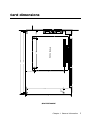
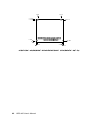
Card dimensions
Units=mm
Chapter 1 General Information
7
8
SBC-400 User's Manual
CHAPTER
Installation
2
This chapter tells how to set up the SBC400 hardware, including instructions on
setting jumpers and connecting peripherals, switches and indicators. Be sure to
read the all safety precautions before you
begin the installation procedure.
Chapter 2
Installation
9
Jumpers and connectors
Connectors on the board link it to external devices such as hard
disk drives, a keyboard or floppy drives. In addition, the board has
a number of jumpers that allow you to configure your system to
suit your application.
The table below lists the function of each of the board jumpers and
connectors.
Jumpers and connectors
Label
JP1
JP2,3,4
JP5,6
JP7,8
JP9
JP10
JP11
JP12
JP13
JP14
JP15
JP17
JP23,39
JP38
CN1
CN2
CN3
CN4
CN5,6
CN7
J1
COMA
COMB
10
Function
Cache memory select
CPU type select
CPU Vcc select
CPU clock select
Serial port IRQ select
Parallel port DRQ select
Parallel port DACK select
Power LED and keylock
External speaker
Reset switch
Turbo LED
Turbo switch
RS-232/422/485 select
Watchdog timer time-out signal select
Enhanced IDE connector
FDD connector
Parallel connector
Power connector
PC/104 module connectors
External keyboard connector
Keyboard and/or PS/2 mouse connector
Serial port 1
Serial port 2
SBC-400 User's Manual
Locating jumpers and connectors
COMA
MAX211
AMI BIOS
CN5
CN6
ALI
JP5,6
JP4
JP3
JP2
M1489
14.318
24MHz
SMC
FDC37C665
IMI
SC464
ODIN
M1487
JP7,8
CN2
JP39
JP38
ALI
JP10
JP9
OEC12C887
CN3
J1
MEGA-KB
16V8
JP12,13
JP23
COMB
MAX211
CN4
Data
RAM
Cache
32K8 CACHE RAM
32K8 CACHE RAM
32K8 CACHE RAM
32K8 CACHE RAM
Tag
RAM
Cache
JP1
SBC-400 486SX/DX/DX2/DX4 CPU CARD WITH CACHE REV:.A1
CPU
Socket
32K8 CACHE RAM
CN1
Chapter 2
SIMM
Socket
Installation
11
Setting jumpers
You configure your card to match the needs of your application by
setting jumpers. A jumper is the simplest kind of electric switch. It
consists of two metal pins and a small metal clip (often protected
by a plastic cover) that slides over the pins to connect them. To
“close” a jumper you connect the pins with the clip. To “open” a
jumper you remove the clip. Sometimes a jumper will have three
pins, labeled 1, 2 and 3. In this case you would connect either pins
1 and 2 or 2 and 3.
1
2
3
Open
Closed
Closed
2-3
The jumper settings are schematically depicted
in this manual as
follows:
1 2 3
Open
Closed
Closed 2-3
A pair of needle-nose pliers may be helpful when working with
jumpers.
If you have any doubts about the best hardware configuration for
your application, contact your local distributor or sales representative before you make any changes.
Generally, you simply need a standard cable to make most connections.
12
SBC-400 User's Manual
Safety precautions
Warning! Always completely disconnect the power cord
from your chassis whenever you are working on
it. Do not make connections while the power is
on, sensitive electronic components can be
damaged by the sudden rush of power. Only
experienced electronics personnel should open
the PC chassis.
Caution!
Always ground yourself to remove any static
charge before touching the CPU card. Modern
electronic devices are very sensitive to static
electric charges. Use a grounding wrist strap at
all times. Place all electronic components on a
static-dissipative surface or in a static-shielded
bag when they are not in the chassis.
Installing the CPU
The SBC-400 CPU card supports most 486 CPUs. The system's
performance depends on the CPU you choose. You can install or
upgrade the CPU in the board's PGA socket by following the
procedures outlined below. If your system has an existing CPU,
you need to remove it before installing the new CPU.
Removing a CPU
1. Disconnect power from the chassis, and unplug all connections
to the CPU card. Then, remove the CPU card from the chassis
by following the instructions in the user's manual for your
chassis.
2. Lift the CPU out of the PGA socket. The old chip may be
difficult to remove. You may find spray chip lubricant, designed
for pin-grid-array (PGA) devices, and a chip puller helpful.
These are available at electronics hobbyists' supply stores.
Chapter 2
Installation
13
Installing a CPU
To install the CPU, follow the instructions that came with it. If no
documentation was provided, the general procedure for installing a
CPU are outlined below:
1. Lubricate the pins on the CPU with lubricant for PGA devices.
This makes the CPU slide in much easier and greatly reduces
the chance of damaging the pins and other components.
2. Carefully align the CPU so that it is parallel to the socket. Make
sure that the notch on the corner of the CPU matches the notch
on the inside of the socket.
3. Gently push the CPU into the socket. There will probably be a
small gap between the CPU and the socket even when it is fully
seated. DO NOT USE EXCESSIVE FORCE!
When you install a new CPU, you may have to adjust other settings
on the board, such as CPU type, CPU clock and PCI speed, to
accommodate it. Make sure that the settings are correct for your
CPU. Improper settings may damage the CPU.
14
SBC-400 User's Manual
CPU type select (JP2, JP3, JP4)
JP2, JP3, and JP4 must be set to match the CPU type. The chart
below shows the proper jumper setting for their respective CPU.
CPU Type select (JP2, JP3, JP4)
Intel P24D
Cyrix MISC
JP
2
3
486DX/DX2/DX4-S 486SX-S
4
JP
2
3
4
JP
2
Pin 1
Pin 1
Pin 1
2
2
2
3
3
3
4
4
4
5
5
5
6
6
6
7
7
7
8
8
8
9
9
9
Cyrix/IBM/SGS
5x86
JP
Pin 1
2
2
3
3
4
4
5
5
6
6
7
7
8
8
9
9
2
3
4
4
Cyrix/IBM/SGS/TI486DX/DX2
486DX2
Pin 1
JP
3
2
3
4
JP
2
3
4
486SX
JP
2
Pin 1
Pin 1
2
2
3
3
4
4
5
5
6
6
7
7
8
8
9
9
AMD-X5-133/150 AMD DX4 Enhanced
AMD DX2
JP
JP
2 3 4
JP
2 3 4
AMD-X5-160
4
AMD DX4 Standard
2
3
4
JP
2
Pin 1
Pin 1
Pin 1
Pin 1
2
2
2
2
3
3
3
3
4
4
4
4
5
5
5
5
6
6
6
6
7
7
7
7
8
8
8
8
9
9
9
9
Chapter 2
3
Installation
3
4
15
CPU Vcc select (JP5, JP6)
JP5 and JP6 must be set to match the CPU type. The chart below
shows the proper jumper settings for their respective Vcc.
CPU Vcc select (JP5, JP6)
1
1
5.0 V
1
3.3 V
1
3.45 V
1
3.6 V
4.0 V
1
1
1
1
1
JP5
JP6
CPU clock select (JP7, JP8)
JP7 and JP8 are used to synchronize the CPU clock with the CPU
type. Set the CPU clock according to the base CPU speed.
CPU clock select (JP7, JP8)
25 MHz
50MHz
16
33 MHz
SBC-400 User's Manual
40 MHz
Installing DRAM (SIMMs)
The SBC-400 CPU card provides two 72-pin SIMM (Single In-line
Memory Module) sockets and supports between 1 MB to 128 MB
of RAM.
When installing SIMMs, make sure that Bank 1 is filled first.
Installing SIMMs
Note that the modules can only fit into a socket one way.
1. Insert the memory module into the socket at a moderate angle.
2. Push the module toward the vertical posts at both ends of the
socket until the module is upright, and the retaining clips at
both ends of the module click into place. When positioned
correctly, the pins on top of the vertical posts should correspond to the circular holes on the ends of the module.
3. Repeat steps 1 and 2 for each module you install.
Removing SIMMs
If you need to remove a SIMM, follow the procedures below:
1. Supporting the SIMM with a finger, use a pen or a similarly
shaped object and press one retaining clip straight down.
2. Repeat for the other side. When released, the retaining clips
will push the SIMM up and out of its upright position.
Chapter 2
Installation
17
3. Carefully pull the SIMM out of the socket with your fingers.
4. Repeat the above steps for each module you remove.
Selecting cache memory size
The SBC-400 features a 2nd level memory cache that supports
128, 256, or 512 KB of cache memory. Higher cache memory can
improve your system's performance.
The cache uses SRAM chips in three sizes: 32 KB, 64 KB and 128
KB. The on-board cache memory banks consists of four SRAM
chip sockets, each of which accepts one "Tag" chip. All SRAM
chips must have a speed of 20 ns or faster. The table below shows
the possible cache configurations:
Cache Configuration
Cache size
128 KB
256 KB
512 KB
Tag RAM
Data RAM
one 32 K x 8
four 32 KB x 8 SRAMs
one 32 K x 8
four 64 KB x 8 SRAMs
one 32 K x 8
four 128 K x 8 SRAMs
Cache memory select (JP1)
When the cache size changes, you must make sure that JP1 is set to
match the new cache memory size. The following chart shows the
proper jumper setting for each cache configuration:
1
2
1
2
3
4
3
4
Cache
memory
select
(JP1)
128 KB
18
256 KB
SBC-400 User's Manual
1
2
3
4
512 KB
IDE hard drive connections (CN1)
You can attach two Enhanced Integrated Device Electronics hard
disk drives to the SBC-400's internal controller. The card comes
with a 40-pin flat-cable piggyback cable. This cable has three
identical 40-pin flat-cable connectors.
Connecting the hard drive
Wire number 1 on the cable is red or blue, and the other wires are
gray.
1. Connect one end of the cable to CN1 on the CPU card. Make
sure that the red (or blue) wire corresponds to pin 1 on the
connector, which is labeled on the board (on the right side).
2. Plug the other end of the cable to the Enhanced IDE hard drive,
with pin 1 on the cable corresponding to pin 1 on the hard
drive. (See your hard drive's documentation for the location of
the connector.)
Unlike floppy drives, you can make the connections with any of the
connectors on the cable. If you install two drives, you will need to
set one as the master and one as the slave. You do this using
Chapter 2
Installation
19
jumpers on the drives. If you install just one drive, set it as the
master.
Pin assignments
The following table lists the pin numbers and their respective
signals:
Enhanced IDE connector (CN1)
Pin
1
3
5
7
9
11
13
15
17
19
21
23
25
27
29
31
33
20
Signal
Reset
D7
D6
D5
D4
D3
D2
D1
D0
GND
N.C,
IOW
IOR
IORDY
N.C.
IRQ
A1
Pin
2
4
6
8
10
12
14
16
18
20
22
24
26
28
30
32
34
SBC-400 User's Manual
Signal
GND
D8
D9
D10
D11
D12
D13
D14
D15
N.C.
GND
GND
GND
BALE
GND
-I/O CS16
N.C.
35
37
39
A0
CS0
-ACT
36
38
40
A2
CS1
GND
Floppy drive connections (CN2)
You can attach up to two floppy disks to the SBC-400's on-board
controller. You can use any combination of 5.25" (360 KB and
1.2 MB) and/or 3.5" (720 KB, 1.44 MB, and 2.88 MB) drives.
The SBC-400 CPU card comes with a 34-pin daisy-chain drive
connector cable. On one end of the cable is a 34-pin flat-cable
connector. There are two sets of floppy disk drive connectors,
one in the middle, and one on the other end. Each set consists of
a 34-pin flat-cable connector (usually used for 3.5" drives) and a
printed-circuit board connector (usually used for 5.25" drives).
Connecting the floppy drive
1. Plug the 34-pin flat-cable connector into CN2 on the CPU
card.
2. Attach the appropriate connector on the other end of the cable
to the floppy drive(s). You can use only one connector in the
set. The set on the end (after the twist in the cable) connects
to the A: floppy. The set in the middle connects to the B:
floppy.
Pin assignments
The following table lists the pin assignments for CN2:
Floppy disk connector (CN2)
Pin
Signal
1~33 (odd)
GND
4, 6
Unused
10
Motor enable A
14
Driver select A
18
Direction
22
Write data
Pin
8
12
16
24
Signal
2
High density
Index
Driver select B
Motor enable B
20
Step pulse
Write enable
Chapter 2
Installation
21
26
30
34
Track 0
Read data
Disk change
28
32
Write protect
Select head
Parallel port (CN3)
Normally, the parallel port is used to connect the card to a printer.
The SBC-400 includes an on-board parallel port, CN3, which is
accessed through a 26-pin flat-cable connector. The CPU card
comes with an adapter cable, which lets you use a traditional DB25 connector. The cable has a 26-pin connector on one end and a
DB-25 connector on the other, mounted on a retaining bracket.
Installing the retaining bracket
The retaining bracket installs at an empty slot in your system's
chassis. It provides an external port that allows your parallel
peripheral to access to the card's parallel port connector.
1. Find an empty slot in your chassis.
2. Unscrew the plate that covers the end of the slot.
3. Screw in the bracket in place of the plate.
4. Next, attach the flat-cable connector to CN3 on the CPU card.
Wire 1 of the cable is red or blue, and the other wires are gray.
Make sure that Wire 1 connects to Pin 1 of the PRINTER
connector. Pin 1 is on the right side of CN3.
Pin assignments
Parallel port connector (CN3)
Pin
1
3
5
7
9
22
Signal
Strobe
Data 1
Data 3
Data 5
Data 9
Pin
2
4
6
8
10
SBC-400 User's Manual
Signal
Data 0
Data 2
Data 4
Data 6
-Acknowledge
11
13
15
17
Busy
+ Select
- Error
- Select input
12
14
16
18~25
Paper empty
- Auto feed
- Init printer
GND
Parallel port DRQ (JP10) and DACK (JP11)
You can select the parallel port DRQ and DACK by setting JP10
and JP11, respectively. The following charts show the available
1
1
options.
Parallel port DRQ selection (JP10) and DACK selection (JP11)
Chapter 2
Installation
23
DRQ1/DACK1 (default)
JP10
JP11
DRQ3/DACK3
JP10
JP11
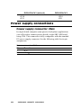
Power supply connections
Power supply connector (CN4)
In single-board-computer (non-passive-backplane) applications
you will need to connect power directly to the SBC-400 board
using CN4. This connector is fully compatible with the standard
PC power supply connector. See the following table for its pin
assignments:
Power connector (CN4)
Pin
1
2
24
Function
N.C.
+5 V DC
SBC-400 User's Manual
3
4
5
6
+12 VDC
-12 V DC
GND
GND
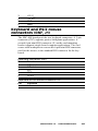
Keyboard and PS/2 mouse
connectors (CN7, J1)
The SBC-400 board provides two keyboard connectors. A 5-pin
connector (CN7) supports passive backplane applications. A
second 6-pin mini-DIN connector (J1) on the card mounting
bracket supports single-board-computer applications. The card
comes with an adapter to convert the 6-pin mini-DIN connector,
used for the mouse, to the standard DIN connector for the keyboard.
Keyboard connector (CN7)
Pin
1
2
3
4
5
Function
K.B. clock
K.B. data
N.C.
GND
+5 V DC
Keyboard or PS/2 mouse connector (J1)
Pin
1
Function
K.B. data
Chapter 2
Installation
25
2
3
4
5
6
PS/2 mouse data
GND
+5 V DC
K.B. clock
PS/2 mouse clock
Serial ports
The SBC-400 offers two serial ports: one RS-232 and one RS-232/
422/485. Using the BIOS Peripheral Setup program, you can select
the address for each port or disable it.
The card mounting bracket has two serial port connectors. The DB9 connector on the top of the bracket is COMA, the RS-232 serial
port. The DB-9 connector on the bottom of the bracket is COMB,
the RS-232/422/485 serial port.
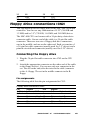
RS-232/422/485 select for COMB (JP23, JP39)
RS-232 serial ports are widely used for external input/output
devices. The RS-422 and RS-485, however, are popular for
industrial and laboratory applications because they offer high noise
resistance and long range communication (up to 4000 ft, 1200 m).
The RS-422 is communly used for two-way communication
between two devices, where as RS-485 is used for communication
between a single master and a network of slave modules.
COMA is the RS-232 serial port, and COMB can function as an
RS-232, RS-422, or RS-485, depending on the jumper settings for
JP23 and JP39. To1select the desired serial port type for COMB,
adjust JP23 and JP39 as follows:
1
RS-232/422/485 select for COMB (JP23, JP39)
JP23
RS-232
26
1
SBC-400 User's Manual
JP39
RS-422
RS-485
RS-232/422/485 serial port connections
(COMA, COMB)
Pin assignments
The following table shows the pin assignments for the card's RS232 and RS-422/485 (COMB) serial port connectors:
RS-232 (COMA, COMB)
RS-422/485 (COMB)
Pin
1
2
3
4
5
6
7
8
9
Pin
1
2
3
4
5
6
7
8
9
Signal
DCD
RX
TX
DTR
GND
DSR
RTS
CTS
RI
Signal
TX- (DTE)
TX+ (DTE)
RX+ (DTE)
RX- (DTE)
Ground
RTSRTS+
CTSCTS-
RS-422 signal wiring
RS-422 is used for long-distance point-to-point connections. RS422 originally used four wires for one-way communication (with
devices such as display terminals or printer) but was later adopted
Chapter 2
Installation
27
by the industry for simultaneous two-way communication by
doubling the number of wires.
Each pin on the first device connects to a corresponding device on
the second. Flow control lines manage the communication. The
following table shows pin connections.
Computer A
Pin
1
2
3
4
5
6
7
8
9
Signal
TXTX+
RX+
RXGround
RTSRTS+
CTS+
CTS-
Computer B
>
>
<
<
<
>
>
<
<
Pin
4
3
2
1
5
9
8
7
6
Signal
RXRX+
TX+
TXGround
CTSCTS+
RTS+
RTS-
RS-485 signal wiring
In a typical RS-485 application, the host device requests data from
a slove module then listens for the response. The host transmits and
receives data on the same pair of wires. Software handles the flow
control; no other wires are needed.
Pin assignments appear in the following table. Pins 1 and 4 share
the Date+ wire. Pins 2 and 3 share the Data- wire.
Computer A
28
SBC-400 User's Manual
Device B
Pin
Signal
1
4
TXRX-
2
3
5
TX+
RX+
Ground
]
Data-
[
]
Data+
[
Pin
Signal
1
4
TXRX-
2
3
5
TX+
RX+
Ground
Serial ports IRQ select (JP9)
You can select the serial ports' IRQs by setting JP9 as follows:
Serial ports IRQ selection (JP9)
COMA
COMB
IRQ3
IRQ4
IRQ4
IRQ3
JP9 setting
Chapter 2
Installation
29
IRQ11
IRQ12
IRQ12
IRQ11
Watchdog timer setup
Watchdog timer time-out
signal select
(JP38)
1 2 3
1
2
3
If CPU processing comes to a halt because of EMI or software bug,
the watchdog timer can either reset the CPU or signal an interrupt
on IRQ15.
Watchdog timer time-out signal select (JP38)
Reset CPU
IRQ15
Watchdog timer programming
The watchdog timer must be programmed to write to I/O port
address 443 at an interval shorter than the timer's preset interval.
The timer's interval has a tolerance of ±5%, so you should program
an instruction that will refresh the timer before a time-out occurs.
30
SBC-400 User's Manual
The following steps illustrate how you might program the watchdog timer.
1. Write to I/O port 443 (Hex) and designate a time-out interval.
This will enable the watchdog and set up its time-out interval.
2. Write to I/O port 043 (Hex) and any random value. This will in
turn disable the watchdog timer.
The watchdog timer-out interval can be set at 16 levels between 2
and 32 seconds. The following table shows the Hex values for the
appropriate time-out intervals:
Watchdog timer delay values
Delay time
0~2
2~4
Value (Hex)
F
E
Delay time
16~18
18~20
Chapter 2
Value (Hex)
7
6
Installation
31
4~6
6~8
8~10
10~12
12~14
14~16
D
C
B
A
9
8
20~22
22~24
24~26
26~28
28~30
30~32
5
4
3
2
1
0
External Switches and LEDs
Power LED and keylock (JP12)
You can connect an LED to indicate when the CPU card is on.
Pin 1 of JP12 supplies power to the LED and Pin 3 is the ground.
You can use a switch (or a lock) to disable the keyboard. In this
state the PC will not respond to any input. This is useful if you
don’t want anyone to change or stop a running program. Simply
connect the switch between Pins 4 and 5. The pin assignments
appear in the following table:
Power LED and keylock (JP12)
Pin
5
4
3
2
1
Function
LED Power (+5 V)
No Connector
Ground
Keyboard lock
Ground
External speaker (JP13)
The CPU card has its own buzzer. You can disable the internal
buzzer and connect an external speaker to JP13. Enabling the
external speaker automatically disables the internal buzzer.
32
SBC-400 User's Manual
External speaker (JP13)
Pin
5
4
3
2
1
Function
Vcc
Speaker output
Buzzer in
Speaker output
NC
Reset switch (JP14)
You can connect an external switch to easily reset your computer.
This switch restarts your computer as if you had turned off the
power then turned it back on. The following table shows the pin
assignments for the JP14.
Reset switch (JP14)
Pin
1
2
Function
Ground
Reset
Turbo LED (JP15)
You can connect a LED indicator across JP15 to indicate when the
CPU is in Turbo mode. Marks on the circuit board indicate LED
polarity (the pin on the left is positive).
Turbo LED (JP15)
Pin
1
2
Function
Turbo
Ground
Turbo switch (JP17)
You can connect a switch across the pins of JP17 to change the
CPU speed between Turbo and non-Turbo mode. When you leave
the pins open, the CPU card operates at full speed. When you close
the pins, the card operates at slow speed for compatibility with
older software.
Turbo switch (JP17)
Pin
1
2
Function
- Deturbo
Pull low
Low speed
Chapter 2
High Speed
Installation
33
34
SBC-400 User's Manual
CHAPTER
3
AMI WinBIOS Setup
This chapter describes the card’s diagnostic tests and how to set BIOS configuration data in a Windows environment.
Chapter 3 AMI WinBIOS setup
35
General information
WinBIOS Setup configures system information that is stored in
CMOS RAM. Unlike conventional BIOS setup programs, WinBIOS features a graphical user interface that is easy to use.
Starting WinBIOS setup
As POST executes, the following appears;
Hit <DEL> if you want to run SETUP
Press <DEL> to run WinBIOS setup.
WinBIOS main menu
The WinBIOS setup screen appears as follows:
36
SBC-400 User's Manual
Using a mouse with WinBIOS setup
WinBIOS Setup can be accessed via keyboard, mouse, or pen. The
mouse click functions are:
• single click to change or select both global and current fields
• double click to perform an operation in the selected field
Using the keyboard with WinBIOS setup
WinBIOS Setup has a built-in keyboard driver that uses simple
keystroke combinations:
Keystroke
<tab>
è, ç, é , ê
Function
Move to the next window or field.
Move to the next field to the right, left,
above, or below.
<ENTER>
Select in the current field.
+
Increments a value.
Decrements a value.
<ESC>
Closes the current operation and return to
previous level.
<PgUp>
Returns to the previous page.
<PgDn>
Advances to the next page.
<Home>
Returns to the beginning of the text.
<End>
Advances to the end of the text.
<ALT>+H
Access a help window.
<ALT>+<Spacebar>Exit WinBIOS Setup.
Alphabetic keys A to Z are used in the Virtual keyboard, and
are not case sensitive.
Numeric keys
0 to 9 are in the Virtual keyboard and
Numerickeypad.
Chapter 3 AMI WinBIOS setup
37
Setup
Standard Setup
The WinBIOS Setup options described in this section are selected
by choosing the Standard icon from the WinBIOS Setup main
menu selection screen, as shown below.
The Standard Setup screen appears:
Date, Day and Time Configuration
Select the Date and Time icon in the Standard setup. The current
values for each category are displayed. Enter new values through
the keyboard.
Floppy A, Floppy B
Select these icons to configure the type of floppy drive that is
attached to the system: 360 KB 5¼", 1.2 MB 5¼", 720 KB 3½",
1.44 MB 3½", and/or 2.88 MB 3½". The settings have not been
pre-installed.
Master Disk, Slave Disk
Select these icons to configure the hard disk type you are using for
the master and the slave. The settings have not been pre-installed.
Type in 1~46, User, ESDI, or SCSI.
38
SBC-400 User's Manual
Advanced Setup
Select the Advanced icon from the WinBIOS Setup main menu to
enter Advanced setup.
The Advanced Setup options described in this section are the
standard options as shown on the following screen.
Typematic Rate (Char/Sec)
Typematic Rate sets the rate at which characters on the screen
repeat when a key is pressed and held down. The settings are 15,
20, 24, 30 characters per second.
System Keyboard
This option specifies if error messages are displayed if a keyboard
is not attached. This permits you to configure workstations with no
keyboards. The settings are Absent or Present.
Primary Display
Select this icon to configure the type of monitor attached to the
computer. The settings are Monochrome, Color 40 x 25, Color
80x25, VGA/PGA/EGA/, or Not Installed.
Above 1 MB Memory Test
When this option is enabled, the WinBIOS memory test is performed on all system memory. When disabled, the memory test is
done only on the first 1 MB of system memory.
Chapter 3 AMI WinBIOS setup
39
Memory Test Tick Sound
This option enables (turns on) or disables (turns off) the ticking
sound during the memory test.
Memory Parity Error Check
This option enables or disables parity error checking for system
RAM. The settings are Enabled (all system RAM parity is
checked) or Disabled (parity is checked only on the first 1 MB of
system RAM).
Hit <Del> Message Display
Disabling this option prevents the message
Hit <DEL> if you want to run Setup
from appearing when the system boots. The settings are Enabled or
Disabled.
Extended BIOS RAM Area
Specify in this option if the top 1 KB of the system programming
area beginning at 639 K or 0:300 in the system BIOS area in low
memory will be used to store hard disk information. The settings
are Top 1 K or 0:300.
Wait for <F1> If Any Error
WinBIOS POST runs system diagnostic tests that can generate a
message followed by:
Press <F1> to continue
If this option is enabled, WinBIOS waits for the end user to press
<F1> before continuing. If this option is disabled, WinBIOS
continues the boot process without waiting for <F1> to be pressed.
System Boot Up Num Lock
When On, this option turns off Num Lock when the system is
powered on so the end user can use the arrow keys on both the
numeric keypad and the keyboard.
40
SBC-400 User's Manual
Floppy Drive Seek at Boot
When this option is enabled, WinBIOS performs a Seek command
on floppy drive A: before booting the system.
System Boot Up Sequence
This option sets the sequence of boot drives (either floppy drive A:
or hard disk drive C:) that WinBIOS attempts to boot from after
POST completes. The settings are C:, A: (first C:, then A:) or A:,C:
(first A:, then C:).
System Boot Up CPU Speed
This option sets the speed of the CPU at system boot time. The
settings are High or Low.
External Cache
This option enables secondary cache memory. If Both is selected,
internal cache and external cache memory is enabled. If Internal is
chosen, only the internal cache memory in the Pentium CPU is
enabled. If Disabled is chosen, all cache memory in the Pentium
CPU is disabled.
External Cache Mode
This option selects the type of caching algorithm used by WinBIOS
and the computer for L2 (external) secondary cache memory. The
settings are Wr-Thr (Write-Through) or Wr-Back (Write-Back).
Turbo Switch function
When this option is set to Enabled, the externally mounted turbo
switch is enabled.
Password Checking
This option enables the password check option every time the
system boots or the end user runs Setup. If Always is chosen, a user
password prompt appears every time the computer is turned on. If
Setup is chosen, the password prompt appears if WinBIOS is
executed. The Optimal and Fail-Safe default settings are Setup.
Video ROM Shadow C000,32K
Chapter 3 AMI WinBIOS setup
41
When this option is enabled, the video ROM area from C0000h C7FFFh is copied (shadowed) to RAM for faster execution. The
settings are Absent, NoShadow, or Shadow.
Shadow
Shadow
Shadow
Shadow
Shadow
Shadow
C800,16K
CC00,16K
D000,16K
D400,16K
D800,16K
DC00,16K
These options enable shadowing of the contents of the ROM area
in the option title. The settings are Absent, NoShadow, or Shadow.
The ROM area that is not used by ISA adapter cards will be
allocated to PCI adapter cards.
Auto KeyLock Timeout
This option sets the timeout value for the WinBIOS AutoKeyLock
feature. If Password support is enabled, AutoKeyLock automatically locks the keyboard and mouse if there has been no system
activity for the length of time specified in this option. The settings
are Disabled, 1 Min., 2 Min., 3 Min., 4 Min., 5 Min., 6 Min., 7
Min., 8 Min., 9 Min., 10 min., 11 Min., 12 Min., 13 Min., 14 Min.,
15 Min. The Optimal and Fail-Safe defaults are Disabled.
42
SBC-400 User's Manual
Chipset Setup
The WinBIOS Setup options described in this section are selected
by choosing the Chipset icon from the WinBIOS setup main menu,
shown below.
The following is a list options offered by Chipset Setup
Chipset setup options
Function
Auto Configuration Function
DRAM Read Timing
DRAM Write Timing
SRAM Read Timing
Options
Disabled/Enabled
7.16
CPU Bus Speed/3
CPU Bus Speed/4
CPU Bus Speed/5
CPU Bus Speed/6
CPU Bus Speed/8
Slow
Normal
Faster
Fastest
Slow
Normal
Faster
Fastest
2-1-1-1
3-1-1-1
3-2-2-2
4-2-2-2
Chapter 3 AMI WinBIOS setup
43
Function
SRAM Write Timing
Parity check
Hidden Refresh
Cyrix CPU L1 Cache Mode
ISA I/O Recovery
CPU to PCI Write Buffer
Byte Merge
Fast Back to Back
C x 5 x 86 Linear Wrapped Mode
PCI IDE Trigger Type
44
SBC-400 User's Manual
Options
0W
1W
Disabled
Enabled
Disabled
Enabled
WT (Write-through)
WB (Write-back)
Disabled
Enabled
Disabled
Enabled
Disabled
Enabled
Disabled
Enabled
Disabled
Enabled
Edge
Level
Power Management Setup
As part of the "Green" function, the Power Management setup
offers options to help reduce power consumption. To see the the
options in this group, choose the Power Mgmt icon from the
WinBIOS Setup main menu.
Chapter 3 AMI WinBIOS setup
45
Peripheral Setup
To access Peripheral Setup, select the Peripheral icon in the
WinBIOS main menu. The following screen appears:
Programming Option
Auto
When set to Auto, WinBIOS automatically detects all adapter cards
installed in the system and configures the onboard I/O (serial ports,
parallel ports, floppy controllers, and IDE controller). All other
Peripheral Setup option settings are ignored. Any serial port,
parallel port, floppy controller or IDE (Integrated Drive Electronics) controller on an adapter card in an expansion slot is configured
before onboard I/O.
In addition, WinBIOS also attempts to avoid IRQ conflicts. If the
offboard serial ports are configured to specific starting I/O ports
via jumper settings, WinBIOS configures the onboard serial ports
to avoid conflicts. For example, if the default serial port starting I/
O ports (serial port1 - 3F8h, serial port2 - 2F8h, serial port3 3E8h, serial port4 - 2E8h) are, the configurations listed in the
following table are possible:
46
SBC-400 User's Manual
Offboard serial port configuration
# of ports
2
2
1
1
port assignment
3E8h and 2F8h
3F8h and 3E8h
2F8h
3F8h
onboard serial ort
3E8h and 3E8h
3F8h and Disabled
3F8h and Disabled
2F8h and Disabled
Manual
If Manual is selected, the settings chosen by the end user in the
Peripheral Setup apply. WinBIOS will report any I/O conflicts after
display the BIOS Configuration summary screen.
Onboard FDC
This option enables the use of the floppy drive controller on the
motherboard (if installed). The settings are Enabled or Disabled.
Onboard IDE
This option enables the use of the IDE controller on the motherboard, if installed. The settings are enabled or Disabled.
First Serial Port Address
IRQ4 is used for the first serial port (COM1). This option enables
serial port 1 on the motherboard, if installed. The settings are
2E8h.
Second Serial Port Address
IRQ3 is used for the second serial port (COM2). This option
enables the serial port 2 on the motherboard, if installed. The
settings are 2E8h.
Parallel Port Address
IRQ7 is used for the parallel port (LPT1). The IRQ can be changed
to IRQ5. This option enables the parallel port on the motherboard,
if installed. The settings are 278h.
Parallel Port Mode
This option specifies the parallel port Mode. The settings are
Normal or Extended.
Chapter 3 AMI WinBIOS setup
47
Utility
The following icons appear in this section:
Detect C:
If drive C: is an IDE drive, the hard disk drive parameters for drive
C: are automatically detected and reported to the Hard Disk Drive
C: screen in Standard Setup, so you can easily configure drive C:.
Detect D:
If drive D: is an IDE drive, the hard disk drive parameters for drive
D: are automatically detected and reported to the Hard Disk Drive
D: screen in Standard Setup, so you can easily configure drive D:.
Color Set
This option sets the WinBIOS Setup screen colors.
48
SBC-400 User's Manual
Security
The following icons appear in this section:
WinBIOS password support
WinBIOS Setup has an optional password feature. The system can
be configured so that all users must enter a password every time the
system boots or when WinBIOS Setup is executed. The following
screen appears when you select the password icon.
You can enter a password by:
• typing the password on the keyboard
• selecting each letter via the mouse
• selecting each letter via the pen stylus (pen access must be
customized for each specific hardware platform.)
Chapter 3 AMI WinBIOS setup
49
Setting a Password
The password check option is enabled in Advanced Setup by
choosing either Always or Setup. Here, you determine the password
to be used. The password is stored in CMOS RAM.
To assign a password,
1. Enter a 1-6 character password. The password does not appear
on the screen when typed.
2. Retype the password when prompted by WinBIOS.
A message box will appear when the password is confirmed.
Keep a record of the password. If you forget the password, you
must drain CMOS RAM and reconfigure the system.
Changing a password
1. Select the Password icon from the Security section of the
WinBIOS Setup main menu.
2. Enter the password and press <ENTER>. The screen does not
display the characters entered.
3. After the new password is entered, retype the new password as
prompted and press <ENTER>.
If the password confirmation is incorrect, an error message
appears. If the new password is entered without error, press <ESC>
to return to the WinBIOS setup Main Menu. The password is
stored in CMOS RAM after WinBIOS Setup completes. The next
time the system boots, you are prompted for the password if the
password function is present and is enabled.
50
SBC-400 User's Manual
Anti-virus
Select the Anti-virus icon from the Security section of the WinBIOS Setup main menu. WinBIOS issues a warning when any
program (or virus) issues a Disk format command or attempts to
write to the boot sector of the hard disk drive. The settings are
Enabled or Disabled.
If enabled, the following appears when a write is attempted to the
boot sector. You may have to type N several times to prevent the
boot sector write.
Boot Sector Write !!!
Possible VIRUS: Continue (Y/N)?
_
The following is displayed after any attempt to format any cylinder,
head, or sector of any hard disk drive via the BIOS INT 13 Hard
Disk Drive Service:
Format!!!
Possible VIRUS: Continue (Y/N)? _
Chapter 3 AMI WinBIOS setup
51
Default
The icons in this section permit you to select a group of settings for
all WinBIOs Setup options. Not only can you use these icons to
quickly set system configuration parameters, you can choose a
group of settings that have a better chance of working when the
system is having configuration-related problems.
Original
Choose the Original icon to return to the system configuration
values present in WinBIOS Setup when you first began this
WinBIOS Setup session.
Optimal
You can load the optimal default settings for the WinBIOS Setup
options by selecting the Optimal icon. The Optimal default settings
are best-case values that should optimize system performance. If
CMOS RAM is corrupted, the Optimal settings are loaded automatically.
Fail-Safe
You can load the Fail-Safe WinBIOS Setup options settings by
selecting the Fail-Safe icon.
The Fail-Safe settings provide the most stable settings, though they
do not provide optimal performance. Use this option as a diagnostic aid if the system is behaving erratically.
52
SBC-400 User's Manual
Exiting WinBIOS
You can exit WinBIOS by pressing the <ESC> key while in
theWinBIOS main menu screen.
The following screen appears:
Select the option you desire, and the system will continue its
bootup sequence.
Chapter 3 AMI WinBIOS setup
53
54
SBC-400 User's Manual
APPENDIX
A
Watchdog Timer
Demo Program
The following demo program illustrates
the programming steps required to enable,
set, and disable the watchdog timer.
Appendix A Watchdog Timer Demo Program
55
#include<stdio.h> #include<dos.h> #include<conio> #include
<time.h> #include<graphics.h> void mydelay(void);
/* MAIN PROGRAM */ void main (void) {
unsigned int
dog=0
run_time=0;
char inkey;
clrscr();
gotoxy(15, 6);printf("AAEON TECHNOLOGY, INC.");
gotoxy(15, 7);printf("WATCHDOG TIMER TEST & DEMO
PROGRAM");
gotoxy(15, 9);printf("Please setup watchdog delay
time:(2 Sec-30 Sec)");
/* Set watchdog timer time-out interval */
scanf("%2d",&dog);
/* Input watchdog timer timeout interval (Sec) */
dog=dog/2;
/* Convert time-out interval
to designated Hex */
dog=15-dog;
outportb (0x443,dog); /* Enable watchdog timer */
/* Setup screen display format */
gotoxy(15,11);printf("Now enable watchdog!");
gotoxy(15,12);printf("You can put keyboard reset or
disable watchdog.");
gotoxy(15,13);printf(" [1]. Reset watchdog.");
gotoxy(15,14);printf(" [2]. Disable watchdog.");
gotoxy(15,15);printf(" [3]. Return to O.S.");
/* Read key pressed */
while(1){
if(kbhit()){
inkey=getch();
switch(inkey){
case '1': /* Reset Watchdog timer */
gotoxy(15,11);printf("Now enable
watchdog timer!");
outportb(0x443,dog);
run_time=0;
break;
case '2': /* Disable Watchdog timer */
gotoxy(15,12);printf("Now
disable watchdog timer!");
outportb (0x43,dog);
return;
default : break;
}
}
56
SBC-400 User's Manual
mydelay();
run_time=run_time+1;
/* Display time elapsed */
gotoxy(45,11);printf(%2d.%1d sec",run_time/
10,run_time%10);
}
}
/* USER FUNCTION LIBRARY */ void mydelay(void) /*
Delay program: */ /* Delay 109.89ms (18.2Hz*2) */{
clock_t start,end;
start=clock();
end=start;
while((end-start)<2){
end=clock();
}
}
Appendix A Watchdog Timer Demo Program
57
58
SBC-400 User's Manual
APPENDIX
B
Installing PC/104
Modules
This appendix gives instructions for
installing PC/104 module.
Appendix B Installing PC/104 Modules
59
Installing PC/104 modules
The SBC-400's PC/104 connectors give you the flexibility to attach
PC/104 expansion modules. These modules perform the functions
of traditional plug-in expansion cards, but save space and valuable
slots. Modules include:
• PCM-3290
GPS Module
• PCM-3810
Solid-state Disk Module
• PCM-3820
High Density Flash Disk Module
• PCM-3110
PCMCIA Module
• PCM-3111
Secondary PCMCIA Module
• PCM-3610
Isolated RS-232 and RS-422/485 Module
• PCM-3660
Ethernet Module
• PCM-3718
30 KHz A/D Module
• PCM-3724
48-channel DIO Module
• PCM-3910
Breadboard Module
To install these modules on the SBC-400 is a quick and simple
operation. The following steps show how to mount the PC/104
modules:
Step 1
Remove the SBC-400 from your system paying
particular attention to the safety instructions already
mentioned above.
Step 2
Make any jumper or link changes required to the CPU
card now. Once the PC/104 module is mounted you
may have difficulty in accessing these.
Step 3
Normal PC/104 modules have "male" connectors and
mount directly onto the main card. However, for
reasons that ensure better bus matching, the connectors
on the SBC-400 and the PC/104 module are both
"female". For this reason you need to plug-in a "malemale" adapter connecter (included with the SBC-400).
Please refer to the following PC/104 module mounting
diagram on the following page. After this is in place
you then have the correct mounting connector to accept
your PC/104 module.
60
SBC-400 User's Manual
Step 4
Mount the PC/104 module onto the CPU card. Do this
by pressing the module firmly but carefully onto the
mounting connectors.
Step 5
Secure the PC/104 module onto the CPU card using the
four mounting spacers and srews.
PC/104
Mounting Support
Female
S B C -400
350A
CPU Card
Male
Male
PC/104 Mounting
Adaptor
Female
Male
PC/104 Module
PC/104 Module Mounting Diagram
Appendix B Installing PC/104 Modules
61
3.500
3.250
3.775
3.575
3.575
0.200
0.200
0
0.200
0
3.350
3.550
PC/104 module dimensions (inches ±5 %)
62
SBC-400 User's Manual