1
CD-RW5000
SERVICE MANUAL
No. S9071CDRW5000
AUDIO TOWER SYSTEM
MODEL CD-RW5000
CD-RW5000 Audio Tower System consisting of CD-RW5000 (main
unit) and CP-RW5000 (speaker system).
• In the interests of user-safety the set should be restored to its original
condition and only parts identical to those specified should be used.
CONTENTS
Page
IMPORTANT SERVICE NOTES (FOR U.S.A. ONLY) ...................................................................................................... 2
SPECIFICATIONS ............................................................................................................................................................ 2
NAMES OF PARTS .......................................................................................................................................................... 3
OPERATION MANUAL ..................................................................................................................................................... 5
DISASSEMBLY ................................................................................................................................................................. 8
REMOVING AND REINSTALLING THE MAIN PARTS .................................................................................................. 11
CD CHANGER MECHANISM MAIN BASE PARTS ASSEMBLING/ADJUSTING PROCEDURE ................................. 13
ADJUSTMENT ................................................................................................................................................................ 20
TEST MODE ................................................................................................................................................................... 21
ERROR MESSAGE LIST ................................................................................................................................................ 24
NOTES ON SCHEMATIC DIAGRAM ............................................................................................................................. 25
TYPES OF TRANSISTOR AND LED .............................................................................................................................. 25
BLOCK DIAGRAM .......................................................................................................................................................... 26
SCHEMATIC DIAGRAM ................................................................................................................................................. 32
WIRING SIDE OF P.W.BOARD ...................................................................................................................................... 43
WAVEFORMS OF CD CIRCUIT ..................................................................................................................................... 52
TROUBLESHOOTING .................................................................................................................................................... 53
FUNCTION TABLE OF IC .............................................................................................................................................. 56
LCD DISPLAY ................................................................................................................................................................. 62
PARTS GUIDE/EXPLODED VIEW
PACKING OF THE SET (FOR U.S.A. ONLY)
SHARP CORPORATION
This document has been published to be used
for after sales service only.
The contents are subject to change without notice.
CD-RW5000
FOR A COMPLETE DESCRIPTION OF THE OPERATION OF THIS UNIT, PLEASE REFER
TO THE OPERATION MANUAL.
IMPORTANT SERVICE NOTES (FOR U.S.A. ONLY)
BEFORE RETURNING THE AUDIO PRODUCT
(Fire & Shock Hazard)
Before returning the audio product to the user, perform the
following safety checks.
1. Inspect all lead dress to make certain that leads are not
pinched or that hardware is not lodged between the chassis
and other metal parts in the audio product.
2. Inspect all protective devices such as insulating materials,
cabinet, terminal board, adjustment and compartment covers
or shields, mechanical insulators etc.
3. To be sure that no shock hazard exists, check for leakage
current in the following manner.
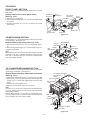
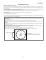
* Plug the AC line cord directly into a 120 volt AC outlet.
* Using two clip leads, connect a 1.5k ohm, 10 watt resistor
paralleled by a 0.15µF capacitor in series with all exposed
metal cabinet parts and a known earth ground, such as
conduit or electrical ground connected to earth ground.
* Use a VTVM or VOM with 1000 ohm per volt, or higher,
sensitivity to measure the AC voltage drop across the
resistor (See diagram).
* Connect the resistor connection to all exposed metal parts
having a return path to the chassis (antenna, metal cabinet,
screw heads, knobs and control shafts, escutcheon, etc.)
and measure the AC voltage drop across the resistor.
VTVM
AC SCALE
1.5k ohms
10W
0.15µF
TEST PROBE
TO EXPOSED
METAL PARTS
CONNECT TO
KNOWN EARTH
GROUND
All tests must be repeated with the AC line cord plug connection
reversed.
Any reading of 0.3 volt RMS (this corresponds to 0.2 milliamp.
AC.) or more is excessive and indicates a potential shock
hazard which must be corrected before returning the audio
product to the owner.
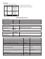
SPECIFICATIONS
CD-RW5000
■ Tuner
■ General
Power source
AC 120 V, 60 Hz
Power consumption
200 W
Dimensions
Width: 7-7/8" (200 mm)
Height: 13-7/8" (352 mm)
Depth: 14-7/8" (377 mm)
Weight
23.8 lbs (10.8 kg)
Frequency range
■ CD-R
Type
■ Amplifier
Output power
100 watts minimum RMS into 6 ohms from 60 Hz to 20
kHz, 10 % total harmonic distortion
Subwoofer : 60 W/ch
(60 Hz - 200 Hz, 6 ohms, 10 % T.H.D.)
FM: 87.5-108.0 MHz
AM: 530-1,720 kHz
1-disc compact disc recorder/player
Signal readout
Non-contact, 3-beam semiconductor laser pickup
Rotational speed
200-500 rpm CLV
Error correction
CIRC (Cross Interleave Reed-Solomon Code)
Quantization
16-bit linear
Filter
64 fs digital interpolation filter
Main : 40 W/ch
(200 Hz - 20 kHz, 6 ohms, 10 % T.H.D.)
Frequency response
20 - 20,000 Hz
D/A converter
1-bit D/A converter
Output terminals
Speakers: 6 ohms
Headphones: 16-50 ohms (recommended; 32 ohms)
Digital output (optical)
Dynamic range
90 dB (1 kHz) playback
84 dB (1 kHz) recording
Input terminals
Auxiliary: 500 mV/47 kohms
CP-RW5000
Phono: 2.5 mV (1 kHz)
Digital input (optical)
Type
3-way type speaker system
2" (5 cm) Tweeter
■ CD player
5-1/4" (13 cm) Woofer
Type
6-disc multi-play compact disc changer player
Signal readout
Non-contact, 3-beam semiconductor laser pickup
D/A converter
Frequency response
Dynamic range
5-1/4" (13 cm) Subwoofer
1-bit D/A converter
20 - 20,000 Hz
90 dB (1 kHz)
■ Cassette deck
Frequency response
50-14,000 Hz (Normal tape)
Signal/noise ratio
50 dB (recording/playback)
Wow and flutter
0.3 % (WRMS)
Maximum input power (Total)
200 W
Rated input power (Total)
100 W
Impedance
6 ohms
Dimensions
Width: 8-1/4" (210 mm)
Height: 15-7/16" (392 mm)
Depth: 13-9/16" (345 mm)
Weight
11.2 lbs. (5.1 kg)/each
Specifications for this model are subject to change
without prior notice.
–2–
CD-RW5000
CD-RW5000
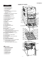
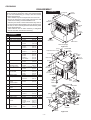
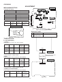
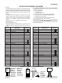
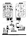
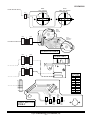
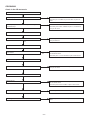
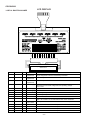
NAMES OF PARTS
■ Front panel
01.
02.
03.
04.
05.
06.
07.
08.
09.
10.
11.
12.
13.
14.
15.
16.
17.
18.
19.
20.
21.
22.
23.
24.
25.
26.
27.
28.
29.
30.
31.
32.
33.
34.
35.
36.
37.
38.
39.
Cassette Compartment
Volume Up/Demo Button
Volume Down Button
Timer Set Indicator
Power Button
CD Direct Play Buttons (with Indicator)/
CD Tray Eject Buttons
CD Trays
CD/CD-R/CD-RW Play Mode Select Button
CD-R/CD-RW Text Edit Button
Headphone Jack
CD-R/CD-RW Tray Eject Button
CD-R/CD-RW Tray
Control Panel Open/Close Button
Equalizer Mode Select Button
Extra Bass Button
Menu Button
Display/Character Button
Jog Dial
Enter Button
Delete Button
Tuner (Band) Button
CD-R/CD-RW Record Button
CD Button
CD Track Edit Button
CD-R Button
CD CD-R One Touch Edit Button
CD-R/CD-RW Finalize Button
CD/CD-R/CD-RW Fast Reverse, Tape Fast Wind
or Tuning Down Button (with Indicator)
Stop Button (with Indicator)
Tape Reverse Play Button (with Indicator)
Tape Button
CD-R/CD-RW Record Mode Button
Auxiliary Button
CD-R/CD-RW Record Speed Select Button
Erase Button
CD-R/CD-RW Auto Mark Button
Tape Record Pause Button
CD/CD-R/CD-RW Fast Forward, Tape Fast Wind
or Tuning Up Button (with Indicator)
CD/CD-R/CD-RW Play or Pause/
Tape Forward Play Button (with Indicator)
■ Rear panel
01.
02.
03.
04.
05.
06.
07.
08.
09.
AM Loop Antenna Terminal
Antenna Ground Terminal
FM Antenna Terminal
Auxiliary Input Jacks
Phono Input Jacks
Digital Input Jack
Digital Output Jack
Speaker Terminals
AC Power Cord
1
2
3
11
12
4
5
6
13
14
15
16
17
18
19
7
8
9
10
21
20
22
31
23
32
24
33
25
34
26
35
27
36
28
37
29
38
30
39
1
2
3
4
5
6
7
–3–
8
9
CD-RW5000
CD-RW5000
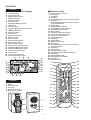
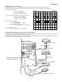
■ Multi-function LCD display
■ Remote control
01.
02.
03.
04.
05.
06.
07.
08.
09.
10.
11.
12.
13.
14.
15.
16.
17.
18.
19.
20.
21.
22.
23.
24.
25.
26.
01.
02.
03.
04.
05.
06.
07.
Function Indicator
Timer Play Indicator
FM Stereo Mode Indicator
FM Stereo Indicator
Extra Bass Indicator
Record Indicator
CD/CD-R/CD-RW Play Indicator
CD Indicators
Cassette Indicator
CD CD-R High Speed Record Indicator
CD-R/CD-RW Indicator
Auto Mark Indicator
Erase Indicator
Digital Source Indicator
Finalize Indicator
Memory Indicator
CD All Disc Play Indicator
Random Play Indicator
Music Schedule Indicator
Synchronized Recording Indicator
CD/CD-R/CD-RW Repeat Indicator
CD/CD-R/CD-RW Pause Indicator
Tape Reverse Mode Indicator
Sleep Indicator
Timer Recording Indicator
Character Information Display
8
1
2
3
4
5
6
7
9
10
11
08.
09.
10.
11.
12.
13.
14.
15.
16.
17.
18.
19.
20.
21.
22.
23.
24.
25.
26.
27.
28.
29.
30.
12
13
14
15
16
17
18
19
20 22 24 26
21 23 25
CP-RW5000
1.
2.
3.
4.
5.
6.
Tweeter
Woofer
Bass Reflex Duct
Subwoofer
Subwoofer Terminals
Main Speaker Terminals
1
4
2
5
3
6
–4–
Remote Control Transmitter
Power Button
CD-R Button
CD Button
CD/CD-R/CD-RW Play or Pause/Tape Play Button
Enter Button
CD/CD-R/CD-RW Fast Reverse, Tape Fast Wind
or Preset Down Button
Dimmer Button
CD-R/CD-RW Record Button
CD-R/CD-RW Record Mode Button
CD-R/CD-RW Finalize Button
Memory Button
Tape Reverse Mode Select Button
Control Panel Open/Close Button
Volume Up or Down Buttons
Tuner (Band) Button
Tape Button
Auxiliary Button
CD Direct Play Buttons
Menu Button
CD/CD-R/CD-RW Fast Forward, Tape Fast Wind
or Preset Up Button
Stop Button
Display Button
Tape Record Pause Button
CD/CD-R/CD-RW Play Mode Select Button
Clear Button
FM Stereo Mode Button
Equalizer Mode Select Button
Time Button
Extra Bass Button
1
16
2
17
3
18
4
19
5
20
6
21
7
22
8
23
9
24
10
25
11
26
12
27
13
28
14
29
15
30
CD-RW5000
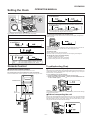
Setting the Clock
OPERATION MANUAL
6
Turn the jog dial to adjust the hour and within 2 minutes, press
the ENTER button.
● When the 12-hour display is selected, “AM” will change automatically to “PM”.
7
Turn the jog dial to adjust the minutes and within 2 minutes, press
the ENTER button.
● The hour will not advance even if minutes advance from “59” to “00”.
● The clock starts from “0” second. (Seconds are not displayed.)
The time display will disappear after a few seconds.
In this example, the clock is set for the 12-hour (AM12:00) display.
1
2
3
4
Press the POWER button to turn the power on.
To confirm the time display in the stand-by mode:
Press the DISPLAY button on the remote control. The time display will appear for
about 3 seconds.
Press the MENU button.
Turn the jog dial to select “CLOCK” and within 10 seconds, press
the ENTER button.
Within 2 minutes, press the ENTER button again.
Note:
“CLOCK” will appear or time will flash at the push of the DISPLAY button when the AC
power supply is restored after a power failure or after unplugging the unit.
Reset the clock as follows.
To reset the clock:
5
Turn the jog dial to select the 12-hour or 24-hour display and
within 2 minutes, press the ENTER button.
Perform “Setting the Clock” from the beginning.
At this time, step 5 (for selecting the 12-hour or 24-hour display) will be skipped.
To change the 12-hour or 24-hour display:
1. Clear all the programmed contents.
[Refer to “If trouble occurs (reset)” for details.]
2. Perform “Setting the Clock” from the beginning.
“AM 12:00”→ The 12-hour display will appear. (AM 12:00 - PM 11:59)
“AM 0:00” → The 12-hour display will appear. (AM 0:00 - PM 11:59)
“0:00”
→ The 24-hour display will appear. (0:00 - 23:59)
Remote Control
Troubleshooting Chart
■ Test of the remote control
■ If trouble occurs (reset)
Face the remote control directly to the remote sensor on the unit.
The remote control can be used within the range shown below:
Press the POWER button. Does the power turn on? Now, you can enjoy the music.
When this product is subjected to strong external interference (mechanical shock, excessive static electricity, abnormal supply voltage due to lightning, etc.) or if it is operated incorrectly, it may malfunction.
If such a problem occurs, do the following:
1. Press the POWER button to enter the power stand-by mode.
2. While pressing down the VOLUME
button, press the POWER button until “ALL CLEAR” appears.
Remote sensor
8" - 20'
(0.2 m - 6 m)
Caution:
This operation will erase all data stored in memory including clock and timer settings,
and tuner and CD presets.
■ Before transporting the unit
Remove the CD-R/CD-RW disc and all CDs from the unit. Your unit checks whether
there are any discs inside the unit when the tray is closed. “CDR NO DISC” and “CD
NO DISC” appear if no disc is left. Then, set the unit to the power stand-by mode.
Carrying the unit with discs left inside can damage it.
and
–5–
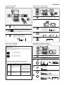
CD-RW5000
1
Accessories
Accesorios
3
System Connections
Conexiones del sistema
FM antenna
Antena de FM
AM loop antenna
Antena de cuadro de AM
Remote control × 1
Controlador remoto × 1
AM loop antenna × 1
Antena de cuadro de AM × 1
2
Left speaker
Altavoz izquierdo
FM antenna × 1
Antena de FM × 1
Blue
Azul
Red
Rojo
Black
Negro
Black
Negro
Speaker wire for
MAIN terminals × 2
Cable del altavoz para
los terminales MAIN × 2
CD-R × 1
CD-R × 1
Right speaker
Altavoz derecho
Blue
Azul
Red
Rojo
Black
Negro
Speaker wire for
SUBWOOFER terminals × 2
Cable del altavoz para los
terminales SUBWOOFER × 2
Left speaker
Altavoz izquierdo
Battery Installation of the Remote Control
Instalación de las pilas del controlador remoto
Use 2 “AA” size batteries (UM/SUM-3, R6, HP-7 or similar).
Use dos pilas del tamaño“AA” (UM/SUM-3, R6, HP-7 o equivalentes).
1
Open the
battery cover.
Abra la cubierta
de las pilas.
2
AC outlet
(AC 120 V, 60 Hz)
A un tomacorriente de
CA (120 V de CA, 60 Hz)
Batteries are not included.
Las pilas no están incluidas.
Insert the batteries
as shown.
Inserte las pilas
como se muestra.
3 Close the cover.
Cierre la cubierta
de las pilas.
Right speaker
Altavoz derecho
Turning on Your System
Conexión de la alimentación de su sistema
4
The first time the unit is plugged, the
unit will enter the demonstration
mode. You will see words scroll.
1
Cuando se enchufe por primera vez el
aparato, se establecerá en el modo de
demostración. Verá un desplazamiento
de palabras.
Listening to a CD (CDs)
Audición de un disco CD (CDs)
Press the DEMO
button to cancel
the demonstration mode.
Pulse el botón
DEMO para
cancelar el modo
de demostración.
2
Press the POWER
button to turn the
power on.
Pulse el botón POWER
para conectar la
alimentación.
Listening to a Cassette Tape
Audición de una cinta cassette
DISC 1
Press the CD button.
1
2
Pulse el botón CD.
DISC 1
Press the DISC 1
button to open the disc tray 1.
Pulse el botón DISC 1 para abrir la bandeja del disco 1.
Press the TAPE button.
2
Open the cassette door by pushing the area marked “PUSH EJECT
Pulse el botón TAPE.
Abra la puerta del cassette pulsando la parte marcada “PUSH EJECT
Place the CD on the disc tray 1, label side up.
3
”.
”.
PUSH EJECT
Coloque el disco compacto en la bandeja del disco 1, con el lado de la etiqueta
hacia arriba.
5” (12 cm)
3” (8 cm)
5” (12 cm)
4
1
DISC 1
3” (8 cm)
3
Load the cassette into the compartment with side A facing you.
Cargue el cassette en el compartimiento con la cara A encarada hacia usted.
4
Press the REV. MODE button to choose one side or both side.
Pulse el botón REV. MODE para seleccionar una cara o ambas caras.
Press the DISC 1
button to close the disc tray 1.
para cerrar la bandeja del disco 1.
Pulse el botón DISC 1
Means “disc inside ”
Significa “disco dentro”
Total number of tracks
Número total de pistas
Total playing time
Tiempo total de reproducción
5
You can place discs on the trays 2 - 6 by following the steps 2 - 4.
Podrá colocar discos en las bandejas 2 - 6 según los pasos 2 - 4.
Press the
6
Pulse el botón
... To listen to both sides.
Para escuchar ambas caras.
... For endless repeat play of both sides.
Para repetir indefinidamente ambas caras.
... To listen to one side.
Para escuchar una cara.
button to start playback.
para iniciar la reproducción.
5
–6–
Press the
Pulse el botón
button to listen to side A, or the
button for side B.
para escuchar la cara A, o el botón
para la cara B.
CD-RW5000
Listening to the Radio
Audición de la radio
Recording to a Cassette Tape
Grabación en una cinta cassette
1
Press the CD button and load the desired disc.
2
Load a cassette into the compartment with side A facing you.
Cargue un cassette en el compartimiento con la cara A encarada hacia usted.
3
Press the REV. MODE button to choose one side or both side.
Pulse el botón REV. MODE para seleccionar de una cara o ambas caras.
Pulse el botón CD y cargue el disco deseado.
Press the TUNER (BAND) button to select the desired frequency band (FM
or AM).
1
Pulse el botón TUNER (BAND) para seleccionar la banda de frecuencia deseada
(FM o AM).
Press the TUNING (
2
or
) button to tune into the desired station.
... To record on both sides.
Para grabar en ambas caras.
... To record on only one side.
Para grabar sólo en una cara.
When the TUNING button is pressed for more than 0.5 seconds, scanning will start
automatically and the tuner will stop at the first receivable broadcast station.
Pulse el botón TUNING (
o
) para sintonizar la emisora deseada.
Cuando se pulse el botón TUNING durante más de 0,5 segundos, la exploración se
iniciará automáticamente y el sintonizador se parará en la primera emisora difusora que
pueda recibirse.
4
Press the TAPE REC button repeatedly to switch to the side you record
on.
Pulse repetidamente el botón TAPE REC para cambiar a la cara que grabe.
5
Press one of the DISC 1 - DISC 6 buttons to start recording.
Pulse uno de los botones DISC-1 a DISC 6 para iniciar la grabación.
To receive an FM stereo transmission, press the ST-MODE button on the
remote control. The “ST” indicator lights up.
3
“
” will appear when an FM broadcast is in stereo.
Para recibir la transmisión de FM en estéreo, pulse el botón ST-MODE del
controlador remoto. Se enciende el indicador “ST”.
“
” aparecerá cuando una difusión de FM sea en estéreo.
Recording to a CD-R or a CD-RW
Grabación en un CD-R o en un CD-RW
What is CD-R or CD-RW?
¿Qué es CD-R o CD-RW?
■ Playable discs
Discos que pueden reproducirse
This player is compatible with CD-R discs, CD-RW discs, and audio CDs with either mark below.
Este reproductor es compatible con discos CD-R, discos CD-RW, y discos compactos de audio con
cualquiera de las dos marcas de abajo.
CD-R:
CD-R:
Compact Disc-Recordable
Disco compacto grabable
CD-RW: Compact Disc-ReWritable
CD-RW: Disco compacto regrabable
1
Press the CD button and load the desired CD(s).
Pulse el botón CD y cargue el disco deseado (los discos deseados).
2
Load the CD-R or CD-RW disc.
Cargue el disco CD-R o CD-RW.
3
Press the REC MODE button and select the desired CD using the jog dial.
Within 10 seconds, press the ENTER button.
Pulse el botón REC MODE y seleccione el disco compacto deseado empleando el
mando de lanzadera. Antes de transcurrir 10 segundos, pulse el botón ENTER.
■ Differences between the CD-R disc and the CD-RW disc
Diferencias entre el disco CD-R y el disco CD-RW
CD-R
CD-RW
Playback
Can be played on a standard CD player Cannot be played on a standard CD
player.
Reproducción when it is finalized after recording.
Se puede reproducir en un reproductor de If it is finalized after recording, it can
CD estándar cuando se finaliza después be played only on a CD-RW compatible
player.
de la grabación.
In steps 4 - 6, operate within 5 seconds. Otherwise, the system will go to the next step automatically.
En los pasos 4 – 6, opere antes de 5 segundos. De lo contrario, el sistema pasará al paso siguiente automáticamente.
4
No se puede reproducir en un reproductor
de CD estándar. Si se finaliza después de
la grabación, se puede reproducir sólo en
un reproductor compatible con discos CDRW.
Erasing
Erasing is impossible.
Borrado
El borrado es imposible.
Press the CD CDR button.
Pulse el botón CD CDR.
5
Select “AUTO” using the jog dial to finalize the disc. Then press the ENTER button.
Seleccione “AUTO” empleando el mando de lanzadera para finalizar el disco.
Entonces, pulse el botón ENTER.
6
Select “HIGH” using the jog dial to record at high speed. Then press the
ENTER button to start recording.
Seleccione “HIGH” empleando el mando de lanzadera para grabar a alta
velocidad. Luego, pulse el botón ENTER para iniciar la grabación.
Recorded tracks can be deleted.
A finalized disc can be restored.
Se pueden borrar pistas grabadas.
Se puede restaurar un disco finalizado.
–7–
CD-RW5000
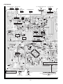
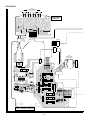
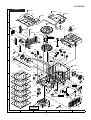
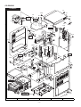
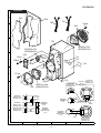
DISASSEMBLY
CD-RW5000
Caution on Disassembly
Follow the below-mentioned notes when disassembling
the unit and reassembling it, to keep it safe and ensure
excellent performance:
1. Take cassette tape and compact disc out of the unit.
2. Be sure to remove the power supply plug from the wall
outlet before starting to disassemble the unit.
3. Take off nylon bands or wire holders where they need to
be removed when disassembling the unit. After servicing
the unit, be sure to rearrange the leads where they were
before disassembling.
4. Take sufficient care on static electricity of integrated
circuits and other circuits when servicing.
Top Cabinet
(A1)x2
ø3x16mm
Front Panel
(A1)x2
ø3x16mm
(A1)x1
ø3x10mm
Side Panel
(Left)
(B1)x4
ø3x10mm
CD-RW5000
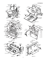
PROCEDURE
FIGURE
1
Top Cabinet
1. Screw ................ (A1) x5
8-1
2
Side Panel(Left/Right) 1. Screw ................ (B1) x8
8-1
3
Rear Panel
1. Screw ................ (C1) x3
2. Screw ................ (C2) x10
8-2
4
Front Panel
1. Flat Cable .......... (D1) x1
2. Screw ................ (D2) x4
3. Socket ............... (D3) x6
8-2
5
Sub Trans PWB
1. Screw ................ (E1) x3
2. Socket ............... (E2) x5
8-2
6
Main PWB
1. Flat Cable .......... (F1) x1
2. Screw ................ (F2) x2
3. Screw ................ (F3) x1
4. Socket ............... (F4) x3
5. Flat Cable .......... (F5) x2
8-2
STEP
REMOVAL
(B1)x4
ø3x10mm
Rear Panel
Side Panel(Right)
Figure 8-1
(D1)x1
Power PWB
(F3)x1
ø3x8mm
Tape Mechanism PWB
(D3)x2
Speaker
PWB
(C1)x1
ø3x10mm
Front Panel
Main PWB
7
CD-R Unit
1. Socket ............... (G1) x1
2. Screw ................ (G2) x4
9-1
8
Power PWB/
Speaker PWB
1. Socket ............... (H1) x1
2. Screw ................ (H2) x2
9-1
9
Tape Mechanism
1. Open the cassette holder
2. Screw ................ (J1) x4
9-2
10
CD Switch PWB/
CD-R PWB
1. Socket ............... (K1) x1
2. Screw ................ (K2) x7
3. Hook .................. (K3) x2
9-2
11
Switch PWB
1. Screw ................ (L1) x1
9-2
12
Headphones PWB
1. Screw ................ (M1) x1
2. Bracket .............. (M2) x1
9-2
13
CD Changer door
panel/
Control Panel
1. Screw ................ (P1) x3
2. Screw ................ (P2) x2
9-2
14
Motor PWB
1. Solder ................ (Q1) x2
9-2
15
CD Changer door
panel
1. Screw ................ (R1) x4
9-3
16
Control Panel
1. Screw ................ (S1) x6
9-3
17
Control PWB
1. Screw ................ (T1) x5
2. Socket ............... (T2) x1
9-4
18
Jog PWB
1. Screw ................ (U1) x5
9-4
19
LED B PWB
1. Screw ................ (V1) x3
9-4
20
Cassette holder
Cover
1. Open the cassette holder Cover
2. Screw ................ (W1) x4
3. Display Panel .... (W2) x1
4. Hook .................. (W3) x4
9-5
21
Display PWB/
LED A PWB
1. Screw ................ (X1) x4
2. Hook .................. (X2) x2
9-6
(F4)x1
(C1)x2
ø3x10mm
(F2)x2
ø3x10mm
CD PWB
(F1)x1
Rear
Panel
(D2)x2
ø3x8mm
(C2)x10
ø3x10mm
Power PWB
Speaker
PWB
Main PWB
(D3)x4
(E2)x3
(D2)x1
ø3x8mm
(F4)x2
Sub Trans
PWB
(F5)x2
(E2)x2
CD-R Unit
(D2)x1
ø3x8mm
(E1)x3
ø3x8mm
–8–
Figure 8-2
CD-RW5000
Control PWB
Control Panel B
(H2)x1
ø3x10mm
Speaker
PWB
(H2)x1
ø3x10mm
Power PWB
CD-R Unit
(G2)x2
ø3x8mm
Jog PWB
(T1)x5
ø2.6x10mm
(V1)x2
ø2.6x10mm
(G1)x1
(H1)x1
(V1)x1
ø2.6x10mm
Main
Chassis
(T2)x1
(U1)x5
ø2.6x10mm
(G2)x2
ø3x8mm
CD Changer
Block
LED B PWB
LED Holder
Figure 9-1
Front Panel
Cassette
Holder
Open
Control Panel A
(J1)x4
ø3x10mm
Figure 9-4
Tape
Mechanism
CD-R PWB
(K2)x1
ø3x10mm
(W3)x4
CD Switch
PWB
(K3)x1
Front Panel
Open
Cassette
Holder Cover
(K3)x1
(K1)x1
(W1)x4
ø2.6x12mm
(K2)x6
ø3x10mm
(P2)x1
ø3x20mm
CD Changer
Door Panel
(Q1)x2
Motor
PWB
(W2)x1
Switch PWB
(P1)x3
ø3x10mm
(P2)x1
ø3x20mm
Headphones
PWB
(L1)x1
ø2.6x10mm
(M1)x1 (M2)x1
ø3x10mm
Figure 9-2
CD Changer
Door Panel
Figure 9-5
Cassette
Holder Cover
(S1)x2
ø2.6x12mm
(R1)x1
ø2.6x10mm
(R1)x2
ø2.6x10mm
LED A
PWB
(X2)x1
(S1)x2
ø2.6x12mm
Display
PWB
(X1)x4
ø3x14mm
(S1)x2
ø2.6x12mm
Control Panel
(X2)x1
Figure 9-3
(R1)x1
ø2.6x10mm
Figure 9-6
–9–
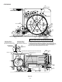
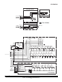
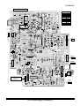
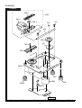
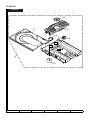
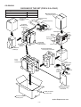
CD-RW5000
CP-RW5000
CD-RW5000 (CD CHANGER MECHANISM UNIT)
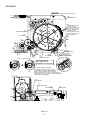
STEP
REMOVAL
PROCEDURE
FIGURE
STEP
8-1
1
1
Top Cabinet
2
Side Panel(Left/Right) 1. Screw ................ (B1) x8
8-1
3
Rear Panel
1. Screw ................ (C1) x3
2. Screw ................ (C2) x10
8-2
4
Front Panel
1. Flat Cable .......... (D1) x1
2. Screw ................ (D2) x4
3. Socket ............... (D3) x6
8-2
5
CD Changer
Mechanism
1. Flat Cable .......... (Y1) x1
2. Screw ................ (Y2) x2
3. Screw ................ (Y3) x5
10-1
6
CD PWB
(Note)
1. Screw ................ (Z1) x4
2. Socket ............... (Z2) x4
3. Flat Wire ............ (Z3) x2
10-2
CD Mechanism
1. Screw ................ (ZZ1) x4
10-2
7
1. Screw ................ (A1) x5
PROCEDURE
REMOVAL
Woofer/Tweeter/
Sub Woofer
FIGURE
1. Net ................... (A1) x1
2. Front Panel ..... (A2) x1
3. Screw .............. (A3) x4
4. Ring ................. (A4) x1
5. Catching holder (A5) x2
6. Screw .............. (A6) x2
7. Cover ............... (A7) x1
8. Screw .............. (A8) x2
9. Screw .............. (A9) x4
10. Cover ............. (A10) x10
10-3
10-4
10-5
(A1)x1
Note:
After removing the connector for the optical pickup from the
connector, wrap the conductive aluminium foil around the
front end of connector remove to protect the optical pickup
from electrostatic damage.
(A2)x1
Driver should
be pried away
from Speaker Box.
Slide it in the direction of the arrow
after removing the screw (Y2).
CD Changer
Mechanism
Front Side
Screw Driver
Speaker Box
Bottom Side
Figure 10-3
Speaker Box
(Y2)x1
ø3x10mm
(A7)x1
CD PWB
Bottom Side
(Y3)x3
ø3x10mm
(A5)x2
(A6)x2
ø3x10mm
(Y2)x1
ø3x10mm
(A8)x2
ø3x10mm
(Y1)x1
(Y3)x2
ø3x10mm
Main Chassis
Figure 10-1
(Z1)x4
ø3x10mm
(Z2)x2
(A3)x4
ø4x16mm
(A4)x1
(Z3)x1
(Z2)x1
Tweeter
Woofer
Figure 10-4
(Z3)x1
Speaker Box
CD PWB
(ZZ1)x4
ø2.6x10mm
Top Side
Sub Woofer
(Z2)x1
CD Changer
Mechanism
(A10)x1
(A9)x4
ø4x20mm
CD Mechanism
Rear Side
Figure 10-2
Figure 10-5
– 10 –
CD-RW5000
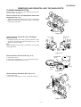
REMOVING AND REINSTALLING THE MAIN PARTS
TAPE MECHANISM SECTION
Perform steps 1 to 4 and 8 of the disassembly method to
remove the tape mechanism.
How to remove the record/playback and erase
heads (See Fig. 11-1)
Erase
Head
1. When you remove the screws (A1) x 2 pcs., the recording/
playback head and three-dimensional head of the erasing
head can be removesd.
Record/
Playback
Head
(A1)x2
Ø2 x 6mm
Figure 11-1
How to remove the pinch roller (Left/Right)
(See Fig. 11-2)
(Left)
(Right)
Pinch
Roller
Pawl
1. Carefully bend the pinch roller pawl in the direction of the
arrow <A>, and remove the pinch roller (B1) x1 pc., in the
direction of the arrow <B>.
Note:
When installing the pinch roller, pay attention to the spring
mounting position.
Pull
<A>
Pinch
Roller
Pawl
Pinch
Pull Roller Pull <B>
(B1)x1
<B>
Pull
<A>
Figure 11-2
How to remove the belt (See Fig. 11-3)
FF/REW Belt
(C2)x1
1. Remove the motor.
2. Remove the main belt (C1) x 1 pc., from the motor side.
3. Remove the FF/REW belt (C2) x 1 pc.
Motor
Main Belt
(C1)x1
Figure 11-3
How to remove the motor (See Fig. 11-4)
Motor
1. Remove the belt.
2. Remove the screws (D1) x 2 pcs., to remove the motor.
(D1)x2
Ø 2.6 x 5mm
Figure 11-4
– 11 –
CD-RW5000
FRONT PANEL SECTION
Perform steps 1 to 4 of the disassembly method to remove the
front panel.
How to remove the control panel motor
(See Fig. 12-1)
(E1)x1
ø2.6x10mm
CD Changer
Door Panel
CD Changer
Door Panel
1. Remove the control panel.
2. Remove the screws (E1) x 6 pcs., to remove the CD changer
door panel.
3. Remove the screws (F1) x 2 pcs., to remove the control
panel motor.
(F1)x2
ø2x5mm
Gear Box A
Control
Panel
Motor
(E1)x2
ø2.6x10mm
Motor PWB
Gear Box B (E1)x3
ø2.6x10mm
Control Panel
Figure 12-1
CD MECHANISM SECTION
Perform steps 1 to 7 of the disassembly method to remove the
CD mechanism. (See page 10.)
How to Remove the pickup (See Fig. 12-2.)
Stop Washer
(A1) x1
(A3) x1
ø2.6 x6mm
1. Remove the screws (A1)x 2 pcs., to remove shaft (A2)x 1
pc.
2. Remove stop washer (A3)x 1 pc., to remove gear (A4)x 1 pc.
3. Remove the pickup.
(A1) x1
ø2.6 x6mm
Pickup
CD
Mechanism
Note:
After removing the connector for the optical pickup from the
connector, wrap the conductive aluminium foil around the
front end of connector remove to protect the optical pickup
from electrostatic damage.
Shaft
(A2) x1
Gear
(A4) x1
Figure 12-2
CD CHANGER MECHANISM SECTION
Perform steps 1 to 5 of the disassembly method to remove the
CD changer mechanism. (See page 10.)
How to Remove the tray motor/main cam motor
(See Fig. 12-3.)
1. Remove the screws (B1)x 4 pcs., to remove the CD PWB.
2. Remove the (1)front top plate, (2)changer box, left/right and
(3)disc trays 1~6. After that, disassemble as shown in the
figure.
3. Remove the screws (B2)x 4 pcs.
4. Remove the tray motor and main cam motor.
Note:
The parts of (1), (2) and (3) correspond to the drawing Nos.
117, 102, 103 and 108 to 113 of the CD change mechanism
disassembly drawing.
Remove the screws of 117, 102 and 103, and the parts of (1),
(2) and (3) will be ready for removal and the screws of the tray
motor and main cam motor will be visible.
CD Changer Mechanism
(2)Changer Box,
Right
(1)Front Top Plate
(2)Changer Box,
Left
(3)Disc Tray,1~6
(B2)x4
ø2.6x4mm
CD PWB
(B1)x4
ø3x10mm
Main Cam Motor
Tray Motor
Figure 12-3
– 12 –
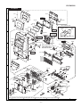
CD-RW5000
CD CHANGER MECHANISM MAIN BASE PARTS ASSEMBLING/ADJUSTING
PROCEDURE
Work content
Applied part No.
1. Motor assembly (x 2) mounting (screw x 4)
Assembly fig. No.
101/129
2. MT idle gear mounting (screw x 1)
125
Fig.14
3. MT system gear assembly
123/124/126/127
Fig.14
4. STB/tray drive system gear and others assembling/
mounting (screw x 3)
137/138/145/146 (153)/147/148
Fig.14
5. Tray big gear assembly
131
Fig.14
6. T.M SW PWB mounting (screw x 3)
7. STB holder assembling
Remarks
Fig.14
Gear positioning
Fig.15
103
Fig.14
8. STB drive gear L/R assembly mounting (screw x 2)
111 (110)/112 (110)
Fig.14
9. Tray joint gear R/tray drive gear R assembling
134/136
Fig.15
Gear positioning
10. Tray gear A/B assembling
132/133
Fig.15
Gear positioning
11. Lift gear B/C assembling
143/144
Fig.16
Gear positioning
12. MT idler gear F assembling, mode big gear
mounting (screw x 1)
128/142
Fig.16
13. Change box R mounting (screw x 4)
104
Fig.16
14. Lift gear A assembling
142
Fig.16
15. Change box L assembly mounting (screw x 4)
102/130/135
Fig.17
16. Lift cam assembling (shaft inserting)
144
Fig.17
Gear positioning
Fig.18
Check/adjustment
17. STB holder height adjusting
18. Top plate F/disc OB LEV. mounting (screw x 6)
180
19. Trays 1 - 6 assembling
191/192/193/194/195/196
Gear positioning
Fig.18
20. Top plate R mounting (screw x 6)
Fig.19
-
CD CHANGER MECHANISM PARTS LIST
Part name
No.
No.
Part name
101
MAIN BASE
140
LIFT CAM
102
CHANGE BOX L
141
MODE BIG GEAR
103
STB HOLDER
142
LIFT GEAR A
104
CHANGE BOX R
143
LIFT GEAR B
144
LIFT GEAR C
110
STB DRIVE GEAR A
145
STB GEAR A
111
STB DRIVE GEAR L
146
STB GEAR B
112
STB DRIVE GEAR R
147
STB GEAR C
120
STABILIZER FH
148
STB GEAR D
123
MT IDLER GEAR A
150
LIFT LEVER
124
MT IDLER GEAR B
151
TRAY LOCK LEVER
125
MT IDLER GEAR C
152
DISC OB LEVER
126
MT IDLER GEAR D
153
STB GEAR ANG.
127
MT IDLER GEAR E
128
MT IDLER GEAR F
180
TOP PLATE F
129
MOTOR GEAR
181
TOP PLATE R
130
TRAY DRIVE GEAR F
131
TRAY BIG GEAR
191
TRAY 1
132
TRAY GEAR A
192
TRAY 2
133
TRAY GEAR B
193
TRAY 3
TRAY DRIVE GEAR R
194
TRAY 4
135
TRAY JOINT GEAR F
195
TRAY 5
136
TRAY JOINT GEAR R
196
TRAY 6
137
TRAY GEAR C
138
TRAY IDLER GEAR
134
– 13 –
CD-RW5000
112
STB DRIVE GEAR R
(ASSY)
148
STB GEAR D
103
STB HOLDER
101
MAIN BASE
124
129
129
123
126
110
STB DRIVE GEAR A
123
Mark position
125
127
145
STB GEAR A
153
STB GEAR ANG.
146
STB GEAR B
147
STB GEAR C
110
STB DRIVE GEAR A
111
STB DRIVE GEAR L
(ASSY)
137
138
TRAY GEAR C
TRAY IDLER GEAR
131
TRAY BIG GEAR
After assembling TRAY BIG GEAR, turn it in the arrow direction.
TRAY BIG GEAR ASSEMBLING POSITION
111(/112) (110)
STB DRIVE GEAR L(/R)
(ASSY)
146
STB GEAR B
147
STB GEAR C
153
STB GEAR ANG.
145
STB GEAR A
137
138
TRAY GEAR C
TRAY IDLER GEAR
Figure 14
– 14 –
131
TRAY BIG GEAR
CD-RW5000
124
129
129
123
126
123
125
127
Mark position
* This position becomes the
reference (stock) position
of the tray.
145
132
TRAY GEAR A
146
147
These holes must align.
110
111
Direct the recess part
(trapezoidal side) of the axis
135 in this direction.
138
137
131
134
136 TRAY DRIVE GEAR R
M T SW PWB
TRAY JOINT GEAR R
Scale: 2 magnifications
*2
133
TRAY
GEAR B
Scale: 2 magnifications
It must not rotate in contact
with the peripheral (hatched)
part of 131.
132
TRAY BIG GEAR SET POSITION
133
These holes must align.
*1: To position the axis part of 136, engage it with 138.
After assembling 132,
assemble 133.
*1 *2: When it is aligned as described in *1, the hatched part
(low gear-height part of gear) will be positioned in this position.
Note: After positioning the tray big gear in the set position, engage these gears.
134
TRAY DRIVE GEAR R
136
TRAY JOINT GEAR R
133
TRAY GEAR B
Figure 15
– 15 –
132
TRAY GEAR A
CD-RW5000
Mark position
(Assemble the mode big gear in this position.)
104
CHANGE BOX R
,,,,,,,,,,,,,,,,
,,,,,,,,,,,,,,,,
,,,,,,,,,,,,,,,,
,,,,,,,,,,,,,,,,
,,,,,,,,,,,,,,,,
,,,,,,,,,,,,,,,,
,,,,,,,,,,,,,,,,
,,,,,,,,,,,,,,,,
,,,,,,,,,,,,,,,,
,,,,,,,,,,,,,,,,
,,,,,,,,,,,,,,,,
,,,,,,,,,,,,,,,,
,,,,,,,,,,,,,,,,
,,,,,,,,,,,,,,,,
,,,,,,,,,,,,,,,,
,,,,,,,,,,,,,,,,
,,,,,,,,,,,,,,,,
,,,,,,,,,,,,,,,,
,,,,,,,,,,,,,,,,
,,,,,,,,,,,,,,,,
,,,,,,,,,,,,,,,,
,,,,,,,,,,,,,,,,
,,,,,,,,,,,,,,,,
,,,,,,,,,,,,,,,,
,,,,,,,,,,,,,,,,
,,,,,,,,,,,,,,,,
128
MT IDLER GEAR F
142
LIFT GEAR A
Note
To assemble the mode
big gear, incline it,
bring it into contact with
the circumference and
put the center hole into
position since the
hatched part of the main
base is overlapped with
the circumference.
132
133
145
153
146
110
147
144
LIFT GEAR C
137
138
111
143
LIFT GEAR B
134
136
141
MODE BIG GEAR
Direct the short tooth
toward the center.
Scale: 2 magnifications
Scale: 2 magnifications
MODE BIG GEAR
LIFT GEAR A/B/C
ASSEMBLING POSITION
(A)
(B)
<Assembling method of lift gear>
After setting up the mode big gear in the
shown position, engage it with the STB gear A
(gear on the lower side) at the position (A),
and assemble them, turning it in the arrow direction
into the position (B). (The short tooth directs toward the
center of the mode big gear.)
142
LIFT GEAR A
141
MODE BIG GEAR
143
LIFT GEAR B
Figure 16
– 16 –
144
LIFT GEAR C
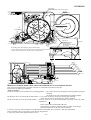
CD-RW5000
37°
Mark position
128
142
LIFT GEAR A
132
133
145
130
TRAY DRIVE GEAR F
146
110
147
111
141
143
TRAY JOINT GEAR F
(CHANGE BOX L ASS'Y) ASSEMBLING POSITION
LIFT CAM
144
140
LIFT CAM
Scale: 2 magnifications
Assembling procedure
1. Turn the mode big gear approx. 37 degrees in the arrow direction.
2. Assemble the change box L ass'y.
Note: At this time, the tray joint gear F must be located in the position shown in figure.
Moreover, the gear must be engaged securely.
3. After assembly, return the mode big gear to the initial position.
4. Assemble the lift cam.
Note: At this time, the lift cam (No.140) must be located in the position shown in figure 17.
102
CHANGE BOX L
Direct the recess part (trapezoidal side)
of the axis 135 in this direction.
135
TRAY JOINT GEAR F
*2
130
TRAY DRIVE GEAR F
135
TRAY JOINT GEAR F
*1: To position the axis part
of 135, engage it with 133.
*2: When it is aligned as
described in *1, the hatched part
140
(low gear-height part of gear)
will be positioned as shown.
LIFT CAM
Since this gear engagement is not
visually checked, verify that it does
not float when the gear box L is installed.
*1
Scale: 2 magnifications
During assembly, make the
O part visible in this direction.
Note: Among 4 ribs on the
circumference, one rib alone
is provided with O.
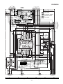
130
135 TRAY DRIVE GEAR F
TRAY JOINT GEAR F
Figure 17
– 17 –
CD-RW5000
180
TOP PLATE F
37°
Mark position
142
LIFT GEAR A
132
133
145
130
146
110
147
135
111
141
143
140
144
STB HOLDER HEIGHT ADJUSTING METHOD
When the height of
STB holder is high,
(Decrease the clearance.)
When the height of
STB holder is low,
(Increase the clearance.)
Bend this part.
240
OS LEVER
Adjusting procedure
1. Turn the mode big gear approx. 37 degrees in the arrow direction.
2. Viewing from the front side of the mechanism, verify that the guide ribs
(CHANGE BOX L/R and STB HOLDER)of tray are as tall as each other.
3. If they are not, bend the lever for adjustment. (Refer to the details.)
Note: Also apply the same adjustment on the R side.
,,
,,
,,
,,
,,
,,
,,
Bend this part to adjust the height of the STB holder.
Scale: 2 magnifications
Details
180
TOP PLATE F
140
Height of the rib
130
135
Figure 18
– 18 –
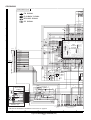
CD-RW5000
Mark position
Be sure to assemble the tray into this position.
191~196
TRAY1~TRAY6
Insert it along the guide of
the change box.
142
LIFT GEAR A
132
133
145
,,,,
,,,,
,,,,
146
110
147
130
TRAY No.1~6
111
141
143
140
144
Tray installing method: (After adjusting the height of the STB holder)
Rear side
Rear surface: Stamped.
Note: During insertion,
Do not accidentally rearrange
tray numbers.
135
,,
,,
,,
1. Turn the mode big gear to the mark position to lower the STB holder to the bottom area.
2. From the front side, install the tray. (Securely insert it to the lock position.)
140
TRAY 6
TRAY 5
TRAY 4
TRAY 3
TRAY 2
TRAY 1
130
135
Figure 19
Measure to be taken when a disc cannot be removed due to a mechanism trouble
First, remove the mechanism unit section from the set, and check for the state of the disc.
(Remove the top plate R if necessary.)
<State of the disc>
(1) When the disc is in the normal PLAY (chucking) position -> Try to eject the disc by turning the mode big gear/tray big gear
manually.
* At this time, be sure to adjust the tray's position (height).
(2) When the disc is in the normal STOCK position -> Try to eject the disc by turning the tray big gear manually.
* At this time, be sure to adjust the tray's position (height).
(3) When the disc is not in the normal position -> The tray or disc is not in the normal position. (The tray or disc may catch
somewhere.)
Remove the TOP PLATE F/DISC OB lever.
Unlock the tray lock lever and pull out the tray which is not caught.
Move the caught tray or disc and remove the disc.
In case of (1) and (2), the mechanism is normal (defective circuit parts, etc.). However, it may stop somewhere.
This is the reason why you should try to turn the tray big gear first.
In case of (3), either of the big gears does not turn.
– 19 –
CD-RW5000
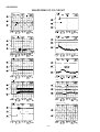
ADJUSTMENT
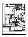
MECHANISM SECTION
MAIN PWB
• Driving Force Check
Torque Meter
AM
Tracking
Specified Value
Play: TW-2412
Over 80 g
BF301
Torque Meter
Play: TW-2111
30 to 60 g. cm
Fast forward: TW-2231
60 to 120 g.cm
• Tape Speed
Specified
Value
Speaker
terminal
13
FM IF
12
1
T351
AM IF
R345
CF352
FM
TP301
SO301
ANTENNA
TERMINAL
TAPE MECHANISM
24
IC303
Instrument
Connection
Variable resistor 3,000 ±90 Hz
in motor
MTT-111
FM Band
Coverage fL
FM RF
GND
VR351
T312
L312
60 to 120 g.cm
Adjusting
Point
9
SO301
Rewind: TW-2231
T311
1
AM
BI960
T306
IC301
Specified Value
1
FM Mute
Level
T302
• Torque Check
Test Tape
AM Band
Coverage fL
IC302
Figure 20-2 ADJUSTMENT POINTS
Variable
Resistor
in motor
Tape motor
Extension cable
Type
1.
Part No.
33 Pin extension
flat cable, 500mm
QCNWN6931AFZZ
Figure 20-1 ADJUSTMENT POINT
TUNER SECTION
fL: Low-range frequency
fH: High-range frequency
• AM IF/RF
Signal generator: 400 Hz, 30%, AM modulated
Display
Frequency Frequency
Setting/ Instrument
Adjusting Connection
Parts
T351
*1
AM IF
450 kHz
1,720 kHz
AM Band
Coverage
—
530 kHz
(fL): T306 *2
1.1 ± 0.1 V
AM
Tracking
990 kHz
990 kHz
T302
CNP1
33
1
*1
CD PWB-C
33
1
*1. Input: Antenna
*2. Input: Antenna
Output: Speaker Terminal
Output: TP301
33Pin extension flat cable
QCNWN6931AFZZ
• FM RF
Signal generator: 1 kHz, 75 kHz dev., FM modulated
Test Stage Frequency
Frequency
Display
Setting/ Instrument
Adjusting Connection
Parts
FM Band
Coverage
—
87.50 MHz
(fL): T311 *1
1.3 ± 50mV
FM RF
98.00 MHz
(10~30 dB)
98.0 MHz
L312
*1. Input: Antenna
*2. Input: Antenna
1
33
MAIN PWB-A
1
33
CNP901
*2
Output: TP301
Output: Speaker Terminal
• FM Mute Level (FM ST MODE)
Signal generator: 1 kHz, 40 kHz dev., FM modulated
Frequency
98.00 MHz
(26 dBµV)
Display
98.00 MHz
Adjusting
Parts
VR351*1
Instrument
Connection
Input:SO301
Output: Speaker
Terminal
Figure 20-3
*1. Adjust so that an output signal appears.
– 20 –
CD-RW5000
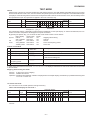
TEST MODE
Outline
While the unit is turned off, press the POWER key while holding down the VOLUME-DOWN and PANEL OP/CL keys to enter
the test mode selection mode. Then, the unit is started, the panel is opened, and the microcomputer's version/destination/span
is displayed. If the following data is entered from the keyboard while in the test mode selection mode, the unit directly enters
the specified test mode. This operation is applied to the main unit's keys only.
Character display
Item
Type
Version•Destination
Auxiliary display
1 2 3 4
V
* •
5 6 7 8 : 9 10 11 12
*
: Span
Number
Auxiliary
display
Note
Left adjust in the first line
Destination
Example: V1. 1_W:_9
In the destination display, a destination code (H/W/U/J) is displayed. For the span display, "9" means 9 kHz/50 kHz, and "10"
means 10/100 kHz. All pictures will disappear except the characters.
By pressing the specific key, you can enter the test mode whose functions are as follows:
Menu display
Shortcut Key
Model
System
INITIAL
CD1 PLAY
ALL
Shipping status setting
SOFT_RESET CD2 PLAY
ALL
Soft rest
CD
CD_TEST
CD1 EJECT
ALL
CD test
Tuner
TUN_PRESET CD4 EJECT
ALL
Tuner test frequency preset
TUNER_TEST CD5 EJECT
ALL
Tuner test
Outline of Test Mode
Name
1
2
3
Shipping status setting
Soft set setting
CD test
4
Tuner test
frequency preset
Tuner preset clear setting
5
>>>>><<<<<
"EDIT Bar"
______
______
flashing on and off
Description
______
Sets up the unit for shipping.
Initializes the unit.
Performs tests such as the CD mechanism test, hardware test,
and constant setting test.
Presets the test frequency.
______
Clears all presets.
In a test which reserves the current mode, "<<<<<<<V<<<<<<<" is displayed and flashes on and off in the EDIT flow section while
in the test mode.
Shipping status setting test mode
Purpose: To Set up the unit for shipping.
Function: Initialize all functions.
Operation: All settings are initialized, "FINISH" is displayed as in the sample display, and data entry is prohibited including data
to turn on or off the unit.
To exit the test mode
The unit returns to the normal operation through reset entry.
Table Character display for test mode 1
Character display
Item
Type
Auxiliary display
Test mode name
Set-Up Complete Function
1 2 3 4 5 6 7 8 : 9 10 11 12
I N I T I A L
F I N I S H
Auxiliary
Note
display
In the destination display, a destination code is displayed. For the span display, "9" means 9 kHz/50 kHz, and "10" means 10/
100 kHz.
– 21 –
CD-RW5000
2. Soft reset
Purpose: To initialize the unit.
Function: To initialize all functions.
Operation: "ALL CLEAR" is displayed, all functions are initialized, and the unit is turned on.
To exit the test mode
When the initialization through soft reset is complete, the unit is turned on.
Table Character display for test mode 2
Character display
Item
Reset operation
display
Type
Auxiliary display
Operation
1 2 3 4
A L L
5 6 7 8 : 9 10 11 12
C L E A
R
Auxiliary
display
Note
3. CD test mode (If this test mode is not activated, refer to CD troubleshooting on page 54.)
In the CD test mode, each step can be performed even if the LID-SW is off. However, if you cannot obtain a focus in step
3 or if other kind of error handling starts, you cannot proceed to the following steps. In error handling, press the POWER key
to exit the test mode, or press the STOP key to prohibit operations other than returning to step 1.
(1) Step 1 mode
In the CD test mode, the following display appears, CD initialization is performed, and you are prompted for data.
Reset operation display / Operation
"CD_TEST"
After lighting up for one second
"T1___________0:00"
The keys you can press here and the resulting operations are as follows:
"POWER" ........... The test mode is turned off, the power is turned off, and the unit is placed in the normal standby mode.
"FWD" ................ While holding down this key, the pickup moves outward after returning to the innermost track.
"REV" ................. While holding down this key, the pickup moves inward after returning to the innermost track.
"PLAY" ............... Jumps to step 2.
"STOP" ............... Cancelled.
"TAPE REC" ...... Jumps to step 5.
* While the pickup is moving to the innermost track in the initialization, none of the keys except POWER is accepted. When PUIN SW ON cannot be detected in ten seconds, the unit stops the slide motor and shows the following error code. Then, you
can press the POWER key to exit the test mode, or the STOP key to return to step 1. You cannot perform other operations.
"E--CD01"
(2) Step 2 mode
When the "PLAY" key is pressed in the above mode, the laser is turned on. At this time, another operation must not be
performed.
Display
"T2___________0:00"
The keys you can press here and the resulting operations are as follows:
"POWER" ........... The test mode is turned off, the power is turned off, and the unit is placed in the normal standby mode.
"FWD" ................. While holding down this key, the pickup is moved outward.
"REV" .................. While holding down this key, the pickup is moved inward.
"PLAY" ................ Jumps to step 2.
"STOP" ............... Returns to step 1.
"TAPE REC" ....... Jumps to step 5.
– 22 –
CD-RW5000
(3) Step 3 mode
Performs focus search and turns on the focus servo.
Focus search is repeated until it is brought into focus.
Display
"T3___________0:00"
The keys you can press here and the resulting operations are as follows:
"POWER" ........... The test mode is turned off, the power is turned off, and the unit is placed in the normal standby mode.
"FF/FWD" ........... While holding down this key, the pickup is moved outward.
"REW/REV" ........ While holding down this key, the pickup is moved inward.
"PLAY" ................ Jumping to step 4 when a focus is obtained. Otherwise, data entry is prohibited.
"STOP" ............... Returns to step 1.
"TAPE REC" ....... Jumps to step 5.
* You should return to step 1 if it is out of focus after bringing it into focus.
(4) Step 4 mode
Rotate a disc.
Displayed string:
"T4___________0:00"
The clock display should always be "0:00".
The keys you can press here and the resulting operations are as follows:
"POWER" ........... The test mode is turned off, the power is turned off, and the unit is placed in the normal standby mode.
"FF/FWD" ........... While holding down this key, the pickup is moved outward.
"REW/REV" ........ While holding down this key, the pickup is moved inward.
"PLAY" ................ Jumps to step 5.
"STOP" ............... Returns to step 1.
"TAPE REC" ....... Jumps to step 5.
* You should return to step 1 if it is out of focus.
(5) Step 5 mode
Start playback. When the pickup reaches the outermost track, it does not stop. The LCD screen shows the replay time elapsed
as in the normal CD playback.
Display
"T5___________0:00"
The keys you can press here and the resulting operations are as follows:
"POWER" ........... The test mode is turned off, the power is turned off, and the unit is placed in the normal standby mode.
"FWD" ................. While holding down this key, the pickup is moved outward.
"REV" .................. While holding down this key, the pickup is moved inward.
"PLAY" ................ Canceled.
"STOP" ............... Returns to step 1.
* You should return to step 1 if it is out of focus.
Notes:
• In the test mode, TOC IL is not performed.
• Only the keys for adjusting the volume are accepted except the keys described
4. Tuner test frequency preset
Purpose:
To preset a test frequency for an in-factory test.
Function:
To preset each preset number to the band and frequency shown in Table 24 based on the initial setting for the
destination.
Operation: To preset the band and frequency shown in the table below and turn the unit on with the following setting.
Function
Band
Tuning mode
Call preset number
Band's last preset channel
X-BASS
Preset equalizer
Tuner
FM monaural
Preset call selection
Preset number 1 frequency
See Table 24
Off
FLAT
For other functions, the value which was set when the unit was turned off last time is valid (last state).
To exit the test mode
After the frequency is preset and the set-up is done, the unit is turned on and normal operations start.
– 23 –
CD-RW5000
Table 24. TEST-TuSet preset frequencies
CH
1%
2
3
4
5
6%
7
8
9
10
11-40
BAND
U.S.A.
FM
FM 87.5 MHz
FM108.0 MHz
FM 90.0 MHz
FM106.0 MHz
FM 98.0 MHz
AM
AM 530 kHz
AM1720 kHz
AM 600 kHz
AM1400 kHz
AM 990 kHz
Unused channels are indicated with "_".
'%' indicates the last channel for each band.
All FM bands are preset to FM monaural.
ERROR MESSAGE LIST
CD error messages
Errors
Remarks
Pickup mechanism error
Messages
E-CD01
Slide motor operation error (PU-IN SW detection NG)
Tray error
Changer mechanism error
E-CD20
E-CD10
Tray open/close operation error
Changer mechanism operation error
TUNER error messages
Errors
Messages
WEAK SIG
Relation to RDS
EON reception impossible
PLL UN LOCK
Frequency
indicator
flashing
Remarks
When switching to an EON station,
it cannot be received due to weak signal.
Reception error or PLL control error
TAPE error messages
Errors
You tried to record on a tape
removing the recording
prevention tabs.
TAPE mechanism error
Remarks
Messages
'PROTECTED'
E-TA01
Mechanism initialize abnormal end
CD-R error messages
Messages
Errors
There are no tracks on the disc.
When digitally recording from a copy-inhibited source.
Error during recording.
'NO TRACKS'
'CAN' T COPY'
'CAN' T REC'
Error when entering the recording the recording/edit mode.
There is no free area on the disc when recording.
There is no space for the name information memory.
***% of the name information memory is being used.
There is nothing in the name information memory.
'DISC ERROR'
'DISC FULL'
'MEMORY FULL'
'MEMORY ***%'
'MEMORY EMPTY'
It is decided that there is no disc.
'CD-R NO DISC'
A track other than audio is played back.
'NOT AUDIO'
You tried to record on or edit a finalized disc.
FINALIZED CD
Pick calibration error
'OPC ERROR'
Signal is not synchronized when recording using the digital input. 'NO SIGNAL'
It is detected that it is a disc other than audio CD-R.
'? DISC'
– 24 –
Remarks
When you tried to erase the
memory.
Displayed when playback sound
is not output.
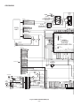
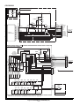
CD-RW5000
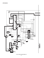
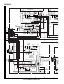
NOTES ON SCHEMATIC DIAGRAM
• Resistor:
To differentiate the units of resistors, such symbol as K and
M are used: the symbol K means 1000 ohm and the symbol
M means 1000 kohm and the resistor without any symbol is
ohm-type resistor. Besides, the one with “Fusible” is a fuse
type.
• Capacitor:
To indicate the unit of capacitor, a symbol P is used: this
symbol P means pico-farad and the unit of the capacitor
without such a symbol is microfarad. As to electrolytic
capacitor, the expression “capacitance/withstand voltage”
is used.
(CH), (TH), (RH), (UJ): Temperature compensation
(ML): Mylar type
(P.P.): Polypropylene type
• Schematic diagram and Wiring Side of P.W.Board for this
model are subject to change for improvement without prior
notice.
REF. NO
DESCRIPTION
• The indicated voltage in each section is the one measured
by Digital Multimeter between such a section and the chassis with no signal given.
1. In the tuner section,
( ) indicates AM
< > indicates FM stereo
2. In the main section, a tape is being played back.
3. In the deck section, a tape is being played back.
( ) indicates the record state.
4. In the power section, a tape is being played back.
5. In the CD section, the CD is stopped.
• Parts marked with “
”(
) are important for
maintaining the safety of the set. Be sure to replace these
parts with specified ones for maintaining the safety and
performance of the set.
POSITION
REF. NO
ON—OFF
SW761
TAPE
POWER
ON—OFF
SW762
TUNER
ON—OFF
OPEN/CLOSE
ON—OFF
SW763
CD
ON—OFF
PANEL OPEN/CLOSE
ON—OFF
SW764
CD-R
ON—OFF
CD/CD-R
ON—OFF
ON—OFF
NSW1
PICKUP IN
SW701
SW705
SW710
DESCRIPTION
POSITION
ON—OFF
SW711
VOLUME DOWN
ON—OFF
SW765
SW712
VOLUME UP
ON—OFF
SW766
TRACK EDIT
SW720
CD 1 EJECT
ON—OFF
SW767
CD-R RECORD
ON—OFF
SW721
CD 2 EJECT
ON—OFF
SW768
RECORD MODE
ON—OFF
SW722
CD 3 EJECT
ON—OFF
SW769
HIGH/NORMAL
ON—OFF
SW723
CD 4 EJECT
ON—OFF
SW772
EQUALIZER MODE
ON—OFF
SW724
CD 5 EJECT
ON—OFF
SW773
X-BASS
ON—OFF
SW725
CD 6 EJECT
ON—OFF
SW774
DISPLAY CHARACTER
ON—OFF
SW730
CD 1 PLAY
ON—OFF
SW775
MENU
ON—OFF
SW731
CD 2 PLAY
ON—OFF
SW776
NAME TOC EDIT
ON—OFF
SW732
CD 3 PLAY
ON—OFF
SW777
DELETE
ON—OFF
SW733
CD 4 PLAY
ON—OFF
SW778
ENTER
ON—OFF
SW734
CD 5 PLAY
ON—OFF
SW780
CD-R OPEN/CLOSE
ON—OFF
SW735
CD 6 PLAY
ON—OFF
SW783
PLAY MODE
ON—OFF
SW750
AUTO MARKER
ON—OFF
SWB101
DISC DETECT 1
ON—OFF
SW751
ERASE
ON—OFF
SWB102
DISC DETECT 2
ON—OFF
ON—OFF
SWB103
DISC DETECT 3
ON—OFF
SW752
FINALIZE
SW753
FAST REVERSE
ON—OFF
SWB104
MODE 1
ON—OFF
SW754
FAST FORWARD
ON—OFF
SWB105
MODE 2
ON—OFF
SW755
TAPE RECORD
ON—OFF
SWB106
MODE 3
ON—OFF
SW756
PLAY/PAUSE
ON—OFF
SWB107
MODE 4
ON—OFF
SW757
STOP
ON—OFF
SWB108
MODE 5
ON—OFF
SW758
PLAY
ON—OFF
SWB109
TRAY 1
ON—OFF
SW760
AUX
ON—OFF
SWB110
TRAY 2
ON—OFF
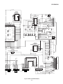
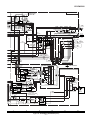
TYPES OF TRANSISTOR AND LED
2SA1015 GR
FRONT 2SA562 Y
2SB561 C
VIEW
2SB562 C
2SC1740 R
DTC363 TS
KRA102 M
E C B KRA107 M
(S) (G) (D) KRC102 M
(1) (2) (3)
KRC104 M
KRC107 M
KTA1046 Y
KTC2026
KTC3194 Y
KTC3203 Y
KTA1266 GR
KTC3199 GR
FRONT
VIEW
FRONT
VIEW
B C E
2SD2012
– 25 –
HLMP1700
K5052C
K5052UL
L1154GDA
L934MBC5
LNG995PF
1
2
3
SVC211C
SVC348S
CD-RW5000
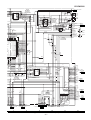
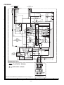
V
SWITCHING
Q351
TUN_L
13 MO/ST
14 L-CH OUT
(FM/AM)
12
PHASE
TUN_R 15 R-CH OUT
X351
456kHz
IC303
LA1832S
FM IF DET./FM MPX./AM IF
PHASE 11
FM DET 8
18 FM/AM OUT
GND 5
16 MPX IN
IF OUT 10
17 MPX
VCO
VCC 9
A_+B
CF351
FM IF
STEREO 7
SD 6
CF352
3
2
1
AM IF
19 AM LOW CUT AM IF IN 4
VSM
SWITCHING Q360
20 VSM
21 AM RF IN
T351
22 FM AFC
AM IF
REG 3
A_+B
23 AM OSC IN AM MIX OUT 2
24 AM OSC OUT FM IF IN 1
+B
FM
MUTE
LEVEL
12 IF IN ST IND 11
13 IO2 MO/ST 10
14 NC MUTE 9
VR351
10K(B)
15 AM IN MW 8
16 FM IN FM 7
17 VDD
A_+B
18 PD
AM
ANTENNA
T306
AM OSC.
+B
CL 5
DI 4
20 AOUT CE 3
21 VSS NC 2
Q371
C2B_DO
C2B_CL
C2B_DI
C2B_CE
22 X OUT X IN 1
X352
4.5MHz
T312
BAND
PASS
FILTER
6
5
4
3
2
1
TP301
Q302
T311
FM OSC.
ERAS
HEAD
OSC BUFF
VD302
SVC211C
+B
RECOR
PLAYBA
HEAD
L312
FM RF
3
BF301 2
1
AM GND FM
FM IF
L-CH R-CH
9
8
7
IC302
LC72131
PLL(TUNER)
VT_CK
VD303
SVC211C
IC301
TA7358AP
FM FRONT END
T306
DO 6
IC302
LC72131
VD301
19
AIN
CF302
FM IF
10.7MHz
3
2
1
SWITCHING
SO301
ANTENNA
TERMINALS
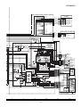
Figure 26 BLOCK DIAGRAM (1/6)
– 26 –
CD-RW5000
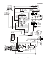
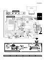
l
Q507
REC_R-CH
k
j
Q508
8
4 7
VSM
1
–
2 3
+
+
–
5 6
C2B_DO
C2B_CL
C2B_DI
C2B_CE
REC_L-CH
+B
-B
REC_L-CH
IC501
BU4066BCF
INPUT
SELECTOR
IC503
NJM4558M
OPE AMP.
4
TUNER
TAPE_R 15 R3
DECK
L3 10
AUX_R 16 R4
AUX
L4 9
L2
11
RSEL0
IC502
RIN
–
+
RTRE
LIN
LTRE
LBASS
RBASS
ROUT
LOUT
7
CD-RW MUTE
TAPE_L
Q504
Q503
AUX_L
CD-R_SEL
AUX_SEL
REC_L-CH
Q402
AUX_R
6
5
5 3 6 9 12 10 13 2
–
+
+
–
IC402
BU4066BCF
INPUT
SELECTOR
4
7
+
–
–
+
+B
VSS 3
CCB
INTERFACE
23 VDD
CE
CLK
DI
8
2
11
1
1
7
IC401
NJM4558M
OPE AMP.
8
1
–
24
4
+
+
–
VREF
Q
Y
Q401
14
22
1
2
3
TUNER_L
LSEL0 8
+
–
21
MD_RCH
MD_LCH
L1 12
–
+
+
–
20
1
5 3 6 9 12 10 13 2
TUNER_R 14 R2
R_CH
11
CD_L
CD
19
8
i
h
g
14
CD_R 13 R1
18
CD_L
7
IC502
LC75341
AUDIO PROCESSOR
17
CD_R
A_GND
TO MICOM SECTION
X W V U T S R O
TO MICOM SECTION
PB_MUTE
VSM
C2B_DO
C2B_CE
C2B_DI
C2B_CL
D_GND
S-MUTE
TAPE_L
TO MICOM
SECTION
A_GND n
TAPE_R m
TO MICOM SECTION
4
2 3 5 6
R-CH
IC102
BA3126N
HAED
SELECTOR
8
3
7
Q501
L_CH
JK501
R-CH
PHONO
INPUT
L-CH
TAPE_L-CH
L-CH
1
TAPE_R-CH 2
A_GND
3
REC_R-CH
4
REC_L-CH
5
REC_MUTE
6
REC_CONT
7
REC_BIAS
8
+B
4
5
6
REC MUTE
Q120
Q119
SWITCHING
CNP102
REC MUTE
Q101
Q102
M_+10V
+B
A_+10V A
A_GND B
C
BIAS_GND D
R-CH
L-CH R-CH
ERASE
HEAD
RECORD/
PLAYBACK
HEAD
1
2
3
4
5
6
1
2
3
4
5
6
1
2
3
4
5
6
7
CNP101
ERASE
1
M_GND
2
T2_R1 R-CH
3
T2_R2
4
A_GND
5
T2_L2
6
T2_L1
7
23
22
21
20
19
–
112K
+
Hich=T1
+
112K
–
1
L-CH
2
3
4
18
6
16
–
56K
+
Hich=CHROME
+
56K
–
IC101
5
17
7
8
9
15
Nor/CrO2
24
ALC
10
13
14
RIPPLE Vcc
ALC
11
GND
12
Q114
SWITCHING
IC101
AN7345K
PLAYBACK AND
RECORD/PLAY BACK
AMP.
BIAS OSC.
Q116
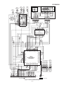
Figure 27 BLOCK DIAGRAM (2/6)
– 27 –
Q115
CNS940
2
Q509
SWITCHING
A_GND
A_+B
R_CH
A_GND2
AUX
INPUT
L-CH
FROM MAIN PWB
9
R_CH
f
e
d
c
b
a
TO POWER SECTION
1
Q502
A_-B
TO MICOM SECTION
SYSTEM MUTE
CD-RW5000
UNA901
DIGITAL
INPUT
CNP975
FROM
CD PWB
EBU GROUND
EBU SIGNAL(INPUT)
SCREEN
EBU GROUND
EBU SIGNAL(OUTPUT)
SCREEN
IC926
TC7WU04F
INVERTOR
CNP912
GROUND(CASE)
GROUND(CASE)
RESET
REQKBE
+B
I2C-CLOCK
GROUND(D)
+B
I2C-DATA
7
8
UNA902
DIGITAL
OUTPUT
+B
CST_SW
CASSETTE
SWITCH
F_REC
R_REC
12
12
1
11
12
CAM SW
B-FP SW
TUNER CL
CE
CST SW
DEST_IN
SPAN
CD MUTE
CLK
DATA
LCK1
LCK2
LCD DB4
TEST/Vpp
+B
Q905
FFC970
11
KEY 4
SOLENOID DRIVER
1
10
1
2
10
9
8
7
6
5
4
3
2
12 1
SOL
Q906
RUN_PUL
Q907
+B
+B
RUN PULSE
Q908
CAM-SW
+B
MOTOR DRIVER
Q909
MOTOR
+5V
CST-SW
SIDE-A
SIDE-B
g h i
TO AUDIO SECTION
Figure 28 BLOCK DIAGRAM (3/6)
– 28 –
A_GND
O Q P X Y U V W T R S d
TO AUDIO SECTION
f
c b a
TO AUDIO SECTION
R CH
A_GND
A_GND
A_+10V
A_+10V
CD_GND
CD_GND
CD B
–
+5V SENSOR
–COM
IC905
L CH
+
3
R_CH
A_GND2
L_CH
M
M
NC
NC
+B
Q901
PB_MUTE
CD-R_SEL
CD_MUTE
VSM
AUX_SEL
TAPE
MOTOR
+B
IC905
KIA7042AP
RESET
CD_L
PLAY
SWITCH
KEY 0
+B +B
CD_RES
CD_CCE
CD_BUCK
CD_BUS3
CD_BUS2
CD-RW
CD_BUS1
T-MO_REV
CD_BUS0
T-MO_FOR
CD_L
PU-IN
A_GND
C-MO_REV
CD_R
C-MO_FOR
CD_GND
CD_GND
CD_+B
CD_+B
1
2
3
4
5
6
7
8
9
KEY 1
KEY 2
51 52 53 54 55 56 57 58 59 60 61 62 63 64 65 66 67 68 69 70
SOLENOID
+SOL
SENSOR OUT
PLAY SW
+MTR
AVDD A
50
Vref 0
49
A_GND
CD_R
9
8
7
6
5
4
3
2
1
49 SP RLY
50 POWER KEY
48 PROTECT
CNP970
TO CD PWB
33
32
31
30
29
28
27
26
25
24
23
22
NC 21
20
19
18
17
16
15
14
13
12
11
10
47 SYS STOP
GND
FH_C-SW_B
FH_C-SW_A
FH_A-SW_E
FH_A-SW_D
FH_A-SW_C
FH_A-SW_B
FH_A-SW_A
FH_T-SW_A
FH_T-SW_B
FH_T-SW_C
CD-SW
TUNER DO
46 JOG-B
CNP901
TUNER DI
44 REMOCON
45 JOG-A
K-DATA/TX
42 XT1
43 RESET
CD-RW MUTE
MD-DSCK
41 XT2
X902
32.768kHz
MD-DATA/RX
MD_RCH
MD_LCH
1
2
3
IC901
IX0355AW
SYSTEM
MICROCOMPUTER
MD RESET
AVref1
40 VSS
LEVEL_R
39 X1
AVSS
38 X2
C2B_DI
C2B_CE
C2B_DO
C2B_CL
S-MUTE
D_GND
A_+B
A_-B
TO AUDIO SECTION
37 VDD
+B
X901
8MHz
Q911
LCD R/W
LCD RS
POWER RLY
N.C.
LCD DB7
MD SERCH
36 C FUTA OP
Q910
30
29
28
27
26
VSM
34 SYS MUTE
35 C FUTA CL
LCD DB5
32 TIMER LCD
33 BACK LED CONT
A-IN(REC)L-CH
GROUND(A)
A-IN(REC)R-CH
A-OUT(PB)R-CH
A-OUT(PB)L-CH
LEVEL_L
CNP914
LCD DB6
30 29 28 27 26 25 24 23 22 21 20 19 18 17 16 15 14 13 12 11
31 LCD E
5
4
3
2
1
1
2
3
4
3
2
1
5
6
KEY 3
1
2
3
4
5
6
7
CD-R
UNIT
1
2
3
Vcc 14
13
12
11
10
9
8
1
2
3
4
5
6
7 GND
IC921
74HCT00F
DIGITAL SIGNAL
SWITCH
CNP911
1
2
3
4
5
6
2
CD DOUT 1
1 2 3 4 5 6 7 8 9
CD-RW5000
DIG_SEL
IC912
BU2092F
OUTPUT
EXPANDER
+B
+B
+B
IC702
OUTPUT EXPANDER
BU2092F
13 Q8
12 Q7
11 Q6
10 Q5
+B
CD PICK IN 94
CD RW 93
CD RESET 92
FH A-SW A
FH A-SW B
SW750~SW758
SW760~SW769
LED_6
SW783,
SW772~SW778
JOG701
JOG DIAL
83
CNP931
+B
1 A_+B
+B
2 D_+B
3 D_GND
4 REMOCON
5 POW_KEY
6 POW_IND
7 DATA
8 CK
9 LCK
10 KEY1
11 KEY0
82
81
D_+B
69 70 71 72 73 74 75 76 77 78 79 80
IC922
BA3835F
BAND PASS FILTER
1
2
3
4
5
6
7
8
9
IC913
KIA7805P
VOLTAGE REGULATOR
+B
1
IC913
LED770
+B
CNS770
A_+B
7
KEY2
6
KEY3
5
KEY4
4
D_GND
3
2 JOG-A
JOG-B
1
LED754
LED755
LED_5
LED756
LED757
LED_4
LED_1
CD CCE 86
FH C-SW A 85
FH C-SW B
84
LED_3
CD BUS2 89
CD BUS3 88
FH A-SW C
LED758
LED759
CD BUS1 90
FH A-SW D
FH A-SW E
CD-R CLK
MD SID
MD LOAD SW
Q708
LED772
LED783
LED786
+B
CD BUCK 87
MD DSTB
CD-R DATA
Q720
Q722
Q724
FH M A- 96
FH M A+ 95
SW711,SW712,
SW720~SW725
+B
LED_EG
LED_1
LED_2
LED_3
LED_4
LED_5
FH M B- 98
LED_2
T-SOL
T-MOTOR
DEST_OUT1
DEST_OUT2
A-FP SW
VDD
RUN PULSE
CAM SW
B-FP SW
Q721
FH M B+ 97
81 FH T-SW A
TUNER CL
SW710,SW780,
SW730~SW735
11
Q723
CD BUS0 91
TUNER DO
Q1 6
Q2 7
Q3 8
Q4 9
VSS 100
REC MUTE 99
83 FH T-SW C
82 FH T-SW B
CNS720
A_+B
1
D_+B
2
D_GND
3
REMOCON
4
POW_KEY
5
POW_IND
6
DATA
7
CK
8
LCK
9
KEY1
10
KEY0
SW701
POWER
+B
Q725
1 2 3
+B
LCK 4
Q0 5
IC702
14 Q9
3 REC BIAS
2 REC
1 PB MUTE
RX701
REMOTE
SENSOR
18 VDD VSS 1
__
17 OE DATA 2
16 Q11 CLOCK 3
15 Q10
12 11 10 9 8 7 6 5 4 3 2 1
LED731
VDD 18
VSS
OE 17
DATA
SW12 16
CLK
LCK
SW11 15
NC
SW10 14
NC
SW9 13
NC
SW8 12
NC
SW7 11
CD-R_SEL SW5 10
1
2
3
4
5
6
7
8
9
BIASC GND 18
VREFC AOUT 17
RREF TEST 16
N.C. 15
N.C.
DIFOUT SEL 14
N.C.
N.C. 13
C 12
CIN
B 11
AIN
A 10
Vcc
CNP934
1 JOG-B
2 JOG-A
3 D_GND
3
+B
KEY4
KEY3
KEY2
A_+B
4
5
6
7
2
+B
+B
8 9 10 11 12 13 14 15 BI960
1 2 3 4 5 6 7 8
BI950
l m
j
k
A_GND
REC_RCH
REC_LCH
TAPE_L
TAPE_R
REC_BIAS
REC_CONT
REC_MUTE
REC_LCH
REC_RCH
A_GND
TAPE_R
TAPE_L
CD_GND
CD_GND
CD_+B
CD_+B
M_GND
M_GND
M_+B
M_+B
FAN_CTL
SP_DET
SP_RLY
UN_SW 5V
FAN
PROTECT
SP_RLY
+B
AC_RLY CTL POWER_RLY
A_-B
D_GND
D_GND
DIMMER
m
TO AUDIO SECTION
8 7 6 5 4 3 2 1
BI940
8 7 6 5 4 3 2 1
CNS940
+B
CNP703 1
VLOUT
1
NC 2
NC 3
NC 4
NC 5
NC 6
VCC
7
GND
8
/RD
9
/WR 10
RS 11
/CS
12
/RESET
13
DB4
14
DB5 15
DB6 16
DB7 17
Q707
SCL
SDA
IC701
TA7291S
LOADING
MOTOR DRIVER
IC701
Q706
17
OPEN_SW
D_GND
1 2 3 4 5 6 7 8 9
CLOSE_SW
CNP806
TO POWER
PWB
CNP807
TO POWER PWB CNP102
PNL_OP
MOTOR_+
PNL_CL
Figure 29 BLOCK DIAGRAM (4/6)
– 29 –
MOTOR_–
LCD710
LCD DISPLAY
LED735,LED737,
LED738
M
MO700
CONTROL
PANEL MOTOR
SW705
OPEN/CLOSE
CD-RW5000
Q200
MO200
FAN
MOTOR
+
Q212
JK701
HEADPHONES
FAN MOTOR
DRIVER
M
SO201
+
Q210
+
RY202
+
+
SP L-CH
GND
MAIN
SP L-CH
SP L-CH
SO201
GND
SPEAKER
SP L-CH SUB TERMINALS
WOOFER
SP R-CH
GND
SP R-CH
AC POWER
SUPPLY
CORD
AC 120V,
60Hz
SP R-CH
GND
MAIN
SP R-CH
L802
LINE FILTER
RY801
F807
5A 125V
Q209
RY201
T801
MAIN POWER TRANSFOMER
T802
SUB POWER
TRANSFORMER
M+10V
Q211
TF
Q208
15
D806
D805
D814
D815
D813
2
1
D812
F801
2.5A 125V
D807
-B
D804
F808
2.5A 125V
+B
LOW
HIGH
5
-B
+B
D817
D816
7
6
3
IC808
D811
D810
D809
D808
F804
5A 125V
F803
5A 125V
+B
Q204
Out
Ch2
F806
4A 125V
8
-B
-B
9
F805
4A 125V
–Vcc
IC202
STK40204(2Ch)
POWER AMP.
10
+Vcc
11
Out
Ch2
+B
+
Q203
12
MICON +5V
13
+B
F802
3.15A 125V
–
Ch2
14
IC808
KIA7805AP
CONSTANT VOLTAGE
+B REGULATOR
Q207
NC
VOLTAGE
REGULATOR
Q806
+
1
+B
–
3
2
Q807
-B
Ch1
4
-B
RELAY
DRIVER
15
Q206
–
Ch2
+B
14
13
Q205
+
12
IC802
KIA7810AP
VOLTAGE
REGULATOR
1
Q201
IC203
KIA4558P
OPE AMP.
8
–
Q809
Q801
VOLTAGE
REGULATOR
Q803
1
IC203
3
4
–
5
IC803
-B
1
IC801
2
IC801
KIA7812AP
CONSTANT
VOLTAGE
REGULATOR
3
+5V
+5V
GND
GND
GND
+12V
-8V
-B
BIAS_GND
A_GND
M_+10V
-B
A_+10V
A B C D
-8V
NC
FAN_CTL
SP_DET
SP_RLY
UN_SW 5V
+B
D_GND
D_GND
AC_RLY CTL
1
+B
3
2
+B
6
5
4
+B
IC803
NJM431L
VOLTAGE
REGULATOR
L-CH
A_GND2
R-CH
A_GND
A_GND
A_+10V +B
A_+10V +B
CD_GND
CD_GND
CD_+B
CD_+B
M_GND
M_GND
M_10V
M_10V
–
Ch1
Out
Ch1
2
3
6
+B
2
Q810
7
+
Q202
7
+
+B
Q805
VOLTAGE
REGULATOR
2
+B
1
8
3
+B
-B
+B
+Vcc
IC201
STK40271(2Ch)
POWER AMP.
Out
Ch2 10
–Vcc 9
+B
IC802
+B
11
TO DECK SECTION
CNP806 1 2 3 4 5 6 7 8 9 10 11 12 13 14 15
TO MAIN PWB BI960
1 2 3 4 5 6 7 8
7 6 5 4 3 2 1 CNP808
CNP807
TO MAIN PWB BI950A
Figure 30 BLOCK DIAGRAM (5/6)
– 30 –
FROM CD-R UNIT CNS808S
+
CD/CD-RW_SEL
IC2
TC9490F
SERVO/SIGNAL
CONTROL
TO MAIN PWB
– 31 –
PDO
PVDD
/UHSO
/HSO
SBSY
SFSY
DATA
CLCK
SBOK
DVSS
DVDD
IPF
DOUT
AOUT
LRCK
BCK
Figure 31 BLOCK DIAGRAM (6/6)
NC
TRAY SWITCH
CNP1
1 2 CNS12
CNP975 TO MAIN PWB
SWB101
SWB102
SWB103
IC6
+B
C
F
B
A
E
VREF
+5V
SWITCHING
IC6
TA2147F
SERVO PRE
AMP.
TR–
TR+
FO+
FO–
GND
PD
VR
LD
1
2
3
4
5
6
7
1
2
3
4
5
6
7
8
1
2
3
4
5
6
7
1
2
3
4
5
6
7
8
C
F
B
A
E
1/2V
+5V
TR–
TR+
FO+
FO–
GND
PD
VR
LD
LTOH41M1
TR–
ACTUATOR
FO–
FO+
TR+
CAM
SWITCH
Q4
Q5
Q3
DZ2
Q1
LPF
VCC
LD
MON
GND
E
A
B
F
C
+
–
+
–
+
–
+
–
+
–
1/2VCC
PICKUP UNIT
M
SWB104
SWB105
SWB106
SWB107
SWB108
SWB109
SWB110
SBAD 12
TEO 11
TEN 10
TEB 9
SEL 8
LDO 7
MDI 6
TNI 5
TPI 4
FPI 3
FNI 2
VCC 1
BIAS
+
–
1 2 3 4 5 6 7 8 9 10 11 12 13 14 15 16
13 GVSW
14 VRO
15 FEO
16 FEN
17 RFRP
18 RFIS
19 RFGO
20 RFGC
21 AGCI
22 RFO
23 RFN
24 GND
VCC
LOADING1
VREFSW
BIAS
PREVCC
POWVCC
BIAS
1 2 3 4 5 6 7 8 9 10 11 12 13 14 15 16
SL+ +
SL–
–
MOB2
TRAY
MOTOR
GND(D)
TRAY_A
TRAY_B
TRAY_C
GND(D)
CANA_A
CANA_B
CANA_C
CANA_D
CANA_E
CANB_A
CANB_B
32
31
30
29
28
27
26
25
24
23
22
21
20
19
18
17
SP+ +
SP–
+
M
GND
FOO
TRO
VREF
RFGC
TEBC
SEL
AVDD3
FMO
DMO
DVSS
DVDD
TESIN
XVSS
XI
XO
XVDD
TEZI
TEI
SBAD
FEI
RFRP
RFZI
RFCT
AVDD
RFI
SLCO
AVSS
VCOF
PVREF
LPFO
LPFN
TMAX
VCC
LOADING2
DVSS
RO
DVDD
DVR
LO
DVSS
ZDET
VSS
BUS0
BUS1
BUS2
BUS3
BUCK
/CCE
/RST
VDD
LEVEL
SHIFT LEVEL
SHIFT
LEVEL SHIFT
BIAS
IC5
POWVCC
PREVCC
MUTE
49
50
51
52
53
54
55
NC
56
57
58
59
60
61
62
63
+B 64
LEVEL SHIFT
LEVEL
SHIFT LEVEL
SHIFT
BIAS
–
CD FUNC
TRAY_C
TRAY_B
TRAY_A
CANA_A
CANA_B
CANA_C
CANA_D
CANA_E
CANB_A
CANB_B
X1
16.934MHz
48 47 46 45 44 43 42 41 40 39 38 37 36 35 34 33
SWITCHING
32 31 30 29 28 27 26 25 24 23 22 21 20 19 18 17
+B
GND
PU-IN
M
9
8
7
6
5
4
3
2
1
BUS1
REGULATOR
+B
M
BUS2
BUS3
BUCK
/CCE
/RST
3.3V
IC5
BA5939S
FOCUS/
TRACKING/
SPIN/
SLED DRIVER
–
BUS0
GND
PU-IN
CD_L-CH
CD_R-CH
CD_GND
CD_+B
NSW1
PICKUP IN
NM1
NM2
SPINDLE SLED
MOTOR MOTOR
NC
MOB1
MAIN CAM
MOTOR
NC
NC
33
32
31
30
29
28
27
26
25
24
23
22
21
20
19
18
17
16
15
14
NC 13
12
11
10
CD-RW5000
CD-RW5000
+B
C321
100/16
C345
0.022
C346
0.022
0.8V
0.1V
1.8V
Q302
KTC3194 Y
OSC BUFF
C318
100P(CH)
T311
T312
FM IF
C2B_DO
R371
4.7V
R373
1K
R399
10K
0V
D
4.7V 4.7K
Q371
KTA1266 GR
SWITCHING
R374
1K
C311
100P(CH)
C312
100P
(CH)
C382
15P(CH)
C310
100P
(CH)
R372
1K
+B
C337
0.022
D352
DS1SS133
VDD 17
L351
100µH
9.2V
11 ST IND IF IN 12 0V
R378
82K
R360
4.7K
3
CF302
FM IF
10.7MHz
R323
68K
+B
R351
5.6K
C351
0.022
L353
1mH
C352
10/50
2V 1 FM IF IN AM OSC OUT 24 3V
4.6V
4.6V
2 AM MIX OUT AM OSC IN 23
2V
REG
C350
0.047
+B
2.4V
FM AFC 22
0.3V
AM RF IN 21
0V
VSM 20
CF352
1
C370
1/50
K
L
M
N
C319
0.1
+B
R391
390
DZ351
DZ5.1BSB
+B
C355
22P
(CH)
C396
100/16
VSM
A_+B
TUN_L
A_GND
TUN_R
R389
3.9K
C366
0.001
4.7V
C354
7 STEREO
0.022
R353
CF351 270 2.5V
8 FM DET
FM IF C399
X351
0.022 4.6V
2.1V 456kHz
9 VCC MPX VCO 17
C398
R356
100/16
2V
1K
3.9V
C356
0.001
C357
2.2/50
+B
L352
100µH
C2B_DI
C2B_DO
C2B_CL
C2B_CE
D_GND
C364
4.7/50
C365
0.022
C367 R350
1/50 2.7K
C395
0.022
TO AUDIO SECTION P33 10-A
E
F
G
H
I
J
C363
0.022
IC303
LA1832S
AM LOW
2.3V
4 AM IF IN CUT 19 2.1V
3 R352 0V
FM/AM 18
5 GND
OUT
C353 1K 4.7V 6
SD
0.022
2
+B
2V
C343
33P
(CH)
C361
0.022
T351
AM IF
R358
8.2K
C362
3.3/50
3
AM IF
+B
F
FM
MUTE
LEVEL
VR351
10K(B)
R393
1K
IC302
LC72131
PLL(TUNER)
R392
390
C331
0.047
C342
0.022
C386
330P
(CH)
+B
C332
0.022
R336
10K
R377
47K
R395
47K
C330
15P(UJ)
VD301
SVC348S
C387
0.022
R376
1K
10V
T302
AM
ANTENNA
C339
100P
(CH)
C334
15P(UJ)
1
2
C380
10/50
10 MO/ST IO2 13
Q360
2SB562 C
SWITCHING
E
4.7V
R379
2.2K
2.3V
7 FM FM IN 16
3.5V
8 MW AM IN 15 0V
4.1V
C385
9 MUTE NC 14
0.01
3.6V
4.7V
4.7V
10V
C397
2.3V
0.022
1 X IN X OUT 22
R381
0V 2 NC VSS 21 0V
10K
1.3V
0V
3 CE AOUT 20
C393
0V
C394
4 DI
1/50
47/16
0V
R380
5 CL
1.5K
C392
0.8V
AIN 19
0.001
4.7V
0.8V
6 DO PD 18
0.1V
C391 R384
47/16 5.6K
R385
5.6K
R383
5.6K
C335
330P(CH)
R382
150
C323
0.022
AM BAND
COVERAGE fL
T306
AM OSC.
2.3V
IC302
D304
DS1SS133
+B
C347
0.022
C381
12P(CH)
X352
4.5MHz
C338
0.001
D303
DS1SS133
R359
1.8K
R357
470K
10 IF OUT MPX IN 16
3.4V
C374
0.015
C368
1/50
11 PHASE
1.2V
R-CH OUT 15
1.2V
L-CH OUT 14
PHASE
3.4V
MO/ST 13 3.6V
12
(FM/AM)
C371
R355
C358
1/50
1/50
R361
18K
3.3K
R362 C372
18K 1/50
C384
0.001
+B
D302
DS1SS133
R309
10K
L342
2.2µH
+B
D301
DS1SS133
T311
FM BAND
COVERAGE fL
C324
4P(CH)
VD303
SVC211C
VT_CK
C2B_CE
C2B_DI
C2B_CL
R302
7 2.9V
10
8 3.6V
C326
3.6V
9
18P(CH)
FM OSC.
C327
0.1
+B
R345
4.7K
C
C305
5P(CH)
VD302
SVC211C C325
15P(CH)
C313
22P
(CH)
TP301
C341
0.1
L312
1
BAND
2 BF301 PASS
FILTER
3
C303
10P(CH)
0.8V
1
2 1.6V
3 3.6V
4 1.6V
5 0V
6 3.6V
C373
0.015
R363
1.2K
IC303
LA1832S
FM IF DET./FM MPX./AM IF
R364
1.2K
R354
3.9K
G
2
1
SWITCHING
3
Q351
KRC104M
R370
1K
MAIN PWB-A(1/3)
H
• NOTES ON SCHEMATIC DIAGRAM can be found on page 25.
1
2
3
AM TRACKING fL
R369
820
B
R327
33
C308
5P(CH)
R311
R313100K
R325
47K
C390
0.001
FMRF
33K
C317
0.001
R322
680
C389
0.001
D305
DS1SS133
D306
DS1SS133
C316
0.1
D310
DS1SS133
C304
0.01
C306
0.001
IC301
TA7358AP
FM FRONT END
C314
0.0047
C315
0.0047
R314
22
C301
0.001
C309
0.001
D311
DS1SS133
D312
DS1SS133
A
SO301
ANTENNA TERMINALS
FM GND AM
AM SIGNAL
FM SIGNAL
4
Figure 32 SCHEMATIC DIAGRAM (1/11)
– 32 –
5
6
CD-RW5000
R547
2.2K
R548
2.2K
C573
2.2/50
R591
47K
R592
47K
8
11
–
C446
22/50
R414
(6V)
(-6V) (-6V)
RECORD SIGNAL
R420 C449
330 0.1
R413
47K
47K
Y AUX_SEL
X VSM
W C2B_DO
V C2B_CE
U C2B_DI
T C2B_CL
S D_GND
R S-MUTE
Q CD-R_SEL
O PB_MUTE
(0V)
S-MUTE
+B
R544
47K
C529
10/50
C510
10/50
C512
0.1 (ML)
5V
C514
0.1(ML)
10V
C516
0.0027(ML)
5V
R532
R534
5V
3.9K
3.9K
C518
1/50
5V
C520
1/50 AUX_R
5V
C522
1/50 TAPE_R
5V
C524
1/50 TUNER_R
5V
C526
CD/CD-R_R
1/50
5V
C528
1/50
R526
1K
R528
2.2K
R530
3.9K
R552
47K
R538
1K
13
10
11
CD
C537
0.1
-B
C532
100P(CH)
Q508
DTC363 TS
0V 2
R540
10K
0V
4 8.2V
5 +
7
R542
6 –
0V
1.5K
0V IC503
C550
R541
+B
22/50
8 10V
1.5K 0V
2 –
1
C551
3 +
0V
22/50
0V
R539
C533
10K
47P
(CH)
C531
100P(CH)
C535
0.1
+B
L1
TUNER
L2
DECK
AUX
9
L3
L4
8
12
R533 0.0027(ML)
3.9K
5V
R531 C517
3.9K 1/50
5V
C519
AUX_L
1/50
5V
C521
5V
TAPE_L 1/50
C523
5V
TUNER_L 1/50
C525
5V
CD/CD-R_L 1/50
5V
R529
3.9K
7
C534
47P
(CH)
R1
R3
14
R2
15
LSEL0
LIN
LBASS
LTRE
LOUT
5V
5V
R507
22K
C511
0.1
C513
0.1(ML)
C515
C509
10/50(ML)
C564
0.1
IC502
LC75341
6
5
4
C563
10/50
16
R4
RIN
RSEL0
RTRE
ROUT
RBASS
17
IC503
NJM4558M
OPE AMP.
C536
10/50
5V
VDD
VREF
–
+
CCB
INTERFACE
VSS
3
0V
CE
18
+
–
10V
0V
0V
DI
0V
–
+
–
+
2
19
+
–
1
20
+
–
CLK
21
22
–
+
23
24
+
–
+B
R536
47K
IC502
LC75341
AUDIO PROCESSOR
R525
1K
+B
PB_MUTE
R543
47K
+B
CD SIGNAL
(0.7V)
2
3
3 (6V) R423 (7.6V)
1 Q402
1 1K
(7.6V) KRA107 M
(6V)
2 (-6V)
R424
47K
+B
R524
1K
VSM
TUN_L
A_GND
TUN_R
A_+B
C2B_CE
C2B_DI
C2B_CL
C2B_DO
D_GND
PLAYBACK SIGNAL
R416
47K
R415
47K
(0V)
IC402 (0V)
BU4066BCF
INPUT
SELECTOR
FM SIGNAL
R421
330
(8.8V)
14 (7.6V)
5 3 6 9 12 10 13 2 (0V)
(6V)
R410
33K
(-6.9V)
4
R422
IC402 47K
C574
2.2/50
C440
0.0022
C444
22/50
MAIN PWB-A (2/3)
C448
0.1
8
7 (0V) IC401
C445
22/50
1 (0V)
7 (-6V)
(0V)
(0V)
(0V) 4
1
R408
390K
J
R551
47K
C527
1/50
R537
1K
0V
1
3 3.6V
3.6V 3
C566
22/50
R582
22K
1
0V
0V 2
Q507
DTC363 TS
C530
10/50
R535
47K
R527
2.2K
-B
(0V)
(0V)
2.6V
C598
3 2.6V 0.0027
CD
(-6V) (-6V)
(6V)
(6V) 5 3 6 9 12 10 13 2 (0V)
SWITCHING
Q502
Q501
KTC3199 GR KTC3199 GR
SYSTEM MUTE
+B
R501
330
R513
5.6K R511
5.6K
(0V)
(0V)
IC501
BU4066BCF
INPUT
SELECTOR
DZ502
MTZJ8.2B
R523
330
(-6V)
(6V) 3
R522
330
R517 R516
1K
47K
(7.6V) 2
Q503
KRA107 M
1
(7.6V)
3 (0V)
R512
5.6K
-B
-B
a b c d e f
TO MICOM SECTION
P34 6-H
7
(0V)
R514
5.6K
1
1
8
g h i
2 1
TO MICOM SECTION
P34 4-H
TO MICOM SECTION
P35 11-H
9
10
Figure 33 SCHEMATIC DIAGRAM (2/11)
– 33 –
j
k
3
TAPE_L
TAPE_R
A_GND
0V
11
(-6V)
Q504
KRC107 M
MD_LCH
MD_RCH
0V
8
CD-R_R
0V
(0V) 4
R515
47K
(-6V) 2
(7.6V)
CD_L
A_GND
CD_R
0V
7
0.7V
CD-R_L
C501 C502
0.001 0.001
0.7V
14
R504
2.2K
L_CH
A_GND2
R_CH
R502
330
A_+B
A_GND
A_-B
SYSTEM MUTE
R503
2.2K
CD-RW MUTE
1
REC_LCH
REC_RCH
C597
0.0027
(0V)
2 0V
C565
0.1
C506
47/25
C508
0.1
C507
47/25
Q509
KRA107 M
C503
22/50
l m n
TO MICOM SECTION
P35 10-H
11
12
TO MICOM SECTION
P34 5-H
L502
2.2µH
+
C438
0.0082
C443
22/50
+B
L501
2.2µH
R412
6.8K
(0V)
(0V)
C439
0.0022
L411
2.2µH
C442
150P(CH)
Q401
KRC107 M
C541
390P
R411
6.8K
2 3 5 6
+
L M N K H E G F I
R406
1K
(0V)
(0V)
R404
47K
C412
680P
R403
47K
(0V)
C437
0.0082
L412
2.2µH
–
C411
680P
R405
1K
C441
150P
(CH)
R407
390K
R402
2.7K
R401
2.7K
C400
0.001
C540
390P
R549
39K
TO TUNER SECTION
P32 1-G
IC401
NJM4558M
OPE AMP.
R409
33K
D508
DS1SS133
D507
DS1SS133
CHASSIS
GND
C562
0.1
C599
0.001
R550
39K
JK501
AUX
PHONO
INPUT
INPUT
L-CH R-CH L-CH R-CH
CD-RW5000
MAIN PWB-A (3/3)
C
1
(C
C950
150P
(CH)
EX-DATA R1031 1K
EX-CLK R1007 1K
R1008 1K
LCK1
FM SIGNAL
A
PLAYBACK SIGNAL
R1141
1K
RECORD SIGNAL
CD SIGNAL
+B
+B
SPAN SEL.
R1101
R1102
R1103
R1104
R1022
R1124
10K
R
10
R1106
R1107
R1108
R1109
22K
22K
22K
10K
47K
R1068
10K
10K
10K
10K
10K
+B
B
L901
100µH
33
R1046
12K
IC905
KIA7042AP
RESET
3 IC905 1
5V
5V
Q901
KRC102 M C905
5V 3.3/50
2
4.4V
3
2 0V
C904
0.01
F
R1143
1M
D907
DS1SS133
0V 1
C903
0.1/50
C906
0.1
RUN_PUL
R908 1K
R907 1K
1K VPP
1K LCK2
1K LCK1
1K EX-CLK
1K EX-DATA
1K
1K
1K C2B_CE
1K CST-SW
1K CAM-SW
1K SIDE-B
1K SIDE-A
5V VDD
0V DEST OUT2
5V RUN PULSE
5V CAM SW
5V B-FP SW
5V A-FP SW
0V CE
5V CST SW
SPAN
CD MUTE
0V DEST_IN
0V CLK
0V DATA
0V LCK2
0V TEST/Vpp
(0.3V) LCD DB4
0V LCK1
MD SID
LCD-RW/CDR-DATA (4.8V)
MD DSTB
TUNER CL 0V
TUNER DO 4.8V
MD LOAD SW
TUNER DI 0V
MD-DSCK
K-DATA/TX
MD RESET
AVref1 5V
MD-DATA/RX
MD SERCH
AVSS 0V
0V
0V
KEY 4 5V
R945 100
TX
R927 100
MDDSCK R967 1.8K
C2B_DI R968 1K
C2B_DO R969 1K
C2B_CL R970 1K
LOAD_SWR971 1K
DSTB R972 1K
CDR-DATA R973 220
SID R974 220
RESET R963 1K
RX
SERCH R962 1.8K
1K
1K
1K
KEY3 R956 1K
KEY4 R957 1K
LEVEL_LR958 1K
VSM R959 1K
LEVEL_RR960 1K
+B
D906
R1003
DS1SS133 4.7K
R1001
47K
KEY2 R955
C998
22/10
KEY1 R954
C945 C916
0.1 0.1/50
+B
C901
1000/6.3
50 POWER KEY 5V
76 FH A-SW E 0.2V
54 KEY 1 5V
55 KEY 2 5V
C917 51 52 53 54 55 56 57 58 59 60 61 62 63 64 65 66 67 68 69 70 71 72 73 74
0.1/50
KEY0 R953
R946
1K
77 FH A-SW D 0.2V
53 KEY 0 5V
KEY 3 5V
PROTECT 5V
49 SP RLY 5V
NC
CD_RES
CD_CCE
CD_BUCK
CD_BUS3
CD_BUS2
CD-RW
CD_BUS1
T-MO_REV
CD_BUS0
T-MO_FOR
CD_L
PU-IN
A_GND
C-MO_REV
CD_R
C-MO_FOR
CD_GND
CD_GND
CD_+B
CD_+B
JOG-B 5V
SYS STOP 5V
KDATA
9
8
7
6
5
4
3
2
1
E
R1066
10K
REMOCON 5V
JOG-A 5V
80 FH A-SW A 0.2V
79 FH A-SW B 0.2V
78 FH A-SW C 0.2V
51 AVDD A 5V
52 Vref0 5V
C964
0.1/50
R1099
47K
MDDATA
P38 1-E
R1065
10K
RESET 4.4V
R1053 10K
R1054 10K
R1055 10K
R1056 10K
R1057 10K
R1058 100K
CNP1
RX_IN
JOG-A
JOG-B
PROTECT
SP_RLY
TO CD PWB
C943
0.1
R1044
22K
39
R941 40
X902 330K 41
32.768KHz
42
RES43
R943 R944 1K
44
1K
R965 1K
45
R966 1K
46
R947 1K
47
R948 1K
48
R995 1K
C941
22P
(CH)
7
4 DEST_OUT1 0V
30 LCD R/W (4.7V)
29 LCD RS (4.5V)
X1 2.3V 28 POWER RLY 0.8V
VSS 0V 27 N.C.
XT2 2.8V 26 LCD DB7 (1.3V)
XT1 2V 25 LCD DB6 (2.5V)
38 X2 2.6V
POWER
D
GND
FH_C-SW_B
FH_C-SW_A
FH_A-SW_E
FH_A-SW_D
FH_A-SW_C
FH_A-SW_B
FH_A-SW_A
FH_T-SW_A
FH_T-SW_B
FH_T-SW_C
CD-SW
5V BACK UP
33
32
31
30
29
28
27
26
25
24
23
22
21
20
19
18
17
16
15
14
13
12
11
10
D905
DS1SS133
1
CNP901
FFC901
C902
0.1
8
IC901
3 REC BIAS 0V
IX0355AW 2 REC 0V
SYSTEM 1 PB_MUTE 5V
MICROCOMPUTER
37 VDD 5V
C942 X901
18P 8MHz
(CH)
VSM 0.3V
R1036
5.6K
1K
31 LCD E (4.6V)
1K 32 TIMER LCD 5V
1K 33 BACK LED CONT 5V
1K 34
SYS MUTE 5V
1K
35 C FUTA CL 5V
1K 36 C FUTA OP 0.2V
R1060 100K
R1035
5.6K
R929
R932
R933
R934
R935
R936
(2.5V) LCD DB5
30 29 28 27 26 25 24 23 22 21 20 19 18 17 16 15 14 13 12 11 10 9
LCD-E
LED-TIMER
DIMMER
S-MUTE
P-CLOSE
P-OPEN
R1004
10K
R1005
C995 C936
100P 100P
(CH) (CH)
C
1K
1K
R921
R920
R919
R918
R917
R983
R915
R914
R913
R912
R911
R910
R931
R930
LCD-RES
LCD-RW
R991 1K
POWER_RLY
R926 1K LCD-DB7
R925 1K LCD-DB6
R924 1K LCD-DB5
R923 1K LCD-DB4
+B
+B
D901
DS1SS133
R1125
10K
C1003
47/50
D902
DS1SS133
C907
10/50
R1002
100K
+B
CASSETTE
SWITCH
F_REC
R_REC
10
9
10
11
12
12
12
8
7
6
5
4
3
2
1
11.3V
R1013 0V 1 0V
47K
L910
47H 0V
C912
47/16
RUN_PUL
5V
R2133
470
CAM-SW
MOTOR DRIVER
11.4V
+B
R1014 MOTOR DRIVER
100K
11.3V
MOTOR
2
3
0V
Q908
2SB561 C R101511.3V 1 0V Q909
KRC107 M
820
+B
A_GND
+B
CST-SW
SIDE-A
SIDE-B
TAPE MECHANISM
ASSEMBLY (1/2)
g h i
H
X Y U V W T R S d f
O Q
c
b a
L CH
A_GND
R CH
A_GND
A_GND
A_+10V
A_+10V
CD_GND
CD_GND
CD +B
CST_SW
11
SOL
3
2
R1012
0V
1
1K
2 Q907
KRC107 M RUN PULSE
R_CH
A_GND2
L_CH
+5V SENSOR
–COM
–
12
+B
+B
VSM
AUX_SEL
C2B_DI
C2B_CE
C2B_DO
C2B_CL
S-MUTE
D_GND
A_+B
A_–B
+
1
11.3V
+B
+B
PB_MUTE
CD-R_SEL
M
M
NC
NC
1
C913 3
2.2/50
SOLENOID DRIVER
Q906
KRC107 M
R1011
100K
CD_L
A_GND
CD_R
PLAY
SWITCH
TAPE
MOTOR
FFC970
1
2
3
4
5
6
7
8
9
D910
DS1SS133
CNP970
SOLENOID
+SOL
SENSOR OUT
PLAY SW
+MTR
11.4V
0V
0V
Q905
2SB561 C
TAPE
MECHANISM
PWB-H
G
+
1 2 3 4 5 6 7 8 9
P33 12-C
P33 7-H
TO AUDIO SECTION
TO AUDIO SECTION
P33 9-H
• NOTES ON SCHEMATIC DIAGRAM can be found on page 25.
1
2
3
4
Figure 34 SCHEMATIC DIAGRAM (3/11)
– 34 –
5
6
CD-RW5000
CNP975
C957
150P
(CH)
IC912
BU2092F
OUTPUT
EXPANDER
C970
5V +B
VSS
VDD 18
0V
0.1
DATA
OE 17
0V
R1032 1K DIG_SEL
CLK
SW12 16 0V
R1052 1K AUX_SEL
LCK
SW11 15 2.8V
R1051 1K FAN
CD-SW
SW10 14
0V
R1050 1K PNL_OP
NC
SW9 13
0V
R1023 1K PNL_CL
NC
SW8 12
R1020
NC
SW7 11 P_CONT
1K
CD-R_SEL SW5 10
0V
0V
0V
0V
1.1V
1
2
3
4
5
6
7
8
0V
9
R1141
1K
IC912
BU2092F
LCD_RESET
C971
0.1
R1024
10K
(2.6V)
R1026
10K
(5V)
(2.4V)
(2.4V)
(5V)
(2.6V)
(0V)
(5V)
IC921Vcc 14
1
2
3
4
5
6
7 GND
(0.5V)
13
(0.5V)
12
(5V)
11
(0.5V)
10
(4.3V)
9
8
L912
2.2µH
IC921
74HCT00F
DIGITAL
SIGNAL
SWITCH
C974
0.1
C975
1/50
(5V)
CD-R_SEL
D951
DS1SS133
(2.6V)
R1135
2.7K
R1134
56K
(0V)
(0V)
R1137
4
220K
(2.6V)
3
(2.5V)
R1136 C1009
2
(2.5V)
330 0.022
1
5
(2.5V)
6
(2.5V)
7
8
IC926
CDR-DAT
CDR-CLK
1K RUN_PUL
1K
1K SOL
1K MOTOR
1K
1K REC_BIAS
1K REC_CONT
1K PB_MUTE
+B
(-6.1V) 3
5V REC MUTE 99R996
0V FH M B– 98
FH_T-SW_C
N1731AW
FH_T-SW_B
P38 3-B
1
FFC914
C952
10/50
C999
680P
R1078
3.9K
DSTB
R1040
10K
FH_T-SW_A
5
R1080 R1079
1.5K
1.5K
R1089 R1090
5.6K
5.6K
1K
1K
1K
1K
1K
R988
R987
R986
FH_A-SW_B R985
FH_A-SW_A R984
FH_A-SW_C
CNP911
EBU GROUND
FROM
EBU SIGNAL(INPUT) CD-R UNIT
SCREEN
CNS911A
EBU GROUND
EBU SIGNAL(OUTPUT) P38 3-A
SCREEN
FFC912
CNP912
1
1 GROUND(CASE)
2 GROUND(CASE)
3 RESET
4 REQKBE
P38 3-B
5 I2C-CLOCK
6 GROUND(D)
TO
7 I2C-DATA
7
CD-R UNIT
R1028
27K
0.2V FH T-SW A 81
FH
T-SW
A
FH_A-SW_E
FH_A-SW_D
R972 1K
R973 220
R974 220
CDR-CLK R975 220
SID
DSTB
(-6.1V) 3
0V VSS 100
R916 1K REC_MUTE
1K C-MO_FOR
R997 1K C-MO_REV
0V FH M B+ 97
R998 1K T-MO_FOR
0V FH M A– 96
R999 1K T-MO_REV
0V FH M A+ 95
R928 1K
PU-IN
5V CD PICK IN 94
R949 1K
CD-RW
5V CD RW 93
R982 1K CD_RES
0V CD RESET 92
R976 1K CD_BUS0
0V CD BUS0 91
R977 1K CD_BUS1
0V CD BUS1 90
R978 1K CD_BUS2
0V CD BUS2 89
R979 1K CD_BUS3
0V CD BUS3 88
R980 1K CD_BUCK
5V CD BUCK 87
R981 1K CD_CCE
5V CD CCE 86
R989 1K FH_C-SW_A
5V FH C-SW A 85
R990 1K FH_C-SW_B
0.2V FH C-SW B 84
R994 1K
0.2V FH T-SW C 83
R993 1K
5V FH T-SW B 82
R992 1K
IC926
TC7WU04F
INVERTOR
2 (0V)
2 (0V)
1 (0V) 1
Q910
DTC363 TS
Q911
DTC363 TS
1
72 73 74 75 76 77 78 79 80
CDR-DATA
UNA902
DIGITAL
OUTPUT
L915
2.2µH
LCD-E/CDR-CLK (4.6V)
MD DSTB
0.2V
MD SID
0.2V
LCD-RW/CDR-DATA (4.8V)
0.2V
0.2V
0.2V
2
C951
10/50
E 5V
3
1
2
3
A-IN(REC)L-CH
GROUND(A)
A-IN(REC)R-CH
A-OUT(PB)R-CH
A-OUT(PB)L-CH
CNP914
C914
0.1
R1077
3.9K
UT1 0V
AS 0V
4
0V T-MOTOR
5
UNA901
DIGITAL
INPUT
5
4
3
2
1
R908
R907
R906
R905
R904
R902
R903
R901
6
0V T-SOL
5V VDD
7
0V DEST_OUT2
5V A FP SW
8
5V RUN PULSE
0 9
1
2
3
1
2
3
4
5
6
C978
100P
(CH)
C1010
0.1
CNS12 FROM CD PWB
P38 1-G
C976
0.1
C977
100P
(CH)
+B
R1105
10K
C973
0.1/25
C972
1/50
C979
0.1
R1048
10K
R1027
10K
R1029
47K
L911
2.2µH
CD_DIGI_IN
C958
390P
C950
150P
(CH)
1 1K
7 1K
8 1K
1
2
+B
D_+B
R1088
R1087
R1086
R1085
R1084
R1093
5.6K
4
R1005
10K
5.6K
5.6K
5.6K
5.6K
5.6K
MDDATA
LCD-RW
LCD-E
+B
C920
0.1
(2.5V)
(1.5V)
C921
(2.5V)
0.1
R1073
100K
C922
(2.5V)
0.1
(2.5V)
C923
(5V)
0.1
C924
0.1
R1094
5.6K
R1092
5.6K
+B
5V
C1003
47/50
1
IC913
2 0V
C1004
0.1
3
+B
CNP931
D_GND
+B
8.6V
C1005
0.1
C1006
47/50
1
2
3
4
5
6
7
8
9
(0V)
BIASC GND 18
(0V)
VREFC AOUT 17 (0V) LEVEL_L
RREF TEST 16
N.C. 15 (5V)
N.C.
DIFOUT SEL 14 (5V)
N.C.
N.C. 13 (0.1V) LOAD_SW
C 12
CIN
(0.5V)
B 11 (1.5V) DSTB
AIN
SID
A 10
Vcc
C955
10/50
R1096
27K
R1095
27K
+B
1
+B
RX_IN
POWER
LED-TIMER
R1098
1.5K
R1132
220
IC922
BA3835F
BAND PASS FILTER
IC913
KIA7805P
VOLTAGE
REGULATOR
C956
10/50
R1082
2.7K
EX-DATA
EX-CLK
LCK2
KEY1
KEY0
R1097
1.5K
JOG-B
JOG-A
R1072
33K
R1071
33K
KEY4
KEY3
KEY2
+B
+B
+B
A_+B
D_+B
D_GND
REMOCON
FROM
POW_KEY
POW_IND DISPLAY PWB
CNS720
DATA
CK
P36 6-E
LCK
10 KEY1
11 KEY0
2
3
4
5
6
7
8
9
1
2
3
4
5
6
7
JOG-B
JOG-A
D_GND
KEY4
KEY3
KEY2
A_+B
FROM
JOG PWB
CNS770
P37 7-H
CNP934
R1140
2.2
DIMMER
R1142
2.2
3V
0.5V
1V
0V
IC701
10K
10K
1V
1.3V
0.5V
IC701
TA7291S
LOADING
MOTOR DRIVER
11.4V
R1017
R1016
POWER_RLY
FAN
PROTECT
SP_RLY
+B
1 2 3 4 5 6 7 8 9
6 7 8 9 10 11 12 13 14 15
BI960
1 2 3 4 5 6 7 8
BI940
BI950
TO POWER
PWB CNP807 P40 1-D
CNP806 TO POWER
P40 1-D PWB
7
8
TO DECK SECTION CNP102 P42 1-A
9
i m
3
j
k
m
TO AUDIO SECTION
P33 12-H
P-OPEN
P-CLOSE
R762
6.8K
MD_LCH
MD_RCH
A_GND
CD-RW_MUTE
REC_LCH
REC_RCH
8 7 6 5 4 3 2 1
CNS940 8 7 6 5 4 3 2 1
TAPE_L
TAPE_R
REC_BIAS
REC_CONT
REC_MUTE
REC_LCH
REC_RCH
A_GND
TAPE_R
TAPE_L
FAN_CTL
SP_DET
SP_RLY
UN_SW 5V
D_GND
D_GND
AC_RLY CTL
A_–B
A_+10V
CD_GND
CD_GND
CD_+B
CD_+B
M_GND
M_GND
M_+B
M_+B
R768
2.2
(1/2W)
1
R763
2.7K
LCD-E
LCD-RW
LCD-RES
LCD-DB7
LCD-DB6
LCD-DB5
LCD-DB4
LCD_RESET
PNL_OP
CNP935
1
2
3
4
5
6
A_+B
D_GND
D_+B
FROM
SCL
DISPLAY PWB
SDA
CNS702
7 LCD-RES
P36 6-C
8 LCD-DB7
9 LCD-DB6
10 LCD-DB5
11 LCD-DB4
12 LCD_RESET
FROM
1 OPEN_SW
MOTOR
2 CLOSE_SW
PWB
3
D_GND
CNP741
4
MOTOR_+
P37 8-B
5
MOTOR_–
CNP933
C714
47/16
PNL_CL
2
TO AUDIO SECTION
P33 10-H
10
Figure 35 SCHEMATIC DIAGRAM (4/11)
– 35 –
11
12
CD-RW5000
DISPLAY PWB-B1
LED735
LNG995PF
LED738
HLMP1700
A
BI705B
BI705A
+B
LED737
1
LNG995PF
2
R789
150
R790
330
1
+B
+B
2
LED A PWB-B2
(10V)
Q706
KTC3199 GR
(6.2V)
(5.7V)
CNP703
B
1
R788
82
1 VLOUT
2
3
4
5
6
VCC
(5V) 7
GND
(0V) 8
/RD
(4.7V) 9
/WR
(4.6V) 10
RS
(4.5V) 11
/CS
(0V) 12
(5V) 13 /RESET
DB4
(0.8V) 14
DB5
(2.7V) 15
DB6
(2.7V) 16
DB7
(1.6V)
R717
3.3K
R798
33K
C701
0.022
Q707
0.8V KTC3203 Y
0.2V
R716
22K
LCD710
LCD DISPLAY
C
C716
2.2/50
C704
10P
C705
10P
L701
L702
C706
0.022
R730
R731
R793
1K
R794
R795
R796
R797
1K
1K
1K
1K
1
2
3
4
5
6
7
8
9
+B
(5.7V)
NC
NC
NC
NC
NC
CNS702
BI702
DIMMER
1 DIMMER
A_+B
A_+10
2
D_GND
3 D_GND
VDD
4 D_+5
SCL
5 SCL
SDA
SDA
6
LCD-RS
LCD-RS
7
LCD-DB7
LCD-DB7
8
LCD-DB6
LCD-DB6
9
LCD-DB5
10 LCD-DB5
10
LCD-DB4
11 LCD-DB4
11
LCD-RESET
LCD-RESET
R749
1K
R748
10K
0.1V
2.2µH
2.2µH
1K
1K
C717
0.022
17
TO MAIN PWB
CNP935
P35 12-G
12
12
17
CD SWITCH PWB-B3
D
+B
+B
1
R702 1K
R703 1K Q722
KRA102 M
Q724
KRA102 M
R701 1K
0V 3
10V
1
5V
LED731
HLMP1700
1.8V
0.3V
8.8V
8.8V
+B
R704 1K
2
C709
47/25
+B
3 Q720
11
1
+B
R735
33K
SW725
CD 6
EJECT
TO MAIN PWB
CNP931
P35 12-F
10
11
CNP721
R720
6.8K
R710
4.7K
R707
2.7K
R726
2.2K
R733
1.8K
R792
2.7K
SW724 SW723 SW722 SW721 SW720 SW711 SW712
CD 5
CD 4
CD 3
CD 2
CD 1 VOLUME VOLUME
EJECT EJECT EJECT EJECT EJECT DOWN
UP
R791
2.7K
R723
1.8K
R736
33K
SW735
CD 6
PLAY
1
2
3
4
5
6
7
8
9
LED_1
LED_2
LED_3
LED_4
LED_5
R729
15K
SW734 SW733
CD 5
CD 4
PLAY
PLAY
R721
6.8K
SW732
CD 3
PLAY
R711
4.7K
R708
2.7K
BI722B
G
R728
15K
CNS720
LED_EG
1
2
3
4
5
6
10V
2 9.8V
BI720
A_+B
D_+B
D_GND
REMOCON
POW_KEY
POW_IND
DATA
CK
LCK
KEY1
10
KEY0
+B
1
+B
2
3
4
5
6
7
8
9
0V KRA102 M
9.8V
1
9.8V
1K
1K
0V R715
1 2 3
LED_1 LED759
K5052UL
LED_2
LED758
K5052UL
LED_3
LED757
K5052UL
LED_4
LED756
K5052UL
LED_5
LED755
K5052UL
LED_6
LED754
K5052UL
F
0V R714
C707
100P
1
2 9.8V
10V
10V
2
1K
10V
2 9.8V
3 0V
0V R713
R712
2.2K
1
2
SW731 SW730
CD 2
CD 1
PLAY PLAY
BI722A
1
0V
R750
100
3 0V
0V 3
10V
2
9.8V
18 VDD VSS 1
__
17 OE DATA 2
0V
16 Q11 CLOCK 3
0V
15 Q10 LCK 4
0V
Q0 5
14 Q9
0V
Q1 6
13 Q8
0V
Q2 7
12 Q7
0V
Q3 8
11 Q6
0V
Q4 9
10 Q5
0V
R747
1K
SW701
POWER
R706 1K
0V
R705 1K
3
IC702
5V
Q721
KRA102 M
Q723
KRA102 M
E
Q725
KRA102 M
IC702
OUTPUT
EXPANDER
BU2092F
RX701
REMOTE
SENSOR
C708 0V
0.022 5V
C703
0.022
SW780
CD-R
OPEN/CLOSE
1
2
SW710
PANEL
OPEN/CLOSE
CD-R PWB-B10
H
• NOTES ON SCHEMATIC DIAGRAM can be found on page 25.
1
2
3
4
Figure 36 SCHEMATIC DIAGRAM (5/11)
– 36 –
5
6
CD-RW5000
BI740B
BI740A
MOTOR PWB-B7
1
2
3
1
2
3
SW705
OPEN/CLOSE
CNS741 BI741
1
2
3
4
5
TO MAIN PWB
CNP933
P35 12-H
1
2
3
4
5
OPEN_SW
CLOSE_SW
D_GND
MOTOR_+
MOTOR_–
SWITCH PWB-B8
+
–
C715
0.1
M
MO700
CONTROL
PANEL MOTOR
FM SIGNAL
HEADPHONES PWB-B9
TO POWER
PWB
CNS730 BI730
1
2
3
4
CNP207
P41 12-B
1
2
3
4
JK701
HEADPHONES
RA711
150
L705
2.2µH
RA710
150
CONTROL PWB-B4
LED786
L1154GDA
R787
1K
CNP775
CNS773
R772
1K
R767
1K
2
1
CNS772 BI772
1
1
2
2
3
3
4
4
5
5
6
6
BI771A
4
3
2
1
<
LED772 +B
L1154GDA
R752
1.2K
BI773
>>
LED783
L1154GDA
LED770
L934MBC
1
2
1
2
<<
LED784
L1154GDA
R776
1K
LED B PWB-B6
>II
LED785
L1154GDA
R780
1K
R758
1.8K
SW752
SW750 SW751
ERASE FINALIZE
AUTO
MARKER
3
2
R755
1.5K
1.3V
R761 10V
460
10V 1 Q708
KRA102 M
LED_EG
LED_1
LED_2
LED_3
LED_4
LED_5
R764
2.2K
SW760
AUX
R756
1.5K
R759
1.8K
R765
2.2K
SW761 SW762
TAPE TUNER
SW763
CD
R754 R757 R760
1.2K 1.5K 1.8K
R766
2.2K
+B
+B
R773
4.7K
SW753
SW754
FAST
FAST
REVERSE FORWARD
<<
R753
1.2K
R769
3.9K
SW755
TAPE
RECORD
O
>>
R770
3.9K
R774
4.7K
R777
8.2K
SW756
PLAY/
PAUSE
R778
8.2K
R781
18K
SW757
STOP
SW758
PLAY
<
>II
R782
18K
R785
47K
SW764 SW765 SW766 SW767
SW768
SW769
HIGH/
CD-R CD/CD-R TRACK CD-R RECORD
EDIT RECORD MODE
NORMAL
BI771B
1
2
3
4
+B
TO MAIN
PWB
CNP934
P35 12-F
7
6
5
4
3
2
1
CNS770
7
A_+B
7
6
5
4
3
2
1
BI770
KEY2
KEY3
KEY4
D_GND
JOG-A
JOG-B
C713
0.001
R771
3.9K
R775
4.7K
R783
18K
SW775
SW777 SW778
SW776
SW772
SW783
SW774
SW773
MENU
DELETE ENTER
NAME
PLAY EQUALIZER X-BASS
DISPLAY
TOC EDIT
MODE
MODE
CHARACTER
JOG701
JOG DIAL
C712
0.001
8
R779
8.2K
9
JOG PWB-B5
10
Figure 37 SCHEMATIC DIAGRAM (6/11)
– 37 –
11
12
CD-RW5000
CNS911A
CNS911B
1
2
3
4
5
6
1
2
3
4
5
6
CNP911
P35 12-B
A
1
TO MAIN PWB
1
CNP914
P35 12-C
FFC914
5
5
1
1
CNP912
P35 12-C
FFC912
7
B
7
1
2
3
4
5
6
7
TO POWER PWB
CNP808
P40 1-E
CD SIGNAL
1
2
3
4
5
6
7
CNS808A
1
2
3
4
5
6
EBU GROUND
EBU SIGNAL(INPUT)
SCREEN
EBU GROUND
EBU SIGNAL(OUTPUT)
SCREEN
1
2
3
4
5
A-OUT(PB)L-CH
A-OUT(PB)R-CH
A-IN(REC)R-CH
GROUND(A)
A-IN(REC)L-CH
1
2
3
4
5
6
7
12C-DATA
GROUND(D)
12C-CLOCK
REQKBE
RESET
GROUND(CASE)
GROUND(CASE)
1
2
3
4
5
6
7
–8V
+12V
GND
GND
GND
+5V
+5V
CD-R UNIT
CNS808B
C
+B
CNP1
TP9
1
SEL
TEBC
RFGC
VREF
1.7V TRO
FOO
1.7V
6
7
5
IC2
TC9490F
SERVO/SIGNAL
CONTROL
NC
1.6V
3.3V
C18
R29
100K
R30
12 2.2M
1 2 3 4 5 6 7 8 9 10 11 12 13 14 15 16
NC
NC
C21
0.001
1.7V 0.033(ML)
TEZI 32
1.7V
TEI 31
0.7V
SBAD 30
1.7V
C22
FEI 29
0.033(ML)
1.7V
RFRP 28
1.7V
RFZI 27
1.7V
RFCT 26
3.3V
AVDD 25
1.7V
C23 0.01
RFI 24
1.6V
C24
SLCO 23
0.0027
0V
AVSS 22
1V
VCOF 21
1.7V
C25 0.01
PVREF 20
3.3V
LPFO 19
1V
LPFN 18
0V
C26
TMAX 17
PDO
/HSO
/UHSO
PVDD
DVSS
SBOK
CLCK
DATA
SFSY 0V
SBSY 0V
13
TP10
R25
5.6K
R28
47K
C27
0.0047
C30
47/10
R31
10K
C51
100/10
0V
1.8V
1.3V
1.7V
1.7V
3.3V
15
5V
R15
120
4 11
RF
0.015
R32
15K
C20
47P
R27
47K
C13
0.022
+B
+B
CD PWB-C
H
• The numbers 1 to 17 are waveform numbers shown in page 52.
• NOTES ON SCHEMATIC DIAGRAM can be found on page 25.
1
2
3
0.82µ
C29
0.022
C14
0.022
C12
33P
X1
16.934MHz
0V
3.3V
0V
1.7V
R17
1K
16
ZDET 0V
VSS 0V
BUS0 0V
BUS1 0V
BUS2 0V
BUS3 0V
BUCK 4.8V
/CCE 4.8V
/RST 4.8V
VDD 5.1V
14
1V
0V
C3
0.022
CNS12
BI12
DZ1
MTZJ5.1A
17
0V
0V
TRAY_A
CANA_A
CANA_B
CANA_C
CANA_D
CANA_E
CANB_A
CANB_B
GND
DVSS 0V
RO 1.5V
DVDD 3.1V
DVR 1.5V
LO 1.5V
DVSS
C28
0.022
L2
0.82µ
C19
0.047
C15 R21 C17
0.047 5.6K 0.047
TP6
3.1V
XVDD
1.4V XO
1.3V XI
0V XVSS
TESIN
DVDD
DVSS
DMO
FMO
AVDD3
49
50
C4
C6
100/10 51
10/16
52
C5
53
10/16
54
C64
55
NC
0.001
56
1K 57
BUS0 R7
1K 58
BUS1 R8
1K 59
BUS2 R9
1K 60
BUS3 R10
1K 61
BUCK R11
1K 62
/CCE R12
R13
1K
63
64
TP1
TP2
TP3
TP4
G
C16
0.047
48 47 46 45 44 43 42 41 40 39 38 37 36 35 34 33
1
2
1
2
TP7 TP8
TP5
CLCK
DATA
CNP975
P35 12-A
C65
0.001
C2
0.022
1
TO MAIN PWB
R19
1M
NC
F
R14
82
DOUT 2.6V
IPF 0V
DVDD 3.3V
9
8
7
6
5
4
3
2
1
C11
33P
BCK
LRCK
AOUT
CNP901
P34 1-E
C10
0.022
R6
120
+B
C1
100/10
R18
100
0V
2.6V
0V
2.6V
E
R92
47K
CORE1 R91
47K
C8
0.022
TO MAIN PWB
R16
100
C92
470P
C7
100/10
D
C66
0.001
L1
0.82µH
33
CD_+B
32
31
CD_GND
30
29
CD_R-CH
28
27
GND
26
PU-IN
25
CD_L-CH
24
23
BUS0
22
21
BUS1
20
CD/CD-RW_SEL
19
BUS2
18
BUS3
17
BUCK
16
/CCE
15
/RST
14
NC 13
CD FUNC
12
TRAY_C
11
TRAY_B
10
C91
470P
33
C31
220/10
+B
FFC901
4
Figure 38 SCHEMATIC DIAGRAM (7/11)
– 38 –
5
6
CD-RW5000
C95 100P
C94 100P
C93
100P
GND(D)
CANA_A
CANA_B
CANA_C
CANA_D
CANA_E
CANB_A
CANB_B
CNP2
1
2
3
4
5
6
7
8
GND(D)
CAMA_A
CAMA_B
CAMA_C
CAMA_D
CAMA_E
CAMB_A
CAMB_B
C99 100P
C96 100P
C58 100P
C59 100P
C60
100P
0.3V
SWITCHING
C45 C48
470/10 100/10
C49
0.1
2.3V
Q1
2SC1740 R
R35
1K
R36
2.2K
R37
33K
10
BIAS
R52
560
8
IC6
TA2147F
SERVO PRE
AMP.
2.7V
1
2
3
4
5
6
7
8
Q4
KTA1266 GR
C67
0.001
6
5
4
3
2
1
1
2
3
4
5
6
7
8
1
2
3
4
5
6
7
8
1
2
3
4
5
6
7
8
6
5
4
3
2
1
6
5
4
3
2
1
M
MOB1
MAIN CAM
MOTOR
M
MOB2
TRAY MOTOR
+
SP+
SP–
–
SL+
+
SL–
PU-IN –
GND
M
NM1
SPINDLE
MOTOR
M
NM2
SLED
MOTOR
NSW1
PICKUP IN
CD MOTOR
PWB-E
TR+
TR–
TR+
FO+
FO–
GND
PD
VR
LD
FO+
FO–
TR–
ACTUATOR
LTOH41M1
1/2VCC
R48
10
C
R53
68K
R54
R55
R56
R57
C
47K F
68K B
68K A
47K E
VREF
+5V
1
2
3
4
5
6
7
1
2
3
4
5
6
7
CNP7
CNS7A
+B
+B
6
5
4
3
2
1
CNP6
CNS6A
SWITCHING
9
TR–
TR+
FO+
FO–
GND
PD
VR
LD
CNP5
CNS5A
1.7V
18
1.7V
19
1.2V
20
2.4V
21
1.1V
22
1.7V
23
0V
24
C39
3.9P
1.7V
C41
0.1(ML)
R39 R40
10K 100
C36
27P
16
0.8V
17
1.7V
R44
68K
1.5V
C40
0.1(ML)
C34
22P
SBAD 12
0V
TEO 11
1.7V
TEN 10
1.7V
FEN
TEB 9
0V
RFRP
SEL 8
2.7V
RFIS
LDO 7
0V
RFGO
MDI 6
1.7V
RFGC
TNI 5
1.7V
AGCI
TPI 4 1.7V
RFO
FPI 3
1.7V
RFN
FNI 2 0V
GND IC6 VCC 1
3.3V
R42
56K
0.7V
C47
100/10
F
4V
13 GVSW
1.7V
14 VRO
1.7V
15 FEO
1.7V
R74
8.2K
+
–
+
R73
8.2K
R72
10K
TE
C43
0.022
C44
220/10
00
R41
3.3K
LOADING2
VCC
R71
10K
R43
820
C33
0.022
8.6V
8.6V
1.7V
1.7V
8.6V
0V
0V
4.3V
4.3V
0V
3
R46
1.2K
TP12
C32
0.022
C51
100/10
1 2 3 4 5 6 7 8 9 10 11 12 13 14 15 16
R45
8.2K
4V
4V
4V
4V
1.7V
1.7V
TP14
FE
C42
0.0068
0
SP+
SP–
SL+
SL–
PU-IN
GND
–
1
2
3
4
CNS5B
2
LEVEL
SHIFT LEVEL
SHIFT
LEVEL SHIFT
IC5
1
2
3
4
1
2
3
4
5
6
7
1
2
3
4
5
6
7
F
C
F
B
A
E
1/2V
+5V
B
A
E
GND
CNS7B
BIAS
47
C50
0.1
BIAS
POWVCC
PREVCC
BIAS
VREFSW
LOADING1
VCC
LEVEL SHIFT
LEVEL
SHIFT LEVEL
SHIFT
MUTE
PREVCC
POWVCC
BIAS
32 31 30 29 28 27 26 25 24 23 22 21 20 19 18 17
CNS6B
CNP6A
R47
8.6V
0V
7V
8.6V
0V
4.3V
4.3V
0V
0V
C46
0.022
CNP4
R49
1.2K
R50
1.2K
+B
8.6V 10K
1.7V
1.7V
4V
4V
4V
C38
10/50
SWB101
DISC DETECT 1
SWB102
DISC DETECT 2
SWB103
DISC DETECT 3
CNS4
8.6V
4V
Q5
4V KRA102 M
C37
0.022
L7
0.82µH
CAM SWITCH PWB-G
IC5
BA5939S
FOCUS/
TRACKING/
SPIN/
SLED DRIVER
R38
1K
4V
FW3
CNP3
1
1
GND(D)
TRAY_A
TRAY_B
TRAY_C
4
4
R78
8.2K
+B
3.3V
DZ2
MTZJ3.9B
C31
220/10
L2
0.82µH
8
10K
10K
R77
8.2K
REGULATOR
Q3
2SD2012
GND(D)
1
TRAY_A
2
TRAY_B
3
TRAY_C
4
4V
R75
R76
SWB104 MODE1
SWB105 MODE2
SWB106 MODE3
SWB107 MODE4
SWB108 MODE5
SWB109 TRAY1
SWB110 TRAY2
8
C97 100P
C98 100P
TRAY SWITCH
PWB-F
FW2
1
1
MON
LD
VCC
PICKUP UNIT
7
8
9
10
Figure 39 SCHEMATIC DIAGRAM (8/11)
– 39 –
11
12
+
–
+
–
+
–
+
–
+
–
4.6V
R225
10K
4.6V
0V
Ch1
Out
31V
R215
22K
R248
56K
R256
FR252 0.1(1W)
100
R260
Fusible C240 1K
0.022 4.6V
R258
10K
0V
0V
Q204
KTC3199 GR
R250
1K
R246
820
C234
1/50
0V
8
C242
C236
15P
+V
6 7
0V
-30V
30V
5
C238
100/50
4
NC
-0.2V
C232 -0.2V
220P
0V
3
+
C251 R278
47/50 56K
Q201
KTC3199 GR
-B
R201
1K
Q206
KTC3199 GR
4.6V
0V
R244
1K
R262
56K
R261
56K
0V
Q205
KTC3199 GR
D201
DS1SS133
R209 C205
1K
15P -0.2V
R203
820
0V
-0.2V
-36V
R229 0V
0.22(2W)
R231
1K
R205
56K
C203
47/50
D205
DS1SS133
2
1
15
C201
220P
0V
+
Ch2
Out
0V
R219
0.22(2W)
C224 37V
10/50
C223
10/50 -37V
R230 0V
0.22(2W)
14
13
0V
B
12
FR213 100
Fusible
R223
0.1
(1W)
R202
1K
R224
0.1 R232
(1W) 1K
C216
0.022
R226 0V 0V
10K
Q202
KTC3199 GR
11
C209
100/50
C215
0.022
R206 R210 FR214
56K 1K
100
Fusible
R204
820
C204
47/50
Ch1
Ch2
10
9
8
7
D202
DS1SS133
6
4.6V
-35V
C206
15P
R216
22K 0V Ch1
Out
R220
0.22(2W)
5
C210
100/50
C202
220P
4
3
-0.2V
-0.2V
2
NC
36V
–
1
–Vcc
+Vcc
–
A
–
+
IC201
STK40271(2Ch)
POWER AMP.
Ch1
+
CD-RW5000
+B
11
12
13
14
15
CNP807
D
1
2
3
4
5
6
7
8
TO MAIN
PWB
BI950
P35 8-H
R234
100K
R277
330
C230
0.15
C226
220P(CH)
C225
220P(CH)
+B
+B
-B
FAN_CTL
SP_DET
SP_RLY
UN_SW 5V
D_GND
D_GND
AC_RLY CTL
-8V -B
+B
+B
(5.9V)
Q803
KTC3199 GR
R808
220
(11.1V)
3 IC803 1
(6.5V)
2
(2.5V)
(12V)
(17.1V)
3
IC801 1
2
C803
0.022
C801
0.022
(0V)
R804
4.7K
R805
22K
RP801
0.23
(11.1V)
(6.5V)
C802
0.022
+5V
+5V
GND
GND
GND
+12V
-8V
Q801
2SD2012
(5.1V)
R802
5.1K
C811
0.001
C804
1000
/6.3
R809
22K
CNP808
FROM CD-R
UNIT
CNS808A
47/50
R238
68K
R237
68K
C221
0.015(ML)
+B
E
P38 3-C
7
0V
C222
0.015(ML)
R233
100K
IC803
NJM431L
VOLTAGE
REGULATOR
7
6
5
4
3
2
1
+
–
R241
68K
R236 4
-8.2V C248
1.8K
+B 0.022
C220
10/50 C247
6
R235
1.8K
C219
10/50
IC203
KIA4558P
OPE AMP.
+B
+B
5
0V
C805
220/16
(0V)
RP806
2.2
C812
0.022
C818
6800/16
IC801
KIA7812AP
CONSTANT
VOLTAGE
REGULATOR
+B
-B
+B
+B
VOLTAGE
REGULATOR
+B
Q805
R811
KTC2026 3.3(1/2W)
11.3V
C807
0.047
(ML)
R806
22K
C810
22/50
+B
VOLTAGE
REGULATOR
G
8.6V
+B
R803
22K
10V
3
C814
47/25
17V Q810
KTC3199 GR
R821
R820
470
470
C840
C839
100/16 0.022
9.8V
IC802
1
2
3
4
5
6
7
8
1
2
3
4
5
6
7
8
C816
0.1
R837
IC802
3.3(1/2W)
KIA7810AP
R822
VOLTAGE
1.5K
REGULATOR
DZ804
MTZJ10B
1N
R813
1.5K
R814
100
-19.5V
Q806
-9V
KTA1046 Y
R830
100 -8.3V VOLTAGE
C820
REGULATOR
0.047
(ML) C821
100/25
C822
10/50
-B
C823
100/16
• NOTES ON SCHEMATIC DIAGRAM can be found on page 25.
3
+B2
+B
H
2
+B
1
-B
1
+B
-B
17V
0V 2
C815
0.1
17V +B
C838 9.2V 9.2V
220/16
C837
0.022
R807
22K
Q809
2SD2012
270
LED801
K5052UL
+B
+B
17V
12V R836
1
2
3
4
5
6
7
8
R835
56
+B
C819
470/25
A_+10V
A_GND
M_+10V
BIAS_GND
C817
6800/25
A
B
C
D
DZ803
MTZJ9.1B
TO DECK
SECTION
P42 3-A
F
R834
10
0V
C217
100P(CH)
A_GND2
–
+
3
BI804
P35 7-H
C211
C207
0.15(ML)
0.15
R227
R217
R211
18K R221 4.7K 8.2K
18K
C213 0.022
CNS804
TO MAIN
PWB
BI960
2
0V
C212
R228
0.15(ML) 8.2K
+B
CNP805
C
L-CH
A_GND2
R-CH
A_GN
A_GND
A_+10V +B
A_+10V +B
CD_GND
CD_GND
CD_+B
CD_+B
M_GND
M_GND
M_10V +B
M_10V
+B
+B
C229
0.15
1
2
3
4
5
6
7
8
9
0V
C218
100P(CH)
R242
68K
CNP806
C208
0.15
C250
C249 0.022
47/25
0V R240
1K
1
C228
2.2/50
R239 C227
1K 2.2/50
8.4V
8
IC203
R212
18K
C214
0.022
R222
R218 4.7K
18K
4
Figure 40 SCHEMATIC DIAGRAM (9/11)
– 40 –
5
6
C824
0.047
(ML)
CD-RW5000
+
14
+B
0V
0V
0V
R281
12(1/2W)
+B
R284
1K
C257
10/50
R267
330(1/2W)
+B
R274
22K
R213
100
R273
22K
R275
22K
RY202
R270
330(1/2W)
R279
22K
C253
3300/63
C252
2200/50
DRIVER
P37 8-C
CNS730
FROM
HEADPHONES
PWB
SO201
SP L-CH
MAIN
GND
+ SP L-CH
SO201
SP L-CH
SPEAKER
GND
+ SP L-CH SUB TERMINALS
SP R-CH WOOFER
GND
+ SP R-CH
SP R-CH
MAIN
GND
+ SP R-CH
-
-
BI201B
BI201A
C245
0.1(ML)
R271
4.7(1/2W)
1
2
3
4
5
6
7
8
1
2
3
4
5
6
7
8
BI808
FM SIGNAL
C833
0.047(ML)
C834 F806
0.047 4A 125V
(ML)
F803
5A 125V
D816
TS6B04GM
-B
SUB TRANS PWB-D2
1
2
3
4
5
1
2
3
4
5
CNP801
1 2 3 4 5
+B
1
2
C831
0.047(ML)
C832
0.047(ML)
+B1
D817
TS6B04GM
1
2
3
4
5
R834
56
D805
1N4004S
C826
0.047(ML)
C827
F801
0.047(ML) 2.5A 125V
R835
56
D808
2A02M
D809
2A02M
D811
2A02M
D810
2A02M
C828
0.047(ML)
C829
0.047(ML)
C836
0.0047
1
2
3
4
5
CNP803
F808
2.5A 125V
D807
1N4004S
D806
1N4004S
1
2
D819
DS1SS133 RY801
F804
5A 125V
-B
TF
F807
5A 125V
T801
MAIN POWER TRANSFOMER
-B
+B
D802
1NS4004S
RELAY DRIVER
F802
3.15A 125V
D812
D815
1N4004S 1N4004S
0V
0.8V
R815
47K
C824
0.047
(ML)
7
+B
3
5.7V
IC808
10V
0.7V
2
D818
DS1SS133
1
+B
D813
D814
1N4004S 1N4004S
C830
470/35
8
AC POWER
SUPPLY
CORD
AC 120V,
60Hz
L802
LINE FILTER
IC808
KIA7805AP
CONSTANT VOLTAGE
REGULATOR
+B
Q807
KTC3199 GR
0.2V
C825
1000/6.3
R814
100
1
2
3
4
-
CNP802
CNP203
CNS808
F805
4A 125V
+B2
M
SPEAKER PWB-D3
1 2 3 4 5
D804
1N4004S
2
MO200
FAN
MOTOR
-
L204
0.29µH
C254
3300/63
C255
2200/50
1 2 3 4 5
1
2
3
Q212 0V
2
2.7V
2SA562 Y C200 4V
1 Q200
FAN MOTOR
47/16 0V KRC102 M
L202
0.29µH
C246
0.1(ML)
R272
4.7(1/2W)
1
R200
100
L201
0.29µH
D208
DS1SS133
R253
1K
0V
+B
L203
0.29µH
0V
0.1V
0.8V
R265
4.7(1/2W)
D207
DS1SS133
R254
10K
0V
Q209
KTC3199 GR
R266
C244
4.7(1/2W) 0.1(ML)
C243
0.1(ML)
0.8V
0V
8.6V
R276
22K
R269
330
(1/2W)
R251
10K
0V
R283
470K
C258
100/16
COR801
R268
330(1/2W)
RY201
0V
DZ201
MTZJ5.6B
R299
Q210
D210
3.9K
DS1SS133 KTC3199 GR 8.2V
C256 R280
47/50 56K
Q211
KTC3199 GR
R207
12(1/2W)
+
0V
R257 Q203
10K KTC3199 GR
4.6V
CNP204
4.6V
0V
CNP207
0V
Q207
KTC3199 GR
0V
204
199 GR
C239
0.022
D204
DS1SS133
D203
R259
DS1SS133
1K
R263
56K
0 R260
1K
2 4.6V
R264
56K
R247
56K
R243
C233
1K Q208
1/50
KTC3199 GR
D206
DS1SS133 4.6V
0V
FR251
100Fusible
R255
0.1(1W)
6
W)
R249 C235
1K
15P -0.2V
0V
R245
820
C237
100/50
15
C231
220P
CNS200
13
-30V
0V
0V
12
-0.2V
10 11
9
C242
10/50
C241
10/50 -31V
31V
Ch2
Out
–Vcc
8
–
+Vcc
POWER PWB-D1 (1/2)
IC202
STK40204(2Ch)
POWER AMP.
Ch2
R827
4.7M
C835
0.047
(ML)
T802
SUB POWER
TRANSFORMER
9
10
Figure 41 SCHEMATIC DIAGRAM (10/11)
– 41 –
11
12
CD-RW5000
FROM CNS940 P35 9-H
MAIN PWB
P40 1-F
TO POWER SECTION
CNP102
TAPE_L-CH
TAPE_R-CH
A_GND
REC_R-CH
REC_L-CH
REC_MUTE
REC_CONT
REC_BIAS
+B
C134
47/25
BIAS OSC.
Q116
KTC3203 Y
0V
1
C141
1/50
1
GND 12
11.3V
R148
4.7
C133
0.039(ML)
C137
0.0082
R143
82
R141 R139 C135
22K 0.047(ML)
47K
Q114 SWITCHING
2SA1015 GR
6.8V
13 Vcc
L104
330µH
0V
0V
C131 4V
0V
14 RIPPLE ALC 11
22/50
0V
C130
1/50
C138
0.0033
R109
15K
C124
0.022
16
R134
100 R132
1.5K C122
270P
R130
R150
1K
6.8K
R128
68K
+B
0V
15
R138
10K 3.3V
C126
22/50
Nor/CrO2
ALC 10
0.5V
17
18
0V
R124
5.6K
20
C120
1/50
1.9V
21
C112
R120
560P
3.9K
R116
R118
56
100K
0.5V
22
C108
C110 C106
330P
0V
0.033
47/25
23
R114
1K
0V
7
R129
1K
R131
6.8K
C116
3.3/50
0V
C118
0.022 R125
5.6K
C119
1/50
4
1
24
R149
15K
0V
1.9V
2
R133
1.5K
C121
270P
5
3
C127
0.0033
R135
100
0.5V
6
19
R126
15K
IC101
AN7345K
PLAYBACK AND
RECORD/PLAY BACK
AMP.
C125
22/50
8
R137
10K
C129
1/50
9 3.3V
0V
IC101
3.7V
3.7V
R136
10K
R-CH
D
11.3V
11.3V
C132
220/16
2
0V
0V
+B
0V
–
56K
+
Hich=CHROME
+
56K
–
R154
47K
0V
R156
33K
R144
220
3 0V
Q119
DTC363 TS
REC MUTE
3
1
Q120
0V
DTC363 TS
REC MUTE 2
C
R153 R147
4.7K
47K
+B
R155
33K
B
Q115
KRC104 M
2
+B
–
112K
+
Hich=T1
+
112K
–
C140
1/50
3
0V
SWITCHING
C123
0.022
A
M_+11V
BIAS_GND
A B C D
A_+10V
A_GND
1 2 3 4 5 6 7 8
R121
3.9K
R119
100K
0.5V
0V
C109
330P
0V
R115
1K
R127
15K
C113
560P
R117
56
C107
0.033 C111
47/25
L-CH
IC102
4
5
3
Q101
KRA107 M
R102
2.2K
L-CH
0V
2
R101
1K
C105
560P
C102
180P
R103 C103
2.2K 10/16
0V
3
0V
0V
0V
2
0V
1
F
1
10V
C104
560P
0V
R-CH
IC102
BA3126N
HAED
SELECTOR
10V
9V
6
7
R104
5.6K
0V
8
9
0V
0V
0V
R105
100
SWITCHING
+B
SWITCHING
Q102
KTC3199 GR
E
CNP101
PLAYBACK SIGNAL
G
T2_L2
T2_L1
POWER PWB-D1 (2/2)
T2_R2
A_GND
ERASE
M_GND
T2_R1
C101
180P
1 2 3 4 5 6 7
1 2 3 4 5 6 7
RECORD SIGNAL
1 2 3 4 5 6
1 2 3 4 5 6
RECORD/
PLAYBACK
HEAD
ERASE R-CH L-CH
HEAD
H
• NOTES ON SCHEMATIC DIAGRAM can be found on page 25.
1
2
3
TAPE MECHANISM
ASSEMBLY(1/2)
4
Figure 42 SCHEMATIC DIAGRAM (11/11)
– 42 –
5
6
CD-RW5000
LCD710
RD
WH
LED A PWB-B2
1
2
R790
BI705B
LED735
LED738
LED737
R789
COLOR TABLE
BR
BROWN
RD(R)
RED
OR
ORANGE
YL
YELLOW
GR
GREEN
BL
BLUE
VL
VIOLET
GRAY
GY
WH(W)
WHITE
BLACK
BK
PINK
PK
1
17
DISPLAY PWB-B1
C717
16 14 12 10 8 6 4 2
C701
17 15 13 11 9 7 5 3 1
C716
CNP703
R798
R794
R795
R796
R797
R793
R717
CNS702
12
BI702
RD
BL
BL
BL
BL
BL
BL
BL
BL
BL
BL
BL
L702
R731
1
R730
B
C
E
L701
R716
CNP935
Q706
P46 1-A
TO MAIN PWB
C706
C705
BI705A
1
C704
E C B Q707
2
R748
TO MAIN PWB
P46 5-A
CNP970
R749
FFC970
12
1
RECORD/
PLAYBACK
HEAD
PWB
1
2
3
4
5
6
ERASE
HEAD
1 3 5 7 9 11
2 4 6 8 10 12
WH
YL
BK
BL
PK
WH
6 YL
5 BL
4
BK
3 PK
BK
2
1
WH
7
6
5
4
3
2
BK 1
WH
CNP101
TAPE MECHANISM
PWB-H
TO POWER PWB
P51 7-G
+
RD
WH
12
11
10
9
8
7
6
5
4
3
2
1
SOLENOID
TAPE MECHANISM ASSEMBLY
7
8
TAPE MOTOR
9
10
Figure 43 WIRING SIDE OF P.W.BOARD (1/9)
– 43 –
11
12
CD-RW5000
P47 11-H
CNP911 TO
MAIN PWB
A
TO POWER PWB
P51 12-F
CNP808
RD
CNP914
CNP912
765 4 321
BK
WH
RD
BK
WH
RD
1
123 4 56
7
1
CNS808B
R707
5
FFC912
SW720
CD1
EJECT
CNS911B
R708
FFC914
R701
3 2 1
GY
WH
GY
WH
GY
WH
RD
SW730
CD1
PLAY
R726
B
TO MAIN PWB
P46 2-H
LED759
SW701
POWER
Q725
TO MAIN PWB
P46 3-H
CNS808A
CD SWITCH
PWB-B3
WH
BK
WH
RD
BK
6 5 4 3 2 1 CNS911A
765 4 321
RX701
TO MAIN PWB
3
2
3
2
3
Q723
Q724
R750
1
R703
LED757
1
SW732
CD3
PLAY
C707
C703
R747
BI720
C709
SW722
CD3
EJECT
R713
IC702
18
5
9
CD-R UNIT
CD-R
PWB-B10
SW723
CD4
EJECT
R721
10
3
2
1
Q720
SW733
CD4
PLAY
R720
15
Q721
CNP721
1
2
3
4
5
6
LED756
R791
11
R714
R792
RD
WH
GY
WH
GY
WH
GY
WH
GY
WH
GY
1
R715
1
E
SW721
CD2
EJECT
C708
LED731
D
R710
P46 3-A
CNS720
1
2
3
4
5
6
7
8
9
10
11
SW731
CD2
PLAY
R702
CNP931
C
LED758
R711
1
2
LED755
SW734
CD5
PLAY
1 2 3
R728
Q722
SW711
VOLUME
DOWN
1 2 3
SW724
CD5
EJECT
R736
SW780
CD-R
OPEN/
CLOSE
F
R733
LED754
SW735
CD6
PLAY
SW712
VOLUME
UP
SW725
CD6
EJECT
BI722A
WH
RD
1
2
RD
BI722B
R705
R729
1
WH
R704
COLOR TABLE
BR
BROWN
RD(R)
RED
OR
ORANGE
YL
YELLOW
GR
GREEN
BL
BLUE
VL
VIOLET
GRAY
GY
WH(W)
WHITE
BLACK
BK
PINK
PK
G
2
R712
SW710
PANEL
OPEN/
CLOSE
R735
R723
R706
H
1
2
3
4
Figure 44 WIRING SIDE OF P.W.BOARD (2/9)
– 44 –
5
6
CD-RW5000
JOG PWB-B5
CONTROL PWB-B4
SW758
PLAY
SW757
STOP
R781
R777
R779
SW756
PLAY/
PAUSE
R783
LED722
LED783
R769
SW753
FAST
REVERSE
SW751
ERASE
SW769
HIGH/
NORMAL
SW775
MENU
R775
R785
R778
R766
SW772
EQUALIZER
MODE
SW783
PLAY
MODE
R782
R770
R774
SW773
X-BASS
SW761
TAPE
SW762
TUNER
SW760
AUX
R754
Q708
R767
R776
R772
R787
R780
R753
C712
1
6
R757
R760
C713
3
2
1
BI773
R761
1
4 7
1
1
4
BI770
BI771B
2
1
CNS772
GY
WH
GY
WH
GY
WH
RD
CNS773
1 2
WH
GY
WH
RD
RD
WH
GY
WH
GY
WH
RD
WH
GY
WH
RD
WH
BI772
R756
SW763
CD
R759
R752
SW768
RECORD
MODE
SW767
CD-R
RECORD
SW766
TRACK
EDIT
SW750
AUTO
MARKER
R771
R755
R765
SW774
DISP
CHARACTER
SW776
NAME TOC EDIT
SW752
FINALIZE
SW764
CD-R
JOG701
JOG DIAL
LED784
LED774
LED785
SW765
CD CD-R
SW755
TAPE
RECORD
SW754
FAST
FORWARD
BI771A
R758
SW778
ENTER
R773
R764
SW777
DELETE
LED786
6 5 4 3 2 1
7 6 5 4 3 2 1
1
2 CNP755
CNP934
CNS770
TO MAIN PWB
P46 2-A
CNP207 TO POWER
PWB
P51 7-C
LED770
LED B PWB-B6
P46 3-A
CNP933 TO MAIN
PWB
SW705
OPEN/CLOSE
5 4 3 2 1
CNS741
C715
BI740B
BI741
MO700
CONTROL
PANEL
MOTOR
1
3
RD
WH
GY
1
RA711
JK701
HEADPHONES
L705
4
RA710
BI740A
1
5
1 BI730
CNS730
1 WH
2 WH
3 WH
4 RD
3
HEADPHONES PWB-B9
SWITCH PWB-B8
MOTOR PWB-B7
7
8
9
10
Figure 45 WIRING SIDE OF P.W.BOARD (3/9)
– 45 –
11
12
CD-RW5000
TO TAPE MECHANISM PWB
P43 11-F
FROM JOG PWB
P45 11-E
CNS770
FROM DISPLAY PWB
P43 12-E
CNS701
FROM
CD SWITCH PWB
P44 1-D
CNS720
A
FROM MOTOR PWB
P45 8-F
CNP741
TO POWER PWB
P51 12-E
CNP807
FFC970
1
12
8 7 6 5 4 3 2 1
BI950
C913
Q905
B
3
C901
R1051
C714
7 6 5 4
R763
18
10
3 2 1
R1027
R762
1 2 3 4 5 6 7 8 9 10 11 12
R915
H
1
2
R908
R906
R905
R982
R501
Q509
R902
R977
C
R916
C1003
R997
R928
CNP901
32 30 28 26 24 22 20 18 16 14 12 10 8
6 4
7
5 3
R1090
R1089
R1088
R1087
R1086
R1085
R1084
R1092
R1093
R1094
R988
1
FFC914
R1028
1
FFC901
33
TO CD PWB CNP1 P48 3-A
4
Figure 46 WIRING SIDE OF P.W.BOARD (4/9)
– 46 –
1
R903
33 31 29 27 25 23 21 19 17 15 13 11 9
P44 4-B
TO CD-R UNIT
3
R904
R976
R980
R993
R992
R984
R985
R986
R987
R989
R974
R975
R1118
R1005
R978
R979
R981
C597
C501
R901
R990
R994
R927
R1119
R973
R967
R1004
81
80
R945
R971
C964
85
R969
P44 5-B
TO CD-R UNIT
5
90
75
Q5
E C
R1068
70
R968
1
FFC912
1
100
95
R970
R1058
C917
R1060
R960
7
5
65
R1071
MAIN PWB-A
10
IC901
60
R958
R959
R1072
G
15
55
C916
R963
R972
C923
C921
R962
R1093
C922
C920
C924
9
1
F
R1099
5
R1082
R1040
15
IC922
20
45
50
51
C914
R996
40
C998
10
R914
R911
R983
R999
31 30
C1004
R910
R998
R933
R930
R931
R926
R924
C1005
R934
35 25
18
IC913
3 2 1
R907
C941
R941
R912
R1007
R925
R923
R921
R920
R919
R918
C902
X902
C1006
R917
R929
R932
R936
X901
R935
C942
R957
R956
R955 R1055
R943
R1056
R1057
R1095
C943
R913
R1016
R1017
R1098
R1097
E
R1008
R991
C955
R1096
R1020
CNP935
R1124
R944
C956
R364
R1142
R1024
R1031
1
R1032
R1052
R1026
R1048
D951
2
3
15
R1101
R1102
R1103
R1104
R1029
4
IC912
R949
CNP914
5
5
9
IC701
9 8
R1126
R1023
R768
1
C958
1
R1050
2
3
R
C950
C936
C952
R362
E
C957
R1141
C951
6 4
7 5
R1079
R1080
C999
R1105
C
Q907
CNP933
CNP912
C
Q908
1 2 3 4 5
R1078
Q909
R1014
B R1015
2
L910
E
C995
R1035
R1036
1
C
Q906
1 2 3
C912
C907
L915
1 2 3
R1012
R1013
C905
R1077
D
8 6 4 2
11 9 7 5 3 1
3 2 1
IC905
R947
R995
L901
R1022
C
R953
R954
R946
R1046
R948
CNP931
R1044
C906
R1002
D907
R1125
R1003
R1109
CNP970
12 10
Q901
1 2 3 4 5 6 7 8 9 10 11
R1108
R1107
R1011
D910
R1053
C945
R1054
3 2 1
R1143
R1133
R1140
D906
C904
C970
C903
R1106
R1001
D902
D905
R1066
R966
B
D901
1 2 3 4 5 6 7
R965
R1065
CNP934
5
6
2
1
CD-RW5000
R376
D304
D303
D302
D301
C304
C303
L312
C308
C309
R313
C317
C316
D306
D305
C397
D311
D312
C301
C384
C389
R550
R548 C540
BLUE
VL
VIOLET
GY
GRAY
WH(W)
WHITE
BK
BLACK
PK
PINK
L-CH
JK501
C448
PHONO
INPUT
UNA901
C400
1
2
3
UNA901
DIGITAL
INPUT
UNA902
C973
C974
1
2
3
C976
C975
L911
10
R-CH
C599
R402
R404
R408
C438
C411
R409
C439
UNA902
DIGITAL
OUTPUT
5
1
CNP975
2 1
C978
C1009
2
4
8
5
1
4
IC926
1
3
5 6
CNP911
WH
GY
WH
GY
WH
GY
WH
RD
1
C972
1
L912
7
R1135
C971
C517
C437
R407
C979
R421
IC921
C1010
8
R406
C445
C525
R529
C523
C551
R551
C533
R531
R541
R537
C519
8
GREEN
BL
L-CH
L411
DZ502
C507
C536
BI940
4
14
YELLOW
AUX
INPUT
L412
C977
C535
C565
C508
YL
GR
D507
R1137
R1130
C530
1
R1134
C531
R533
R515
8
R523
5
ORANGE
R-CH
C562
D508
C412
R411 C441 R405
4
R539
R540
5
C537
C550
8
IC401
C506
R522
IC503
14
8 10
R532 C520
R552
R542
C518
1
5
IC501
3
2
1
R410
RED
OR
C541
R549
R422
C446
C444
C440
C573
C442
L501
R547
R413
C521
R415
R543
R414
C443 C449
IC502
12
C532 C534
7
13
R592
7
R591
R423
5
C515
10
C392
C574
8 7 6 5 4 3 2 1
33
CNS940
FROM CNS12
CD PWB
P48 2-H
CNS911A FROM
CD-R UNIT
P44 4-A
TO POWER PWB CNP102 P51 12-G
7
8
9
BROWN
RD(R)
R401 R403
R416
8
IC402
C513
Q507
C381
R371
R372
C312
C311
R373
R374
C310
R424
10
14
R420
15
C527
Q508
R516
5
R534
R538
R512
R379
R380
R378
R395
R383
D352
R399
R525
R524
R526
C529
1
3
2
1
Q504
R517
Q503
3
2
1
20
C516
R535
R511
R514
2
3
C526
R513
R582
R536
3
2
1
L502
C564
C524
R507
C503
3
4
R544
C510
R503
C566
1
BR
IC302
1
C509
C511
C514
COLOR TABLE
X352
11 10 9 8 7 6 5 4 3 2 1
R412
C528
C502
3 2 1
C387
C382
C355
Q402
1 2 3
R530 C512
C380
12 13 14 15 16 17 18 19 20 21 22
R377
R384
Q401
C563
24
R528
1 2 3
C305
C327
C390
C345
L351
FM
75 OHMS
R393
C522
R504
509
SO301
GND ANTENNA
TERMINALS
C394
R345
L352
C341
C391
R385
R360
R502
R527
C598
VD302
C393
R382
B
C
E
Q502
AM
R327
C385
Q371
B C E
R311
C321
T312
R369
Q360
E C B
C330
C323
C314
R381
T351
E C B
C597
C501
C306
C318
C313
C347
C315
Q302
B
C
E
3
2
1
C398
Q501
BF301
D310
C326
C342
R336
C346
R351
CF302
C363
C331
R314
C386
C319
C370
3 2 1
R352
CF351
CF352
R391
R392
C395
C396
DZ351
C350
C366
R353
R389 R359
C351
C352
C353
C338
9 8 7 6 5 4 3 2 1
R309
C358
IC301
R322
R325
L342
R354
R361
C371
1
2
3
12 11 10 9 8 7 6 5 4 3 2 1
C356
C354
C373
C374
C399
R357
R364
R362
C365
VD303
C361
X351 13 14 15 16 17 18 19 20 21 22 23 24
R355
VD301
T311
R302
C362
IC303
3 2 1
C357
T302
C324
Q351
R363
R358
L353
C343
C368
R356
TP302
C334
C337
C367
R350
C332
VR351
C372
C335
C339
T306
FM MUTE
LEVEL
R323
BI960
C325
151413121110 9 8 7 6 5 4 3 2 1
C364
R370
TO POWER PWB
P51 12-D
CNP806
10
Figure 47 WIRING SIDE OF P.W.BOARD (5/9)
– 47 –
11
12
CD-RW5000
TO MAIN PWB
CNP901
P46 6-H
FFC901
1
CD PWB-C
33
C49
CNP1
DZ2
E
C92
C37
R38
C46
TP10
IC5
R77
R78
R49
TE
R50
R43
R44
24
CNP5
IC6
R52
L7
10
C47
5
20
R40
Q4
B C E
12
R53
1
1
2
3
4
5
6
7
8
C32
Q1
C44
R48
R55
C43
R56
CNP7
B C E
C58
C33
C60
C98
15
C40
R37
R35
C45
1
13
R39
R36
C36
C30
R27
C67
TP14
C42
C41
C23
TP6
3
2
14
15
4
11
32
R54
R31
C25
R32
C20
R47
C99
C95
C96
F
C97
C29
R29
C26
C24
R25
R30
C94
1
2
3
4
5
6
7
8
CNP2
FE
R42
C22
C13
1617
C51
C93
TP9
TP12
TP5
DATA
E
20
CLCK
R28
R15
BK
WH
15
1
C15
1
33
32
25
10
2
C21
35
30
IC2
5
BI12
C19
C16
TP7
40
C34
C7
64
1
25
30
TP8
R21
55
60
1
2
3
4
5
6
C48
45
R41
50
5
C18
C8
R46
C12
49 48
17
16
10
C27
C65
R17
C2
CNP6
R73
R19
R10
R12
DZ1
C14
C11
X1
R13
D
C10
C4
20
L2
R18
C6
C5
R9
C64
R11
C3
C
C1
17
R74
R76
R14
R16
16
15
R75
C38
R72
R6
C28
L1
C66
R71
R92
R45
R8 R7
C50
Q3
B C E
C17
R91
C91
B Q5
C
C31
CORE1
B
9 11 13 15 17 19 21 23 25 27 29 31 33
8 10 12 14 16 18 20 22 24 26 28 30 32
CNP4
1
2
3
4
7
4 6
RF
3 5
2
C39
1
C59
A
1 R57
2
3
4
5
6
7
CNP3 4 3 2 1
13
4
12 5 7 6
1
FW3
CAM SWITCH
PWB-G
1
CNP975 TO MAIN PWB
P47 10-H
H
4
1
SWB103
DISC DETECT3
2
SWB102
DISC DETECT2
CNS12
SWB101
DISC DETECT1
BK
WH
G
• The numbers 1 to 17 are waveform numbers shown in page 52.
1
2
3
4
Figure 48 WIRING SIDE OF P.W.BOARD (6/9)
– 48 –
5
6
8
9
10
CD-RW5000
MOB2
TRAY MOTOR
MOB1
MAIN CAM MOTOR
CNS4
YL
4
OR
3
RD
2
BR
1
NM2
SLED
MOTOR
+
CNS6B
BL
GY
GY
GY
GY
GY
1
2
3
4
5
6
1
2
3
4
5
6
NM1
SPINDLE
MOTOR
CNP6A
1
2
3
4
5
6
-
CNS6A
NSW1
PICKUP IN
+
CD MOTOR PWB-E
CNS5A
1
2
3
4
5
6
7
8
CNS5B
RD
GY
GY
GY
GY
GY
GY
GY
CNS7A
1
2
3
4
5
6
7
PICKUP UNIT
1
2
3
4
5
6
7
8
CNS7B
RD
WH
WH
WH
WH
WH
WH
1
2
3
4
5
6
7
7 6 5 4 3 2 1
COLOR TABLE
8 7 6 5 4 3 2 1
8
BR
FW2
8
SWB110
TRAY2
SWB109
TRAY1
1
BROWN
RD(R)
RED
OR
ORANGE
YL
YELLOW
GR
GREEN
BL
BLUE
VL
VIOLET
GY
GRAY
WH(W)
WHITE
BK
BLACK
PK
PINK
8
9
10
Figure 49 WIRING SIDE OF P.W.BOARD (7/9)
– 49 –
SWB108
MODE5
SWB106
MODE3
SWB104
MODE1
TRAY SWITCH
PWB-F
7
SWB107
MODE4
SWB105
MODE2
1
11
12
CD-RW5000
SO201
SPEAKER TERMINALS
MAIN
SUB WOOFER
MAIN
R-CH GND R-CH GND L-CH GND L-CH GND
A
SPEAKER
PWB-D3
L201
L204
L202
B
BI201B
1
L203
WH
GY
WH
GY
WH
GY
WH
RD
8
AC POWER
SUPPLY
CORD
AC 120V,
60Hz
GY
WH
GY
WH
RD
BK
WH
C
CNS808
5
4
3
2
1
BL
1
RD
2
D
CNP801
1
L802
LINE FILTER
2
RD
WH
GY
WH
GY
T801
MAIN POWER
TRANSFORMER
RD
BL
BK
BL
RD
BL
RD
1
E
1
2
3
4
5
5
F806
4A 125V
OR
C836
C834
BI808
T802
SUB POWER
TRANSFORMER
OR
YL
BK
YL
F807
5A 125V
5 4 3 2 1
D816
R827
C833
RY801
F
F805
4A 125V
3
CNS804
C832
2
R834
D804
D807
D806
D805
BI804
F801
2.5A 125V
C826
C827
RD
WH
GY
WH
GY
WH
GY
WH
1
2
3
4
5
6
7
8
C829
D810
D809
8
F802
3.15A 125V
D808
1
2
3
4
5
1
C828
CNP803
F808
2.5A 125V
1
D811
D802
G
5
4
F803
5A 125V
C831
R835
CNP802
D817
1 2 3
C825
IC808
R814
R815
C823
D813
D812
Q807
BCE
C824
C835
D814
D819
D818
D815
C830
F804
5A 125V
H
SUB TRANS PWB-D2
1
2
3
4
Figure 50 WIRING SIDE OF P.W.BOARD (8/9)
– 50 –
5
6
CD-RW5000
POWER PWB-D1
C807
R811
R837
R822
C810
R806
LED801
C231
15
R234
C221
C226
C225
R237
C249
R233
R228
1 2 3 4
C247
IC203
C248
C207
8 7 6 5
R221
R235
C213
R277
C229 C219
R217
D205
R813
C820
C803
8
R144
R134
CNP808
R200
DZ201
1
2
3
4
5
6
7
CNP204
1
2
C141
Q120
3
1
2
10
Figure 51 WIRING SIDE OF P.W.BOARD (9/9)
– 51 –
11
CNP102
C140
R104
R154
R156
R150
R126
R124
C258
Q119
2 1 3
R299
B CE
Q212
R130
R129
R127
C131
R137
C132
C130
R138
IC102
R116
9
E
C
B
C200
R283
Q210
B CE
R207
Q114
C129
R153
R149
R101 C101 C107
C123
C111 R117
R103
C119
R125
R135
R115 R119
R131
R102
C118 C116
R121
R133
1
C127
C109
C113
2
5
10 12 C121
1
3
C125
4
5
IC101
6
7
24
20
15 13
C138
C108
8
C122
R128
9
R114
R132
C104
R109
C124
C126
C106
R118
R136
R120
C120
C112
C110
R105
C102
C105 C103
L104
R141
R148
C133
R139
C135
C134
CNP101
7
6
FROM TAPE MECHANISM
5
ASSEMBLY
4
3
(HEAD PLATE BLOCK)
2
1
P43 10-G
E C B Q102
Q115
1 2 3
R147
R155
R143
Q101 1 2 3
FROM
CD-R UNIT
CNS808A
P44 6-A
3
2
1
RP806
C137
P46 6-A
R281
DZ803
C821
R830
C822
Q806
C819
C805
B
C
E
TO
MAIN PWB
BI950
Q200
C812
C818
3
2
1
R805
C817
RP808
IC801
TO
MAIN PWB
BI960
P47 8-A
C217
C227
C804
Q116
E CB
7
1
2
3
4
5
6
7
8
R227
C211
Q803 B C E
8
7
6
5
4
3
2
1
CNP805
1
2
3
4
5
6
7
8
9
10
11
12
13
14
15
R211
C218
R241 R239
D201
E
R225
C
B
Q205
Q201
BCE
R278
ECB
C251
Q206
C203
10
C209
R236 R240
C214
R218
R222
C212
C202
R204
C250
R205
C222
R215
FR251
FR252
C220
C223
R212
CNP806
C840
C210
C224 C208
CNP807
D204
Q203
D206
5
R229
DZ804
C811
Q801
R209
R231
R223
R261
C253
C802
E
C
B
1
R226
C228
R242
C230
1
2
3
4
5
6
7
8
CNS200
R808
C801
3
2
1
R802 Q805
R821
C839
R820
R836
IC803
E
C
B
C205
R219
C837
B C E Q810
R253
C204
D202
R279
C206
R243
R203
R206
R262
C814
C215
R803
Q809
C838
E
C
B
C233
R202
FR214
C815
C816
R238
C241
R245
R220
CNP207
Q202
E
C
B
R230
C254
C216
R224
R232
R210
C242
C237
IC201
C257
R807
3
2
1
E
C
B
R216
FR213
IC802
4
3
2
1
R254
R269
15
R201
C201
R270
C246
10
D203
R276
R272
5
C235
B
C
E
C234
C238
R247
Q211
B
C
E
R280
Q207
R284
CNP203
5
4
3
2
1
E
C
B
Q208
RY202
Q209
C256
D208
R268
D210
R213
R251
C245
R263
R264 C239
EC B
R249
COLOR TABLE
BR
BROWN
RD(R)
RED
OR
ORANGE
YL
YELLOW
GR
GREEN
BL
BLUE
VL
VIOLET
GRAY
GY
WH(W)
WHITE
BLACK
BK
PINK
PK
R246
1
R257
R267
R275
8
FROM P45 11-G
HEADPHONES CNS730
PWB
R255
R259
D207
BI201A
1
R804
RD
WH
GY
WH
GY
WH
GY
WH
R273
R266
C244
R271
E
C
B
R258
R274
Q204
RY201
C255
IC202
C236
C240
C252
R250
R260
R256
R244
C232
R248
C243
R265
1
2
RD
BR
MO200
FAN MOTOR
FROM
MAIN PWB
CNS940
P47 8-H
12
CD-RW5000
WAVEFORMS OF CD CIRCUIT
STOP
NO DISC FOCUS SEARCH
1
PLAY
FOO
IC2 33pin
12
2
IC5 2pin
3
TMAX
IC2 17pin
FO+
13
SBOK
IC2 8pin
FO-
IC5 1pin
14
DMO
IC2 41pin
0.2µs
FOCUS SEARCH
0.2µs
STOP
TOC IL
6
4
TEI
IC2 31pin
SEL
IC2 38pin
5
PLAY
11
TRO
IC2 34pin
FEI
IC2 29pin
6
15
TEI
FMO
IC2 40pin
IC2 31pin
0.2µs
0.2µs
STOP
5
PLAY
CUE
6
FEI
IC2 29pin
7
11
SBAD
TRO
IC2 34pin
IC2 30pin
8
TEI
IC2 31pin
RFO
IC6 22pin
15
FMO
IC2 40pin
0.2µs
STOP
5
0.2µs
PLAY
REVIEW
6
FEI
IC2 29pin
9
RFGO
11
IC6 19pin
10
TEI
IC2 31pin
TRO
IC2 34pin
15
RFRP
FMO
IC2 40pin
IC6 17pin
0.2µs
0.2µs
STOP
6
PLAY
TCD-782 TNO-02 PLAYBACK
TEI
IC2 31pin
16
11
LO
IC2 53pin
TRO
IC2 34pin
7
17
SBAD
RO
IC2 50pin
IC2 30pin
0.2µs
0.2µs
– 52 –
CD-RW5000
TROUBLESHOOTING
When the CD does not function
When the CD section does not operate when the objective lens of the optical pickup is dirty, this section may not operate. Clean
the objective lens, and check the playback operation. When this section does not operate even after the above step is taken, check
the following items.
Remove the cabinet and follow the troubleshooting instructions.
"Track skipping and/or no TOC (Table Of Contents) may be caused by build up of dust other foreign matter on the laser pickup
lens. Before attempting any adjustment make certain that the lens is clean. If not, clean it as mentioned below."
Turn the power off.
Gently clean the lens with a lens cleaning tissue and a small amount of isopropyl alcohol.
Do not touch the lens with the bare hand.
Dust gradually accumulates on the objective lens during use, and it may degrade performance. To avoid this problem, use a
cleaning disc designed for CD optical pickup lenses.
HOW TO USE
1. Using the brush in the cleaner cap, apply 1 or 2 drops of the cleaning fluid to the brush on the CD cleaner disc which has
the mark next to it.
2. Place the CD cleaner disc onto the CD disc tray with the brush side down, then press the play button.
3. You will hear music for about 20 seconds and the CD player will automatically stop. If it continues to turn, press the stop
button.
CAUTION
The CD lens cleaner should be effective for 30~50 operations, however if the brushes become worn out earlier then please
replace the cleaner disc.
If the CD cleaner brushes become very wet then wipe off any excess fluid with a soft cloth.
Do not drink the cleaner fluid or allow it to come in contact with the eyes. In the event of this happening then drink and /
or rinse with clean water and seek medical advice.
The CD cleaner disc must not be used on car CD players or on computer CD ROM drives.
All rights reserved. Unauthorized duplicating, broadcasting and renting this product is prohibited by law.
Cleaner Liquid
Cleaning Disc
PARTS CODE: UDSKA0004AFZZ
– 53 –
CD-RW5000
Check in the CD test mode.
STEP 1
Does the display "E-CD01" appear?
Yes
No
Does the pickup move to the inner/outer position using the
'UP'/'DOWN' key?
Check the line of PU-IN SW.
Check from pin 2 of CNP6 via pin 25 of CNP1 to pin 94 of
IC901.
No
Check the line of the slide control.
Check from pins 3 and 4 of CNP6 via pins 17, 18 and 22 of
IC5 to pin 40 of IC2.
No
Check from pins 7 and 8 of CNP5 via Q4 and pins 6 and 7 of
IC6 to pin 38 of IC2.
No
Check from pins 3 and 4 of CNP5 via pins 1, 2 and 6 of IC5 to
pins 29 and 33 of IC2.
Check from pins 1, 3 and 4 of CNP7 to pins 2 and 3 of IC6.
Yes
STEP 2
Laser ON?
Yes
STEP 3
Focus search?
Yes
STEP 4
Focus search?
No
Check from pins 5 and 6 of CNP6 via pins 19, 20 and 21 of
IC5 to pin 41 of IC2.
Yes
STEP 5
Tracking servo?
No
Yes
RF signal
Check from pins 1 and 2 of CNP5 via pins 3, 4 and 5 of IC5 to
pins 31 and 34 of IC2.
Check from pins 2 and 5 of CNP7 to pins 4 and 5 of IC6.
Check from pins 21, 22 and 23 of IC6 to pin 24 of IC2.
No
Yes
AUDIO signal
No
– 54 –
Check from pins 50 and 53 of IC2 to pins 24 and 28 of
CNP1.
CD-RW5000
Troubleshooting for CD-R unit
Check the items 1, 2 and 3. If the playback/recording operation is not possible, the CD-R unit is defective.
When no sound is heard during playback, check the item 4. If there are no output signals, CD-R unit is defective.
1. Check of supply voltage
-8V Pin 1 of CNP808
+12V Pin 2 of CNP808
+5V Pins 6 and 7 of CNP808
Stopped
CH1=5V CH2=5V CH3=5V
DC P*10 DC P*10 DC P*10
27-JUL-00 09 58
50 µs/d
2. Check of control signal from the system microcomputer
1. DATA
Pin 7 of CNP912
2. CLOCK Pin 5 of CNP912
3. RESET Pin 3 of CNP912
1
3. Check of recording signal
CD or AUX OPT (Digital)
EBU INPUT Pin 1 of CNP911
OTHER FUNCTION (Analog)
A-IN L-ch, R-ch Pin 3 and 5 of CNP914
2
3
4. Check of playback signal
A-OUT L-ch, R-ch Pins 1 and 2 of CNP914
Figure 55-1
Troubleshooting during phono input of stereo turntable
Since this unit is not provided with an earth terminal, the hum noise may be increased during playback when it is connected to a
record player having an earth lead separated from a RCA lead.
In such a case, replace the screw shown in the following figure with XJBSD30P10000 and connect the earth lead of the player.
(Replace the black screw with a general un painted screw.)
VCR
To the line output
White
Red
RCA lead
Stereo turntable
RCA lead
Replace this screw and
connect the earth lead.
MD deck,DSS tuners or DAT decks
To the line
output
socket
MD recorder
Connection cable for
digital recording
Figure 55-2
– 55 –
To the optical line input socket
CD-RW5000
FUNCTION TABLE OF IC
IC2 VHiTC9490F/-1: Servo/Signal Control (TC9490F) (1/2)
Pin No.
Function
Terminal Name Input/Output
1
BCK
Output
Bit clock output terminal. 32fs, 48fs or 64fs can be selected by command.
2
LRCK
Output
L/R channel clock output terminal. L channel: "L", R channel: "H".
the output polarity can be inverted by command.
3
AOUT
Output
Audio data output terminal. MSB/LSB fast can be selected by command.
4*
DOUT
Output
Digital out output terminal. Up to double speed can be output.
5*
IPF
Output
Correction flag output terminal. When the correction impossible symbol appears if the AOUT
output corresponds to the C2 correction output: "H".
6
VDD3
—
Digital 3.3V power supply terminal.
7
VSS3
—
Digital GND terminal.
8
SBOK
Output
9
CLCK
Input/Output
10
DATA
Output
11*
SFSY
Output
Playback system frame sync signal output terminal.
12*
SBSY
Output
Subcode block sync output terminal.
In the S1 position when the subcode sync is detected: "H".
13
14*
/HSO
/UHSO
Output
Output
Playback speed mode flag output terminal.
.
—
Subcode Q data CRCC decision result output terminal. When the decision result is OK: "H".
Clock input/output terminal for subcodes P-W data reading.
The input/output polarity can be selected by command.
Subcodes P-W data output terminal.
Playback speed
/UHSO
/HSO
H
H
Normal speed playback
H
L
Double speed playback
L
L
4-time speed playback
—
—
—
15
PVDD3
16
PDO
Output
3.3V power supply terminal for PLL system.
EFM signal/PLCK signal phase error signal output terminal.
17
TMAX
Output
TMAX detection result output terminal.
TMAX detection result
TMAX output
Longer than the specified period
"PVDD3"
Within the specified period
"Hi-z"
Shorter than the specified period
"AVSS3"
18
LPFN
Input
19
LPFO
Output
20
PVREF
—
21
VCOF
Output
Filter terminal for VCO.
22
AVSS3
—
Analog GND terminal.
23
SLCO
Output
24
RFI
25
AVDD3
26
RFCT
Input
RFRP signal center level input terminal.
27
RFZI
Input
Input terminal for RFRP signal zero crossing.
28
RFRP
Input
RF ripple signal terminal.
29
FEI
Input
Focus error signal input terminal.
30
SBAD
Input
Sub-beam addition signal input terminal.
31
TEI
Input
Tracking error input terminal. Fetch when the tracking servo is on.
32
TEZI
Input
33
FOO
Output
34
TRO
Output
35
VREF
—
36
RFGC
Output
RF amplitude adjustment control signal output terminal.
37
TEBC
Output
Tracking balance control signal output terminal.
38
SEL
Output
APC circuit ON/OFF signal output terminal.
When the laser is on, UHS="L": "Hi-z", UHS="H": "H" output.
Input
—
Amp's inversion input terminal for PLL system low-pass filter.
Amp's output terminal for PLL system low-pass filter.
VREF terminal only for PLL system.
DAC output terminal for data slice level generation.
RF signal input terminal. Zin can be selected by command.
Analog 3.3V power supply terminal.
Input terminal for tracking error signal zero crossing.
Focus equalizer output terminal.
Tracking equalizer output terminal.
Analog reference power supply terminal.
In this unit, the terminal with asterisk mark (*) is (open) terminal which is not connected to the outside.
– 56 –
CD-RW5000
IC2 VHiTC9490F/-1: Servo/Signal Control (TC9490F) (2/2)
Pin No.
Function
Terminal Name Input/Output
39
AVDD3
40
FMO
Output
—
Analog 3.3V power supply terminal.
Feed equalizer output terminal.
41
DMO
Output
Disc equalizer output terminal.
42
VSS3
—
Digital GND terminal.
43
VDD3
—
Digital 3.3V power supply terminal.
44
TESIN
Input
45
XVSS3
—
46
XI
Input
47
XO
Output
48
XVDD3
49
DVSS3
50
RO
51
DVDD3
52
DVR
53
LO
54
DVSS3
Test input terminal. Usually "L" fixed.
GND terminal for system clock oscillation circuit.
System clock oscillation circuit input terminal.
System clock oscillation circuit output terminal.
—
3.3V power supply terminal for system clock oscillation circuit.
—
GND terminal for D/A converter.
Output
R channel data normal rotation output terminal.
—
3.3V power supply terminal for D/A converter.
—
Reference voltage terminal.
Output
L channel data normal rotation output terminal.
—
D/A converter section GND terminal.
55*
ZDET
Output
56
VSS5
—
1-bit D/A converter 0 detection flag output terminal.
57-60
BUS0-BUS3
61
BUCK
Input
Clock input terminal for microcomputer interface.
62
/CCE
Input
Chip enable signal input terminal for microcomputer interface.
In case of "L", BUS3-0 are active.
63
/RST
Input
64
VDD5
—
GND terminal for microcomputer interface.
Input/Output
Data input/output terminal for microcomputer interface.
Reset signal input terminal. Reset: "L".
5V power supply terminal for microcomputer interface.
XVDD3
XO
XI
XVSS3
TESIN
VDD3
VSS3
DMO
FMO
AVDD3
SEL
TEBC
RFGC
VREF
TRO
FOO
In this unit, the terminal with asterisk mark (*) is (open) terminal which is not connected to the outside.
Note: AI/F: Analog input/output terminal
3-5I/F: Terminal with a built-in 3-5 interface (5V system input/output terminal)
3I/F: 3V system input/output terminal
48
47
46
45
44
43
42
41
40
39
38
37
36
35
34
33
32 TEZI
DVSS3 49
+
Clock
generator
RO 50
31 TEI
PWM
D/A
DVDD3 51
30 SBAD
LPF
DVR 52
29 FEI
1-bit
DAC
Servo control
+
A/D
28 RFRP
LO 53
DVSS3 54
27 RFZI
+
ZDET 55
ROM
Address
circuit
VSS5 56
26 RFCT
Digital equalizer
adjustment circuit
25 AVDD3
RAM
24 RFI
BUS0 57
Correction
circuit
BUS1 58
Data
slicer
CLV
servo
23 SLCO
16K RAM
BUS2 59
22 AVSS3
Synchronizing
signal guarantee
EFM demodulation
BUS3 60
Microcomputer
interface
/CCE 62
/RST 63
21 VCOF
Digital
out
Audio output
circuit
BUCK 61
VCO
20 PVREF
19 LPFO
Sub-code
demodulation
circuit
PLL
TMAX
+
18 LPFN
17 TMAX
6
7
8
9
10
11
12
13
14
15
16
SBOK
CLCK
DATA
SFSY
SBSY
/HSO
/UHSO
PVDD3
PDD
AOUT
5
VSS3
LRCK
4
VDD3
3
IPF
2
DOUT
1
BCK
VDD5 64
Figure 57 BLOCK DIAGRAM OF IC
– 57 –
CD-RW5000
IC6 VHiTA2147F/-1:Servo Pre Amp. (TA2147F)
Pin No.
Terminal Name
Function
Input/Output
1
VCC
—
2
FNI
Input
3.3V power supply terminal
Main beam amp input terminal
3
FPI
Input
Main beam amp input terminal
4
TPI
Input
Sub-beam amp input terminal
5
TNI
Input
Sub-beam amp input terminal
6
MDI
Input
Monitor photodiode amplifier input terminal
7
LDO
Output
8
SEL
Input
Laser diode amp output terminal
APC circuit ON/OFF signal, LDO terminal control input terminal and bottom/peak
detection frequency switching terminal
APC circuit
SEL
9
TEBC
10
11
LDO
GND
OFF
Connection to VCC via 1kΩ
Hi-z
ON
Control signal output
VCC
ON
Control signal output
Input
Tracking error balance adjustment signal input terminal
• TEBC input voltage
TEN
Input
Tracking error signal generation amp antiphase input terminal
TEO
Output
Tracking error signal generation amp output terminal
12
RFDC
Output
RF signal peak detection output terminal
13
GVSW
Input
AGC, FE, TE amp gain switching terminal
Mode
GVSW
GND
14
VRO
Output
15
FEO
Output
16
FEN
Input
17
RFRP
18
RFRPIN
19
CD-RW
Hi-z
CD-DA
VCC
CD-CA
Reference voltage (VRO) output terminal • VCC=3.3V: VRO=1/2 VCC
Focus error signal generation amp output terminal
Focus error signal generation amp antiphase input terminal
Output
Signal generation amp output terminal for track count
Input
Signal generation amp input terminal for track count
RFGO
Output
RF signal amplitude adjustment amp output terminal
20
RFGC
Input
21
AGCIN
Input
22
RFO
Output
23
RFN
Input
24
GND
—
RF amplitude adjustment control signal input terminal • RFGC input voltage
RF signal amplitude adjustment amp input terminal
RF signal generation amp output terminal
RF signal generation amp input terminal
TNI
TPI
FPI
FNI
VCC
11
10
9
8
7
6
5
4
3
2
1
20K
60k
40p
180K
3K
19
RFRP
RFRPIN
RFGO
24
18
FEN
23
17
FEO
22
16
VRO
21
15
GVSW
20
14
30K
40K
3K
20K
BOTTOM
PEAK
20K
180K
240K
15p
240K
15p
12K
20K
13
10p
PIN
VCTRL
VCC
HiZ
GND
40p
60k
2K
1.3V
12K
15K
50u
20K
20K
40K
40K
20K
20K
20K
2K
50K
14K
10p
20µ
20K
15K
50K
PEAK
80K
MDI
80K
LDO
x0.5
x2
SEL
1
TEB
x0.5
x2
TEN
K
TEO
1K
RFDC
12
GND terminal
RFGC
AGCIN
RFO
RFN
GND
Figure 58 BLOCK DIAGRAM OF IC
– 58 –
SEL
TEB
RFGC
GVSW
(APC_SW)
(TE_BAL)
(AGC_Gain)
(CD/RW)
APC ON
-50%
+12dB
APC ON
0%
+6dB
(0dB)
APC OFF
+50%
0dB
(+12dB)
(LDO=H)
DA
(0dB)
DA
RW
CD-RW5000
IC901 RH-iX0355AWZZ: System Microcomputer (IX0355AW) (1/2)
Port Name
Pin No.
Input/Output
Function
1
P60/A16
Output
Cassette playback mute
2
P62/A18
Output
Recording output (Cassette)
3
P61/A17
Output
Recording bias output (Cassette)
4
P63/A19
Output
Span output for destination 1
5
P64/RD
Output
Cassette operation motor output
6
P65/WR
Output
Cassette solenoid output
7
P66/WAIT
Output
Span output for destination 2
8
P67/ASTB
Input
Pulse for tape running check
9
VDD
Input
To be connected to VDD
10
P100/T15/TO5
Input
A side foolproof switch
11
P101/T16/TO6
Input
B side foolproof switch
12
P102/T17/TO7
Input
Cassette CAM switch
13
P103/T18/TO8
Input
Cassette detection switch
14
P30/TO0
Output
Tuner chip enable
15
P31/TO1
Input
Destination input
16
P32/TO2
Output
17
P33/T11
Input
18
P34/T12
Output
Expanded IC control signal
19
P35/T100
Output
Expanded IC control signal
20
P36/T101
Output
Expanded IC control signal
21
P37
Output
Expanded IC control signal
22
TEST/Vpp
23
P90
Output
LCD DB4 (Data output to LCD)
24
P91
Output
LCD DB5 (Data output to LCD)
25
P92
Output
LCD DB6 (Data output to LCD)
26
P93
Output
LCD DB7 (Data output to LCD)
27*
P94
Output
Not used
28
P06/INTP6
Output
POWER relay control
29
P120/RTP0
Output
LCD RS
30
P121/RTP1
Output
LCD RS
31
P122/RTP2
Output
LCD RS
32
P123/RTP3
Output
LED output for timer
33
P124/RTP4
Output
LCD backlight control
34
P125/RTP5
Output
35
P126/RTP6
Input
36
P127/RTP7
Input
Panel open switch
37
Vdd
Input
Connected to VDD
38
X2
Output
8 MHz sera - lock
39
X1
Input
8 MHz sera - lock
40
Vss
Input
Ground potertial to be connected to VSS
41
XT2
Output
32.768 kHz crystal
42
XT1
Input
32.768 kHz crystal
43
RESET
Input
Reset input
44
P00/INTP0
Input
Remote control signal input
45
P01/INTP1
Input
JOG A input
46
P02/INTP2/NMI
Input
JOG B input
47
P03/INTP3
Input
Power failure detection
48
P04/INTP4
Input
Speaker abnormal detection
49
P05/INTP5
Output
50
P95
Input
51
Avdd
—
Input
CD mute
Tuner span select
Not used
System mute output
Panel close switch
Speaker relay
POWER key input
Analog power supply
In this unit, the terminal with asterisk mark (*) is (open) terminal which is not connected to the outside.
– 59 –
CD-RW5000
IC901 RH-iX0355AWZZ: System Microcomputer (IX0355AW) (2/2)
Pin No.
Port Name
Input/Output
—
Function
52
AVref0
53
P10/ANI0
Input
Key input 0 (AD port)
54
P11/ANI1
Input
Key input 1 (AD port)
55
P12/ANI2
Input
Key input 2 (AD port)
56
P13/ANI3
Input
Key input 3 (AD port)
57
P14/ANI4
Input
Key input 4 (AD port)
58
P15/ANI5
Input
Level meter input L-ch
59
P16/ANI6
Input
Tuner state input
60
P17/ANI7
Input
Level meter input R-ch
—
Analog reference potential 0
61
Avss
62
P130/ANO0
Input
Not used
63
P131/ANO1
Output
Not used
64
AVref1
65
P70/RxD2/SI2
Input
Not used
66
P71/TxD2/SO2
Output
Not used
67
P72/ASCK2/SCK2
Input
Not used
68
P20/RxD1/SI1
Input
69
P21/TxD1/SO1
Output
Tuner data output
70
P22/ASCK1/SC
Output
Tuner clock output
71
P23/PCL
Output
Spectrum analyzer frequency selection
72
P24/BUZ
Output
Spectrum analyzer frequency selection
73
P25/SI0/SDA0
74
P26/SO0
Output
75
P27/SCK0/SCL0
Output
76
P80/A0
Input
CAM A switch e
77
P81/A1
Input
CAM A switch d
78
P82/A2
Input
CAM A switch c
79
P83/A3
Input
CAM A switch b
80
P84/A4
Input
CAM A switch a
81
P85/A5
Input
TRAY identification switch a
82
P86/A6
Input
TRAY identification switch b
83
P87/A7
Input
TRAY identification switch c
84
P40/AD0
Input
CAM C switch b
85
P41/AD1
Input
86
P42/AD2
Output
CD LSI chip enable
87
P43/AD3
Output
CD LSI clock
88
P44/AD4
Input/Output
CD LSI data input/output
89
P45/AD5
Input/Output
CD LSI data input/output
90
P46/AD6
Input/Output
CD LSI data input/output
91
P47/AD7
Input/Output
CD LSI data input/output
92
P50/A8
Output
CD LSI reset
93
P51/A9
Output
CD LSI RW switching
94
P52/A10
Input
CD pickup inner switch input
95
P53/A11
Output
Tray motor forward rotation
96
P54/A12
Output
Tray motor reverse rotation
97
P55/A13
Output
CAM motor forward rotation
98
P56/A14
Output
CAM motor reverse rotation
99
P57/A15
Output
TAPE REC mute
100
Vss
Input
Input/Output
Input
Analog GND
Analog reference potential 1
Tuner data input
CD-R control
Spectrum analyzer frequency selection
CD-R control
CAM C switch a
Ground potertial connected to VSS
– 60 –
CD-RW5000
IC702 VHiBU2092F/-1: Output Expander (BU2092F)
Pin No.
Port Name
Input/Output
Function
1
VSS
Input
GND
2
DATA
Input
Sirial data input
3
CLOCK
Input
Sirial clock input
4
LCK
Input
Latch clock input
5
Q0
Output
Panel LED
6
Q1
Ourput
> I I LED
7
Q2
Output
<< LED
8
Q3
Output
>> LED
9
Q4
Output
Stop LED
10
Q5
Output
Not used
11
Q6
Output
CD 6 LED
12
Q7
Output
CD 5 LED
13
Q8
Output
CD 4 LED
14
Q9
Output
CD 3 LED
15
Q10
Output
CD 2 LED
16
Q11
Output
CD 1 LED
17
OE
Output
Output enable
18
VDD
Input
Power supply
IC912 VHiBU2092F/-1: Output Expander (BU2092F)
Pin No.
Port Name
Input/Output
Function
1
VSS
Input
GND
2
DATA
Input
Sirial data input
3
CLK
Input
Sirial clock input
4
LCK
5
Q0
Output
For CD power control
6*
Q1
Output
Not used
7*
Q2
Output
Not used
8*
Q3
Output
Not used
9
Q4
Output
CD/CD-R input selection
10*
Q5
Output
LCD reset
Input
Latch clock input
11*
Q6
Output
Panel control switch
12
Q7
Output
Panel control output close
13
Q8
Output
Panel control output open
14
Q9
Output
Fan motor ON/OFF
15
Q10
Output
AUX analog/OPT digital selection
16
Q11
Output
AUX analog/PHONO input selection
17
OE
Input
Output enable
18
VDD
Input
Power supply
In this unit, the terminal with asterisk mark (*) is (open) terminal which is not connected to the outside.
– 61 –
CD-RW5000
DB4-DB7
/RESET
RS
/CS
/RD
/WR
GND
VC1
VCC
C2-
C1-
C1+
VLOUT
C2+
LCD DISPLAY
LCD710: RUNTZ0021AWZZ
60
3
4+COMS
LCD (12 characters 3 lines)
with lcons
7
Pin No. Pin Name
7+COMS
I/O
Connect to
1
VLOUT
O
Booster
capacitance
Potential difference between VCI and GND is boosted twice and then
output. Magnitude of boost is selected by instruction.
Description
2, 3
C1-, C1+
—
Booster
capacitance
External capacitance should be connected here.
4, 5
C2-, C2+
—
Booster
capacitance
External capacitance should be connected here.
6
VCI
I
Power supply
7
VCC
—
Power supply
Inputs a reference voltage and supplies power to the booster,
generates the LCD drive voltage from the operating voltage.
VCI=0~2.2V
5V
8
GND
—
Power supply
0V
9
10
/RD
/WR
I
I
MPU
MPU
For a 80-system parallel bus interface. Read data at low level.
For a 80-system parallel bus interface. Write data at low level.
11
12
RS
/CS
I
I
MPU
MPU
"L" :Instruction; "H" :Data.
Low :LCD control IC is selected and can be accessed.
High :LCD control IC is not selected and can not be accessed.
13
/RESET
I
14
DB4
I/O
15
DB5
I/O
MPU
Data bit 5. For a bidirection four-bit parallel bus
16
DB6
I/O
MPU
Data bit 6. For a bidirection four-bit parallel bus
17
DB7
I/O
MPU
Data bit 7. For a bidirection four-bit parallel bus
MPU or external Reset pin. Initializes the LSI when low. Must reset after power-on.
R-C circuit
MPU
Data bit 4. For a bidirection four-bit parallel bus.
– 62 –
CD-RW5000
PARTS GUIDE
AUDIO TOWER SYSTEM
MODEL CD-RW5000
CD-RW5000 Audio Tower System consisting of CD-RW5000 (main
unit) and CP-RW5000 (speaker system).
“HOW TO ORDER REPLACEMENT PARTS”
To have your order filled promptly and correctly, please furnish the
following information.
1. MODEL NUMBER
2. REF. No.
3. PART NO.
4. DESCRIPTION
For U.S.A. only
Contact your nearest SHARP Parts Distributor to order.
For location of SHARP Parts Distributor,
Please call Toll-Free;
1-800-BE-SHARP
MARK: SPARE PARTS-DELIVERY SECTION
Explanation of capacitors/resistors parts codes
Capacitors
Resistors
VCC ....................... Ceramic type
VCK ........................ Ceramic type
VCT ........................ Semiconductor type
VC • • MF ............... Cylindrical type (without lead wire)
VC • • MN ............... Cylindrical type (without lead wire)
VC • • TV ................ Square type (without lead wire)
VC • • TQ ............... Square type (without lead wire)
VC • • CY ............... Square type (without lead wire)
VC • • CZ ............... Square type (without lead wire)
VC • • • • • • • • • J .. The 13th character represents capacity difference.
("J" ±5%, "K" ±10%, "M" ±20%, "N" ±30%,
"C" ±0.25 pF, "D" ±0.5 pF, "Z" +80-20%.)
VRD ....................... Carbon-film type
VRS ........................ Carbon-film type
VRN ....................... Metal-film type
VR • • MF ............... Cylindrical type (without lead wire)
VR • • MN ............... Cylindrical type (without lead wire)
VR • • TV ................ Square type (without lead wire)
VR • • TQ ............... Square type (without lead wire)
VR • • CY ............... Square type (without lead wire)
VR • • CZ ............... Square type (without lead wire)
VR • • • • • • • • • J .. The 13th character represents error.
("J" ±5%, "F" ±1%, "D" ±0.5%.)
If there are no indications for the electrolytic capacitors, error is ±20%.
If there are no indications for other parts, the resistors are ±5%
carbon-film type.
NOTE:
Parts marked with “
” are important for maintaining the safety of the set.
Be sure to replace parts with specified ones for maintaining the safety and performance of the set.
CD-RW5000
NO.
PRICE
RANK
PARTS CODE
DESCRIPTION
NO.
Q908
Q909
CD-RW5000
INTEGRATED CIRCUITS
VHITC9490F/-1
VHIBA5939S/-1
J
J
IC6
IC101
VHITA2147F/-1
VHIAN7345K/-1
J
J
IC102
IC201
IC202
IC203
IC301
IC302
IC303
VHIBA3126N/-1
VHISTK40271-1
VHISTK40204-1
VHIKIA4558P-1
VHITA7358AP-1
VHILC72131/-1
VHILA1832S/-1
J
J
J
J
J
J
J
IC401
IC402
IC501
IC502
IC503
IC701
IC702
IC801
VHINJM4558M-1
VHIBU4066BCF1
VHIBU4066BCF1
VHILC75341/-1
VHINJM4558M-1
VHITA7291S/-1
VHIBU2092F/-1
VHIKIA7812AP1
J
J
J
J
J
J
J
J
IC802
IC803
IC808
VHIKIA7810AP1
VHINJM431L/-1
VHIKIA7805AP1
J
J
J
IC901
RH-IX0355AWZZ
J
IC905
IC912
IC913
IC921
IC922
IC926
VHIKIA7042AP1
VHIBU2092F/-1
VHIKIA7805P-1
VHI74HCT00F-1
VHIBA3835F/-1
VHITC7WU04F-1
J
J
J
J
J
J
AX Servo/Signal Control,TC9490F
AH Focus/Tracking/Spin/
Sled Driver,BA5939S
AM Servo Pre Amp.,TA2147F
AM Playback and Record/
Playback Amp.,AN7345K
AF Head Selector,BA3126N
AZ Power AMP.,STK40271
AX Power AMP.,STK40204
AC Ope Amp.,KIA4558P
AG FM Front End,TA7358AP
AP PLL (Tuner),LC72131
AN FM IF Det./FM Mpx./AM IF,
LA1832S
AC Ope Amp.,NJM4558M
AD Input Selector,BU4066BCF
AD Input Selector,BU4066BCF
AM Audio Processor,LC75341
AC Ope Amp.,NJM4558M
AH Loading Motor Driver,TA7291S
AM Output Expander,BU2092F
AF Constant Voltage Regulator,
KIA7812AP
AF Voltage Regulator,KIA7810AP
AE Voltage Regulator,NJM431L
AF Constant Voltage Regulator,
KIA7805AP
AZ System Microcomputer,
IX0355AW
AC Reset,KIA7042AP
AM Output Expander,BU2092F
AF Voltage Regulator,KIA7805P
AF Digital Signal Switch,74HCT00F
AS Band Pass Filter,BA3835F
AD Invertor,TC7WU04F
!
!
!
VS2SB561-C/-1
VSKRC107M//-1
J
J
AC Silicon,PNP,2SB561 C
AC Digital,NPN,KRC107 M
J
J
J
J
J
J
J
J
J
J
J
J
J
J
J
J
J
J
J
J
J
J
J
J
J
J
J
J
J
J
J
J
J
J
J
J
J
J
AB
AD
AB
AC
AE
AB
AB
AC
AC
AC
AC
AB
AC
AD
AC
AD
AB
AC
AE
AB
AE
AC
AC
AE
AB
AC
AC
AC
AD
AB
AF
AC
AB
AD
AB
AC
AC
AC
Silicon,NPN,2SC1740 R
Silicon,NPN,2SD2012
Silicon,PNP,KTA1266 GR
Digital,PNP,KRA102 M
Digital,PNP,KRA107 M
Silicon,NPN,KTC3199 GR
Silicon,PNP,2SA1015 GR
Digital,NPN,KRC104 M
Silicon,NPN,KTC3203 Y
Digital,NPN,DTC363 TS
Digital,NPN,KRC102 M
Silicon,NPN,KTC3199 GR
Silicon,PNP,2SA562 Y
Silicon,NPN,KTC3194 Y
Digital,NPN,KRC104 M
Silicon,PNP,2SB562 C
Silicon,PNP,KTA1266 GR
Digital,NPN,KRC107 M
Digital,PNP,KRA107 M
Silicon,NPN,KTC3199 GR
Digital,PNP,KRA107 M
Digital,NPN,KRC107 M
Digital,NPN,DTC363 TS
Digital,PNP,KRA107 M
Silicon,NPN,KTC3199 GR
Silicon,NPN,KTC3203 Y
Digital,PNP,KRA102 M
Digital,PNP,KRA102 M
Silicon,NPN,2SD2012
Silicon,NPN,KTC3199 GR
Silicon,NPN,KTC2026
Sillicon,PNP,KTA1046 Y
Silicon,NPN,KTC3199 GR
Silicon,NPN,2SD2012
Silicon,NPN,KTC3199 GR
Digital,NPN,KRC102 M
Silicon,PNP,2SB561 C
Digital,NPN,KRC107 M
D201~208
D210
D301~306
D310~312
D352
D507,508
D802
D804~807
D808~811
D812~815
D816,817
D818,819
D901,902
D905~907
D910
D951
DZ1
DZ2
DZ201
DZ351
DZ502
DZ803
DZ804
LED731
LED735
LED737
LED738
LED754~759
LED770
LED772
LED781,782
LED783~786
LED801
VHDDS1SS133-1
VHDDS1SS133-1
VHDDS1SS133-1
VHDDS1SS133-1
VHDDS1SS133-1
VHDDS1SS133-1
VHD1N4004S/-1
VHD1N4004S/-1
VHD2A02M+++-X
VHD1N4004S/-1
VHDTS6B04GM-1
VHDDS1SS133-1
VHDDS1SS133-1
VHDDS1SS133-1
VHDDS1SS133-1
VHDDS1SS133-1
VHEMTZJ5R1A-1
VHEMTZJ3R9B-1
VHEMTZJ5R6B-1
VHEDZ5R1BSB-1
VHEMTZJ8R2B-1
VHEMTZJ9R1B-1
VHEMTZJ100B-1
VHPHLMP1700-1
VHPLNG995PF-1
VHPLNG995PF-1
VHPHLMP1700-1
VHPK5052UL/-1
VHPL934MBC5-1
VHPL1154GDA-1
VHPK5052C//-1
VHPL1154GDA-1
VHPK5052UL/-1
J
J
J
J
J
J
J
J
J
J
J
J
J
J
J
J
J
J
J
J
J
J
J
J
J
J
J
J
J
J
J
J
J
AB
AB
AB
AB
AB
AB
AB
AB
AC
AB
AP
AB
AB
AB
AB
AB
AB
AC
AD
AC
AC
AB
AB
AC
AT
AT
AC
AD
AL
AD
AD
AD
AD
Silicon,DS1SS133
Silicon,DS1SS133
Silicon,DS1SS133
Silicon,DS1SS133
Silicon,DS1SS133
Silicon,DS1SS133
Silicon,1N4004S
Silicon,1N4004S
Silicon,2A02M
Silicon,1N4004S
Silicon,TS6B04GM
Silicon,DS1SS133
Silicon,DS1SS133
Silicon,DS1SS133
Silicon,DS1SS133
Silicon,DS1SS133
Zener,5.1V,MTZJ5.1A
Zener,3.9V,MTZJ3.9B
Zener,5.6V,MTZJ5.6B
Zener,5.1V,DZ5.1BSB
Zener,8.2V,MTZJ8.2B
Zener,9.1V,MTZJ9.1B
Zener,10V,MTZJ10B
LED,Red,HLMP1700
LED,Blue,LNG995PF
LED,Blue,LNG995PF
LED,Red,HLMP1700
LED,Red,K5052UL
LED,White,L934MBC5
LED,Green,L1154GDA
LED,Green,K5052C
LED,Green,L1154GDA
LED,Red,K5052UL
RFILR0008AWZZ
RFILF0124AFZZ
RFILF0003AWZZ
RFILA0009AWZZ
J
J
J
J
AE
AD
AK
AE
Band Pass Filter
FM IF,10.7 MHz
FM IF
AM IF
RCILA0062AWZZ
RCILB0066AWZZ
RCILB0065AWZZ
RCILI0017AWZZ
RCILI0019AWZZ
RTRNP0316AWZZ
RTRNP0312AWZZ
J
J
J
J
J
J
J
AC
AD
AC
AB
AD
BF
AM
AM Antenna
AM Oscillation
FM Oscillation
FM IF
AM IF
Power,Main
Power,Sub
VP-DHR82M0000
VP-DHR82M0000
VP-MK331K0000
RCILZ0137AFZZ
RCILR0056AWZZ
VP-DH2R2K0000
VP-DH101K0000
VP-DH102K0000
VP-DH2R2K0000
VP-DH2R2K0000
VP-XH2R2K0000
VP-XH2R2K0000
RCILZ0021AWZZ
VP-DH101K0000
VP-YF470K0000
VP-DH2R2K0000
VP-DH2R2K0000
J
J
J
J
J
J
J
J
J
J
J
J
J
J
J
J
J
AB
AB
AB
AA
AB
AB
AB
AB
AB
AB
AB
AB
AF
AB
AB
AB
AB
0.82 µH,Playback PLL
0.82 µH,Playback PLL
330 µH,Choke
0.29 µH
FM RF
2.2 µH,Peaking
100 µH,Choke
1 mH,Choke
2.2 µH,Peaking
2.2 µH,Peaking
2.2 µH,Choke
2.2 µH,Choke
Line Filter
100 µH,Choke
47 µH,Choke
2.2 µH,Peaking
2.2 µH,Peaking
J
AC 10 kohm (B),Semi-VR
[FM Mute Level]
FILTERS
TRANSISTORS
VS2SC1740R/-1
VS2SD2012//-1
VSKTA1266GR-1
VSKRA102M//-1
VSKRA107M//-1
VSKTC3199GR-1
VS2SA1015GR-1
VSKRC104M//-1
VSKTC3203Y/-1
VSDTC363TS/-1
VSKRC102M//-1
VSKTC3199GR-1
VS2SA562-Y/-1
VSKTC3194Y/-1
VSKRC104M//-1
VS2SB562-C/-1
VSKTA1266GR-1
VSKRC107M//-1
VSKRA107M//-1
VSKTC3199GR-1
VSKRA107M//-1
VSKRC107M//-1
VSDTC363TS/-1
VSKRA107M//-1
VSKTC3199GR-1
VSKTC3203Y/-1
VSKRA102M//-1
VSKRA102M//-1
VS2SD2012//-1
VSKTC3199GR-1
VSKTC2026//-1
VSKTA1046Y/-1
VSKTC3199GR-1
VS2SD2012//-1
VSKTC3199GR-1
VSKRC102M//-1
VS2SB561-C/-1
VSKRC107M//-1
DESCRIPTION
DIODES
IC2
IC5
Q1
Q3
Q4
Q5
Q101
Q102
Q114
Q115
Q116
Q119,120
Q200
Q201~211
Q212
Q302
Q351
Q360
Q371
Q401
Q402
Q501,502
Q503
Q504
Q507,508
Q509
Q706
Q707
Q708
Q720~725
Q801
Q803
Q805
Q806
Q807
Q809
Q810
Q901
Q905
Q906,907
PRICE
RANK
PARTS CODE
BF301
CF302
CF351
CF352
TRANSFORMERS
!
!
T302
T306
T311
T312
T351
T801
T802
COILS
!
L1,2
L7
L104
L201~204
L312
L342
L351,352
L353
L411,412
L501,502
L701,702
L705
L802
L901
L910
L911,912
L915
VARIABLE RESISTOR
VR351
–1–
RVR-M0026AWZZ
CD-RW5000
NO.
PRICE
RANK
PARTS CODE
DESCRIPTION
NO.
VARIABLE CAPACITORS
VD301
VD302,303
VHCSVC348S/-1
VHCSVC211C/-1
J
J
AK Variable Capacitance,SVC348S
AG Variable Capacitance,SVC211C
J
J
J
J
J
AF
AF
AH
AE
AC
Crystal,16.934 MHz
Crystal,456 kHz
Crystal,4.5 MHz
Ceramic,8 MHz
Crystal,32.768 kHz
J
J
J
J
J
J
J
J
J
J
J
J
J
J
J
J
J
J
J
J
J
J
J
J
J
J
J
J
J
J
J
J
J
J
J
J
J
J
J
J
J
J
J
J
J
J
J
J
J
J
J
J
J
J
J
J
J
J
J
J
J
J
J
J
J
J
AB
AA
AB
AB
AB
AA
AA
AA
AA
AB
AB
AB
AA
AA
AB
AA
AA
AA
AA
AA
AA
AB
AB
AA
AA
AA
AA
AB
AA
AB
AA
AA
AB
AC
AA
AB
AB
AB
AA
AA
AA
AB
AA
AA
AB
AA
AA
AA
AB
AA
AB
AB
AB
AA
100 µF,10V,Electrolytic
0.022 µF,25V
100 µF,10V,Electrolytic
10 µF,16V,Electrolytic
100 µF,10V,Electrolytic
0.022 µF,25V
0.022 µF,25V
33 pF,50V
0.022 µF,25V
0.047 µF,50V
0.033 µF,50V,Mylar
0.047 µF,50V
47 pF,50V
0.001 µF,50V
0.033 µF,50V,Mylar
0.01 µF,16V
0.0027 µF,16V
0.01 µF,16V
0.015 µF,6.3V
0.0047 µF,16V
0.022 µF,25V
47 µF,10V,Electrolytic
220 µF,10V,Electrolytic
0.022 µF,25V
22 pF,50V
27 pF,50V
0.022 µF,25V
10 µF,50V,Electrolytic
3.9 pF,50V
0.1 µF,50V,Mylar
0.0068 µF,16V
0.022 µF,25V
220 µF,10V,Electrolytic
470 µF,10V,Electrolytic
0.022 µF,25V
100 µF,10V,Electrolytic
0.1 µF,50V
100 µF,10V,Electrolytic
100 pF,50V
0.001 µF,50V
0.001 µF,50V
470 pF,50V
100 pF,50V
180 pF,50V
10 µF,16V,Electrolytic
560 pF,50V
0.033 µF,25V
330 pF,50V
47 µF,25V,Electrolytic
560 pF,50V
3.3 µF,50V,Electrolytic
0.022 µF,50V
1 µF,50V,Electrolytic
270 pF,50V
0.022 µF,25V
22 µF,50V,Electrolytic
0.0033 µF,50V
1 µF,50V,Electrolytic
22 µF,50V,Electrolytic
220 µF,16V,Electrolytic
0.039 µF,50V,Mylar
47 µF,25V,Electrolytic
0.047 µF,50V,Mylar
0.0082 µF,100V,Polypropylene
0.0033 µF,50V
1 µF,50V,Electrolytic
VIBRATORS
X1
X351
X352
X901
X902
RCRSP0005AWZZ
92LCRSTL1425A
RCRSP0002AWZZ
RCRM-0173AFZZ
RCRSP0011AWZZ
CAPACITORS
C1
C2,3
C4
C5,6
C7
C8
C10
C11,12
C13,14
C15~17
C18
C19
C20
C21
C22
C23
C24
C25
C26
C27
C28,29
C30
C31
C32,33
C34
C36
C37
C38
C39
C40,41
C42
C43
C44
C45
C46
C47,48
C49,50
C51
C58~60
C64~66
C67
C91,92
C93~99
C101,102
C103
C104,105
C106,107
C108,109
C110,111
C112,113
C116
C118
C119,120
C121,122
C123,124
C125,126
C127
C129,130
C131
C132
C133
C134
C135
C137
C138
C140,141
RC-GZA107AF1A
VCTYMN1EF223Z
RC-GZA107AF1A
RC-GZA106AF1C
RC-GZA107AF1A
VCTYMN1EF223Z
VCTYMN1EF223Z
VCCSMN1HL330J
VCTYMN1EF223Z
VCKYPA1HF473Z
VCQYKA1HM333J
VCKYPA1HF473Z
VCCSMN1HL470J
VCKYMN1HB102K
VCQYKA1HM333J
VCTYMN1CY103K
VCTYMN1CX272K
VCTYMN1CY103K
VCTYMN0JY153M
VCTYMN1CX472K
VCTYMN1EF223Z
RC-GZA476AF1A
RC-GZA227AF1A
VCTYMN1EF223Z
VCCSMN1HL220J
VCCSMN1HL270J
VCTYMN1EF223Z
RC-GZA106AF1H
VCCSMN1HL3R9C
VCQYKA1HM104K
VCTYMN1CX682K
VCTYMN1EF223Z
RC-GZA227AF1A
RC-GZA477AF1A
VCTYMN1EF223Z
RC-GZA107AF1A
VCTYPA1HF104Z
RC-GZA107AF1A
VCKYMN1HB101K
VCKYBT1HB102K
VCKYPA1HB102K
VCKYMN1HB471J
VCKYMN1HB101K
VCKYPA1HB181K
RC-GZA106AF1C
VCKYPA1HB561K
VCTYPA1EX333K
VCCSPA1HL331J
RC-GZA476AF1E
VCKYPA1HB561K
RC-GZA335AF1H
VCKYPA1HF223Z
RC-GZA105AF1H
VCKYPA1HB271K
VCKYPA1EX223K
RC-GZA226AF1H
VCKYPU1HB332K
RC-GZA105AF1H
RC-GZA226AF1H
RC-GZA227AF1C
VCQYKA1HM393K
RC-GZA476AF1E
RC-QZA473AFYJ
VCQPKA2AA822J
VCKYPU1HB332K
RC-GZA105AF1H
AB
AA
AB
AB
AB
AB
AB
AB
AA
AA
AB
–2–
C200
C201,202
C203,204
C205,206
C207,208
C209,210
C211,212
C213,214
C215,216
C217,218
C219,220
C221,222
C223,224
C225,226
C227,228
C229,230
C231,232
C233,234
C235,236
C237,238
C239,240
C241,242
C243~246
C247
C248
C249
C250
C251
C252
C253,254
C255
C256
C257
C258
C301
C303
C304
C305
C306
C308
C309
C310~312
C313
C314,315
C316
C317
C318
C319
C320
C321
C323
C324
C325
C326
C327
C330
C331
C332
C334
C335
C337
C338
C339
C341
C342
C343
C345~347
C350
C351
C352
C353,354
C355
C356
C357
C358
C361
C362
C363
C364
C365
C366
C367,368
PRICE
RANK
PARTS CODE
VCEAZA1CW476M
VCCSPA1HL221J
RC-GZA476AF1H
VCCSPA1HL150J
VCFYHA1HA154J
RC-GZA107AF1H
VCQYKA1HM154K
VCKYPA1HF223Z
VCKZPA1HF223Z
VCCCPA1HH101J
RC-GZA106AF1H
VCQYKA1HM153K
RC-GZA106AF1H
VCCCPU1HH221J
RC-GZA225AF1H
VCFYHA1HA154J
VCCSPA1HL221J
RC-GZA105AF1H
VCCSPA1HL150J
RC-GZA107AF1H
VCKZPA1HF223Z
RC-GZA106AF1H
VCQYKA1HM104K
RC-GZA476AF1H
VCKYPA1HF223Z
RC-GZA476AF1E
VCQYKA1HM223K
RC-GZA476AF1H
RC-GZW228AF1H
RC-EZ0027AWZZ
RC-GZW228AF1H
RC-GZA476AF1H
RC-GZA106AF1H
VCEAZA1CW107M
VCKYCY1HB102K
VCCCCY1HH100D
VCKYCY1HB103K
VCCCCY1HH5R0C
VCKYBT1HB102K
VCCCCY1HH5R0C
VCKYCY1HB102K
VCCCCY1HH101J
VCCCCY1HH220J
VCKYCY1HB472K
VCKYCY1EF104Z
VCKYCY1HB102K
VCCCCY1HH101J
VCTYPA1EX104K
VCTYPA1EX473K
RC-GZA107AF1C
VCKYCY1HB223K
VCCCCY1HH4R0C
VCCCCY1HH150J
VCCCCY1HH180J
VCKYCY1EF104Z
VCCUCY1HJ150J
VCKYPA1HF473Z
VCKYCY1HB223K
VCCUCY1HJ150J
VCCCCY1HH331J
VCKYCY1HB223K
VCKYCY1HB102K
VCCCCY1HH101J
VCKYCY1EF104Z
VCKYCY1HB223K
VCCCCY1HH330J
VCKYCY1HB223K
VCKYCY1CB473K
VCKYCY1HB223K
RC-GZA106AF1H
VCKYCY1HB223K
VCCCCY1HH220J
VCKYCY1HB102K
RC-GZA225AF1H
RC-GZA105AF1H
VCKYCY1HB223K
RC-GZA335AF1H
VCKYCY1HB223K
RC-GZA475AF1H
VCKYCY1HB223K
VCKYCY1HB102K
RC-GZA105AF1H
J
J
J
J
J
J
J
J
J
J
J
J
J
J
J
J
J
J
J
J
J
J
J
J
J
J
J
J
J
J
J
J
J
J
J
J
J
J
J
J
J
J
J
J
J
J
J
J
J
J
J
J
J
J
J
J
J
J
J
J
J
J
J
J
J
J
J
J
J
J
J
J
J
J
J
J
J
J
J
J
J
J
AB
AA
AB
AA
AC
AC
AB
AB
AA
AA
AB
AB
AB
AB
AB
AC
AA
AB
AA
AC
AA
AB
AB
AB
AB
AB
AB
AB
AH
AN
AH
AB
AB
AC
AA
AA
AA
AA
AA
AA
AA
AA
AA
AA
AA
AA
AA
AB
AA
AB
AA
AA
AA
AA
AA
AA
AB
AA
AA
AA
AA
AA
AA
AA
AA
AA
AA
AA
AA
AB
AA
AA
AA
AB
AB
AA
AB
AA
AB
AA
AA
AB
DESCRIPTION
47 µF,16V,Electrolytic
220 pF,50V
47 µF,50V,Electrolytic
15 pF,50V
0.15 µF,50V,Thin Film
100 µF,50V,Electrolytic
0.15 µF,50V,Mylar
0.022 µF,50V
0.022 µF,50V
100 pF (CH),50V
10 µF,50V,Electrolytic
0.015 µF,50V,Mylar
10 µF,50V,Electrolytic
220 pF (CH),50V
2.2 µF,50V,Electrolytic
0.15 µF,50V,Thin Film
220 pF,50V
1 µF,50V,Electrolytic
15 pF,50V
100 µF,50V,Electrolytic
0.022 µF,50V
10 µF,50V,Electrolytic
0.1 µF,50V,Mylar
47 µF,50V,Electrolytic
0.022 µF,50V
47 µF,25V,Electrolytic
0.022 µF,50V,Mylar
47 µF,50V,Electrolytic
2200 µF,50V,Electrolytic
3300 µF,63V,Electrolytic
2200 µF,50V,Electrolytic
47 µF,50V,Electrolytic
10 µF,50V,Electrolytic
100 µF,16V,Electrolytic
0.001 µF,50V
10 pF (CH),50V
0.01 µF,50V
5 pF (CH),50V
0.001 µF,50V
5 pF (CH),50V
0.001 µF,50V
100 pF (CH),50V
22 pF (CH),50V
0.0047 µF,50V
0.1 µF,25V
0.001 µF,50V
100 pF (CH),50V
0.1 µF,25V
0.047 µF,25V
100 µF,16V,Electrolytic
0.022 µF,50V
4 pF (CH),50V
15 pF (CH),50V
18 pF (CH),50V
0.1 µF,25V
15 pF (UJ),50V
0.047 µF,50V
0.022 µF,50V
15 pF (UJ),50V
330 pF (CH),50V
0.022 µF,50V
0.001 µF,50V
100 pF (CH),50V
0.1 µF,25V
0.022 µF,50V
33 pF (CH),50V
0.022 µF,50V
0.047 µF,16V
0.022 µF,50V
10 µF,50V,Electrolytic
0.022 µF,50V
22 pF (CH),50V
0.001 µF,50V
2.2 µF,50V,Electrolytic
1 µF,50V,Electrolytic
0.022 µF,50V
3.3 µF,50V,Electrolytic
0.022 µF,50V
4.7 µF,50V,Electrolytic
0.022 µF,50V
0.001 µF,50V
1 µF,50V,Electrolytic
CD-RW5000
NO.
C370~372
C373,374
C380
C381
C382
C384
C385
C386
C387
C389,390
C391
C392
C393
C394
C395
C396
C397
C398
C399
C400
C411,412
C437,438
C439,440
C441,442
C443~446
C448,449
C501,502
C503
C506,507
C508
C509,510
C511~514
C515,516
C517~528
C529,530
C531,532
C533,534
C535
C536
C537
C540,541
C550,551
C562
C563
C564,565
C566
C573,574
C597,598
C599
C701
C703
C704,705
C706
C707
C708
C709
C712
C713
C714
C715
C716
C717
C801~803
C804
C805
C807
C810
C811
C812
C814
C815,816
C817
C818
C819
C820
C821
C822
C823
C824
C825
C826~829
C830
PRICE
RANK
PARTS CODE
RC-GZA105AF1H
VCKYCY1HB153K
RC-GZA106AF1H
VCCCCY1HH120J
VCCCCY1HH150J
VCKYCY1HB102K
VCKYCY1HB103K
VCCCCY1HH331J
VCKYCY1HB223K
VCKYCY1HB102K
RC-GZA476AF1C
VCKYCY1HB102K
RC-GZA105AF1H
RC-GZA476AF1C
VCKYCY1HB223K
RC-GZA107AF1C
VCKYCY1HB223K
RC-GZA107AF1C
VCKYCY1HB223K
VCKYCY1HB102K
VCKYCY1HB681K
VCKYCY1HB822K
VCKYCY1HB222K
VCCCCY1HH151J
RC-GZA226AF1H
VCKYCY1EF104Z
VCKYCY1HB102K
RC-GZA226AF1H
RC-GZA476AF1E
VCKYCY1EF104Z
RC-GZA106AF1H
RC-QZA104AFYJ
RC-QZA272AFYJ
RC-GZA105AF1H
RC-GZA106AF1H
VCCCCY1HH101J
VCCCCY1HH470J
VCKYCY1EF104Z
RC-GZA106AF1H
VCKYCY1EF104Z
VCKYCY1HB391K
VCEAZA1HW226M
VCKYCY1EF104Z
RC-GZA106AF1H
VCKYCY1EF104Z
RC-GZA226AF1H
RC-GZA225AF1H
VCKYCY1HB272K
VCKYCY1HB102K
VCKYPA1HF223Z
VCTYBT1EF223Z
VCCSPA1HL100J
VCKYPA1HF223Z
VCKYBT1HB101K
VCTYBT1EF223Z
RC-GZA476AF1E
VCKYBT1HB102K
VCKYPA1HB102K
RC-GZA476AF1C
VCTYPA1CX104K
VCEAEA1HW225M
VCKYPA1HF223Z
VCKYPA1HF223Z
VCEAZA0JW108M
RC-GZA227AF1C
RC-QZA473AFYJ
RC-GZA226AF1H
VCKYPA1HB102K
VCKYPA1HF223Z
RC-GZA476AF1E
VCFYHA1HA104J
VCEAZW1EW688M
VCEAZW1CW688M
VCEAZV1EW477M
RC-QZA473AFYJ
RC-GZA107AF1E
RC-GZA106AF1H
RC-GZA107AF1C
RC-QZA473AFYJ
RC-GZA108AF0J
RC-QZA473AFYJ
VCEAZV1VW477M
J
J
J
J
J
J
J
J
J
J
J
J
J
J
J
J
J
J
J
J
J
J
J
J
J
J
J
J
J
J
J
J
J
J
J
J
J
J
J
J
J
J
J
J
J
J
J
J
J
J
J
J
J
J
J
J
J
J
J
J
J
J
J
J
J
J
J
J
J
J
J
J
J
J
J
J
J
J
J
J
J
J
AB
AA
AB
AA
AA
AA
AA
AA
AA
AA
AB
AA
AB
AB
AA
AB
AA
AB
AA
AA
AA
AA
AA
AA
AB
AA
AA
AB
AB
AA
AB
AC
AB
AB
AB
AA
AA
AA
AB
AA
AA
AB
AA
AB
AA
AB
AB
AA
AA
AB
AA
AA
AB
AA
AA
AB
AA
AA
AB
AB
AB
AB
AB
AC
AB
AB
AB
AA
AB
AB
AB
AL
AB
AB
AB
AB
AB
AC
AB
AD
DESCRIPTION
1 µF,50V,Electrolytic
0.015 µF,50V
10 µF,50V,Electrolytic
12 pF (CH),50V
15 pF (CH),50V
0.001 µF,50V
0.01 µF,50V
330 pF (CH),50V
0.022 µF,50V
0.001 µF,50V
47 µF,16V,Electrolytic
0.001 µF,50V
1 µF,50V,Electrolytic
47 µF,16V,Electrolytic
0.022 µF,50V
100 µF,16V,Electrolytic
0.022 µF,50V
100 µF,16V,Electrolytic
0.022 µF,50V
0.001 µF,50V
680 pF,50V
0.0082 µF,16V
0.0022 µF,50V
150 pF (CH),50V
22 µF,50V,Electrolytic
0.1 µF,25V
0.001 µF,50V
22 µF,50V,Electrolytic
47 µF,25V,Electrolytic
0.1 µF,25V
10 µF,50V,Electrolytic
0.1 µF,50V,Mylar
0.0027 µF,50V,Mylar
1 µF,50V,Electrolytic
10 µF,50V,Electrolytic
100 pF (CH),50V
47 pF (CH),50V
0.1 µF,25V
10 µF,50V,Electrolytic
0.1 µF,25V
390 pF,50V
22 µF,50V,Electrolytic
0.1 µF,25V
10 µF,50V,Electrolytic
0.1 µF,25V
22 µF,50V,Electrolytic
2.2 µF,50V,Electrolytic
0.0027 µF,50V
0.001 µF,50V
0.022 µF,50V
0.022 µF,25V
10 pF,50V
0.022 µF,50V
100 pF,50V
0.022 µF,25V
47 µF,25V,Electrolytic
0.001 µF,50V
0.001 µF,50V
47 µF,16V,Electrolytic
0.1 µF,16V
2.2 µF,50V,Electrolytic
0.022 µF,50V
0.022 µF,50V
1000 µF,6.3V,Electrolytic
220 µF,16V,Electrolytic
0.047 µF,50V,Mylar
22 µF,50V,Electrolytic
0.001 µF,50V
0.022 µF,50V
47 µF,25V,Electrolytic
0.1 µF,50V,Thin Film
6800 µF,25V,Electrolytic
6800 µF,16V,Electrolytic
470 µF,25V,Electrolytic
0.047 µF,50V,Mylar
100 µF,25V,Electrolytic
10 µF,50V,Electrolytic
100 µF,16V,Electrolytic
0.047 µF,50V,Mylar
1000 µF,6.3V,Electrolytic
0.047 µF,50V,Mylar
470 µF,35V,Electrolytic
NO.
!
C831~835
C836
C837
C838
C839
C840
C901
C902
C903
C904
C905
C906
C907
C912
C913
C914
C916,917
C920~924
C936
C941
C942
C943
C945
C950
C951,952
C955,956
C957
C958
C964
C970,971
C972
C973,974
C975
C976
C977,978
C979
C995
C998
C999
C1003
C1004,1005
C1006
C1009
C1010
PRICE
RANK
PARTS CODE
RC-QZA473AFYJ
RC-KZ002LAWZZ
VCKYPA1HF223Z
RC-GZA227AF1C
RC-GZA107AF1C
VCKYPA1HF223Z
RC-GZA108AF0J
VCKYCY1EF104Z
RC-GZA104AF1H
VCKYCY1HB103K
RC-GZA335AF1H
VCKYCY1EF104Z
RC-GZA106AF1H
RC-GZA476AF1C
VCEAZA1HW225M
VCKYCY1EF104Z
VCKYCY1EF104Z
VCKYCY1EF104Z
VCCCCY1HH101J
VCCCCY1HH220J
VCCCCY1HH180J
VCKYCY1EF104Z
VCKYCY1EF104Z
VCCCCY1HH151J
RC-GZA106AF1H
RC-GZA106AF1H
VCCCCY1HH151J
VCKYCY1HB391K
VCTYPA1HF104Z
VCKYCY1EF104Z
RC-GZA105AF1H
VCKYCY1EF104Z
RC-GZA105AF1H
VCKYCY1EF104Z
VCCCCY1HH101J
VCKYCY1EF104Z
VCCCCY1HH101J
RC-GZA226AF1A
VCKYCY1HB681K
RC-GZA476AF1H
VCKYCY1EF104Z
RC-GZA476AF1H
VCKYCY1HB223K
VCKYCY1EF104Z
DESCRIPTION
J
J
J
J
J
J
J
J
J
J
J
J
J
J
J
J
J
J
J
J
J
J
J
J
J
J
J
J
J
J
J
J
J
J
J
J
J
J
J
J
J
J
J
J
AB
AE
AB
AB
AB
AB
AC
AA
AB
AA
AB
AA
AB
AB
AB
AA
AA
AA
AA
AA
AA
AA
AA
AA
AB
AB
AA
AA
AB
AA
AB
AA
AB
AA
AA
AA
AA
AB
AA
AB
AA
AB
AA
AA
0.047 µF,50V,Mylar
0.0047 µF,250V,Ceramic
0.022 µF,50V
220 µF,16V,Electrolytic
100 µF,16V,Electrolytic
0.022 µF,50V
1000 µF,6.3V,Electrolytic
0.1 µF,25V
0.1 µF,50V,Electrolytic
0.01 µF,50V
3.3 µF,50V,Electrolytic
0.1 µF,25V
10 µF,50V,Electrolytic
47 µF,16V,Electrolytic
2.2 µF,50V,Electrolytic
0.1 µF,25V
0.1 µF,25V
0.1 µF,25V
100 pF (CH),50V
22 pF (CH),50V
18 pF (CH),50V
0.1 µF,25V
0.1 µF,25V
150 pF (CH),50V
10 µF,50V,Electrolytic
10 µF,50V,Electrolytic
150 pF (CH),50V
390 pF,50V
0.1 µF,50V
0.1 µF,25V
1 µF,50V,Electrolytic
0.1 µF,25V
1 µF,50V,Electrolytic
0.1 µF,25V
100 pF (CH),50V
0.1 µF,25V
100 pF (CH),50V
22 µF,10V,Electrolytic
680 pF,50V
47 µF,50V,Electrolytic
0.1 µF,25V
47 µF,50V,Electrolytic
0.022 µF,50V
0.1 µF,25V
J
J
J
J
J
J
J
J
J
J
J
J
J
J
J
J
J
J
J
J
J
J
J
J
J
J
J
J
J
J
J
J
J
J
AA
AA
AB
AB
AA
AA
AA
AA
AA
AA
AA
AA
AA
AA
AA
AA
AA
AA
AA
AA
AA
AA
AA
AA
AA
AA
AA
AA
AA
AA
AA
AA
AA
AA
0 ohm,Jumper,ø1.4×3.5mm,Ivory
0 ohm,Jumper,0.8×1.55mm,Green
100 ohm,1/4W,Fusible
100 ohm,1/4W,Fusible
120 ohms,1/4W
1 kohm,1/8W
82 ohms,1/6W
120 ohms,1/8W
100 ohm,1/8W
1 kohm,1/8W
100 ohm,1/8W
1 Mohm,1/8W
5.6 kohms,1/8W
5.6 kohms,1/8W
47 kohms,1/6W
47 kohms,1/8W
100 kohm,1/8W
2.2 Mohms,1/8W
10 kohm,1/8W
15 kohms,1/8W
1 kohm,1/8W
2.2 kohms,1/8W
33 kohms,1/8W
1 kohm,1/6W
10 kohm,1/8W
100 ohm,1/8W
3.3 kohms,1/8W
56 kohms,1/8W
820 ohms,1/8W
68 kohms,1/8W
8.2 kohms,1/8W
1.2 kohms,1/8W
10 kohm,1/8W
10 ohm,1/4W
RESISTORS
!
!
FR213,214
FR251,252
R6
R7~13
R14
R15
R16
R17
R18
R19
R21
R25
R27
R28
R29
R30
R31
R32
R35
R36
R37
R38
R39
R40
R41
R42
R43
R44
R45
R46
R47
R48
–3–
VRD-MN2BD000C
VRS-CY1JB000J
VRG-ST2EC101J
VRG-ST2EC101J
VRD-ST2EE121J
VRD-MN2BD102J
VRD-ST2CD820J
VRD-MN2BD121J
VRD-MN2BD101J
VRD-MN2BD102J
VRD-MN2BD101J
VRD-MN2BD105J
VRD-MN2BD562J
VRD-MN2BD562J
VRD-ST2CD473J
VRD-MN2BD473J
VRD-MN2BD104J
VRD-MN2BD225J
VRD-MN2BD103J
VRD-MN2BD153J
VRD-MN2BD102J
VRD-MN2BD222J
VRD-MN2BD333J
VRD-ST2CD102J
VRD-MN2BD103J
VRD-MN2BD101J
VRD-MN2BD332J
VRD-MN2BD563J
VRD-MN2BD821J
VRD-MN2BD683J
VRD-MN2BD822J
VRD-MN2BD122J
VRD-MN2BD103J
VRD-ST2EE100J
CD-RW5000
NO.
R49,50
R52
R53
R54
R55,56
R57
R71,72
R73,74
R75,76
R77,78
R91,92
R101
R102,103
R104
R105
R109
R114,115
R116,117
R118,119
R120,121
R124,125
R126,127
R128
R129,130
R131
R132,133
R134,135
R136~138
R139
R141
R143
R144
R147
R148
R149
R150
R153,154
R155,156
R200
R201,202
R203,204
R205,206
R207
R209,210
R211,212
R213
R215,216
R217,218
R219,220
R221,222
R223,224
R225,226
R227,228
R229,230
R231,232
R233,234
R235,236
R237,238
R239,240
R241,242
R243,244
R245,246
R247,248
R249,250
R251
R253
R254
R255,256
R257,258
R259,260
R261~264
R265,266
R267~270
R271,272
R273~276
R277
R278
R279
R280
R281
R283
R284
PRICE
RANK
PARTS CODE
VRD-ST2CD122J
VRD-MN2BD561J
VRD-MN2BD683J
VRD-MN2BD473J
VRD-MN2BD683J
VRD-MN2BD473J
VRD-MN2BD103J
VRD-MN2BD822J
VRD-ST2CD103J
VRD-MN2BD822J
VRD-MN2BD473J
VRD-ST2CD102J
VRD-ST2CD222J
VRD-ST2CD562J
VRD-ST2CD101J
VRD-ST2CD153J
VRD-ST2CD102J
VRD-ST2CD560J
VRD-ST2CD104J
VRD-ST2CD392J
VRD-ST2CD562J
VRD-ST2CD153J
VRD-ST2CD683J
VRD-ST2CD102J
VRD-ST2CD682J
VRD-ST2CD152J
VRD-ST2CD101J
VRD-ST2CD103J
VRD-ST2CD223J
VRD-ST2CD473J
VRD-ST2EE820J
VRD-ST2EE221J
VRD-ST2CD472J
VRD-ST2CD4R7J
VRD-ST2CD153J
VRD-ST2CD682J
VRD-ST2CD473J
VRD-ST2CD333J
VRD-ST2EE101J
VRD-ST2CD102J
VRD-ST2CD821J
VRD-ST2CD563J
VRD-RT2HD120J
VRD-ST2CD102J
VRD-ST2CD183J
VRD-ST2CD101J
VRD-ST2CD223J
VRD-ST2CD183J
VRN-VV3DAR22J
VRD-ST2CD472J
VRN-VV3AAR10J
VRD-ST2CD103J
VRD-ST2CD822J
VRN-VV3DAR22J
VRD-ST2CD102J
VRD-ST2CD104J
VRD-ST2CD182J
VRD-ST2CD683J
VRD-ST2CD102J
VRD-ST2CD683J
VRD-ST2CD102J
VRD-ST2CD821J
VRD-ST2CD563J
VRD-ST2CD102J
VRD-ST2CD103J
VRD-ST2CD102J
VRD-ST2CD103J
VRN-VV3AAR10J
VRD-ST2CD103J
VRD-ST2CD102J
VRD-ST2CD563J
VRD-RT2HD4R7J
VRD-RT2HD331J
VRD-RT2HD4R7J
VRD-ST2CD223J
VRD-ST2CD331J
VRD-ST2CD563J
VRD-ST2CD223J
VRD-ST2CD563J
VRD-RT2HD120J
VRD-ST2CD474J
VRD-ST2CD102J
J
J
J
J
J
J
J
J
J
J
J
J
J
J
J
J
J
J
J
J
J
J
J
J
J
J
J
J
J
J
J
J
J
J
J
J
J
J
J
J
J
J
J
J
J
J
J
J
J
J
J
J
J
J
J
J
J
J
J
J
J
J
J
J
J
J
J
J
J
J
J
J
J
J
J
J
J
J
J
J
J
J
AA
AA
AA
AA
AA
AA
AA
AA
AA
AA
AA
AA
AA
AA
AA
AA
AA
AA
AA
AA
AA
AA
AA
AA
AA
AA
AA
AA
AA
AA
AA
AA
AA
AA
AA
AA
AA
AA
AA
AA
AA
AA
AA
AA
AA
AA
AA
AA
AC
AA
AB
AA
AA
AC
AA
AA
AA
AA
AA
AA
AA
AA
AA
AA
AA
AA
AA
AB
AA
AA
AA
AA
AA
AA
AA
AA
AA
AA
AA
AA
AA
AA
DESCRIPTION
NO.
1.2 kohms,1/6W
560 ohms,1/8W
68 kohms,1/8W
47 kohms,1/8W
68 kohms,1/8W
47 kohms,1/8W
10 kohm,1/8W
8.2 kohms,1/8W
10 kohm,1/6W
8.2 kohms,1/8W
47 kohms,1/8W
1 kohm,1/6W
2.2 kohms,1/6W
5.6 kohms,1/6W
100 ohm,1/6W
15 kohms,1/6W
1 kohm,1/6W
56 ohms,1/6W
100 kohm,1/6W
3.9 kohms,1/6W
5.6 kohms,1/6W
15 kohms,1/6W
68 kohms,1/6W
1 kohm,1/6W
6.8 kohms,1/6W
1.5 kohms,1/6W
100 ohm,1/6W
10 kohm,1/6W
22 kohms,1/6W
47 kohms,1/6W
82 ohms,1/4W
220 ohms,1/4W
4.7 kohms,1/6W
4.7 ohms,1/6W
15 kohms,1/6W
6.8 kohms,1/6W
47 kohms,1/6W
33 kohms,1/6W
100 ohm,1/4W
1 kohm,1/6W
820 ohms,1/6W
56 kohms,1/6W
12 ohms,1/2W
1 kohm,1/6W
18 kohms,1/6W
100 ohm,1/6W
22 kohms,1/6W
18 kohms,1/6W
0.22 ohms,2W
4.7 kohms,1/6W
0.1 ohm,1W
10 kohm,1/6W
8.2 kohms,1/6W
0.22 ohms,2W
1 kohm,1/6W
100 kohm,1/6W
1.8 kohms,1/6W
68 kohms,1/6W
1 kohm,1/6W
68 kohms,1/6W
1 kohm,1/6W
820 ohms,1/6W
56 kohms,1/6W
1 kohm,1/6W
10 kohm,1/6W
1 kohm,1/6W
10 kohm,1/6W
0.1 ohm,1W
10 kohm,1/6W
1 kohm,1/6W
56 kohms,1/6W
4.7 ohms,1/2W
330 ohms,1/2W
4.7 ohms,1/2W
22 kohms,1/6W
330 ohms,1/6W
56 kohms,1/6W
22 kohms,1/6W
56 kohms,1/6W
12 ohms,1/2W
470 kohms,1/6W
1 kohm,1/6W
R299
R302
R309
R311
R313
R314
R322
R323
R325
R327
R336
R345
R350
R351
R352
R353
R354
R355
R356
R357
R358
R359
R360
R361,362
R363,364
R369
R370
R371
R372~374
R376
R377
R378
R379
R380
R381
R382
R383~385
R389
R391,392
R393
R395
R399
R401,402
R403,404
R405,406
R407,408
R409,410
R411,412
R413~416
R420,421
R422
R423
R424
R501,502
R503,504
R507
R511,512
R513,514
R515,516
R517
R522,523
R524~526
R527,528
R529~534
R535,536
R537,538
R539,540
R541,542
R543,544
R547,548
R549,550
R551,552
R582
R591,592
R701~706
R707,708
R710,711
R712
R713~715
R716
R717
R720,721
–4–
PRICE
RANK
PARTS CODE
VRD-ST2CD392J
VRD-ST2CD100J
VRD-ST2CD103J
VRS-CY1JB104J
VRS-CY1JB333J
VRD-ST2CD220J
VRS-CY1JB681J
VRS-CY1JB683J
VRS-CY1JB473J
VRD-ST2CD330J
VRD-ST2CD103J
VRD-ST2CD472J
VRS-CY1JB272J
VRD-ST2CD562J
VRS-CY1JB102J
VRS-CY1JB271J
VRS-CY1JB392J
VRS-CY1JB332J
VRS-CY1JB102J
VRS-CY1JB474J
VRS-CY1JB822J
VRS-CY1JB182J
VRD-ST2CD472J
VRS-CY1JB183J
VRS-CY1JB122J
VRD-ST2EE821J
VRD-ST2CD102J
VRS-CY1JB472J
VRS-CY1JB102J
VRS-CY1JB102J
VRS-CY1JB473J
VRS-CY1JB823J
VRS-CY1JB222J
VRS-CY1JB152J
VRS-CY1JB103J
VRD-ST2EE151J
VRS-CY1JB562J
VRS-CY1JB392J
VRD-ST2EE391J
VRS-CY1JB102J
VRS-CY1JB473J
VRD-ST2CD103J
VRS-CY1JB272J
VRS-CY1JB473J
VRS-CY1JB102J
VRS-CY1JB394J
VRS-CY1JB333J
VRS-CY1JB682J
VRS-CY1JB473J
VRD-ST2EE331J
VRS-CY1JB473J
VRS-CY1JB102J
VRS-CY1JB473J
VRD-ST2CD331J
VRS-CY1JB222J
VRS-CY1JB223J
VRS-CY1JB822J
VRS-CY1JB122J
VRS-CY1JB473J
VRS-CY1JB102J
VRD-ST2EE331J
VRD-ST2CD102J
VRS-CY1JB222J
VRS-CY1JB392J
VRS-CY1JB473J
VRS-CY1JB102J
VRS-CY1JB103J
VRS-CY1JB152J
VRS-CY1JB473J
VRS-CY1JB222J
VRS-CY1JB393J
VRS-CY1JB473J
VRS-CY1JB223J
VRS-CY1JB473J
VRD-ST2CD102J
VRD-ST2CD272J
VRD-ST2CD472J
VRD-ST2CD222J
VRD-ST2CD102J
VRD-ST2CD223J
VRD-ST2CD332J
VRD-ST2CD682J
J
J
J
J
J
J
J
J
J
J
J
J
J
J
J
J
J
J
J
J
J
J
J
J
J
J
J
J
J
J
J
J
J
J
J
J
J
J
J
J
J
J
J
J
J
J
J
J
J
J
J
J
J
J
J
J
J
J
J
J
J
J
J
J
J
J
J
J
J
J
J
J
J
J
J
J
J
J
J
J
J
J
AA
AA
AA
AA
AA
AA
AA
AA
AA
AA
AA
AA
AA
AA
AA
AA
AA
AA
AA
AA
AA
AA
AA
AA
AA
AA
AA
AA
AA
AA
AA
AA
AA
AA
AA
AA
AA
AA
AA
AA
AA
AA
AA
AA
AA
AA
AA
AA
AA
AA
AA
AA
AA
AA
AA
AA
AA
AA
AA
AA
AA
AA
AA
AA
AA
AA
AA
AA
AA
AA
AA
AA
AA
AA
AA
AA
AA
AA
AA
AA
AA
AA
DESCRIPTION
3.9 kohms,1/6W
10 ohm,1/6W
10 kohm,1/6W
100 kohm,1/16W
33 kohms,1/16W
22 ohms,1/6W
680 ohms,1/16W
68 kohms,1/16W
47 kohms,1/16W
33 ohms,1/6W
10 kohm,1/6W
4.7 kohms,1/6W
2.7 kohms,1/16W
5.6 kohms,1/6W
1 kohm,1/16W
270 ohms,1/16W
3.9 kohms,1/16W
3.3 kohms,1/16W
1 kohm,1/16W
470 kohms,1/16W
8.2 kohms,1/16W
1.8 kohms,1/16W
4.7 kohms,1/6W
18 kohms,1/16W
1.2 kohms,1/16W
820 ohms,1/4W
1 kohm,1/6W
4.7 kohms,1/16W
1 kohm,1/16W
1 kohm,1/16W
47 kohms,1/16W
82 kohms,1/16W
2.2 kohms,1/16W
1.5 kohms,1/16W
10 kohm,1/16W
150 ohms,1/4W
5.6 kohms,1/16W
3.9 kohms,1/16W
390 ohms,1/4W
1 kohm,1/16W
47 kohms,1/16W
10 kohm,1/6W
2.7 kohms,1/16W
47 kohms,1/16W
1 kohm,1/16W
390 kohms,1/16W
33 kohms,1/16W
6.8 kohms,1/16W
47 kohms,1/16W
330 ohms,1/4W
47 kohms,1/16W
1 kohm,1/16W
47 kohms,1/16W
330 ohms,1/6W
2.2 kohms,1/16W
22 kohms,1/16W
8.2 kohms,1/16W
1.2 kohms,1/16W
47 kohms,1/16W
1 kohm,1/16W
330 ohms,1/4W
1 kohm,1/6W
2.2 kohms,1/16W
3.9 kohms,1/16W
47 kohms,1/16W
1 kohm,1/16W
10 kohm,1/16W
1.5 kohms,1/16W
47 kohms,1/16W
2.2 kohms,1/16W
39 kohms,1/16W
47 kohms,1/16W
22 kohms,1/16W
47 kohms,1/16W
1 kohm,1/6W
2.7 kohms,1/6W
4.7 kohms,1/6W
2.2 kohms,1/6W
1 kohm,1/6W
22 kohms,1/6W
3.3 kohms,1/6W
6.8 kohms,1/6W
CD-RW5000
NO.
R723
R726
R728,729
R730,731
R733
R735,736
R747
R748
R749
R750
R752~754
R755~757
R758~760
R761
R762
R763
R764~766
R767
R768
R769~771
R772
R773~775
R776
R777~779
R780
R781~783
R785
R787
R788
R789
R790
R791,792
R793~797
R798
R802
R803
R804
R805~807
R808
R809
R811
R813
R814
R815
R820,821
R822
R827
R830
R834,835
R836
R837
R901~903
R904
R905,906
R907
R908
R910~913
R914~917
R918~921
R923~926
R927
R928~933
R934
R935,936
R941
R943,944
R945
R946~948
R949
R953,954
R955~959
R960
R962,963
R965,966
R967
R968~970
R971
R972
R973,974
R975~981
R982,983
R984~988
PRICE
RANK
PARTS CODE
VRD-ST2CD182J
VRD-ST2CD222J
VRD-ST2CD153J
VRD-ST2CD102J
VRD-ST2CD182J
VRD-ST2CD333J
VRD-ST2CD102J
VRD-ST2CD103J
VRD-ST2CD102J
VRD-ST2CD101J
VRD-ST2CD122J
VRD-ST2CD152J
VRD-ST2CD182J
VRD-ST2CD331J
VRS-CY1JB682J
VRS-CY1JB272J
VRD-ST2CD222J
VRD-ST2CD102J
VRD-RT2HD2R2J
VRD-ST2CD392J
VRD-ST2CD102J
VRD-ST2CD472J
VRD-ST2CD102J
VRD-ST2CD822J
VRD-ST2CD102J
VRD-ST2CD183J
VRD-ST2CD473J
VRD-ST2CD102J
VRD-ST2EE820J
VRD-ST2EE151J
VRD-ST2EE331J
VRD-ST2CD272J
VRD-ST2CD102J
VRD-ST2CD333J
VRD-ST2CD512J
VRD-ST2CD223J
VRD-ST2CD472J
VRD-ST2CD223J
VRD-ST2CD221J
VRD-ST2CD223J
VRD-RT2HD3R3J
VRD-ST2CD152J
VRD-ST2CD101J
VRD-ST2CD473J
VRD-ST2CD471J
VRD-ST2CD152J
RR-HZ0001AWZZ
VRD-ST2CD101J
VRD-RT2HD560J
VRD-ST2EE271J
VRD-RT2HD3R3J
VRD-ST2CD102J
VRS-CY1JB102J
VRD-ST2CD102J
VRS-CY1JB102J
VRD-ST2CD102J
VRS-CY1JB102J
VRD-ST2CD102J
VRS-CY1JB102J
VRS-CY1JB102J
VRS-CY1JB101J
VRS-CY1JB102J
VRD-ST2CD102J
VRS-CY1JB102J
VRS-CY1JB334J
VRS-CY1JB102J
VRS-CY1JB101J
VRD-ST2CD102J
VRS-CY1JB102J
VRD-ST2CD102J
VRS-CY1JB102J
VRD-ST2CD102J
VRS-CY1JB102J
VRD-ST2CD102J
VRS-CY1JB102J
VRD-ST2CD102J
VRS-CY1JB102J
VRD-ST2CD102J
VRS-CY1JB221J
VRS-CY1JB102J
VRD-ST2CD102J
VRS-CY1JB102J
J
J
J
J
J
J
J
J
J
J
J
J
J
J
J
J
J
J
J
J
J
J
J
J
J
J
J
J
J
J
J
J
J
J
J
J
J
J
J
J
J
J
J
J
J
J
J
J
J
J
J
J
J
J
J
J
J
J
J
J
J
J
J
J
J
J
J
J
J
J
J
J
J
J
J
J
J
J
J
J
J
J
AA
AA
AA
AA
AA
AA
AA
AA
AA
AA
AA
AA
AA
AA
AA
AA
AA
AA
AA
AA
AA
AA
AA
AA
AA
AA
AA
AA
AA
AA
AA
AA
AA
AA
AA
AA
AA
AA
AA
AA
AA
AA
AA
AA
AA
AA
AE
AA
AA
AA
AA
AA
AA
AA
AA
AA
AA
AA
AA
AA
AA
AA
AA
AA
AA
AA
AA
AA
AA
AA
AA
AA
AA
AA
AA
AA
AA
AA
AA
AA
AA
AA
DESCRIPTION
1.8 kohms,1/6W
2.2 kohms,1/6W
15 kohms,1/6W
1 kohm,1/6W
1.8 kohms,1/6W
33 kohms,1/6W
1 kohm,1/6W
10 kohm,1/6W
1 kohm,1/6W
100 ohm,1/6W
1.2 kohms,1/6W
1.5 kohms,1/6W
1.8 kohms,1/6W
330 ohms,1/6W
6.8 kohms,1/16W
2.7 kohms,1/16W
2.2 kohms,1/6W
1 kohm,1/6W
2.2 ohms,1/2W
3.9 kohms,1/6W
1 kohm,1/6W
4.7 kohms,1/6W
1 kohm,1/6W
8.2 kohms,1/6W
1 kohm,1/6W
18 kohms,1/6W
47 kohms,1/6W
1 kohm,1/6W
82 ohms,1/4W
150 ohms,1/4W
330 ohms,1/4W
2.7 kohms,1/6W
1 kohm,1/6W
33 kohms,1/6W
5.1 kohms,1/6W
22 kohms,1/6W
4.7 kohms,1/6W
22 kohms,1/6W
220 ohms,1/6W
22 kohms,1/6W
3.3 ohms,1/2W
1.5 kohms,1/6W
100 ohm,1/6W
47 kohms,1/6W
470 ohms,1/6W
1.5 kohms,1/6W
4.7 Mohms,1/2W
100 ohm,1/6W
56 ohms,1/2W
270 ohms,1/4W
3.3 ohms,1/2W
1 kohm,1/6W
1 kohm,1/16W
1 kohm,1/6W
1 kohm,1/16W
1 kohm,1/6W
1 kohm,1/16W
1 kohm,1/6W
1 kohm,1/16W
1 kohm,1/16W
100 ohm,1/16W
1 kohm,1/16W
1 kohm,1/6W
1 kohm,1/16W
330 kohms,1/16W
1 kohm,1/16W
100 ohm,1/16W
1 kohm,1/6W
1 kohm,1/16W
1 kohm,1/6W
1 kohm,1/16W
1 kohm,1/6W
1 kohm,1/16W
1 kohm,1/6W
1 kohm,1/16W
1 kohm,1/6W
1 kohm,1/16W
1 kohm,1/6W
220 ohms,1/16W
1 kohm,1/16W
1 kohm,1/6W
1 kohm,1/16W
NO.
PARTS CODE
R989
R990
R991
R992~994
R995
R996~998
R999
R1001
R1002
R1003
R1004
R1005
R1007
R1008
R1011
R1012
R1013
R1014
R1015
R1016,1017
R1020
R1022
R1023
R1024
R1026,1027
R1028
R1029
R1031,1032
R1035,1036
R1040
R1044
R1046
R1048
R1050~1052
R1053~1057
R1058
R1060
R1065,1066
R1068
R1071,1072
R1073
R1077,1078
R1079,1080
R1082
R1084~1090
R1092~1094
R1095,1096
R1097,1098
R1099
R1101~1103
R1104
R1105
R1106~1109
R1124,1125
R1132
R1133
R1134
R1135
R1136
R1137
R1138
R1140
R1141
R1142
R1143
RA710,711
RP801
RP806
VRD-ST2CD102J
VRS-CY1JB102J
VRD-ST2CD102J
VRS-CY1JB102J
VRD-ST2CD102J
VRS-CY1JB102J
VRD-ST2CD102J
VRS-CY1JB473J
VRS-CY1JB104J
VRD-ST2CD472J
VRD-ST2CD103J
VRS-CY1JB103J
VRS-CY1JB102J
VRD-ST2CD102J
VRS-CY1JB104J
VRS-CY1JB102J
VRD-ST2CD473J
VRS-CY1JB104J
VRS-CY1JB821J
VRS-CY1JB103J
VRD-ST2CD102J
VRS-CY1JB473J
VRS-CY1JB102J
VRS-CY1JB103J
VRS-CY1JB103J
VRS-CY1JB273J
VRS-CY1JB473J
VRS-CY1JB102J
VRS-CY1JB562J
VRS-CY1JB103J
VRS-CY1JB223J
VRS-CY1JB123J
VRS-CY1JB103J
VRS-CY1JB102J
VRS-CY1JB103J
VRS-CY1JB104J
VRS-CY1JB104J
VRS-CY1JB103J
VRD-ST2CD103J
VRD-ST2CD333J
VRS-CY1JB104J
VRD-ST2CD392J
VRS-CY1JB152J
VRS-CY1JB272J
VRS-CY1JB562J
VRS-CY1JB562J
VRD-ST2CD273J
VRS-CY1JB152J
VRD-ST2CD473J
VRS-CY1JB223J
VRS-CY1JB103J
VRD-ST2CD103J
VRS-CY1JB103J
VRS-CY1JB103J
VRS-CY1JB221J
VRD-ST2CD471J
VRS-CY1JB563J
VRS-CY1JB272J
VRS-CY1JB331J
VRS-CY1JB224J
VRS-CY1JB564J
VRD-ST2EE2R2J
VRD-ST2CD102J
VRD-ST2EE2R2J
VRD-ST2CD105J
VRD-ST2CD151J
RH-QX0011AWZZ
RH-QX0003AWZZ
PRICE
RANK
J
J
J
J
J
J
J
J
J
J
J
J
J
J
J
J
J
J
J
J
J
J
J
J
J
J
J
J
J
J
J
J
J
J
J
J
J
J
J
J
J
J
J
J
J
J
J
J
J
J
J
J
J
J
J
J
J
J
J
J
J
J
J
J
J
J
J
J
DESCRIPTION
AA
AA
AA
AA
AA
AA
AA
AA
AA
AA
AA
AA
AA
AA
AA
AA
AA
AA
AA
AA
AA
AA
AA
AA
AA
AA
AA
AA
AA
AA
AA
AA
AA
AA
AA
AA
AA
AA
AA
AA
AA
AA
AA
AA
AA
AA
AA
AA
AA
AA
AA
AA
AA
AA
AA
AA
AA
AA
AA
AA
AA
AA
AA
AA
AA
AA
AG
AK
1 kohm,1/6W
1 kohm,1/16W
1 kohm,1/6W
1 kohm,1/16W
1 kohm,1/6W
1 kohm,1/16W
1 kohm,1/6W
47 kohms,1/16W
100 kohm,1/16W
4.7 kohms,1/6W
10 kohm,1/6W
10 kohm,1/16W
1 kohm,1/16W
1 kohm,1/6W
100 kohm,1/16W
1 kohm,1/16W
47 kohms,1/6W
100 kohm,1/16W
820 ohms,1/16W
10 kohm,1/16W
1 kohm,1/6W
47 kohms,1/16W
1 kohm,1/16W
10 kohm,1/16W
10 kohm,1/16W
27 kohms,1/16W
47 kohms,1/16W
1 kohm,1/16W
5.6 kohms,1/16W
10 kohm,1/16W
22 kohms,1/16W
12 kohms,1/16W
10 kohm,1/16W
1 kohm,1/16W
10 kohm,1/16W
100 kohm,1/16W
100 kohm,1/16W
10 kohm,1/16W
10 kohm,1/6W
33 kohms,1/6W
100 kohm,1/16W
3.9 kohms,1/6W
1.5 kohms,1/16W
2.7 kohms,1/16W
5.6 kohms,1/16W
5.6 kohms,1/16W
27 kohms,1/6W
1.5 kohms,1/16W
47 kohms,1/6W
22 kohms,1/16W
10 kohm,1/16W
10 kohm,1/6W
10 kohm,1/16W
10 kohm,1/16W
220 ohms,1/16W
470 ohms,1/6W
56 kohms,1/16W
2.7 kohms,1/16W
330 ohms,1/16W
220 kohms,1/16W
560 kohms,1/16W
2.2 ohms,1/4W
1 kohm,1/6W
2.2 ohms,1/4W
1 Mohm,1/6W
150 ohms,1/6W
Posistor,0.23 ohms
Posistor,2.2 ohms
AF
AF
AH
AD
AH
AD
AE
AE
AG
AG
Connector Ass’y,2/2Pin
Connector Ass’y,8/8Pin
Connector Ass’y,12/12Pin
Connector Ass’y,2/2Pin
Connector Ass’y,11/11Pin
Connector Ass’y,2/2Pin
Connector Ass’y,4/4Pin
Connector Ass’y,3/3Pin
Connector Ass’y,5/5Pin
Connector Ass’y,7/7Pin
OTHER CIRCUITRY PARTS
BI12/CNS12
BI201A/B
BI702/CNS702
BI705A/B
BI720/CNS720
BI722A/B
BI730/CNS730
BI740A/B
BI741/CNS741
BI770/CNS770
–5–
QCNWN1681AWZZ
QCNWN1658AWZZ
QCNWN1669AWZZ
QCNWN1674AWZZ
QCNWN1665AWZZ
QCNWN1685AWZZ
QCNWN1675AWZZ
QCNWN1673AWZZ
QCNWN1666AWZZ
QCNWN1667AWZZ
J
J
J
J
J
J
J
J
J
J
CD-RW5000
NO.
!
!
!
!
!
!
!
!
BI771A/B
BI772/CNS772
BI773/CNS773
BI804/CNS804
BI808/CNS808
BI940/CNS940
BI950
BI960
CNP1
CNP2
CNP3
CNP4
CNP5
CNP6
CNP6A
CNP7
CNP101
CNP102
CNP203
CNP204
CNP207
CNP703
CNP721
CNP775
CNP801
CNP802
CNP803
CNP805
CNP806
CNP807
CNP808
CNP901
CNP911
CNP912
CNP914
CNP931
CNP933
CNP934
CNP935
CNP970
CNP975
CNS4
CNS5A/B
CNS6A/B
CNS7A/B
CNS200
CNS808A/B
CNS911A/B
COR801
CORE1
F801
F802
F803,804
F805,806
F807
F808
FFC901
FFC912
FFC914
FFC970
FW2
FW3
JK501
JK701
JOG701
LCD710
MO200
MO700
MOB1
MOB2
NM1
NM2
NSW1
RX701
RY201,202
RY801
SO201
SO301
SW701
SW705
SW710
PARTS CODE
QCNWN1684AWZZ J
QCNWN1683AWZZ J
QCNWN1682AWZZ J
QCNWN1657AWZZ J
QCNWN1655AWZZ J
QCNWN1661AWZZ J
QCNCW010HAWZZ J
QCNCW010QAWZZ J
QCNCWZF33AWZZ J
QCNCW026HAWZZ J
QCNCW026DAWZZ J
92LCONE4P53254 J
QCNCM704HAWZZ J
92LCONE6P53253 J
92LCONE6P53254 J
QCNCM704GAWZZ J
QCNCM704GAFZZ J
QCNCM704HAFZZ J
92LCONE5P5268 J
92LCONE2P53254 J
92LCONE4P53254 J
QCNCWZG17AWZZ J
92LCONE6P53254 J
92LCONE2P53253 J
QCNCM049BAWZZ J
QCNCM051EAWZZ J
QCNCM035EAWZZ J
92LCONE8P5268 J
QCNCM010QAWZZ J
QCNCM010HAWZZ J
QCNCM698GAFZZ J
QCNCWZF33AWZZ J
QCNCM035FAWZZ J
QCNCWZG07AWZZ J
QCNCWZG05AWZZ J
92LCONPB11BPHK J
92LCONE5P53253 J
92LCONE7P53253 J
92LCONPB12BPHK J
QCNCWZG12AWZZ J
92LCONE2P53014 J
QCNWN1692AWZZ J
QCNWN1690AWZZ J
QCNWN1668AWZZ J
QCNWN1689AWZZ J
QCNWN1659AWZZ J
QCNWN1679AWZZ J
QCNWN1670AWZZ J
RCORF0015AWZZ J
RCORF0015AWZZ J
QFS-D252BSJNI
J
QFS-D322BSJNI
J
QFS-D502BSJNI
J
QFS-D402BSJNI
J
QFS-D502BSJNI
J
QFS-D252BSJNI
J
QCNWN1672AWZZ J
QCNWN1677AWZZ J
QCNWN1678AWZZ J
QCNWN1686AWZZ J
QCNWN1691AWZZ J
QCNWN1693AWZZ J
QSOCJ0408AWZZ J
QJAKM0010AWZZ J
QSW-Z0011AWZZ J
RUNTZ0021AWZZ J
RMOTV0027AWZZ J
RMOTV0027AWZZ J
92LMTR3435DASY J
92LMTR3435DASY J
92LMTR2996CASY J
92LMTR1854BASY J
QSW-F9001AW01 J
VHLN64H380A-1
J
RRLYD0004AWZZ J
RRLYD0001SJZZ J
QTANA0806AWZZ J
QTANC0103AWZZ J
92LSWICH1401AT J
QSW-B0002AWZZ J
92LSWICH1401AT J
PRICE
RANK
AE
AG
AD
AF
AE
AF
AD
AE
AF
AC
AC
AC
AC
AC
AC
AC
AC
AC
AD
AB
AC
AD
AC
AB
AC
AD
AD
AC
AB
AF
AC
AC
AB
AC
AB
AC
AD
AC
AB
AD
AG
AF
AF
AC
AF
AH
AB
AB
AB
AE
AB
AE
AB
AF
AD
AD
AE
AD
AC
AF
AG
BL
AM
AM
AM
AM
AS
AP
AD
AK
AP
AQ
AG
AD
AC
AF
AC
DESCRIPTION
NO.
Connector Ass’y,4/4Pin
Connector Ass’y,6/6Pin
Connector Ass’y,2/2Pin
Connector Ass’y,8/8Pin
Connector Ass’y,5/5Pin
Connector Ass’y,8/8Pin
Socket,8Pin
Socket,15Pin
Socket,33Pin
Socket,8Pin
Socket,4Pin
Plug,4Pin
Plug,8Pin
Plug,6Pin
Plug,6Pin
Plug,7Pin
Plug,7Pin
Plug,8Pin
Plug,5Pin
Plug,2Pin
Plug,4Pin
Socket,17Pin
Plug,6Pin
Plug,2Pin
Plug,2Pin
Plug,5Pin
Plug,5Pin
Plug,8Pin
Plug,15Pin
Plug,8Pin
Plug,7Pin
Socket,33Pin
Plug,6Pin
Socket,7Pin
Socket,5Pin
Plug,11Pin
Plug,5Pin
Plug,7Pin
Plug,12Pin
Socket,12Pin
Plug,2Pin
Connector Ass’y,4Pin
Connector Ass’y,8/8Pin
Connector Ass’y,6/6Pin
Connector Ass’y,7/7Pin
Connector Ass’y,2Pin
Connector Ass’y,7/7Pin
Connector Ass’y,6/6Pin
Core
Core
Fuse,2.5A 125V
Fuse,3.15A 125V
Fuse,5A 125V
Fuse,4A 125V
Fuse,5A 125V
Fuse,2.5A 125V
Flat Cable,33Pin
Flat Cable,7Pin
Flat Cable,5Pin
Flat Cable,12Pin
Flat Wire,8Pin
Flat Wire,4Pin
Jack,Aux/Phone
Jack,Headphones
Switch,Push Type [Jog Dial]
LCD Display
Motor,Air Cooling Fan
Motor,Control Panel
Main Cam Motor Ass’y
Tray Motor Ass’y
Motor with Chassis [Spindle]
Motor with Gear [Sled]
Switch,Push Type [Pickup In]
Remote Sensor,N64H380A
Relay
Relay
Terminal,Speaker
Terminal,Antenna
Switch,Key Type [Power]
Switch,Lever Type [Open/Close]
Switch,Key Type
[Panel Open/Close]
–6–
PRICE
RANK
PARTS CODE
SW711
SW712
SW720
SW721
SW722
SW723
SW724
SW725
SW730
SW731
SW732
SW733
SW734
SW735
SW750
SW751
SW752
SW753
SW754
SW755
SW756
SW757
SW758
SW760
SW761
SW762
SW763
SW764
SW765
SW766
SW767
SW768
SW769
SW772
92LSWICH1401AT
92LSWICH1401AT
92LSWICH1401AT
92LSWICH1401AT
92LSWICH1401AT
92LSWICH1401AT
92LSWICH1401AT
92LSWICH1401AT
92LSWICH1401AT
92LSWICH1401AT
92LSWICH1401AT
92LSWICH1401AT
92LSWICH1401AT
92LSWICH1401AT
92LSWICH1401AT
92LSWICH1401AT
92LSWICH1401AT
92LSWICH1401AT
92LSWICH1401AT
92LSWICH1401AT
92LSWICH1401AT
92LSWICH1401AT
92LSWICH1401AT
92LSWICH1401AT
92LSWICH1401AT
92LSWICH1401AT
92LSWICH1401AT
92LSWICH1401AT
92LSWICH1401AT
92LSWICH1401AT
92LSWICH1401AT
92LSWICH1401AT
92LSWICH1401AT
92LSWICH1401AT
J
J
J
J
J
J
J
J
J
J
J
J
J
J
J
J
J
J
J
J
J
J
J
J
J
J
J
J
J
J
J
J
J
J
AC
AC
AC
AC
AC
AC
AC
AC
AC
AC
AC
AC
AC
AC
AC
AC
AC
AC
AC
AC
AC
AC
AC
AC
AC
AC
AC
AC
AC
AC
AC
AC
AC
AC
SW773
SW774
92LSWICH1401AT J
92LSWICH1401AT J
AC
AC
SW775
SW776
92LSWICH1401AT J
92LSWICH1401AT J
AC
AC
SW777
SW778
SW780
92LSWICH1401AT J
92LSWICH1401AT J
92LSWICH1401AT J
AC
AC
AC
SW783
SWB101
SWB102
SWB103
SWB104
SWB105
SWB106
SWB107
SWB108
SWB109
SWB110
UNA901
UNA902
92LSWICH1401AT
QSW-P9005AWZZ
QSW-P9005AWZZ
QSW-P9005AWZZ
QSW-P9003AWZZ
QSW-P9003AWZZ
QSW-P9003AWZZ
QSW-P9003AWZZ
QSW-P9003AWZZ
QSW-P9004AWZZ
QSW-P9004AWZZ
VHPGP1F32R/-1
VHPGP1F32T/-1
J
J
J
J
J
J
J
J
J
J
J
J
J
AC
AD
AD
AD
AD
AD
AD
AD
AD
AE
AE
AP
AP
DESCRIPTION
Switch,Key Type [Volume Down]
Switch,Key Type [Volume Up]
Switch,Key Type [CD1 Eject]
Switch,Key Type [CD2 Eject]
Switch,Key Type [CD3 Eject]
Switch,Key Type [CD4 Eject]
Switch,Key Type [CD5 Eject]
Switch,Key Type [CD6 Eject]
Switch,Key Type [CD1 Play]
Switch,Key Type [CD2 Play]
Switch,Key Type [CD3 Play]
Switch,Key Type [CD4 Play]
Switch,Key Type [CD5 Play]
Switch,Key Type [CD6 Play]
Switch,Key Type [Auto Marker]
Switch,Key Type [Erase]
Switch,Key Type [Finalize]
Switch,Key Type [Fast Reverse]
Switch,Key Type [Fast Forward]
Switch,Key Type [Tape Record]
Switch,Key Type [Play/Pause]
Switch,Key Type [Stop]
Switch,Key Type [Play]
Switch,Key Type [AUX]
Switch,Key Type [Tape]
Switch,Key Type [Tuner]
Switch,Key Type [CD]
Switch,Key Type [CD-R]
Switch,Key Type [CD/CD-R]
Switch,Key Type [Track Edit]
Switch,Key Type [CD-R Record]
Switch,Key Type [Record Mode]
Switch,Key Type [High/Normal]
Switch,Key Type [Equalizer
Mode]
Switch,Key Type [X-BASS]
Switch,Key Type
[Display Character]
Switch,Key Type [Menu]
Switch,Key Type
[Name TOC Edit]
Switch,Key Type [Delete]
Switch,Key Type [Enter]
Switch,Key Type
[CD-R Open/Close]
Switch,Key Type [Play Mode]
Switch,Push Type[Disc Detect 1]
Switch,Push Type[Disc Detect 2]
Switch,Push Type[Disc Detect 3]
Switch,Push Type [Mode 1]
Switch,Push Type [Mode 2]
Switch,Push Type [Mode 3]
Switch,Push Type [Mode 4]
Switch,Push Type [Mode 5]
Switch,Push Type [Tray 1]
Switch,Push Type [Tray 2]
Terminal,Digital Input
Terminal,Digital Output
CD MECHANISM PARTS
!
301
302
303
304
305
306
306- 1
NGERH0011AWZZ
NGERH0012AWZZ
MLEVP0080AWZZ
NSFTM0020AWFW
92LMCUSN1524A
92LHPC1LXASY
————
J
J
J
J
J
J
AC
AC
AC
AD
AD
BD
—
306- 2
306- 3
307
308
701
702
703
704
NM1
NM2
NSW1
NGERR0043AFZZ
MSPRC0961AFZZ
PCUSG0001AWSA
PCUSG0004AWSA
XBSSD26P06000
XHBSD20P05000
XBBSD20P03000
LX-WZ1070AFZZ
92LMTR2996CASY
92LMTR1854BASY
QSW-F9001AW01
J
J
J
J
J
J
J
J
J
J
J
AC
AA
AD
AD
AA
AA
AA
AA
AS
AP
AD
Gear,Middle
Gear,Drive
Rail,Guide
Shaft,Guide
Cushion
Pickup Unit Ass’y
Pickup Unit
(Not Replacement Item)
Gear,Rack
Spring,Rack
Cushion
Cushion
Screw,ø2.6×6mm
Screw,ø2×5mm
Screw,ø2×3mm
Washer,ø1.5×ø3.8×0.25mm
Motor with Chassis [Spindle]
Motor with Gear [Sled]
Switch,Push Type [Pickup In]
CD-RW5000
NO.
PRICE
RANK
PARTS CODE
DESCRIPTION
NO.
PRICE
RANK
PARTS CODE
CHANGER MECHANISM PARTS
CABINET PARTS
101
102
103
104
105
106
107
108
109
110
111
112
113
114
115
116
117
118
119
120
121
122
123
124
125
126
127
128
129
130
131
132
133
133- 1
133- 2
133- 3
134
135
136
137
138
139
140
141
142
143
144
145
146
147
148
149
150
151
152
801
802
803
804
805
806
807
808
MOB1
MOB2
201
201- 1
92LCAB3438AASY J
————
—
201- 2
GCOVA1314AWSA J
AF
201- 3
201- 4
201- 5
201- 6
201- 7
201- 8
201- 9
201-10
201-11
201-12
201-13
201-14
201-15
201-16
201-17
201-18
201-19
201-20
201-21
201-22
201-23
201-24
201-25
201-26
201-27
201-28
201-29
201-31
201-33
201-34
201-35
201-36
201-37
201-38
201-39
201-40
201-41
201-42
201-43
201-44
201-46
202
202- 1
202- 2
203
203- 1
203- 2
204
205
205- 1
205- 2
205- 3
205- 4
205- 5
205- 6
205- 7
205- 8
205- 9
205-10
205-11
205-12
205-13
205-14
205-15
205-16
206
206- 1
206- 2
206- 3
206- 4
206- 5
206- 6
206- 7
207
GCOVA1328AWSA
GDORF0080AWSA
GDORF0081AWSA
GDORF0084AWSA
GDORF0085AWSA
GDORF0086AWSA
GDORF0087AWSA
GDORF0088AWSA
HDECQ0597AWSA
HDECQ0607AWSA
MLOKC0005AWZZ
JKNBZ0724AWSA
JKNBZ0726AWSA
JKNBZ0735AWSA
JKNBZ0741AWSA
LANGK0210AWFW
LHLDS1005AWZZ
LHLDS1006AWZZ
LHLDZ1271AWSA
LHLDZ1276AWZZ
MLIFP0008AWZZ
MSPRC0029AWFJ
MSPRD0140AWFJ
MSPRD0141AWFJ
PCOVA1323AWSA
PCUSG0053AWSA
LHLDZ1272AWZZ
PSHEM0009AWZZ
JKNBK0080AWSA
PCOVU1004AWZZ
LHLDZ1265AWZZ
LHLDZ1266AWZZ
PSHEP0041AWZZ
LHLDZ1269AWZZ
PCUSG0054AWSA
GDORF0083AWSA
MSPRT0042AWFJ
HBDGS3002AWSA
JKNBZ0733AWSA
LHLDZ1275AWZZ
PSHEP0050AWSA
92LCAB3435BASY
GITAS0077AWSA
PCUSG0022AWZZ
92LCAB3435CASY
GITAS0078AWSA
PCUSG0022AWZZ
GCAB-1188AWSA
92LPNL3438AASY
GCOVA1311AWSA
GCOVA1312AWSA
GCOVA1313AWSA
GDORF0089AWSA
HDECQ0601AWSA
HDECQ0602AWSA
HDECQ0603AWSA
HDECQ0604AWSA
JKNBZ0736AWSA
JKNBZ0734AWSA
JKNBZ0730AWSA
JKNBZ0738AWSA
JKNBZ0732AWSA
MSPRD0142AWFJ
LHLDZ1274AWZZ
LHLDZ1268AWZZ
GEAR3435AASY1
LHLDZ1261AWZZ
LHLDZ1262AWZZ
PSPAZ0023AWZZ
NGERH0097AWZZ
NGERH0124AWZZ
NGERW0013AWZZ
NGERW0014AWZZ
GITAR0627AWSA
AH
AG
AD
AD
AD
AD
AD
AD
AK
AN
AC
AF
AG
AF
AK
AB
AC
AC
AD
AC
AD
AB
AC
AB
AB
AB
AC
LCHSM0106AWZZ
PGIDM0033AWZZ
PGIDM0034AWZZ
NGERH0121AWZZ
PGIDM0035AWZZ
MLEVP0098AWZZ
MSPRP0040AWFW
GCOVA1317AWZZ
GCOVA1318AWZZ
GCOVA1319AWZZ
GCOVA1320AWZZ
GCOVA1321AWZZ
GCOVA1322AWZZ
LPLTP0010AWZZ
MCAMP0009AWZZ
NSFTT0057AWFD
LPLTP0009AWZZ
MLEVP0099AWZZ
NGERH0098AWZZ
NGERH0099AWZZ
MLEVF0055AWFW
NGERH0100AWZZ
MSPRT0040AWFJ
NGERH0111AWZZ
NGERH0113AWZZ
NGERH0116AWZZ
NGERH0117AWZZ
NGERH0118AWZZ
NGERH0119AWZZ
NGERH0115AWZZ
NGERH0106AWZZ
NGERH0120AWZZ
NSFTT0055AWM1
NGERH0122AWZZ
NSFTT0055AWFD
NGERH0123AWZZ
NGERH0108AWZZ
NGERH0109AWZZ
NGERH0110AWZZ
NGERH0103AWZZ
NGERH0102AWZZ
NGERH0105AWZZ
NGERH0104AWZZ
NGERH0101AWZZ
NGERH0114AWZZ
NGERH0107AWZZ
NGERH0112AWZZ
MLEVP0097AWZZ
NSFTT0056AWFD
LHLDZ1270AWZZ
PMAGF0001AWZZ
LHLDM1011AWZZ
92LNBAND1318A
QCNCW025DAWZZ
QCNCW025HAWZZ
XBPSD26P04000
XEBSD20P07000
XEBSD20P10000
XHBSD20B05000
LX-EZ0005AWFD
LX-EZ0026AWFD
LX-JZ0105AFFN
XEBSD30P10000
92LMTR3435DASY
92LMTR3435DASY
J
J
J
J
J
J
J
J
J
J
J
J
J
J
J
J
J
J
J
J
J
J
J
J
J
J
J
J
J
J
J
J
J
J
J
J
J
J
J
J
J
J
J
J
J
J
J
J
J
J
J
J
J
J
J
J
J
J
J
J
J
J
J
J
J
AQ
AH
AG
AC
AH
AB
AD
AF
AF
AF
AF
AF
AF
AG
AE
AE
AH
AB
AC
AC
AC
AC
AB
AC
AF
AH
AC
AB
AF
AC
AC
AB
AH
AK
AB
AC
AB
AC
AB
AB
AD
AB
AC
AF
AB
AC
AH
AF
AD
AA
AB
AC
AA
AB
AA
AA
AA
AA
AM
AM
Main Base
Change Box,L
Change Box,R
Gear,STB B
Bracket,STB Gear
Lever,Tray Lock
Spring,Tray Lock Lever
Tray 1
Tray 2
Tray 3
Tray 4
Tray 5
Tray 6
Top Plate,R
Cam,Lift
Shaft,Lift Cam
Top Plate,F
Lever,Disc OB
Gear,STB Drive,L/R
Gear,STB Drive,L
Lever,OS,L/R
Gear,STB Drive,R
Spring,OS Lever
Gear,Tray Drive,R
Gear,Tray Joint,R
Gear,Mode Big
Gear,Lift A
Gear,Lift B
Gear,Lift C
Gear,Tray Idler
Gear,MT Idler,F
Gear,STB A
Stabilizer Gear Ass’y
Gear,Stabilizer C
Shaft,STB Gear
Gear,STB D
Gear,Tray Big
Gear,Tray A
Gear,Tray B
Gear,MT Idler,C
Gear,MT Idler,B
Gear,MT Idler,E
Gear,MT Idler,D
Gear,MT Idler,A
Gear,Tray C
Gear,Tray Drive,F
Gear,Tray Joint,F
Lever,Left
Shaft,Lift Lever
Holder,STB
Magnet
STB
Nylon Band,80mm
Holder,Flat Wire,4Pin
Holder,Flat Wire,8Pin
Screw,ø2.6×4mm
Screw,ø2×7mm
Screw,ø2×10mm
Screw,ø2×5mm
Screw,ø2.6×10mm
Screw,ø2×9mm
Screw,ø1.7×5mm
Screw,ø3×10mm
Main Cam Motor Ass’y
Tray Motor Ass’y
CD-R UNIT SERVICE PARTS
1
1- 1
1- 2
1- 3
1- 4
1- 5
1- 6
RUNTZ0022AWZZ
GCOVA1336AWSA
NBLTK0038AWZZ
92LMTR3438AASY
QSW-F9007AWZZ
LHLDZ1308AWSA
LHLDZ3020AWZZ
J
J
J
J
J
J
J
CD-R Unit Ass’y
CD-R Tray
CD-R Loading Belt
Tray Motor Ass’y
Tray Switch
Clamper Bridge
Clamper
–7–
J
J
J
J
J
J
J
J
J
J
J
J
J
J
J
J
J
J
J
J
J
J
J
J
J
J
J
J
J
J
J
J
J
J
J
J
J
J
J
J
J
J
J
J
J
J
J
J
J
J
J
J
J
J
J
J
J
J
J
J
J
J
J
J
J
J
J
J
J
J
J
J
J
J
AG
AC
AC
AC
AG
AD
AG
AH
AB
AC
AF
AD
AP
AB
AP
AB
AN
AN
AB
AB
AQ
AM
AG
AG
AG
AF
AH
AG
AG
AE
AD
AC
AC
AE
AC
AC
AC
AF
AC
AF
AP
DESCRIPTION
Front Panel Ass’y
Front Panel
(Not Replacement Item)
Cover,Changer Door
Panel,Bottom
Cover,Cassette Holder
Cassette Holder
Door,Changer 1
Door,Changer 2
Door,Changer 3
Door,Changer 4
Door,Changer 5
Door,Changer 6
Panel,Changer Door
Center Window
Cassette Lock
Button,Power
Button,CD Play
Button,Control Eject
Button,CD Eject
Bracket,Headphones Support
Holder,Saft,Left
Holder,Saft,Right
Holder,Changer Door
Holder,Cassette Lock
Damper
Spring,Cassette Lock
Spring,Cassette Up
Spring,Changer Door
Cover,Remote Sensor
Cushion,Center Panel
Holder,Switch
Earth Sheet,Display PWB
Knob,Jog
Cover,LCD
Holder,LED,A
Holder,LED,B
Sheet,LCD
Holder,LCD
Cushion,CD-R Door
Door,CD-R
Spring,CD-R Door
Badge,CD-R Door
Button,CD-R Eject
Holder,CD-R Door
Filter
Side Panel Ass’y,Left
Side Panel,Left
Cushion,Leg,Left
Side Panel Ass’y,Right
Side Panel,Right
Cushion,Leg,Right
Top Cabinet
Control Panel Ass’y
Control Panel A
Indicator A,Button
Indicator B,Button
Control Panel B
Decoration Plate,Outer Window
Outer Window
Inner Window
Ring,Jog Knob
Button,Function
Button,Control
Button,Play Mode
Button,Menu
Button,Enter
Spring,Control Panel
Holder,LED,E
Holder,LED,D
Gear Ass’y
Gear Box A
Gear Box B
Spacer,Warm Gear
Gear,Reduc.A
Gear,Reduc.B
Gear,Warm
Gear,Warm Wheel
Rear Panel [For U.S.A.]
CD-RW5000
NO.
!
!
!
!
!
!
!
!
PRICE
RANK
PARTS CODE
207
208
GITAR0641AWSA J
HDECQ0615AWSA J
209
210
211
212
213
214
215
216
217
218
219
220
221
222
223
225
226
227
228
229
230
231
232
233
236
237
238
LANGK0197AWFW
LANGK0253AWFW
LANGK0199AWFW
LANGK0200AWFW
LANGK0202AWFW
LANGK0203AWFW
LANGT0042AWFW
LBSHC0005AWZZ
LCHSM0126AWFW
LCHSZ0017AWFW
LHLDK9001AW00
QCNWN1730AWZZ
PRDAR0175AWFW
92LRDAT1468B
PREFL0006AWSA
MSPRD0108AWFJ
NBRGC0003AWZZ
NFANP0001AWZZ
PCUSG0008AWZZ
PCUSG0022AWZZ
PRDAR0163AWFW
PRDAR0164AWFW
PRDAR0165AWFW
92LNBAND1318A
PSLDM3075AWFW
PSLDM3042AWFW
PSPAS0003AWZZ
J
J
J
J
J
J
J
J
J
J
J
J
J
J
J
J
J
J
J
J
J
J
J
J
J
J
J
239
240
241
242
250
250- 1
250- 2
250- 3
250- 4
250- 5
250- 6
250- 7
250- 8
250- 9
601
602
603
604
605
606
607
608
609
610
611
612
613
614
615
616
617
618
619
620
QACCD0022AWZZ
QFSHD0001AWZZ
92LCSPR1431C
PSLDM3076AWFW
KMECB0016AWZZ
92PF513-853
92PF525-332
92PF567-647
92PFF19U92PF514-133
92PF514-134
92PFF19S92PFD58M92PF765-286
LX-BZ0880AFZZ
LX-BZ2222AXZZ
LX-EZ0028AWFN
LX-HZ0082AFZZ
LX-JZ0010AFFD
XBBSD20P05000
XEBSD26P10000
XEBSD30P10000
XEBSD30P14000
XEBSD30P20000
XESSD26P12000
XESSD30P10000
XESSN26P12000
XJBSD30P08000
XJBSD30P10000
XJBSD30P14000
XJBSF30P10000
XJBSF30P16000
XJSSD30P10000
XWHSD32-10130
J
J
J
J
J
J
J
J
J
J
J
J
J
J
J
J
J
J
J
J
J
J
J
J
J
J
J
J
J
J
J
J
J
J
DESCRIPTION
NO.
Rear Panel [For Canada]
AP Decoration Plate,
Display Window
AG Bracket,Center Support
Bracket,Fan Motor Support
AF Bracket,Heat Sink Support
AE Bracket,PWB Support
AE Bracket,CD-R Support,Left
AE Bracket,CD-R Support,Right
AC Bracket,Power PWB/Main PWB
AD Bushing,AC Power Supply Cord
Main Chassis
AN Chassis,Bottom
AB Poly Core Tie
Lead Wire with Lug
Heat Sink,Sub C
AE Heat Sink,Sub D
AG Illuminator
AC Spring,Fan Motor
AC Bearing Metal
AD Rotary Fan,Motor
AB Cushion,Spacer
AB Cushion,Leg
AP Heat Sink,Main
AS Heat Sink,Sub A
AH Heat Sink,Sub B
AA Nylon Band,80mm
Shield Plate,Power PWB
AD Shield Plate,Main PWB
AC Spacer,Fan Motor Support
Bracket
AM AC Power Supply Cord
AB Holder,Fuse
AA Spring,Fan Ring
Shield Plate,Phone
BD Tape Mechanism Ass’y
Head Plate Block
Motor with Pulley [Tape]
Tape Mechanism PWB Ass’y
Belt,Main
Pinch Roller,Right
Pinch Roller,Left
Belt,FF/REW
Gear,Cam
Solenoid
AC Screw,ø2×2.2mm
AB Screw,Special
AC Screw,ø2.6×12mm
AA Screw,ø4×8mm
AA Screw,ø3×10mm
AA Screw,ø2×5mm
AA Screw,ø2.6×10mm
AA Screw,ø3×10mm
AA Screw,ø3×14mm
AA Screw,ø3×20mm
AB Screw,ø2.6×12mm
AA Screw,ø3×10mm
Screw,ø2.6×12mm
AA Screw,ø3×8mm
AA Screw,ø3×10mm
AA Screw,ø3×14mm
AA Screw,ø3×10mm
AA Screw,ø3×16mm
AA Screw,ø3×10mm
AA Washer,ø3.2×ø13×1.0mm
PACKING PARTS (Except for U.S.A.)
SPAKA0268AWZZ
SPAKC1056AWZZ
J
J
SPAKC1057AWZZ
SSAKA0007AWZZ
SSAKH0038AWZZ
TLABR1144AWZZ
J
J
J
J
TINSK0108AWZZ
TINSZ0596AWZZ
TLABN0100AWZZ
J
J
J
TLABN0112AWZZ
J
TLABZ0593AWZZ
TLABZ0818AWZZ
TLABZ0824AWZZ
UDSKR0001AFZZ
92LFANT1746A
RRMCG0242AWSA
J
J
J
J
J
J
AK Operation Manual [For Canada]
AB Quick Guide [U.S.A.Only]
Label,Prod.Serial Number
[For U.S.A.Only]
AA Label,Serial Number
[For Canada Only]
AB Label,Energy Star,Set
Label,Feature,CD Changer
Label,Feature,Unit
AU CD-R Disc
AD FM Antenna
AV Remote Control
P.W.B. ASSEMBLY (Not Replacement Item)
PWB-A
PWB-B1~10
92LPWB3438MANS J
92LPWB3438DPLS J
PWB-C
PWB-D1~3
92LPWB3438CDUS J
92LPWB3438PWRS J
PWB-E
PWB-F
PWB-G
PWB-H
QPWBF0027AWZZ
QPWBF0644AWZZ
QPWBF0645AWZZ
92PF567-647
J
J
J
J
—
—
Main
Display/LED A/LED B/CD
Switch/Control/Jog/Motor/
Switch/Headphones/CD-R
(Combined Ass’y)
— CD
— Power/Sub Trans/Speaker
(Combined Ass’y)
AD CD Motor (PWB Only)
AD Tray Switch (PWB Only)
AC Cam Switch (PWB Only)
— Tape Mechanism
OTHER SERVICE PARTS
QCNWN6931AFZZ J
UDSKA0004AFZZ J
AZ
Extension Flat Cable (33Pin)
CD Pickup Lens Cleaner Disc
CP-RW5000
SPEAKER BOX PARTS
701
702
703
704
705
706
707
708
709
92L0517-01C
92LJ1934A
92LJ1933A
92LJ2773TA
92LJ2772WA
92LJ9802
92LJ9802BK
92LJ2776WB
92LE5870
J
J
J
J
J
J
J
J
J
710
711
712
713
714
715
716
717
718
719
720
SP601,602
SP603,604
SP605,606
92LE3192RBA
92LJ9763B
92LJ3093L
92LJ3093C
92LP5889
92LF1078
92LF1080
92LF166540ASH
92LF2017A
92LL9763B
92LJ3041B
RSPA10002AW6W
RSPA00002AW6T
VSP0013WB476A
J
J
J
J
J
J
J
J
J
J
J
J
J
J
Packing Add.,Front/Rear
Packing Case
[Except for Canada]
Packing Case [For Canada]
AB Polyethylene Bag,Accessories
AE Polyethylene Bag,Unit
AB Label,Bar Code,Packing Case
92LN1892B
92LN1892T
92LV1054C
92LV5840
AL
AL
AH
AG
AF
AC
AD
AN
AF
AC
AK
AC
AB
AB
AK
AD
AU
AU
AY
Speaker Box Ass’y
Front Panel Ass’y
Net Frame Ass’y
Ring,Tweeter
Ring,Woofer
Catching Holder,Top
Catching Holder,Bottom
Panel,Sub Woofer
Speaker Cord Ass’y,
Woofer with Capacitor
Speaker Cord Ass’y,Sub Woofer
Cushion,Speaker Cord
Speaker Terminal,Woofer
Speaker Terminal,Sub Woofer
Label,Specifications
Screw,ø3×10mm
Screw,ø3×10mm
Screw,ø4×16mm
Screw,ø4×20mm
Felt
Felt
Woofer
Tweeter
Sub Woofer
AH AM Loop Antenna
AB Sheet,Energy Star Caution
AF Operation Manual [For U.S.A.]
–8–
J
J
J
J
Packing Add.,Bottom,Speaker
Packing Add.,Top,Speaker
Polyethylene Bag,Speaker
Center Pad,Speaker
ACCESSORIES
92LT7809
92LD2576BBK
92LD2583RB
J
J
J
DESCRIPTION
PACKING PARTS (Except for U.S.A.)
ACCESSORIES
QANTL0009AWZZ
TCAUS0042AWZZ
TINSE0323AWZZ
PRICE
RANK
PARTS CODE
J
J
J
AM Speaker Cord Ass’y
AC Speaker wire for MAIN terminals
AC Speaker wire for SUBWOOFER
terminals
CD-RW5000
CD-RW5000
306-2
A
306
306-1
306-3
701
704
B
701
304
C
302
301
702
D
303
703x2
E
NM1
F
307
NM2
308
305x2
G
NSW1
H
PWB-E
1
2
3
4
Figure 9 CD MECHANISM EXPLODED VIEW
–9–
5
6
CD-RW5000
CD-RW5000
803x3
803x2
114
117
803x2
A
803x3
806
148
B
802x3
116
126
803x2
802x2
107
152
147
806
PWB-F
145
C
149
118x2
146
106x6
124
115
125
134
143
102
803
144
803
138
123
127
142
120
130
D
141
807
132
805
140
137
805
141
804
133-1
139
131
121
119
133-2
803x2
E
133
804 119
113
136
121
128
129
135
F
122
805
112
123
111
PWB-G
133-3
151
101
104
110
105
G
109
801x4
MOB1
PWB-C
MOB2
803x2
803x3
802x2
808x4
803
108
H
805x4
CD
MECHANISM
1
2
103
150
3
4
Figure 10 CD CHANGER MECHANISM EXPLODED VIEW
– 10 –
5
6
CD-RW5000
CD-RW5000
A
1-6
B
1-5
1-1
1-2
1-4
C
D
1
1-3
E
F
G
H
1
2
3
4
Figure 11 CD-R UNIT SERVICE PARTS EXPLODED VIEW
– 11 –
5
6
CD-RW5000
CD-RW5000
201-3
201
A
201-4
208
PWB-B1
603x4
609x4
201-46
B
201-25
201-31
201-38
223
BELT CONNECTION
201-37
LCD710
FF/REW
FF/REW Clutch
Belt
PWB-B2
Tape
Motor
602
201-23
201-34
TAPE
MECHANISM
608
C
201-43
220 612x4
Flywheel
PWB-B10
201-1
608
201-44
201-40 201-41
201-39
x2
201-16
PWB-B3
250
250-1, 250-2, 250-3,
250-4, 250-5, 250-6,
250-7, 250-8, 250-9
201-42
201-36
619
201-35
608
201-18
608x2
201-24 201-22
201-21
610x2
201-14
PWB-B9
201-17
201-27
201-12
201-10
201-9
201-8
201-7
201-6
201-5
614x2
229x2
201-26x6
201-11
201-15
607
201-29
201-33
613x2
205-4
610
201-28x2
F
205-10
205
608x2
611x2
607x2
201-2
201-20
613x2
205-7
607x2
205-13
205-12
205-11
G
607x5
205-1
607
607
206-6
607x2
PWB-B7
206-3 MO700
206-4
205-14
206-1
205-16
PWB-B6
205-6
610
201-19
205-9
607x5
607
607
205-3x2
205-15x2
PWB-B4
PWB-B8
608
205-8
205-2x3
H
608x6
201-13
D
E
Flywheel
Main Belt
PWB-B5
206-2
233
607
206
606x2
206-7
206-5
205-5
607x3
Note: Only the unit and consumale parts are supplied as parts supply for the Tape mechanism.
1
2
3
4
Figure 12 CABINET EXPLODED VIEW (1/2)
– 12 –
5
6
CD-RW5000
CD-RW5000
617
618x2
A
Q809
IC802
Q805
Q801
236
617x5
Silicon
Grease
615x4
204
618x2
605
PWB-D1
615
239
232
222
219
614
B
216
605
617x2
PWB-D3
615 IC801
207
IC202
221
Q806
Silicon
Grease
IC201
615
617x8
231
616x4
Silicon
Grease
C
230
617x4
617
615x3
604x4
M0200
238
228
614x2
D
202-2
202-1
227
225
226
241
210
202
211
620x2
PWB-D2
614
T801
215
209
240x16
PWB-A
614
238
228
601x2
616x2
614
E
614x3
212
220
237
242
213
614x4
605x4
217
F
203-1
619
CD-R UNIT
214
619
614x4
G
218
CD CHANGER
MECHANISM
H
203-2
617x4
608x5
203
1
2
3
4
Figure 13 CABINET EXPLODED VIEW (2/2)
– 13 –
5
6
CD-RW5000
CP-RW5000
A
703
702
710
709
718x4
708
B
701
C
SP605(L-CH)
SP606(R-CH)
SP603(L-CH)
SP604(R-CH)
715x2
D
704
713
712
720x2
706x2
716x2
719
714
711
E
717x4
719
707x2
705
F
TWEETER
SP603(L-CH)
SP604(R-CH)
SP601(L-CH)
SP602(R-CH)
WOOFER
Capacitor SP601(L-CH)
SP602(R-CH)
BK
YL
BK
TWEETER
SP603(L-CH)
SP604(R-CH)
G
Capacitor
2.7µF,100V
Electrolytic
(N.P.)
BLUE
SPEAKER
TERMINAL
(712)
SPEAKER
TERMINAL
(712)
WOOFER
SP601(L-CH)
SP602(R-CH)
SUB WOOFER
SP605(L-CH)
SP606(R-CH)
SPEAKER
TERMINAL
SUB WOOFER
(713)
BK
(709)
RED
SPEAKER
TERMINAL
SUB WOOFER
(713)
BK
H
(710)
1
2
3
4
Figure 14 SPEAKER EXPLODED VIEW
– 14 –
5
SUB WOOFER
SP605(L-CH)
SP606(R-CH)
6
CD-RW5000
PACKING OF THE SET (FOR U.S.A. ONLY)
Setting position of switches and knobs
Tape Mechanism
STOP
Cassette Holder
CLOSE
Control Panel
CLOSE
SSAKH0038AWZZ
Polyethylene Bag, Unit
Polyethylene Bag,
Speaker
Speaker Cord Ass'y
92LV1054C
Polyethylene Bag,
Speaker
92LN1892T
Packing Add.,
Top,Speaker
Speaker
Cord
CD-RW5000
Prod.
Serial
Number
Label
Energy
Star Label
Fro
nt
Feature Label,
CD Changer
Fro
nt
92LN1892B
Packing Add.,
Bottom,Speaker
92LV5840
Center Pad,
Speaker
CP-RW5000
(Left/Right)
Feature Label
SPAKA0268AWZZ
Packing Add.,Front/Rear
Bottom
Top
Front
side of
Speakers
FR
ON
Top
Quick Guide
Caution Sheet
T
Operation
Manual
AM Loop
Antenna
FR
ON
T
FM
Antenna
CD-R Disc
Remote
Control
SSAKA0007AWZZ
Polyethylene Bag,
Accessories
TLABR1144AWZZ
Bar Code Label
SPAKC1056AWZZ
Packing Case
Not Replacement Item
– 15 –
CD-RW5000
—MEMO—
– 16 –
CD-RW5000
COPYRIGHT
©
2000 BY SHARP CORPORATION
ALL RIGHTS RESERVED.
No part of this publication may be reproduced,
stored in a retrieval system, or transmitted in
any from or by any means, electronic, mechanical,
photocopying, recording, or otherwise, without
prior written permission of the publisher.
SHARP CORPORATION
Communication Systems Group
Quality & Reliability Control Center
Higashihiroshima, Hiroshima 739-0192, Japan
Printed in Japan
A0009-2064DS•HA•M
SC • SL • LAG