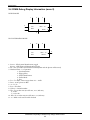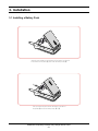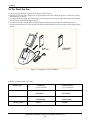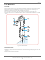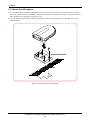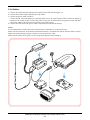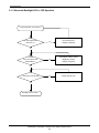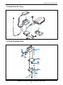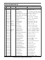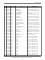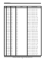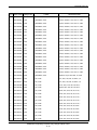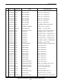
1
CDMA Cellular Phone
SCH-A105
SERVICE
Manual
CDMA Cellular Phone
CONTENTS
1. General Introduction
2. Specification
3. Installation
4. NAM Programming
5. Product Support Tools
6. Troubleshooting
7. Exploded view and its Part List
OK/
MENU
8. Electrical Parts List
‘
1.
4
7
3
2
6
5
8
0
9. Block diagram
9
10. PCB diagrams
11. Circuit diagrams
ELECTRONICS
©Samsung Electronics Co.,Ltd. July. 2000
Printed in Korea.
Code No.: GH68-01246A
BASIC.
1. General Description
The SCH-A105 cellular phone functions as both analog cellular phone working in AMPS (Advanced Mobile
Phone Service) mode and digital cellular phone working in CDMA (Code Division Multiple Access) mode.
CDMA type digital mode applies DSSS (Direct Sequential Spread Spectrum) mode which first came to be used
in the military.
The DSSS reduces channel cross talk and allow to use one frequency channel by multiple users in the same
specific area, resulting in increase of channel capacity to about ten times compared to that of analog mode
currently used.
Soft/Softer Handoff, Hard Handoff, and Dynamic RF Power Control technologies are combined into this phone
to reduce the call drop while usage.
CDMA digital cellular network consists of MSO (Mobile Switching Office), BSC (Base Station Controller),
BTS(Base Station Transmission System), and MS (Mobile Station). MS meets the specifications of the below:
• IS-95A : Mobile Station-Base Station Compatibility Standard for Dual-Mode Wideband Spread Spectrum
Cellular System
• IS-96A : Speech Service Option 1 Standard for Dual-Mode Wideband Spread Spectrum Cellular System
• IS-98A : Standards for Dual-Mode Wideband Spread Spectrum Cellular Mobile Station
• IS-126 : Mobile Station Loopback Service Options Standard
SAMSUNG Proprietary-Contents may change without notice
1-1
2. Specification
2-1 General
Frequency Range
Transmitter
Receiver
Digital Mode
: 824.64 ~ 848.37 MHz
: 869.64 ~ 894.37 MHz
Analog Mode
824 ~ 849 MHz
869 ~ 894 MHz
Channel Spacing
: 1.23 MHz
Number of Channels
: 20 EA
Duplex Spacing
: 45 MHz
Frequency Stability
: ±2.5 ppm (-20˚C ~ +50˚C, -4˚F ~ +122˚F)
Operating Temperature
: -20˚C~+50˚C (-4˚F ~ +122˚F)
Operating Voltage
HHP : 3.6V DC (±10%)
Hands-free : 13.7V DC (±10%)
Item
Size (mm)
30 kHz
832 CHs
45 MHz
Weight (g)
Including slim battery
80 x 42 x 22
93
Including standard battery
80 x 42 x 24
116
Operating Time
(Digital Mode)
Item
Standby Time
Talk Time
Slim battery
up to 100 hours
up to 150 min
Standard battery
up to 170 hours
up to 250 min
SAMSUNG Proprietary-Contents may change without notice
2-1
Specification
2-2 Digital Mode
Waveform Quality
0.944 or more
Time Reference
±1uS or less
Rx Sensitivity and Dynamic Range
Tx Output Power
-104 dBm, FER=0.5 % or less
-25 dBm, FER=0.5 % or less
280 mW (24.5 dBm)
Tx Frequency Deviation
±300 Hz or less
Occupied Band Width
1.32 MHz
Tx Conducted Spurious Emission
Minimum Tx Power Control
Open Loop Power Control
Standby Output Power
900 kHz : -42 dBc / 30 kHz below
1.98 MHz: -54 dBc / 30 kHz below
below -50 dBm
-25 dBm: -57.0 dBm ~ -38.5 dBm
-65 dBm: -17.5 dBm ~ + 1.5 dBm
-104 dBm: +18.0 dBm ~ +30.0 dBm
below -61 dBm
Closed Loop Tx Power Control Range
Test1: ±24 dB or less
Test2: 0 mS ~ 2.5 mS
Test3: ±24 dB or more
Test4: ±24 dB or more
Test5: ±24 dB or more
SAMSUNG Proprietary-Contents may change without notice
2-2
Specification
2-3 ANALOG MODE
TRANSMITTER
0.6W (+2/-4dB)
RF output power
Carrier ON/OFF conditions
“ON” Condition
“OFF” Condition
Compressor
Compression Rate
Attack Time
Recovery Time
Reference Input
within ±3dB of specification output (in 2mS)
below-60dBm (in 2mS)
2:1
3mS
13.5mS
Input level for producing a nominal ±2.9KHz
peak freqency deviation of transmitted carrier
6dB/OCT within 0.3 ~ 3KHz
Preamphasis
Maximum Freqency Deviation
F3 of G3
Supervisory Audio Tone
Signaling Tone
Wideband Data
Post Deviation Limiter Filter
3.0 ~ 5.9KHz
5.9 ~ 6.1KHz
6.1 ~ 15KHz
Over 15KHz
±12KHz
±2KHz (±10%)
±8KHz (±10%)
±8KHz (±10%)
above 40 LOG (F/3000) dB
above 35 dB
above 40 LOG (F/3000) dB
above 28 dB
Spectrum Noise Suppression
For all modulation
f0+20KHz ~ f0+45KHz
For modulation by voice and SAT
f0 +45KHz
For modulation by WBD(without SAT)
and ST (with SAT)
f0+45KHz ~ f0+60KHz
f0+60KHz ~ f0+90KHz
f0+90KHz ~ 2f0
Harmonic and conducted Spurious Emissions
above 26 dB
above 63 +10 LOG (PY) dB
above 45 dB
above 65 dB
above 63 +10 LOG (PY) dB
(where f0=carrier frequency
PY=mean output power in watts)
below 43 + 10 LOG (PY) dB
SAMSUNG Proprietary-Contents may change without notice
2-3
Specification
RECEIVER
-6dB / OCT within 0.3 ~3KHz
De-Emphasis
Expander
Expander Rate
Attack Time
Recovery Time
Reference Input
1:2
within 3mS
within 13.5mS
output level to a 1000Hz tone from a carrier
within ±2.9KHz peak frequency deviation
12dB SINAD / -116dBm
Sensitivity
Intermodulation Spurious Response Attenuation
avove 65dB
RSSI Range
above 60dB
Protection Against Spurious Response
Interference
above 60dB
In Band Conducted Spurious Emission
Transmit Band
Receive Band
Other Band
below -60dBm
below -80dBm
below -47dBm
Radiated Spurious Emission
Frequency Range
25 ~ 70 MHz
70 ~ 130MHz
130 ~ 174 MHz
174 ~ 260 MHz
260 ~ 470 MHz
470 ~ 1GHz
Maximum Allowable EIRP
-45dBm
-41dBm
-41 ~ -32dBm
-32dBm
-32 ~ -26dBm
-21dBm
SAMSUNG Proprietary-Contents may change without notice
2-4
Specification
2-4 CDMA Debug Display Information (menu 8)
IN IDLE MODE
1
2
3
SIx
Sxxxx
4
T-xx
x
Dxxx
Pxxx
-xx
6
CHxxx
8
7
5
IN CONVERSATION MODE
9
10
TEx
T-xx
Pxxx
REx
11
xx
Dxxx
x
-xx
3
CHxxxx
1 : Sxxxxx : SID (System ldentification) toggle
Nxxxxx : NID (Network Identification) toggle
2 : SIx : Slot cycle index (lowest between the system and the phone will be used)
3 : Handset Status : 0 - Acquisition
1 - Synchronization
2 - Paging (Idle)
3 - Traffic Initialization
4 - Traffic Mode
5 - Exit
4 : T-xx : Tx adjust, Value ranges from +63 ~ -63dB
5 : Dxxx : sector power in dBm
6 : -xx : Ec/Io
7 : Pxxx : PN offset
8 : CHxxxx : channel number
9 : TEx : Tx vocoder rate (8 is full rate, 1 is 1/8th rate)
E : EVRC
V : 13k or 8k
10 : REx : Rx vocoder rate (8 is full rate, 1 is 1/8th rate)
11 : xx : Walsh code used in traffic channel
SAMSUNG Proprietary-Contents may change without notice
2-5
3. Installation
3-1 Installing a Battery Pack
➀
➁
Insert the saw-toothed end on the bottom of the battery into the slots
on the bottom of the phone (➀), then slide the battery down (➁).
➂
➀
➁
Push up and hold the catch above the battery on the back of
the phone (➀) and lift the battery away. (➁ ~ ➂)
SAMSUNG Proprietary-Contents may change without notice
3-1
Installation
3-2 For Desk Top Use
1. Choose a proper location to install the charger for Desk Top use.
2. Plug the power cord of the charger into an appropriate wall socket. When the power is connected correctly,
the lamps turn on briefly.
3. To charge the battery pack, insert the battery pack into the rear slot of the charger. The lamp marked BAT on
the front panel of the charger lights up red.
4. If you do not wish to use the phone while charging the battery, insert the phone with the battery pack
attached into the front slot of the charger. The lamp marked PHONE on the front panel of the charger lights
up red.
SLIM
BATTERY
STANDARD
BATTERY
Figure 3-1 Charging the Phone and Battery
SPECIFICATIONS USING “DTCA10”
Battery Type
Model Name
SEC Code
Charging Time
Slim Battery
Standard Battery
(Li-ion, 500 mAh)
(Li-ion, 1000 mAh)
BTIA10AA
BTSA10AA
BTIA10AD
BTSA10AD
GH43-00173B
GH43-00174B
GH43-00179B
GH43-00180B
4 hours
4 hours
SAMSUNG Proprietary-Contents may change without notice
3-2
Installation
3-3 For Mobile Mount
3-3-1 Cradle
1. Choose a location where it is easy to reach and does not interfere with the driver’s safe operation of the car.
2. Separate the two halves of the clamshell by removing the two large slotted screws. See the figure 3-2.
3. Drill holes and mount the lower half of the clamshell by using the screws.
4. Place the cradle onto the remaining half of the clamshell and assemble them by using the screws.
5. Reassemble the two halves of the clamshell together. Adjust the mounting angle and tighten the two slotted
screws.
Figure 3-2 Cradle Installation
3-3-2 Hands-Free Box
1. Drill holes in a proper location for the hands-free box, attach the mounting bracket by using the screws. See
the figure 3-3.
2. Install the hands-free box into the bracket.
SAMSUNG Proprietary-Contents may change without notice
3-3
Installation
3-3-3 Hands-Free Microphone
1. It is recommended to install the microphone where it is 30-45 cm (12-18inch away from the driver. Choose
the location where is least susceptible to interference caused by external noise sources, ie, adjacent windows,
radio speakers, etc. Normal place is the sun visor.
2. Once the microphone has been correctly positioned, connect the microphone wire to the MIC jack on the
hands-free box.
MOUNTING BRACKET
CAR
40
55
Figure 3-3 Hands-Free Box 1 Installation
SAMSUNG Proprietary-Contents may change without notice
3-4
Installation
3-3-4 Cables
1. Connect the cradle and the hands-free box with the data cable. See the figure 3-4.
2. Connect the antenna cable to the RF jack of the cradle.
3. Connect the power cable as follows:
Connect the red wire to the battery (+) terminal, black wire to the vehicle chassis. Then connect the battery (-)
terminal to the vehicle chassis. Connect the yellow wire to the switched side of the ignition switch, and then
connect the white to the stereo mute wire from your vehicle stereo.
4. Connect the other end of the power cable to the PWR jack of the hands-free box.
Notes:
It is recommended to connect the power cable directly to the battery to avoid power noise.
Make sure the connection, in the vehicle, between the battery (-) terminal and vehicle chassis is made correctly.
Make sure the fuse having a proper capacity is used on the power cable.
Make sure the cables do not pass over any sharp metal edge that may damage it.
SAMSUNG Proprietary-Contents may change without notice
3-5
4. NAM Programming
NAM features can be programmed as follows:
Notes:
- If you enter the NAM program mode, each item shows the currenly stored data. Go to the next item by
pressing OK/
.
- You can modify the data by entering a new data.
- If you enter a wrong digit, press CLR to delete the last digit. Press and hold CLR to delete all digits.
- To scroll items backwards or forwards, press the VOLUME button on the left side of the phone.
4-1 General Setup
LCD Display
Key in
47 869#08#9
NAM program
1:General
2:Setup NAM1
3:Setup NAM2
47 869#08#9
1
-selects NAM programming
-choose ‘GENERAL’
ESN
B0000000
Volume ▼
-Electronic Serial Number of the phone
CAI version
3
Volume ▼
-The version of Common Air Interface supported by
the mobile
VOC8/13/EVRC
SO_VOIC_13K
Volume ▼
SCM
01101010
Volume ▼
-Station Class Mark displays the power class(bit0~1),
transmission(bit2), slotted class(bit5), dual mode(bit6).
Lock Code
0000
(0000)
4-digit code
-Lock code, current ststus is displayed
to change, enter new code.
OK/
-stores it
<or>
-Slot mode. ‘Yes’ indicates the slot mode.
OK/
changes the status.
-stores it.
0-7
OK/
-Slot mode index. The higher, the longer sleeping time
to change, enter new one.
-stores it.
Pref NAM1...
Digital pref
OK/
-Preferred system selection for NAM1
changes the system.
-stores it.
Pref NAM2...
Digital pref
OK/
-Preferred system selection for NAM2
changes the system.
-stores it.
Slot Mode
Yes
Slot Index
2
Function
-evrc, voice08k, voice13k
SAMSUNG Proprietary-Contents may change without notice
4-1
NAM Programming
4-2 Setting Up NAM1
LCD Display
Key in
NAM Program
1:General
2:Setup NAM1
3:Setup NAM2
2
-Choose ‘Setup NAM1.’
Setup NAM1
1:Phone #
2:FM
3:CDMA
1
-Choose ‘Phone #’
Phone #
3003003000
Phone number
-CDMA current number is displayed.
to change, enter new one
-stores it.
Mobile ID #
3003003000
Phone number
OK/
-CDMA current number is displayed.
to change, enter new one
-stores it.
Setup NAM1
1:Phone #
2:FM
3:CDMA
2
-Choose ‘FM’
FM Home SID
20
ID number
System ID for home, current status is displayed.
- to change, enter new one.
- store it.
FM 1st Chn
Channel number
OK/
Current 1st paging channel.
- to change, enter new one.
- store it.
ID number
OK/
Acquisition system ID 1, Current status is displayed.
- to change, enter new one.
- store it.
ID number
Acquisition system ID 2, Current status is displayed.
- to change, enter new one.
- store it.
334
FM Acq SID1
20
FM Acq SID2
0
FM Acq SID3
OK/
OK/
OK/
ID number
0
OK/
Function
Acquisition system ID 3, Current status is displayed.
- to change, enter new one.
- store it.
SAMSUNG Proprietary-Contents may change without notice
4-2
NAM Programming
LCD Display
Key in
FM Acq SID4
ID number
Acquisition system ID 4, Current status is displayed.
OK/
- to change, enter new one.
- store it.
ID number
Acquisition system ID 5, Current status is displayed.
OK/
- to change, enter new one.
- store it.
ID number
Acquisition system ID 6, Current status is displayed.
OK/
- to change, enter new one.
- store it.
ID number
Lock system ID 1, current status is displayed.
OK/
- to change, enter new one.
- store it.
ID number
Lock system ID 2, current status is displayed.
OK/
- to change, enter new one.
- store it.
ID number
Lock system ID 3, current status is displayed.
OK/
- to change, enter new one.
- store it.
ID number
Lock system ID 4, current status is displayed.
OK/
- to change, enter new one.
- store it.
ID number
Lock system ID 5, current status is displayed.
OK/
- to change, enter new one.
- store it.
ID number
Lock system ID 6, current status is displayed.
OK/
- to change, enter new one.
- store it.
ID number
Lock system ID 6, current status is displayed.
OK/
- to change, enter new one.
- store it.
* or #
FM Registration, current status is displayed.
OK/
- changes the status
‘YES’ to enable, ‘NO’ to disable
- store it.
0
FM Acq SID5
0
FM Acq SID6
0
FM LockSID 1
0
FM LockSID 2
0
FM LockSID 3
0
FM LockSID 4
0
FM LockSID 5
0
FM LockSID 6
0
FM LockSID1
0
Auto Reg
Yes
Function
SAMSUNG Proprietary-Contents may change without notice
4-3
NAM Programming
LCD Display
Key in
FM pref.
* or #
Preferred system selection, current status is displayed.
OK/
- changes the status
‘YES’ to enable, ‘NO’ to disable
- store it.
* or #
Current Access Overload Class.
OK/
- change the status.
- store it.
B pref
FM ACCOLC
0
Setup NAM1
1:Phone #
2.FM
3:CDMA
Function
- Choose ‘CDMA’
3
IMSI_MCC
number
000
IMSI_MNC
OK/
number
-IMSI Moble Country Code, current code is displayed.
to change, enter new one.
-stores it.
-IMSI Mobile Network Code, current code is displayed.
to change, enter new one.
-stores it.
00
OK/
B pref
<or>
OK/
-Preferred system selection, current system is displayed.
changes the system.
-stores it.
CDMA ACCOLC.
0
class number
CDMA Access Overload Class, current status is displayed.
-to change, enter new one.
-stores it.
Pchn Sys A
channel number
CDMA pref..
283
Pchn Sys B
OK/
OK/
channel number
384
Schn Sys A
OK/
channel number
691
Schn Sys B
OK/
channel number
777
OK/
-Preferred channel currently used under system A
to change, enter new one.
-stores it.
-Preferred channel currently used under system B
to change, enter new one.
-stores it.
-Second channel currently used under system A
to change, enter new one.
-stores it.
-Second channel currently used under system B
to change, enter new one.
-stores it.
SAMSUNG Proprietary-Contents may change without notice
4-4
NAM Programming
LCD Display
Key in
CD Acq SID 1
ID number 1~ 6
-1st Acquisition system ID, current status is displayed.
OK/
to change, enter new one.
-stores it.
ID number 1~ 6
-2nd Acquisition system ID, current status is displayed.
OK/
to change, enter new one.
-stores it.
ID number 1~ 6
-3rd Acquisition system ID, current status is displayed.
OK/
to change, enter new one.
-stores it.
ID number 1~ 6
-4th Acquisition system ID, current status is displayed.
OK/
to change, enter new one.
-stores it.
ID number 1~ 6
-5th Acquisition system ID, current status is displayed.
OK/
to change, enter new one.
-stores it.
ID number 1~ 6
-6th Acquisition system ID, current status is displayed.
OK/
to change, enter new one.
-stores it.
ID number
-1st lock system ID,current status is displayed.
OK/
to change, enter new one.
-stores it.
ID number
-2nd lock system ID,current status is displayed.
OK/
to change, enter new one.
-stores it.
ID number
-3rd lock system ID,current status is displayed.
OK/
to change, enter new one.
-stores it.
ID number
-4th lock system ID,current status is displayed.
OK/
to change, enter new one.
-stores it.
ID number
-5th lock system ID,current status is displayed.
OK/
to change, enter new one.
-stores it.
ID number
-6th lock system ID,current status is displayed.
OK/
to change, enter new one.
-stores it.
<or>
-CDMA Home system ID, current status is displayed
changes the status.
-stores it.
20
CD Acq SID 2
0
CD Acq SID 3
0
CD Acq SID 4
0
CD Acq SID 5
0
CD Acq SID 6
0
CD lockSID 1
0
CD lockSID 2
0
CD lockSID 3
0
CD lockSID 4
0
CD lockSID 5
0
CD lockSID 6
0
CDMA Home SID
Yes
OK/
Function
SAMSUNG Proprietary-Contents may change without notice
4-5
NAM Programming
LCD Display
Key in
CDMA fSID
<or>
-CDMA foreign SID, current status is displayed.
OK/
changes the system.
-stores it.
<or>
-CDMA foreign NID, current status is displayed.
OK/
changes the system.
-stores it.
number
-first SID written in the list, current status is displayed.
OK/
to change, enter new one.
-stores it.
number
-first NID written in the list, current status is displayed.
OK/
to change, enter new one.
-stores it.
number
-2nd SID written in the list, current status is displayed.
OK/
to change, enter new one.
-stores it.
number
-2nd NID written in the list, current status is displayed.
OK/
to change, enter new one.
-stores it.
number
-3rd SID written in the list, current status is displayed.
OK/
to change, enter new one.
-stores it.
number
-3rd NID written in the list, current status is displayed.
OK/
to change, enter new one.
-stores it.
number
-4th SID written in the list, current status is displayed.
OK/
to change, enter new one.
-stores it.
number
-4th NID written in the list, current status is displayed.
OK/
to change, enter new one.
-stores it.
Yes
CDMA fNID
Yes
SID #1
20
NID #1
65535
SID #2
20
NID #2
65535
SID #3
20
NID #3
65535
SID #4
20
NID #4
65535
Function
4-3 Setting Up NAM 2
LCD Display
Key in
NAM Program
1:General
2:Setup NAM1
3:Setup NAM2
3
Function
-Choose ‘Setup NAM2’
The NAM2 setup program is the same as ‘NAM1’
SAMSUNG Proprietary-Contents may change without notice
4-6
5. Product Support Tools
5-1 General
IMPORTANT INFORMATION
Purpose
The Product Support Tool (PST) offers you the ability to interface with the SAMSUNG CDMA telephone using
a PC. With this tool you can program the phones network system requirements and functionality, swap phone
data, and download software upgrades. This document supports UniPST version 1.xx.
NOTE: This software must be executed in the Windows95/98 mode.
EQUIPMENT REQUIRED
Make sure you have the following equipment setup:
1. Minimum PC configuration: 586 CPU, 16MB RAM, Windows95/98, 5MB of disk space free for software
upgrade.
2. PST Software with appropriate cable (DM Cable for SAMSUNG CDMA phone).
3. Serial Port (16550 Serial Interface Card).
4. Power Supply (3.8 V) or Battery
INSTALLATION
Software
1.Insert the PST floppy disk into drive (A:\).
2.Create an appropriate directory on the C:\ drive for PST software, Execute Setup.exe file,
The installation program creates folder and task bar on the windows95/98 start bar.
SAMSUNG CDMA Phone
The serial port should be configured to COM1 or COM2.
Use the following procedure to connect the phone, cable, and PC .
Plug the female end of the DM Cable into the 16550 card.
Pull the black rubber connector away from the socket at the base of the phone.
Plug the special connector on the cable into the socket at the base of the phone.
SAMSUNG Proprietary-Contents may change without notice
5-1
Product Support Tools
5-2. PST (Product Support Tool)
5-2-1 Getting Started
MAIN MENU SCREEN
1. At the Windows95/98, Double Click “UniPst.exe”.
2. The Main Menu Screen will be displayed.
The Main Menu Screen shows the basic tasks that are available.
CAUTION: DO NOT attempt to program phone with a low battery.
PST SETUP
UniPst supports SAMSUNG CDMA portable telephone. You can select serial port COM1 or COM2.
5-2-2 Operation Procedure
Service Programming
The Service Programming screens enable you to set and change the service activation parameters of the
phones. These items can be changed individually or as a group via the “Edit Items” Property Sheet of the PST.
There are several pages on the Service Programming Property Sheet (See below Figure).
Read Data from File
Click “open” icon to select the name of a file whose extension is “mmc”. The values will be read from the
named file, and will initialize the parameter values seen on the Service programming screen
Read Data from Phone
Click Read from the Phone icon to upload the current programmable parameters of the phone. The values are
read from the phone, so the phone must have the power ON and be properly connected to the PST.
NOTE: To actually view the data you need to go to the Edit Items screens.
Edit Items
Click this icon to edit Number Assignment Module (NAM) items or UI items.
There are two types of screens:
1. Parameters associated with a particular Number Assignment Module (NAM)
2. UI items settings
Phone Book
Click this icon to edit Phone Book.
While you edit cell, you can use <Enter> and < UP , DOWN,LEFT,LIGHT Arrow> and <SPACE> key. If you
want to edit phone number or name , you must move rectangle box to cell where you want to edit , Write it
down . if <UP and DOWN Arrow> key is pressed, the cursor moves to next cell or previous cell.
SAMSUNG Proprietary-Contents may change without notice
5-2
Product Support Tools
Save Data to File
Click this icon to save the current parameters to a file. Once you enter a filename, Click <OK> button to write
all current parameters to that file. This way the same information can be downloaded into multiple phones.
Write to Phone
Click this icon to write the selected parameter values to the phone. Writing the selected values to the phone
may take up to a minute.
If there are dependencies in a field you can make all the changes in the proper fields and download the
information all together.
If you intend to use this “Write to Phone” feature, it is recommended that you do a “Read Data from Phone”
first, and then make the changes, so that nothing gets inadvertently overwritten.
NOTE: DO NOT TOUCH THE PHONE WHILE WRITING IS IN PROGRESS.
Software Download and Upgrade Screen
To begin a software upgrade or download, perform the following steps:
1. From the main menu screen choose DOWNLOAD MODE?
Click open icon to choose a BIN file of the new software to be loaded. Choose the appropriate BIN file, then
Click <Open> (see below figure).
2. Click Download? to begin downloading the file. You will notice various messages and a progress bar that
informs the user what percentage of the downloading has already occurred.
3.Click Mode Select box, then Select SERVICE MODE?to return to the Service Mode Screen.
NOTE: DO NOT POWER OFF WHILE THE PHONE IS BEING DOWNLOADED!
SAMSUNG Proprietary-Contents may change without notice
5-3
Product Support Tools
5-3 TEST PROCEDURE
5-3-1 Configuration of Test
Spectrum Analyzer
RF In
HP8924C
RF
In/Out
Audio Audio
Out
In
Directional
Coupler
To A-Out
Test Jig
To A-In
DC Power Supply
(+3.93V)
❈ CAUTION : Because there is the loss (0.33V at Max Power) of the test jig and Data cable, you’d better input
3.93V to the DC Power Supply to use 3.6V (Battery normal voltage) at Cellular phone
Items needed to purchase from SAMSUNG
ITEMS
PARTS #
RF Cable
Test cable
DM Cable
Test JIG
(RF Interface Pack Ass’y)
GH39-00026A
GH39-00028A
GH39-30525A
GH80-00001A
REMARK
Including
1. Power Cable(Black,Red)
2. 9-pin RS232 data Cable
SAMSUNG Proprietary-Contents may change without notice
5-4
Product Support Tools
5-3-2 List of Equipment
- DC Power Supply
- Test Jig
- Test Cable
- CDMA Mobile Station Test Set
- Spectrum Analyzer(include CDMA Test Mode)
HP8924C, HP83236A, CMD-80, etc
HP8596E
TEST JIG
AUDIO SELECT
LEFT: AUDIO IN
RIGHT: AUDIONOFF
DC POWER INPUT PORT
CHANGE VOLTAGE LEVEL
BY MODEL (3.8VDC)
RED: +
BLACK: GND
UP: AUTO POWER ON
DOWN: NOT USE
AUTO
DB25 CONNECTOR
CPMMECT TO
DB25 CONNECTOR
OF TEST CABLE
A-IN
- DC3.8v +
D89 CONNECTOR
CONNECT TO IBM
PC SERIAL PORT
TO_PC
T
E
S
T
HHP I/F TEST JIG
P
A
C
K
BJ11 CONNECTOR
CONNECT TO HP
SERIAL PORT
TO_HP
TO
A-OUT
TO
A-IN
PROBE
NOT USED
CONNECT TO
AUDIO OUT PORT OF
TEST EQUIPMENT
(USE BNC CABLE)
CONNECT TO
AUDIO IN PORT OF
TEST EQUIPMENT
(USE BNC CABLE)
TEST CABLE
2
3
1
4
5
6
SAMSUNG Proprietary-Contents may change without notice
5-5
Product Support Tools
TEST CABLE CONNECTIONS
1
MHC 172
2
RF CABLE (1.4 dB Loss)
3
BNC CONNECTOR (RF)
4
PLUG CONNECT TO SCH-A105
5
DATA CABLE
6
Dsub 25PIN CONNECTOR (DATA)
Dsub 25 PIN CONNECTOR PIN DESCRIPTION (TEST CABLE 1, BACK SIDE)
DATA DESCRIPTION
Dsub CONN.
PIN NO.
DATA DESCRIPTION
Dsub CONN.
PIN NO.
V_F
12,21
DP_RX_DATA
8
DGND
2,4,6,13,19
HP_PWR
9
BATT
15,16,22
RI
10
C_F
3,20
CD
11
TX_AUDIO
5
RTS
14
DP_TX_DATA
7
CTS
17
RX_AUDIO
1
DTR
18
15
14
1
17
16
2
3
19
18
4
5
21
20
6
7
23
22
8
9
25
24
10
11
SAMSUNG Proprietary-Contents may change without notice
5-6
12
13
Product Support Tools
5-4. CONVERSION TABLE OF FREQUENCY vs CHANNEL
TYPE
CHANNEL
CONVERSION EQUATION
REMARK
TX
1 ≤ N≤ 799
F=0.03 ✕ N + 825.00
FREQUENCY
990 ≤N≤1023
F=0.03 ✕ (N-1023) + 825.00
N ; CH NUMBER
RX
1 ≤N≤ 799
F=0.03 ✕ N + 870.00
F ; FREQUENCY
FREQUENCY
990 ≤N≤1023
F=0.03 ✕ (N-1023) + 870.00
Change to Test Mode
A. To change the phone’s state from Normal Mode to Test Mode, You should enter the following keys.
“*759#813580“
B. The command “0 1” is Suspend.
C. To finish the Test Mode, You should enter the command “0 2”.
* Note: Make sure to change to “Digital only” or “Analog only” mode in NAM1,
EST MODE. (Refer to 4. NAM Programming)
Channel Selection and Tx Power Output Level Control
1. Digital Mode (CDMA)
A. Enter to Test Mode ( * 7 5 9 # 8 1 3 5 8 0 ).
B. “0 1” : Suspend.
C. “0 9 0 3 6 3 #” : Set to ‘0363’ channel.
D. “0 7” : Carrier On.
E. “3 4” : Spread spectrum to 1.23MHz band width.
F. “7 1 2 7 5 #” : Output RF power level setting.
“275” means AGC level and AGC level range is from 0 to 511.
2. Analog Mode ( FM )
A. Enter to Test Mode ( * 7 5 9 # 8 1 3 5 8 0 ).
B. “0 1” : Suspend.
C. “4 6” : Vocoder initial to Analog mode.
D. “0 9 0 3 8 3 #” : Set to ‘0383’ channel.
E. “0 7” : Carrier On.
F. “7 2 2 7 5 #” : Output RF power level setting.
“275” means AGC level and AGC level range is from 0 to 511.
G. “1 0 2” : RF Power level control, 2(0~7) means power level .
SAMSUNG Proprietary-Contents may change without notice
5-7
Product Support Tools
5-5 TEST COMMAND TABLE
Command No.
Signal. Name
Description
1
SUSPEND
enter to test menu
2
RESTART
escape from test menu
3
SAVE_VAL
Save values in e2prom only in auto test
4
GET_MODE
Get mode CDMAFM AUTO TEST
5
SET_MODE
Set mode CDMAFM AUTO TEST
6
WRITE_NV
Write the EEPROM item
7
CARRIERON
turn on the carrier
8
CARRIEROFF
turn off the carrier
9
LOADSYN
load the synthesizer for locking
10
PWRLEVEL
change RF power level
11
RXMUTE
mute rx audio
12
RXUNMUTE
unmute rx audio
13
RXMUTE
mute tx audio
14
TXUNMUTE
unmute tx audio
15
VOC_ESEC
Echo Canceller
16
STON
turn on ST
17
STOFF
turn off ST
18
LCD_CONTRAST
index up key JOJ_98.11.23(contrast)
19
INDEX_DECR
index dn key JOJ_98.07.07
20
LNA_GAIN_WR
22
SNDNAM
Send NAM Information
23
SNDVERSION
Send Software Version
24
SNDESN
Send ESN
25
BACKLIGHT_ON
Backlight on
26
BACKLIGHT_OFF
Backlight off
27
LAMP_ON
LAMP on
28
LAMP_OFF
LAMP off
29
REBUILD
Rebuilding EEPROM
30
SPC
-
-
31
PLINE
Product lile information
32
SATON
turn on SAT
33
SATOFF
turn off SAT
34
CDATA
continuously sen TX Control data
35
VOLUME_UP
Electric Volume Up
36
VOLUME_DOWN
Electric Volume Down
SAMSUNG Proprietary-Contents may change without notice
5-8
Product Support Tools
Command No.
Signal. Name
Description
38
VOC_ENC_OFFSET
Vocoder ENC offset
39
VOC_DEC_OFFSET
Vocoder DEC offset
40
VOC_CDMA_UNITY_GAIN
Vocoder CDMA unity gain
41
VOC_FM_HFRX_UPGAIN
Vocoder fm hfrx upgain
42
DTMFON
turn on DTMF
43
DTMFOFF
turn off DTMF
44
COMPANDORON
turn on compandor
45
COMPANDOROFF
turn off compandor
47
FM_AUD_GAIN
FM audio gain
48
VIBRATOR_ON
activate a vibrator
49
VIBRATOR_OFF
inactivate a vibrator
50
BATT_TYPE
Battery Type
51
BBA
BBASIC supplier
52
HW_VERSION
HW version hmk_96.12.09
53
CARRIER
Target Carrier option
54
VOC13K
Target Service option
55
EXT_AUDIO
External Audio Path OnOff
56
LOOP_BACK
Loop back on
57
MIC_ON
mute MIC Path
58
MIC_OFF
unmute MIC Path
59
ALLPATH
tune on the all audio path
60
FM_TX_GAIN
61
FM_RX_GAIN
62
DTMF_VOL_TX
63
TX_LIMITER
64
FM_SAT_LEVEL
65
FM_FREQ_SGAIN
66
FM_ST_GAIN
67
READ_BATT
Saved Low battery value read
68
VBATT1
set the low battery position in the standby
69
VBATT2
set the low battery position in the talking
70
WRITE_BATT
write a BATT
71
CDMA_TXADJ
sets tx_agc_adj for cdma mode
72
FM_TXADJ
sets tx_agc_adj for fm mode
73
SET_PA_RO
set TX power AMP ctrl RO JOJ_98.06.29
74
OFF_PA_RO
off TX power AMP ctrl RO JOJ_98.06.29
READ_RSSI
read a RSSI
-
-
75
SAMSUNG Proprietary-Contents may change without notice
5-9
Product Support Tools
Command No.
Signal. Name
Description
76
WRITE_RSSI
write a RSSI
77
READ_TEMP
read a TEMP
78
RXRAS_AUTO
adj RXRAS from 8924C JOJ_98.06.20
79
BUZZER_ON
Buzzer on
80
BUZZER_OFF
Buzzer off
81
VOC_PCMLPON
turn on to play a PCM LOOP BACK
82
VOC_PCMLPOFF
turn off to play a PCM LOOP BACK
83
DATASVC_ON
rsm_ifc data svc
84
DATASVC_OFF
rsm_ifc data svc
85
SPEAKER_ON
turn on the speaker path
86
SPEAKER_OFF
turn off the speaker path
87
FM_LOOP_TEST
FM loop back
88
TRK_ADJ
TRK LOCAL ADJUST
89
CDTRK_ADJ
CDMA TRK LOCAL ADJUST
90
EVRC_TEST
EVRC Check Mode kjg_980417_evrc
91
SVC_LED
SVC_LED control hjkim_990113
92
TXRAS_ADJ
TX RAS adj = TXRAS offset arry
93
RXRAS_ADJ
RX RAS adj = RXRAS offset arry
94
HW_CHANFLAT
95
SW_CHANFLAT
96
CH_FLATNESS
97
FM_TX_PWR
99
TEMP
100
MAX
-
-
setting the volume for power Level 2-7
SAMSUNG Proprietary-Contents may change without notice
5-10
6. Troubleshooting
6-1 Logic Section
6-1-1 Power Failure
Press & hold END/
button
Q110 Drain=‘H’?
No
Check the signal path from the battery
terminal to Q110 source, R185,
R115 & Q102.
Yes
Check U105, R188, C165 & R112
and its neighboring circuits.
No
Check Q104 and its neighboring
circuits.
No
Check U201 and its neighboring
circuits.
Yes
U104 pin9p=‘H’?
No
Q104 collector=‘L’?
Yes
U201 pin 1 output
=3.0V?
Yes
END
SAMSUNG Proprietary-Contents may change without notice
6-1
Troubleshooting
6-1-2 Abnormal Initial Operation (Normal +3.3V source)
Press END/
button
TCXO CLK
applied to U401 pin 36&
U501 pin35?
No
Check TCXO output,
R310 and C325.
Replace if required.
No
Check U401 and its meighboring
circuit. Replace if required.
No
Check ‘H’ level input from
U101 pin P6 and U401 pin79.
No
Check the LED and its neighboring
circuit. Replace if required.
No
Check the LCD pins and its
neighboring circuit.
Replace if required.
Yes
TCXO CLK signal output
from U401 pin 37?
Yes
CHIPX8 CLK signal output
from U401 pin 38?
Yes
LED ON?
Yes
Normal initial
display on LCD?
Yes
END
SAMSUNG Proprietary-Contents may change without notice
6-2
Troubleshooting
6-1-3 Abnormal Backlight,LCD or LED Operation
Press and button on the phone
‘H’ level output from
U104 pin 7L?
No
Check U104 pin7L
Replace if required
No
Check Q108 & Q107 and its
neighboring circuits.
Replace if required
No
Check U104 pin 13p
Yes
‘H’ level
from U101 pin7L drive
Q108 & Q107?
Yes
‘L’ level from U104 pin13p?
Yes
Backligh LED or LCD on
SAMSUNG Proprietary-Contents may change without notice
6-3
Troubleshooting
6-1-4 Abnormal Key Data Input
Check initial status
Scanning signals
output from U104 pins 4A,
4B,5A,5C,5D,6C,
5E.?
No
Check U104 pins
4A,4B,5A,5C,5D,6C,5E
No
Replace the keypad assembly
Yes
Check U104 pin 2A,4C, and 3B
Yes
Check CON J1.
Yes
Normal key data input?
Yes
END
SAMSUNG Proprietary-Contents may change without notice
6-4
Troubleshooting
6-1-5 Abnormal Key Tone
Check initial status
Scanning signals
ouput from U104 pins
4A,4B,5A,5C,5D,6C,
5E.?
No
Check U104 pins
4A,4B,5A,5C,5D,6C,5E.
No
Replace the Keypad assembly.
Yes
Check U104
pins 2A,4C and 3B.
Yes
Check CON J1.
Yes
Normal Key data input?
Yes
END
SAMSUNG Proprietary-Contents may change without notice
6-5
Troubleshooting
6-2 Transmitter Section
Abormal
transmitter
section
No
Check TX
PLL OK?
No
Yes
Check U303
Pin2?
YES
Check
OSC300?
Pin1
969.96 MHz
CH:486
Tcxo:19.68 MHz
Yes
Check TX
Power level.
OK?
No
Check U304
Tx IF Level?
Yes
Gain: -15 dBm
No
Check
U504 Local Input
Level?
Yes
Check Q503
Level?
CDMA:0 dBm
Gain: 0 dBm
No
Yes
Gain: + 20 dB
No
SAMSUNG Proprietary-Contents may change without notice
6-6
Check U304
Tx IF Level?
Gain: + 28 dB
Troubleshooting
6-3 Receiver Section
RX part
No
Check CDMA
SVC&ROAM?
Check LNA
in/output OK?
No
Check Duplexer
& LNA power
Gain: +18 dB
Yes
Yes
Yes
Check 1st
local & mixer power
OK?
Check mixer
in/output OK?
Gain: -11 dB
No
Check PLL (U407)
& VCO output
local: - 5 dBm
BUFFER OUTPUT: - 5 dBm
Yes
Check IF AMP
in/output OK?
No
Check IF AMP
power OK?
Gain: +19 dB
Yes
Check IF filter
in/output OK?
No
Check IF filter
solderling
Loss: -10 dB
Yes
RF Rx FM OK
BBA INPUT: -52 dBm
SAMSUNG Proprietary-Contents may change without notice
6-7
Troubleshooting
6-4 RF Section
Start CDMA mode
Normal CDMA
SVC & ROAM OK?
No
Check CDMA RX path
No
Check Transmitter
Yes
Setup CDMA
call. OK?
No
Yes
Measure
CDMA FER
Yes
Normal CDMA RF?
SAMSUNG Proprietary-Contents may change without notice
6-8
7. Exploded View and its Parts List
7-1 Cellular phone Exploded View
2-1
2-2
2-3
6-3
6-2
6-1
SAMSUNG Proprietary-Contents may change without notice
7-1
Exploded view and its Part List
SEC.CODE
No
Description
1
2
REMARK
Silver Gray
Champagne Gold
SUA, FOLDER REAR
GH75-00148M
GH75-00148L
LCD MODULE
GH96-00869A
GH96-00869A
2-1
BUZZER
3002-001062
3002-001062
2-2
SPEAKER
3001-001103
3001-001103
2-3
VIBRATOR
3101-001169
3101-001169
3
SUA, FOLDER FRONT COVER
GH97-01592B
GH97-01592A
4
SCREW MACHINE
6001-000464
6001-000464
5
LCD WINDOW
GH72-01045A
GH72-01045A
6
KEY PCB
GH59-00085A
GH59-00085A
6-1
MIC
3003-001034
3003-001034
6-2
METAL DOME SHEET
GH74-00456A
GH74-00456A
6-3
REED SWITCH
3409-001039
3409-001039
7
MAIN PBA
GH92-00824A
GH92-00824A
8
BATTERY
GH43-00179B
GH43-00173B
500 mAh
GH43-00180B
GH43-00174B
1000 mAh
9
SCREW MACHINE
6001-001057
6001-001057
10
SUA, REAR COVER
GH75-00149B
GH75-00149A
11
ANTENNA
GH42-00015B
GH42-00015B
12
KEY PAD
GH73-00085F
GH73-00085F
13
VOLUME KEY
GH72-00300C
GH72-00300C
14
EAR JACK COVER
GH72-00301A
GH72-00301A
15
SUA, FRONT CASE
GH75-00525B
GH75-00525A
16
RF JACK DUMMY
GH73-00083A
GH73-00083A
SAMSUNG Proprietary-Contents may change without notice
7-2
Exploded view and its Part List
7-2 Desk-Top Rapid Charger Ass’y
A
TYPE
7-3 Travel Charger Ass’y
SEC. CODE
Remark
A
GH44-00104D
Brazil
B
GH44-00104C
Mexico
(TC010, GH44-00080B)
7-4 Cigarette Lighter Adaptor Ass’y
B
(CLC020, GH44-00070A)
SAMSUNG Proprietary-Contents may change without notice
7-3
Exploded view and its Part List
7-5 Hands Free Kit Ass’y
7-6 Cradle Exploded View
SAMSUNG Proprietary-Contents may change without notice
7-4
8.ElectricalPartsList
Level
SEC CODE Design LOC
ITEMS
DESCRIPTIONS
0
SCH-A105G/TCL
1
3001-001103
SPEAKER
0.05W, 32ohm, 111dB, -
1
3003-001034
MIC-CONDENSOR
2V, 130UA-500UA, -44DB+-3DB, 2.2KOHM
1
GH42-00015B
ANTENNA-SCHA100
SCH-A100, 824-849MHz, 0/-3DBD, 50OHM
1
GH43-00173B
BATTERY-500mA, L/GRY, ISR, MAIN
3.7V, 540mAh, -, 540mA, 4.2V
1
GH43-00174B
BATTERY-1000M, L/GRY, ISR, MAIN
3.6V, 915mAH, -, 965mAH, -
1
GH44-00104D
CHARGER-DTCA101
SCH-A101, AC/DC, -, 110-220VAC
1
GH82-00008A
A/SMATERIALASSY-SCHA100
SCH-A100, -, KOR, SVCPBAASS’Y, -, -,
2
3001-001103
SPEAKER
0.05W, 32ohm, 111dB, -
2
3002-001062
BUZZER-MAGNETIC
88dB, 3.6V, 90mA, 2.731KHz, TP
2
3003-001034
MIC-CONDENSOR
2V, 130UA-500UA, -44DB+-3DB,
2
3101-001169
MOTOR
MOTOR-DC
8500rpm, -, 3V, 110mA
2
3409-001039
REEDSWITCH SWITCH-REED
2
6001-000464
SCREW-MACHINE
PH, +, M1.4, L4, BLACK, SM10C, -
2
6001-001057
SCREW-MACHINE
PH, +, M1.4, L6, ZPC(BLK), MSWR20,
2
GH39-00026A RFCABLE
CBFSIGNAL-SCHA100
SCH-A100, -, RFTESTCABLE, 1800+-20,
2
GH42-00015B ANT
ANTENNA-SCHA100
SCH-A100, 824-849MHz, 0/-3DBD,
2
GH68-00370A
LABEL(R)-FRONTDUMMYSHEET
SCH-A100, PCSHEET, PI4.4, T0.3,
2
GH72-00300C
PMO-VOLUMEKEY
SCH-A100, PC, GRY, -, -
2
GH72-00301A
PMO-EARJACKCOVER
SCH-A100, PUR, L/GRY, -, -
2
GH72-01045A
PMO-LCDWINDOW(SVC)
SCH-A101, ACRYL, BLK, -, -
2
GH73-00083A
RMO-RFJACKDUMMY
SCH-A100, RUBBER, -, GRY, 50
2
GH73-00085F
RMO-KEYPAD
SCH-A100, RUBBER, -, -, -
2
GH74-00456A
MPR-METALDOMESHEET
SCH-A101, PETFILM+SUS301, T0.07, -, -
2
GH75-00148L
MEC-FOLDERREAR
SCH-A100, -, BEG
3
GH71-00049G
NPR-DECORATIONPANNEL
SCH-A100, AL, T0.6, GLD
3
GH72-00293A
PMO-REARFOLDER
SCH-A100, PC, BEG, -, -
3
GH74-00138A
MPR-DECO.PANNELTAPE
SCH-A100, TESA, T0.2, TRP, -
3
GH74-00151A
MPR-DECOPANNALBOHOTAPE
SCH-A100, VINYL, T0.2, -, -
2
GH75-00525A
MEC-SUA.FRONT
SCH-A101(ISRL), -, BEG
3
GH72-00286A
PMO-FRONTCOVER
SCH-A100, PC, BEG, -, -
3
GH72-00287A
PMO-LEDLENS
SCH-A100, ACRYL, TRP, -, -
3
GH72-00295A
PMO-HINGEDUMMY
SCH-A100, POM, BLK, -, -
3
GH73-00263A
RMO-FOLDHOLDER
SGH-A100, RUBBER, -, D/GRY, -
BUZZER
100VDC, 0.5A, 1000US, 1000US
SAMSUNGProprietary-Contentsmaychangewithoutnotice
8-1
Electrical Parts List
Level
SEC CODE Design LOC
ITEMS
DESCRIPTIONS
2
GH97-00925D
MEAREAR-COVER
SCH-A101, -, ISRL, GRY, -, -, -
3
GH71-00050A
NPR-ANTENNABRAKET
SCH-A100, ZNGOLDPLT, -, AU
3
GH71-10639A
NPR-SHIELDSTRIP(A)
SCH-1100, C1720S-1/2H, T0.1, GOLD
3
GH75-00149A
MEC-SUA.REARCOVER
SCH-A100, -, GRY
4
GH68-00389A
LABEL(R)-DUPLEXDUMMY
SCH-A100, MAT, 22X11, T0.05, GRY
4
GH70-10633A
IPR-LOCKERSPRING
SCH-750, STS304, T0.3, -
4
GH72-00298A
PMO-REARCOVER
SCH-A100, PC, GRY, -, -
4
GH72-00299A
PMO-LOCKER
SCH-A100, PC, GRY, -, G5295
2
GH97-01591A
MEAETC-KEYFPCB
SCH-A101, -, ISRL, WHT, -, -, -
3
GH59-00085A KEYPADASS’Y UNIT-SCHA101KEYPAD
SCH-A101, KBSCHA101, KEYPADASS’Y, -
3
GH71-00207A
NPR-SOLDERFINGER
SCH-A120, C5210TS, T0.15, AU
3
GH72-00294A
PMO-SHIELDCOVER
SCH-A100, ABS, BLK, -, -
2
GH97-01592A
MEAETC-FOLDERFRONT
SCH-A101, -, ISRL, BEG, -, -, -
3
GH72-00297B
PMO-LCDWINDOW
SCH-6900, ACRYL(T1), -, -, -
3
GH74-00152A
MPR-WINDOWBOHOTAPE
SCH-A100, VINYL, T0.2, -, -
3
GH74-00566A
MPR-SPEAKNET
SCH-A101, HIMERON, PI12.6XT1.65, -, -
3
GH75-00146D
MEC-FOLDERFRONT
SCH-A100, -, BEG
4
GH72-00288D
PMO-FOLDERFRONT
SCH-A100(ISRL), PC, BEG, -, -
4
GH72-00289A
PMO-EARPIECE
SCH-A100, PC, GRY, -, -
4
GH74-00135A
MPR-LCDWINDOWTAPE
SCH-A100, TESA, T0.2, TRP, -
4
GH74-00137A
MPR-EARPIECETAPE
SCH-A100, TESA, T0.2, TRP, -
4
GH74-00600A
MPR-LCDSPONGE
SCH-A101, SRSPORON, T0.5, BLK, -
4
GH75-00414B
MEC-HINGEASS’Y
SCH-850, -, BLK
5
GH70-00020A
IPR-SPRINGHINGE
SCH-A100, STS304, PI4.5XPI0.65X8.2, -
5
GH72-00291A
PMO-SHAFTHINGE
SCH-A100, POM, BLK, -, -
5
GH72-00292A
PMO-CAMHINGE
SCH-A100, POM, BLK, -, -
5
GH72-00861A
PMO-HINGEHOUSING
SCH-850, PC, SIL, -, -
3
GH75-00164A
MEC-MAGNETICHOLDER
SCH-A100, SEC, BLK
4
GH70-40005A
ICT-MAGNETIC
SPH-7000, MAGNETIC, 3x15XT1.0, -
4
GH72-00296A
PMO-MAGNETICHOLDER
SCH-A100, PC, BLK, -, -
4
GH74-00150A
MPR-TAPEMAGNETICHODER
SCH-A100, TESA, T0.2, TRP, -
1
GH92-00824A
PBAMAIN-IFC2
IFC2, -, KORA, MAINPBA, -, -, -
2
0405-001035
D402
DIODE-VARACTOR
1SV279, 15V, 3nA, USC, TP
2
0405-001035
D403
DIODE-VARACTOR
1SV279, 15V, 3nA, USC, TP
SAMSUNG Proprietary-Contents may change without notice
8-2
Electrical Parts List
Level
SEC CODE Design LOC
ITEMS
DESCRIPTIONS
2
0405-001035
D501
DIODE-VARACTOR
1SV279, 15V, 3nA, USC, TP
2
0405-001035
D502
DIODE-VARACTOR
1SV279, 15V, 3nA, USC, TP
2
0406-001051
ZD102
DIODE-TVS
SMS05C, 6V, 300W, SOT-23-6
2
0406-001051
ZD103
DIODE-TVS
SMS05C, 6V, 300W, SOT-23-6
2
0406-001084
ZD201
DIODE-TVS
SMF05, 6/-/V, 200W, -
2
0407-000115
D100
DIODE-ARRAY
DAN202U, 80V, 100mA, CA2-3, SC-70,
2
0407-000115
D202
DIODE-ARRAY
DAN202U, 80V, 100mA, CA2-3, SC-70,
2
0407-001006
D200
DIODE-ARRAY
DA221, 20V, 100mA, C2-3, EM3, TR
2
0407-001006
D201
DIODE-ARRAY
DA221, 20V, 100mA, C2-3, EM3, TR
2
0407-001006
D500
DIODE-ARRAY
DA221, 20V, 100mA, C2-3, EM3, TR
2
0409-001016
D401
DIODE-PIN
BAR63-02W, 50V, 100mA, SCD-80, TP
2
0501-000162
Q106
TR-SMALL SIGNAL
2SA1576, PNP, 200mW, SOT-323, TP, 180-
2
0501-000162
Q301
TR-SMALL SIGNAL
2SA1576, PNP, 200mW, SOT-323, TP, 180-
2
0501-000218
Q400
TR-SMALL SIGNAL
2SC4081, NPN, 200mW, UMT, TP, 180-3
2
0501-000225
Q102
TR-SMALL SIGNAL
2SC4617, NPN, 200mW, EM3, TP, 120-5
2
0501-000225
Q108
TR-SMALL SIGNAL
2SC4617, NPN, 200mW, EM3, TP, 120-5
2
0501-002096
Q503
TR-SMALL SIGNAL
BFP420, NPN, 160mW, SOT-343, TP, 50-
2
0501-002110
Q401
TR-SMALL SIGNAL
AT32033, NPN, 200mW, SOT-23, TP, 70
2
0501-002202
Q107
TR-SMALL SIGNAL
MMBT2222AWT1, NPN, 150mW, SOT-323
2
0501-002202
Q201
TR-SMALL SIGNAL
MMBT2222AWT1, NPN, 150mW, SOT-323
2
0504-000167
Q104
TR-DIGITAL
RN1102, NPN, 100mW, 10K/10K, SSM, TP
2
0504-000167
Q160
TR-DIGITAL
RN1102, NPN, 100mW, 10K/10K, SSM, TP
2
0504-000167
Q302
TR-DIGITAL
RN1102, NPN, 100mW, 10K/10K, SSM, TP
2
0504-000167
Q502
TR-DIGITAL
RN1102, NPN, 100mW, 10K/10K, SSM, TP
2
0504-000167
Q510
TR-DIGITAL
RN1102, NPN, 100mW, 10K/10K, SSM, TP
2
0504-000167
Q511
TR-DIGITAL
RN1102, NPN, 100mW, 10K/10K, SSM, TP
2
0504-000168
Q100
TR-DIGITAL
RN1104, NPN, 100mW, 47K/47K, SSM, TP
2
0504-000168
Q103
TR-DIGITAL
RN1104, NPN, 100mW, 47K/47K, SSM, TP
2
0504-000168
Q410
TR-DIGITAL
RN1104, NPN, 100mW, 47K/47K, SSM, TP
2
0504-000172
Q200
TR-DIGITAL
RN2104, PNP, 100mW, 47K/47K, SSM, TP
2
0504-000172
Q500
TR-DIGITAL
RN2104, PNP, 100mW, 47K/47K, SSM, TP
2
0505-001037
U502
FET-SIL ICON
-, P, -12V, +-2.5A, 0.1ohm, 1W, TSSO
2
0505-001119
Q402
FET-SIL ICON
2SK2685, P, 6V, 20mA, -, 100mW, CMPA
2
0505-001165
Q110
FET-SIL ICON
SI3443DV, P, -20V, +-3.5mA, 65mohm
2
0505-001165
Q501
FET-SIL ICON
SI3443DV, P, -20V, +-3.5mA, 65mohm
SAMSUNG Proprietary-Contents may change without notice
8-3
Electrical Parts List
Level
SEC CODE Design LOC
ITEMS
DESCRIPTIONS
2
1001-001048
U407
IC-ANALOG SWITCH
SW395TR, SPDP, SOT-26, 6P, -, DUAL,
2
1103-001184
U105
IC-EEPROM
24C256, 32Kx8Bit, dBGA, 8P, 92MIL, -,
2
1109-001133
U102
IC-ETC. MEMORY
84VD21194, 2MX8/1MX16Bit, BGA, 61P,
2
1201-001248
U300
IC-CASCODE AMP
0916, SOT-143, 4P, -, -, 2.7V, -, 6Vd
2
1201-001248
U301
IC-CASCODE AMP
0916, SOT-143, 4P, -, -, 2.7V, -, 6Vd
2
1201-001259
U500
IC-POWER AMP
23124, LCC, 8P, -, SINGLE, -, PLASTI
2
1201-001384
U400
IC-MMIC AMP
MD57-0001, SOT-26, 6P, 114MIL, SIN
2
1202-000192
U200
IC-VOLFAGECOMP.
75W393, -, 8P, -, DUAL, 36V, CMOS, PL
2
1203-001285
U403
IC-SWITCHVOL. REG.
5205, SOT-23, 5P, 150MIL, PLASTIC,
2
1203-001285
U404
IC-SWITCHVOL. REG.
5205, SOT-23, 5P, 150MIL, PLASTIC,
2
1203-001285
U503
IC-SWITCHVOL. REG.
5205, SOT-23, 5P, 150MIL, PLASTIC,
2
1203-001717
U201
IC-VOLTAGE REGULATOR
5210, MSOP, 8P, 117MIL, PLASTIC, 3.0V, -,
2
1203-001835
U101
IC-RESET
3470, SOT23, 5P, -, PLASTIC, 0.99/1.01V,
2
1204-001375
U202
IC-ENCODER/DECODER
ST5092TQFPTR, QFP, 44P, -, PLASTIC
2
1204-001504
U401
IC-IF CIRCUIT
IFR3000, TQFP, 48P, -, PLASTIC, 3.5V, -, -
2
1204-001505
U501
IC-IF CIRCUIT
IFT3000, TQFP, 48P, -, PLASTIC, 3.5V, -, -
2
1205-001535
U504
IC-MIXER
RF2628, MSOP, 8P, 190MIL, PLASTIC,
2
1205-001883
U104
IC-TRANSCEIVER
MSM3000, BGA, 196P, -, PLASTIC, 4.6V, -,
2
1209-001197
U302
IC-PLL
LMX2332LSLB, CSP, 20P, -, PLASTIC,
2
1404-001040
R502
THERMISTOR-NTC
10kohm, 5%, 3650K, -, TP
2
1404-001165
TH1
THERMISTOR-NTC
10kohm, 3%, 4100K, 30MW/C, TP
2
2007-000137
R143
R-CHIP
2kohm, 5%, 1/16W, DA, TP, 1005
2
2007-000137
R330
R-CHIP
2kohm, 5%, 1/16W, DA, TP, 1005
2
2007-000137
R405
R-CHIP
2kohm, 5%, 1/16W, DA, TP, 1005
2
2007-000137
R526
R-CHIP
2kohm, 5%, 1/16W, DA, TP, 1005
2
2007-000138
R101
R-CHIP
100ohm, 5%, 1/16W, DA, TP, 1005
2
2007-000138
R103
R-CHIP
100ohm, 5%, 1/16W, DA, TP, 1005
2
2007-000138
R106
R-CHIP
100ohm, 5%, 1/16W, DA, TP, 1005
2
2007-000138
R108
R-CHIP
100ohm, 5%, 1/16W, DA, TP, 1005
2
2007-000138
R111
R-CHIP
100ohm, 5%, 1/16W, DA, TP, 1005
2
2007-000138
R144
R-CHIP
100ohm, 5%, 1/16W, DA, TP, 1005
2
2007-000138
R302
R-CHIP
100ohm, 5%, 1/16W, DA, TP, 1005
2
2007-000139
R416
R-CHIP
220ohm, 5%, 1/16W, DA, TP, 1005
2
2007-000140
R110
R-CHIP
1kohm, 5%, 1/16W, DA, TP, 1005
SAMSUNG Proprietary-Contents may change without notice
8-4
Electrical Parts List
Level
SEC CODE Design LOC
ITEMS
DESCRIPTIONS
2
2007-000140
R117
R-CHIP
1kohm, 5%, 1/16W, DA, TP, 1005
2
2007-000140
R126
R-CHIP
1kohm, 5%, 1/16W, DA, TP, 1005
2
2007-000140
R127
R-CHIP
1kohm, 5%, 1/16W, DA, TP, 1005
2
2007-000140
R135
R-CHIP
1kohm, 5%, 1/16W, DA, TP, 1005
2
2007-000140
R146
R-CHIP
1kohm, 5%, 1/16W, DA, TP, 1005
2
2007-000140
R210
R-CHIP
1kohm, 5%, 1/16W, DA, TP, 1005
2
2007-000140
R213
R-CHIP
1kohm, 5%, 1/16W, DA, TP, 1005
2
2007-000141
R204
R-CHIP
2.2kohm, 5%, 1/16W, DA, TP, 1005
2
2007-000141
R309
R-CHIP
2.2kohm, 5%, 1/16W, DA, TP, 1005
2
2007-000143
R124
R-CHIP
4.7kohm, 5%, 1/16W, DA, TP, 1005
2
2007-000143
R187
R-CHIP
4.7kohm, 5%, 1/16W, DA, TP, 1005
2
2007-000143
R206
R-CHIP
4.7kohm, 5%, 1/16W, DA, TP, 1005
2
2007-000143
R529
R-CHIP
4.7kohm, 5%, 1/16W, DA, TP, 1005
2
2007-000144
R281
R-CHIP
5.1kohm, 5%, 1/16W, DA, TP, 1005
2
2007-000144
R310
R-CHIP
5.1kohm, 5%, 1/16W, DA, TP, 1005
2
2007-000146
R105
R-CHIP
6.8kohm, 5%, 1/16W, DA, TP, 1005
2
2007-000146
R128
R-CHIP
6.8kohm, 5%, 1/16W, DA, TP, 1005
2
2007-000147
R532
R-CHIP
8.2kohm, 5%, 1/16W, DA, TP, 1005
2
2007-000148
R109
R-CHIP
10kohm, 5%, 1/16W, DA, TP, 1005
2
2007-000148
R121
R-CHIP
10kohm, 5%, 1/16W, DA, TP, 1005
2
2007-000148
R132
R-CHIP
10kohm, 5%, 1/16W, DA, TP, 1005
2
2007-000148
R139
R-CHIP
10kohm, 5%, 1/16W, DA, TP, 1005
2
2007-000148
R194
R-CHIP
10kohm, 5%, 1/16W, DA, TP, 1005
2
2007-000148
R196
R-CHIP
10kohm, 5%, 1/16W, DA, TP, 1005
2
2007-000148
R200
R-CHIP
10kohm, 5%, 1/16W, DA, TP, 1005
2
2007-000148
R426
R-CHIP
10kohm, 5%, 1/16W, DA, TP, 1005
2
2007-000148
R427
R-CHIP
10kohm, 5%, 1/16W, DA, TP, 1005
2
2007-000148
R510
R-CHIP
10kohm, 5%, 1/16W, DA, TP, 1005
2
2007-000148
R512
R-CHIP
10kohm, 5%, 1/16W, DA, TP, 1005
2
2007-000148
R517
R-CHIP
10kohm, 5%, 1/16W, DA, TP, 1005
2
2007-000148
R582
R-CHIP
10kohm, 5%, 1/16W, DA, TP, 1005
2
2007-000151
R134
R-CHIP
15kohm, 5%, 1/16W, DA, TP, 1005
2
2007-000153
R100
R-CHIP
22kohm, 5%, 1/16W, DA, TP, 1005
2
2007-000153
R123
R-CHIP
22kohm, 5%, 1/16W, DA, TP, 1005
SAMSUNG Proprietary-Contents may change without notice
8-5
Electrical Parts List
Level
SEC CODE Design LOC
ITEMS
DESCRIPTIONS
2
2007-000153
R125
R-CHIP
22kohm, 5%, 1/16W, DA, TP, 1005
2
2007-000153
R129
R-CHIP
22kohm, 5%, 1/16W, DA, TP, 1005
2
2007-000153
R145
R-CHIP
22kohm, 5%, 1/16W, DA, TP, 1005
2
2007-000153
R147
R-CHIP
22kohm, 5%, 1/16W, DA, TP, 1005
2
2007-000155
R185
R-CHIP
27kohm, 5%, 1/16W, DA, TP, 1005
2
2007-000156
R504
R-CHIP
30kohm, 5%, 1/16W, DA, TP, 1005
2
2007-000156
R506
R-CHIP
30kohm, 5%, 1/16W, DA, TP, 1005
2
2007-000157
R102
R-CHIP
47kohm, 5%, 1/16W, DA, TP, 1005
2
2007-000157
R107
R-CHIP
47kohm, 5%, 1/16W, DA, TP, 1005
2
2007-000157
R520
R-CHIP
47kohm, 5%, 1/16W, DA, TP, 1005
2
2007-000159
R211
R-CHIP
56kohm, 5%, 1/16W, DA, TP, 1005
2
2007-000162
R112
R-CHIP
100kohm, 5%, 1/16W, DA, TP, 1005
2
2007-000162
R115
R-CHIP
100kohm, 5%, 1/16W, DA, TP, 1005
2
2007-000162
R116
R-CHIP
100kohm, 5%, 1/16W, DA, TP, 1005
2
2007-000162
R118
R-CHIP
100kohm, 5%, 1/16W, DA, TP, 1005
2
2007-000162
R119
R-CHIP
100kohm, 5%, 1/16W, DA, TP, 1005
2
2007-000162
R120
R-CHIP
100kohm, 5%, 1/16W, DA, TP, 1005
2
2007-000162
R188
R-CHIP
100kohm, 5%, 1/16W, DA, TP, 1005
2
2007-000162
R199
R-CHIP
100kohm, 5%, 1/16W, DA, TP, 1005
2
2007-000162
R203
R-CHIP
100kohm, 5%, 1/16W, DA, TP, 1005
2
2007-000162
R205
R-CHIP
100kohm, 5%, 1/16W, DA, TP, 1005
2
2007-000162
R414
R-CHIP
100kohm, 5%, 1/16W, DA, TP, 1005
2
2007-000162
R420
R-CHIP
100kohm, 5%, 1/16W, DA, TP, 1005
2
2007-000162
R441
R-CHIP
100kohm, 5%, 1/16W, DA, TP, 1005
2
2007-000162
R508
R-CHIP
100kohm, 5%, 1/16W, DA, TP, 1005
2
2007-000162
R524
R-CHIP
100kohm, 5%, 1/16W, DA, TP, 1005
2
2007-000162
R531
R-CHIP
100kohm, 5%, 1/16W, DA, TP, 1005
2
2007-000162
R533
R-CHIP
100kohm, 5%, 1/16W, DA, TP, 1005
2
2007-000163
R201
R-CHIP
120kohm, 5%, 1/16W, DA, TP, 1005
2
2007-000165
R202
R-CHIP
200kohm, 5%, 1/16W, DA, TP, 1005
2
2007-000168
R485
R-CHIP
470kohm, 5%, 1/16W, DA, TP, 1005
2
2007-000170
R209
R-CHIP
1Mohm, 5%, 1/16W, DA, TP, 1005
2
2007-000172
R301
R-CHIP
10ohm, 5%, 1/16W, DA, TP, 1005
2
2007-000172
R305
R-CHIP
10ohm, 5%, 1/16W, DA, TP, 1005
SAMSUNG Proprietary-Contents may change without notice
8-6
Electrical Parts List
Level
SEC CODE Design LOC
ITEMS
DESCRIPTIONS
2
2007-000172
R307
R-CHIP
10ohm, 5%, 1/16W, DA, TP, 1005
2
2007-000172
R311
R-CHIP
10ohm, 5%, 1/16W, DA, TP, 1005
2
2007-000172
R407
R-CHIP
10ohm, 5%, 1/16W, DA, TP, 1005
2
2007-000172
R423
R-CHIP
10ohm, 5%, 1/16W, DA, TP, 1005
2
2007-000172
R522
R-CHIP
10ohm, 5%, 1/16W, DA, TP, 1005
2
2007-000174
R417
R-CHIP
47ohm, 5%, 1/16W, DA, TP, 1005
2
2007-000174
R525
R-CHIP
47ohm, 5%, 1/16W, DA, TP, 1005
2
2007-000242
R208
R-CHIP
1.5kohm, 5%, 1/16W, DA, TP, 1005
2
2007-000242
R580
R-CHIP
1.5kohm, 5%, 1/16W, DA, TP, 1005
2
2007-000242
R581
R-CHIP
1.5kohm, 5%, 1/16W, DA, TP, 1005
2
2007-000775
R419
R-CHIP
33kohm, 5%, 1/16W, DA, TP, 1005
2
2007-000932
R104
R-CHIP
470ohm, 5%, 1/16W, DA, TP, 1005
2
2007-001156
R175
R-CHIP
750ohm, 5%, 1/16W, DA, TP, 1005
2
2007-001284
R415
R-CHIP
4.7ohm, 5%, 1/16W, DA, TP, 1005
2
2007-001294
R149
R-CHIP
36ohm, 5%, 1/16W, DA, TP, 1005
2
2007-001294
R150
R-CHIP
36ohm, 5%, 1/16W, DA, TP, 1005
2
2007-001294
R151
R-CHIP
36ohm, 5%, 1/16W, DA, TP, 1005
2
2007-001316
R507
R-CHIP
820ohm, 5%, 1/16W, DA, TP, 1005
2
2007-001311
R537
R-CHIP
270ohm, 5%, 1/16W, DA, TP, 1005
2
2007-001313
R130
R-CHIP
330ohm, 5%, 1/16W, DA, TP, 1005
2
2007-001313
R131
R-CHIP
330ohm, 5%, 1/16W, DA, TP, 1005
2
2007-001313
R138
R-CHIP
330ohm, 5%, 1/16W, DA, TP, 1005
2
2007-001317
R314
R-CHIP
910ohm, 5%, 1/16W, DA, TP, 1005
2
2007-001319
R122
R-CHIP
1.2kohm, 5%, 1/16W, DA, TP, 1005
2
2007-001320
R501
R-CHIP
1.8kohm, 5%, 1/16W, DA, TP, 1005
2
2007-001320
R523
R-CHIP
1.8kohm, 5%, 1/16W, DA, TP, 1005
2
2007-001323
C251
R-CHIP
3kohm, 5%, 1/16W, DA, TP, 1005
2
2007-001325
R148
R-CHIP
3.3kohm, 5%, 1/16W, DA, TP, 1005
2
2007-001325
R207
R-CHIP
3.3kohm, 5%, 1/16W, DA, TP, 1005
2
2007-003006
R303
R-CHIP
16ohm, 5%, 1/16W, DA, TP, 1005
2
2007-003006
R304
R-CHIP
16ohm, 5%, 1/16W, DA, TP, 1005
2
2007-003010
R306
R-CHIP
20ohm, 5%, 1/16W, DA, TP, 1005
2
2007-003023
R514
R-CHIP
62kohm, 5%, 1/16W, DA, TP, 1005
2
2007-003112
R320
R-CHIP
27ohm, 5%, 1/16W, DA, TP, 1005
SAMSUNG Proprietary-Contents may change without notice
8-7
Electrical Parts List
Level
SEC CODE Design LOC
ITEMS
DESCRIPTIONS
2
2007-007014
R160
R-CHIP
51kohm, 5%, 1/16W, DA, TP, 1005
2
2007-007135
R515
R-CHIP
18kohm, 1%, 1/16W, DA, TP, 1005
2
2007-007142
R410
R-CHIP
10kohm, 1%, 1/16W, DA, TP, 1005
2
2007-007307
R408
R-CHIP
150ohm, 1%, 1/16W, DA, TP, 1005
2
2007-007311
R505
R-CHIP
22kohm, 1%, 1/16W, DA, TP, 1005
2
2007-007315
R516
R-CHIP
3.9kohm, 1%, 1/16W, DA, TP, 1005
2
2007-007319
R521
R-CHIP
390ohm, 1%, 1/16W, DA, TP, 1005
2
2007-007480
R500
R-CHIP
130kohm, 1%, 1/16W, DA, TP, 1005
2
2007-007489
R503
R-CHIP
150kohm, 1%, 1/16W, DA, TP, 1005
2
2007-007771
C219
R-CHIP
0ohm, 5%, 1/16W, DA, TP, 1005
2
2007-007771
R113
R-CHIP
0ohm, 5%, 1/16W, DA, TP, 1005
2
2007-007771
R162
R-CHIP
0ohm, 5%, 1/16W, DA, TP, 1005
2
2007-007771
R198
R-CHIP
0ohm, 5%, 1/16W, DA, TP, 1005
2
2007-007771
R300
R-CHIP
0ohm, 5%, 1/16W, DA, TP, 1005
2
2007-007771
R308
R-CHIP
0ohm, 5%, 1/16W, DA, TP, 1005
2
2007-007771
R312
R-CHIP
0ohm, 5%, 1/16W, DA, TP, 1005
2
2007-007771
R313
R-CHIP
0ohm, 5%, 1/16W, DA, TP, 1005
2
2007-007771
R450
R-CHIP
0ohm, 5%, 1/16W, DA, TP, 1005
2
2007-007771
R518
R-CHIP
0ohm, 5%, 1/16W, DA, TP, 1005
2
2007-007771
R519
R-CHIP
0ohm, 5%, 1/16W, DA, TP, 1005
2
2007-007771
R536
R-CHIP
0ohm, 5%, 1/16W, DA, TP, 1005
2
2007-007771
R540
R-CHIP
0ohm, 5%, 1/16W, DA, TP, 1005
2
2007-007771
R541
R-CHIP
0ohm, 5%, 1/16W, DA, TP, 1005
2
2203-000233
C105
C-CERAMIC, CHIP
0.1nF, 5%, 50V, NP0, TP, 1005
2
2203-000233
C106
C-CERAMIC, CHIP
0.1nF, 5%, 50V, NP0, TP, 1005
2
2203-000233
C107
C-CERAMIC, CHIP
0.1nF, 5%, 50V, NP0, TP, 1005
2
2203-000233
C108
C-CERAMIC, CHIP
0.1nF, 5%, 50V, NP0, TP, 1005
2
2203-000233
C123
C-CERAMIC, CHIP
0.1nF, 5%, 50V, NP0, TP, 1005
2
2203-000233
C125
C-CERAMIC, CHIP
0.1nF, 5%, 50V, NP0, TP, 1005
2
2203-000233
C151
C-CERAMIC, CHIP
0.1nF, 5%, 50V, NP0, TP, 1005
2
2203-000233
C203
C-CERAMIC, CHIP
0.1nF, 5%, 50V, NP0, TP, 1005
2
2203-000233
C300
C-CERAMIC, CHIP
0.1nF, 5%, 50V, NP0, TP, 1005
2
2203-000233
C302
C-CERAMIC, CHIP
0.1nF, 5%, 50V, NP0, TP, 1005
2
2203-000233
C304
C-CERAMIC, CHIP
0.1nF, 5%, 50V, NP0, TP, 1005
2
2203-000233
C305
C-CERAMIC, CHIP
0.1nF, 5%, 50V, NP0, TP, 1005
SAMSUNG Proprietary-Contents may change without notice
8-8
Electrical Parts List
Level
SEC CODE Design LOC
ITEMS
DESCRIPTIONS
2
2203-000233
C306
C-CERAMIC, CHIP
0.1nF, 5%, 50V, NP0, TP, 1005
2
2203-000233
C310
C-CERAMIC, CHIP
0.1nF, 5%, 50V, NP0, TP, 1005
2
2203-000233
C312
C-CERAMIC, CHIP
0.1nF, 5%, 50V, NP0, TP, 1005
2
2203-000233
C313
C-CERAMIC, CHIP
0.1nF, 5%, 50V, NP0, TP, 1005
2
2203-000233
C314
C-CERAMIC, CHIP
0.1nF, 5%, 50V, NP0, TP, 1005
2
2203-000233
C319
C-CERAMIC, CHIP
0.1nF, 5%, 50V, NP0, TP, 1005
2
2203-000233
C327
C-CERAMIC, CHIP
0.1nF, 5%, 50V, NP0, TP, 1005
2
2203-000233
C332
C-CERAMIC, CHIP
0.1nF, 5%, 50V, NP0, TP, 1005
2
2203-000233
C333
C-CERAMIC, CHIP
0.1nF, 5%, 50V, NP0, TP, 1005
2
2203-000233
C334
C-CERAMIC, CHIP
0.1nF, 5%, 50V, NP0, TP, 1005
2
2203-000233
C434
C-CERAMIC, CHIP
0.1nF, 5%, 50V, NP0, TP, 1005
2
2203-000233
C436
C-CERAMIC, CHIP
0.1nF, 5%, 50V, NP0, TP, 1005
2
2203-000233
C437
C-CERAMIC, CHIP
0.1nF, 5%, 50V, NP0, TP, 1005
2
2203-000233
C454
C-CERAMIC, CHIP
0.1nF, 5%, 50V, NP0, TP, 1005
2
2203-000233
C491
C-CERAMIC, CHIP
0.1nF, 5%, 50V, NP0, TP, 1005
2
2203-000233
C510
C-CERAMIC, CHIP
0.1nF, 5%, 50V, NP0, TP, 1005
2
2203-000233
C523
C-CERAMIC, CHIP
0.1nF, 5%, 50V, NP0, TP, 1005
2
2203-000233
C529
C-CERAMIC, CHIP
0.1nF, 5%, 50V, NP0, TP, 1005
2
2203-000233
C530
C-CERAMIC, CHIP
0.1nF, 5%, 50V, NP0, TP, 1005
2
2203-000233
C531
C-CERAMIC, CHIP
0.1nF, 5%, 50V, NP0, TP, 1005
2
2203-000233
C545
C-CERAMIC, CHIP
0.1nF, 5%, 50V, NP0, TP, 1005
2
2203-000233
C552
C-CERAMIC, CHIP
0.1nF, 5%, 50V, NP0, TP, 1005
2
2203-000233
C571
C-CERAMIC, CHIP
0.1nF, 5%, 50V, NP0, TP, 1005
2
2203-000233
C572
C-CERAMIC, CHIP
0.1nF, 5%, 50V, NP0, TP, 1005
2
2203-000233
C580
C-CERAMIC, CHIP
0.1nF, 5%, 50V, NP0, TP, 1005
2
2203-000233
C581
C-CERAMIC, CHIP
0.1nF, 5%, 50V, NP0, TP, 1005
2
2203-000233
C583
C-CERAMIC, CHIP
0.1nF, 5%, 50V, NP0, TP, 1005
2
2203-000254
C109
C-CERAMIC, CHIP
10nF, 10%, 16V, X7R, TP, 1005, -
2
2203-000254
C114
C-CERAMIC, CHIP
10nF, 10%, 16V, X7R, TP, 1005, -
2
2203-000254
C115
C-CERAMIC, CHIP
10nF, 10%, 16V, X7R, TP, 1005, -
2
2203-000254
C117
C-CERAMIC, CHIP
10nF, 10%, 16V, X7R, TP, 1005, -
2
2203-000254
C128
C-CERAMIC, CHIP
10nF, 10%, 16V, X7R, TP, 1005, -
2
2203-000254
C137
C-CERAMIC, CHIP
10nF, 10%, 16V, X7R, TP, 1005, -
2
2203-000254
C150
C-CERAMIC, CHIP
10nF, 10%, 16V, X7R, TP, 1005, -
SAMSUNG Proprietary-Contents may change without notice
8-9
Electrical Parts List
Level
SEC CODE Design LOC
ITEMS
DESCRIPTIONS
2
2203-000254
C187
C-CERAMIC, CHIP
10nF, 10%, 16V, X7R, TP, 1005, -
2
2203-000254
C205
C-CERAMIC, CHIP
10nF, 10%, 16V, X7R, TP, 1005, -
2
2203-000254
C206
C-CERAMIC, CHIP
10nF, 10%, 16V, X7R, TP, 1005, -
2
2203-000254
C209
C-CERAMIC, CHIP
10nF, 10%, 16V, X7R, TP, 1005, -
2
2203-000254
C301
C-CERAMIC, CHIP
10nF, 10%, 16V, X7R, TP, 1005, -
2
2203-000254
C303
C-CERAMIC, CHIP
10nF, 10%, 16V, X7R, TP, 1005, -
2
2203-000254
C311
C-CERAMIC, CHIP
10nF, 10%, 16V, X7R, TP, 1005, -
2
2203-000254
C320
C-CERAMIC, CHIP
10nF, 10%, 16V, X7R, TP, 1005, -
2
2203-000254
C321
C-CERAMIC, CHIP
10nF, 10%, 16V, X7R, TP, 1005, -
2
2203-000254
C324
C-CERAMIC, CHIP
10nF, 10%, 16V, X7R, TP, 1005, -
2
2203-000254
C325
C-CERAMIC, CHIP
10nF, 10%, 16V, X7R, TP, 1005, -
2
2203-000254
C326
C-CERAMIC, CHIP
10nF, 10%, 16V, X7R, TP, 1005, -
2
2203-000254
C329
C-CERAMIC, CHIP
10nF, 10%, 16V, X7R, TP, 1005, -
2
2203-000254
C414
C-CERAMIC, CHIP
10nF, 10%, 16V, X7R, TP, 1005, -
2
2203-000254
C416
C-CERAMIC, CHIP
10nF, 10%, 16V, X7R, TP, 1005, -
2
2203-000254
C429
C-CERAMIC, CHIP
10nF, 10%, 16V, X7R, TP, 1005, -
2
2203-000254
C433
C-CERAMIC, CHIP
10nF, 10%, 16V, X7R, TP, 1005, -
2
2203-000254
C440
C-CERAMIC, CHIP
10nF, 10%, 16V, X7R, TP, 1005, -
2
2203-000254
C441
C-CERAMIC, CHIP
10nF, 10%, 16V, X7R, TP, 1005, -
2
2203-000254
C444
C-CERAMIC, CHIP
10nF, 10%, 16V, X7R, TP, 1005, -
2
2203-000254
C445
C-CERAMIC, CHIP
10nF, 10%, 16V, X7R, TP, 1005, -
2
2203-000254
C451
C-CERAMIC, CHIP
10nF, 10%, 16V, X7R, TP, 1005, -
2
2203-000254
C459
C-CERAMIC, CHIP
10nF, 10%, 16V, X7R, TP, 1005, -
2
2203-000254
C462
C-CERAMIC, CHIP
10nF, 10%, 16V, X7R, TP, 1005, -
2
2203-000254
C463
C-CERAMIC, CHIP
10nF, 10%, 16V, X7R, TP, 1005, -
2
2203-000254
C464
C-CERAMIC, CHIP
10nF, 10%, 16V, X7R, TP, 1005, -
2
2203-000254
C467
C-CERAMIC, CHIP
10nF, 10%, 16V, X7R, TP, 1005, -
2
2203-000254
C490
C-CERAMIC, CHIP
10nF, 10%, 16V, X7R, TP, 1005, -
2
2203-000254
C500
C-CERAMIC, CHIP
10nF, 10%, 16V, X7R, TP, 1005, -
2
2203-000254
C501
C-CERAMIC, CHIP
10nF, 10%, 16V, X7R, TP, 1005, -
2
2203-000254
C502
C-CERAMIC, CHIP
10nF, 10%, 16V, X7R, TP, 1005, -
2
2203-000254
C503
C-CERAMIC, CHIP
10nF, 10%, 16V, X7R, TP, 1005, -
2
2203-000254
C505
C-CERAMIC, CHIP
10nF, 10%, 16V, X7R, TP, 1005, -
2
2203-000254
C506
C-CERAMIC, CHIP
10nF, 10%, 16V, X7R, TP, 1005, -
SAMSUNG Proprietary-Contents may change without notice
8-10
Electrical Parts List
Level
SEC CODE Design LOC
ITEMS
DESCRIPTIONS
2
2203-000254
C509
C-CERAMIC, CHIP
10nF, 10%, 16V, X7R, TP, 1005, -
2
2203-000254
C516
C-CERAMIC, CHIP
10nF, 10%, 16V, X7R, TP, 1005, -
2
2203-000254
C519
C-CERAMIC, CHIP
10nF, 10%, 16V, X7R, TP, 1005, -
2
2203-000254
C522
C-CERAMIC, CHIP
10nF, 10%, 16V, X7R, TP, 1005, -
2
2203-000254
C532
C-CERAMIC, CHIP
10nF, 10%, 16V, X7R, TP, 1005, -
2
2203-000254
C540
C-CERAMIC, CHIP
10nF, 10%, 16V, X7R, TP, 1005, -
2
2203-000254
C541
C-CERAMIC, CHIP
10nF, 10%, 16V, X7R, TP, 1005, -
2
2203-000254
C546
C-CERAMIC, CHIP
10nF, 10%, 16V, X7R, TP, 1005, -
2
2203-000254
C549
C-CERAMIC, CHIP
10nF, 10%, 16V, X7R, TP, 1005, -
2
2203-000254
C570
C-CERAMIC, CHIP
10nF, 10%, 16V, X7R, TP, 1005, -
2
2203-000254
C599
C-CERAMIC, CHIP
10nF, 10%, 16V, X7R, TP, 1005, -
2
2203-000278
C328
C-CERAMIC, CHIP
0.01nF, 0.5pF, 50V, NP0, TP, 1005
2
2203-000311
C447
C-CERAMIC, CHIP
0.12nF, 5%, 50V, NP0, TP, 1005
2
2203-000311
C456
C-CERAMIC, CHIP
0.12nF, 5%, 50V, NP0, TP, 1005
2
2203-000311
C507
C-CERAMIC, CHIP
0.12nF, 5%, 50V, NP0, TP, 1005
2
2203-000311
C514
C-CERAMIC, CHIP
0.12nF, 5%, 50V, NP0, TP, 1005
2
2203-000425
C424
C-CERAMIC, CHIP
0.018nF, 5%, 50V, NP0, TP, 1005
2
2203-000438
C110
C-CERAMIC, CHIP
1nF, 10%, 50V, X7R, TP, 1005, -
2
2203-000438
C112
C-CERAMIC, CHIP
1nF, 10%, 50V, X7R, TP, 1005, -
2
2203-000438
C116
C-CERAMIC, CHIP
1nF, 10%, 50V, X7R, TP, 1005, -
2
2203-000438
C120
C-CERAMIC, CHIP
1nF, 10%, 50V, X7R, TP, 1005, -
2
2203-000438
C129
C-CERAMIC, CHIP
1nF, 10%, 50V, X7R, TP, 1005, -
2
2203-000438
C130
C-CERAMIC, CHIP
1nF, 10%, 50V, X7R, TP, 1005, -
2
2203-000438
C131
C-CERAMIC, CHIP
1nF, 10%, 50V, X7R, TP, 1005, -
2
2203-000438
C132
C-CERAMIC, CHIP
1nF, 10%, 50V, X7R, TP, 1005, -
2
2203-000438
C133
C-CERAMIC, CHIP
1nF, 10%, 50V, X7R, TP, 1005, -
2
2203-000438
C135
C-CERAMIC, CHIP
1nF, 10%, 50V, X7R, TP, 1005, -
2
2203-000438
C136
C-CERAMIC, CHIP
1nF, 10%, 50V, X7R, TP, 1005, -
2
2203-000438
C138
C-CERAMIC, CHIP
1nF, 10%, 50V, X7R, TP, 1005, -
2
2203-000438
C139
C-CERAMIC, CHIP
1nF, 10%, 50V, X7R, TP, 1005, -
2
2203-000438
C140
C-CERAMIC, CHIP
1nF, 10%, 50V, X7R, TP, 1005, -
2
2203-000438
C307
C-CERAMIC, CHIP
1nF, 10%, 50V, X7R, TP, 1005, -
2
2203-000438
C408
C-CERAMIC, CHIP
1nF, 10%, 50V, X7R, TP, 1005, -
2
2203-000438
C409
C-CERAMIC, CHIP
1nF, 10%, 50V, X7R, TP, 1005, -
SAMSUNG Proprietary-Contents may change without notice
8-11
Electrical Parts List
Level
SEC CODE Design LOC
ITEMS
DESCRIPTIONS
2
2203-000438
C415
C-CERAMIC, CHIP
1nF, 10%, 50V, X7R, TP, 1005, -
2
2203-000438
C419
C-CERAMIC, CHIP
1nF, 10%, 50V, X7R, TP, 1005, -
2
2203-000438
C420
C-CERAMIC, CHIP
1nF, 10%, 50V, X7R, TP, 1005, -
2
2203-000438
C425
C-CERAMIC, CHIP
1nF, 10%, 50V, X7R, TP, 1005, -
2
2203-000438
C430
C-CERAMIC, CHIP
1nF, 10%, 50V, X7R, TP, 1005, -
2
2203-000438
C432
C-CERAMIC, CHIP
1nF, 10%, 50V, X7R, TP, 1005, -
2
2203-000438
C439
C-CERAMIC, CHIP
1nF, 10%, 50V, X7R, TP, 1005, -
2
2203-000438
C446
C-CERAMIC, CHIP
1nF, 10%, 50V, X7R, TP, 1005, -
2
2203-000438
C469
C-CERAMIC, CHIP
1nF, 10%, 50V, X7R, TP, 1005, -
2
2203-000438
C472
C-CERAMIC, CHIP
1nF, 10%, 50V, X7R, TP, 1005, -
2
2203-000438
C477
C-CERAMIC, CHIP
1nF, 10%, 50V, X7R, TP, 1005, -
2
2203-000438
C497
C-CERAMIC, CHIP
1nF, 10%, 50V, X7R, TP, 1005, -
2
2203-000438
C511
C-CERAMIC, CHIP
1nF, 10%, 50V, X7R, TP, 1005, -
2
2203-000438
C525
C-CERAMIC, CHIP
1nF, 10%, 50V, X7R, TP, 1005, -
2
2203-000438
C533
C-CERAMIC, CHIP
1nF, 10%, 50V, X7R, TP, 1005, -
2
2203-000438
C536
C-CERAMIC, CHIP
1nF, 10%, 50V, X7R, TP, 1005, -
2
2203-000438
C539
C-CERAMIC, CHIP
1nF, 10%, 50V, X7R, TP, 1005, -
2
2203-000438
C544
C-CERAMIC, CHIP
1nF, 10%, 50V, X7R, TP, 1005, -
2
2203-000438
C547
C-CERAMIC, CHIP
1nF, 10%, 50V, X7R, TP, 1005, -
2
2203-000438
C548
C-CERAMIC, CHIP
1nF, 10%, 50V, X7R, TP, 1005, -
2
2203-000466
C308
C-CERAMIC, CHIP
0.001nF, 0.25pF, 50V, NP0, TP, 1005
2
2203-000489
C513
C-CERAMIC, CHIP
2.2nF, 10%, 50V, X7R, TP, 1005, -
2
2203-000489
C542
C-CERAMIC, CHIP
2.2nF, 10%, 50V, X7R, TP, 1005, -
2
2203-000550
C411
C-CERAMIC, CHIP
0.02nF, 5%, 50V, NP0, TP, 1005
2
2203-000585
C207
C-CERAMIC, CHIP
220pF, 10%, 50V, X7R, TP, 1005, -
2
2203-000585
C322
C-CERAMIC, CHIP
220pF, 10%, 50V, X7R, TP, 1005, -
2
2203-000585
C465
C-CERAMIC, CHIP
220pF, 10%, 50V, X7R, TP, 1005, -
2
2203-000628
C495
C-CERAMIC, CHIP
0.022nF, 5%, 50V, NP0, TP, 1005
2
2203-000679
C111
C-CERAMIC, CHIP
0.027nF, 5%, 50V, NP0, TP, 1005
2
2203-000679
C113
C-CERAMIC, CHIP
0.027nF, 5%, 50V, NP0, TP, 1005
2
2203-000696
C309
C-CERAMIC, CHIP
0.002nF, 0.25pF, 50V, NP0, TP, 1005
2
2203-000714
C127
C-CERAMIC, CHIP
3.3nF, 10%, 50V, X7R, TP, 1005, -
2
2203-000725
C316
C-CERAMIC, CHIP
3.9nF, 10%, 50V, X7R, TP, 1005, -
2
2203-000812
C404
C-CERAMIC, CHIP
0.033nF, 5%, 50V, NP0, TP, 1005
SAMSUNG Proprietary-Contents may change without notice
8-12
Electrical Parts List
Level
SEC CODE Design LOC
ITEMS
DESCRIPTIONS
2
2203-000812
C468
C-CERAMIC, CHIP
0.033nF, 5%, 50V, NP0, TP, 1005
2
2203-000812
C551
C-CERAMIC, CHIP
0.033nF, 5%, 50V, NP0, TP, 1005
2
2203-000885
C330
C-CERAMIC, CHIP
4.7nF, 10%, 25V, X7R, TP, 1005, -
2
2203-000885
C410
C-CERAMIC, CHIP
4.7nF, 10%, 25V, X7R, TP, 1005, -
2
2203-000885
C458
C-CERAMIC, CHIP
4.7nF, 10%, 25V, X7R, TP, 1005, -
2
2203-000940
C103
C-CERAMIC, CHIP
470pF, 10%, 50V, X7R, TP, 1005, -
2
2203-000940
C104
C-CERAMIC, CHIP
470pF, 10%, 50V, X7R, TP, 1005, -
2
2203-000940
C119
C-CERAMIC, CHIP
470pF, 10%, 50V, X7R, TP, 1005, -
2
2203-000940
C400
C-CERAMIC, CHIP
470pF, 10%, 50V, X7R, TP, 1005, -
2
2203-000995
C121
C-CERAMIC, CHIP
0.047nF, 5%, 50V, NP0, TP, 1005
2
2203-000995
C407
C-CERAMIC, CHIP
0.047nF, 5%, 50V, NP0, TP, 1005
2
2203-001072
C273
C-CERAMIC, CHIP
0.056nF, 5%, 50V, NP0, TP, 1005
2
2203-001072
C315
C-CERAMIC, CHIP
0.056nF, 5%, 50V, NP0, TP, 1005
2
2203-001153
C600
C-CERAMIC, CHIP
0.068nF, 5%, 50V, NP0, TP, 1005
2
2203-001153
C601
C-CERAMIC, CHIP
0.068nF, 5%, 50V, NP0, TP, 1005
2
2203-001153
C602
C-CERAMIC, CHIP
0.068nF, 5%, 50V, NP0, TP, 1005
2
2203-001153
C603
C-CERAMIC, CHIP
0.068nF, 5%, 50V, NP0, TP, 1005
2
2203-001153
C604
C-CERAMIC, CHIP
0.068nF, 5%, 50V, NP0, TP, 1005
2
2203-001153
C605
C-CERAMIC, CHIP
0.068nF, 5%, 50V, NP0, TP, 1005
2
2203-001153
C606
C-CERAMIC, CHIP
0.068nF, 5%, 50V, NP0, TP, 1005
2
2203-001153
C607
C-CERAMIC, CHIP
0.068nF, 5%, 50V, NP0, TP, 1005
2
2203-001153
C608
C-CERAMIC, CHIP
0.068nF, 5%, 50V, NP0, TP, 1005
2
2203-001153
C609
C-CERAMIC, CHIP
0.068nF, 5%, 50V, NP0, TP, 1005
2
2203-001383
C428
C-CERAMIC, CHIP
0.0005nF, 0.25pF, 50V, NP0, TP, 1005
2
2203-001385
R530
C-CERAMIC, CHIP
0.0015nF, 0.25pF, 50V, NP0, TP, 1005
2
2203-001412
C418
C-CERAMIC, CHIP
0.03nF, 5%, 50V, NP0, TP, 1005
2
2203-001416
C331
C-CERAMIC, CHIP
33nF, 10%, 16V, Y5V, TP, 1005, 1.0mm
2
2203-001432
C118
C-CERAMIC, CHIP
47nF, +80-20%, 16V, Y5V, TP, 1005
2
2203-001432
C167, C168
C-CERAMIC, CHIP
47nF, +80-20%, 16V, Y5V, TP, 1005
2
2203-003054
C422
C-CERAMIC, CHIP
0.009nF, 0.25pF, 50V, NP0, TP, 1005
2
2203-000425
C470
C-CERAMIC, CHIP
0.018 nF, 5%, 50V, NP0, TP, 1005
2
2203-005055
C512
C-CERAMIC, CHIP
0.0056nF, 0.25pF, 50V, NP0, TP, 1005
2
2203-005061
C122
C-CERAMIC, CHIP
100nF, +80-20%, 16V, Y5V, TP, 1005
2
2203-005061
C126
C-CERAMIC, CHIP
100nF, +80-20%, 16V, Y5V, TP, 1005
2
2203-005061
C134
C-CERAMIC, CHIP
100nF, +80-20%, 16V, Y5V, TP, 1005
2
2203-005061
C160
C-CERAMIC, CHIP
100nF, +80-20%, 16V, Y5V, TP, 1005
SAMSUNG Proprietary-Contents may change without notice
8-13
Electrical Parts List
Level
SEC CODE Design LOC
ITEMS
DESCRIPTIONS
2
2203-005061
C161
C-CERAMIC, CHIP
100nF, +80-20%, 16V, Y5V, TP, 1005
2
2203-005061
C165
C-CERAMIC, CHIP
100nF, +80-20%, 16V, Y5V, TP, 1005
2
2203-005061
C166
C-CERAMIC, CHIP
100nF, +80-20%, 16V, Y5V, TP, 1005
2
2203-005061
C208
C-CERAMIC, CHIP
100nF, +80-20%, 16V, Y5V, TP, 1005
2
2203-005061
C210
C-CERAMIC, CHIP
100nF, +80-20%, 16V, Y5V, TP, 1005
2
2203-005061
C212
C-CERAMIC, CHIP
100nF, +80-20%, 16V, Y5V, TP, 1005
2
2203-005061
C217
C-CERAMIC, CHIP
100nF, +80-20%, 16V, Y5V, TP, 1005
2
2203-005061
C218
C-CERAMIC, CHIP
100nF, +80-20%, 16V, Y5V, TP, 1005
2
2203-005061
C252
C-CERAMIC, CHIP
100nF, +80-20%, 16V, Y5V, TP, 1005
2
2203-005061
C253
C-CERAMIC, CHIP
100nF, +80-20%, 16V, Y5V, TP, 1005
2
2203-005061
C317
C-CERAMIC, CHIP
100nF, +80-20%, 16V, Y5V, TP, 1005
2
2203-005061
C401
C-CERAMIC, CHIP
100nF, +80-20%, 16V, Y5V, TP, 1005
2
2203-005061
C403
C-CERAMIC, CHIP
100nF, +80-20%, 16V, Y5V, TP, 1005
2
2203-005061
C474
C-CERAMIC, CHIP
100nF, +80-20%, 16V, Y5V, TP, 1005
2
2203-005061
C475
C-CERAMIC, CHIP
100nF, +80-20%, 16V, Y5V, TP, 1005
2
2203-005061
C484
C-CERAMIC, CHIP
100nF, +80-20%, 16V, Y5V, TP, 1005
2
2203-005061
C528
C-CERAMIC, CHIP
100nF, +80-20%, 16V, Y5V, TP, 1005
2
2203-005061
C598
C-CERAMIC, CHIP
100nF, +80-20%, 16V, Y5V, TP, 1005
2
2203-005061
R282
C-CERAMIC, CHIP
100nF, +80-20%, 16V, Y5V, TP, 1005
2
2203-005393
C448
C-CERAMIC, CHIP
0.005nF, 0.1pF, 50V, NP0, TP, 1005
2
2404-001017
C124
C-TA, CHIP
1uF, 20%, 10V, GP, TP, 2012, 2, 0
2
2404-001017
C520
C-TA, CHIP
1uF, 20%, 10V, GP, TP, 2012, 2, 0
2
2404-001086
C335
C-TA, CHIP
4.7uF, 20%, 6.3V, GP, TP, 2012, -
2
2404-001092
C323
C-TA, CHIP
220nF, 20%, 20V, GP, TP, 2012, -
2
2404-001100
C200
C-TA, CHIP
33uF, 20%, 6.3V, GP, TP, 3719, -
2
2404-001100
C202
C-TA, CHIP
33uF, 20%, 6.3V, GP, TP, 3719, -
2
2404-001100
C213
C-TA, CHIP
33uF, 20%, 6.3V, GP, TP, 3719, -
2
2404-001100
C250
C-TA, CHIP
33uF, 20%, 6.3V, GP, TP, 3719, -
2
2404-001100
C534
C-TA, CHIP
33uF, 20%, 6.3V, GP, TP, 3719, -
2
2404-001105
C153
C-TA, CHIP
10uF, 20%, 6.3V, GP, TP, 2012
2
2404-001105
C201
C-TA, CHIP
10uF, 20%, 6.3V, GP, TP, 2012
2
2404-001105
C318
C-TA, CHIP
10uF, 20%, 6.3V, GP, TP, 2012
2
2404-001105
C412
C-TA, CHIP
10uF, 20%, 6.3V, GP, TP, 2012
2
2404-001105
C435
C-TA, CHIP
10uF, 20%, 6.3V, GP, TP, 2012
SAMSUNG Proprietary-Contents may change without notice
8-14
Electrical Parts List
Level
SEC CODE Design LOC
ITEMS
DESCRIPTIONS
2
2404-001105
C438
C-TA, CHIP
10uF, 20%, 6.3V, GP, TP, 2012
2
2404-001105
C443
C-TA, CHIP
10uF, 20%, 6.3V, GP, TP, 2012
2
2404-001105
C460
C-TA, CHIP
10uF, 20%, 6.3V, GP, TP, 2012
2
2404-001105
C504
C-TA, CHIP
10uF, 20%, 6.3V, GP, TP, 2012
2
2404-001105
C508
C-TA, CHIP
10uF, 20%, 6.3V, GP, TP, 2012
2
2404-001105
C524
C-TA, CHIP
10uF, 20%, 6.3V, GP, TP, 2012
2
2404-001105
C538
C-TA, CHIP
10uF, 20%, 6.3V, GP, TP, 2012
2
2404-001105
C543
C-TA, CHIP
10uF, 20%, 6.3V, GP, TP, 2012
2
2404-001105
C573
C-TA, CHIP
10uF, 20%, 6.3V, GP, TP, 2012
2
2703-000144
L506
INDUCTOR-SMD
180nH, 10%, 1.25x2x0.85mm
2
2703-000175
L421
INDUCTOR-SMD
270nH, 10%, 0.8x1.6x0.8mm
2
2703-000214
L422
INDUCTOR-SMD
470nH, 10%, 1.25x2x1.25mm
2
2703-000295
L580
INDUCTOR-SMD
220nH, 10%, 0.8x1.6x0.8mm
2
2703-000295
L581
INDUCTOR-SMD
220nH, 10%, 0.8x1.6x0.8mm
2
2703-001126
L403
INDUCTOR-SMD
270nH, 5%, 2.29x1.73x1.52mm
2
2703-001126
L505
INDUCTOR-SMD
270nH, 5%, 2.29x1.73x1.52mm
2
2703-001172
L401
INDUCTOR-SMD
100nH, 5%, 1.6x0.8x0.8mm
2
2703-001178
L512
INDUCTOR-SMD
3.3nH, 0.3nH, 1x0.5x0.5mm
2
2703-001190
L504
INDUCTOR-SMD
15nH, 5%, 1.6x0.8x0.8mm
2
2703-001222
L420
INDUCTOR-SMD
150nH, 10%, 1.6x0.8x0.8mm
2
2703-001263
L490
INDUCTOR-SMD
4.7nH, 10%, 1x0.5x0.5mm
2
2703-001285
L402
INDUCTOR-SMD
39nH, 5%, 1.6x0.8x0.8mm
2
2703-001285
L550
INDUCTOR-SMD
39nH, 5%, 1.6x0.8x0.8mm
2
2703-001512
L501
INDUCTOR-SMD
27nH, 5%, 1.8x1.12x1.02mm
2
2703-001514
L413
INDUCTOR-SMD
68nH, 5%, 1.8x1.12x1.02mm
2
2703-001701
L405
INDUCTOR-SMD
6.8nH, 10%, 1.0x0.5x0.5mm
2
2703-001708
L301
INDUCTOR-SMD
5.6nH, 10%, 1.0x0.5x0.5mm
2
2703-001708
L305
INDUCTOR-SMD
5.6nH, 10%, 1.0x0.5x0.5mm
2
2703-001727
L452
INDUCTOR-SMD
22nH, 5%, 1x0.5x0.5mm
2
2703-001752
L407
INDUCTOR-SMD
39nH, 5%, 1.0x0.5x0.5mm
2
2703-001752
L423
INDUCTOR-SMD
39nH, 5%, 1.0x0.5x0.5mm
2
2703-001769
L450
INDUCTOR-SMD
220NH, 5%, 2.0X1.25X1.2mm
2
2703-001953
L404
INDUCTOR-SMD
6.8nH, 5%, 1.0x0.5x0.5mm
2
2703-001953
L409
INDUCTOR-SMD
6.8nH, 5%, 1.0x0.5x0.5mm
SAMSUNG Proprietary-Contents may change without notice
8-15
Electrical Parts List
Level
SEC CODE Design LOC
ITEMS
DESCRIPTIONS
2
2703-001956
L510
INDUCTOR-SMD
100nH, 5%, 1.6x0.8x0.8mm
2
2703-001969
L300
INDUCTOR-SMD
8.2nH, 10%, 1.0x0.5x0.5mm
2
2703-001969
L302
INDUCTOR-SMD
8.2nH, 10%, 1.0x0.5x0.5mm
2
2703-001969
L406
INDUCTOR-SMD
8.2nH, 10%, 1.0x0.5x0.5mm
2
2703-001969
L551
INDUCTOR-SMD
8.2nH, 10%, 1.0x0.5x0.5mm
2
2703-001970
L513
INDUCTOR-SMD
18nH, 5%, 1.0x0.5x0.5mm
2
2703-001938
L410
INDUCTOR-SMD
56nH, 5%, 1.0x0.5x0.5mm
2
2801-003747
X102
CRYSTAL-SMD
.032768MHz, 30PPM, 28-ACM, 9PF,
2
2802-001104
X101
RESONATOR-CERAMIC
27MHz, 0.5%, TP, 2.5X2X1.2
2
2806-001200
OSC300
OSCILLATOR-VCO
967MHz, -, 50, TP, 3V, 8.5MA
2
2809-001225
U303
OSCILLATOR-VCTCXO
19.68MHz, 2.5PPM, 10KOHM//10PF, TP,
2
2904-001074
F403
FILTER-SAW
85.380MHz, 13KHz, +-13KHz/1.5dB,
2
2904-001171
F502
FILTER-SAW
836.5MHz, 25MHz, +-12.5MHz/2dB, TP, +-
2
2904-001172
F500
FILTER-SAW
836.5MHz, 25MHz, +-12.5MHz/1.5, TP, +-
2
2904-001173
F402
FILTER-SAW
881.5MHz, 25MHz, +-12.5MHz/2dB, TP, +-
2
2904-001174
F501
FILTER-SAW
130.38MHz, 1.26MHz, +-0.63MHz/1dB, TP,
2
2904-001236
F400
FILTER-SAW
85.38MHz, -, 0.8, TP, 9.4dB, -
2
2909-001094
F401
FILTER-DUPLEXER
881.5MHz, 836.5MHz, 3.5/1.6dB, TP, 824-
2
3301-001105
L304
CORE-FERRITE
AB, 1.6x0.8x0.8mm, -, -
2
3301-001105
L306
CORE-FERRITE
AB, 1.6x0.8x0.8mm, -, -
2
3301-001105
L307
CORE-FERRITE
AB, 1.6x0.8x0.8mm, -, -
2
3301-001105
L400
CORE-FERRITE
AB, 1.6x0.8x0.8mm, -, -
2
3301-001105
L411
CORE-FERRITE
AB, 1.6x0.8x0.8mm, -, -
2
3301-001105
L412
CORE-FERRITE
AB, 1.6x0.8x0.8mm, -, -
2
3301-001105
L502
CORE-FERRITE
AB, 1.6x0.8x0.8mm, -, -
2
3301-001105
L507
CORE-FERRITE
AB, 1.6x0.8x0.8mm, -, -
2
3301-001120
L500
CORE-FERRITE BEAD
AB, 2.0x1.25x0.9mm, -, -
2
3705-001178
CN401
CONNECTOR-COAXIAL
SMC, JACK, 100Mohm, 50ohm, .5DB
2
3710-001447
J1
CONNECTOR-SOCKET
40P, 2R, 0.5mm, SMD-S, AUF
2
3710-001510
CN101
CONNECTOR-SOCKET
18P, 1R, 0.5MM, SMD-A, AUF
2
3722-001456
CN402
JACK-PHONE
2P, 2.6PI, AuF, BLK, -
2
4709-001080
L303
RF POWER SPLITTER
2WAY, 955-979MHz, 12dB, -, TP
2
GH41-00102A PCB
PCB-SCH-A105
SCH-A105, FR-4, 0.7T, 118 x 90, -
1
GH96-01124A EAR-MIC
ELAETC-EARPHONE
SCH-2000, SPRINT, USA, 20mW, 32ohm
SAMSUNG Proprietary-Contents may change without notice
8-16
9. Block Diagrams
SAMSUNG Proprietary-Contents may change without notice
9-1
10. PCB Diagrams
10-1 Main PCB Top View
SAMSUNG Proprietary-Contents may change without notice
10-1
PCB diagrams
10-2 Main PCB Bottom View
SAMSUNG Proprietary-Contents may change without notice
10-2
11. Circuit Diagrams
11-1 LOGIC Circuit Diagram
1
3
2
5
4
6
7
10
9
8
11
12
R187
4.7K
I M D _C T L
3.0V
3.0V
C187
10NF
R101
100
R 1 02
47K
R100
22K
R1 0 3
10 0
DTR
A
A
DP _ T X_ D A TA
CTS
CD
R1 1 3
0
C1 0 3
47 0 P F
R104
470
HP _ P WR
R1 1 1
10 0
R106
100
R1 0 5
6. 8 K
PS _ H OL D
DP _ R X_ D A TA
R1 1 2
10 0 K
RI
R108
100
R130
330
C106
1 0 0 PF
Q100
R116
100K
A L T _L E D
R138
330
C1 1 0
1N F
C1 1 1
27 P F
R122
1.2K
S V C _L E D
1
2
C115
10NF
C _ R X_ I D (0 : 3 )
T X _ IQ _ D (0 : 7 )
3.0V
3.0T
R125
22K
4K
4L
3L
1N
3N
3K
1M
2N
7P
7M
8N
8L
1 1B
1 1C
1 2A
1 3A
1 2B
1 0B
1 0C
1 0D
1 1A
7N
1 0N
4N
1 0M
1 2P
1 0L
R127
1K
R128
6.8K
C118
47NF
C117
10NF
C119
4 7 0 PF
P A _ R0
R129
22K
C T L _I N
_ C H IP _ S EL E C T
A L T _L E D
MODE
P C M _C L K
P C M _S Y N C
C O _ DO U T
C O _ DI N
C120
1NF
D
C T L _C L K
A ( 2 0)
R I N GE R
R132
10K
U 10 5
3.0V
2
3
4
VCC
A1
WP 7
6
SCL
5
SDA
A2
GND
1
4
8
A0
R175
750
2
6
R134
15K
5
X101
R 162
SCL
SDA
E
3.0V
R135
1K
P L L _D A T A
P L L _C L K
P L L _E N
R 161
NC
S E L 1_ P A _O N
U101
C161
82NF
3.0V
2
1
C O N _S L E EP
R160
51K
5
T P105
C160
1 0 0 NF
SRT
VCC1 4
C123
1 0 0 PF
3
1
D100
3
R139
10K
C124
1UF
10V
R143
2K
2
1
1
AD ( 0 :1 5 )
C
A( 0 : 19 )
13L
14L
11K
12K
13K
14K
11J
12J
13J
14J
11H
12H
13H
14H
13G
11G
14G
13F
14F
12G
11F
14E
13E
12F
14D
11E
13D
12E
14C
10E
13C
12D
14B
13B
12C
11D
11M
12N
13N
12L
14M
14N
11L
12M
1B
1C
2C
2H
7L
AD(0 )
AD(1 )
AD(2 )
AD(3 )
AD(4 )
AD(5 )
AD(6 )
AD(7 )
AD(8 )
AD(9 )
AD(1 0)
AD(1 1)
AD(1 2)
AD(1 3)
AD(1 4)
AD(1 5)
F_WE
3. 0 V
A(0)
A(1)
A(2)
A(3)
A(4)
A(5)
A(6)
A(7)
A(8)
A(9)
A(10 )
A(11 )
A(12 )
A(13 )
A(14 )
A(15 )
A(16 )
A(17 )
A(18 )
A(19 )
_RD
2F
2E
2D
2C
3E
3D
3C
3B
7B
7D
7E
8B
8C
8D
8E
9C
9F
4E
4D
7C
A(1)
A(2)
A(3)
A(4)
A(5)
A(6)
A(7)
A(8)
A(9)
A(10 )
A(11 )
A(12 )
A(13 )
A(14 )
A(15 )
A(16 )
A(17 )
A(18 )
A(19 )
A( 2 0 )
2G
2H
3G
4B
4C
5B
5C
R1 9 8 0
3. 0 V
RE S O UT
AD C _ DA T A _S B D T
AD C _ CL K _ SB C K
AD C _ EN A _ SB S T
CH I P X8
EL _ E N
C1 2 1
47 P F
R1 4 4
10 0
6
4
5
3
1
C134
1 0 0 NF
MIC
R E E D_ S W
V B A TT
AGND
2
L E D _O N
Z D 1 02
Q107
SPK+
SPK-
2
CD
RI
D P _ TX _ D AT A
D P _ RX _ D AT A
R148
3.3K
R151 R150 R149
36
36
36
H
3. 0 V
U1 02
A( 1 : 19 )
1A
5A
6A
10 A
1B
6D
9D
1E
9E
10 E
1F
10 F
1K
A0
A1
A2
A3
A4
A5
A6
A7
A8
A9
A1 0
A1 1
A1 2
A1 3
A1 4
A1 5
A1 6
A1 7
A1 8
A1 9
C1 5 3
10 U F
6. 3 V
D
CI O F
CI O S
CE 2 S
RY / _ BY
_W E
SA
R1 9 4
10 K
9G
6J
6C
5D
6B
8F
3H
4F
4J
5G
6G
7J
7F
8H
3J
4G
4H
5J
7H
7G
8J
8G
6
4
5
3
1
AD ( 0 :1 5 )
AD ( 0 )
AD ( 1 )
AD ( 2 )
AD ( 3 )
AD ( 4 )
AD ( 5 )
AD ( 6 )
AD ( 7 )
AD ( 8 )
AD ( 9 )
AD ( 1 0)
AD ( 1 1)
AD ( 1 2)
AD ( 1 3)
AD ( 1 4)
AD ( 1 5)
R1 9 6
10 K
E
3F
VS S 1 9H
VS S 2
F
5K
NC 1 4 6K
NC 1 5
NC 1 6 10 K
CN 10 1- 1
1
2
3
4
5
6
7
8
9
10
11
12
13
A L T _L E D _O N
A(2)
L C D _E
DGND
A D ( 0)
A D ( 2)
A D ( 4)
A D ( 6)
1 1
3 3
5 5
7 7
9 9
1111
1313
1515
1717
1919
2121
2323
2525
2727
2929
3131
3333
3535
3737
3939
TX _ A UD I O
2 2
4 4
6 6
8 8
1 01 0
1 21 2
1 41 4
1 61 6
1 81 8
2 02 0
2 22 2
2 42 4
2 62 6
2 82 8
3 03 0
3 23 2
3 43 4
3 63 6
3 83 8
4 04 0
DP _ R X_ D A TA
DP _ T X_ D A TA
HP _ P WR
RI
CD
V_ F
VB A T T
KEY3
VBAT T
O N _ SW
L E D _O N
AG N D
BU Z
MO T O R
3. 0 V
SV C _ LE D _ ON
RE S O UT
EL _ E N
AD ( 1 )
AD ( 3 )
AD ( 5 )
AD ( 7 )
RT S
VB A T T
VB A T T
CT S
DT R
14
15
16
17
18
19
20
21
22
C600
68PF
C601
68PF
C602
68PF
C603
68PF
C604
68PF
C605
68PF
C606
68PF
C607
68PF
C608
68PF
C1 2 6
10 0 N F
GND
HP_P WR
DG N D
C1 2 8
10 N F
HP _ P WR
RX
DP _ R X_ D A TA
TX
DP _ T X_ D A TA
C1 2 7
3. 3 N F
En g i ne e r :
CO MP AN Y
C 6 09
6 8 PF
TI T L E:
R& D CH K :
MF G EN G R C H K :
Ch a n ge d by : M S J Da t e C h a ng e d :
4
5
6
7
SAMSUNG Proprietary-Contents may change without notice
11-1
8
9
2 0 0 0 .5 .4
10
H
NA ME
Ad d r es s
Ci t y
DO C CT R L C H K :
3
G
C_ F
V_ F
VB A T T
Dr a w n b y :
Z D 1 03
2
R1 9 9
10 0 K
A( 0 )
RX _ A UD I O
2
1
C1 5 1
10 0 P F
VC C F 5H
6H
VC C S
DQ 0
DQ 1
DQ 2
DQ 3
DQ 4
DQ 5
DQ 6
DQ 7
_C E F
DQ 8
_C E 1 S
DQ 9
_O E
DQ 1 0
_L B
DQ 1 1
_U B
DQ 1 2
_W P / AC C
DQ 1 3
_R E S ET
DQ 1 4
DQ 1 5 /A - 1
NC 1
NC 2
NC 3
NC 4
NC 5
NC 6
NC 7
NC 8
NC 9
NC 1 0
NC 1 1
NC 1 2
NC 1 3
C1 5 0
10 N F
R1 4 5
22 K
J1
C132 C135 C133
1NF 1NF
1NF
3
GA T E
Q1 1 0
C_ F
DTR
CTS
RTS
3
Q108
4
VB A T T
R E E D_ S W
R146
1K
R147
22K
R1 0 7
47 K
3
G
C 1 2 9 C 1 3 6 C1 3 0 C1 3 1 C1 3 8 C1 3 9 C1 4 0
1 N F 1 N F 1N F 1N F 1N F 1N F 1N F
R174
NC
3.0V
ON _ S W_ S E NS E
Q1 0 4
1 2 5 6
R1 8 5
27 K
C1 2 5
10 0 P F
1
G
3
2
RT S
Q106
3
2
2
B
1
3. 0 V
SV C _ LE D
1
2
M O T OR
C122
1 0 0 NF
Q160
V B A TT
R1 2 3
22 K
VI N
TC X O _N
5F
5J
6E
6K
9E
9K
10F
10J
2A
4C
3B
5C
4B
5D
4A
6C
5A
6D
5P
6L
5G
5H
6F
6G
6H
6J
7E
7F
7G
7H
7J
7K
8E
8F
8G
8H
8J
8K
9F
9G
9H
9J
10G
10H
8B
1D
2M
10A
8P
3.0V
R E S OU T
O N _ SW _ S EN S E
J A C K_ S
P S _ HO L D
E L _ EN
1 3M
5B
7C
7A
8A
0 8C
9B
9C
9D
6B
7D
7B
9A
6M
6N
6P
8D
9M
1 1P
3A
6A
9P
NC
R1 1 8
10 0 K
R1 2 4
4. 7 K
TX _ C LK
_T X _ CL K
D0
D1
D2
D3
D4
D5
D6
D7
D8
D9
D10
D11
D12
D13
D14
D15
A0
A1
A2
A3
A4
A5
A6
A7
A8
A9
A10
A11
A12
A13
A14
A15
A16
A17
A18
A19
_RD
_LWR
_HWR
_RAM _CS1
_ROM _CS1
_ROM _CS2
_RAM _CS2
PA_O N2
ADC_ DATA _SBD T
ADC_ CLK_ SBCK
ADC_ ENA_ SBST
CHIP X8
GPIO 22
U 10 4
C1 1 2
1N F
R1 1 9
10 0 K
ON _ S W
FM _ C LK
FM _ S TB
C_ R X _I D ( 0)
C_ R X _I D ( 1)
V_ F _ CO N
_S L E EP
_I D L E
F
G N D _ R E SE T
3 VCC2
C 137
1 0NF
R133
T P101
T P102
T P103
T P104
S YNTH _LOC K
P A_ON
P A_R0
P A_R1
T RK_L O_AD J
T X_AG C_AD J
R X_AG C_AD J
L NA_R ANGE
G PIO2 5
G PIO2 3
G PIO2 6
G PIO2 7
P CM_C LK
P CM_S YNC
P CM_D IN
P CM_D OUT
W DOGS TB_P CMSC S
A UX_P CM_C LK
A UX_P CM_S YNC
A UX_P CM_D IN
A UX_P CM_D OUT
G PIO2 4
G PIO_ INT4
R INGE R
X TAL_ IN
X TAL_ OUT
W DOG_ EN
L NA_G AIN
T MS
T CK
T DO
T DI
_ TEST
G PIO1 4
G PIO1 5
G PIO1 6
G PIO8
G PIO9
G PIO1 0
G PIO1 3
G PIO1 9
G PIO2 0
G PIO2 1
G PIO1 2
_ RESI N
R ESOU T
K EYSE NSE4
G PIO7
G PIO_ INT0
C1 6 6
10 0 N F
C1 1 4
10 N F
C1 1 6
1N F
TX_I QDAT A0
TX_I QDAT A1
TX_I QDAT A2
TX_I QDAT A3
TX_I QDAT A4
TX_I QDAT A5
TX_I QDAT A6
TX_I QDAT A7
C_RX _IDA TA0
C_RX _IDA TA1
C_RX _IDA TA2
C_RX _IDA TA3
C_RX _QDA TA0
C_RX _QDA TA1
C_RX _QDA TA2
C_RX _QDA TA3
NC0
NC1
GPIO 29
GPIO 30
GPIO _INT 1
GPIO _INT 2
_GP_ CS
_CTS
_RFR
PDM1
PDM2
DP_T X_DA TA
DP_R X_DA TA
YAMN 1
SLEE P_XT AL_I N
LCD_ E
SLEE P_XT AL_O UT
NC2
NC3
FM_R X_CL K
FM_R X_ST B
FM_R X_QD ATA
FM_R X_ID ATA
KEYS ENSE 3
GPIO _INT 3
MODE 0
MODE 1
TMOD E
I_OF FSET
Q_OF FSET
_TX_ CLK
TX_C LK
TCX0
R582
10K
LOCK
P A _ ON
R126
1K
C1 1 3
27 P F
VDD0
VDD1
VDD2
VDD3
VDD4
VDD5
VDD6
VDD7
KEYS ENSE 0
KEYS ENSE 1
KEYS ENSE 2
GPIO 0
GPIO 1
GPIO 2
GPIO 3
GPIO 4
GPIO 5
GPIO 6
GPIO 17
GPIO 18
GND0
GND1
GND2
GND3
GND4
GND5
GND6
GND7
GND8
GND9
GND1 0
GND1 1
GND1 2
GND1 3
GND1 4
GND1 5
GND1 6
GND1 7
GND1 8
GND1 9
GND2 0
GND2 1
GND2 2
GND2 3
GPIO 11
_SLE EP
_IDL E
LCD_ CS
GPIO 28
C
T R K _L O _ AD J
T X _ AG C _ AD J
R X _ AG C _ AD J
R1 2 0
10 0 K
R1 2 1
10 K
1L
TX_I Q_D( 0)
3J
TX_I Q_D( 1)
2K
TX_I Q_D( 2)
1K
TX_I Q_D( 3)
4J
TX_I Q_D( 4)
3H
TX_I Q_D( 5)
1J
TX_I Q_D( 6)
2J
TX_I Q_D( 7)
C_RX _ID( 0)
1G
C_RX _ID( 1)
2G
C_RX _ID( 2)
3G
C_RX _ID( 3)
4G
C_RX _QD( 0)
1F
C_RX _QD( 1)
2F
3F
C_RX _QD( 2)
4F
C_RX _QD( 3)
1A
1P
9N
5K
8M
9L
3M
5M
5N
2P
3P
4P
5L
4M
11N
13P
10K
14A
14P
2E
1E
3E
4E
5E
KE Y 3
10P
2B
3C
4D
TP10 6
3D
C _ R X_ Q D (0 : 3 )
1
1
R E E D_ S W
3
3. 0 V
2
Q_ O F FS E T
R1 3 1 33 0
S V C _L E D _O N
R1 1 5
10 0 K
3
C1 0 9
10 N F
R1 1 7
1K
Q103
LC D _ E
B
SE N D _E N D
1
2
Q1 0 2
X1 0 2
3
R1 8 8
10 0 K
R1 0 9
10 K
R1 1 0
1K
I_ O F FS E T
3.0V
2D
4H
1H
2L
A L T _L E D _O N
C1 0 5
10 0 P F
C108
1 0 0 PF
C104
4 7 0 PF
C107
1 0 0 PF
C1 6 5
10 0 N F
RE V :
2. 4
Tim e C h a ng e d : QA C HK :
11
Si z e :
A2
S C H -A 1 0 5
LO G IC
Dr a w in g
12 1 8 A
Nu m b er :
12
Pa g e :1
Circuit diagrams
11-2 TX Circuit Diagram
2
1
3
4
6
5
3.0R
V B A TT
7
8
9
11
10
12
3.0V
D500
1
2
R500
1 3 0 K, 1 %
A
3
A
R501
1.8K
S E L 1_ P A _O N
V_ F
R502
R505
2 2 K ,1 %
C 5 00
1 0 NF
3.0V
2
31
32
33
34
A DC_D ATA_ SBDT
A DC_E NA_S BST
A DC_C LK_S BCK
C511
1NF
42
43
4
T X_AG C_AD J
TH1
R517
10K
C513
2 . 2 NF
R516
3 . 9 K, 1 %
C530
1 0 0 PF
C514
1 2 0 PF
D502
R521
3 9 0 ,1 %
1
2
T XIF_
T XIF
R515
41
1 8 K ,1 %
C583
1 0 0 PF
3 . 0 BT
C
21
9
47
45
40
23
6
3 .0 V
3.0B
L502
T XVCO _T2
A DC_D ATA
T XVCO _T1
V CONT ROLA DC_E NABL E
L OCK_ DET
P D_IS ET
T XIF_ OUT/
P D_OU T
T XIF_ OUT
T CXO
T X_CL K/
T X_CL K
F M_MO D
V DDM2
V DDM1
V DD5
V DD4
V DD3
V DD2
V DD1
T XD0
T XD1
T XD2
T XD3
T XD4
T XD5
T XD6
T XD7
10
48
44
39
22
7
5
3
1
U5 0 0
R506
C506
10NF
C505
10NF
30 K , 5%
ADC_ IN3
ADC_ IN2
A DC_C LK
L501
27nH
C512
5 . 6 PF
S BI_E N
S BDT_ FM/
S BSK_ IDLE /
S BCK_ SEL2
G NDD
G ND7
G ND6
G ND5
G ND4
G ND3
G ND2
G ND1
R5 0 7
27 0
R510
10K
3
2
Q500
R514
62K
3
4
2
LOCK
11
12
13
14
15
16
17
18
T X_IQ _D(0 )
T X_IQ _D(1 )
T X_IQ _D(2 )
T X_IQ _D(3 )
T X_IQ _D(4 )
T X_IQ _D(5 )
T X_IQ _D(6 )
T X_IQ _D(7 )
C518
NC
_ T X _C L K
T X _ CL K
T X _ IQ _ D (0 : 7 )
R523
1.8K
C533
1NF
5
L5 0 0
C5 0 9
10 N F
RF I N RF O U T
G G G G
10 1112 13
C546
10NF
C539
1NF
3 . 0 BT
R5 4 0
0
B
TX O U TP U T
3
G
L5 1 3
18 n H
R5 3 3
10 0 K
C5 1 6
10 N F
Q5 1 0
3
3
1
1
2
L5 1 2
3. 3 n H
R5 2 0
47 K
C5 1 7
NC
*
PA _ R 0
3
2
Q 502
F5 0 0
C5 1 5
NC
1
5
C
OU T
G
G
G
G
_I D L E
C5 2 5
1N F
6
4
3
1
IN
2
R5 2 5
47
C5 2 8
10 0 N F
C5 3 2
10 N F
C5 3 1
10 0 P F
C536
1NF
D
F501
L505
2 7 0 nH
9
TXIF
C543
10UF
6.3V
6
6 5 2 1
Q 511
C520
1UF
10V
8
R530
NC
C541
10NF
C549
10NF
_ I D LE
2
C5 0 8
10 U F
6. 3 V
C5 1 0
10 0 P F
6
R5 2 6
2K
T X I F_
5
EN
4
R EF_B YP
2
PA _ O N
C5 2 9
10 0 P F
IN-
OUT+
IN+
F5 0 2
L506
1 8 0 nH
4
2
3
OUT-
G1 G2 G3 G4 G5 G6
C5 8 1 10 0 P F
3
O UT
G ND
7
R5 4 1
0
R5 8 1 1. 5 K
R531
100K
IN
G2
5
3 . 0 BT
R524
100K
L5 8 1 22 0 n H
2
G1
R5 2 9
4. 7 K
P D _ OU T
R519
0
C5 8 0 10 0 P F
C571
1 0 0 PF
L507
1
S1 _ 2 S2 _ 2
7
3 VR E F GN D 1 1
Q5 0 1
R518
0
TCXO
U 50 3
VIN
S1 _ 1 S2 _1
8
3. 0 T
3.0T
C540
10NF
D2
VC C 2 GN D 2
9
VB A T T
2 0C 5 1 9 1 0 N F R 5 2 2 1 0
19
R5 8 0 1. 5 K
C570
10NF
D
C538
10UF
6.3V
D1
VC C 1 GN D 3
3. 0 T
C523
1 0 0 PF
L5 8 0 22 0 n H
C522
10NF
4
4
24
36
37
38
35
GN D 4
8
V _ F _CO N
25
8
C524
10UF
6.3V
C5 0 1
10 N F
U5 02
1
26
C5 0 4
10 U F
6. 3 V
3. 0 T
1
TX _ I Q_ D ( 0: 7 )
P D _ OU T
D NC
ADC_ IN1
46
C507
1 2 0 PF
D501
C 5 0 3C 5 0 2
1 0 N F1 0 N F
30 27 28 29
RBIA S
B
R512
10K
R532
8.2K
SEL1 _PA_ ON
R508
100K
C598
1 0 0 NF
30 K , 5%
U 50 1
15 0 K ,1 %
R 5 04 R 5 0 3
1
2
5
6
7
C5 4 4
1N F
10
C5 4 8
1N F
4
C300
1 0 0 PF
6
C5 5 2
10 0 P F
E
2
3
IF -
L5 0 4
15 n H
5
OU T
VC C
IF + RF - O UT
3
C5 4 2
2. 2 N F
8
R5 3 6
0
LO
C5 4 7
1N F
1
GN D 1
GN D 2
C5 5 1
33 P F
1 3 4 6
7
LO B Y PA S S
R5 3 7
27 0
L5 1 0
10 0 n H
G G G G
U5 04
1
3.0R
IN
C5 4 5
10 0 P F
Q5 0 3
L5 5 1
8. 2 n H
5
L5 5 0
39 n H
2
4
E
C301
10NF
L300
8 . 2 nH
3.0R
R3 2 0
27 o h m
U300
1
2
C303
10NF
C305
1 0 0 PF
U301
F
R F_IN
C302
1 0 0 PF
4
G ND2
C304
1 0 0 PF
3
R X _ LO
1
4
R F_OU T G ND1
C306
1 0 0 PF
4
G ND2
R F_IN
R302
100
2
L305
5 . 6 nH
R300
0
2
C308
1PF
C310
1 0 0 PF
C312
1 0 0 PF
R303
16
L306
R306
20
O S C 30 0
5
C318
10UF
6.3V
V CC
O UT
C316
3 . 9 NF
5
VT
R310
5.1K
2
3
17
D O_RF
_ IF_I N
I F_IN
20
G ND1
G ND2
G ND3
G ND4
G ND5
G ND6
G ND7
G ND8
G ND9
CLK
FOLD
EN
C328
10PF
DATA
D OIF
R313
0
C3 1 1
10 N F
TR K _ LO _ A DJ
8
3. 0 B
U3 0 3
C3 1 4
10 0 P F
R3 0 5
10
3
2
14 15 12
2
3
OUT GND
R3 0 9
2. 2 K
T CXO_ IN
R X_IN
18
R X _ IF _ I N
R312
0
22
_ RX_I N
C324
10NF
C323
2 2 0 NF
20V
2 3 4 6 8
24
C317
1 0 0 NF
G1
G2
G3
G4
G5
1
23
R308
0
C315
56PF
C307
1NF
C313
1 0 0 PF
R304
16
7
G
C320
10NF
F
L3 0 4
R301
10
6
C309
2PF
3.0R
R307
10
3. 0 R
L303
VP
VP1
L302
8 . 2 nH
R F_OU T
VCC
VCC1
C534
33UF
6.3V
3
G ND1
L301
5 . 6 nH
6
1
4
7
9
10
13
16
19
21
C3 1 9
10 0 P F
4
1
VCC
R3 1 1
10
Q3 0 1
G
VC
1
C3 2 1
10 N F
C3 2 2
22 0 P F
L3 0 7
C3 2 5
10 N F
R3 3 0
2K
U3 02
C3 2 7
10 0 P F
C3 2 6
10 N F
3
11
PL L _ CL K
TC X O
2
CO N _ SL E E P
1
Q3 0 2
R X _ IF _ D O
PL L _ EN
H
C331
33NF
C330
4 . 7 NF
R314
910
C329
10NF
C3 3 4
10 0 P F
3
4
5
6
7
SAMSUNG Proprietary-Contents may change without notice
11-2
8
9
Da t e C h a ng e d :
TI T L E:
R& D
CH K :
DO C
CT R L C H K :
MF G
EN G R C H K :
RE V :
2. 4
2 0 0 0 . 5 .4 Tim e C h a ng e d : Q A C HK :
10
11
NA ME
Ad d r es s
Ci t y
Dr a w n b y :
Ch a n ge d by : MS J
2
CO MP AN Y
En g i ne e r :
C3 3 3
10 0 P F
C335
4 . 7 UF
6.3V
1
H
PL L _ DA T A
C3 3 2
10 0 P F
S C H -A 1 0 5
TX
Dr a w in g
Nu m b er :
12
Si z e :
A2
12 1 8 A
Page :
3
Circuit diagrams
11-3 RX Circuit Diagram
1
3
2
4
5
6
7
8
9
10
11
12
R450
0
3.0R
I M D _C T L
C N 4 00
1
1
2
2
3
3
A N T CO N
A
L400
A
L492
NC
F4 0 3
3. 0 R
Q400
L490
4 . 7 nH
L491
NC
3
C N 4 01
C4 6 9
1N F
C400
4 7 0 PF
1
L4 2 1
27 0 n H
D401
F402
L406
8 . 2 nH
4 5 6 7 8 9 1 01 11 21 31 41 51 61 71 81 92 02 12 22 32 42 52 62 72 82 93 03 13 2
L404
6 . 8 nH
G
G
G
G
G
G
G
G
G
G
G
G
G
G
G
G
G
G
G
G
G
G
G
G
G
G
G
G
G
ANT
C419
1NF
Q402
RX 3
2
TX
2
F 401
C420
1NF
L409
6 . 8 nH
4
R414 C428
1 0 0 K 0 . 5 PF
L410
56nH
C432
1NF
C423
NC
1 3
C4 0 9
1N F
L 4 52
2 2 nH
C412
10UF
6.3V
L402
39nH
2
IN
OUT
4
1
VDD
RF
IF
5
L408
NC
1 3 4 6
C4 9 7
1N F
6
C4 1 8
30 P F
2
G ND
3
U 4 00
C430
1NF
C431
NC
L4 2 0
15 0 n H
R4 16
22 0
2
6
4
5
C
GND RF2 3
VB
VA
COM RF1 1
C4 2 2
9P F
R441
100K
C4 2 6
NC
10 IN +
OU T + 5
9 IN -
OU T - 4
L4 0 3
27 0 n H C4 2 1
(c o i l
)N C
C4 1 5
1N F
RX I F
_R X I F
G1 G2 G3 G4 G5 G6
C4 2 4
18 P F
1
2
3
6
7
C4 2 5
1N F
8
R4 1 5
4. 7
3
C475
100N F
1
MO D E
2
C4 6 7
10 N F
C474
100N F
RX _ L O
L4 1 1
C5 9 9
10 N F
C
U4 01
1
S E N D_ E N D
R202 200K
R204
2.2K
2
3
C204
NC
8
AOUT VCC
A-
BOUT
A+
B-
R201
120K
7
J A C K_ S
C205
10NF
7 ENA
OUTB 3
6
R205
100K
MIC
R203
100K
5
INB
BYPB
ENB
GND
C5 7 3
10 U F
6. 3 V
4
3 . 0 AV
R207
3.3K
E
R208
1.5K
C4 9 0
10 N F
C206
10NF
C4 9 1
10 0 P F
3 . 0 AV
C208
1 0 0 NF
C2 0 3
10 0 P F
C4 3 6 10 0 P F
C4 5 1
10 N F
R4 8 547 0 K
RX _ A GC _ A DJ
3. 0 V
R4 1 9
33 K
C210
1 0 0 NF
_SLE EP
33
SPK+
SPK-
C4 8 4
10 0 N F
I
NC 1 4
M C1+
GN D A
MI C 3 -
NC 1 5
MI C 3 +
NC 1 6
2
C252
1 0 0 NF
C218
1 0 0 NF
2
1
VC C A
NC1
VC C P
1
3 . 0 AV
NC 1 7
D200
NC 1 8
44 43 42 41 40 39 38 37 36 35 34
C216
NC
NC2
C253
1 0 0 NF
R210
1K
3 . 0 AV
U 20 2
VLR6
3
VLR+
NC11 2 8
NC3
NC10 2 7
7
D201
C 274
NC
1
5
C220
NC
R284
NC
8
LO
GNDP
2
9
NC4
MCLK
10
FS
DR
11
C O _ DI N
NC9
SET
F
RXQD 3
RXQD 2
RXQD 1
RXQD 0
RXID 3
RXID 2
38
39
40
41
42
CH I P X8
C_RX _QD( 0:3)
C_RX _QD( 3)
C_RX _QD( 2)
C_RX _QD( 1)C_RX _QD( 0:3)
C_RX _QD( 0)
45
46
C_RX _ID( 3)
C_RX _ID( 2)
48
C_RX _ID( 0)
D
C_ R X _I D ( 0: 3 )
TCXO
CD
_I
FM
MA
_R
XF
_QD ATA_ RXID 0
CDMA _IF/
RM_R X_CL K
FM_R X_ST B
VCON TROL
FM_R X_ID ATA_ RXID 1
FM_I F
FM_I F/
GND1
GND2
SBCK _SLE EP/
GND3
SBST _IDL E/
GND4
GND5
SBDT _FM/
SBI_ EN
GND6
FM_S LOT
GND7
GND8
GND9
DNC
GND1 0
1
2
47
FM _ C LK
FM _ S TB
C_RX _ID( 1)
3
5
8
13
16
18
19
23
34
43
E
C217
1 0 0 NF
RX _ I F_ I N
R283
NC
1
VIN
C219
0
R282
1 0 0 NF
C440
10NF
2
C438
10UF
6.3V
R4 2 0
10 0 K
3
IN
L4 1 2
OUT
C4 4 7
12 0 P F
C4 4 1
10 N F
EN
REF_ BYP
R4 2 6
10 K
5
GND
D4 0 2
C4 4 3
10 U F
6. 3 V
4
26
F
C4 3 9
1N F
C4 4 4
10 N F
C4 4 8
5P F
L4 1 3
68 n H
R4 2 7
10 K
_ S L EE P
25
C4 4 5
10 N F
P C M _C L K
24
C4 4 6
1N F
R4 2 3
10
3. 0 R
U4 0 3
RX _ I F_ D O
D4 0 3
C4 5 6
12 0 P F
P C M _S Y N C
23
C4 5 8
4. 7 N F
NC 8
GN D
DX
CO
VC C
BZ
CI
CS -
CC L K
NC 6
3.0V
NC 7
NC5
HIP X8
C
21 22 25
31
MIC2 +
30
MIC2 29
NC12
VFR+
VDD1
VDD2
VDD3
VDD4
VDD5
VDD6
VDD7
VDD8
VDDM
M I C 1 -3 3
NC13 3 2
VFR3
4
T X _ AU D I O
R X _ AU D I O
7
32
30
31
26
29
ADC_ CLK_ SBCK
ADC_ ENA_ SBST
ADC_ DATA _SBD T
R 2 0 91 M
3
11
12
10
9
FM_I F
C4 3 7 F M _ I F _
10 0 P F
C250
33UF
6.3V
C251
3K
36
TC X O
RX I F
_R X I F
C2 0 2
33 U F
6. 3 V
C209
10NF
R281
5.1K
C211
NC
*
C212
1 0 0 NF
C4 5 9
10 N F
GATE
R206
4.7K
4
6
14
15
17
20
24
35
44
C4 3 4
10 0 P F
3. 0 B
2
3 . 0 AV
C207
2 2 0 PF
C5 7 2
10 0 P F
C4 3 3
10 N F
I_OF
C4 3 5
10 U F
6. 3 V
3. 0 V
TCXO /N
OUTA 1
6
B+ 5
4 GND
C201
10UF
6.3V
8 INA
RXVC O_OU T
R200
10K
D
VIN
RXVC O_T2
U200
RXVC O_T1
3. 0 V
U201
Q_OF FSET
3 7 27 28
3 . 0 AV
F
L4 5 0
22 0 n H
L4 0 7
39 n H
(1 0 0 5)
Q410
3. 0 B
C 273
5 6PF
F4 0 0
Q4 0 1
1
3
C200
33UF
6.3V
C4 1 4
10 N F
3. 0 R
C4 2 9 C4 9 5
10 N F 22 P F
L4 0 5
6. 8 n H
B
U4 0 7
3
1
C4 7 3
NC
LOSR C
LO
T X O UT P U T
R417
47
C4 1 0
4. 7 N F
2
G G G G
L423
39nH
R4 0 8
15 0 , 1%
C4 6 8
33 P F
C416
10NF
5
L4 0 1
10 0 n H
(c o i l)
R4 1 0
10 K , 1%
(1 % )
Q_ O F FS E T
C413
NC
R409
NC
FM _ I F_
I_ O F FS E T
C407 C408
47PF 1NF
C411
20PF
C215
NC
FM _ I F
C4 7 7
1N F
C4 0 3
10 0 N F
TC X O _N
R4 0 7
10
C4 0 4
33 P F
IN
1
2
OU T 4
C4 7 0
9P F
C401
1 0 0 NF
R405
2K
B
5
4
IN
G8 G7 G6 G5 G4 G3 G2 G1
10
8
7
6
5
3
2
1
6
GND4
GND3 5
GND2 4
3
GND1
C N 4 02
9
2
2
OUT
1
L4 2 2
C4 7 1
47 0 n H C4 7 2
NC
1N F
12 13 14 15 16 17 18 19 20 21 22
3. 0 A V
U4 0 4
G
R211
56K
V B A TT
3
C462
10NF
C460
10UF
6.3V
3.0V
D202
2
1
VIN
C O _ DO U T
C T L _I N
_ C H IP _ S EL E C T
C T L _C L K
IN
OUT
5
2
GND
3
EN
REF_ BYP
4
G
C4 6 3
10 N F
C2 1 3
33 U F
6. 3 V
C4 5 4
10 0 P F
C4 6 4
10 N F
1
GATE
BUZ
1
3
1
R213
1K
C4 6 5
22 0 P F
2
3
Q200
2
Q201
H
CO MP AN Y
En g i ne e r :
Ch a n ge d
1
2
3
4
5
6
7
SAMSUNG Proprietary-Contents may change without notice
11-3
8
9
by :MS J
Da t e
C h a ng e d :2 0 0 0 .
10
5. 4
TI T L E:
R& D
CH K :
DO C
CT R L C H K :
MF G
EN G R C H K :
Ti m e C h a ng e d QA
: C HK :
11
H
NA ME
Ad d r es s
Ci t y
Dr a w n b y :
RE V :
2. 4
SC H- A1 05
RX
Dr a w i n g
Nu m b er :
12
Si z e :
A2
12 1 8 A
Pa g e :
2