1
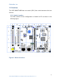
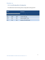
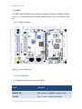
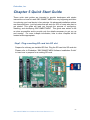
Embedian, Inc. SMART Series Single Board Computer SBC-SMART-MEN 1 SBC-SMART-MEN User’s Manual Document Revision v.1.0 Embedian, Inc. Revision History Revision Date Changes from Previous Revision 1.0 2014/04/08 Initial Release 2 SBC-SMART-MEN User’s Manual Document Revision v.1.0 Embedian, Inc. USER INFORMATION About This Manual This document provides information about products from EMBEDIAN, INC. No warranty of suitability, purpose, or fitness is implied. While every attempt has been made to ensure that the information in this document is accurate, the information contained within is supplied “as-is” and is subject to change without notice. For the circuits, descriptions and tables indicated, EMBEDIAN assumes no responsibility as far as patents or other rights of third parties are concerned. Copyright Notice Copyright © 2013 EMBEDIAN, INC.. All rights reserved. No part of this manual may be reproduced, transmitted, transcribed, stored in a retrieval system, or translated into any language or computer language, in any form or by any means (electronic, mechanical, photocopying, recording, or otherwise), without the express written permission of EMBEDIAN. Trademarks The following lists the trademarks of components used in this board. ARM is a registered trademark of ARM Limited. Android is a registered trademark of Google Linux is a registered trademark of Linus Torvalds. WinCE is a registered trademark of Microsoft TI is a registered trademark of Texas Instruments All other products and trademarks mentioned in this manual are trademarks of their respective owners. Standards EMBEDIAN is ISO 9001:2008 and ISO14001-certified manufacturer. SMARC is an SGET standard for ARM computer on module. Warranty This EMBEDIAN product is warranted against defects in material and workmanship for the warranty period from the date of shipment. During the warranty period, EMBEDIAN will at its discretion, decide to repair or replace defective products. Within the warranty period, the repair of products is free of charge as long as warranty conditions are observed. The warranty does not apply to defects resulting from improper or inadequate maintenance or handling by the buyer, unauthorized modification or misuse, operation outside of the product’s environmental 3 SBC-SMART-MEN User’s Manual Document Revision v.1.0 Embedian, Inc. specifications or improper installation or maintenance. EMBEDIAN will not be responsible for any defects or damages to other products not supplied by EMBEDIAN that are caused by a faulty EMBEDIAN product. Technical Support Technicians and engineers from EMBEDIAN and/or its subsidiaries and official distributors are available for technical support. We are committed to making our product easy to use and will help you use our products in your systems. Before contacting EMBEDIAN technical support, please consult our Web site for the latest product documentation, utilities, and drivers. If the information does not help solve the problem, contact us by e-mail or telephone. 4 SBC-SMART-MEN User’s Manual Document Revision v.1.0 Embedian, Inc. Table of Contents CHAPTER 1 INTRODUCTION................................................................................................................ 9 1.1 FEATURE SET OVERVIEW ............................................................................................................... 9 1.2 BLOCK DIAGRAM .......................................................................................................................... 11 1.3 PERIPHERAL OVERVIEW .............................................................................................................. 13 FIGURE 2: SBC-SMART-MEN PERIPHERAL DIAGRAM ................................................................... 13 1.4 LAYOUT DIAGRAM ......................................................................................................................... 14 FIGURE 3: SBC-SMART-MEN CONNECTORS, HEADERS AND JUMPERS ..................................... 14 1.5 MOUNTING HOLES MECHANICAL DRAWING ........................................................................... 15 1.6 DOCUMENT AND STANDARD REFERENCES.............................................................................. 16 CHAPTER 2 JUMPERS, SWITCHES AND LEDS ................................................................................. 19 2.1 JUMPERS ......................................................................................................................................... 19 FIGURE 5: JUMPER LOCATIONS ....................................................................................................... 19 2.2 SWITCHES ....................................................................................................................................... 23 FIGURE 6: SWITCH LOCATIONS ........................................................................................................ 23 2.3 LEDS ................................................................................................................................................ 25 FIGURE 7: LED LOCATIONS ............................................................................................................... 25 CHAPTER 3 HEADERS AND CONNECTORS ...................................................................................... 27 3.1 CONNECTORS ................................................................................................................................. 27 FIGURE 8: CONNECTOR LOCATIONS (TOP SIDE) .......................................................................... 27 FIGURE 9: CONNECTOR LOCATIONS (BOTTOM SIDE) .................................................................. 28 FIGURE 10: 24-BIT SINGLE PIXEL TRANSMISSION, UNBALANCED ............................................. 36 FIGURE 11: 18-BIT SINGLE PIXEL TRANSMISSION, UNBALANCED.............................................. 39 3.2 HEADERS ........................................................................................................................................ 46 FIGURE 12: HEADER LOCATIONS ..................................................................................................... 46 FIGURE 13: 10-WAY BOX HEADER TO DB9 CABLE ......................................................................... 48 FIGURE 14: PIN ORDER OF P1 AND P2 CONNECTOR.................................................................... 52 CHAPTER 4 I2C0 DEVICES AND CARRIER EEPROM FORMAT ...................................................... 62 4.1 I2C0 DEVICES ................................................................................................................................. 62 4.2 MODULE EEPROM FORMAT ........................................................................................................ 63 4.3 CARRIER EEPROM FORMAT ........................................................................................................ 64 CHAPTER 5 QUICK START GUIDE ..................................................................................................... 67 STEP1. PLUG A WORKING SD CARD INTO SD SLOT ....................................................................... 67 STEP2. CHECK JUMPERS AND SWITCHES ....................................................................................... 68 STEP3. WIRED THE CONSOLE AND ETHERNET CABLE ................................................................. 69 STEP4. POWER 5V TO THE DEVICE................................................................................................... 70 5 SBC-SMART-MEN User’s Manual Document Revision v.1.0 Embedian, Inc. Using this Manual This guide provides information about the Embedian SBC-SMART-MEN Single Board Computer based on TI Sitara AM335x Cortex-A8 processor and SMARC T335X module. Conventions used in this guide This table describes the typographic conventions used in this guide: This Convention Is used for Italic type Emphasis, new terms, variables, and document titles. Filenames, pathnames, and code examples. monospaced type Embedian Information Document Updates Please always check the product specific section on the Embedian support website at www.embedian.com/ for the most current revision of this document. Contact Information For more information about your Embedian products, or for customer service and technical support, contact Embedian directly. To contact Embedian by Use Mail Embedian, Inc. 4F-7. 432 Keelung Rd. Sec. 1, Taipei 11051, Taiwan World Wide Web http://www.embedian.com/ Telephone + 886 2 2722 3291 6 SBC-SMART-MEN User’s Manual Document Revision v.1.0 Embedian, Inc. Additional Resources Please also refer to the most recent SBC-SMART-MEN User’s Manual and TI AM335x processor reference manual and related documentation for additional information. 7 SBC-SMART-MEN User’s Manual Document Revision v.1.0 Embedian, Inc. Introduction This Chapter gives background information on the SBC-SMART-MEN single board computer. Section include: Feature Set Overview Block Diagram Peripheral Overview Layout Diagram Mounting Holes Mechanical Drawing Document and Standard References 8 SBC-SMART-MEN User’s Manual Document Revision v.1.0 Embedian, Inc. Chapter 1 Introduction This document serves as a user manual and technical reference for the EMBEDIAN SBC-SMART-MEN single board computer. The manual is intended for use by engineering personnel working with SBC-SMART-MEN systems. By adding a USB hub and Silicon Lab CP2108 and CP2102, SBC-SMART-MEN expand many RS232s and USB Host ports for users to interface with their legacy devices. SBC-SMART-MEN single board computer is a hybrid approach combines a SMARC COM for the CPU engine with a baseboard for the I/O and application interface. The advantages of this architecture are that system can be easily upgraded by simply changing the SMARC module or expanded by replacing the carrier board. The SMARC module is an industrial standard. 1.1 Feature Set Overview The SBC-SMART-MEN has the following features: Length x Width: 102mm x 145mm (4.0" x 5.7"), 3.5-inch form factor 24-bit color packing, single channel LVDS port. 18-bit color packing, single channel LVDS port 3.3V or 5V LCD signaling option Reset Jumper 5V LED Backlight support 1 x Buzzer 6 x RS232 ports 1 x RS422/RS485 (Share with RS232 Port 1) 3 x USB Host 2.0 1 x USB OTG 1 x Serial-to-USB 2 x Fast Ethernet (10/100Mbps) ports with integrated magnetics. Audio: Microphone Input and Headset Output 1 x CAN Bus (with transceiver) 2 x I2C Bus 11 x GPIOs 2 x SPI Bus Boot Option Switch SD Card slot. 9 SBC-SMART-MEN User’s Manual Document Revision v.1.0 Embedian, Inc. 4-wire Touch Connector RTC backup power sources – Lithium coin cell onboard. 5V input voltage External WDT option Two 4KB EEPROM is provided on I2C0 that holds the board information of SMARC module and Carrier Board. This information includes board name, part number, serial number, and revision information. 10 SBC-SMART-MEN User’s Manual Document Revision v.1.0 Embedian, Inc. 1.2 Block Diagram An overall system block diagram for the SBC-SMART-MEN single board computer is shown on the following page. The following color coding is used on the block diagram: Industry standard wired I/O connectors are shown in orange. Embedian defined wired I/O connectors and headers are shown in red. Industry standard mezzanine and slot format connectors are shown in blue. ICs on the board are shown in pale yellow. Miscellaneous features (jumpers, switches) are shown in drab green. Much may be gleaned from this diagram: What the major features are. An indication of the power supply architecture. 11 SBC-SMART-MEN User’s Manual Document Revision v.1.0 Embedian, Inc. Figure 1: SBC-SMART-MEN Block Diagram Details for this diagram will be explained in the following chapters. 12 SBC-SMART-MEN User’s Manual Document Revision v.1.0 Embedian, Inc. 1.3 Peripheral Overview The following diagram shows the function of all peripherals including of connectors, headers, configuration jumpers and other important features on the SBC-SMART-MEN single board computer. Figure 2: SBC-SMART-MEN Peripheral Diagram 13 SBC-SMART-MEN User’s Manual Document Revision v.1.0 Embedian, Inc. 1.4 Layout Diagram The following section shows the physical location and reference designator of connectors, configuration jumpers and other important features on the SBC-SMART-MEN single board computer. Figure 3: SBC-SMART-MEN Connectors, Headers and Jumpers 14 SBC-SMART-MEN User’s Manual Document Revision v.1.0 Embedian, Inc. 1.5 Mounting Holes Mechanical Drawing Figure 4 shows the mounting holes information of SBC-SMART-MEN. The diameter of mounting hole is 3.2mm and diameter of ring is 6mm. Figure 4: SBC-SMART-MEN Mounting Holes Mechanical Drawing Information 15 SBC-SMART-MEN User’s Manual Document Revision v.1.0 Embedian, Inc. 1.6 Document and Standard References 1.6.1. External Industry Standard Documents eMMC (Embedded Multi-Media Card) the eMMC electrical standard is defined by JEDEC JESD84-B45 and the mechanical standard by JESD84-C44 (www.jedec.org). The I2C Specification, Version 2.1, January 2000, Philips Semiconductor (now NXP) (www.nxp.com). I2S Bus Specification, Feb. 1986 and Revised June 5, 1996, Philips Semiconductor (now NXP) (www.nxp.com). JTAG (Joint Test Action Group defined by IEEE 1149.1-2001 - IEEE Standard Test Access Port and Boundary Scan Architecture (www.ieee.org). MXM3 Graphics Module Mobile PCI Express Module Electromechanical Specification, Version 3.0, Revision 1.1, © 2009 NVIDIA Corporation (www.mxm-sig.org). PICMG® EEEP Embedded EEPROM Specification, Rev. 1.0, August 2010 (www.picmg.org). SD Specifications Part 1 Physical Layer Simplified Specification, Version 3.01, May 18, 2010, © 2010 SD Group and SD Card Association (Secure Digital) (www.sdcard.org). SPI Bus – “Serial Peripheral Interface” - de-facto serial interface standard defined by Motorola. A good description may be found on Wikipedia (http://en.wikipedia.org/wiki/Serial_Peripheral_Interface_Bus). USB Specifications (www.usb.org). 1.6.2. Embedian Documents The following documents are listed for reference. The schematic is not usually available outside of Embedian, without special permission. Contact your Embedian representative for more information. SBC-SMART-MEN User’s Manual SBC-SMART-MEN Pinmux File 1.6.3. TI Documents AM335x ARM Cortex-A8 Microprocessors (MPUs), April 15 2013 (rev. F) 16 SBC-SMART-MEN User’s Manual Document Revision v.1.0 Embedian, Inc. AM335x Schematic Checklist, Oct 31 2011 AM335x ARM Cortex-A8 Microprocessors (MPUs) Technical References Manual, April 15 2013 (rev. H) AM335x Power Consumption Summary, Oct 31 2011 1.6.4. TI Development Tools Pin Mux Utility for ARM® Microprocessors Power Estimation Tool (PET) 1.6.5. TI Software Documents LINUXEZSDK-AM335x ANDROIDDEVKIT-JB-AM335x 1.6.6. Embedian Software Documents SBC-SMART-MEN Linux BSP SBC-SMART-MEN Android BSP SBC-SMART-MEN Linux BSP User’s Guide SBC-SMART-MEN Android BSP User’s Guide 1.6.7. TI Design Network Beaglebone Beaglebone Blask Adeneo Embedded (Windows Embedded Compact 7) Nucleus QNX 17 SBC-SMART-MEN User’s Manual Document Revision v.1.0 Embedian, Inc. Jumpers, Switches and LEDs This Chapter provides SBC-SMART-MEN jumpers, switches and LEDs information. Section include: Jumpers Switches LEDs 18 SBC-SMART-MEN User’s Manual Document Revision v.1.0 Embedian, Inc. Chapter 2 Jumpers, Switches and LEDs This chapter gives detail information of the jumpers, switches and LEDs. 2.1 Jumpers The SBC-SMART-MEN has a number of jumpers that allow you to configure your system to suit your application. All use 2mm shorting blocks (shunts) to select settings. Turn off power to the SBC-SMART-MEN before changing the position of a shunt. 2.1.1. Jumper Location Figure 5: Jumper Locations 19 SBC-SMART-MEN User’s Manual Document Revision v.1.0 Embedian, Inc. 2.1.2. List of Jumpers The table below lists the function of various jumpers. Label Function LVDS_VDD_SEL 3.3V/5V LCD Signaling Voltage UART_RX_SEL RS232/RS422/RS485 Setting for SER0 (UART0) RESET Hardware Reset WDT External WatchDog Timer 2.1.3. Jumper Settings The following tables describe how the jumper shunts to various configurations. LVDS_VDD_SEL: Location on Board, H4 LVDS_VDD_SEL 3.3V/5V LCD Signaling Voltage Setting Function LVDS_VDD_SEL (1-2) 3.3V LVDS_VDD_SEL (2-3) 5V UART_RX_SEL: Location on Board, C2 UART_RX_SEL RS232/RS422/RS485 Settings Setting Function UART_RX_SEL (1-2) RS232 UART_RX_SEL (3-4) RS422/RS485 half duplex UART_RX_SEL (5-6) RS422/RS485 full duplex 20 SBC-SMART-MEN User’s Manual Document Revision v.1.0 Embedian, Inc. RESET: Location on Board, G1 RESET Hardware Reset Setting Function Shunt RESET and Release Hardware Reset Immediately WDT: Location on Board, H1 WDT External Watchdog Timer Setting Function WDT Open Disable External WDT WDT Closed Enable External WDT 2.1.4. Setting Jumpers You configure your board to match the needs of your application by setting jumpers. A jumper is the simplest kind of electric switch. It consists of two metal pins and a small metal clip (often protected by a plastic cover) that slides over the pins to connect them. To “close” a jumper you connect the pins with the clip. To “open” a jumper you remove the clip. Sometimes a jumper will have three pins, labeled 1, 2 and 3. In this case you would connect either pins 1 and 2 or 2 and 3. The jumper settings are schematically depicted in this manual as follows. 21 SBC-SMART-MEN User’s Manual Document Revision v.1.0 Embedian, Inc. A pair of needle-nose pliers may be helpful when working with jumpers. If you have any doubts about the best hardware configuration for your application, contact your sales representative before you make any change. 22 SBC-SMART-MEN User’s Manual Document Revision v.1.0 Embedian, Inc. 2.2 Switches The SBC-SMART-MEN has one switch (SW1) that could determine the boot devices. 2.2.1. Switch Location The SW1 switch for boot configuration is located at D2 as shown in the following figure. Figure 6: Switch Locations 23 SBC-SMART-MEN User’s Manual Document Revision v.1.0 Embedian, Inc. 2.2.2. List of Booting Device Configuration The table below lists the booting device configuration setting by SW1. SW1 Function 1 2 3 Boot Configuration ON OFF OFF Carrier SD Card OFF ON ON Module eMMC Flash ON ON ON Module SPI NOR Flash 24 SBC-SMART-MEN User’s Manual Document Revision v.1.0 Embedian, Inc. 2.3 LEDs The SBC-SMART-MEN has two LEDs to indicate the power to SMARC module and 3.3V of carrier board power status. When power is fine, the LED will light on. 2.3.1. LEDs Location Figure 7: LED Locations 2.3.2. List of LEDs The table below lists the function of LEDs. Label Function SMARC OK ON, if power to SMARC module is fine 3V3 OK ON, if 3.3V of carrier board is fine 25 SBC-SMART-MEN User’s Manual Document Revision v.1.0 Embedian, Inc. Connectors and Headers This Chapter gives SBC-SMART-MEN connectors and headers detail information. Section include: Connectors Headers 26 SBC-SMART-MEN User’s Manual Document Revision v.1.0 Embedian, Inc. Chapter 3 Headers and Connectors This section gives SBC-SMART-MEN connectors and headers detail information. 3.1 Connectors Wired connections to the SBC-SMART-MEN single board computer are described in this section. 3.1.1. Connector Location Top Side Figure 8: Connector Locations (Top Side) 27 SBC-SMART-MEN User’s Manual Document Revision v.1.0 Embedian, Inc. Bottom Side Figure 9: Connector Locations (Bottom Side) 28 SBC-SMART-MEN User’s Manual Document Revision v.1.0 Embedian, Inc. 3.1.2. List of Connectors The table below lists the function of various connectors. Label Function SMARC 314-pin MXM3.0 SMARC Module Connector 5V Power Input 2-pin 4.2mm mini fit male 180D Backlight LCD LED Backlight Connector Touchscreen 4-wire Touch Connector CN3 RTC Backup Battery SD SD/SDHC Connector Buzzer Buzzer LAN1 LAN1 RJ45 Jack with Integrated Magnetic LAN2 LAN2 RJ45 Jack with Integrated Magnetic LVDS1 (Bottom Side) 24-bit Channel LVDS Connector LVDS2 (Bottom Side) 18-bit Channel LVDS Connector CN3 (on Module) JTAG Connector 29 SBC-SMART-MEN User’s Manual Document Revision v.1.0 Embedian, Inc. 3.1.3. Connector Pin Assignments The following tables describe the electrical signals available on the connectors of the SBC-SMART-MEN. Each section provides relevant details about the connector including part numbers, mating connectors, signal descriptions and references to related chapters. Pinout Legend I O I/O P AI AO AIO OD # Input Output Input or output Power Analogue input Analogue output Analogue Input or analogue output Open Drain Signal Low level active signal 30 SBC-SMART-MEN User’s Manual Document Revision v.1.0 Embedian, Inc. 3.1.3.1. Fast LAN RJ45 Connector: LAN1 and LAN2 SBC-SMART-MEN provides with two vertical Fast Ethernet RJ45 connectors (LAN1 and LAN2). The following table shows the pin-out of the LAN1 and LAN2 connectors. LAN1: Location on Board, C4 Header 180D Vertical RJ45 Gigabit Connector Edge Finger Sitara AM335x CPU Pin Signal Name Pin# Ball 1 GBE_MDI0+ Transmit Data+ P30 AO 2 GBE_MDI0‐ Transmit Data‐ P29 AO 3 GBE_MDI1+ Receive Data+ P27 AI 4 GBE_MDI2+ Transmit Data+ P26 5 GBE_MDI2‐ Transmit Data‐ P24 NC 6 GBE_MDI1‐ Receive Data‐ P23 AI 7 GBE_MDI3+ Receive Data+ P20 NC 8 GBE_MDI3‐ Receive Data‐ P19 NC L Left LED Duplex P21/ P22 Yellow R Right LED Link and Ack P25 Green Function Mode From SMSC LAN8720A Type Signal Name NC 31 SBC-SMART-MEN User’s Manual Document Revision v.1.0 Embedian, Inc. LAN2: Location on Board, C5 Header 180D Vertical Gigabit RJ45 Connector Edge Finger Sitara CPU Pin Signal Name Function Pin# Ball 1 GBE1_MDI0+ Transmit Data+ S62 AO 2 GBE1_MDI0‐ Transmit Data‐ S63 AO 3 GBE1_MDI1+ Receive Data+ S65 AI 4 GBE1_MDI2+ Transmit Data+ S66 NC 5 GBE1_MDI2‐ Transmit Data‐ S68 6 GBE1_MDI1‐ Receive Data‐ S69 AI 7 GBE1_MDI3+ Receive Data+ S71 NC 8 GBE1_MDI3‐ Receive Data‐ S72 NC L Left LED Duplex S23/ S24 Yellow R Right LED Link and Ack S55 Green AM335x Mode From SMSC LAN8720A Type Signa l Name NC 32 SBC-SMART-MEN User’s Manual Document Revision v.1.0 Embedian, Inc. 3.1.3.2. SD/SDHC Connector: SD SBC-SMART-MEN provides with one SD/SDHC connector (SD). The SD slot could be used as a boot device or as a standard storage. The following table shows the pin-out of the SD/SDHC connector. SD: Location on Board, H2/H3 Header SD/SDHC Connector Edge Finger Sitara AM335x CPU Pin Signal Name Pin# Ball Mode Signal Name 1 SDIO_CD# SD Insert /SDIO_D3 Detect/ SD receive/trans mit data P35/ P42 U14/ F17 7/0 GPIO1 [18]/ MMC0_ DAT3 I/IO 2 SDIO_CMD SD receive response/ transmit command P34 G18 0 MMC0_ CMD O 3 GND Ground P 4 VDD_SD0 Power P 5 SDIO_CK SD Clock P36 G17 0 MMC0 _CLK I 6 GND Ground 7 SDIO_D0 SD receive/trans mit data P39 G16 0 MMC0_ DAT0 O 8 SDIO_D1 SD receive/trans mit data P40 G15 0 MMC0_ DAT1 O 9 SDIO_D2 SD receive/trans mit data P41 F18 0 MMC0_ DAT2 O 10 SDIO_WP SD Write Protect P33 V14 7 GPIO1 [17] I Function Type P 33 SBC-SMART-MEN User’s Manual Document Revision v.1.0 Embedian, Inc. 3.1.3.3. 24-bit LVDS Connector: LVDS1 SBC-SMART-MEN provides with one 24-bit LCD LVDS connector (LVDS1) and one 18-bit LCD LVDS connector (LVDS2). For flat panel use, parallel LCD data and control information (Red, Green and Blue color data, Display Enable, Vertical Synch and Horizontal Synch) are serialized onto a set of LVDS differential pairs. The information is packed into frames that are 7 bits long. In this section, we will focus on 24-bit LVDS signals. For 24 bit color depths, four LVDS channels are used (24 data bits + 3 control bits + 1 unused bit = 28 bits, or 4 x 7) plus a clock pair. The LVDS clock is transmitted on a separate LVDS pair. The LVDS clock period is 7 times longer than the pixel clock period. The LVDS clock edges are off from the 7 bit frame boundaries by 2 pixel periods. The LVDS signal is implemented from parallel RGB LCD signals via a TI SN75LVDS83B interface IC on carrier board. The following table shows the pin-out of the LVDS1 LCD LVDS connector. LVDS1: Location on Board, I3 (Bottom Side) Header LVDS Connector: *CONN. DF14-20P-1.25H Edge Finger Sitara AM335x CPU Pin Function Pin# Ball Signal Name Mode Type Signal Name 1 1 GND 2 2 GND P 3 3 A3P O 4 4 A3M O 5 5 GND P 6 6 CLKP O 7 7 CLKM O 8 8 GND P 9 9 A2P O 10 10 A2M O 11 11 GND P P 34 SBC-SMART-MEN User’s Manual Document Revision v.1.0 Embedian, Inc. Header LVDS Connector: *CONN. DF14-20P-1.25H Edge Finger Sitara AM335x CPU Pin Function Pin# Ball Signal Name Mode Type Signal Name 12 12 A1P O 13 13 A1M O 14 14 GND P 15 15 A0P O 16 16 A0M O 17 17 GND P 18 18 GND P 19 19 VCC (3.3V or 5V) P 20 20 VCC (3.3V or 5V) P 35 SBC-SMART-MEN User’s Manual Document Revision v.1.0 Embedian, Inc. Note: In the 24-bit single pixel mode, the RGB and control inputs shall be transmitted as shown in the following figure. Outputs A4 through A7 and CLK2 shall be inactive in this mode and fixed at a single value. Bits marked RES are reserved for future use and may take any value. Figure 10: 24-bit Single Pixel Transmission, Unbalanced 36 SBC-SMART-MEN User’s Manual Document Revision v.1.0 Embedian, Inc. 3.1.3.4. 18-bit LVDS Connector: LVDS2 In addition to 24-bit LVDS interface, SBC-SMART-MEN provides with the other 18-bit LCD LVDS connector (LVDS2). It is because that 18-bit LVDS panels and 24-bit LVDS panels are usually not compatible. For 18 bit color depths, the data and control information utilize three LVDS channels (18 data bits + 3 control bits = 21 bits; hence 3 channels with 7 bit frames) plus a clock pair. The LVDS signal is implemented from parallel RGB LCD signals via another TI SN75LVDS83B interface IC on carrier board. The following table shows the pin-out of the LVDS1 LCD LVDS connector. LVDS1: Location on Board, I2 (Bottom Side) Header LVDS Connector: *CONN. DF14-20P-1.25H Edge Finger Sitara AM335x CPU Pin Pin# Ball Signal Name Function Mode Type Signal Name 1 1 GND P 2 2 GND P 3 3 NC NC 4 4 NC NC 5 5 GND P 6 6 CLKP O 7 7 CLKM O 8 8 GND P 9 9 A2P O 10 10 A2M O 11 11 GND P 12 12 A1P O 13 13 A1M O 14 14 GND P 37 SBC-SMART-MEN User’s Manual Document Revision v.1.0 Embedian, Inc. Header LVDS Connector: *CONN. DF14-20P-1.25H Edge Finger Sitara AM335x CPU Pin Pin# Ball Signal Name Function Mode Type Signal Name 15 15 A0P O 16 16 A0M O 17 17 GND P 18 18 GND P 19 19 VCC (3.3V or 5V) P 20 20 VCC (3.3V or 5V) P 38 SBC-SMART-MEN User’s Manual Document Revision v.1.0 Embedian, Inc. Note: In the 18-bit single pixel mode, the RGB and control inputs shall be transmitted as shown in the following figure. Outputs A3 through A7 and CLK2 shall be inactive in this mode and fixed at a single value. Figure 11: 18-bit Single Pixel Transmission, Unbalanced 39 SBC-SMART-MEN User’s Manual Document Revision v.1.0 Embedian, Inc. 3.1.3.5. LCD LED Backlight Connector: Backlight SBC-SMART-MEN provides with one LCD LED backlight connector (Backlight) that can drive up to 10 LEDs in series. The driver IC is TI TPS61165. The following table shows the pin-out of the LED backlight connector. Backlight: Location on Board, A4 LED Backlight Connector: Edge Finger Sitara AM335x CPU Type JST SM02B-BHSS-1-TB or compatible Header Mode Signal Name Pin Signal Name Function Pin# Ball 1 BLH Backlight Drive (Anode Side) From TPS61165 P 2 BLL Backlight Drive (Cathode Side) From TPS61165 P Note: The mating connector is JST BHSR-02VS-1 or compatible. 40 SBC-SMART-MEN User’s Manual Document Revision v.1.0 Embedian, Inc. 3.1.3.6. Power Input 2-pin 4.2mm mini fit male 180D Connector: 5V The power input connector of SBC-SMART-MEN is using a 2-pin 4.2mm locking ramp Molex 39-28-1023 or compatible connectors. The input power shall be 5V. The following table shows the pin-out of the power input connector. 5V: Location on Board, B4 Power Input Connector: Edge Finger Sitara AM335x CPU Pin# Ball Type 2-pin screw type terminal block Header Mode Signal Name Pin Signal Name Function 1 5V 5V Input P 2 GND Ground Power P 3.1.3.7. SMARC Module MXM3 Connector: SMARC The SMARC Module is supported on SMARC connector. This is a 314 pin MXM3 style connector. The SMARC pin-out conforms to the SMARC Module specification. Only 3.3V Module I/O can be supported on the SBC-SMART-MEN single board computer. The MXM3 style connector used on the SBC-SMART-MEN single board computer is with a board-to-board spacing of 5mm. The SBC-SMART-MEN carrier board has captive M2.5 threaded standoffs in the SMARC mounting hole positions. The standoffs accept M2.5 screws, inserted from above, through the Module holes. 3.1.3.8. RTC Backup Battery: CN3 A 6.8mm diameter 3V lithium coin cell battery is available in position CN3. The part number of coin cell battery on CN3 is Seiko MS621F_FL11E. 41 SBC-SMART-MEN User’s Manual Document Revision v.1.0 Embedian, Inc. The battery ‘+’ terminal is protected against charging (as required by safety regulations) by a Schottky diode and a 49.9 Ohm resistor (R10). CN3: Location on Board, H1 3.1.3.9. 4-wire Touch Connector: Touchscreen SBC-SMART-MEN provides with a 4-wire FPC connector for touch panel. The controller is from ADC of the processor. The following table shows the pin-out of the Touchscreen 4-wire resistive connector. Touchscreen: Location on Board, C1 4-wire Touch Connector: Edge Finger Sitara AM335x CPU Type 1.0 ZIF FPC SMT V/T Header Pin Signal Name Function Pin# Ball Mode Signal Name 1 XNUR Left S21 C7 AIN1 AI 2 YPLL Bottom S19 B7 AIN2 AI 3 XPUL Right S18 B6 AIN0 AI 4 YNLR Top S22 A7 AIN3 AI Note: The length of touch FPC cable should not be keeping too long. 42 SBC-SMART-MEN User’s Manual Document Revision v.1.0 Embedian, Inc. 3.1.3.10. Buzzer: Buzzer The buzzer on SBC-SMART-MEN is controlled by PWM (GPIO10). The rated frequency is 2731 + 200Hz. Buzzer: Location on Board, H4 Power Input Connector: Edge Finger Sitara AM335x CPU Ball Type 2-pin screw type terminal block Header Pin Signal Name Function Pin# 1 VDD 3.3V 2 GPIO10 PWM P118 Mode Signal Name P C14 Mode7 GPIO3[7] O 43 SBC-SMART-MEN User’s Manual Document Revision v.1.0 Embedian, Inc. 3.1.3.11. JTAG Connector: CN3 on Module JTAG functions for CPU debug and test are implemented on separate small form factor connector (CN3: JST SM10B-SRSS-TB, 1mm pitch R/A SMD Header) on SMARC module. The JTAG pins are used to allow test equipment and circuit emulators to have access to the Module CPU. The pin-outs shown below are used: The following table shows the pin-out of the CN3 (on module) JTAG connector. CN3: Location on Board, D4 JTAG Connector: Edge Finger Sitara AM335x CPU Type JST SM10B-SRSS-TB, 1mm pitch R/A SMD Header Header Pin Signal Name Function Pin# Ball Mode Signal Name 1 VDD_33A JTAG I/O Voltage (sourced by Module) 2 nTRST JTAG Reset, active low B10 nTRST B10 I 3 TMS JTAG mode select C11 TMS C11 I 4 TDO JTAG data out A11 TDO A11 O 5 TDI JTAG data in B11 TDI B11 I 6 TCK JTAG clock A12 TCK A12 I 7 RTCK JTAG return clock I 8 GND Ground P 9 MFG_Mode# Pulled low to allow in-circuit SPI ROM update I 10 GND P Ground P 44 SBC-SMART-MEN User’s Manual Document Revision v.1.0 Embedian, Inc. Note: The mating connector part number is JST 10SR-3S. 45 SBC-SMART-MEN User’s Manual Document Revision v.1.0 Embedian, Inc. 3.2 Headers This section details the header information of SBC-SMART-MEN single board computer. 3.2.1. Header Location Figure 12: Header Locations 46 SBC-SMART-MEN User’s Manual Document Revision v.1.0 Embedian, Inc. 3.2.2. List of Headers The table below lists the function of various headers. Label Function Console Debug Port P3 SPI1, GPIO11 P1 5 x RS232s, 3 x USB Host 2.0, Serial-to-USB_Client, I2C_GP P2 RS422/485, Audio Mic. In and Headset Out, USB OTG, SPI0, CAN Bus, I2C_LCD, 11 x GPIO 3.2.3. Header Pin Assignments The following tables describe the electrical signals available on the connectors of the SBC-SMART-MEN. Each section provides relevant details about the connector including part numbers, mating connectors, signal descriptions and references to related chapters. Pinout Legend I O I/O P AI AO AIO OD # Input Output Input or output Power Analogue input Analogue output Analogue Input or analogue output Open Drain Signal Low level active signal 47 SBC-SMART-MEN User’s Manual Document Revision v.1.0 Embedian, Inc. 3.2.3.1. Serial Console Debug Connector: Console SBC-SMART-MEN provides with one serial console port that using 2x05 2.0mm box header as the connector. The serial console port is available through a 2.0mm 2x05 header (Console). A 10-way box header to DB9 cable with 20cm long comes with the first-time purchase only and is shown as follows. Figure 13: 10-way box header to DB9 cable Note: The red line on the cable should align to pin 1 of the header. 48 SBC-SMART-MEN User’s Manual Document Revision v.1.0 Embedian, Inc. The following table shows the pin-out of the console serial port header. Console: Location on Board, D2 Header RS232 Header: HEADER DIP 10*2P 180D MALE 2.0mm Edge Finger Sitara AM335x CPU Pin Signal Name Pin# Ball 1 NC 2 NC 3 SER3 _RX 4 NC 5 SER3 _TX 6 Function Mode Type Signal Name P135 K18 1 UART3_RXD I P134 L18 1 UART3_TXD O NC 7 NC 8 NC 9 GND 10 NC Receive Data Transmit Data P 49 SBC-SMART-MEN User’s Manual Document Revision v.1.0 Embedian, Inc. 3.2.3.2. P3 Header: P3 The P3 header of SBC-SMART-MEN reserves SPI1 and GPIO11 function. The following table shows the pin-out of the P3 header. P3: Location on Board, E2 Header CAN Bus Header: HEADER DIP 10*2P 180D MALE 2.0mm Edge Finger Sitara AM335x CPU Pin Signal Name Pin# Ball 1 VDD_ Function Mode Type Signal Name P GPIO P54 C12 3 SPI1_CS0 O CS0# SPI1 Master Chip Select 0 output 3 GPIO11 GPIO P119 B14 7 GPIO3[8] I/O 4 SPI1_ SPI1 Master Chip Select 1 output P55 A15 4 SPI1_CS1 O SPI1 Master Clock output P56 A13 3 SPI1_SCLK O 2 SPI1_ CS1# 5 NC 6 SPI1_ SCLK 50 SBC-SMART-MEN User’s Manual Document Revision v.1.0 Embedian, Inc. Header CAN Bus Header: HEADER DIP 10*2P 180D MALE 2.0mm Edge Finger Sitara AM335x CPU Pin Signal Name Pin# Ball Mode Signal Name 7 NC 8 SPI1_ D12 3 SPI1_D1 MOSI 9 GND 10 SPI1_ MISO Function SPI1 P58 Master Data output (output from CPU, input to SPI device) Type O P SPI1 Master Data input (input to CPU, output from SPI device) P57 B13 3 SPI1_D0 I 51 SBC-SMART-MEN User’s Manual Document Revision v.1.0 Embedian, Inc. 3.2.3.3. P1 Header: P1 The P1 header of SBC-SMART-MEN mainly integrates 5 RS232s, 3 USB Host 2.0 and one serial-to-USB (client) and I2C_GP (can be configured as 2 GPIOs). The connector type is 20*2P Box Header 180D MALE 2.54mm. The following table shows the pin-out of the P1 header. The pin order of P1 and P2 header are as follows. Figure 14: Pin Order of P1 and P2 Connector 52 SBC-SMART-MEN User’s Manual Document Revision v.1.0 Embedian, Inc. P1: Location on Board, A1 P1 Connector (2 x20 2.54mm box header 180 dip) Pin# Pin Name Sitara AM335x CPU Ball Mode Type Description Signal Name SER1 (from CP2108): RS232 1 RXD1 I Receive Data 2 RTS1 O Ready to Send 3 TXD1 O Transmit Data 4 CTS1 I Clear To Send 5 GND1 P Ground SER2 (from CP2108): RS232 6 RXD2 I Receive Data 7 RTS2 O Ready to Send 8 TXD2 O Transmit Data 9 CTS2 I Clear To Send 10 GND2 P Ground 53 SBC-SMART-MEN User’s Manual Document Revision v.1.0 Embedian, Inc. P1 Connector Pin# Pin Name Sitara AM335x CPU Ball Mode Type Description Signal Name SER3 (from CP2108): RS232 11 RXD3 I Receive Data 12 TXD3 O Transmit Data 13 GND3 P Ground SER4 (from CP2108): RS232 14 RXD4 I Receive Data 15 TXD4 O Transmit Data 16 GND4 P Ground SER5 (from CPU UART1): RS232 17 RXD5 I Receive Data 18 TXD5 O Transmit Data 19 GND5 P Ground 54 SBC-SMART-MEN User’s Manual Document Revision v.1.0 Embedian, Inc. P1 Connector Pin# Pin Name Sitara AM335x CPU Ball Mode Type Description Signal Name USB1 Host 2.0 20 USB1_5V * P USB1 -supply (max. 500mA) 21 USB1‐ IO Universal serial bus port 1 (-) 22 USB1+ IO Universal serial bus port 1 (+) 23 USB1_GND P USB Ground USB2 Host 2.0 24 USB2_5V * P USB2 -supply (max. 500mA) 25 USB2‐ IO Universal serial bus port 3 (-) 26 USB2+ IO Universal serial bus port 3 (+) 27 USB2_GND P USB Ground USB3 Host2.0 28 USB3_5V * P USB3 -supply (max. 500mA) 29 USB3‐ IO Universal serial bus port 3 (-) 30 USB3+ IO Universal serial bus port 3 (+) 31 USB3_GND P USB Ground 55 SBC-SMART-MEN User’s Manual Document Revision v.1.0 Embedian, Inc. P1 Connector Pin# Pin Name Sitara AM335x CPU Ball Mode Type Description Signal Name Serial (CPU UART0 and CP2102) to USB Client 32 SERIAL_USB_5V 33 P USB -supply (max. 500mA) SERIAL_USB‐ IO Universal serial bus port (-) 34 SERIAL_USB+ IO Universal serial bus port (+) 35 USB_GND P USB Ground 36 NC Not Connected GPIO (I2C1) 37 GPIO (I2C_GP_CK) D17 Mode7 GPIO0_15 OD LCD display I2C bus clock 38 GPIO (I2C_GP_DAT) D16 Mode7 GPIO0_14 OD General purpose I2C bus data 39 VDD_GPIO P GPIO Power 40 GND_GPIO P GPIO Ground 56 SBC-SMART-MEN User’s Manual Document Revision v.1.0 Embedian, Inc. 3.2.3.4. P2 Header: P2 The P2 header of SBC-SMART-MEN defines RS422/485, USB OTG, Audio Mic. Input and Headset Output, I2C_LCD, CAN Bus, SPI0, and 10 GPIOs. The connector type is also 20*2P Box Header 180D MALE 2.54mm. P2: Location on Board, B1 P2 Connector (2 x20 2.54mm box header 180 dip) Pin# Pin Name Sitara AM335x CPU Ball Mode Type Description Signal Name Audio 1 HP_OUT_R AO Right channel of headset speaker 2 HP_OUT_RR AO HPRCOM Signal of AIC3106 3 AGND AGND Analog Ground 4 HP_OUT_L 5 HP_OUT_LR 6 AUD_33 AI Analogue VDD_IO 7 MIC_R AI Right channel of microphone input 8 MIC_L AI Left channel of microphone input From TLV320AIC3016 Codec Audio Left channel of headset speaker out HPLCOM Signal of AIC3106 57 SBC-SMART-MEN User’s Manual Document Revision v.1.0 Embedian, Inc. P2 Connector Pin# Sitara AM335x CPU Pin Name Ball Type Description Signal Name Mode RS422/485 GND Ground 10 UART1_422_TX+_ 485+ RS422 transmit plus or RS485 plus 11 UART1_422_TX‐_ 485‐ RS422 transmit minus or RS485 minus 12 UART1_422_RX+ RS422 receive plus 13 UART1_422_RX‐ RS422 receive minus 9 P2 Connector Pin# Pin Name Sitara AM335x CPU Ball Mode Type Description P Power Supply Signal Name USB OTG 14 USB0_VBUS 15 USB0‐ N18 0 USB0_DM IO Data‐ 16 USB0+ N17 0 USB0_DP IO Data+ 17 USB0_OTG_ID P16 0 USB0_ID IO Host cable identification 18 GND P Ground 58 SBC-SMART-MEN User’s Manual Document Revision v.1.0 Embedian, Inc. P2 Connector Pin# Sitara AM335x CPU Type Description Pin Name Ball Mode Signal Name SPI0_ A16 0 SPI0_CS0 O SPI0 Master Chip Select 0 output C15 0 SPI0_CS1 O SPI0 Master Chip Select 1 output A17 0 SPIO_SCLK O SPI0 Master Clock output B16 0 SPI0_D1 O SPI0 Master Data output (output from CPU, input to SPI device) B17 0 SPI1_D0 O SPI0 Master Data input (input to CPU, output from SPI device) Type Description P Ground SPI0 19 CS0# 20 SPI0_ CS1# 21 SPI0_ SCLK 22 SPI0_ MOSI 23 SPI0_ MISO P2 Connector Pin# Pin Name Sitara AM335x CPU Ball Mode Signal Name CAN Bus 24 GND 25 CAN0H J18 1 DCAN0_TX O CAN Signal High 26 CAN0L K15 1 DCAN0_RX I CAN Signal Low 59 SBC-SMART-MEN User’s Manual Document Revision v.1.0 Embedian, Inc. P2 Connector Pin# Pin Name Sitara AM335x CPU Ball Mode Signal Name Type Description I2C_LCD 27 I2C_LCD_CK D17 3 I2C2_SCL OD LCD display I2C bus clock 28 I2C_LCD_DAT D18 3 I2C2_SDA OD LCD display I2C bus data Type Description P GPIO Power P Ground P2 Connector Pin# Pin Name Sitara AM335x CPU Ball Mode Signal Name GPIO 29 VDD_ GPIO 30 GND 31 GPIO0 J17 7 GPIO3[4] IO GPIO 32 GPIO1 T6 7 GPIO2[5] IO GPIO 33 GPIO2 U16 7 GPIO1[25] IO GPIO 34 GPIO3 V16 7 GPIO1[24] IO GPIO 35 GPIO4 U6 7 GPIO2[4] IO GPIO 36 GPIO5 T7 7 GPIO2[3] IO GPIO 37 GPIO6 U18 7 GPIO1[28] IO GPIO 38 GPIO7 V6 7 GPIO1[29] IO GPIO 39 GPIO8 T13 7 GPIO2[0] I/O GPIO 40 GPIO9 V12 7 GPIO2[1] I/O GPIO 60 SBC-SMART-MEN User’s Manual Document Revision v.1.0 Embedian, Inc. I2C0 Devices and EEPROM Format This Chapter points out the I2C0 device information and EEPROM format. Section include: I2C Devices on Carrier Module EEPROM Format Carrier EEPROM Format 61 SBC-SMART-MEN User’s Manual Document Revision v.1.0 Embedian, Inc. Chapter 4 I2C0 Devices and Carrier EEPROM Format This chapter introduces I2C0 devices on SBC-SMART-MEN. Also, EEPROM format on carrier board will also be introduced. 4.1 I2C0 Devices There are five I2C devices on the SBC-SMART-MEN and are all on the I2C_PM (I2C0) bus and are operated at 3.3V. Those devices and their address details are listed in the following table: # Device Description Address (8-bit) Address (7-bit) Notes Read Write 0x24 0x49 0x48 General purpose usage address 0x50 0xA1 0xA0 General purpose parameter EEPROM, Serial number, etc in PICMG EEEP format I2C_PM Bus 1 TI TPS65217C 2 On EEPROM Semiconductor CAT64C32 3 Seiko S‐35390A Real-time clock IC 4 TI Audio Codec TLV320AIC3106 0x1B 0x37 0x36 General purpose usage address 5 On EEPROM Semiconductor CAT64C32 0x57 0xAF 0xAE General purpose parameter EEPROM, Serial number, etc in PICMG EEEP format PMIC 0x30 0x61 0x60 General purpose parameter with INT1 register access 62 SBC-SMART-MEN User’s Manual Document Revision v.1.0 Embedian, Inc. 4.2 Module EEPROM Format The SMARC module on SBC-SMART-MEN includes an I2C serial EEPROM available on the I2C_PM bus. An On Semiconductor 24C32 or equivalent EEPROM is used in the module. The device operates at 1.8V. The Module serial EEPROM is placed at I2C slave addresses A2 A1 A0 set to 0 (I2C slave address 50 hex, 7 bit address format or A0 / A1 hex, 8 bit format) (for I2C EEPROMs, address bits A6 A5 A4 A3 are set to binary 0101 convention). The module serial EEPROM is intended to retain module parameter information, including serial number. The module serial EEPROM data structure conforms to the PICMG® EEEP Embedded EEPROM Specification. The EEPROM ID memory layout is now follow the mainline and as follows. Name Size (Bytes) Contents Header 4 MSB 0xEE3355AA LSB Board Name 8 Name for Board in ASCII “SMARCT33” = Embedian SMARC T335X Computer on Module Version 4 Hardware version code for version in ASCII “00A0” = rev. A0 Serial Number 12 Serial number of the board. This is a 12 character string which is: WWYYMS60nnnn Where: WW = 2 digit week of the year of production YY = 2 digit year of production 60 = 600Mhz nnnn = incrementing board number Configuration Option 32 Codes to show the configuration setup on this board. For the available T335X supported, the following codes are used: ASCII = “SMARCT33” = default configuration Remaining 24 bytes are reserved Available 32720 Available space for other non-volatile codes/data 63 SBC-SMART-MEN User’s Manual Document Revision v.1.0 Embedian, Inc. 4.3 Carrier EEPROM Format The SBC-SMART-MEN carrier board includes an I2C serial EEPROM available on the I2C_PM bus. An On Semiconductor 24C32 or equivalent EEPROM is used in the Carrier. The device operates at 3.3V. The Module serial EEPROM is placed at I2C slave addresses A2 A1 A0 set to 1 (I2C slave address 57 hex, 7 bit address format or A0 / A1 hex, 8 bit format) (for I2C EEPROMs, address bits A6 A5 A4 A3 are set to binary 0101 convention). The Carrier serial EEPROM is intended to retain carrier parameter information, including serial number. The carrier serial EEPROM data structure conforms to the PICMG® EEEP Embedded EEPROM Specification. Note: The EEPROM ID memory layout is now follow the mainline and as follows. Name Offset Size Contents (bytes) 0 4 0xAA, 0×55, 0×33, 0xEE EEPROM Format 4 Revision 2 Revision number of the overall format of this EEPROM in ASCII =A0 Header Board Name 6 32 Name of board in ASCII Version 38 4 Hardware version code for board in ASCII Manufacturer 42 16 ASCII name of the manufacturer Part Number 58 16 ASCII Characters for the part number Number of Pins 74 2 Number of pins used by the daughter board 64 SBC-SMART-MEN User’s Manual Document Revision v.1.0 Embedian, Inc. Name Offset Size Contents (bytes) Serial Number 76 12 Serial number of the board. This is a 12 character string which is: WWYYCSMEnnnn Where: WW = 2 digit week of the year of production YY = 2 digit year of production nnnn = incrementing board number Pin Usage 88 148 Two bytes for each configurable 74 pins on the expansion connectors Bit 15: Pin is used or not; 0=Unused by Cape 1=Used by Cape Bit 14-13: Pin Direction; 1 0=Output 01=Input 11=BDIR Bits 12-7: Reserved Bit 6: Slew Rate; 0=Fast 1=Slow Bit 5: Rx Enable; 0=Disabled 1=Enabled Bit 4: Pull Up/Dn Select; 0=Pulldown 1=PullUp Bit 3: Pull Up/DN enabled; 0=Enabled 1=Disabled Bits 2-0: Mux Mode Selection; Mode 0-7 VDD_3V3EXP Current 236 2 Maximum current in milliamps VDD_5V Current 238 2 Maximum current in milliamps SYS_5V Current 240 2 Maximum current in milliamps DC Supplied 242 2 Indicates whether or not the board is supplying voltage on the VDD_5V rail and the current rating 000=No 1-0xFFFF is the current supplied Available 244 32543 Available space for other non-volatile codes/data 65 SBC-SMART-MEN User’s Manual Document Revision v.1.0 Embedian, Inc. Quick Start Guide The purpose of this chapter is to provide a quick start guide so that developers can easily get the board up and running in few minutes. 66 SBC-SMART-MEN User’s Manual Document Revision v.1.0 Embedian, Inc. Chapter 5 Quick Start Guide These quick start guides are intended to provide developers with simple instructions on how to install SBC-SMART-MEN from very beginning and have it monitoring your local device in few minutes. No advanced installation options are discussed here - just the basics that will work for 95% of users who want to get started. This guide will lead you through the process of configuring, installing, and developing SBC-SMART-MEN. This guide was written to be as clear as possible and to provide only the details necessary to get you up and running. For more in-depth information, links to other chapters will be located where appropriate. Step1. Plug a working SD card into SD slot Prepare for a binary pre-installed SD first. Plug the SD card into SD card slot. Please refer to Embedian “SBC-SMART-MEN Software Installation Guide” to learn how to prepare for a working SD card. . 67 SBC-SMART-MEN User’s Manual Document Revision v.1.0 Embedian, Inc. Step2. Check Jumpers and Switches SW1 switch should be set as SD boot (ON OFF OFF) and make sure that RESET jumper is not shunt. . 68 SBC-SMART-MEN User’s Manual Document Revision v.1.0 Embedian, Inc. Step3. Wired the console and Ethernet cable Connect the DB9 to 10-way box header console debug cable from console header of the device to a null modem (TX/RX crossed) cable and connect that null modem cable to your PC. Also connect Ethernet cable from LAN1 of the device to an Ethernet switch. It is illustrated as the following diagram. Open a serial terminal like Putty in your PC. Set the COM port as 115200, 8n1. 69 SBC-SMART-MEN User’s Manual Document Revision v.1.0 Embedian, Inc. Step4. Power 5V to the device Apply 5V to power connector of the device. If you see the LED light on, that means the power is fine. You will see the root filesystem booting. There is no root password required if the root filesystems is Arago. The default root password for Ubuntu root filesystems is “root” (no quotation). Default Ethernet is set as DHCP. 70 SBC-SMART-MEN User’s Manual Document Revision v.1.0