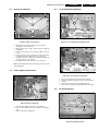
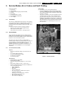
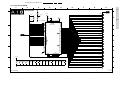
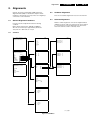
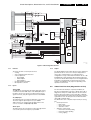
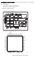
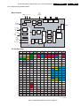
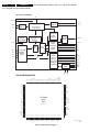
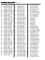
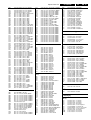
1
Colour Television
Chassis
LC4.2E
AA
E_14490_000.eps
110604
Contents
Page
1. Technical Specifications, Connections,
and Chassis Overview
2
2. Safety and Maintenance Instructions,
Warnings, and Notes
5
3. Directions for Use
7
4. Mechanical Instructions
8
5. Service Modes, Error Codes, and Faultfinding 11
6. Block Diagrams, Testpoint Overviews,
and Waveforms
Wiring Diagram
19
Block Diagram Tuner and IF Video
20
Block Diagram Scaler
21
Testpoint Overview Tv & Scaler Board
22-23
I2C Overview
24
Supply Voltage Overview
25
7. Circuit Diagrams and PWB Layouts
Diagram
Tuner + VIF
(Diagram A1) 26
Hercules
(Diagram A2) 27
Histogram
(Diagram A3) 38
Audio Amplifier
(Diagram A5) 29
TV-Supply
(Diagram A6) 30
Scaler
(Diagram A7) 31
Scaler Interface
(Diagram A9) 32
SDRAM
(Diagram A10) 33
Flash / Control
(Diagram A11) 34
HDMI
(Diagram A12) 35
PCHD-MUX
(Diagram A13) 36
Supply
(Diagram A14) 37
Side IO and LKB Panel
(Diagram D) 48
Rear IO Panel: Scart (17”)
(Diagram H1) 50
Rear IO Panel: PCHD-IO (17”) (Diagram H2) 51
Rear IO Panel: Scart (23/26”)
(Diagram H1) 53
Rear IO Panel: PCHD-IO (23/26”)(Diagram H2) 54
Front IR / LED Panel
(Diagram J) 56
Contents
8.
9.
10
11
Page
Pixel Plus Panel: EPLD Control
Pixel Plus Panel: LVDS In
Pixel Plus Panel: EPLD I/O
Pixel Plus Panel: Power Supply
Alignments
Circuit Descriptions
Abbreviation List
IC Data Sheets
Spare Parts List
Revision List
(Diagram PP1) 57
(Diagram PP2) 58
(Diagram PP3) 59
(Diagram PP4) 60
63
66
72
74
77
82
61
61
61
61
PWB
38-47
38-47
38-47
38-47
38-47
38-47
38-47
38-47
38-47
38-47
38-47
38-47
49
52
52
55
55
56
©
Copyright 2004 Philips Consumer Electronics B.V. Eindhoven, The Netherlands.
All rights reserved. No part of this publication may be reproduced, stored in a
retrieval system or transmitted, in any form or by any means, electronic,
mechanical, photocopying, or otherwise without the prior permission of Philips.
Published by BB 0466 Service PaCE
Printed in the Netherlands
Subject to modification
EN 3122 785 14491
EN 2
1.
Technical Specifications, Connections, and Chassis Overview
LC4.2E AA
1. Technical Specifications, Connections, and Chassis Overview
Note: Figures below can deviate slightly from the actual
situation, due to the different set executions.
1.2
Connections
1.2.1
Rear Connections
AERIAL IN
1.1
Technical Specifications
1.1.1
Vision
Display type
Screen size
Resolution (HxV)
Contrast ratio
Light output
Viewing angle (HxV)
Tuning system
Colour systems
Video playback
Channel selections
Aerial input
Antenna
Dimensions (WxHxD) in mm
1.1.2
Maximum power
1.1.3
:
:
:
:
:
:
:
:
:
:
:
:
:
:
:
:
:
:
:
:
:
:
:
:
:
:
LCD, S-IPS
16:9
17 inch (44 cm)
23 inch (59 cm)
26 inch (66 cm)
1280(*3)x768 pixels
WXGA
400:1
450 cd/m^2
176x176 deg.
PLL
PAL B/G, D/K, I
SECAM B/G, D/K, L,
L1
NTSC 4.43
NTSC 3.58
NTSC Play Back
PAL 60
PAL B/G Play Back
SECAM Play Back
100 presets
UVSH
75 ohm, IEC-type
75 ohm, FM
17 inch: 578x375x240
23 inch: 690x433x240
26 inch: 788x504x270
: FM/FM (5.5-5.74)
: BI NICAM BG - 2CS
BG
: NICAM B/G (5.5-5.85)
: NICAM D/K (6.5-5.85)
(Hung)
: NICAM I (6.0-6.52)
: NICAM L (6.5(AM)5.85)
: 17 inch: 2 x 3 W_rms
: 23 inch: 2 x 5 W_rms
: 26 inch: 2 x 5 W_rms
Miscellaneous
Power supply:
Mains voltage
Mains frequency
: 95 - 240 V_ac
: 50 / 60 Hz
Ambient conditions:
- Temperature range
- Maximum humidity
: +5 to +40 deg. C
: 90 % R.H.
Power consumption
- Normal operation
FM ANT
SCART 1
SCART 2 AUDIO OUT VGA
DVI-D
PC AUDIO IN
E_14490_011.eps
130404
Sound
Sound systems
: <3W
- Standby
Index of this chapter:
1. Technical Specifications
2. Connections
3. Chassis Overview
: 17 inch: 55 W
: 23 inch: 96 W
: 26 inch: 110 W
Figure 1-1 Rear connections
Aerial - In
- IEC-type
Coax, 75 ohm
D
FM Ant
- IEC-type
Coax, 75 ohm
D
External 1: RGB/YUV - In and CVBS - In/Out
20
21
2
1
E_06532_001.eps
050404
Figure 1-2 SCART connector
1
2
3
4
5
6
7
8
9
10
11
12
13
14
15
16
17
18
19
20
21
- Audio - R
0.5 V_rms / 1 kohm
- Audio - R
0.5 V_rms / 10 kohm
- Audio - L
0.5 V_rms / 1 kohm
- Audio - gnd Ground
- Blue - gnd Ground
- Audio - L
0.5 V_rms / 10 kohm
- Blue/U - in 0.7 V_pp / 75 ohm
- CVBS - status 0 - 2 V: INT
4.5 - 7 V: EXT 16:9
9.5 - 12 V: EXT 4:3
- Green - gnd Ground
- n.c.
- Green/Y - in 0.7 V_pp / 75 ohm
- n.c.
- Red - gnd Ground
- FBL - gnd Ground
- Red/V - in 0.7 V_pp / 75 ohm
- Status/FBL 0 - 0.4 V: INT
1 - 3 V: EXT / 75 ohm
- Video
Ground
- Video
Ground
- CVBS - out 1 V_pp / 75 ohm
- CVBS - in 1 V_pp / 75 ohm
- Shielding
Ground
k
j
k
H
H
j
j
H
j
H
H
j
j
H
H
k
j
H
Technical Specifications, Connections, and Chassis Overview
6
7
8
9
10
11
12
13
14
15
16
17
18
19
20
21
22
23
24
C5
External 2: RGB/YUV - In and CVBS - In/Out
20
2
21
1
E_06532_001.eps
050404
Figure 1-3 SCART connector
1
2
3
4
5
6
7
8
9
10
11
12
13
14
15
16
17
18
19
20
21
- Audio - R
0.5 V_rms / 1 kohm
- Audio - R
0.5 V_rms / 10 kohm
- Audio - L
0.5 V_rms / 1 kohm
- Audio - gnd Ground
- Blue - gnd Ground
- Audio - L
0.5 V_rms / 10 kohm
- n.c.
- CVBS - status 0 - 2 V: INT
4.5 - 7 V: EXT 16:9
9.5 - 12 V: EXT 4:3
- Green - gnd Ground
- n.c.
- n.c.
- n.c.
- Red - gnd Ground
- FBL - gnd Ground
- C - in
0.3 V_pp / 75 ohm
- n.c.
- Video
Ground
- Video
Ground
- CVBS - out 1 V_pp / 75 ohm
- CVBS/Y - in 1 V_pp / 75 ohm
- Shielding
Ground
Audio - out
3 - Audio - R
2 - Audio - L
0.5 V_rms / 1 kohm
0.5 V_rms / 1 kohm
k
j
k
H
H
j
j
H
kj
kj
1.2.2
1.
EN 3
k
jk
- SCL_DVI
- SDA_DVI
n.c.
- RX1- RX1+
- Ground
GND
n.c.
n.c.
- +5V
- Ground
GND
- + 5V Hot Plug
- RX0- RX0+
- Ground
GND
n.c.
n.c.
- Ground
GND
- RXC+
- RXC- Ground
GND
PC Audio - in
3 - Audio - R
2 - Audio - L
j
H
H
j
j
H
H
k
j
H
LC4.2E AA
j
j
H
H
j
j
H
H
j
j
H
0.5 V_rms / 1 kohm
0.5 V_rms / 1 kohm
kq
kq
Side connections
HEADPHONE
AUDIO IN
S-VIDEO
E_14490_012.eps
130404
Figure 1-6 Side connections
VGA
1
11
Hosiden: SVHS - In
1 -Y
Ground
2 -C
Ground
3 -Y
1 Vpp / 75 ohm
4 -C
0.3 Vpp / 75 ohm
5
10
6
15
E_06532_002.eps
050404
Figure 1-4 VGA Connector
1
2
3
4
5
6
7
8
9
10
11
12
13
14
15
- Red
- Green
- Blue
- 5V_DC
- DDC_SDA
- H-sync
- V-sync
- DDC_SCL
0.7 V_pp / 75 ohm
0.7 V_pp / 75 ohm
0.7 V_pp / 75 ohm
Ground
Ground
Ground
Ground
Ground
+5 V_dc
Ground
Ground
0-5V
0-5V
j
j
j
H
H
H
H
H
j
H
H
jk
j
j
j
DVI (for 23 and 26 inch models)
1
9
17
8
16
24
C5
E_06532_003.eps
050404
Figure 1-5 DVI connector
1
2
3
4
5
- RX2- RX2+
- Ground
-
GND
n.c.
n.c.
j
j
H
H
H
j
j
Mini Jack: Audio - in
2 - Audio - L
0.5 Vrms / 10 kohm
3 - Audio - R
0.5 Vrms / 10 kohm
jq
jq
Mini Jack: Headphone - Out
- Headphone 32 - 600 ohm / 10 mW
ot
EN 4
1.
LC4.2E AA
Technical Specifications, Connections, and Chassis Overview
LCD PANEL
TV & SCALER
BOARD
PIXEL PLUS PANEL
SIDE IO PANEL
P
POWER SUPPLY
UNIT
A
PP
D
FRONT LED
PANEL
J
REAR I/O
CINCH PANEL
H
E_14490_100.eps
040804
Figure 1-7 Chassis Overview
Safety Instructions, Warnings, and Notes
LC4.2E AA
2.
EN 5
2. Safety Instructions, Warnings, and Notes
2.1
Safety Instructions
Safety regulations require that during a repair:
• Connect the set to the Mains via an isolation transformer (>
800 VA).
• Replace safety components, indicated by the symbol h,
only by components identical to the original ones. Any
other component substitution (other than original type) may
increase risk of fire or electrical shock hazard.
Safety regulations require that after a repair, the set must be
returned in its original condition. Pay in particular attention to
the following points:
• Route the wire trees correctly and fix them with the
mounted cable clamps.
• Check the insulation of the Mains lead for external
damage.
• Check the strain relief of the Mains cord for proper function.
• Check the electrical DC resistance between the Mains plug
and the secondary side (only for sets which have a Mains
isolated power supply):
1. Unplug the Mains cord and connect a wire between the
two pins of the Mains plug.
2. Set the Mains switch to the "on" position (keep the
Mains cord unplugged!).
3. Measure the resistance value between the pins of the
Mains plug and the metal shielding of the tuner or the
aerial connection on the set. The reading should be
between 4.5 Mohm and 12 Mohm.
4. Switch "off" the set, and remove the wire between the
two pins of the Mains plug.
• Check the cabinet for defects, to avoid touching of any
inner parts by the customer.
2.2
•
•
E_06532_006.eps
240604
Figure 2-1 Dolby PL Symbol
2.3.2
•
•
•
All ICs and many other semiconductors are susceptible to
electrostatic discharges (ESD w). Careless handling
during repair can reduce life drastically. Make sure that,
during repair, you are connected with the same potential as
the mass of the set by a wristband with resistance. Keep
components and tools also at this same potential.
Available ESD protection equipment:
– Complete kit ESD3 (small tablemat, wristband,
connection box, extension cable and earth cable) 4822
310 10671.
– Wristband tester 4822 344 13999.
Be careful during measurements in the high voltage
section.
Never replace modules or other components while the unit
is switched "on".
When you align the set, use plastic rather than metal tools.
This will prevent any short circuits and the danger of a
circuit becoming unstable.
2.3
Notes
2.3.1
General
•
•
Measure the voltages and waveforms with regard to the
chassis (= tuner) ground (H), or hot ground (I), depending
on the tested area of circuitry. The voltages and waveforms
shown in the diagrams are indicative. Measure them in the
Service Default Mode (see chapter 5) with a colour bar
signal and stereo sound (L: 3 kHz, R: 1 kHz unless stated
otherwise) and picture carrier at 475.25 MHz for PAL, or
61.25 MHz for NTSC (channel 3).
Where necessary, measure the waveforms and voltages
with (D) and without (E) aerial signal. Measure the
Schematic Notes
•
•
•
•
•
•
Warnings
•
voltages in the power supply section both in normal
operation (G) and in standby (F). These values are
indicated by means of the appropriate symbols.
The semiconductors indicated in the circuit diagram and in
the parts lists, are interchangeable per position with the
semiconductors in the unit, irrespective of the type
indication on these semiconductors.
Manufactured under license from Dolby Laboratories.
“Dolby”, “Pro Logic” and the “double-D symbol”, are
trademarks of Dolby Laboratories.
2.3.3
All resistor values are in ohms and the value multiplier is
often used to indicate the decimal point location (e.g. 2K2
indicates 2.2 kohm).
Resistor values with no multiplier may be indicated with
either an "E" or an "R" (e.g. 220E or 220R indicates 220
ohm).
All capacitor values are given in micro-farads (µ= x10-6),
nano-farads (n= x10-9), or pico-farads (p= x10-12).
Capacitor values may also use the value multiplier as the
decimal point indication (e.g. 2p2 indicates 2.2 pF).
An "asterisk" (*) indicates component usage varies. Refer
to the diversity tables for the correct values.
The correct component values are listed in the Electrical
Replacement Parts List. Therefore, always check this list
when there is any doubt.
Rework on BGA (Ball Grid Array) ICs
General
Although (LF)BGA assembly yields are very high, there may
still be a requirement for component rework. By rework, we
mean the process of removing the component from the PWB
and replacing it with a new component. If an (LF)BGA is
removed from a PWB, the solder balls of the component are
deformed drastically so the removed (LF)BGA has to be
discarded.
Device Removal
As is the case with any component that, it is essential when
removing an (LF)BGA, the board, tracks, solder lands, or
surrounding components are not damaged. To remove an
(LF)BGA, the board must be uniformly heated to a temperature
close to the reflow soldering temperature. A uniform
temperature reduces the chance of warping the PWB.
To do this, we recommend that the board is heated until it is
certain that all the joints are molten. Then carefully pull the
component off the board with a vacuum nozzle. For the
appropriate temperature profiles, see the IC data sheet.
Area Preparation
When the component has been removed, the vacant IC area
must be cleaned before replacing the (LF)BGA.
Removing an IC often leaves varying amounts of solder on the
mounting lands. This excessive solder can be removed with
either a solder sucker or solder wick. The remaining flux can be
removed with a brush and cleaning agent.
After the board is properly cleaned and inspected, apply flux on
the solder lands and on the connection balls of the (LF)BGA.
Note: Do not apply solder paste, as this has shown to result in
problems during re-soldering.
EN 6
2.
LC4.2E AA
Safety Instructions, Warnings, and Notes
Device Replacement
The last step in the repair process is to solder the new
component on the board. Ideally, the (LF)BGA should be
aligned under a microscope or magnifying glass. If this is not
possible, try to align the (LF)BGA with any board markers.
To reflow the solder, apply a temperature profile according to
the IC data sheet. So as not to damage neighbouring
components, it may be necessary to reduce some
temperatures and times.
More Information
For more information on how to handle BGA devices, visit this
URL: http://www.atyourservice.ce.philips.com (needs
subscription). After login, select “Magazine”, then go to
“Workshop Information”. Here you will find Information on how
to deal with BGA-ICs.
2.3.4
Lead Free Solder
Some PWBs in this chassis are “lead-free prepared”. This is
indicated on the PWB by the PHILIPS lead-free logo (either by
a service-printing or by a sticker). It does not mean that leadfree solder is actually used!
P
b
Figure 2-2 Lead-free logo
2.3.5
Practical Service Precautions
•
•
It makes sense to avoid exposure to electrical shock.
While some sources are expected to have a possible
dangerous impact, others of quite high potential are of
limited current and are sometimes held in less regard.
Always respect voltages. While some may not be
dangerous in themselves, they can cause unexpected
reactions - reactions that are best avoided. Before reaching
into a powered TV set, it is best to test the high voltage
insulation. It is easy to do, and is a good service precaution.
Directions for Use
3. Directions for Use
You can download this information from the following website:
http://www.philips.com/support
LC4.2E AA
3.
EN 7
EN 8
4.
Mechanical Instructions
LC4.2E AA
4. Mechanical Instructions
Index of this chapter:
1. Service Position
2. Rear Cover Removal
3. Power Supply Unit Removal
4. TV & Scaler Board Removal
5. I/O Panel Removal
6. Side I/O & Keyboard Panel and Front LED Panel Removal
7. Pixel Plus Panel Removal
8. Exchanging the LCD Panel
9. Re-assembly
4
Note: Figures below can deviate from the actual situation, due
to different set executions.
Note: To diagnose the set with ComPair it is not needed to
open the set entirely.
1. Manually unlock and remove the cover cap (1). See figure
“TV set rear view”.
2. Break away the protective plate (2) at the I/O panel bracket
to get access to the needed plugs. See figure “Protective
plate”.
E_14490_003.eps
130404
Figure 4-3 TV stand removal
1. Carefully pull upwards the cover plate (2) (from it’s left side)
to unlock it (3) and remove the plate from the stand.
2. Unplug the AC power and the antenna cables.
3. Be sure to remove the coin slotted mounting screw (4) from
the stand.
4. Carefully lift the TV from the swivel base (it uses a vertical
sliding mechanism).
5. Place the TV upside down on a tabletop (use a protection
sheet or foam bars). Take care, that this is flat and free
from obstacles like screws, to prevent damaging the fragile
LCD screen.
2
E_14490_001.eps
130404
4.1.1
Foam Bars
Figure 4-1 Protective plate
4.1
Service Position
5
1
E_06532_018.eps
170504
Figure 4-4 Foam bars
2
3
E_14490_002.eps
130404
Figure 4-2 TV set rear view
The foam bars (order code 3122 785 90580) can be used for
all types and sizes of Flat TVs. By laying the plasma or LCD TV
flat on the (ESD protective) foam bars, a stable situation is
created to perform measurements and alignments. By placing
a mirror under the TV, you can easily monitor the screen.
Mechanical Instructions
4.2
4.4
Rear Cover Removal
3
LC4.2E AA
4.
EN 9
TV & Scaler Board Removal
3
3
3
1
1
3
2
2
3
1
3
3
E_14490_006.eps
130404
E_14490_004.eps
130404
Figure 4-7 : TV & Scaler board shield removal
Figure 4-5 Rear cover removal
1. Manually unlock and remove the top cover cap (5).
See Figure: “TV set rear view”.
2. Make sure all power-, audio-, video- and coax- cables are
unplugged.
3. Remove all Torx screws (1) around the edges of the rear
cover.
4. Remove the four silver coloured Torx screws (2) around
the stand holder. See figure “Rear cover removal”.
5. Carefully use a flat screwdriver to release the clamps (3).
See figure “Rear cover removal”.
6. Remove the rear cover and store it in a safe place.
2
3
Note: avoid holding the button-area during removal (it can be
easily damaged).
4.3
Power Supply Unit Removal
E_14490_007.eps
130404
Figure 4-8 : TV & Scaler board removal
1. Disconnect all cables from the TV & Scaler board.
2. Remove all shield mounting screws (1) and remove the
shield.
3. Remove the screw from the grounding cable (2).
4. Remove the mounting screw (3) and remove the board.
1
4.5
I/O Panel Removal
3
E_14520_005.eps
100204
1
Figure 4-6 Power supply unit
1. Disconnect all cables from the Power supply unit.
2. Remove all mounting screws (1) from the Power supply
unit.
3. Take out the Power supply unit.
2
E_14490_008.eps
130404
Figure 4-9 I/O panel removal
EN 10
4.
LC4.2E AA
Mechanical Instructions
1. Release the two clamps (1) at the I/O panel bracket.
Carefully pull the bracket in the direction (2), as shown at
the figure “I/O panel removal”, and remove it.
2. Disconnect all cables from the I/O panel.
3. Remove all mounting screws from the I/O panel (3).
4. Take out the I/O panel.
4.6
4.8
Exchanging the LCD Panel
Side I/O & Keyboard Panel and Front LED
Panel Removal
1
1
1
4
2
3
E_14490_010.eps
130404
1
Figure 4-12 Exchanging the LCD panel
1.
2.
3.
4.
E_14490_009.eps
130404
Figure 4-10 Side I/O & Keyboard panel and
Front LED panel removal
1. Release the clamp (1) and take out the Front LED panel.
2. Disconnect the cable (2) from the Side I/O & Keyboard
panel.
3. Remove all mounting screws (3) from the Side I/O &
Keyboard panel bracket.
4. Unlock this unit by shifting it to the outside direction of the
monitor.
5. Release the clamp (4) and take out the Side I/O &
Keyboard panel from the bracket.
4.7
4.9
Disconnect all cables from the LCD Panel.
Remove all mounting screws (1) from the metal cover.
Lift and take off the metal cover.
Now you can exchange the LCD panel.
Re-Assembly
To re-assemble the whole set, do all processes in reverse
order.
Notes:
• Do not forget to replace the ground cable of the TV &
Scaler board, while mounting the screw at the board
topside. See figure “TV & Scaler board removal”.
• Make sure the ferrite ring (1) is properly tightened to the clip
(this is valid only for 26 inch sets).
1
Pixel Plus Panel Removal
1
E_14490_055.eps
070504
Figure 4-13 Ferrite ring
E_14520_005.eps
100204
Figure 4-11 Pixel Plus panel removal
1. Disconnect all cables from the Pixel Plus panel.
2. Remove all mounting screws from the Pixel Plus panel.
3. Take out the Pixel Plus panel.
Service Modes, Error Codes, and Fault Finding
LC4.2E AA
5.
EN 11
5. Service Modes, Error Codes, and Fault Finding
Index of this chapter:
1. Test Points
2. Service Modes
3. Problems and Solving Tips (related to CSM)
4. ComPair
5. Error Codes
6. The Blinking LED Procedure
7. Fault Finding and Repair Tips
8. Power Supply
5.1
Test Points
This chassis is equipped with test points in the service printing.
In the schematics test points are identified with a rectangle box
around Fxxx or Ixxx. These test points are specifically
mentioned in the service manual as “half moons” with a dot in
the centre.
Perform measurements under the following conditions:
• Television set in Service Default Alignment Mode.
• Video input: Colour bar signal.
• Audio input: 3 kHz left channel, 1 kHz right channel.
5.2
How to enter
To enter SDM, use one of the following methods:
• Press the following key sequence on the remote control
transmitter: “062596” directly followed by the MENU button
(do not allow the display to time out between entries while
keying the sequence).
• Short "Service" jumpers on the TV board during cold start
and apply mains (see Figure "Service jumpers"). Then
press the mains button (remove the short after start-up).
Caution: Entering SDM by shorting "Service" jumpers will
override the +8V-protection. Do this only for a short period.
When doing this, the service-technician must know exactly
what he is doing, as it could damage the television set.
• Or via ComPair.
1
Service Modes
Service Default mode (SDM) and Service Alignment Mode
(SAM) offers several features for the service technician, while
the Customer Service Mode (CSM) is used for communication
between the call centre and the customer.
This chassis also offers the option of using ComPair, a
hardware interface between a computer and the TV chassis. It
offers the abilities of structured troubleshooting, error code
reading, and software version readout for all chassis.
Minimum requirements for ComPair: a Pentium processor, a
Windows OS, and a CD-ROM drive (see also paragraph
"ComPair").
5.2.1
Service Default Mode (SDM)
Purpose
• To create a predefined setting for measurements to be
made.
• To override software protections.
• To start the blinking LED procedure.
• To inspect the error buffer.
• To check the life timer.
Specifications
• Tuning frequency: 475.25 MHz.
• Colour system: PAL-BG.
• All picture settings at 50% (brightness, colour contrast,
hue).
• Bass, treble and balance at 50 %; volume at 25 %.
• All service-unfriendly modes (if present) are disabled. The
service unfriendly modes are:
– Timer / Sleep timer.
– Child / parental lock.
– Blue mute.
– Hotel / hospital mode.
– Auto shut off (when no “IDENT” video signal is
received for 15 minutes).
– Skipping of non-favourite presets / channels.
– Auto-storage of personal presets.
– Auto user menu time-out.
– Auto Volume Levelling (AVL).
E_14490_056.eps
070504
Figure 5-1 E Service jumpers
EN 12
5.
Service Modes, Error Codes, and Fault Finding
LC4.2E AA
After entering SDM, the following screen is visible, with SDM in
the upper right corner of the screen to indicate that the
television is in Service Default Alignment Mode.
00022
LC42EP1 0.08/S42GV1 0.90
SDM
ERR 0 0 0 0 0
After entering SAM, the following screen is visible, with SAM in
the upper right corner of the screen to indicate that the
television is in Service Alignment Mode.
00022 LC42EP1 0.08/S42GV1 0.90
ERR 0 0 0 0 0
SAM
OP 000 057 140 032 120 128 000
OP 000 057 140 032 120 128 000
. Clear
. Options
. Tuner
. White Tone
. Audio
. NVM Editor
. SC NVM Editor
Clear ?
. ComPair Mode
On
E_14490_051.eps
220404
Figure 5-2 SDM menu
How to navigate
Use one of the following methods:
• When you press the MENU button on the remote control,
the set will switch on the normal user menu in the SDM
mode.
• On the TV, press and hold the VOLUME DOWN and press
the CHANNEL DOWN for a few seconds, to switch from
SDM to SAM and reverse.
How to exit
Switch the set to STANDBY by pressing the mains button on
the remote control transmitter or the television set.
If you turn the television set off by removing the mains (i.e.,
unplugging the television) without using the mains button, the
television set will remain in SDM when mains is re-applied, and
the error buffer is not cleared.
5.2.2
Service Alignment Mode (SAM)
Purpose
• To change option settings.
• To display / clear the error code buffer.
• To perform alignments.
Specifications
• Operation hours counter (maximum five digits displayed).
• Software version, Error codes, and Option settings display.
• Error buffer clearing.
• Option settings.
• AKB switching.
• Software alignments (Tuner, White Tone, Geometry &
Audio).
• NVM Editor.
• ComPair Mode switching.
How to enter
To enter SAM, use one of the following methods:
• Press the following key sequence on the remote control
transmitter: “062596" directly followed by the OSD/
STATUS button (do not allow the display to time out
between entries while keying the sequence).
• Or via ComPair.
E_14490_052eps
220404
Figure 5-3 SAM menu
Menu explanation
1. LLLLL. This represents the run timer. The run timer counts
normal operation hours, but does not count standby hours.
2. AAAABCD-X.Y/ EEEEEE F.GG. This is the software
identification of the main microprocessor followed by the
software identification for the scaler IC:
– A= the project name (LC42).
– B= the region: E= Europe, A= Asia Pacific, U= NAFTA,
L= LATAM.
– C= the software diversity:
• Europe: T= 1 page TXT, F= Full TXT, V= Voice
control.
• LATAM and NAFTA: N= Stereo non-dBx, S=
Stereo dBx.
• Asian Pacific: T= TXT, N= non-TXT, C= NTSC.
• ALL regions: M= mono, D= DVD, Q= Mk2.
– D= the language cluster number.
– X= the main software version number (updated with a
major change that is incompatible with previous
versions).
– Y= the sub software version number (updated with a
minor change that is compatible with previous
versions).
– EEEEEE= the scaler sw cluster
– F= the main sw version no.
– GG= the sub-version no.
3. SAM. Indication of the Service Alignment Mode.
4. Error Buffer. Shows all errors detected since the last time
the buffer was erased. Five errors possible.
5. Option Bytes. Used to set the option bytes. See “Options”
in the Alignments section for a detailed description. Seven
codes are possible.
6. Clear. Erases the contents of the error buffer. Select the
CLEAR menu item and press the MENU RIGHT key. The
content of the error buffer is cleared.
7. Options. Used to set the option bits. See “Options” in the
Alignments section for a detailed description.
8. Tuner. Used to align the tuner. See “Tuner” in the
Alignments section for a detailed description.
9. White Tone. Used to align the white tone. See “White
Tone” in the Alignments section for a detailed description.
10. Audio. No audio alignment is necessary for this television
set.
Service Modes, Error Codes, and Fault Finding
11. NVM Editor. Can be used to change the NVM data in the
television set. See table “NVM data” further on.
12. SC NVM Editor. Can be used to edit Scaler NVM.
13. ComPaIr. Can be used to switch on the television to In
System Programming (ISP) mode, for software uploading
via ComPair.
Caution: When this mode is selected without ComPair
connected, the TV will be blocked. Remove the AC power
to reset the TV.
1 00022
LC42EP1 0.08/S42GV1 0.90 CSM
5
6 NOT TUNED
7 PAL
8 STEREO
9 CO 50 CL 50 BR 50
0 AVL Off
E_14490_053.eps
230404
Figure 5-4 CSM menu
Menu explanation
1. Indication of the decimal value of the operation hours
counter, Software identification of the main microprocessor
(see "Service Default or Alignment Mode" for an
explanation), and the service mode (CSM= Customer
Service Mode).
2. Displays the last five errors detected in the error code
buffer.
3. Displays the option bytes.
4. Displays the type number version of the set.
5. Reserved item for P3C call centres (AKBS stands for
Advanced Knowledge Base System).
6. Indicates the television is receiving an "IDENT" signal on
the selected source. If no "IDENT" signal is detected, the
display will read "NOT TUNED"
7. Displays the detected Colour system (e.g. PAL/NTSC).
8. Displays the detected Audio (e.g. stereo/mono).
9. Displays the picture setting information.
10. Displays the sound setting information.
How to exit
Switch the set to STANDBY by pressing the mains button on
the remote control transmitter or the television set.
If you turn the television set “off” by removing the mains (i.e.,
unplugging the television) without using the mains button, the
television set will remain in SAM when mains is re-applied, and
the error buffer is not cleared.
Customer Service Mode (CSM)
Purpose
The Customer Service Mode shows error codes and
information on the TV’s operation settings. The call centre can
instruct the customer (by telephone) to enter CSM in order to
identify the status of the set. This helps the call centre to
diagnose problems and failures in the TV set before making a
service call.
The CSM is a read-only mode; therefore, modifications are not
possible in this mode.
Upon entering the Customer Service Mode, the following
screen will appear:
EN 13
4
How to store SAM settings
To store the settings changed in SAM mode, leave the top level
SAM menu by using the POWER button on the remote control
transmitter or the television set.
How to enter
To enter CSM, press the following key sequence on the remote
control transmitter: “123654” (do not allow the display to time
out between entries while keying the sequence).
5.
2 CODES 0 0 0 0 0
3 OP 000 057 140 032 120 128 000
How to navigate
• In SAM, select menu items with the MENU UP/DOWN keys
on the remote control transmitter. The selected item will be
highlighted. When not all menu items fit on the screen, use
the MENU UP/DOWN keys to display the next / previous
menu items.
• With the MENU LEFT/RIGHT keys, it is possible to:
– Activate the selected menu item.
– Change the value of the selected menu item.
– Activate the selected submenu.
• In SAM, when you press the MENU button twice, the set
will switch to the normal user menus (with the SAM mode
still active in the background). To return to the SAM menu
press the MENU or STATUS/EXIT button.
• When you press the MENU key in while in a submenu, you
will return to the previous menu.
5.2.3
LC4.2E AA
How to exit
To exit CSM, use one of the following methods:
• Press the MENU, STATUS/EXIT, or POWER button on the
remote control transmitter.
• Press the POWER button on the television set.
5.3
Problems and Solving Tips Related to CSM
5.3.1
Picture Problems
Note: The problems described below are all related to the TV
settings. The procedures used to change the value (or status)
of the different settings are described.
Picture too dark or too bright
If:
• The picture improves when you press the AUTO PICTURE
button on the remote control transmitter, or
• The picture improves when you enter the Customer
Service Mode,
EN 14
5.
LC4.2E AA
Service Modes, Error Codes, and Fault Finding
6. Press the MENU RIGHT key to increase the COLOUR
value.
7. Press the MENU button on the remote control transmitter
twice to exit the user menu.
8. The new PERSONAL preference value is automatically
stored.
Then:
1. Press the AUTO PICTURE button on the remote control
transmitter repeatedly (if necessary) to choose
PERSONAL picture mode.
2. Press the MENU button on the remote control transmitter.
This brings up the normal user menu.
3. In the normal user menu, use the MENU UP/DOWN keys
to highlight the PICTURE sub menu.
4. Press the MENU LEFT/RIGHT keys to enter the PICTURE
sub menu.
5. Use the MENU UP/DOWN keys (if necessary) to select
BRIGHTNESS.
6. Press the MENU LEFT/RIGHT keys to increase or
decrease the BRIGHTNESS value.
7. Use the MENU UP/DOWN keys to select PICTURE.
8. Press the MENU LEFT/RIGHT keys to increase or
decrease the PICTURE value.
9. Press the MENU button on the remote control transmitter
twice to exit the user menu.
10. The new PERSONAL preference values are automatically
stored.
Menu text not sharp enough
If:
• The picture improves after you have pressed the AUTO
PICTURE button on the remote control transmitter,
Then:
1. Press the AUTO PICTURE button on the remote control
transmitter repeatedly (if necessary) to choose
PERSONAL picture mode.
2. Press the MENU button on the remote control transmitter.
This brings up the normal user menu.
3. In the normal user menu, use the MENU UP/DOWN keys
to highlight the PICTURE sub menu.
4. Press the MENU LEFT/RIGHT keys to enter the PICTURE
sub menu.
5. Use the MENU UP/DOWN keys to select PICTURE.
6. Press the MENU LEFT key to decrease the PICTURE
value.
7. Press the MENU button on the remote control transmitter
twice to exit the user menu.
8. The new PERSONAL preference value is automatically
stored.
White line around picture elements and text
If:
The picture improves after you have pressed the AUTO
PICTURE button on the remote control transmitter,
Then:
1. Press the AUTO PICTURE button on the remote control
transmitter repeatedly (if necessary) to choose
PERSONAL picture mode.
2. Press the MENU button on the remote control transmitter.
This brings up the normal user menu.
3. In the normal user menu, use the MENU UP/DOWN keys
to highlight the PICTURE sub menu.
4. Press the MENU LEFT/RIGHT keys to enter the PICTURE
sub menu.
5. Use the MENU UP/DOWN keys to select SHARPNESS.
6. Press the MENU LEFT key to decrease the SHARPNESS
value.
7. Press the MENU button on the remote control transmitter
twice to exit the user menu.
8. The new PERSONAL preference value is automatically
stored.
5.4
ComPair
5.4.1
Introduction
ComPair (Computer Aided Repair) is a service tool for Philips
Consumer Electronics products. ComPair is a further
development on the European DST (service remote control),
which allows faster and more accurate diagnostics. ComPair
has three big advantages:
ComPair helps you to quickly get an understanding on how to
repair the chassis in a short time by guiding you systematically
through the repair procedures.
ComPair allows very detailed diagnostics (on I2C level) and is
therefore capable of accurately indicating problem areas. You
do not have to know anything about I2C commands yourself
because ComPair takes care of this.
ComPair speeds up the repair time since it can automatically
communicate with the chassis (when the microprocessor is
working) and all repair information is directly available. When
ComPair is installed together with the SearchMan electronic
manual of the defective chassis, schematics and PWBs are
only a mouse click away.
Snowy picture
Check CSM line 6. If this line reads “Not Tuned”, check the
following:
• Antenna not connected. Connect the antenna.
• No antenna signal or bad antenna signal. Connect a proper
antenna signal.
• The tuner is faulty (in this case line 2, the Error Buffer line,
will contain error number 10). Check the tuner and replace/
repair the tuner if necessary.
5.4.2
Specifications
Black and white picture
If:
• The picture improves after you have pressed the AUTO
PICTURE button on the remote control transmitter,
Then:
1. Press the AUTO PICTURE button on the remote control
transmitter repeatedly (if necessary) to choose
PERSONAL picture mode.
2. Press the MENU button on the remote control transmitter.
This brings up the normal user menu.
3. In the normal user menu, use the MENU UP/DOWN keys
to highlight the PICTURE sub menu.
4. Press the MENU LEFT/RIGHT keys to enter the PICTURE
sub menu.
5. Use the MENU UP/DOWN keys to select COLOUR.
ComPair consists of a Windows based faultfinding program
and an interface box between PC and the (defective) product.
The ComPair interface box is connected to the PC via a serial
or RS232 cable.
In this chassis, the ComPair interface box and the TV
communicate via a bi-directional service cable via the service
connector.
The ComPair faultfinding program is able to determine the
problem of the defective television. ComPair can gather
diagnostic information in two ways:
• Automatic (by communication with the television):
ComPair can automatically read out the contents of the
entire error buffer. Diagnosis is done on I2C level. ComPair
can access the I2C bus of the television. ComPair can
send and receive I2C commands to the micro controller of
the television. In this way, it is possible for ComPair to
Service Modes, Error Codes, and Fault Finding
communicate (read and write) to devices on the I2C
busses of the TV-set.
• Manually (by asking questions to you): Automatic
diagnosis is only possible if the micro controller of the
television is working correctly and only to a certain extend.
When this is not the case, ComPair will guide you through
the faultfinding tree by asking you questions (e.g. Does the
screen give a picture? Click on the correct answer: YES /
NO) and showing you examples (e.g. Measure test-point I7
and click on the correct waveform you see on the
oscilloscope). You can answer by clicking on a link (e.g.
text or a waveform picture) that will bring you to the next
step in the faultfinding process.
By a combination of automatic diagnostics and an interactive
question / answer procedure, ComPair will enable you to find
most problems in a fast and effective way.
Beside fault finding, ComPair provides some additional
features like:
• Up- or downloading of pre-sets.
• Managing of pre-set lists.
• If both ComPair and SearchMan (Electronic Service
Manual) are installed, all the schematics and the PWBs of
the set are available by clicking on the appropriate
hyperlink. Example: Measure the DC-voltage on capacitor
C2568 (Schematic/Panel) at the Mono-carrier.
– Click on the 'Panel' hyperlink to automatically show the
PWB with a highlighted capacitor C2568.
– Click on the 'Schematic' hyperlink to automatically
show the position of the highlighted capacitor.
5.4.3
5.4.4
LC4.2E AA
5.
EN 15
How To Order
ComPair order codes (EU/AP/LATAM):
• Starter kit ComPair32/SearchMan32 software and
ComPair interface (excl. transformer): 3122 785 90450.
• ComPair interface (excluding transformer):
4822 727 21631.
• Starter kit ComPair32 software (registration version): 3122
785 60040.
• Starter kit SearchMan32 software: 3122 785 60050.
• ComPair32 CD (update): 3122 785 60070 (year 2002,
3122 785 60110 (year 2003).
• SearchMan32 CD (update): 3122 785 60080 (year 2002),
3122 785 60120 (year 2003), 3122 785 60130 (year 2004).
• ComPair interface cable: 3122 785 90004.
• ComPair firmware upgrade IC: 3122 785 90510.
• Transformer (non-UK): 4822 727 21632.
• Transformer UK: 4822 727 21633.
• Additional ComPair interface cable: 3139 131 0379.
Note: If you encounter any problems, contact your local
support desk.
5.5
Error Codes
The error code buffer contains all errors detected since the last
time the buffer was erased. The buffer is written from left to
right. When an error occurs that is not yet in the error code
buffer, it is displayed at the left side and all other errors shift one
position to the right.
How To Connect
5.5.1
1. First, install the ComPair Browser software (see the Quick
Reference Card for installation instructions).
2. Connect the RS232 interface cable between a free serial
(COM) port of your PC and the PC connector (marked with
'PC') of the ComPair interface.
3. Connect the mains adapter to the supply connector
(marked with 'POWER 9V DC') of the ComPair interface.
4. Switch the ComPair interface “off”.
5. Switch the television set “off” with the mains switch.
6. Connect the ComPair interface cable with the connector on
the rear side of the ComPair interface (marked with 'I2C')
and the additional ComPair interface cable. Connect the
other side of the additional ComPair interface cable with
the ComPair (or Service) connector at the rear side of the
TV.
7. Plug the mains adapter in a mains outlet, and switch the
interface “on”. The green and red LEDs light up together.
The red LED extinguishes after approx. 1 second while the
green LED remains lit.
8. Start the ComPair program and read the 'Introduction'
chapter.
You can read the error buffer in 3 ways:
• On screen via the SAM (if you have a picture).
Examples:
– ERROR: 0 0 0 0 0 : No errors detected
– ERROR: 6 0 0 0 0 : Error code 6 is the last and only
detected error
– ERROR: 9 6 0 0 0 : Error code 6 was detected first and
error code 9 is the last detected (newest) error
• Via the blinking LED procedure (when you have no
picture). See “The Blinking LED Procedure”.
• Via ComPair.
5.5.2
VCR
Power
9V DC
Figure 5-5 ComPair Interface connection
Note: If you exit SAM by disconnecting the mains from the
television set, the error buffer is not reset.
I2C
E_06532_008.eps
190204
How To Clear The Error Buffer
The error code buffer is cleared in the following cases:
• By using the CLEAR command in the SAM menu:
– To enter SAM, press the following key sequence on the
remote control transmitter: “062596” directly followed
by the OSD/STATUS button (do not allow the display
to time out between entries while keying the
sequence).
– Make sure the menu item CLEAR is highlighted. Use
the MENU UP/DOWN buttons, if necessary.
– Press the MENU RIGHT button to clear the error
buffer. The text on the right side of the “CLEAR” line will
change from “CLEAR?” to “CLEARED”
• If the contents of the error buffer have not changed for 50
hours, the error buffer resets automatically.
TO SERVICE
CONNECTOR
PC
How To Read The Error Buffer
5.5.3
Error Codes
In case of non-intermittent faults, write down the errors present
in the error buffer and clear the error buffer before you begin
the repair. This ensures that old error codes are no longer
present.
EN 16
5.
Service Modes, Error Codes, and Fault Finding
LC4.2E AA
If possible, check the entire contents of the error buffer. In
some situations, an error code is only the result of another error
and not the actual cause of the problem (for example, a fault in
the protection detection circuitry can also lead to a protection).
5.7.2
In case a blank NVM is placed or when the NVM content is
corrupted, default values can be downloaded into the NVM.
After the default values are downloaded it will be possible to
start up and to start aligning the TV set. This is no longer
initiated automatically; to initiate the download the following
action has to be performed:
1. Switch off the TV set via the mains switch
2. Short circuit the SDM jumpers (keep short circuited)
3. Press P+ or Ch+ on the local keyboard (and keep it
pressed)
4. Switch on the TV set via the mains switch
5. When the set has started up the P+/Ch+ button can be
released and the short circuit of the SDM jumpers can be
removed.
6. The red LED will be on continuously to indicate that the
download is initiated (normally when SDM is activated the
red LED will start with the Blinking LED sequence).
7. Wait +/- 30 Seconds (time needed to download default
values to the NVM)
Result: The set is in SDM, the NVM is loaded with default
values and the blinking LED is not activated (The blinking LED
is not activated in this case to show that the download has been
performed), the LED will be on.
Table 5-1 Error code overview
5.6
Error
Device
Error description
0
Not applicable
No Error
1
Not applicable
-
-
-
2
Not applicable
-
-
-
3
Not applicable
-
-
-
4
GM1501
I2C error while communicating 7401
with the Genesis Scaler
7530
and/or Flash-ROM is faulty/
empty
A7A11
5
Not applicable
+5v protection
7930
A6
6
I2C bus
General I2C error
7011, 3088, A2
3096
7
Not applicable
-
-
8
M24C32
I2C error while communicating 7531
with the Scaler EEPROM
A11
9
M24C16
I2C error while communicating 7099
with the EEPROM
A2
10
Tuner
I2C error while communicating 1302, 3302, A1
with the PLL tuner
3303, 3327
11
Not applicable
-
-
-
12
Not applicable
-
-
-
13
Not applicable
-
-
-
14
K4D263238M
Read-write error with the
Scaler SDRAM
7501
A10
15
TDA9178T/N1
I2C error while communicating 7560
with Histogram
A3
16
EPIC12F
I2C error while communicating 7101
with EPLD on Pixel Plus panel
PP1
Check item Diagram
-
The Blinking LED Procedure
Using this procedure, you can make the contents of the error
buffer visible via the front LED. This is especially useful when
there is no picture.
When the SDM is entered, the front LED will blink the contents
of the error-buffer:
• The Led blinks with as many pulses as the error code
number, followed by a time period of 1.5 seconds, in which
the Led is off.
• Then this sequence starts is repeated.
Any RC5 command terminates this sequence.
Example of error buffer: 12 9 6 0 0
After entering SDM, the following occurs:
• 1 long blink of 5 seconds to start the sequence,
• 12 short blinks followed by a pause of 1.5 seconds,
• 9 short blinks followed by a pause of 1.5 seconds,
• 6 short blinks followed by a pause of 1.5 seconds,
• 1 long blink of 1.5 seconds to finish the sequence,
• The sequence starts again at 12 short blinks.
5.7
Fault Finding and Repair Tips
Notes:
• It is assumed that the components are mounted correctly
with correct values and no bad solder joints.
• Before any fault finding actions, check if the correct options
are set.
5.7.1
NVM Editor
In some cases, it can be handy if one directly can change the
NVM contents. This can be done with the “NVM Editor” in SAM
mode.
Load default NVM values
5.7.3
Tuner and IF
No Picture in RF mode
1. Check whether picture is present in AV. If not, go to Video
processing troubleshooting section.
2. If present, check that the Option settings are correct.
3. Check that all supply voltages are present.
4. Check if I2C lines are working correctly (3.3V).
5. Manually store a known channel and check if there is IF
output at Tuner pin 11.
6. Feed in 105 dBuV at Tuner pin 11 and check whether there
is RGB output from Video Processing IC. If yes, Tuner may
be defected. Change Tuner.
Sound in picture problem for L' system (rolling horizontal
lines)
1. Check whether AGC L' in Sam mode is set to 0.
2. If yes, align the set to correct value.
Required system is not selected correctly
1. Check whether the Service jumper (#4022, 08 05 size) is
present. If yes, remove it.
2. Check whether SEL_IF pin is according to what is
specified.
Service Modes, Error Codes, and Fault Finding
5.7.4
Video Processing
No power
1. Check +12 V and 3V3 at position 1910.
2. If no supply, check the connector 1910.
3. If it is correct, check the power supply board.
Power supply is correct but no green light
1. Check the two connectors 1005 and 1601, if they are
properly inserted.
2. If they are inserted correctly, check if the 3V3 is present.
No picture display
1. Check the RGB signal.
2. If it is present, check 3-IC7016 (NE555).
3. If it has output, the problem is in SCALER part.
4. Otherwise, check H-out on pin 2 of NE555. If the input
signal of pin2 is present, but no output, the IC is failed.
Note:
• If the H-out (pin 67) doesn’t have signal or the level is low,
check the output of NE555 (pin 3) during start up.
• If the H-out (pin 67) has a signal (or has a signal for a very
short time), change IC7016 (NE555).
No TV but PC is present
1. Check if HSYNC and VSYNC are present at PIN 3 of 7071
and 7015.
2. If they are present, check RGB output.
3. If there is no RGB output, the IC TDA120xx can be failed.
Comb Filter not working
1. Check the option bit 5 in SAM.
2. Check NVM setting. Address 1229 is 0000.
5.7.5
Power Supply
Check fuses
This power supply contains three fuses. One is near the mains
inlet (marked on the board as 1102) and two other are near the
output connectors (marked 1610 and 1660).
1. Check with power supply in off state by means of ohmic
measurement.
2. Fuse 1102 may open in case of severe lightning strikes
and/or failures in the power supply. Despite the fact, that
this fuse is mounted in a fuse holder and the marking text
on the board, it is not meant to be field replaceable.
3. Fuses 1610 and 1660 may open in case a severe overload
of the 12 V outputs. Replacement of the power supply is
needed, but not before the cause of the overload
conditions is resolved.
Standby mode
1. Apply a 12 ohm load resistor of sufficient power rating to all
outputs (+3 V3, +12 VAL, +12 VL and +24 V). Connect the
STBY pin to GND.
2. Over an input voltage range of 90 V_ac to 264 V_ac only
the +3 V3 output shall be up and within regulation (±5%).
The voltage on the POWER DOWN pin shall be < 0.3 V at
an input voltage below 160 V_ac, and 3.3 V ±10% at an
input voltage higher than 240 V_ac.
Normal mode:
1. Apply a 12 ohm load resistor of sufficient power rating to all
outputs (+3 V3, +12 VAL, +12 VL and +24 V). Connect the
STBY pin to the +3 V3 output.
2. Over an input voltage range of 90 V _ac to 264 V_ac all
outputs shall be up and within regulation (±5%). The
voltage on the POWER DOWN pin shall be 3.3 V ±10%
over the entire input voltage range. Additionally, the
voltage on the big capacitor mounted flat on the PCB shall
be 400 V ±10%
LC4.2E AA
5.
EN 17
EN 18
5.
LC4.2E AA
Service Modes, Error Codes, and Fault Finding
Personal Notes:
E_06532_012.eps
060804
Block Diagrams, Testpoint Overviews, and Waveforms
LC4.2E AA
6.
19
6. Block Diagrams, Testpoint Overviews, and Waveforms
Wiring Diagram
Wiring Diagram 26" LVDS Connection
Left
Speaker
LCD SCREEN
LVDS CONNECTION
INVERTER
1200
12P
4P
1910
1704
LVDS OUTPUT
A
1409
1002
PP
LCD-TV SCALER
22P
12P
20P
1403
1003
22P
9P
Rigth
Speaker
1520
PIXEL
PLUS
PANEL
1304
1005
1601
3P
4P
45P
45P
9P
D
SIDE I/O
& LKB
20P
BACK
LIGHT
CONNECTION
LCD SCREEN
14P
1001
SERVICE
COMPAIR
CONNECTION
1303
45P
45P
20P
1103
1698
1104
1301
1302
H
REAR I/O SCART/PCHD
6P
1001
POWER
IN
6P
1540
J
FRONT
IR/LED
E_14490_101.eps
030804
Block Diagrams, Testpoint Overviews, and Waveforms
LC4.2E AA
6.
20
Block Diagram Tuner and IF Video
SYSTEM
HERCULES
+VTUN
7014
31
RF_AGC
A2
7320
CS1A..D
16
SC2_C_IN
14
15
15 C-In
7138 EF
16
P50
Status
SC2_CVBS_MON_OUT
12 L-Out
11 R-Out
1
12
2 R-In
11
44
STATUS_2
15
SC2_LR_MON_OUT 24,27
L
R
SC2_LR_IN 18,20
SCART 1
21
20 CVBS-In 10 9
9 TER-Out
7119 EF
SCV1_CVBS_RF_OUT
41
SC1_FBL_IN
42
7
SC1_COMP_R_V_IN
35
6
SC1_COMP_AV1_G_Y_CVBS_IN
30
5
SC1_COMP_B_U_IN
34
FBL-In
R-In
6 G-In
Status
B-In
STATUS_1
L-In
2 L-Out
1 R-Out
1
2 R-In
2
L
1
R
LR
AUDIO-OUT
20
SVHS_C_IN
32
SC2_C_IN
52
5
SC2_CVBS_RF_OUT
43
24
SC2_CVBS_MON_OUT
64
SC1_COMP_R_V_IN
16
SC1_COMP_AV1_G_Y_CVBS_IN
12
SC1_COMP_B_U_IN
HISTORGRAM
7,9
SC1_COMP_AV1_LR_IN
1,3
SC1_LR_RF-OUT
EF
80
74
75
76
70
71
72
HOUT
67
FB/SC
66
7016# 8
VCC
2
THR
TR
4
RES
7
DISC
3
OUT
CTRL
5
2062
2028
6
18
C Y
18
SVHS_AV2_Y_CVBS_IN
HP_DET_R_DC
42
HP_DET_IN
7015# 8
VCC
2
THR
TR
4
RES
7
H_CS_SDTV
DISC
OUT
3
CTRL
5
2042
2021
7019
VDRA
23
7562
6
1
3
+8VSW_2 20
2561
7560
8
9
16
VDRB
22
2022
+5VSW
7017# 8
VCC
2
THR
TR
4
RES
7
DISC
3
OUT
CTRL
5
2034
2045
6
V_SDTV
I341
19
17
Pix Improvement ERR
15
(Histogram)
2
11
14
A7
A5
1
AUDIO AMPLIFIER
+3V3STBY
A3
7740
AUDOUTLSL
6
HP_LOUT
7
HP_ROUT
+5VSW
A2
2
1
7708
A2
A5
AUD-SUP
8
7703-1
A2
44,45 HP_LROUT
1,2
A3
HERCULES
A5
L
11
13
HEADPHONE
8
7930
S Q
13
10,12
3931
1910
A6
4
6930
1
4
F915
5
+5VSW
F905
+12VUNREG
5958
6910
7910
A12
SVHS_LR_IN
49,50
SC2_LR_IN
56,57
AudioIN2LR
53,54
SC2_LR_MON_OUT
STANDBY
11
BU_LIGHT_ADJ1
A2
LAMP_ON-OFF
A7
A7
7920
5920
SC1_LR_RF_OUT
3
7
60
7376-A
1:1
A3
HP_DET_IN
A3
HP_DET_R_DC
5
-
14
2
AUDOUTLSL
F707
16
-
F701
F706
3
19
+
3706
MUTE
1
F708
13
+3V3STBY
7706
A2 SOUND_ENABLE
A6 POWER_DOWN
A2 STANDBY
A2 EXT_MUTE
7371
AUD-SUP
3
4
5
6
9
10
36,37
14
1
2
12
13
3747
8
11
7703-2
ST_BY
3732
F913
Const_LR_OUT
RIGHT
2
+
7710
7372
OUT_MUTE
+8VSW_TV
2921
2
F705
4
6,15
VCC
F702
AUDOUTLSR
62,63
Audio Select
ADC/DAC
7370
1
3706
ST_BY
7376-B
7377-B
6911
POWER_DOWN
10
Audio
Control
Vol/Treb/
Bass
Features
DACs
A14
F958
+12VSW
A2,A7
12
+VTUN
3910
+3V3STBY
8
9
F912
AUD-SUP
F906
33
61
I2S Proc
SC1_COMP_AV1_LR_IN 34,35
F903
3
??
REF
VCC
6
SSIF(Tuner FM)
AD Conv
Std Stereo
Decoder
3
OSC
TV SUPPLY
A1
2
R
10,12
7
TO/FROM
1200 OF
POWER SUPPY
UNIT
1
7709
3746
12 ST-BY
QSS/FM
2931
11
HISTOGRAM
7377-A
1:1
7011 - SOUND
14,16
14,16
R
5931
AV3
HP_LROUT
34,36 SVHS_LR_IN
A13
3058
A5
SVHS_LR_IN 10,12
VIDEO
A13
6
AUD-SUP
SVHS 2
B_SDTV
SANDCASTLE
AUDOUTLSR
43
6
79
18,21 Const_LR_OUT
15
4
77 78
A13
# = NE555 TIMER
Vertical & EastWest Geometry
26,28 SC2_LR_IN
3
HP_DET_IN
A7
+12VSW
31
SVHS_C_IN
cvbs
G_SDTV
7012
2020
Sync Sep
H-OSC
H-Shift
H-Drive
H/V
59
11
87
EF
SCAVEM
on Text
RGB/YPRPB Insert
YUV Interface
+
SC1_FBL_IN
4
BO
A13
7018
YUV IN/OUT
51
40
86
cvbs/y
19,22 SC2_LR_MON_OUT
Const_LR_OUT 25,28
1104
20
1301
SIDE AV
Peaking
SCAVEM
U/V Delay
Vint
55
5560
29
+5VSW
HP_DET_R_DC
SC2_Y_IN
GO
R_SDTV
7013
Y_NOTCH
SC1_LR_RF-OUT 43,45
R
30
A3
SC1_COMP_AV1_LR_IN 37,39
L
D
22
P50_LINE_ITV_IR_SW
L-In
SVHS_AV2_Y_CVBS_IN 58
85
+5VSW
CVBS/Y-X
SC2_Y_IN
38
RO
YUV
Uint
SCL
32
SC1_CVBS_IN
G/Y3
SC1_CVBS_IN
14
SAT
1005
10
1005
SCART 2
21
20 Y/CVBS-In
1103
REAR IO SCART
Output
sw.
A2
31
1005
5
H/V
STATUS_1
17 2
7
PAL/NTSC/
SECAM
Decoder &
Baseband
Delay
EF
RGB Matrix
Blue & Black
Stretch
Gamma Corr.
Skin Tone
U/V Tint
Saturation
Chroma
c
STATUS_2
A2
16 MON-Out
C-X
P50
+5VSW
SEL_IF
H1
A3
AM
S IF2
8
3
30
UIN
4334
3323
SSIF
S IF1
7
YIN
7316
1330
2
QSS/FM
VIN
4333
QSS Mixer/
AM Demod.
SDA
6323
Dig. 2H/4H
Combfilter
Y Delay Adj.
INA..D
29
1
3
1303
Yint
CVBS/Y-X
UOUT
COMPAIR
2
AGC
Detect
VOUT
1
B/Pb-3
5
cvbs/y
F305
3311
YOUT
A2
RGB Matrix
Blue & Black
Stretch
Gamma Corr.
10
4
SCL
SDA
25
R/Pr-3
FM
VIF2
8
3
CVBS1
1704
4331
ERR
10
Sound
Traps
BRI
3057
11
TV
CON
Input
sw.
3025
24
3021
VIF1
7
HISTOGRAM
3010
2
B_OSD
4327
Fast Blanking
2321
F306
R_OSD
9
SANDCASTLE
1302 6,7
A2
CHINA/NTSC-AP
7011 - IF
1328
A3
G_OSD
+5VSW
7011
TDA12021
TDA12001
TDA12011
PAL-MULTI/SECAM
A
4 NTSC
C-X
A2
TUNER +VIF
INSSW3
A1
A3
E_14490_018.eps
040804
LEFT
A13
Block Diagrams, Testpoint Overviews, and Waveforms
LC4.2E AA
6.
21
Block Diagram Scaler
108
SCL
A3 STATU S_1
116
HERCULES 109
IC
SDA
P50_LINE_ITV_IR_SW
123
ERR
6
7075
P50
7001,7003
+1V8_A
3,93,96
+1V8_B 100,117,118,124
7070
127
14
+3V3STBY
EXT_MUTE
A5
99
TV_SC_COM
A7
98
TV_IRQ
122
STANDBY
126
P50
DECDIG
10
15,69,82
11
+5VSW
F624
27
A2 G_SDTV
F625
3
A2 B_SDTV
POWER_DOWN
128
4,5,7,9,88,90,94
A2 R_SDTV
1001
F626
7604-5
6604
10
PC_HD_DET
A7
7607
6605
7
17 F613
R_PR+
14 F615
G_Y+
A7
GRN_Y
1
11 F617
B_PB+
A5
BLU_PB
5
EXT.
ROM
INTERFACE
ADDRESS
DATA
3547-2
ANALOG
INPUT
PORT
7401
GM1501
TXB0-
6
TXB3+
7
8
TXB3-
21
9
TIMING
GEN
TXB1+
TXBC-
17
TXB2-
18
TXB2+
20
HS
VS
38
8
VS
PC_HD_DET+
18
28
3709
1
RES
RES
DDC_5V
5
6
7693
8
7694
8
DDC
NVM
DVI-IN
DVI
NVM
PP2
35
11
BLU_PB
1
2
GRN_Y
33
13
GRN_Y
15
14
15
UART_TX
22
24
UART_TX
UART_RX
23
23
UART_RX
RX2-IN
6
40
RX2+IN
7
39
SCL_DVI
26
20
7
25
21
9
RX1-IN
9
37
RX1+IN
10
DDC_5V
11
DATA
12
6692
3682
+3V3STBY
29
17
+3V3STBY
18
RX0+IN
13
33
23
RXC+IN
15
31
A13
PC_HD_DET
GPIO_G09_B1
24
RXC-IN
16
30
A6
POWER_DOWN
OCM_INT1
A2
TV_SC_COM
GPI_G09_B3
A2
Y_NOTCH
+5VSWI
GPIO_G07_B2
4
42
4836 AudioIN2L
2
44
4838 AudioIN2R
PC-TV-LED
40
8
PC-TV-LED
LED-SEL
41
5
LED-SEL
LIGHT-SENSOR-SDM
43
3 LIGHT-SENSOR-SDM
IR
42
4
IR
KEYBOARD
45
1
KEYBOARD
A14
6541
1302
1540
4
3
1
1
3
6
6
4
4
7640
14
15
17
TXBCSDA
TXB2-
18
SCL
TXB2+
20
19
RESET_IN
SCALER INTERFACE
1409
1001
PP4
1
POWER
SUPPLY
1
SDA
3
3
SCL
PIXEL+_RESET
4
4
RESET_IN
PIXEL+_SYNC
5
5
SYNC_OUT
7
7
+3V3_IN
9
9
+5
7504
SI2307D5
F521
+3V3
7501
LF15ABDT F503
7505
+1V1
+3V3STBY
+5V
VGA_SCL
3
2
5996
I996
5
5997
2960
7992
+1V8_ADC
2
SDA
A2
5998
5994
+2V5_DDR
2994
+1V8_CORE
PANEL-PWR-CTL
HD_FILTER
PWM1
LAMP_ON-OFF
PBIAS
2
2
3954
3
PC_HD_SEL
PPWR
3 I992
1
+1V8_DVI
1
4
A13
SD_HD_SEL
GPIO_G09_B0
+1V8
1
A2
TV_IRQ
GPIO_G09_B4
A13
SCL
GPIO_G07_B0
A2
AA13
A12
A13
A13
A14
A13
A6
** FOR 17" ONLY
+3V3STBY
3
REF
2953
UART_RX
OCM_OD1
PC_HDMI-AUDIO_SEL
7995
6995
1
OSC
VCC
6
1304
UART_TX
OCM_OD0
GPIO_G07_B5
R
7
LKB 5x
1309~13
12
TXB1+
13,16
VGA_SDA
2487
S Q
SIDE AV
+3V3_PLL
+3V3STBY
1401
+5VSWI
7952
+12VSW
D
GPIO_16
2488
6640
+3V3STBY
2
3
3640
SUPPLY
8
2
3951//52
7543
8
A12
A2
2
5952
6540
2
9
TXB1TXBC+
+5V+SWI
1301
6
9
HOT_PLUG
PC_AUDIO_L
1104
EPLD
CONTROL
SCL_IO
INTERNAL
RAM
PC_AUDIO_R
3
A9
GPIO_G07_B6
34
4
6
7
8
TXB3-
LVDS
TRANSMITTER
CLOCK
GENERATOR
MICROCONTROLLER
12
8
TXB0TXB3+
TXB0+
SDA_IO
RX0-IN
FRONT
CONTROL
PP1
UART
INTERFACE
17
9
1403
3,4,5
10,11
DVI/HDMI
INPUT
PORT
26
6
1,2
PAN_VCC
SYNC_OUT
18
+3V3STBY
EPLD
(PIXEL+
PROC)
7403
THC63LVDM83R
VIDEO
ZOOM
28
PC-AUDIO-IN
LVDS
INTERFACE
RECEIVER
7108
OC
20
16
EPLD I/O
7101
EP1C12F256C8
EPLD
FLASH
ROM
+5VSWI
3710
PP3
7201
THC63LVDF84B
LVDS_SIGNAL_IN
A7
PC_HD_SEL
HOT_PLUG
15
LVDS IN
7102
EPCS4518
9, 17, 19
A7
PIXEL+
PANEL
10
20p
36
10
5692
6691
RED_PR
FRAME
STORE
CONTROL
A7
SDA_DVI
3691
ERR
14
7606
BLU_PB
6
3,11,19,22
SDRAM
PC_HD_DET-
31
2
14
ADDRESS
PC_HD_DET+
RED_PR
5
6
1
27
19
FOR SETS
WITH
PIXEL+
1002
BRIGHTNESS/CONTRAST/HUE/SAT
9
OUT BLENDER
37
OSD CONTROLLER
HS
14
15
TXBC+
19
SDRAM
F954
2957
5959
6951
A7
PANEL-PWR-CTL 7955
+5VSWI
4445**
7953
3955
11
5
9
12
13,16
B_PB-
7604-6
12
13
DISPLAY
GRAPHIC
ZOOM
G_Y-
5953
15
FOR SETS
WITHOUT
PIXEL+
10,11
TXB1-
A10
PC-IN
TO LVDS
CONNECTOR
LCD PANEL
3,4,5
TXB0+
SXGA DISPLAY
CONTROLLER
2006
PCHD-IO
1403
1,2
PAN_VCC
R_PR-
22
A7 PC_HD_SEL
SDA_IO
SOG
25
2007
SCL_IO
7501
H2
J
#RESET
RED_PR
A3 A7 HD_FILTER
A7 SD_HD_SEL
A6
ROM
7
NVM-WP
DATA
A12
V
2956
+3V3STBY
8
PC_HD_DET+
ERR
9
102
6 9
5
11
FLASH
6
2,3
15
PC_HD_DET-
5
6
7099
104 NVM_WP 7
NVM
1601
A3
NVM
3551 (1)
3552 (2)
GND
9,11
A7 SD_HD_SEL
4
TO LCD PANEL (LVDS)
119
ADDRESS
5
UART
FOR SERVICE
A3 STATU S_2
RESET
MSTR_SDA
PC-TV-LED
VCC
4 H_CS
2 3
7531
SCREEN SIZE
PRESENT ONLY FOR 23"
(2)
PRESENT ONLY FOR 26"
(1)
5
GPIO_G09_B4
SOUND_ENABLE
107
7532
7604
14 1
+3V3_IO
3546-3
111
97
A13 IR
7605
PIN
22
9
MSTR_SCL
115
A13 LIGHT-SENSOR-SDM
A1 A2 H_CS_SDTV 13
A2 V_SDTV
1
A5
HS
12
VS
2
A13
H
HDTV
DISABLE
3546-2
SEL_IF
114
L
SDTV
ENABLE
OCMADDR2
u-Processor
120
7607
SD_HD_SEL
PC_HD_SEL
PCHD-MUX
OCMADDR1
7011
A13 KEYBOARD
A13
SDM PINS
4022
+3V3STBY
RESET
HERCULES
1698
A2
FLASH/CONTROL
A11
SCALER
3547-3
A7
* FOR 23" & 26"
3452*
3 F960
1
2960
7954
PAN_VCC
3444*
OCM_TIMER1
BU_LIGHT_ADJ1
A6
7449*
2
3958
E_14490_102.eps
040804
Block Diagrams, Testpoint Overviews, and Waveforms
LC4.2E AA
6.
22
Testpoint Overview TV & Scaler Board (Bottom Side)
F001
F002
F003
F004
F005
F006
F007
F008
F009
F010
F011
F012
F013
F014
B4
C3
D2
C5
C4
B3
B4
B3
A3
B3
B3
A3
C3
C3
F018
F019
F020
F021
F022
F023
F024
F025
F026
F027
F028
F029
F030
F031
C4
B4
D4
B4
A4
B4
D3
D3
D4
A2
C4
C4
C3
C3
F032
F033
F034
F035
F036
F037
F038
F039
F040
F041
F042
F043
F044
F045
C3
D4
D3
D4
C4
A2
D4
A2
D4
D4
C5
C4
C4
D4
F046
F047
F048
F049
F050
F051
F052
F053
F055
F056
F057
F058
F059
F060
D3
D3
D4
D4
C4
D3
B3
D3
D4
B4
B3
D4
A4
B5
F061
F062
F063
F064
F067
F068
F069
F070
F071
F072
F073
F074
F075
F076
D5
D5
C4
A3
D4
C5
C5
B5
B5
D4
B5
B4
D4
B4
F090
F093
F094
F095
F096
F097
F099
F301
F302
F303
F305
F306
F307
F308
C3
C2
C4
D5
D5
C4
C2
D3
D1
D1
C2
C1
C1
D1
F309
F310
F311
F312
F313
F314
F315
F316
F317
F401
F402
F403
F404
F405
B2
D3
C3
D2
D2
D2
D2
C2
C2
C6
A5
A5
A5
A8
F406
F411
F412
F413
F414
F415
F416
F417
F418
F434
F436
F437
F444
F460
A8
A8
A8
A8
A8
A8
A8
A8
A8
A6
A6
A6
B7
C6
F461
F462
F463
F465
F466
F470
F478
F482
F486
F501
F530
F531
F532
F533
C7
C6
C6
C5
C6
C5
A7
A6
B6
B8
A5
B6
B6
B6
F534
F535
F536
F537
F538
F539
F540
F541
F580
F584
F587
F588
F590
F601
C5
B6
A6
A6
A5
A5
A6
A6
A3
B4
A4
A4
A2
D7
F602
F603
F604
F605
F606
F607
F608
F609
F610
F612
F613
F615
F617
F618
C6
D6
C5
C5
D7
C5
D6
D7
D7
C6
C6
C5
C6
C6
F619
F620
F621
F622
F624
F625
F626
F627
F628
F629
F630
F631
F632
F633
C7
C6
C7
C7
C5
D5
D5
D7
C7
D7
C7
D7
D7
D7
F634
F635
F636
F637
F638
F639
F640
F641
F642
F643
F644
F645
F646
F647
D5
D5
D7
C5
D7
D7
D6
D6
D6
D5
C5
D5
D6
D6
F701
F702
F705
F706
F707
F708
F710
F711
F712
F713
F714
F715
F801
F802
A2
A1
A2
A2
A2
A2
D4
B3
B4
A1
A2
A2
D8
D8
F803
F804
F805
F806
F807
F808
F809
F810
F811
F812
F813
F814
F815
F816
D8
C8
D8
C7
C7
C8
C8
D7
C7
D8
D8
D8
D8
D8
F817
F818
F819
F820
F821
F822
F823
F824
F826
F827
F828
F829
F830
F902
D8
D8
C8
D8
D8
D8
D8
D8
C7
C7
D7
C7
D7
A1
F903
F904
F905
F906
F907
F908
F909
F910
F912
F913
F914
F915
F952
F953
A2
A2
A2
A5
A4
D3
A5
A5
A3
A4
A1
A3
A6
A6
F954
F955
F958
F960
F988
I001
I002
I003
I004
I005
I006
I007
I008
I009
A6
A7
A5
A6
C6
B4
A3
B4
B4
B3
A3
B3
B4
B3
I010
I011
I013
I015
I017
I018
I019
I020
I021
I022
I023
I024
I025
I026
B3
B3
B4
B3
C3
B3
B3
B3
C3
C2
B4
B4
C3
C3
I027
I028
I029
I030
I031
I032
I033
I034
I035
I036
I037
I039
I040
I041
C3
C3
C3
C4
C4
C3
C3
C4
C4
B4
C4
C4
C4
B4
I042
I043
I044
I045
I046
I047
I048
I049
I050
I051
I053
I054
I055
I056
B3
C3
C2
C4
C4
C4
C4
C4
C4
C4
C4
C4
C4
C3
I057
I058
I059
I060
I062
I063
I064
I065
I066
I067
I068
I069
I070
I071
C4
B4
B4
B4
B3
B3
C3
D4
D3
D3
D3
C3
C4
C3
I072
I073
I074
I075
I076
I077
I078
I079
I080
I081
I082
I083
I084
I085
C3
C4
C4
C4
B4
B3
B2
B4
B4
C4
C5
C5
C5
C5
I086
I087
I088
I089
I091
I092
I094
I095
I096
I097
I098
I099
I302
I303
C4
B4
A3
A4
C4
C4
A4
A3
A4
A4
A4
A4
D1
C1
I304
I311
I313
I317
I318
I319
I320
I321
I322
I324
I325
I340
I341
I342
D1
C2
C2
D2
C3
C2
C1
C2
C2
C1
C2
A4
A4
A4
I343
I344
I345
I346
I347
I348
I349
I350
I351
I352
I353
I354
I355
I356
A4
A4
A5
A4
A4
B4
B4
A2
A2
A2
A3
C3
C3
C3
I357
I358
I359
I360
I361
I362
I363
I371
I401
I402
I415
I416
I423
I424
B4
B4
C4
B4
B5
B5
B4
C3
B5
B6
A8
A7
B6
C6
SERVICE TESTPOINT
E_14490_021.eps
030604
3139 123 5804.2
F302
1V / div DC
20us / div
F303
1V / div DC
20us / div
F306
200mV / div AC
20us / div
F613
200mV / div DC
20us / div
F305 No wafeform available
F615
F617
F624
F625
F626
F701
F702
F705
F706
F707
F708
200mV / div DC
20us / div
200mV / div DC
20us / div
500mV / div DC
20us / div
500mV / div DC
20us / div
500mV / div DC
20us / div
20mV / div AC
1ms / div
20mV / div AC
1ms / div
50mV / div AC
1ms / div
50mV / div AC
1ms / div
50mV / div AC
1ms / div
50mV / div AC
1ms / div
I341
1V / div DC
5ms / div
I344
1V / div DC
20us / div
I904
2V / div DC
5us / div
F011
F012
F903
F905
F906
F915
F912
1V9
1V9
11V9
3V3
11V6
5V3
33V7
F913
F958
F960
F954
F992
F996
I425
I426
I427
I428
I436
I437
I438
I439
I440
I441
I442
I443
I444
I445
I446
I502
I503
I585
I586
I601
I604
I605
I606
I607
I608
I609
I610
I611
I612
I614
I615
I616
I618
I619
I620
I621
I622
I623
I624
I625
I626
I627
I628
I629
I633
I634
I635
I636
I637
I638
I639
I640
I641
I642
I643
I644
I645
I646
I647
I648
I649
I650
I651
I701
I702
I703
I704
I705
I706
I707
I709
I710
I711
I712
I713
I714
I715
I716
I717
I718
I719
I720
I721
I723
I724
I725
I726
I727
8V
11V6
11V4
5V4
2V5
1V8
B6
B6
C7
C7
B5
A5
B6
B6
B6
B5
C6
C6
C7
C7
C6
B8
B8
A3
A3
D6
C6
D6
D6
D6
D6
C6
C6
D6
D6
C6
D6
C6
C6
C6
C6
D7
D6
D7
D5
D5
D6
D6
D6
D6
D7
D7
D7
D6
D6
C7
C6
C6
C7
C6
D6
D6
D7
D6
C5
D5
D5
D5
D6
A2
A2
A2
A2
A2
A2
A2
A1
B2
A1
A1
A1
D3
D3
D3
A4
B2
B1
A1
A4
A2
A2
A2
D3
D3
I728
I729
I730
I731
I732
I737
I738
I739
I740
I741
I802
I803
I810
I811
I812
I813
I814
I815
I816
I817
I818
I819
I822
I829
I833
I834
I836
I838
I840
I841
I842
I844
I847
I848
I901
I902
I903
I904
I905
I906
I907
I908
I910
I951
I952
I953
I954
I955
I956
I958
I959
I961
I992
I995
I996
A2
A2
B1
B2
A2
A2
A2
A2
A2
A2
D8
D8
D7
C7
D8
D7
C8
D8
C7
D7
C8
C8
D8
D7
D7
D8
D7
D7
D8
C7
C8
C7
D8
D8
A4
A4
A4
A4
A4
A4
A4
A4
A4
A8
A8
A8
A8
A8
A6
A7
A7
A7
A8
C8
C8
Block Diagrams, Testpoint Overviews, and Waveforms
LC4.2E AA
6.
23
Testpoint Overview TV & Scaler Board (Top Side)
SERVICE TESTPOINT
F452
500mV / div DC
20us / div
3139 123 5804.2
E_14490_022.eps
030604
E_06532_012.eps
130204
Block Diagrams, Testpoint Overviews, and Waveforms
LC4.2E AA
6.
24
I2C IC Overview
I2C BUS INTERCONNECTION DIAGRAM
A2 HERCULES
A1 TUNER IF
+3V3STBY +3V3STBY
A3 HISTOGRAM
A7 SCALER
A11 FLASH/CONTROL
ERR
6
3096
3088
F303
7011
109
SET
PROCESSOR
108
PART OF
VIDEOPROCESSER
(HERCULES)
+3V3STBY +3V3STBY
SDA
SCL
3433
3432
F302
3303
+3.3V
5
3097
104
NVM_WP
7
ERR
6
6
5
7099
M24C16
EEPROM
(NVM)
3302
4
14
1303
1302
TUNER
1
11
7560
TDA9178T
HISTOGRAM
N1
7401
GM1501
SCALER
N2
SCALER
INTERFACE
SDA_IO
SCL_IO
PP4
1409
1001
PP3
PIXEL +
1
1
SDAO
3
3
SCLO
2
ERR
9
ERR
10
For
COMPAIR
only
3
ERR
15
T2
ERR
14
5
NVM_WPP
H2
A9
A13
PCHD-IO
6
7531
M24C32
EEPROM
R2
7101
EP1C12F
ERR
16
ERR
8
PCHD_MUX
VGA CONNECTOR
5
15
1687
9
3702
6693
5686
DDC_5V
12
SDA_VGA
3707
UART_RX
1698
23
1601
23
UART_RX
15
SCL_VGA
3706
UART_TX
22
24
UART_TX
3697
11
ADDRESS
3696
1
DATA
ERR
4
RESERVED
5
6
7693
M24C02
EEPROM
256x8
A10 SDRAM
DVI-D CONNECTOR
1
9
17
ADDRESS
1680
14
DVI_5V
3691
6691
7530
M29W040B
FLASH
ROM
512kx8
5692
DATA
DDC_5V
3705
7501
K4D263238M
SDRAM
IMx32x4
ERR
14
3704
8
24
16
7
SDA_DVI
SDA_DVI
25
21
SDA_DVI
6
SCL_DVI
SCL_DVI
26
20
SCL_DVI
C5
5
6
7694
M24C02
EEPROM
256x8
E_14490_106.eps
040804
Block Diagrams, Testpoint Overviews, and Waveforms
LC4.2E AA
6.
25
Supply Voltage Overview
SUPPLY
PANEL
A6
1200
TV SUPPLY
A1
1910
1
F903
AUD_SUP
AUD_SUP
A5
2
F905
5909
3
+3V3STBY
5
6
7
F906
8
+12VUNREG
10
11
+VTUN
A6
+3V3STBY
+12VUNREG
A13
A12
A11
A9
A7
A5
A3
A2
A1
A14
A2
A6
A6
+3V3STBY
A14
+5VSWI
+VTUN
A14
+3V3_PLL
+3V3STBY
(FOR ITV ONLY)
A14
+3V3_ADC
A14
+3V3_DVI
A14
+3V3_IO
A14
+3V3_LBADC
A14
+3V3_LVDSA
A14
+3V3_LVDSB
+5VSW
HERCULES
+3V3STBY
+3V3STBY
7001
POWER_DOWN
A5
+1V8_A
STANDBY
A2
7011
14
HERCULES
CONTROL
127
7003
BU_LIGHT_ADJ1 A7
12
5930 6 SUPPLY 2
+12VSW
6930
IC
5931
5932
5910
6910
F915
+5VSW
A3
A2
A1
+VTUN
3910
7920
L78M08CDT
5920 1
+12VSW
A6
+1V8_ADC
7910
F913
+8VSW_TV
A3
A3
A2
A6
+12VSW
A14
+12VUNREG
A6
+3V3STBY
A6
HISTOGRAM
+3V3_LBADC
+5VSW
A6
+3V3STBY
A6
+8VSW_TV
1005
1
+3V3STBY
1008
26
+3V3STBY
+8VSW_TV
1
3
+8VSW_2
A14 SUPPLY
+3V3STBY
+8VSW_TV
5984 +3V3_PLL
+3V3_PLL
A7
A9
5985 +3V3_ADC
+3V3_ADC
A7
A9
5986
A7
A9
A7
+3V3_IO A9, A10
+3V3_DVI
5987
+2V5_DDR
A14
+1V8_CORE
A14
+1V8_DVI
+3V3_IO
+3V3_LBADC
A7
A9
5989 +3V3_LVDSA
+3V3_LVDSA
A7
A9
5990 +3V3_LVDSB
+3V3_LVDSB
A7
A9
5991 +3V3_LVDS
+3V3_LVDS
A7
A9
+2V5_DDR
A7
A9
A10
7992
5994 +2V5_DDR
7995
A5
A6
A6
5996 +1V8_ADC
5997
+1V8_ADC
+1V8_DVI
+1V8_DVI
5998 +1V8_CORE
5958
+12VUNREG
+1V8_CORE
+12VSW
+12VSW
A7
A9
A7
A9
A3
A6
5952 6 SUPPLY 2
5953 5954
+5VSWI
IC
+5VSWI
A9
A13
A7
7954
S
D
+12VUNREG
PANEL_PWR_CTL
7993
5959
PAN_VCC
+T
CONTROL
7955
LVDS
IN
3V3
VLCD
1
1003
VLCD
LCD
DISPLAY
23” & 26”
1
2
2
+2V5_DDR
1801
FSVREF
3502
FSVREF
A7
NC
A11 FLASH/CONTROL
A6
+3V3STBY
A14
+3V3_IO
+3V3STBY
CB 3D COMB FILTER
+3V3_IO
1801
10
1
3V3STBY
10
8V3
3V3STBY
8V3
3855
A6
+3V3STBY
A14
+3V3_DVI
A14
+3V3_PLL
A14
+5VSWI
A14
+3V3_LBADC
A14
+1V8_CORE
A14
A14
A14
+3V3_IO
+3V3_LVDSB
+2V5_DDR
+3V3_LVDSA
A14
+3V3_LVDS
A10
FSVREF
A14
+1V8_DVI
A14
+1V8_ADC
A14
+3V3_ADC
5855
+3V3STBY
1801
3
8V3d
5856
3V3_400mA
7851
LF25CDT
+5VHDMI
NC
5851
TO 15, 16 - 7707 (ITV ONLY)
IN
OUT
2V5A
3876 68756876
2V5D
SCALER
A6
+3V3STBY
1601
17
+3V3STBY
+3V3STBY
+3V3STBY
A14
+5VSWI
+5VSWI
+3V3_DVI
5870
3878
2V5P
18
+5VSWI
+3V3_PLL
H1
+5VSWI
REAR I/O SCART
D
+3V3_LBADC
1103
31 +5VSWI
+1V8_CORE
+5VSWI
+5VSWI
+3V3_IO
+3V3STBY
1104
5
1301
5
6
6
3169
SIDE IO & LKB
+5VSWI
+3V3STBY
+5VSW_1
+3V3_LVDSB
+3V3STBY
H2
+2V5_DDR
1302
2
PCHD-IO
+3V3_LVDSA
1698
28
+3V3_LVDS
+3V3STBY
J
+5VSWI
1540
2
FSVREF
LCD
DISPLAY
17”
+1V8_DVI
+1V8_ADC
+3V3_ADC
PAN_VCC
LVDS
CONN.
1403
1
2
G
+5
3V3
+3V3STBY
A7
6951
5956
+3V3_IO
PP2
3501
AUDIO_SUP
+3V3STBY
+3V3STBY
+1V5_INT
+1V8_DVI
A13 PCHD-MUX
A14
7952
A7
1004
1
AUDIO AMPLIFIER
AUDIO_SUP
A6
+1V5_PLL
EPLD
I/O
+1V8_CORE
+2V5_DDR
1701
+1V8
A7
A9
PP3
+2V5_DDR
A12 HDMI (MAINLY FOR NAFTA)
+3V3_DVI
5988 +3V3_LBADC
5105
+3V3_IO
+1V8_ADC
+3V3STBY
+3V3STBY
5104
+5VSW
27
+12VSW
5107
EPLD
CONT.
+3V3_LVDSB
7562
A14
PP1
+3V3_LVDSA
A10 SDRAM
+5VSW
+1V5
+5
+3V3_LVDS
A14
A14
3
+3V3_IO
A14
+5VSW
6911
-/C33
+8VSW_TV
3
+5VSW
1
+3V3_DVI
TO 45 - 7011
A1
+3V3
7501
7505
+8VSW_TV
3374
7504
9
+3V3_ADC
FSVREF
+8VSW_TV
F912
9
1001
7
+3V3_PLL
CONTROL
A6
1409
7
+5VSWI
+3V3_LVDS
+1V8_B
PP4 PIXEL+ PANEL
SCALER INTERFACE
+3V3STBY
A14
A7
LAMP_ON_OFF
7930
MC34063AD
TO LCD DISPLAY
A6
A9
A14
9
1520
+5VSW
+3V3STBY
4
1001
A6
TUNER IF
29
VGA
CONN.
OR
OR
DVI-D
CONN.
1687
9
6692
3702 6693
FRONT IR/LED
++3V3STBY
5686
DCC_5V
1680
14
3691 6691
5692
DCC_5V
E_14490_075.eps
160704
Circuit Diagrams and PWB Layouts
LC4.2E AA
7.
26
7. Circuit Diagrams and PWB Layouts
TV & Scaler Board: Tuner + VIF
1
2
3
4
5
6
7
8
9
TUNER + VIF
UR1336/A F S H-3
* 1302
PRE-FIL
TRACK
FILTER
GAIN
CTRL
PRE-AMP
TUNER
PAL / SECAM
NTSC / LATAM
TRACK
FILTER
A
11
0V
10
0V
5309
12u
3309
F305
F306
6310
6311
I304
F308
F302
A2 SCL
SDA
F303
6331
BZX384-C6V8
3302
RF_AGC
F311
A2
SEL_IF
F309
10K
4340
2324
10n
5321
390n
2303
22p
+5VSW
3319
27K
D
3327
1K0
2314
100n
F307
I319
3316
820R
3314
100K
4313
2308
2u2 50V
3V6
3313
2313
*
1n0
E
I313
I318
2318
7316
BFS20
2V
3315
150K
+3V3STBY
3305
10K
3317
560R
5
SDA
SCL
F
4
3
2
1
1
2
3
F313
F315
F314
3328
100R
3329
100R
7
3
8
1328-B
OFWK3953L
MT
1
6324
1SS356
3325
22K
7325
BC847BW
4
5
6
9
RES
820n
5339
I325
OFWK3955L
2
7
3
8
1329-B
OFWK3955L
MT
1
4318
4
5
6
9
C
NC
13 15 11 16
10 14 18 12 17
* 1329-A
I322
3326
47K
0V
2317
1n0
*
4327
EU
Y
--Y
Y
Y
-----
4328
4329
4331
4333
4334
4336
4337
4338
4339
FROM SCALER
1304
6
7320
BC847BW 3V4
*
4331
D
NC
13 15 11 16
10 14 18 12 17
F316
UART_TX A7
AP
Y
-Y
-Y
-Y
----
CHINA NAFTA
-Y
Y
---Y
--Y
--Y
-Y
--Y
---
2
*4333
*4334
7
EUROPE & AP
PAL-MUTLI
ONLY
8
1330-B
OFWK9656L
MT
1
4
5
6
9
VIF2
A2
VIF1
A2
SIF2
A2
E
5340
RES
3
4335
*4336
F317
*1330-A
OFWK9656L
4332
F312
3304
10K
I320
2
FOR CHINA ONLY
5304
UART
FOR SERVICE
3323
2K2
1n0
0V I317
4312
RES
+3V3STBY
A2
A2
4330
3324
2K2
3320
18K
I311
2307
47n
3321
2K2
B
*4329
6K8
6323
1SS356
+VTUN
1305
I321
10n
2302
22p
*4327
*4328
3322
2321
IF-TER
I303
100R
6330
BZX384-C6V8
A2
I324
I302
100R
3303
RES
3311
1330
OFWK9656L
OFWK9361L
OFWK9352L
--
4337
4338
2311
100u 16V
1329
--OFWK9355L
--
*1328-A
OFWK3953L
5324
6u8
BAS316
4339
SDA
SCL
1328
OFWK3953L
OFWK7265L
OFWK3956L
OFWM1967L
EUROPE
AP
CHINA
NAFTA
14
3
AS
1V3
SCL
4
2V6
5
SDA
2V6
9
VT
32V
7
VCC
5V3
6
5V3 NC1
8
NC
NC2
1
AGC
3V8
TU|FM
MT
NC 2
2309
470u 16V
15
MT
1303
A2
A
10K
PLL
12
COMPAIR
FOR SERVICE
C
+5VSW
AGC
DET
13
1
2
3
IFOUT
FM-IFOUT
IF AMP
RF
FM
B
UR1336
MIX-OSC
RF
TV
F301
1302
*UR1316
SIF1
A2
NC
13 15 11 16
10 14 18 12 17
F310
A7
SSIF
A2
UART_RX
F302
6329
BZX384-C6V8
6328
BZX384-C6V8
F303
F
F306
FOR ITV ONLY
1V / div DC
20us / div
3139 123 5804.2
1
2
3
4
1V / div DC
20us / div
200mV / div AC
20us / div
5
E_14490_027.eps
030604
6
7
8
9
1302 A1
1303 B1
1304 F1
1305 F1
1328-A B8
1328-B C8
1329-A D8
1329-B D8
1330-A E8
1330-B E8
2302 C2
2303 C2
2307 D2
2308 D2
2309 B5
2311 B4
2313 E4
2314 D4
2317 E5
2318 D5
2321 C6
2324 C7
3302 C1
3303 C1
3304 E2
3305 E2
3309 A5
3311 C5
3313 E4
3314 D4
3315 E4
3316 D5
3317 E5
3319 D6
3320 D6
3321 C6
3322 C6
3323 C6
3324 C7
3325 D7
3326 D7
3327 D2
3328 F2
3329 F2
4312 E3
4313 D4
4318 D5
4327 B7
4328 C7
4329 C7
4330 C7
4331 C7
4332 E7
4333 E7
4334 E7
4335 E7
4336 E7
4337 C9
4338 C9
4339 C2
4340 C5
5304 E2
5309 A5
5321 C6
5324 B7
5339 C9
5340 E9
6310 B5
6311 B5
6323 C6
6324 C7
6328 F2
6329 F2
6330 C1
6331 C1
7316 E5
7320 D6
7325 D7
F301 B1
F302 C1
F303 C1
F305 A3
F306 A4
F307 D1
F308 C3
F309 D1
F310 F9
F311 C1
F312 E2
F313 F2
F314 F2
F315 F2
F316 E9
F317 E9
I302 C2
I303 C2
I304 C3
I311 D4
I313 E4
I317 E5
I318 D5
I319 D6
I320 D6
I321 C6
I322 D7
I324 B7
I325 D7
Circuit Diagrams and PWB Layouts
LC4.2E AA
7.
27
TV & Scaler Board: Hercules
2
3
4
HERCULES
5
3000 5K6 I352
2382
+5VSW
100n
I011
I010
470u
16V
2007
2V
3V3
6p8
1001
24M576
3V3
3002
22K
I351
I088
7003 3V1
BCP69-25 3
2V5
1
2
6 2V5
1
E
4
2009
2008
1V9
F011
2V
1
2
4
7002-2
BC847BS
2043
100n
1u0
10V
1K0
3007
12K
1V9 F012
2V
2024
100u 16V
F002
3008
+1V8_B
47K
VIF1
A1
OUT_MUTE
SIF1
SIF2
A1
A1
7370-1
PUMH7
1V9
1V9
4V3
0R
1
2
3
4
5
6
7
8
9
10
11
12
13
14
15
16
17
18
19
20
21
22
23
24
25
26
27
28
29
30
31
32
A1
SIF1
I354
SIF2
I355
2063
3060
150n
39K
I069
3076
RF_AGC
2359
10n
SSIF
2388
2387
47p
47p
680R
2087
1n0
A3
A1
100R
3372
100R
2370
I064
2371
I071
6005
100n
2065
I068
RES
I
O
2066
I067
RES
RES
*EMC
2373
1n0
2358
2375
10u 50V
2374
100n
2357
3n3
100n
I356
2356
I017
2u2 50V
I065
A13
A3
A1
IR
RC_IN
A1
6 2V4
SDA
5
ADR
SDA
1
2
3
0
1
2
B
4
F099
+3V3STBY
F021
F019
3V3
2V
2378
F020
220n
2379
220n
5372
2394
2380
16V 100u
2381
I013
1V6
3V3
3V3
1V8
1V7
1V8
1V5
2V6
5V4
100n
2047
330u 6.3V
4002
4004
4005
4006
4007
4023
100n
w 3D-COMB w/o 3D-COMB
NO
YES
YES
NO
NO
YES
YES
NO
NO
YES
YES
NO
BO
GO
RO
I003
I004
I036
3048
2052
3054
100u
F074
I008 2035
10K
I041
1V3
1V3
1V3
0V
1V5
1V5
1V7
1V9
1V5
1V3
1V3
5V4
2032
2031
2030
3035
I047
I049
I050
2029
I053
I054
I055
I057
2023
0V4
0V6
2V
2002
3028
100K
1u0
1u0
100n
100n
100n
100R
3014
100n
2027
2026
2025
3013
I048 3393
I046 3392
470R
100n
100n
100n
+5VSW
5005
2398
2397
+3V3STBY
RES
RES
I359
2018
2017
100n
100n
2016
100n
2015
100n
2014
100n
220n
5010
22u
2055
I363
100R
100R
100R
22p
I361
C
A3
A3
A3
+5VSW
SC1_COMP_B_U_IN_1
SC1_COMP_AV1_G_Y_CVBS_IN_1
SC1_COMP_R_V_IN_1
I051
SC1_FBL_IN_1
INTF_V_OUT
INTF_U_OUT
I360
INTF_Y_OUT
100u
6.3V
7371-1
PUMH7
3391
3390
5006
2033
220n
A3
A3
A3
A3
A3
A3
A3
I362
6002
BAS316
INTF_Y_IN
INTF_U_IN
INTF_V_IN
HOUT
SANDCASTLE
CVBS-COMB
SC2_CVBS_MON_OUT
SC2_R_MON_OUT
SC2_L_MON_OUT
OUT_MUTE
MAIN_OUTR
MAIN_OUTL
SVHS_C_IN
100R
100R
SVHS_AV2_Y_CVBS_IN
SC2_R_IN
SC2_L_IN
SC1_CVBS_IN
AudioIN2R
AudioIN2L
SC2_C_IN
COUT-COMB
SC2_Y_IN
YOUT-COMB
SVHS_R_IN
SVHS_L_IN
4007
4006
4005
4004
A3
A3
A3
A3
A3
A3
A3
A3
A3
A5
A3
A3
A3
A3
A3
A3
A3
A12
A12
A3
A3
A3
A3
A3
A3
F013
F014
E_14490_028.eps
030604
2
3
4
5
6
7
8
9
10
D
3098 22K Y_NOTCH A7
7371-2
PUMH7
3139 123 5804.2
1
SCL
2V4
1u0
SFSKA
4M5
BAS321
+5VSW
+8VSW_TV
8
4008
3092
100R
3091
SCL
(2Kx8)
EEPROM
WC
NVM_WP
2077
F005
I031
I035
SCL
A7
SDA
4K7
100R
TV_IRQ
A7
+3V3STBY
A5
EXT_MUTE
3067
100R
3389
I066
3074
100K
TV_SC_COM
A4
A4
I2SCLK
A1
A4
I2SDO1
I2SDI1
A1
SCL
SDA
A13
+3V3STBY
2K2
3K3
3087
10K
3086
3088
A5
+3V3STBY
STATUS_1
I015
3084
STATUS_2
PC-TV-LED
3K3
3096
SW-I2C-SDA A3
SOUND_ENABLE
A3
SW-I2C-SCL
3085 4K7 +3V3STBY
100R
3083 4K7 +3V3STBY
A1
SEL_IF
4022
SERVICE SMD
A13
3082 4K7
+3V3STBY
I026
1u0
100R
1009
GND
2013
5004
2395
G
3358
10R
A3/A13
I025
1u0
*EMC
2372
1n0
A3/A13
V_SDTV
3374
7
100n
6
10u 16V
H_CS_SDTV
3371
7370-2
PUMH7
SSIF
2396
1
2
3
4
5
SC1_R_RF_OUT
SC1_CVBS_RF_OUT
A3
A3
7011
TDA 12029H
96
95
94
93
92
91
90
89
88
87
86
85
84
83
82
81
80
79
78
77
76
75
74
73
72
71
70
69
68
67
66
65
4K7
7099
M24C16-WMN6 3V3
?
5371 +1V8_A
VDDadc(1.8)
VSSadc
VDDA2(3.3V)
VDDA(1.8V)
GNDA
VREFAD
VREFAD_POS
VREFAD_NEG
VDDA1(3.3V)
BO
GO
RO
BLKIN
BCLIN
VP3
GND3
B/Pb-3
G/Y-3
/Pr-3
INSSW3
VOUT(SWO1)
UOUT(INSW-S)
YOUT
YSYNC
IN(G/Y-2/CVBS/Y-X)
UIN(B/Pb-2)
VIN(R/Pr-2/C-X)
VDDcomb
VSScomb
HOUT
FBISO/CSY
SVM
F022 3097
7 3V3
5370 +1V8_A
1V2
F
FOR ITV
1002
SC1_CVBS_RF_OUT
A3
STATUS_1
VSSP2
VSSC4
VDDC4
VDDA3(3.3V)
VREF_POS_LSL
VREF_NEG_LSL+LSR
VREF_POS_LSR+HPL
VREF_NEG_HPL+HPR
VREF_POS_HPR
XTALIN
XTALOUT
VSSA1
VGUARD/SWIO
DECDIG
VP1
PH2LF
PH1LF
GND1
SECPLL
DECBG
AVL/EWD
VDRB
VDRA
VIFIN1
VIFIN2
VSC
IREF
GNDIF
DVBIN1/SIFIN1
DVBIN2/SIFIN2
AGCOUT
EHTO
VIF2
A1
A5
VIF1
VIF2
I043
I044
A3 VSYNC
3062
2V3
2V3
0V1
0V4
0V7
1V9
1V9
2V5
2V
I022
I072
10u 16V
+1V8_A
A1
SC1_COMP_AV1_L_IN
SC1_COMP_AV2_R_IN
SC1_L_RF_OUT
6n8
100n
2061
2012
100u 16V
A3
A3
A3
I020
I042
220n
470n
10V
2010
2060
0V
2V5
5V4
0V
2V3
100R
I018
I019
2011
7001
BCP69-25
7002-1
BC847BS
3
5
F010
I350
3V1
3
I353
2V5
3001
3R3
2
4
3003
3R3
3004
22K
3059
3006
3053
3010
3011
D
F004
DMMI_RGB_SW
A3
+3V3STBY
RES
1K0
RES
+3V3STBY
6p8
5003
2006
2001
220n
LIGHT-SENSOR-SDM
A3
0V
3V3
3024 5K6
2046
RES
STATUS_2
I001
I009
+3V3STBY
2044
220n
3V3
220n
F003
A
100p
I045
2005
2068
2004
3093
4K7
2078
2099
1n0
I058
I348
I349
10R
3094
I059
3V3
3V3
+3V3STBY
5007
I023
I024
5008
220n
C
I002
11
220n
2071
3394
75R
100u
16V
2076
220n
3009
0V
0V
10
2041
I007
2079
22n
+3V3STBY
100K
5060
BAS316
3089
150K
5001
1m0
3357
1K0
HERC_RESET
220n
+3V3STBY
2u2 50V
6001
2074
I077
2355
I006
7070
BSH103
+3V3STBY
+1V8_A
3073
15K
+1V8_B
5071
2003
2048
1u0
POWER_DOWN_BOLTON_P50
5072
128
P1.5/TX 127
P1.4/RX 126 0V
P1.2/INT2 125 0V
VSSC3 124
VDDC3 123 2V
3V3
P2.5/PWM4 122
3V3
P2.4/PWM3 121
VSSC1/P 120
3V2
P3.3/ADC3 119
0V
P3.2/ADC2
118 2V
DECV1V8 117
2V
VDDC1(1.8)
116 0V
P3.1/ADC1 115
0V
P3.0/ADC0 114
0V
P2.3/PWM2 113
3V3
P2.2/PWM1 112
3V3
P2.1/PWM0 111
3V3
P2.0/PMW 110
3V3
VDDP(3.3V) 109
2V4
P1.7/SDA 108
2V8
P1.6/SCL 107
2V8
P1.3/T1 106
1V6
P0.0/I2SDI1 105
1V
P0.1/12SD01 104
3V3
P0.2/I2SD02 103
1V
P0.3/I2SCLK 102
3V3
P0.4/I2SWS 101
VSSC2 100
VDDC2 99
3V3
P1.1/T0 98
3V3
P1.0/INT1 97
INT0/P0.5
7005
BSH103
I062
I028
3359
100R
BAT54 COL
BAT54 COL
BAT54 COL
BAT54 COL
+1V8_B
2V5
9
680R
0V 33 AVL/SWO/
SSIF/REFIN
2V2 34 AUDIOIN5L
2V2 35 AUDIOIN5R
3V6 36 AUDOUTSL
3V6 37 AUDOUTSR
I371 2V2 38
DECSDEM
2V8 39
AMOUT/QSSO/AUDEEM
390R
40
GND2
2V 41
I021 1V9 42 PLLIF
SIFAGC/DVBAGC
4002
2V1 43
100n
I056 0V 44 DVBO//IFVO/FMRO
DVBO/FMRO
7V9 45
I032 2V 46 VCC8V
AGC2SIF
5V4 47
I033 1V2 48 VP2
SVO/IFOUT/CVBS1
2V2 49 AUDIOIN4L
2V2 50 AUDIOIN4R
I027 1V4 51
CVBS4/Y4
I029 1V6 52
C4
2V2 53 AUDIOIN2L
2V2 54
I034 1V4 55 AUDIOIN2R
CVBS2/Y2
2V2 56
AUDIOIN3L
1V2 57
I037 1V4 58 AUDIOIN3R
CVBS3Y3
I030 1V6 59
C2/C3
I039 3V6 60
AUDOUTLSL
I040 3V6 61
AUDOUTLSR
3V6 62
AUDOUTHPL
3V5 63
AUDOUTHPR
64
CVBSO/PIP
POWER_DOWN
A6
8
F023
I005
F006
F009
F008
I063
3370
A3 POWER-DOWN_BOLT-ON
7
1u0
3016
B
3081
RES
2070
3V3
6075
6074
6073
6076
1n0
RES
3072
7075
RES
220n
3079
100R
2073
P50
+3V3STBY
+1V8_B
5002
3056 RES
F007
2072
3070
3078
3075
STANDBY
3077
5070
P50_LINE_ITV_IR_SW
A3
1K0 1%
100R
3080
+3V3STBY
A3
KEYBOARD
A13
4K7
4K7
4K7
A
A3, A6
6
+3V3STBY
4K7
1
11
E
F
G
1001 C4
1002 F1
1009 G3
2001 D3
2002 E9
2003 F7
2004 C5
2005 C5
2006 D4
2007 C4
2008 D3
2009 D3
2010 D4
2011 D4
2012 E2
2013 G2
2014 G9
2015 G9
2016 G9
2017 F9
2018 F9
2023 E9
2024 E2
2025 E10
2026 E10
2027 E10
2029 E9
2030 D10
2031 D10
2032 D10
2033 D10
2035 D9
2041 C10
2043 D3
2044 C10
2046 D2
2047 C10
2048 B4
2052 D9
2055 E10
2060 E4
2061 E4
2063 E5
2065 G3
2066 G4
2068 C4
2070 B3
2071 C5
2072 A5
2073 B5
2074 B6
2076 B7
2077 B9
2078 A10
2079 C2
2087 F5
2099 A10
2355 G7
2356 G6
2357 G6
2358 F6
2359 F4
2370 F5
2371 F5
2372 F5
2373 F5
2374 G6
2375 G5
2378 C9
2379 C9
2380 C9
2381 C9
2382 C5
2387 F4
2388 F4
2394 C9
2395 G2
2396 G2
2397 F9
2398 F9
3000 C2
3001 D2
3002 D2
3003 D1
3004 D1
3006 D4
3007 D4
3008 E3
3009 G7
3010 E5
3011 E5
3013 E9
3014 E10
3016 B3
3024 C2
3028 E9
3035 D10
3048 D9
3053 E4
3054 D9
3056 B2
3059 D4
3060 E5
3062 E4
3067 B9
3070 A3
3072 B3
3073 B4
3074 G4
3075 A4
3076 F5
3077 A4
3078 A4
3079 A4
3080 A5
3081 B6
3082 A6
3083 A6
3084 B7
3085 A7
3086 A7
3087 A7
3088 A8
3089 C2
3091 B9
3092 B9
3093 A10
3094 C8
3096 B7
3097 A10
3098 E11
3357 B4
3358 G4
3359 F6
3370 F6
3371 F4
3372 F4
3374 G2
3389 B9
3390 F9
3391 F9
3392 F9
3393 F9
3394 C5
4002 F6
4004 G10
4005 G10
4006 G10
4007 G10
4008 A10
4022 A6
5001 B5
5002 C5
5003 D3
5004 G2
5005 E10
5006 D10
5007 C10
5008 C10
5010 E10
5060 C4
5070 A5
5071 B6
5072 B7
5370 C9
5371 C9
5372 C9
6001 C3
6002 E11
6005 G2
6073 B2
6074 B2
6075 B2
6076 B2
7001 E2
7002-1 E2
7002-2 E1
7003 E1
7005 C1
7011 D7
7070 C2
7075 B2
7099 A10
7370-1 F3
7370-2 F3
7371-1 F9
7371-2 F10
F002 E3
F003 C5
F004 D4
F005 E9
F006 B4
F007 A5
F008 B4
F009 B4
F010 D3
F011 E2
F012 E2
F013 G6
F014 G6
F019 C9
F020 C9
F021 C9
F022 A10
F023 B7
F074 D9
F099 B11
I001 A5
I002 C2
I003 D10
I004 D10
I005 B4
I006 C2
I007 C4
I008 D9
I009 C5
I010 C5
I011 C5
I013 C9
I015 B7
I017 G6
I018 D4
I019 D4
I020 D5
I021 F6
I022 D5
I023 C10
I024 C10
I025 F5
I026 F5
I027 F7
I028 F6
I029 F7
I030 F8
I031 F8
I032 F7
I033 F7
I034 F7
I035 F8
I036 D9
I037 F8
I039 F8
I040 F8
I041 D9
I042 D5
I043 E5
I044 E5
I045 E10
I046 F9
I047 D9
I048 F9
I049 D9
I050 E9
I051 D10
I053 E9
I054 E9
I055 E9
I056 F7
I057 E9
I058 B8
I059 C8
I062 B6
I063 B4
I064 F5
I065 G6
I066 G5
I067 G4
I068 G3
I069 E5
I071 F5
I072 E5
I077 B6
I088 D1
I348 B8
I349 B8
I350 D2
I351 D2
I352 C3
I353 D1
I354 E4
I355 F4
I356 G6
I359 E10
I360 E10
I361 E11
I362 E11
I363 E10
I371 F6
Circuit Diagrams and PWB Layouts
4
28
5
6
7
8
9
HISTOGRAM
G
TO 1801 OF 3D COMB FILTER BD
34
1V2
3015
0R
3052
0R
2040
10u 16V
A2
F031
SVHS_R_IN
A2
F032
SC2_C_IN
A13
B_SDTV
F033
2082
STATUS_2
A2
A2
SC2_Y_IN
SC2_L_IN
A2
A2
A2
RO
A2
GO
I060
3049
100R
3050
100R
BO
2083
SC1_COMP_AV1_G_Y_CVBS_IN
SC1_CVBS_IN
SC1_COMP_B_U_IN
SC1_COMP_R_V_IN
2054
1n0
F043
F044
F045
A2
SC1_COMP_AV2_R_IN
A2
SC1_CVBS_RF_OUT
SC1_FBL_IN
SC1_L_RF_OUT
P50
SC1_R_RF_OUT
A2
A2
A2
A2
A2
A2
A2
A2
A2
A2
A2
A2
+12VSW
2
?
10
PICTURE
12
13 IMPROVEMENT
23
24
INTF_U_OUT 1V5 8
VCC
UIN
INTF_V_OUT 1V5 9
DECDIG
VIN
2V5 11
SCL
2V5 14
SDA
SC
ADEXT1
ADEXT2
ADEXT3
INTF_V_IN 2V7 16
VOUT
INTF_U_IN 2V7 17
UOUT
INTF_Y_IN 1V 19
YOUT
21
SOUT
22
CF
YIN
ADR
1
IN
14V3
OUT
20
15
SW-I2C-SDA
SW-I2C-SCL
POWER-DOWN_BOLT-ON
SC2_R_IN
SC2_L_IN
F097 CVBS_IN
1
3
4
5
F060
A2
A2
A3
F061
DMMI_G_Y_IN
A3
4009
4010
DMMI_R_V_IN
DMMI_FBL_IN
F062
F063
2089
1n0
SC2_CVBS_MON_OUT
IR_IN
IR
RC_IN
H_CS_SDTV
V_SDTV
4011
4012
IR_OUT
3562
100K
F073
2086
1n0
F075
SC1_R_RF_OUT
+8VSW_TV
7377-A
BC857BS
4V1
3381
10K
4V1 I095
A2
A2
3V6
+8VSW_TV
SCL
SDA
CVBS-COMB
F094
2021
10n
TR 2
0V6 I345
VSYNC
F070
0V2
+8VSW_TV
A2
SC1_COMP_B_U_IN_1
SC1_COMP_AV1_G_Y_CVBS_IN_1
SC1_COMP_R_V_IN_1
SC1_FBL_IN_1
I080
I081
I079
3366
3367
+5VSW
5360
I070
I075
100R
100R
2367
100n
MAIN_OUTL
I074
A3
DMMI_FBL_IN
?
A2
DMMI_RGB_SW
3
4
3373
10K
10
I078
3369
100R
AUDOUTLSL A5
A3
3V6
0V
3383
10K
I082
9
I083
8
2363
DMMI_R_V_IN
2386
3378
1u0
100R
7372-1
PUMH7
Const_L_OUT
OUT_MUTE
A3
A5
A2
A2
A2
A2
SC1_FBL_IN
SC1_COMP_R_V_IN
SC1_COMP_B_U_IN
SC1_COMP_AV1_G_Y_CVBS_IN
7
SPDT
SWITCH
IN1
IN3
S1A
S3A
D1
D3
S1B
S3B
IN2
IN4
S2A
S4A
D2
D4
S2B
S4B
NC
GND VSS
2368
11
I084
I085
12
13
DMMI_G_Y_IN
2361
14
A3
19 I086
18
17
I091
15
2366
1u0
DMMI_B_U_IN
2364
A3
1u0
2365
1u0
G
7376-B
BC857BS
2053
E_14490_029.eps
030604
2
3
4
5
6
7
8
9
F
1u0
20
1u0
3139 123 5804.2
1
E
+3V3STBY
1n0
D
7360
ADG734BRU
VDD
100R
7372-2
PUMH7
1u0
A13
I076
1u0
A2
A2
A2
3061
1K8
H_CS_SDTV
A5
100R
2377
3382
10K
3038
RES
FOR SET WITH DMR ONLY
3368
1u0
C
A2
2360
10u 16V
A3
3066
4K7
6021
BAS316
I347
220p
7019
BC847B
4015
RES
I357
Const_R_OUT
A13
3065
4K7
I092
3386
V_SDTV
1K0
RES 4
1u0
2392
3032
220K
OUT 3 I344 3063 1K0
1
7377-B
BC857BS
4V1
3071
3064
100R
100R
A2
SANDCASTLE
AUDOUTLSR
I073
MAIN_OUTR
A2
A13
A2
A13
YOUT-COMB A2
COUT-COMB
A2
F096
F095
7068
BC847BW
I358 3068 1K0
I346
0V95
3V6
2
A2
A2
A13
A13
4V1
F072
F059
3029
0V
2022
I343
CTRL 5
GND
1
3563 1K0
2376
3380
10K
3030
100K
FF
AUDIO PATH
A2
A2
GND
1
7 DISC
4568 RES
7376-A
BC857BS
F090
0V2
BZX384-C6V8
I341
OUT 3
3058
470R
3560
100K
A3
A3
+8VSW_TV
10
9
8 F093
7
6
5
4
3
2
1
3561
100K
B
8
COMP
A2
A2
A2
A2
1004
12 11
F001
"560" ~ "569"
A2
SC1_L_RF_OUT
P50_LINE_ITV_IR_SW
I342
3069 1K0
A2
5V3
RES 4
FF
2034
3n3
VCC
6 THR
2042
3n3
BZX384-C2V7 +5VSW
1K2
+3V3STBY
SC1_CVBS_RF_OUT
STANDBY
7015
NE555D
3057
820R
2045
10n
TR 2
7 DISC
8V
18
3566
1K0
+8VSW_TV
SC2_L_MON_OUT
SC2_R_MON_OUT
3V6
10K
3027
4K7
COMP
6 1V7
7
6563
3565
0V7
+8VSW_2
0V6
0V
0V
0V
A2
A2
SC1_CVBS_IN
SC2_Y_IN
DMMI_B_U_IN
F068
F069
F076
F071
0V1
2563
4n7
1n0
F058
OUT 3
3564 1K0
7563
PMBT2369
A2
A2
A2
F018
2562
100n
6564
1
2
3
4
5
6
7
8
9
10
11
12
13
14
15
16
17
18
19
20
F067
21
22
23
24
25
26
27
28
29
30
31
32
33
3
I340
CTRL 5
COMP
I099
3026
1
COM
2564
25V 10u
INTF_Y_OUT
0V6
0V
RES 4
FF
7562
L7808CD2T
5560
VEE
A2
2028
10n
TR 2
COMP
100R
SCL
SDA
6 THR
7 DISC
TDA9178T/N1
A2
A2
A2
A2
F047
F050
F051
F052
F053
COMP
8
VCC
I098
3V6
0V4
2062
3n3
HISTOGRAM
7560
A2
A3
A2
F046
F049
COMP
3037
82K
7017
NE555D
I097
CTRL 5
GND
A2
A3
SC1_COMP_AV1_L_IN
6 THR
A
3025
56K
8
VCC
16
SC2_R_MON_OUT
Const_R_OUT
STATUS_1
1n0
I096
16V
5V4
0V4
100n
F039
F040
F041
F042
+5VSW
7018
BC847B
I094
7016
NE555D
3005
820R
2561
SC2_L_MON_OUT
Const_L_OUT
F037
F038
3051
100p
2V9
6020
BAS316
A2
SC2_CVBS_MON_OUT A2
F036
2084
1n0
F056
F057
F064
2085
HOUT
A2
A2
SC2_R_IN
F035
F048
A13
1n0
F034
F055
I089
3021
3K3
RES
4016
SVHS_L_IN
2020
A13
G_SDTV
3022
10K
47K
47K
47K
47K
47K
47K
F030
3023
5K6
3017
0R
R_SDTV
A2
47u
3020
1K0
3360
3361
3362
3012
3031
3033
SVHS_AV2_Y_CVBS_IN
1V1
A2
47K
47K
47K
47K
47K
47K
A2
1V2
SANDCASTLE
2019
+5VSW
6
FOR SET WITH DMR FEATURE
F
SVHS_C_IN
F029
1008
E
F028
3019
100R
7014
BC847BW
4360
4361
4362
4363
D
HP_ROUT
HP_DET_R_DC
HP_DET_IN
7012
BC847BW
1V7
100u 16V
2560
C
TO 1103 OF IO BD
B
45
44
43
42
41
40
39
38
37
36
35
34
33
32
31
30
29
28
27
26
25
24
23
22
21
20
19
18
17
16
15
14
13
12
11
10
9
8
7
6
5
4
3
2
1
1V8
A5
A5
A5
A4
7013
BC847BW
1V8
2
A
HP_LOUT
F024
F025
F026
F027
1V / div DC
20us / div
1V / div DC
5ms / div
I087
4V9
0V4
+5VSW
11
I344
I341
1005
62684-452100F
47 46
10
3363
3364
3365
3034
3036
3055
3
7.
5
TV & Scaler Board: Histogram
1
2
LC4.2E AA
10
11
1004 G1
1005 A1
1008 D1
2019 A9
2020 A7
2021 C9
2022 C10
2028 B9
2034 B9
2040 A4
2042 D8
2045 B11
2053 G2
2054 C1
2062 B8
2082 B2
2083 C2
2084 D2
2085 D2
2086 F2
2089 E2
2360 E9
2361 F11
2363 G9
2364 G11
2365 G11
2366 G10
2367 E9
2368 G9
2376 F5
2377 G5
2386 G5
2392 F5
2560 C6
2561 C6
2562 C6
2563 D4
2564 C5
3005 B7
3012 E11
3015 A6
3017 A6
3019 A4
3020 A7
3021 A8
3022 A7
3023 A7
3025 A10
3026 B9
3027 B9
3029 B11
3030 C10
3031 E11
3032 C10
3033 E11
3034 E11
3036 E11
3037 A7
3038 C11
3049 B4
3050 B4
3051 B4
3052 A5
3055 E11
3057 C8
3058 D10
3061 D10
3063 D9
3064 G2
3065 D9
3066 C11
3068 D6
3069 E6
3071 G2
3360 E11
3361 E11
3362 E11
3363 E11
3364 E11
3365 E11
3366 E9
3367 E9
3368 F9
3369 F9
3373 F9
3378 G5
3380 F4
3381 F4
3382 G4
3383 G4
3386 F5
3560 D6
3561 D6
3562 D5
3563 D5
3564 D5
3565 D4
3566 D4
4009 E2
4010 E2
4011 F2
4012 F2
4015 D7
4016 D11
4360 G8
4361 G8
4362 G8
4363 G8
4568 E5
5360 E9
5560 B5
6020 A8
6021 C11
6563 D5
6564 D5
7012 A5
7013 A5
7014 A6
7015 C8
7016 A8
7017 A10
7018 B7
7019 C10
7068 D5
7360 E10
7372-1 G6
7372-2 F6
7376-A G4
7376-B G4
7377-A F4
7377-B F4
7560 C4
7562 B5
7563 D4
F001 D5
F018 C6
F024 A2
F025 A2
F026 A2
F027 A2
F028 A2
F029 A2
F030 B2
F031 B2
F032 B2
F033 B2
F034 B2
F035 B2
F036 B2
F037 C2
F038 C2
F039 C2
F040 C2
F041 C2
F042 C2
F043 C1
F044 C2
F045 C2
F046 C2
F047 D2
F048 D1
F049 D2
F050 D2
F051 D2
F052 D2
F053 D2
F055 C1
F056 D2
F057 D2
F058 E1
F059 D7
F060 E1
F061 E1
F062 E1
F063 E1
F064 D2
F067 F1
F068 F1
F069 F1
F070 D7
F071 F1
F072 G1
F073 F2
F075 G1
F076 F1
F090 G1
F093 G1
F094 G1
F095 G1
F096 G1
F097 E1
I060 B3
I070 E9
I073 F4
I074 G4
I075 E9
I076 E9
I078 F9
I079 E8
I080 E8
I081 E8
I082 F10
I083 F9
I084 F11
I085 F11
I086 F10
I087 A5
I089 A7
I091 G10
I092 F9
I094 A7
I095 F4
I096 A8
I097 A9
I098 A10
I099 B9
I340 B11
I341 B11
I342 C8
I343 C9
I344 D9
I345 C10
I346 C10
I347 C11
I357 E6
I358 D5
Circuit Diagrams and PWB Layouts
LC4.2E AA
7.
29
TV & Scaler Board: Audio Amplifier
2
3
4
5
6
10K
For ITV Only
3709
A3
F702
AUDOUTLSR
2705
1u0
*EMC
2739
470p
I704
*EMC
2740
470p
I710
IN2-
17
I711
3710
33K
33K
1u0
B
I706
2708
10K
2716
10u 16V
3720
10K
1u0
*
I709
3714
I712
3715
1K8
C
3719
10K
AUD-SUP
I715
I720
3725
10K
7702-2
BC847BS
3V3
7702-1
BC847BS
I716
3V2
I714
11V2
A3
7703-1
I723
BC847BS 4V5
7703-2
BC847BS
4V5
3V3
3V3
D
STANDBY
3749
A3
HP_DET_R_DC
3V3
I717
*
3726
A6
SOUND_ENABLE
4708
3706
*EMC
2742
470p
12
4V5
13
4V5
3751
68K
F
8
3V3
10
3V2
A2
EXT_MUTE
F712
0V
7
3732
7706-4
74HC08PW 14
12
1K0
0V7
**
4707
OUT1+
IN2
POWER
AMPLIFIER OUT2+
OUT1-
19
5V8
16
5V8
D
1704
2
5V9
5
OUT25V9
18
17
9
NC
4
3
ST_BY
MUTE
F705
F706
F707
I728
2746
10V 1u0
20 11 10 1
P-GND
HP_LOUT
+
+
-
4
3
2
1
R
L
F708
*EMC
3735
2R2
*EMC
3736
2R2
*EMC
3737
2R2
*EMC
3738
2R2
I738
I739
I740
I741
*EMC
2735
1n0
*EMC
2736
1n0
*EMC
2737
1n0
*EMC
2738
1n0
21
MAIN AMP
E
P-GND
0V
HP_ROUT
0V8
470R
F701
F702
F705
F706
F707
F708
20mV / div AC
1ms / div
20mV / div AC
1ms / div
50mV / div AC
1ms / div
50mV / div AC
1ms / div
50mV / div AC
1ms / div
50mV / div AC
1ms / div
F
7708-2
7710
BC847BW
PUMH7
F710
OUT_MUTE
7
2
C
PUMH7
3731
3733
470R
11
3V
13
3V3
3139 123 5804.2
1
I721
A3
7708-1
3730
10K
ST_BY
HP_LOUT
2711
470p
IN1
SGND
8
0V8
7706-3
74HC08PW 14
9
A3
0R
AUD-SUP
MUTE
HP_ROUT
3718
PW GND
3744
10K
6
3V3
I727
6
?
7
1V4
7
7706-2
74HC08PW 14
4
3V3
5
3V3
7
B
3711
VCC
14
1V4
2703
10u 16V
4709
E
2714
470u 16V
P-GND P-GND
7709
TDA7297D 15
I713
3
3V3
2
22K
4706
470u 16V
11V3
I719
3727
1K8
7706-1
74HC08PW 14
1
F711
POWER_DOWN
2718
1u0
12K
+3V3STBY
A2
I718
2719
100n
P-GND
F714
F715
4703
AUDOUTLSL
3750
68K
3V3
10K
3V3
HP_DET_IN
22K
HPIC_LOUT
7
1V7
7740-2
TS482IDT
2710
470p
2715
2713
100n
10K
I729
3748
10K
A3
**
ITV 1W BATHROOM AMP
3746
100K
+3V3STBY
+3V3STBY
3747
100K
6
1V7
0R
470u 16V
AUD-SUP
3722
8K2
5
I737
F713
AUD-SUP
+3V3STBY
A2
HS
21
I726
A
HPIC_ROUT
+3V3STBY
3742
2707
3717
10K
11V2
3743
*EMC
2741
470p
12K
AUD-SUP
7740-1
TS482IDT
1
1V7
100K
I724
P-GND
2712
1u0
I732
1u0
2745
100u 16V
1
2
6
7
14
19
20
SVRR
PGND
SGND 1
2
4
10
11
2744
3745
NC
HPIC_RIN
I725
2
1V7
3
1V7
22K
HPIC_ROUT
12
13
MODE
5
3713
RES
+3V3STBY
?
OUT1A
POWER OUT1B
AMPLIFIER
4702
3712
For ITV Only
3739
P-GND
HPIC_LOUT
8
9
OUT2A
OUT2B
2709
I707
IN1+
18
4701
33K
2706
SC2_R_MON_OUT
3
I703
3708
1u0
A2
1u0
3705
RES
I705
2704
SC2_L_MON_OUT
4R8
VP1 VP2
I702
100u 16V
A2
HPIC_LIN
+T
22K
8 OHMS/5W
2702
2701
100n
16
3740
3741
100K
4
I701
15
HEADPHONE AMP
I731
1u0
8
3703
7707
TDA1517ATW
2743
1701
I730
8
F701
AUDOUTLSL
9
+3V3STBY
4704 RES
4705 RES
* AV BUNDLE
A3
8
HPIC_LIN
HPIC_RIN
AUDIO AMPLIFIER
A
7
4
1
A2 / A3
E_14490_030.eps
030604
3
4
5
6
7
8
9
1701 A6 7706-4 F2
1704 D9 7707 A5
2701 A6 7708-1 F5
2702 A4 7708-2 F5
2703 D5 7709 D6
2704 A2 7710 F4
2705 B3 7740-1 A9
2706 B2 7740-2 B9
2707 B7 F701 A1
2708 B3 F702 B1
2709 B5 F705 D9
2710 C8 F706 D9
2711 D8 F707 D9
2712 C3 F708 E9
2713 C6 F710 F9
2714 C7 F711 E1
2715 C7 F712 F1
2716 B4 F713 B6
2718 D4 F714 D4
2719 C6 F715 D3
2735 E8 I701 A3
2736 E9 I702 A5
2737 E9 I703 A5
2738 E9 I704 B4
2739 A4 I705 A2
2740 A5 I706 A2
2741 C5 I707 B2
2742 D5 I709 C3
2743 A8 I710 B5
2744 A8 I711 B5
2745 A8 I712 C5
2746 E6 I713 D5
3703 A3 I714 D3
3705 A3 I715 D1
3706 D5 I716 D2
3708 A2 I717 D2
3709 B2 I718 D4
3710 B3 I719 D4
3711 B8 I720 C2
3712 B3 I721 F4
3713 B3 I723 D5
3714 C3 I724 A7
3715 C3 I725 A7
3717 C2 I726 B8
3718 C8 I727 C8
3719 C1 I728 E6
3720 B5 I729 D4
3722 C2 I730 A6
3725 C2 I731 A8
3726 D4 I732 A8
3727 D4 I737 A8
3730 F4 I738 E8
3731 F4 I739 E9
3732 F3 I740 E9
3733 F3 I741 E9
3735 E8
3736 E9
3737 E9
3738 E9
3739 A8
3740 A8
3741 A8
3742 B9
3743 B8
3744 E5
3745 A8
3746 C5
3747 D3
3748 D4
3749 D3
3750 D5
3751 E5
4701 A4
4702 B4
4703 D2
4704 A5
4705 A5
4706 B8
4707 C8
4708 E1
4709 E2
7702-1 D2
7702-2 D2
7703-1 D4
7703-2 D3
7706-1 E2
7706-2 E2
7706-3 F2
Circuit Diagrams and PWB Layouts
LC4.2E AA
7.
30
TV & Scaler Board: TV-Supply
1
2
3
4
5
6
7
8
9
TV-SUPPLY
11V9
A
TO / FROM 1200 OF
POWER SUPPLY UNIT
F903
1910
1
2
3
4
5
6
7
8
9
10
11
12
F904
11V2
AUD-SUP
3V3
(1V2)
+3V3STBY
14V4
+12VUNREG
2936
1n0
3V3
P-GND
5909
F905
A
F914
11V6
F906
F907
F908
F909
F910
2937
1n0
2938
1n0
2939
1n0
2940
1n0
(0V) 3V3
(0V) 3V2
(3V3) 3V3
(3V3) 3V3
2941
1n0
2942
1n0
B
2909
330u F902
16V
N.C.
POWER_DOWN
STANDBY
A2, A5, A7
A2
BU_LIGHT_ADJ1
A14
LAMP_ON-OFF
A14
BU_LIGHT_ADJ2
A14
7930
MC34063AD
8
SWC
DCOL
DCOL
1 14V2
SWC
I904
B
S Q
I901
14V2
3930
1R0
5930
+12VSW
R
IPK
OSC
3931
1R0
I902
6
VCC
VCC
14V2
10u
2V / div DC
5us / div
7 IS
IS
2 1V
SWE I905
TIMC 3
0V7
TIMC
2931
REFERENCE
470p
I904
3910
SWE
REGULATOR
2K2
5931
220u
6930
SS14
5V3
C
2930
470u 16V
I903
3932
1V2
5
GND
CIN_NEG
4
SUP_GND
GND
1K0 1%
3933
RES
3K3 1%
2934
2935
470u16V
I906
5V4
SUP_GND
SUP_GND
+5VSW
10u
SUP_GND
2932
C
F915
5932
SUP_GND
2933
470u 16V
4n7
33V7
SUP_GND
F912
5910
1m0
D
33V7
6910
BAV99
2911
22u 35V
I907
+VTUN
D
6911
BZX384-C33
5V3
I908
0V3
7910
BC817-25
3911
1K0
TUN_GND
2910
470p
7920
L78M08CDT
E
5920
1
+12VSW
14V3
2920
47u 16V
E
8V
I910
IN
OUT
COM
TUN_GND
3
TUN_GND F913
+8VSW_TV
7V9
2921
47u 16V
2
(..V) STANDBY
E_14490_031.eps
020604
3139 123 5804.2
1
2
3
4
5
6
7
8
9
1910 A1
2909 B3
2910 E8
2911 D9
2920 E4
2921 E5
2930 C3
2931 C6
2932 C4
2933 D6
2934 D4
2935 C8
2936 A2
2937 B1
2938 B2
2939 B2
2940 B2
2941 B2
2942 B3
3910 B7
3911 E7
3930 B3
3931 B4
3932 C4
3933 C4
5909 A2
5910 D8
5920 E3
5930 C3
5931 C6
5932 C8
6910 D8
6911 D9
6930 C7
7910 D7
7920 E4
7930 B5
F902 B3
F903 A2
F904 A2
F905 A2
F906 A2
F907 A2
F908 A2
F909 A2
F910 B2
F912 D9
F913 E9
F914 A1
F915 C9
I901 B4
I902 C3
I903 C4
I904 B7
I905 C6
I906 C7
I907 D8
I908 D7
I910 E3
Circuit Diagrams and PWB Layouts
LC4.2E AA
7.
31
TV & Scaler Board: Scaler
1
2
3
4
5
6
7
8
9
10
11
12
13
14
15
16
SCALER
I426
TO HDMI
HDMI_VRED0
HDMI_VRED1
HDMI_VRED2
HDMI_VRED3
HDMI_VRED4
HDMI_VRED5
HDMI_VRED6
HDMI_VRED7
TO HDMI
HDMI_VGRN0
HDMI_VGRN1
HDMI_VGRN2
HDMI_VGRN3
HDMI_VGRN4
HDMI_VGRN5
HDMI_VGRN6
HDMI_VGRN7
A23
C22
B22
A22
D21
C21
B21
A21
HDMI_VBLU0
HDMI_VBLU1
HDMI_VBLU2
HDMI_VBLU3
HDMI_VBLU4
HDMI_VBLU5
HDMI_VBLU6
HDMI_VBLU7
B25
A25
D24
C24
B24
A24
C23
B23
HDMI_VCLK
A20
B20
C20
D19
D20
B17
C26
C25
D26
D25
TO HDMI
TO HDMI
HDMI_VVS
HDMI_VHS
HDMI_VDV
A9
BU_LIGHT_ADJ2
BU_LIGHT_ADJ1
3451
3452
+5VSWI
I436
I437
I445
4K7
4K7
7449
BC847BW
+3V3_LBADC
3445
4428
4427 RES
4445 RES
47K
3444
47K
3450
RES
KEYBOARD1
2490
100n
2457
10u
A13
2492
100n
2491
100n
I427
I444
RES
3427
LBADC3
TEMP_SENSOR
A9
G
I443
3443
10K
DISC_LAMP
A14
A14
HD_FILTER
3442-4
3442-1
3442-2
3442-3
TO PCHD-MUX
FOR SERVICE FROM
H
C16
B16
A16
D15
C15
B15
A15
D14
4
1
2
3
PIP_CLK (RESERVE)
UART_TX
UART_RX
#RESET
+3V3STBY
TO SCALER INTERFACE
3432
3433
3441-2
3441-1
3441-3
3441-4
+3V3STBY
I
10K
SCL_IO
SDA_IO
#OCM_WE
#OCM_RE
#ROM_CS
FROM SUPPLY
TO HDMI
2
1
3
4
10K
V-CHIP_INT
POWER_DOWN
I441
7
8
6 10K
5
J
3439-3
3439-2
3439-1
3440-3
3440-1
3439-4
3440-2
3440-4
K
OCMDATA7
OCMDATA6
OCMDATA5
OCMDATA4
OCMDATA3
OCMDATA2
OCMDATA1
OCMDATA0
3
2
1
3
1
4
2
4
F4
F2
G1
H3
H1
J3
J1
VDDA33_RPLL
VDDA33_PLL
VDDA33_FPLL
VDDA33_SDDS
VDDA33_SDDS
VDDA33_DDDS
VDDA33_DDDS
A3
A4
A2
B3
D3
E3
ADC_3.3
ADC_3.3
ADC_3.3
ADC_3.3
ADC_1.8
ADC_1.8
C11
C10
C9
C8
C6
DVI_3.3
DVI_3.3
DVI_3.3
DVI_3.3
DVI_3.3
D6
D8
D9
D10
DVI_1.8
DVI_1.8
DVI_1.8
DVI_1.8
J24
W25
AE17
VDDD33_LVDS
AD20
AC22
AC21
LVDSA_3.3
LVDSA_3.3
LVDSA_3.3
R23
AC12
AD12
AD13
LVDSB_3.3
LVDSB_3.3
LVDSB_3.3
V23
H23
J23
M23
P23
L23
T23
Y23
AA23
AB23
AC23
W23
F23
E23
FS_2.5
FS_2.5
FS_2.5
FS_2.5
FS_2.5
FS_2.5
FS_2.5
FS_2.5
FS_2.5
FS_2.5
FS_2.5
FS_2.5
FS_2.5
D17
IO_3.3
D23
IO_3.3
AC4
IO_3.3
AC6
IO_3.3
AC8
IO_3.3
AC10
IO_3.3
D22
IO_3.3
AA4
IO_3.3
W4
IO_3.3
AB4
IO_3.3
Y4
IO_3.3
C13
LBACD_33
FSVREF
FSVREF
FSDQMU0
FSDQMU1
FSDQMU2
FSDQMU3
/FSWEU
/FSCASU
/FSRASU
FSCKEU
FSBKSELU0
FSBKSELU1
VCLK
VODD
VVS
VHS_CSYNC
VDV
VCLAMP
PWM0
PWM1
PWM2
OCM_TIMER1
GPIO_G06_B0
GPIO_G06_B1
GPIO_G06_B2
GPIO_G06_B3
A3+
A3AC+
ACGPIO_G05_B0
GPIO_G05_B3
A2+
A2A1+
A1A0+
A0-
SVDATA0
SVDATA1
SVDATA2
SVDATA3
SVDATA4
SVDATA5
SVDATA6
SVDATA7
GPIO_G04_B0
GPIO_G04_B1
GPIO_G04_B2
GPIO_G04_B3
GPIO_G04_B4
GPIO_G04_B5
GPIO_G04_B6
GPIO_G04_B7
6
7 10K
I439
8
6
8 10K
5
I440
7
5
AB3
AB2
AB1
AC3
AC2
AC1
AD1
AE1
AF1
AD2
AE2
AF2
AD3
AE3
AF3
AD4
GPIO_G07_B0
GPIO_G07_B1
GPIO_G07_B2
GPIO_G07_B3
GPIO_G07_B4
GPIO_G07_B5
GPIO_G07_B6
GPIO_G07_B7
OCM_UD0
OCM_UD1
/RESET
IR1
IR0
MSTR_SCL
MSTR_SDA
LVDS_SHIELD(0)
LVDS_SHIELD(1)
LVDS_SHIELD(2)
LVDS_SHIELD(3)
B3+
B3BC+
BC-
/OCM_WE
/OCM_RE
/ROM_CS
/OCM_INT2
/OCM_INT1
/OCM_CS2
/OCM_CS1
/OCM_CS0
LVDS_SHIELD(4)
LVDS_SHIELD(5)
B2+
B2B1+
B1B0+
B0-
OCMADDR19
OCMADDR18
OCMADDR17
OCMADDR16
OCMADDR15
OCMADDR14
OCMADDR13
OCMADDR12
OCMADDR11
OCMADDR10
OCMADDR9
OCMADDR8
OCMADDR7
OCMADDR6
OCMADDR5
OCMADDR4
OCMADDR3
OCMADDR2
OCMADDR1
OCMADDR0
OCMDATA15
OCMDATA14
OCMDATA13
OCMDATA12
OCMDATA11
OCMDATA10
OCMDATA9
OCMDATA8
OCMDATA7
OCMDATA6
OCMDATA5
OCMDATA4
OCMDATA3
OCMDATA2
OCMDATA1
OCMDATA0
DCLK
GPIO_14
GPIO_15
GPIO_16
GPIO_G08_B5/JTAG_RESET
GPIO_G08_B4/JTAG_TDO
GPIO_G08_B3
GPIO_G08_B2/JTAG_TDI
GPIO_G08_B1/JTAG_MODE
GPIO_G08_B0/JTAG_CLK
GPIO_G09_B5
GPIO_G09_B4
GPIO_G09_B3
GPIO_G09_B2
GPIO_G09_B1
GPIO_G09_B0
PPWR
PBIAS
NO_CONNECT
OEXTR
D_GND
A13
U14
L15
M15
P15
R15
U15
M11
N11
R11
P16
N17
N10
R10
K12
L12
M13
M12
N12
P12
T12
U12
L13
N13
R13
L10
T13
T10
K14
L14
N14
P14
B13
K25
TO FLASH CONTROL
R3
R2
R1
L1
L2
P2
P1
T4
T3
T2
T1
U4
U3
U2
U1
V4
V3
V2
V1
W3
W2
W1
Y3
Y2
Y1
AA3
AA2
AA1
OCMADDR19
OCMADDR18
OCMADDR17
OCMADDR16
OCMADDR15
OCMADDR14
OCMADDR13
OCMADDR12
OCMADDR11
OCMADDR10
OCMADDR9
OCMADDR8
OCMADDR7
OCMADDR6
OCMADDR5
OCMADDR4
OCMADDR3
OCMADDR2
OCMADDR1
OCMADDR0
TO FLASH CONTROL
SCALER
VBLU0
VBLU1
VBLU2
VBLU3
VBLU4
VBLU5
VBLU6
VBLU7
10K
I442 A17
5
SVDV
8
A14 SVODD
7
B14 SVVSYNC
6
C14 SVHSYNC
D16 SVCLK
M1
M2
K1
M4
M3
P4
P3
FSDATAU0
FSDATAU1
FSDATAU2
FSDATAU3
FSDATAU4
FSDATAU5
FSDATAU6
FSDATAU7
FSDATAU8
FSDATAU9
FSDATAU10
FSDATAU11
FSDATAU12
FSDATAU13
FSDATAU14
FSDATAU15
FSDATAU16
FSDATAU17
FSDATAU18
FSDATAU19
FSDATAU20
FSDATAU21
FSDATAU22
FSDATAU23
FSDATAU24
FSDATAU25
FSDATAU26
FSDATAU27
FSDATAU28
FSDATAU29
FSDATAU30
FSDATAU31
AD25 FSADDRU0
AD26 FSADDRU1
AC24 FSADDRU2
AC25 FSADDRU3
AB26 FSADDRU4
AA24 FSADDRU5
AA25 FSADDRU6
AA26 FSADDRU7
Y24 FSADDRU8
AB25 FSADDRU9
AC26 FSADDRU10
AB24 FSADDRU11
T25
U25
U26
T24
V26
V25
V24
W26
Y25
Y26
FSDATAU0
FSDATAU1
FSDATAU2
FSDATAU29
3401-1
3401-2
3401-3
3401-4
1
2
3
4
8
7
6
5
33R
33R
33R
33R
FSDATA0
FSDATA1
FSDATA2
FSDATA29
FSDATAU26
FSDATAU7
FSDATAU25
FSDATAU24
3402-1
3402-2
3402-3
3402-4
1
2
3
4
8
7
6
5
33R
33R
33R
33R
FSDATA26
FSDATA7
FSDATA25
FSDATA24
FSDATAU21
FSDATAU11
FSDATAU10
FSDATAU19
3403-4
3403-3
3403-2
3403-1
4
3
2
1
5
6
7
8
33R
33R
33R
33R
FSDATA21
FSDATA11
FSDATA10
FSDATA19
FSDATAU14
FSDATAU18
FSDATAU16
FSDATAU15
3404-4
3404-3
3404-2
3404-1
4
3
2
1
5
6
7
8
33R
33R
33R
33R
FSDATA14
FSDATA18
FSDATA16
FSDATA15
FSDATAU17
FSDATAU20
FSDATAU12
FSDATAU13
3405-1
3405-2
3405-3
3405-4
1
2
3
4
8
7
6
5
33R
33R
33R
33R
FSDATA17
FSDATA20
FSDATA12
FSDATA13
FSDATAU23
FSDATAU22
FSDATAU9
FSDATAU8
3406-1
3406-2
3406-3
3406-4
1
2
3
4
8
7
6
5
33R
33R
33R
33R
FSDATA23
FSDATA22
FSDATA9
FSDATA8
FSDATAU5
FSDATAU6
FSDATAU4
FSDATAU3
3407-4
3407-3
3407-2
3407-1
4
3
2
1
5
6
7
8
33R
33R
33R
33R
FSDATA5
FSDATA6
FSDATA4
FSDATA3
FSDATAU30
FSDATAU31
FSDATAU27
FSDATAU28
3408-1
3408-2
3408-3
3408-4
1
2
3
4
8
7
6
5
33R
33R
33R
33R
FSDATA30
FSDATA31
FSDATA27
FSDATA28
3422
U24
FSCLKp
U23
FSCLKn
L26
FSDQS
A12
LBADC_IN3
B12
LBADC_IN2
C12
LBADC_IN1
D12
LBADC_RETURN
(RESERVE)
(RESERVE)
PIP_DATA0
I428
PIP_DATA1
PIP_DATA2
PIP_DATA3
2494
100n
PIP_DATA4
PIP_DATA5
PIP_DATA6
PIP_DATA7
(RESERVE)
F
VGRN0
VGRN1
VGRN2
VGRN3
VGRN4
VGRN5
VGRN6
VGRN7
D13 LBADC_GND
E
FSADDR0
FSADDR1
FSADDR2
FSADDR3
FSADDR4
FSADDR5
FSADDR6
FSADDR7
FSADDR8
FSADDR9
FSADDR10
FSADDR11
VRED0
VRED1
VRED2
VRED3
VRED4
VRED5
VRED6
VRED7
DVI_GND
DVI_GND
DVI_GND
DVI_GND
DVI_GND
DVI_GND
DVI_GND
D
C19
B19
A19
D18
C18
B18
A18
C17
XTAL
TCLK
NO_CONNECT
NO_CONNECT
ACS_RSET_HD
E24
E25
E26
G26
G24
H26
H24
J25
T26
R25
P24
P26
N24
N26
M25
L24
L25
M26
M24
N25
N23
P25
R26
R24
K24
J26
H25
G23
G25
F24
F25
F26
FSDQMU0
FSDQMU1
FSDQMU2
FSDQMU3
FSWEU
FSCASU
FSRASU
FSCKEU
FSBKSELU0
FSBKSELU1
B
TO SDRAM
C
33R
3412-1
3412-3
3412-4
3412-2
1
3
4
2
8
6
5
7
33R
33R
33R
33R
FSDQM0
FSDQM1
FSDQM2
FSDQM3
FSWEU
FSCASU
FSRASU
FSCKEU
3413-1
3413-2
3413-3
3413-4
1
2
3
4
8
7
6
5
33R
33R
33R
33R
FSWE
FSCAS
FSRAS
FSCKE
33R
33R
FSBKSEL0
FSBKSEL1
3414
3447
3409-1
3409-2
3409-3
3409-4
1
2
3
4
8
7
6
5
33R
33R
33R
33R
FSADDR3
FSADDR2
FSADDR1
FSADDR0
FSADDRU8
FSADDRU7
FSADDRU6
FSADDRU5
3410-1
3410-2
3410-3
3410-4
1
2
3
4
8
7
6
5
33R
33R
33R
33R
FSADDR8
FSADDR7
FSADDR6
FSADDR5
FSADDRU4
FSADDRU9
FSADDRU11
FSADDRU10
3411-1
3411-2
3411-3
3411-4
1
2
3
4
8
7
6
5
33R
33R
33R
33R
FSADDR4
FSADDR9
FSADDR11
FSADDR10
D
TO SDRAM
TO SDRAM
FSCLK+
FSCLKFSDQS
FSDQMU0
FSDQMU1
FSDQMU2
FSDQMU3
FSBKSELU0
FSBKSELU1
FSADDRU3
FSADDRU2
FSADDRU1
FSADDRU0
E
AC18
AD18
AE18
AF18
AE19
AF19
AE20
AF20
F
AD21
AD22
AE21
AF21
AE22
AF22
AE23
AF23
I
AD23
AD24
AE24
AF24
AF25
AF26
AE25
AE26
G
AE8
AF8
AC9
AD9
NC
AE9
NC
AF9
AD10
AE10
+3V3_IO
TO HDMI
PC_LED
PIXEL+_RESET
TO SCALER INTERFACE
TO PCHD-MUX
F452
PIXEL+_SYNC
+3V3_IO
AF10
AC11
AD11
AE11
AF11
AF12
AE12
AF13
PC_HDMI-AUDIO_SEL
3434
10K
NC
NC
NC
NC
3448
3459
SD_HD_SEL
HOT_PLUG
10R
4K7
2860
2861
18p
18p
2862
2863
18p
18p
A13
A13
12V
500mV / div DC
20us / div
TXB3+
TXB3TXBC+
TXBC-
AE13
NC
AD14
NC
AF14
TXB2+
AE14
TXB2AF15
TXB1+
AE15
TXB1AF16
TXB0+
AE16
TXB0-
2864
2865
2866
18p
18p
18p
2867
2868
2869
18p
18p
18p
TXB0TXB3+
TXB0+
TXB3-
F445
F446
F447
F448
1V4
1V2
1V1
1V4
TXB1-
F449
1V4
TXB1+
TXBC+
F450
F451
1V2
1V3
TXBCTXB2-
F452
TXB2+
AC7
AF17
AD16
AD7
TO HERCULES
F453
1V2
1V2
F454
1V3
F442
22 21
H
1
2
3
4
5
6
7
8
9
10
11
12
13
14
15
16
17
18
19
20
I
OR TO 2001
0-1453230-2
Y_NOTCH
AD8 I438
AF7
AE7
AF6
AE6
AD6
AF5
AE5
AD5
AC5
AF4
AE4
A26
B26
AC17
AC16
AD15
1403
F455
PAN_VCC
TO LCD MONITOR 17” (LVDS)
SMD-49
14M31818
3K3
3426
G4
G3
F1
K3
K2
FSDATA0
FSDATA1
FSDATA2
FSDATA3
FSDATA4
FSDATA5
FSDATA6
FSDATA7
FSDATA8
FSDATA9
FSDATA10
FSDATA11
FSDATA12
FSDATA13
FSDATA14
FSDATA15
FSDATA16
FSDATA17
FSDATA18
FSDATA19
FSDATA20
FSDATA21
FSDATA22
FSDATA23
FSDATA24
FSDATA25
FSDATA26
FSDATA27
FSDATA28
FSDATA29
FSDATA30
FSDATA31
A7
B7
C7
D7
A11
D11
B5
1401
22p
I425
ADC_DGND
ADC_AGND
ADC_AGND
ADC_DGND
ADC_AGND
ADC_AGND
ADC_AGND
22p
B4
D4
E2
A5
E1
C4
E4
10K
2487
K26
FSVREFVSS
W24
FSVREFVSS
2488
3425
VSSD33_LVDS
+3V3_PLL
+3V3_PLL
3438-1 1
8 10K
3438-2 2
3438-4 4
3438-3 3
7 10K
5 10K
6 10K
+3V3_IO
1408
3436
10K
JTAG_TDI_SDA
JTAG_CLK_SCL
3437
3
2
1
F436
F437
10K
JTAG I2C
PIXEL+
(IF APPLICABLE)
PANEL-PWR-CTL
LAMP_ON-OFF
A2
A2
TO FLASH CONTROL
A13
A13
A13
A14
A14
TO SUPPLY
K
I423
F444
L
L
E_14490_076.eps
040804
3139 123 5804.2
1
2
3
4
5
6
7
8
9
10
J
B3B-PH-SM3-TBT
NVM-WP
TV_IRQ
TV_SC_COM
DMMI_HD_SEL
PC_HD_DET
PC_HD_SEL
I402
I401
PP2
A2
3423
3K3
VSSA33_RPLL
VSSA33_PLL
VSSA33_FPLL
VSSA33_SDDS
VSSA33_SDDS
VSSA33_DDDS
VSSA33_DDDS
SCL
SDA
H_CS
V
TO HERCULES
C
+3V3_ADC
BLUEBLUE+
GREENGREEN+
REDRED+
SOG
NO_CONNECT
VGA_SCL
VGA_SDA
AHSYNC
AVSYNC
EXTCLK
AD17
3429
RES
+1V8_ADC
A
AC19
VSSA33A_LVDS
AC20
VSSA33A_LVDS
AD19
VSSA33A_LVDS
3428
RES
B1
B2
C1
C2
D1
D2
C3
A1
N2
N1
L4
L3
R4
AC13
LVDSB_GND
AC14
LVDSB_GND
AC15
LVDSB_GND
B_PBB_PB+
G_YG_Y+
R_PRR_PR+
SOG
+3V3STBY
+3V3_DVI
F3
G2
H4
H2
J4
J2
K4
3446
100R 1%
150R 1%
D_GND
D_GND
D_GND
D_GND
D_GND
D_GND
D_GND
D_GND
D_GND
D_GND
D_GND
D_GND
D_GND
D_GND
D_GND
D_GND
D_GND
D_GND
D_GND
D_GND
I424
3424
+3V3_DVI
+3V3_LVDSA
FSVREF +1V8_DVI
+3V3_LVDSB
+3V3_LVDS
T14
K15
N15
T15
M16
N16
R16
R12
K13
P13
U13
M14
R14
P11
M10
M17
P17
R17
P10
L17
B
DVI_SCL
DVI_SDA
RX0+
RX0RX1+
RX1RX2+
RX2RXC+
RXCNO_CONNECT
NO_CONNECT
REXT
+3V3_LBADC +2V5_DDR
D_GND
D_GND
D_GND
D_GND
D_GND
D_GND
D_GND
D_GND
D_GND
D_GND
D_GND
D_GND
D_GND
D_GND
D_GND
D_GND
D_GND
D_GND
D_GND
D_GND
D_GND
D_GND
D_GND
D_GND
D_GND
D_GND
D_GND
D_GND
D_GND
D_GND
D_GND
D_GND
D_GND
VSSA18_DLL
FROM/TO PCHD-MUX
N4
N3
A8
B8
A9
B9
A10
B10
A6
B6
D5
I446 C5
B11
CORE_1.8
CORE_1.8
CORE_1.8
CORE_1.8
CORE_1.8
CORE_1.8
CORE_1.8
CORE_1.8
CORE_1.8
CORE_1.8
CORE_1.8
CORE_1.8
CORE_1.8
VDDA18_DLL
7401
GM1501
SCL_DVI
SDA_DVI
RX0+IN
RX0-IN
RX1+IN
RX1-IN
RX2+IN
RX2-IN
RXC+IN
RXC-IN
+3V3_IO
K17
U17
U11
L16
T16
T17
L11
K10
K16
T11
U16
U10
K11
K23
+1V8_CORE
A
11
12
13
14
15
16
1401 C3
1403 H16
1408 J15
2457 G1
2487 C3
2488 C2
2490 G2
2491 G2
2492 G3
2494 G3
2860 H12
2861 H12
2862 I12
2863 I12
2864 I13
2865 I13
2866 I13
2867 I14
2868 I14
2869 I14
3401-1 A13
3401-2 A13
3401-3 A13
3401-4 A13
3402-1 B13
3402-2 B13
3402-3 B13
3402-4 B13
3403-1 B13
3403-2 B13
3403-3 B13
3403-4 B13
3404-1 C13
3404-2 B13
3404-3 B13
3404-4 B13
3405-1 C13
3405-2 C13
3405-3 C13
3405-4 C13
3406-1 C13
3406-2 C13
3406-3 C13
3406-4 C13
3407-1 D13
3407-2 D13
3407-3 C13
3407-4 C13
3408-1 D13
3408-2 D13
3408-3 D13
3408-4 D13
3409-1 C15
3409-2 C15
3409-3 C15
3409-4 C15
3410-1 D15
3410-2 D15
3410-3 D15
3410-4 D15
3411-1 D15
3411-2 D15
3411-3 D15
3411-4 D15
3412-1 E13
3412-2 E13
3412-3 E13
3412-4 E13
3413-1 E13
3413-2 E13
3413-3 E13
3413-4 E13
3414 E13
3422 D13
3423 K11
3424 B3
3425 C3
3426 D3
3427 F3
3428 C2
3429 C2
3432 H3
3433 H3
3434 H12
3436 J13
3437 J13
3438-1 J12
3438-2 J12
3438-3 J12
3438-4 J12
3439-1 K3
3439-2 K3
3439-3 K3
3439-4 K3
3440-1 K3
3440-2 K3
3440-3 K3
3440-4 K3
3441-1 I3
3441-2 I3
3441-3 I3
3441-4 I3
3442-1 G3
3442-2 H3
3442-3 H3
3442-4 G3
3443 F3
3444 F2
3445 G1
3446 B3
3447 E13
3448 H12
3450 F2
3451 F1
3452 F1
3459 H12
4427 F2
4428 F2
4445 F2
7401 A4
7449 G2
F436 J15
F437 J15
F442 J16
F444 L11
F445 H16
F446 H16
F447 I16
F448 I16
F449 I16
F450 I16
F451 I16
F452 I16
F453 I16
F454 I16
F455 H16
I423 K11
I424 B3
I425 C4
I426 C4
I427 F4
I428 G3
I436 F2
I437 F2
I438 J11
I439 K4
I440 K4
I441 I4
I442 G4
I443 F4
I444 F4
I445 F2
I446 B4
Circuit Diagrams and PWB Layouts
LC4.2E AA
7.
32
TV & Scaler Board: Scaler Interface
1
2
3
4
5
6
7
8
9
SCALER INTERFACE
+3V3_LVDS
+3V3_ADC
+3V3_DVI
F462
F465
2465
22u 16V
A
2466
100n
2467
100n
2468
100n
F434
2451 2452
100n
47u 16V
2469
100n
F466
+3V3_LVDSA
+3V3_IO
2453
100n
2454
100n
2456
2455
100n 100n
2434
2435 2436
100n
47u 16V 47u 16V
2437
100n
2438
100n
2439
100n
2440
100n
2441
100n
2442
100n
2443
100n
2444
100n
2445
100n
2486
2446
100n
2478
22u 16V
100n
F482
2479
100n
2480
100n
2481
100n
2482
22u 16V
2483
100n
2484
100n
2485
100n
A
+3V3_LBADC
+3V3_PLL
+2V5_DDR
+3V3_LVDSB
F478
F486
F470
F417
2418
47u 16V
2417
47u 16V
2419
100n
2420
100n
2421
100n
2422
100n
2423
100n
2424
100n
2425
100n
2426
100n
2427
100n
2428
100n
2429
100n
2430
100n
2431
100n
F401
C
F463
2401
2402 2403
100n
47u 16V 47u 16V
2404
100n
2405
100n
2406
100n
2407
100n
2408
100n
2409
100n
2410
100n
2411
100n
2412
100n
2413
100n
2414
100n
2415 2416
100n 100n
2463
100n
2472
100n
2473
100n
+1V8_DVI
+1V8_ADC
+1V8_CORE
B
2470
2471
22u 16V 100n
2433
2432
100n 100n
2447
100n
2475
100n
2477
2476
100n 100n
2495
2496
47u 16V 100n
FSVREF
F460
2464
100n
2474
100n
F461
2448
100n
2449
100n
2450
100n
2461
100n
B
2462
100n
TO SCALER
C
1406
A7
A7
KEYBOARD1
PC_LED
1
2
3
4
F402
F403
F404
PROVISION FOR TOP CONTROL
S4B-PH-SM3-TB-A
+3V3STBY
I415
1407
F405
F406
3415
10K
D
A7
DISC_LAMP
I416
3416
7415
BCP69-25
1
2
3
PROVISION FOR DISC LAMP
D
S3B-PH-SM3-TB-A
1K0
2458
100n
1409
E
+5VSWI
F411
+3V3STBY
F412
A7
A7
A7
PIXEL+_SYNC
PIXEL+_RESET
SCL_IO
F413
F414
F415
A7
SDA_IO
F416
F418
9
8
7
6
5
4
3
2
1
PROVISION FOR PIXEL+
TO 1001
E
PP4
POWER SUPPLY
PIXEL+
S9B-PH-SM3-TB-A
E_14490_077.eps
050704
3139 123 5804.2
1
2
3
4
5
6
7
8
9
1406 C4
1407 D4
1409 E4
2401 B1
2402 B1
2403 B2
2404 B2
2405 B2
2406 B2
2407 B2
2408 B3
2409 B3
2410 B3
2411 B3
2412 B3
2413 B4
2414 B4
2415 B4
2416 B4
2417 A1
2418 A1
2419 A2
2420 A2
2421 A2
2422 A2
2423 A3
2424 A3
2425 A3
2426 A3
2427 A3
2428 A4
2429 A4
2430 A4
2431 A4
2432 A5
2433 A5
2434 A4
2435 A4
2436 A4
2437 A5
2438 A5
2439 A5
2440 A5
2441 A5
2442 A6
2443 A6
2444 A6
2445 A6
2446 A7
2447 B5
2448 B6
2449 B6
2450 B6
2451 A2
2452 A3
2453 A3
2454 A3
2455 A3
2456 A3
2458 D2
2461 B6
2462 B7
2463 B5
2464 B5
2465 A1
2466 A1
2467 A2
2468 A2
2469 A2
2470 A5
2471 A6
2472 A6
2473 A6
2474 A6
2475 A6
2476 A7
2477 A7
2478 A7
2479 A8
2480 A8
2481 A8
2482 A9
2483 A9
2484 A9
2485 A9
2486 A7
2495 A7
2496 A8
3415 D2
3416 D2
7415 D3
F401 B1
F402 C3
F403 C3
F404 C3
F405 D3
F406 D3
F411 E3
F412 E3
F413 E3
F414 E3
F415 E3
F416 E3
F417 A1
F418 E3
F434 A4
F460 B5
F461 B7
F462 A2
F463 B5
F465 A1
F466 A1
F470 A5
F478 A8
F482 A9
F486 A7
I415 D2
I416 D2
Circuit Diagrams and PWB Layouts
LC4.2E AA
7.
33
TV & Scaler Board: SDRAM
1
2
3
SDRAM
4
5
6
7
8
9
+2V5_DDR
3501
10K
FSDATA0
FSVREF
3503
150R
1%
FSCLK-
FSVREF
F501
FSDATA1
2517
3502
10K
I502
FSDATA2
+2V5_DDR
7501
K4D263238M-QC50
VREF
FSRAS
FSCAS
FSWE
28
27
26
25
FSCLK+
FSCLKFSCKE
55
54
53
FSDQM0
FSDQM1
FSDQM2
FSDQM3
23
56
24
57
FSBKSEL0
FSBKSEL1
29
30
FSADDR0
FSADDR1
FSADDR2
FSADDR3
FSADDR4
FSADDR5
FSADDR6
FSADDR7
FSADDR8
FSADDR9
FSADDR10
FSADDR11
31
32
33
34
47
48
49
50
51
45
36
37
38
39
40
41
42
43
93
52
VDD
CS
RAS
CAS
WE
A
FSDATA3
100n
FSDATA4
2
8
14
22
59
67
73
79
86
95
I503
58
15
35
65
96
FSCLK+
VDDQ
SDRAM
1M X 32 X 4
NC
CK
CK
CKE
0
1
2
3
4
5
6
7
8
9
10
11
12
13
14
15
16
17
18
19
20
21
22
23
24
25
26
27
28
29
30
31
0
1 DM
2
3
D
0
BA
1
0
1
2
3
4
5
A
6
7
8
9
10
11
D
NC
RFU
MCL
DQS
FSDATA5
97
98
100
1
3
4
6
7
60
61
63
64
68
69
71
72
9
10
12
13
17
18
20
21
74
75
77
78
80
81
83
84
FSDATA8
FSDATA6
FSDATA7
FSDATA9
B
FSDATA10
FSDATA11
FSDATA12
FSDATA13
FSDATA14
FSDATA15
C
FSDATA16
FSDATA17
FSDATA18
FSDATA19
FSDATA20
FSDATA21
D
FSDATA22
94
FSDATA23
5
11
19
62
70
76
82
92
99
VSSQ
16
46
66
85
VSS
44
87
88
89
90
91
FSDATA24
FSDQS
+2V5_DDR
FSDATA25
FSDATA26
FSDATA27
2501
47u
2502
47u
2503
100n
2504
100n
2505
100n
2506
100n
2507
100n
2508
100n
2509
100n
2510
100n
2511
100n
2512
100n
2513
100n
2514
100n
2515
100n
2516
100n
E
FSDATA28
FSDATA29
FSDATA30
FSDATA31
E_14490_034.eps
190404
3139 123 5804.2
1
2
3
4
5
6
7
8
9
2501 E
2502 E
2503 E
2504 E
2505 E
2506 E
2507 E
2508 E
2509 E
2510 E
2511 E
2512 E
2513 E
2514 E
2515 E
2516 E
2517 A
3501 A
3502 A
3503 A
7501 A
F501 A
I502 A3
I503 A3
Circuit Diagrams and PWB Layouts
LC4.2E AA
7.
34
TV & Scaler Board: Flash / Control
1
2
3
4
5
6
7
FLASH / CONTROL
Resistor Item No
+3V3_IO
8
7
6
5
2533
100n
2530
#OCM_RE
#OCM_WE
#ROM_CS
0
A
512K-1
13
14
15
17
18
19
20
21
0
DQ
7
OCMDATA0
OCMDATA1
OCMDATA2
OCMDATA3
OCMDATA4
OCMDATA5
OCMDATA6
OCMDATA7
OE
WE
CE
3545-1
3545-2
3545-3
3545-4
1
2
3
4
8
7
6
5
10K
10K
10K
10K
OCMADDR8
OCMADDR9
OCMADDR10
OCMADDR11
3544-2
3544-1
3544-3
3544-4
2
1
3
4
7
8
6
5
10K
10K
10K
10K
OCMADDR12
OCMADDR15
OCMADDR16
OCMADDR18
3538-1
3538-2
3538-3
3538-4
1
2
3
4
8
7
6
5
10K
10K
10K
10K
OCMADDR17
OCMADDR14
OCMADDR13
OCMADDR19
3539-1
3539-2
3539-3
3539-4
1
2
3
4
8
7
6
5
10K
10K
10K
10K
3553 3552 3551 3549
---
---
---
---
---
---
---
---
---
YES
---
---
---
YES
---
---
---
YES YES
---
---
YES
---
---
+3V3_IO
6
3540-3
3
3536
10K
B
F536
F540
F537
1530
F538
F541
1
2
C
FOR TESTING USE
F539
3541
RES
3542
RES
3543
RES
D
+3V3STBY
+3V3STBY
A
See Diversity Table
Above For LCD Screen
Size & Type Selection
7
OCMADDR4
OCMADDR5
OCMADDR6
OCMADDR7
3550
2
10K
10K
10K
10K
5
8
7
6
5
10K
1
2
3
4
3540-4
3546-1
3546-2
3546-3
3546-4
8
OCMADDR0
OCMADDR1
OCMADDR2
OCMADDR3
3540-1
0
1
2
3
4
5
6
7
8
9
10
11
12
13
14
15
16
17
18
16
24
31
22
ROM
512Kx8
[FLASH]
1
12
11
10
9
8
7
6
5
27
26
23
25
4
28
29
3
2
30
1
OCMADDR0
OCMADDR1
OCMADDR2
OCMADDR3
OCMADDR4
OCMADDR5
OCMADDR6
OCMADDR7
OCMADDR8
OCMADDR9
OCMADDR10
OCMADDR11
OCMADDR12
OCMADDR13
OCMADDR14
OCMADDR15
OCMADDR16
OCMADDR17
OCMADDR18
10u 16V
32
7530
M29W040B-55K1
0R
0R
0R
0R
0R
3550
3553
3552
3551
3549
4
F530
3548
3547-1
3547-2
3547-3
3547-4
1
2
3
4
5530
3540-2
+3V3_IO
10K
10K
10K
10K
10K
&
PANEL SIZE Model
Source
LC171W03
17 inch
(LPL S-IPS)
M170XW01
17 inch
(AUO P-MVA)
LC230W01
23 inch
(LPL S-IPS)
QD23WLO1
23 inch
(QDI QSV)
LC260W01
26 inch
(LPL S-IPS)
+3V3STBY
2531
SDA_IO
WC
SCL
ADR
SDA
3534
1K0
5
(4Kx8)
EEPROM
2532
100n
0
1
2
1
2
3
1532
SKQR
7532
NE56610-27
3V3
F534
1
0V
MR
VCC
SCL_IO
F531 7
0V
F532 6
3V3
F533 5
3V3
3V3
7531
8 M24C32-WMN6T
GND
NVM-WP
100n
SUB
3531
10K
3
2
4
VOUT
4
3V3
F535
#RESET
A7,A12
E
3533
RES
3532
10K
3139 123 5804.2
E_14490_035.eps
190404
1530 C7
1532 E4
2530 A3
2531 D2
2532 D4
2533 A3
3531 D2
3532 E4
3533 E6
3534 D6
3536 B7
3538-1 C5
3538-2 C5
3538-3 C5
3538-4 C5
3539-1 C5
3539-2 C5
3539-3 C5
3539-4 C5
3540-1 B6
3540-2 B6
3540-3 B6
3540-4 B6
3541 C6
3542 C6
3543 C7
3544-1 B5
3544-2 B5
3544-3 B5
3544-4 B5
3545-1 B5
3545-2 B5
3545-3 B5
3545-4 B5
3546-1 B5
3546-2 B5
3546-3 B5
3546-4 B5
3547-1 A5
3547-2 A6
3547-3 A6
3547-4 A6
3548 A6
3549 A6
3550 A6
3551 A6
3552 A6
3553 A6
5530 A2
7530 A2
7531 D3
7532 E5
F530 A2
F531 E2
F532 E2
F533 E2
F534 E4
F535 E5
F536 B7
F537 B6
F538 C6
F539 C6
F540 B7
F541 C7
Circuit Diagrams and PWB Layouts
LC4.2E AA
7.
35
TV & Scaler Board: HDMI
1801 E1
2803 A5
2804 F14
2805 G14
2806 A8
2807 A5
2808 A8
2809 A7
2810 A5
2811 B5
2812 B3
2813 A6
2814 A7
2815 B8
2816 A5
2817 B5
2818 A6
2819 A6
2820 B7
2821 B8
2822 B5
2823 B5
2824 A6
2825 B6
1
2826 B7
2827 B8
2828 B5
2829 B5
2830 B6
2832 D2
2
2833 E11
2834 E12
2835 E11
2836 E12
2837 F3
2838 F3
2839 F3
2840 F3
2841 G11
2842 G13
2843 G12
2844 G12
3
2845 G11
2846 G13
2847 E13
2848 E13
2849 G2
3801-1 A11
3801-2 A11
3801-3 A11
3801-4 A11
3802-1 B11
3802-2 B11
3802-3 B11
4
3802-4 B11
3803-1 B11
3803-2 B11
3803-3 B11
3803-4 C11
3804-1 C11
3804-2 C11
3804-3 C11
3804-4 C11
3805-1 C11
3805-2 C11
3805-3 D11
5
3805-4 D11
3806-1 D11
3806-2 D11
3806-3 D11
3806-4 D11
3807 G9
3808 B2
3809 B2
3810 B2
3813-1 G9
3813-2 F9
3813-3 F9
6
3813-4 F9
3815 G11
3816 G11
3817 G12
3819 G12
3821 C4
3822 C4
3823 C4
3824 C3
3825 C3
3826 E12
3827 E12
7
3829 F14
3830 G9
3831 F4
3833 F14
3834 F4
3835 B5
8
3836 E14
3837 G14
3838 E14
3839 G14
4836 F15
4838 F15
5801 A5
5802 A5
5803 A7
5804 A6
5805 A6
7801 B1
9
7806 D3
7807 D3
7808 C5
7809 E11
7810 F13
F801 A6
F802 A5
F803 A7
F804 A6
F805 A6
F806 H2
F807 H2
F808 H6
F809 B2
F810 F10
F811 E14
F812 F2
F813 F2
10
F814 F2
F815 F2
F816 F2
F817 F2
F818 F2
F819 F2
F820 G2
F821 G2
F822 G2
F823 G2
F824 G1
F826 E11
11
F827 E12
F828 F10
F829 F10
F830 G10
I802 D2
I803 D2
12
I810 F9
I811 G12
I812 F4
I813 F4
I814 F4
I815 G11
I816 G11
I817 C5
I818 D4
I819 G13
I822 D4
I829 F14
13
I833 G14
I834 F4
I836 E13
I838 E13
I840 F4
I841 G11
I842 G12
I844 G12
I847 E13
I848 E13
14
15
HDMI
(MAINLY FOR NAFTA)
+3V3STBY
+3V3STBY
5802
SCL_IO
A7
SDA_IO
(256x8)
EEPROM
WC
3808
4K7
3809
4K7
7
F809
3810
4K7
+3V3STBY
F803
2809
2806
22u 6.3V
2807
16V 10u
2824
10u 16V
2819
22u 6.3V
2814
22u 6.3V
2808
100n
2822
100n
2811
100n
2830
100n
2825
100n
2820
100n
2812
100n
2815
1n0
2828
1n0
2817
1n0
2823
1n0
2829
1n0
1n0
5
SDA
5803
F805
2813
22u 6.3V
2816
6
SCL
ADR
F804
2818
F801
2803
5805
5804
5801
F802
2810
8
A7
7801
M24C02-WMN6
0
1
2
+3V3STBY
#RESET
A11
1n0
1n0
1n0
2826
1n0
2821
1n0
1n0
2827
1n0
4
1
2
3
+3V3STBY
3835
390R
3801-1 1
8 33R
HDMI_VBLU0
3801-2 2
7 33R
HDMI_VBLU1
3801-3 3
6 33R
HDMI_VBLU2
3801-4 4
5 33R
HDMI_VBLU3
3802-1 1
8 33R
HDMI_VBLU4
3802-2 2
7 33R
HDMI_VBLU5
3802-3 3
6 33R
HDMI_VBLU6
3802-4 4
5 33R
HDMI_VBLU7
3803-1 1
8 33R
HDMI_VGRN0
3803-2 2
7 33R
HDMI_VGRN1
3803-3 3
6 33R
HDMI_VGRN2
3803-4 4
5 33R
HDMI_VGRN3
3804-1 1
8 33R
HDMI_VGRN4
3804-2 2
7 33R
HDMI_VGRN5
3804-4 4
5 33R
HDMI_VGRN6
3804-3 3
6 33R
HDMI_VGRN7
3805-1 1
8 33R
HDMI_VRED0
3805-2 2
7 33R
HDMI_VRED1
3805-3 3
6 33R
HDMI_VRED2
3805-4 4
5 33R
HDMI_VRED3
3806-1 1
8 33R
HDMI_VRED4
3806-2 2
7 33R
HDMI_VRED5
3806-3 3
6 33R
HDMI_VRED6
3806-4 4
5 33R
A
B
PLLIN
I803
7807
BSN20
7806
BSN20
77
3V3
76
3V3
I822
83
84
86
87
91
92
1801
96
21
20
19
18
17
16
15
14
13
12
11
10
9
8
7
6 NC
5
4
3
2
1
(HDMI CONNECTOR)
TO 1690 OF IO BOARD
22
RX2+
F812
RX2RX1+
F813
F814
RX1RX0+
F815
F816
RX0RXC+
F817
F818
97
10u
2838
10n
2839
47n
91R
+5VHDMI
F822
F823
SPDIF
(RESERVE)
10u
I812
9
8
24
25
3831
3K9
2849
I834
I813
I840
2840
F819
RXCCEC (RESERVE)
F820
F821
67
47
14
21
11
6
1
DACVCC
80
23
PVCC2
100
PVCC1
64
40
17
95
56
18
73
RSVDO
19
20 NC
CSDA
0
1
2
3
4
5
6
7
8
9
10
Q 11
12
13
14
15
16
17
18
19
20
21
22
23
DSCL
DSDA
RXCRXC+
RX0RX0+
RX1RX1+
RX2RX2+
ANRPR
3834
2837
DOC_SCL
DOC_SDA
CSCL
RSVDL
ANGY
ANBPB
PLLIN
SPDIF
81
PLLOUT
34
WS
EXT-RES
SCK
DE
3826
1R0
ODCK
F824
INT
3827
1R0
VDDA
1
0V
2
0V
3
0V
7
VDDD
I810
3813-4 4
5 33R
F810
30
3813-3 3
6 33R
F828
31
3813-2 2
7 33R
F829
32
3813-1 1
8 33R
F830
3830
3807
DEEM
14
2V8
1V6
0V
0V
VSSD
16
2V1
1V6
12
1V7
0V
2842
1u0 10V
VREF-DAC
5
I815
I842
3819
I844
100R
2845
100n
2843
6.3V 47u
12
13
11
I811
VOR
15
3816
220K
PC_AUDIO_R
2844
100n
+3V3STBY
+3V3STBY
NOISE SHAPER
VSSA
3815
3838
7810
HEF4053B 16 3V3
VDD
MDX
6
G4
NC
GND_HS
78
66
57
45
28
OGND
7
VOL
33R
I816
11
SFOR1
INTERPOLATION
FILTER
PCS
2841
1u0 10V
33R
SFOR0
3817
220K
E
PC_HDMI-AUDIO_SEL
10K
1u0
I848
SYSCLK
10
I841
I838
DATAI
MUTE
PC_AUDIO_L
F811
DIGITAL
INTERFACE
WS
6
0V
8
29
I847
BCK
3836
10K
2848
100n
4
3V3
DE-EMPHASIS
15
I836
1u0
1
2
4X1
4X2
2
1
10
3829
10K
14
1V7
15
1V7
I829
1u0
AudioIN2L
2805
I833
4
2846
100n
F
AudioIN2R
1u0
3837
10K
5
NC
3
NC
9
3833
10K
2804
3839
10K
G
NC
VEE VSS
7
8
101
DACGNDB
DACGNDR
DACGND
DACGNDG
13
10
5
2
22
79
PGND
99
65
41
16
98
GND
94
F807
88
HDMI_VVS
85
F806
90
AGND
PLLIN
HDMI_VHS
47u 6.3V
2836
13
3V2
100R
COMP
2847
F827
AUDIO DAC
100n
7809
UDA1334BT/N2
FOR ALL SET
2834
F826
47u 6.3V
2835
12 NC
35
0V
46
0V
71
HDMI_VRED7
2833
HSYNC
VSYNC
D
+3V3STBY
9
SDO
I814
33
10n
RSET
COMP
70
69
68
63
62
61
60
59
58
55
54
53
52
51
50
49
48
44
43
42
39
38
37
36
C
FOR NON HDMI SET
I818
NC
MCLKOUT
4836
4838
+3V3STBY
MCLKIN
I819
74
3V3
75
3V3
+3V3STBY
2832
1n0
27
26
3
4 NC
DAC
I802
33R
3823
4K7
OVCC1
DAC
3822
4K7
HDMI
PANELLINK
RECEIVER
DACVCCB
3821
3825
100R
VCC
DACVCCG
3824
100R
I817
+3V3STBY
AVCC
RESET
DACVCCR
+3V3STBY
72
3V3
89
82
7808
SII9993CT100
93
COMP
HDMI_VDV
F808
HDMI_VCLK
H
E_14490_036.eps
190404
3139 123 5804.2
1
2
3
4
5
6
7
8
9
10
11
12
13
14
15
Circuit Diagrams and PWB Layouts
LC4.2E AA
7.
36
TV & Scaler Board: PCHD-MUX
1
2
3
4
5
6
7
8
9
10
11
12
3625
22K
DMMI_R_V_IN
2627
1u0
I627
DMMI_G_Y_IN
2628
1u0
I628
DMMI_B_U_IN
2629
1u0
I629
3628
22K
5601
3629
22K
2601
3630
3631
22K
22K
3632
22K
7601
16 ADG733BRU
VDD
I601 3601 10K
6
EN
11
A0
F602
10
A1
9
A2
?
12
S1A
I622
RX2-IN
RX2+IN
F621
F622
RX1-IN
RX1+IN
F627
F628
RX0-IN
RX0+IN
F629
F630
RXC+IN
RXC-IN
3624
22K
2602
330p
F639
GRN_Y 2622
1u0
3645
330R
3646
330R
6646
RES
3603
150R
2604
330p
2630
2631
2632
1u0
1u0
1u0
4604 RES
4605 RES
4606 RES
3604
150R
6
1u0
12
0V2 13
11
I636
I637
100R
100R
PC-TV-LED
V_SDTV
IR
LIGHT-SENSOR-SDM
KEYBOARD
0V
+3V3STBY
2605
2606
7604-1
74LVC14APW
7605
74HC4053D
MDX
7604-2
74LVC14APW
3607
14
0V2
1
3
2
100R
4
7
7
3605
H_CS
100R
F603
100R
14
14
4
7604-5
74LVC14APW
I609
7
7604-6
74LVC14APW
14
11
100R
8
7604-4
74LVC14APW
7
VEE VSS
7
8
9
6
10
6604
100R
F604
6
I619
I615
14
13
BAS316
V
12
3633
100R
7
?
2619
33p
3619
820R
5
2V3
7
0V2
20
0V3
21
0V3
GSB1
3640
7640
PDTC114ET
G
1K0
0V
+3V3STBY
4636 RES
I651
3V4
3636
1K0
TO SCALER
NC1
NC2
NC3
ROUT|YOUT
BOUT|VOUT
4
8
3612
470R
I638
2612
10n F612
3613
3614
22R
22R
I639
I640
2613
2614
10n
10n
SOG
28
17
1V9
R-PR-ADC
14
1V4
G-Y-ADC
11
1V5
B-PB-ADC
3615
3616
22R
22R
I641
I642
2615
2616
3617
3618
22R
22R
I643
I644
2617
2618
F613
E
R_PR+
R_PR-
I614
10n F615
G_Y+
G_YI616
B_PB+
10n F617
B_PB10n
I618
10n
F
RFC
RGB/YPrPb SELECTION
VFC
GND
GND_HS
F608
4609 RES
F620
PC_HD_DET
BAS316
SD_HD_SEL
7607
SM5301BS-G
VCC
BINB|VINB
I611
6605
6640
BZX384-C2V7 +5VSWI
D
47u
6.3V
BINA|VINA
16
13
10
19
7
I610
3606
VCC
9
DISABLE
0V
23
THROUGH
0V
22
MUXSEL
3V3
26
GSR1
1
GINA|UINA
2V2
GOUT|UOUT
3
GINB|UINB
0V
7604-3
74LVC14APW
5
F607
25
1V2 RINA|YINA
27
RINB|YINB
2V8
2
GSG1
3608
15
0V
5
3
9
3V3
F605
SD_HD_SEL
I612
14
14
1
2
4X1
4X2
I607
4607 RES
100n
100n
2
1
10
2637
RES
I608
100n
100n
100n
100n
24
5V4
G4
PC_HD_DET+
F647
I604
I605
I606
R-PR-ADC
G-Y-ADC
B-PB-ADC
2607
2608
2609
2610
2611
12
I624
I625
I626
4608
3609
LED-SEL
B
+5VSWI
5605
16 3V3
VDD
SYNC SELECTION
F601
F
2603
330p
470n
470n
470n
I648 2624
I649 2625
I650 2626
330R
330R
330R
H_CS_SDTV
F645
5646
F646
1u0
29
30
F624 3641
F625 3642
F626 3643
I647
F644
3602
150R
+3V3STBY
1u0
F643
S3B
15
R_SDTV
G_SDTV
B_SDTV
RED_PR 2621
F641
F642
I635 2635
GND GND_HS
5607
3644
330R
3634
3635
1u0
RESERVE
F638
HS
VS
2634
5
D4
4601
4602
4603
SDA_DVI
SCL_DVI
BLU_PB 2623
1u0
I634
12
0V4
11
2V7
4
IN4
2633
VSS GND
7
8
+5VSWI
+3V3STBY
F640
S4
I633
2
0V6
1
2V7
14
0V8
15
C
PC_HD_DET+
2639 330p
F631
PC_HD_DETHOT_PLUG
F633
2638 330p
UART_TX
F634
UART_RX
F635
F636
F637
IN3
4
D3
3626
22K
D2
S3
18
F632
3622
22K
F618
F619
BZX384-C2V7
E
F610 PC_AUDIO_L
S2
D3
7
S3A
3
S1
IN1
17
IN2
3V3
S2B
A
16
18
20
NC
15
D2
5
F609 PC_AUDIO_R
6634
D
I623
47 46
SPST
SWITCH
NC
D1
F606
9
S2A
1
19
100n
VDD
DMMI_HD_SEL
S1B
2
BZX384-C2V7
6635
TO 1698 OF IO BOARD
C
45
44
43
42
41
40
39
38
37
36
35
34
33
32
31
30
29
28
27
26
25
24
23
22
21
20
19
18
17
16
15
14
13
12
11
10
9
8
7
6
5
4
3
2
1
PC_HD_SEL
2636
5V4
14
D1
13
1601
6
8
10
I646
100n
I621
B
?
I645
21
DMMI
+5VSWI
3623
22K
5636
+5VSWI
7606
ADG781BCP
3627
22K
3621
22K
+5VSWI
+5VSWI
(RESERVE)
3
DMR
A
13
PCHD-MUX
SD_HD_SEL
3620
2620
100n
I620
HD_FILTER
100K
G
PC_HD_SEL
P50_LINE_ITV_IR_SW
FOR TOP CONTROL + IR
3610
22K
H
H
F613
200mV / div DC
20us / div
3139 123 5804.2
1
2
3
4
F615
F617
F624
F625
F626
200mV / div DC
20us / div
200mV / div DC
20us / div
500mV / div DC
20us / div
500mV / div DC
20us / div
500mV / div DC
20us / div
5
6
E_14490_037.eps
030604
7
8
9
10
11
12
1601 B1
2601 A7
2602 D5
2603 D6
2604 D6
2605 E7
2606 E5
2607 D10
2608 D10
2609 D10
2610 D10
2611 D10
2612 E11
2613 E11
2614 E11
2615 F11
2616 F11
2617 F11
2618 F11
2619 F8
2620 G11
2621 E2
2622 E2
2623 E2
2624 D5
2625 D5
2626 D5
2627 A5
2628 B5
2629 B5
2630 C8
2631 C8
2632 C8
2633 B10
2634 B10
2635 B10
2636 A10
2637 F2
2638 D2
2639 D2
3601 B7
3602 D6
3603 D6
3604 D7
3605 E7
3606 F7
3607 E5
3608 E5
3609 F5
3610 G6
3612 E11
3613 E11
3614 E11
3615 F11
3616 F11
3617 F11
3618 F11
3619 F8
3620 G11
3621 B3
3622 C3
3623 B3
3624 C3
3625 B4
3626 C4
3627 A6
3628 A6
3629 A6
3630 B6
3631 B6
3632 B6
3633 F7
3634 E2
3635 E2
3636 G3
3640 G2
3641 D4
3642 D4
3643 D4
3644 D4
3645 D5
3646 D5
4601 C7
4602 C7
4603 C7
4604 C9
4605 C9
4606 C9
4607 E8
4608 D8
4609 G7
4636 G3
5601 A7
5605 E5
5607 D9
5636 A9
5646 F2
6604 F6
6605 G6
6634 F4
6635 F4
6640 G4
6646 F2
7601 A7
7604-1 E6
7604-2 E7
7604-3 E6
7604-4 F7
7604-5 F6
7604-6 F7
7605 E5
7606 A9
7607 D10
7640 G2
F601 F2
F602 B7
F603 E8
F604 F8
F605 E9
F606 B9
F607 D9
F608 G10
F609 C2
F610 C2
F612 E12
F613 E12
F615 E12
F617 F12
F618 C2
F619 C2
F620 G10
F621 C2
F622 C2
F624 D4
F625 D4
F626 D4
F627 C2
F628 C2
F629 D2
F630 D2
F631 D2
F632 D2
F633 D2
F634 D2
F635 D2
F636 D2
F637 D2
F638 E2
F639 E2
F640 E2
F641 E2
F642 E2
F643 E2
F644 F2
F645 F2
F646 F2
F647 G2
I601 B7
I604 C10
I605 C10
I606 C10
I607 E9
I608 D9
I609 F5
I610 F6
I611 G6
I612 E7
I614 E12
I615 F7
I616 F12
I618 F12
I619 F9
I620 G11
I621 B3
I622 B3
I623 C3
I624 D6
I625 D6
I626 D6
I627 A6
I628 B6
I629 B6
I633 B10
I634 B10
I635 B10
I636 E4
I637 E4
I638 E11
I639 E11
I640 E11
I641 E11
I642 F11
I643 F11
I644 F11
I645 A9
I646 A7
I647 E5
I648 D5
I649 D5
I650 D5
I651 G3
Circuit Diagrams and PWB Layouts
TV & Scaler Board: Supply
1
2
3
LC4.2E AA
4
7.
37
5
6
7
8
9
10
11
12
SUPPLY FROM TV-BOARD
SUPPLY
A
A
+12VSW
2970
1n0
2964
1n0
+3V3STBY
5958
+12VUNREG
POWER_DOWN
B
2965
1n0
2968
1n0
2966
1n0
+12VSW
A9
A7
BU_LIGHT_ADJ1
LAMP_ON-OFF
11V6
F958
2962
100n
B
2969
1n0
PROVISION FOR 1.5A 5V
1951
1
2
3
4
5
C
F952
F953
7953
L4940D2T12
5959
RES
+5VSWI
+3V3STBY +12VUNREG
I959
1
IN
14V3
OUT
11V4
F960
3
12V
SUPPLY FOR SCALER
PAN_VCC
COM
5955
RES
5984
2960
47u 16V
2
2959
100n
5960
RES
C
+3V3STBY
+3V3_PLL
5985
5956
+3V3_ADC
SS = 4V9
5957
I956
2
3955
10K
2961
10n
D
1
3
7954
SI2301DS-T1
5986
+3V3_DVI
RES
5987
+3V3_IO
8V7
5988
D
F988
+3V3_LBADC
I961
5989
+3V3_LVDSA
F955
PANEL-PWR-CTL
3958
15K
5990
I958
0V
5991
+3V3_LVDS
7955
PDTC114ET
3V3
(0V)
E
+3V3_LVDSB
+3V3STBY
E
7992
LF25CDT
1
IN
3V3
OUT
3
2V5
2V5
I992
5994
+2V5_DDR
COM
8
14V3
DCOL
SWC
2993
1n0
2
2992
100n
7952
MC34063AD
2994
470u 16V
1
S Q
7
3951
1R0
5952
+12VSW
IPK
OSC
6
14V3
10u
2953
470u 16V
3953
1K0 1%
G
I953
5
1V2
SWE
2
1V3
TIMC 3
CIN_NEG
7995
LD1086D2T18
I995 3
2956
470p
REFERENCE
REGULATOR
VCC
5996
I955
5953
220u
2954
3954
GND
I954
5V4
SUPP_GND
RES
6951
SS14
2V95
5954
3K3 1%
2957
470u 16V
2955
OUT
1V8
I996
5997
+1V8_DVI
5998
+1V8_CORE
2996
47u 16V
SUPP_GND
G
5V4
F954
+5VSWI
10u
SUPP_GND
IN
+1V8_ADC
2
1V8
COM
2995
100n
SUPP_GND
4
SUPP_GND
GND
F
IS
3952
1R0
I952
+1V8
+3V3STBY
R
I951
1
F
2958
470u 16V
4n7
(..V) STANDBY
SUPP_GND
H
H
E_14490_038.eps
030604
3139 123 5804.2
1
2
3
4
5
6
7
8
9
10
11
12
1951 C2
2953 G3
2954 G3
2955 G4
2956 F5
2957 G6
2958 G6
2959 C5
2960 C6
2961 D4
2962 B6
2964 A3
2965 B3
2966 B3
2968 B3
2969 B4
2970 A3
2992 E8
2993 E9
2994 E10
2995 G8
2996 G9
3951 F3
3952 F3
3953 G3
3954 G4
3955 D3
3958 D4
5952 G2
5953 G6
5954 G6
5955 C3
5956 C4
5957 D5
5958 A6
5959 C5
5960 C3
5984 C10
5985 C10
5986 D10
5987 D10
5988 D10
5989 D10
5990 D10
5991 E10
5994 E10
5996 F10
5997 F10
5998 G10
6951 G6
7952 E4
7953 C5
7954 D4
7955 E4
7992 E9
7995 F9
F952 C3
F953 C3
F954 G6
F955 E3
F958 A6
F960 C6
F988 D11
I951 F3
I952 G3
I953 G3
I954 G4
I955 F5
I956 D4
I958 E4
I959 C5
I961 D4
I992 E9
I995 F8
I996 F9
Circuit Diagrams and PWB Layouts
LC4.2E AA
7.
38
Layout TV & Scaler Board: (Overview Top Side)
1002
1004
1005
1009
1302
1303
1304
1305
1328
1329
1330
1406
1407
1408
C5
C4
D4
D3
D2
D1
D2
D1
C2
B2
C2
A5
A8
A6
1409
1530
1532
1601
1701
1704
1801
1910
1951
2001
2003
2004
2005
2010
A8
A6
C5
D7
B1
A2
D8
A1
A6
B3
C3
B2
B3
B3
2011
2013
2014
2015
2016
2017
2018
2019
2020
2021
2022
2023
2025
2026
B3
C3
C3
C3
C4
C4
C4
A4
A4
A4
A4
C4
C4
C4
2028
2029
2030
2031
2032
2033
2034
2041
2042
2044
2045
2048
2052
2053
A4
C4
C4
B4
B4
B4
A4
B4
A4
B4
A4
A3
B4
D4
2055
2060
2062
2065
2066
2068
2070
2072
2073
2074
2076
2077
2078
2079
B4
B3
A4
D3
D3
B2
B3
B3
A3
B3
B4
B4
B4
A3
2082
2083
2084
2085
2086
2087
2099
2302
2303
2307
2308
2311
2313
2314
B3
B3
B3
A3
A3
C3
B4
D1
C1
C1
C1
B1
C2
C2
2317
2318
2321
2324
2358
2359
2361
2363
2364
2365
2366
2367
2368
2370
D2
D2
C1
C2
C3
C3
C4
C4
C4
C5
C4
C4
C4
C3
2371
2372
2373
2374
2378
2379
2381
2387
2388
2394
2397
2398
2403
2404
C3
C3
C3
C3
B4
B4
B4
C3
C3
B4
C4
C4
B6
B6
2405
2406
2407
2408
2409
2410
2411
2412
2413
2414
2415
2416
2419
2420
B6
B6
B6
B7
B6
B6
B6
B6
B6
C6
C6
C6
C7
C7
2421
2422
2423
2424
2425
2426
2427
2428
2429
2430
2431
2432
2433
2436
C7
C7
B7
B7
B7
B7
B7
B7
B7
B7
B7
B7
B7
B6
2437
2438
2439
2440
2441
2442
2443
2444
2445
2446
2447
2448
2449
2450
B6
B6
B6
C6
C7
B6
B6
B6
B6
C7
C6
C6
C6
C6
2452
2453
2454
2455
2456
2457
2461
2462
2463
2464
2466
2467
2468
2469
C6
C6
C6
C6
C6
C7
B7
B7
C6
C6
C6
C6
C6
C6
2471
2472
2473
2474
2475
2476
2477
2479
2480
2481
2483
2484
2485
2486
C6
C6
C6
C6
C6
C6
C6
B7
B7
B7
B6
B6
B6
B7
2487
2488
2490
2491
2492
2494
2496
2503
2504
2505
2506
2507
2508
2509
C5
C5
C6
C6
C6
C7
C6
A8
B8
B8
B8
B8
B8
B8
2510
2511
2512
2513
2514
2515
2516
2517
2531
2532
2533
2580
2581
2582
B8
B8
B8
B8
B8
B8
B8
B8
B6
B5
A5
A2
A3
A3
2583
2584
2585
2586
2587
2588
2601
2602
2603
2604
2607
2608
2609
2610
A3
A3
A3
A3
A3
A3
D6
D5
D5
D5
C5
C6
D6
D6
2612
2613
2614
2615
2616
2617
2618
2619
2620
2621
2622
2623
2624
2630
C7
C6
C6
C6
C6
D6
D6
C6
C6
D7
D7
D7
C5
D6
2631
2632
2633
2634
2635
2636
2637
2638
2639
2701
2702
2703
2704
2705
D6
D6
D7
C7
C7
C7
D6
D5
C6
B2
A2
A1
A2
A2
2706
2709
2712
2713
2718
2719
2735
2736
2737
2738
2739
2740
2741
2742
A2
B1
A1
A1
B2
B1
A2
A2
A2
A2
A2
A2
A2
B2
2743
2744
2745
2746
2804
2805
2811
2812
2815
2816
2817
2821
2822
2823
A3
A3
B2
A2
D7
D7
D8
C8
C8
D8
D7
D8
D8
D8
2827
2828
2829
2832
2835
2836
2841
2842
2844
2845
2846
2847
2848
2849
D7
D8
C8
D8
C7
D7
C7
C7
C7
D7
C8
D7
D7
D8
2910
2936
2937
2938
2939
2940
2941
2959
2961
2962
2964
2965
2966
2968
A4
A2
A1
A1
A1
A1
A1
A7
A7
A5
A5
A5
A5
A5
2969
2970
2992
2993
2995
3005
3006
3008
3009
3010
3011
3012
3013
3014
A5
A5
A8
A8
C8
A4
B3
B3
C3
C3
C3
C5
C4
C4
3016
3020
3021
3022
3023
3025
3026
3027
3028
3029
3030
3031
3032
3033
A3
A4
A4
A4
A4
A4
A4
A4
C4
A4
A4
C5
A4
C4
3034
3035
3036
3037
3038
3048
3054
3055
3056
3057
3058
3059
3061
3063
C4
C4
C4
A4
A4
B4
B4
C4
A3
A4
A5
B3
A5
A4
3064
3065
3066
3067
3068
3069
3070
3071
3072
3073
3074
3075
3076
3077
D5
A4
A4
B4
B4
B4
A3
D4
B3
B3
C3
B2
C3
A3
3078
3079
3080
3081
3082
3083
3084
3088
3089
3091
3092
3093
3094
3096
B3
B3
B3
B3
B4
B4
B3
B4
B3
B4
A4
B4
B4
B4
3097
3098
3302
3303
3304
3305
3309
3311
3313
3314
3315
3316
3317
3319
A4
B5
D1
C1
D2
D2
D1
D1
C2
C2
D2
C2
D2
C1
3320
3321
3322
3323
3324
3325
3326
3327
3328
3329
3357
3358
3360
3361
C2
C1
C2
C2
C2
C2
C2
C1
D3
D3
B3
D4
C4
C4
3362
3363
3365
3366
3367
3368
3369
3370
3373
3389
3390
3391
3392
3393
C5
C4
C4
B4
C4
C4
C4
C3
C5
B4
C4
C4
C4
C4
3394
3422
3423
3424
3425
3426
3427
3428
3429
3432
3433
3434
3436
3437
Part 1
E-14490_019a.eps
Part 2
E-14490_019b.eps
Part 3
E-14490_019c.eps
Part 4
E-14490_019d.eps
3139 123 5804.2
E_14490_019.eps
230404
B2
B7
B6
C6
B6
C6
C7
B5
B5
B6
B6
B6
B6
B6
3438
3439
3440
3442
3443
3444
3445
3446
3448
3450
3451
3452
3459
3501
3502
3503
3531
3532
3533
3534
3536
3538
3539
3540
3541
3542
3543
3544
3545
3546
3547
3548
3549
3550
3551
3552
3553
3580
3581
3601
3602
3603
3604
3612
3613
3614
3615
3616
3617
3618
3619
3620
3625
3626
3630
3631
3632
3633
3641
3646
3703
3705
3706
3708
3709
3710
3714
3715
3717
3726
3727
3735
3736
3737
3738
3739
3740
3741
3742
3743
3744
3745
3746
3747
3748
3749
3750
3751
3808
B6
B6
B6
C6
C6
C7
C6
C6
B6
C7
C7
C7
B6
B8
B8
B8
B6
C5
B5
B5
A6
A5
A5
A5
A5
A6
A6
A5
A5
A6
A5
A5
A6
A6
A6
A6
A6
A3
A3
D6
D5
D5
D5
C7
C6
C6
C7
C6
D6
D6
C6
C6
D6
D6
D6
D5
D5
D6
C5
C5
A2
A2
A2
A2
A2
A2
A1
A1
A1
B2
B2
A2
A2
A2
A2
A2
A2
A3
A2
A3
A2
A3
A2
A2
A2
A2
A2
A2
D8
3809
3810
3815
3816
3817
3819
3822
3823
3827
3829
3833
3836
3837
3838
3839
3910
3911
3955
3958
4002
4004
4005
4006
4007
4008
4011
4012
4015
4016
4022
4312
4313
4318
4327
4328
4329
4330
4331
4332
4333
4334
4335
4336
4337
4338
4339
4340
4360
4361
4362
4363
4427
4428
4445
4568
4580
4581
4582
4583
4584
4585
4586
4587
4588
4589
4590
4591
4592
4593
4601
4602
4603
4604
4605
4606
4607
4608
4701
4702
4703
4704
4705
4706
4707
4708
4836
4838
5001
5002
C8
D8
D7
D7
C8
C8
D8
D8
D7
D7
D7
D7
D7
D7
D7
A4
A4
A7
A7
C3
C3
C3
C3
C3
B4
C5
C5
A4
A4
B2
C2
C2
D3
C2
C2
C1
C2
C2
C2
C2
C2
C2
C2
C2
C2
D1
D1
C4
C4
C4
B4
C7
C7
C7
B4
A3
A3
A3
A3
A3
A3
A3
A3
A3
A3
A3
A3
A3
A3
D6
D6
D6
D6
D6
D6
D6
D6
A2
A2
A2
A2
A2
D3
D3
B3
D7
D7
B2
B2
5007
5008
5010
5060
5070
5071
5304
5309
5321
5324
5339
5340
5360
5372
5580
5601
5607
5646
5803
5910
5920
5932
5955
5956
5957
5958
5959
5960
5984
5985
5986
5987
5988
5989
5990
5991
5994
5996
5997
5998
6001
6002
6020
6021
6073
6074
6075
6076
6310
6311
6323
6324
6328
6329
6330
6331
6646
6910
6911
7005
7011
7015
7016
7017
7018
7019
7068
7070
7075
7099
7316
7320
7325
7360
7415
7449
7531
7532
7580
7581
7582
7583
7584
7585
7601
7606
7607
7703
7707
B4
B4
B5
B2
B3
B3
D2
C1
C1
C1
C3
C3
B4
B4
A3
D6
C5
D6
D8
A4
A4
A3
A6
A7
A7
A5
A7
A6
C6
C6
C6
C6
C6
B7
B6
B6
A8
C6
C6
B6
B3
B5
A4
A4
A3
A3
A3
B2
D1
D1
C1
C1
D2
D2
C1
D1
D6
A4
A4
A3
B3
A4
A4
A4
A4
A4
B4
B3
A3
A3
D2
C1
C1
C4
A8
C7
B6
C5
A3
A3
A3
A3
A3
A3
D6
D7
D6
A2
B2
7740
7801
7806
7807
7809
7810
7910
7920
7953
7954
7955
7992
7995
A2
C8
D8
D8
C7
D8
A4
A4
A7
A6
A7
A8
C8
Circuit Diagrams and PWB Layouts
LC4.2E AA
7.
39
Layout TV & Scaler Board: (Part 1 Top Side)
Part 1
E_14490_019a.eps
230404
Circuit Diagrams and PWB Layouts
LC4.2E AA
7.
40
Layout TV & Scaler Board: (Part 2 Top Side)
Part 2
E_14490_019b.eps
230404
Circuit Diagrams and PWB Layouts
LC4.2E AA
7.
41
Layout TV & Scaler Board: (Part 3 Top Side)
Part 3
E_14490_019c.eps
230404
Circuit Diagrams and PWB Layouts
LC4.2E AA
7.
42
Layout TV & Scaler Board: (Part 4 Top Side)
Part 4
E_14490_019d.eps
230404
Circuit Diagrams and PWB Layouts
LC4.2E AA
7.
43
Layout TV & Scaler Board: (Overview Bottom Side)
1001
1008
1401
1403
2002
2006
2007
2008
2009
2012
2024
B6
C5
C4
A2
C5
B6
B6
B6
B6
A6
A6
2027
2035
2040
2043
2046
2047
2054
2061
2063
2071
2089
C5
B5
B5
B6
A6
B5
D5
B6
C6
B6
C5
2309
2355
2356
2357
2360
2375
2376
2377
2380
2382
2386
C6
C6
C6
C6
B5
C6
A6
A6
B5
B6
A6
2392
2395
2396
2401
2402
2417
2418
2434
2435
2451
2458
A6
C6
C6
C4
B4
A1
A1
A3
D3
C3
C2
2465
2470
2478
2482
2495
2501
2502
2530
2560
2561
2562
C3
C4
A2
A3
C3
A1
A1
A4
C5
C5
C5
2563
2564
2605
2606
2611
2625
2626
2627
2628
2629
2707
B5
C6
D3
D3
D3
D4
D4
D4
D4
D4
D6
2708
2710
2711
2714
2715
2716
2803
2806
2807
2808
2809
A6
D6
D6
A6
D6
D5
D1
D2
D1
D2
D1
2810
2813
2814
2818
2819
2820
2824
2825
2826
2830
2833
D1
D1
D1
D1
D1
D1
C1
D2
D1
C1
C1
2834
2837
2838
2839
2840
2843
2860
2861
2862
2863
2864
D2
D1
D1
D2
D1
C1
A2
A2
A2
A2
B2
2865
2866
2867
2868
2869
2909
2911
2920
2921
2930
2931
B2
B2
B2
B2
B2
A7
A6
A5
A5
A5
A5
2932
2933
2934
2935
2942
2953
2954
2955
2956
2957
2958
A5
A5
A5
B6
A7
A2
A2
A1
A1
A1
A3
2960
2994
2996
3000
3001
3002
3003
3004
3007
3015
3017
A3
A1
C1
A6
A6
A6
A6
A6
B6
B5
B5
3019
3024
3049
3050
3051
3052
3053
3060
3062
3085
3086
B5
A6
B5
B5
B5
B5
C6
C6
C6
B6
B6
Part 1
E_14490_020a.eps
3087
3359
3364
3371
3372
3374
3378
3380
3381
3382
3383
B6
C6
C5
D5
D6
C6
A6
A6
A6
A6
A6
3386
3401
3402
3403
3404
3405
3406
3407
3408
3409
3410
A6
C1
C1
B2
B2
B2
B2
C1
C1
A2
B2
3411
3412
3413
3414
3415
3416
3441
3447
3560
3561
3562
A2
B2
B2
B2
C2
C2
B4
B2
B5
B5
B5
3563
3564
3565
3566
3605
3606
3607
3608
3609
3610
3621
B5
B5
B5
B5
D3
D3
D3
D3
D3
D3
D2
3622
3623
3624
3627
3628
3629
3634
3635
3636
3640
3642
D2
D2
D2
D4
D4
D4
D2
D3
D3
D3
D4
3643
3644
3645
3711
3712
3713
3718
3719
3720
3722
3725
D4
D4
D4
D6
A6
A6
D6
D6
D6
D6
D6
3730
3731
3732
3733
3801
3802
3803
3804
3805
3806
3807
A6
A5
A5
A5
C1
C1
C2
C2
C2
D2
C2
3813
3821
3824
3825
3826
3830
3831
3834
3835
3930
3931
D2
D2
C1
C1
C1
D2
D2
D1
C1
A5
A5
3932
3933
3951
3952
3953
3954
4009
4010
4609
4636
4709
A5
A5
A2
A2
A2
A1
C5
C5
D3
D3
A6
5003
5004
5005
5006
5072
5370
5371
5530
5560
5605
5636
B6
C6
C5
B5
B6
B5
B5
A4
C5
D3
D2
5801
5802
5804
5805
5909
5930
5931
5952
5953
5954
6005
D1
D1
C1
D2
A7
A5
A5
A2
A1
A2
C5
6563
6564
6604
6605
6634
6635
6640
6930
6951
7001
7002
B5
B5
D3
D3
D2
D3
D3
A5
A1
A6
A6
7003
7012
7013
7014
7370
7371
7372
7376
7377
7401
7501
A6
B5
B5
B5
D5
D5
D5
A6
A6
B3
B1
7530
7560
7562
7563
7604
7605
7640
7702
7706
7708
7709
A4
C5
C6
B5
D3
D3
D3
D6
A6
A5
A8
7710
7808
7930
7952
A5
D1
A5
A1
Part 2
E_14490_020c.eps
Part 3
E_14490_020b.eps
Part 4
E_14490_020d.eps
3139 123 5804.2
E_14490_020.eps
040804
Circuit Diagrams and PWB Layouts
LC4.2E AA
7.
44
Layout TV & Scaler Board: (Part 1 Bottom Side)
Part 1
E_14490_020a.eps
230404
Circuit Diagrams and PWB Layouts
LC4.2E AA
7.
45
Layout TV & Scaler Board: (Part 2 Bottom Side)
Part 2
E_14490_020b.eps
230404
Circuit Diagrams and PWB Layouts
LC4.2E AA
7.
46
Layout TV & Scaler Board: (Part 3 Bottom Side)
Part 3
E_14490_020c.eps
230404
Circuit Diagrams and PWB Layouts
LC4.2E AA
7.
47
Layout TV & Scaler Board: (Part 4 Bottom Side)
Part 4
E_14490_020d.eps
230404
Circuit Diagrams and PWB Layouts
LC4.2E AA
7.
48
Side IO and LKB Panel
1
2
3
4
5
6
7
8
9
SIDE IO & LKB
+3V3_STBY
*
4304
4305
ITV MTV
-- YES
-YES
*
6302
BZX384-C3V3
4304
A
3311
100R
1303
1
2
3
4
5
6
7
8
+3V3_STBY
6304
BZX384-C6V8
6305
BZX384-C6V8
3313
4K7
IR
+3V3_STBY
P50_LINE_ITV_IR_SW
RJ45 SOCKET
4302
PC-TV-LED
10K
3309
KEYBOARD
A
3315
4306
10K
LED-SEL
B
SIDE IO
I301
*
+3V3_STBY
4305
3301
3316
330R
33R
3302
33R
IR_2
F301
RES
S301
I310
1307
YKF51-5359
2309
47p
1
3324
LIGHT-SENSOR-SDM|ITV_STATUS
SVHS
3
100R
FOR ITV
WH06D-1
4
RES
PC-TV-LED_2
1
2
3
4
5
6
6308
TO 1540 OF
FRONT IR / LED
1302
6309
B
2
C
LKB
3328
2u2
100R
D
7326
BC857B
S303
330p
22K
75R
F303
3304
47K
10V 1u0
SVHS_R_IN
HP_DET_IN
HP_ROUT
HP_DET_R_DC
HP_LOUT
I302
2302
2301
SVHS_L_IN
3305
SVHS_AV2_Y_CVBS_IN
3306
SVHS_C_IN
E
AUDIO IN
F305
22K
S304
330p
3307
47K
2304
10V 1u0
I303
3308
2303
PC-TV-LED
LED-SEL
1
4
3
2
1308
S307
S306
330p
S305
2306
4
2
7
1
6
3
5
1306
TC38-103-01
HEADPHONE
+5VSWI
LIGHT-SENSOR-SDM|ITV_STATUS
IR
KEYBOARD
P50_LINE_ITV_IR_SW
2305
SKHHLP
power
1313
2326
+3V3_STBY
330p
3321
3323
0R
SKHHLP
volume -
I307
1312
3322
0R
F307
SKHHLP
1311
volume +
I306
20
19
18
17
16
15
14
13
12
11
10
9
8
7
6
5
4
3
2
1
820R
1K8
3320
390R
3319
channel -
I305
1310
F
SKHHLP
1309
channel +
I304
SKHHLP
3318
150R
RES
3317
6306
BZX384-C4V7
E
KEYBOARD
4301
RES
3326
1K0
3329
56K
TO / FROM 1104
OF IO BD
1301
F306
2310
47p
+3V3_STBY
3327
100K
D
6
7
+3V3_STBY
3325
75R
RES
6307
KEYBOARD
6301
220R
5
F302
3303
S302
C
F
S308
E_14490_041.eps
040804
3139 123 5849.1
1
2
3
4
5
6
7
8
9
1301 D4
1302 B1
1303 A5
1306 F8
1307 B9
1308 E9
1309 F2
1310 F2
1311 F3
1312 F3
1313 F3
2301 E7
2302 E7
2303 E7
2304 E7
2305 F6
2306 F6
2309 B8
2310 C8
2326 D7
3301 B6
3302 B7
3303 C6
3304 E7
3305 E7
3306 E8
3307 E7
3308 E7
3309 A5
3311 A4
3313 A4
3315 B4
3316 B7
3317 E1
3318 E2
3319 E2
3320 E3
3321 E3
3322 E3
3323 E3
3324 C2
3325 C8
3326 D8
3327 D7
3328 D7
3329 D7
4301 C9
4302 A3
4304 A2
4305 B4
4306 B3
6301 C7
6302 A4
6304 A4
6305 A4
6306 E1
6307 D7
6308 B7
6309 C7
7326 D8
F301 B7
F302 C7
F303 E8
F305 E8
F306 E2
F307 F3
I301 B6
I302 E7
I303 E7
I304 E2
I305 E2
I306 E3
I307 E3
I310 B2
S301 B7
S302 C8
S303 E8
S304 E8
S305 F6
S306 F6
S307 F7
S308 F7
Circuit Diagrams and PWB Layouts
LC4.2E AA
7.
49
Layout Side IO and LKB Panel (Top Side)
Layout Side IO and LKB Panel (Bottom Side)
1301
1302
1303
1306
1307
1308
1309
1310
1311
1312
1313
A1
B1
B2
A2
A2
A2
A2
A2
B2
B2
A2
3139 123 5887.1
3139 123 5887.1
E_14490_025.eps
190404
E_14490_026.eps
190404
2301
2302
2303
2304
2305
2306
2309
2310
2326
3301
3302
3303
3304
3305
3306
3307
3308
3309
3311
3313
3315
3316
3317
3318
3319
3320
3321
3322
3323
3324
3325
3326
3327
3328
3329
4301
4302
4304
4305
4306
4311
4312
4313
4320
4322
4323
4324
4325
4326
4327
A2
A2
A2
A2
A1
A2
A1
A1
A2
A2
A1
A2
A1
A2
A2
A2
A2
B1
B1
B2
B2
A1
A1
A1
A1
B1
B1
B1
B1
B2
A2
A2
A2
A2
A2
A1
B1
A2
B2
B2
A1
A2
A1
A1
A2
B2
A2
B2
B2
B1
4329
4330
4331
4332
4333
4334
4335
4337
6301
6302
6304
6305
6306
6307
6308
6309
7326
B2
A2
A1
A1
A2
A2
B1
A1
A1
B1
B1
B1
A1
A1
A1
A1
B2
Circuit Diagrams and PWB Layouts
LC4.2E AA
7.
50
Rear IO Panel: Scart (17”)
1
2
3
4
5
6
7
8
9
10
11
12
REAR IO SCART
1102
16V 10u
47K
F117
STATUS_1
75R
3118
S117
7119
BC847B
S119
68R
3123
1K0
I116
SC1_COMP_R_V_IN
I118
SC1_FBL_IN
330R
4106
I120
3158
1K0
5101
33u
2140
47p
F
F121
5
4
2
F153
2153
3
7
8
1
I173
F120
RES
2152
330p
150R
3152
220K
2147
SC1_CVBS_IN
2155
330p
3155
220K
F147
I174
3136
S128
S135
3157
2148
YC-C_in
C
16
+5VSW_1
3138
12K
F191
SC2_CVBS_MON_OUT
2138
7138
BC847B
33R
3137
75R
I139
S131
F141
3140 68R
10u
Video/YC-Y_in
D
SCART 2
SC2_Y_IN
I142
F143
3142
330R
3143
75R
6143
RES
I177
I178
1104
+5VSW
F212
I156
SVHS_C_IN
I157
SVHS_AV2_Y_CVBS_IN
I158
SVHS_L_IN
I159
I160
I161
I162
I163
SVHS_R_IN
HP_DET_IN
HP_ROUT
HP_DET_R_DC
HP_LOUT
PC-TV-LED
LED-SEL
I164
I165
+3V3STBY
+5VSWI
LIGHT-SENSOR-SDM
IR
KEYBOARD
P50_LINE_ITV_IR_SW
I180
I181
I166
I167
I168
I169
+5VSW_1
I171
I175
E
20
19
18
17
16
15
14
13
12
11
10
9
8
7
6
5
4
3
2
1
I182
F
1107
1
2
3
4
5
6
7
8
9
10
Const_L_OUT
10u 16V
CVBS_out
20
21
I140
Const_R_OUT
F148
19
I179
3141 1K0
3139
47K
18
S137
+5VSW_1
330R
17
F137
Audio-RIGHT
10u 16V
I155
3156
S156
2157
I147
3153
150R
F156
F154
SCV1_CVBS_RF_OUT
I136
F205
RES
G
4126
I176
S153
1105
6121
RES
3124
RES
3125
RES
3122
S121
CONSTANT AUDIO
OUTPUT
2141
18p
330R
3121
75R
S130
220K
I114
I119
3119
F209
S141
1
2
3
4
5
6
7
8
9
10
11
12
13
14
15
16
17
18
19
20
21
22
23
24
25
26
27
28
29
30
31
32
33
34
35
36
37
38
39
40
41
42
43
44
45
+5VSW_1
F119
SC2_C_IN
1103
330R
3117
S132
TO 1301 OF SIDE-IO
75R
3115
S115
E
14
SC1_COMP_B_U_IN
SC1_COMP_AV1_G_Y_CVBS_IN
3116
12
15
27K
3134
6K8
11
FOR ITV ONLY
F115
B
S143
75R
3113
S113
SCART 1
Function_Sw
13
F135
3135
TO 1005 OF
3114
330R
Audio-L_in
7
8
F208
3133
2133 22K
330p
F134
STATUS_2
I112
F113
A
4
9
1u
21
D
F206
F133
3132
47K
47R
20
Video_in
27K
S111
Terr_CVBS_out
Audio-L_out
5
470p
2137
F207
SC1_COMP_AV1_L_IN
330R
3111
Audio-R_in
3
6
S133
2108
3169
F111
19
150R
I132
1u
16V
18
75R
3109
F108
2131
330p
3130
220K
Audio-R_out
2
10
6K8
17
3112
RGB-BL_in
16
F128
F129
3131
SC1_L_RF_OUT
I110
3110
S109
15
F109
22K
S129
220K
330p
3102
3104
330p
3106
2106
14
RGB-R_in
I130
2130
SC2_L_MON_OUT
P50_LINE_ITV_IR_SW
2132
SC2_L_IN
47K
S107
S104
13
22K
*
2129
330p
F211
10u 16V
I105
3108
12
C
3128
47K
470p
1
470p
S126
2169
*
F107
3107
11
330p
1106
2105
150R
4103
9
10
RGB-G_in
SC1_COMP_AV1_R_IN
F193
I106
330p
8
Function_Sw
2135
470p
3129
1u
2104
1u
3105
150R
2136
I128
2128
10u
F105
2127
330p
2134
16V 10u
2107
7
S103
6
RGB-B_in
22K
3126
220K
SC1_R_RF_OUT
10u 16V
I104
3103
S105
B
Audio-L_in
470p
2102
4105
*
5
2112
*
SC2_R_IN
2103
F103
2101
4104
S101
150R
470p
4
F106
2111
3
2109 470p
2
470p
Audio-R_in
Audio-L_out
2110
Audio-R_out
I102
3101
4128
F101
1
F127
3127
4127
1101
A
I126
2126
SC2_R_MON_OUT
S127
I185
G
12 11
Audio-LEFT
H
H
E_14490_039.eps
010604
3139 123 5849.1
1
2
3
4
5
6
7
8
9
10
11
12
1101 A2
1102 A11
1103 C7
1104 E12
1105 G2
1106 B2
1107 G12
2101 A4
2102 A5
2103 B4
2104 B5
2105 B4
2106 B5
2107 C4
2108 C5
2109 A2
2110 B2
2111 B3
2112 B2
2126 A9
2127 A10
2128 A9
2129 B10
2130 B9
2131 B10
2132 B9
2133 C10
2134 A11
2135 A11
2136 A11
2137 A11
2138 D9
2140 F4
2141 F4
2147 G4
2148 G4
2152 G3
2153 G3
2155 G3
2157 G3
2169 F7
3101 A4
3102 A4
3103 B4
3104 B4
3105 B4
3106 B4
3107 C4
3108 C4
3109 C4
3110 C4
3111 D4
3112 D4
3113 D4
3114 D4
3115 E4
3116 E4
3117 E4
3118 E4
3119 F3
3121 F3
3122 F3
3123 F3
3124 F5
3125 F5
3126 A9
3127 A10
3128 B9
3129 A10
3130 B9
3131 B10
3132 C9
3133 B10
3134 C9
3135 C10
3136 C9
3137 C10
3138 C9
3139 D9
3140 D10
3141 D10
3142 D9
3143 D10
3152 G4
3153 G3
3155 G4
3156 G3
3157 C10
3158 F4
3169 F7
4103 B3
4104 A3
4105 B9
4106 F4
4126 F5
4127 A10
4128 B10
5101 F4
6121 F3
6143 D10
7119 F4
7138 C9
F101 A3
F103 B3
F105 B3
F106 A2
F107 C3
F108 C2
F109 C3
F111 D3
F113 D3
F115 E3
F117 E3
F119 F3
F120 F4
F121 F3
F127 A11
F128 A11
F129 B11
F133 B11
F134 C9
F135 C11
F137 C11
F141 D11
F143 D11
F147 G4
F148 G4
F153 G3
F154 G2
F156 G3
F191 D8
F193 B8
F205 G6
F206 B11
F207 B11
F208 B11
F209 C11
F211 A11
F212 E7
I102 A4
I104 B4
I105 C4
I106 B4
I110 C4
I112 D4
I114 D4
I116 E4
I118 E4
I119 F3
I120 F4
I126 A9
I128 A9
I130 B9
I132 B9
I136 C9
I139 D9
I140 D10
I142 D9
I147 G4
I155 G4
I156 E9
I157 E9
I158 E9
I159 E9
I160 E9
I161 F9
I162 F9
I163 F9
I164 F11
I165 F11
I166 F11
I167 F11
I168 F11
I169 F11
I171 F7
I173 F6
I174 F6
I175 F7
I176 F6
I177 E7
I178 E7
I179 D11
I180 F11
I181 F11
I182 F11
I185 A8
S101 A3
S103 B3
S104 C2
S105 B3
S107 C3
S109 C3
S111 D3
S113 D3
S115 E3
S117 E3
S119 F2
S121 F2
S126 B11
S127 A10
S128 B10
S129 B10
S130 C11
S131 C11
S132 C11
S133 C10
S135 C10
S137 C10
S141 D10
S143 D10
S153 G3
S156 G3
Circuit Diagrams and PWB Layouts
LC4.2E AA
7.
51
Rear IO Panel: PCHD-IO (17”)
1
2
3
4
5
6
7
8
9
PCHD-IO
1687
I687
BAS316 I705
100n
75R
D_Gnd
3696
10K
I719
0R
To 1104 of
1698
5
SDA
B
D_Gnd
I720
10K
6
SCL
ADR
3697
10K
3693 D_Gnd
7
WC
3681
I722
3706
RES
3707
RES
LIGHT-SENSOR-SDM
IR
LED-SEL
PC-TV-LED
4
I707
DDC_VGA
D_Gnd
RX2-IN
RX2+IN
330p
2701
330p
2700
SCL_DVI
SDA_DVI
ROW_A
D_Gnd
9 RX1-IN
10 RX1+IN
11
12
13
14 DVI_5V
I711
15
16
I710
100R
10K
3710
3711
1K0
1K0
1688
F
5
4
2
I723
GRN_Y
I724
RED_PR
I709
SCL_DVI
SDA_DVI
I685
I686
3689
DDC_5V
3708
1K0
2694
I717
1
2
3
D_Gnd
I701
I727
WC
SCL
ADR
10K
D_Gnd
3694
D_Gnd
10K
6
SCL_DVI
PC_AUDIO_R
RXC-IN
RXC+IN
I691
I692
RX0+IN
RX0-IN
I693
I694
RX1+IN
RX1-IN
I695
I696
RX2+IN
RX2-IN
I697
I698
I700
DDC_DVI
D_Gnd
S698
I712
I699
PC_AUDIO_L
SDA_DVI
5
SDA
D_Gnd
7
10K
3705
Φ
(256x8)
EEPROM
0
1
2
D_Gnd
100n
3704
7694
M24C02-WMN6
8
D_Gnd
I725
I726
PC_HD_DETPC_HD_DET+ I690
100R
4
PC AUDIO IN
BLU_PB
HOT_PLUG
DDC_5V
330p
2703
330p
3691
3682
BAS316
5692
I715
6691
I713 BAS316
DDC_5V
E
I680
I681
UART_RX
UART_TX
+5VSWI
ROW_B
2702
6692
I714
D_Gnd
1680-3
ROW_C
17 RX0-IN
18 RX0+IN
19
20
21
22
23 RXC+IN
24 RXC-IN
26 25
VS
HS
+3V3STBY
+5VSWI
D_Gnd
1680-2
46 47
KEYBOARD
45
44
43
42
41
40
39
38
37
36
35
34
33
32
31
30
29
28
27
26
25
24
23
22
21
20
19
18
17
16
15
14
13
12
11
10
9
8
7
6
5
4
3
2
1
C
To 1601 of
8
100p
RES
0R
D_Gnd
100n
(256x8)
EEPROM
7693
M24C02-WMN6
3686
2693
330p
330p
2705
D_Gnd
I721
DDC_5V
DDC_5V
0
1
2
A
2687
1u0
3687
SDA_VGA
SCL_VGA
2704
D_Gnd
D_Gnd
1
2
3
DVI-D CONNECTOR
1u0
5687
Φ
D
3684
75R
D_Gnd
D_Gnd D_Gnd
C
D_Gnd 2684
DDC_5V
6693
I703
D_Gnd
1
2
3
4
5
6
7
8
5686
5684
100p
RES
I704
3702
150R
1680-1
1u0
2686
I688
B
3683
2681
17
2683
75R
2688
VGA CONNECTOR
A
I682
I683
I684
1
2
3
4
5
6
7
8
9
10
11
12
13
14
15
16
5683
150R
PC_AUDIO_L
3699
150R
PC_AUDIO_R
S699
D_Gnd
YKB21-5101A
2698
100p
F
3700
47K
2699
100p
3701
47K
D_Gnd
3139 123 5849.1
1
D_Gnd
2
3
E
D_Gnd
3698
I702
3
7
8
1
D
D_Gnd
D_Gnd
E_14490_040.eps
010604
D_Gnd
4
5
6
7
8
9
1680-1 C1
1680-2 D1
1680-3 E1
1687 A1
1688 F1
1698 B9
2681 B6
2683 A5
2684 A5
2686 B6
2687 A5
2688 A3
2693 B3
2694 E3
2698 F3
2699 F4
2700 D1
2701 D1
2702 E1
2703 E1
2704 B2
2705 B2
3681 B6
3682 D2
3683 A5
3684 A5
3686 A6
3687 A5
3689 D5
3691 D2
3693 B3
3694 E4
3696 B4
3697 B4
3698 F2
3699 F2
3700 F3
3701 F4
3702 A2
3704 E5
3705 E5
3706 B5
3707 C5
3708 E6
3710 D2
3711 E2
5683 A5
5684 A5
5686 A4
5687 A5
5692 D4
6691 D3
6692 D4
6693 A3
7693 C2
7694 E2
I680 C9
I681 C9
I682 A2
I683 A2
I684 A2
I685 D9
I686 D9
I687 A1
I688 A2
I690 D9
I691 D9
I692 E9
I693 E9
I694 E9
I695 E9
I696 E9
I697 E9
I698 E9
I699 E9
I700 E9
I701 F2
I702 F2
I703 A2
I704 A3
I705 A3
I707 C4
I709 C9
I710 D2
I711 D1
I712 D9
I713 D3
I714 D3
I715 D4
I717 E2
I719 B3
I720 B4
I721 A5
I722 B5
I723 C9
I724 C9
I725 D9
I726 D9
I727 E4
S698 F2
S699 F2
Circuit Diagrams and PWB Layouts
LC4.2E AA
7.
52
Layout Rear IO Panel (17”) (Top Side)
1101
1102
1103
1104
A2
A4
A2
A10
1105
1107
1680
1687
A6
A9
A8
A7
1688
1698
2102
2104
A10
A5
A1
A1
2106
2107
2108
2126
A1
A1
A1
A3
2128
2129
2130
2132
A3
A4
A3
A4
2133
2134
2137
2138
A4
A3
A4
A3
2147
2148
2152
2169
A6
A6
A6
A3
2683
2684
2687
2693
A7
A7
A7
A7
2694
2700
2701
2702
A7
A9
A8
A9
2703
3109
3110
3121
A8
A1
A1
A3
3128
3129
3132
3133
A3
A3
A4
A4
3134
3135
3136
3137
A4
A4
A4
A4
3138
3139
3140
3141
A3
A3
A3
A3
3142
3152
3153
3169
A4
A6
A6
A3
3682
3683
3684
3687
A8
A7
A7
A7
3691
3693
3694
3696
A8
A7
A7
A7
3697
3706
3707
3710
A6
A6
A6
A8
3711
4105
4128
5683
A8
A3
A4
A7
5684
5687
5692
6121
A7
A7
A8
A3
6143
6691
6692
7138
A4
A8
A8
A3
7693 A7
7694 A7
E_14490_023.eps
190404
3139 123 5849.1
Layout Rear IO Panel(17”) (Bottom Side)
2105 A10
2109 A10
2110 A10
2119 A8
2127 A8
2131 A8
3139 123 5849.1
2140 A8
2141 A8
2153 A5
2681 A5
2686 A4
2688 A5
2704 A4
2705 A4
3101 A10
3104 A10
3105 A10
3106 A10
3111 A9
3112 A9
3113 A9
3116 A9
3117 A9
3118 A9
3123 A8
3124 A8
3125 A8
3130 A8
3131 A7
3143 A7
3157 A7
3158 A8
3681 A5
3698 A2
3699 A2
3700 A2
3704 A3
3705 A2
3708 A5
4106 A8
4127 A8
5101 A8
7119 A8
E_14490_024.eps
190404
Circuit Diagrams and PWB Layouts
LC4.2E AA
7.
53
Rear IO Panel: Scart (23”/26”)
1
2
3
4
5
6
7
8
9
10
11
12
REAR IO SCART
SCART 2
SCART 1
1102
1101
S101
2109
470p
*
F106
4
150R
5
7
RGB-B_IN
8
FUNCTION_SWT
22K
2110
470p
2103
330p
16V 10u
10u 16V
2104
100n
1u0
3104
47K
I106
3105
S105
2111
470p
S106
10
RGB-G_IN
150R
*
F107
2105
330p
3106
220K
I105
3108
*
2106
22K
S107
2107
330p
13
15
RGB-R_IN
16
RGB-BL_IN
3107
47K
F109
2108
P50_LINE_ITV_IR_SW
SC2_L_IN
2132
SC1_COMP_AV1_L_IN
2129
330p
1
AUDIO_R_IN
2
AUDIO-L_OUT
3
2137
22K
S128
2134
470p
I110
S109
3109
75R
STATUS_2
To 1005 of
SC1_COMP_B_U_IN
470p
5
AUDIO-L_IN
6
F206
SC2_C_IN
F111
19
TERR_CVBS_OUT
20
VIDEO_IN
I112
3111
27K
S111
1
2
3
4
5
6
7
8
9
10
11
12
13
14
15
16
17
18
19
20
21
22
23
24
25
26
27
28
29
30
31
32
33
34
35
36
37
38
39
40
41
42
43
44
45
STATUS_1
3112
6K8
21
F113
PPTV/21
3114
3113
75R
S113
F115
I114
330R
I116
3116
3115
75R
S115
F117
SC1_COMP_AV1_G_Y_CVBS_IN
SC1_COMP_R_V_IN
330R
I118
3117
SC1_FBL_IN
330R
E
3118
75R
S117
+5VSW_1
7119
BC847B
4106
5101
I120
68R
S119
F
1105
SCV1_CVBS_RF_OUT
I121
6121
RES
F120
I123
SC1_CVBS_IN
I124
330R
3121
75R
I125
330R
SC2_CVBS_MON_OUT
F133
22K
2138
1u0
SVHS_L_IN
F156
2157
RES
I155
3156
150R
S156
2155
330p
2148
10u 16V
3155
220K
F148
F207
S131
F208
2153
RES
I147
3153
150R
S153
2152
330p
2147
S135
3157
+5VSW_1
+5VSW_1
14
YC-C_IN
3137
75R
15
F209
S132
17
18
33R
S137
CVBS_OUT
3138
100K
19
VIDEO|YC-Y_IN
20
I103
I140
10u 16V
3152
220K
21
F141
3140 68R
7138
BC847B
S141
PPTV/21
3141
1K0
SVHS_R_IN
I142
330R
I113
D
F143
3142
SC2_Y_IN
I111
C
16
F137
3143
75R
6143
RES
S143
F191
F193
1104
SVHS_C_IN
I156
SVHS_AV2_Y_CVBS_IN
I157
SVHS_L_IN
I158
SVHS_R_IN
PC-TV-LED
LED-SEL
I159
I160
I161
I162
I163
I164
I165
+3V3STBY
+5VSWI
LIGHT-SENSOR-SDM
IR
KEYBOARD
P50_LINE_ITV_IR_SW
I166
I167
I168
I169
SVHS_C_IN
I115
F212
SVHS_AV2_Y_CVBS_IN
+5VSW
HP_DET_IN
HP_ROUT
HP_DET_R_DC
HP_LOUT
3169
47R
+5VSW_1
I117
HP_DET_IN
HP_ROUT
HP_DET_R_DC
HP_LOUT
FROM 1698 OF PCHD-IO
2169
10u 16V
I109
E
20
19
18
17
16
15
14
13
12
11
10
9
8
7
6
5
4
3
2
1
F
1107
45FLZ-SM1-R-TB
Const_L_OUT
Audio-LEFT
F147
12
F135
F154
F153
11
13
I135
3139
100K
S130
10
S133
27K
I139
B
9
I101
3135
3136
8
2136
470p
F205
5
4
2
3
7
8
1
3124
100K
I122
3122
S121
I134
2119
1u0
3125
100K
18p
47p
3123
1K0
F121
CONSTANT AUDIO
OUTPUT
3158
1K0
33u
I119
2141
3119
2140
F119
I133
I136
S129
2133
330p
3134
6K8
7
FUNCTION_SW
150R
3133
F134
330R
1103
18
2131
330p
I132
3132
47K
F129
A
4
F128
3131
3130
220K
100n
1u0
3110
F108
17
G
S127
AUDIO-R_OUT
F211
I130
16V 10u
10u 16V
14
D
150R
3129
3128
47K
2130
SC2_L_MON_OUT
SC1_L_RF_OUT
S104
12
C
2127
330p
I128
2128
SC2_R_IN
SC1_COMP_AV1_R_IN
3126
220K
2135
470p
S126
9
11
I104
4103
B
S103
470p
AUDIO-L-IN
3102
220K
3103
2112
6
2101
330p
3127
TO 1301 OF SIDE I/O
F103
F105
SC2_R_MON_OUT
Const_R_OUT
12 11
Audio-RIGHT
1
2
3
4
5
6
7
8
9
10
FOR ITV ONLY
AUDIO-L-OUT
SC1_R_RF_OUT
F127
4127
AUDIO-R-IN
3
*
I126
2126
4128
2
3101
2102
4105
A
AUDIO-R-OUT
I102
4104
1
F101
G
H
H
E_14490_047.eps
190404
3139 123 5855.2
1
2
3
4
5
6
7
8
9
10
11
12
1101 A1
1102 A12
1103 C7
1104 E12
1105 G2
1107 G12
2101 A4
2102 A5
2103 B4
2104 A5
2105 B4
2106 B5
2107 C4
2108 B5
2109 A3
2110 B3
2111 B3
2112 A2
2119 F5
2126 A9
2127 A10
2128 A9
2129 B10
2130 B9
2131 B10
2132 B9
2133 C10
2134 B11
2135 A11
2136 B11
2137 A11
2138 D9
2140 F4
2141 F4
2147 G4
2148 G4
2152 G3
2153 G3
2155 G3
2157 G3
2169 F7
3101 A4
3102 A4
3103 A4
3104 B4
3105 B4
3106 B4
3107 C4
3108 B4
3109 C4
3110 C5
3111 C4
3112 D4
3113 D4
3114 D5
3115 E4
3116 D5
3117 E5
3118 E4
3119 F3
3121 F4
3122 F4
3123 F3
3124 E5
3125 F5
3126 A9
3127 A10
3128 B9
3129 A10
3130 B9
3131 B10
3132 C9
3133 B10
3134 C9
3135 C10
3136 C9
3137 C10
3138 C9
3139 D9
3140 D10
3141 D10
3142 D10
3143 E10
3152 G4
3153 G3
3155 G4
3156 G3
3157 C10
3158 F4
3169 F7
4103 B3
4104 A3
4105 B9
4106 F4
4127 A10
4128 B10
5101 F4
6121 F3
6143 E10
7119 E3
7138 D9
F101 A2
F103 A2
F105 A2
F106 A2
F107 B3
F108 C2
F109 C3
F111 C3
F113 D3
F115 D3
F117 E3
F119 F2
F120 F5
F121 F3
F127 A10
F128 A10
F129 B10
F133 B10
F134 C9
F135 C10
F137 C11
F141 D11
F143 D11
F147 G5
F148 G5
F153 G3
F154 G2
F156 G3
F191 E7
F193 E7
F205 G7
F206 B12
F207 B12
F208 B12
F209 C12
F211 A12
F212 E7
I101 B12
I102 A4
I103 D12
I104 A4
I105 B4
I106 B4
I109 F11
I110 C5
I111 D7
I112 C5
I113 E7
I114 D5
I115 E7
I116 D5
I117 F8
I118 E5
I119 F3
I120 F3
I121 F6
I122 F6
I123 F6
I124 F6
I125 F6
I126 A9
I128 A9
I130 B9
I132 B9
I133 F4
I134 F4
I135 C10
I136 C9
I139 D9
I140 D10
I142 D9
I147 G4
I155 G4
I156 E11
I157 E11
I158 E11
I159 E11
I160 E11
I161 F11
I162 F11
I163 F11
I164 F11
I165 F11
I166 F11
I167 F11
I168 F11
I169 F11
S101 A3
S103 A3
S104 B2
S105 B3
S106 B2
S107 B3
S109 C3
S111 C3
S113 D3
S115 D3
S117 E3
S119 F3
S121 F3
S126 B11
S127 A11
S128 A11
S129 B11
S130 B11
S131 B11
S132 C11
S133 B11
S135 C11
S137 C11
S141 D11
S143 D11
S153 G3
S156 G3
Circuit Diagrams and PWB Layouts
LC4.2E AA
7.
54
Rear IO Panel: PCHD-IO (23”/26”)
1
2
3
4
5
6
7
8
9
PCHD-IO
5683
I682
* EMC
2689
RES
VGA CONNECTOR
B
D_Gnd
D_Gnd
I683
1687
16
1
9
2
10
3
11
4
12
5
13
6
14
7
15
8
17
I685
6693
BAS316
I703
3702 150R
I686
I704
* EMC
2690
RES
DDC_5V
D_Gnd
2688
100n
I684
5686
1u0
3683
75R
5684
1u0
3684
75R
D_Gnd
5687
D_Gnd
A
2684
2687
TO 1104 OF
1u0
* EMC
2691
RES
D_Gnd
I688
3687
75R
1698
D_Gnd
D_Gnd
SDA_VGA
SCL_VGA
2705
330p
2692
0R
DDC_5V
2681
RES
2686
RES
100p
D_Gnd
IR
LED-SEL
PC-TV-LED
3681
RESERVE FOR EMC
2704
330p
LIGHT-SENSOR-SDM
0R
SDA_VGA
SCL_VGA
Gnd
2694
D_Gnd D_Gnd
2693
DDC_5V
3696
10K
Φ
(256x8)
EEPROM
1
2
3
WC
SCL
ADR
SDA
4
0
1
2
D_Gnd
100p
D_Gnd
100n
8
C
7
I698
6
D_Gnd
3697
10K
46 47
KEYBOARD
3686
I691
I687
I692
D_Gnd
D_Gnd
VS
HS
I680
I681
BLU_PB
I693
GRN_Y
I694
RED_PR
I695
Gnd
+3V3STBY
+5VSWI
I709
I705
3693 D_Gnd
10K
5
3706
RES
3707
RES
7693
M24C02-WMN6
3689
D_Gnd
D
UART_RX
UART_TX
I696
I697
PC_HD_DET-
I690
100R
3708
1K0
D_Gnd
PC AUDIO IN
1688
5
4
2
I701
S698
3698
22K
PC_AUDIO_L
PC_AUDIO_L
3699
22K
PC_AUDIO_R
PC_AUDIO_R I700
I702
E
3
7
8
1
I699
I706
I711
S699
D_Gnd
2698
100p
3700
47K
2699
100p
3701
47K
45
44
43
42
41
40
39
38
37
36
35
34
33
32
31
30
29
28
27
26
25
24
23
22
21
20
19
18
17
16
15
14
13
12
11
10
9
8
7
6
5
4
3
2
1
B
C
TO 1601 OF
A
2683
I710
D
E
D_Gnd
D_Gnd
D_Gnd
D_Gnd
D_Gnd
D_Gnd
E_14490_048.eps
190404
3139 123 5855.2
1
2
3
4
5
6
7
8
9
1687 A1
1688 E1
1698 B9
2681 C6
2683 A6
2684 A6
2686 C6
2687 B6
2688 A3
2689 A5
2690 A5
2691 B5
2692 C4
2693 C2
2694 C4
2698 E3
2699 E4
2704 C1
2705 C2
3681 B5
3683 A5
3684 A5
3686 B5
3687 B5
3689 D5
3693 C3
3696 C3
3697 C4
3698 E2
3699 E2
3700 E3
3701 E4
3702 A3
3706 C4
3707 D4
3708 D6
5683 A5
5684 A5
5686 A4
5687 B5
6693 A3
7693 D2
I680 B9
I681 C9
I682 A2
I683 A2
I684 B2
I685 A1
I686 A2
I687 B2
I688 B2
I690 D9
I691 B2
I692 B2
I693 C9
I694 C9
I695 C9
I696 D9
I697 D9
I698 C2
I699 E9
I700 E9
I701 E2
I702 E2
I703 A3
I704 A4
I705 C9
I706 E9
I709 C9
I710 A6
I711 E1
S698 E2
S699 E2
Circuit Diagrams and PWB Layouts
LC4.2E AA
7.
55
Layout Rear IO Panel (23”/26”) (Top Side)
1101
1102
1103
1104
A2
A4
A2
A8
1105
1107
1687
1688
A6
A7
A7
A8
1698
2102
2104
2106
A5
A1
A1
A1
2107
2108
2126
2128
A2
A2
A3
A3
2129
2130
2132
2133
A4
A3
A4
A4
2134
2137
2138
2147
A4
A4
A3
A5
2148
2155
2157
2169
A6
A5
A5
A3
2684
2687
2692
2693
A7
A7
A7
A6
2694
3121
3128
3129
A4
A3
A4
A4
3132
3133
3134
3135
A4
A4
A4
A4
3136
3137
3138
3139
A4
A4
A3
A3
3140
3141
3142
3143
A3
A3
A4
A4
3155
3156
3157
3169
A5
A5
A4
A3
3684
3687
3689
3693
A7
A6
A6
A6
3696
3697
3706
3707
A6
A6
A6
A6
3708
4105
4128
5684
A6
A4
A4
A7
5686
5687
6121
6143
A6
A6
A3
A4
7138 A3
7693 A6
E_14490_043.eps
190404
3139 123 5855.2
Layout Rear IO Panel (23”/26”) (Bottom Side)
2101
2103
2105
2109
A8
A8
A8
A8
2110
2111
2112
2127
A8
A8
A8
A6
2131
2135
2136
2140
3139 123 5855.2
A6
A6
A6
A6
2141
2152
2153
2681
A6
A4
A4
A3
2683
2686
2688
2689
A2
A3
A3
A2
2690
2691
2698
2699
A2
A3
A2
A2
2704
2705
3101
3102
A3
A2
A8
A8
3103
3104
3105
3106
A8
A8
A8
A8
3107
3108
3109
3110
A8
A8
A7
A8
3111
3112
3113
3114
A7
A7
A7
A7
3115
3116
3117
3118
A7
A7
A7
A7
3119
3122
3123
3124
A6
A7
A6
A6
3125
3126
3127
3130
A6
A6
A6
A6
3131
3152
3153
3158
A6
A4
A4
A6
3681
3683
3686
3698
A3
A2
A3
A1
3699
3700
3701
3702
A2
A2
A2
A3
4103
4104
4106
4126
A8
A8
A6
A6
4127
5101
5683
6693
A6
A6
A2
A3
7119 A6
E_14490_044.eps
190404
Circuit Diagrams and PWB Layouts
LC4.2E AA
7.
56
Front IR / LED Panel
Layout Front IR / LED Panel (Top Side)
1
2
3
4
FRONT IR / LED
3540
330R
+3V3_STBY
A
7540
BC857B
A
7541
BC847B
I540
+3V3_STBY
6540-1
RED
6540-2
SPR-325MVW
B
2
I542
2
B
GREEN
3
1
I541
+3V3_STBY
6
5
4
3
2
1
LIGHT-SENDOR-SDM
F540
F541
F542
F543
F544
F545
3542
220R
3544 3K3
1540
I544 3
3V3
1
3V3
2
IR
LED-SEL
+3V3_STBY 2540
16V 100u
PC-TV-LED
+3V3_STBY
6541
VS
1540 A1
2540 A1
6540 A1
6541 A1
OUT
GND
TSOP1836LL3V
7543 A1
E_14490_045.eps
190404
3139 123 5888.1
C
4541
C
TO 1302 SIDE IO BD
7542
BC847B
1540 B1
2540 C4
2541 D2
3540 A3
3542 B4
3544 C2
3545 D1
3546 D3
3547 D3
3548 D3
4540 D2
4541 C3
4562 D3
6540-1 B3
6540-2 B3
6541 C4
6542 D3
7540 A3
7541 A3
7542 B3
7543 D3
7544 D2
F540 C1
F541 C1
F542 C1
F543 C1
F544 C1
F545 C1
I540 B3
I541 B2
I542 B2
I543 D2
I544 C4
RES
7544
2541 A1
3540 A1
3542 A1
RES
3546
BPW34
7543
I543
6542
3547 A1
3548 A1
4540 A1
4541 A1
4542 A1
4562 A1
6542 A1
7540 A1
7541 A1
7542 A1
7544 A1
RES
3548
3547
150K
1u0
3544 A1
3545 A1
3546 A1
D
RES
2541
3545
D
RES
RES
4562
Layout Front IR / LED Panel (Bottom Side)
4540
E_14490_042.eps
190404
3139 123 5888.1
1
2
3
4
3139 123 5888.1
E_14490_046.eps
190404
Circuit Diagrams and PWB Layouts
LC4.2E AA
7.
57
Pixel Plus Panel: EPLD Control
1
2
3
4
5
6
7
8
9
10
11
12
EPLD CONTROL
A
10K
3101
A
+3V3-IO
100p
FOR DEV DEBUGGING
RES
+3V3-IO
F103
I127
6
DCLK
I128
5
ASDI
F129
GND
4
I125
1K0
CONTROL
DATA0
DCLK
CSO
ASDO
0
MSEL
1
CONF_DONE
STATUS
CONFIG
CE
147279-2
H14
TDI
H15
TDO
J14
TCK
J15
TMS
3122
C
47R
47R
3114
F116
CLK_IN
PP2
CLK_OUT1
PP3
CLK_REF
7101-6
EP1C12F256C8
C1
G6
P1
A14
F10
F7
A3
P16
K11
C16
T3
L7
L10
T14
+3V3-IO
5106
4
14M31818
A7
A10
G8
G10
H7
H9
J8
J10
K7
K9
T7
T10
+1V5-INT
1
2
F123
3
47R
1n0
2110
3125
7110-1
BC847BS
1
+3V3-IO
2136
6
7110-2
BC847BS
2
4
0V
7108
OC
100n
I114
5
0V7
E
10K
3117
1u0
I117
3
33K
3118
33K
2108
3116
2107
+3V3-IO
+3V3-IO
100n
Φ
BANK1
POWER
BANK2
VCCIO
BANK3
GND
BANK4
VCCINT
PLL1
PLL2
PLL1
GNDG
PLL2
GNDA
H6
PLL1
VCCA
H11
PLL2
+1V5-PLL
5104
E
J6
J11
J5
J12
F
+1V5-PLL
2115
2113
100n
2112
100n
2114
100n
2u2
1101
EMC HOLE
5105
1102
EMC HOLE
F119
+1V5
5
3
1
5
4
3
2
G
2124
2123
100n
2122
100n
2121
100n
2145
100n
2144
100n
2143
100n
2142
100n
2u2
2116
100n
1
+1V5-INT
G
5107
F122
+3V3-IO
H
100n
100n
2141
100n
2140
2134
2139
2133
100n
2132
100n
2131
100n
2130
100n
2150
100n
2149
100n
2148
100n
2147
100n
2146
100n
2u2
H
2135
100n
+3V3
E_14490_087.eps
150704
3122 123 6027.3
1
D
F117
+1V5
2
F
A1
A16
A5
A12
F6
F8
F9
F11
G7
G9
G11
H8
H10
J7
J9
K6
K8
K10
L6
L8
L9
L11
T1
T5
T12
T16
4
D
100p
100p
RES 2103
9 F110
10
SCAN
H4
CEO
G1
0
H1
1
CLK
G16
2
H16
3
8
3115
F130
I131
H2
K4
G4
K3
J3
J2
K13
J13
H3
J4
7
F109
2104
10K
10K
3106
10K
3105
3104
10K
10K
3113
10K
3112
3111
1
CS_
SCD
4
100p
DATA
F106
5
RES 2106
2
Φ
B
6
7101-1
EP1C12F256C8
8
7
3
100n
2105
Φ
C
2
47R
I126
VCC
F105
3 F102
3110
7102
EPCS4SI8
RES
1100
1 F104
10K
10K
3109
+3V3-IO
3108
+3V3-IO
+3V3-IO
+3V3-IO
+3V3-IO
3107
B
10K
EPLD
FLASH
ROM
+3V3-IO
2102
47R
+3V3-IO
5101
47R
3103
100p
2101 RES
3102
2
3
4
5
6
7
8
9
10
11
12
1100 B10
1101 F11
1102 F11
2101 B9
2102 B8
2103 C9
2104 C11
2105 C1
2106 C9
2107 D2
2108 D3
2110 E3
2112 F3
2113 F3
2114 F3
2115 F4
2116 G2
2121 G3
2122 G3
2123 G4
2124 G4
2130 H3
2131 H4
2132 H4
2133 H4
2134 H4
2135 H2
2136 E9
2139 H4
2140 H5
2141 H5
2142 G2
2143 G3
2144 G3
2145 G3
2146 H2
2147 H3
2148 H3
2149 H3
2150 H3
3101 A8
3102 A8
3103 B8
3104 B4
3105 B5
3106 B5
3107 B7
3108 B7
3109 B8
3110 B8
3111 C3
3112 C3
3113 C3
3114 C7
3115 D5
3116 D2
3117 D3
3118 E2
3122 C8
3125 E8
5101 B11
5104 F2
5105 G2
5106 D8
5107 H2
7101-1 C6
7101-6 D11
7102 C2
7108 E8
7110-1 E4
7110-2 E3
F102 B10
F103 B10
F104 B10
F105 B10
F106 B10
F109 C10
F110 C10
F116 C7
F117 F4
F119 G4
F122 H4
F123 E7
F129 C5
F130 D5
I114 E4
I117 E3
I125 C5
I126 C4
I127 C4
I128 C4
I131 D4
Circuit Diagrams and PWB Layouts
LC4.2E AA
7.
58
Pixel Plus Panel: LVDS In
1002 C1
1206 B4
1207 C4
1209 D4
1210 D4
1211 E4
2201 B8
2202 B8
2203 B8
2204 B7
1
2205 B7
2206 C3
2207 C3
2208 E2
2209 E2
2210 E3
2
2211 E3
2212 E3
2213 E3
2214 E2
3
2215 E3
2216 C2
3202 B6
3204 B4
4
3207 C4
3210 D4
5
3213 D4
3216 E4
5201 A8
5202 A8
5203 A7
7201 C7
F201 E7
F202 C9
6
F203 C9
F206 D9
F207 E9
F208 D9
F209 D9
F210 D9
F212 C2
F213 C2
7
F214 D2
F215 D2
8
F216 D2
F217 D2
F218 C1
F219 D1
F220 D1
F221 D1
I202 C6
9
10
LVDS IN
5202
+3V3
5201
+3V3
5203
+3V3
A
20
19
RB+
RC+
RC-
0
1
2
RC 3
4
5
6
RD+
RD-
25
OF
26
PDWN
CLKOUT
LVDSGND
GND
7
34
41
42
49
50
2 F207
PP3
B_IN(0:7)
PP3
C
G_IN(1)
G_IN(2)
G_IN(3)
G_IN(4)
G_IN(5)
B_IN(0)
B_IN(1)
B_IN(2)
B_IN(3)
B_IN(4)
B_IN(5)
R_IN(6)
R_IN(7)
G_IN(6)
G_IN(7)
B_IN(6)
B_IN(7)
PARITY_IN
E
PP3
PLLGND
E_14490_088.eps
150704
2
3
4
5
6
7
8
D
HS_IN PP3
VS_IN PP3
DE_IN PP3
3122 123 6027.3
1
G_IN(0:7)
1p0
2215
1p0
2214
0
1
2
RD 3
4
5
6
RCLK-
8
14
21
3216
F201
100R
E
3
2
DLW21S
4 1211 1
PP1 CLK_IN
RCLK+
PP3
G_IN(0)
38
39
43
45
46
47 F206
51
53
54
55
1
3 F208
5 F209
6 F210
R_IN(0:7)
22
24
1p0
2213
1p0
1p0
2212
1p0
2211
2210
1p0
1p0
2209
2208
17
0
1
2
RA 3
4
5
6
0
1
2
RB 3
4
5
6
RB-
52 44 36 28 4
18
TO/FROM 1403
2203
23
13
LCD PANEL
INTERFACE
RECEIVER
21 22
0-1453230-2
100n
2202
100n
100n
2201
RA-
R_IN(0)
R_IN(1)
R_IN(2)
R_IN(3)
R_IN(4)
R_IN(5)
B_IN(0:7)
3210
100R
15
RA+
27 F202
29
30
32
33
35
37 F203
G_IN(0:7)
3207
100R
11
16
3213
F217
12
100R
F216
3
2
DLW21S
F215
3
2
DLW21S
F221
F214
3
2
DLW21S
D
F220
F213
4 1207 1
F219
F212
4 1209 1
F218
4 1210 1
C
9
Φ
R_IN(0:7)
10
PLLVCC
LVDSVCC
VCC
1002
1
2
3
4
5
6
7
8
9
10
11
12
13
14
15
16
17
18
19
20
100n
2204
4K7
3202
3204
100R
3
2
DLW21S
1p0
2207
1p0
2206
4 1206 1
LVDS IN
7201
THC63LVDF84B
I202
100n
2216
VLCD
B
56 48 40 31
B
100n
2205
A
9
10
Circuit Diagrams and PWB Layouts
LC4.2E AA
7.
59
Pixel Plus Panel: EPLD I/O
1
2
3
4
5
6
7
8
9
10
11
12
EPLD I/O
A
A
LVDS TRANSMITTER
CONTROL SIGNALS
7101-5
EP1C12F256C8
LED_OUT
CLK_OUT
R(1)
G(6)
G(2)
G(1)
R(2)
R(5)
G(0)
R(7)
R(6)
R(0)
R(3)
R(4)
G(3)
5402
100n
2404
100n
5403
2405
100n
5401
2403
100n
2401
2402
100n
F411
B(2)
B(3)
B(4)
B(5)
HS_OUT
VS_OUT
DE_OUT
F413
F414
F415
R(6)
F416
R(7)
G(6)
G(7)
B(6)
B(7)
PARITY_OUT
20
22
23
24
27
28
30
50
2
8
10
16
18
25
2
3
DLW21S
1 1407 4
TB
+
TB
6
-
+
TC
-
6
1p0
1p0
1p0
2407
TXLCD1-
46
0
TC
F446
45
F449
TXLCD1+
F450
41
42
F451
F452
0
100n
1003
0-1453230-2
1
2
3
4
5
6
F447
7
8
F448
9
10
11
12
13
14
F409
15
16
F410
17
18
19
20
F412
2419
2
3
DLW21S
F445
D
E
22 21
TD
+
TD
6
GND
LVDS GND PLL GND
37
38
TO LCD
PANEL
TXLCD2-
TXLCD2+
F
3420
1p0
G
6402
BAV99
+5V
BAV99
+5V
UART IN
TXLCD3+
1p0
2413
G
2412
F421
F422
F423
F424
2
3
DLW21S
1 1406 4
100R
TXLCD3-
3424
100R
1 1403 4
0
+5V
6401
48
2406
-
LVDS OUT
TXLCD0+
1p0
G14
G13
G15
F16
F14
F13
F15
E16
E15
D16
D15
E14
F12
E13
D14
H13
G12
B16
C15
C14
D13
TA
6
47
F403
1p0
IO_111
IO_112
IO_113
IO_114
IO_115
IO_116
IO_117
IO_118
IO_119
IO_120
IO_121
IO_122
IO_123
IO_124
IO_125
IO_126
IO_127
IO_128
IO_129
IO_130
IO_131
+
1p0
2409
Φ
BANK 3
TA
TXLCD0-
1p0
2411
IO_89
IO_90
IO_91
IO_92
IO_93
IO_94
IO_95
IO_96
IO_97
IO_98
IO_99
IO_100
IO_101
IO_102
IO_103
IO_104
IO_105
IO_106
IO_107
IO_108
IO_109
IO_110
6
7
11
12
14
15
19
0
2410
N13
P14
P15
R16
N15
N16
K12
K14
L12
N14
M13
M14
L13
M15
M16
L14
L15
L16
K16
K15
J16
H12
F407
51
52
54
55
56
3
4
5
13
21
29
53
PP3
B(3)
B(2)
G(4)
G(5)
B(1)
B(7)
B(0)
CLK_OUT
G(7)
TX
F
B(6)
NC
PP3
NC
PARITY_OUT
HS_OUT
VS_OUT
DE_OUT
B(5)
B(4)
G(1)
G(2)
G(3)
G(4)
G(5)
B(0)
B(1)
F401
RX
E
VLCD
2
3
DLW21S
7101-4
EP1C12F256C8
D8
E8
A8
B8
D7
C7
B7
A6
E7
B6
C6
D6
D5
E6
E5
C5
B5
A4
B4
C4
B3
A2
B2
C
40
2408
LVDS OUT
7101-3
EP1C12F256C8
IO_157
IO_158
IO_159
IO_160
IO_161
IO_162
IO_163
IO_164
IO_165
IO_166
IO_167
IO_168
IO_169
IO_170
IO_171
IO_172
IO_173
IO_174
IO_175
IO_176
IO_177
IO_178
IO_179
DEV_OE
DEV_CLR
-
2
3
DLW21S
EAGLE INTERFACE
Φ
TCLK
39
1 1404 4
180R
TLMG3100
ADD COLOUR
AND FUNCTION
BANK 2
+
1 1405 4
R(0)
R(1)
R(2)
R(3)
R(4)
R(5)
G(0)
3405
+3V3-IO
IO_132
IO_133
IO_134
IO_135
IO_136
IO_137
IO_138
IO_139
IO_140
IO_141
IO_142
IO_143
IO_144
IO_145
IO_146
IO_147
IO_148
IO_149
IO_150
IO_151
IO_152
IO_153
IO_154
IO_155
IO_156
47R
RS
PDWN
R|F
CLKIN
VLCD
6403
B15
A15
B14
C13
B13
A13
B12
C12
E12
E11
E9
D12
D11
C11
B11
A11
B10
C10
D10
A9
B9
D9
C9
E10
C8
3402
1
32
17
31
F417
F408
D
F418
TXCLKLCD+
PLL VCC
1p0
2415
LVDS_PWR_DWN
LVDS VCC
33
35
R_IN(1)
PP3
VCC
7403
THC63LVDM83R
2414
R_IN(0)
R_IN(2)
TXCLKLCD-
34
RESET_N
+3V3-IO
44
PP4
B
F402
26
R_IN(7)
R_IN(5)
TX
RX
F404
F405
F406
9
PP3
PP3
100R
100R
100R
4K7
PP1
PP2
3403
47R
G_IN(4)
G_IN(6)
G_IN(2)
R_IN(4)
R_IN(3)
G_IN(7)
G_IN(3)
G_IN(0)
G_IN(1)
36
43
49
C
3421 CLK_OUT1
PP4
SYNC_OUT
100R
3406
B_IN(3)
VS_IN
B_IN(5)
DE_IN
PARITY_IN
B_IN(1)
B_IN(6)
R_IN(6)
B_IN(4)
G_IN(5)
B_IN(0)
B_IN(7)
J1
K2
L3
K1
L1
L2
M1
N1
M2
N2
M3
L5
M4
N3
K5
L4
R1
P2
P3
N4
M10
R9 3407
T9
P9
N9
R10
T11
N10 3416
P10 3417
R11 3418
P11
N11
N12
M9
M11
M12
P12
R12
T13
R13
R14
P13
T15
R15
100p
B_IN(2)
HS_IN
IO_21
IO_22
IO_23
IO_24
IO_25
IO_26
IO_27
IO_28
IO_29
IO_30
IO_31
IO_32
IO_33
IO_34
IO_35
IO_36
IO_37
IO_38
IO_39
IO_40
BANK 4
IO_65
IO_66
IO_67
IO_68
IO_69
IO_70
IO_71
IO_72
IO_73
IO_74
IO_75
IO_76
IO_77
IO_78
IO_79
IO_80
IO_81
IO_82
IO_83
IO_84
IO_85
IO_86
IO_87
IO_88
2418
PP2
INIT_DONE
CLKUSR
IO_1
IO_2
IO_3
IO_4
IO_5
IO_6
IO_7
IO_8
IO_9
IO_10
IO_11
IO_12
IO_13
IO_14
IO_15
IO_16
IO_17
IO_18
IO_19
IO_20
+3V3
Φ
IO_41
IO_42
IO_43
IO_44
IO_45
IO_46
IO_47
IO_48
IO_49
IO_50
IO_51
IO_52
IO_53
IO_54
IO_55
IO_56
IO_57
IO_58
IO_59
IO_60
IO_61
IO_62
IO_63
IO_64
100p
B
D4
C3
C2
B1
G5
F4
D3
E4
F5
E3
D2
E2
D1
F3
G3
F2
E1
G2
F1
H5
LVDS_PWR_DWN
R2
T2
R3
P4
R4
T4
R5
P5
M5
M6
N5
N6
P6
R6
M7
T6
R7
P7
N7
R8
T8
M8
N8
P8
100p
BANK 1
SCL
SDA
2417
Φ
PP4
PP4
PP3
2416
7101-2
EP1C12F256C8
1K0
LVDS IN
H
H
E_14490_089.eps
150704
3122 123 6027.3
1
2
3
4
5
6
7
8
9
10
11
12
1003 D11
1403 D10
1404 E10
1405 F10
1406 G10
1407 C10
2401 B8
2402 B8
2403 B8
2404 B9
2405 B9
2406 D10
2407 D10
2408 E10
2409 E10
2410 F10
2411 F10
2412 G10
2413 G10
2414 C10
2415 C10
2416 C7
2417 C7
2418 C7
2419 D12
3402 C7
3403 C8
3405 D5
3406 C7
3407 B6
3416 B6
3417 B6
3418 B6
3420 F4
3421 B3
3424 G4
5401 B8
5402 B9
5403 B9
6401 H3
6402 H4
6403 D5
7101-2 A3
7101-3 D3
7101-4 D5
7101-5 A5
7403 C9
F401 D7
F402 B7
F403 D11
F404 B7
F405 B7
F406 B7
F407 D7
F408 C4
F409 E12
F410 E12
F411 D7
F412 E12
F413 E7
F414 E7
F415 E7
F416 E7
F417 C7
F418 C7
F421 G5
F422 G5
F423 G5
F424 G5
F445 D11
F446 D11
F447 D12
F448 D12
F449 E11
F450 E11
F451 E11
F452 E11
Circuit Diagrams and PWB Layouts
LC4.2E AA
7.
60
Pixel Plus Panel: Power Supply
1
2
3
4
5
6
7
8
POWER SUPPLY
A
A
5V
+5V
B
100n
2502
B
3V3
F521
+3V3
RES
4501
IN
OUT
3
1V5
F503
+1V5
2u2
2505
2
100n
COM
2504
100u 16V
2503
10n
3512
+5V
100n
4K7
2515
4K7
C
PP3
SCL
2516
RESET_N
F506
F505
0V
7505
PDTC114ET
F526
F507
1K0
3513
SYNC_OUT
SDA
PP3
OF
D
22p
22p
2520
PP3
2508
D
3519
F525
TO/FROM 1409
1
I522
+3V3IN
F504
1001
3V3
4K7
F502
22p
11
9
8
7
6
5
4
3
2
1
3515
10
22p
2509
C
4K7
POWER IN
3520
3510
F501
10K
2522
3V3
+3V3IN
7501
LF15ABDT
7504
SI2307DS
PP3
E
E
E_14490_090.eps
150704
3122 123 6027.3
1
2
3
4
5
6
7
8
1001 D1
2502 B3
2503 C6
2504 C6
2505 C7
2508 D3
2509 D3
2515 C3
2516 D4
2520 D3
2522 C5
3510 C3
3512 C5
3513 C5
3515 C4
3519 C3
3520 C3
4501 B5
7501 B7
7504 C6
7505 D5
F501 C2
F502 C2
F503 C7
F504 C2
F505 C2
F506 C2
F507 D2
F521 B7
F525 C2
F526 D2
I522 C5
Circuit Diagrams and PWB Layouts
LC4.2E AA
7.
Layout Pixel Plus Panel (Top Side)
Layout Pixel Plus Panel (Bottom Side)
1001
1002
1003
1100
2105
2136
2216
2419
2503
3112
3202
3406
3420
3424
5106
6403
7101
7201
7403
3122 123 6047.3
61
E_14490_091.eps
150704
D1
C1
A1
A1
C1
B1
C1
A1
D1
C1
C1
B1
D1
D1
B1
B1
B1
C1
A1
3122 123 6047.3
E_14490_092.eps
150704
1206
1207
1209
1210
1211
1403
1404
1405
1406
1407
2101
2102
2103
2104
2106
2107
2108
2110
2112
2113
2114
2115
2116
2121
2122
2123
2124
2130
2131
2132
2133
2134
2135
2139
2140
2141
2142
2143
2144
2145
2146
2147
2148
2149
2150
2201
2202
2203
2204
2205
2206
2207
2208
2209
2210
2211
2212
2213
2214
2215
2401
2402
C1
C1
C1
C1
C1
A1
A1
A1
A1
A1
B1
A1
A1
B1
A1
B1
B1
B1
B1
B1
C1
B1
B1
B1
B1
B1
B1
B1
B1
B1
B1
B1
C1
B1
B1
B1
B1
B1
B1
B1
B1
B1
C1
B1
C1
C1
C1
C1
C1
C1
C1
C1
C1
C1
C1
C1
C1
C1
C1
C1
B1
B1
2403
2404
2405
2406
2407
2408
2409
2410
2411
2412
2413
2414
2415
2416
2417
2418
2502
2504
2505
2508
2509
2515
2516
2520
2522
3101
3102
3103
3104
3105
3106
3107
3108
3109
3110
3111
3113
3114
3115
3116
3117
3118
3122
3125
3204
3207
3210
3213
3216
3402
3403
3405
3407
3416
3417
3418
3421
3510
3512
3513
3515
3519
B1
A1
A1
A1
A1
A1
A1
A1
A1
A1
A1
A1
A1
C1
C1
C1
D1
D1
D1
D1
D1
D1
D1
D1
D1
B1
B1
B1
B1
B1
B1
B1
B1
B1
A1
C1
C1
C1
C1
B1
B1
B1
A1
B1
C1
C1
C1
C1
C1
B1
A1
B1
B1
C1
C1
C1
B1
D1
D1
D1
D1
D1
3520
4501
5101
5104
5105
5107
5201
5202
5203
5401
5402
5403
6401
6402
7102
7108
7110
7501
7504
7505
D1
D1
B1
B1
B1
C1
C1
C1
C1
A1
A1
A1
D1
D1
C1
A1
B1
D1
D1
D1
Circuit Diagrams and PWB Layouts
LC4.2E AA
7.
62
E_06532_013.eps
200204
Alignments
LC4.2E AA
8.
EN 63
8. Alignments
General: The Service Default Mode (SDM) and Service
Alignment Mode (SAM) are described in chapter 5. Menu
navigation is done with the cursor Up, Down, Left or Right keys
of the remote control transmitter.
8.1
8.2
There are no hardware alignments foreseen for the LCD-TV.
8.3
General Alignment Conditions
Software Alignments
With the software alignments of the Service Alignment Mode
(SAM) the geometry, white tone and tuner (IF) can be aligned.
To store the data: Use the RC button Menu to switch to the
main menu and next, switch to ‘Stand-by’ mode.
Perform all electrical adjustments under the following
conditions:
Mains voltage and frequency: 100-240 V / 50/60 Hz.
Allow the set to warm up for approximately 10 minutes.
Test probe: Ri > 10 M ohm; Ci < 2.5 pF.
8.3.1
Hardware Alignments
SAM Menu
00022
LC42EP1 0.08/S42GV1 0.90
SAM
SDM
SAM
ERR 0 0 0 0 0
OP 000 057 140 032 120 128 000
00022 LC42EP1 0.08/S42GV1 0.90
ERR 0 0 0 0 0
. OP1
. OP2
. OP3
. OP4
. OP5
. OP6
0
57
140
32
120
128
. OP7
0
. Delta Cool Red -3
. Delta Cool Green -1
. Delta Cool Blue 5
SAM
SAM
SAM
OP 000 057 140 032 120 128 000
. Clear
. Options
. Tuner
. White Tone
. Audio
. NVM Editor
. SC NVM Editor
Clear ?
. ComPair Mode
On
. IFPLL
. AGC
. AGCL'
32
30
255
. Normal Red
. Normal Green
. Normal Blue
32
35
41
SAM
1 00022
SAM
LC42EP1 0.08/S42GV1 0.90 CSM
2 CODES 0 0 0 0 0
3 OP 000 057 140 032 120 128 000
4
5
6 NOT TUNED
. Cool
. Normal
. Delta Warm Red
. Delta Warm Green
2
-3
. Warm
. Delta Warm Blue
-13
7 PAL
8 STEREO
9 CO 50 CL 50 BR 50
0 AVL Off
SAM
. QSS Off
. FMI On
. NICAM Alignment 63
. Lip Sync
Off
. DBE
Off
SAM
.ADR
.VAL
0x0000
0x0000
.Store
Store ?
0
0
SAM
.ADR
.VAL
0x0000
0x0000
.Store
Store ?
0
0
E_14490_054.eps
230404
Figure 8-1 SAM Menu
EN 64
8.3.2
8.
Alignments
LC4.2E AA
White Tone
•
In the White Tone sub menu the colour values for the colour
temperature values can be changed.
The colour temperature mode (Normal, Delta Cool, Delta
Warm) or the colour (R, G, B) can be selected with the Right/
Left cursor keys. The mode or value can be changed with the
Up/Down cursor keys.
First the values for the Normal colour temperature should be
selected. Range: 0-255, 128 represent the middle of the value
(no offset difference). Then the offset values for the Delta Cool
and Delta Warm mode can be selected. Note that the
alignment values are non-linear. The range is: -50 to +50, 0
represents the middle value, (no offset difference).
•
Input signal strength: >=10 mV rms (80 dBµV) terminal voltage.
Input injection point: Aerial input.
Alignment Method
Initial Set-up
• 12 minutes soaking time before carrying out Colour Temp
alignment.
• Incredible Picture/Contrast+ and Active Control & Light
Sensor must be switched Off for proper tracking.
• Set all colour temperature settings to their initial values, i.e.
Red=135; Green=128; Blue=133.
• The offset values for Cool & Warm should be preloaded
into NVM.
• The alignment is done for Normal only.
Method of alignments
1. Place the colour sensor of the meter at the centre of the
screen with standard orientation (at 0 degree orientation).
2. Set the meter in (T, delta UV, Y) mode.
3. Set Brightness and Colour to nominal (Factory mode,
Brightness 60).
4. Set Colour temp to normal.
5. Set Contrast to make the light output Y on the meter 250 nit
+/-10%.
6. Set Green=128.
7. Adjust Red and Blue to bring delta UV and T to the value
as in the table.
8. Repeat the procedure if necessary to obtain the values as
in the table.
Expected Results
• Measured parameters: Refer to table,
• Specifications: Refer to table,
• Units of measurement: Kelvin.
EUROPE
NORMAL
COOL
WARM
T (K)
∆UV
T (K)
∆UV
T (K)
∆UV
8500
-003
11500
-005
7000
-005
Tolerance +/-10% +/-003 +/-10% +/-003 +/-10% +/-003
8.3.3
8.3.4
Grey Scale Adjustment
SDTV Grey Scale Adjustment
Equipment and setting
• E.g. Fluke 54200 or Philips PM5580.
• 100% “8-step grey scale” pattern.
Alignment Method
• Switch to TV mode,
• Press the MUTE button on RC,
• Set SMART PICTURE to SOFT mode,
• Activate the auto color function by pressing key-sequence:
"INFO - MUTE - MUTE - MUTE - INFO - MENU - INFO”
Expected Results
• Visual check if the 8 Grey levels are correct.
Analog PC Grey Scale Adjustment
Equipment and setting
• Quantum Data 802B.
• PC input signal, with 64 levels Grey scale pattern,
1024x768 @ 60Hz (Format= 81:DMT1060, Pattern=
123:Grey 64).
• PC input at D-sub VGA connector.
Alignment Method
• Switch to “PC” mode.
• Press the MUTE button on RC.
• Set BRIGHTNESS and CONTRAST to nominal “50”.
• Activate the auto color function by pressing key-sequence:
"INFO - MUTE - MUTE - MUTE - INFO - MENU - INFO”.
Expected Results
• Visual check if the 64 Grey levels are correct.
HD Grey Scale Adjustment
Equipment and setting
• Quantum Data 802B.
• HD input signal, Top half 100% color bar and bottom half
Grey scale pattern,1920x1080i@60Hz YPbPr (Format=
1080i30, Pattern= HDBar100).
• HD input at D-sub VGA connector.
Table 8-1 Colour temperatures
Colour
temp.
•
Adjust the AGC until the voltage at pin 1 of the tuner is 3.3
Volts +0.5 / -1.0.
The value can be incremented or decremented by pressing
the right/left Menu-button on the RC.
Switch the set to standby to store the data.
Tuner Adjustment
AGC (RF AGC Take Over Point)
Set pattern generator (e.g. PM5580) with colour bar pattern
and connect to aerial input with RF signal amplitude - 10mV
and set frequency for PAL/SECAM to 475.25 MHz. For France
select the L’-signal.
• Activate the SAM-menu. Go to the sub-menu Tuner, select
the sub-menu option AFC Window and adjust the value to
100kHz.
• Select the AGC sub-menu.
• Connect a DC multi-meter to F306 pin1 of the tuner.
Alignment Method
• Switch to HD mode.
• Press the MUTE button on RC.
• Activate the auto color function by pressing key-sequence:
"INFO - MUTE - MUTE - MUTE - INFO - MENU - INFO”.
Expected Results
• Visual check if Color bar tint and Grey scale is correct.
Alignments
Sound
EN 65
How to change an Option Byte
An Option Byte represents a number of different options.
Changing these bytes directly makes it possible to set all
options very fast. All options are controlled via seven option
bytes. Select the option byte (OP1.. OP7) with the Menu Up/
Down keys, and enter the new value.
No adjustments needed for sound.
The default values for the audio alignments are:
• QSS: On
• FMI: Off
• NICAM Alignment: 63
• Lip Sync: Off
• DBE: Off
Leaving the OPTION submenu saves the changes in the
Option Byte settings. Some changes will only take effect after
the set has been switched “off” and “on” with the AC power
switch (cold start).
Options
Note: The option values mentioned in the table below are
subject to change.
Options are used to control the presence/absence of certain
features and hardware.
Option
Byte
23PF9946/12
17PF9946/12
Table 8-2 Option values per model
Total Dec Values Total Hex Values Total Dec Values Total Hex Values Total Dec Values Total Hex Values
OP1
154
9A
154
9A
154
OP2
21
15
21
15
21
15
OP3
14
0E
14
0E
14
0E
9A
17
11
17
11
17
11
OP5
252
FC
252
FC
252
FC
OP6
27
1B
27
1B
27
1B
OP7
3
03
3
03
3
03
Option
Byte
26PF9956/12
OP4
23PF9956/12
8.3.6
8.
26PF9946/12
8.3.5
LC4.2E AA
Total Dec Values Total Hex Values Total Dec Values Total Hex Values
OP1
154
9A
154
OP2
21
15
21
9A
15
OP3
14
0E
14
0E
OP4
17
11
17
11
OP5
252
FC
252
FC
OP6
27
1B
27
1B
OP7
3
03
3
03
EN 66
9.
Circuit Descriptions, Abbreviation List, and IC Data Sheets
LC4.2E AA
9. Circuit Descriptions, Abbreviation List, and IC Data Sheets
•
Index of this chapter
1. Introduction
2. Block Diagram
3. Power Supply
4. Input/Output
5. Tuner and IF
6. Video: TV Part
7. Video: Scaler Part
8. Audio Processing
9. Control
10. LCD Display
11. Abbreviation List
12. IC Data Sheets
9.1
•
The architecture consists of a TV and Scaler panel, I/O panel,
Side I/O and Local Keyboard panel and Power Supply panel.
The functions for video/audio processing, microprocessor (P),
and CC/Teletext (TXT) decoder are all combined in one IC
(TDA120xx, item 7011), the so-called third generation Ultimate
One Chip (UOC-III) or “Hercules”. This chip has the following
features:
• Control, small signal, mono/stereo, and extensive Audio/
Video switching in one IC.
• Upgrade with digital sound & video processing.
• Alignment free IF, including SECAM-L/L1 and AM.
• FM sound 4.5/5.5/6.0/6.5, no traps/bandpass filters.
• Full multi-standard color decoder.
• One Xtal reference for all functions (microprocessor, RCP,
TXT/CC, RDS, color decoder, and stereo sound
processor).
Introduction
The LC4.2 LCD TV is a global LCD TV for the year 2004. It is
the successor of the LC03 LCD TV and covers screens sizes
17, 23 and 26 inch (all in 16:9 ratio) and has a new styling,
called Disc.
This chassis has the following (new) features:
9.2
Audio: The sound processor is part of the UOC processor
(called “Hercules”). The chassis has a FM Radio with 40
preset channels.
Video: Enhanced video features, video drivers, Active
Control and multiple PIP.
Block Diagram
AC Mains
Input
Power Supply Unit
DMMI
ANALOGUE TV
SCALER
NVM
TDA9178
CTI/LTI/Hist.
DMMI
(Multi-media
Interface)
NVM
FLASH
SDRAM
YUV
Interface
Tuner
TV/FM
HERCULES
(VDP + STEREO)
RGB
& HV
MUX
Analogue
Input
GM1501
(SCALER)
Embedded
Flash
DVI
Input
LIP
SYNC
Audio
Amp
HDMI
Processor
MUX
I2C
RGBHV/
YPbPr
HM
Link
(RJ12)
24-bit
Input
I2S
3DYC
uPCxxx
(Option)
HerculesCompair
(Service)
LCD
PANEL
LVDS
Side Const
Audio
Out
TV/IOs
(SCART/Cinch)
AV1
AV2
Speakers
& HP
PC
Audio
INPUT
VGA
INPUT
DVI-D
INPUT
HDMI
INPUT
Compair
(UART)
Option: Choose one
Cinch-to-VGA
Adapter
(YPbPr- HD)
DVI-to-HDMI
Adapter
E_14490_058.eps
060804
Figure 9-1 Block Diagram LC4.2
The PLL tuner UR1316 (with FM radio) delivers the IF-signal,
via audio & video SAW-filters, to the Video Signal Processor
and FLASH embedded TEXT/Control/Graphics Micro
Controller TDA120x1 (item 7011, also called Hercules). This IC
has the following functions:
• Analogue Video Processing
• Sound Demodulation
• Audio Interfaces and switching
• Volume and tone control for loudspeakers
• Reflection and delay for loudspeaker channels
• Micro Controller
• Data Capture
• Display
The Hercules has one input for the internal CVBS signal and a
video switch with 3 external CVBS inputs and a CVBS output.
All CVBS inputs can be used as Y-input for Y/C signals.
However, only 2 Y/C sources can be selected because the
circuit has 2 chroma inputs. It is possible to add an additional
CVBS(Y)/C input (CVBS/YX and CX) when the YUV interface
and the RGB/YPRPB input are not needed. Two SCARTconnectors are used: SCART1 is fully equipped and SCART2
is meant for VCR. Pin 10 of SCART2 is used for Easylink (P50)
and there is a possibility for Y/C in. The CVBS-out on pin 19
can be used for WYSIWYR (What You See Is What You
Record).
Circuit Descriptions, Abbreviation List, and IC Data Sheets
The video part delivers the RGB signals to the Scaler IC.
The Genesis GM1501 Malibu Scaler IC can receive two video
input signals: SDTV (from Hercules), DVI (from external DVI
source), or PC (from external computer).
After the video processing, the digital data is send via a Low
Voltage Differential Signalling bus to the LCD panel. LVDS is
used to improve data speed and to reduce EMI significantly.
There are two I2C lines and two interrupt and communication
lines (TV_IRQ and TV_SC_COM) for the Scaler control. The
Scaler communicates with the Hercules as a slave device. To
avoid buffer overflow at the Scaler side, the TV_SC_COM line
provides the necessary hardware flow control. To allow bidirectional communication, the Scaler can initiate a service
interrupt-request to the Hercules via the TV_IRQ line.
The Hercules, and EEPROM are supplied with 3.3 V, which is
also present during STANDBY.
The EEPROM, or NVM (Non Volatile Memory) is used to store
the settings.
The sound part is built up around the Hercules. The Source
Selection, Decoding and Processing are all done by the
Hercules.
Power supply input are several DC voltages coming from a
supply panel.
9.3
Power Supply
For Service, this supply panel is a black box. When defect (this
can be traced via the fault-finding tips, or by strange
phenomena), a new panel must be ordered (see table below for
ordering codes), and after receipt, the defective panel must be
send for repair.
Table 9-1 Ordering Codes Power Supply
9.4
Screen size (inches)
Ordering Code
17
3122 137 23040
23
3122 137 23070
26
3122 137 23080
Input/Output
The I/O is divided over two parts: Rear I/O and Side I/O. The
rear has two SCART inputs, a PC (VGA) input, a DVI input, and
an Audio input. The side has a CVBS and Y/C (SVHS) input.
EXT1: The input of SCART1 is CVBS + RGB + L/R and the
output is the video (+ sound) signal from the tuner
(SC1_CVBS_RF_OUT).
EXT2: The input of SCART2 is Y/C + CVBS + L/R. The output
signal is CVBS_SC2_MON_OUT (+ sound).
SCART2 is meant for VCR and has therefore some additional
signals in relation to EXT1 but no RGB: it has the possibility for
Y/C_in: Y_in on pin 20 and Chroma_in on pin 15.
The selection of the external I/O's is controlled by the Hercules.
PC (VGA) in: This input is directly going to the Scaler IC. See
paragraph “Video: Scaler Part”.
DVI-D in: This input is directly going to the Scaler IC. See
paragraph “Video: Scaler Part”.
9.5
Tuner and IF
A Philips UR13xx Tuner with second input (for FM Radio) is
used in the TV board. The SIF and FM signals are decoded by
the Hercules. Tuning is done via I2C.
9.5.1
LC4.2E AA
9.
EN 67
Video IF amplifier
The IF-filter is integrated in a SAW (Surface Acoustic Wave)
filter. One for filtering IF-video (1328) and one for IF-audio
(1330). The type of these filters is depending of the standard(s)
that has to be received.
The output of the tuner is controlled via an IF-amplifier with
AGC-control. This is a voltage feedback from pin 31 of the
Hercules to pin 1 of the tuner. The AGC-detector operates on
top sync and top white level. AGC take-over point is adjusted
via the service alignment mode ’Tuner' - 'AGC’. If there is too
much noise in the picture, then it could be that the AGC setting
is wrong. The AGC-setting could also be mis-aligned if the
picture deforms with perfect signal; the IF-amplifier amplifies
too much.
EN 68
9.6
9.
Circuit Descriptions, Abbreviation List, and IC Data Sheets
LC4.2E AA
Video: TV Part (diagrams A1, A2, and A3)
SYSTEM
7011
PAL-MULTI/SECAM
A
4 NTSC
+VTUN
+5VSW
TDA12021
TDA12001
TDA12011
CHINA/NTSC-AP
7011 - IF
7014
1328
7
VIF1
24
8
VIF2
25
CON
RGB Matrix
Blue & Black
Stretch
Gamma Corr.
FM
cvbs/y
3311
1
31
RF_AGC
AGC
Detect
1330
7
VSIF1
8
VSIF2
QSS Mixer/
AM Demod.
30
Dig. 2H/4H
Combfilter
Skin Tone
U/V Tint
Saturation
Y Delay Adj.
QSS/FM
Chroma
AM
C-X
SAT
c
CS1A..D
H/V
STATUS_1
Output
sw.
A2
SC1_CVBS_IN
SCART 2
SC2_Y_IN
TER-Out
7
R-In
9
7119
EF
G-In
5
B-In
H_CS_SDTV
A13
2020
7016#
HOUT
8
VCC
THR
TR
RES
DISC
OUT
CTRL
67
2
7015#
6
8
VCC
THR
7
3
FB/SC
H-Drive
4
RES
DISC
OUT
CTRL
3
5
5
2062
2
TR
4
2021
2042
2028
66
SANDCASTLE
43
SC2_CVBS_MON_OUT
64
Vertical & EastWest Geometry
cvbs
77
78
79
80
74
75
76
70
71
VDRA
23
VDRB
22
+5VSW
3058
7017#
6
3010
52
SC2_CVBS_RF_OUT
CVBS/Y-X
59
SC2_C_IN
YIN
SVHS_C_IN
2022
7019
7
8
VCC
THR
TR
RES
DISC
OUT
CTRL
72
2
4
V_SDTV
3
A13
5
2034
SC1_COMP_R_V_IN
2045
SC1_COMP_AV1_G_Y_CVBS_IN
FBL-In
7
6
A13
# = NE555 TIMER
SC1_FBL_IN
10
Sync Sep
H-OSC
H-Shift
H/V
UIN
Status
9
RGB/YP RP B Insert
YUV Interface
+
VIN
P50
SCART 1
21
20 CVBS-In
51
EF
VOUT
7138
B/Pb-3
16
A13
B_SDTV
EF
6
C-X
15
87
SCAVEM
on Text
58
UOUT
C-In
A13
G_SDTV
7012
7
G/Y3
15
R_SDTV
7018
YUV IN/OUT
YOUT
MON-Out
BO
EF
+5VSW
Peaking
SCAVEM
U/V Delay
V int
55
R/Pr-3
16
SVHS_AV2_Y_CVBS_IN
20 Y/CVBS-In
86
cvbs/y
INSSW3
21
GO
7013
3021
STATUS_2
10
85
YUV
U int
PAL/NTSC/
SECAM
Decoder &
Baseband
Delay
P50
A3
EF
RO
CVBS/Y-X
INA..D
2
RGB Matrix
Blue & Black
Stretch
Gamma Corr.
Y int
29
4333
BRI
Input
sw.
CVBS1
Sound
Traps
3057
3
3025
2
4331
B_OSD
4327
11
G_OSD
2321
9
Fast Blanking
6,7
R_OSD
1302
TV
SC1_COMP_B_U_IN
6
Status
5
6
8
9
16
17
19
Pix Improvement
(Histogram)
7560
14
SVHS 2
SDA
SCL
C
1
SANDCASTLE
11
SIDE AV
Y
A2
VIDEO
A2
AV3
E_14490_103.eps
030804
Figure 9-2 Block diagram video processing
The video processing is completely handled by the Hercules
• IF demodulator.
• Chrominance decoder
• Sync separator.
• Horizontal & vertical drive.
• RGB processing.
• CVBS and SVHS source select.
It has also build in features like:
• CTI.
• Black stretch.
• Blue stretch.
• White stretch.
• Slow start up.
• Dynamic skin tone correction etc.
Further, it also incorporates sound IF traps and filters, and
requires only one crystal for all systems.
9.6.1
Histogram (YUV picture improvement) IC
The demodulated video-signal can be checked on pins 74, 75,
and 76 of IC7011 and is fed to pins 70, 71, and 72. In this path,
the Histogram IC TDA9171 is inserted.
This TDA9178 can control various picture improvements:
• Histogram processing.
• Colour transient improvement.
• Luminance transient improvement.
• Black and white stretch.
• Skin tone correction.
• Green enhancement.
• Blue stretch.
• Smart peaking.
• Video dependent coring.
• Colour dependent stretching.
Since the TDA9171 is connected to the Hercules, picture
improvement works only for signals that are routed trough the
Hercules and not for signals directly connected to the Scaler.
9.7
Video: Scaler Part (diagram A7 and A13)
The Genesis gm1501 Scaler is a dual channel graphics and
video processing IC for LCD monitors and televisions
incorporating Picture in Picture, up to SXGA output resolutions.
The Scaler controls the display processing in an LCD TV, e.g.
like the deflection circuit in a CRT-based TV. It controls all the
view modes (e.g. like "zooming" and "shifting"). Features like
PC (VGA) or HD inputs, are also handled by this part.
Circuit Descriptions, Abbreviation List, and IC Data Sheets
LC4.2E AA
9.
EN 69
7011
7605
u-Processor
85
R_SDTV
86
G_SDTV
87
B_SDTV
A2
H_CS_SDTV
A2
V_SDTV
7604
13
14
1
HS
12
VS
2
1
2
3
4 H_CS
5
6
9
8
15
V
9,11
A7
SD_HD_SEL
A2
R_SDTV
27
A2
G_SDTV
3
A2
B_SDTV
7
HERCULES
IC
7530
7607
107
14
RED_PR
V_SDTV
EXT.
SOG
17
25
GRN_Y
11
1
BLU_PB
G_Y+
ANALOG
B_PB+
INPUT
PORT
5
HD_FILTER
21
A7
SD_HD_SEL
22
A7
PC_HD_SEL
FLASH
ROM
INTERFACE
R_PR+
FLASH
ROM
DATA
7401
GM1501
SXGA DISPLAY
CONTROLLER
9
13
GRAPHIC
7604-6
12
ZOOM
A10
PAN_VCC
TXB07501
5
5686
6604
PC_HD_DET
TXB3+
TXB0+
DDR
FRAME
PC_HD_DET+
DDC_5V
SDRAM
PC_HD_DET-
STORE
INTERFACE
6605
7606
11
BLU_PB
1
GRN_Y
15
14
RED_PR
11
12
DATA
2
1
5
6
7693
8
DDC_5V
DDC
8
NVM
9, 17, 19
DVI
NVM
RX2+IN
6
SCL_DVI
7
SDA_DVI
9
RX1-IN
10
RX1+IN
3,11,19,22
15
7
8
9
10,11
DISPLAY
TIMING
GEN
TXB1-
12
TXB1+
14
TXBC+
15
13,16
TXBC-
17
TXB2-
18
TXB2+
20
19
DDC_5V
3691
PC_HD_SEL
A7
6
RX2-IN
2
14
1403
6
7694
1
DVI-IN
TXB3-
ADDRESS
A7
OUT BLENDER
15
6693
10
BRIGHTNESS/CONTRAST/HUE/SAT
7604-5
11
VS
OSD CONTROLLER
HS
PC-IN
1,2
3,4,5
TO LCD PANEL (LVDS)
H_CS_SDTV
TO EPLD PANEL (PIXEL +)
107
ADDRESS
VIDEO
ZOOM
DVI
INPUT
PORT
5692
6691
MICROCONTROLLER
80186
6692
3682
UART
INTERFACE
+5VSWI
3710
16
17
HOT_PLUG
INTERNAL
ROM &
RAM
RX0-IN
18
RX0+IN
23
RXC+IN
24
RXC-IN
HOT_PLUG
GPIO_G07_B7
2488
1401
+3V3_PLL
XTAL
2487
TCLK
E_14490_104.eps
030804
Figure 9-3 Block diagram Scaler Part
9.7.1
Features
9.7.3
The Display Output Port provides data and control signals that
permit the Scaler to connect to a variety of display devices
using a TTL or LVDS interface. The output interface is
configurable for single or dual wide TTL/LVDS in 18, 24 or 30bit RGB pixels format. All display data and timing signals are
synchronous with the DCLK output clock. The integrated LVDS
transmitter is programmable to allow the data and control
signals to be mapped into any sequence depending on the
specified receiver format.
The Scaler provides several key IC functions:
• Scaling.
• Auto-configuration/ Auto-Detection.
• Various Input Ports:
– Analog RGB.
– DVI Compliant.
– Video Graphics.
• Integrated LVDS Transmitter.
• On-chip Micro-controller
9.7.2
Inputs
Analog RGB
The RGB input is fed to pins B2, C2 and D2. This input consists
of either the Hercules RGB output or the RGB/YpbPr input of
the VGA connector. The Scaler can switch between the two
signals via the PC_HD_SEL signal and selection IC SM5301.
PC (VGA) input
The VGA input is processed by the VGA block of the Scaler.
The Scaler supports pixel frequencies up to 165MHz.
YpbPr format is also supported via the VGA interface and
covers a resolution of 480p/560p/720p/1080i.
DVI-D input
The DVI-D input is processed by the Scaler and supports DVI
sources with a pixel clock frequency up to 81MHz.
Output
9.8
Video: Pixel Plus Part (diagram PP1 to PP4)
The Pixel Plus functionality is completely handled by an
Electronic Programmable Logic Device, EPLD (item 7101 on
diagram PP1, PP3). The LVDS output from the TV & Scaler
Board is fed trough a LVDS receiver (item 7201 on diagram
PP2) and then delivered to the EPLD. The EPLD processes the
signal and it is fed to the LCD panel via a LVDS transmitter
(item 7403 on diagram PP3).
The EPLD takes care of all picture improvement processing,
like:
• Colour improvement
– Blue stretch
– Green enhancement
– Saturation control
• Sharpness enhancement
– Non-linear horizontal peaking
– Non-linear vertical peaking
– Coring, clipping
EN 70
9.
Circuit Descriptions, Abbreviation List, and IC Data Sheets
LC4.2E AA
•
– Sharpness meter
• Contrast improvement
• Gamma Look-Up Table
All other picture improvement processing is done in the Scaler.
•
9.9
Audio Processing
For the case of NAFTA and LATAM, there is only one
transmission standard, which is the M standard. The
diversity then will be based on whether it has a dBx noise
reduction or a Non-dBx (no dBx noise reduction).
For the case of AP, the standard consists of BG/DK/I/M for
a Multi-System set. The diversity here will then depends on
the region. AP China can have a Multi-System and I/DK
version. For India, it might only be BG standard.
Hercules
9.9.2
AUDIO-LSL
AUDIO-LSR
SIF
SIF Input
FM
SSIF Input
Tuner
2x
Amplifier
The features available in the Hercules are as follows:
• Treble and Bass Control.
• Surround Sound Effect that includes:
– Incredible Stereo.
– Incredible Mono.
– 3D Sound (not for AV Stereo).
– TruSurround (not for AV Stereo).
– Virtual Dolby Surround, VDS422 (not for AV Stereo).
– Virtual Dolby Surround, VDS423 (not for AV Stereo).
– Dolby Pro-Logic (not for AV Stereo).
• Bass Feature that includes:
– Dynamic Ultra-Bass.
– Dynamic Bass Enhancement.
– BBE (not for AV Stereo).
• Auto-Volume Leveler.
• 5 Band Equalizer.
• Loudness Control.
All the features stated are available for the Full Stereo versions
and limited features for the AV Stereo
AV1 in
*AP/USA/Latam
AUDIO-IN5L
AUDIO-IN5R
Constant Level Out
*Europe only
SCART1 in
*Europe only
Amplifier
Is used on the DMMI
=> No SCART2/AV2 for
Bolt-on
AV2 in
*AP/USA/Latam
Side in
*All region
Headphone
For iTV only
AUDIO-IN3L
AUDIO-IN3R
SCART2 in
*Europe only
Monitor out
* Not available
AUDIO-OUTHPL
AUDIO-OUTHPR
SCART2 out
*Europe only
AUDIOI-N4L
AUDIO-IN4R
HEF4053
3X SPDT
PC in
AUDIO-IN2L
AUDIO-IN2R
HDMI
I2S
AUDIO-OUTSL
AUDIO-OUTSR
SCART1 out
*Europe only
ADC
PC_HDMI_AUD_SEL
(From Scaler,
GPIO_G07_B0)
Version 1.0
Tan Kwang Jong
11-Nov-03
P0.0/I2SDO1
P0.0/I2SDI1
P0.3/I2SCLK
106
105
Lip Sync
Circuit
103
E_14490_061.eps
090804
Figure 9-4 Block diagram audio processing
The audio decoding is done entirely via the Hercules. The IF
output from the Tuner is fed directly to either the Video-IF or the
Sound-IF input depending on the type of concept chosen.
There are mainly two types of decoder in the Hercules, an
analogue decoder that decodes only Mono, regardless of any
standards, and a digital decoder (or DEMDEC) that can decode
both Mono as well as Stereo, again regardless of any
standards.
In this chassis, the analogue decoder is used in two cases:
• It is used for AM Sound demodulation in the Europe
SECAM LL’ transmission.
• It is used for all FM demodulation in AV-Stereo sets.
9.9.1
Functionality
2x Stereo
Speaker
Diversity
The diversity for the Audio decoding can be broken up into two
main concepts:
• The Quasi Split Sound concept used in Europe and some
AP sets.
• The Inter Carrier concept, used in NAFTA and LATAM.
The UOC-III family makes no difference anymore between
QSS- and Intercarrier IF, nearly all types are softwareswitchable between the two SAW-filter constructions.
Simple data settings are required for the set to determine
whether it is using the Inter Carrier or the QSS concept. These
settings are done via the “QSS” and “FMI” bit found in SAM
mode. Due to the diversity involved, the data for the 2 bits are
being placed in the NVM location and it is required to write once
during startup.
On top of that, it can be further broken down into various
systems depending on the region. The systems or region
chosen, will in turn affect the type of sound standard that is/are
allowed to be decoded.
• For the case of Europe, the standard consists of BG/DK/I/
LL’ for a Multi-System set. There are also versions of
Eastern Europe and Western Europe set and the standard
for decoding will be BG/DK and I/DK respectively. FM
Radio is a feature diversity for the Europe sets. The same
version can have either FM Radio or not, independent of
the system (e.g. sets with BG/DK/I/LL’ can have or not
have FM radio).
9.9.3
Audio Amplifier
The audio amplifier part is very straightforward. It uses the
integrated power amplifier TDA7297D, and delivers a
maximum output of 2 x 15 W_rms.
The maximum operating condition for this amplifier is 20 V
unloaded. Normal operating supply is from 6.5 V to 18 V.
Muting is done via the SOUND_ENABLE line connected to pin
13 of the amplifier-IC and coming from the Hercules.
9.9.4
Audio: Lip Sync
The LC4.2E is not equipped with Lip Sync. This is not needed.
9.10 Control
9.10.1 Hercules
The System Board has two main micro-controllers on board.
These are:
• On-chip x86 micro-controller (OCM) from Genesis LCD TV/
Monitor Controller.
• On-chip 80C51 micro-controller from Philips
Semiconductor UOCIII (Hercules) series.
Each micro-controller has it own I2C bus which host its own
internal devices.
The Hercules is integrated with the Video and Audio Processor.
For dynamic data storage, such as SMART PICTURE and
SMART SOUND settings, an external NVM IC is being used.
Another feature includes an optional Teletext/Closed Caption
decoder with the possibility of different page storage depending
on the Hercules type number.
The Micro Controller ranges in ROM from 128 kB with no TXTdecoder to 128 kB with a 10 page Teletext or with Closed
Caption.
9.10.2 Block Diagram
The block diagram of the Micro Controller application is shown
below.
Circuit Descriptions, Abbreviation List, and IC Data Sheets
•
•
•
•
E_14490_062.eps
020604
Figure 9-5 Micro Controller block diagram
•
•
9.10.3 Basic Specification
The Micro Controller operates at the following supply voltages:
• +3.3 V_dc at pins 4, 88, 94, and 109.
• +1.8 V_dc at pins 93, 96, and 117.
• I2C pull up supply: +3.3V_dc.
•
9.10.4 Pin Configuration and Functionality
The ports of the Micro Controller can be configured as follows:
• A normal input port.
• An input ADC port.
• An output Open Drain port.
• An output Push-Pull port.
• An output PWM port.
• Input/Output Port
The following table shows the ports used for the L04 control:
•
•
•
•
•
Table 9-2 Micro Controller ports overview
Pin
Name
Description
Configuration
97
INT0/ P0.5
IR
INT0
98
P1.0/ INT1
TV_IRQ
INT2
99
P1.1/ T0
TV_SC_COM
P1.1
102 P0.4/ I2SWS
EXT_MUTE
P0.4
103 P0.3/ I2SCLK
Lip Sync
I2SCLK
•
LC4.2E AA
9.
LED. This signal is used as an indication for the Standby,
Remote and Error Indicator. Region diversity:
– During protection mode, the LED blinks and the set is
in standby mode.
– During error conditions it blinks at a predefined rate.
– After receiving a valid RC-5 or local keyboard
command it flashes once.
– For sets with error message indication, the LED blinks
when message is active and the set is in standby
mode.
SCL. This is the clock wire of the two-wire single master bidirectional I2C bus.
SDA. This is the data wire of the two-wire single master bidirectional I2C bus.
STANDBY. The Hercules generates this signal. This can
enable the power supply in normal operation and disable it
during Standby. It is of logic “high” (3.3 V) under normal
operation and “low” (0 V) during Standby.
IR. This input pin is connected to an RC5 remote control
receiver.
SEL-IF. This is an output pin to switch the Video SAW filter
between M system and other systems.
– 0: NTSC M (default)
– 1: PAL B/G, DK, I, L
NVM_WP. The global protection line is used to enable and
disable write protection to the NVM. When write to the
NVM is required, pin 7 of the NVM must be pulled to logic
‘0’ first (via Write_Protect of the micro-controller pin) before
a write is performed. Otherwise pin 7 of NVM must always
be at logic “1”
– 0: Disabled
– 1: Enabled (default)
SOUND_ENABLE. This pin is use to MUTE the audio
amplifier. It is configured as push pull.
STATUS_1. This signal is used to read the status of the
SCART 1 input.
STATUS_2. This signal is used to read the status of the
SCART 2 input.
HERC_RESET. This pin is use to switch the +1.8V supply.
POWER_DOWN. The power supply generates this signal.
Logic “high” (3.3 V) under normal operation of the TV and
goes “low” (0 V) when the Mains input voltage supply goes
below 70 V_ac.
Keyboard. Following are the Keyboard functions and the
step values (8 bit) for it.
Table 9-3 Local keyboard values
Function
104 P0.2/ I2SDO2 NVM_WP
P0.2
105 P0.1/ I2SDO1 Lip Sync
I2SDO1
NAFTA Standby
106 P0.0/ I2SDI/O Lip Sync
I2SDI/O
Ch +
107 P1.3/ T1
PC-TV_LED
P1.3
108 P1.6/ SCL
SCL
SCL
109 P1.7/ SDA
SDA
111 P2.0/ TPWM
Voltage
(V_dc)
Step values
(8 bit)
0
0-6
0.43
7 - 33
Exit Factory (Ch- and Vol-)
0.69
34 - 53
Ch -
0.93
54 - 73
SDA
Menu (Vol - and Vol +)
1.19
74 - 96
SOUND_ENABLE
P2.0
Vol -
1.49
97 - 121
112 P2.1/ PWM0
(for future use)
-
DVD Eject
1.8
122 - 147
113 P2.2/ PWM1
(for future use)
-
Vol +
2.12
148 - 169
114 P2.3/ PWM2
SEL_IF
P2.3
115 P3.0/ ADC0
Light Sensor - SDM
ADC0
116 P3.1/ ADC1
STATUS_1
ADC1
119 P3.2/ ADC2
STATUS_2
ADC2
120 P3.3/ ADC3
KEYBOARD
ADC3
122 P2.4/ PWM3
STANDBY
P2.4
123 P2.5/ PWM4
(for future use)
-
126 P1.2/ INT2
(for future use)
-
127 P1.4/ RX
HERC_RESET
-
128 P1.5/ TX
POWER_DOWN
P1.5
•
•
•
TV_IRQ. This signal is the interrupt from the Scaler IC.
TV_SC_COM. This signal is used for the communication
with the Scaler IC.
EXT_MUTE. This signal is used to reduce the Switch-off
plop.
9.11 LCD Display
9.11.1 Specifications
Panel model
The description of each functional pin is explained below:
EN 71
: LC171W03-A4K3
(17”)
EN 72
9.
LC4.2E AA
Resolution (HxV)
Luminance
Supplier
Circuit Descriptions, Abbreviation List, and IC Data Sheets
: LC230W01-A2K8
(23”)
: LC260W01-A5K6
(26”)
: 1080x768 pixels (17”)
: 1280x768 pixels (23”)
: 1280x768 pixels (26”)
: 450 nit (17”)
: 450 nit (23”)
: 450 nit (26”)
: LG.Philips LCD
9.12 Abbreviation list
0/6/12
1080i
1080p
2CS
480i
480p
ACI
ADC
AFC
AGC
AM
AP
AR
ASD
AV
B-SC1-IN
B-SC2-IN
B-TXT
B/G
BOCMA
C-FRONT
CBA
CL
CLUT
ComPair
CSM
CVBS
CVBS-EXT
CVBS-INT
CVBS-MON
CVBS-TER-OUT
DAC
DBE
DFU
DNR
DRAM
DSP
DST
DTS
DVD
EEPROM
SCART switch control signal on A/V
board. 0 = loop through (AUX to TV), 6
= play 16:9 format, 12 = play 4:3
format
1080 visible lines, interlaced
1080 visible lines, progressive scan
2 Carrier Stereo
480 visible lines, interlaced
480 visible lines, progressive scan
Automatic Channel Installation:
algorithm that installs TV channels
directly from a cable network by
means of a predefined TXT page
Analogue to Digital Converter
Automatic Frequency Control: control
signal used to tune to the correct
frequency
Automatic Gain Control: algorithm that
controls the video input of the feature
box
Amplitude Modulation
Asia Pacific
Aspect Ratio: 4 by 3 or 16 by 9
Automatic Standard Detection
Audio Video
Blue SCART1 in
Blue SCART2 in
Blue teletext
Monochrome TV system. Sound
carrier distance is 5.5 MHz
Bimos one Chip Mid-end Architecture:
video and chroma decoder
Chrominance front input
Circuit Board Assembly (or PWB)
Constant Level: audio output to
connect with an external amplifier
Colour Look Up Table
Computer aided rePair
Customer Service Mode
Composite Video Blanking and
Synchronisation
CVBS signal from external source
(VCR, VCD, etc.)
CVBS signal from Tuner
CVBS monitor signal
CVBS terrestrial out
Digital to Analogue Converter
Dynamic Bass Enhancement: extra
low frequency amplification
Directions For Use: owner's manual
Dynamic Noise Reduction
Dynamic RAM
Digital Signal Processing
Dealer Service Tool: special
(European) remote control designed
for service technicians
Digital Theatre Sound
Digital Video Disc
Electrically Erasable and
Programmable Read Only Memory
EPG
EPLD
EU
EXT
FBL
FBL-SC1-IN
FBL-SC2-IN
FBL-TXT
FLASH
FM
FMR
FRC
FRONT-C
FRONT-DETECT
FRONT-Y_CVBS
G-SC1-IN
G-SC2-IN
G-TXT
H
HA
HD
HP
I
I2C
I2S
IC
IF
Interlaced
IR
IRQ
Last Status
LATAM
LC04
LCD
LED
LINE-DRIVE
L/L'
LS
LVDS
M/N
MOSFET
MPEG
MSP
MUTE
NC
NICAM
NTSC
Electronic Program Guide: system
used by broadcasters to transmit TV
guide information (= NexTView)
Electronic Programmable Logic
Device
EUrope
EXTernal (source), entering the set by
SCART or by cinches (jacks)
Fast Blanking: DC signal
accompanying RGB signals
Fast blanking signal for SCART1 in
Fast blanking signal for SCART2 in
Fast Blanking Teletext
FLASH memory
Field Memory / Frequency Modulation
FM Radio
Frame Rate Converter
Front input chrominance (SVHS)
Front input detection
Front input luminance or CVBS
(SVHS)
Green SCART1 in
Green SCART2 in
Green teletext
H_sync to the module
Horizontal Acquisition: horizontal sync
pulse coming out of the BOCMA
High Definition
HeadPhone
Monochrome TV system. Sound
carrier distance is 6.0 MHz
Integrated IC bus
Integrated IC Sound bus
Integrated Circuit
Intermediate Frequency
Scan mode where two fields are used
to form one frame. Each field contains
half the number of the total amount of
lines. The fields are written in "pairs",
causing line flicker.
Infra Red
Interrupt ReQuest
The settings last chosen by the
customer and read and stored in RAM
or in the NVM. They are called at startup of the set to configure it according
the customers wishes
LATin AMerica
Philips chassis name for LCD TV 2004
project
Liquid Crystal Display
Light Emitting Diode
Line drive signal
Monochrome TV system. Sound
carrier distance is 6.5 MHz. L' is Band
I, L is all bands except for Band I
LoudSpeaker
Low Voltage Differential Signalling,
data transmission system for high
speed and low EMI communication.
Monochrome TV system. Sound
carrier distance is 4.5 MHz
Metal Oxide Semiconductor Field
Effect Transistor
Motion Pictures Experts Group
Multi-standard Sound Processor: ITT
sound decoder
MUTE Line
Not Connected
Near Instantaneous Compounded
Audio Multiplexing. This is a digital
sound system, used mainly in Europe.
National Television Standard
Committee. Colour system used
mainly in North America and Japan.
Circuit Descriptions, Abbreviation List, and IC Data Sheets
NVM
O/C
ON/OFF LED
OSD
P50
PAL
PC
PCB
PIG
PIP
PLL
Progressive Scan
PWB
RAM
RC
RC5
RGB
RGBHV
ROM
SAM
SIF
SC
SC1-OUT
SC2-B-IN
SC2-C-IN
SC2-OUT
S/C
SCART
SCL
SD
SDA
SDRAM
SECAM
SIF
SMPS
SND
SNDL-SC1-IN
SNDL-SC1-OUT
SNDL-SC2-IN
SNDL-SC2-OUT
SNDR-SC1-IN
SNDR-SC1-OUT
SNDR-SC2-IN
SNDR-SC2-OUT
SNDS-VL-OUT
SNDS-VR-OUT
SOPS
Colour carrier NTSC M/N = 3.579545
MHz, NTSC 4.43 = 4.433619 MHz
(this is a VCR norm, it is not
transmitted off-air)
Non Volatile Memory: IC containing
TV related data (for example, options)
Open Circuit
On/Off control signal for the LED
On Screen Display
Project 50 communication: protocol
between TV and peripherals
Phase Alternating Line. Colour system
used mainly in Western Europe
(colour carrier = 4.433619 MHz) and
South America (colour carrier PAL M =
3.575612 MHz and PAL N = 3.582056
MHz)
Personal Computer
Printed Circuit Board (or PWB)
Picture In Graphic
Picture In Picture
Phase Locked Loop. Used, for
example, in FST tuning systems. The
customer can directly provide the
desired frequency
Scan mode where all scan lines are
displayed in one frame at the same
time, creating a double vertical
resolution.
Printed Wiring Board (or PCB)
Random Access Memory
Remote Control transmitter
Remote Control system 5, the signal
from the remote control receiver
Red, Green, and Blue. The primary
colour signals for TV. By mixing levels
of R, G, and B, all colours (Y/C) are
reproduced.
Red, Green, Blue, Horizontal sync,
and Vertical sync
Read Only Memory
Service Alignment Mode
Sound Intermediate Frequency
SandCastle: two-level pulse derived
from sync signals
SCART output of the MSP audio IC
SCART2 Blue in
SCART2 chrominance in
SCART output of the MSP audio IC
Short Circuit
Syndicat des Constructeurs
d'Appareils Radiorecepteurs et
Televisieurs
CLock Signal on I2C bus
Standard Definition
DAta Signal on I2C bus
Synchronous DRAM
SEequence Couleur Avec Memoire.
Colour system used mainly in France
and Eastern Europe. Colour carriers =
4.406250 MHz and 4.250000 MHz
Sound Intermediate Frequency
Switch Mode Power Supply
SouND
Sound left SCART1 in
Sound left SCART1 out
Sound left SCART2 in
Sound left SCART2 out
Sound right SCART1 in
Sound right SCART1 out
Sound right SCART2 out
Sound right SCART2 out
Surround sound left variable level out
Surround sound right variable level out
Self Oscillating Power Supply
S/PDIF
SRAM
STBY
SVHS
SW
THD
TXT
uP
VA
VL
VCR
VGA
WD
WYSIWYR
XTAL
YPbPr
Y/C
Y-OUT
YUV
LC4.2E AA
9.
EN 73
Sony Philips Digital InterFace
Static RAM
STandBY
Super Video Home System
SubWoofer / SoftWare
Total Harmonic Distortion
TeleteXT
Microprocessor
Vertical Acquisition
Variable Level out: processed audio
output toward external amplifier
Video Cassette Recorder
Video Graphics Array
Watch Dog
What You See Is What You Record:
record selection that follows main
picture and sound
Quartz crystal
Component video (Y= Luminance, Pb/
Pr= Colour difference signals)
Luminance (Y) and Chrominance (C)
signal
Luminance-signal
Component video
EN 74
9.
Circuit Descriptions, Abbreviation List, and IC Data Sheets
LC4.2E AA
9.13 IC Data Sheets
This section shows the internal block diagrams and pin layouts
of ICs that are drawn as "black boxes" in the electrical diagrams
(with the exception of "memory" and "logic" ICs).
9.13.1 Diagram A2, Type TDA12029H (IC7011)
Block diagram of the “AV-stereo” TV processor with audio DSP
SSIF
QSSO/AMOUT
SCART/CINCH IN/OUT
REFO
SIFIN/DVBIN
DVBO/IFVO/
FMRO
DVBO/FMRO
SWITCH
QSS SOUND IF
AGC
QSS MIXER
AM DEMODULATOR
LS-OUT
I2S
L
HP-OUT
L
R
AUDIO CONTROL
VOLUME
TREBBLE/BASS
FEATURES
DACs
AUDIO SELECT
SOUND PLL
ADC/DAC
DEEMPHASIS
R
AM
I/Os
RDS
AGCOUT
VIFIN
VISION IF/AGC/AFC
PLL DEMOD.
SOUND TRAP
GROUP DELAY
VIDEO AMP.
PAL/SECAM/NTSC
BASE-BAND
µ-PROCESSOR AND TELETEXT DECODER
DECODER
DELAY LINE
DIGITAL SIGNAL PROCESSING FEATURES
IFVO/SVO/
CVBSI
YSYNC
CVBS2/Y2
YUV IN/OUT
REF
C
CVBS3/Y3
C2/C3
VIDEO SWITCH
VIDEO IDENT.
CVBS4/Y4
C4
VIDEO FILTERS
DIGITAL
2H/4H
COMB FILTER
Y DELAY ADJ.
SCAVEM
ON TEXT
BL R
CON.
PEAKING
SCAN VELOCITY
MODULATION
U/V DELAY
BRI
Y
CVBSO/
PIP
H/V SYNC SEP.
H-OSC. + PLL
2nd LOOP
H-SHIFT
H-DRIVE
G
B
CR
RO
GO
RGB CONTROL
OSD/TEXT INSERT
CONTR/BRIGHTN
CCC
WHITE-P. ADJ.
BO
BCLIN
BLKIN
SVM
H/V
VERTICAL
RGB/YPRPB INSERT
& EAST-WEST
YUV INTERFACE
SKIN TONE
U/V TINT
RGB MATRIX
BLUE STRETCH
BLACK STRETCH
SATURATION
GEOMETRY
GAMMA CONTROL
SAT
Vo Uo Yo Yi Vi Ui
V-DRIVE
EHTO BL
G/Y
R/PR B/PB
EWD
HOUT
B/PB
SWO1 BL
R/PR
G/Y
(CVBSx/Yx) (Cx)
97 EHTO
99 DVBIN2/SIFIN2
98 AGCOUT
IREF
GNDIF
DVBIN1/SIFIN1
VIFIN1
VIFIN2
VSC
105
104
103
102
101
100
DECBG
AVL/EWD
107 VDRB
106 VDRA
PH1LF
GND1
SECPLL
DECDIG
VP1
PH2LF
115
114
113
112
111
110
109
108
119 XTALIN
118 XTALOUT
117 VSSA1
116 VGUARD/SWIO
122 VREF_POS_LSR+HPL
121 VREF_NEG_HPL+HPR
120 VREF_POS_HPR
127 VSSC4
126 VDDC4
125 VDDA3(3.3V)
124 VREF_POS_LSL
123 VREF_NEG_LSL+LSR
128 VSSP2
Pin configuration “stereo” and “AV-stereo” versions with Audio DSP
AVL/SWO/SSIF/
96 REFIN/REFOUT
P1.5/TX 1
P1.4/RX 2
P1.2/INT2 3
VSSC3 4
VDDC3 5
P2.5/PWM4 6
P2.4/PWM3 7
VSSC1/P 8
P0.3/I2SCLK
P0.4/I2SWS
VSSC2
VDDC2
P1.1/T0
P1.O/INT1
INT0/P0.5
70
69
68
67
66
65
QFP-128 0.8 mm pitch “face down version”
HOUT 62
FBISO/CSY 63
SVM 64
P0.2/I2SDO2
21
22
23
24
25
26
27
28
29
30
31
32
84 VCC8V
83 AGC2SIF
82 VP2
81 SVO/IFOUT/CVBSI
80 AUDIOIN4L
79 AUDIOIN4R
78 CVBS4/Y4
77 C4
76 AUDIOIN2L/SSIF
75 AUDIOIN2R
74 CVBS2/Y2
73 AUDIOIN3L
72 AUDIOIN3R
71 CVBS3/Y3
R/PR-3 51
INSSW3 52
VOUT(SWO1) 53
UOUT(INSW-2) 54
YOUT 55
YSYNC 56
YIN(G/Y-2/CVBS/Y-X) 57
UIN (B/PB-2) 58
VIN(R/PR-2/C-X) 59
VDDcomb 60
VSScomb 61
P1.7/SDA
P1.6/SCL
P1.3/T1
P0.0/I2SDI1
P0.1/I2SDO1
87 SIFAGC/DVBAGC
86 DVBO//IFVO/FMRO
85 DVBO/FMRO
VP3 47
GND3 48
B/PB-3 49
G/Y-3 50
P2.1/PWM0
P2.0/PMW
VDDP(3.3V)
88 PLLIF
11
12
13
14
15
16
17
18
19
20
VDDA1(3.3V.) 41
BO 4 2
GO 43
RO 44
BLKIN 45
BCLIN 46
P2.3/PWM2
P2.2/PWM1
89 GND2
9
10
GNDA 37
VREFAD 38
VREFAD_POS 39
VREFAD_NEG 40
P3.2/ADC2
DECV1V8
VDDC1(1.8)
P3.1/ADC1
P3.0/ADC0
92 AUDOUTSR
91 DECSDEM
90 AMOUT/QSSO/AUDEEM
VDDadc(1.8) 33
VSSadc 34
VDDA2(3.3V) 35
VDDA(1.8V) 36
P3.3/ADC3
95 AUDIOIN5L
94 AUDIOIN5R
93 AUDOUTSL
C2/C3
AUDOUTLSL
AUDOUTLSR
AUDOUTHPL
AUDOUTHPR
CVBSO/PIP
E_14490_063.eps
020604
Figure 9-6 Internal Block Diagram and Pin Configuration
Circuit Descriptions, Abbreviation List, and IC Data Sheets
LC4.2E AA
9.
9.13.2 Diagram A7, Type GM1501 (IC7401)
Block Diagram
2-wire
Serial I/F
Parallel
ROM
IF/external
micro
JTAG GPIO
Low
Bandwidth
ADC
Pulse Width
Modulator
Internal
ROM
Internal
RAM
Clock
Generation
14.318 MHz
Crystal
Reference
Infra-red Rx
External
ROM I/F
X186
Microcontroller
Interface
TTL/
LVDS
Tx
DVI-Compliant
Input
Ultra-Reliable
DVI Rx
DDC2Bi
DVI
Analog RGB
Input
Display
Timing
Generator
Image
Capture
and
Measure
ment
Triple ADC
and PLL
Graphics
Zoom
Filter
Graphics
Shrink
Filter
DDC2Bi
analog
OSD
Controller
Frame
Store
Control
Test Pattern
Generator
8/16/24 bit
video
(4:4:4/4:2:2/
CCIR656)
Image
Capture
and
Measure
ment
8/16 bit video
4:2:2/CCIR656
Panel Data
/Control
Color Table
RAMs
Motion
Adapt.
Video
Shrink
Filter
RealColorTM
Output
Blender
Video
Zoom
Filter
3:2/2:2
detection
DDR SDRAM
I/F
Pin Configuration
A
NC
ADC_3.3
ADC_1.8
ADC_1.8
ADC_DGND
RXC+
DVI_GND
RX0+
RX1+
RX2+
DVI_GND LBADC_IN3
D_GND
B
BLUE-
BLUE+
ADC_3.3
ADC_DGND
DVI_GND
RXC-
DVI_GND
RX0-
RX1-
RX2-
REXT
C
GREEN-
GREEN+
SOG
ADC_AGND
NC
DVI_3.3
DVI_GND
DVI_3.3
DVI_3.3
DVI_3.3
DVI_3.3
LBADC_IN1 LBADC_33
D
RED-
RED+
ADC_3.3 ADC_AGND
NC
DVI_1.8
DVI_GND
DVI_1.8
DVI_1.8
DVI_1.8
DVI_GND
LBADC_
LBADC_GND
RETURN
E
D_GND
ADC_AGNDADC_AGND ADC_3.3 ADC_AGND
F
NC
VDDD33_
PLL
G
VDDA33_
FPLL
VSSD33_
PLL
TCLK
XTAL
H
VDDD33_
SDDS
VSSA33_
SDDS
VDDA33_
SDDS
VSSA33_
FPLL
J
VDDD33_
DDDS
VSSA33_
DDDS
VDDA33_
DDDS
VSSD33_
SDDS
K
VSSA33_
RPLL
VDDA33_
RPLL
RESETn
ACS_
RSET_HD
NC
VSSD33_
DDDS
CORE_1.8 CORE_1.8
L
OCM_INT2 OCM_INT1
AVSYNC
AHSYNC
D_GND
M
OCM_UDO OCM_UDI
IR0
IR1
D_GND
VGA_SDA VGA_SCL
DVI_SDA
DVI_SCL
N
LBADC_IN2
D_GND
D_GND
CORE_1.8
D_GND
D_GND
D_GND
D_GND
D_GND
D_GND
D_GND
D_GND
D_GND
P
OCM_CS1n OCM_CS2n MSTR_SDA MSTR_SCL
D_GND
D_GND
D_GND
D_GND
R
ROM_CSn OCM_REn OCM_WEn
D_GND
D_GND
D_GND
D_GND
T
OCMADDR OCMADDR OCMADDR
OCM_CS0n
17
18
19
D_GND
CORE_1.8
D_GND
D_GND
U
OCMADDR OCMADDR OCMADDR OCMADDR
13
14
15
16
CORE_1.8 CORE_1.8
D_GND
D_GND
V
OCMADDR OCMADDR OCMADDR OCMADDR
9
10
11
12
W
OCMADDR OCMADDR OCMADDR
6
7
8
IO_3.3
Y
OCMADDR OCMADDR OCMADDR
3
4
5
IO_3.3
AA OCMADDR OCMADDR OCMADDR
0
1
2
IO_3.3
AB OCMDATA13 OCMDATA14 OCMDATA15
IO_3.3
AC OCMDATA10 OCMDATA11 OCMDATA12
IO_3.3
EXTCLK
GPIO_G09_ B2
(DEGRN0)
IO_3.3
AD OCMDATA9 OCMDATA6OCMDATA3OCMDATA0 GPIO_G09_ B3 GPIO_G08_ B0
(DEGRN1)
AE
(DORED0)
DCLK
DEN
GPIO_G07_ B2
(DERED4)
SHIELD[1]
(DEGRN3)
LVDSB_3.3 LVDSB_GND
GPIO_G08_ B5 GPIO_G07_ B3 GPIO_G07_ B6 SHIELD[2]
(DERED5)
(DOBLU1)
(DERED8)
(DEGRN4)
LVDSB_3.3 LVDSB_3.3
IO_3.3
IO_3.3
OCMDATA8 OCMDATA5OCMDATA2GPIO_G09_ B0 GPIO_G09_ B4 GPIO_G08_ B1 GPIO_G08_ B3 GPIO_G07_ B0 GPIO_G07_ B4 GPIO_G07_ B7 SHIELD[3]
(DEBLU0)
(DORED1)
(DOGRN1)
(DERED2)
(DERED6)
(DERED0)
(DERED9)
(DEGRN5)
AF OCMDATA7 OCMDATA4OCMDATA1GPIO_G09_ B1 GPIO_G09_ B5 GPIO_G08_ B2 GPIO_G08_ B4 GPIO_G07_ B1 GPIO_G07_ B5 SHIELD[0]
1
2
3
BC+
(DEGRN8)
SHIELD[4]
(DEBLU2)
(DERED1)
(DEBLU1)
(DOGRN0)
(DOBLU0)
(DERED3)
(DERED7)
(DEGRN2)
B3+
(DEGRN6)
B3(DEGRN7)
BC(DEGRN9)
4
5
6
7
8
9
10
11
12
13
E_14490_099.eps
060804
Figure 9-7 Internal Block Diagram and Pin Configuration
EN 75
EN 76
9.
Circuit Descriptions, Abbreviation List, and IC Data Sheets
LC4.2E AA
9.13.3 Diagram A12, Type S9993CT (IC7808)
INT
BLOCK DIAGRAM
RESET#
DSCL
Slave
I2 C
Slave
Registers
---------------Configuration
Logic Block
HDCP
Keys
EEPROM
Mode
Control
MCLKIN
SCK
WS
SD0
DE
control
signals
RX2±
Video
Color
Space
Converter
Up/Down
Sampling
control
signals
HSYNC
VSYNC
ODCK
24
Video
DAC
SETR
30
Q[23:0]
AnGY
AnRPr
AnBPb
Q14
Q15
Q16
OVCC
ODCK
OGND
Q17
Q18
Q19
GND
VCC
Q20
Q21
Q22
Q23
DE
VSYNC
HSYNC
SCK
WS
SDO
SPDIF
OGND
MCLKIN
MCLKOUT
50
49
48
47
46
45
44
43
42
41
40
39
38
37
36
35
34
33
32
31
30
29
28
27
26
PIN CONFIGURATION
Q13
51
25
N/C
Q12
52
24
PLLIN
Q11
53
23
PVCC2
Q10
54
22
PGND2
Q9
55
21
OVCC
OVCC
56
20
RSVDO
OGND
57
19
RSVDO
Q8
58
18
RSVDL
Q7
59
17
VCC
Q6
60
Q5
61
Q4
62
Q3
63
VCC
64
GND
65
OGND
66
OVCC
DACGNDR
RESET#
72
4
N/C
RSVDL
73
3
N/C
CSCL
74
2
DACGND
CSDA
75
1
DACVCC
OGND
DSDA
DSCL
99
100
5
GND
VCC
71
96
DACVCCR
INT
97
98
6
RX2-
70
94
95
AnRPr
Q0
AGND
AVCC
7
92
93
69
91
COMP
Q1
RX1RX1+
AVCC
8
89
90
68
AVCC
RSET
Q2
86
87
88
9
RX0RX0+
AGND
DACGNDG
67
84
85
10
RXC+
AGND
DACVCCG
(Top View)
81
AnGY
11
82
83
DACGNDB
12
EXT_RES
AVCC
RXC-
13
79
80
DACVCCB
100-Pin
TQFP
PGND1
PVCC1
AnBPb
14
76
GND
15
77
78
16
SiI 9993
RX2+
AGND
RX1±
MCLKOUT
SPDIF
AGND
RX0±
PanelLink
TMDS TM
Digital
Core
MCLK
Gen
Audio
Data
Decode
Logic
Block
R_EXT
RXC±
CSCL
Aux Data
Logic
Block
HDCP
Decryption
Engine
XOR
Mask
CSDA
OMPC
DSDA
I2C
Figure 9-8 Internal Block Diagram
E_14620_149.eps
090804
Spare Parts List
LC4.2E AA
10.
EN 77
10. Spare Parts List
Set Level
Various
1099h
8301
8403h
8990
9322 194 30682
3139 131 03961
3139 131 03581
3139 131 03861
TFT-LCD LC230W01
FFC Foil 20P
Cable 20P
Cable 12P
TV Scalerboard [A]
Various
1001
1005
1302h
1303
1304
1328
1330
1401
1704
1910
8910
2422 543 01255
2422 025 18249
3139 147 19701
2422 025 16835
2422 025 16835
2422 549 44372
2422 549 44369
2422 543 01133
2422 025 16543
2422 025 16705
3139 110 28271
Crystal 24.576MHz
45P Female
UR1316/A I H-3
3P Male
3P Male
Filter K3953L
Filter K9656L
Crystal 14.32MHz
4P Male
12P Male
Cable 12P
3198 017 41050
2020 552 96718
2020 021 91679
2020 552 96718
3198 035 71040
3198 034 08280
3198 034 08280
3198 017 44740
3198 017 41050
3198 035 26820
2020 552 96718
2020 021 91557
3198 035 71040
3198 035 71040
3198 035 71040
3198 035 71040
3198 035 71040
3198 035 71040
2020 021 91617
2238 869 15101
2020 552 96628
3198 035 02210
2020 552 96718
2020 021 91557
3198 035 71040
3198 035 71040
3198 035 71040
2020 552 96628
3198 035 71040
3198 035 71040
3198 035 71040
3198 035 71040
2020 552 96718
2020 552 00002
4822 124 12095
2020 021 91616
2020 552 96718
2020 552 00002
3198 035 71040
2020 552 96718
2020 552 96628
3198 017 41050
2020 552 96834
2020 552 96618
2020 552 96618
2020 552 96618
4822 126 14519
3198 035 71040
2020 021 91616
2020 552 00002
3198 017 31540
2020 552 96718
2020 021 91557
2020 552 96718
2020 552 96618
2020 552 96718
2020 552 96718
2020 552 96834
2238 869 15101
1µF 10V 0603
220nF 10% 6.3V 0402
100µF 20% 6.3V
220nF 10% 6.3V 0402
100nF 10% 16V 0402
8.2pF 50V 0402
8.2pF 50V 0402
470nF 10V 0603
1µF 10V 0603
6.8nF 10% 16V 0402
220nF 10% 6.3V 0402
100µF 20% 16V
100nF 10% 16V 0402
100nF 10% 16V 0402
100nF 10% 16V 0402
100nF 10% 16V 0402
100nF 10% 16V 0402
100nF 10% 16V 0402
47µF 20% 16V
100pF 5% 50V 0402
10nF 10% 16V 0402
220pF 5% 50V 0402
220nF 10% 6.3V 0402
100µF 20% 16V
100nF 10% 16V 0402
100nF 10% 16V 0402
100nF 10% 16V 0402
10nF 10% 16V 0402
100nF 10% 16V 0402
100nF 10% 16V 0402
100nF 10% 16V 0402
100nF 10% 16V 0402
220nF 10% 6.3V 0402
3.3nF 2% 50V 0805
100µF 20% 16V
10µF
220nF 10% 6.3V 0402
3.3nF 2% 50V 0805
100nF 10% 16V 0402
220nF 10% 6.3V 0402
10nF 10% 16V 0402
1µF 10V 0603
1µF 20% 6.3V 0402
1nF 10% 50V 0402
1nF 10% 50V 0402
1nF 10% 50V 0402
22pF 5% 50V 0402
100nF 10% 16V 0402
10µF 16V
3.3nF 2% 50V 0805
150nF 10V 0603
220nF 10% 6.3V 0402
100µF 20% 16V
220nF 10% 6.3V 0402
1nF 10% 50V 0402
220nF 10% 6.3V 0402
220nF 10% 6.3V 0402
1µF 20% 6.3V 0402
100pF 5% 50V 0402
g
2000
2001
2002
2004
2005
2006
2007
2008
2009
2010
2011
2012
2013
2014
2015
2016
2017
2018
2019
2020
2021
2022
2023
2024
2025
2026
2027
2028
2029
2030
2031
2032
2033
2034
2035
2040
2041
2042
2043
2044
2045
2046
2048
2052
2053
2054
2055
2060
2061
2062
2063
2068
2071
2072
2073
2074
2076
2077
2078
2079
2082
2083
2084
2085
2086
2087
2089
2099
2302
2303
2307
2308
2309
2311
2313
2314
2317
2318
2321
2324
2355
2356
2357
2358
2359
2370
2371
2372
2373
2374
2375
2376
2377
2378
2379
2380
2381
2382
2386
2387
2388
2389
2392
2394
2395
2396
2397
2398
2401
2402
2403
2404
2405
2406
2407
2408
2409
2410
2411
2412
2413
2414
2415
2416
2417
2418
2419
2420
2421
2422
2423
2424
2425
2426
2427
2428
2429
2430
2431
2432
2433
2434
2435
2436
2437
2438
2439
2440
2020 552 96632
2020 552 96618
2020 552 96618
2020 552 96618
2020 552 96618
2020 552 96618
2020 552 96618
2020 552 96618
2020 552 96618
4822 122 33761
4822 122 33761
3198 024 44730
3198 030 82280
2020 021 91871
2020 021 91557
3198 016 31020
2238 586 59812
3198 016 31020
3198 016 31020
5322 126 11583
5322 126 11583
2020 021 91601
2020 021 91601
3198 035 71040
3198 035 03320
2020 552 96628
2020 552 96834
2020 552 96834
2020 552 96618
2020 552 96618
3198 035 71040
2020 021 91616
3198 017 41050
3198 017 41050
2020 552 96718
2020 552 96718
2020 021 91617
3198 035 71040
2020 021 91871
3198 017 41050
4822 126 14324
4822 126 14324
2020 012 93761
3198 017 41050
3198 035 71040
3198 035 71040
4822 124 23002
2020 552 96834
2020 552 96834
4822 124 80151
4822 124 80151
3198 035 71040
3198 035 71040
3198 035 71040
3198 035 71040
3198 035 71040
3198 035 71040
3198 035 71040
3198 035 71040
3198 035 71040
3198 035 71040
3198 035 71040
3198 035 71040
3198 035 71040
3198 035 71040
4822 124 80151
4822 124 80151
3198 035 71040
3198 035 71040
3198 035 71040
3198 035 71040
3198 035 71040
3198 035 71040
3198 035 71040
3198 035 71040
3198 035 71040
3198 035 71040
3198 035 71040
3198 035 71040
3198 035 71040
3198 035 71040
3198 035 71040
4822 124 80151
4822 124 80151
3198 035 71040
3198 035 71040
3198 035 71040
3198 035 71040
3198 035 71040
22nF 10% 16V 0402
1nF 10% 50V 0402
1nF 10% 50V 0402
1nF 10% 50V 0402
1nF 10% 50V 0402
1nF 10% 50V 0402
1nF 10% 50V 0402
1nF 10% 50V 0402
1nF 10% 50V 0402
22pF 5% 50V
22pF 5% 50V
47nF 50V 0603
2.2µF 20% 50V
470µF 16V
100µF 20% 16V
1nF 25V 0603
100nF 20% 50V 0603
1nF 25V 0603
1nF 25V 0603
10nF 10% 50V 0603
10nF 10% 50V 0603
470µF 50V
470µF 50V
100nF 10% 16V 0402
3.3nF 5% 50V 0402
10nF 10% 16V 0402
1µF 20% 6.3V 0402
1µF 20% 6.3V 0402
1nF 10% 50V 0402
1nF 10% 50V 0402
100nF 10% 16V 0402
10µF 16V
1µF 10V 0603
1µF 10V 0603
220nF 10% 6.3V 0402
220nF 10% 6.3V 0402
47µF 20% 16V
100nF 10% 16V 0402
470µF 16V
1µF 10V 0603
33pF 5% 50V 0402
33pF 5% 50V 0402
330µF 6.3V
1µF 10V 0603
100nF 10% 16V 0402
100nF 10% 16V 0402
10µF 16V
1µF 20% 6.3V 0402
1µF 20% 6.3V 0402
47µF 16V
47µF 16V
100nF 10% 16V 0402
100nF 10% 16V 0402
100nF 10% 16V 0402
100nF 10% 16V 0402
100nF 10% 16V 0402
100nF 10% 16V 0402
100nF 10% 16V 0402
100nF 10% 16V 0402
100nF 10% 16V 0402
100nF 10% 16V 0402
100nF 10% 16V 0402
100nF 10% 16V 0402
100nF 10% 16V 0402
100nF 10% 16V 0402
47µF 16V
47µF 16V
100nF 10% 16V 0402
100nF 10% 16V 0402
100nF 10% 16V 0402
100nF 10% 16V 0402
100nF 10% 16V 0402
100nF 10% 16V 0402
100nF 10% 16V 0402
100nF 10% 16V 0402
100nF 10% 16V 0402
100nF 10% 16V 0402
100nF 10% 16V 0402
100nF 10% 16V 0402
100nF 10% 16V 0402
100nF 10% 16V 0402
100nF 10% 16V 0402
47µF 16V
47µF 16V
100nF 10% 16V 0402
100nF 10% 16V 0402
100nF 10% 16V 0402
100nF 10% 16V 0402
100nF 10% 16V 0402
2441
2442
2443
2444
2445
2446
2447
2448
2449
2450
2451
2452
2453
2454
2455
2456
2457
2461
2462
2463
2464
2465
2466
2467
2468
2469
2470
2471
2472
2473
2474
2475
2476
2477
2478
2479
2480
2481
2482
2483
2484
2485
2486
2487
2488
2490
2491
2492
2495
2496
2501
2502
2503
2504
2505
2506
2507
2508
2509
2510
2511
2512
2513
2514
2515
2516
2517
2530
2531
2532
2533
2560
2561
2562
2563
2564
2601
2605
2606
2607
2608
2609
2610
2611
2612
2613
2614
2615
2616
3198 035 71040
3198 035 71040
3198 035 71040
3198 035 71040
3198 035 71040
3198 035 71040
3198 035 71040
3198 035 71040
3198 035 71040
3198 035 71040
4822 124 80151
3198 035 71040
3198 035 71040
3198 035 71040
3198 035 71040
3198 035 71040
2020 552 96675
3198 035 71040
3198 035 71040
3198 035 71040
3198 035 71040
5322 124 41945
3198 035 71040
3198 035 71040
3198 035 71040
3198 035 71040
5322 124 41945
3198 035 71040
3198 035 71040
3198 035 71040
3198 035 71040
3198 035 71040
3198 035 71040
3198 035 71040
5322 124 41945
3198 035 71040
3198 035 71040
3198 035 71040
5322 124 41945
3198 035 71040
3198 035 71040
3198 035 71040
3198 035 71040
4822 126 14519
4822 126 14519
2238 586 59812
2238 586 59812
2238 586 59812
4822 124 80151
3198 035 71040
4822 124 80151
4822 124 11131
3198 035 71040
3198 035 71040
3198 035 71040
3198 035 71040
3198 035 71040
3198 035 71040
3198 035 71040
3198 035 71040
3198 035 71040
3198 035 71040
3198 035 71040
3198 035 71040
3198 035 71040
3198 035 71040
3198 035 71040
4822 124 23002
3198 035 71040
3198 035 71040
3198 035 71040
3198 035 71040
4822 124 12095
3198 035 71040
3198 035 14720
2020 552 96656
3198 035 71040
3198 035 71040
3198 035 71040
3198 035 71040
3198 035 71040
3198 035 71040
3198 035 71040
4822 124 11131
2020 552 96628
2020 552 96628
2020 552 96628
2020 552 96628
2020 552 96628
100nF 10% 16V 0402
100nF 10% 16V 0402
100nF 10% 16V 0402
100nF 10% 16V 0402
100nF 10% 16V 0402
100nF 10% 16V 0402
100nF 10% 16V 0402
100nF 10% 16V 0402
100nF 10% 16V 0402
100nF 10% 16V 0402
47µF 16V
100nF 10% 16V 0402
100nF 10% 16V 0402
100nF 10% 16V 0402
100nF 10% 16V 0402
100nF 10% 16V 0402
10µF 10% 16V 1210
100nF 10% 16V 0402
100nF 10% 16V 0402
100nF 10% 16V 0402
100nF 10% 16V 0402
22µF 20% 35V
100nF 10% 16V 0402
100nF 10% 16V 0402
100nF 10% 16V 0402
100nF 10% 16V 0402
22µF 20% 35V
100nF 10% 16V 0402
100nF 10% 16V 0402
100nF 10% 16V 0402
100nF 10% 16V 0402
100nF 10% 16V 0402
100nF 10% 16V 0402
100nF 10% 16V 0402
22µF 20% 35V
100nF 10% 16V 0402
100nF 10% 16V 0402
100nF 10% 16V 0402
22µF 20% 35V
100nF 10% 16V 0402
100nF 10% 16V 0402
100nF 10% 16V 0402
100nF 10% 16V 0402
22pF 5% 50V 0402
22pF 5% 50V 0402
100nF 20% 50V 0603
100nF 20% 50V 0603
100nF 20% 50V 0603
47µF 16V
100nF 10% 16V 0402
47µF 16V
47µF 6.3V
100nF 10% 16V 0402
100nF 10% 16V 0402
100nF 10% 16V 0402
100nF 10% 16V 0402
100nF 10% 16V 0402
100nF 10% 16V 0402
100nF 10% 16V 0402
100nF 10% 16V 0402
100nF 10% 16V 0402
100nF 10% 16V 0402
100nF 10% 16V 0402
100nF 10% 16V 0402
100nF 10% 16V 0402
100nF 10% 16V 0402
100nF 10% 16V 0402
10µF 16V
100nF 10% 16V 0402
100nF 10% 16V 0402
100nF 10% 16V 0402
100nF 10% 16V 0402
100µF 20% 16V
100nF 10% 16V 0402
4.7nF 5% 25V 0402
10µF 20% 25V 1210
100nF 10% 16V 0402
100nF 10% 16V 0402
100nF 10% 16V 0402
100nF 10% 16V 0402
100nF 10% 16V 0402
100nF 10% 16V 0402
100nF 10% 16V 0402
47µF 6.3V
10nF 10% 16V 0402
10nF 10% 16V 0402
10nF 10% 16V 0402
10nF 10% 16V 0402
10nF 10% 16V 0402
EN 78
2617
2618
2619
2620
2621
2622
2623
2624
2625
2626
2630
2631
2632
2633
2634
2635
2636
2638
2639
2702
2703
2707
2708
2710
2711
2712
2713
2714
2715
2718
2719
2735
2736
2737
2738
2739
2740
2741
2742
2743
2744
2745
2746
2847
2848
2860
2861
2862
2863
2864
2865
2866
2867
2868
2869
2909
2910
2911
2920
2921
2930
2931
2933
2934
2935
2937
2938
2939
2940
2941
2942
2953
2955
2956
2957
2958
2959
2960
2961
2962
2964
2965
2966
2968
2969
2970
2992
2993
2994
2995
2996
10.
2020 552 96628
2020 552 96628
4822 126 14324
2238 586 59812
2020 552 96834
2020 552 96834
2020 552 96834
3198 017 44740
3198 017 44740
3198 017 44740
2020 552 96834
2020 552 96834
2020 552 96834
2020 552 96834
2020 552 96834
2020 552 96834
3198 035 71040
3198 035 03310
3198 035 03310
2020 552 96834
2020 021 91616
2020 021 91871
2020 552 96834
3198 035 04710
3198 035 04710
2020 552 96834
2238 586 59812
2020 021 91871
2020 021 91871
2020 552 96834
2238 586 59812
2020 552 96618
2020 552 96618
2020 552 96618
2020 552 96618
3198 035 04710
3198 035 04710
3198 035 04710
3198 035 04710
2020 552 96834
2020 552 96834
2020 021 91557
3198 017 41050
3198 017 41050
3198 017 41050
2238 869 15189
2238 869 15189
2238 869 15189
2238 869 15189
2238 869 15189
2238 869 15189
2238 869 15189
2238 869 15189
2238 869 15189
2238 869 15189
2020 021 90913
3198 035 04710
3198 030 72290
4822 124 80151
4822 124 80151
2020 021 91871
3198 035 04710
2020 021 91871
2020 552 96793
2020 021 91871
2020 552 96618
2020 552 96618
2020 552 96618
2020 552 96618
2020 552 96618
2020 552 96618
2020 021 91871
3198 035 14720
3198 035 02210
2020 021 91871
2020 021 91871
3198 035 71040
4822 124 80151
3198 035 71030
3198 035 71040
2020 552 96618
2020 552 96618
2020 552 96618
2020 552 96618
2020 552 96618
2020 552 96618
3198 035 71040
2020 552 96618
2020 021 91871
3198 035 71040
4822 124 80151
LC4.2E AA
10nF 10% 16V 0402
10nF 10% 16V 0402
33pF 5% 50V 0402
100nF 20% 50V 0603
1µF 20% 6.3V 0402
1µF 20% 6.3V 0402
1µF 20% 6.3V 0402
470nF 10V 0603
470nF 10V 0603
470nF 10V 0603
1µF 20% 6.3V 0402
1µF 20% 6.3V 0402
1µF 20% 6.3V 0402
1µF 20% 6.3V 0402
1µF 20% 6.3V 0402
1µF 20% 6.3V 0402
100nF 10% 16V 0402
330pF 5% 50V 0402
330pF 5% 50V 0402
1µF 20% 6.3V 0402
10µF 16V
470µF 16V
1µF 20% 6.3V 0402
470pF 50V 0402
470pF 50V 0402
1µF 20% 6.3V 0402
100nF 20% 50V 0603
470µF 16V
470µF 16V
1µF 20% 6.3V 0402
100nF 20% 50V 0603
1nF 10% 50V 0402
1nF 10% 50V 0402
1nF 10% 50V 0402
1nF 10% 50V 0402
470pF 50V 0402
470pF 50V 0402
470pF 50V 0402
470pF 50V 0402
1µF 20% 6.3V 0402
1µF 20% 6.3V 0402
100µF 20% 16V
1µF 10V 0603
1µF 10V 0603
1µF 10V 0603
18pF 5% 50V 0402
18pF 5% 50V 0402
18pF 5% 50V 0402
18pF 5% 50V 0402
18pF 5% 50V 0402
18pF 5% 50V 0402
18pF 5% 50V 0402
18pF 5% 50V 0402
18pF 5% 50V 0402
18pF 5% 50V 0402
330µF 10V 10V
470pF 50V 0402
22µF 20% 35V
47µF 16V
47µF 16V
470µF 16V
470pF 50V 0402
470µF 16V
4.7nF 10% 50V 0402
470µF 16V
1nF 10% 50V 0402
1nF 10% 50V 0402
1nF 10% 50V 0402
1nF 10% 50V 0402
1nF 10% 50V 0402
1nF 10% 50V 0402
470µF 16V
4.7nF 5% 25V 0402
220pF 5% 50V 0402
470µF 16V
470µF 16V
100nF 10% 16V 0402
47µF 16V
10nF 16V 0402
100nF 10% 16V 0402
1nF 10% 50V 0402
1nF 10% 50V 0402
1nF 10% 50V 0402
1nF 10% 50V 0402
1nF 10% 50V 0402
1nF 10% 50V 0402
100nF 10% 16V 0402
1nF 10% 50V 0402
470µF 16V
100nF 10% 16V 0402
47µF 16V
Spare Parts List
f
3000
3001
3002
3003
3004
3005
3006
3007
3008
3009
3010
3012
3013
3014
3015
3016
3017
3019
3020
3021
3022
3023
3024
3025
3026
3027
3028
3029
3030
3031
3032
3033
3035
3048
3049
3050
3051
3052
3054
3057
3058
3059
3060
3061
3062
3063
3064
3065
3066
3067
3068
3069
3070
3071
3073
3074
3075
3076
3077
3078
3079
3080
3081
3082
3083
3084
3085
3086
3087
3088
3089
3091
3092
3093
3094
3096
3097
3098
3302
3303
3304
3305
3309
3311
3314
3315
3316
3317
3319
3320
3198 031 04720
2322 702 70398
4822 117 13601
2322 702 70398
4822 117 13601
3198 031 08210
4822 117 13545
3198 031 04720
3198 031 04730
4822 117 11297
4822 117 13548
3198 031 04730
4822 117 13545
4822 117 13543
4822 117 13605
4822 117 13545
4822 117 13605
4822 117 13545
4822 117 13548
2322 706 72702
4822 117 13606
4822 117 13602
3198 031 04720
2322 706 75603
4822 117 13606
3198 031 04720
4822 117 11297
4822 117 13548
4822 117 11297
3198 031 04730
3198 031 02240
3198 031 04730
4822 117 13545
4822 117 13606
4822 117 13545
4822 117 13545
4822 117 13545
4822 117 13605
4822 117 13606
2322 706 78201
4822 117 13543
4822 117 13548
3198 031 03930
3198 031 01820
4822 117 13605
4822 117 13548
4822 117 13545
3198 031 04720
3198 031 04720
4822 117 13545
4822 117 13548
4822 117 13548
4822 117 13545
4822 117 13545
3198 031 01530
4822 117 11297
3198 031 04720
3198 031 06810
3198 031 04720
3198 031 04720
3198 031 04720
2322 704 61002
4822 117 13545
3198 031 04720
3198 031 04720
4822 117 13545
3198 031 04720
4822 117 13602
4822 117 13606
3198 031 03320
3198 031 01540
4822 117 13545
3198 031 04720
3198 031 04720
3198 031 01090
3198 031 03320
3198 031 04720
4822 117 13601
4822 051 30101
4822 051 30101
4822 117 13606
4822 117 13606
4822 117 13606
4822 051 30103
4822 117 13632
4822 051 30154
4822 117 12968
4822 051 30561
4822 051 30273
4822 051 30183
4.7kΩ 5% 0402
22kΩ 0603
22kΩ 5% 0402
3.9Ω
22kΩ 5% 0402
820Ω 5% 0,5W
100Ω 1% 0402
4.7kΩ 5% 0402
47Ω 5% 0402
100kΩ 5% 0.1W
1kΩ 5% 0402
47Ω 5% 0402
100Ω 1% 0402
470Ω 5% 0402
Jumper 0402
100Ω 1% 0402
Jumper 0402
100Ω 1% 0402
1kΩ 5% 0402
2.7kΩ 1% 0402
10kΩ 5% 0.01W 0402
2.2kΩ 5% 0.01W 0402
4.7kΩ 5% 0402
56kΩ 1% 0402
10kΩ 5% 0.01W 0402
4.7kΩ 5% 0402
100kΩ 5% 0.1W
1kΩ 5% 0402
100kΩ 5% 0.1W
47Ω 5% 0402
220kΩ 5% 0.1W 0402
47Ω 5% 0402
100Ω 1% 0402
10kΩ 5% 0.01W 0402
100Ω 1% 0402
100Ω 1% 0402
100Ω 1% 0402
Jumper 0402
10kΩ 5% 0.01W 0402
820Ω 0402
470Ω 5% 0402
1kΩ 5% 0402
39kΩ 5% 0402
1.8kΩ 5% 0.01W 0402
Jumper 0402
1kΩ 5% 0402
100Ω 1% 0402
4.7kΩ 5% 0402
4.7kΩ 5% 0402
100Ω 1% 0402
1kΩ 5% 0402
1kΩ 5% 0402
100Ω 1% 0402
100Ω 1% 0402
15kΩ 5% 0.01W 0402
100kΩ 5% 0.1W
4.7kΩ 5% 0402
680Ω 5% 0.01W 0402
4.7kΩ 5% 0402
4.7kΩ 5% 0402
4.7kΩ 5% 0402
1kΩ 1%
100Ω 1% 0402
4.7kΩ 5% 0402
4.7kΩ 5% 0402
100Ω 1% 0402
4.7kΩ 5% 0402
2.2kΩ 5% 0.01W 0402
10kΩ 5% 0.01W 0402
3.3kΩ 5% 0402
150kΩ 5% 0402
100Ω 1% 0402
4.7kΩ 5% 0402
4.7kΩ 5% 0402
10Ω 5% 0.01W 0402
3.3kΩ 5% 0402
4.7kΩ 5% 0402
22kΩ 5% 0402
100Ω 5% 0.062W
100Ω 5% 0.062W
10kΩ 5% 0.01W 0402
10kΩ 5% 0.01W 0402
10kΩ 5% 0.01W 0402
10kΩ 5% 0.062W
100kΩ 1% 0603 0.62W
150kΩ 5% 0.062W
820Ω 5% 0.62W
560Ω 5% 0.062W
27kΩ 5% 0.062W
18kΩ 5% 0.062W
3321
3322
3323
3327
3328
3329
3357
3358
3359
3370
3371
3372
3374
3378
3380
3381
3382
3383
3386
3389
3390
3391
3392
3393
3394
3401
3402
3403
3404
3405
3406
3407
3408
3409
3410
3411
3412
3413
3414
3422
3423
3424
3425
3426
3432
3433
3434
3436
3437
3438
3439
3440
3441
3442
3443
3444
3446
3447
3448
3450
3451
3452
3501
3502
3503
3531
3532
3534
3536
3538
3539
3540
3544
3545
3546
3547
3548
3551
3560
3561
3562
3563
3564
3565
3566
3605
3606
3607
3608
3609
3610
3612
3613
3614
4822 051 30222
4822 051 30682
4822 051 30222
4822 117 13548
4822 117 13545
4822 117 13545
4822 117 13548
4822 117 13545
3198 031 03910
3198 031 06810
4822 117 13545
4822 117 13545
5322 117 11726
4822 117 13545
4822 117 13606
4822 117 13606
4822 117 13606
4822 117 13606
4822 117 13545
4822 117 13545
4822 117 13545
4822 117 13545
4822 117 13545
4822 117 13545
3198 031 07590
3198 031 13390
3198 031 13390
3198 031 13390
3198 031 13390
3198 031 13390
3198 031 13390
3198 031 13390
3198 031 13390
3198 031 13390
3198 031 13390
3198 031 13390
3198 031 13390
3198 031 13390
3198 031 03390
3198 031 03390
3198 031 03320
2322 704 61501
4822 117 13606
3198 031 03320
4822 117 13606
4822 117 13606
4822 117 13606
4822 117 13606
4822 117 13606
3198 031 11030
3198 031 11030
3198 031 11030
3198 031 11030
3198 031 11030
4822 117 13606
3198 031 04730
5322 117 13017
3198 031 03390
3198 031 01090
3198 031 04730
3198 031 04720
3198 031 04720
4822 117 13606
4822 117 13606
2322 704 61501
4822 117 13606
4822 117 13606
4822 117 13548
4822 117 13606
3198 031 11030
3198 031 11030
3198 031 11030
3198 031 11030
3198 031 11030
3198 031 11030
3198 031 11030
4822 117 13606
4822 051 30008
4822 117 11297
4822 117 11297
4822 117 11297
4822 117 13548
4822 117 13548
3198 031 01220
4822 117 13548
4822 117 13545
4822 117 13545
4822 117 13545
4822 117 13545
4822 117 13545
4822 117 13601
4822 117 13543
3198 031 02290
3198 031 02290
2.2kΩ 5% 0.062W
6.8Ω 5% 0.062W
2.2kΩ 5% 0.062W
1kΩ 5% 0402
100Ω 1% 0402
100Ω 1% 0402
1kΩ 5% 0402
100Ω 1% 0402
390Ω 1% 0402
680Ω 5% 0.01W 0402
100Ω 1% 0402
100Ω 1% 0402
10Ω 5%
100Ω 1% 0402
10kΩ 5% 0.01W 0402
10kΩ 5% 0.01W 0402
10kΩ 5% 0.01W 0402
10kΩ 5% 0.01W 0402
100Ω 1% 0402
100Ω 1% 0402
100Ω 1% 0402
100Ω 1% 0402
100Ω 1% 0402
100Ω 1% 0402
75Ω 5% 0402
33Ω
33Ω
33Ω
33Ω
33Ω
33Ω
33Ω
33Ω
33Ω
33Ω
33Ω
33Ω
33Ω
33Ω 1% 0402
33Ω 1% 0402
3.3kΩ 5% 0402
150Ω 1% 0603
10kΩ 5% 0.01W 0402
3.3kΩ 5% 0402
10kΩ 5% 0.01W 0402
10kΩ 5% 0.01W 0402
10kΩ 5% 0.01W 0402
10kΩ 5% 0.01W 0402
10kΩ 5% 0.01W 0402
10kΩ 5% 1206
10kΩ 5% 1206
10kΩ 5% 1206
10kΩ 5% 1206
10kΩ 5% 1206
10kΩ 5% 0.01W 0402
47Ω 5% 0402
100Ω 1% 0.063W 0603
33Ω 1% 0402
10Ω 5% 0.01W 0402
47Ω 5% 0402
4.7kΩ 5% 0402
4.7kΩ 5% 0402
10kΩ 5% 0.01W 0402
10kΩ 5% 0.01W 0402
150Ω 1% 0603
10kΩ 5% 0.01W 0402
10kΩ 5% 0.01W 0402
1kΩ 5% 0402
10kΩ 5% 0.01W 0402
10kΩ 5% 1206
10kΩ 5% 1206
10kΩ 5% 1206
10kΩ 5% 1206
10kΩ 5% 1206
10kΩ 5% 1206
10kΩ 5% 1206
10kΩ 5% 0.01W 0402
Jumper 0603
100kΩ 5% 0.1W
100kΩ 5% 0.1W
100kΩ 5% 0.1W
1kΩ 5% 0402
1kΩ 5% 0402
1.2kΩ 5% 0.01W 0402
1kΩ 5% 0402
100Ω 1% 0402
100Ω 1% 0402
100Ω 1% 0402
100Ω 1% 0402
100Ω 1% 0402
22kΩ 5% 0402
470Ω 5% 0402
22Ω 5% 0.1W 0402
22Ω 5% 0.1W 0402
Spare Parts List
3615
3616
3617
3618
3619
3620
3621
3622
3623
3624
3625
3626
3633
3634
3635
3640
3641
3642
3643
3644
3645
3646
3703
3706
3711
3712
3714
3715
3717
3718
3719
3722
3725
3726
3727
3730
3731
3732
3733
3735
3736
3737
3738
3739
3740
3741
3742
3743
3744
3745
3746
3747
3748
3749
3750
3751
3836
3838
3910
3911
3930
3931
3932
3933
3951
3952
3953
3954
3955
3958
4xxx
3198 031 02290
3198 031 02290
3198 031 02290
3198 031 02290
3198 031 08210
4822 117 13632
4822 117 13601
4822 117 13601
4822 117 13601
4822 117 13601
4822 117 13601
4822 117 13601
4822 117 13545
4822 117 13545
4822 117 13545
4822 117 13602
4822 117 13597
4822 117 13597
4822 117 13597
4822 117 13597
4822 117 13597
4822 117 13597
4822 117 13606
4822 117 13606
4822 117 13605
4822 117 13606
3198 031 08220
3198 031 01820
4822 117 13606
4822 117 13605
4822 117 13606
3198 031 08220
4822 117 13606
3198 031 08220
3198 031 01820
4822 117 13606
4822 117 13543
4822 117 13548
4822 117 13543
3198 031 02280
3198 031 02280
3198 031 02280
3198 031 02280
4822 117 13601
4822 117 13601
4822 117 11297
4822 117 13601
4822 117 13601
4822 117 13606
4822 117 11297
4822 117 11297
4822 117 11297
4822 117 13606
4822 117 13606
3198 031 06830
3198 031 06830
4822 117 13606
4822 117 13606
4822 117 13602
4822 117 13548
4822 117 12917
4822 117 12917
2322 704 61002
2322 704 63302
4822 117 12917
4822 117 12917
2322 704 61002
2322 704 63302
4822 117 13606
3198 031 01530
4822 117 13605
22Ω 5% 0.1W 0402
22Ω 5% 0.1W 0402
22Ω 5% 0.1W 0402
22Ω 5% 0.1W 0402
820Ω 5% 0,5W
100kΩ 1% 0603 0.62W
22kΩ 5% 0402
22kΩ 5% 0402
22kΩ 5% 0402
22kΩ 5% 0402
22kΩ 5% 0402
22kΩ 5% 0402
100Ω 1% 0402
100Ω 1% 0402
100Ω 1% 0402
2.2kΩ 5% 0.01W 0402
330Ω 5% 0402 0.01W
330Ω 5% 0402 0.01W
330Ω 5% 0402 0.01W
330Ω 5% 0402 0.01W
330Ω 5% 0402 0.01W
330Ω 5% 0402 0.01W
10kΩ 5% 0.01W 0402
10kΩ 5% 0.01W 0402
Jumper 0402
10kΩ 5% 0.01W 0402
8.2kΩ 5% 0.5W
1.8kΩ 5% 0.01W 0402
10kΩ 5% 0.01W 0402
Jumper 0402
10kΩ 5% 0.01W 0402
8.2kΩ 5% 0.5W
10kΩ 5% 0.01W 0402
8.2kΩ 5% 0.5W
1.8kΩ 5% 0.01W 0402
10kΩ 5% 0.01W 0402
470Ω 5% 0402
1kΩ 5% 0402
470Ω 5% 0402
2.2Ω 5% 0.1W 0402
2.2Ω 5% 0.1W 0402
2.2Ω 5% 0.1W 0402
2.2Ω 5% 0.1W 0402
22kΩ 5% 0402
22kΩ 5% 0402
100kΩ 5% 0.1W
22kΩ 5% 0402
22kΩ 5% 0402
10kΩ 5% 0.01W 0402
100kΩ 5% 0.1W
100kΩ 5% 0.1W
100kΩ 5% 0.1W
10kΩ 5% 0.01W 0402
10kΩ 5% 0.01W 0402
68kΩ 5% 0.01W 0402
68kΩ 5% 0.01W 0402
10kΩ 5% 0.01W 0402
10kΩ 5% 0.01W 0402
2.2kΩ 5% 0.01W 0402
1kΩ 5% 0402
1Ω 5% 0.062W
1Ω 5% 0.062W
1kΩ 1%
3.3kΩ 1% 0603
1Ω 5% 0.062W
1Ω 5% 0.062W
1kΩ 1%
3.3kΩ 1% 0603
10kΩ 5% 0.01W 0402
15kΩ 5% 0.01W 0402
Jumper 0402
b
5001
5002
5003
5004
5005
5006
5007
5008
5010
5060
5070
5071
5072
5304
5309
5321
5324
5370
5371
2422 536 00667
4822 157 11716
4822 157 11716
4822 157 11716
4822 157 11716
4822 157 11716
4822 157 11716
4822 157 11716
3198 018 64790
4822 157 11716
4822 157 11716
2422 549 42896
2422 549 42896
4822 157 11499
3198 018 31290
3198 018 33970
4822 157 71334
4822 157 11716
4822 157 11716
1mF 20%
Bead 30Ω 100MHz
Bead 30Ω at 100MHz
Bead 30Ω at 100MHz
Bead 30Ω at 100MHz
Bead 30Ω at 100MHz
Bead 30Ω at 100MHz
Bead 30Ω at 100MHz
47µH
Bead 30Ω at 100MHz
Bead 30Ω at 100MHz
Bead 120Ω 100MHz
Bead 120Ω 100MHz
Bead 60Ω 100MHz
12µH 10%
0.39µH
0.68µH
Bead 30Ω at 100MHz
Bead 30Ω at 100MHz
5372
5530
5560
5605
5607
5636
5646
5909
5910
5920
5930
5931
5932
5952
5953
5954
5956
5958
5959
5984
5985
5986
5987
5988
5989
5990
5991
5994
5996
5997
5998
2422 549 44197
2422 549 45333
4822 157 11716
2422 549 45333
2422 549 45333
2422 549 45333
2422 549 42896
2422 549 45843
2422 536 00667
2422 549 45333
2422 535 94134
2422 536 00689
2422 535 94134
2422 535 94134
2422 536 00689
2422 535 94134
2422 549 45333
2422 549 45333
2422 549 45333
2422 549 45333
2422 549 45333
2422 549 45333
2422 549 45333
2422 549 45333
2422 549 45333
2422 549 45333
2422 549 45333
2422 549 45333
2422 549 45333
2422 549 45333
2422 549 45333
Bead 220Ω at 100MHz
Bead 120Ω 100MHz
Bead 30Ω at 100MHz
Bead 120Ω 100MHz
Bead 120Ω 100MHz
Bead 120Ω 100MHz
Bead 120Ω 100MHz
100MHZ
1000µF 20% 7032
Bead 120Ω 100MHz
10µH 20% 0805
220µH
10µH 20% 0805
10µH 20% 0805
220µH
10µH 20% 0805
Bead 120Ω 100MHz
Bead 120Ω 100MHz
Bead 120Ω 100MHz
Bead 120Ω 100MHz
Bead 120Ω 100MHz
Bead 120Ω 100MHz
Bead 120Ω 100MHz
Bead 120Ω 100MHz
Bead 120Ω 100MHz
Bead 120Ω 100MHz
Bead 120Ω 100MHz
Bead 120Ω 100MHz
Bead 120Ω 100MHz
Bead 120Ω 100MHz
Bead 120Ω 100MHz
4822 130 11397
4822 130 11397
9340 553 52115
4822 130 11397
4822 130 11397
4822 130 80622
4822 130 80622
4822 130 11397
4822 130 11525
4822 130 11416
4822 130 11416
9322 102 64685
4822 130 11416
4822 130 11397
4822 130 11397
9322 102 64685
9322 102 64685
9322 102 64685
5322 130 34337
9340 548 71115
9322 128 70685
9322 128 70685
BAS316
BAS316
BAS321
BAS316
BAS316
BAT54
BAT54
BAS316
1SS356
PDZ6.8B
PDZ6.8B
UDZ2.7B
PDZ6.8B
BAS316
BAS316
UDZ2.7B
UDZ2.7B
UDZ2.7B
BAV99
PDZ33B
SMSS14
SMSS14
9339 693 90135
9340 425 20115
9339 693 90135
9340 547 13215
9352 747 88557
3198 010 42310
3198 010 42310
3198 010 42310
9322 208 05668
9322 208 05668
9322 208 05668
5322 130 60159
5322 130 60159
3198 010 42310
9340 547 13215
4822 209 17226
5322 130 42718
3198 010 42310
9340 550 49115
9340 550 49115
9340 550 49115
9340 425 10115
9340 425 10115
9322 206 86671
3198 010 42310
9322 199 17671
9322 205 12671
9322 156 81668
9352 691 71115
9352 334 10118
9322 199 24668
4822 209 73852
9352 607 39118
BCP69-25
BC847BS
BCP69-25
BSH103
TDA12021H/N1B11
BC847BW
BC847BW
BC847BW
NE555D
NE555D
NE555D
BC846B
BC846B
BC847BW
BSH103
M24C08-WMN6
BFS20
BC847BW
PUMH7
PUMH7
PUMH7
BC857BS
BC857BS
GM1501-BD
BC847BW
K4D263238M-QC50
MX29LV040QC-70G
M24C32-WMN6TNKSA
NE56610-27GW
TDA9178T/N1
L7808CD2T
PMBT2369
74LVC14APW
ce
7001
7002
7003
7005
7011
7012
7013
7014
7015
7016
7017
7018
7019
7068
7070
7099
7316
7320
7370
7371
7372
7376
7377
7401
7449
7501
7530
7531
7532
7560
7562
7563
7604
7605
7606
7607
7640
7702
7703
7706
7708
7709
7710
7740
7910
7920
7930
7952
7954
7955
7992
7995
4822 209 60792
9322 199 56668
9322 199 80668
4822 130 11155
9340 425 20115
9340 425 20115
9351 742 70118
9340 550 49115
9322 206 09668
3198 010 42310
9322 183 05668
4822 130 42804
9322 163 24668
5322 209 90529
5322 209 90529
9322 157 51685
4822 130 11155
9322 142 88668
9322 189 19668
10.
EN 79
74HC4053D
ADG781BCP
SM5301BS-G
PDTC114ET
BC847BS
BC847BS
74HC08PW
PUMH7
TDA7297D
BC847BW
TS482ID
BC817-25
L78M08CDT
MC34063AD
MC34063AD
SI12301DS
PDTC114ET
LF25CDT
LD1086D2T18
Side AV/HP Panel [D]
Various
1301
1302
1306
1307
8540
2422 025 14531
2422 025 04854
2422 026 05059
4822 267 10484
3139 131 03641
20P Female
6P Female
Conector Phone
YKF51-5359
Cable 6P
3198 017 41050
4822 126 14241
3198 017 41050
4822 126 14241
4822 126 14241
4822 126 14241
3198 017 41050
1µF 10V 0603
330pF 0603 50V
1µF 10V 0603
330pF 0603 50V
330pF 0603 50V
330pF 0603 50V
1µF 10V 0603
4822 051 30331
4822 051 30339
4822 051 30221
4822 051 30223
4822 117 12925
4822 051 30759
4822 051 30223
4822 117 12925
4822 051 30339
4822 051 30151
4822 051 30391
4822 117 12903
4822 117 12968
4822 051 30008
4822 051 30008
4822 051 30759
4822 051 30102
4822 117 13632
4822 051 30101
4822 051 30563
4822 051 30008
330Ω 5% 0.062W
33Ω 5% 0.062W
220Ω 5% 0.062W
22kΩ 5% 0.062W
47kΩ 1% 0.063W 0603
75Ω 5% 0.062W
22kΩ 5% 0.062W
47kΩ 1% 0.063W 0603
33Ω 5% 0.062W
150Ω 5% 0.062W
390Ω 5% 0.062W
1.8kΩ 1% 0.063W 0603
820Ω 5% 0.62W
Jumper 0603
Jumper 0603
75Ω 5% 0.062W
1kΩ 5% 0.062W
100kΩ 1% 0603 0.62W
100Ω 5% 0.062W
56kΩ 5% 0.062W
Jumper 0603
g
d
6001
6002
6005
6020
6021
6073
6076
6310
6323
6328
6329
6563
6564
6604
6605
6634
6635
6640
6910
6911
6930
6951
LC4.2E AA
2301
2302
2303
2304
2305
2306
2326
f
3301
3302
3303
3304
3305
3306
3307
3308
3316
3318
3319
3320
3321
3322
3323
3325
3326
3327
3328
3329
4xxx
d
6306
4822 130 11148 UDZ4.7B
ce
7326
4822 130 60373 BC856B
IO Panel [H]
Various
1101
1102
1103
1104
1105
1680
1687
1688
1698
8103h
8698h
2422 025 14911
2422 025 14911
2422 025 18249
2422 025 14551
4822 267 31014
2422 033 00007
2438 031 00416
4822 267 31014
2422 025 18249
3139 131 03511
3139 131 03511
21p Female
21p Female
45P Female
20P Female
Socket headphone
Socket DVI 24P
Connector 15P Female
Socket headphone
45P Female
FFC Foil 45P
FFC Foil 45P
EN 80
10.
LC4.2E AA
g
2101
2102
2103
2104
2105
2106
2107
2108
2109
2110
2111
2112
2119
2126
2127
2128
2129
2130
2131
2132
2133
2134
2135
2136
2137
2138
2147
2148
2152
2153
2155
2157
2169
2683
2684
2687
2693
2694
2698
2699
2700
2701
2702
2703
2704
2705
4822 126 14241
4822 124 23002
4822 126 14241
3198 017 41050
4822 126 14241
4822 124 23002
4822 126 14241
3198 017 41050
4822 126 13881
4822 126 13881
4822 126 13881
4822 126 13881
3198 017 41050
4822 124 23002
4822 126 14241
2238 586 59812
4822 126 14241
4822 124 23002
4822 126 14241
2238 586 59812
4822 126 14241
4822 126 13881
4822 126 13881
4822 126 13881
4822 126 13881
3198 017 41050
4822 124 23002
4822 124 23002
4822 126 14241
4822 126 14241
4822 126 14241
4822 126 14241
4822 124 23002
3198 017 41050
3198 017 41050
3198 017 41050
2238 586 59812
2238 586 59812
2020 552 94427
2020 552 94427
4822 126 14241
4822 126 14241
4822 126 14241
4822 126 14241
4822 126 14241
4822 126 14241
330pF 0603 50V
10µF 16V
330pF 0603 50V
1µF 10V 0603
330pF 0603 50V
10µF 16V
330pF 0603 50V
1µF 10V 0603
470pF 5% 50V
470pF 5% 50V
470pF 5% 50V
470pF 5% 50V
1µF 10V 0603
10µF 16V
330pF 0603 50V
100nF 20% 50V 0603
330pF 0603 50V
10µF 16V
330pF 0603 50V
100nF 20% 50V 0603
330pF 0603 50V
470pF 5% 50V
470pF 5% 50V
470pF 5% 50V
470pF 5% 50V
1µF 10V 0603
10µF 16V
10µF 16V
330pF 0603 50V
330pF 0603 50V
330pF 0603 50V
330pF 0603 50V
10µF 16V
1µF 10V 0603
1µF 10V 0603
1µF 10V 0603
100nF 20% 50V 0603
100nF 20% 50V 0603
100pF 5% 50V
100pF 5% 50V
330pF 0603 50V
330pF 0603 50V
330pF 0603 50V
330pF 0603 50V
330pF 0603 50V
330pF 0603 50V
4822 051 30151
4822 117 12891
4822 051 30223
4822 117 12925
4822 051 30151
4822 117 12891
4822 117 12925
4822 051 30223
4822 051 30759
4822 051 30331
4822 051 30273
4822 051 30682
4822 051 30759
4822 051 30331
4822 051 30759
4822 051 30331
4822 051 30331
4822 051 30759
4822 051 30689
4822 051 30759
4822 051 30331
4822 051 30102
4822 117 13632
4822 117 13632
4822 117 12891
4822 051 30151
4822 117 12925
4822 051 30223
4822 117 12891
4822 051 30151
4822 117 12925
4822 051 30223
4822 051 30682
4822 051 30273
4822 051 30331
4822 051 30759
4822 117 13632
4822 117 13632
4822 051 30689
4822 051 30102
4822 051 30331
150Ω 5% 0.062W
220kΩ 1%
22kΩ 5% 0.062W
47kΩ 1% 0.063W 0603
150Ω 5% 0.062W
220kΩ 1%
47kΩ 1% 0.063W 0603
22kΩ 5% 0.062W
75Ω 5% 0.062W
330Ω 5% 0.062W
27kΩ 5% 0.062W
6.8Ω 5% 0.062W
75Ω 5% 0.062W
330Ω 5% 0.062W
75Ω 5% 0.062W
330Ω 5% 0.062W
330Ω 5% 0.062W
75Ω 5% 0.062W
68Ω 5% 0.063W 0603
75Ω 5% 0.062W
330Ω 5% 0.062W
1kΩ 5% 0.062W
100kΩ 1% 0603 0.62W
100kΩ 1% 0603 0.62W
220kΩ 1%
150Ω 5% 0.062W
47kΩ 1% 0.063W 0603
22kΩ 5% 0.062W
220kΩ 1%
150Ω 5% 0.062W
47kΩ 1% 0.063W 0603
22kΩ 5% 0.062W
6.8Ω 5% 0.062W
27kΩ 5% 0.062W
330Ω 5% 0.062W
75Ω 5% 0.062W
100kΩ 1% 0603 0.62W
100kΩ 1% 0603 0.62W
68Ω 5% 0.063W 0603
1kΩ 5% 0.062W
330Ω 5% 0.062W
f
3101
3102
3103
3104
3105
3106
3107
3108
3109
3110
3111
3112
3113
3114
3115
3116
3117
3118
3119
3121
3122
3123
3124
3125
3126
3127
3128
3129
3130
3131
3132
3133
3134
3135
3136
3137
3138
3139
3140
3141
3142
Spare Parts List
3143
3152
3153
3155
3156
3157
3158
3169
3681
3682
3683
3684
3686
3687
3691
3693
3694
3696
3697
3698
3699
3700
3701
3704
3705
3710
4106
4822 051 30759
4822 117 12891
4822 051 30151
4822 117 12891
4822 051 30151
4822 051 30339
4822 051 30102
4822 051 30479
4822 051 30008
4822 051 30103
4822 051 30759
4822 051 30759
4822 051 30008
4822 051 30759
4822 051 30101
4822 051 30103
4822 051 30103
4822 051 30103
4822 051 30103
4822 051 30223
4822 051 30223
4822 117 12925
4822 117 12925
4822 051 30103
4822 051 30103
4822 051 30102
4822 051 30008
75Ω 5% 0.062W
220kΩ 1%
150Ω 5% 0.062W
220kΩ 1%
150Ω 5% 0.062W
33Ω 5% 0.062W
1kΩ 5% 0.062W
47Ω 5% 0.062W
Jumper 0603
10kΩ 5% 0.062W
75Ω 5% 0.062W
75Ω 5% 0.062W
Jumper 0603
75Ω 5% 0.062W
100Ω 5% 0.062W
10kΩ 5% 0.062W
10kΩ 5% 0.062W
10kΩ 5% 0.062W
10kΩ 5% 0.062W
22kΩ 5% 0.062W
22kΩ 5% 0.062W
47kΩ 1% 0.063W 0603
47kΩ 1% 0.063W 0603
10kΩ 5% 0.062W
10kΩ 5% 0.062W
1kΩ 5% 0.062W
Jumper 0603
2422 549 45333
2422 549 45333
2422 549 45333
2422 549 45333
Bead 120Ω 100MHz
Bead 120Ω 100MHz
Bead 120Ω 100MHz
Bead 120Ω 100MHz
4822 130 11416
4822 130 11416
4822 130 11397
4822 130 11397
PDZ6.8B
PDZ6.8B
BAS316
BAS316
5322 130 60159
5322 130 60159
9322 145 26668
9322 145 26668
BC846B
BC846B
M24C02-WMN6
M24C02-WMN6
b
5683
5684
5687
5692
d
6121
6143
6691
6692
ce
7119
7138
7693
7694
Front Interface + Keyboard [J]
Various
0041
8704
3139 124 60061 Lens
3139 131 03781 Cable 4P
g
2540
2541
4822 124 41643 100µF 20% 16V
3198 017 41050 1µF 10V 0603
f
3540
3542
3544
3547
4540
4541
4542
4822 051 30331
4822 051 30221
4822 051 30332
3198 021 32250
4822 051 30008
4822 051 30008
4822 051 30008
330Ω 5% 0.062W
220Ω 5% 0.062W
3.3Ω 5% 0.062W
2.2MΩ 5% 0603
Jumper 0603
Jumper 0603
Jumper 0603
d
6540
9322 192 35676 SPR-325MVW
ce
7540
7541
7542
7543
4822 130 60373
5322 130 60159
5322 130 60159
9322 190 34682
BC856B
BC846B
BC846B
BPW34
Pixel Plus Panel [PP]
Various
1001
2422 025 17192 Connector 9p m
1002
1003
1206
1207
1209
1210
1211
1403
1404
1405
1406
1407
2422 025 18314
2422 025 18314
2422 549 45325
2422 549 45325
2422 549 45325
2422 549 45325
2422 549 45325
2422 549 45325
2422 549 45325
2422 549 45325
2422 549 45325
2422 549 45325
Connector 20p m v 1.25
Connector 20p m v 1.25
Bead 67Ω at 100MHz
Bead 67Ω at 100MHz
Bead 67Ω at 100MHz
Bead 67Ω at 100MHz
Bead 67Ω at 100MHz
Bead 67Ω at 100MHz
Bead 67Ω at 100MHz
Bead 67Ω at 100MHz
Bead 67Ω at 100MHz
Bead 67Ω at 100MHz
2020 552 94427
2020 552 94427
2020 552 94427
2020 552 94427
2238 586 59812
2020 552 94427
2238 586 59812
2022 552 05614
3198 016 31020
2238 586 59812
2238 586 59812
2022 552 05682
2238 586 59812
2022 552 05682
2238 586 59812
2238 586 59812
2238 586 59812
2238 586 59812
2238 586 59812
2238 586 59812
2238 586 59812
2238 586 59812
2238 586 59812
2022 552 05682
2238 586 59812
2238 586 59812
2238 586 59812
2238 586 59812
2238 586 59812
2238 586 59812
2238 586 59812
2238 586 59812
2238 586 59812
2238 586 59812
2238 586 59812
2238 586 59812
2238 586 59812
2238 586 59812
2238 586 59812
2238 586 59812
2238 586 59812
2238 586 59812
3198 016 31080
3198 016 31080
3198 016 31080
3198 016 31080
3198 016 31080
3198 016 31080
3198 016 31080
3198 016 31080
3198 016 31080
3198 016 31080
2238 586 59812
2238 586 59812
2238 586 59812
2238 586 59812
2238 586 59812
2238 586 59812
3198 016 31080
3198 016 31080
3198 016 31080
3198 016 31080
3198 016 31080
3198 016 31080
3198 016 31080
3198 016 31080
3198 016 31080
3198 016 31080
2238 586 59812
2238 586 59812
4822 124 12095
2238 586 59812
2022 552 05682
4822 122 33761
4822 122 33761
2238 586 59812
4822 122 33761
4822 122 33761
100pF 5% 50V
100pF 5% 50V
100pF 5% 50V
100pF 5% 50V
100nF 20% 50V 0603
100pF 5% 50V
100nF 20% 50V 0603
1µF 10% 6V3 0603
1nF 25V 0603
100nF 20% 50V 0603
100nF 20% 50V 0603
2.2µF 10% 6.3V
100nF 20% 50V 0603
2.2µF 10% 6.3V
100nF 20% 50V 0603
100nF 20% 50V 0603
100nF 20% 50V 0603
100nF 20% 50V 0603
100nF 20% 50V 0603
100nF 20% 50V 0603
100nF 20% 50V 0603
100nF 20% 50V 0603
100nF 20% 50V 0603
2.2µF 10% 6.3V
100nF 20% 50V 0603
100nF 20% 50V 0603
100nF 20% 50V 0603
100nF 20% 50V 0603
100nF 20% 50V 0603
100nF 20% 50V 0603
100nF 20% 50V 0603
100nF 20% 50V 0603
100nF 20% 50V 0603
100nF 20% 50V 0603
100nF 20% 50V 0603
100nF 20% 50V 0603
100nF 20% 50V 0603
100nF 20% 50V 0603
100nF 20% 50V 0603
100nF 20% 50V 0603
100nF 20% 50V 0603
100nF 20% 50V 0603
1pF 25% 50V 0603
1pF 25% 50V 0603
1pF 25% 50V 0603
1pF 25% 50V 0603
1pF 25% 50V 0603
1pF 25% 50V 0603
1pF 25% 50V 0603
1pF 25% 50V 0603
1pF 25% 50V 0603
1pF 25% 50V 0603
100nF 20% 50V 0603
100nF 20% 50V 0603
100nF 20% 50V 0603
100nF 20% 50V 0603
100nF 20% 50V 0603
100nF 20% 50V 0603
1pF 25% 50V 0603
1pF 25% 50V 0603
1pF 25% 50V 0603
1pF 25% 50V 0603
1pF 25% 50V 0603
1pF 25% 50V 0603
1pF 25% 50V 0603
1pF 25% 50V 0603
1pF 25% 50V 0603
1pF 25% 50V 0603
100nF 20% 50V 0603
100nF 20% 50V 0603
100µF 20% 16V
100nF 20% 50V 0603
2.2µF 10% 6.3V
22pF 5% 50V
22pF 5% 50V
100nF 20% 50V 0603
22pF 5% 50V
22pF 5% 50V
g
2101
2102
2103
2104
2105
2106
2107
2108
2110
2112
2113
2114
2115
2116
2121
2122
2123
2124
2130
2131
2132
2133
2134
2135
2136
2139
2140
2141
2142
2143
2144
2145
2146
2147
2148
2149
2150
2201
2202
2203
2204
2205
2206
2207
2208
2209
2210
2211
2212
2213
2214
2215
2216
2401
2402
2403
2404
2405
2406
2407
2408
2409
2410
2411
2412
2413
2414
2415
2419
2502
2503
2504
2505
2508
2509
2515
2516
2520
Spare Parts List
2522
5322 126 11583 10nF 10% 50V 0603
f
3101
3102
3103
3104
3105
3106
3107
3108
3109
3110
3111
3112
3113
3114
3115
3116
3117
3118
3122
3125
3202
3204
3207
3210
3213
3216
3402
3403
3406
3407
3421
3510
3512
3513
3515
3519
3520
4822 051 30103
4822 051 30479
4822 051 30479
4822 051 30103
4822 051 30103
4822 051 30103
4822 051 30103
4822 051 30103
4822 051 30103
4822 051 30479
4822 051 30103
4822 051 30103
4822 051 30103
4822 051 30479
4822 051 30102
4822 051 30333
4822 051 30103
4822 051 30333
4822 051 30479
4822 051 30479
4822 051 30472
4822 051 30101
4822 051 30101
4822 051 30101
4822 051 30101
4822 051 30101
4822 051 30479
4822 051 30102
4822 051 30472
4822 051 30101
4822 051 30479
4822 051 30472
4822 051 30103
4822 051 30102
4822 051 30472
4822 051 30472
4822 051 30472
10kΩ 5% 0.062W
47Ω 5% 0.062W
47Ω 5% 0.062W
10kΩ 5% 0.062W
10kΩ 5% 0.062W
10kΩ 5% 0.062W
10kΩ 5% 0.062W
10kΩ 5% 0.062W
10kΩ 5% 0.062W
47Ω 5% 0.062W
10kΩ 5% 0.062W
10kΩ 5% 0.062W
10kΩ 5% 0.062W
47Ω 5% 0.062W
1kΩ 5% 0.062W
33kΩ 5% 0.062W
10kΩ 5% 0.062W
33kΩ 5% 0.062W
47Ω 5% 0.062W
47Ω 5% 0.062W
4.7Ω 5% 0.062W
100Ω 5% 0.062W
100Ω 5% 0.062W
100Ω 5% 0.062W
100Ω 5% 0.062W
100Ω 5% 0.062W
47Ω 5% 0.062W
1kΩ 5% 0.062W
4.7Ω 5% 0.062W
100Ω 5% 0.062W
47Ω 5% 0.062W
4.7Ω 5% 0.062W
10kΩ 5% 0.062W
1kΩ 5% 0.062W
4.7Ω 5% 0.062W
4.7Ω 5% 0.062W
4.7Ω 5% 0.062W
4822 157 11716
4822 157 11716
4822 157 11716
4822 157 11716
4822 157 11716
4822 157 11716
4822 157 11716
4822 157 11716
4822 157 11716
4822 157 11716
4822 157 11716
Bead 30Ω at 100MHz
Bead 30Ω at 100MHz
Bead 30Ω at 100MHz
Bead 30Ω at 100MHz
Bead 30Ω at 100MHz
Bead 30Ω at 100MHz
Bead 30Ω at 100MHz
Bead 30Ω at 100MHz
Bead 30Ω at 100MHz
Bead 30Ω at 100MHz
Bead 30Ω at 100MHz
b
5101
5104
5105
5106
5107
5201
5202
5203
5401
5402
5403
ce
7101
7102
7108
7110
7201
7403
7501
7504
7505
9322 200 14671 EP1C12F256C8
3122 357 00601 Softw. (See Prod.Surv.)
2722 171 08825 Xtal 14.31818MHz 15pF
SMD
9340 425 20115 BC847BS
9322 210 59668 THC63LVDF84B
9322 201 03668 THC63LVDM83R
9322 170 14668 LF15ABDT
9322 190 77685 SI2307DS
4822 130 11155 PDTC114ET
LC4.2E AA
10.
EN 81
EN 82
11.
LC4.2E AA
Revision List
11. Revision List
Manual xxxx xxx xxxx.0
• First release.
Manual xxxx xxx xxxx.1
The manual is updated with information for models with Pixel
Plus. This information is only applicable for xxPF9956 models.
• Chapter: Mechanical Instructions, added Pixel Plus Panel
removal instructios.
• Chapter: Service Modes, Error Codes, and Fault Finding,
some layout issues fixed.
• Chapter: Block Diagrams, Testpoint Overvies, and
Waveforms: Pixel Plus Panel added.
• Chapter: Circuit Diagrams and PWB Layouts: Pixel Plus
Panel added.
• Chapter: Circuit Descriptions, Abbreviations List, and IC
Data Sheets: Pixel Plus Panel descriptions added.
• Chapter: Spare Parts list, Pixel Plus Panel added.