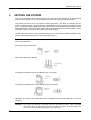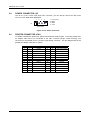
1
AR-B1320 User’s Guide
AR-B1320
PC/104 386SX CPU BOARD
User’s Guide
Edition: 1.3
Book Number: AR-B1320-02.0725
I
AR-B1320 User’s Guide
Copyright Notice and Disclaimer
August 1999
This document is copyrighted, 1999, by Acrosser Technology Co., Ltd. All rights are reserved. No part of
this manual may be reproduced, copied, transcribed, stored in a retrieval system, or translated into any
language or computer language in any form or by any means, such as electronic, mechanical, magnetic,
optical, chemical, manual or other means without the prior written permission of original manufacturer.
Acrosser technology assumes no responsibility or warranty with respect to the contents in this manual and
specifically disclaims any implied warranties of merchantability or fitness for any particular purpose.
Furthermore, Acrosser Technology reserves the right to make improvements to the products described in
this manual at any times without notice. Such revisions will be posted on the Internet
(WWW.ACROSSER.COM) as soon as possible.
Possession, use, or copying of the software described in this publication is authorized only pursuant to a
valid written license from Acrosser or an authorized sub licensor.
Acknowledgements
(C) Copyright Acrosser Technology Co., Ltd., 1999. All rights Reserved.
Acrosser, Intel, ALI, AMI…are registered trademarks.
All other trademarks and registered trademarks are the property of their respective holders.
This document was produced with Adobe Acrobat 3.01.
2
II
AR-B1320 User’s Guide
Table of Contents
0.
PREFACE ............................................................................................................................................... V
0.1
0.2
0.3
0.4
0.5
0.6
1.
OVERVIEW.......................................................................................................................................... 1-1
1.1
1.2
1.3
2.
INTRODUCTION............................................................................................................................ 1-1
PACKING LIST............................................................................................................................... 1-1
FEATURES .................................................................................................................................... 1-2
SYSTEM CONTROLLER .................................................................................................................... 2-1
2.1
2.2
2.3
2.4
2.5
2.6
2.7
2.8
2.9
2.10
2.11
2.12
3.
WELCOME TO THE AR-B1320 CPU BOARD ................................................................................. V
BEFORE YOU USE THIS GUIDE..................................................................................................... V
RETURNING YOUR BOARD FOR SERVICE .................................................................................. V
TECHNICAL SUPPORT AND USER COMMENTS.......................................................................... V
ORGANIZATION .............................................................................................................................. VI
STATIC ELECTRICITY PRECAUTIONS......................................................................................... VI
MICROPROCESSOR .................................................................................................................... 2-1
DMA CONTROLLER...................................................................................................................... 2-1
DRAM CONFIGURATION ............................................................................................................. 2-2
I/O CONTROLLER ......................................................................................................................... 2-2
I/O PORT ADDRESS MAP ............................................................................................................ 2-3
INTERRUPT CONTROLLER ......................................................................................................... 2-4
SERIAL PORTS ............................................................................................................................. 2-5
PARALLEL PORT .......................................................................................................................... 2-7
TIMER ............................................................................................................................................ 2-9
REAL-TIME CLOCK AND NON-VOLATILE RAM.................................................................... 2-10
WATCHDOG TIMER ................................................................................................................ 2-11
FLASH DISK............................................................................................................................. 2-11
SETTING THE SYSTEM ..................................................................................................................... 3-1
3.1
3.2
3.3
3.4
3.5
3.6
3.7
3.8
3.9
3.10
3.11
BOARD LAYOUT ........................................................................................................................... 3-2
CPU BASE CLOCK SELECT (JP1) ............................................................................................... 3-4
SWITCH SETTINGS (SW1)........................................................................................................... 3-4
EXTERNAL LED HEADER (J1) ..................................................................................................... 3-4
KEYBOARD CONNECTOR (J2).................................................................................................... 3-5
RESET HEADER (J3) .................................................................................................................... 3-5
SPEAKER HEADER (J4) ............................................................................................................... 3-5
POWER CONNECTOR (J5) .......................................................................................................... 3-6
PRINTER CONNECTOR (CN1)..................................................................................................... 3-6
FLOPPY CONNECTOR (CN2)................................................................................................... 3-7
SERIAL PORT CONNECTORS (CN3, CN4 & CN5) ................................................................. 3-7
3.11.1
3.11.2
3.11.3
3.12
3.13
3.13.1
3.13.2
3.13.3
3.14
3.14.1
3.14.2
3.15
3.15.1
3.15.2
RS-232C Connectors (CN3 & CN4) .......................................................................................................3-8
RS-485 Connector (CN5) .......................................................................................................................3-8
RS-485 Terminator (JP2 & JP3).............................................................................................................3-9
HARD DISK CONTROLLER (CN6)............................................................................................ 3-9
PC/104 CONNECTOR (CN7 & CN8) ....................................................................................... 3-10
64 Pin PC/104 Connector – cn8 (Bus A & B) .......................................................................................3-10
40 Pin PC/104 Connector - CN7 (Bus C & D) ......................................................................................3-10
PC/104 Channel Signal Description .....................................................................................................3-11
LED INDICATOR (LED1 & LED2) ............................................................................................ 3-12
power led (led1) ...................................................................................................................................3-12
Status led (led2) ...................................................................................................................................3-12
USING THE WATCHDOG TIMER ........................................................................................... 3-13
WD enable register - INDEX 37H .........................................................................................................3-13
WD Report register - INDEX 38H .........................................................................................................3-14
III
AR-B1320 User’s Guide
3.15.3
3.15.4
3.15.5
3.16
USING THE FLASH DISK ........................................................................................................ 3-16
3.16.1
3.16.2
3.16.3
4.
SSD Configuration................................................................................................................................3-17
Software Programming.........................................................................................................................3-17
DiskOnModule......................................................................................................................................3-18
BIOS CONSOLE ................................................................................................................................. 4-1
4.1
4.2
4.3
4.4
4.5
4.6
4.7
4.8
BIOS SETUP OVERVIEW ............................................................................................................. 4-1
STANDARD CMOS SETUP........................................................................................................... 4-2
ADVANCED CMOS SETUP .......................................................................................................... 4-4
ADVANCED CHIPSET SETUP...................................................................................................... 4-7
PERIPHERAL SETUP ................................................................................................................... 4-9
AUTO-DETECT HARD DISKS..................................................................................................... 4-10
PASSWORD SETTING................................................................................................................ 4-10
SETTING THE PASSWORD ....................................................................................................... 4-10
4.8.1
4.9
4.10
Auto Configuration with Optimal Setting...............................................................................................4-11
Auto Configuration with Fail Safe Setting .............................................................................................4-11
BIOS EXIT ................................................................................................................................ 4-11
4.10.1
4.10.2
4.11
Checking the Password........................................................................................................................4-10
LOAD THE DEFAULT SETTING ................................................................................................. 4-11
4.9.1
4.9.2
5.
WD TIMER COUNTER(24 bits) - INDEX 39H, 3Ah, and 3bH ..............................................................3-14
Timeout Status & Reset Watchdog - INDEX 3CH ................................................................................3-15
Programming Watchdog - Basic Operation ..........................................................................................3-15
Save Settings and Exit .........................................................................................................................4-11
Exit Without Saving ..............................................................................................................................4-11
BIOS UPDATE ......................................................................................................................... 4-12
APPENDIX........................................................................................................................................... 5-1
5.1
5.2
5.3
5.4
SPECIFICATIONS ......................................................................................................................... 5-1
SUPPORTED FLASH MEMORY ................................................................................................... 5-2
BOARD DIMENSIONS................................................................................................................... 5-3
PROGRAMMING THE RS-485...................................................................................................... 5-4
4
IV
AR-B1320 User’s Guide
0.
PREFACE
0.1
WELCOME TO THE AR-B1320 CPU BOARD
This guide introduces the Acrosser AR-B1320 CPU board.
The following information provided in this manual describes this card’s functions and features. It
also helps you start, set up and operate your AR-B1320. General system information can also be
found in this publication.
0.2
BEFORE YOU USE THIS GUIDE
Please refer to Chapter 3, “Setting System,” in this guide, if you have not already installed ARB1320. Check the packing list before you install and make sure the accessories are completely
included.
The AR-B1320 CD provides the newest information regarding the CPU card. Please refer to the
files of the enclosed utility CD. It contains the modification, hardware & software information, and
it has updated to product functions that may not be mentioned here.
0.3
RETURNING YOUR BOARD FOR SERVICE
If your board requires any services, contact the distributor or sales representative from whom you
purchased the product for service information. If you need to ship your board to us for service, be
sure it is packed in a protective carton. We recommend that you keep the original shipping
container for this purpose.
You can help assure efficient servicing for your product by following these guidelines:
1). Include your name, address, daytime telephone, facsimile number and e-mail.
2). A description of the system configurations and/or the software at the time of malfunction.
3). A brief description of the problem occurred.
0.4
TECHNICAL SUPPORT AND USER COMMENTS
User's comments are always welcome as they assist us in improving the quality of our products and
the readability of our publications. They create a very important part of input used for product
enhancement and revision.
We may use and distribute any of the information you provide in any way appropriate without
incurring any obligation. You may, of course, continue to use the information you provide.
If you have any suggestions for improving particular sections or if you find any errors on it, please
send your comments to Acrosser Technology Co., Ltd. or your local sales representative and
indicate the manual title and book number.
Send Internet electronic mail to: [email protected]
V
AR-B1320 User’s Guide
0.5
ORGANIZATION
This information covers the following topics (see the Table of Contents for a detailed listing):
!
!
!
!
!
0.6
Chapter 1, “Overview,” provides an overview of the system features and packing list.
Chapter 2, “System Controller,” describes the major structure.
Chapter 3, “Setting the System,” describes how to adjust the jumpers, and the connector
settings.
Chapter 4, “BIOS Console,” providing the BIOS settings.
Appendix
# Specifications
# Supported flash memory
# Board dimensions
# Programming the RS-485
STATIC ELECTRICITY PRECAUTIONS
Before removing the board from its anti-static bag, read this section about the static electricity
precautions.
Static electricity is a constant danger to computer systems. The charge that can build up in your
body may be more than sufficient to damage integrated circuits on any PC board. It is, therefore,
important to observe basic precautions whenever you use or handle computer components.
Although areas with humid climates are much less prone to the static built up, it is always best to
safeguard against accidents, which may result in expensive repairs. The following measures
should generally be sufficient to protect your equipment from static discharge:
1)
2)
3)
Touch a grounded metal object to discharge the static electricity in your body (or ideally,
wear a grounded wrist strap).
When unpacking and handling the board or other system components, place all materials
on an antic-static surface.
Be careful not to touch the components on the board, especially the “gold finger”
connectors on the bottom of every board.
6
VI
AR-B1320 User’s Guide
1.
OVERVIEW
This chapter provides an overview of your system features and capabilities. The following topics
are covered:
!
!
!
1.1
Introduction
Packing List
Features
INTRODUCTION
The AR-B1320, PC/104 CPU module is a lower power consuming, high performance 386 based
computer. By using the space-saving features of the ALI M6117C CPU, this module is able to
support up to 4MB of DRAM and 1.5 MB of Flash memory on board. The unit also comes with
two RS-232C/RS-485 ports, 1 parallel port, 1 floppy interface, 1 IDE interface, and 1 DiskOnChip
socket for adding a high degree of versatility to any project. The AR-B1320 is an excellent choice
for mobile systems, or as a controller for machines that are too small to accommodate traditional
industrial PCs.
The AR-B1320 offers higher speed and it makes a very stable 386SX-based system with a true
PC/104 module for embedded applications.
This manual has been written to assist you in installing, configuring and running the AR-B1320
CPU card. Each section is intended to guide you through its procedures clearly and concisely,
allowing you to continue to the next chapters without any difficulty.
1.2
PACKING LIST
These accessories are included with the system. Before you begin installing your AR-B1320
board, take a moment to make sure that the following items have been included inside the ARB1320 package.
!
!
!
!
!
!
!
A quick setup guide
1 AR-B1320 PC/104 386SX CPU board
1 Floppy adapter cable
2 RS-232C interface cables
1 Printer adapter cable
1 Power adapter cable
1 Utility diskette
Accessory
Keyboard adapter cable
Floppy adapter cable
RS-232C interface cable
Printer adapter cable
Power adapter cable
Description
6-pin JST to 6-pin mini-din IBM PS/2 standard
type
16-pin mini-IDC to 34-pin IDC
10-pin IDC to DB-9 male
26-pin mini-IDC to DB-25 female
4-pin JST power cable
Table 1-1 Accessories
1-1
AR-B1320 User’s Guide
1.3
FEATURES
This system provides a number of special features that enhance its reliability, ensure its
availability, and improve its expansion capabilities, as well as its hardware structure.
!
!
!
!
!
!
!
!
!
!
!
!
!
!
!
!
1-2
80386SX-40 MHz CPU
PC/104 extension bus
System of up to 4MB DRAM (2 MB already on-board)
Supports 2 RS-232C/RS-485 serial ports
PC/AT compatible keyboard interface
Supports up to 1.5MB flash disk
Programmable watchdog timer
Flash BIOS
Supports two IDE drives
Supports one floppy drive
Supports one SPP/EPP/ECP printer port
Supports DiskOnChip and DiskOnModule
Powered-on LED indicator
Signal 5V power requirement
Multi-layer PCB for noise reduction
Dimensions: 90.2mmX95.9mm (3.55”x3.775”)
AR-B1320 User’s Guide
2.
SYSTEM CONTROLLER
This chapter describes the major structure. The following topics are covered:
!
!
!
!
!
!
!
!
!
!
!
2.1
Microprocessor
DMA Controller
DRAM Configuration
I/O Port Address Map
Interrupt Controller
Serial Port
Parallel Port
Timer
Real-Time Clock and Non-Volatile RAM
Watch-Dog Timer
FLASH Disk
MICROPROCESSOR
The AR-B1320 uses the ALI M6117C CPU; it is designed to perform like Intel’s 386SX-based
system with deep green features.
The 386SX core is the same as M1386SX of Acer Labs. Inc. and 100% object code compatible
with the Intel 386SX microprocessor. System manufacturers can provide 386 CPU based
systems optimized for both cost and size. Instruction pipelining and high bus bandwidth ensure
short average instruction-execution times and high system throughput. Furthermore, it can keep
the state internally from charge leakage while external clock to the core is stopped without storing
the data in registers. The power consumption here is almost zero when the clock stops. The
internal structure of this core is 32-bit and its address bus has a very low supply current. The real
mode as well as the protected mode are available and can run MS-DOS, MS-Windows, OS/2 and
UNIX.
2.2
DMA CONTROLLER
The equivalent of two 8237A DMA controllers are implemented in the AR-B1320 card. Each
controller is a four-channel DMA device, which will generate the memory addresses and control
signals necessary to transfer information directly between a peripheral device and memory. This
allows high-speed information transfer with less CPU intervention. The two DMA controllers are
internally cascaded to provide four DMA channels for transfers to 8-bit peripherals (DMA1) and
three channels for transfers to 16-bit peripherals (DMA2). DMA2 channel 0 provides the cascade
interconnection between the two DMA devices, thereby maintaining the IBM PC/AT compatibility.
The following is the DMA channels:
DMA Controller 1
DMA Controller 2
Channel 0: Spare
Channel 1: IBM SDLC
Channel 2: Diskette adapter
Channel 3: Spare
Channel 4: Cascade for controller 1
Channel 5: Spare
Channel 6: Spare
Channel 7: Spare
Table 2-1 DMA Channel Controller
2-1
AR-B1320 User’s Guide
2.3
DRAM CONFIGURATION
There are two 16-bit memory banks on the AR-B1320 board. The first bank is embedded with a
1MBx16-bit (2MB, 60ns) EDO RAM and the other is 42-pin SOJ socket for extra 2MB DRAM with
1MBx16-bit (2MB, 60ns) EDO RAM. Please refer to the following table for details:
U15 (On-Board)
EDO 1Mx16
EDO 1Mx16
2.4
U1 (Socket)
None
EDO 1Mx16
Total Memory
2MB
4MB
Remark
Factory Preset
I/O CONTROLLER
A super I/O chip (SMC37C669) is embedded at the back panel of the AR-B1320 board. It
combines the functions of a floppy disk drive adapter, a hard disk drive (IDE) adapter, two serial
(with 16C550 UART) adapters and 1 parallel adapter. Setting the BIOS setup program can do the
I/O port configurations.
As a UART, the chip supports the serial to parallel conversion on data characters received from a
peripheral device or a MODEM, and the parallel to serial conversion on data character received
from the CPU. The UART includes a programmable baud rate generator; complete MODEM
control capability and a processor interrupt system. For the parallel port, the SMC37C669
provides the user with a fully bi-directional centronics-type printer interface.
2-2
AR-B1320 User’s Guide
2.5
I/O PORT ADDRESS MAP
Hex Range
Device
Factory Preset
000-01F
DMA controller 1
✓
020-021
Interrupt controller 1
✓
022-023
ALI M6117C chipset address
✓
040-04F
Timer 1
✓
050-05F
Timer 2
✓
060-06F
8042 keyboard/controller
✓
✓
070-071 Real-time clock (RTC), non-maskable interrupt
(NMI)
080-09F
DMA page registers
✓
0A0-0A1
Interrupt controller 2
✓
0C0-0DF
DMA controller 2
✓
0F0
Clear Math Co-processor
0F1
Reset Math Co-processor
0F8-0FF
Math Co-processor
170-178
Fixed disk 1
1F0-1F8
Fixed disk 0
✓
201
Game port
208-20A
EMS register 0
218-21A
EMS register 1
278-27F
Parallel printer port 3 (LPT 3)
2E8-2EF
Serial port 4 (COM 4)
2F8-2FF
Serial port 2 (COM 2)
✓
300-31F
Prototype card/Streaming Type Adapter
378-37F
Parallel printer port 2 (LPT 2)
✓
380-38F
SDLC, bisynchronous
3A0-3AF
Bisynchronous
3B0-3BF
Monochrome display and printer port 1 (LPT
1)
3C0-3CF
EGA/VGA adapter
3D0-3DF
Color/Graphics monitor adapter
3E8-3EF
Serial port 3 (COM 3)
3F0-3F7
Diskette controller
3F8-3FF
Serial port 1 (COM 1)
Table 2-2 I/O Port Address Map
Note: The I/O port address with the mark “✓” means that they are the BIOS CMOS default values. You can configure your
own settings according to this address map.
2-3
AR-B1320 User’s Guide
2.6
INTERRUPT CONTROLLER
The ALI M6117C also provides two-cascaded 8259 Programmable Interrupt Controllers (PIC). They
accept requests from the peripherals, resolve priorities on pending interrupts in service, issue
interrupt requests to the CPU, and provide vectors which are used as acceptance indexed by the
CPU to determine which interrupt service routine should be executed.
The following is the system information of interrupts levels:
Interrupt Level
In
Description
NMI
Parity check
CTRL1
IRQ 0
IRQ 1
IRQ 2
CTRL2
System timer interrupt from timer 8254
Keyboard output buffer full
IRQ8 : Real time clock
IRQ9 : Rerouting to INT 0Ah from hardware IRQ2
IRQ10 : Spare
IRQ11 : Spare
IRQ12 : Spare
IRQ13 : Reserved for Math. coprocessor
IRQ14 : Hard disk adapter
IRQ15 : Spare
IRQ 3
IRQ 4
IRQ 5
IRQ 6
IRQ 7
Serial port 2
Serial port 1
Spare
Floppy disk
Parallel
d
4port
Figure 2-1 Interrupt Controller
2-4
AR-B1320 User’s Guide
2.7
SERIAL PORTS
The ACEs (Asynchronous Communication Elements ACE1 and ACE2) are used to convert the
parallel data to a serial format on the transmit side and convert the serial data to parallel on the
receiver side. The serial format, in order of transmission and reception, is a start bit, followed by
five to eight data bits, a parity bit (if programmed) and one, one and half (five-bit format only) or
two stop bits. The ACEs are capable of handling divisors of 1 to 65535, and produce a 16x clock
for driving the internal transmitter logic.
Provisions are also included to use this 16x clock to drive the receiver logic. Also included in the
ACE are a complete MODEM control capability, and a processor interrupt system that may be
software tailored to the computing time required to handle the communications link. The following
is a summary of each ACE accessible registers.
DLAB
0
Port Address
base + 0
0
X
X
X
X
X
X
1
1
base + 1
base + 2
base + 3
base + 4
base + 5
base + 6
base + 7
base + 0
base + 1
Register
Receiver buffer (RBR, read)
Transmitter holding register (THR, write)
Interrupt enable (IER)
Interrupt identification (IIR, read only)
Line control (LCR)
MODEM control (MCR)
Line status (LSR)
MODEM status (MSR)
Scratched register
Divisor latch (least significant byte) (LS)
Divisor latch (most significant byte) (MS)
Table 2-3 ACE Accessible Register
(1)
Receiver Buffer Register (RBR)
Bit 0-7: Received data byte (Read Only)
(2)
Transmitter Holding Register (THR)
Bit 0-7: Transmitter holding data byte (Write Only)
(3)
Interrupt Enable Register (IER)
Bit 0: Enable Received Data Available Interrupt (ERBFI)
Bit 1: Enable Transmitter Holding Empty Interrupt (ETBEI)
Bit 2: Enable Receiver Line Status Interrupt (ELSI)
Bit 3: Enable MODEM Status Interrupt (EDSSI)
Bit 4: Must be 0
Bit 5: Must be 0
Bit 6: Must be 0
Bit 7: Must be 0
(4)
Interrupt Identification Register (IIR)
Bit 0: “0” if Interrupt Pending
Bit 1: Interrupt ID Bit 0
Bit 2: Interrupt ID Bit 1
Bit 3: Must be 0
Bit 4: Must be 0
Bit 5: Must be 0
Bit 6: Must be 0
Bit 7: Must be 0
2-5
AR-B1320 User’s Guide
(5)
Line Control Register (LCR)
Bit 0: Word Length Select Bit 0 (WLS0)
Bit 1: Word Length Select Bit 1 (WLS1)
WLS1
0
0
1
1
WLS0
0
1
0
1
Word Length
5 Bits
6 Bits
7 Bits
8 Bits
Bit 2: Number of Stop Bit (STB)
Bit 3: Parity Enable (PEN)
Bit 4: Even Parity Select (EPS)
Bit 5: Stick Parity
Bit 6: Set Break
Bit 7: Divisor Latch Access Bit (DLAB)
(6)
MODEM Control Register (MCR)
Bit 0: Data Terminal Ready (DTR)
Bit 1: Request to Send (RTS)
Bit 2: Out 1 (OUT 1)
Bit 3: Out 2 (OUT 2)
Bit 4: Loop
Bit 5: Must be 0
Bit 6: Must be 0
Bit 7: Must be 0
(7)
Line Status Register (LSR)
Bit 0: Data Ready (DR)
Bit 1: Overrun Error (OR)
Bit 2: Parity Error (PE)
Bit 3: Framing Error (FE)
Bit 4: Break Interrupt (BI)
Bit 5: Transmitter Holding Register Empty (THRE)
Bit 6: Transmitter Shift Register Empty (TSRE)
Bit 7: Must be 0
(8)
MODEM Status Register (MSR)
Bit 0: Delta Clear to Send (DCTS)
Bit 1: Delta Data Set Ready (DDSR)
Bit 2: Training Edge Ring Indicator (TERI)
Bit 3: Delta Receive Line Signal Detect (DSLSD)
Bit 4: Clear to Send (CTS)
Bit 5: Data Set Ready (DSR)
Bit 6: Ring Indicator (RI)
Bit 7: Received Line Signal Detect (RSLD)
2-6
AR-B1320 User’s Guide
(9)
Divisor Latch (LS, MS)
Byte Data
Bit 0:
Bit 1:
Bit 2:
Bit 3:
Bit 4:
Bit 5:
Bit 6:
Bit 7:
Desired
Baud Rate
50
75
110
134.5
150
300
600
1200
1800
2000
2400
3600
4800
7200
9600
14400
19200
28800
38400
57600
115200
LS
Bit 0
Bit 1
Bit 2
Bit 3
Bit 4
Bit 5
Bit 6
Bit 7
MS
Bit 8
Bit 9
Bit 10
Bit 11
Bit 12
Bit 13
Bit 14
Bit 15
Divisor Used to
Present Error Difference
Generate 16x Clock Between Desired and Actual
2304
--1536
--1047
0.026
857
0.058
768
--384
--192
--96
--64
--58
0.69
48
--32
--24
--16
--12
--8
--6
--4
--3
--2
--1
--Table 2-4 Serial Port Divisor Latch
2.8
PARALLEL PORT
(1) Register Address
Port Address
base+0
base+0
base+1
base+2
Read/Write
Write
Read
Read
Write
Register
Output data
Input data
Printer status buffer
Printer control latch
(2) Printer Interface Logic
The parallel portion of the SMC37C669 makes the attachment of various devices that accept
eight bits of parallel data at standard TTL level.
2-7
AR-B1320 User’s Guide
(3) Data Swapper
The system microprocessor can read the contents of the printer's Data Latch through the
Data Swapper by reading the Data Swapper address.
(4) Printer Status Buffer
The system microprocessor can read the printer status by reading the address of the Printer
Status Buffer. The bit definitions are described as follows:
7
6
5
4
3
2
1
0
X
X
X
-ERROR
SLCT
PE
-ACK
-BUSY
Bit 7: This signal may become active during data entry, when the printer is off-line during
printing, or when the print head is changing position or in an error state. When Bit 7 is
active, the printer is busy and cannot accept data.
Bit 6: This bit represents the current state of the printer's ACK signal. A 0 means the printer
has received the character and is ready to accept another. Normally, this signal will be
active for approximately 5 microseconds before BUSY stops.
Bit 5: A 1 means the printer has detected the end of paper.
Bit 4: A 1 means the printer is selected.
Bit 3: A 0 means the printer has encountered an error condition.
Bit 0-2: No meaning.
(5) Printer Control Latch & Printer Control Swapper
The system microprocessor can read the contents of the printer control latch by reading the
address of printer control swapper. Bit definitions are as follows:
7
6
X
X
5
4
3
2
1
0
STROBE
AUTO FD XT
INIT
SLDC IN
IRQ ENABLE
DIR(write only)
Bit 5: Direction control bit. When logic 1, the output buffers in the parallel port are disabled
allowing data driven from external sources to be read; when logic 0, they work as a
printer port. This bit is writing only.
Bit 4: A 1 in this position allows an interrupt to occur when ACK changes from low state to
high state.
Bit 3: A 1 in this bit position selects the printer.
Bit 2: A 0 starts the printer (50μsecond pulse, minimum).
Bit 1: A 1 causes the printer to line-feed after a line is printed.
Bit 0: A 0.5μsecond minimum high active pulse clocks data into the printer. Valid data must
be present for a minimum of 0.5μseconds before and after the strobe pulse.
2-8
AR-B1320 User’s Guide
2.9
TIMER
The AR-B1320 provides three programmable timers, each with a timing frequency of 1.19 MHz.
Timer 0 The output of this timer is tied to interrupt request 0. (IRQ 0)
Timer 1 This timer is used to trigger memory refresh cycles.
Timer 2 This timer provides the speaker tone.
Application programs can load different counts into this timer to
generate various sound frequencies.
2-9
AR-B1320 User’s Guide
2.10
REAL-TIME CLOCK AND NON-VOLATILE RAM
The AR-B1320 contains a real-time clock compartment that maintains the date and time in
addition to storing configuration information about the computer system. It contains 14 bytes of
clock and registers and 114 bytes of general purpose RAM. Because of the use of CMOS
technology, it consumes very little power and can be maintained for long periods of time using an
internal lithium battery.
Address
00
01
02
03
04
05
06
07
08
09
0A
0B
0C
0D
0E
0F
10
11
12
13
14
15
16
17
18
19-2D
2E-2F
30
31
32
33
34-7F
Description
Seconds
Second alarm
Minutes
Minute alarm
Hours
Hour alarm
Day of week
Date of month
Month
Year
Status register A
Status register B
Status register C
Status register D
Diagnostic status byte
Shutdown status byte
Diskette drive type byte, drive A and B
Fixed disk type byte, drive C
Fixed disk type byte, drive D
Reserved
Equipment byte
Low base memory byte
High base memory byte
Low expansion memory byte
High expansion memory byte
Reserved
2-byte CMOS checksum
Low actual expansion memory byte
High actual expansion memory byte
Date century byte
Information flags (set during power on)
Reserved for system BIOS
Table 2-5 Real-Time Clock & Non-Volatile RAM
2-10
AR-B1320 User’s Guide
2.11
WATCHDOG TIMER
The AR-B1320 is equipped with a programmable time-out period watchdog timer. Actually, the
watchdog timer is provided by the ALI M6117C chipset. You can use the program to enable the
watchdog timer. Once you have enabled the watchdog timer, the program should trigger it every
time before it times out. If your program fails to disable this timer before it times out because of a
system hang-up, it will generate a reset signal to reset the system or trigger an IRQ or NMI signal
to tell your program that the watchdog has timed out. The time-out period can be programmed to
be 30.5μseconds to 512 seconds with 30.5μseconds per step.
2.12
FLASH DISK
The AR-B1320 supports three kinds of flash disks. They are Acrosser’s SSD, DiskOnChip, and
DiskOnModule. For the SSD, AR-B1320 provides two 32-pin PLCC sockets and 1 32-pin
JEDEC DIP socket, which may be populated with up to 1.5MB of flash disk. The 32-pin JEDEC
DIP socket supports the DiskOnChip from 2MB to 144MB. The DiskOnModule is connected to
the onboard IDE connector. All the flash disks are ideal for diskless systems, and are also highly
reliable for high-speed access applications, as controllers for industrial use, or line test
instruments, etc.
2-11
AR-B1320 User’s Guide
3.
SETTING THE SYSTEM
This section describes the pin assignments of all connectors and settings of all switches and
jumpers. It also guides you on how to expand the system and control the onboard devices.
The jumper pins allow you to set specific system parameters. Set them by changing the pin
location of jumper blocks. (A jumper block is a small plastic-encased conductor that slips over the
pins.) To change a jumper setting, remove the jumper from its current location with your fingers or small
needle-nosed pliers. Place the jumper over the two pins designated for the desired setting. Press
the jumper evenly onto the pins. Be careful not to bend the pins.
We will show the locations of the AR-B1320 jumper pins, and the factory-default settings in this
section. Note that the square pin of each jumper block is pin 1.
Below illustrates the jumper use. Jumper caps are usually small plastic caps used to short two
pins on a jumper block.
Most jumper caps look like this:
A Jumper
C
Most jumper blocks look like this:
A 3 Pin jumper
Block
If the jumper is placed over pins one and two then 1-2 are ON.
Jumper on
Pins1 + 2
If the jumper is placed over pins two and three then 2-3 are ON.
Jumper On
Pins 2 + 3
Otherwise, the jumper can be left to the side or completely off the block to keep both 1-2 and 2-3
off (open).
CAUTION:
Do not touch any electronic component unless you are safely grounded. Wear a grounded
wrist strap or touch an exposed metal part of the system unit chassis. Static discharges from
your fingers can permanently damage electronic components.
3-1
AR-B1320 User’s Guide
3.1
BOARD LAYOUT
The AR-B1320 is a small, easy to use, all-in-one 386SX grade CPU board with 2 RS-232/RS-485
ports and a flash disk. Below is the AR-B1320 board layout.
CN1
CN2
2
1
1
CN3
U2
[M1]
2
2
U3
BIOS
6
OFF
U5
[M2]
1
J3
J4
CN6
2
U12
2
SSD/DOC
1
J3
J4
SW1
1
CN5
J1
U1
12 34 56
2
CN4
J1
STS
4
1
CN5
PWR
44 43
JP1
JP1
JP2
JP2
JP3
JP3
16
15
2
CN3
1
CN4
LED1 LED2
2
1
2
1
J2
1
CN8
2
64
1
63
J5
1
1
39
2
40
AR-B1320 VER:1.1
CN7
Figure 3-1 AR-B1320 Board Layout
3-2
1
[M3]
AR-B1320 User’s Guide
Name
JP1
JP2
JP3
SW1
J1
J2
J3
J4
J5
CN1
CN2
CN3
CN4
CN5
CN6
CN7
CN8
LED1
LED2
U1
U2
U5
U12
Function
CPU base clock select
RS-485 terminator select (COM-A)
RS-485 terminator select (COM-B)
Switch 1
The base I/O address of SSD selector
Switch 2
The memory segment of SSD selector
Switch 3
The memory segment of DiskOnChip selector
Switch 4
Reserved
Switch 5
COM-A port mode selector
Switch 6
COM-B port mode selector
External power and hard disk LED header
Keyboard connector
Reset header
Speaker header
Power connector
Printer connector
Floppy connector
RS-232C connector (COM-A)
RS-232C connector (COM-B)
RS-485 connector
44-pin IDE connector
40-pin PC/104 connector (Bus C & D)
64-pin PC/104 connector (Bus A & B)
Onboard power LED
User defined status LED
Expandable DRAM socket
Flash socket (First)
Flash socket (Second)
Flash socket (Third) and DiskOnChip socket
Section
3.2
3.11.3
3.11.3
3.3
3.3
3.3
3.3
3.3
3.3
3.4
3.5
3.6
3.7
3.8
3.9
3.10
3.11
3.11
3.11
3.12
3.13.2
3.13.1
3.14.1
3.14.2
2.3
3.16
3.16
3.16
Table 3-1 Important Component List
3-3
AR-B1320 User’s Guide
3.2
CPU BASE CLOCK SELECT (JP1)
This board provides six types of CPU input clocks; they are 33.3MHz, 50MHz, 60MHz, 66.7MHz,
75MHz, and 80MHz. The CPU input clock is twice that of the operating clock. JP1 is a 6-pin
jumper located between CN3 and CN4.
CPU Input Clock
CPU Operating Clock
JP1 Setting
33.3MHz
16.7MHz
Short 1-2 & 4-6
50MHz
25MHz
Short 1-2 & 3-5
60MHz
30MHz
Short 1-2 & 5-6
66.7MHz
33.3MHz
Short 1-3 & 5-6
75MHz
37.5MHz
Short 2-4 & 5-6
40MHz
Short 1-3 & 2-4
80MHz
Remark
Factory Preset
Table 3-2 CPU Clock Settings
JP1
JP1
JP1
JP1
JP1
JP1
1
2
1
2
1
2
1
2
1
2
1
2
3
4
3
4
3
4
3
4
3
4
3
4
5
6
5
6
5
6
5
6
5
6
5
6
16.7MHz
25MHz
30MHz
33.3MHz
37.5MHz
40MHz
Figure 3-2 JP1: CPU Clock Select
3.3
SWITCH SETTINGS (SW1)
SW1 is a 6-SPST DIP switch. It provides multi-purpose selection in one switch. The following
table gives the details:
SW1
Function
When “OFF”
When “ON”
Factory Preset
Switch 1
Selects the base I/O address of SSD
210H-211H
290H-291H
Off
Switch 2
Selects the memory segment of SSD
Switch 2 Selects the memory segment of DiskOnChip
(If Switch 3 is set as “ON”)
C800H(8KB)
D800H(8KB)
Off
CA00H(8KB)
DA00H(8KB)
Off
Switch 3
DiskOnChip select
Disabled
Enabled
Off
Switch 4
Reserved
---
---
Off
Switch 5
COM-A port mode select
RS-232C
RS-485
Off
Switch 6
COM-B port mode select
RS-232C
RS-485
Off
Table 3-3 SW1 Settings
3.4
EXTERNAL LED HEADER (J1)
The J1 is a 4-pin right angle header. It allows you to connect an external power LED and an
external hard disk LED.
J1
2
4
1
3
1: Power LED+
3: Power LED2: Hard Disk LED+
4: Hard Disk LED-
Front View
Figure 3-3 J1: External LED Header
3-4
AR-B1320 User’s Guide
3.5
KEYBOARD CONNECTOR (J2)
The J2 is a 6-pin 2.0mm JST connector. Use the keyboard adapter cable to connect a PS/2 type
keyboard. The following shows the pin assignment of the adapter cable.
J2
1 Reserved
2 KB Data
3 GND
4 VCC
5 Reserved
6 KB Clock
6 Pin Mini-Din
1
2
1
3
2
3
4
5
5
6
1
2
4
3
6 4
5
6
DATA
N.C.
GND
VCC
CLOCK
N.C.
Figure 3-4 J2: Keyboard Connector
3.6
RESET HEADER (J3)
The J3 is used to connect to an external reset switch. Shorting these two pins will reset the
system.
J3
2
1: Reset+
2: Reset-
1
Front View
Figure 3-5 J3: Reset Header
3.7
SPEAKER HEADER (J4)
The AR-B1320 provides a 2-pin right angle header for connecting an external speaker.
J4
2
1
1: Speaker+
2: Speaker-
Front View
Figure 3-6 J4: Speaker Header
Note: J3 and J4 are next to each other. Please notice their orientation and pin locations when you
are installing the system.
3-5
AR-B1320 User’s Guide
3.8
POWER CONNECTOR (J5)
The J5 is a 4-pin, 2.5mm, right angle JST connector; you can directly connect the DC power
source to J5 for stand-alone applications.
1
2
3
4
1: VCC (+5V)
2: GND
3: GND
4: +12V
J5
Front View
Figure 3-7 J5: Power Connector
3.9
PRINTER CONNECTOR (CN1)
To enable or disable the printer port, please use the BIOS setup program. To use the parallel port,
an adapter cable has to be connected to the CN1 connector (26-pin 2.0mm housing). The
connector for the parallel port is a 25 pin D-type female connector. The pin assignments for the
parallel port adapter cable are as follows:
CN1
1
3
5
7
9
11
13
15
17
19
21
23
25
DB25
1
2
3
4
5
6
7
8
9
10
11
12
13
Decryption
-Strobe
Data 0
Data 1
Data 2
Data 3
Data 4
Data 5
Data 6
Data 7
-Acknowledge
Busy
Paper Empty
Printer Select
CN1
2
4
6
8
10
12
14
16
18
20
22
24
26
DB25
14
15
16
17
18
19
20
21
22
23
24
25
----
Decryption
-Auto Form Feed
-Error
-Initialize
-Printer Select In
Ground
Ground
Ground
Ground
Ground
Ground
Ground
Ground
No Connect
Table 3-4 The Printer Adapter Cable Pin Assignments
3-6
AR-B1320 User’s Guide
3.10
FLOPPY CONNECTOR (CN2)
The AR-B1320 provides a 16-pin 2.0mm connector (CN2) to support one floppy disk drive. The
floppy drives may be one of the following:
•
•
5.25"
: 360K or 1.2M
3.5"
: 720K or 1.44M
To enable or disable the floppy disk controller, please use the BIOS Setup program. A floppy
adapter cable is used to connect between the CN2 connector (16-pin 2.0mm housing) and the
floppy disk drive. The following table illustrates the pin assignments of the floppy adapter cable.
CN2
34-PIN (Floppy Disk Drive)
Function
5,11,16
1,3,5,7, 17, 27, 31, 33
Ground
1
2
-Reduce write current
2
8
-Index
4
16
-Motor enable A
3
12
-Drive select A
6
18
-Direction
7
20
-Step output pulse
8
22
-Write data
9
24
-Write enable
10
26
-Track 0
12
28
-Write protect
13
30
-Read data
14
32
-Side 1 select
15
34
-Disk change
---
Else
No Connect
Table 3-5 Floppy Adapter Cable Pin Assignments
3.11
SERIAL PORT CONNECTORS (CN3, CN4 & CN5)
These 3 connectors serve the RS-232C/RS-485 of the COM-A port and the COM-B port.
•
•
•
CN3
: RS-232C connector for the COM-A port
CN4
: RS-232C connector for the COM-B port
CN5
: RS-485 connector for the COM-A and COM-B
Before you connect the serial port connectors, please refer to section 3.3 on how to set the switch
5 & 6 on SW1 for your desired use.
ON
OFF
1
2
3
4
5
6
Figure 3-8 SW1-5 & 6 –RS-232/RS-485 Select
3-7
AR-B1320 User’s Guide
3.11.1
RS-232C CONNECTORS (CN3 & CN4)
CN3 is the RS-232C- interface connector of COM-A port and CN4 is the RS-232C connector for
the COM-B port. They are both 10-pin 2.54mm right angle headers. AR-B1320 provides 2
adapter cables to transfer to the PC/AT standard connector (DB9 male). The next figure and table
show the pin definitions of the adapter cable:
2
10
1
9
1
5
CN3 &
CN4
6
Front View
9
DB9 Male
Figure 3-9 CN3 & CN4: RS-232C Connector
CN3 & CN4
Function
DB9 Male
Pin 1
-DCD
Pin 1
Pin 2
-DSR
Pin 6
Pin 3
RXD
Pin 2
Pin 4
-RTS
Pin 7
Pin 5
TXD
Pin 3
Pin 6
-CTS
Pin 8
Pin 7
-DTR
Pin 4
Pin 8
-RI
Pin 9
Pin 9
GND
Pin 5
Pin 10
Case Ground
Case
Table 3-6 CN3 & CN4 Pin Assignments
3.11.2
RS-485 CONNECTOR (CN5)
CN5 is used to connect the RS-485 interface of COM-A port and COM-B port.
assignments are shown below.
2
6
1
5
Front View
1: 485+ (COM-A)
3: 485- (COM-A)
5: Case Ground (COM-A)
2: 485+ (COM-B)
4: 485- (COM-B)
6: Case Ground (COM-B)
Figure 3-10 CN5: RS-485 Connector
3-8
It’s pin
AR-B1320 User’s Guide
3.11.3
RS-485 TERMINATOR (JP2 & JP3)
JP2 & JP3 are used to enable the RS-485 terminator resistor of COM-A and COM-B port
respectively. The value of the terminator resistor is 150 ohms. Close the jumper to enable the
RS-485 terminator and leave the jumper open to disable it.
COM Port
Jumper
When “Open”
When “Close”
Factory Preset
COM-A
JP2
Disabled
Enabled
Open
COM-B
JP3
Disabled
Enabled
Open
Table 3-7 JP2 & JP3: RS-485 Terminator
3.12
HARD DISK CONTROLLER (CN6)
A 44-pin header type connector (CN6) is provided to interface with up to two embedded hard disk
drives (IDE AT bus). This interface, through a 44-pin cable, allows the user to connect up to two
drives in a "daisy-chain" fashion. To enable or disable the hard disk controller, please use the
BIOS Setup program. The following table illustrates the pin assignments of the hard disk drive's
44-pin connector.
Pin
Function
Pin
Function
1
-Reset
2
Ground
3
Data 7
4
Data 8
5
Data 6
6
Data 9
7
Data 5
8
Data 10
9
Data 4
10
Data 11
11
Data 3
12
Data 12
13
Data 2
14
Data 13
15
Data 1
16
Data 14
17
Data 0
18
Data 15
19
Ground
20
Not used
21
Not used
22
Ground
23
-IOW
24
Ground
Ground
25
-IOR
26
27
Not used
28
BALE
29
Not used
30
Ground
31
IRQ 14
32
-IOCS16
33
SA1
34
Not used
35
SA0
36
SA2
37
-CS0
38
-CS1
39
Hard disk LED
40
Ground
41
VCC (+5V)
42
VCC (+5V)
Ground
44
Not used.
43
Table 3-8 CN6: IDE Connector
3-9
AR-B1320 User’s Guide
3.13
PC/104 CONNECTOR (CN7 & CN8)
The AR-B1320 CPU board has the stack-through expandable feature. You may stack a PC/104
module from either the backside or front side of this board through the PC-104 connector.
3.13.1
64 PIN PC/104 CONNECTOR – CN8 (BUS A & B)
CN8
1
-IOCHCK --SD7 --SD6 --SD5 --SD4 --SD3 --SD2 --SD1 --SD0 ---IORDY--AEN --SA19 --SA18 --SA17 --SA16 --SA15 --SA14 --SA13 --SA12 --SA11 --SA10 --SA9 --SA8 --SA7 --SA6 --SA5 --SA4 --SA3 --SA2 --SA1 --SA0 --GND ---
2
A1
A2
A3
A4
A5
A6
A7
A8
A9
A10
A11
A12
A13
A14
A15
A16
A17
A18
A19
A20
A21
A22
A23
A24
A25
A26
A27
A28
A29
A30
A31
A32
B1
B2
B3
B4
B5
B6
B7
B8
B9
B10
B11
B12
B13
B14
B15
B16
B17
B18
B19
B20
B21
B22
B23
B24
B25
B26
B27
B28
B29
B30
B31
B32
--- GND
--- RSTDRV
--- +5 VDC
--- IRQ9
--- Not Used
--- DRQ2
--- Not Used
--- ZWS
--- +12 VDC
--- Not Used
--- -MEMW
--- -MEMR
--- -IOW
--- -IOR
--- -DACK3
--- DRQ3
--- -DACK1
--- DRQ1
--- -REFRESH
--- BUSCLK
--- IRQ7
--- IRQ6
--- IRQ5
--- IRQ4
--- IRQ3
--- -DACK2
--- TC
--- BALE
--- +5 VDC
--- OSC
--- GND
--- GND
Figure 3-11 CN8: 64-Pin PC/104 Connector (Bus A & B)
3.13.2
40 PIN PC/104 CONNECTOR - CN7 (BUS C & D)
CN7
1
GND ---SBHE --LA23 --LA22 --LA21 --LA20 --LA19 --LA18 --LA17 ---MRD16 ---MWR16 --SD8 --SD9 --SD10 --SD11 --SD12 --SD13 --SD14 --SD15 --Not Used ---
C1
C2
C3
C4
C5
C6
C7
C8
C9
C10
C11
C12
C13
C14
C15
C16
C17
C18
C19
C20
2
D1
D2
D3
D4
D5
D6
D7
D8
D9
D10
D11
D12
D13
D14
D15
D16
D17
D18
D19
D20
--- GND
--- -MEM16
--- -IO16
--- IRQ10
--- IRQ11
--- IRQ12
--- IRQ15
--- IRQ14
--- -DACK0
--- DRQ0
--- -DACK5
--- DRQ5
--- -DACK6
--- DRQ6
--- -DACK7
--- DRQ7
--- +5 VDC
--- -MASTER
--- GND
--- GND
Figure 3- CN7: 40-Pin PC/104 Connector (Bus C & D)
3-10
AR-B1320 User’s Guide
3.13.3
PC/104 CHANNEL SIGNAL DESCRIPTION
Name
I/O
Description
BUSCLK
[Output]
The BUSCLK signal of the I/O channel is asynchronous to the CPU clock.
RSTDRV
[Output]
This signal goes high during power-up, low line-voltage or hardware reset
SA0 – SA19
[Input / Output]
The System Address lines run from bit 0 to 19. They are latched onto the falling
edge of "BALE"
LA17 - LA23
[Input / Output]
The Unlatched Address line run from bit 17 to 23
SD0 - SD15
[Input / Output]
System Data bit 0 to 15
BALE
[Output]
The Buffered Address Latch Enable is used to latch SA0 - SA19 onto the falling
edge. This signal is forced high during DMA cycles
-IOCHCK
[Input]
The I/O Channel Check is an active low signal which indicates that a parity error
exist on the I/O board
IOCHRDY
[Input, Open collector]
This signal lengthens the I/O, or memory read/write cycle, and should be held low
with a valid address
IRQ 3-7, 9-12,
14, 15
[Input]
The Interrupt Request signal indicates I/O service request attention. They are
prioritized in the following sequence : (Highest) IRQ 9, 10, 11, 12, 13, 15, 3, 4, 5,
6, 7 (Lowest)
-IOR
[Input / Output]
The I/O Read signal is an active low signal which instructs the I/O device to drive
its data onto the data bus
-IOW
[Input / Output]
The I/O write signal is an active low signal which instructs the I/O device to read
data from the data bus
-SMEMR
[Output]
The System Memory Read is low while any of the low 1 Mbytes of memory are
being used
-MEMR
[Input / Output]
The Memory Read signal is low while any memory location is being read
-SMEMW
[Output]
The System Memory Write is low while any of the low 1 Mbytes of memory is
being written
-MEMW
[Input / Output]
The Memory Write signal is low while any memory location is being written
DRQ 0-3, 5-7
[Input]
DMA Request channels 0 to 3 are for 8-bit data transfers. DMA Request channels
5 to 7 are for 16-bit data transfers. DMA request should be held high until the
corresponding DMA has been completed. DMA request priority is in the following
sequence:(Highest) DRQ 0, 1, 2, 3, 5, 6, 7 (Lowest)
-DACK 0-3, 5-7 [Output]
The DMA Acknowledges 0 to 3, 5 to 7 are the corresponding acknowledge signals
for DRQ 0 to 3 and 5 to 7
AEN
[Output]
The DMA Address Enable is high when the DMA controller is driving the address
bus. It is low when the CPU is driving the address bus
-REFRESH
[Input / Output]
This signal is used to indicate a memory refresh cycle and can be driven by the
microprocessor on the I/O channel
TC
[Output]
Terminal Count provides a pulse when the terminal count for any DMA channel is
reached
SBHE
[Input / Output]
The System Bus High Enable indicates the high byte SD8 - SD15 on the data bus
-MASTER
[Input]
The MASTER is the signal from the I/O processor which gains control as the
master and should be held low for a maximum of 15 microseconds or system
memory may be lost due to the lack of refresh
-MEMCS16
[Input, Open collector]
The Memory Chip Select 16 indicates that the present data transfer is a 1-wait
state, 16-bit data memory operation
-IOCS16
[Input, Open collector]
The I/O Chip Select 16 indicates that the present data transfer is a 1-wait state,
16-bit data I/O operation
OSC
[Output]
The Oscillator is a 14.31818 MHz signal
-ZWS
[Input, Open collector]
The Zero Wait State indicates to the microprocessor that the present bus cycle
can be completed without inserting additional wait cycle
Table 3-9 I/O Channel Signal Description
3-11
AR-B1320 User’s Guide
3.14
LED INDICATOR (LED1 & LED2)
AR-B1320 provides 2 on-board LEDs; one is power LED and the other is user-defined status LED.
Both LEDs are located at the right-hand corner of the board next to the CN2 floppy connector.
3.14.1
POWER LED (LED1)
This LED indicates if the VCC(+5V) power is supplied or not.
3.14.2
STATUS LED (LED2)
This LED is designed for the user to define. The LED is driven by the square wave output pin of
the RTC chip. You can activate, inactivate, and change the flash rates just by programming the
register of the RTC chip. Use different flash rates to indicate different status or operating modes.
The I/O port address of index register is 70H and data register is 71h.
(1) Active Square Wave Output (Act_Sqw)
Mov
Out
In
Or
Xchg
Mov
Out
Xchg
Out
al, 0bh
70h, al
al,71h
al,08h
ah,al
al,0bh
70h, al
ah,al
71h,al
(2) Inactive Square Wave Output
Mov
Out
In
And
Xchg
Mov
Out
Xchg
Out
al,0bh
70h,al
al,71h
al,0f7h
ah,al
al,0bh
70h,al
ah,al
71h,al
(3) Set Flash Rate
Mov
Mov
Out
In
And
Or
Mov
Out
Xchg
Out
Act_Sqw
3-12
ah,FR_Data
al,0ah
70h,al
al,71h
al,0f0h
ah,al
al,0ah
70h,al
ah,al
71h,al
;Flash rate data in ah register
;Active square wave output
AR-B1320 User’s Guide
The following table illustrates the flash rate information.
FR-Data
0fh
0eh
0dh
0ch
0bh
0ah
00h-09h
3.15
Flash Rate (Hz)
2
4
8
16
32
64
Reserved
Remark
The flash rate is too fast to see
USING THE WATCHDOG TIMER
This section describes how to use, disable, and enable the watchdog timer.
3.15.1
WD ENABLE REGISTER - INDEX 37H
This register is used to enable or disable the watchdog timer.
Bit 7
Reserved. Please don not set this bit. In old version M6117C data
sheet, this bit is counter read mode.
Bit 6=0 Disable watchdog timer
Bit 6=1 Enable watchdog timer
Bit 5-0 Other function. Please do not modify these bits.
3-13
AR-B1320 User’s Guide
3.15.2
WD REPORT REGISTER - INDEX 38H
This register is used to select the watchdog report when the watchdog times out.
Bit 7-4 Watchdog Timer Time-out Report Signal Select
0000
No output signal
0001
IRQ3 selected
0010
IRQ4 selected
0011
IRQ5 selected
0100
IRQ6 selected
0101
IRQ7 selected
0110
IRQ9 selected
0111
IRQ10 selected
1000
IRQ11 selected
1001
IRQ12 selected
1010
IRQ14 selected
1011
IRQ15 selected
1100
NMI selected
1101
System reset selected
1110
No output signal
1111
No output signal
Bit 3-0 Other function. Please do not modify these bits.
Note
1):If you program the watchdog to generate an IRQ signal when it times out, you should initialize
the IRQ interrupt vector and enable the second interrupt controller (8259 PIC) in order to enable
the CPU to process this interrupt. An interrupt service routine is required too.
2) Before you initial the interrupt vector of the IRQ and enable the PIC, please enable the
watchdog timer previously, otherwise the watchdog timer will generate an interrupt at the time the
watchdog timer is enabled.
3.15.3
WD TIMER COUNTER(24 BITS) - INDEX 39H, 3AH, AND 3BH
These registers are used to set the desired counter for the watchdog to count down. The time
base of each count is 30.5μsec.
INDEX
Data Bit
24-bit Counter
3Bh
D7…D0
D23…D16
3Ah
D7…D0
D15…D8
39h
D7…D0
D7…D0
For example:
INDEX
3Bh 3Ah 39h
00h 00h 01h
00h 00h 02h
00h 01h 00h
00h 02h 00h
01h 00h 00h
02h 00h 00h
0FFh 0FFh 0FFh
3-14
Watchdog Timer
30.5 μsec
61.0 μsec
7.8 m sec
15.6 m sec
2 sec
4 sec
512 sec
AR-B1320 User’s Guide
3.15.4
TIMEOUT STATUS & RESET WATCHDOG - INDEX 3CH
Bit 7(read only)
Bit 6
Bit 0-5
0: Timer timeout not happened
1: Timer timeout happened
Write this bit “1” to reset timer
The value on this bit has no meaning.
Other function. Please do not modify these
bits.
3.15.5 PROGRAMMING WATCHDOG - BASIC OPERATION
If you would like to access the M6117C configuration register, you need to unlock the register at
first and lock it again after finishing the operation.
(1) Unlock Configuration Register
Mov
Out
Nop
Nop
Mov
Out
Nop
Nop
al, 13h
22h, al
al, 0c5h
23h, al
(2) Lock Configuration Register
Mov
Out
Nop
Nop
Mov
Out
Nop
Nop
al, 13h
22h, al
al, 00h
23h, al
(3) Read the Value in the Configuration Register
Example 1: Read data from INDEX 3Ch
Unlock_Cfg_Reg
Mov
al, 3ch
Out
22h, al
Nop
Nop
In
al, 23h
Nop
Nop
Push
ax
Lock_Cfg_Reg
Pop
ax
;Unlock configuration register
;Points to index 3ch
;Read out
;Save to stack
;Lock configuration register
;Restore ax and result in al register
3-15
AR-B1320 User’s Guide
(4) Write Data to Configuration Register
Example 1: Write data 68h to INDEX 3Bh
Unlock_Cfg_Reg
Mov
al, 3bh
Out
22h, al
Nop
Nop
Mov
al, 68h
Out
23h, al
Nop
Nop
Lock_Cfg_Reg
;Unlock configuration register
;Points to index 3bh
;Write data
;Lock configuration register
Note: The utility diskette includes the watchdog utility files, “WD6117C.EXE” and “WD6117C.CPP.”
“WD6117C.EXE” demonstrates how to set\ enable\disable the watchdog timer.
“WD6117C.CPP” is the source file of the “WD6117C.”
3.16
USING THE FLASH DISK
The AR-B1320 provides two 32-pin PLCC sockets, one 32-pin JEDEC DIP socket, and 1
DiskOnModule socket.
If small page (less or equal 512 bytes per page) 5V FLASHs were used, you could format FLASH
disk and copy files onto FLASH disk just like using a normal floppy disk. You can use all of the
related DOS command (such as COPY, DEL…etc.) to update files on the 5V FLASH disk.
The write protect function allows you to prevent your data on small page 5V FLASH or SRAM disk
from accidental deletion or overwrite.
The two 32-pin PLCC sockets and 32-pin JEDEC DIP socket may be populated with up to 1.5MB
flash disks. The 32-pin JEDEC DIP socket supports from 2MB to 144MB of DiskOnChip. The
following table shows the combinations of the SSD and DiskOnChip:
SW1-3 U2 (PLCC32) U5 (PLCC32)
Off
Off
Off
Off
On
On
On
Empty
Empty
U12
(DIP32)
Empty
Total
Flash
(SSD)
0KB
512KB Flash
Empty
512KB Flash 512KB Flash
512KB Flash 512KB Flash
Empty
512KB
Empty
1MB
512KB
1.5MB
Flash
Empty
Empty
DiskOnChip 0KB
512KB Flash
Empty
DiskOnChip 512KB
512KB Flash 512KB Flash DiskOnChip 1MB
Table 3-10 Flash Disk Usage
3-16
DiskOnChip
Remark
Disabled
Factory
Preset
Disabled
Disabled
Disabled
Enabled
Enabled
Enabled
AR-B1320 User’s Guide
3.16.1
SSD CONFIGURATION
The SSD function enables you to use 5V FLASH, allowing you to directly program the flash
without having to purchase any additional programming equipment to write or erase data. You
can format the flash disk and copy files onto flash disk just like using a floppy disk. If you would
like to update 1 or more files to the flash disk, you just copy these files onto the flash disk, you
don’t need to re-program the flash disk.
If you are not going to use the flash disk (SSD), you can use the BIOS setup program to disable
the SSD function. The AR-B1320 will not occupy any memory address if the SSD function is
disabled. Please refer to section 3.3 for the switch settings of SW1.
If you are going to install the EMM386.EXE driver, please use the [X] option to prevent
EMM386.EXE from using the particular range of segment address as an EMS page, which is used
by AR-B1320. For example, write a statement in the CONFIG.SYS file as follows: (If the memory
configuration of AR-B1320 is C800:0)
DEVICE=C:\DOS\EMM386.EXE X=C800-C9FF
If you enable SSD and DiskOnChip at the same time, then the statement in the CONFIG.SYS file
will be:
DEVICE=C:\DOS\EMM386.EXE X=C800-CBFF
3.16.2
SOFTWARE PROGRAMMING
You can use the DOS <FORMAT> and <COPY> command to format and copy files. Follow the
following steps to format and copy files to the flash disk.
Step 1: Turn on your computer, when the screen shows the SSD BIOS menu, please press the
[ctrl-_](control + Shift+ underline) keys during system boot-up. This enables you to enter
the flash setup program.
Step 2: Use <Page-Up>, <Page-Down>, <Right>, and <Left> arrow keys to select the correct
flash memory type and choose how many memory chips are going to be used.
Step 3: Press the [F4] key to save the current settings.
Step 4: After the DOS is loaded, use the DOS [FORMAT] command to format the flash disk
To format the disk and copy DOS system files to the disk.
C:\>FORMAT [ROM disk letter] /S /U
To format the disk without copying DOS system files.
C:\>FORMAT [ROM disk letter] /U
Step 5: Copy your program or files to the flash disk by using the DOS [COPY] command.
Caution: It is not recommended that the user format the disk and copy files to the flash disk very often.
Since the flash EPROM’s write cycle life time is from 10,000 to 100,000 times, writing data to the
flash chips will reduce the life time of the FLASH EPROM chips, especially the flash chip in the
first (U2) socket.
3-17
AR-B1320 User’s Guide
3.16.3
3-18
DISKONMODULE
AR-B1320 provides DiskOnModule function, which is interfaced with the 44-pin hard disk
connector. Align the pin 1 of the DiskOnModule with the hard disk connector; the module
functions just like a hard disk.
AR-B1320 User’s Guide
4.
BIOS CONSOLE
This chapter describes the AR-B1320 BIOS menu and explains how to perform the common tasks
required to get the system up and running, and it also presents detailed explanations of the
elements found in each of the BIOS menu. The following topics are covered:
!
!
!
!
!
!
!
!
!
!
4.1
BIOS Setup Overview
Standard CMOS Setup
Advanced CMOS Setup
Advanced Chipset Setup
Peripheral Setup
Auto-Detect Hard Disks
Password Setting
Load Default Setting
BIOS Exit
BIOS Update
BIOS SETUP OVERVIEW
BIOS is a program used to initialize and set up the I/O system of the computer, which includes the
ISA bus and connected devices such as the video display, diskette drive, and the keyboard.
The BIOS provides a menu-based interface to the console subsystem. The console subsystem
contains special software, called firmware that interacts directly with the hardware components
and facilitates interaction between the system hardware and the operating system.
The BIOS Default Values ensure that the system will function at its normal capability. In the worst
situation the user may have corrupted the original settings set by the manufacturer.
After the computer is turned on, the BIOS will perform a diagnostic checkout of the system and
display the size of the memory that is being tested. Press the [Del] key to enter the BIOS Setup
program, and then the main menu will show on the screen.
The BIOS Setup main menu includes some options. Use the [Up/Down] arrow key to highlight the
option that you wish to modify, and then press the [Enter] key to assure the option and configure
the functions.
Figure 4-1 BIOS: Setup Main Menu
4-1
AR-B1320 User’s Guide
CAUTION:
1) The factory-default settings are set according to the <Auto Configuration with Optimal Settings>.
Acrosser recommends the user use the BIOS default settings unless he/she is very familiar with the
setting functions, or contact the technical support engineer for service.
2) If the BIOS loses the settings, the CMOS will detect the <Auto Configuration with Fail Safe Settings>
to boot the operating system. This option will reduce the performance of the system. Acrosser
recommends to choose the <Auto Configuration with Optimal Settings> in the main menu. This
option gives the best-configured values that should optimize the system performance.
3) The BIOS settings are described in detail in this section.
4.2
STANDARD CMOS SETUP
The <Standard CMOS Setup> option allows you to record some basic system hardware
configuration and set the system clock and error handling. If the CPU board is already installed in
a working system, you will not need to select this option anymore.
Figure 4-2 BIOS: Standard CMOS Setup
Date & Time Setup
Highlight the <Date> field and then press the [Page Up] /[Page Down] or [+]/[-] keys to set the current
date. Follow the month, day and year format.
Highlight the <Time> field and then press the [Page Up] /[Page Down] or [+]/[-] keys to set the current
date. Follow the hour, minute and second format.
The user can bypass the date and time prompts by creating an AUTOEXEC.BAT file. For information
on how to create this file, please refer to the MS-DOS manual.
Floppy Setup
The <Standard CMOS Setup> option records the types of floppy disk drives installed in the system.
To enter the configuration value for a particular drive, highlight its corresponding field and then select
the drive type using the left-or right-arrow key.
4-2
AR-B1320 User’s Guide
Hard Disk Setup
The BIOS not only supports various types for the user settings but also supports <Pri Master> and <Pri
Slave>, so the user can install up to two hard disks. For the master and slave jumpers, please refer to
the hard disk’s installation descriptions and the hard disk jumper settings.
You can select <AUTO> under the <TYPE> and <MODE> fields. This will enable auto detection of
your IDE drives during boot-up. This will allow you to change your hard disk drives (with the power off)
and then power on without having to reconfigure your hard disk drive type. If you use older hard disk
drives, which do not support this feature, then you must configure the hard disk drive in the standard
method as described above by the <USER> option.
Boot Sector Virus Protection
This option protects the boot sector and partition table of your hard disk against accidental
modifications. Any attempt to write to them will cause the system to halt and display a warning
message. If this occurs, you can either allow the operation to continue or use a bootable virus-free
floppy disk to reboot and investigate your system. The default setting is <Disabled>. This setting is
recommended because it conflicts with a new operating systems. Installation of new operating system
requires that you disable this to prevent write errors.
4-3
AR-B1320 User’s Guide
4.3
ADVANCED CMOS SETUP
The <Advanced CMOS SETUP> option consists of configuration entries that allow you to improve
your system performance, or let you set up some system features according to your preference.
Some entries here are required by the CPU board’s design to remain in their default settings.
Available Options
Figure 4-3 BIOS: Advanced CMOS Setup
1st Boot Device
2nd Boot Device
3rd Boot Device
4th Boot Device
These options determine the priority of the bootup devices, which the system looks for first to boot the
system. According to the default setting, the system checks first the hard disk and then the floppy drive,
and last the CDROM.
Available options: Disabled, IDE-0, IDE-1, IDE-2, IDE-3, Floppy, ARMD-FDD, ARMD-HDD, CDROM,
SCSI, NETWORK
Boot From Card Device
Select Yes to boot up the system from the SSD BIOS, and No to boot the system from the system’s
onboard BIOS.
Available options: No, Yes
Note: It is recommended to configure this function at it’s default setting, Yes.
Try Other Boot Device
If you have other bootup device beside the devices that have been mentioned above, such as IDE-0,
IDE-1, IDE-3, IDE-4, Floppy, ARMD-FDD, ARMD-HDD, CDROM, SCSI, and Network, choose Yes.
This device is prior to the above devices mentioned above.
Available options: No, Yes
4-4
AR-B1320 User’s Guide
BootUp Num-Lock
This item is used to activate the Num-Lock function upon system boot. If the setting is on, after a boot,
the Num-Lock light is lit, and user can use the number key.
Available options: On, Off
Floppy Drive Swap
The option reverses the drive letter assignments of your floppy disk drives in the Swap A, B setting;
otherwise leave on the default setting of disabled (No Swap). This works separately from the BIOS
Features floppy disk swap feature. It is functionally the same as physically interchanging the
connectors of the floppy disk drives. When <Enabled>, the BIOS swap floppy drive assignments so
that Drive A becomes Drive B, and Drive B becomes Drive A under DOS.
Available options: Disabled, Enabled
Floppy Drive Seek
If the <Floppy Drive Seek> item is set to Enabled, the BIOS will seek the floppy <A> drive one time
upon boot-up.
Available options: Disabled, Enabled
Typematic Rate
This item specifies the speed at which a keyboard keystroke is repeated.
Available options: Fast, Slow
System Keyboard
This function specifies that a keyboard is attached to the computer.
Available options: Absent, Present
Primary Display
The option is used to set the type of video display card installed in the system.
Available options: Absent, VGA/EGA, CGA40x25, CGA80x25
Password Check
This option enables password checking every time the computer is powered on or every time the BIOS
Setup is executed. If Always is chosen, a user password prompt appears every time the computer is
turned on. If Setup is chosen, the password prompt appears if the BIOS is executed.
Available options: Setup, Always
Wait for ‘F1’ If Error
AMIBIOS POST error messages are followed by:
Press <F1> to continue
If this option is set to Disabled, the AMIBIOS does not wait for you to press the <F1> key after an error
message.
Available options: Disabled, Enabled
4-5
AR-B1320 User’s Guide
C000, 32k
C800, 32k
D000, 32k
D800, 32k
Shadow
Shadow
Shadow
Shadow
These options control the location of the contents of the 16KB of ROM beginning at the specified
memory location. If no adapter ROM is using the named ROM area, this area is made available to the
local bus. The settings are:
SETTING
DESCRIPTION
Disabled The ROM is not copied to RAM. The contents of
the ROM can not be read from or written to shadow
memory.
Enabled The contents of C0000h - CFFFFh are written to the
same address in system memory (RAM) for faster
execution.
Table 4-1 Shadow Setting
INTERNAL_FLASH_DISK
This option selects the SSD BIOS memory address.
Available options: Disabled, C8000H, D0000H, D8000H, E0000H, E8000H
4-6
AR-B1320 User’s Guide
4.4
ADVANCED CHIPSET SETUP
This option controls the configuration of the board’s chipset. The controlling keys for this screen
are the same as the previous screen.
Figure 4-4 BIOS: Advanced Chipset Setup
AT Bus Clock
This option sets the polling clock speed of the ISA Bus (PC/104).
Available options: 14.318/2, PLCK2/3, PLCK2/4, PLCK2/5, PLCK2/6, PLCK2/8, PLCK2/10,
PLCK2/12
NOTE: 1) PLCK means the CPU input clock.
2) Acrosser recommends the user set this function at the range from 8MHz to 10MHz.
Slow Refresh
This option sets the DRAM refresh cycle time.
Available options:15us, 60 us, 120us
RAS Precharge Time
This option sets the DRAM RAS precharge time.
Available options: 1.5T, 2.5T, 3.5T
RAS Active Time Insert Wait
This option sets the DRAM time insert wait: RAS Active and CAS Precharge function setting.
Available options: Enable, Disable
ISA I/O High Speed
The speed field shows the speed at which the processor runs internally.
Available options: Enabled, Disabled
4-7
AR-B1320 User’s Guide
I/O Recovery/ I/O Recovery Period
If I/O Recovery Feature options is enabled, the BIOS inserts a delay time between two I/O commands.
The delay time is defined in I/O Recovery Period option.
Available options for I/O Recovery: Enable, Disable
Available options for I/O Recovery Period: 0 us, 0.25 us, 0.50 us, 0.75 us, 1.00 us, 1.25 us, 1.50
us, 1.75 us, 2.00 us, 2.25 us, 2.50 us, 2.75 us, 3.00us, 3.25us, 3.50 us
16Bit ISA Insert Wait
This option enables the 16Bit ISA Insert Wait Function. When the system is at read/write status, it will
insert the wait time to extend the read/write time.
Available options: Enabled, Disable
Watch Dog Timer Output Control
This option selects the Watch Dog Timer period, which is from 30 Seconds to 120 Seconds. The
default value is Disabled which the Watch Dog Timer function disables.
Available options: 30 SEC, 45 SEC, 60 SEC, 75 SEC 90 SEC, 105 SEC, 120 SEC,
Watch Dog Timeout Trigger Signal
To configure this function, the user must select a period of time in the above item to enable the Watch
Dog Timer. The value, Reset, means to reset the system every certain period of time. When another
value, (either IRQ3, IRQ4, IRQ9, IRQ10, IRQ11, IRQ12, or IRQ15) is selected, the Watch Dog Timer
will generate a pulse to trigger the device set to that IRQ every certain period of time.
Available options: IRQ3, IRQ4, IRQ9, IRQ10, IRQ11, IRQ12, IRQ15, RESET
4-8
AR-B1320 User’s Guide
4.5
PERIPHERAL SETUP
This section is used to configure the peripheral features.
Figure 4-5 BIOS: Peripheral Setup
Hard Disk Delay
If this option is set to Disabled and the system BIOS executes too fast, the result is that the BIOS can’t
find the hard disk drive. Therefore, it is recommended to select a hard disk delay period to prevent the
BIOS from executing too fast.
Available options: 3 Sec, 5 Sec, 10 Sec, 15 Sec.
OnBoard Primary IDE
This option specifies the onboard IDE controller channels that will be used.
Available options: Enabled, Disabled
OnBoard FDC
This option enables the floppy drive controller on the AR-B1320.
Available options: Enabled, Disabled
OnBoard Serial Port1
This option enables the serial port on the AR-B1320.
Available options: Disabled, 3F8h, 2F8h, 3E8h, 2E8h
OnBoard Serial Port1 IRQ
This option selects the IRQ for the onboard serial port1.
Available options: 3, 4, 5, 9
OnBoard Serial Port2
This option enables the serial port2 on the AR-B1320.
Available options: Disabled, 3F8h, 2F8h, 3E8h, 2E8h
4-9
AR-B1320 User’s Guide
OnBoard Serial Port2 IRQ
This option selects the IRQ for the onboard serial port2.
Available options: 3, 4, 5, 9
Onboard Parallel Port
This option configures the onboard the parallel port.
Available options: Auto, Disabled, 378, 278, 3BC
Parallel Port Mode
This option specifies the parallel port mode. ECP and EPP are both bi-directional data transfer
schemes that adhere to the IEEE P1284 specifications.
Parallel Port IRQ
This option selects the IRQ for the parallel port IRQ.
Parallel Port DMA Channel
This option is only available if the setting for the parallel Port Mode option is ECP.
4.6
AUTO-DETECT HARD DISKS
This option detects the parameters of an IDE hard disk drive, and automatically enters them into
the Standard CMOS Setup screen.
4.7
PASSWORD SETTING
This BIOS Setup has an optional password feature. The system can be configured so that all
users must enter a password every time the system boots or when BIOS Setup is executed. The
user can set either a Supervisor password or a User password.
4.8
SETTING THE PASSWORD
Select the appropriate password icon (Supervisor or User) from the Security section of the BIOS
Setup main menu. Enter the password and press [Enter]. The screen does not display the
characters entered. After the new password is entered, retype the new password as prompted
and press [Enter].
If the password confirmation is incorrect, an error message appears. If the new password is
entered without error, press [Esc] to return to the BIOS Main Menu. The password is stored in
CMOS RAM after BIOS completes. The next time the system boots, you are prompted for the
password.
Enter new supervisor password:
4.8.1
4-10
CHECKING THE PASSWORD
The password check option is enabled in Advanced Setup by choosing either Always (the
password prompt appears every time the system is powered on) or Setup (the password prompt
appears only when BIOS is run). The password is stored in CMOS RAM. You can enter a
password by typing on the keyboard and select Supervisor or User. The BIOS prompts for a
password; you must set the Supervisor password before you can set the User password. Enter 16 character as password. The password does not appear on the screen when typed. Make sure
you write it down.
AR-B1320 User’s Guide
4.9
LOAD THE DEFAULT SETTING
This section permits you to select a group of settings for all BIOS Setup options. Not only can you
use these items to quickly set system configuration parameters, you can choose a group of
settings that have a better chance of working when the system is having configuration related
problems.
4.9.1
AUTO CONFIGURATION WITH OPTIMAL SETTING
You can load the optimal default settings for the BIOS. The Optimal default settings are best-case
values that should optimize system performance. If CMOS RAM is corrupted, the optimal settings
are loaded automatically.
Load high performance settings (Y/N)?
4.9.2
AUTO CONFIGURATION WITH FAIL SAFE SETTING
You can load the Fail-Safe BIOS Setup option settings by selecting the Fail-Safe item from the
Default section of the BIOS Setup main menu.
The Fail-Safe settings provide far from optimal system performance, but are the most stable
settings. Use this option as a diagnostic aid if the system is behaving erratically.
Load failsafe settings (Y/N)?
4.10
BIOS EXIT
This section is used to exit the BIOS main menu in two situations. After making your changes,
you can either save them or exit the BIOS menu and without saving the new values.
4.10.1
SAVE SETTINGS AND EXIT
Select this item so that the <Standard CMOS Setup>, <Advanced CMOS Setup>, <Advanced
Chipset Setup> and the new password (if it has been changed) will be stored in the CMOS. The
CMOS checksum is calculated and written into the CMOS.
As you select this function, the following message will appear at the center of the screen to assist
you to save data to CMOS and Exit the Setup.
Save current settings and exit (Y/N)?
4.10.2
EXIT WITHOUT SAVING
When you select this option, the following message will appear at the center of the screen to help
to abandon all Data and Exit Setup.
Quit without saving (Y/N)?
4-11
AR-B1320 User’s Guide
4.11
BIOS UPDATE
The BIOS program instructions are contained within the computer chips called FLASH ROM that
is located on your system board. The chip can be electronically reprogrammed, allowing you to
upgrade your BIOS firmware without removing and re-installing it.
The AR-B1320 provides a FLASH BIOS update function for you to easily upgrade to a new BIOS
version. Please follow the operating steps to update new BIOS:
Step 1:
Turn on your system in DOZ mode. Press [F5] so the system will not execute the
CONFIG.SYS and AUTOEXEC.BAT files (See Note1 below). Keep your system in the
real mode.
Step 2:
Insert the provided utility diskette into the floppy disk drive.
Step 3:
In the MS-DOS mode, you can type the AMIFLASH program.
A:\>AMIFLASH FILENAME /B
Step 4:
The screen will show the message as follows:
Enter the BIOS’ File name for which the Flash EPROM will be programmed. Press
<ENTER> after inserting the file name or press <ESC> to exit.
Step 5:
And then enter the file name to the <Enter File Name> box. And the <Message> box will
show the notice as follows. In the bottom of this window, it always shows the gray
statement.
Flash EPROM Programming is going to start. System will not be usable until
Programming of Flash EPROM is successfully complete. In case of any error, existing
Flash EPROM must be replaced by new program Flash EPROM.
Step 6:
When the above statement disappears, press the <Y> key to update the new BIOS.
And then the <Message> box will show the <Programming Flash EPROM>, and the gray
statement shows <Please Wait>.
Step 7:
When the BIOS update is finished, the message will show <Flash Update Completed Pass>.
Note:
1) If the system doesn’t detect the boot procedure after turning on the computer, please press the [F5]
key immediately. The system will pass the CONFIG.SYS and AUTOEXEC.BAT files.
2) The AMIFLASH.COM file is included in the attached diskette’s file. If not, the user can use the
versions from V6.31 to V6.45.
4-12
AR-B1320 User’s Guide
5.
5.1
APPENDIX
SPECIFICATIONS
CPU & Chipset:
ALI M6117C, 33/40 MHz
Bus Interface:
PC/104 bus
DRAM:
Up to 4MB with 2 MB on-board
Serial Port:
DiskOnChip
2 full RS-232C ports with 10-pin header, or
2 RS-485 ports for twisted pair multi-drop use
One 44-pin 2.0 mm connector supports 2 IDE
drives
44 pin /2.0 mm connector compatible with the
IDE connector
Supports from 2 MB to 144 MB
Floppy:
One floppy drive with a 6-pin 2.0mm connector
Parallel Port
Keyboard:
Support 1 SPP/EPP/ECP mode printer port with
the 26-pin 2.0mm connector.
PC/AT compatible keyboard
Speaker:
External speaker with a 2 pin header
Real Time Clock:
M48T86PC1 or compatible chips
BIOS:
AMI flash BIOS
DMA Channels:
7 DMA channels
Interrupt Levels:
15 vectored interrupt levels
Bus Speed:
7.159MHz (default)
Flash Disk:
Up to 1.5MB flash disk (3 sockets)
Watchdog:
Programmable watchdog timer
LED Indicator:
Power LED
IDE:
DiskOnModule
Power Connector: 4-pin (2.5mm) power connector (+5V, GND, GND,
+12V)
Power Req.:
+5V, 0.8A maximum
Operating Temp.: 0 to 60 degrees. C (140 degrees. F)
Storage Temp.:
-25 to 85 degrees. C
Humidity:
0 to 95% (non-condensing)
PC Board:
6 layers
Dimensions:
90.2mmX95.9mm (3.55”X3.775”)
Weight:
120g (w/o flash chips)
5-1
AR-B1320 User’s Guide
5.2
SUPPORTED FLASH MEMORY
The AR-B1320 supports small page 5V Flash memory listed as follows:
Brand
ATMEL
SST
ATMEL
SST
SST
SST
WINBOND
ATMEL
ATMEL
ATMEL
SST
5-2
Model
AT29C512
PH29EE512
AT29C010
28EE010
29EE011
PH29EE010
W29EE011
AT29C020
AT29C040
AT29C040A
PH28SF040
Specification
(64KX8, 512K bits)
(64KX8, 512K bits)
(128KX8, 1M bits)
(128KX8, 1M bits)
(128KX8, 1M bits)
(128KX8, 1M bits)
(128KX8, 1M bits)
(256KX8, 2M bits)
(512KX8, 4M bits)
(512KX8, 4M bits)
(512KX8, 4M bits)
AR-B1320 User’s Guide
BOARD DIMENSIONS
350
75
1350
1500
300
200
321
125*5
2405
1550
1150
210
500
200
2380
3625
3775
5.3
200
75
2795
250
3350
3550
Unit: mil (1 inch=1000 mil)
5-3
AR-B1320 User’s Guide
5.4
PROGRAMMING THE RS-485
The majority of the communicative operations of the RS-485 are the same as the RS-232. When
the RS-485 proceeds with the transmission which needs to control the DTR(TXC) signal, the
installation steps are as follows:
Step 1:
Enable DTR (Data Terminal Relay)
Step 2:
Send out data
Step 3:
Wait for data to empty
Step 4:
Disable DTR
NOTE: Please refer to the section of the “Serial Port” in the chapter “System Controller”
for the detailed description of the COM port’s registers.
(1) Initializing the COM port
Step 1:
Initialize the COM port in the receiver interrupt mode, and /or transmitter interrupt mode. (All
of the communication protocol buses of the RS-485 are the same.)
Step 2:
Disable DTR (Data Terminal Relay) the bit 0 of the address of offset+4 just sets to “0”.
➥NOTE: Control the AR-B1320 CPU card’s DTR signal to enable/disable the RS-485’s TXC
communication.
(2) Send out one character (Transmit)
Step 1:
Enable the DTR signal, and the bit 0 of the address of offset+4 just sets to “1”.
Step 2:
Send out the data. (Write this character to the offset+0 of the current COM port address)
Step 3:
Wait for the buffer’s data to empty. Check the transmitter holding register (THRE, bit 5 of
the address of offset+5), and transmitter shift register (TSRE, bit 6 of the address of
offset+5) so that all sets are set to “0”.
Step 4:
Disable the DTR signal, and the bit 0 of the address of offset+4 sets to “0”
(3) Send out one block data (Transmit – the data can be more than two characters long)
5-4
Step 1:
Enable the DTR signal, and the bit 0 of the address of offset+4 just sets to “1”.
Step 2:
Send out the data. (Write all data to the offset+0 of the current COM port address)
Step 3:
Wait for the buffer’s data to empty. Check the transmitter holding register (THRE, bit 5 of
the address of offset+5), and transmitter shift register (TSRE, bit 6 of the address of
offset+5) so that all sets are set to “0”.
Step 4:
Disabled DTR signal, and the bit 0 of the address of offset+4 sets to “0”
AR-B1320 User’s Guide
(4) Receive data
The RS-485 operation of receiving data is the same as RS-232’s.
(5) Basic Language Example
a.) Initial 86C450 UART
10
20
30
40
OPEN “COM1:9600,m,8,1”AS #1 LEN=1
REM Reset DTR
OUT &H3FC, (INP(%H3FC) AND &HFA)
RETURN
b.) Send out one character to COM1
10
20
30
40
50
60
70
80
90
REM Enable transmitter by setting DTR ON
OUT &H3FC, (INP(&H3FC) OR &H01)
REM Send out one character
PRINT #1, OUTCHR$
REM Check transmitter holding register and shift register
IF ((INP(&H3FD) AND &H60) >0) THEN 60
REM Disable transmitter by resetting DTR
OUT &H3FC, (INP(&H3FC) AND &HEF)
RETURN
c.) Receive one character from COM1
10
20
30
40
50
60
70
80
REM Check COM1: receiver buffer
IF LOF (1)<256 THEN 70
REM Receiver buffer is empty
INPSTR$”
RETURN
REM Read one character from COM1: buffer
INPSTR$=INPUT$(1,#1)
RETURN
Note:
If the content in Setting is inconsistent with the CD-ROM. Please refer to the Setting as the priority.
5-5