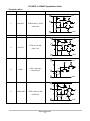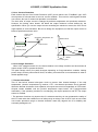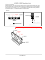
1
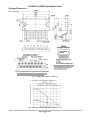
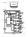
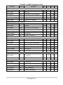
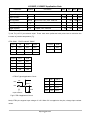
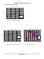
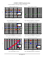
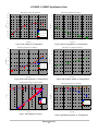
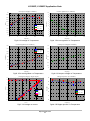
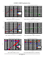
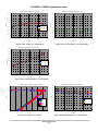
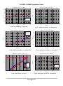
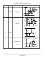
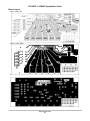
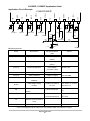
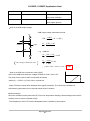
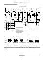
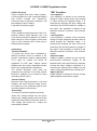
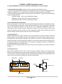
LV5692P, LV5693P Multi Voltage Regulator IC Application Note Overview LV5692P/93P is a multiple voltage regulator for car audio system, which allows reduction of quiescent current. This IC has 5 systems of voltage regulator, pre-driver for Pch- FET which generates USB power and a high side switch for external devices. The following protection circuits are integrated: overcurrent protector, overvoltage protector and Thermal Shut Down. This IC is suitable for use in car audio with USB port. The package is HZIP15J Functions Quiescent Current 50uA ( Typ, when only VDD is in operation) 5 channel regulators and 1channel P-FET pre-driver (for USB-POWER) ・ For VDD: Vout is 3.3V(LV5692P),5.7V(LV5693P), Iomax is 300mA ・ For DSP: Vout is 3.3V, Iomax is 300mA ・ For CD: Vout is 8.0V, Iomax is 1300mA ・ For Ilumi: Vout is 8.4V, Iomax is 500mA ・ For Audio:Vout is 8.4V, Iomax is 500mA ・ For USB (Controller) , Vout is flexible (configurable with external resistor) , Iomax is 1000mA High-side switch :Voltage difference between input and output is 0.5V, Iomax is 500mA Overcurrent protector Overvoltage protector Thermal Shut Down (Without VDD-OUT) *Detection voltage is 21V (typical) *175ºC (typical) (Warning) The protector functions only improve the IC’s tolerance and they do not guarantee the safety of the IC if used under the conditions out of safety range or ratings. Use of the IC such as use under over-current protection range or thermal shutdown state may degrade the IC’s reliability and eventually damage the IC. LV5692P, LV5693P Application Note Package Dimensions unit : mm(typical) Fig1. Package Dimensions of HZIP15J Fig2. Allowable Power Dissipation Derating Curve http://onsemi.com 2 LV5692P, LV5693P Application Note Pin Assignment LV5692/93 15pin ILM GND CD CTRL1 M AUDIO D CTRL2 D DSP 1 CTRL3 O FB 2 USBGT P EXT 3RSNS B VDD T VCC1 T VCC S D 1 C 1pin Fig3. Pin Assignment Block Diagram Vcc AMP out Over Voltage Protection EXT_HS-SW(VCC-1 V) Start 500mA up - Vref + ILM(8.4V) 500mA AUDIO(8.4V) + 500mA CTRL1 Vcc OUTPUT CTRL2 Ilim - Control FET:2SJ650 + CTRL3 USB(5V) 1000mA + Thermal Shut Down CD(8V) 1300mA Vcc1 + GND Vcc VDD(3.3V: LV5692P) VDD(5.7V: LV5693P) 300mA + DSP(3.3V) 300mA Fig4. Block Diagram http://onsemi.com 3 LV5692P, LV5693P Application Note Specifications Absolute Maximum Ratings at Ta=25 ºC Parameter Power supply voltage Power dissipation Symbol Vcc max Pd max (*1) ・IC Unit Operating temperature Topr Storage temperature Tstg Ratings Unit 36 V 1.5 ・At using Al heat sink of “50×50×1.5mm 3 5.6 ・At Infinite heat sink W 32.5 Vcc peak ・Regarding waveform, refer to below Peak voltage * Conditions 50 V -40 to +85 ºC -55 to ºC +150 1: Ta≤25ºC ・Peak Voltage testing pulse wave 50V 90% 10% 16V 5msec 100msec Fig5. Peak Voltage testing pulse wave Recommended Operating Ranges at Ta=25ºC Parameter Conditions Power supply voltage rating 1 VDD-OUT ON, DSP-OUT ON Power supply voltage rating 2 ILM-OUT ON Power supply voltage rating 3 AUDIO-OUT ON, CD-OUT ON *VCC1 should be as follows: VCC1>VCC-0.7V http://onsemi.com 4 Rating Units LV5692P: 7 to 16 LV5693P: 7.7 to 16 V 10.8 to 16 V 10 to 16 V LV5692P, LV5693P Application Note Electrical Characteristics Vcc=Vcc1=14.4V at Ta=25ºC (*2) Parameter Quiescent Current Symbol Icc Conditions Min Typ 50 VDD: No Load,CTRL1/2/3=”L/L/L” Max Units 100 μA 0.3 V 2.10 V 5.50 V 520 kΩ 0.3 V CTRL1 Input Voltage Level “L” Input voltage VIL1 0 “M” Input voltage VIM1 1.10 “H” Input voltage VIH1 2.50 Input impedance RIN1 280 1.65 400 CTRL2 Input Voltage Level “L” Input voltage VIL2 “M1” Input voltage VIM12 0.8 1.06 1.4 V “M2” Input voltage VIM22 1.90 2.13 2.40 V “H” Input voltage VIH2 2.9 3.2 5.5 V Input impedance RIN2 280 400 520 kΩ 0 CTL3 Input Voltage Level “L”Input voltage VIL3 0 0.3 V “H” Input voltage VIH3 2.5 5.5 V Input impedance RIN3 280 400 520 kΩ 3.3 3.45 V VDD 3.3V OUT (LV5692P) Output Voltage Vo1 Io1= 200 mA, 3.16 Output Current Io1 Vo1≥3.1V 300 Line regulation ∆VoLN1 7.5V<Vcc1<16 V, Io1= 200 mA 30 100 mV Load regulation ∆VoLD1 1 mA<Io1<200 mA 70 150 mV Ripple rejection RREJ1 f=120Hz, Io1= 200 mA 30 mA 40 dB 5.7 5.985 V VDD 5.7V OUT (LV5693P) Output Voltage Vo1 Io1= 200 mA, Output Current Io1 Vo1≥5.35V Line regulation ∆VoLN1 8.2V<Vcc1<16 V, Io1= 200 mA 30 100 mV Load regulation ∆VoLD1 1 mA<Io1<200 mA 70 150 mV Dropout voltage1 VDROP1 Io1= 200 mA 0.5 1.2 V Dropout voltage 2 VDROP1’ Io1= 100 mA 0.25 0.6 V Ripple rejection RREJ1 f=120Hz, Io1= 200 mA http://onsemi.com 5 5.415 300 30 mA 40 dB LV5692P, LV5693P Application Note Parameter USB ; CTRL3=“H” Symbol Conditions (External Pch-FET Min Typ Max Units (2SJ650) , Resistors: 27kΩ, 9.1kΩ) Output Voltage Vo2 Io2= 1000 mA 4.75 Output Current Io2 Vo2≥4.75V 1000 Line regulation ∆VoLN2 10 V<Vcc<16 V, Io2= 1000 mA Load regulation ∆VoLD2 10 mA<Io2<1000 mA Dropout voltage VDROP2 Io2= 1000 mA Ripple rejection RREJ2 f=120Hz ,Io2= 1000 mA 5 5.25 V mA 50 90 mV 100 150 mV 1 1.5 V 40 50 8.4 dB AUDIO (8.4V) OUT; CTRL1= ”M or H” Output Voltage Vo3 Io3= 400 mA 8.0 8.8 V Output Current Io3 Vo3≥8.0V 500 Line regulation ∆VoLN3 10V<Vcc<16 V, Io3= 400 mA 30 90 mV Load regulation ∆VoLD3 1 mA<Io3<400 mA 70 150 mV Dropout voltage1 VDROP3 Io3= 400 mA 0.4 0.8 V Dropout voltage2 VDROP3’ Io3= 200 mA 0.2 0.4 V Ripple rejection RREJ3 f=120Hz, Io3=400 mA mA 40 50 8.0 8.4 dB ILM (8.4V) OUT; CTRL2= ”M1 or H” Output Voltage Vo4 Io4= 400 mA 8.8 Output Current Io4 Line regulation ∆VoLN4 10.8V<Vcc<16 V, Io4= 400 mA 30 90 mV Load regulation ∆VoLD4 1 mA<Io4<400 mA 70 150 mV Dropout voltage1 VDROP4 Io4= 400 mA 1.0 1.5 V Dropout voltage2 VDROP4’ Io4= 200 mA 0.7 1.05 V Ripple rejection RREJ4 f=120Hz, Io4= 400 mA 500 40 V mA 50 dB EXT_HS-SW; CTRL2= “M2 or H” Output Voltage Vo5 Io5= 500 mA Output Current Io5 Vo5≤Vcc-1V Vcc Vcc -0.5 -1.0 500 V mA DSP (3.3V) OUT; CTRL1= “M or H” Output Voltage Vo7 Io7= 200 mA 3.1 3.3 3.5 Output Current Io7 Line regulation ∆VoLN7 10V<Vcc<16 V, Io7= 200 mA 30 90 mV Load regulation ∆VoLD7 1 mA<Io4<200 mA 70 150 mV Ripple rejection RREJ7 f=120Hz, Io4= 200 mA 300 http://onsemi.com 6 40 V mA 50 dB LV5692P, LV5693P Application Note Parameter Symbol Conditions Min Typ Max Units CD (8.0V) OUT; CTRL1=“H” Output Voltage Vo8 Io8= 1000 mA 7.6 Output Current Io8 Line regulation ∆VoLN8 10.5V<Vcc<16 V, Io8= 1000 mA Load regulation ∆VoLD8 Dropout voltage Ripple rejection 8.0 8.4 1300 V mA 50 100 mV 10 mA<Io8<1000 mA 100 200 mV VDROP8 Io8= 1000 mA 1.0 1.5 V RREJ8 f=120Hz ,Io8= 1000 mA 40 50 dB *2: The entire specification has been defined based on the tests performed under the conditions where Tj and Ta (=25 ºC) are almost equal. These tests were performed with pulse load to minimize the increase of junction temperature (Tj). CTRL PINS TRUTH-VALUE TABLE CTRL1 CD DSP Audio CTRL3 USB L OFF OFF OFF L OFF M OFF ON ON H ON H ON ON ON CTRL2 EXT ILM L OFF OFF M1 OFF ON M2 ON OFF H ON ON ・CTRL2 Typical Application Circuit EXT 24k CTRL2 ILM 47k 400k EXT ILM CTRL2 0V 0V 0V 0V 3.3V 1.06V 3.3V 0V 2.13V 3.3V 3.3V 3.20V Input resistors Fig6. CTRL2 Application Circuit Note) CTRL pins support input voltage of 3.3V. When 5V is supplied to the pins, change input resistor values. http://onsemi.com 7 LV5692P, LV5693P Application Note (Warning) Usage of CTRL2 When CTRL pin transits between L and M2, since it passes M1, ILM is turned on for a moment. Likewise, when CTRL pin transits between H and M1, since it passes M2, ILM is turned off for a moment. To avoid operation failure by the above factors, please refer to the following precautions. * Do not connect parasitic capacitor to CTRL as much as possible. * If use of capacitor for CTRL is required, keep the resistance value as low as possible. * Make sure that the output load capacitor has enough margin against the voltage fluctuation due to instantaneous ON/OFF. http://onsemi.com 8 LV5692P, LV5693P Application Note Timing Chart 21V VCC (15PIN) 21V 6.2V VCC1 (14PIN) VDD-OUT H (13PIN) M CTRL1(Input) (4PIN) L H M2 CTRL2(Input) (6PIN) M1 L CTRL3(Input) (8PIN) AUDIO-OUT (5PIN) DSP-OUT (7PIN) CD-OUT I (3PIN) L ILM-OUT (1PIN) M EXT-OUT (11PIN) USB-GT (FET-OUT) Fig7. Timing Chart http://onsemi.com 9 LV5692P, LV5693P Application Note Typical Characteristics(LV5693P) Quiescent current 80 70 Istby (uA) 60 50 40 VCC=7V VCC=14.4V VCC=16V 30 20 -50 0 50 temp(deg.) 100 150 Fig8. Quiescent current vs Temperature 16 0.7 14 0.6 12 0.5 10 0.4 VCC=7.5V VCC=14.4V VCC=16V 0.3 Vo (V) Vo (V) EXT output drop voltage (Io=500mA) 0.8 EXT output voltage vs output current 8 -40℃ 25℃ 85℃ 125℃ Iomax 6 0.2 4 0.1 2 0 0 -50 0 50 100 150 0 temp(deg.) 0.2 0.4 0.6 0.8 1 Io (A) Fig9. EXT drop voltage vs Temperature http://onsemi.com 10 Fig10. EXT voltage vs current 1.2 1.4 1.6 LV5692P, LV5693P Application Note In case of LV5692P, VDD output voltage is 3.3V typical. VDD output voltage(Io=200mA) 5.8 VDD line regulation (Io=200mA) 40 38 36 5.75 5.7 Vline (mV) Vo (V) 34 VCC=8.2V VCC=14.4V 32 30 28 26 VCC=16V 5.65 24 22 20 5.6 -50 0 50 100 -50 150 0 Fig11. VDD voltage vs Temperature 100 150 Fig12. VDD Line regulation vs Temperature VDD load regulation (Io=200mA) 30 50 temp(deg.) temp(deg.) VDD dropout voltage (Io=200mA) 0.8 VCC=8.2V 0.7 VCC=14.4V 20 VCC=16V 0.6 0.5 Vdrop (V) Vload (mV) 10 0 -10 0.4 0.3 0.2 -20 0.1 0 -30 -50 0 50 100 -50 150 0 temp(deg.) Fig13. VDD Load regulation vs Temperature 100 150 Fig14. VDD dropout voltage vs Temperature VDD output voltage vs output current 7 50 temp(deg.) VDD ripple rejection (Io=200mA) 60 6 55 5 Rrej (dB) Vo (V) 50 4 -40℃ 25℃ 85℃ 125℃ Iomax 3 2 45 40 VCC=8.2V VCC=14.4V 35 1 0 VCC=16V 30 0 0.1 0.2 0.3 0.4 0.5 0.6 0.7 -50 Io (A) Fig15. VDD voltage vs current 0 50 100 temp(deg.) Fig16. VDD Ripple rejection vs Temperature http://onsemi.com 11 150 LV5692P, LV5693P Application Note ILM line regulation(Io=400mA) ILM output voltage (Io=400mA) 8.48 4.5 8.46 4 8.44 3.5 8.42 3 Vline (mV) 5 Vo (V) 8.5 8.4 8.38 2.5 2 8.36 VCC=10.8V 1.5 8.34 VCC=14.4V 1 8.32 VCC=16V 0.5 0 8.3 -50 0 50 100 -50 150 0 50 100 150 temp(deg.) temp(deg.) Fig17. ILM voltage vs Temperature Fig18. ILM Line regulation vs Temperature ILM load regulation (Io=400mA) ILM dropout voltage(Io=400mA) 60 1.4 50 1.2 1 30 VCC=10.8V Vdrop (V) Vload (mV) 40 0.8 0.6 VCC=14.4V 20 0.4 VCC=16V 10 0.2 0 0 -50 0 50 100 -50 150 0 100 150 temp(deg.) temp(deg.) Fig19. ILM Load regulation vs Temperature Fig20. ILM dropout voltage vs Temperature ILM output voltage vs output current 10 50 ILM ripple rejection (Io=400mA) 80 9 75 8 70 7 65 Rrej (dB) Vo (V) 6 5 -40℃ 25℃ 85℃ 125℃ Iomax 4 3 2 60 55 VCC=10.8V VCC=14.4V 50 VCC=16V 45 1 0 40 0 0.2 0.4 0.6 0.8 1 1.2 -50 0 Io (A) Fig21. ILM voltage vs current 50 100 temp(deg.) Fig22. ILM Ripple rejection vs Temperature http://onsemi.com 12 150 LV5692P, LV5693P Application Note CD line regulation (Io=1000mA) CD otuput voltage(Io=1000mA) 8.08 9 8.06 8 8.04 7 8.02 6 8 VCC=10V 7.98 VCC=14.4V 7.96 Vline (mV) 10 Vo (V) 8.1 5 4 3 VCC=16V 7.94 2 7.92 1 0 7.9 -50 0 50 100 -50 150 0 100 150 temp(deg.) temp(deg.) Fig23. CD voltage vs Temperature Fig24. CD Line regulation vs Temperature CD load regulation (Io=1000mA) 160 CD dropout voltage(Io=1000mA) 1.6 140 1.4 VCC=10V VCC=14.4V VCC=16V 120 1.2 100 1 Vdrop (V) Vload (mV) 50 80 60 0.8 0.6 40 0.4 20 0.2 0 0 -50 0 50 100 150 -50 0 temp(deg.) Fig25. CD Load regulation vs Temperature 100 150 Fig26. CD dropout voltage vs Temperature CD output voltage vs output current 9 50 temp(deg.) CD ripple rejection (Io=1000mA) 70 8 65 7 60 Rrej (dB) Vo (V) 6 5 4 -40℃ 25℃ 85℃ 125℃ Iomax 3 2 55 VCC=10V VCC=14.4V 50 VCC=16V 45 1 40 0 0 0.5 1 1.5 2 2.5 -50 50 100 temp(deg.) Io (A) Fig27. CD voltage vs current 0 Fig28. CD Ripple rejection vs Temperature http://onsemi.com 13 150 LV5692P, LV5693P Application Note AUDIO line regulation (Io=400mA) AUDIO output voltage(Io=400mA) 8.48 4 8.46 3 8.44 2 8.42 1 Vline (mV) 5 Vo (V) 8.5 8.4 8.38 VCC=10V 8.36 VCC=14.4V -1 -2 VCC=16V 8.34 0 -3 -4 8.32 -5 8.3 -50 0 50 100 -50 150 0 50 100 150 temp(deg.) temp(deg.) Fig29. AUDIO voltage vs Temperature Fig30. AUDIO Line regulation vs Temperature AUDIO load regulation (Io=400mA) AUDIO dropout voltage(Io=400mA) 60 1 0.9 50 0.8 0.7 Vdrop (V) Vload (mV) 40 30 20 10 0.6 0.5 0.4 VCC=10V 0.3 VCC=14.4V 0.2 VCC=16V 0.1 0 0 -50 0 50 100 -50 150 0 100 150 temp(deg.) temp(deg.) Fig31. AUDIO Load regulation vs Temperature Fig32. AUDIO dropout voltage vs Temperature AUDIO output voltage vs output current 10 50 AUDIO ripple rejection(Io=400mA) 80 9 75 8 70 7 65 Rrej(dB) Vo (V) 6 5 -40℃ 25℃ 85℃ 125℃ Iomax 4 3 2 60 55 VCC=10V VCC=14.4V VCC=16V 50 45 1 40 0 0 0.2 0.4 0.6 0.8 1 1.2 -50 50 100 temp(deg.) Io (A) Fig33. AUDIO voltage vs current 0 Fig34. AUDIO Ripple rejection vs Temperature http://onsemi.com 14 150 LV5692P, LV5693P Application Note DSP output voltage(Io=200mA) DSP line regulation (Io=200mA) 3.38 1.8 3.36 1.6 3.34 1.4 3.32 1.2 3.3 Vline (mV) 2 Vo (V) 3.4 VCC=10V VCC=14.4V VCC=16V 3.28 3.26 1 0.8 0.6 3.24 0.4 3.22 0.2 3.2 0 -50 0 50 100 150 -50 0 temp(deg.) 50 100 150 temp(deg.) Fig35. DSP voltage vs Temperature Fig36. DSP Line regulation vs Temperature DSP load regulation (Io=200mA) 20 18 16 Vload (mV) 14 12 VCC=10V 10 VCC=14.4V 8 VCC=16V 6 4 2 0 -50 0 50 100 150 temp(deg.) Fig37. DSP Load regulation vs Temperature DSP output voltage vs output current 4 DSP ripple rejection (Io=200mA) 80 78 3.5 76 3 74 Rrej(dB) Vo (V) 2.5 2 -40℃ 25℃ 85℃ 125℃ Iomax 1.5 1 72 70 VCC=10V 68 VCC=14.4V 66 VCC=16V 64 0.5 62 60 0 0 0.1 0.2 0.3 0.4 0.5 0.6 0.7 -50 50 100 temp(deg.) Io (A) Fig38. DSP voltage vs current 0 Fig39. DSP Ripple rejection vs Temperature http://onsemi.com 15 150 LV5692P, LV5693P Application Note USB line regulation (Io=1000mA) USB output voltage(Io=1000mA) 5.1 2 5.06 1.6 5.04 1.4 5.02 1.2 5 4.98 VCC=10V VCC=14.4V VCC=16V 4.96 4.94 Vline (mV) 1.8 Vo (V) 5.08 1 0.8 0.6 0.4 0.2 4.92 0 4.9 -50 0 50 100 -50 150 0 Fig40. USB voltage vs Temperature 150 USB dropout voltage(Io=1000mA) 0.5 VCC=10V VCC=14.4V VCC=16V 25 0.45 0.4 0.35 Vdrop (V) 20 Vload (mV) 100 Fig41. USB Line regulation vs Temperature USB load regulation (Io=1000mA) 30 50 temp(deg.) temp(deg.) 15 10 0.3 0.25 0.2 0.15 0.1 5 0.05 0 0 -50 0 50 100 150 -50 0 temp(deg.) Fig42. USB Load regulation vs Temperature 100 150 Fig43. USB dropout voltage vs Temperature USB output voltage vs output current 6 50 temp(deg.) USB ripple rejection (Io=1000mA) 60 58 5 56 54 Rrej(dB) Vo (V) 4 3 -40℃ 25℃ 85℃ 125℃ Iomax 2 52 50 48 VCC=10V VCC=14.4V VCC=16V 46 44 1 42 40 0 0 0.5 1 1.5 2 2.5 3 3.5 -50 50 100 temp(deg.) Io (A) Fig44. USB voltage vs current 0 Fig45. USB Ripple rejection vs Temperature http://onsemi.com 16 150 LV5692P, LV5693P Application Note Terminal outline Pin No Name Function Equivalent circuit VCC 15 1 1 ILM-OUT 256kΩ CTRL2=M1,H ON 8.4V/0.5A 45kΩ 1kΩ GND 2 2 GND GND VCC 15 3 3 CD-OUT CTRL1=H ON 241kΩ 8.0V/1.3A 45kΩ 1kΩ GND 2 15 4 CTRL1 CTRL1 Input pin 3 value-input VCC 10kΩ 4 400kΩ 2 GND 15 VCC 5 256kΩ 5 AUDIO-OUT CTRL1=M,H ON 8.4V/0.5A 45kΩ 2 http://onsemi.com 17 1kΩ GND LV5692P, LV5693P Application Note Pin No Name Function Equivalent circuit 15 6 CTRL2 VCC CTRL2 Input pin 4 value-input 6 400kΩ 2 15 VCC 7 73kΩ 7 DSP-OUT CTRL1=M,H ON 3.3V/0.3A 45kΩ 8 CTRL3 2 GND 15 VCC CTRL3 Input pin 2 value-input 1kΩ 10kΩ 8 400kΩ 2 GND 15 VCC USB Feedback pin 9 1kΩ FB 1kΩ 1.26V 9 1kΩ 2 http://onsemi.com 18 GND LV5692P, LV5693P Application Note Pin No Name Function Equivalent circuit 15 VCC 10 10 USBGT 1kΩ Pch-FET gate drive 12.0V GND 2 15 11 EXT VCC CTRL2=M2,H ON 11 VCC-0.5V/500mA 2 GND VCC 15 USB current detection 12 RSNS 12 5kΩ 5kΩ resistor connect pin 14.3V VDD-OUT GND 14 VCC1 13 VDD (Micon) 13 2 R 3.3V/0.3A:LV5692P 5.7V/0.3A:LV5693P 140kΩ 1kΩ GND 2 R=435kΩ(LV5693P) R=240 kΩ(LV5692P) 14 VCC1 Vin for VDD 15 VCC Vin (B+) VCC 15 2 http://onsemi.com 19 14 VCC1 GND LV5692P, LV5693P Application Note Board Layout ・Layer 1(Top) silk ・Layer 1(Top) metal Fig53. Top Layer ・Layer 2(Bottom) metal Fig54. Bottom Layer http://onsemi.com 20 LV5692P, LV5693P Application Note Application Circuit Example + C2 + C4 C1 ILM-OUT CD-OUT C6 C8 AUDIO-OUT CTRL1 D3 C18 C16 C17 C15 VDD-OUT C12 C13 CTRL3 VCC 15 + + D2 DSP-OUT 14 13 + C7 VCC1 RSNS 12 11 C14 CTRL2 VDD 10 9 + C5 EXT USBGT 8 7 + C3 CTRL3 CTRL2 6 5 FB 4 3 DSP 2 1 AUDIO CD ILM GND CTRL1 LV5692P/5693P + C20 C19 D1 M1 EXT-OUT R2 R1 R3 2SJ650/2SJ54 0 C11 + C10 USB VCC ■External parts list Part # Descriptions Recommendation Others value C2,C4,C6,C8,C11,C16 Output voltage stabilizer 10uF or higher E-cap (Note1) C1,C3,C5,C7,C10,C15 Output voltage stabilizer 0.22uF or higher Ceramic-cap (Note1) C12,C13 Phase compensator C12=1000pF, Ceramic-cap (C13=0pF: TBD) C18,C20 By-pass 100μF or higher Connect them close to C17,C19 OSC preventers 0.22μF or higher VCC and GND C14 EXT output voltage 2.2μF or higher stabilizer USB voltage setting R1/R2=9.1kΩ/27kΩ resistor for 5.0V R1,R2 USB current limit setting R3 M1 resistor 0.1Ω for Ipeak=3A better than ±1% Panasonic ERJB1CFR10U (ref) USB-OUT Pch-FET 2SJ650 (to be discontinued) D1 Use resistor w/ accuracy Renesas 2SJ540 SFT1342 Reverse Current prevention diode D2,D3 IC crash preventer diode SB1003M3 *The circuit diagram and the values are only tentative which are subject to change. http://onsemi.com 21 LV5692P, LV5693P Application Note (Note1) Make sure that the capacitors of the output pins are 10uF or higher and ESR is 10ohm or lower in total and temperature characteristics and accuracy are taken into consideration. Also the E-cap should have good high frequency characteristics. How to set USB application ■USB block diagram R3 RSNS LIM M1 Vref USB USBGT C12 R2 FB C10 C11 R1 ■General description USB output is controled by CTRL3 pin. USBGT(PIN10) is gate drive terminal of P-channel FET. FB(PIN9) is feedback input. RSNS(PIN12) is current sense input. When voltage difference (VCC-RSNS) exceeds 0.3V, current limits output current and foldback output voltage. Limit current is determined by following equation. Io_lim(A)=0.3V/R3(ohm) ■Example parts list R1/R2=9.1kΩ/27kΩ R1,R2 USB voltage setting resistor R3 USB current limit setting resistor C10 Output voltage stabilizer for 5.0V 0.1Ω for Ipeak=3A 0.22uF or higher Use resistor w/ accuracy better than ±1% Panasonic ERJB1CFR10U (ref) Ceramic-cap (Note1) C11 Output voltage stabilizer 10uF or higher E-cap (Note1) C12,C13 Phase compensator C12=1000pF, Ceramic-cap C13=0pF *The purpose of C12 is phase compensation of negative feedback, which guarantees regulator stability. Recommended value range of C12 is between 470p~2000pF. If you use the value out of the range, it causes the effect described below. http://onsemi.com 22 LV5692P, LV5693P Application Note C12 advantage smaller value disadvantage rapid response lack of stability may cause oscillation greater value stability increase slow transient response worse ripple rejection ・How to set USB output voltage: USB output voltage calculation formula. VC C USB R 12 3 10 USBGT USB 1.26[V ] R2 1.26[V ] R1 R2 USB 1.26 R1 1.26 R FB 1.26V 9 2 R1 FB -voltage is defined by Vref e.g. USB=5V R2 5.0 1.26 2.968 R1 1.26 R2 27k 2.967 R1 9.1k * USB 1.26V 2.967 1.26V 4.998V ・How to set USB over-current limit value (OCP) OCP of the USB works when the voltage of RSNS is under “VCC-0.3V”. The peak current value of OCP is calculated as follows: “Ipeak (A) =0.3/R3” e.g. R3=0.1ohm Ipeak=3A Ipeak (Note) The above values were obtained under typical conditions. The values have tolerance in manufacturing processes due to external resistor and IC variation. ■Thermal design Since the controller cannot protect the FET from over-temperature damage, thermal design care must be carefully done to assure a reliable design. The temperature of the FET and the dissipated power is defined by the equation. http://onsemi.com 23 LV5692P, LV5693P Application Note ■PCB layout consideration For maximum accuracy, VCC and RSNS pins must be Kelvin connected to R3, to avoid errors caused by voltage drops along the traces carrying the current from the VCC to the Source pin of the FET. ■Warning The internal circuits of USBGT and RSNS consist of components that support 5V. Do not bias 7V or above between VCC and these pins to prevent the IC from destruction. Do not use the device under over-voltaged condition(for example shorting these terminals to low voltage node) even for short period of time . In normal operating condition with recommended application, the device controls voltage of these terminals within 5V. ■Application information using other FET You can replace 2SJ650 with 2SJ540 or SFT1342 .(2SJ650 is to be discontinued.) In case of using 2SJ540/SFT1342, value of all resisters and capacitors will be the same as the case of using 2SJ650. Since SFT1342's package is different from that of 2SJ650/2SJ540, thermal design care must be carefully done to assure a reliable design. You must use the FET under the condition so that the power dissipation of FET does not exceed allowable power dissipation. http://onsemi.com 24 LV5692P, LV5693P Application Note Demonstration-board schematics VCC1 RSNS 12 11 VCC 10 9 VDD 8 7 EXT USBGT CTRL3 CTRL2 6 5 FB 4 3 DSP 2 1 AUDIO CTRL1 CD GND ILM LV5692P/5693P 14 13 15 C18 C17 C14 C2 C1 C4 C3 ILM C6 CD C5 C8 AUDIO CTRL2 CTRL1 +3.3V C7 D2 DSP D3 R1 R11 47k AUDIO /DSP C20 C19 VDD C12 C13 CTRL3 47k C16 C15 9.1k D1 27k EXT M1 R2 R3 2SJ540 0.1 R12 +CD R13 24k ILM ■demo board parts constants C1,C3,C5,C7,C10,C15,C17,C19=0.22uF C2,C4,C6,C8,C11,C16=10uF Fig46. C13: 0p C12=1000pF、C14=2.2uF C18,C20=100uF R3:Panasonic ERJB1CFR10U M1: Renesas 2SJ540 ・all ceramic capacitors are chip condensers. ・The parts indicated by dotted line are not mounted. 47k R15 USB VCC1 C10 R14 EXT USB C11 47k VCC demo-board schematics ■Jumper connector setting OFF ON OFF ON OFF ON +CD USB EXT ILM AUDIO /DSP state: OFF AUDIO/DSP=ON AUDIO/DSP/CD=ON OFF ON state: each-ch OFF OFF ON each-ch ON ・"USB" output current is from external FET. This channel has over-current limiter, but you should be careful of over heat of FET. You should consider power dissipation of FET when you determine the limit current or heat sink specification. Limit current (peak current(A)) is calculated by 0.3/R3. http://onsemi.com 25 LV5692P, LV5693P Application Note Bill of Materials Reference Value Part Vendor Comments C18,20 100μF/50V UVR1H101MPD nichicon Capacitor, Aluminum Electrolytic C1,3,5,7,10 C15,17,19 0.22μF/50V GRM21BR71H224KA01L Murata Capacitor, Ceramic C12 1000pF/50V GRM188R71H102KA01D Murata Capacitor, Ceramic C14 2.2μF/50V UVK1H2R2MDD nichicon Capacitor, Aluminum Electrolytic C2,4,6 C8,11,16 10μF/25V UMA1E100MDD/ ECEA1FKS100 nichicon/ Panasonic Capacitor, Aluminum Electrolytic R1 9.1kΩ/±1% MF1/4CCT52A9101F KOA Resistor R2 27kΩ/±1% MF1/4CCT52A2702F KOA Resistor R3 0.1Ω/1W ERJB1CFR10U Panasonic Resistor, Thick Film R11,12,13, R15 47kΩ MFS1/4CCT52A4702F KOA Resistor R14 24kΩ MFS1/4CCT52A2402F KOA Resistor 2SJ540-E Renesas P-ch power FET W81136T3843RC RS Board Header SL* W8010T50RC RS Short Link TP ST-4-2 MAC8 Test Point M1 BH(3pins) 3pins http://onsemi.com 26 LV5692P, LV5693P Application Note Functional Description The LV5693P is a multiple output voltage regulator with a power switch, suitable for use in car audio system. [Standby mode] When all CTRL pins are "L" state (CTRL1=CTRL2=CTRL3=L), LV5692P/93P is in standby mode. In standby mode, all outputs except VDD are disabled. Quiescent current is 50uA(typ) at VDD no load. When either CTRL pin exceeds "M1" threshold voltage, LV5693P exits standby mode. [VCC] This IC has the tolerance value of 50V against VCC peak surge voltage, but for more safety set design, adding power clamp, such as power zenner diode, on battery connected line is recommended in order to absorb applied surge. This IC has no protection against battery reverse connection, so adding Schottky diode is recommended to prevent a negative voltage. [Linear Regulators] All regulators in LV5692P/93P are low dropout outputs, because the output stage of all regulators is Pch-LDMOS. When you select output capacitors for linear regulators, you should consider three main characteristics: startup delay, transient response and loop stability. The capacitor values and type should be based on cost, availability, size and temperature constraints. Tantalum, Aluminum electrolytic, Film, or Ceramic capacitors are all acceptable solutions. However, attention must be paid to ESR constraints. The aluminum electrolytic capacitor is the least expensive solution, but if the circuit operates at low temperatures(-25 to -40 ℃ ), both the value and ESR of the capacitor will vary considerably. The capacitor manufacturer's datasheet usually provides this information. VDD5V regulator (3.3V, 0.3A:LV5692P) (5.7V, 0.3A:LV5693P) When VCC is applied, VDD output is active regardless of CTRL states. The charge on VCC1 capacitor can be used to supply VDD output for a short period when VCC voltage drops 0V. CD regulator (8.0V, 1.3A) AUDIO regulator (8.4V, 0.5A) ILM regulator (8.4V, 0.5A) DSP regulator (3.3V, 0.3A) These regulators are controled by CTRL1/2 pins. Logic table is shown on page7. USB regulator (5V, 1.0A) USB output is controled by CTRL3 pin. USBGT(PIN10) is gate drive terminal of P-channel FET. FB(PIN9) is feedback input. RSNS(PIN12) is current sense input. When voltage difference (VCC-RSNS) exceeds 0.3V, current limits output current and foldback output voltage.Limit current is determined by following equation. Io_lim(A)=0.3V/R3(ohm) For maximum accuracy, VCC and RSNS pins must be Kelvin connected to R3, to aviod errors caused by voltage drops along the traces carrying the current from the VCC to the Source pin of the FET. For more information about USB application, refer to "How to set USB application" on page22. [EXT high-side switches] These are high-side power switches connected to VCC. If these output are connected to inductive load or loads which have different ground potential, protection diodes (D2/D3) are necessary to protect the device from negative voltage. [over current protection] When the each output becomes in over load conditon, the device limits the output current.All outputs are also protected against short circuit by fold back current limitter. http://onsemi.com 27 LV5692P, LV5693P Application Note [CTRL1/2/3 input] CTRL1 accepts three input values (L/M/H)., CTRL2 accepts four input values(L/M1/M2/H) and CTRL3 accepts two values(L/H). CTRL1/2/3 have a pull-down resistance, and this resistance value is 400kΩ. Logic table is shown on page7. [VCC/VCC1] VCC1 voltage must be higher than VCC-0.7V, because internal diode between VCC and VCC1 becomes positively biased. This internal diode cannot be used to supply current from VCC to VCC1 because this is used only for ESD protection purpose. [Protection] Thermal Shutdown To protect the device from overheating a thermal shutdown circuit is included. If the junction temperature reaches approximately 175 ℃ (typ), all outputs are turned off regardless of CTRL state. Outputs remain disabled until the junction temperature drops below 145℃(typ)(automatic restoration). The thermal shutdown circuit does not guarantee the protection of the final product because it operates out of maximum rating (exceeding Tjmax=150℃). Current Limiting When the each output becomes in over load condition, the device limits the output current. All outputs are also protected against short circuit by fold back current limiter. Overvoltage The device is protected against load dump. When VCC voltage exceeds 21V, the device detects over voltage condition and turns all the outputs off except VDD to protect the device. If VCC voltage gets below 21V, outputs are automatically restored. TEST Procedure Line regulation Line regulation is defined as the maximum change in output voltage as the input voltage is varied through the specified range. It is measured by changing the input voltage and measuring the minimum/maximum voltage of the output. Line regulation is defined as the difference between maximum and minimum voltage. Load regulation Load regulation is defined as the maximum change in output voltage as the load current is varied through the specified range. It is measured by changing the load current and measuring the minimum/maximum voltage of the output. Load regulation is defined as the difference between maximum and minimum voltage. Dropout voltage Dropout voltage is defined as the minimum input-to-output differential voltage at the specified load current required by the regulator to keep the output voltage in regulation. It is measured by reducing input voltage until the output voltage drops below the nominal value. Ripple rejection Ripple rejection is defined as the ratio of input ripple amplitude versus that of output. http://onsemi.com 28 LV5692P, LV5693P Application Note In using LV5692P/93P, you have to check the following prior to the set design. 1. Absolute Maximum Rating (Common notes to general semiconductor device) Stresses exceeding Maximum Ratings may damage the device. If stresses exceeding Maximum Ratings are applied to an IC, it might smoke or fire by the breakdown and the overheating. We recommend derating design for reducing failure rate of device. A guide of general derating design is described below. (1)Stress Voltage: 80% or less for Abs Max voltage. (2)Maximum rating current: 80% or less for Abs Max Io. (3)Temperature: 80% or less for Temperatures rating. 2. Recommended Operating Range When Power Supply IC was used in Recommended Operating Rating and Temperature rating, IC’s characteristics are guaranteed. Unless otherwise specified, we do not guarantee the specified value in all temperature ranges. As long as the IC is at operation temperature range, IC’s characteristic doesn’t change suddenly. Operating conditions of the input voltage and the output current are limited by the chip maximum junction temperature (Tjmax). Please decide the value of the input voltage and the output current so as not to exceed Tjmax. 3. Output Capacitor Between GND and each output, please be sure to put capacitor to prevent oscillation. Because abrupt changes of input voltage and output load interfere in the output voltage, make sure to use the system that will actually be offered to the market and define the output capacitor after a sufficient evaluation. When selecting the capacitor, to ensure the required minimum capacity over all operating conditions of the application, it is necessary to consider the influence of temperature and applied voltage on the capacity value. Please design the PCB layout that the output terminal and the capacitor are located as close as possible. 4. Parasitic Devices Output Power MOS-FET driver has, in device structure, parasitic diode like the figure below. Because in normal operating the input voltage is higher than the output voltage, the parasitic diode is reverse bias. If the output is higher than the input at abnormal operating, a current flows from the output to the input, because the parasitic diode is forward biased. SOURCE(S) GATE(G) SOURCE(S) p+ p+ n n GATE(G) Parasitic diode p- Parasitic diode p+ DRAIN(D) DRAIN(D) http://onsemi.com 29 LV5692P, LV5693P Application Note 5. Over -Current Protection Each channel has an Over-Current Protection (OCP) circuit which is the "Fold-Back" type, OCP circuit prevent IC’s break down at an over current condition. This circuit is useful against sudden over current, but use of continuous operation is not allowed. The limit value of output current is changed by ambient temperature and production tolerance. However, the limiting value doesn't fall below the output maximum current defined by the specification. When you use the output current exceeding the maximum current, the OCP circuit might operate in some situations. Be sure to design the equipment, so that the output current is below a specified maximum value. Output current Spec limit (Iomax) Changes in temperature, etc Without OCP Limit Current Limit Current Iout Vout Output current operating range Vreg Iout≒ Iout Rload Rload OCP working area 6. Over-Voltage Protection When VCC voltage exceeds 21V, the device detects over voltage condition and shuts down all output except “VDD” to protect the device. The peak voltage value (Vcc peak) changes depending on Surge-waveform condition. Adding power clamp, such as power zenner diode, on battery connected line is recommended in order to absorb applied surge. 7. Thermal shut-down This IC has built-in thermal shut-down circuit to prevent from thermal damage. If the chip temperature (Junction temperature:Tj) reaches 175℃, the thermal shut-down circuit operates. When the thermal shut-down circuit operates, all outputs are turned off regardless of CTRL state. Outputs remain disabled until the junction temperature drops below 145 ℃ (typ)(automatic restoration). If the operating condition is not changing, the output repeats on and off. The output seems to oscillate. * The protector functions only improve the IC’s tolerance and they do not guarantee the safety of the IC if used under the conditions out of safety range or ratings. Use of the IC such as use under over-current protection range or thermal shutdown state may degrade the IC’s reliability and eventually damage the IC. http://onsemi.com 30 LV5692P, LV5693P Application Note 8. Notes on Installation Package "HZIP15J", there are some places where metal is exposed except terminals and a heat sink. This includes the one connecting with the function pin. Especially, when you mount hardware covers over the IC, do not bring “②” & ”③” (in below figure) into contact with mounting hardware. The potential of point “①” as well as the heat sink is equal to GND. ・HZIP15J ① Connected Heat-sink Connected ② 15pin Connected ③ 1pin ① Connected Heat-sink Heat-sink Connected ① Heat-sink Heat-sink :Expose metal part ※Same as other side :Expose metal part <HZIP15J Top view> <HZIP15J Side view> *Caution :Do not bring “②” & ”③” into contact with mounting hardware. ① Connected Heat-sink ③ Connected 1pin ② Connected 15pin ① Connected Heat-sink ① http://onsemi.com 31 Connected Heat-sink LV5692P, LV5693P Application Note HZIP15J Heat sink attachment Heat sinks are used to lower the semiconductor device junction temperature by leading the head generated by the device to the outer environment and dissipating that heat. a.Unless otherwise specified, for power ICs with tabs and power ICs with attached heat sinks, solder must not be applied to the heat sink or tabs. b.Heat sink attachment ・Use flat-head screws to attach heat sinks. Binding-head machine-screw ・Use also washer to protect the package. ・Use tightening torques in the ranges 39-59Ncm(4-6kgcm) . ・If tapping screws are used, do not use screws with a diameter larger than the holes in the semiconductor device itself. ・Do not make gap, dust, or other contaminants to get between the semiconductor device and the tab or heat sink. ・take care a position of via hole. ・Do not allow dirt, dust, or other contaminants to get between the semiconductor device and the tab or heat sink. ・Verify that there are no press burrs or screw-hole burrs on the heat sink. ・Warping in heat sinks and printed circuit boards must be no more than 0.05 mm between screw holes, for either concave or convex warping. ・Twisting must be limited to under 0.05 mm. ・Heat sink and semiconductor device are mounted in parallel. Take care of electric or compressed air drivers ・The speed of these torque wrenches should never exceed 700 rpm, and should typically be about 400 rpm. Heat sink gap via hole http://onsemi.com 32 Countersunk head machine screw LV5692P, LV5693P Application Note c.Silicone grease ・Spread the silicone grease evenly when mounting heat sinks. ・Our company recommends YG-6260 ( Momentive Performance Materials Japan LLC ) d.Mount ・First mount the heat sink on the semiconductor device, and then mount that assembly on the printed circuit board. ・ When attaching a heat sink after mounting a semiconductor device into the printed circuit board, when tightening up a heat sink with the screw, the mechanical stress which is impossible to the semiconductor device and the pin doesn't hang. e.When mounting the semiconductor device to the heat sink using jigs, etc., ・Take care not to allow the device to ride onto the jig or positioning dowel. ・Design the jig so that no unreasonable mechanical stress is not applied to the semiconductor device. f.Heat sink screw holes ・Be sure that chamfering and shear drop of heat sinks must not be larger than the diameter of screw head used. ・ When using nuts, do not make the heat sink hole diameters larger than the diameter of the head of the screws used. A hole diameter about 15% larger than the diameter of the screw is desirable. ・ When tap screws are used, be sure that the diameter of the holes in the heat sink are not too small. A diameter about 15% smaller than the diameter of the screw is desirable. g. There is a method to mount the semiconductor device to the heat sink by using a spring band. But this method is not recommended because of possible displacement due to fluctuation of the spring force with time or vibration. 9. Application Circuit Example IC’s operating characteristics are influenced by PCB layout, connection, parasitic capacitance and inductance. Therefore, make sure to use the system that will actually be offered to the market and define a constant after a sufficient evaluation. http://onsemi.com 33 LV5692P, LV5693P Application Note ON Semiconductor and the ON logo are registered trademarks of Semiconductor Components Industries, LLC (SCILLC). SCILLC owns the rights to a number of patents, trademarks, copyrights, trade secrets, and other intellectual property. A listing of SCILLC’s product/patent coverage may be accessed at www.onsemi.com/site/pdf/Patent-Marking.pdf. SCILLC reserves the right to make changes without further notice to any products herein. SCILLC makes no warranty, representation or guarantee regarding the suitabilityof its products for any particular purpose, nor does SCILLC assume any liability arising out of the application or use of any product or circuit, and specifically disclaims any and all liability, including without limitation special, consequential or incidental damages. “Typical” parameters which may be provided in SCILLC data sheets and/or specifications can and do vary in different applications and actual performance may vary over time. All operating parameters, including “Typicals” must be validated for each customer application by customer’s technical experts. SCILLC does not convey any licenseunder its patent rights nor the rights of others. SCILLC products are not designed, intended, or authorized for use as components in systems intended for surgical implant into the body, or other applications intended to support or sustain life, or for any other application in which the failure of the SCILLC product could create a situation where personal injury or death may occur. Should Buyer purchase or use SCILLC products for any such unintended or unauthorized application, Buyer shall indemnify and hold SCILLC and its officers, employees, subsidiaries, affiliates, and distributors harmless against all claims, costs, damages, and expenses, and reasonable attorney fees arising out of, directly or indirectly, any claim of personal injury or death associated with such unintended or unauthorized use, even if such claim alleges that SCILLC was negligent regarding the design or manufacture of the part. SCILLC is an Equal Opportunity/Affirmative Action Employer. This literature is subject to all applicable copyright laws and is not for resale in any manner. http://onsemi.com 34