1
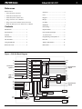
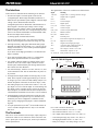
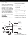
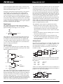
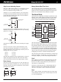
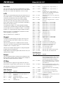
C-Programmable Controller
PK2100 Series
Introduction
The PK 2100 Series of C-programmable controllers is based on
the Zilog Z180 microprocessor. The PK2100 includes analog,
digital, serial, and high-current switching interfaces. The standard PK2100 includes a rugged enclosure with 2x20 LCD and
2x6 tactile keypad.
With the PK2100 Series you can detect contact closures, count
pulses, measure temperature, speed and pressure, control motor
speed, control proportional valves, switch fairly large currents,
and drive solenoids and external relays directly.
The PK2100 has a PLCBus expansion port, allowing you to
connect several Z-World expansion boards (such as the XP8100
or XP8300) if you need extra I/O. You can build networks of
controllers and communicate with modems. With Dynamic C
software and the PK2100’s LCD and keypad, you can easily
build operator interfaces.
TM
PK 2100 or PK2110, with enclosure, LCD, and keypad
The following PK2100 Series controllers are available:
With enclosure, 2x20 LCD, and 2x6 keypad.
Operates at 24V nominal.
PK2110
With enclosure, 2x20 LCD, and 2x6 keypad.
Operates at 12V nominal.
PK2120
No enclosure, LCD, or keypad.
Operates at 24V nominal.
PK2130
No enclosure, LCD, or keypad.
Operates at 12V nominal.
PK2100
The following PK2100 Series options are available:
• 9.216 MHz clock upgrade. (6.144 MHz standard)
• 128K flash (32K EPROM standard)
• 128K or 512K RAM (32K standard)
• Backlit LCD (with PK 2100 or PK2110)
Specifications
Board Size
5.5″ × 6.82″ × 0.78″.
Enclosure Size
5.5″ × 7.0″ × 1.6″.
Operating Temp.
–40°C to +70°C. With LCD, 0°C to 50°C.
Humidity
5% to 95% non-condensing.
Input Power
18–35VDC, 220 mA, linear supply [24V]
Processor
Z180
Clock
6.144 MHz [9.216 MHz optional]
Power Consumption
5.5W
PK2120 or PK2130, board-only
Features
•
•
•
•
•
•
•
•
•
•
2900 Spafford Street
Davis CA 95616 USA
Tel: +916.757.3737
Battery-backed static RAM, up to 512K bytes.
EPROM, up to 512K bytes, or flash memory to 256K bytes.
Battery-backed real-time clock (RTC).
Lithium backup battery, rated at 560 mA-hours. Since the
RTC and full 512K RAM draw about 16 µA, the battery will
sustain the RTC and RAM for about 4 years [35,000 hours].
Watchdog timer.
Power failure warning interrupt.
EEPROM, standard 512 bytes. Holds calibration constants for
the (2) DAC channels, among other data.
LCD. The standard screen has 2 lines of 20 characters. Other
displays can be installed on special order.
Keypad, 2 rows of 6 keys, for a total of 12 keys. The internal
interface provides for possible expansion to 24 keys using a
4 row x 6 column matrix.
Beeper with high- and low-volume.
Fax: +916.753.5141
www.zworld.com
Revision: A
PK2100 Series
Z-World 530-757-3737
2
References
Please refer to
• Z-World PK2100 schematic
• Z-World PLCBus data sheet
• Z-World Dynamic C data sheet
• Zilog Z180 MPU User’s Manual
• Zilog Z180 Serial Communication Controllers
• Zilog Z80 Microprocessor Family User’s Manual
Serial I/O ............................................... 6
LCD ....................................................... 7
Keypad ................................................... 7
Beeper .................................................... 7
I/O Map ................................................. 7
EEPROM ............................................... 8
Contents
Heatsinking ............................................ 9
Introduction ........................................... 1
Expansion Bus ....................................... 9
Specifications ........................................ 1
Power Failure Interrupts ........................ 9
Features ................................................. 1
12–Volt Version ..................................... 9
The Interface ......................................... 3
Programming with Dynamic C ............. 9
The Terminals ........................................ 3
Parts List .............................................. 10
Using the PK2100 ................................. 4
Jumpers and Headers ........................... 11
Real-Time Clock ................................... 6
Dimensions .......................................... 12
Figure 1. PK2100 Block Diagram
0
U1
1
U2
UEXP
DAC
DAC Output
K
2
U3
Universal
Inputs U4
O1
O2
O3
O4
O5
O6
O7
Real-Time Clock
3
4
U5
5
U6
High A/D–
Gain
Input A/D+
D1
D2
D3
D4
D5
D6
D7
Z180
6
Battery
•
•
•
•
•
RAM
Relay1
EPROM
7
Relay2
EEPROM
•
•
•
•
•
Digital
Input
High-Current
Output
NC1
com1
NO1
NC2
com2
NO2
Beeper
O8
O9
O10
High-Current
Output
+24V
PLCBus
C1
C1
Keypad
LCD
C2
C2B+
C2B–
Counter
Inputs
RS485/
RS422
Tx–
Rx–
Tx+
Rx+
RS232
Jack
PK2100 Series
Z-World 530-757-3737
3
The Interface
The signal names of the screw connectors are shown below.
A PK2100 Series controller has the following as its interface:
1 Six universal inputs. Universal inputs can be used as
(A) digital inputs. With a single threshold (in software or
hardware) the input channel yields a digital 1 when the input
voltage is above threshold and 0 otherwise.
(B) digital inputs with two thresholds. Z-World software returns a digital 1 when the input voltage is above a high
threshold, a 0 when voltage is below a low threshold, and reports ‘no change’ otherwise. It is a simple and logical extension to write software that handles several thresholds. Thus,
the universal inputs can be used as...
(C) analog inputs (with Z-World software).
The universal inputs accept 0 –10V with 10-bit resolution,
and are protected against overloads in the range ±48 volts.
2 One high-sensitivity (high-gain) differential analog input.
Normally, the high-gain input range is 0–1 volt, but you can
change resistors (R5, R11, RP5) on the operational amplifier.
It has 10-bit resolution.
If you don’t use the high-gain channel, a seventh universal
input is available.
3 Seven protected digital inputs, with a 2.5 volt threshold.
Three of the inputs also function as counter inputs.
4 Two counter channels capable of counting pulses at up to
600 kHz or more. The counter inputs can also be used to
measure pulse width and other pulse timing characteristics.
The counters use DMA hardware.
5 Two on-board relays, rated for 3A at 48V, with NO, NC, and
COM terminals for each. You can install MOVs to protect relay contacts.
6 Ten high-current outputs suitable for driving relays or solenoids. These outputs can sink approximately up to 500 mA
at voltages up to 48V (when used individually) subject to total heat dissipation restrictions for the driver chips (1.25W).
7 One analog output (DAC) which can be either a 0–10V voltage output or 0–20 mA current output. A second analog voltage output (UEXP), normally used by software to drive the
universal inputs, is available when the universal inputs have
a fixed hardware threshold. The DACs have 10-bit resolution.
8 An RS422/RS485 serial port and an RS232 serial port with
two handshaking lines operate at up to 38,400 baud. A second RS232 port can be configured as a substitute for the
RS485 port by changing board jumpers. It has no handshaking lines.
9 A 26-pin expansion bus (PLCBus ) for Z-World PLCBus devices or customer-designed devices. Refer to the PLCBus
data sheet.
Signal
+10V Ref
+5V
Meaning
Output from U11, analog reference voltage.
Output from 5V regulator
GND
Ground
U1–U6
Universal inputs
D1–D7
Digital inputs
C1A, C1B
Counter 1 inputs
C2A
Counter 2 input
C2B+, C2B–
Counter 2 inputs, differential
TX–,TX+
RS485 Transmit
RX–, RX+
RS485 receive
External power
+24V
K
Protection for high-current outputs O1–O7
High-current outputs
O1–O10
A/D–
Negative side of high-gain input
A/D+
(1) Positive side of high-gain input, or
(2) the seventh universal input
DAC
DAC output, 0–20 mA or 0–10 volts.
UEXP
Internal DAC, output is 0–10V.
NC, COM, NO Relay contacts for relays 1 and 2
Figure 2. PK2100 Signals
High-Gain Input
DC In
DAC Output
Relay1 Relay2
+10V ref
+5V
GND
U1
U2
U3
U4
U5
U6
GND
D1
D2
D3
D4
D5 /C1A
D6 /C1B
D7/C2A
GND
GND
Tx–
Tx+
Rx–
Rx+
C2B+
C2B–
+24V
K
GND
O1
O2
O3
O4
O5
O6
O7
O8
O9
O10
GND
A/D –
A/D +
DAC
UEXP
NC
COM
NO
NC
COM
NO
GND
Digital
Outputs
Universal
Inputs
Digital
Inputs
RS485 /
RS422 /
Diff.
Counter
TM
The Terminals
There are 50 screw terminals used for input, output, and power
connections. There are two connectors on the sides of the unit:
a RJ12 “phone jack” for the RS232 port, and a 26-pin connector
for the expansion bus.
For 12-volt versions of the PK2100,
• The connector labeled “+10V ref” is +7 volts.
• The connector labeled “+24V” is +12 volts.
• DAC output (either channel) is not 0–10V, but 0–7V.
• Universal input range (any) is not 0–10V, but 0–7V.
• The high-gain channel is not 0–1V, but 0–0.7V.
• Relay coil voltage is 12V. Relay rating is 5A/120V.
PK2100 Series
Z-World 530-757-3737
Using the PK2100
Universal Inputs
Figure 3 below shows the six universal inputs and the high-gain
input. A seventh universal input is available if you do not use
the high-gain channel. (Note that the high-gain input is channel
6 and that the “spare” universal input is channel 7.)
Each input channel has a comparator that yields a 1 when the
input level is greater than a threshold, and 0 otherwise.
By placing a jumper at J9, you can (1) choose the fixed hardware threshold (1.6V by default) or (2) use the internal DAC to
generate a threshold. When software generates the thresholds
using the DAC, you can compare inputs against as many thresholds as you like. Z-World software compares against 1 or 2
thresholds for digital input; it compares against several thresholds for analog input (using successive approximation).
Channel 5 (labelled U6) can be 4-20 mA current loop if you
connect pins 7 and 8 of H5.
The internal DAC channel usually generates the reference voltage for the inputs. However, if you connect the fixed hardware
reference at jumper J9, this DAC channel is available at UEXP
on the screw terminals.
High-Gain Analog Input
This input is useful for devices requiring higher input sensitivity, for example, thermistors or RTDs in a bridge. The input
4
range is 0–1.0V with 10-bit resolution. The gain at the plus and
minus inputs is 10 when jumper H7 is installed. If H7 is removed, then the gain of the plus input becomes higher: 11. The
calibration gain and offsets are stored in the EEPROM.
The gain, when H7 is connected is
y = a1 × (x1 + a0) – b1 × x2
[1]
where
a1 is the positive side scale.
a0 is the positive side offset.
b1 is the negative side scale.
x1 is the positive side input.
x2 is the negative side input.
Note that b1 = a1 – 1 (with H7 not connected). If the negative
input x2 is tied to ground, then the equation becomes
y = a1 × (x1 + a0)
[2]
or, solving for x1,
x1= y /a1 – a0
[3 ]
This equation returns the input voltage, given the reading.
Solving equation 1 for (x1–x2) in terms of y and x1 yields
(x1–x2) = y/b1 – (a1/b1 – 1) × x1 – a0 × a1 /b1
[4 ]
If you want to change the gain of the high-gain input, change
R5, R11, and possibly RP5. These are factory set to 47K, 47K,
and 470K for a factory gain of 10 (or 11, if H7 is removed).
When differential inputs are desired, it is preferable to operate
with H7 removed, since the scaling difference between the
+10 volt reference
3.3K
Jumper H4 to H6 to pull up
Channels 0–5,
labelled U1–U6
RP4
+
UINx
22K
Jumper H5 to H6 to pull down
0.01µ
–
10K
reading to U8 or U9
I/O address is UINP bits 0–5
comparator
LM339A
4.7K
RN6
10K
430Ω resistor, 4–20 mA loop,
channel 5 (U6) only. Connect H5:7–8
1.6V
R28
RR
5.1K
DAV/R
V/EXP
+
DAC
U22
.....
DACI0
–
UEXP
J9
R23
+
+10 volt ref
10K
reading to U30
22K
0.01µ
H1
RP6 a
10K
R11
AIN+
R5
RP5 b
470K
H7
–
I/O address is DREG2, bit 7
comparator
LM339A
op-amp
LM324A
+
RP6 b
–
10K
47K
AIN–
47K
Channel 7,
labelled AD+
op-amp
LM324A
+
–
RP5 a
470K
100 pF
SOUT
10K
reading to U9
comparator
LM339A
IO address is UINP bit 6
Channel 6, highgain, not labelled
Figure 3. Universal Inputs and High-Gain Channel
PK2100 Series
Z-World 530-757-3737
positive and negative inputs will be exactly 1 and will not depend on a balance between resistors, making the output 5 volts
when both differential inputs are 5 volts.
If the gain is increased, it becomes necessary to use an operational amplifier with a more stable offset voltage than the
LM324, which has considerable drift over temperature. The
Linear Technology LM1014 is suitable for gains up to 100 or
more. The negative input has a low input impedance compared
to the positive input (when H7 is removed). If R5 is decreased
to increase the gain, this impedance becomes even lower. When
a bridge is used, the finite impedance of the negative input has
the effect of changing the gain slightly.
Digital Inputs
The 7 digital inputs accept an input voltage with a digital
threshold at approximately 2.5 volts. The inputs are protected
against overload over the range of – 48 to +48 volts.
+5V
10k
22k
Input
Digital Input
low-pass
filter
0.01 µF
These inputs are convenient for detecting contact closures or
sensing devices with open collector transistor outputs. Logic
level outputs can also be detected if they are supplied from
CMOS logic outputs which are guaranteed to swing to at least
3.5 volts. Three of the digital inputs (D5–D7) also function as
inputs to the high speed counters.
Counter Inputs
Three of the digital inputs also serve as counter inputs. There
is, in addition, a special differential counter input. The counter
inputs are arranged as shown here:
The counters use the DMA channels of the Z180. The maximum
counting speed is approximately 600 kHz. The DMA channel
can be programmed to store a byte from an I/O port to memory
for each count, if desired. This byte can be the least significant
byte of the internal programmable counter (PRT) which allows
the count edge to be localized in time. This feature can also determine the exact time, within a few microseconds, at which an
event occurs by programming the DMA channel to store one
byte and then interrupt. The interrupt routine can read the most
significant part of the PRT counter and any software extension
of this counter. In general, the maximum count is 65,536 which
can be extended by software to larger counts if the counting
speed is not higher than about 10 kHz.
The capabilities of the counter are summarized as follows:
1 Measure the time at which a negative edge occurs with a
precision of a few microseconds. The measurement can be
repeated hundreds of times per second. A minimum time
must occur between successive events to allow for interrupt
processing.
2 Measure the width of a pulse by counting (up to 65,536) at a
rates from 600 kHz to 300 Hz.
3 Count negative-going edges for each two channels. The
maximum count for high-speed counting (5 kHz to 600 kHz)
is 65,536. For low speed counting, the maximum count not
limited by hardware.
Analog Output
One analog output (named DAC) is provided. The output can be
either a 0–10V (connect jumper J7:2-3) voltage output or a 0–20
mA current output (connect J7:1-2) suitable for driving 4–20
mA current loops. It will drive 20 mA up to 470 ohms. The
resolution is 10 bits.
324
+
DAC8, U29
+5V
8
D[0–7] 8
C1A
D0
A[0–2]
+5V
5
273
U24
259
U31
10K
U27C
470K
–
BITS OUT
+
BIT[9-2] MSB
820K
1640K
Current
U27B
10
–
100p
BIT[0] LSB
BIT[1]
J7
324
DAC
Voltage
100p
3.9K
10K
470K
/DREQ0
Counter 1
C1B
+5V
J8 : 7-8
CKA1
J8:9-10
C2A
/DREQ1
C2B+
+
C2B–
U34
C2B
–
Differential receiver
Counter 2
The counters sense negative edges. The differential receiver input can be used as a digital input by attaching one side of it to
the desired threshold voltage. It can be used as a true differential input for such devices as inductive pickups. It has a common mode voltage range from –12 to +12 volts with an input
hysteresis of 50 millivolts. An internal jumper can connect the
signal CKA1 which is controlled by the serial port hardware. It
can be set to various speeds from 600 kHz down to 300 Hz.
An 8-bit DAC chip, a network of resistors, and LM324 op-amps
produce the output. Software writes the 10-bit output value to
three registers:
DAC
0x90
0xA2
0xA3
Which bits
Bits 9–2
Bit 1
Bit 0
UEXP
0x88
0xA0
0xA1
Another 10-bit analog output channel (UEXP) is available if it is
not used to provide reference voltage for the universal inputs. It
produces 0–10V with 10-bit resolution.
DAC8, U22
8
D[0–7] 8
D0
A[0–2]
273
U28
259
U31
BITS
+
OUT
–
BIT[9-2] MSB
BIT[0] LSB
BIT[1]
324
U27A
820K
1640K
UEXP
100p
3.9K
Note that UEXP is not identical to the first DAC channel.
PK2100 Series
Z-World 530-757-3737
6
High-Current Switching Outputs
Battery-Backed Real-Time Clock
There are 10 high-current outputs O1–O10 available at external
terminals. Seven of the outputs belong to one high-current
driver (U26) and three belong to another (U35).
The real-time clock stores a representation of time and date,
and runs independently. The RTC can be programmed to interrupt the processor periodically through the INT2 interrupt line.
Please refer to the Toshiba TC8250 data book for detail.
Outputs O1–O7 use a common connector (“K”) for the protective diodes. All loads connected to the same driver chip must
use the same power supply so the diodes can return inductive
spikes to the same power supply.
your
inductive
load
your external power
supply, e.g. 48V
The Serial Ports
The Z180 has two independent, full-duplex asynchronous serial
channels, with a separate baud rate generator for each channel.
The baud rate can be divided down from the microprocessor
clock, or from an external clock for either or both channels.
microprocessor internal bus
K
interrupt request
A digital output
channel, O1–O7
TXA0
If you use the PK2100’s on-board power supply (+24V or +12V
nominal) for your load, you should route K to it by connecting
jumper H11, as shown:
+24V
+24V
your
inductive
load
H11
RXA0
Transmit Data
Reg: TDR0
Transmit Data
Reg: TDR1
Transmit Shift
Reg: TSR0
Transmit Shift
Reg: TSR1
Receive Data
Reg:RDR0
ASCI
Control
Receive Data
Reg:RDR1
Receive Shift
Reg: RSR0
Receive Shift
Reg: RSR1
RTS0
Control Register A:
CNTLA0
Control Register A:
CNTLA1
CTS0
Control Register B:
CNTLB0
Control Register B:
CNTLB1
DCD0
Status Register:
STAT0
Status Register:
STAT1
TXA1
RXA1
CTS1
K
A digital output
channel, O1–O7
The diodes for outputs O8–O10 use the on-board power supply
directly.
The driver used is the ULN2003 (Texas Instruments). Each
driver chip can dissipate a maximum of 1.25 watts when the
ambient temperature is 60°C. Each output consumes power, depending on the current, as follows:
100 mA
200 mA
350 mA
0.10 watt
0.25 watt
0.50 watt.
This limits the maximum current to approximately 150 mA per
output if all outputs are turned on at the same time continuously. The maximum current for any single output is 500 mA.
Relay Outputs
There are two SPDT relays rated at 3A, 48 volts. The three contacts for each relay have terminals (NC, NO, COM on the terminal strips). You have the option to install MOVs on the board to
protect the relay contacts.
M4
M5
M2
NC1
NC2
C1
NO1
C2
NO2
M3
CKA0
Baud Rate Gen. 0
CKA1
Baud Rate Gen. 1
The serial ports have a multiprocessor communications feature
that can be enabled. When enabled, an extra bit is included in
the transmitted character (where the parity bit would normally
go). Receiving processors can be programmed to ignore all received characters except those with the extra multiprocessing
bits enabled. This provides a 1-byte attention message that can
wake up a processor without the processor having to monitor
(intelligently) all traffic on a shared communications link.
The serial ports can be polled or interrupt-driven. Normal serial
options are available: 7 or 8 data bits, 1 or 2 stop bits, odd, even
or no parity, and parity, overrun, and framing error detection.
Port 0
Port 0 is RS232; its connector is the RJ12 jack. It has CTS and
RTS handshaking lines. Port 0 is constrained by hardware to
have the CTS (clear to send) pulled low by the RS232 device
with which it is communicating.
If the device with which the port is communicating does not
support CTS and RTS, the CTS and RTS lines on the PK2100
side can be tied together to make communication possible.
Port 1
Port 1 is RS485 normally, with transmit and receive lines on the
screw terminals. You can use port 1 as an RS232 port, but it has
no CTS/RTS handshaking.
PK2100 Series
Z-World 530-757-3737
0x85
0
KEYR3
0x86
0
KEYR1
0x87
0
KEYR4
The 2×20 LCD used with the PK2100 can come from one of several vendors. All the LCDs are identical in operation, electrical
connections, and dimension. They may differ in timing.
0x88
0–7 UEXP
0x90
0–7 DAC
An LCD can take up to 1600 µs to carry out an operation.
Therefore it provides a busy flag, which you may read at address LCDRD (0xD0). It is an error to send other commands or
data to an LCD while it is busy.
0x98
0
BEEPL
0x99
0x9A
0x9B
0x9C
0x9D
0x9E
0x9F
0xA0
0xA1
0xA2
0xA2
0xA4
0xA5
0xA6
0xA7
0xC8
0xCA
0xCC
0xCE
0xD8
0xD9
OxE0
0xF0
0
0
0
0
0
0
0
0
0
0
0
DRV1
DRV2
DRV3
DRV4
DRV5
DRV6
DRV7
UEXPA
UEXPB
DACA
DACB
DRV8
DRV9
RLY1
RLY2
BUSADR0
BUSADR1
BUSADR2
BUSWR
LCDWR
LCDWR+1
RTRW
RTALE
Baud Rates
The Z180 serial ports can generate standard baud rates. When
the clock is 6.144 MHz, rates range from 150 to 38.4 kHz. When
the clock is 9.216 MHz, rates range from 75 Hz to 19.2 kHz.
LCD
To communicate with the LCD, send commands to address
LCDWR (0xD8). Command values are built into the command.
To write data to the LCD, use address LCDWR+1. To read data
from the LCD, except for the busy flag, use address LCDRD+1.
Refer to any of the LCD manufacturers’ data sheets for information regarding LCD operations.
The LCD connector is a 2×7 header, P2.
Keypad
To read the 2×6 matrix keypad, you “drive” the row or rows
you wish to sample, then read the columns. Any or all keys
may be sensed.
There are four keypad “rows” at addresses KEYR1–KEYR4
(0x86, 0x81, 0x85, 0x87 respectively) and six keypad columns
readable as bits 2–7 of DREG1 (0x81).
The PK2100 can address four keypad rows, but presently there
is support only for 2 keypad rows.
Jumper block J4 uses keypad signals (/KH2, and KV1–KV3) for
operation mode settings.
Beeper
The on-board beeper has two volume levels. Alternately send 1
then 0 to make it oscillate. Write to BEEPH (0x83) for high volume. Write to BEEPL (0x98) for low volume.
Addr
Bit Symbol
0x80
0–7 UINP
The internal Z180 I/O registers occupy the first 64 (0x40) addresses of the I/O space. Refer to the Z180 MPU User’s Manual.
0x88
The following I/O addresses control the PK2100 devices which
are external to the Z180 processor.
0x98
Write Registers
Addr
Bit Symbol
Function
0x80
0x81
0
0
SDA_W
KEYR2
0x82
0x83
0
0
ENB485
BEEPH
0x84
0
SCL
EEPROM data, write.
Keypad drive row 2. Open collector, “1”
drives low.
Enable RS485 channel
Beeper, high-voltage drive. “1” drives
beeper.
EEPROM clock.
Keypad drive row 3. Open collector, “1”
drives low.
Keypad drive row 1. Open collector, “1”
drives low.
Keypad drive row 4. Open collector, “1”
drives low. Also, tenth high-current output
(DRV10) if key row not used.
Internal DAC, bits 9-2. See also UEXPA and
UEXPB below.
External DAC, bits 9-2. See also DACA and
DACB below.
Beeper, low-voltage drive drive. “1” drives
the beeper.
Digital output 1. “1” drives output.
Digital output 2. “1” drives output.
Digital output 3. “1” drives output.
Digital output 4. “1” drives output.
Digital output 5. “1” drives output.
Digital output 6. “1” drives output.
Digital output 7. “1” drives output.
Internal DAC, bit 1.
Internal DAC, bit 0.
External DAC, bit 1.
External DAC, bit 0.
Digital output 8. “1” drives output
Digital output 9. “1” drives output
“1” enables relay 1.
“1” enables relay 2.
Expansion bus, first address byte
Expansion bus, second address byte
Expansion bus, third address byte
Expansion bus write to port
LCD write register, control
LCD write register, data
Real time clock, read/write data registers
Real time clock, write address latch
Read Registers
0x81
I/O Map
0
0
0
0
0– 7
0– 7
0– 7
0– 7
0– 7
0– 7
0– 3
0– 3
7
0xC0
0xC2
0xC4
0xC6
0xD0
0xD1
Function
Bits 0–6 are universal inputs 0–5 and the
high-gain analog input (bit 6). Bit 7 is PR, a
user-programmable jumper (J8 pins 11-12)
and is low when the jumper is installed.
0–7 DREG1
Bit 0 is EEPROM data bit. Bit 1 is NMI interrupt line (power fail line). Bits 2–7 are keypad columns 0–5.
0–7 DREG2
Bits 0–6 are digital inputs 0–6. Bit 7 is the
universal input channel fed through AD+ (or
universal input channel 8).
— WDOG
Reading this location “hits” the watchdog
timer.
0–7 BUSRD0
First read, data port of expansion bus
0–7 BUSRD1
Second read, data port of expansion bus
0– 7 —
Unused bus read address
— BUSRESET Read this location to reset all devices on the
expansion bus.
0–7 LCDRD
LCD read register, control
0–7 LCDRD+1 LCD read register, data
PK2100 Series
Z-World 530-757-3737
Interrupt Vectors
0x10E
Most of the interrupt vectors can be altered under program control. These are the suggested and default vectors:
0x110
Addr
Name
0x00
0x02
INT1_VEC
Expansion bus attention INT1 vector.
INT2_VEC
INT2 vector, can be jumpered to output of
0x04
0x06
0x08
0x0A
0x0C
0x0E
0x10
PRT0_VEC
PRT1_VEC
DMA0_VEC
DMA1_VEC
CSIO_VEC
SER0_VEC
SER1_VEC
Description
the real-time clock for periodic interrupt.
PRT timer channel 0
PRT timer channel 1
DMA channel 0
DMA channel 1
Clocked serial I/O
Asynchronous Serial Channel 0
Asynchronous Serial Channel 1
0x11C
0x128
0x12A
0x130
Jump Vectors
0x146
Instead of loading the address of the interrupt routine from the
interrupt vector, the following interrupts cause a jump directly
to the address of the vector, which will contain a jump instruction to the interrupt routine. For example,
0x15C
0x66
0x08
0x38
non-maskable power-failure interrupt
INT0, mode 0
INT0, mode 1
0x15E
Interrupt Priorities from Highest to Lowest
Internal Trap (Illegal Instruction)
External
NMI
(non maskable interrupt, power failure)
External
INT0
(non-maskable, level 0)
External
INT1
(non-maskable, level 1, expansion bus attention line)
External
INT2
(non-maskable, level 2)
Internal
PRT timer channel 0
Internal
PRT timer channel 1
Internal
DMA channel 0
Internal
DMA channel 1
Internal
Clocked serial I/O
Internal
Serial Port 0
Internal
Serial Port 1
0x160
EEPROM
The parameters given here apply to the standard 24-volt
PK2100. See The 12-Volt PK2100 (page 9) for changes relating
to the 12-volt version.
Addr.
Definition
0x000
Startup Mode. If 1, enter programming mode. If 8, execute
loaded program at startup.
Baud rate in units of 1200 baud.
Unit “serial number.” BCD time/date with the following format: second, minutes, hours, day, month, year.
Required power voltage. This value is 24 for standard
PK2100s and 12 for the 12-volt version.
Software test version (times 10). For version 1.2, this is 12.
Microprocessor clock speed in units of 1200 Hz (16-bits).
For 6.144 MHz clock speed, this value is 5120.
Bus address for networking. 16 bits.
0x001
0x100
0x106
0x107
0x108
0x10C
0x164
0x168
0x16A
0x16C
8
Analog voltage reference units of 1 millivolt. 16 bits. 10300
for 10.300 volts.
Excitation resistor values for universal inputs 1–6. These are
the pull-up resistors to the +10V reference. Six integers in
units of 0.5 ohm. 6600 for 3.3K resistors.
Pull-down resistor values for universal inputs 1–6. Six integers in units of 0.5 ohm. 9400 (4.7K ohms).
4–20 mA load resistor. Resistance in units of 1/2 ohm. The
nominal value is 780 (2 counts/ohm x 390 ohms). This represents the combined resistance of the load resistor and the
pull-down resistor in parallel.
Reserved
11 values relating to internal DAC. First value is output voltage when nominal output is zero. Additional values are output voltage increment (above offset) when input value is 1,
2, 4... 256, 512. Stored as integers expressed in 0.5 millivolt
units.
11 values relating to external DAC. First value is output voltage when nominal output is zero. Additional values are output voltage increment (above offset) when input value is 1,
2, 4... 256, 512. Stored as integers expressed in 1/2 millivolt
units.
For the standard PK2100, this is current in units of 0.001 mA
corresponding to voltage output of 2.000V when is set for 020 mA output into nominal 392 ohm load resistor. Typically,
near 4000. For the 12-volt PK2100, the output range is 0-15
m A.
For the standard PK2100, this is current in units of 0.001 mA
corresponding to voltage output of 10.000 volts when is set
for 0-20 mA output into nominal 392 ohm load resistor. For
the 12-volt PK2100, the output range is 0-15 mA.
With shorting jumper H7 connected, these are 16-bit numbers a0 and a1 high-gain plus-side inputs in the gain formula
y = a1 x (x1 + a0)
with the minus side grounded. If the minus side is not
grounded, the formula is
y = a1 x ( x1 + a0 ) – b1 x x2.
where b1 is the minus-side gain and can be computed from
the calibration constants stored at location 0x164. The value
y is the output of the high-gain amplifier read with universal
input channel 7. The value x1 is the plus-side input read
with universal input channel 8 and x2 is the minus-side input.
The coefficient a0 is signed and is in units of 0.01 mV. The
coefficient a1 is the unsigned dimensionless gain expressed
in units such that a gain of 10 is equal to 2000.
With shorting jumper H7 removed, these are 16-bit numbers
a0 and a1 high gain plus-side input in the gain formula
y = a1 x (x1 + a0)
with the minus side grounded. If the minus side is not
grounded, the formula is
y = a1 x ( x1 + a0 ) – b1 x x2.
where b1 is the minus-side gain and can be computed as
a1–1.
Reserved
Resistance of excitation resistor for high-gain plus input in
ohms. Nominal value 10K. An unsigned integer.
Long coefficient relating speed of microprocessor clock
relative to speed of real-time clock. Nominal value is
107, 374,182 which is 1/40 of a second microprocessor clock
time on the scale where 232 is 1 second. This requires 4
bytes of EEPROM, stored least byte first.
PK2100 Series
Heat Sinking
A PK2100 Series controller has two power supply regulators.
The aluminum enclosure provides the heat sink. In the boardonly version, the mounting rails provide the heat sink. The +5V
regulator dissipates the most heat and transfers heat to the case
or side rails via two mounting “pem” nuts. Maximum heat dissipation by this regulator is 10W when the ambient temperature
is 50°C. If an attempt is made to dissipate more heat because of
a combination of high input voltage or excessive current draw
on the +5V supply, the regulator will shut down protectively.
Power dissipation is given by the formula:
Z-World 530-757-3737
9
2 A system reset is triggered when the regulated +5V supply
falls below 4.5 volts. The reset remains enabled as the voltage falls further. At some point, the chip select for the SRAM
is forced high (for standby mode). The time/date clock and
SRAM are switched to the lithium backup battery when VCC
falls below the battery voltage of approximately 3 volts.
The 12-Volt PK 2100
The following are changes for the 12-volt PK2100. Note that
R40 and U12 are absent on the 12V board, and R9 is 14K, not
22K. The 12V board has 12V relays, nominally 5A, 120V.
P = (VIN – 5) × (I + 0.15)
Subsystem
Effect
VIN = input voltage
External DAC
The external DAC voltage output (when J7 connects pins 2–3) is reduced to 0–7 volts. The current
output (J7 connects pins 1–2) is now 0–15 mA.
The internal DAC voltage output (UEXP) is reduced to 0–7 volts. This directly affects the universal input channels, since the incoming value is
compared against the UEXP output.
Because of the change in the internal DAC (UEXP)
output, the universal input channels read a nominal range of 0–7V.
The effective input range to 0–700 mV.
I = current, in amperes, drawn from +5V supply by external
accessories on bus or from VCC terminal.
Internal DAC
Environmental Temperature Constraints
No special precautions are necessary over the range of
0–50°C (32–122°F). For operation at temperatures much below
0°C, the PK2100 should be equipped with a low temperature
LCD which is specified for operation down to –20°C. The heating effect of the power dissipated by the unit (about 5 watts)
may be sufficient to keep the temperature above 0°C, depending on the insulating capability of the enclosure used. The LCD
storage temperature is 20°C lower than its operating temperature, which may protect the LCD in case the power should fail,
removing the heat source. The LCD unit is specified for a maximum operating temperature of 50°C. Except for the LCD, which
fades at higher temperatures, the PK2100 can be expected to operate at 60°C, or more, without problem.
Universal Inputs
High-Gain Input
EEPROM changes for the 12V system
Addr
Meaning
0x106
0x15C
Required power. This value is 12 for the 12-volt version.
For the 12-volt PK2100, this is current in units of 0.001 mA
corresponding to voltage output of 2.000V.
For the 12-volt PK2100, this is current in units of 0.001 mA
corresponding to voltage output of 10.000 volts.
0x15E
Other EEPROM values remain unchanged.
Expansion Bus
The PLCBus, is a general purpose expansion bus for Z-World
controllers. Z-World currently sells the following expansion devices. The list may change:
TM
Device
Description
XP8100
Several options of 16 or 32 protected digital I/O lines. Some
versions have optical isolation.
16 “universal inputs,” 6 high-current switching outputs
Six SPDT power relays
Contains eight DIP relays, each SPST, NO.
11 12-bit A/D converters (4 with signal conditioning)
2 DACs
1 full-duplex RS232 channel
Stepper motor controller (based on PCL-AK)
XP8200
XP8300
XP8400
XP8500
XP8600
XP8700
XP8800
Multiple expansion boards may be daisy-chained together and
connected to a Z-World controller to form an extended system.
For details, refer to the PLCBus data sheet.
Power Failure Interrupts
The following events occur when power fails:
1 The power-failure NMI (non-maskable interrupt) is triggered
when the unregulated DC input voltage falls below approximately 15.6 volts (subject to the voltage divider R9/R33).
[7.8V on 12V systems]
Reference Voltage
The reference voltage (marked +10V on the terminal connector)
is nominally +7 volts. This affects all subsystems using this
value as a reference, as described below.
Programming
Developers program a PK2100 Series controller by connecting it
to the serial port of an IBM PC running Z-World’s Dynamic C
development system. Serial communication for programming
takes place at 19,200 baud or at 38,400 baud. While a program is
undergoing development, the controller normally remains connected to the PC and Dynamic C.
Once program development is complete, the completed program can reside in one of the following places:
• Battery-backed RAM.
• ROM which is written on a separate ROM programmer and
then substituted for the standard Z-World ROM.
• Flash memory which may be programmed or reprogrammed
without removing it from the controller.
Programmers generally use Dynamic C function libraries. Dynamic C libraries support direct I/O and virtual I/O (which is
easier but slightly less efficient). The virtual driver is a system
function that monitors the PK2100 I/O lines, every 25 millisec-
PK2100 Series
onds. The programmer reads and writes to virtual registers as
variables, and does not contend with the hardware details.
Initial PK 2100 Setup
When the PK2100 powers up, it consults its board jumpers, the
keypad if any, and the contents of the EEPROM to determine its
mode of operation. The modes of operation are the following:
• Run a program stored in battery-backed RAM.
• Prepare for Dynamic C programming at 19.2K baud using
the RS232 port (“phone” jack).
• Prepare for Dynamic C programming at 38.4K baud using
the RS232 port.
If your controller has a keypad, you can use it to select the operation mode. Hold down the menu/setup key and one other
key simultaneously (field/run, up/pgm 19.2, or down/pgm 38.4).
The unit will beep to acknowledge the change of operating
mode. In unusual instances, you might also need to cycle
power while holding the key combination.
If the keypad is not available, or you want to override the keypad, use the jumper block J4.
Connecting the PK 2100 to your PC & Dynamic C
1 Connect the red-tagged lead from your 24V (or 12V) powersupply to the +24V screw connector. Connect the other
power supply lead to the GND screw connector.
2 Plug the serial programming cable into the PK2100 jack and
connect it to a PC serial port.
3 Plug the PK2100’s power supply into a wall socket. Start Dynamic C.
Software Drivers
Z-World software includes the functions listed here.
Digital Input/Output
• void up_setout( int channel, int value )
• void up_digin( int channel )
Analog Output
• void up_daccal( int value )
• void up_dacout( int rawval )
• void up_expout( int rawval )
• void up_dac420( int current )
Analog Input
• void up_adcal( int channel )
• void up_in420()
• void up_adrd( int channel )
• void up_adtest( int channel, int testval )
• void up_uncal( int calval )
• void up_docal( int calval )
• float up_higain( int mode )
High Speed DMA Counter
• void DMA0Count( uint count )
• void DMA1Count( uint count )
• uint DMASnapShot( byte channel, uint *counter )
Z-World 530-757-3737
EEPROM Read / Write
• int ee_rd( int address )
• int ee_wr( int address, char data )
• int eei_rd( int address )
Flash EPROM Write
• int WriteFlash( ulong addr, char* buf, int num )
Parts List
Listed are major parts. Resistors, capacitors and other small
parts may be found on the schematic.
B3
BZ1
H1
H4
H5
H6
H7
H8
H9
H11
J1
J3
J4
J7
J8
J9
J11
JP1
JP2
JP3
K1
P1
P2
SW1
U1
U2
U3
U4
U5
U6
U7
U8
U9
U10
U11
U12
U13
U14
U15
U16
U17
U18
U19
U20
U21
U22
Battery, 3V, 560 mA-H
Buzzer
1x9 Header, .100″
1x6 Header, .100″
1x8 Header, .100″
2x6 Header, .100″
1x9 Header, .100″
2x3 Header, .100″
1x9 Header, .100″
2x1 Header, .100″
1x14 Header, .100″
1x3 Header, .100″
1x8 Header, .100″
1x9 Header, .100″
2x7 Header, .100″
1x3 Header, .100″
1x3 Header, .100″
Phone Jack RJ12
Terminal strip 25x
Terminal Strip 25x
Keypad flex connecter
2x13 Header for PLCBus
2x7 Header, .100″
2x1 Header, .100″
EPROM and socket, 32K
SRAM, 32K, 70ns
Octal 3-state transceiver, 74HC245
Octal 3-state transceiver, 74HC245
EEPROM, 512, 24C04
PAL (for PK2100)
Dual decoder 2:4, 74HC139
Quad 2:1 mux, 74HC257
Quad 2:1 mux, 74HC257
Watchdog, 691
Adjustable Reg, 723, 150mA
Linear Reg, 7805, 15V, TO-220
Switching Reg, 7662
8-bit addressable latch, 74HC259
Real-Time Clock, Toshiba 8250
Z180
Hex inverter, open drain, 74HC05
Quad 2-in OR, 74HC32
Quad 2-in OR, 74HC32
Linear Reg, 7805, 5V, TO-220
Comparator, 339
8-bit DAC
10
PK2100 Series
U23
Z-World 530-757-3737
Connect jumper to cause differential inputs AD+ and AD– to
be balanced in gain. If H7 is disconnected, the gain is greater
on the AD+ side so that if both inputs are set to 5 volts, the
output of the operational amplifier is 5 volts. Use this feature
for accepting input from bridges where the taps are nominally
at +5V.
1-2 Connect to enable a second RS232 output (at the expense
of RS485 output) The output pin will be TX–. The RS232
input will be RX–. RX+ must be tied to ground.
3-4, Connect these positions to enable the termination
5-6 and bias resistors for RS485 communications.
When installed, this connects the on-board battery to relay 1
N.O. contact. Use H9 when a battery self-test circuit is to be
implemented by connecting a switched load to the battery.
Normally installed. Connects “K” to +24V power supply. Disconnect only if a separate power supply is to be used for
high-current outputs O1–O7. In that case, K must be connected to that power supply.
1-2
Connect if using 32K RAM or 128K RAM
2-3
Connect for 256K or 512K RAM
4-5
Connect if using 32K, 64K, or 128K EPROM
5-6
Connect for 512K or 256K EPROM
7-8
Connect for other than 32K EPROM
8-9
Connect for 32K EPROM
12-13 Connect for 64K, 128K, 256K flash EPROM
13-14 Connect for 512K (non-flash) EPROM
This is the operation mode jumper. By software convention,
position 7-8 means “enter programming mode at 19.2K baud.”
Position 6-7 means “run the program in memory.” Position 2-3
means “enter programming mode at 38.4K baud.” J4 overrides
the keypad when a readable jumper is installed.
H7
8-bit addressable latch, 74HC259
Octal FF w clear, 74HC273
Diff. Bus transceiver, 75176A
7-chan sinking HC driver, 2003
Opamp, 324
Octal FF w clear, 74HC273
8-bit DAC
Octal 3-state buffer, 74HC244
8-bit addressable latch, 74HC259
Comparator, 339
RS232 driver 1488
Diff. Receiver, 75175
7-chan sinking HC diver, 2003
12.288 MHz crystal for 6.144 MHz system]
32,768 Hz crystal
Linear reg, 79L05, –5V
U24
U25
U26
U27
U28
U29
U30
U31
U32
U33
U34
U35
X1
X2
Z1
H8
H9
H11
J1
Jumpers and Headers
Headers and jumpers are shown in the drawing below. Pin 1 positions are indicate by “+” markers.
H1
H5
H6
When connected, a 10K excitation resistor RP6A is connected
between the +10V reference and the high-gain input AD+.
7-8 Connect to engage 4–20 mA load resistor (430 ohm) from
universal input 6 to ground.
For universal input n (1–6), connect H6-n to H4-n to engage
excitation resistor (3.3K) to +10 volt reference. Connect H6-n
to H5-n to engage pull-down resistor (4.7K).
J4
JP3
LED
J7
H1
U26
U12
PLC Bus Connector
LCD
Reg.
U3
REL2
U35
HC Driver
U23
U11
HC Driver
U31
Latch
U27
Op-Amps
Latch
REL1
H7
Relay
Relay
H9
H1
U20
PLCBus
F1
U29 DAC
U22 DAC
D1
U2
RAM
P2
U24 Flip Flops
28- / 32-pin positions
P1
U4
U6
PLC Bus
J1
PAL
EE
U10 691
X1
U16
EPROM
U18 OR
U32
Comp.
U9
U8 MUX
MUX
U13
U17
U33 RS232
U7
U30
U15
K1
JP1
NOT
U14 Latch
H5
H6
H4
Z1
28- / 32-pin positions
Z180
Comp.
Battery
D2
U1
J3
J9
U28 Flip Flops
J8
U5
Beeper
U21
11
Buffer
MUX
Phone
Jack
U25
U34 RS485
U19 OR
RTC
J11
SW1
J4
Keypad Conn.
H8
JP2
Figure 4. Parts
Locations
PK2100 Series
J7
J8
J3
J9
Z-World 530-757-3737
Connect 2-3 for voltage output on the DAC channel (factory
setting). Connect 1-2 for 20 mA current output.
1- 2
Enable switching power supply
3- 4
Connects timer output T0 to processor /INT2.
Can generate periodic interrupts.
5- 6
Connects universal input 1 to processor /INT0.
Not recommended.
7- 8
Connect processor I/O CKA1 to digital input 6.
9-10
Connect processor I/O CKA1 to digital input 7.
11-12 Processor-readable jumper. By convention, install
whenever 13-14 is installed.
13-14 Install jumper to enable watchdog timer.
1- 2
Protect EEPROM against writes at addresses 256–511.
This is the factory setting.
2- 3
Allow EEPROM writes at addresses 256–511.
1- 2
The comparators used for the universal inputs are
connected to the voltage divider RR which has a
value of 1.6 volts. This causes the universal inputs to
have a threshold fixed at this value.
2- 3
J11
1-2
2-3
12
Factory setting, where the internal DAC is connected
to the comparators used for the universal inputs.
Connect to enable CTS on the RS232 port (0).
Connect to use the CTS line as a board reset line. CTS
high will reset the PK2100 board.
Board Dimensions
The drawing below shows board dimensions, mounting hole locations and sizes, all the jumpers and headers, pin 1 positions
for important headers, and the positions of resistors that affect
the universal inputs and the high-gain input. Mounting holes
are (0.225, 0.7) from the extreme corners of the board. Resistors
R5, R11, and resistor pack RP5 affect the high-gain channel. Resistor R28 (5.1 kΩ) is part of a resistor divider that gives the optional fixed hardware reference voltage for the universal inputs.
Maximum height of components above the board is 0.65″ approximately. Overall height is 0.78″ approximately.
Figure 5. Board Dimensions
6.53
0.53
JP3
H11
R11
U27
0.16 dia
R5
P2 (1.19, 4.13)
RP5
J7
LED
H7
H9
H1
0.25 dia
to LCD
P1
(0.53, 2.66)
5.5
J1
J8
4.5
“Phone
Jack”
J3
J9
JP1
R28
H5
H6
J4
1.77
0.17 dia mounting holes, 4x
to keypad (flex cable)
H8 J11
K1
2.73, 0.68)
SW1
0.4 typ
0.7 typ
H4
JP2
0.91 typ
6.82
~0.7
~0.6
0.225 typ
PK2100 Series
Z-World 530-757-3737
13
Figures 5–8 below show the inportant headers.
Enclosure Dimensions
Figure 9 below shows the size of the aluminum enclosure and
the location of the PLCBus port and phone jack.
D6X
D4X
D2X
D0X
/WRX
VLC
GND
1
2
3
4
5
7
6
8
9
11
10
12
13
14
D7X
D5X
D3X
D1X
LCDX
A0X
VCC
RTS0
GND
/TXD0
/RXD0
CTS0
1
2
3
4
5
4
5
6
6
7
8
Figure 6. JP1,
Phone Jack
Figure 5. P2,
LCD Connector
KV0
KV1
KV2
KV3
KV4
KV5
/KH0
/KH1
/KH2
/KH3
1
2
3
9
10
GND
attention /AT
strobe /STBX
A3X
A2X
A1X
D6X
D4X
D2X
D0X
/WRX
/RDX
(+5V) VCC
Keypad columns
Keypad rows
Figure 7. K1,
Keypad Connector
1
2
3
4
5
7
6
8
9
11
10
12
13
14
15
17
16
18
19
21
20
22
23
24
25
26
VCC (+5V)
+24V
GND
GND
GND
GND
D7X
D5X
D3X
D1X
LCDX
A0X
GND
Figure 8. P1,
PLCBus connector
Figure 9. Enclosure Dimensions
5.5
4.01
menu
item
field
up
down
init
F2
F3
F4
del
add
2.02
2.5
F1
help
run
setup
1.52
0.2 typ
0.31 typ
0.75
0.22
C2B–
C2B+
Rx+
Rx–
Tx+
Tx–
GND
RS485 /
422
GND
D7/C2A
D6/C1B
D5/C1A
D4
D3
D1
GND
DIGITAL
INPUTS
U6
U5
U4
U3
U2
U1
GND
+5V
UNIVERSAL
INPUTS
1.6
+10V ref
7.0
D2
0.55
0.2