1
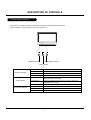
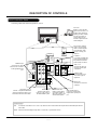
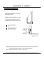
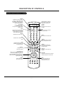
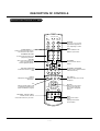
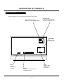
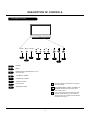
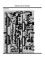
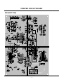
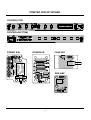
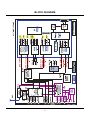
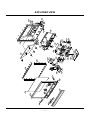
http//www.zenithservice.com
SERVICE MANUAL
Product Type:
Chassis:
Manual Series:
Manual Part #:
Model Line:
Product Year:
Model Series:
LCD Projection TV
MB-042B
2004
CONTENTS
Product Specifications ..................................................4
Description of Controls .................................................5
Adjustment Instructions ...............................................12
Diagrams ...................................................................30
Parts List ...................................................................33
Schematics ....................................................................
Published Oct. 2003
by Technical Publications
LG Electronics USA, Inc.
201 James Record Road,
Huntsville, Alabama 35824-1513
Copyright © 2003 by Zenith Electronics Corporation
Printed in Korea
E44W46LCD
E44W48LCD
PRODUCT SAFETY
IMPORTANT SAFETY NOTICE
This manual was prepared for use only by properly trained audiovisual service
technicians. When servicing this product, under no circumstances should the
original design be modified or altered without permission from Zenith
Electronics Corporation. All components should be replaced only with types
identical to those in the original circuit and their physical location, wiring, and
lead dress must conform to original layout upon completion of repairs. If any
fuse (or Fusible Resistor) in this TV receiver is blown, replace it only with the
factory specified fuse type and rating. When replacing a high wattage resistor
(Oxide Metal Film Resistor, over 1W), keep the resistor 10mm away from PCB.
Always keep wires away from high voltage or high temperature parts.
Special components are also used to prevent shock and fire hazard.
These components are indicated by the letter “x” included in their component
designators and are required to maintain safe performance. No deviations are
allowed without prior approval by Zenith Electronics Corporation. Service work
should be performed only after you are thoroughly familiar with these safety
checks and servicing guidelines.
Circuit diagrams may occasionally differ from the actual circuit used.
This way, implementation of the latest safety and performance improvement
changes into the set is not delayed until the new service literature is printed.
CAUTION: Do not attempt to modify this product in any way.
Never perform customized installations without manufacturer’s
approval.
Unauthorized modifications will not only void the warranty, but may
lead to property damage or user injury.
1. Immediately before handling any semiconductor component or
semiconductor-equipped assembly, drain off any electrostatic charge on the
body by touching a known earth ground. Alternatively, obtain and wear a
commercially available discharging wrist strap device, which should be
removed for potential shock reasons prior to applying power to the unit under
test.
2. After removing an electrical assembly equipped with ES devices, place the
assembly on a conductive surface such as an ESD mat, to prevent
electrostatic charge buildup or exposure of the assembly.
3. Use only a grounded-tip soldering iron to solder or unsolder ES devices.
4. Use only an anti-static solder removal device. Some solder removal devices
not classified as “anti-static” can generate electrical charges sufficient to
damage ES devices.
5. Do not use freon-propelled chemicals. These can generate electrical charge
sufficient to damage ES devices.
6. Do not remove a replacement ES device from its protective package until
immediately before you are ready to install it. (Most replacement ES devices
are packaged with leads electrically shorted together by conductive foam,
aluminum foil, or comparable conductive material.)
7. Immediately before removing the protective material from the leads of a
replacement ES device, touch the protective material to the chassis or circuit
assembly into which the device will be installed.
Caution: Be sure no power is applied to the chassis or circuit, and observe
all other safety precautions.
8. Minimize bodily motions when handling unpackaged replacement ES
devices. (Otherwise, seemingly harmless motion, such as the brushing
together of your clothing or the lifting of your foot from a carpeted floor, can
generate static electricity sufficient to damage an ES device.)
GENERAL GUIDANCE
An lsolation Transformer should always be used during the servicing
of a receiver whose chassis is not isolated from the AC power line. Use a
transformer of adequate power rating to protect against personal injury from
electrical shocks. It will also protect the receiver and its components from being
damaged by accidental shorts of the circuitry that may be inadvertently
introduced during the service operation.
Before returning the receiver to the customer, always perform an AC leakage
current check on the exposed metallic parts of the cabinet, such as antennas,
terminals, etc., to be sure the set is safe to operate
without damage of electrical shock.
LEAKAGE CURRENT COLD CHECK
(ANTENNA COLD CHECK)
With the instrument’s AC plug removed from AC source, connect an electrical
jumper across the two AC plug prongs. Place the AC switch in the on position,
connect one lead of ohm-meter to the AC plug prongs tied together, and touch
other ohm-meter lead in turn to each exposed metallic parts such as antenna
terminals, phone jacks, etc. If the exposed metallic part has a return path to the
chassis, the measured resistance should be between 1MΩ and 5.2MΩ. When
the exposed metal has no return path to the chassis the reading must be
infinite. Any other abnormality that exists must be corrected before
the receiver is returned to the customer.
REGULATORY INFORMATION
This equipment has been tested and found to comply with the limits for a Class
B digital device, pursuant to Part 15 of the FCC Rules.
These limits are designed to provide reasonable protection against harmful
interference when the equipment is operated in a residential installation. This
equipment generates, uses and can radiate radio frequency energy and, if not
installed and used in accordance with the instruction manual, may cause
harmful interference to radio communications. However, there is no guarantee
that interference will not occur in a particular installation. If this equipment does
cause harmful interference to radio or television reception, which can be
determined by turning the equipment off and on, the user is encouraged to try
to correct the interference by one or more of the following measures: Reorient
or relocate the receiving antenna; Increase the separation between the
equipment and receiver; Connect the equipment into an outlet on a circuit
different from that to which the receiver is connected; Consult the dealer or an
experienced radio/TV technician for help.
The responsible party for this device’s compliance is:
Zenith Electronics Corporation
201 James Record Road
Huntsville, AL 35824, USA
Digital TV Hotline: 1-800-243-0000
ELECTROSTATICALLY SENSITIVE DEVICES
Some semiconductor (solid-state) devices can be damaged easily by static
electricity. Such components commonly are called Electrostatically Sensitive
(ES) Devices. Examples of typical ES devices are integrated circuits and some
field-effect transistors and semiconductor “chip” components. The following
techniques should be used to help reduce the incidence of component damage
caused by static electricity.
- 2 -
TABLE OF CONTENTS
SPECIFICATIONS.................................................................4
DESCRIPTION OF CONTROLS ...........................................5
ADJUSTMENT INSTRUCTION...........................................12
PRINTED CIRCUIT BOARDS .............................................18
BLOCK DIAGRAM...............................................................30
EXPLODED VIEW...............................................................32
EXPLODED VIEW PARTS LIST .........................................33
REPLACEMENT PARTS LIST ............................................34
SCHEMATIC DIAGRAM..........................................................
- 3 -
SPECIFICATIONS
Product Specifications
Model
Horizontal Size (Inches)
Height (Inches)
Depth (Inches)
Weight (lbs.)
39.2
29.2
14.4
50.7
Power Requirement
AC 120V, 60Hz
Television System
American TV Standard, NTSC, ATSC with STB
Television Channels
VHF: 2 - 13
UHF: 14 - 69
CATV: 1 - 125
Power Consumption (W)
220W
Antenna
75 ohm External Terminal for VHF/UHF
Audio Output (W)
12W x 2
Supplied Accessories
Remote control, 2 size AA batteries, 2 filters.
External Input/Output Ports
A/V input (3 set)
A/V output (1 set)
S-Video input (2)
Component input (2 set)
RGB input (1)
DVI input (1)
RGB/DVI audio input (1 set)
Variable audio output (1 set)
Audio center mode input (1)
Calibration port (1)
Design and specifications are subject to change without prior notice.
- 4 -
DESCRIPTION OF CONTROLS
Function Status Indicators
Lamp indicator, operation indicator, and temperature indicator located below the front panel
controls, reveal the operating status of the LCD projection TV.
Operation Indicator
Temperature Indicator
Lamp Indicator
Operation Indicator
Lamp Indicator
Temperature Indicator
Off
Red
Green
Orange (flashing)
Orange
Red (flashing)
Green (flashing)
Orange
Red
Red (flashing)
Power cord is not connected.
Power Cord is connected, TV is in standby mode.
TV turns on.
Preparing operation in standby mode.
Projection lamp is reaching the end of its life and needs to
be replaced with a new lamp.
There is a problem with the lamp or around it. Contact an
authorized service center.
The lamp cover is not closed.
The projection TV is overheating.
The projection TV shut down due to overheating.
The projection TV shut down, check the cooling fan.
- 5 -
DESCRIPTION OF CONTROLS
Rear Connections Panel
Connecting cables and external equipment to your TV.
Fan Cover
Replace or clean the filter
to prevent a dust every 1~3
months. When cleaning or
replacing the filter, certainly
turn the main switch off.
The dust filter must be
washed in tepid water with
netural detergent.
RF Connector: Antenna
Used to connect analog
cable or antenna signals
to the television, either
directly or through your
cable box.
ANT IN
+75 Ω
RGB INPUT
PC/DTV
(XGA/
480p/
720p/
1080i)
COMPONENT
UPGRADE PORT
INPUT2 INPUT1
RGB/DVI Input
Connect the TV output
connector from a PC/DTV
to the appropriate input
port.
S-VIDEO In
A connection available with
some high-end equipment
that provides even better
picture quality for Video 2.
S-VIDEO
Y
RGB/DVI INPUT
MONITOR
OUT
VIDEO
INPUT 2
VIDEO
INPUT 1
(L)
VIDEO
AUDIO
(R)
PB
(L)
MONO
PR
PC/DTV
(XGA/
480p/
720p/
1080i)
VARIABLE
AUDIO OUT
(L)
DVI INPUT
AUDIO
CENTER
MODE IN
AUDIO
(R)
AUDIO
(R)
Left/Right Audio
Used for stereo sound
from various types of
equipment.
(L)
AUDIO
Monitor Out
Connects to a second TV
or Monitor.
(R)
DTV/DVD
(480i/480p/720p/1080i)
Component Input 1-2
Connect a component video/audio
device to these jacks. Refer to your
DVD manual for further information.
Video 1 or 2
Connects the video signals from various types
of equipment.
RGB/DVI Input
Used for audio connections from a PC source or
HD-STB Satellite system.
Variable Audio Out
Used to connect either
an external amplifier, or
add a sub-woofer to your
surround sound system.
Audio Center Mode In
Connect to external Dolby
Digital Center “preamp output.”
Mini glossary
JACK
A connection on the back of a TV, VCR, or any other A/V device. This includes the RF jack and the Audio/Video jacks that are
color-coded.
SIGNAL Picture and sound traveling through cable, or over the air, to your television screen.
- 6 -
DESCRIPTION OF CONTROLS
Side Connection Panel
There are four jacks on the left side on your projection TV
that make connecting Audio/Video devices like video games
and camcorders very simple.
The jacks are like those found on the back jack connection
panel. This means that most equipment that connects to
those types of jacks on the rear jackpack, may be connected to the side connection panel.
To use the side jacks as the signal source, select them
using Main Input menu as described on page 25. They will
be named “Side Video” in the Main Input menu.
If you input both Side Video and
S-Video, only the S-Video will
work.
If you’re connecting a video game
device, make sure to change the
picture settings with the EZ
Picture option in the Video menu.
Side A/V Panel
Left/Right Audio
Used for stereo
sound from various
types of equipment.
Video
Connects the video
signals from any
piece of equipment.
(R)
AUDIO
(L)/
MONO
VIDEO
S-VIDEO
SIDE VIDEO
S-Video
A connection available on
some very high-end equipment that provides better
picture quality than video
input.
Mini glossary
A/V CABLESAudio/Video cables. Three cable connector—Right audio (red), Left audio (white), and Video (yellow). A/V cables are used
for stereo playback of videocassettes and for higher quality picture and sound from other A/V devices.
A/V DEVICE Any device that produces video or sound (VCR, DVD, cable box, or television).
- 7 -
DESCRIPTION OF CONTROLS
Remote Control Functions in TV Mode
MODE
Selects the remote operating
mode: TV, VCR, Cable, DVD
and Satellite. Select other operating modes, for the remote to
control external devices.
TV/VIDEO
Selects: Analog, Video1,
Video2, Side video,
Component1-2, RGB, and DVI
input sources.
SIDE
Selects the side video signal if
a device, such as a camcorder
or game player, is connected
to the side video input jack.
MUTE
Switches the sound on or off
SAP
Selects: Mono, Stereo, and
SAP.
INDICATOR LIGHTS
VCR CABLE DVD SAT
TV
MODE
LIGHT
POWER
TV/VIDEO
SIDE
DVI
COMP1
COMP2
RGB
1
2
3
4
5
6
7
8
9
ENTER
0
FLASHBK
Show active remote mode
every time any button is
pressed.
LIGHT
Illuminates the remote control keys.
DVI
SURF
MUTE
Selects: DVI-DTV and DVIPC input sources.
SURF
Scrolls the Surf channel list.
VIDEO
Adjusts the factory preset picture according to the room.
PIP
Toggles between PIP, POP
(Picture-out-of-Picture) and
Twin picture mode.
VIDEO
SAP
VOL
PIP
CH
SWAP
PIPCH- PIPCH+ SWAP
PIPCHChanges to next
lower PIP channel
Switches the picture from
PIP, POP, or twin picture to
the main screen.
PIPCH+
RATIO
CC
FREEZE PIP INPUT
Changes to next higher PIP
channel.
THUMBSTICK
Allows you to navigate the on-screen
menus and to adjust the system settings and preferences, by moving to an
D
option withF E
G and selecting the highlighted option with .
FREEZE
Captures and freezes the currentlyviewed main picture in PIP mode.
MENU
EXIT
EXIT
MENU
Brings up the main
menu to the screen.
PLAY PAUSE STOP RECORD
REW
FF
SKIP
- 8 -
Clears all on-screen displays and returns to TV
viewing from any menu.
DESCRIPTION OF CONTROLS
Remote Control Functions in TV Mode
VCR CABLE DVD SAT
TV
MODE
LIGHT
POWER
TV/VIDEO
SIDE
DVI
COMP1
COMP2
RGB
POWER
RGB
COMPONENT 1, 2
Selects component signal sources,
such as DVD or HD receiver.
1
2
3
NUMBER KEYPAD
4
5
6
7
8
9
ENTER
0
FLASHBK
For direct channel selection and
programming functions.
Turns your TV or any other
programmed equipment on
or off, depending on mode.
Selects: RGB-DTV and
RGB-PC input sources.
ENTER
When in the menu system and
other on-screen displays,
selects highlighted options.
SURF
MUTE
Increases/decreases the sound
level.
VOL
RATIO
PIP
RATIO
CHANNEL UP/DOWN
CH
PIPCH- PIPCH+ SWAP
CC
FREEZE PIP INPUT
Changes the screen format or
aspect ratio.
Scrolls through available channels
in EZ Scan memory.
PIP INPUT
Selects the input source for the
sub picture.
CC
Selects a closed caption mode
for displaying captioning information if available on program.
Tunes to the last channel
viewed.
VIDEO
SAP
VOLUME UP/DOWN
FLASHBK
ENTER
MENU
EXIT
When in the menu system
and other on-screen displays, selects highlighted
options.
PLAY PAUSE STOP RECORD
RECORD, PAUSE, REW,
FFWD, PLAY, STOP
REW
FF
SKIP
Control the functions on your VCR.
SKIP
- 9 -
Playing CDs: Selects
songs.
Playing DVDs: Selects
movie chapters.
DESCRIPTION OF CONTROLS
On-Screen Displays
This page describes your on-screen display and information banner options.
Main Channel Display
Displays current channel number.
TV 13
MONO
ABC
Channel Label
If a channel label has been
set, then it will appear here.
PIP Display
This display
appears when
PIP is active.
TV 6
AM 3:00
10
Mute
Appears
when sound
is muted.
Volume
Volume level is displayed while
adjusting the sound.
- 10 -
Time
Appears when
pressing the
enter button.
DESCRIPTION OF CONTROLS
Front Panel Controls
POWER
MENU
1
ENTER
3
2
VOL
CH
4
5
1
2
POWER
3
ENTER (Same as ENTER button on your
remote control)
4
5
6
7
VOLUME UP / DOWN
8
Temperature indicator.
6
8
7
MENU
CHANNEL UP / DOWN
Operation indicator.
See menu pages for instructions on using the
on-screen menus.
Lamp indicator.
The POWER, MENU, ENTER, VOLUME, and
CHANNEL buttons work just as they do on
your remote control.
If TV is moved from cold to normal room temperature, condensation may form inside TV,
wait 3 hours the TV to adjust to room temperature before turning it on.
- 11 -
ADJUSTMENT INSTRUCTIONS
1. Application Object
4. LCD Adjustment
This instruction is for the application to the LCD projection
4-1. NRS Adjustment
TV(MB-042B Chassis).
[ When the LCD panel load data on regular pixel using high
speed charge/discharge with sample & holder, the drain width
of TFT gradually decreases and the non-resistance increases,
and comes out regular noise on screen(shows vertical line by
12 pixel)
2. Notes
(1) The power source insulation of this LCD Projection TV is not
charging type and you may not use the transformer for insulation. But you better adjust the set after operating it with insulation transformer between power supply cable and input part of
the set for protecting the adjusting equipment.
(2) The adjustment must be performed under the correct
sequence.
(3) The adjustment must be performed in the circumstance of
25!5°C of temperature and 65!10% of relative humidity if
there is no specific designation.
(4) The input voltage of the receiver must keep 120V, 60Hz in
adjusting.
(5) The set must be operated for 15 minutes preliminary before
adjustment if there is no specific designation.
The preliminary operation must be performed after receiving
100% white pattern, but reception of the moving picture may
also be possible in unavoidable case.
This NRS signal is enforced charge/discharge signal so that
the ON/OFF time of TFT mode quickly before starting active
video signal, H/L level adjustment is possible to each R, G, B.
(1) Required Test Equipments
1)
2)
3)
4)
PC Pattern Generator : 16 Step Gray Pattern
Fixation Stand
Remote Control for Adjustment
Circuit thing Jig for Adjustment(Except Driver Board Assy)
(2) Equipment Composition : Follow Fig. 2
(3) Preparation for Adjustment
1) Connect PC Pattern Generator with adjustment Jig like Fig. 2.
(Except Drive part of a circuit block)
2) Select a PC Pattern Generator, 16 Gray.
(4) Adjustment Sequence
1) Turn on a adjustment Jig.
2) Select a RGB_PC by pressing Input Select button on Remote
Control.
3) Enter to adjustment mode by pressing ADJ button on Remote
Control.
4) Select 1. M62352, then ready to adjust RRefV1, GRevV1 and
BRefV1.
5) Let’s decrease vertical line Noise by using Volume button.
(Input a R, G, B input signal, then adjust it individually)
6) When finishing the adjustment, get out of adjustment mode by
pressing ADJ button.
3. Composition of Adjustment Mode
(1) All adjustment mode are entered by pressing the ADJ key on
the remote control, after adjustment press the ADJ key to
come out.
(2) Composition of adjustment mode: The first screen composition of pressing ADJ key.
EZ ADJUST
1. M62352
2. Position
3. AD9883A-set
4. GAMMA
4-2. VCOM Adjustment
5. Uniformity
(1) Required Test Equipments
6. CONTRAST
1) PC PATTERN GENERATOR : Pattern Generator which can
generate each R,G,B signal and can observe the FLICKER
best(ex: me Character Pattern).
2) (Fig. 2) Equipment composition
3) Remote Control
4) Circuit thing Jig for Adjustment(Except Driver Board Assy of
adjustment model)
7. RGB Alignment
8. System Option
9. Lamp Replace
(Fig. 1) The First Screen of Adjustment Mode
(3) Select menu to adjust(turn to yellow) with using (CH+(D),
CH-(E)) key above screen and press the enter key to adjust
on the wanting menu.
(4) After being inputted for SUB menu, select the SUB menu with
using (CH+(D),CH-(E)) key and adjust the value of adjustment with using the volume +(F),volume - (G) key.
(5) Press the ADJ key to come out after adjustment.
- 12 -
ADJUSTMENT INSTRUCTIONS
(2) Equipment Composition
Equipment to measure
Optics
5-3. Horizontal Position Adjustment
(1) Press ADJ key on the remote control to enter the adjustment
mode.
(2) Select 2. Position.
(3) Select H_Position with channel key in adjust mode.
(4) Adjust data with using the Volume key on the remote control
in order to be left/right symmetry screen. (Three blocks of the
most outer block must be located the most outer block.)
(Refer to Fig. 3)
Adjustment Jig
Circuit thing
for Adjustment
SCREEN
PC
SET
Stand
PC Pattern
Generator
5-4. Vertical Position Adjustment
(1) Select V_Position with channel key in adjust mode.
(2) Change the data to symmetrized upper and down of
screen(refer to Fig. 3) by pressing the Volume key on Remote
Control.
(Fig. 2-1) Using Adjustment of Circuit thing for Adjustment
Equipment to measure
Optics
Adj.
Jig
Adjustment Connector
(Fig. 2-2) TV Set status Adjustment
(3) Preparation for Adjustment
1) Connect the PC Pattern Generator with circuit thing for adjustment(circuit block except driver part) and adjustment Jig.
shown upper Fig. 2.
2) Set the PC Pattern generator with displayable
format(DTV720p, SVGA 60Hz, XGA 60Hz) and turn on it.
(Fig. 3) Adjustment for Horizontal/Vertical Position on Screen
6. Component 2 Offset Adjustment
(4) Adjustment Sequence
1) Turn on the adjustment Jig.
2) Select a RGB_PC by pressing Input Select Key on Remote
Control.
3) Enter to adjustment mode by pressing ADJ button on Remote
Control.
4) Select 1. M62352, then ready to adjust RVCOM, GVCOM and
BVCOM.
5) Let’s decrease flicker by using Volume button.
(Input a R, G, B input signal, then adjust it individually)
6) When finishing the adjustment, get out of adjustment mode by
pressing ADJ button on Remote Control.
6-1. Required Test Equipment
Remote control for adjustment, 802F
6-2. Preparation for Adjustment
(1)
(2)
(3)
(4)
Connect a power source with TV Set and turn TV Set on.
Do heat run for 15 min and over before adjustment.
Receive the Component2.
Receive the 720P and HozTVBar Pattern of 802F.
5. Screen Position Adjustment
(Horizontal/Vertical Position Adjustment)
5-1. Required Test Equipment
HozTVBar Pattern
Remote control for adjustment
5-2. Preparation for Adjustment
6-3. Offset Adjustment
(1) Press ADJ key on the Remote Control to enter the adjustment
mode after more than 10 seconds of receiving the signals.
(2) Press the Enter key in 3. AD9883-set of adjustment item to
adjust automatically.
(3) When the adjustment is completed, enter the adjustment
mode by pressing Enter key after appearing “ Adjustment
Completion(Press the Enter)” OSD.
(1) Connect a power source with TV Set and turn TV Set on.
(2) Do heat run for 15 min and over before adjustment.
(3) Receive the main/sub signal of company through 13CH by
split screen.
(4) Adjust screen ratio to 16:9 by pressing ARC Key.
- 13 -
ADJUSTMENT INSTRUCTIONS
(6) Output the 240, 240, 240(15th data in max white output signal
level) in the VDP Test Pattern, change the 15th RGB Data
value to come out white balance x=283, y=297(D9300K) and
measured step luminance in 5).
(7) Output the 224, 224, 224(14th data in max white output signal
level) in the VDP Test Pattern, change the 14th RGB Data
value to come out white balance x=283, y=297(D9300K) and
measured step luminance in 5).
(8) As shown above, output the VDP Test Pattern signal(208/192/176/160/144/128/112/96/80/64/48/32/16) and
change the RGB Data value of each step to come out white
balance x=283, y=297(D9300K) and measured luminance in
3).
7. Adjustment of White Balance and Gamma
7-1. Required Test Equipments
(1) Illuminometer (name of model : CA-100) 1EA —> Measure
color of projecting screen center
[ CA-110(name of model) is possible to measure White
Balance and Gamma —- leave it 20Cm from screen center
Follow a measurement machine manual to set CA-100 and
CA-110 measurement machine.
(2) Pattern Generator 1EA —> 16 step Gray Pattern, 64 step
Gray Pattern
(3) Set Fixation Stand 1EA
(4) Remote Control 1EA
(5) Circuit thing Jig for adjustment(Except Drive Board Assy of
adjustment model)
--- Programmed Digital Board so that the VDP Test Pattern can
output white signal by 1 level form 0 to 255 level.
7-5. Gamma adjustment manually
This is adjustment(after finish the 3-4) to check whether
Gamma/White Balance adjustment are well adjusted and make
correction manually.
7-2. Equipment Composition
(1) Prepare the PC Pattern Generator which is possible to output
R/G/B of 16 step and 64 step Gray Pattern.
(2) Equipment composition : Follow Fig. 2.
(3) Turn on the Jig for adjustment.
(4) Select the RGB_PC by pressing the input select button on
Remote Control.
(5) Output the 16 Gray Pattern in PC Pattern Generator.
Check it with the naked eye whether Screen Gamma and W/B
is right about each Gray.
If it’s not, press the ADJ button on Remote Control and then
adjust the level data of each step manually in sub menu of 4.
Gamma Manual adjust.
(6) Output the 64 Gray Pattern in PC Pattern Generator.
Check it with the naked eye whether Screen Gamma and W/B
is right about each Gray or whether there is Gamma noise.
If there’s any problem, adjust in 5).
(7) After finishing adjustment, exit adjustment mode by using
ADJ button on Remote Control.
Adjust at the same condition of equipment composition diagram.
7-3. Preparation for Adjustment
Compose the equipment follow Fig. 2 and place the set on the
fixation stand.
(1) Select the VDP Test Pattern signal to R1, G1, B1.
(2) Press the Instart key to select 1. LCD --> 2. 62352 and then
select 5. RVREF, 8. GVREF, 12. BVREF in adjust mode.
(3) Adjust the luminance of CA100 below 0.75Cd. (The adjustment range is 196~202)
(4) Exit adjustment mode by pressing ENTER button on Remote
Control.
(5) Select 3. 7050 RGB Set in adjustment mode.
(6) Check the data 1. RContrast, 8. GContrast, 15. BContrast is
515. Otherwise set the data 515 by using volume button.
7-4. Adjustment Sequence
(1) Output the 255,255,255 signal of VDP Test Pattern, then display the maximum white pattern on screen.
(2) Gamma Adjust Mode is display as below when select 4.
Gamma adjust by selecting ADJ key on R/C.
Gamma Adjust Mode
* 1st Column : 16 Step Level
100
216
387
* 2nd Column : R Adjustment
Data
1
2
3
80
234
453
100
216
411
8. White Uniformity Adjustment
8-1. Required Test Equipments
(1) Uniformity measurement equipment : Equipment which can
measure chromaticity in the whole screen
(2) Set Stand 1EA
(3) Remote Control for Adjustment
(4) Circuit thing Jig for Adjustment(Except Driver Board Assy of
adjustment model)
--- Programmed Digital Board so that the VDP Test Pattern can
output white signal by 1 level form 0 to 255 level.
* 3rd Column : G Adjustment
Data
16
724
RGB 456
740
780
* 4th Column : B Adjustment
Data
8-2. Equipment Composition
Step123
Compose the equipment follow Fig. 2 and place the set on the
fixation stand.
(3) Change the 16 Step RGB Data to select white balance
x=283, y=297(D9300K).
(4) Measure the luminance with changed data.
(5) Set the every Gamma data of 16 step to 2.2 on the basis of
measured luminance data in 3).
(Max luminance *(n1/16)**2.2) — Max luminance : measured
luminance data n1 = every step unit when separating signal
level to 16 step)
8-3. Preparation for Adjustment
- 14 -
(1) Composite the equipment as shown Fig 2, and place the set
on fixation stand.
(2) After inputting company channel 13, adjust color uniformity
like Horizontal/Vertical position adjustment of input signal part
adjustment by using Remote Control for adjustment.
ADJUSTMENT INSTRUCTIONS
(3) After pressing ADJ key on Remote Control for adjustment,
select the adjustment mode 5. Uniformity adj.
Refer to register value and correct register value if need.
1.
2.
3.
4.
5.
6.
<Resister Explanation about uniformity adjustment>
RamCtrl : s/w saving uniformity write order(Do not adjust)
CSHP : Horizontal start point designation ---adjustable
CSVP : Vertical start point designation ---adjustable
CEHP : Horizontal END point designation ---adjustable
CEVP : Vertical END point designation ---adjustable
Mode : uniformity mode select --- adjustable if need
*** 0 : 221point & 3level ---- default value
*** 1 : 221point & 4level
*** 2 : 825point & 3level
*** 3 : 825point & 4level
7. KHH : Upper 2byte of horizontal line correction coefficient -Change according to CSHP, CEHP value.
8. KHL : Upper 2byte of vertical line correction coefficient -Change according to CSHP, CEHP value.
14. RL2L : Lower 9bit of MID1 brightness correction coefficient in
R MID2.
--- Change according to RMID2 and RMID1 value.
15. RL3H : Upper 9bit of MAX brightness correction coefficient in
R MID1.
--- Change according to RMID1 and RMAX value.
(use it while adjusting 4 coefficient)
16. RL3L : Lower 9bit of MAX brightness correction coefficient in
R MID1.
--- Change according to RMID1 and RMAX value.
(use it while adjusting 4 coefficient)
<L Coefficient Calculation Method>
Using 3coefficient Level
Assume that the value of R/G/B MIN, MID2,MID1 is 192, 448,
704.
R/G/B MIN = 192
R/G/B MID2 = 448
R/G/B MID1 = 704
O
** How to calculate KHH, KHL value
LCD panel size = 1280 x 720
Correction Point = 221 point
--> 17 horizontal points x 13 vertical points
(16 horizontal segments x 12 vertical points)
O
L Coefficient(RL1H~BL3L)
--> Calculation method (L1)
L1 coefficient = 1 / (brightness level(MID2) - brightness level(MIN)
L1coeff = 1 / (448-192) = 1 / 256 = 0.00390625
L1coeff(hex) = hex(0.00390625 x 218) = 0 x 0400
H Coefficient(KHH, KHL)
--> Calculation method (CEHP-CSHP=1280, Horizontal
segment value =16)
--> L1H(high 9bit) = b’000000010 L1L(low 9bit) = b’000000000
- calculate L2, L3 same with L1
H coefficient = 1/(number of pixel intervals between setting in the horizontal
direction)
L2 coefficient = 1 / (brightness level(MID1) - brightness level(MID2)
Hcoeff = 1/((1280/16)-1) = 0.012658227
L3 coefficient = 1 / (brightness level(MAX) - brightness level(MID1)
: case of 4 Brightness Level
hex(0.012658227 x 216) = 0 x 033D, Hcoeff(hex) = 0 x 033D + 1 = 0 X 33E
9. KVH : Upper 2byte of vertical line correction coefficient -Change according to CSVP, CEVP value.
10. KVL : Upper 2byte of vertical line correction coefficient -Change according to CSVP, CEVP value.
O
V Coefficient(KVH, KVL)
--> Calculation method (CEVP-CSVP=720, Vertical segment
value =12)
V coefficient = 1/(number of pixel intervals between setting in the horizontal
direction)
Vcoeff = 1/((720/12)-1) = 0.016949152
hex(0.016949152 x 216) = 0 x 0456, Vcoeff(hex) = 0 x 0456 + 1 = 0 X 0457
11. RL1H : Upper 9bit of MID2 brightness correction coefficient in
R MIN.
--- Change according to RMIN and RMID2 value.
12. RL1L : Lower 9bit of MID2 brightness correction coefficient in
R MIN.
--- Change according to RMIN and RMID2 value.
13. RL2H : Upper 9bit of MID1 brightness correction coefficient in
R MID2.
--- Change according to RMID2 and RMID1 value.
17. GL1H : Upper 9bit of MID2 brightness correction coefficient in
G MIN.
--- Change according to GMIN and GMID2 value.
18. GL1L : Lower 9bit of MID2 brightness correction coefficient in
G MIN.
--- Change according to GMIN and GMID2 value.
19. GL2H : Upper 9bit of MID1 brightness correction coefficient in
G MID2.
--- Change according to GMID2 and GMID1 value.
20. GL2L : Lower 9bit of MID1 brightness correction coefficient in
G MID2.
--- Change according to GMID2 and GMID1 value.
21. GL3H : Upper 9bit of MAX brightness correction coefficient in
G MID1.
--- Change according to GMID1 and GMAX value.
(use it while adjusting 4 coefficient)
22. GL3L : Lower 9bit of MAX brightness correction coefficient in
G MID1.
--- Change according to GMID1 and GMAX value.
(use it while adjusting 4 coefficient)
23. BL1H : Upper 9bit of MID2 brightness correction coefficient in
B MIN.
--- Change according to BMIN and BMID2 value.
24. BL1L : Lower 9bit of MID2 brightness correction coefficient in
B MIN.
- 15 -
ADJUSTMENT INSTRUCTIONS
--- Change according to BMIN and BMID2 value.
25. BL2H : Upper 9bit of MID1 brightness correction coefficient in
B MID2.
--- Change according to BMID2 and BMID1 value.
26. BL2L : Lower 9bit of MID1 brightness correction coefficient in
B MID2.
--- Change according to BMID2 and BMID1 value.
27. BL3H : Upper 9bit of MAX brightness correction coefficient in
B MID1.
--- Change according to BMID1 and BMAX value.
(use it while adjusting 4 coefficient)
28. BL3L : Lower 9bit of MAX brightness correction coefficient in
B MID1.
--- Change according to BMID1 and BMAX value.
(use it while adjusting 4 coefficient)
29. RLMIN : Setting up the MINIUM Level of R --- Set under 200
30. RLMID2 : Setting up the MIDDLE 2nd Level of R ---Middle
level when 3coefficient
31. RLMID1 : Setting up the MIDDLE 1st Level of R --- Max level
when 3coefficient
32. RLMAX : Setting up the MAX Level of R
33. GLMIN : Setting up the MINIUM Level of G --- Set under 200
34. GLMID2 : Setting up the MIDDLE 2nd Level of G ---Middle
level when 3coefficient
35. GLMID1 : Setting up the MIDDLE 1st Level of G --- Max level
when 3coefficient
36. GLMAX : Setting up the MAX Level of G
37. BLMIN : Setting up the MINIUM Level of B --- Set under 200
38. BLMID2 : Setting up the MIDDLE 2nd Level of B --- Middle
level when 3coefficient
39. BLMID1 : Setting up the MIDDLE 1st Level of B --- Max level
when 3coefficient
40. BLMAX : Setting up the MAX Level of B
41. HVSCAN : Setting up the scan direction while adjusting uniformity - Do not adjust
42. TestMode : uniformity adjustment test - Do not adjust
At this time, make sure that deviation is +5~-5% and standard
is color coordinate of center.
(3) Output the VDP TEST PATTERN signal correspond to the
MID value.
Read the white coordinates and communicate 3 line with
ET7050 IC through measurement equipment of optics.
Adjust screen coordinates data to adjust the color uniformity of
mid point.
At this time, make sure that deviation is +5~-5% and standard
is color coordinate of center.
(4) Output the VDP TEST PATTERN signal correspond to the
MIN value.
Read the white coordinate and communicate with ET7050 IC
through measurement equipment of optics.
Adjust screen coordinates data to adjust the color uniformity of
miner point.
At this time, make sure that deviation is +5~-5% and standard
is color coordinate of center.
(5) White the miner, middle, maximum data for each point to confront to each MICOM address.
9. Brightness Adjustment of Main/Sub
Screen
8-4. Adjustment Sequence
(1) Adjust the screen coordinates as shown below.
0
1 2 3 ............xx..........15 16
1
Operate this adjustment when the brightness of Main/Sub screen
is different.
(1) Receive signal(RF 06Ch.) on the Main/Sub screen in the twin
picture.
(2) Confirms picture probably is the normal.
(3) Check the “US06CH” with naked eyes in 06Ch. pattern and if
there is difference, adjust like this.
- The field and the letters are distinguished.
(4) Adjusting Main screen
1) Select the 6. CONTRAST by pressing “ADJ” key on the
remote control for adjustment.
2) Select the Contrast(m) of adjustment item using CH +/- key
and revises using VOL +/- key.
(5) Adjusting Sub screen
1) Select the 6. CONTRAST by pressing “ADJ” key on the
remote control for adjustment.
2) Select the Contrast(s) of adjustment item using CH +/- key
and revises using VOL +/- key.
.
yy
.
* Ask for repairs when the data value is changed over !2.
(Initial Value: 32)
11
12
(Fig. 4) Screen division diagram for uniformity adjustment
(2) Output the VDP TEST PATTERN signal correspond to the
Max value.
Read the white coordinates and communicate 3 line with
ET7050 IC through measurement equipment of optics.
Adjust screen coordinates data to adjust the color uniformity of
max point.
- 16 -
ADJUSTMENT INSTRUCTIONS
10. EDID Data Input
10-1. Required Test Equipment
(1) Jig for adjusting PC, DDC.
(PC serial to D-sub. Connection equipment)
(2) S/W for writing DDC (EDID data write & read)
(3) D-sub terminal
10-2. Setting of Devices
LCD PJTV
SET
(Fig. 5) Deviating Red Pixel, collectively(before adjusting)
10-3. Preparation for Adjustment
(1) Set devices as above and turn the PC, jig on.
(2) Put the S/W for writing DDC (EDID data write & read) into
operation. (Operated in DOS mode.)
10-4. Sequence of Adjustment
(1) Put the SET on the table and turn the power on.
(2) Input the product code, production week/year, serial number
(if it is not input, write “01”) to the S/W for writing DDC.
(3) Put the EDID write instruction into operation.
11. Check and adjustment RGB Alignment
(Fig. 6) After adjusting RGB Align(normal screen)
11-1. Required Test Equipment
Remote control for adjustment
11-2. Preparation for Adjustment
(1) Connect power source with TV Set and turn TV Set on.
(2) Before adjusting, Heat Run more than 15 minutes.
11-3. Check and adjustment RGB Alignment
(1) After pressing EYE key, enter the (Fig. 5) pattern.
(2) Check the RGB Align
(3) When fitting RGB Align, adjustment is completed.
(4) When deviating RGB Align, select the 7. H-Position by pressing “ADJ” key on the Remote Control for Adjustment.
Change the Channel key to select H POS R, H POS G, H
POS B and fit color.
- 17 -
PRINTED CIRCUIT BOARD
MAIN(TOP)
- 18 -
PRINTED CIRCUIT BOARD
MAIN(BOTTOM)
- 19 -
PRINTED CIRCUIT BOARD
TUNER(TOP)
- 20 -
PRINTED CIRCUIT BOARD
TUNER(BOTTOM)
- 21 -
PRINTED CIRCUIT BOARD
DRIVER(TOP)
- 22 -
PRINTED CIRCUIT BOARD
DRIVER(BOTTOM)
- 23 -
PRINTED CIRCUIT BOARD
DIGITAL(TOP)
- 24 -
PRINTED CIRCUIT BOARD
DIGITAL(BOTTOM)
- 25 -
PRINTED CIRCUIT BOARD
SMPS
AC INPUT
- 26 -
PRINTED CIRCUIT BOARD
AUDIO(TOP)
AUDIO(BOTTOM)
- 27 -
PRINTED CIRCUIT BOARD
CRM(TOP)
CRM(BOTTOM)
SIDE A/V
- 28 -
PRINTED CIRCUIT BOARD
CONTROL(TOP)
CONTROL(BOTTOM)
POWER S/W
INTERFACE
CASE DET
PRE-AMP
- 29 -
BLOCK DIAGRAM
- 30 -
NOTES
- 31 -
310
650
302
300
305
301
120
330
121
- 32 501
520
540
560
303
571
570
550
304
601
600
572
503
580
581
430
174
720
700
630
640
530
681
680
611
610
612
620
400
410
670
402
401
EXPLODED VIEW
EXPLODED VIEW PARTS LIST
No.
Description
Part No.
120
6400WESC01A
SPEAKER,WOOFER C080P23K1450 ESTEC WOOFER 8OHM 15/25W 84DB 80 NON
121
6400DESA01A
SPEAKER,TWEETER D016D01K1450 8HMOHM 15/25W 85DB 50 NON
174
6410VUH004A
POWER CORD,UL/CSA3000MM 3P HUG BLACK VOLEX CSA 3000MM
300
3090V00556A
CABINET,DN-44SZ80L LCD PJT FRONT
3090V00590A
CABINET,DN-44SZ80L LCD PJT LGERS
4810V00978A
BRACKET,SPEAKER DN-44SZ80L NON ABS ZENITH
4811V00099J
BRACKET ASSEMBLY,GRILLE *E44W48LCD
3520V00436A
INDICATOR,LED RU-44SZ80L PMMA 3 PHY NON
3520V00401A
INDICATOR,LED *E44W48LCD
303
4980V00A29A
SUPPORTER,SCREEN AL BAR(U/L)
304
4980V00A29B
SUPPORTER,SCREEN AL BAR(R/L)
305
3351V00020A
SCREEN ASSEMBLY,SHIINSUNG LGE WLF DN-44SZ80L 991*564*3.4 .
3351V00020B
SCREEN ASSEMBLY LGERS
310
5020V00903A
BUTTON,CONTROL DN-44SZ80L ABS 7KEY XCANVAS
330
5020V00904C
BUTTON,POWER RU-44SZ81L ABS, AF-303S 1KEY ZENITH
5020V00904B
BUTTON,POWER *E44W48LCD
3808V00455A
BACK COVER,DN-44SZ80L NB-042A
3808V00483A
BACK COVER,RU-44SZ80L LGERS
401
3550V00424A
COVER,NON DN-44SZ80L ABS POWER CODE
402
3550V00423C
COVER,LAMP RU-44SZ80L HIPS 40AF NON
410
3550V00425A
COVER,NON DN-44SZ80L ABS DUST
3550V00550A
COVER ASSY RU-44SZ81L(LGERS)
430
5018V00039F
MIRROR
501
3210V00165B
FRAME,ABS, AF-303S RN-48SZ40H MAIN CHASSIS
503
4811V00125D
BRACKET ASSEMBLY,REAR AV RU-44SZ80L MB042B TERMINAL BOARD
520
6871VMMR46H
PCB ASSEMBLY,MAIN MB-042A RU-44SZ81L
6871VMMR46N
PCB ASSEMBLY,MAIN *E44W48LCD
530
6871VPMA46A
PCB ASSEMBLY,POWER SMPS NB-042A RU-44SZ80L MI
540
6871VSME68A
PCB ASSEMBLY,SUB TUNER MB042A RU-44SZ80L
550
6871VSMX04H
PCB ASSEMBLY,SUB DIGITAL MB042B RU-44SZ81L
6871VSMX04R
PCB ASSEMBLY,SUB DIGITAL *E44W48LCD
560
6871VSME84A
PCB ASSEMBLY,SUB CRM MB042A RU-44SZ80L
570
6871VSML01B
PCB ASSEMBLY,SUB MB042A DIRVER 80H
571
4814V00444B
SHIELD,CASE DN-44SZ80L NON EGI EMI CASE(0.7W LCD)
572
4814V00459G
SHIELD ASSY,DN-44SZ80L NB042A NON COVER DIRIVER BOARD
580
5900V11001F
FAN,DC B1232S06B2 DONGYANG 120*120*32 6V 950RPM DC5-8V L=850MM
581
4810V00983B
BRACKET,NON DN-44SZ80L NON NON IN TAKE SIRROCO FAN
600
3141VSN916C
CHASSIS ASSEMBLY,ENGINE NB042A RU-44SZ80L OPTICAL ENGINE ASSY
601
4980V00A20E
SUPPORTER,ENGINE EGI EGI 0.7W ENGINE 44SZ80
610
6912V00006C
LAMP,HIGH PRESSURE MECURY UHP 100W 1.0 PH P22 PHILIPS 100V 1A
611
4810V00710A
BRACKET,NON RN-48SZ40 NON NON LAMP
612
4980V00620E
SUPPORTER,NON AL DN-44SZ80L LAMP COVER
620
5900V09006B
FAN,DC G923206B2-RS DONGYANG 92*92*32 6V 1300RPM DC5-8V L=850MM
630
6871VSN221E
PCB ASSEMBLY,SUB P/AMP NB042A DN-44SZ80L
640
6913V00002C
BALLAST,EUC100 P/11 PHILIPS 100W POWERPACK BALLAST FOR LCD
650
6871VSME75A
PCB ASSEMBLY,SUB CONT MB042A 80L CONTROL
670
6871VSME03D
PCB ASSEMBLY,SUB MB042A 80L CASE DET
680
6871VSN220B
PCB ASSEMBLY,SUB MB042A SIDE AV DN-44SZ80L
681
3500V00061J
BOARD,AV RU-44SZ80L NB042A ZENITH
700
6871VSME82A
PCB ASSEMBLY,SUB INTER MB042A DN-44SZ80L
720
6871VPMA47A
PCB ASSEMBLY,POWER SMPS NB-042A RU-44SZ80L AC INPUT MI
301
302
400
- 33 -
REPLACEMENT PARTS LIST
For Capacitor & Resistors, the
charactors at 2nd and 3rd digit
in the P/No. means as follows;
LOCA. NO
CC, CX, CK, CN : Ceramic
CQ : Polyestor
CE : Electrolytic
PART NO
RD : Carbon Film
RS : Metal Oxide Film
RN : Metal Film
RF : Fusible
DESCRIPTION
IC
IC1
0IZZVC0124A
M37151EFFP 42P MICOM
IC100
0IPH741400E
74HC14D 14SOP
IC100
0IPMGON013B
IC1000
0IMI623200B
M62320FP 16P
IC1001
0IMI623200B
M62320FP 16P
IC1001
0ICTMMI057A
M37151EFFP 42P MICOM
IC1002
0IKE704200J
KIA7042AF SOT89 TP 4.2V
IC1003
0IAL242561B
AT24C256W10SI2.7V 8P
IC1005
0IMCRTH003A
THC63LVD104A 64P
IC1007
0IPRPSH001A
PQ20WZ1U 5P SC63
IC1008
0IMI623520B
IC101
0IMCRKE006A
KIA278R05PI TO220IS,4P
IC1010
0IMCRSJ001A
SC1565IST1.8 3P SOT223
IC1011
0IPRPFA006A
RC1117S33T SOT223
IC1012
0IMCRSB012A
L3E07070K0A 324P VIDEO SIGNAL
IC1013
0IMO324000C
LM324D SO14 TP OP AMP
IC1014
0IMO324000C
LM324D SO14 TP OP AMP
IC1019
0IPRPFA006A
RC1117S33T SOT223 R/TP 3.3VOLT
IC102
0IMCRMI070A
M306V7MGFP 100P
“
0IMCRMI070B
M306V7FJFP 100P *E44W48LCD
IC102
0IKE780900M
KIA7809API TO220 ST 3P 9V
IC1020
0IMCRSB014A
L3E06110D0A TQFP 100P VIDEO SIGNAL
IC1021
0IPRPFA006A
RC1117S33T SOT223 R/TP 3.3VOLT
IC1022
0IMCRSB014A
L3E06110D0A TQFP 100P VIDEO SIGNAL
IC1023
0IPRPFA006A
RC1117S33T SOT223 R/TP 3.3VOLT
IC1024
0IMCRSB014A
L3E06110D0A TQFP 100P VIDEO SIGNAL
IC103
0IMP242560A
24LC256I/SM 8P
IC104
0IKE702700D
KIA7027AF 3, SOT89 TP RESET IC 2.7V
IC105
0IMCRSG010A
ST3232CDR SOP16 R/TP RS232
IC106
0IMCRTH002A
THC63LVD103 64P
IC107
0IMCRET002B
EL2250CST7 8P R/TP OP AMP
IC1106
0IPRPFA006A
IC1200
IC1201
IC2
IC200
IC3
IC300
IC301
IC302
IC304
IC305
IC306
IC307
IC4
IC404
IC405
0IPMGKE030A
0IMCRSO025A
0IMCRKE019A
0ISO206900A
0IMCRKE018A
0IIT323000E
0IFA741230A
0IMCRXL003A
0IPH827150A
0IMMRAL014B
0IMCRAD002A
0IMCRS5003A
0IFA754207A
0IMCRKE006A
0IMCRKE006B
MC34063ADR2G SO8P DCDC
M62352GP 20P SSOP TP 8BITS
RC1117S33T SOT223 R/TP 3.3VOLT
KIA78R05F 5PIN DPAK R/TP 1A,5V
CXA2181Q SONY 48P VIDEO
KIA78R33API KEC 4P TO220 ST 3.3V 1A
CXA2069Q QFP64 BK I2C BUS AV S/W
KIA78R05API KEC 4P TO220 ST 5V 1A
VPC3230D C5 80P QFP TRAY VIDEO
DM74LS123MX 16SOP
XC95144XL10TQ100C 3.3V 100P
P82B715T 8SOP
AT24C02N10SI2.7 8P
AD9883AKST110 80P DIGITAL BOARD
SIL169CT100 100P
KA75420ZTA 3P,TO92 TP 4.2V
KIA278R05PI TO220IS,4P
KIA278R33PI TO220IS 4P
RUN DATE : 2004.5.11
LOCA. NO
PART NO
DESCRIPTION
IC406
0IMCRKE006B
KIA278R33PI TO220IS 4P
IC407
0IPMGKE045A
KIA278R25PI 2.5V 2A KEC TO220IS 4P
IC409
0IMCRKE003B
KIA78R12API KEC 4P TO220IS
IC5
0IMCRAL006A
AT24C16AN10SI2.7 8P SOIC R/TP EEPROM
IC500
0ICTMLG003C
LGDT1502M 304P READY2 AMKOR
IC501
0IMMRHY033A
HY57V643220C(L)T6 86P 64M
IC502
0ITI740000Q
SN74LVC00AD 14SOP R/TP LOGIC DTV
IC503
0ICTMLG013A
LGDT1901A LG IC 24P SSOP TRAY DPLL
IC504
0IMMRHY033A
HY57V643220C(L)T6 86P 64M
IC600
0IMCRMN014A
MSP3440G QA B8 V3 80 SOUND IC
IC601
0ISS455880A
KA4558D 8SOP OP AMP
IC602
0IFA754207A
KA75420ZTA 3P,TO92 TP 4.2V
IC701
0IMCRKE006B
KIA278R33PI KEC TO220IS 4P ST 3.3V
IC702
0ISS416162C
K4S161622ETC80 50TSOP
IC702
0IMCRKE006B
KIA278R33PI KEC TO220IS 4P
IC703
0IPMGKE045A
KIA278R25PI 2.5V 2A KEC TO220IS 4P
IC703
0IMCRNE045A
UPD64011AGM8EDA 160P
IC706
0ISA428200A
IC809
0IPMGSG018C
LD1086DT15TR 2P DPAK R/TP 1.5V 1.5A
IC810
0IMCRSK004A
SMAE1017 3P TO220 ST PFC&QRC COMBO
IC830
0ISH817300B
PC817XF3 4D PHOTO COUPLER
IC850
0ISH302122A
PQ30RV21 TO220
IC851
0IMCRFA007A
KA431Z 3DIP,TO92
IC870
0IMCRFA007A
KA431Z 3DIP,TO92
IC900
0ICTMLG018A
LGDT4410 LG IC 176P
LA4282 12S 2CHX10W AUDIO AMP
TRANSISTOR
Q1
0TR387500AA
CHIP 2SC3875S(ALY) KEC
Q100
0TR830009BA
BSS83
Q100
0TR387500AA
CHIP 2SC3875S(ALY) KEC
Q1000
0TR387500AA
CHIP 2SC3875S(ALY) KEC
Q1001
0TR387500AA
CHIP 2SC3875S(ALY) KEC
Q1002
0TR387500AA
CHIP 2SC3875S(ALY) KEC
Q1003
0TR387500AA
CHIP 2SC3875S(ALY) KEC
Q1004
0TR387500AA
CHIP 2SC3875S(ALY) KEC
Q1005
0TR387500AA
CHIP 2SC3875S(ALY) KEC
Q101
0TR830009BA
BSS83
Q102
0TR102009AG
CHIP KRC102S KEC TP SOT23
Q103
0TR387500AA
CHIP 2SC3875S(ALY) KEC
Q104
0TR387500AA
CHIP 2SC3875S(ALY) KEC
Q105
0TR150400BA
CHIP 2SA1504S(ASY) KEC
Q107
0TR387500AA
CHIP 2SC3875S(ALY) KEC
Q1201
0TR387500AA
CHIP 2SC3875S(ALY) KEC
Q1202
0TR387500AA
CHIP 2SC3875S(ALY) KEC
Q1203
0TR387500AA
CHIP 2SC3875S(ALY) KEC
Q1204
0TR387500AA
CHIP 2SC3875S(ALY) KEC
Q1205
0TR387500AA
CHIP 2SC3875S(ALY) KEC
Q1206
0TR387500AA
CHIP 2SC3875S(ALY) KEC
- 34 -
REPLACEMENT PARTS LIST
LOCA. NO
PART NO
DESCRIPTION
LOCA. NO
PART NO
DESCRIPTION
Q1208
0TR150400BA
CHIP 2SA1504S(ASY) KEC
D1
0DD184009AA
KDS184S CHIP 85V 300MA
Q1209
0TR387500AA
CHIP 2SC3875S(ALY) KEC
D100
0DRSE00038A
SDC15 TVS SOT23 12.8V
Q1210
0TR150400BA
CHIP 2SA1504S(ASY) KEC
D100
0DRDI00148A
B140A DIODES R/TP SMA 40V
Q1211
0TR387500AA
CHIP 2SC3875S(ALY) KEC
D102
0DR050008AA
SD05.TC SOD323 5V 5A 15A
Q1213
0TR387500AA
CHIP 2SC3875S(ALY) KEC
D103
0DR050008AA
SD05.TC SOD323 5V 5A 15A
Q1218
0TR150400BA
CHIP 2SA1504S(ASY) KEC
D104
0DR050008AA
SD05.TC SOD323 5V 5A 15A
Q1219
0TR387500AA
CHIP 2SC3875S(ALY) KEC
D105
0DRSE00038A
SDC15 TVS SOT23 12.8V
Q1222
0TR387500AA
CHIP 2SC3875S(ALY) KEC
D106
0DR050008AA
SD05.TC SOD323 5V 5A 15A
Q1223
0TR387500AA
CHIP 2SC3875S(ALY) KEC
D2
0DLLT0260AA
LED,LTL30EWJ
Q1224
0TR387500AA
CHIP 2SC3875S(ALY) KEC
D201
0DD414809ED
1N4148 TP GRANDE
Q1225
0TR387500AA
CHIP 2SC3875S(ALY) KEC
D3
0DLLT0260AA
LED,LTL30EWJ
Q200
0TR387500AA
CHIP 2SC3875S(ALY) KEC
D3
0DD226239AA
CHIP KDS226 SOT23
Q201
0TR387500AA
CHIP 2SC3875S(ALY) KEC
D300
0DD184009AA
KDS184S CHIP 85V 300MA KEC TP
Q202
0TR387500AA
CHIP 2SC3875S(ALY) KEC
D4
0DD184009AA
KDS184S CHIP 85V 300MA KEC TP
Q203
0TR387500AA
CHIP 2SC3875S(ALY) KEC
D5
0DD184009AA
KDS184S CHIP 85V 300MA KEC TP
Q204
0TR387500AA
CHIP 2SC3875S(ALY) KEC
D6
0DD184009AA
KDS184S CHIP 85V 300MA KEC TP
Q205
0TR387500AA
CHIP 2SC3875S(ALY) KEC
D700
0DS113379BA
1SS133 T72 DO34 90V
Q206
0TR102008AA
KRA102S R/TP KEC SOT23 CHIP TR
D701
0DS113379BA
1SS133 T72 DO34 90V
Q207
0TR387500AA
CHIP 2SC3875S(ALY) KEC
D702
0DS113379BA
1SS133 T72 DO34 90V
Q208
0TR387500AA
CHIP 2SC3875S(ALY) KEC
D703
0DS113379BA
1SS133 T72 DO34 90V
Q209
0TR387500AA
CHIP 2SC3875S(ALY) KEC
D704
0DS113379BA
1SS133 T72 DO34 90V
Q210
0TR387500AA
CHIP 2SC3875S(ALY) KEC
D706
0DS113379BA
1SS133 T72 DO34 90V
Q211
0TR387500AA
CHIP 2SC3875S(ALY) KEC
D707
0DS113379BA
1SS133 T72 DO34 90V
Q212
0TR387500AA
CHIP 2SC3875S(ALY) KEC
D708
0DS113379BA
1SS133 T72 DO34 90V
Q302
0TR387500AA
CHIP 2SC3875S(ALY) KEC
D709
0DS113379BA
1SS133 T72 DO34 90V
Q305
0TR387500AA
CHIP 2SC3875S(ALY) KEC
D710
0DD184009AA
KDS184S CHIP 85V 300MA KEC TP
Q306
0TR387500AA
CHIP 2SC3875S(ALY) KEC
D711
0DD184009AA
KDS184S CHIP 85V 300MA KEC TP
Q307
0TR387500AA
CHIP 2SC3875S(ALY) KEC
D712
0DD184009AA
KDS184S CHIP 85V 300MA KEC TP
Q308
0TR830009BA
BSS83
D801
0DD606000AA
RBV606 600V 6A 150A NA 10UA
Q309
0TR830009BA
BSS83
D831
0DD100009AU
EU1AV(1)
Q310
0TR387500AA
CHIP 2SC3875S(ALY) KEC
D832
0DD100009AU
EU1AV(1)
Q311
0TR387500AA
CHIP 2SC3875S(ALY) KEC
D834
0DR010009AA
EG01C 1000V 0.5A 10A 100NSEC 50UA
Q600
0TR387500AA
CHIP 2SC3875S(ALY) KEC
D835
0DD414809ED
1N4148 TP GRANDE
Q601
0TR387500AA
CHIP 2SC3875S(ALY) KEC
D840
0DD414809ED
1N4148 TP GRANDE
Q602
0TR387500AA
CHIP 2SC3875S(ALY) KEC
D851
0DD120000BB
FMLG12S
Q603
0TR387500AA
CHIP 2SC3875S(ALY) KEC
D861
0DD120000BB
FMLG12S
Q604
0TR387500AA
CHIP 2SC3875S(ALY) KEC
D881
0DD120000BB
FMLG12S
Q701
0TR150400BA
CHIP 2SA1504S(ASY) KEC
D891
0DRSA00170A
FMLG14S TO220 400V
Q703
0TR150400BA
CHIP 2SA1504S(ASY) KEC
Q801
0DR360000AA
FMG36S 2.2V 100NSEC 1.0MA
Q704
0TR150400BA
CHIP 2SA1504S(ASY) KEC
ZD01
0DR050008AA
SD05.TC SOD323 5V 5A 15A
Q801
0TFSG10004A
STW20NK50Z SGST(STM)
ZD1
0DZ620009BB
ZENERS,MTZJ6.2B
Q830
0TFSG10003A
STW8NK80Z SGST(STM)
ZD10
0DZ620009BB
ZENERS,MTZJ6.2B
Q832
0TR945009AA
KSC945CY TO92 50V 150MA
ZD2
0DZ620009BB
ZENERS,MTZJ6.2B
Q832
0TR437000BA
KTC4370AY TO220IS KEC
ZD201
0DZ560009CF
ZENERS,MTZJ5.6B
Q840
0TR322709AA
KTC3227Y,TP(KTC1627A),KEC
ZD202
0DZ560009CF
ZENERS,MTZJ5.6B
Q852
0TR945009AA
KSC945CY TO92 50V 150MA
ZD203
0DZ560009CF
ZENERS,MTZJ5.6B
Q871
0TR102409AB
KTA1024Y (KTA949) TP KEC
ZD204
0DZ560009CF
ZENERS,MTZJ5.6B
Q872
0TR322709AA
KTC3227Y,TP(KTC1627A),KEC
ZD3
0DZ620009BB
ZENERS,MTZJ6.2B
ZD4
0DZ620009BB
ZENERS,MTZJ6.2B
ZD5
0DZ620009BB
ZENERS,MTZJ6.2B
ZD6
0DZ620009BB
ZENERS,MTZJ6.2B
DIODE
D1
0DLLT0260AA
LED,LTL30EWJ
- 35 -
REPLACEMENT PARTS LIST
LOCA. NO
PART NO
ZD600
0DZ560009CF
ZD601
0DZ560009CF
ZD839
ZD9
DESCRIPTION
LOCA. NO
PART NO
DESCRIPTION
ZENERS,MTZJ5.6B
C1058
0CK103CK56A
0.01UF 1608 50V 10%
ZENERS,MTZJ5.6B
C1059
0CK103CK56A
0.01UF 1608 50V 10%
0DZ300009BB
ZENERS,MTZJ30B
C1060
0CK103CK56A
0.01UF 1608 50V 10%
0DZ620009BB
ZENERS,MTZJ6.2B
C1061
0CK103CK56A
0.01UF 1608 50V 10%
CAPACITOR
C1062
0CK103CK56A
0.01UF 1608 50V 10%
C1063
0CK103CK56A
0.01UF 1608 50V 10%
C1
0CE476DF618
47UF STD 16V M
C1064
0CK103CK56A
0.01UF 1608 50V 10%
C1
0CE226DF618
22UF STD 16V M
C1065
0CE226SF6DC
22UF MVG 16V 20%
C100
0CE106SF6DC
10UF MVG 16V 20%
C1066
0CE226SF6DC
22UF MVG 16V 20%
C100
0CE475DK618
4.7UF STD 50V 20%
C1067
0CK103CK56A
0.01UF 1608 50V 10%
C1003
0CC180CKH1A
18PF 1608 50V 2%
C1068
0CK103CK56A
0.01UF 1608 50V 10%
C1004
0CC180CKH1A
18PF 1608 50V 2%
C1069
0CK103CK56A
0.01UF 1608 50V 10%
C1005
0CK103CK56A
0.01UF 1608 50V 10%
C1070
0CK103CK56A
0.01UF 1608 50V 10%
C1006
0CK103CK56A
0.01UF 1608 50V 10%
C1071
0CK103CK56A
0.01UF 1608 50V 10%
C1007
0CE105VK6DC
1UF MV 50V 20%
C1072
0CK103CK56A
0.01UF 1608 50V 10%
C1008
0CK103CK56A
0.01UF 1608 50V 10%
C1073
0CK103CK56A
0.01UF 1608 50V 10%
C1009
0CE226SF6DC
22UF MVG 16V 20%
C1074
0CK103CK56A
0.01UF 1608 50V 10%
C101
0CE226SF6DC
22UF MVG 16V 20%
C1075
0CK103CK56A
0.01UF 1608 50V 10%
C101
0CE106DF618
10UF STD 16V M
C1076
0CE226SF6DC
22UF MVG 16V 20%
C1013
0CK103CK56A
0.01UF 1608 50V 10%
C1077
0CK103CK56A
0.01UF 1608 50V 10%
C1014
0CE226SF6DC
22UF MVG 16V 20%
C1078
0CK103CK56A
0.01UF 1608 50V 10%
C1015
0CE226SF6DC
22UF MVG 16V 20%
C1081
0CK103CK56A
0.01UF 1608 50V 10%
C1016
0CK103CK56A
0.01UF 1608 50V 10%
C1082
0CE476VH6DC
47UF MV 25V 20%
C1017
0CE226SF6DC
22UF MVG 16V 20%
C1083
0CK103CK56A
0.01UF 1608 50V 10%
C1018
0CK103CK56A
0.01UF 1608 50V 10%
C1084
0CE476VH6DC
47UF MV 25V 20%
C1019
0CK103CK56A
0.01UF 1608 50V 10%
C109
0CE226SF6DC
22UF MVG 16V 20%
C1020
0CK103CK56A
0.01UF 1608 50V 10%
C110
0CE106DF618
10UF STD 16V M
C1021
0CK103CK56A
0.01UF 1608 50V 10%
C1101
0CE476SF6DC
47UF MVG 16V M
C1022
0CK103CK56A
0.01UF 1608 50V 10%
C1101
0CE226SF6DC
22UF MVG 16V 20%
C1023
0CE226SF6DC
22UF MVG 16V 20%
C111
0CE476DF618
47UF STD 16V M
C1024
0CK103CK56A
0.01UF 1608 50V 10%
C112
0CE107DF618
100UF STD 16V M
C1025
0CK103CK56A
0.01UF 1608 50V 10%
C1121
0CK103CK56A
0.01UF 1608 50V 10%
C1026
0CE107VH6DC
100UF MV 25V 20%
C1122
0CK103CK56A
0.01UF 1608 50V 10%
C1029
0CK103CK56A
0.01UF 1608 50V 10%
C1123
0CE476VH6DC
47UF MV 25V 20%
C103
0CK105DF64A
1UF 2012 16V 20%
C1124
0CK103CK56A
0.01UF 1608 50V 10%
C1030
0CE107SF6DC
100UF MVG 16V M
C1125
0CK103CK56A
0.01UF 1608 50V 10%
C1031
0CK103CK56A
0.01UF 1608 50V 10%
C1126
0CE476SF6DC
47UF MVG 16V M
C1033
0CK103CK56A
0.01UF 1608 50V 10%
C1126
0CE226SF6DC
22UF MVG 16V 20%
C1034
0CE476VH6DC
47UF MV 25V 20%
C1127
0CK103CK56A
0.01UF 1608 50V 10%
C1035
0CC102CK41A
1000PF 1608 50V 5%
C1128
0CK103CK56A
0.01UF 1608 50V 10%
C1037
0CE476SF6DC
47UF MVG 16V M
C1129
0CK103CK56A
0.01UF 1608 50V 10%
C1038
0CE476SF6DC
47UF MVG 16V M
C113
0CK105DF64A
1UF 2012 16V 20%
C1039
0CE476SF6DC
47UF MVG 16V M
C1130
0CC102CK41A
1000PF 1608 50V 5%
C1050
0CK103CK56A
0.01UF 1608 50V 10%
C1131
0CK103CK56A
0.01UF 1608 50V 10%
C1051
0CK103CK56A
0.01UF 1608 50V 10%
C1132
0CK103CK56A
0.01UF 1608 50V 10%
C1052
0CE226SF6DC
22UF MVG 16V 20%
C1133
0CK103CK56A
0.01UF 1608 50V 10%
C1053
0CK103CK56A
0.01UF 1608 50V 10%
C1134
0CK103CK56A
0.01UF 1608 50V 10%
C1054
0CE226SF6DC
22UF MVG 16V 20%
C1135
0CK103CK56A
0.01UF 1608 50V 10%
C1055
0CK103CK56A
0.01UF 1608 50V 10%
C1136
0CK103CK56A
0.01UF 1608 50V 10%
C1056
0CE226SF6DC
22UF MVG 16V 20%
C1137
0CK103CK56A
0.01UF 1608 50V 10%
C1057
0CK103CK56A
0.01UF 1608 50V 10%
C1138
0CK103CK56A
0.01UF 1608 50V 10%
- 36 -
REPLACEMENT PARTS LIST
LOCA. NO
PART NO
DESCRIPTION
LOCA. NO
C1139
0CE476VH6DC
47UF MV 25V 20%
C1191
0CK103CK56A
0.01UF 1608 50V 10%
C1140
0CK103CK56A
0.01UF 1608 50V 10%
C1192
0CE476VH6DC
47UF MV 25V 20%
C1141
0CK103CK56A
0.01UF 1608 50V 10%
C1193
0CK103CK56A
0.01UF 1608 50V 10%
C1142
0CE476SF6DC
47UF MVG 16V M
C1194
0CK103CK56A
0.01UF 1608 50V 10%
C1142
0CE226SF6DC
22UF MVG 16V 20%
C1195
0CE226SF6DC
22UF MVG 16V 20%
C1143
0CK103CK56A
0.01UF 1608 50V 10%
C1196
0CK103CK56A
0.01UF 1608 50V 10%
C1144
0CK103CK56A
0.01UF 1608 50V 10%
C1197
0CK103CK56A
0.01UF 1608 50V 10%
C1145
0CE226SF6DC
22UF MVG 16V 20%
C1198
0CK103CK56A
0.01UF 1608 50V 10%
C1146
0CE107SF6DC
100UF MVG 16V M
C1199
0CC102CK41A
1000PF 1608 50V 5%
C1147
0CK103CK56A
0.01UF 1608 50V 10%
C120
0CE107DF618
100UF STD 16V M
C1148
0CK103CK56A
0.01UF 1608 50V 10%
C1200
0CK103CK56A
0.01UF 1608 50V 10%
C1149
0CK103CK56A
0.01UF 1608 50V 10%
C1200
0CE106VF6DC
10UF MV 16V 20%
C115
0CE106DF618
10UF STD 16V M
C1201
0CK103CK56A
0.01UF 1608 50V 10%
C1150
0CK103CK56A
0.01UF 1608 50V 10%
C1201
0CE106VF6DC
10UF MV 16V 20%
C1151
0CE226SH6DC
22UF MVG 25V 20%
C1202
0CE476SF6DC
47UF MVG 16V M
C1156
0CK103CK56A
0.01UF 1608 50V 10%
C1202
0CE226SF6DC
22UF MVG 16V 20%
C1157
0CK103CK56A
0.01UF 1608 50V 10%
C1203
0CK103CK56A
0.01UF 1608 50V 10%
C1158
0CE476VH6DC
47UF MV 25V 20%
C1203
0CE106VF6DC
10UF MV 16V 20%
C1159
0CK103CK56A
0.01UF 1608 50V 10%
C1204
0CE476SF6DC
47UF MVG 16V M
C116
0CE476BK618
47UF KME 50V M
C1204
0CE106VF6DC
10UF MV 16V 20%
C1160
0CK103CK56A
0.01UF 1608 50V 10%
C1205
0CK103CK56A
0.01UF 1608 50V 10%
C1161
0CE476SF6DC
47UF MVG 16V M
C1206
0CE107SF6DC
100UF MVG 16V M
C1161
0CE226SF6DC
22UF MVG 16V 20%
C1206
0CE106VF6DC
10UF MV 16V 20%
C1162
0CK103CK56A
0.01UF 1608 50V 10%
C1207
0CK103CK56A
0.01UF 1608 50V 10%
C1163
0CK103CK56A
0.01UF 1608 50V 10%
C1207
0CE106VF6DC
10UF MV 16V 20%
C1164
0CK103CK56A
0.01UF 1608 50V 10%
C1208
0CK103CK56A
0.01UF 1608 50V 10%
C1165
0CC102CK41A
1000PF 1608 50V 5%
C1208
0CE106VF6DC
10UF MV 16V 20%
C1166
0CK103CK56A
0.01UF 1608 50V 10%
C1209
0CK103CK56A
0.01UF 1608 50V 10%
C1167
0CK103CK56A
0.01UF 1608 50V 10%
C1209
0CE106VF6DC
10UF MV 16V 20%
C1168
0CK103CK56A
0.01UF 1608 50V 10%
C121
0CK105DF64A
1UF 2012 16V 20%
C1169
0CK103CK56A
0.01UF 1608 50V 10%
C1210
0CK103CK56A
0.01UF 1608 50V 10%
C117
0CE476DF618
47UF STD 16V M
C1211
0CE226SH6DC
22UF MVG 25V 20%
C1170
0CK103CK56A
0.01UF 1608 50V 10%
C1213
0CE106VF6DC
10UF MV 16V 20%
C1171
0CK103CK56A
0.01UF 1608 50V 10%
C1214
0CE227VF6DC
220UF MV 16V 20%
C1172
0CK103CK56A
0.01UF 1608 50V 10%
C1217
0CE107SF6DC
100UF MVG 16V M
C1173
0CE476VH6DC
47UF MV 25V 20%
C1220
0CK103CK56A
0.01UF 1608 50V 10%
C1174
0CK103CK56A
0.01UF 1608 50V 10%
C1221
0CE226SF6DC
22UF MVG 16V 20%
C1175
0CK103CK56A
0.01UF 1608 50V 10%
C1223
0CK103CK56A
0.01UF 1608 50V 10%
C1176
0CE476SF6DC
47UF MVG 16V M
C1224
0CK103CK56A
0.01UF 1608 50V 10%
C1176
0CE226SF6DC
22UF MVG 16V 20%
C1225
0CK103CK56A
0.01UF 1608 50V 10%
C1177
0CE226SF6DC
22UF MVG 16V 20%
C1226
0CK103CK56A
0.01UF 1608 50V 10%
C1178
0CK103CK56A
0.01UF 1608 50V 10%
C1227
0CK103CK56A
0.01UF 1608 50V 10%
C1179
0CK103CK56A
0.01UF 1608 50V 10%
C1228
0CK103CK56A
0.01UF 1608 50V 10%
C118
0CE107DF618
100UF STD 16V M
C1229
0CK103CK56A
0.01UF 1608 50V 10%
C1180
0CE107SF6DC
100UF MVG 16V M
C123
0CE107DK618
100UF STD 50V M
C1181
0CK103CK56A
0.01UF 1608 50V 10%
C1230
0CK103CK56A
0.01UF 1608 50V 10%
C1182
0CK103CK56A
0.01UF 1608 50V 10%
C1231
0CK103CK56A
0.01UF 1608 50V 10%
C1183
0CK103CK56A
0.01UF 1608 50V 10%
C1232
0CK103CK56A
0.01UF 1608 50V 10%
C1184
0CK103CK56A
0.01UF 1608 50V 10%
C1233
0CE476VH6DC
47UF MV 25V 20%
C1185
0CE226SH6DC
22UF MVG 25V 20%
C1234
0CK103CK56A
0.01UF 1608 50V 10%
C1190
0CK103CK56A
0.01UF 1608 50V 10%
C1235
0CK103CK56A
0.01UF 1608 50V 10%
- 37 -
PART NO
DESCRIPTION
REPLACEMENT PARTS LIST
LOCA. NO
PART NO
DESCRIPTION
LOCA. NO
C1241
0CC102CK41A
1000PF 1608 50V 5%
C215
0CK105DF64A
1UF 2012 16V 20%
C1244
0CK105DF64A
1UF 2012 16V 20%
C216
0CK224DF56A
220000PF 2012 16V 10%
C1244
0CC101CK41A
100PF 1608 50V 5%
C217
0CK224DF56A
220000PF 2012 16V 10%
C1245
0CC101CK41A
100PF 1608 50V 5%
C219
0CE106SF6DC
10UF MVG 16V 20%
C1246
0CC101CK41A
100PF 1608 50V 5%
C223
0CE475DK618
4.7UF STD 50V 20%
C1246
0CE476SF6DC
47UF MVG 16V M
C224
0CE476SF6DC
47UF MVG 16V M
C1249
0CE476SF6DC
47UF MVG 16V M
C225
0CE475DK618
4.7UF STD 50V 20%
C1257
0CE476SF6DC
47UF MVG 16V M
C226
0CE227DF618
220UF STD 16V M
C1259
0CE476SF6DC
47UF MVG 16V M
C227
0CK105DF64A
1UF 2012 16V 20%
C126
0CE476BK618
47UF KME 50V M
C229
0CE226DF618
22UF STD 16V M
C129
0CE106SF6DC
10UF MVG 16V 20%
C23
0CE107DF618
100UF STD 16V M
C130
0CE106SF6DC
10UF MVG 16V 20%
C231
0CE107DF618
100UF STD 16V M
C132
0CE475DK618
4.7UF STD 50V 20%
C237
0CK224DF56A
220000PF 2012 16V 10%
C134
0CE476DF618
47UF STD 16V M
C238
0CE476SF6DC
47UF MVG 16V M
C136
0CE476BK618
47UF KME 50V M
C24
0CE476DF618
47UF STD 16V M
C139
0CE106SF6DC
10UF MVG 16V 20%
C249
0CE106SF6DC
10UF MVG 16V 20%
C145
0CE106SF6DC
10UF MVG 16V 20%
C260
0CE106SF6DC
10UF MVG 16V 20%
C147
0CE107DF618
100UF STD 16V M
C261
0CE106SF6DC
10UF MVG 16V 20%
C149
0CE107DH618
100UF STD 25V M
C262
0CE106SF6DC
10UF MVG 16V 20%
C15
0CK105DF64A
1UF 2012 16V 20%
C27
0CE476DF618
47UF STD 16V M
C150
0CE106SF6DC
10UF MVG 16V 20%
C335
0CE106SF6DC
10UF MVG 16V 20%
C151
0CE475DK618
4.7UF STD 50V 20%
C338
0CE106SF6DC
10UF MVG 16V 20%
C162
0CE226SF6DC
22UF MVG 16V 20%
C339
0CE106SF6DC
10UF MVG 16V 20%
C2
0CN1030F679
10000P 16V M Y
C344
0CE226SF6DC
22UF MVG 16V 20%
C20
0CE107DH618
100UF STD 25V M
C345
0CE226SF6DC
22UF MVG 16V 20%
C200
0CE476SF6DC
47UF MVG 16V M
C358
0CE226SF6DC
22UF MVG 16V 20%
C200
0CK105DF64A
1UF 2012 16V 20%
C359
0CE226SF6DC
22UF MVG 16V 20%
C201
0CK105DF64A
1UF 2012 16V 20%
C363
0CK823DK56A
82000PF 2012 50V 10%
C202
0CE106SF6DC
10UF MVG 16V 20%
C381
0CE226SF6DC
22UF MVG 16V 20%
C203
0CE476SF6DC
47UF MVG 16V M
C394
0CE226SF6DC
22UF MVG 16V 20%
C203
0CK105DF64A
1UF 2012 16V 20%
C395
0CE226SF6DC
22UF MVG 16V 20%
C204
0CK105DF64A
1UF 2012 16V 20%
C405
0CE226SF6DC
22UF MVG 16V 20%
C205
0CE106SF6DC
10UF MVG 16V 20%
C5
0CK105DF64A
1UF 2012 16V 20%
C205
0CK105DF64A
1UF 2012 16V 20%
C508
0CE226SF6DC
22UF MVG 16V 20%
C206
0CE106SF6DC
10UF MVG 16V 20%
C510
0CE226SF6DC
22UF MVG 16V 20%
C207
0CE106SF6DC
10UF MVG 16V 20%
C53
0CE106DF618
10UF STD 16V M
C207
0CK105DF64A
1UF 2012 16V 20%
C550
0CE106SF6DC
10UF MVG 16V 20%
C208
0CK105DF64A
1UF 2012 16V 20%
C565
0CE106SF6DC
10UF MVG 16V 20%
C209
0CE106SF6DC
10UF MVG 16V 20%
C571
0CE106SF6DC
10UF MVG 16V 20%
C209
0CK105DF64A
1UF 2012 16V 20%
C606
0CE107DF618
100UF STD 16V M
C210
0CE106SF6DC
10UF MVG 16V 20%
C616
0CE107DF618
100UF STD 16V M
C210
0CK105DF64A
1UF 2012 16V 20%
C621
0CK105DF64A
1UF 2012 16V 20%
C211
0CK224DF56A
220000PF 2012 16V 10%
C622
0CK105DF64A
1UF 2012 16V 20%
C211
0CK105DF64A
1UF 2012 16V 20%
C628
0CE106DF618
10UF STD 16V M
C212
0CK224DF56A
220000PF 2012 16V 10%
C630
0CE106DF618
10UF STD 16V M
C212
0CK105DF64A
1UF 2012 16V 20%
C631
0CE107DF618
100UF STD 16V M
C213
0CK224DF56A
220000PF 2012 16V 10%
C643
0CE476DF618
47UF STD 16V M
C213
0CK105DF64A
1UF 2012 16V 20%
C648
0CE335DK618
3.3UF STD 50V 20%
C214
0CK224DF56A
220000PF 2012 16V 10%
C664
0CE335DK618
3.3UF STD 50V 20%
C214
0CK105DF64A
1UF 2012 16V 20%
C668
0CK105DF64A
1UF 2012 16V 20%
C215
0CK224DF56A
220000PF 2012 16V 10%
C669
0CK105DF64A
1UF 2012 16V 20%
- 38 -
PART NO
DESCRIPTION
REPLACEMENT PARTS LIST
LOCA. NO
PART NO
DESCRIPTION
LOCA. NO
PART NO
DESCRIPTION
C670
0CE475DK618
4.7UF STD 50V 20%
C813
0CK1010K515
100P
C671
0CE475DK618
4.7UF STD 50V 20%
C814
0CK4710K515
470PF 50V K B TR
50V
KB
TS
C673
0CE335DK618
3.3UF STD 50V 20%
C815
0CK1010K515
100P
50V
KB
TS
C7
0CE476DF618
47UF STD 16V M
C816
0CK1020K515
1000P 50V
KB
TS
C7
0CE227DF618
220UF STD 16V M
C820
181-001K
C703
0CE107DD618
100UF STD 10V M
C822
0CE476SF6DC
47UF MVG 16V M
C705
0CE227DF618
220UF STD 16V M
C824
0CE106SF6DC
10UF MVG 16V 20%
C707
0CE227DD618
220UF STD 10V M
C825
0CE476SF6DC
47UF MVG 16V M
C709
0CE227DD618
220UF STD 10V M
C827
0CE476SF6DC
47UF MVG 16V M
C711
0CE227DD618
220UF STD 10V M
C829
0CE476SF6DC
47UF MVG 16V M
C713
0CE227DD618
220UF STD 10V M
C831
0CE476BK618
47UF KME 50V M
C714
0CE476SF6DC
47UF MVG 16V M
C832
0CE107DJ618
100UF STD 35V M
C715
0CE227DD618
220UF STD 10V M
C832
0CE476BK618
47UF KME 50V M
C715
0CE476SF6DC
47UF MVG 16V M
C833
0CC1000K115
10P
C718
0CE476SF6DC
47UF MVG 16V M
C834
0CK1040K945
0.1UF 50V Z F TR
C719
0CE476SF6DC
47UF MVG 16V M
C835
0CE226SF6DC
22UF MVG 16V 20%
C720
0CE227DH618
220UF STD 25V M
C836
181-011B
0.001UF D 1.6KV J
C722
0CE107DF618
100UF STD 16V M
C837
181-091N
SL 100PF 1KV 10%,10%
C724
0CQ1041N509
0.1UF D 100V 10%
C840
0CK1040K945
0.1UF 50V Z F TR
C725
0CE108DK61A
1000UF STD 50V M
C841
0CK1040K945
0.1UF 50V Z F TR
C726
0CE476SF6DC
47UF MVG 16V M
C842
0CK1040K945
0.1UF 50V Z F TR
C727
0CE106DF618
10UF STD 16V M
C843
0CE476BK618
47UF KME 50V M
C727
0CE476SF6DC
47UF MVG 16V M
C844
0CE476BK618
47UF KME 50V M
C728
0CQ1041N509
0.1UF D 100V 10%
C851
0CE108DH618
1000UF STD 25V M
C729
0CE107DH618
100UF STD 25V M
C852
0CE227DH618
220UF STD 25V M
C730
0CE106DK618
10UF STD 50V M
C853
181-091Q
C730
0CE476SF6DC
47UF MVG 16V M
C857
0CE105DK618
1UF STD 50V M
C731
0CE107DH618
100UF STD 25V M
C861
0CE108DF618
1000UF STD 16V M
C732
0CE106DK618
10UF STD 50V M
C862
0CE477DF618
470UF STD 16V 20%
C732
0CE105VK6DC
1UF MV 50V 20%
C863
181-091Q
R 470PF 1KV 10%,10%
C733
0CE107DH618
100UF STD 25V M
C866
181-091N
SL 100PF 1KV 10%,-10%
C733
0CE106SF6DC
10UF MVG 16V 20%
C867
181-091N
SL 100PF 1KV 10%,-10%
C734
0CE106DF618
10UF STD 16V M
C868
181-091N
SL 100PF 1KV 10%,-10%
C734
0CE476SF6DC
47UF MVG 16V M
C870
0CK1040K945
0.1UF 50V Z F TR
C735
0CQ6821N509
0.0068UF D 100V 10%
C874
0CE475BK618
4.7UF KME TYPE 50V 20%
C736
0CE106DF618
10UF STD 16V M
C881
0CE2286F618
2200U SMS 16V M
C737
0CQ6821N509
0.0068UF D 100V 10%
C882
0CE477DF618
470UF STD 16V 20%
C739
0CE108DJ618
1000UF STD 35V M
C883
181-091Q
C741
0CE108DJ618
1000UF STD 35V M
C891
0CE108BK61A
1000UF KME 50V M
C742
0CE106DF618
10UF STD 16V M
C892
0CE2276K618
220M SMS 50V M
C743
0CE108DF618
1000UF STD 16V M
C893
181-091Q
R 470PF 1KV 10%,10%
C758
0CE107DD618
100UF STD 10V M
C898
181-120L
3300PF 4KV M
C801
0CQZVBK002C
A.C 275V 0.22UF K (S=22.5)
C899
181-035U
DE1B3KX471KA5B 470PF 250V 10%
C801
181-091J
DEHR33D821KN3A 820PF 2KV 10%,10%
C915
0CE476SF6DC
47UF MVG 16V M
C803
0CQZVBK002C
A.C 275V 0.22UF K (S=22.5)
C923
0CE476SF6DC
47UF MVG 16V M
C805
0CF1050W470
1UF 0 500V 5%
C807
0CK10202510
1000P 2KV K B S
C808
0CK10202510
1000P 2KV K B S
JA1201
6613V00013G
JACK ASSEMBLY,PMJ021G 9P
C810
0CK1030K945
0.01UF 50V Z F TR
JA1202A
6612VJH006C
JACK,RCA PJ6061E 6P
C811
0CK4730K945
0.047UF D 50V 80%,20%
JA200
6613V00013B
JACK ASSY,PMJ021B 9P
C812
181-007H
MPE ECQV1H474JL3(TR), 50V 0.47UF J
JA201
380-404A
CE 450V 220UF M LUG(105)
50V
D NP0 TS
R 470PF 1KV 10%,10%
R 470PF 1KV 10%,10%
JACK
- 39 -
JACK,DIN PHSJ9504
REPLACEMENT PARTS LIST
LOCA. NO
PART NO
DESCRIPTION
LOCA. NO
PART NO
DESCRIPTION
JA201
6613V00010B
JACK ASSY,PMJ016B 3P + SVHS
AR1020
0RR0472C62A
47 OHM 1 / 16 W 1608 5.00%
P1001
6612BBBHN7A
JACK,DIN 743203004 30PIN VERTICAL
AR1021
0RR0472C62A
47 OHM 1 / 16 W 1608 5.00%
AR1022
0RR0472C62A
47 OHM 1 / 16 W 1608 5.00%
AR1023
0RR0472C62A
47 OHM 1 / 16 W 1608 5.00%
COIL & TRANSFORMER
L1
0LA0102K119
INDUCTOR,10UH K
AR1024
0RR0472C62A
47 OHM 1 / 16 W 1608 5.00%
L100
6140VB0023A
COIL,CHOKE SB7032751 GET 750UH
AR1025
0RR0472C62A
47 OHM 1 / 16 W 1608 5.00%
L1003
6140VB0003A
COIL,CHOKE LQH31CN4R7M01L 4.7UH
AR1026
0RR0472C62A
47 OHM 1 / 16 W 1608 5.00%
L1004
6140VB0003A
COIL,CHOKE LQH31CN4R7M01L 4.7UH
AR503
0RRZVTA001D
22 OHM 1 / 16 W 1608 5%
L1005
6140VB0003A
COIL,CHOKE LQH31CN4R7M01L 4.7UH
AR504
0RRZVTA001D
22 OHM 1 / 16 W 1608 5%
L1006
6140VB0003A
COIL,CHOKE LQH31CN4R7M01L 4.7UH
AR506
0RRZVTA001D
22 OHM 1 / 16 W 1608 5%
L1007
6140VB0003A
COIL,CHOKE LQH31CN4R7M01L 4.7UH
AR516
0RRZVTA001D
22 OHM 1 / 16 W 1608 5%
L1010
6140VB0003A
COIL,CHOKE LQH31CN4R7M01L 4.7UH
AR518
0RRZVTA001D
22 OHM 1 / 16 W 1608 5%
L851
150-C02F
COIL,CHOKE 82UH
AR519
0RRZVTA001D
22 OHM 1 / 16 W 1608 5%
L861
150-C02F
COIL,CHOKE 82UH
AR522
0RRZVTA001D
22 OHM 1 / 16 W 1608 5%
L881
150-C02F
COIL,CHOKE 82UH
AR523
0RRZVTA001D
22 OHM 1 / 16 W 1608 5%
L891
150-C02F
COIL,CHOKE 82UH
AR526
0RRZVTA001D
22 OHM 1 / 16 W 1608 5%
T801
6170VMCA06N
TRANSFORMER,SMPS[COIL] EER4220 360UH
AR529
0RRZVTA001D
22 OHM 1 / 16 W 1608 5%
T830
6170VMCA13T
TRANSFORMER,SMPS[COIL] EER4215 660UH
AR530
0RRZVTA001D
22 OHM 1 / 16 W 1608 5%
AR531
0RRZVTA001D
22 OHM 1 / 16 W 1608 5%
AR744
0RRZVTA001A
MNR14E0AJ101 R OHM 100 OHM 5%
CONNECTOR
JA1200
6630G15E215
CONNECTOR,DSUB 15P 2.29MM
AR746
0RRZVTA001A
MNR14E0AJ101 R OHM 100 OHM 5%
P10
6630BX05007
CONNECTOR,DRAWING 5PIN 1.25MM
AR748
0RRZVTA001A
MNR14E0AJ101 R OHM 100 OHM 5%
P100
6630B60F532
CONNECTOR,32P 2.54MM
AR750
0RRZVTA001A
MNR14E0AJ101 R OHM 100 OHM 5%
P101
6630B60F532
CONNECTOR,32P 2.54MM
AR846
0RRZVTA001A
MNR14E0AJ101 R OHM 100 OHM 5%
P101B
6630B60F532
CONNECTOR,32P 2.54MM
AR847
0RRZVTA001A
MNR14E0AJ101 R OHM 100 OHM 5%
P102
6630GZ00724
CONNECTOR,DSUB 24P 1.91MM
AR848
0RRZVTA001A
MNR14E0AJ101 R OHM 100 OHM 5%
P102B
6630B60F532
CONNECTOR,32P 2.54MM
AT1002
0RRZVTA001D
22 OHM 1 / 16 W 1608 5%
P104
6630VGA004B
CONNECTOR,DSUB 9PIN 2.77MM
AT1003
0RRZVTA001D
22 OHM 1 / 16 W 1608 5%
P1200B
6630B60F532
CONNECTOR,32P 2.54MM
AT1004
0RRZVTA001D
22 OHM 1 / 16 W 1608 5%
P300
6630GZ00724
CONNECTOR,DSUB 24P 1.91MM
AT1005
0RRZVTA001D
22 OHM 1 / 16 W 1608 5%
AT1006
0RRZVTA001D
22 OHM 1 / 16 W 1608 5%
AT1007
0RRZVTA001D
22 OHM 1 / 16 W 1608 5%
RESISTOR
AR1001
0RR0472C62A
47 OHM 1 / 16 W 1608 5.00%
AT1008
0RRZVTA001D
22 OHM 1 / 16 W 1608 5%
AR1002
0RR0472C62A
47 OHM 1 / 16 W 1608 5.00%
AT1009
0RRZVTA001D
22 OHM 1 / 16 W 1608 5%
AR1003
0RR0472C62A
47 OHM 1 / 16 W 1608 5.00%
AT1010
0RRZVTA001D
22 OHM 1 / 16 W 1608 5%
AR1004
0RR0472C62A
47 OHM 1 / 16 W 1608 5.00%
AT1011
0RRZVTA001D
22 OHM 1 / 16 W 1608 5%
AR1005
0RR0472C62A
47 OHM 1 / 16 W 1608 5.00%
AT1012
0RRZVTA001D
22 OHM 1 / 16 W 1608 5%
AR1006
0RR0472C62A
47 OHM 1 / 16 W 1608 5.00%
AT1013
0RRZVTA001D
22 OHM 1 / 16 W 1608 5%
AR1007
0RR0472C62A
47 OHM 1 / 16 W 1608 5.00%
AT1014
0RRZVTA001D
22 OHM 1 / 16 W 1608 5%
AR1008
0RR0472C62A
47 OHM 1 / 16 W 1608 5.00%
AT1016
0RRZVTA001D
22 OHM 1 / 16 W 1608 5%
AR1009
0RR0472C62A
47 OHM 1 / 16 W 1608 5.00%
AT1017
0RRZVTA001D
22 OHM 1 / 16 W 1608 5%
AR1010
0RR0472C62A
47 OHM 1 / 16 W 1608 5.00%
AT1018
0RRZVTA001D
22 OHM 1 / 16 W 1608 5%
AR1011
0RR0472C62A
47 OHM 1 / 16 W 1608 5.00%
AT1019
0RRZVTA001D
22 OHM 1 / 16 W 1608 5%
AR1012
0RR0472C62A
47 OHM 1 / 16 W 1608 5.00%
AT1020
0RRZVTA001D
22 OHM 1 / 16 W 1608 5%
AR1013
0RR0472C62A
47 OHM 1 / 16 W 1608 5.00%
AT1021
0RRZVTA001D
22 OHM 1 / 16 W 1608 5%
AR1014
0RR0472C62A
47 OHM 1 / 16 W 1608 5.00%
AT1022
0RRZVTA001D
22 OHM 1 / 16 W 1608 5%
AR1015
0RR0472C62A
47 OHM 1 / 16 W 1608 5.00%
AT1101
0RRZVTA001D
22 OHM 1 / 16 W 1608 5%
AR1016
0RR0472C62A
47 OHM 1 / 16 W 1608 5.00%
R1
0RD0752F609
75 OHM 1/6 W 5.00%
AR1017
0RR0472C62A
47 OHM 1 / 16 W 1608 5.00%
R1286
0RN1002F409
10K OHM 1/6 W 1.00%
AR1018
0RR0472C62A
47 OHM 1 / 16 W 1608 5.00%
R2
0RD4703F609
470K OHM 1/6 W 5.00%
AR1019
0RR0472C62A
47 OHM 1 / 16 W 1608 5.00%
R253
0RD0102F609
10 OHM 1/6 W 5%
- 40 -
REPLACEMENT PARTS LIST
LOCA. NO
PART NO
DESCRIPTION
LOCA. NO
PART NO
DESCRIPTION
R258
0RD0102F609
10 OHM 1/6 W 5%
R867
0RD5100F609
510 OHM 1/6 W 5.00%
R261
0RD0102F609
10 OHM 1/6 W 5%
R868
0RN1201F409
1.2K OHM 1/6 W 1.00%
R3
0RD4703F609
470K OHM 1/6 W 5.00%
R872
0RN3303G409
330K OHM 1/4 W 1.00%
R4
0RD0752F609
75 OHM 1/6 W 5.00%
R873
0RD2703G609
270K OHM 1/4 W 5.00%
R5
0RD0752F609
75 OHM 1/6 W 5.00%
R874
0RN5101F609
5.1K OHM 1/6 W 5.00%
R53
0RD2200F609
220 OHM 1/6 W 5.00%
R875
0RD1002F609
10K OHM 1/6 W 5%
R54
0RD0102F609
10 OHM 1/6 W 5%
R876
0RD1001F609
1K OHM 1/6 W 5%
R722
0RF0331H609
3.3 OHM 1/2 W 5.00%
R877
0RD1002F609
10K OHM 1/6 W 5%
R724
0RF0331H609
3.3 OHM 1/2 W 5.00%
R877
0RD0391F609
3.9 OHM 1/6 W 5.00%
R800
0RKZVTA001B
4.7M OHM 1/2 W 5%
R891
0RD1002H609
10K OHM 1/2 W 5.00%
R810
0RD2204F609
2.2M OHM 1/6 W 5.00%
R892
0RS4700K607
470 OHM 2 W 5.00%
R811
0RD2204F609
2.2M OHM 1/6 W 5.00%
R893
0RS4700K607
470 OHM 2 W 5.00%
R812
0RD3302F609
33K OHM 1/6 W 5%
R894
0RD1001F609
1K OHM 1/6 W 5%
R813
0RD1002F609
10K OHM 1/6 W 5%
R894
0RD1000F609
100 OHM 1/6 W 5%
R814
0RN5603G409
560K OHM 1/4 W 1.00%
R895
0RN8201F409
8.2K OHM 1/6 W 1.00%
R815
0RN5103G409
510K OHM 1/4 W 1%
R896
0RN2201F409
2.2K OHM 1/6 W 1.00%
R816
0RN5103G409
510K OHM 1/4 W 1%
R897
0RD1001F609
1K OHM 1/6 W 5%
R817
0RN5103G409
510K OHM 1/4 W 1%
R898
0RKZVTA001B
4.7M OHM 1/2 W 5%
R818
0RD2202F609
22K OHM 1/6 W 5%
R899
0RKZVTA001B
4.7M OHM 1/2 W 5%
R819
0RD5602F609
56K OHM 1/6 W 5%
R820
0RD0102F609
10 OHM 1/6 W 5%
R821
0RD1003F609
100K OHM 1/6 W 5%
SW01
140-275E
SWITCH,PUSH SPBS222EP011
R823
180-A01P
0.13 OHM 2 W 5% RWR
SW1
140-313B
SWITCH,TACT 2LEAD 160G(TA)
R824
0RD2202F609
22K OHM 1/6 W 5%
SW2
140-313B
SWITCH,TACT 2LEAD 160G(TA)
R831
0RD0272A609
27 OHM 1/2 W(7.0) 5.00%
SW3
140-313B
SWITCH,TACT 2LEAD 160G(TA)
R832
0RD6802F609
68K OHM 1/6 W 5.00%
SW4
140-313B
SWITCH,TACT 2LEAD 160G(TA)
R833
0RD6801F609
6.8K OHM 1/6 W 5.00%
SW5
140-313B
SWITCH,TACT 2LEAD 160G(TA)
R834
0RD1000F609
100 OHM 1/6 W 5%
SW6
140-313B
SWITCH,TACT 2LEAD 160G(TA)
R835
0RD0152F609
15 OHM 1/6 W 5.00%
SW7
140-313B
SWITCH,TACT 2LEAD 160G(TA)
R836
0RD1001F609
1K OHM 1/6 W 5%
R837
180-A01H
R838
0RD4300F609
430 OHM 1/6 W 5.00%
FB801
125-123A
FILTER,EMC FERRITE BFD3565R2F
R839
0RD1501F609
1.5K OHM 1/6 W 5%
FB851
125-123A
FILTER,EMC FERRITE BFD3565R2F
R839
0RD3001F609
3K OHM 1/6 W 5.00%
FB861
125-123A
FILTER,EMC FERRITE BFD3565R2F
R840
0RD1000F609
100 OHM 1/6 W 5%
FB882
125-123A
FILTER,EMC FERRITE BFD3565R2F
R841
0RS1003K607
100K OHM 2 W 5.00%
FB891
125-123A
FILTER,EMC FERRITE BFD3565R2F
R842
0RD4700H609
470 OHM 1/2 W 5.00%
FL100
6200J000012
FILTER,EMC NFL21SP207X1C3
R843
0RD4700H609
470 OHM 1/2 W 5.00%
FL101
6200J000012
FILTER,EMC NFL21SP207X1C3
R844
0RD4702F609
47K OHM 1/6 W 5%
FL104
6200J000012
FILTER,EMC NFL21SP207X1C3
R845
0RD0302F609
30 OHM 1/6 W 5.00%
FL106
6200J000012
FILTER,EMC NFL21SP207X1C3
R845
0RD1000F609
100 OHM 1/6 W 5%
FL107
6200J000012
FILTER,EMC NFL21SP207X1C3
R850
0RN3303G409
330K OHM 1/4 W 1.00%
FL108
6200J000012
FILTER,EMC NFL21SP207X1C3
R851
0RD2001F609
2K OHM 1/6 W 5%
FL109
6200J000012
FILTER,EMC NFL21SP207X1C3
R852
0RN1802F409
18K OHM 1/6 W 1.00%
FL112
6200J000012
FILTER,EMC NFL21SP207X1C3
R854
0RN5101F609
5.1K OHM 1/6 W 5.00%
FL113
6200J000012
FILTER,EMC NFL21SP207X1C3
R854
0RN4701F409
4.7K OHM 1/6 W 1.00%
FL117
6200J000012
FILTER,EMC NFL21SP207X1C3
R855
0RD1501F609
1.5K OHM 1/6 W 5%
FL118
6200J000012
FILTER,EMC NFL21SP207X1C3
R856
0RD5100F609
510 OHM 1/6 W 5.00%
FL121
6200J000012
FILTER,EMC NFL21SP207X1C3
R857
0RD5100F609
510 OHM 1/6 W 5.00%
FL122
6200J000012
FILTER,EMC NFL21SP207X1C3
R865
0RD3601F609
3.6K OHM 1/6 W 5.00%
FL123
6200VJT006A
FILTER,EMC STC222D 50VOLT 4A 2200PF
R866
0RD3901F609
3.9K OHM 1/6 W 5%
FL124
6200VJT006A
FILTER,EMC STC222D 50VOLT 4A 2200PF
SWITCH
FILTER & CRYSTAL
2 W RW ROUND G 0.27 J TA31(63)
- 41 -
REPLACEMENT PARTS LIST
LOCA. NO
PART NO
DESCRIPTION
LOCA. NO
PART NO
FL125
6200VJT006A
FL127
6200VJT006A
FILTER,EMC STC222D 50VOLT 4A 2200PF
TU101
6700NFNS06P
FILTER,EMC STC222D 50VOLT 4A 2200PF
VA800
164-003K
FL130
6200J000012
FILTER,EMC NFL21SP207X1C3
FL131
6200J000012
FILTER,EMC NFL21SP207X1C3
FL132
6200J000012
FILTER,EMC NFL21SP207X1C3
A1
3828VA0465B
MANUAL,OWNERS ZENITH EN
FL133
6200J000012
FILTER,EMC NFL21SP207X1C3
“
3828VA0465E
MANUAL,OWNERS *LGECI
FL134
6200J000012
FILTER,EMC NFL21SP207X1C3
A2
6710V00102K
REMOTE CONTROLLER,NB042B
FL135
6200J000012
FILTER,EMC NFL21SP207X1C3
FL136
6200J000012
FILTER,EMC NFL21SP207X1C3
FL139
6200J000012
FILTER,EMC NFL21SP207X1C3
FL300
6200C000010
FILTER,B.P. H354LAIK5202
FL301
6200C000010
FILTER,B.P. H354LAIK5202
FL303
6200C000010
FILTER,B.P. H354LAIK5202
FL304
6200C000010
FILTER,B.P. H354LAIK5202
L801
6200JB8012T
FILTER,EMC SQE2828 17.2MH 60TURNS
L802
6200JB8012T
FILTER,EMC SQE2828 17.2MH 60TURNS
L803
150-F06U
6210VH0004A
FILTER,EMC ZCAT30351330MK
P2
6210VH0004A
FILTER,EMC ZCAT30351330MK
T1001
6200VJT006A
FILTER,EMC STC222D 50VOLT 4A 2200PF
T1002
6200JB8009Q
FILTER,EMC SCR470R220 R/TP
T1003
6200VJT006A
FILTER,EMC STC222D 50VOLT 4A 2200PF
T1004
6200VJT006A
FILTER,EMC STC222D 50VOLT 4A 2200PF
T1005
6200J000015
FILTER,EMC MLB2012090300AN1
T1006
6200J000015
FILTER,EMC MLB2012090300AN1
T1007
6200J000015
FILTER,EMC MLB2012090300AN1
T1008
6200J000015
FILTER,EMC MLB2012090300AN1
T1009
6200J000015
FILTER,EMC MLB2012090300AN1
T1010
6200J000015
FILTER,EMC MLB2012090300AN1
T300
0IZZVF0022C
FILTER,B.P. AFM730F6M00X3(AF9397A)
T402
6200VJT006A
FILTER,EMC STC222D 50VOLT 4A 2200PF
T403
6200VJT006A
FILTER,EMC STC222D 50VOLT 4A 2200PF
T404
6200VJT006A
FILTER,EMC STC222D 50VOLT 4A 2200PF
156-A01P
RESONATOR,CRYSTAL HC49U 8.000MHZ
X1
X100
6212AB2015D
RESONATOR,CRYSTAL HC49/SM BUBANG 16MHZ
X1001
6202VDT002D
RESONATOR,CRYSTAL SX1SMD 8.0MHZ
X102
6202VDT002E
RESONATOR,CRYSTAL SX1SMD 20250000HZ
X1202
156-A01E
X1203
6212BA2002C
X600
156-A02R
X700
6212AB2806A
RESONATOR,CRYSTAL HC49U 4.000MHZ
RESONATOR,CERAMIC CSALA2M69G4ZF01B0
RESONATOR,CRYSTAL HC49U 18.432MHZ
RESONATOR,CRYSTAL SX1 24.576MHZ
MISCELLANEOUS
F701
0FS5000B84B
FUSE,SLOW BLOW 500MA 250V
F800
0FS5001B51D
FUSE,SLOW BLOW 5000MA 250V
IC505
6204B60001B
OSCILLATOR,27MHZ +/ 100 PPM 3.3V
PA1
6726VH0001A
REMOTE CONTROLLER RECEIVER,38KHZ
T100
6700NFNS06Q
TUNER,TAUDH101F
TH801
163-048D
THERMISTOR,NTC KL15L2R5 +/ 15% 125V
TH802
163-048D
THERMISTOR,NTC KL15L2R5 +/ 15% 125V
TU100
6700NFNS06Q
TUNER,TAFDH101P
VARISTOR,SVC621D14A 620V 0%
ACCESSORIES
FILTER,EMC SQE3535 27.5MH 0.6PHY
P1
DESCRIPTION
TUNER,TAUDH101F
- 42 -