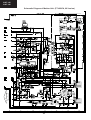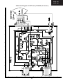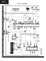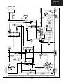
1
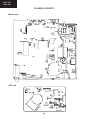
21HT-15C
21HT-16C
SERVICE MANUAL
SE0021HT1*C00
Issued: 14th Nov 2002
GA-1E CHASSIS
PAL SECAM B/G, D/K SYSTEM COLOUR TELEVISION
MODELS
21HT-15CS
21HT-16CS
In the interests of user safety (required by safety
regulations in some countries) the set should restored
to its original condition and only parts identical to
those specified should be used.
CONTENTS
ELECTRICAL SPECIFICATIONS ..................... 3
IMPORTANT SERVICING NOTES .................. 4
CONTROLS & TERMINALS ............................. 5
SERVICE ADJUSTMENTS .............................. 6
HOTEL MODE FUNCTIONS .......................... 12
CHASSIS LAYOUTS .......................................14
LED FLASHING CODE ...................................15
PRINTED WIRING BOARDS ........................... 15
ICs ADDITIONAL INFORMATION ..................20
SCHEMATIC DIAGRAMS .............................. 26
BLOCK DIAGRAMS ....................................... 32
TROUBLESHOOTING TABLES ...................... 35
PARTS LISTING .............................................. 38
CRT ADAPTATION ........................................ 42
SOURCE OF DOCUMENTATION ................. 43
SHARP CORPORATION This document has been published to
1
be used for after sales service only.
21HT-15C
21HT-16C
Service Manual update log sheet
Technical Report No.
Technical Bulletin No.
Cause / Solution
Part No.
Page No.
Application
Data /Serial No.
Use this page to keep any special servicing information as Technical Report (Bulletin), Technical Information, etc.
If only part number changes are required, just change part number directly the part number in the Parts Listing Section.
If you need more information, please refer to the Technical Report (Bulletin).
2
21HT-15C
21HT-16C
ELECTRICAL SPECIFICATIONS
•Power Input .................... 220V-240 Volts AC 50Hz
•Sound Carrier Trap
B/G ................................................ 33.4MHz
D/K ................................................ 32.4MHz
•Power Consumption
Normal Operation (Method IEC60107) ........ 43W
Stand-by Operation .................................. 3W
•Adjacent Sound Carrier Trap
B/G ................................................ 40.4MHz
D/K ................................................ 40.4MHz
•Audio Power Output Rating .............. 4W x 1 (MPO)
•Adjacent Picture Carrier Trap
•Speaker ............................ 16Ω 4W, 9 x 5 cm, 1pc
B/G ............................................... 31.9MHz
D/K ............................................... 30.9MHz
•Convergence ................... Self Converging System
•Aerial Input Impedance
•Focus ............................... Bi-Potential Electrostatic
VHF/UHF .................... 75 ohm Unbalanced
•Sweep Deflection ..................................... Magnetic
•Tuning Ranges ......... 48.25MHz thru 855.25 MHz
VHF ......................... CH02-CH12, R01-R12
S1-S41 (HYPERBAND)
UHF ....................................... CH21 - CH69
•Picture Intermediate Frequency
B/G ................................................. 38.9MHz
D/K ................................................. 38.9MHz
•White Level
Set the brightness control, with no signal connected, so that the CRT cathode current is 600µA. The maximum
correction applied to each cathode current to achieve a screen temperature of 7250 degrees K-11 MPCD
should not exceed 15% of its original value.
X
Y
Screen temperature
0.304 + 0.015
0.306 + 0.015
7250º K-11 MPCD
Specifications are subject to change without prior notice.
MODEL DIFFERENCES AND DESTINATION (Operation Manual languages)
21HT15C:
21HT15CS:
21HT16C:
21HT16CS:
English, Polish, Russian, Czech, Slovak, Hungarian, Romanian.
Silver Cab. English, Polish, Russian, Czech, Slovak, Hungarian, Romanian.
Cyrillic European TXT. English, Polish, Russian, Czech, Slovak, Hungarian, Romanian.
Cyrillic European TXT, Silver Cab. English, Polish, Russian, Czech, Slovak, Hungarian,
Romanian.
WARNING
The chassis in this receiver is partially hot. Use an isolation transformer between the line cord plug and
power receptacle, when servicing this chassis.
To prevent electric shock, do not remove cover. No user-serviceable parts inside. Refer servicing to
qualified service personnel.
3
21HT-15C
21HT-16C
IMPORTANT SERVICING NOTES
Only qualified service personnel are allowed to carry out maintenance and repair of this receiver.
Servicing of high voltage system and CRT
It is important that the static charge is removed from the high voltage system when carrying out work on the
receiver. This can be achieved by connecting a 10K resistor (with a suitably insulated lead) from the CRT cavity
connector to the CRT ground tag. This must be carried out with the AC supply disconnected from the receiver.
Note the following:
• The CRT in this receiver employs Integral Implosion Protection.
• If the CRT has to be changed it MUST be replaced with the correct type for continued safe working
• DO NOT lift the CRT by its neck.
• When handing the CRT, ensure that shatterproof goggles are worn.
• Ensure that the CRT is discharge before handling.
X-Ray
This receiver is designed to keep any x-ray emission to an absolute minimum. Some fault conditions and
servicing procedures may produce potentially hazardous x-ray radiation levels. This is a problem when in close
proximity to the receiver for long periods of time. To reduce any risks associated with this, please observe the
following precautions:
1. When undertaking any servicing on this chassis, DO NOT increase the EHT to more than 30.5 KV,
(at a instantaneous beam current of 1300µA).
2. Ensure that during normal operation the EHT does not exceed 25.0 KV±1.5KV (at a beam current of
1100µA). This level has been preset in the factory. Always check that this level has not been exceeded after
carrying out any repair on the receiver.
3. DO NOT replace the CRT with any other type than that specified in the parts listing as this may
cause excessive x-ray radiation.
Before returning the receiver to the customer
In addition to the above checks, the following should also be carried out before returning the receiver to the
customer.
1. Inspect all the leads to ensure that they are dressed correctly and that they are not obstructed or
pinched by any other parts.
2. Ensure that all protective devices are in good condition. These will include nonmetallic control
knobs, insulating fish papers, cabinets backs, compartment covers or shields, mechanical insulators, etc.
4
21HT-15C
21HT-16C
CONTROLS & TERMINALS
Remote Control
CALL (
)/CHILD LOCK (
SOUND MUTE (
POWER/STANDBY (
Infrared Transmitter Window
Aim this window at the infrared sensor
on your TV set
) button
) button
TV/VIDEO Select button
) button
Single/Double Entry button (
TV/VIDEO
Programme Select buttons
FLASHBACK ( ) button
Returns to previously viewed
programme
1
2
3
4
5
6
7
8
9
6CHANNEL (PROGRAMME) UP (
)/
DOWN ( ) button
( ) Selects next higher programme
( ) Selects next lower programme
(These are also used for menu
set up)
0
MENU
VOLUME UP ( )/DOWN ( ) button
( ) Increases sound
( ) Decreases sound
(These are also used for menu set up)
CLOCK (
REVEAL (
HALF PAGE (
COLOUR buttons
button (Teletext)
?
RESET (
i
i
INDEX (
I
S
) button (Teletext)
X)
LIST
HOLD (
I
) button (Teletext)
) button (Teletext)
LIST
25Select button (Teletext)
button (Teletext)
) button (Teletext)
)
CH
X
CANCEL (
Text/Mix/Picture (
Select button (Teletext)
CH
) button (Teletext)
?)
)
TV/TEXT REMOTE CONTROL
STORE (
S
) button (Teletext)
TV Front
MENU
Power (
CH
) button
Channel Up (
Power/On Timer indicator
Volume Up (
Remote Control Sensor
)/Down (
)/Down (
) buttons
) buttons
Menu button
Euro-SCART 21-Pin Terminal
21-Pin Euro-SCART
For greater A/V enjoyment, various audio and video devices may be
connected via the Euro-SCART 21-Pin Terminal.
1.
2.
3.
4.
5.
6.
Audio right output
Audio right input
Audio left output
Common earth for audio
Earth for blue
Audio left input
7. Blue input
8. Audio-video control
9. Earth for green
10. Not used
11. Green input
12. Not used
13. Earth for red
14. Not used
15. Red input
16. Red/Green/Blue control
17. Earth for video
18. Earth for video
5
19. Video output
20. Video input
21. Plug shield
21HT-15C
21HT-16C
SERVICE ADJUSTMENTS
• Service Mode function
All required adjustments for servicing this TV set, may be done in “service mode”, excepting G2 and FOCUS.
How to access the Service Mode
1.
Turn the receiver on and ensure that it is tuned into a test pattern.
2.
Turn the receiver off using the mains switch.
3.
Press the volume down and channel up buttons together. See Fig.1.
4.
Continue pressing the volume down and channel up buttons while turning
the mains on using the mains switch. See Fig.1.
5.
Keep pressing the volume down and channel up buttons until the picture appears.
6.
When <<SHARPX X VXX.XX>> appears on the screen, release the two buttons.
7.
The receiver is now in the service mode.
Fig. 1
To move between the various service mode functions, use the channel up and down buttons.
Use the volume buttons to change the data to the desired value.
The data will be stored automatically when exiting the service mode. To exit the service mode press the stand-by button on the remote control or turn the receiver off with the mains switch.
Fig. 2
Fig. 3
SHARP X
X VXX.XX
STS0: XXXX XXXX
STS1: XXXX XXXX
STS2: XXXX XXXX
Adjustment
(Yellow)
6
XXXX:
XX:
Value
(Green)
21HT-15C
21HT-16C
• Service adjustment and data list
The table below shows the various service mode positions, range of values and default value. The columns are headed
as below.
Heading:
Descriptions:
OSD
This is what will appear on the screen at this position.
Function
This is the description of the mode’s function.
Range
This is the range of values that can be entered while in this mode.
Initial
This is the initial value, i.e. just after changing the NVM. Shadowed values are those to be modified in
Default.
Default
This is the recommended default value for this mode.
FIX/ADJ
If this is ADJ, then it may be necessary to adjust this value away from the default.
No. OSD
Function
Range
Initial
Default
FIX/ADJ
1
AGC
AGC Take Over Point
0...63
14
34
ADJ
2
V-LIN
Vertical Slope [VS]
0...63
32
33
ADJ
3
V-AMP
Vertical Amplitude [VA]
0...63
32
18
ADJ
4
V-CENT
Vertical Shift [VSH]
0...63
32
17
ADJ
5
H-CENT
Horizontal shift [HS]
0...63
32
34
ADJ
6
H-CENT60
offset to H-CENT for60 Hz
0...31 data(-16..+15)
16
20
FIX
7
EW / /
Horizontal Parallelogram [HP]
0...63
32
32
FIX
8
HB
Horizontal Bow
0...63
32
32
FIX
9
S-COR
S-Correction [SC]
0...63
0
22
FIX
10
DRI-RS
White point Red Standard white temp.
0...63
32
42
ADJ
11
DRI-GS
White point Green Standard white temp. 0...63
32
42
ADJ
12
DRI-BS
White point Blue Standard white temp
0...63
32
42
ADJ
13
DRI-RW
White point Red Warm white temp.
0...32
16
16
FIX
14
DRI-GW
White point Green Warm white temp.
0...32
16
9
FIX
15
DRI-BW
White point Blue Warm white temp.
0...32
16
9
FIX
16
DRI-RC
White point Red Cold white temp.
0...32
16
9
FIX
17
DRI-GC
White point Green Cold white temp.
0...32
16
9
FIX
18
DRI-BC
White point Blue Cold white temp.
0...32
16
16
FIX
19
SUB-VOL
Max Volume
0...63
60
60
FIX
20
SUB-CON
Sub Contrast
0...63
63
63
FIX
21
SUB-COL
Sub Colour
0...63
32
25
FIX
22
SUB-BRI
Sub Brightness
0...63
32
34
FIX
23
TINT
Sub Tint
0...63
32
32
FIX
24
SUB-SHP
Sub Sharpness
0...63
32
11
FIX
25
HTL-VOL
Max Hotel Volume
0...63
30
30
FIX
7
21HT-15C
21HT-16C
No. OSD
Function
Range
Initial
Default
26
27
28
29
30
31
32
33
34
35
36
37
38
39
40
41
42
43
44
45
46
HTL-PRG
RGB
SEARCH-SYS
CUT-R
CUT-G
CDL
DL-PT
DL-ST
DL-4T
COL-OP
COL-OS
COL-O4
SHP-OP
SHP-OS
SHP-O4
SC-VOL
PRE-SC
PRE-FM
PRE-NICAM
AVC-DKY
AC-OFF-TIM
0...99 or > 99 for none
0...15
0(L-BG),1(BG),2(I),3(DK)
0...63
0...63
0...15
0...15
0...15
0...15
0...15
0...15
0...15
0...15
0...15
0...15
0..255
0..127
0..127
0..127
1...4 data(1.2.4.8.)
0..15
255
15
1
0
0
0
12
15
12
8
8
4
8
4
8
115
25
72
0
2
0
255
0
3
0
10
5
4
8
8
8
8
4
8
4
8
115
25
72
0
2
0
FIX
FIX
FIX
FIX
FIX
FIX
FIX
FIX
FIX
FIX
FIX
FIX
FIX
FIX
FIX
FIX
FIX
FIX
FIX
FIX
FIX
47
DISP
Hotel Program number
OSD RGB Reference
Sound system for auto turning
Black Level off-set R [BLR]
Black Level off-set G (BLG)
Cathode Drive Level [CL]
Y-Delay time for PAL (TV) [YD]
Y-Delay time for SECAM (TV) [YD]
Y-Delay time for N443 (TV) [YD]
COLOUR OFFSET (PAL)
COLOUR OFFSET (SECAM)
COLOUR OFFSET (NTSC443)
SHARPNESS OFFSET(PAL)
SHARPNESS OFFSET(SECAM)
SHARPNESS OFFSET(NTSC443)
SCART volume
Prescaler SCART input
Prescaler FM/AM
Prescaler SCART input
AVC Decay
Time to set the AC-OFF
timer is in steps of 10minutes
Language or symbols
0
0
FIX
48 TXT-EUR
Teletext pan-European language
49
50
51
52
53
54
55
56
57
58
59
60
61
62
63
64
65
66
67
68
69
70
71
72
73
74
75
Black Stretch
Automatic Volume Control(AVL)
Fast Filter IF-PLL
Auto Colour Limit
Sound system L
Sound system DK
Sound system I
Sound system BG
Video mute at Ident loss
Video Mute at program/source Change
Hotel mode
Reduced FM demodulator Gain (for BTSC sig)
Number of external AV sources
FM Window Selection
Sound Mute bit 0
Sound Mute bit 1
IF AGC speed bit0
IF AGC speed bit1
Phi 1 time constant for FE(RF)
Phi 2 time constant for FE(RF)
Phi 1 time constant for AV
Phi 2 time constant for AV
Teletext
Teletext Western or Eastern characters
Forced V-SYNC slicing level
Sync of OSD
Charge pump
BKS
AVC
FFI
ACL
S-L
S-DK
S-I
S-BG
BLUE-BACK
VMC
HTL
BTSC
AV
FMWS
SM0
SM1
AGC0
AGC1
FOA-FE
FOB-FE
FOA-AV
FOB-AV
TXT
TXT-W/E
FSL
HP2
CP
76 NICAM
77 IGR
78 AUTO
79 TXT-TGL
80 EVG
NICAM decoding enabled
IGR decoding enabled
Start auto tuning at POWER-ON
Function of TXT key
Enable Vertical Guard
8
0(symboles),
1(English),
2(French)
0 (teletext pan-european language)
1 (second language;cyrillic)
2(third language;Greek)
0 (disable) or 1 (enable)
0 (disable) or 1 (enable)
0 (disable) or 1 (enable)
0 (disable) or 1 (enable)
0 (disable) or 1 (enable)
0 (disable) or 1 (enable)
0 (disable) or 1 (enable)
0 (disable) or 1 (enable)
0 (disable) or 1 (enable)
0 (disable) or 1 (enable)
0 (disable) or 1 (enable)
0 (disable) or 1 (enable)
0 for 1 AV or 1 for 2 AV
0 (disable) or 1 (enable)
0 (disable) or 1 (enable)
0 (disable) or 1 (enable)
0 (disable) or 1 (enable)
0 (disable) or 1 (enable)
0 (disable) or 1 (enable)
0 (disable) or 1 (enable)
0 (disable) or 1 (enable)
0 (disable) or 1 (enable)
0 (disable) or 1 (enable)
0 (westem) or 1 (eastem)
0 (disable) or 1 (enable)
0 for Ph1 or 1 for Ph2
0 (fast tuning) or
1 (moderate speed tuning)
0 (disable) or 1 (enable)
0 (disable) or 1 (enable)
0 (disable) or 1 (enable)
0 or 1
0 (disable) or 1 (enable)
FIX/ADJ
0
0 (...15C) FIX
0
1
0
0
0
0
1
1
1
1
1
0
0
1
0
1
0
1
0
0
0
1
1
0
0
0
0
0
1 (...16C)
1
1
0
1
0
1
0
1
1
1
0
0
0
0
1
0
1
0
0
0
1
1
1
1
0
0
0
0
0
0
0
1
0
0
0
1
1
FIX
FIX
FIX
FIX
FIX
FIX
FIX
FIX
FIX
FIX
FIX
FIX
FIX
FIX
FIX
FIX
FIX
FIX
FIX
FIX
FIX
FIX
FIX
FIX
FIX
FIX
FIX
FIX
FIX
FIX
FIX
FIX
21HT-15C
21HT-16C
• Screen adjustment
1. G2 Adjustment
1.
Enter the service mode (see page 6).
2.
Use the channel up or channel down buttons to enter the << BLUE-BACK >>
function.
3.
Set this to << BLUE-BACK: 0 >>, i.e. blue background is turned off.
4.
Turn the set off at the mains.
5.
Turn the set back on.
6.
Set the picture control settings to normal.
7.
Select the SCART input by pressing the TV/SCART button on the remote control. Do not connect an input to the SCART socket. A blank raster will appear.
8.
Connect an oscilloscope to TP851 on the CRT PWB. The waveform as in figure 4 should be displayed.
9.
Fig. 4
Adjust the G2 control (screen voltage) so that the peak of this waveform is 3.0V
+/-0.1V above the zero volt line.
10. Enter the service mode.
11. Turn the blue background function back on again - set << BLUE-BACK: 1 >>.
12. Turn off the receiver using the mains button.
13. The G2 adjustment is now complete.
2. Focus Adjustment
1.
Receive a monoscope pattern signal at a level of 60 to 80 dBµV.
2.
Set the picture settings to normal.
3.
Adjust the focus potentiometer to obtain maximum definition.
• AGC Adjustment
1.
Tune the receiver into a colour bar signal on channel E-12.
2.
Set the RF generator to an output signal strength of 59 dB/µV (+/-1dBµV) –75 Ohms.
3.
Connect an oscilloscope to TP201. TP201 is one end of R201.
4.
Enter the service mode (see page 6).
5.
Use the channel up and channel down buttons to enter the AGC mode.
6.
By using the volume up and the volume down buttons, adjust the AGC until the voltage on TP201 drops by 0.1V
to 0.3V below its maximum value.
7.
Change the input signal strength to 66-70dBµV and make sure that there is no noise apparent in the picture.
8.
Turn the receiver off at the mains, this will exit the service mode and store the adjustment.
9
21HT-15C
21HT-16C
• Geometry adjustment procedure
To adjust the geometry, follow the procedure outlined below:
1. Tune the set into a Philips test pattern.
2. Enter the service mode as described on page 6.
3. Use the channel up or channel down buttons to enter the desired mode
4. Use the volume buttons to achieve correct setting.
5. When adjustments are complete, use the stand-by button to turn off the set. The adjustment values will be stored
at this point.
V-LIN
Adjust the vertical linearity control so that the picture centring is as shown in figure 5.
Fig. 5
V-AMP
Adjust the vertical amplitude control so that the picture overscans as shown in figure 6.
Fig. 6
V-CENT
Adjust the vertical centring control so that the picture is centred as shown in figure 7.
Fig. 7
H-CENT
Adjust the horizontal centring control so that the picture is centred as shown in figure 8.
Fig. 8
10
21HT-15C
21HT-16C
• Colour adjustment procedure
The following adjustments should only be carried out when the CRT or IC801 are replaced.
Notes:
• This adjustment must be done after warming up the unit for 30 minutes or longer with a beam current over 700 µA.
• The red value «DRI-RS» should be fixed to 42. (Refer to “How to access service mode” section).
• «DRI-GS» adjustment alters “Y” coordinate.
• «DRI-BS» adjustment alters “X” and “Y” coordinates.
Adjustment method 1 (using the signal generator, varying the picture signal)
1.
2.
3.
4.
5.
Adjust G2.
Input a white pattern with burst signal from SCART.
Position the colorimeter in the centre of screen.
Adjusting input signal level, select a luminance of 70 nits.
Operate again in “service mode“ and select «DRI-GS» and/or «DRI-BS» locations to obtain colour coordinates:
X
Y
Screen temperature
0.304 + 0.015
0.306 + 0.015
7250º K-11 MPCD
6. Reset the T V with the mains switch button to store the adjustment and exit service mode.
7. Check colour coordinates “X” and “Y” at 20 a 120 Nits. It may be necessary to repeat the same procedure to
obtain the above values.
Adjustment method 2 (using the signal generator, with a fixed picture signal)
1.
2.
3.
4.
5.
Adjust G2.
Tune a white pattern with burst signal.
Operate in “service mode”:
Using «SUB-CON», select a luminance of 70 nits.
Operate again in “service mode“ and select «DRI-GS» and/or «DRI-BS» locations to obtain colour coordinates:
X
Y
Screen temperature
0.304 + 0.015
0.306 + 0.015
7250º K-11 MPCD
6. Select «SUB-CON». Return data to “63”.
7. Reset the TV with the mains switch button to store the adjustment and exit service mode.
8. Check colour coordinates “X” and “Y” at 20 a 120 Nits. It may be necessary to repeat the same procedure to
obtain the above values.
11
21HT-15C
21HT-16C
HOTEL MODE FUNCTIONS
The following procedure details how to set up the Hotel Mode Functions.
1. Short Description
1.1. Hotel Mode “HTL”: Main Hotel Mode. It deactivates “Channel Setting” functions. It reduces the Maximum Volume.
1.2. Hotel Mode “HTL-VOL”: Maximum Volume Level Regulation.
1.3 Hotel Mode “HTL-PRG”: Fixing start up program when the TV set is switched on.
2. Before start
2.1. It is necessary to program “Channel Setting” before setting up Hotel Mode “HTL” because after that Channel
Setting are deactivated.
2.2. Consider that regarding TXT Features, after activate any of the Hotel modes in the “List Mode” will not be stored
any page.
2.3. Consider that changed video control values are not stored.
3. Procedure
3.1. Hotel Mode “HTL” (Main Hotel Mode).
3.1.1. Previous Service Information: Initial Value: 0. Range: 0 to 1. Service Mode Indication: HTL.
3.1.2. Access the Service Mode (see this procedure on page 6).
3.1.3. Select “HTL” by using channel up/down buttons.
3.1.4. Change initial value from “0” (off ) to “1” (on).
3.1.5. Notes:
3.1.5.1. The maximum volume level has been reduced from 60 to 30. For other value go to 3.2. Hotel Mode
“HTL-VOL”
3.1.5.2. “Channel Setting” functions have been deactivated.
3.1.5.3. It is necessary to select Hotel Mode “HTL” to be able to set up Hotel Mode “HTL-VOL” or Hotel Mode
“HTL-PRG”.
3.1.5.4. If you do not need to set up Hotel Mode “HTL-VOL” or “HTL-PRG” get out from Service Mode (To
exit the Service Mode press the stand-by button on the remote control or turn the receiver off with
the mains switch).
3.2. Hotel Mode “HTL-VOL” (Maximum Volume Level Regulation)
3.2.1. Previous Service Information: Initial value: 30. Range: 0 to 60. Service Mode indication: HTL-VOL.
3.2.2. To activate this Hotel Mode it is necessary activate previously Hotel Mode “HTL”. Then the maximum volume
level changed fro 60 to 30 as initial value.
12
21HT-15C
21HT-16C
3.2.3. Select “HTL-VOL” by using channel up/down buttons.
3.2.4. Set the value according to your necessities by using volume up/down buttons.
3.2.5. Change initial value from “0” (off ) to “1” (on).
3.2.6. Note: If you do not need to set up Hotel Mode “HTL-PRG” get out from Service Mode (To exit the Service
Mode press the stand-by button on the remote control or turn the receiver off with the mains switch).
3.3. Hotel Mode “HTL-PRG” (Fixing start up program when the TV Set is switched on)
3.3.1. Initial value: 255. Range: 0 to 255. Service Mode indication: HTL-PRG.
3.3.2. To activate this Hotel Mode it is necessary activate previously Hotel Mode “HTL”.
3.3.4. Select “HTL-PRG” by using channel up/down buttons.
3.3.3. The initial value to 255, ensures that the TV Set starts up in the same program number that it was been
displayed before turn it off.
3.3.4 If you want to fix other program number proceed as follows set the value according to your necessities by
using volume up / down buttons. Use values between 0 to 99. In this way, the new program number appear
fixed when you start up the TV set.
Example: If you would like to set starting program number “2”, change from 255 to 2.
3.3.5. Get out from Service Mode (To exit the Service Mode press the stand-by button on the remote control or turn
the receiver off with the mains switch).
13
21HT-15C
21HT-16C
CHASSIS LAYOUTS
Mother unit
21HS50C
21HS50F
21HS50C
CRT unit
14
21HT-15C
21HT-16C
LED FLASHING CODE
PURPOSE: The led indicates the power mode, occurred I2C error and On timer
INPUT:
Current power mode
- I2C Errors
- On timer
Processing: - If in STANDBY mode and On timer inactive then switch LED off.
- If in STANDBY and On timer active set LED to blinking, (switch on and off at 1 Hz with a
50% duty cycle).
- If in POWER-ON mode, switch LED on.
- If an I2C error occurred, let the LED blink at 1 Hz, 50 % duty cycle.
For the blinking times see the Table below.
Note: Only when an I2C error occurs for a number of times, or for a number of seconds, the I 2C error is
handled by the system (that is ,only then the set will go to standby, the led starts blinking).
IC/Module Name
Slave Address
M24C04, M24C08
TDA935x/6x/8x
VTST6HD64 or
CTF551
Bus Error LED Remarks
Blinking Time
A0,A2
8A
C0
C0
2
3
6
6
Ref. No.
512x8 EEPROM,1024x8 EEPROM
Address of internal TV processor
PLL Tuner
Table Error LED blinking times
PRINTED WIRING BOARDS
F 7341N0 PWB. Components side.
6
5
4
3
2
1
Y
0
X
1
2
3
4
5
15
6
7
8
9
10
IC1002
IC801
TU201
21HT-15C
21HT-16C
F 7340N7A PWB. Component side
25
24
23
22
21
20
19
18
17
16
15
14
13
12
11
10
9
8
7
6
5
4
3
Page 17
2
1
Y
0
X
1
2
3
4
5
6
7
16
8
9
10
11
12
13
21HT-15C
21HT-16C
F 7340N7A PWB. Component side
25
24
23
22
21
20
19
18
17
16
15
14
13
12
11
10
9
8
7
6
5
4
Page 16
3
2
1
Y
12
13
14
15
16
17
18
17
19
20
21
22
23
24
X
25
21HT-15C
21HT-16C
F 7340N7A PWB. Copper side
25
24
23
22
21
20
19
18
17
16
15
14
13
12
11
10
9
8
7
6
5
4
3
Page 19
2
1
Y
0
X
1
2
3
4
5
6
7
18
8
9
10
11
12
13
21HT-15C
21HT-16C
F 7340N7A PWB. Copper side
25
24
23
22
21
20
19
18
17
16
15
14
13
12
11
10
9
8
7
6
5
4
Page 18
3
2
1
Y
12
13
14
15
16
17
18
19
19
20
21
22
23
24
X
25
21HT-15C
21HT-16C
ICs ADDITIONAL INFORMATION
TDA9351(IC801)
QUICK REFERENCE DATA
SYMBOL
PARAMETER
MIN.
TYP.
MAX.
UNIT
Supply
VP
supply voltages
−
8.0/3.3
−
V
IP
supply current
−
135/60
−
mA
ViVIFrms)
video IF amplifier sensitivity (RMS value)
−
75
−
µV
ViSIF(rms)
QSS sound IF amplifier sensitivity (RMS value)
−
60
−
µV
Input voltages
ViAUDIO(rms)
external audio input (RMS value)
−
500
−
mV
ViCVBS(p-p)
external CVBS/Y input (peak-to-peak value)
−
1.0
−
V
ViCHROMA(p-p)
external chroma input voltage (burst amplitude)
(peak-to-peak value)
−
0.3
−
V
ViRGB(p-p)
RGB inputs (peak-to-peak value)
−
0.7
−
V
ViYIN(p-p)
luminance input signal (peak-to-peak value)
−
1.4
−
V
ViUVIN(p-p)
U/V input signal (peak-to-peak value)
−
1.33/1.05 −
V
Output signals
Vo(IFVO)(p-p)
demodulated CVBS output (peak-to-peak value)
−
2.5
−
V
Vo(QSSO)(rms)
sound IF intercarrier output in QSS versions (RMS value)
−
100
−
mV
Vo(AMOUT)(rms) demodulated AM sound output in QSS versions (RMS
value)
−
500
−
mV
Io(AGCOUT)
tuner AGC output current range
0
−
5
mA
VoRGB(p-p)
RGB output signal amplitudes (peak-to-peak value)
−
2.0
−
V
IoHOUT
horizontal output current
10
−
−
mA
IoVERT
vertical output current (peak-to-peak value)
1
−
−
mA
IoEWD
EW drive output current
1.2
−
−
mA
SECPLL
VSSA
P0.6
P0.5
VSSC/P
P3.3/ADC3
P3.2/ADC2
P3.1/ADC1
P3.0/ADC0
P2.0/TPMW
P1.7/SDA
P1.6/SCL
P1.3/T1
15
14
13
12
11
10
9
8
7
6
5
4
3
2
1
56
57
58
59
60
61
62
63
64
VDDC
OSCGND
XTALIN
XTALOUT
RESET
VDDP
P1.0/INT1
P1.1/T0
P1.2/INT0
handbook, halfpage
VP2
16
DECDIG
PH2LF
17
18
PH1LF
GND3
19
20
DECBG
23
21
24
AVL/EWD
IFIN1
25
22
IFIN2
VDRB
VDRA
IREF
26
27
29
VSC
30
TUNERAGC
AUDEEM/SIFIN1
DECSDEM/SIFIN2
31
28
SNDPLL/SIFAGC
32
GND2
AVL/SNDIF/
REFO/AMOUT
XXX
MXXxxx
49
50
51
52
53
54
55
B2/UIN
BCLIN
BLKIN
RO
GO
BO
VDDA
VPE
G2/YIN
48
47
CHROMA
R2/VIN
CVBS/Y
46
43
GND1
45
42
CVBSINT
AUDOUT/AMOUT
41
INSSW2
40
VP1
44
39
IFVO/SVO
PLLIF
EHTO
AUDEXT/QSSO/
AMOUT
FBISO
HOUT
38
37
36
35
34
33
Pin configuration (SDIP 64)
TDA935X/6X/8X PS/N2
20
42
40
24
21
+8V
15
19
14
39
18
41
30
(32)
13
CHROMA 43
CVBS/Y
IFIN
23
27
37
38
SNDIF
17
H-OSC. + PLL
H/V SYNC SEP.
DECODER
PAL/SECAM/NTSC
REF
VIDEO FILTERS
VIDEO IDENT.
VIDEO SWITCH
VISION IF
ALIGNMENT-FREE
PLL DEMOD.
AGC/AFC
VIDEO AMP.
TUNERAGC
AUDEXT
35
34
H-SHIFT
16
2nd LOOP
H-DRIVE
DELAY LINE
BASE-BAND
AGC CIRCUIT
NARROW BAND
PLL
DEMODULATOR
AUDOUT
V
44
HOUT
33
AUDIO SWITCH
(AVL)
VOLUME CONTROL
DEEMPHASIS
(20) 29 28
(32)
VPE
25
26
21
V-DRIVE
22
GEOMETRY
V-DRIVE +
LUMA DELAY
PEAKING
BLACK STRETCH
ROM/RAM
80C51 CPU
36
CVBS
LED OUT (2x)
EHTO
58 57
ENHANCED
60 55 59
3
4
5-8
ADC IN (4x)
VST OUT
I/O PORTS (4x)
EWD
(20)
(EW GEOMETRY)
SYNC
ACQUISITION
TELETEXT
I/O PORTS
VST PWM-DAC
I2C-BUS
TRANSCEIVER
2
1+62-64
RESET
V
U
Y
MEMORY
1/10 PAGE
54 56 61
G
B BL
B0
BCLIN
BLKIN
49
50
WHITE-P. ADJ.
R/V G/Y B/U BL
46 47 48 45
SATURATION
YUV/RGB MATRIX
RGB/YUV MATRIX
RGB/YUV INSERT
R G B
GO
53
RO
51
OSD/TEXT INSERT
CCC
CONTR/BRIGHTN
R
DISPLAY
TELETEXT/OSD
12
+3.3 V
52
COR
V
H
9
Block diagram TDA935X/6X8X PS/N2 with mono intercarrier sound demodulator
H
REF
(32) 31
SCL SDA
10/11
SOUND
TRAP
21HT-15C
21HT-16C
TDA9351(IC801)
BLOCK DIAGRAM
21HT-15C
21HT-16C
TDA9351(IC801)
PINNING
SYMBOL
PIN
DESCRIPTION
P1.3/T1
P1.6/SCL
P1.7/SDA
P2.0/TPWM
P3.0/ADC0
P3.1/ADC1
P3.2/ADC2
P3.3/ADC3
VSSC/P
P0.5
P0.6
VSSA
SECPLL
VP2
DECDIG
PH2LF
PH1LF
GND3
DECBG
AVL/EWD (1)
VDRB
VDRA
IFIN1
IFIN2
IREF
VSC
TUNERAGC
AUDEEM/SIFIN1(1)
DECSDEM/SIFIN2(1)
GND2
SNDPLL/SIFAGC(1)
AVL/SNDIF/REF0/
AMOUT(1)
HOUT
FBISO
AUDEXT/
QSSO/AMOUT(1)
EHTO
PLLIF
IFVO/SVO
VP1
CVBSINT
GND1
CVBS/Y
CHROMA
AUDOUT /AMOUT(1)
1
2
3
4
5
6
7
8
9
10
11
12
13
14
15
16
17
18
19
20
21
22
23
24
25
26
27
28
29
30
31
32
33
34
35
port 1.3 or Counter/Timer 1 input
port 1.6 or I2C-bus clock line
port 1.7 or I2C-bus data line
port 2.0 or Tuning PWM output
port 3.0 or ADC0 input
port 3.1 or ADC1 input
port 3.2 or ADC2 input
port 3.3 or ADC3 input
digital ground for µ-Controller core and periphery
port 0.5 (8 mA current sinking capability for direct drive of LEDs)
port 0.6 (8 mA current sinking capability for direct drive of LEDs)
analog ground of Teletext decoder and digital ground of TV-processor
SECAM PLL decoupling
2nd supply voltage TV-processor (+8V)
decoupling digital supply of TV-processor
phase-2 filter
phase-1 filter
ground 3 for TV-processor
bandgap decoupling
Automatic Volume Levelling /East-West drive output
vertical drive B output
vertical drive A output
IF input 1
IF input 2
reference current input
vertical sawtooth capacitor
tuner AGC output
audio deemphasis or SIF input 1
decoupling sound demodulator or SIF input 2
ground 2 for TV processor
narrow band PLL filter /AGC sound IF
Automatic Volume Levelling / sound IF input / subcarrier reference output /AM output
(non controlled)
horizontal output
flyback input/sandcastle output
external audio input /QSS intercarrier out /AM audio output (non controlled)
36
37
38
39
40
41
42
43
44
EHT/overvoltage protection input
IF-PLL loop filter
IF video output / selected CVBS output
main supply voltage TV-processor (+8 V)
internal CVBS input
ground 1 for TV-processor
external CVBS/Y input
chrominance input (SVHS)
audio output /AM audio output (volume controlled)
22
21HT-15C
21HT-16C
TDA9351(IC801)
SYMBOL
INSSW2
R2/VIN
G2/YIN
B2/UIN
BCLIN
BLKIN
RO
GO
BO
VDDA
VPE
VDDC
OSCGND
XTALIN
XTALOUT
RESET
VDDP
P1.0/INT1
P1.1/T0
P1.2/INT0
PIN
45
46
47
48
49
50
51
52
53
54
55
56
57
58
59
60
61
62
63
64
DESCRIPTION
2nd
RGB / YUV insertion input
2nd R input / V (R-Y) input
2nd G input / Y input
2nd B input / U (B-Y) input
beam current limiter input / (V-guard input, note 2)
black current input / (V-guard input, note 2)
Red output
Green output
Blue output
analog supply of Teletext decoder and digital supply of TV-processor (3.3 V)
OTP Programming Voltage
digital supply to core (3.3 V)
oscillator ground supply
crystal oscillator input
crystal oscillator output
reset
digital supply to periphery (+3.3 V)
port 1.0 or external interrupt 1 input
port 1.1 or Counter/Timer 0 input
port 1.2 or external interrupt 0 input
Note
1. The function of pin 20, 28, 29, 31, 32, 35 and 44 is dependent on the IC version (mono intercarrier FM demodulator
/ QSS IF amplifier and East-West output or not) and on some software control bits. The valid combinations are given
in table 1.
2. The vertical guard function can be controlled via pin 49 or pin 50. The selection is made by means of the IVG bit in
subaddress 2BH.
Table 1
Pin functions for various versions
IC version
FM-PLL version
QSS version
East-West Y/N
N
Y
N
Y
CMB1/CMB0 bits
00
01/10/11
00
01/10/11
00
01/10/11
00
01/10/11
AM bit
−
−
−
−
−
0
1
−
0
1
Pin 20
AVL
EWD
AVL
EWD
Pin 28
AUDEEM
SIFIN1
Pin 29
DECSDEM
SIFIN2
Pin 31
SNDPLL
SIFAGC
REFO(2)
AMOUT
REFO(2)
Pin 32
SNDIF(1) REFO(2) AVL/SNDIF(1) REFO(2) AMOUT
Pin 35
AUDEXT
AUDEXT QSSO AMOUT AUDEXT QSSO AMOUT
Pin 44
AUDOUT
controlled AM or audio out
Note
1. When additional (external) selectivity is required for FM-PLL system pin 32 can be used as sound IF input. This
function is selected by means of SIF bit in subaddress 28H.
2. The reference output signal is only available for the CMB1/CMB0 setting of 0/1. For the other settings this pin is a
switch output (see also table 67).
23
21HT-15C
21HT-16C
TEA1507(IC701)
ndbook, full pagewidth
VCC
1
SUPPLY
MANAGEMENT
8
START-UP
CURRENT SOURCE
clamp
internal UVLO start
supply
GND
2
S1
7
VALLEY
DRAIN
HVS
n.c.
M-level
4
VOLTAGE
CONTROLLED
OSCILLATOR
LOGIC
DEM
100 mV
OVERVOLTAGE
PROTECTION
FREQUENCY
CONTROL
OVERTEMPERATURE
PROTECTION
CTRL
LOGIC
6
DRIVER
DRIVER
Iss
3
−1
POWER-ON
RESET
S
Q
R
Q
LEB
blank
UVLO
2.5 V
0.5 V
soft
start
S2
5
OCP
burst
detect
short
winding
MAXIMUM
ON-TIME
PROTECTION
TEA1507
0.75 V
OVERPOWER
PROTECTION
MGU230
Block diagram.
PINNING
SYMBOL PIN
DESCRIPTION
VCC
1
supply voltage
GND
2
ground
CTRL
3
control input
DEM
4
input from auxiliary winding for
demagnetization timing, OVP and OPP
Isense
5
programmable current sense input
DRIVER
6
gate driver output
HVS
7
high voltage safety spacer, not
connected
DRAIN
8
drain of external MOS switch, input for
start-up current and valley sensing
handbook, halfpage
VCC 1
8 DRAIN
GND 2
7 HVS
TEA1507
CTRL 3
6 DRIVER
DEM 4
5 Isense
MGU231
Pin configuration.
24
Isense
21HT-15C
21HT-16C
AN7523(IC303)
9
Volume
8
7
Pin Descriptions
N.C.
Input
GND
6
5
Standby
4
GND
Output
3
2
Output
VCC 1
Circuit Function Block Diagram
Pin No.
Description
1
Vcc
2
Ch Output (+)
3
GND
4
Ch Output (-)
5
Standby
6
Ch Input
7
GND
8
N.C
9
Volume
Note: Do not apply voltage or current to NC pin from outside
AN5522(IC501)
Pin Descriptions
Circuit Function Block Diagram
Thermal Protection
Amp
Pump Up
2
3
4
5
6
Vcc
Pump Up Out
GND
Output
Output Vcc
7
Non-inverting Input
1
Inverting Input
+
25
Pin No.
Pin Name
1
Inverting Input
2
Power Supply
3
Pump-up Output
4
GND
5
Vertical Output
6
Vertical Output Power Supply
7
Non-inverting Input
21HT-15C
21HT-16C
SCHEMATIC DIAGRAMS
Description
Note:
Safety note:
1. Disconnect the AC plug from the AC outlet before replacing parts.
1. The unit of resistance «ohm»is omitted (K=1000 ohms.
M= Megaohm).
2. All resistors are 1/16 watt. unless otherwise noted.
3. All capacitors are µF, unless otherwise noted (P= µµF).
4. The capacitor with Part No. RC-FZ9XXXBMNJ is designed to with stand 63V.
5. The capacitor with Part No. RC-FZ4XXXBMNJ is designed to with stand 50V.
2. Semiconductor heat sinks should be regarded
as potential shock hazards when the chassis is
operating.
Important safety note:
Service precaution:
The area enclosed by this line is directly (
)
connected with AC mains voltage.
When servicing the area, connect an insulating
transformer between TV receiver and AC line to
eliminate hazard of electric shock.
) are important
Parts marked with « ! » (
for maintaining the safety of the set. Be sure to replace these parts with specified ones for maintaining the safety and performance of the set.
CAUTION
This circuit diagram is original one, therefore
there may be slight difference from yours.
Waveform measurement condition:
Colour bar generator signal of 70 dB from RF input.
Waveforms
26
21HT-15C
21HT-16C
27
21HT-15C
21HT-16C
Schematic Diagram of Mother Unit (F7340N7A, 00 Version)
I
H
G
F
E
D
C
B
Page 29
A
1
2
3
4
28
5
6
7
21HT-15C
21HT-16C
Schematic Diagram of Mother Unit (F7340N7A, 00 Version)
I
H
G
F
E
D
C
B
Page 28
Page 30
A
8
9
10
11
29
12
13
14
21HT-15C
21HT-16C
Schematic Diagram of Mother Unit (F7340N7A, 00 Version)
I
H
G
F
E
D
Page 29
C
B
A
8
9
10
11
30
12
13
14
21HT-15C
21HT-16C
Schematic Diagram of CRT Unit (F7341N0, 00 Version)
I
H
G
F
E
D
C
B
A
1
2
3
4
31
5
6
7
21HT-15C
21HT-16C
BLOCK DIAGRAMS
Mother Unit
I
H
G
F
E
D
C
B
Page 33
A
1
2
3
4
32
5
6
7
21HT-15C
21HT-16C
Mother Unit
I
H
G
F
E
D
C
Page 32
B
A
8
9
10
11
33
12
13
14
21HT-15C
21HT-16C
CRT Unit
I
H
G
F
E
D
C
B
A
1
2
3
4
34
5
6
7
21HT-15C
21HT-16C
TROUBLESHOOTING TABLES
NO RASTER
Check F701
NO
YES
Does F701
appear blown
out?
Replace the fuse
Check T701 pin
16 voltage.
Does F701
appear blown
out again?
NO
Does 290V
appear at pin (16)
of T701 (SMT
Transf.)
NO
YES
END
Check
R701,S701 and
AC in.
NO
YES
Does 110V
appear in
Main+B C752) ?
Check IC701, D701, D702,
D703, D704, C705, Q701
YES
Check F751, D758, C702
IC702, Q752 and R615 line
NO
Check D1001
Does Power LED
bright red Turn on?
NO
Check C878
See Many often D1001
Flashes in red, this indicates which
IC to check up.
YES
Check CRT
connector K1-K5
BIAS
YES
Check IC801
Heater
Explanation:
NVM
(IC1002)
2 Times Flash
TV Processor
(IC801)
3 Times Flash
TUNER
(TU201)
6 Times Flash
Power LED dark red
Protector Circuit
(R1028,D615,D612,D509,D510,D614,D604,D605,Q603)
35
21HT-15C
21HT-16C
NEITHER VERTICAL NOR
HORIZONTAL SYNCHRONIZATION
CIRCUIT TO BE CHECKED:
Sync. Separator Circuit.
Check pin33 and 34
of IC801.
DEFECTIVE VERTICEL AMP.
AND VERTICAL LINEARITY
Readjusted vertical size.
(Bass Data)
Vertical linearity and size
is abnormal.
Check R502,R505
NO VERTICAL SCAN
Check IC501 bias.
Normal
Abnormal
Check C502 and C514.
Check IC501.
NO SPECIFIC COLOUR
NO
YES
Is some colour produced in
B/W broadcast reception?
YES
Check IC801,R801,R802,
R803,D804,D805,D806
and Q801.
Is the white balance
properly adjusted?
NO
Readjusted the white
balance.
The picture colour is cyan.
The picture colour is magenta.
The picture colour is yellow.
Check Q870,Q885 and
their adjacent circuits.
Check Q871,Q883 and
their adjacent circuits.
Check Q872,Q887 and
their adjacent circuits.
36
21HT-15C
21HT-16C
NO PICTURE, NO SOUND
CIRCUITS TO BE CHECKED:
Tuner.
PIF.
Automatic Gain Control.
5V, 32V Power Source.
Does the noise level increase at max.
Contrast,Brightness and Sound controls?
Noise increase but no
signal is received.
No snow noise.
Check the tuner supply voltage
LB and HB must be approx. 5V,
BT must be approx. 32V,and
CH preset data check.
Does noise or signal appear
at pin40 of IC801?
NO
YES
Does noise or
signal appear at
pin38 of IC801?
Normal
NO
Check the tuner
AGC at TP201.
Normal
YES
Does noise or
signal appear at
pin23 and 24
of IC801?
Abnormal
NO
Check pin38
of IC801.
Check pin27
of IC801,Tuner
and related circuit.
Check IC801
and its related
circuit.
Check Q401
Q402 and related
circuit.
YES
Check pin1,2 of
SF201,Tuner
and related
circuit.
Check pin37 of
IC801 and
related circuit.
NO SOUND
CIRCUITS TO BE CHECKED:
Audio Output Circuit.
NO
Does signal appear
at pin6 of IC302/303?
YES
Check IC3001 and
its related circuit.
NO
Check Speaker.
Check IC302/303 and
peripheral circuit.
37
21HT-15C
21HT-16C
PARTS LISTING
REPLACEMENT PARTS
Replacement parts which have special safety characteristics are identified in this manual. Electrical components having such features are
identified by ! in the Replacement Part List.
The use of a substitute replacement part which does not have the same
safety characteristics as the factory recommended is not permitted.
Replacement parts not shown in this service manual may create shock
fire, or other hazards.
HOW TO ORDER REPLACEMENT PARTS
To have your order completed promptly and correctly please supply the
following information.
1. MODEL NUMBER
3. PART NO.
5. CODE
2. REF. NO.
4. DESCRIPTION
6. QUANTITY
MARK *:
SPARE PARTS
DELIVERY SECTION
REF No.
PARTS
DESCRIPTION
VB51EFS83912E
CRT 21" THA51EFS83X391+DYW
RCILG0408BMZZ
LHLDC3009CEFN
LHLDC3500BMFW
LHLDW1514BM00
QEARC0009BMZZ
DEGUSSING COIL
ADG COIL HOLDER
HOLDER
HOLDER UNEX 2233
C.EARTH ELECTROMONTAJES
* SN CODE EX CODE
PICTURE TUBE
!
S BN
CD
S
S
S
S
S
AH
AA
AA
AA
AB
AP
AB
AB
AA
AF
S BG
S AK
BY
AV
S AN
AZ
S
S
S
S
S
S
S
S
AC
AC
AA
AC
AA
AB
AV
AB
AH
AG
AE
AH
AD
AF
BG
AF
S
S
S
S
S
S
S
S
S
S
S
S
S
S
S
S
S
S
S
S
S
S
AA
AA
AA
AA
AA
AA
AA
AA
AA
AA
AA
AC
AA
AA
AA
AA
AC
AA
AA
AA
AA
AA
AA
AA
AA
AA
AA
AA
AA
AA
AA
AA
AC
AK
AA
AA
AA
AA
AH
AA
AA
AA
AA
AA
MISCELLANEOUS PARTS
!
PRINTED WIRING BOARDS (Not replacement item)
DUNTK7340CJV9 ADJUST CHASSIS 21HT15C
DUNTK7341BMV9 CRT UNIT 21HT15C
PWB-A
MOTHER UNIT
TUNER
TU 0201
VTUCTF5511+++ TUNER THOMSON
IC 0303
IC 0501
IC 0601
IC 0701
IC 0702
IC 0751
IC 0801
IC 1002
VHIAN7523++-1
VHIAN5522++-1
VHIKA7808AP-1
VHITEA1507/-1
RH-FX0008GEZZ
VHITA48M033-1
RH-IX3560CEN1
VHIM24C08W6-1
IC AN7523 MATSUSHITA
IC AN5522 MATSUSHITA
IC KIA7808API KOREA ELECTRONICS
IC TEA1507P/N1 PHILIPS
P/COUPLER RANK-S SHARP
IC TA48M033F(S) TOSHIBA
IC TDA9351PS/N2 PHILIPS
IC M24C08-WMN6T ST MICRO
Q
Q
Q
Q
Q
Q
Q
Q
Q
Q
Q
Q
Q
Q
Q
Q
Q
Q
Q
Q
Q
Q
VS2SC3928AR-1
VS2SC3928AR-1
VS2SC3928AR-1
VS2SC3928AR-1
VS2SC3928AR-1
VS2SC3928AR-1
VS2SC3928AR-1
VS2SC3928AR-1
VS2SC3928AR-1
VS2SC3928AR-1
VS2SC2482//-1
VS2SD2586//1E
VS2SC3928AR-1
VS2SC1815GW-1
VS2SA1530ARS1
VS2SA1530ARS1
VSSTP4NC80Z1E
VS2SC1815GW-1
VS2SC3928AR-1
VS2SC3928AR-1
VS2SC3928AR-1
VS2SC3928AR-1
TRANSISTOR
TRANSISTOR
TRANSISTOR
TRANSISTOR
TRANSISTOR
TRANSISTOR
TRANSISTOR
TRANSISTOR
TRANSISTOR
TRANSISTOR
TRT 2SC2482 TOSHIBA
TRT 2SD2586 TOSHIBA
TRANSISTOR
TRT NPN 60V 150MA 400MW
smt transistor
smt transistor
MOS FET STP4NC80ZFP TOMEN
TRT NPN 60V 150MA 400MW
TRANSISTOR
TRANSISTOR
TRANSISTOR
TRANSISTOR
INTEGRATED CIRCUITS
!
TRANSISTORS
0331
0341
0342
0351
0352
0401
0402
0451
0501
0502
0601
0602
0603
0604
0605
0631
0701
0752
0753
0754
1005
1006
REF No.
PARTS
DESCRIPTION
* SN CODE EX CODE
D
D
D
D
D
D
D
D
D
D
D
D
D
D
D
D
D
D
D
D
D
D
D
D
D
D
D
D
D
D
D
D
D
D
D
D
D
D
D
D
D
D
D
D
D
D
D
D
D
D
D
D
D
RH-EX0676GEZZ
RH-DX0045BMZZ
RH-EX1399CEZZ
RH-EX1399CEZZ
RH-EX1399CEZZ
RH-EX1399CEZZ
RH-EX1399CEZZ
RH-EX1399CEZZ
RH-EX1399CEZZ
RH-DX0131CEZZ
RH-DX0441CEZZ
RH-EX0684GEZZ
RH-EX0684GEZZ
RH-DX0131CEZZ
RH-EX0603GEZZ
RH-DX0045BMZZ
RH-DX0045BMZZ
RH-EX0627GEZZ
RH-DX0302CEZZ
RH-DX0045BMZZ
RH-DX0131CEZZ
RH-DX0045BMZZ
RH-DX0045BMZZ
RH-DX0045BMZZ
RH-EX0653GEZZ
RH-DX0577BMZZ
VHD1SS244//-1
RH-DX0045BMZZ
RH-EX0615GEZZ
RH-DX0045BMZZ
RH-DX0045BMZZ
RH-DX0045BMZZ
RH-EX0627GEZZ
RH-DX0045BMZZ
RH-DX0571BMZZ
RH-DX0571BMZZ
RH-DX0571BMZZ
RH-DX0571BMZZ
VHD1SS244//-1
RH-DX0045BMZZ
RH-EX0656GEZZ
RH-DX0302CEZZ
RH-DX0064GEZZ
RH-EX0612GEZZ
RH-DX0302CEZZ
RH-DX0045BMZZ
RH-EX0615GEZZ
RH-DX0045BMZZ
RH-EX1399CEZZ
RH-EX1399CEZZ
RH-EX1399CEZZ
RH-EX1399CEZZ
RH-PX0013PEZZ
ZENER DIODE MTZJ33CT ROHM
DIODE 1N4148
ZENER DIODE UDZSTE-179.1B WAKO ELECTRIC
ZENER DIODE UDZSTE-179.1B WAKO ELECTRIC
ZENER DIODE UDZSTE-179.1B WAKO ELECTRIC
ZENER DIODE UDZSTE-179.1B WAKO ELECTRIC
ZENER DIODE UDZSTE-179.1B WAKO ELECTRIC
ZENER DIODE UDZSTE-179.1B WAKO ELECTRIC
ZENER DIODE UDZSTE-179.1B WAKO ELECTRIC
DIODE EU-1 SANKEN
DIODE IN4002G23 GENERAL INSTRUMENT
ZENER DIODE MTZJ39BT ROHM
ZENER DIODE MTZJ39BT ROHM
DIODE EU-1 SANKEN
Z.DIODE MTZJ 3.9A
DIODE 1N4148
DIODE 1N4148
ZENER DIODE MTZJ8.2BT ROHM
DIODE UZA
DIODE 1N4148
DIODE EU-1 SANKEN
DIODE 1N4148
DIODE 1N4148
DIODE 1N4148
DIODE ZENER MTZJ18C ROHM
DIODE 1N4935 ACPA
SW DIODE 1SS244T-72
DIODE 1N4148
ZENER DIODE 5.6V
DIODE 1N4148
DIODE 1N4148
DIODE 1N4148
ZENER DIODE MTZJ8.2BT ROHM
DIODE 1N4148
DIODE 1N4005 ACPA
DIODE 1N4005 ACPA
DIODE 1N4005 ACPA
DIODE 1N4005 ACPA
SW DIODE 1SS244T-72
DIODE 1N4148
ZENER DIODE MTZJ20C ROHM
DIODE UZA
DIODE AK04V1 SANKEN
ZENER DIODE MTZJ5.1BT ROHM
DIODE UZA
DIODE 1N4148
ZENER DIODE 5.6V
DIODE 1N4148
ZENER DIODE UDZSTE-179.1B WAKO ELECTRIC
ZENER DIODE UDZSTE-179.1B WAKO ELECTRIC
ZENER DIODE UDZSTE-179.1B WAKO ELECTRIC
ZENER DIODE UDZSTE-179.1B WAKO ELECTRIC
LED L-53ID-13.95L/F
S
S
S
S
S
S
S
S
S
S
S
S
S
S
S
S
S
S
S
S
S
S
S
S
S
S
S
S
S
S
S
S
S
S
S
S
S
S
S
S
S
S
S
S
S
S
S
S
S
S
S
S
S
0201
0303
0351
0451
0452
0453
0454
0456
0457
0501
0502
0503
0504
0505
0507
0508
0509
0510
0601
0602
0603
0604
0605
0606
0607
0608
0609
0610
0611
0612
0614
0615
0631
0632
0701
0702
0703
0704
0705
0708
0709
0751
0752
0753
0754
0755
0756
0759
0804
0805
0806
0807
1001
AA
AA
AA
AA
AA
AA
AA
AA
AA
AA
AA
AA
AA
AA
AA
AA
AA
AA
AA
AA
AA
AA
AA
AA
AA
AB
AA
AA
AA
AA
AA
AA
AA
AA
AA
AA
AA
AA
AA
AA
AA
AA
AA
AA
AA
AA
AA
AA
AA
AA
AA
AA
AA
AA
AA
AB
AB
AB
AB
AB
AB
AB
AB
AB
AA
AA
AB
AA
AA
AA
AA
AB
AA
AB
AA
AA
AA
AA
AE
AA
AA
AA
AA
AA
AA
AA
AA
AA
AA
AA
AA
AA
AA
AA
AB
AC
AA
AB
AA
AA
AA
AB
AB
AB
AB
AB
S AA
S AB
AD
AF
S
S
S
S
S
S
S
S
S
S
S
S
S
S
AB
AB
AB
AB
AB
AB
AA
AB
AD
AL
AA
AA
AA
AB
PACKAGED CIRCUITS
PR 0701
X 1001
RMPTP0001BMZZ PTC B59250-C1080-B70
RCRSB0300CEZZ CRYSTAL HC-49/U-S 12000KHz-A1 MURATA
L
L
L
L
L
L
L
L
L
L
L
L
L
L
VP-DF270K0000
VP-DF270K0000
VP-CF3R3K0000
VP-DF3R3K0000
VP-DF3R3K0000
VP-DF3R3K0000
VP-XF120K0000
VP-DF3R3K0000
RCILP0225CEZZ
RCILF0111BMZZ
VP-XF100K0000
VP-XF100K0000
VP-XF100K0000
VP-CF3R3K0000
COILS
DIODES
0201
0204
0308
0351
0353
0354
0403
0451
0602
0701
0801
0802
1002
3030
PEAK COIL 27UH 10%
PEAK COIL 27UH 10%
PEAK COIL 3.3UH 10%
PEAK COIL 3,3UH 10%
PEAK COIL 3,3UH 10%
PEAK COIL 3,3UH 10%
PEAK COIL 12UH 10% 1/8W
PEAK COIL 3,3UH 10%
COIL SL_A TOKYO
COIL HR-19043
PEAK COIL 10UH 10% 1/8W
PEAK COIL 10UH 10% 1/8W
PEAK COIL 10UH 10% 1/8W
PEAK COIL 3.3UH 10%
CERAMIC FILTERS
38
AA
AA
AB
AB
AB
AB
AA
AB
AA
AE
AA
AA
AA
AB
21HT-15C
21HT-16C
REF No.
PARTS
DESCRIPTION
* SN CODE EX CODE
REF No.
PARTS
DESCRIPTION
* SN CODE EX CODE
CF 0401
SF 0201
RFILC0168GEZZ
RFILC0291BMZZ
SIF TRAP 5.5/6.5MHZ (MRT)
SAW FILTER K2955M SIEMENS
S AA
S AH
AE
AP
T 0601
T 0602
T 0701
RTRNZ0026PEZZ DRIVER TRANSFORMER
RTRNF2053CEZZ FBT BSC21-2643S SHENZHEN
RTRNW0005CEZZ TRANSF. SMT 130010012 TABUCHI
S AB
S AM
S AE
AE
AY
AP
C
C
C
C
C
C
C
C
C
C
C
C
C
C
C
C
C
C
C
C
C
C
C
C
C
C
C
C
C
C
C
C
C
C
C
C
C
C
C
C
C
C
C
C
C
C
C
C
C
C
C
C
C
C
C
C
C
C
C
C
C
C
C
C
C
VCEA0A1CW476M
VCEA0A1AW107M
VCEA0A1HW106M
VCKYCY1HF223Z
VCKYCY1HB472K
VCKYCY1HB821K
VCKYCY1EF104Z
VCCCCY1HH220J
VCKYPA1HF103Z
VCKYPA1HF103Z
VCCCCY1HH220J
VCEA0A1CW106M
VCEA0A1EW337M
VCEA0A1CW226M
VCKYCY1HF103Z
VCKYCY1HB102K
VCKYCY1HB102K
VCKYCY1HF103Z
VCKYCY1HB102K
VCCCCY1HH221J
VCEA0A1HW225M
VCKYCY1HB332K
VCEA0A1CW106M
VCEA0A1CW106M
VCKYCY1HB222K
VCKYCY1HF103Z
VCEA0A1HW105M
VCKYCY1HF103Z
VCKYCY1HB102K
VCEA0A1CW107M
VCEA0A1CW107M
VCEA0A1CW106M
VCKYCY1HB102K
VCKYCY1HB102K
VCEA0A1CW106M
VCKYCY1HB102K
VCCCCY1HH220J
VCKYCY1HF103Z
VCEA0A1CW106M
VCKYCY1HF223Z
VCKYCY1HB102K
VCKYCY1EF104Z
VCEA0A1CW106M
VCKYCY1HF103Z
VCEA0A1EW477M
VCKYPA1HB102K
VCEA0A1HW107M
VCKYPA1HB102K
VCKYCY1HF103Z
RC-FZ0272CEZZ
VCQYTA2AA563J
VCKYPA1HB102K
VCKYCY1HF103Z
VCKYPA2HB102K
VCEA0A1EW477M
VCQYTA1HM103J
VCKYCY1HB102K
VCKYPA1HB102K
VCKYCY1HB102K
VCKYCY1HB102K
VCQYTA1HM104J
VCKYCY1HB102K
VCEA0A1CW477M
VCEA0A1CW107M
VCKYPA1HF103Z
S
S
S
S
S
S
S
S
S
S
S
S
S
S
S
S
S
S
S
S
S
S
S
S
S
S
S
S
S
S
S
S
S
S
S
S
S
S
S
S
S
S
S
S
S
S
S
S
S
S
S
S
S
S
S
S
S
S
S
S
S
S
S
S
S
AA
AA
AA
AA
AA
AA
AA
AA
AA
AA
AA
AA
AB
AA
AA
AA
AA
AA
AA
AA
AA
AA
AA
AA
AA
AA
AA
AA
AA
AA
AA
AA
AA
AA
AA
AA
AA
AA
AA
AA
AA
AA
AA
AA
AB
AA
AA
AA
AA
AC
AB
AA
AA
AA
AB
AA
AA
AA
AA
AA
AA
AA
AA
AA
AA
C
C
C
C
C
C
C
C
C
C
C
C
C
C
C
C
C
C
C
C
C
C
C
C
C
C
C
C
C
C
C
C
C
C
C
C
C
C
C
C
C
C
C
C
C
C
C
C
C
C
C
C
C
C
C
C
C
C
C
C
C
C
C
C
C
C
C
C
C
C
C
C
C
VCEA0A1AW227M
VCEA0A1CW107M
VCKYPA1HF103Z
VCKYCY1EF104Z
VCKYPA2HB102K
VCFYSB2EB823J
VCFPVC3CA912H
VCFPVC2DB564J
RC-EZ0724CEZZ
VCQYTA1HM104J
VCEA0A1HW105M
VCEA0A1HW106M
VCEA0A2CW105M
VCEA0A1CW227M
VCKYCY1EF104Z
VCKYCY1HB222K
VCEA0A1CW107M
RC-FZ0176BMZZ
RC-KZ0029CEZZ
RC-KZ0029CEZZ
RC-KZ0029CEZZ
RC-EZ0150BMZZ
VCEA0A1EW107M
VCQYTA1HM104J
VCFYFA1HA474J
RC-KZ0040CEZZ
RC-KZ0105GEZZ
VCKYPA1HB102K
VCKYPA2HB102K
RC-KZ0299CEZZ
RC-EZ0724CEZZ
VCKYPA1HB102K
VCEA0A1CW108M
VCEA0A1CW227M
VCEA0A0JW227M
VCKYPA2HB102K
VCEA0A1EW477M
VCKYPA1HB102K
VCKYCY1EF104Z
VCCCPA1HH680J
VCEA0A1EW107M
VCEA0A1CW107M
VCKYCY1HF103Z
VCEA0A1CW227M
VCFYFA1HA224J
VCFYFA1HA224J
VCKYCY1HB222K
VCEA0A1HW105M
VCKYCY1HB472K
VCKYCY1HF223Z
VCEA0A1CW106M
VCEA0A1HW474M
VCKYCY1HB102K
VCKYCY1HB102K
VCKYCY1HB102K
VCKYCY1HB561K
VCEA0A1CW227M
VCKYCY1HF103Z
VCKYCY1HF103Z
VCEA0A1CW227M
VCKYCY1HF103Z
VCKYCY1HF103Z
VCCCCY1HH330J
VCCCCY1HH330J
VCKYCY1HF223Z
VCEA0A0JW107M
VCEA0A0JW107M
VCKYCY1EF104Z
VCKYCY1HF103Z
VCEA0A0JW107M
VCEA0A1CW106M
VCKYCY1HF103Z
VCKYCY1HF103Z
ELEC C 220UF 20% 10V
ELEC C 100UF 20% 16V
C.CAPACITOR 0.01U-F 50V
S CHIP TAPE CAP 0.1UF/25V
CERAM C 1NF 10% 500V
POL FILM C 82NF 5% 100V
PP FILM C 9,1NF 3% 1600V
PP FILM C 560NF 5% 200V
ELEC C 100UF 160V KMF160VB-100MMC NICHIC
F. CAPACITOR 0.1 UF 50 V
ELEC C 1UF 20% 50V
ELEC C 10UF 20% 50V
ELEC C 1UF 20% 160V
E CAPACITOR 220UF 16V 6.3x11
S CHIP TAPE CAP 0.1UF/25V
S CHIP CAPACITOR 0.0022UF/50V TAPED
ELEC C 100UF 20% 16V
POL C B81130 100NF 275V X2
CERAM C 10NF 80,20% 250V
CERAM C 10NF 80,20% 250V
CERAM C 10NF 80,20% 250V
ELEC C 100uF 400V LPN100M2GN JAMICON
E. CAPACITOR 100UF 25V 6.3x11
F. CAPACITOR 0.1 UF 50 V
FILM CAPACITOR 474 MAT
CERAM C 820PF 2KV
C. CAP 2200PF/4KV-KX
C.CAPACITOR 1000PF/50V
CERAM C 1NF 10% 500V
CERAM C DE1105-979BN821K2K-A3 MURATA
ELEC C 100UF 160V KMF160VB-100MMC NICHIC
C.CAPACITOR 1000PF/50V
ELEC C 1000MF 16V 10X16MM
E CAPACITOR 220UF 16V 6.3x11
E CAPACITOR 220UF/6.3V-5X11
CERAM C 1NF 10% 500V
ELEC C 470UF 20% 25V
C.CAPACITOR 1000PF/50V
S CHIP TAPE CAP 0.1UF/25V
CERAM C 68PF 5% 50V
E. CAPACITOR 100UF 25V 6.3x11
ELEC C 100UF 20% 16V
CHIP CAP 0.01UF/50V
E CAPACITOR 220UF 16V 6.3x11
PP FILM C 220NF 5% 50V
PP FILM C 220NF 5% 50V
S CHIP CAPACITOR 0.0022UF/50V TAPED
ELEC C 1UF 20% 50V
S.CHIP CAP 4700PF/50V T
SC CAPACITOR 0.022UF 50V TAPED
ELEC C 10UF 20% 16V
ELEC C 0,47UF 20% 50V
S. CHIP CAP 0.001UF/50V
S. CHIP CAP 0.001UF/50V
S. CHIP CAP 0.001UF/50V
S. CAPACITOR 560PF/50V
E CAPACITOR 220UF 16V 6.3x11
CHIP CAP 0.01UF/50V
CHIP CAP 0.01UF/50V
E CAPACITOR 220UF 16V 6.3x11
CHIP CAP 0.01UF/50V
CHIP CAP 0.01UF/50V
S. CHIP CAP 33PF/50V
S. CHIP CAP 33PF/50V
SC CAPACITOR 0.022UF 50V TAPED
ELEC C 100UF 20% 6,3V
ELEC C 100UF 20% 6,3V
S CHIP TAPE CAP 0.1UF/25V
CHIP CAP 0.01UF/50V
ELEC C 100UF 20% 6,3V
ELEC C 10UF 20% 16V
CHIP CAP 0.01UF/50V
CHIP CAP 0.01UF/50V
S
S
S
S
S
S
S
S
S
S
S
S
S
S
S
S
S
S
S
S
S
S
S
S
S
S
S
S
S
S
S
S
S
S
S
S
S
S
S
S
S
S
S
S
S
S
S
S
S
S
S
S
S
S
S
S
S
S
S
S
S
S
S
S
S
S
S
S
S
S
S
S
S
TRANSFORMERS
!
!
CAPACITORS
0201
0202
0204
0206
0207
0208
0209
0210
0211
0212
0215
0302
0305
0307
0308
0311
0320
0322
0324
0328
0331
0341
0342
0343
0345
0346
0348
0349
0351
0352
0354
0358
0359
0361
0362
0363
0402
0403
0404
0431
0432
0433
0451
0453
0502
0504
0505
0506
0507
0508
0509
0511
0512
0513
0514
0515
0521
0522
0531
0532
0533
0599
0602
0603
0604
ELEC C 47UF 20% 16V
ELEC C 100UF 20% 10V
ELEC C 10UF 20% 50V
SC CAPACITOR 0.022UF 50V TAPED
S.CHIP CAP 4700PF/50V T
GRM39B 821K 50 (1608)SMD CAPACITOR
S CHIP TAPE CAP 0.1UF/25V
S. CHIP CAP 22PF/50V TAPED
C.CAPACITOR 0.01U-F 50V
C.CAPACITOR 0.01U-F 50V
S. CHIP CAP 22PF/50V TAPED
ELEC C 10UF 20% 16V
ELEC C 330UF 20% 25V
ELEC C 22UF 20% 16V
CHIP CAP 0.01UF/50V
S. CHIP CAP 0.001UF/50V
S. CHIP CAP 0.001UF/50V
CHIP CAP 0.01UF/50V
S. CHIP CAP 0.001UF/50V
S. CHIP CAP 220PF/50V TAPED
ELEC C 2,2UF 20% 50V
s.chip cap 3300pf /50v
ELEC C 10UF 20% 16V
ELEC C 10UF 20% 16V
S CHIP CAPACITOR 0.0022UF/50V TAPED
CHIP CAP 0.01UF/50V
ELEC C 1UF 20% 50V
CHIP CAP 0.01UF/50V
S. CHIP CAP 0.001UF/50V
ELEC C 100UF 20% 16V
ELEC C 100UF 20% 16V
ELEC C 10UF 20% 16V
S. CHIP CAP 0.001UF/50V
S. CHIP CAP 0.001UF/50V
ELEC C 10UF 20% 16V
S. CHIP CAP 0.001UF/50V
S. CHIP CAP 22PF/50V TAPED
CHIP CAP 0.01UF/50V
ELEC C 10UF 20% 16V
SC CAPACITOR 0.022UF 50V TAPED
S. CHIP CAP 0.001UF/50V
S CHIP TAPE CAP 0.1UF/25V
ELEC C 10UF 20% 16V
CHIP CAP 0.01UF/50V
ELEC C 470UF 20% 25V
C.CAPACITOR 1000PF/50V
ELEC C 100UF 20% 50V
C.CAPACITOR 1000PF/50V
CHIP CAP 0.01UF/50V
C POL P 0,39UF 100V
POL FILM C 56NF 5% 100V
C.CAPACITOR 1000PF/50V
CHIP CAP 0.01UF/50V
CERAM C 1NF 10% 500V
ELEC C 470UF 20% 25V
F. CAPACITOR 0.01UF/50V
S. CHIP CAP 0.001UF/50V
C.CAPACITOR 1000PF/50V
S. CHIP CAP 0.001UF/50V
S. CHIP CAP 0.001UF/50V
F. CAPACITOR 0.1 UF 50 V
S. CHIP CAP 0.001UF/50V
ELEC C 470UF 20% 16V
ELEC C 100UF 20% 16V
C.CAPACITOR 0.01U-F 50V
AA
AA
AA
AA
AA
AA
AA
AA
AA
AA
AA
AA
AA
AA
AA
AA
AA
AA
AA
AA
AA
AA
AA
AA
AA
AA
AA
AA
AA
AA
AA
AA
AA
AA
AA
AA
AA
AA
AA
AA
AA
AA
AA
AA
AA
AA
AA
AA
AA
AA
AA
AA
AA
AA
AA
AA
AA
AA
AA
AA
AA
AA
AA
AA
AA
!
!
39
0605
0606
0607
0608
0609
0610
0611
0614
0615
0616
0617
0619
0621
0622
0631
0632
0633
0701
0702
0703
0704
0705
0707
0708
0709
0710
0712
0713
0716
0751
0752
0753
0754
0755
0756
0757
0758
0759
0761
0762
0764
0765
0767
0801
0803
0804
0805
0806
0807
0808
0809
0810
0811
0812
0813
0814
0815
0817
0818
0819
0822
0823
1001
1002
1006
1009
1011
1012
1013
1014
1015
1017
1018
AA
AA
AA
AA
AA
AA
AA
AA
AB
AA
AA
AA
AA
AA
AA
AA
AA
AA
AC
AC
AC
AD
AA
AA
AA
AD
AA
AA
AA
AA
AB
AA
AA
AA
AA
AA
AA
AA
AA
AA
AA
AA
AA
AA
AA
AA
AA
AA
AA
AA
AA
AA
AA
AA
AA
AA
AA
AA
AA
AA
AA
AA
AA
AA
AA
AA
AA
AA
AA
AA
AA
AA
AA
AA
AA
AA
AA
AA
AB
AC
AD
AE
AA
AA
AA
AA
AB
AA
AA
AA
AB
AC
AC
AC
AL
AA
AA
AB
AD
AB
AA
AA
AB
AE
AA
AB
AB
AA
AA
AB
AA
AA
AA
AA
AA
AA
AB
AA
AA
AA
AA
AA
AA
AA
AA
AA
AA
AA
AA
AB
AA
AA
AB
AA
AA
AA
AA
AA
AA
AA
AA
AA
AA
AA
AA
AA
21HT-15C
21HT-16C
REF No.
PARTS
DESCRIPTION
* SN CODE EX CODE
REF No.
PARTS
DESCRIPTION
* SN CODE EX CODE
S
S
S
S
S
S
S
S
S
S
S
S
S
S
S
S
S
S
S
S
S
S
S
S
S
S
S
S
S
S
S
S
S
S
S
S
S
S
S
S
S
S
S
S
S
S
S
S
S
S
S
S
S
S
S
S
S
S
S
S
S
S
S
S
S
S
S
S
S
S
S
S
R
R
R
R
R
R
R
R
R
R
R
R
R
R
R
R
R
R
R
R
R
R
R
R
R
R
R
R
R
R
R
R
R
R
R
R
R
R
R
R
R
R
R
R
R
R
R
R
R
R
R
R
R
R
R
R
R
R
R
R
R
R
R
R
R
R
R
R
R
R
R
R
R
R
VRD-RA2BE101J
VRD-RA2BE393J
VRD-RA2BE102J
VRD-RA2HD472J
VRS-KT3LB332J
VRD-RA2HD102J
VRD-RA2BE104J
VRN-RV3ABR82J
VRD-RA2HD101J
VRS-CY1JF102J
VRS-CY1JF103J
VRD-RA2BE331J
VRD-RA2HD184J
VRD-RA2HD472J
VRD-RA2HD472J
VRD-RA2HD182J
VRD-RA2BE123J
VRS-CY1JF000J
VRD-RA2HD220J
VRD-RA2HD820J
VRG-RL2HB562J
VRD-RA2BE123J
VRD-RA2BE103J
VRS-CY1JF562J
VRS-CY1JF103J
VRD-RA2EE151J
VRD-RA2BE101J
VRD-RA2BE391J
VRD-RA2BE273J
VRS-CY1JF822J
VRS-CY1JF102J
VRS-CY1JF154J
VRS-CY1JF333J
VRS-CY1JF221J
VRD-RA2BE333J
VRD-RA2BE101J
VRW-KP3HC5R6K
VRD-RA2BE122J
VRD-RA2BE393J
VRD-RA2BE102J
VRN-VV3ABR27J
VRD-RA2BE270J
VRD-RA2HD100J
VRD-RA2BE394J
RR-HZ0014GEZZ
VRD-RA2BE824J
VRD-RA2HD102J
VRN-VV3DB5R6J
VRD-RA2BE152J
VRD-RA2HD184J
VRD-RA2BE822J
VRD-RA2EE183J
VRD-RA2HD124J
VRD-RA2HD181J
VRD-RA2HD181J
VRS-CY1JF333J
VRS-CY1JF153J
VRS-CY1JF332J
VRS-CY1JF101J
VRS-CY1JF101J
VRS-CY1JF101J
VRS-CY1JF101J
VRS-CY1JF223J
VRS-CY1JF101J
VRS-CY1JF101J
VRS-CY1JF101J
VRS-CY1JF101J
VRS-CY1JF181J
VRS-CY1JF221J
VRS-CY1JF331J
VRS-CY1JF681J
VRS-CY1JF472J
VRS-CY1JF101J
VRS-CY1JF000J
RES 100 OHM 5% 1/8W
RES 39KOHM 5% 1/8W
RES 1KOHM 5% 1/8W
RES 4.7KOHM 5% 1/2W
MET OX RES 3,3KOHM 5% 3W
RES 1KOHM 5% 1/2W
RES 100KOHM 5% 1/8W
MET FILM R 0,82 OHM 5% 1W
RES 100 OHM 5% 1/2W
S.CHIP RES TAPE 1K OHM
S.C. RESISTOR 10K OHM
RES 330 OHM 5% 1/8W
RES 180KOHM 5% 1/2W
RES 4.7KOHM 5% 1/2W
RES 4.7KOHM 5% 1/2W
RES 1,8KOHM 5% 1/2W
RES 12KOHM 5% 1/8W
S. CHIP RES. 0-OHM TAPED
RES 22 OHM 5% 1/2W
RES 82 OHM 5% 1/2W
FUS RES 5,6KOHM 5% 1/2W
RES 12KOHM 5% 1/8W
RES 10KOHM 5% 1/8W
S. CHIP RES. 5.6K-OHM TAPED
S.C. RESISTOR 10K OHM
RES 150 OHM 5% 1/4W
RES 100 OHM 5% 1/8W
RES 390 OHM 5% 1/8W
RES 27KOHM 5% 1/8W
S. CHIP RES. 8.2K-OHM TAPED
S.CHIP RES TAPE 1K OHM
S CHIP RES. 150K-OHM TAPED
S. CHIP RES. 33K-OHM TAPED
S. CHIP RES. 220-OHM TAPED
RES 33KOHM 5% 1/8W
RES 100 OHM 5% 1/8W
WOUND RES 5,6 OHM 10% 5W
RES 1,2KOHM 5% 1/8W
RES 39KOHM 5% 1/8W
RES 1KOHM 5% 1/8W
MET FILM R .27 OHM 5% 1W
RES 27 OHM 5% 1/8W
RES 10 OHM 5% 1/2W
RES 390KOHM 5% 1/8W
high vol. resistor 12m ohm
RES 820KOHM 5% 1/8W
RES 1KOHM 5% 1/2W
MET FILM R 5.6 OHM 5% 2W
RES 1,5KOHM 5% 1/8W
RES 180KOHM 5% 1/2W
RES 8,2KOHM 5% 1/8W
RES 18KOHM 5% 1/4W
RES 120KOHM 5% 1/2W
RES 180 OHM 5% 1/2W
RES 180 OHM 5% 1/2W
S. CHIP RES. 33K-OHM TAPED
S CHIP RES. 15K-OHM TAPED
S. CHIP RES. 3.3K-OHM TAPED
S. CHIP RES. 100-OHM TAPED
S. CHIP RES. 100-OHM TAPED
S. CHIP RES. 100-OHM TAPED
S. CHIP RES. 100-OHM TAPED
S.CHOP REG 22K-OHM T
S. CHIP RES. 100-OHM TAPED
S. CHIP RES. 100-OHM TAPED
S. CHIP RES. 100-OHM TAPED
S. CHIP RES. 100-OHM TAPED
S CHIP RES. 180-OHM TAPED
S. CHIP RES. 220-OHM TAPED
S CHIP RES TAPE 330 OHM
S. CHIP RES. 680-OHM TAPED
S. RES. 4.7K OHM TAPED
S. CHIP RES. 100-OHM TAPED
S. CHIP RES. 0-OHM TAPED
S
S
S
S
S
S
S
S
S
S
S
S
S
S
S
S
S
S
S
S
S
S
S
S
S
S
S
S
S
S
S
S
S
S
S
S
S
S
S
S
S
S
S
S
S
S
S
S
S
S
S
S
S
S
S
S
S
S
S
S
S
S
S
S
S
S
S
S
S
S
S
S
S
S
RESISTORS
R
R
R
R
R
R
R
R
R
R
R
R
R
R
R
R
R
R
R
R
R
R
R
R
R
R
R
R
R
R
R
R
R
R
R
R
R
R
R
R
R
R
R
R
R
R
R
R
R
R
R
R
R
R
R
R
R
R
R
R
R
R
R
R
R
R
R
R
R
R
R
R
0201
0202
0208
0209
0290
0302
0303
0306
0310
0312
0313
0331
0332
0333
0339
0340
0341
0342
0343
0344
0345
0351
0352
0356
0357
0359
0360
0362
0363
0364
0365
0366
0367
0390
0391
0401
0403
0405
0406
0407
0408
0409
0451
0452
0453
0454
0455
0456
0457
0458
0459
0460
0461
0490
0491
0492
0501
0502
0503
0504
0505
0507
0509
0511
0512
0513
0514
0515
0516
0517
0518
0531
VRD-RA2BE332J
VRS-CY1JF681J
VRS-CY1JF102J
VRS-CY1JF391J
VRS-CY1JF000J
VRS-CY1JF472J
VRD-RA2BE331J
VRS-CY1JF392J
VRD-RA2BE101J
VRS-CY1JF153J
VRS-CY1JF223J
VRS-CY1JF103J
VRS-CY1JF473J
VRD-RA2BE103J
VRD-RA2BE101J
VRS-CY1JF821J
VRS-CY1JF101J
VRS-CY1JF821J
VRS-CY1JF471J
VRS-CY1JF102J
VRS-CY1JF000J
VRS-CY1JF000J
VRS-CY1JF104J
VRS-CY1JF102J
VRS-CY1JF103J
VRS-CY1JF102J
VRS-CY1JF103J
VRS-CY1JF472J
VRS-CY1JF104J
VRS-CY1JF472J
VRS-CY1JF104J
VRS-CY1JF561J
VRS-CY1JF000J
VRS-CY1JF000J
VRS-CY1JF000J
VRS-CY1JF101J
VRS-CY1JF102J
VRS-CY1JF181J
VRS-CY1JF102J
VRD-RA2BE101J
VRD-RA2BE101J
VRD-RA2BE102J
VRD-RA2EE750J
VRS-CY1JF104J
VRS-CY1JF223J
VRS-CY1JF562J
VRD-RA2EE750J
VRD-RA2EE750J
VRD-RA2EE750J
VRS-CY1JF103J
VRD-RA2EE750J
VRD-RA2EE750J
VRD-RA2BE224J
VRS-CY1JF000J
VRS-CY1JF000J
VRS-CY1JF000J
VRD-RA2BE392J
VRN-VV3DB2R7J
VRD-RA2HD331J
VRS-CY1JF181J
VRD-RA2BE1R0J
VRS-CY1JF181J
VRD-RA2BE102J
VRD-RA2HD102J
VRD-RA2BE100J
VRD-RA2BE103J
VRS-CY1JF103J
VRS-CY1JF153J
VRS-CY1JF153J
VRS-CY1JF223J
VRS-CY1JF334J
VRD-RA2BE101J
RES 3,3KOHM 5% 1/8W
S. CHIP RES. 680-OHM TAPED
S.CHIP RES TAPE 1K OHM
SURFACE MOUNT CHIP RESISTOR 390 OHM
S. CHIP RES. 0-OHM TAPED
S. RES. 4.7K OHM TAPED
RES 330 OHM 5% 1/8W
S. CHIP RES. 3.9K-OHM TAPED
RES 100 OHM 5% 1/8W
S CHIP RES. 15K-OHM TAPED
S.CHOP REG 22K-OHM T
S.C. RESISTOR 10K OHM
S. CHIP RES 47K-OHM TAPED
RES 10KOHM 5% 1/8W
RES 100 OHM 5% 1/8W
S. CHIP RES. 820-OHM
S. CHIP RES. 100-OHM TAPED
S. CHIP RES. 820-OHM
S. CHIP RES. 470-OHM TAPED
S.CHIP RES TAPE 1K OHM
S. CHIP RES. 0-OHM TAPED
S. CHIP RES. 0-OHM TAPED
S. CHIP RES. 100K-OHM TAPED
S.CHIP RES TAPE 1K OHM
S.C. RESISTOR 10K OHM
S.CHIP RES TAPE 1K OHM
S.C. RESISTOR 10K OHM
S. RES. 4.7K OHM TAPED
S. CHIP RES. 100K-OHM TAPED
S. RES. 4.7K OHM TAPED
S. CHIP RES. 100K-OHM TAPED
S. CHIP RES 560-OHM TAPED
S. CHIP RES. 0-OHM TAPED
S. CHIP RES. 0-OHM TAPED
S. CHIP RES. 0-OHM TAPED
S. CHIP RES. 100-OHM TAPED
S.CHIP RES TAPE 1K OHM
S CHIP RES. 180-OHM TAPED
S.CHIP RES TAPE 1K OHM
RES 100 OHM 5% 1/8W
RES 100 OHM 5% 1/8W
RES 1KOHM 5% 1/8W
RES 75 OHM 5% 1/4W
S. CHIP RES. 100K-OHM TAPED
S.CHOP REG 22K-OHM T
S. CHIP RES. 5.6K-OHM TAPED
RES 75 OHM 5% 1/4W
RES 75 OHM 5% 1/4W
RES 75 OHM 5% 1/4W
S.C. RESISTOR 10K OHM
RES 75 OHM 5% 1/4W
RES 75 OHM 5% 1/4W
RES 220KOHM 5% 1/8W
S. CHIP RES. 0-OHM TAPED
S. CHIP RES. 0-OHM TAPED
S. CHIP RES. 0-OHM TAPED
RES 3,9KOHM 5% 1/8W
MET FILM R 2,7 OHM 5% 2W
RES 330 OHM 5% 1/2W
S CHIP RES. 180-OHM TAPED
RES 1 OHM 5% 1/8W
S CHIP RES. 180-OHM TAPED
RES 1KOHM 5% 1/8W
RES 1KOHM 5% 1/2W
RES 10 OHM 5% 1/8W
RES 10KOHM 5% 1/8W
S.C. RESISTOR 10K OHM
S CHIP RES. 15K-OHM TAPED
S CHIP RES. 15K-OHM TAPED
S.CHOP REG 22K-OHM T
S. CHIP RES. 330K-OHM TAPED
RES 100 OHM 5% 1/8W
AA
AA
AA
AA
AA
AA
AA
AA
AA
AA
AA
AA
AA
AA
AA
AA
AA
AA
AA
AA
AA
AA
AA
AA
AA
AA
AA
AA
AA
AA
AA
AA
AA
AA
AA
AA
AA
AA
AA
AA
AA
AA
AA
AA
AA
AA
AA
AA
AA
AA
AA
AA
AA
AA
AA
AA
AA
AA
AA
AA
AA
AA
AA
AA
AA
AA
AA
AA
AA
AA
AA
AA
AA
AA
AA
AA
AA
AA
AA
AA
AA
AA
AA
AA
AA
AA
AA
AA
AA
AA
AA
AA
AA
AA
AA
AA
AA
AA
AA
AA
AA
AA
AA
AA
AA
AA
AA
AA
AA
AA
AA
AA
AA
AA
AA
AA
AA
AA
AA
AA
AA
AA
AA
AA
AA
AA
AA
AA
AA
AB
AA
AA
AA
AA
AA
AA
AA
AA
AA
AA
AA
AA
AA
AA
!
!
40
0532
0533
0603
0604
0605
0606
0607
0608
0609
0610
0611
0612
0613
0614
0615
0616
0618
0619
0620
0621
0623
0624
0625
0626
0627
0629
0630
0631
0632
0633
0634
0636
0637
0638
0639
0640
0701
0706
0707
0708
0710
0711
0712
0713
0716
0718
0752
0753
0761
0762
0763
0766
0768
0770
0771
0772
0773
0774
0801
0802
0803
0804
0805
0806
0807
0808
0809
1001
1002
1003
1004
1005
1006
1008
AA
AA
AA
AA
AA
AA
AA
AA
AA
AA
AA
AA
AA
AA
AA
AA
AA
AA
AA
AA
AA
AA
AA
AA
AA
AA
AA
AA
AA
AA
AA
AA
AA
AA
AA
AA
AB
AA
AA
AA
AA
AA
AA
AA
AA
AA
AA
AA
AA
AA
AA
AA
AA
AA
AA
AA
AA
AA
AA
AA
AA
AA
AA
AA
AA
AA
AA
AA
AA
AA
AA
AA
AA
AA
AA
AA
AA
AA
AD
AA
AA
AB
AA
AA
AA
AA
AA
AA
AA
AA
AA
AA
AA
AA
AB
AA
AA
AA
AA
AA
AA
AA
AA
AA
AA
AA
AA
AA
AA
AA
AC
AA
AA
AA
AA
AA
AA
AA
AC
AA
AA
AA
AA
AA
AA
AA
AA
AA
AA
AA
AA
AA
AA
AA
AA
AA
AA
AA
AA
AA
AA
AA
AA
AA
AA
AA
AA
AA
21HT-15C
21HT-16C
REF No.
PARTS
DESCRIPTION
* SN CODE EX CODE
REF No.
PARTS
DESCRIPTION
* SN CODE EX CODE
R
R
R
R
R
R
R
R
R
R
R
R
R
R
R
R
R
R
R
R
R
R
R
R
R
R
R
R
R
R
R
R
R
R
VRS-CY1JF000J
VRD-RA2BE101J
VRD-RA2BE101J
VRD-RA2BE332J
VRD-RA2BE101J
VRD-RA2BE332J
VRS-CY1JF101J
VRS-CY1JF153J
VRS-CY1JF101J
VRD-RA2BE153J
VRS-CY1JF101J
VRS-CY1JF122J
VRS-CY1JF224J
VRS-CY1JF101J
VRD-RA2BE101J
VRS-CY1JF101J
VRS-CY1JF101J
VRD-RA2BE332J
VRS-CY1JF101J
VRD-RA2BE332J
VRD-RA2BE101J
VRS-CY1JF223J
VRS-CY1JF152J
VRS-CY1JF152J
VRS-CY1JF562J
VRS-CY1JF000J
VRS-CY1JF000J
VRS-CY1JF391J
VRS-CY1JF000J
VRS-CY1JF000J
VRS-CY1JF101J
VRS-CY1JF103J
VRS-CY1JF472J
VRS-CY1JF101J
S. CHIP RES. 0-OHM TAPED
RES 100 OHM 5% 1/8W
RES 100 OHM 5% 1/8W
RES 3,3KOHM 5% 1/8W
RES 100 OHM 5% 1/8W
RES 3,3KOHM 5% 1/8W
S. CHIP RES. 100-OHM TAPED
S CHIP RES. 15K-OHM TAPED
S. CHIP RES. 100-OHM TAPED
RES 15KOHM 5% 1/8W
S. CHIP RES. 100-OHM TAPED
S. RESISTOR 1.2K OHM
S. CHIP RES. 220K-OHM TAPED
S. CHIP RES. 100-OHM TAPED
RES 100 OHM 5% 1/8W
S. CHIP RES. 100-OHM TAPED
S. CHIP RES. 100-OHM TAPED
RES 3,3KOHM 5% 1/8W
S. CHIP RES. 100-OHM TAPED
RES 3,3KOHM 5% 1/8W
RES 100 OHM 5% 1/8W
S.CHOP REG 22K-OHM T
S. CHIP RES. 1.5K-OHM
S. CHIP RES. 1.5K-OHM
S. CHIP RES. 5.6K-OHM TAPED
S. CHIP RES. 0-OHM TAPED
S. CHIP RES. 0-OHM TAPED
SURFACE MOUNT CHIP RESISTOR 390 OHM
S. CHIP RES. 0-OHM TAPED
S. CHIP RES. 0-OHM TAPED
S. CHIP RES. 100-OHM TAPED
S.C. RESISTOR 10K OHM
S. RES. 4.7K OHM TAPED
S. CHIP RES. 100-OHM TAPED
S
S
S
S
S
S
S
S
S
S
S
S
S
S
S
S
S
S
S
S
S
S
S
S
S
S
S
S
S
S
S
S
S
S
RJ 0058
RJ 0059
RJ 0061
RJ 0062
RJ 0064
RJ 0065
RJ 0067
RJ 0068
RJ 0070
RJ 0071
RJ 0072
RJ 0074
RJ 0075
RJ 0080
RJ 0085
RMC1001
S 0701
S 1001
S 1002
S 1003
S 1004
S 1005
SC 0451
VA 0701
VRS-CY1JF000J
VRS-CY1JF000J
VRS-CY1JF000J
VRS-CY1JF000J
VRS-CY1JF000J
VRS-CY1JF000J
VRS-CY1JF000J
VRS-CY1JF000J
VRS-CY1JF000J
VRS-CY1JF000J
VRS-CY1JF000J
VRS-CY1JF000J
VRS-CY1JF000J
VRS-CY1JF000J
VRS-CY1JF000J
RRMCU0235CEZZ
QSW-P0591CEZZ
QSW-K0003AJZZ
QSW-K0003AJZZ
QSW-K0003AJZZ
QSW-K0003AJZZ
QSW-K0003AJZZ
QSOCZ2107BMZZ
RH-VX0047CEZZ
S. CHIP RES. 0-OHM TAPED
S. CHIP RES. 0-OHM TAPED
S. CHIP RES. 0-OHM TAPED
S. CHIP RES. 0-OHM TAPED
S. CHIP RES. 0-OHM TAPED
S. CHIP RES. 0-OHM TAPED
S. CHIP RES. 0-OHM TAPED
S. CHIP RES. 0-OHM TAPED
S. CHIP RES. 0-OHM TAPED
S. CHIP RES. 0-OHM TAPED
S. CHIP RES. 0-OHM TAPED
S. CHIP RES. 0-OHM TAPED
S. CHIP RES. 0-OHM TAPED
S. CHIP RES. 0-OHM TAPED
S. CHIP RES. 0-OHM TAPED
R/M RECEIVER TSOP1838UH1-A VISHAY
SWITCH SDDFC3-A ALPS
SWITCH
SWITCH
SWITCH
SWITCH
SWITCH
SOCKET
VARISTOR SIOV-S14K420M4 MATSUSHITA
S
S
S
S
S
S
S
S
S
S
S
S
S
S
S
S
S
S
S
S
S
S
S
S
AA
AA
AA
AA
AA
AA
AA
AA
AA
AA
AA
AA
AA
AA
AA
AC
AD
AA
AA
AA
AA
AA
AF
AA
AA
AA
AA
AA
AA
AA
AA
AA
AA
AA
AA
AA
AA
AA
AA
AG
AL
AA
AA
AA
AA
AA
AE
AC
S
S
S
S
S
S
AA
AA
AA
AA
AA
AA
AA
AA
AA
AA
AA
AA
S
S
S
S
S
AA
AA
AA
AA
AA
AA
AA
AB
AB
AB
S
S
S
S
S
S
S
S
S
AA
AA
AA
AA
AA
AA
AA
AA
AA
AA
AA
AA
AA
AB
AD
AA
AA
AA
S
S
S
S
S
S
S
S
S
S
S
S
S
S
S
AA
AA
AA
AA
AA
AA
AA
AA
AA
AA
AA
AA
AA
AA
AA
AA
AA
AA
AA
AA
AA
AA
AA
AA
AA
AA
AA
AA
AA
AA
S
S
S
S
AA
AA
AA
AA
AA
AA
AA
AE
1009
1014
1015
1016
1017
1018
1019
1020
1022
1023
1024
1025
1026
1027
1028
1029
1033
1034
1035
1036
1037
1038
1040
1041
1043
1044
1047
1048
1052
1053
1054
1056
1057
1058
AA
AA
AA
AA
AA
AA
AA
AA
AA
AA
AA
AA
AA
AA
AA
AA
AA
AA
AA
AA
AA
AA
AA
AA
AA
AA
AA
AA
AA
AA
AA
AA
AA
AA
AA
AA
AA
AA
AA
AA
AA
AA
AA
AA
AA
AA
AA
AA
AA
AA
AA
AA
AA
AA
AA
AA
AA
AA
AA
AA
AA
AA
AA
AA
AA
AA
AA
AA
!
PWB-B
TRANSISTORS
!
F 0701
F 0751
FB 0451
FB 0452
FB 0601
FB 0701
FH 0701
FH 0702
P 0301
P 0601
P 0602
P 0701
P 0702
P 0801
P 1001
RJ 0001
RJ 0004
RJ 0008
RJ 0009
RJ 0010
RJ 0011
RJ 0019
RJ 0020
RJ 0024
RJ 0026
RJ 0027
RJ 0029
RJ 0031
RJ 0033
RJ 0035
RJ 0036
RJ 0044
RJ 0046
RJ 0047
RJ 0048
RJ 0055
RJ 0056
RJ 0057
QFS-C3229CEZZ
QFS-J2521CEZZ
RBLN-0037CEZZ
RBLN-0037CEZZ
RBLN-0037CEZZ
RBLN-0037CEZZ
QFSHD1001BMZZ
QFSHD1002BMZZ
QPLGN0241CEZZ
QPLGN0441CEZZ
QPLGN0560CEZZ
QPLGN0360CEZZ
QPLGN0260CEZZ
QPLGN0541CEZZ
QPLGN0641CEZZ
VRS-CY1JF000J
VRS-CY1JF000J
VRS-CY1JF000J
VRS-CY1JF000J
VRS-CY1JF000J
VRS-CY1JF000J
VRS-CY1JF000J
VRS-CY1JF000J
VRS-CY1JF000J
VRS-CY1JF000J
VRS-CY1JF000J
VRS-CY1JF000J
VRS-CY1JF000J
VRS-CY1JF000J
VRS-CY1JF000J
VRS-CY1JF000J
VRS-CY1JF000J
VRS-CY1JF000J
VRS-CY1JF000J
VRS-CY1JF000J
VRS-CY1JF000J
VRS-CY1JF000J
VRS-CY1JF000J
FUSE S506-3.15A-A1 TOKYO COMPONENTS
FUSE 2,5A 125V LITTELFUSE (KURODA9
BALUN FBA04HA90088-00 T/Y
BALUN FBA04HA90088-00 T/Y
BALUN FBA04HA90088-00 T/Y
BALUN FBA04HA90088-00 T/Y
FUSE HOLD.EYF52BC=PANASON
FUSE HOLD.EYF52BC=PANASON
PLUG
PLUG 4PIN
CONNECTOR 5 PIN TV-50P-05-V2 A TAIKO
CONNECTOR 3 PIN TV-50P-03-V2 A TAIKO
CONNECTOR 2 PIN TV-50P-02-V2 A TAIKO
PLUG
PLUG
S. CHIP RES. 0-OHM TAPED
S. CHIP RES. 0-OHM TAPED
S. CHIP RES. 0-OHM TAPED
S. CHIP RES. 0-OHM TAPED
S. CHIP RES. 0-OHM TAPED
S. CHIP RES. 0-OHM TAPED
S. CHIP RES. 0-OHM TAPED
S. CHIP RES. 0-OHM TAPED
S. CHIP RES. 0-OHM TAPED
S. CHIP RES. 0-OHM TAPED
S. CHIP RES. 0-OHM TAPED
S. CHIP RES. 0-OHM TAPED
S. CHIP RES. 0-OHM TAPED
S. CHIP RES. 0-OHM TAPED
S. CHIP RES. 0-OHM TAPED
S. CHIP RES. 0-OHM TAPED
S. CHIP RES. 0-OHM TAPED
S. CHIP RES. 0-OHM TAPED
S. CHIP RES. 0-OHM TAPED
S. CHIP RES. 0-OHM TAPED
S. CHIP RES. 0-OHM TAPED
S. CHIP RES. 0-OHM TAPED
S. CHIP RES. 0-OHM TAPED
Q
Q
Q
Q
Q
Q
0870
0871
0872
0883
0885
0887
VSBF422////-1
VSBF422////-1
VSBF422////-1
VSBF421////-1
VSBF421////-1
VSBF421////-1
TRT BF422 PHILIPS
TRT BF422 PHILIPS
TRT BF422 PHILIPS
TRT BF421 PHILIPS
TRT BF421 PHILIPS
TRT BF421 PHILIPS
D
D
D
D
D
0811
0812
0880
0881
0882
RH-DX0045BMZZ
RH-DX0045BMZZ
VHD1SS82///1A
VHD1SS82///1A
VHD1SS82///1A
DIODE 1N4148
DIODE 1N4148
DIODE 1SS82-A HITACHI
DIODE 1SS82-A HITACHI
DIODE 1SS82-A HITACHI
C
C
C
C
C
C
C
C
C
0871
0872
0873
0875
0876
0878
0880
0881
0882
VCKYPA1HB471K
VCKYPA1HB471K
VCKYPA1HB471K
VCKYPA2HB102K
RC-KZ0150CEZZ
VCEAGA2EW336M
VCKYPA1HB471K
VCKYPA1HB471K
VCKYPA1HB471K
CERAM C 470PF 10% 50V
CERAM C 470PF 10% 50V
CERAM C 470PF 10% 50V
CERAM C 1NF 10% 500V
CERAM C DE0707-726E102Z3K-A MURATA
ELEC C 33UF 20% 250V
CERAM C 470PF 10% 50V
CERAM C 470PF 10% 50V
CERAM C 470PF 10% 50V
R
R
R
R
R
R
R
R
R
R
R
R
R
R
R
0879
0880
0881
0882
0883
0884
0885
0886
0887
0892
0893
0894
0895
0896
0899
VRD-RA2BE471J
VRD-RA2BE471J
VRD-RA2BE471J
VRS-VV3DB153J
VRD-RA2HD272J
VRS-VV3DB153J
VRD-RA2HD272J
VRS-VV3DB153J
VRD-RA2HD272J
VRD-RA2BE102J
VRD-RA2BE102J
VRD-RA2BE102J
VRD-RA2BE471J
VRD-RA2BE471J
VRD-RA2BE471J
RES 470 OHM 5% 1/8W
RES 470 OHM 5% 1/8W
RES 470 OHM 5% 1/8W
MET OX RES 15KOHM 5% 2W
RES 2,7KOHM 5% 1/2W
MET OX RES 15KOHM 5% 2W
RES 2,7KOHM 5% 1/2W
MET OX RES 15KOHM 5% 2W
RES 2,7KOHM 5% 1/2W
RES 1KOHM 5% 1/8W
RES 1KOHM 5% 1/8W
RES 1KOHM 5% 1/8W
RES 470 OHM 5% 1/8W
RES 470 OHM 5% 1/8W
RES 470 OHM 5% 1/8W
P 0851
P 0882
P 0883
SC 0882
QPLGN0441CEZZ
QPLGN0541CEZZ
QTIPM0017CEFM
QSOCV0016PEZZ
PLUG 4PIN
PLUG
TIP
CRT SOCKET 1SHM07S-L_A_
DIODES
MISCELLANEOUS PARTS
!
CRT UNIT
S
S
S
S
S
S
S
S
S
S
S
S
S
S
S
S
S
S
S
S
S
S
S
S
S
S
S
S
S
S
S
S
S
S
S
S
S
S
AA
AC
AB
AB
AB
AB
AA
AA
AA
AA
AA
AA
AA
AA
AA
AA
AA
AA
AA
AA
AA
AA
AA
AA
AA
AA
AA
AA
AA
AA
AA
AA
AA
AA
AA
AA
AA
AA
AC
AD
AB
AB
AB
AB
AA
AA
AA
AA
AC
AA
AA
AA
AA
AA
AA
AA
AA
AA
AA
AA
AA
AA
AA
AA
AA
AA
AA
AA
AA
AA
AA
AA
AA
AA
AA
AA
CAPACITORS
RESISTORS
MISCELLANEOUS PARTS
!
41
21HT-15C
21HT-16C
REF No.
PARTS
DESCRIPTION
CACCZ2049WEV5
LHLDK1501BM00
LHLDW1009CEZZ
LHLDW1019CEZZ
LHLDW1033CE00
LHLDW1060CEZZ
LHLDZ1714BMZZ
QCNW-5971CEZZ
RRMCG1060BMSA
SPAKR500A2004
UBATU0013TAZZ
QSOCN0302CEZZ
QTIPM0025TAZZ
GCABA1352BMSA
LHLDZ1050CEZZ
XTASD30P12000
VSP9050PB33WA
TINS-7185BMN0
TINS-7249BMN0
SPAKC5494BMZZ
SPAKX4076BMZZ
LHLDW1033CE00
QCNW-5969CEZZ
QCNW-5970CEZZ
A.C CORD 14" 15" 20" 21"
HOLDER
HOLDER
HOLDER
HOLDER
HOLDER
HOLDER ANODE CAP
WIRE (SP)
R/C 37DT25S
WRAPPER BOBINE
BATTERY R6(X2) TOSHIBA
SOCKET SMK W-A5303-1N
PIN SMK W-T0512-11
FRONT CABINET
HOLDER
SCREW
SPEAKER 509SF32C001MA MISAWA
OWNERS MANUAL 21HT15C
ERRATUIM SHET 21HT15/16C
PACKING CASE
CUSHION
HOLDER
WIRE (H)
WIRE (K)
CRT ADAPTATION
* SN CODE EX CODE
In case the original Thomson CRT detailed at the beginning of Parts Listing was not available, it may be used
the below Philips alternative (Info from SP022700X Technical Report, issuance Date: 16th Oct. 2002).
MISCELLANEOUS PARTS
!
SP 0301
S
S
S
S
S
S
S
S
S
S
S
S
S
S
S
S
S
S
S
S
S
S
S
S
AK
AA
AA
AA
AA
AA
AA
AA
AM
AE
AB
AA
AA
-AA
AA
AC
AG
AA
AL
AH
AA
AA
AA
AR
AB
AA
AB
AA
AA
AA
AC
AU
AN
AF
AB
AA
-AB
AA
AK
AS
AA
AX
AU
AA
AC
AD
Here it can be found the Philips Parts Listings with just
the involved parts.
Note: Have in mind to do the required picture adjustments according with this Service Manual, after
replacing the CRT.
PARTS LISTING FOR PHILIPS CRT (Just differences regarding the Thomson one).
REF No. PARTS
!
1
1.1
1.2
1.3
1.4
2
3
CCABA1352BMV0
HBDGB3508BMSB
HDECQ0069BMSA
JBTN-1082BMSA
JBTN-1081BMSA
GCABB1129BMKA
XTASB40P20000
1
1.1
1.2
1.3
1.4
2
3
CCABA1368BMV0
HBDGB3508BMSB
HDECQ0069BMSA
JBTN-1082BMSB
JBTN-1081BMSA
GCABB1129BMKB
XTASB40P20000
CABINET SET 21HT15S
SHARP BADGE
DECORATION POWER
UP/DOWN BUTTON
POWER BUTTON
REAR CABINET
SCREW
S
S
S
S
S
S
S
AT
AC
AA
AA
AA
AP
AA
BE
AG
AC
AD
AC
AZ
AA
S
S
S
S
S
S
S
AT
AC
AA
AA
AA
AP
AA
BE
AG
AC
AD
AC
AZ
AA
* SN CODE EX CODE
PICTURE TUBE
VB51EAL15511N CRT 21" PHILIPS B/MATRIX
!
PWB-A
S CF
CG
S AA
S AA
AB
AD
S AA
AB
S AB
AG
MOTHER UNIT
CAPACITORS
21HT15C / 21HT16C CABINET PARTS
!
DESCRIPTION
C 0612
C 0613
RC-KZ0036CEZZ CERAM C 330PF 2KV
VCFPVC2DB564J PP FILM C 560NF 5% 200V
R 0608
VRN-RV3AB2R2J MET FILM R 2,2 OHM 5% 1W
(F)
CSOCN0460BMV4 SOCKET WITH WIRE
RESISTORS
MISCELLANEOUS PARTS
21HT15CS / 21HT16CS CABINET PARTS (SILVER)
!
!
CABINET SET 21HT15SDES
SHARP BADGE
DECORATION POWER
BUTTON
POWER BUTTON
REAR CABINET
SCREW
2
1
1.1
3
1.4
1.2
1.3
42
3
21HT-15C
21HT-16C
SOURCE OF DOCUMENTATION
1.
TDA9351, Philips Data Sheet:
TDA935X/6X/8X PS/N2 series, TV signal processor-Teletext decoder with embedded m-Controller. Tentative Device
Specification, 2001 Apr 12, Version: 2.85.
2.
TEA1507, Philips Data Sheet:
TEA1507 GreenChipII SMPS controlIC. Preliminary specification, 2000Dec05.
3.
AN7523, Matsushita Electronics Corporation Specifications:
AN7523 Product Specifications. Doc No. SDSC-PSE-AN7503, Eff. Date 23-FEB-01.
4.
AN5522, Matsushita Electronics Corporation Specifications:
AN5522 Product Specifications. Doc No. SDSC-PSE-AN5522, Eff. Date 21-NOV-2000.
43
21HT-15C
21HT-16C
No part of this publication may be reproduced,
stored in a retrieval system, or transmitted in any
form or by any means, electronic, mechanical,
photocopying, recording, or otherwise, without
prior written permission of the publisher.
SHARP ELECTRONICA ESPAÑA S.A.
TV Division
Engineering Dept.
Polígono Industrial Can Sant Joan
Sant Cugat del Vallès
Barcelona
Spain
PRINTED BY:
ON:
Think Ecology, please use
RECYCLED PAPER
44