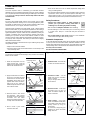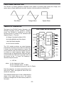
1
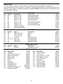
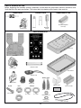
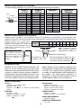
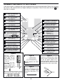
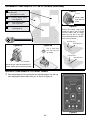
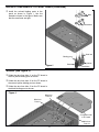
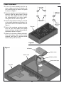
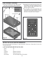
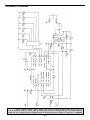
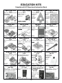
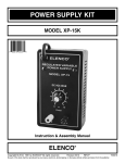
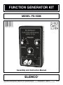
FUNCTION GENERATOR KIT MODEL FG-500K Assembly and Instruction Manual ELENCO ® Copyright © 2013 by Elenco® Electronics, Inc. All rights reserved. Revised 2013 REV-G No part of this book shall be reproduced by any means; electronic, photocopying, or otherwise without written permission from the publisher. 753069 PARTS LIST If you are a student, and any parts are missing or damaged, please see instructor or bookstore. If you purchased this kit from a distributor, catalog, etc., please contact ELENCO® (address/phone/e-mail is at the back of this manual) for additional assistance, if needed. DO NOT contact your place of purchase as they will not be able to help you. RESISTORS Qty. r 1 r 1 r 1 r 1 r 1 r 1 r 1 r 1 r 1 Symbol R6 R1 R5 R7 R8 R4 R9 R2 R3 Description 200Ω 5% ¼W 620Ω 5% ¼W 3.9kΩ 5% ¼W 8.2kΩ 5% ¼W 10kΩ 5% ¼W 22kΩ 5% ¼W 100kΩ 5% ¼W 10kΩ Potentiometer 100kΩ Potentiometer Qty. r 1 r 1 r 1 r 1 r 3 r 1 r 1 Symbol C6 C5 C4 C3 C2, C7, C8 C1 C9 Value 820pF (821) 10% .01µF (103) 10% .1µF (104) 10% 1µF 50V 10µF 16V 100µF 16V 1,000µF 16V Color Code red-black-brown-gold blue-red-brown-gold orange-white-red-gold gray-red-red-gold brown-black-orange-gold red-red-orange-gold brown-black-yellow-gold Part # 132000 136200 143900 148200 151000 152200 161000 192531 192612 CAPACITORS Description Discap Mylar Mylar Electrolytic (Lytic) Electrolytic (Lytic) Electrolytic (Lytic) Electrolytic (Lytic) Part # 228210 240119 251017 261047 271045 281044 291044 SEMICONDUCTORS Qty. r 1 Symbol U1 Value XR-2206 Description Integrated circuit (IC) Part # 332206 MISCELLANEOUS Qty. r 1 r 2 r 1 r 1 r 1 r 3 r 1 r 1 r 1 r 3 r 3 r 2 Description PC board DPDT switch PC mount Switch rotary 2p6pos Battery snap Battery holder Knob Case top Case bottom Binding post black Nut binding post Lockwasher binding post Binding post yellow Part # 511003 541009 542207 590098 590099 622009 623061 623062 625031 625031HN 625031LW 625034 Qty. r 4 r 3 r 1 r 2 r 1 r 4 r 1 r 1 r 1” r 9” r 1 -1- Description Screw 2.8 x 8mm Hex nut 7mm Hex switch nut 9 x 15mm Flat washer 8 x 14mm Flat washer 9mm Rubber foot 16-pin IC socket Label top panel Double-sided tape Black wire 22ga. Lead-free solder Part # 641102 644101 644102 645101 645103 662015 664016 721008 740020 814120 9LF99 PARTS VERIFICATION Before beginning the assembly process, familiarize yourself with the components and this instruction book. Verify that all of the parts are present. This is best done by checking off the parts in the parts list. RESISTORS CAPACITORS SEMICONDUCTOR Mylar XR-2206 Integrated circuit (IC) Carbon film Electrolytic (radial) Discap Potentiometer MISCELLANEOUS Case top PC board Label Lead-free solder Rotary switch Case bottom Battery snap Binding posts DPDT switch Screws Knob Nuts Rubber foot Battery holder Washers Black 16-pin IC socket Yellow Double-sided tape 2.8 x 8mm 7mm Flat 8 x 14mm Flat 9 x 15mm Binding post nut Binding post lockwasher 9mm -2- Black wire 22ga. IDENTIFYING RESISTOR VALUES Use the following information as a guide in properly identifying the value of resistors. BAND 1 1st Digit Bands 1 2 Multiplier Tolerance Color Black Brown Red Orange Yellow Green Blue Violet Gray White Digit 0 1 2 3 4 5 6 7 8 9 Multiplier BAND 2 2nd Digit Color Black Brown Red Orange Yellow Green Blue Violet Gray White Resistance Tolerance Color Multiplier Black 1 Brown 10 Red 100 Orange 1,000 Yellow 10,000 Green 100,000 Blue 1,000,000 Silver 0.01 Gold 0.1 Digit 0 1 2 3 4 5 6 7 8 9 Color Silver Gold Brown Red Orange Green Blue Violet Tolerance +10% +5% +1% +2% +3% +.5% +.25% +.1% IDENTIFYING CAPACITOR VALUES Capacitors will be identified by their capacitance value in pF (picofarads), nF (nanofarads) or µF (microfarads). Most capacitors will have their actual value printed on them. Some capacitors may have their value printed in the following manner. Electrolytic capacitors have a positive and a negative electrode. The negative lead is indicated on the packaging by a stripe with minus signs and possibly arrowheads. Also, the negative lead of a radial electrolytic is shorter than the positive one. Warning: Multiplier For the No. 0 1 2 3 Multiply By 1 10 100 1k Second digit First digit If the capacitor is connected with incorrect polarity, it may heat up and either leak, or cause the capacitor to explode. Polarity marking (–) Multiplier 103K 100V Tolerance* 4 5 8 10k 100k .01 9 0.1 Note: The letter “R” may be used at times to signify a decimal point; as in 3R3 = 3.3 Maximum working voltage The value is 10 x 1,000 = 10,000pF or .01µF 100V (+) * The letter M indicates a tolerance of +20% The letter K indicates a tolerance of +10% The letter J indicates a tolerance of +5% INTRODUCTION Assembly of your FG-500 Function Generator will prove to be an exciting project and give much satisfication and personal achievement. The FG-500 contains a complete function generator capable of producing sine, square and triangle wave forms. The frequency of this generator can be contiuously varied from 1Hz to 1MHz in 6 steps. A fine frequency control makes selection of any frequency in between easy. The amplitude of the wave forms are adjustable from 0 to 3Vpp. This complete function generator system is suitable for experimentation and applications by the student. The entire function generator is comprised of a single XR-2206 monolithic IC and a limited number of passive circuit components. SPECIFICATIONS OUTPUT: SQUARE WAVE: • Waveforms: Sine, Triangle, Square • Impedance: 600Ω + 10%. • Frequency: 1Hz - 1MHz in 6 decade steps with variable ranges. • Amplitude: 8V (no load) • Rise time: Less than 50ns (at 1kHz) • Fall time: Less than 30ns (at 1kHz) • Symmetry: Less than 5% (at 1kHz) TRIANGLE WAVE: SINE WAVE: • Amplitude: 0 - 3Vpp • Linearity: Less than 1% (up to 100kHz) • Amplitude: 0 - 3Vpp • Distortion: Less than 1% (at 1kHz) • Flatness: +0.05dB 1Hz - 100kHz POWER REQUIREMENTS: • Standard 9V battery OPERATING TEMPERATURE: • 0OC to 50OC -3- CONSTRUCTION ● Turn off iron when not in use or reduce temperature setting when using a soldering station. Introduction The most important factor in assembling your FG-500K Function Generator Kit is good soldering techniques. Using the proper soldering iron is of prime importance. A small pencil type soldering iron of 25 watts is recommended. The tip of the iron must be kept clean at all times and well-tinned. ● Tips should be cleaned frequently to remove oxidation before it becomes impossible to remove. Use Dry Tip Cleaner (Elenco® #SH-1025) or Tip Cleaner (Elenco® #TTC1). If you use a sponge to clean your tip, then use distilled water (tap water has impurities that accelerate corrosion). Solder Safety Procedures For many years leaded solder was the most common type of solder used by the electronics industry, but it is now being replaced by leadfree solder for health reasons. This kit contains lead-free solder, which contains 99.3% tin, 0.7% copper, and has a rosin-flux core. ● Always wear safety glasses or safety goggles to protect your eyes when working with tools or soldering iron, and during all phases of testing. ● Be sure there is adequate ventilation when soldering. Lead-free solder is different from lead solder: It has a higher melting point than lead solder, so you need higher temperature for the solder to flow properly. Recommended tip temperature is approximately 700OF; higher temperatures improve solder flow but accelerate tip decay. An increase in soldering time may be required to achieve good results. Soldering iron tips wear out faster since lead-free solders are more corrosive and the higher soldering temperatures accelerate corrosion, so proper tip care is important. The solder joint finish will look slightly duller with lead-free solders. ● Locate soldering iron in an area where you do not have to go around it or reach over it. Keep it in a safe area away from the reach of children. ● Do not hold solder in your mouth. Solder is a toxic substance. Wash hands thoroughly after handling solder. Assemble Components In all of the following assembly steps, the components must be installed on the top side of the PC board unless otherwise indicated. The top legend shows where each component goes. The leads pass through the corresponding holes in the board and are soldered on the foil side. Use only rosin core solder. Use these procedures to increase the life of your soldering iron tip when using lead-free solder: ● Keep the iron tinned at all times. ● Use the correct tip size for best heat transfer. The conical tip is the most commonly used. DO NOT USE ACID CORE SOLDER! What Good Soldering Looks Like Types of Poor Soldering Connections A good solder connection should be bright, shiny, smooth, and uniformly flowed over all surfaces. Soldering Iron 1. Solder all components from the copper foil side only. Push the soldering iron tip against both the lead and the circuit board foil. Rosin Component Lead 1. Insufficient heat - the solder will not flow onto the lead as shown. Foil Soldering iron positioned incorrectly. Circuit Board 2. Apply a small amount of solder to the iron tip. This allows the heat to leave the iron and onto the foil. Immediately apply solder to the opposite side of the connection, away from the iron. Allow the heated component and the circuit foil to melt the solder. 3. Allow the solder to flow around the connection. Then, remove the solder and the iron and let the connection cool. The solder should have flowed smoothly and not lump around the wire lead. Soldering Iron 2. Insufficient solder - let the solder flow over the connection until it is covered. Use just enough solder to cover the connection. Solder Foil Solder Gap Component Lead Solder 3. Excessive solder - could make connections that you did not intend to between adjacent foil areas or terminals. Soldering Iron Solder Foil 4. Solder bridges - occur when solder runs between circuit paths and creates a short circuit. This is usually caused by using too much solder. To correct this, simply drag your soldering iron across the solder bridge as shown. 4. Here is what a good solder connection looks like. -4- Soldering Iron Foil Drag ASSEMBLE COMPONENTS TO THE PC BOARD Care must be given to identifying the proper components and in good soldering habits. Refer to the soldering tips section in this manual before you begin installing the components. Place a check mark in the box after each step is complete. C1 - 100µF 16V Electrolytic (see Figure A) C2 - 10µF 16V Electrolytic (see Figure A) C3 - 1µF 50V Electrolytic (see Figure A) R9 - 100kΩ 5% ¼W Resistor (brown-black-yellow-gold) C4 - .1µF 10% Mylar (104) (see Figure B) R1 - 620Ω 5% ¼W Resistor (blue-red-brown-gold) C6 - 820pF 10% Discap (821) J1 - 4” Black wire 22ga. J3 - 2½” Black wire 22ga. (see Figure C) C5 - .01µF 10% Mylar (103) (see Figure B) U1 - 16-pin IC socket U1 - XR-2206 IC (see Figure D) J7, J8 - Jumper wire (use a discarded lead) PC board R6 - 200Ω 5% ¼W Resistor (red-black-brown-gold) C9 - 1000µF 16V Electrolytic (see Figure A) S2 - Slide Switch DPDT S3 - Slide Switch DPDT R4 - 22kΩ 5% ¼W Resistor (red-red-orange-gold) R7 - 8.2kΩ 5% ¼W Resistor (gray-red-red-gold) C7 - 10µF 16V Electrolytic (see Figure A) R8 - 10kΩ 5% ¼W Resistor (brown-black-orange-gold) C8 - 10µF 16V Electrolytic (see Figure A) R5 - 3.9kΩ 5% ¼W Resistor (orange-white-red-gold) J2 - 2½” Black wire 22ga. (see Figure C) Figure A Electrolytic capacitors have polarity. Be sure to mount them with the short negative (–) lead (marked on side) in the correct hole. Warning: If the capacitor is connected with incorrect polarity, it may heat up and either leak or cause the capacitor to explode. (–) (+) Mount the electrolytics horizontal to the PC board. Bend the leads at right angles and then insert the leads into the PC board. Figure B Figure D Bend the capacitor over before soldering. Insert the IC socket into the PC board with the notch in the direction shown on the top legend. Solder the IC socket into place. Insert the IC into the socket with the notch in the same direction as the notch on the socket. Figure C Cut one 4” and two 2½” wires and strip ¼” of insulation off of both ends of the wires. Solder these wires to the points J1, J2, and J3. or -5- Notch ASSEMBLE COMPONENTS TO THE PC BOARD (continued) Figure F R2 - 10kΩ Potentiometer Hex Nut 7mm (see Figures Ea & Eb) Cut off tab S1 - 6 position Rotary switch (see Figure F) Mount down flush with PC board. R3 - 100kΩ Potentiometer (see Figure Ea) Figure G Battery snap (see Figure G) Thread the battery snap wires through the hole in the PC board from the solder side as shown. Solder the red wire to the BT+ point and the black wire to the BT– point on the PC board. Red Wire (BT+) Black Wire (BT–) Figure Ea Figure Eb Put a 7mm hex nut onto the pot as shown. Red Wire (BT+) Black Wire (BT–) Cut off tab Mount the pot down flush with the PC board. Solder and cut off excess leads. INSTALL COMPONENTS TO FRONT PANEL r Peel the backing off of the front label and carefully adhere it to the top case, aligning the holes while doing so, as shown in Figure H. Figure H -6- INSTALL COMPONENTS TO FRONT PANEL (continued) r Install the colored binding posts to the panel as shown in Figure I. Use the hardware shown in the figure. Make sure that the small nuts are tight. Nuts Lockwashers Small nut Binding post Black Figure I Yellow Yellow WIRING (See Figure J) r Solder the wire from hole J1 on the PC board to the first yellow binding post as shown. r Solder the wire from hole J2 on the PC board to the second yellow binding post as shown. r Solder the wire from hole J3 on the PC board to the black binding post as shown. Figure J Wire from Point J2 Wire from Point J1 Component side of PC board Wire from Point J3 -7- FINAL ASSEMBLY r Fit the PC board assembly into the top case, making sure that all switches and pots come through the holes in the panel as shown in Figure K. 7mm Hex pot nuts 9mm Hex switch nut r Place the washers onto their locations as shown in Figure K, being careful to check the sizes. Then, tighten the hex nuts onto the potentiometers and rotary switch, noting their size as shown in Figure K. 8mm x 14mm Washers r Peel off the protective backing on one side of the double-sided tape and adhere it to the bottom case in the location shown in Figure L. Top case r Peel off the remaining protective backing from the tape and adhere the battery holder to the tape, with the battery holder in the direction shown in Figure L. 9mm x 15mm Flat washer r Obtain a 9 volt battery (alkaline preferred). Press the battery snap onto the battery terminals (see Figure L) and then mount the 9V battery onto the holder. Figure K Figure L 9V Battery Battery snap Bottom case Battery holder Double-sided tape Top case -8- FINAL ASSEMBLY (continued) r Remove the backing from each rubber foot and place them in the locations shown in Figure M. 2.8 x 8mm Screws r Assemble the top and bottom case sections and fasten with four 2.8 x 8mm self-tapping screws as shown in Figure M. Make sure the slots on the side line up with one another. Slot r Turn the shafts on the two potentiometers and rotary switch fully counter-clockwise. Push the three knobs onto the shafts so that the line on the knobs are on the points shown in Figure N. 2.8 x 8mm Screws Rubber feet Rubber feet Figure M Figure N TESTING THE FG-500 FUNCTION GENERATOR The unit may be tested by following the 4 steps listed below. Should any of these tests fail, refer to the Troubleshooting Guide. 1) SET THE SWITCHES AND POTS AS FOLLOWS: On/Off On Range 10 Frequency Maximum (clockwise) Amplitude Maximum (clockwise) Sine/Triangle Set Sine/Triangle switch to Sine position -9- 3) FREQUENCY CONTROLS In each of the following steps, start with the switch and pots as shown on the previous page. 6 range settings, vary the FREQUENCY pot from max to min and check that the frequency varies according to Table 1 on page 12. 2) OUTPUT WAVEFORMS Connect an oscilloscope probe to the square wave output. You should see about 8V peak to peak square wave of a little over 15Hz. Connect the oscilloscope probe to the sine/triangle wave output. You should see a sine wave of approximately 3V peak to peak or greater. Set the Sine/Triangle switch to the Triangle wave position. You should see a triangle waveform of approximately 3V peak to peak or greater. In both sine and triangle waves, the frequency is also a little over 15Hz. 4) AMPLITUDE CONTROLS Set the switch and pots as in Step 1. Connect the oscilloscope to the sine/triangle wave output and vary the AMPLITUDE pot. The sine wave amplitude should vary from near zero to approximately 3V peak to peak or greater. TROUBLESHOOTING GUIDE A) NO SINE/TRIANGLE OR SQUARE WAVE OUTPUT 1) Check the soldering on switch S3. 2) Check battery and battery snap. 3) Check the soldering on IC U1. 4) Check for +9V on IC1 pin 4. 5) Check that U1 is not installed backwards. 6) Check all of the values and soldering on R1, R2, R3, R4, R5, R7, R8, R9, C8, and C9. B) WRONG FREQUENCY ON ANY RANGE SETTING 1) This indicates a wrong value capacitor in the bad range position. C) SINE/TRIANGLE SWITCH DOESN’T WORK 1) Check the soldering on switch S2 and R6. 2) Check the value of R6. 3) Check pin 13 and 14 of U1. D) AMPLITUDE CONTROL DOESN’T WORK 1) Check the soldering on R3, R7, R8, R4 and R9. 2) Check the values of the above mentioned components. E) FREQUENCY CONTROL DOESN’T WORK 1) Check the soldering on R1 and R2. 2) Check the values of the above two resistors. -10- FUNCTIONAL DESCRIPTION The FG-500 is a function generator integrated circuit capable of producing high quality sine, triangle, and square waves of high stability and accuracy. A picture of each waveform is shown below: Sine Wave Triangle Wave Square Wave THEORY OF OPERATION The heart of the FG-500 Function Generator is the XR-2206 monolithic function generator integrated circuit. The XR-2206 is comprised of four main functional blocks as shown in the functional block diagram (Figure 1). They are: FUNCTIONAL BLOCK DIAGRAM AM Input • A Voltage Controlled Oscillator (VCO) Sine/Saw Output 2 Mult. Out 3 • An Analog Multiplier and Sine-shaper • Unity Gain Buffer Amplifier V+ • A set of current switches The VCO actually produces an output frequency proportional to an input current, which is produced by a resistor from the timing terminals to ground. The current switches route one of the currents to the VCO to produce an output frequency. Which timing pin current is used, is controlled by the FSK input (pin 9). In the FG-500, the FSK input is left open, thus only the resistor on pin 7 is used. The frequency is determined by this formula: 1 Timing Capacitor Timing Resistor 16 15 +1 Multiplier and Sine Shaper 4 13 5 6 7 8 Current Switches where fo is the frequency in Hertz R is the resistance at pin 7 in Ohms C is the capacitance across pin 5 and 6 in Farads Note that frequency is inversely proportional to the value of RC. That is, the higher the value of RC, the smaller the frequency. The resistance between pins 13 and 14 determine the shape of the output wave on pin 2. No resistor produces a triangle wave. A 200Ω resistor produces a sine wave. -11- Waveform Adjust 12 Ground 11 Sync Output 10 Bypass 9 FKS Input VCO Figure 1 fo = 1/RC Hz 14 Symmetry Adjust CONTROLS RANGE SWITCHES Six ranges of frequency are provided by the range switch as shown in Table 1. POSITION 1 2 3 4 5 6 TYPICAL FREQUENCY RANGE 1Hz - 15Hz 10Hz - 150Hz 100Hz - 1.5kHz 1kHz - 15kHz 10kHz - 150kHz 100kHz - 1MHz Table 1 SINE/TRIANGLE SWITCH ON/OFF SWITCH This SINE/TRIANGLE Switch selects the waveform, sine wave or triangle wave, sent to the SINE/TRIANGLE output terminal. The ON/OFF Switch turns the power to the FG-500 on or off. OUTPUT TERMINAL FREQUENCY MULTIPLIER The output marked SINE/TRIANGLE provides the sine and triangle waveforms. The output marked SQUARE WAVE provides the square wave. The output marked GND provides the ground for all output waveforms. The multiplier is a variable control allowing frequency settings between fixed ranges. The ranges are as shown in Table 1. AMPLITUDE CONTROL The Amplitude Control provides amplitude adjustment from near 0 to 3V or greater for both sine and triangle waveforms. QUIZ (answers on bottom of following page) 1) The heart of the FG-500 Function Generator is the _________ monolithic function generator integrated circuit. 7) The resistance between pins 13 and 14 determine the shape of the __________ wave on pin 2. 8) No resistor produces a __________ wave. 2) The XR-2206 is comprised of four main blocks. 9) A 200Ω resistor produces a ___________ wave. They are ____________________________, 10) The six ranges of frequency provided by the range switch are: ___________________, __________________, and ____________________. ________ to ________. 3) The VCO actually produces an output frequency proportional to an input ________________. ________ to ________. 4) The current switches route one of the currents to the VCO to produce an output __________. ________ to ________. 5) The frequency is determined by the formula _______________. ________ to ________. 6) Frequency is inversely proportional to the value of _____________. ________ to ________. ________ to ________. -12- -13Answers: 1) XR-2206; 2) A Voltage Controlled Oscillator, An Analog Multiplier and Sine Shaper, Unity Gain Buffer Amplifier and A Set of Current Switches; 3) Current; 4) Frequency; 5) 1/RC; 6) RC; 7) output; 8) triangle; 9) sine; 10) 1Hz to 15Hz, 10Hz to 150Hz, 100Hz to 1.5kHz, 1kHz - 15kHz, 10kHz - 150kHz, 100kHz - 1MHz. SCHEMATIC DIAGRAM EDUCATION KITS Complete with PC Board and Instruction Book Space War Gun 0-15V Power Supply Christmas Tree K-10 K-11 K-14 Rapid fire or single shot with 2 A low-cost way to flashing LEDs. supply voltage to electronic games, etc. Requires 9V battery 0-15VDC @ 300mA 8.5VAC @ 500mA LED Robot Blinker K-17 Produces flashing colored LEDs and three popular Christmas melodies. You’ll have fun displaying the PC board robot. Learn about free-running oscillators. Requires 9V battery Requires 9V battery Digital Bird Nerve Tester Yap Box K-19 K-20 K-22A Burglar Alarm K-23 You probably have never heard Test your ability to remain calm. This kit is a hit a bird sing this way before. Indicates failure by a lit LED or at parties. mild shock. Makes 6 exciting sounds. Alarm for your car, house, room, or closet. Requires 9V battery Requires 9V battery Requires 9V battery Requires 9V battery Whooper Alarm Metal Detector Pocket Dice FM Microphone K-24 K-26 K-28 AK-710/K-30 Can be used as a sounder or Find new money and old To be used with any game of Learn about microphones, siren. treasure. Get started in this chance. audio amplifiers, and RF fascinating hobby. oscillators. Range up to 100 feet. Requires 2 “AA” batteries Requires 9V battery Requires 9V battery Requires 9V battery Training course incl. Telephone Bug Sound Activated Switch Lie Detector K-35 K-36 K-44 Motion Detector AK-510 Our bug is only the size of a quarter, Clap and the light comes on . . . The sound will yet transmits both sides of a clap again and it goes off. tell if you are telephone lying. The conversation more you lie, to any FM the louder the radio. Use as a sentry, message minder, burglar alarm, or a room detector. No batteries required! Requires 9V battery sound gets. Two IC AM Radio AM-780K New design - easy-to-build, complete radio on a single PC board. Requires 9V battery. Requires 9V battery Requires 9V battery Transistor Tester Variable Voltage DC Auto-scan FM Radio Kit DT-100K FM-88K Power Supply Kit Unique design Test in-circuit transistors and - two-IC FM 0-15VDC diodes. receiver with training course. XP-15K Requires 9V battery Ideal for students, technicians, and hobbyists. Great for breadboarding. -14- Requires 9V battery ELENCO® 150 Carpenter Avenue Wheeling, IL 60090 (847) 541-3800 Website: www.elenco.com e-mail: [email protected]