1
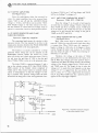
OPERATING INSTRUCTIONS
Type139B•A
PULSE
GENERATOR
-i
..,-<
m
__.
(,..)
'()
(X)
I
)>
G E N E R A
A
L
R A
D I 0
COMPANY
OPERATING INSTRUCTIONS
Type139B•A
PULSE
GENERATOR
Form 1398-0 lOOA
ID- 1032
March, 1966
Copyright 1966 by General Radio Company
West Concord, Massachusetts, USA
GENERAL
WEST
R A D I 0
CONCORD,
COMPANY
MASSACHUSETTS,
USA
TABLE OF CONTENTS
Section 1
INTRODUCTION . ..... .. .. .... .... . .... . ... . ...... .. . . . . .. . . . .
1.1
1.2
1.3
1.4
1.5
Section 2
INSTALLATION . . . . . . . . . . . . . . . . . . . . . . . . . . . . . . . . . . . . . . . . . . . . . . 5
2.1
2.2
2 .3
Section 3
Purpose ... . .. . .. . ....................... ... ...... . . . ... .
General Descr iption . .. .. . . . .. .. .. . ... . . . ... . ... . . . . .... . . .
Controls and Connectors . .... . ... .. . . ... ... ...... . ........ .
Accessor ies Supplied .. .. ....... .... . .. . . .... . .. . . . . .... . .
Accessories Avai Iable ........ . .... . .... . ... . . ... . . ...... .
Cooling . . . . . . . . . . . . . . . . . . . . . . . . . . . . . . . . . . . . . . . . . . . . . . . . . 5
Power Supply . . . . . . . . . . . . . . . . . . . . . . . . . . . . . . . . . . . . . . . . . . . . 5
Rack Mounting . . . . . . . . . . . . . . . . . . . . . . . . . . . . . . . . . . . . . . . . . . . 5
OPERATING PROCEDURE ...... . .... .. ... .... ...... . .. . ... .. . . 6
3.1 DefinitionofTerms . . . .... . . . ..... . . .... .. . .. .. .. . . .... .. . 6
3 .2
3.3
3.4
3.5
3.6
3.7
3.8
3.9
3. 10
3.11
3. 12
3.13
Section 4
Norma l Internal Operat ion .. . . . . . . . . . . . . . . . . . . . . . . . . . . . . . . . .
Normal Externa I Operat ion . . . . . . . . . . . . . . . . . . . . . . . . . . . . . . . . .
PRF vs Pulse Duration . . . . . . . . . . . . . . . . . . . . . . . . . . . . . . . . . . .
Precautions for Very Long or Very Short Pulses . . . . . . . . . . . . . .
Rise and Fall Times ... ....... . . .. .. . ...... ... .. . . . ... . . ..
External Load Considerations . .. ............ . .. .. ..... . ....
Output De Component - De Trans loti on . ... . ...... .. ..... . ..
Lock ing on High Frequency Signals .. .. ......... . . . .... . ....
Count-Down Operation . . ... .... ... .. . . . ...· . . . . . . . . . . . . . . . . .
Single-Pulse Operat ion .. ..... . .. .. . ... ... . . . . . ...... . . . . . .
Use as a Delay Generator . . .. . ... .. . . .... . .. .... ........ . . .
Use for Complex Waveforms ............ . . . . . .. . ... . . .. .. . ..
7
7
9
9
10
10
11
12
12
12
12
13
PRINCIPLES OF OPERATION . ..... . . . . ... ..... . ... . .... .. ... . 14
4. 1 General . . . ...... . ... . .. . .. .. ... ... . . . . . . .. . .. . . .. .... ... 14
4 .2 Input and PRF Osc illator C ircu it - External Operat ion . . ...... 14
4 .3 Input and PRF Osc illator Circuit- .Internal Operation . . ...... 15
4.4 Output Pulse and Timing Circu it s .............. . ... . ... ... .. 16
4.5
Section 5
Power Supply . . .. .. .... . . . ... . .. . . .... ..... . ........ . ... . 19
SERVICE AND MAINTENAN CE .... ....... . ....... . ..... . ...... 20
5.1
5 .2
5 .3
5 .4
5 .5
5.6
5 .7
5.8
Warranty ... .. . . ................. . . .. .... . ...... . . . ........
Serv ice .... . ...... . . . . . : . .. . ....... ." .. . .... . . . ..... . .....
Remove I of Cover .... . ......... . ....... . ........ .. ....... .
Routine Maintenance . . ... . ........ . ..... . ....... .. .. . . . ...
Trouble~Shoot i ng Notes . .. .... .. . . . .. ... . .............. . ...
Waveforms .. . .... . ...... . . . ......... . . . .... , .......... . ..
Voltages and Resistances ... .. ... . ........ . .......... . .. . .
Calibration Procedure ... . .. . . . .. . ...... . ...... .. . .. . . .... .
20
20
20
20
21
23
22
23
Parts Lists and Schematics ... ... .. . . . . ... . . . . ......... . . .. . .. . . .. ..... . .. 28
SPECIFICATIONS
PULSE REPETITION FREQUENCY
2.5 c/s to 1.2 Mc/s, with calibrated points
in a 1-3 sequence from 10 c/s to 300 kc/s, and 1.2 Mc/s, all ± 5%.
Continuous coverage with an uncalibrated control.
Internally Generated:
Aperiodic, de to 2.4 Mc/s with 1-V, rms,
input (0.5 V at 1 Mc/s and lower); input impedance at 0.5 V,
rms, approximately 100 kfl shunted by 50 pF. Output pulse is
started by negative-going input transition.
Externally Controlled:
~
0 UTP UT .pULSE CHARACTERISTICS
100 ns to 1 s in 7 decade ranges, ± 5% of reading or
±2% of full scale or ±35 ns, whichever is greater.
Duration:
Rise and Fall Times:
60 ns
Less than 5 ns into 50 or 100 fl; typically
+ 2 ns/pF external load capacitance into 1 kfl (60 V).
Voltage: Positive and negative 60-mA current pulses available
simultaneously. De coupled, de component negative with respect
to ground. 60 V, peak, into 1-kfl internal load impedance for
both negative and positive pulses. Output control has 10 steps
plus continuous adjustment.
Overshoot and noise in pulse, less than 10% of amplitude with correct termination.
Ramp-off: Less than 1 %.
1-IJ.S pulse into 50 ohms with
delayed sync pulse.
Delay-Sync Pulse: Consists of a negative-going transition of
approximately 5 V and 100-ns duration, coincident with the late
edge of the main pulse. Duration control reads time between
prepulse and delayed sync pulse. This negative transition is immediately followed by a positive transition of approximately 5 V
and 150 ns to reset the input circuits of a following pulse generator.
(See oscillogram.)
Stability: With external-drive terminals short-circuited, prf jitter
and pulse-duration jitter are each 0.04%. (Jitter figures may vary
somewhat with range switch settings, magnetic fields, etc.)
Power Required: 105 to 125, 195 to 235, or 210 to 250 V, 50 to
60 c/s, 90 W.
Overshoot:
Synchronizing Pulses:
Accessories Available:
MECHANICAL DATA
Positive and negative 8-V, approx, pulses of 150-ns
duration. If positive sync terminals are shorted, negative pulse
can be increased to approximately 50 V.
Prepulse:
Sync-pulse source impedance:
positive - approx 300 fl;
negative - approx 1 kfl.
TYPE l217-P2 Single-Pulse Trigger, rack-
adaptor panel.
Width
Convertible-Bench Cabinet.
Net
Weight
Shipping
Weight
in
kg
12
8. 5
INTRODUCTION
SECTION
1
INTRODUCTION
1.1 PURPOSE.
The Type 1398-A Pulse Generator is a general-purpose pulse source intended primarily for laboratory use. The repetition rates of the pulses may be
either internally controlled, at frequencies from 2.5 c/s
to 1.2 Mc / s, or externally controlled at frequencies up
to 2.4 Mc / s .
In addition to the main positive and negative output pulses, the instrument also supplies synchronizing
pulses that correspond to the beginning and end of the
main pulse. The early s ync pulse ( prepulse) is intended
chiefly for synchronizing an oscilloscope while the late
pulse (delay pulse) is intended to make the instrument
an accurate time-de lay generator.
1.2 GENERAL DESCRIPTION.
The Type 1398-A comprises three mam circuit
groups:
(1) A combination input circuit and oscillator tha t
establishes the repetition rate of the main pulse.
(2) A combination puls e-timing and output circuit
that establishes the duration and amplitude of the
main pulse.
(3) A power supply that provides regulated voltage
for the other two circuit groups.
The repetition frequency, duration, and amplitude
of the main output pulse are adjustable by front-pane 1
controls. The instrument, which is housed in a convertible-bench cabinet, may be used as supplied as a
bench instrument or may be quickly and easily adapted
for use in a relay-rack. (Refer to paragraph 2 .3.)
1.3 CONTROLS AND CONNECTORS.
See Figure 1-1 and Table 1-1 for the location and
the description of the controls and connectors used on
the Type 1398-A.
1.4 ACCESSORIES SUPPLIED.
One instruction book,form number 1398-0100.
One power cord, part number 4200-9622.
1.5 ACCESSORIES AVAILABLE.
Type 1217-P2 Single-Pulse Trigger , catalog number
121 7-9602. Used to generate single pulses . See Figure
1-2 and paragraph 3.11.4 for further details.
Type 480-P312 Relay-Rack Adaptor Set, c a talog
number 0480-9632. Us ed to rack-mount the Type 1398-A.
Refer to paragraph 2.3 for further details.
~TYPEl398-A PULSE GENERATOR
~--------------------------TABLE
1-l
CONTROLS AND CONNECTORS
Reference
(Figure 1-1)
Name
Function
1
PRF
12-position
rotary switch
Sets PRF range. In EXT
DRIVE, it changes prf
oscillator to an aperiodic
1nput circuit.
2
i',F
Continuous
rotary control
Adjusts prf continuously
between calibrated switch
positions. When set fully
clockwise, PRF switch is
calibrated. When PRF
switch is set to EXT DRIVE,
i',F control sets triggering
leve 1 of pulse generating
c1rcuits.
3
PULSE DURATION
Continuous
rotary dial
(no stop)
Sets pulse duration.
4
PULSE DURATION
RANGE
7 -position
rotary switch
Sets pulse duration range
in decade steps.
s
POWER OFF
Toggle switch
Turns instrument on and off.
6
OUTPUT PULSE -
Jack-top binding
post pair
For negative main output
pulse.
7
OUTPUT PULSE +
Jack-top binding
post pair
For positive main output
pulse.
8
AMPLITUDE
Inner Control
Continuous
rotary control
Adjusts amplitude
continuously between
switch positions.
10-position
rotary switch
Sets pulse amplitude
in ten steps from zero
to maximum.
Outer Switch
9
EXT OFFSET
Jack-top binding
post pair
(note shorting link)
For connection to an
external power supply
used to change de leve 1 of
of output.
10
SYNC DELAYED
Jack-top binding
post pair
For delayed sync pulse.
Amount o(delay is
controlled by PULSE
DURATION controls.
11
SYNC
For negative pre pulse.
12
SYNC+
Jack-top binding
post pair
Jack-top binding
post pair
13
EXT DRIVE
14
2
Type
For positive pre pulse.
Jack-top binding
post pair
For external drive signal.
12-terminal
female connector
For use with forthcoming
Type 1398-Pl DC Component
Control Unit.
INTRODUCTION
4
5
14
Figure 1-1. Type 1398-A Pulse Generator.
Figure 1-2. Type 12177 P2
Single·Pulse Trigger.
3
. . TYPE 1398-A PULSE GENERATOR
FRONT PANEL SCREW
--.......~
r/ )
FOOT SCREW
@..------A
Figure 2-1. Rock Mounting : Preparation
of instrument for attachment· of wings.
RUBBER FOOT
WING SCREW
~.
LOCKWASHER
f~-~f2k
CL/ p
/...
·~
NUT
Figure 2-2.
Rock Mounting : Wing assembly.
WING
Figure 2- 3. Rock Mounting : Attachment
of wings to instrument .
4
INSTALLATION
SECTION
2
INSTALLATION
2.1 COOLING.
It is important that the interior of the instrument
be adequately ventilated; therefore make sure the air
holes in the cover, especially those on the right side,
are not blocked.
2.2 POWER SUPPLY.
Connect the pulse generator to a source of power
as indicated by the legend at the input socket at
the rear of the instrument, using the power cord provided. While normally connected for 115-volt operation,
the transformer input circuit is so arranged that one
can make the conversion from 115-volt co 215-volr
operation simply by throwing a switch located directly
below the input socket. To do chis, unscrew the two
clamp fastners on the back of the instrument and slide
off the dust cover. Flip the switch over so that the
white indicator is on the 195- 235-volt side. The circuit
can also be adapted to accommodate a 230-volt line .
To do this, set the line voltage switch to the 195- to
235-volt position, and remove the two wires from terminal 2L, which is on the same panel as the line voltage switch, and connect them to terminal 2. For instruments changed to 215-volt or 230-volt operation, name-
plates (Type LAP166E5 for 215-volt operation, Type
LAP166E2 for 230-volt operation) may be ordered from
General Radio.
2.3 RACK MOUNTING.
The pulse generat9r can be rack-mounted by
means of a Type 480-P312 Relay-Rack Adaptor Panel
Set (catalog number 0480Q9632 ). The adaptor panels
are finished in charcoal gray crackle paint to match the
front panel of the instrument and come complete with
the necessary hardware co mount the instrument in the
rack. To make the installation, proceed as follows:
(a.) Remove the rubber feet. Retain the screws.
(b.) Remove and retain the screws chat secure the
front panel to the aluminum end frames (see Figure
2-1).
(c.) Remove the spacers between the front panel and
the end frames.
(d.) Install two clips on each wing using lock washers and nuts provided (see Figure 2-2).
(e.) Attach the wings co the instrument with the front
panel screws removed in step b (see Figure 2-3 ).
(f.) The assembly is now ready to be rack-mounted
in a standard 19-inch relay rack.
5
~TYPE 1398-A PULSE GENERATOR
SECTION
3
OPERATING
3.1 DEFINITION OF TERMS.
main pulse .... .. .... .. . .... ..... The principal output of the instrument; available at the OUTPUT PULSE binding posts.
prepulse ........................ The positive or negative sync pulse supplied just before the
start of the main pulse; available at the SYNC +and SYNC binding posts .
delayed pulse . . .... ... ....... .. . The pulse coincident with the end of the main pulse; available
at the DELAYED SYNC binding posts.
internal operation. . . . . . . . . . . . . . . The mode where pulse repetition frequency !S determined by
the pulse generator itself and controlled by the PRF controls
on the front panel.
external operation . . . ........ .. .. The mode where pulse repetition frequency is determined by
an external s ignal source; the pulse generator generates
pulses only when triggered by signals applied to the EXT
DRIVE binding posts.
duty ratio ... . ....... ... . . .... ... The ratio of pulse "on" time to the total time of the period
established by the prf setting; duty ratio, in percent = prf x
duration x 100 .
6
OPERATING PROCEDURE
3.2 NORMAL INTERNAL OPERATION .
3.2.1 PRF ADJUSTMENT.
Pulse repetition frequency is adjusted by the
PRF controls (1 and 2, figure 1-1), over a range of
2.5 c/s to 1.2 Mc/s . The PRF switch is calibrated to
indicate prf correctly only when the 6 F control is fully
clockwise. When the 6F control is fully counterclockwise, the prf is lowered well below the next lower PRF
switch setting. The range of adjustment of the 6F control is more than enough to span any one of the ranges
set by the PRF switch and thus affords continuous
coverage of the prf range of 2.5 c/s to 1.2 Mc/s . It is
important to remember, however, that the only calibrated
frequencies are those indicated by the PRF switch
positions, and that these are accurate only when th·e 6 F
control is fully clockwise .
3.2 .2 PULSE-DURATION ADJUSTMENT .
Duration of the main pulse is adjusted by the
PULSE DURATION controls (3 a~d 4, Figure 1-1).
The RANGE switch (4) selects one of seven decade
ranges and the range selected is covered by the PULSE
DURATION dial (3). This control consists of a knob
linked by a slow-motion drive to a dial that is calibrated from 1 to 11 in tenths of a unit. The overlap beyond
the decade span ensures continuous coverage of all
durations.
3.2.3 AMPLITUDE ADJUSTMENT .
Amplitude of the main pulse 1s adjusted by the
large AMPLITUDE switch, which varies the amplitude
from zero to maximum in ten steps, and by the small
amplitude control (concentric with the switch) which
facilitates continuous adjustment between steps. The
positions of the larger switch corresponds to changes in
in output impedance in 100-ohm steps. Thus a setting of
five indicates that the output impedance is about 500
ohms. When both controls are fully clockwise, the amplitude is 60 volts and the output impedance 1s one
kilohm.
3.2.4 FAMILIARIZATION PROCEDURE.
The best way to become familiar with the pulse
generator is to connect it to an oscilloscope and watch
the pulse s themselves. The procedure is as follows:
a. Connect the OUTPUT PULSE + binding post to
the oscilloscope vertical input by means of open
leads or a probe.
b . Connect the SYNC +binding post to the oscilloscope s ync or trigger input.
c. Connect any of the ground binding posts to the
oscilloscope ground.
d . Be sure that the link across the EXT OFFSET
binding pos t is firmly connected to both posts.
e. Adjust the oscilloscope trigger controls to trigger
on the 8-volt, 100- ns, positive pre pulse of the Type
1398-A.
f. Set the oscilloscope sweep rate controls for a
2-ms/div sweep rate.
g. Set the oscilloscope vertical gain controls for
about 40 volts/em sensitivity.
h . Set the PRF switch to 1 kc/s .
i. Set the 6F control fully clockwise.
j. Set the PULSE DURATION dial to 5.
k. Set the PULSE DURATION RANGE switch to
100 f.LS-1 ms.
1. Set the AMPLITUDE control fully clockwise.
The oscilloscope should now display a 1-kc
square-wave from the pulse generator. Use the PULSE
DURATION dial to shorten and to lengthen the pulse and
then set the PULSE DURATION RANGE switch to the
next lower range Decrease the prf first by turning the 6F
control counterclockwise and then by setting the PRF
switch to the next lower position. Adjust the oscilloscope sweep rate control to keep both the pulse duration
and frequency under observation. To decrease pulse amplitude, turn the AMPLITUDE control counterclockwise.
If the oscilloscope has a de-coupled vertical amplifier, set it for de, disconnect the pulse, and establish the ground reference trace . Now reconnect the positive main pulse and vary its amplitude. Then move the
connector from the + OUTPUT PULSE to the - OUTPUT PULSE binding post and vary the amplitude again.
Note that the pulse contains a de component that is
negative with respect to ground. The positive pulse
starts from -60 volts and rises to ground during its
active interval. The negative pulse starts from ground
and falls to -60 volts during its active interval.
If, during any of the above procedures, the pulse
is defective or the pattern becomes confused, check to
make sure that the pulse duration has not been made
too long for the pulse repetition frequency and that an
oscilloscope with a dc·coupled vertical amplifier 1s
used to observe pulses of very long duration.
3.3 NORMAL EXTERNAL OPERATION.
3.3.1 DRIVING-SIGNAL REQUIREMENTS .
The Type 1398-A will produce externally triggered
pulse s at frequencies from de to 2.4 Mc/s. The driving
signal should be applied to the EXT DRIVE terminals,
and should be at least 0. 5 volt,rms, up to 500 kc / s and
at least 1 volt, rms, from 500 kc / s to 2.4 Mc / s. Excessive driving voltages at frequencies above 1.5 Mc/s
may overload the triggering circuits . If the unit fails to
trigger, reduce the driving voltage. With optimum driving
voltage the unit will trigger to frequencies typic a lly as
high as 2.5 Mc/s.
7
~TYPE 1398-A PULSE GENERATOR
0,6
Iv
0.5
)0
0.4
1
/
"'<t
w
'}-0.3
0
~
<t
w
n.
...,o.2
:..J
0
>
0.1
~
0
I kc/s
2
5
10
20
50
v
100
/
7
v
200
500
DRIVING SIGNAL FREQUENCY
I Mc/s
2
l tJ98·tl
Figure 3-1.
Typical sens itiv ity-vs-frequency characteristics.
3.3.2 EXTERNAL DRIVE PROCEDURE.
For external operation, set the PRF switch to
EXT DRIVE and apply the external driving signal to
the EXT DRIVE binding posts. The 6 F control now becomes a triggering level adjustment; the input circuits
are set for maximum sensitivity wpen this control is
centered.
The input circuit is de-coupled, and the pulse
generator will operate from pulses at any low frequency
desired. The input signal must therefore either be at a
de potential close to ground or be ac -coupled, with an
external blocking capacitor.
3.3.3 OPERATION WITH OSCILLOSCOPE .
To observe external operation on an oscilloscope
proceed as follows:
a. Set up the equipment to display a 1-kc square
wave, as described in paragraph 3.2.4, a to I.
b. Set the PRF switch to EXT DRIVE.
c. Connect an adjustable audio-frequency generator
to the EXT DRIVE binding posts and set the generator to produce a 1-kc s ignal of at least 1 volt, rms .
d. Center the 6 F control (now use d as a triggering
level control). The oscilloscope should displa y a
square wave as described in paragraph 3.2.4.
e. Decrease the frequenc y of the audio-frequency
generator. Note that the external generatgr controls
the prf of the Type 1398-A.
f. Reset the audio-frequenc y generator to 1 kc /s and
reduce its amplitude. When the Type 1398-A fails to
8
trigger, adjust the 6 F control until triggering i s reestablished. When no further adjustment of the 6 F
control will re-establish triggering, the triggering
threshold has been reached (this should be at about
0.3 volt, p-to-p, to 1 kc/s). A plot of typical sensitivity is given in Figure 3.1.
g. Reset the generator amplitude to 1 volt, rms. If
possible, display its output waveform and the T ype
1398-A output pulse s imultaneously on the oscilloscope.
h. Adjust the 6 F cbntrol and observe the s tarting
point of the pul se . Note that the 6 F control adjusts
the phase at which the pulse is formed, and that the
pulse always s tarts during the negative-going input
transition.
TABLE 3-1 - - - - - - - - ,
DURATION ACCURACY VS DUTY RATIO
Duty Ratio
A ccuracy
0 to 20%
±2% of full sca le with
with DURATION dial at 1 to 4.
±5% of reading
with DURATION dial at 5 to 10.
±3 5 ns with durations of
0. 1 to 0.7 J-Ls .
20 to 50%
± 10% of reading.
Over 50%
Inaccurate.
OPERATING
~-----------TABLE
3.4 PRF VS PULSE DURATION.
P R F Control Setting
(6F control fully clockwise)
10
30
100
300
1
3
10
30
100
300
3.4.2 DURATION LESS THAN 50% OF PERIOD.
The accuracy of the DURATION control settings
rs preserved if the duty ratio is 50% or less (pulse
duration is 50% or le ss of total time of period). Table
3-2 lists the 50%-of-period figures for each PRF control
setting.
3.4.3 DURATION GREATER THAN 50% OF PERIOD.
When the pulse occupies more than 50 percent of
the total period, the dial reading of duration is erroneous. This effect is due to insufficient recovery time
for the pulse-forming circuits but can be circumvented
by the reversal of the OUTPUT PULSE polarity.
For example: A 1· kc, 600 t-LS positive pulse is
desired. From Table 3-2 it can be seen that 600 t-LS
exceed the 500 t-LS maximum duration given for a PRF
control setting of 1 kc/s (actual duty ratio = 10 3 x 6 x
10 4 x 10 2 = 60% ). But, from Figure 3-2, it also can be
seen that a positive duration of 600 t-LS can be obtained
if connection is made to the ~OUTPUT PULSE binding
post rather than to the + OUTPUT PULSE binding post
and if the DURATION controls are set to 400 t-LS pulse
(total period minus 600 t-LS ). The duty ratio for a 1-kc,
400- t-LS pulse is 40%; therefore the DURATION control
accuracy is preserved.
3-2------------~
50%-0F-PERIOD FIGURES
3 .4.1 DUTY RATIO LIMITS DURATION ACCURACY.
There is no restriction on the duty ratio of the
Type 1398-A. (Duty ratio is the ratio of the pulse "on"
time to the total time of the period established by the
prf setting; duty ratio in percent c prf x duration x 1 00.)
Therefore, the PULSE DURATION controls may be
mistakenly set for a duration longer than the total
period (period is the reciprocal of prf ). The instrument
cannot be damaged by such settings, but the user may
be confused by the resulting oscilloscope display.
Refer to Table 3-1 for duration accuracy versus dutyratio specifications.
PROCEDURE
50% of Period (Durations inaccurate
for DURATION control settings
longer than those listed)
so
c/s
c/s
c/s
c/s
ms
17 ms
5 ms
1.7 ms
kc/s
kc/s
kc/s
kc/s
kc/s
kc/s
500
170
so
1.2 Mc/s
3.4.4
f.J-S
f.J-S
f.J-S
17
5
1.7
f.J-S
0.42
f.J-S
f.J-S
f.J-S
DURATION EQUAL TO PERIOD.
When the DURATION controls call for a pulse
exactly equal to the pulse period, the instrument fails
completely, and both duration and prf are indeterminate.
3.4.5 DURATION GREATER THAN PERIOD.
When the duration is set longer than the pulse
period, the pulse timing circuits will 11 count down 11 ,
producing one pulse for each 2, 3, 4, ... n input periods.
In general, the pulse duration will not be precisely
controllable due to lack of recovery time. However,
such frequency division may be useful in some applications and it should be remembered that the Type 1398-A
can be used as a frequency divider of arbitrary scale
by such operation.
3.5 PRECAUTIONS FOR VERY LONG
OR VERY SHORT PULSES.
3.5.1 GENERAL.
When pulses of very long or very short duration
are to be produced and observed, special attention must
+OUTPUT PULSE
(INACCURATE)
DURATION CONTROLS SET TO 600)JS
. DURATION INACCURATE BECAUSE DUTY RATIO EXCE EDS 50%
-OUTPUT PULSE
(ACCURATE)
-60V
~
[13'98-2 [
DURATION CONTROLS SET TO 400)JS
DURATION ACCURATE BECAUSE DUTY RATIO IS LESS THAN 50%
Figure 3-2.
Circumvention of 50% duty-ratio limitation at 1 kc/s
by reversal of OUTPUT PULSE polarity.
9
~TYPE
1398-A PULSE GENERATOR
be given to the equipment setup and interconnections.
Bandwidth consideration s are fundamental and oscilloscopes with the desired frequency response must be
chosen as indicators.
3.5.2 LONG PULSES- LOW-FREQUENCY RESPONSE.
An oscilloscope with a frequency response to de
is necessary to observe very long pulses. The lowfrequenc y cutoff of most oscilloscopes that do not have
de amplifiers is about 5 or 10 c/s, and these oscilloscopes will exhibit "ramp-off" effects with pulse durations over 10 milliseconds. (Ramp-off is the slope on
the flat top and bottom.) Almost any indicator ha s
adequate high-frequency respon s e for long-duration
p~lses becuase the "flats" are usually of more int erest
th an are the rapid rise and fall voltage transitions. The
T ype 1398-A uses a direct-coupled output system and
will not cause ramp-off at any duration.
3.5.3 SHORT PULSES-HIGH-FREQUENCY RESPONSE .
Faithful reproduction of very short pulses or of
the rapidly changing voltage of the leading or trailing
edge of such a pulse require s wide-bandwidth amplifier
and indicator systems. For example , when a pulse with
a rise time of 0.05 JLS is displayed on a n oscilloscope
whose amplifier has a rise ti!l).e of 0. 05 j.ls, the indicated rise time will be 0.07 JLS· F or a system with n
individual components of spec ified rise time , the equation for over-all rise time 1 is
T,=jT/+T/+ .·.... T/
(1)
The rise time of an a mplifier system, T,, is related to
the 3-dB bandwidth, B, by the equation (2), where the
factor of 0.35 should be used if the overs hoot is less
than 10 percent. 2
0.35
to
B
0.45
(2)
3.6 RISE AND FALLTIMES.
The Type 1398-A has very short nse and fall
times (typically 5 ns) of output current into the internal
1-kilohm loads and their associated stray capacitances.
The internal stray capacitances are about 40 pF, which
results in open-circuit rise and fall rimes of about 90 ns
across the internal 1-kilohm load. The rise and fall
times increase linearly with external capacitance and
and decrease linearly with external resis tance - the
final transition time is about 2.2 RC. The intrinsic rise
time can therefore be observed onlo/ if a resistance of
100ohms or less is connected across the output binding
posts. With an open-circuit connection, the Type 1398-A
output circuit is capacitance-limited, the voltage transition varies exponentially with rime, and no overshoot
is possible. Because of this important feature, the
Type 1398-A can be used to check almost any amplifier
system for overshoot- including any oscilloscope whose
input impedance is over 1 kilohm.
For further information on rise and fall rimes,
refer ro paragraph 3.7, below.
3.7 EXTERNAL LOAD CONSIDERATIONS.
The output circuits of the pulse generator are as
stable as possible for an instrument of such simplicity.
Some important point s to remember are:
(l) The output tube s act as current sources that
produce 60-mA pulses into a paralle 1 combination of
the AMPLITUDE control resistors and whatever external load is connected to the instrument.
(2) The pulses are direct-coupled ro rhe OUTPUT
PULSE binding posts and therefore contain a negative de component of 60 rnA.
OUTPUT
40·pF
INTERNAL
c
'
;~;
o
:
I
I k.O.
·t
6r
r
12-pF
~ X TERNAL
+~LOAD
I
With very short pulses, it is neces sary to take care in
the wiring of system components. Short, direct wires
should be used for both signal and ground paths if open
wiring is used, and coaxial cables should be terminated
properly. A common sign of an improperly connected
ground or of an inductive loop in the wiring is the presence of high-frequenc y ringing (damped os cillation) on
the pulse trans ition s.
1
Va lley, G. E., a nd Wa llma n, He nry, "Vacuum Tube Amplifier s , " Radiation Laboratory Series, Vol 18, McGraw-Hi ll ,
1948, p 77 .
2
Ibid, p 80.
10
---l=--
-=:-
II.J9B-.JI
Figure 3-3. Equivalent circuit for Type 1398-A
output system feeding high load i mpedonce.
Figure 3-3 s how s a n equivalent circuit for the
Type 1398-A output system as it appears when feeding
a high external load impedance (e.g. , a 12 ~pF, 10megohm oscillo scope probe). The pulses from this circuit will be capacitance-limited by the 50-ns RC time
constant, and a ri se time of about 100 ns re s ult s
(Figure 3-4c ). The appearance of a brief pulse at ourput settings of 0.6 volt and 6 volts is shown in Figure
3-4 a and b, respectively.
OPERATING PROCEDURE
0 .6 volt, pe-ck-to-peak, into 10
ohms ; 0. 1 ,us/ em.
6 volts, peok-to-peak, into 100
ohms; 0 .1 ,us/ em.
Figure 3-4.
Pulses from circuit of Figure 3-3.
Two important features should be noted from the
above: (1) the rise rime can be controlled with no termination and maximum output, by the addition of fixed
external capacitance according to the. equation
T, (ns)
=
+ Cexr)
2. 2 (40 pF
( 3)
and (2) the ultimate ri se time can be realized only by
termination of the instrument either externally by
placing a 50-.12 resistor across the output terminals, or
internally by setting the output impedance to 50 .12
(AMPLITUDE switch at 0.1, AMPLITUDE control centered), or both, as shown in Figure 3-5. Here the time
constant of the output circuit is about 1.5 ns , and the
fast rise and fall of the current pulse can be observed.
OUTPUT
+-somA
1
l
40-pF
I k!l
INTE~NAL ;T~
I
-3V
50.0.
l
-~
Figure 3-5 . Equivalent circuit for
achieving ultimate rise time.
In this connection, the transitions will typic a lly be
less than 5 ns. See Figure 3-6 for the t ypical appearance
of waveforms under q:rminated conditions.
3.8 OUTPUT DC COMPONENT-DC TRANSLATION.
In certain applications it ma y be desirable to
remove or to change the de component of the ma in output pulse. If it is nece ssary only t o remove th e de
3-volt,
5- ,u s
pulse;
termination.
Figure 3-6.
36 volts, peak-to-peak, int o
kilohm, 0.1 ,us/ em.
50-ohm
component , and if the pulses a re fairly s hort and the
circuit impedance s high, the desired result may be obtained simply by addition of an external coupling capacitor large enough to prevent ramp-off for the desired
pulse duration. If the above conditions do not hold, or
if it is neces s ary to introduce de offset, an external
power supply can be connected to the OFFSET terminal. Such a connection will allow the de component
level to be shifted by as much as 20 volts in either the
positive or the negative direction since the voltage of
power supply is then applied to the plate load re s istor s
of the output tubes, rhus changing their quiescentvoltage levels.
The AMPLITUDE control is adjusted until a 20volr swing is attained as measured on an oscilloscope .
Then a n adjustable positive power s upply is connected
to the EXT OFFSET terminal and its voltage i s adjusted until the de output of the pulse generator is zero as
measured on a de voltmeter. Alternatively, th e voltages
needed for the desired offset may be precalculated and
set accordingly. For instance, if the duty ratio (refer to
paragraph 3.4. 1) is 50%, the required offset voltage is
+ 10 volts for a twenty-volt pulse . A + 10-volt power
s upply is connected to the EXT OFFSET terminal and,
us ing only a de voltmeter, the AMPLITUDE control adjusted so that the de le ve l is zero.
NOTE
Do not apply more than ± 20 volts to the
EXT OFFSET terminal, as voltages exceeding this level may damage the output
rubes.
As in (a), but with open-circuit termination 1 60-volt pulse.
Typical waveforms und er terminated conditions.
11
. . TYPE 1398-A PULSE GENERATOR
3.9 LOCKING ON HIGH FREQUENCY SIGNALS.
3.9.1
FREQUENCY DIVIDER ACTION.
If an external signal is applied to the EXT DRNE
binding posts and the PRF switch is set to one of the
numbered positions, the internal oscillator of the Type
1398-A will lock on the external signal. For instance,
if a 50-kc signal is applied at the EXT DRNE terminals and the PRF is set to nearly 10 kc/s the main pulse
of the Type 1398-A can be locked at 'Is the external
frequency of 50 kc / s. In other words, the pulse generator is operating as a 5-to-1 frequency divider and
supplies one output pulse for every five input pulses.
The pulse generator can be phase-locked in this manner
to frequencies well above the maximum prf of the internal oscillator.
3.9.2 OBSERVATION WITH OSCILLOSCOPE.
To observe the above action, connect an oscilloscope and an audio-frequency generator to the Type
1398-A as described in paragraph 3.3.3. If possible,
observe the waveform of the external generator on the
oscilloscope , together with the Type 1398-A output.
Then proceed as follows
a. Set the PRF switch to 1 kc/s.
b. Set the L F control fully clockwise.
c. Set the external generator to 1 kc/s .
d . Set the output amplitude of the external generator
to minimum and then increase it until the Type
1398-A locks.
e. Set the frequency of the external generator to
2 kc/s, 3 kc/s, 4 kc/s, etc., and each time advance
the signal amplitude to lock the pulse generator. In
this way the pulse generator can be locked at very
high ratios.
3.10 COUNT-DOWN OPERATION.
When the duration is set longer than the pulse
period, the pulse timing circuits will " count down",
producing one pulse for each 2,3,4, ... n input periods.
In general, the pulse duration will not be precisely
controllable, owing to lack of recovery time.
3.11 SINGLE-PULSE OPERATION.
3.11.1 METHODS.
There are three ways by which one can produce a
sing le pulse :
(1.) By rotating the 6 F control with the PRF switch
set to EXT DRIVE.
12
(2.) By touching the EXT DRNE binding post.
(3 .) By using the Type 1217-P2 Single-Pulse Trigger.
The following
method in detail.
three paragraphs explain each
3.11.2 ROTATION OF 6 F CONTROL.
Set the PRF switch to EXT DRIVE and rotate the
6 F control about 20 or 30 degrees clockwise from it s
center position and then reverse the direction of rotation. An output pulse will be produced as the 6 F con trol is moved counterclockwise past the center position .
Very little rotation is necessary to reset and to start the
input circuits. Be careful not to touch the EXT DRIVE
binding post because a pulse burst may be produced by
the injected hum .
3.11.3 TOUCHING EXT DRIVE BINDING POST.
Set the PRF switch to EXT DRNE and set the
L F control near the center of its range . A single pulse
will be produced when the EXT DRNE binding post is
touched. This method is useful only for very long pulses
because the driving signal is a burst of noise or hum.
3.11.4 TYPE 1217-P2 SINGLE-PULSE TRIGGER.
The most convenient way to produce single pulse s
is to use a pushbutton actuating-circuit such as the
T ype 1217-P2 Single-Pulse Trigger, shown pictorially
in Figure 1-2 and schematically in Figure 3-7. To use
it, set the PRF switch to EXT DRIVE and set the 6 F
control between three cquarters clockwise and fully
clockwise.
1.5V
P~~398-A
T+
I
I O.l~i:Ff
I
NORMALLY OPEN
0.1
XTERNAL
Ff
DRIVE
~~
TERMINAL
l
=
IIJ98-5l
Figure 3-7. Schematic diagram of the
Type 1217-P2 Single - Pulse Trigger.
To produce a main pulse when the switch opens,
connect the negative banana plug of the Type 1217-P2
(arrowhead terminal in Figure 3-7) to the EXT DRNE
binding post of the Type 1398-A.
To produce a main pulse when the s witch closes,
reverse the double banana plug of the Type 1217-P2 so
the positive banana plug (ground symbol in Figure 3-7)
is connected to the EXT DRIVE binding post of the
Type 1398-A.
3.12 USE AS A DELAY GENERATOR.
The delayed sync pulse from the Type 1398-A
can be used to operate the input circuits of a second
Type 1398-A with a minimum of adjustment. The delayed
OPERATING PROCEDURE
pulse cons 1s ts of a negative-going trans1t1on of about
5 vo lt s and 100-n s duration, followed immediately by a
pos itive transition of about 5 volt s and 150-ns duration.
The initial negative-going tra n s ition will trigger the
input circuits and start the main pulse of a following
T y pe 1398-A. The positive-going transition will then
re set the in put circuits of the second T ype 1398-A to
prepare it for the ne xt de layed pulse. Figure 3-8 shows
con ne c ti ons and timing waveforms of such a system.
3.13 USE FOR COMPLEX WAVEFORMS.
Since the output circuit of the Type 1398-A i s
essentially a current source feeding a resistive load,
the outputs of two or more pulse generators can be
directly_ paralleled to produce complex additive waveforms. The output impedance of n pulse generators so
paralleled is 1000/n ohms and the peak voltage is s till
60 volts. A complex waveform and the system to produce
it are shown in Figure 3-9.
TYPE 1398-A
PULSE GENERATOR,'~!' I
TYPE 12 10-C UNIT
R-C OSCI LLATOR
TYPE 1210-C
OUTPUT
TYPE 1398-A ,*II
PREPULSE
T YPE 1398-A,*I I
MAIN PULSE( NEG)
8
~~W~6 r~L~~ ----,1c~------~-------
TYP~ 1398-A, 112
_ _ _ _=F4-.-~
MAIN PULSE
ll._____
TYPE 1398-All3
Figure 3 - 8 .
Connection of two Type 1398 - A's
os a delay generator.
Figure 3-9 .
System for producing the complex waveform shown.
13
~TYPE 1398-A PULSE GENERATOR
SECTION
4
PRINCIPLES OF OPERATION
analysis of each circuit 1s contained m the following
paragraphs .
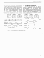
4.1 GENERAL. (See Figure 4-1.)
The T ype 1398-A is composed of three basic sections: (1) the input and prf oscillator circuit, (2) the
output pulse circuit, and (3) the power supply. The
first two sections are shown in block diagram form in
Figure 4-1.
4.2 INPUT AND PRF OSCILLATOR CIRCUITEXTERNAL OPERATION.
4.2.1 GENERAL.
Let us first consider the circuit as an a periodic
input circuit, i.e., with the PRF switch set to EXT
DRIVE, as shown in Figure 4-2. In this mode, the circ uit converts an external s ig nal , app lied t o the EXT
DRIVE binding pos t s, to a positive pulse , which appears at the output, pin 6 of VI 02.
Externally or internally ge nerated positive pulse s
from the input and prf oscillator circuit trigger the
output pulse circuit.
The output puls e circuit, in
turn, produces positive and negative pulses that appear at the OUTPUT PULSE binding posts. A detailed
INPUT AND PRF
r-oSCILLATOR CIRC~
r
OUTPUT PULSE CIRCUIT
I
r - - - - - - - - - - - o - - ' \ r D E L A Y E D SYNC
INT
AMPLITUDE
COMPARATOR
SC HMITT
VI04
SW EEP
GENERATOR
a CLAMP
v 1<.)3
r--'"";';';:;;<1 AMPLITUDE
EXT
DRIVE
START QI 0 3
QI02
l-'\loQv....-+0
F1_ POSITIVE OUTPUT
1---'~-o
L..JNEGATIVE OUTPUT
y
POSITIVE SYNC
NEGATIVE SYNC
Figure 4-l. Block diagram of the Type 1398- A Pulse Generator.
14
PRINCIPLES OF OPERATION
-VOLTAGE AMPLIFIER
[iR Fl
SIOI
Rl02
~r---
+150V
II
SCHMITT CIRCUIT--
+150V
T~MS:Nc
+150V
EXT
INT
.,__..__ __..
l~F I
TRIGGER
TO OUTPUT
PULSE CIRCUIT
VIOlA
Rll4
RI08
Figure 4-2. Simplified schematic diagram
of the input and prf oscillator circuit.
-150V
4.2.2 SCHMITT CIRCUIT .
Vl02A and B form a Schmitt trigger circuit.
Whether or not Vl02B is on (conducting) depends on
the voltage at the grid of Vl02A. When Vl02A's grid
voltage is considerably less then +50 volts, Vl02B
will be on. Vl02B's grid voltage is set at about +50
volts by Rll3 and R115. If the grid voltage of Vl02A
is raised toward +50 volts, i-t will begin to turn on . As
Vl02A goes on, its plate voltage will begin to fall,
lowering the grid voltage on Vl02B and lowering the
common cathode voltage . As the cathode voltage falls,
the plate current of Vl02A increases. This regenerative
action will terminate only when VI02B is completely
off and Vl02A completely on.
To turn Vl02B back on, the grid voltage of Vl02A
must be lowered to a level below that at which the
switching first took place. This voltage hysteresis
effect is shown in Figure 4.3. When Vl02B switches off,
its rapidly falling plate current produces the triggering
pulse, which is used to initiate the main pulse and
which serves as the pre-pulse for the SYNC terminals
after amplification by VlOlB. This pulse is produced
when Vl02A is turned on by a positive voltage applied
to its grid. The pre-pulse is therefore produced when a
negative transition occurs at the grid of VIOlA.
for maximum trigger sensitivity( centered), the quiescent
voltage at the grid of Vl02A will lie in the center of
the hysteresis region . Input signals applied to the EXT
DRIVE terminals are amplified by VIOlA and cause
Vl02 to switch. The exact phase at which the output
trigger will be formed is determined by the setting of
Rl03. Maximum sensitivity will be obtained when the
amplified signal is centered in the hysteresis region.
A single pulse can be produced (paragraph 3.4.2)
by rotation of the LIF control through its centered position. This rotation simply sets and resets the Schmitt
trigger .
4.3 INPUT AND PRF OSCILLATOR CIRCUITINTERNAL OPERATION.
4.3.1 GENERAL.
In Figure 4-2, the PRF switch is shown in the
EXT DRIVE position . When this switch is set to any of
the other positions, the voltage amplifier and Schmitt
circuits are converted to a prf oscillator.
4.2.3 QUIESCENT CONDITIONS.
In the absence of an input signal, the grid of
VIOlA will be at ground potential, and its plate voltage
will be around + 60 volts . Whether or not Vl02A will
be on will depend upon the setting of Rl03, the Ll F and
trigger-threshold control. When this control is adjusted
Figure 4-3. Diagram showing operation
of internal oscillator.
15
. . TYPE 1398-A PULSE GENERATOR
PRF:
0.01%
1:=:
-·
100 kc/s
1--~-
--
Figure 4-4a. Typical drift characteristics of prf oscillator.
5MIN
I~
=
11-
Figure 4-4b. Typical warmup characteristics of prf oscillator.
4.3.2 OSCILLATOR ACTION .
10.01 1
'"'"1
""'"""'"'·""'""'
1 11
"'·"'"· 1•
The PRF switch , SlOl, converts the input amplifier to a current source that translates the plate swing
of Vl02A so that it is symmetrical around its own grid
voltage . The switch ungrounds the junction of Rl07 and
RlOS and switches Rl02 from the plate supply voltage
to the plate of Vl02A . The l'IF control (R103) and R102
form the resistance part of the frequency determining
network and the PRF switch forms the capacitance part
by adding capacitance from the grid of V102A to ground.
The mechanism of oscillation is shown in Figure 4.3.
Suppose that V102A is off; its plate voltage is high and
C1 charges through R103 and R102 until V102A turns
on. When V102A turns on, its plate voltage falls and C1
begins to discharge. C1 continues to discharge until
V102A again turns off . The Schmitt circuit thus oscillates with V102A's grid voltage trapped within the
hysteresis region . The prf is changed by adjustment of
capacitance with the PRF switch and resistance with
the l'IF control.
9.9 -
1-
-
· ~==
9.8
=
97
· tlilllilililil!ll~l--l
9.5iiiiili=
~ 9.6
1;---
~
I~
1
~9.4
f----- rvO.I'%
~ 9.3
~9.2
'====
1
--==
_ _ _
9.1
90
·
r==
0
5
10
15
20
25
30
35
MINUTES FROM TURN-ON
i=
40
45
!t2!7-t3!
4.4.2 START AND STOP SIGNAL PATHS.
The output-pulse circuit requires a positive pulse
to start its action but, once started, will turn itself off.
Therefore, there are two signal paths in the circuit; one
to start the action and one to stop it. Both paths are
shown in Figure 4-5.
4.4.3 POWER AMPLIFIERS, AMPLITUDE CONTROL.
4.3.3 OSCILLATOR STABILITY .
The output frequency of this oscillator is quite
stable. Parameters important in controlling frequency
are R, C, and the magnitude of the hysteresis is established by the Schmitt circuit design, where both sections
of V102 operate farfrom zero bias so thatR114 provides
current feedback, and stabilizes the circuit against the
effects of changing tube characteristics. Typical warmup and drift characteristics are shown in Figure 4-4.
4.4 OUTPUT PULSE AND TIMING CIRCUITS.
4.4.1 GENERAL.
A balanced-output amplifier pair 1s driven by a
transistor flip-flop circuit to produce the output pulses.
The same transistor circuit activates the pulse timing
circuit comprising a ramp· generator ( V103) and a
Schmitt circuit (V104) used as an amplitude comparator.
16
The output power amplifiers are V105 and V106.
Nine 100-ohm resistors and one 120-ohm rheostat connected in series make up the plate-load resistance
of each amplifier. A single switch determines for both
amplifiers the output voltage by switching, in rheostat
fashion, the appropriate number of 100-ohm resistors
into the output circuit. The two 120-ohm rheostats are
ganged together to provide continuous .amplitude control, so that a common front panel AMPLITUDE control sets the output amplitude and impedance of both
amplifiers .
4.4.4 +OUTPUT AMPLIFIER.
Quiescent:Vl05 ON
With the AMPLITUDE control set for the maximum
output, the positive output puls'e starts from -60 volts
and rises to 0 volts. Therefore, in the quiescent state
(before the trigger pulse from the input and prf oscilla-
PRINCIPLES OF OPERATION
tor circuit is applied) VlOS is on (conducting) and
about 60 rnA flows through the output resistors.
4.4.7 TRIGGER AMPLIFIERS.
Start-Signal Action
4.4.5 -OUTPUT AMPLIFIER.
Quiescent: Vl06 OFF
Q103 and Q104 are the trigger amplifiers. Both
are biased off. Since both are npn transistors, a positive pulse applied to their bases will turn them on for
the duration of the pulse. When a start signal (positive
pulse) arrives from the input and prf circuit, it is
applied to the base of Q103. Ql03 conducts and produces a negative pulse at its collector.
The negative output pulse starts from 0 volts and
falls to -60 volts, Therefore, in the quiescent state,
V106 is off (not conducting) , no current flows through,
its plate load resistors and the -OUTPUT point rests
at ground potential ( 0 volts ).
4.4.6 MUL TIVIBRATOR DRIVER,
OUTPUT AMPLIFIER BIAS.
Quiescent: QlOl OFF, Ql02 ON
4.4.8 MUL TIVIBRATOR DRIVER SWITCHING.
Start-Signal Action
The plate voltages of the output amplifiers are
controlled by their grid voltages, which, in turn, are
controlled by the bistable driver, which consists of two
npn transistors, QlOl and Q102.
As noted before, VlOS is on in the quiescent state,
which means its grid bias must be low enough to allow
conduction . VlOS and V106 are self-biased by their
common cathode resistor R156, through which about
70 milliamperes flow for a 2-volt bias. If QlOl were
on (conducting), current wol,lld flow through R154, and
the voltage drop across R154 and R156 ( VlOS bias)
would be sufficiently large to turn off VlOS. Since VlOS
is on, QlOl must be off . When QlOl is off, Q102 is on
becaus~ the two transistors .form a bistable multivibrator.
With Q102 on, current flows through R157 to bias V106
off - the quiescent condition described above in paragraph 4.4.5.
AMPLITUDE ~
!cOMPARATOR
+150V
+15DV
SCH~~TT I
I
I
SWEEP GENERATOR
AND CLAMP
l
The negative pulse at the collector of Ql03 is
coupled to the base ot Ql02 and causes Q102 to start
to turn off. Q102 is one half of a multivibrator that consists of Q102 and QlOl; as Q102 starts to turn off,
QlOl starts to turn on. This is the normal regenerative
action of any multiv ibrator and the discussion that
follows describes the switching action and the regenerative paths of QlOl and Q102 .
The negative pulse at the base of Ql02 appears
as a positive pulse at the collector of Q102 . This positive pulse is coupled through C134 to the base of QlOl
and causes QlOl to start to turn on. The positive pulse
at the base of QlOl appears as a negative pulse at the
collector. This negative pulse is coupled through C133
and Rl39 back to the base of Q102, aids the negative
pulse already present from the collector of Q103, and
thus completes the regenerative loop. Upon completion
of the switching action, QlOl is on and Q102 is off.
I
SL...~-60
Figure 4-5. Simplified schematic
diagram of the output-pulse circuit.
~~-60
START
L
TRIGGER
AMPLIFIERS
AMPLITUDE
j
I MULTIVIBRATOR I
L.:.::.:: DRIVER ~
I ms -25 I
LPOWER AMPLIFIERS)
17
~TYPE 1398-A PULSE GENERATOR
4.4.9 OUTPUT AMPLIFIERS.
Start-Signal Action
As long as V103A is on, C will not charge, and Vl03B
will be on, holding C 's voltage to V.
Since the multivibrator driver has reversed its
state, the output amplifiers have also reversed their
states. VlOS is now off and the +OUTPUT PULSE
voltage is 0 volts, and VI06 is now on and the -OUTPUT PULSE voltage is -60 volts instead of 0 volts.
All that remains to convert these de-voltage steps to
pulses is to return the circuits to their quiescent levels .
4.4 .10 SWEEP GENERATOR AND CLAMP,
DURATION CONTROL.
Quiescent: V103A ON, V103B ON
The stop-signal path returns the circuits to their
quiescent levels. The time required to do this is the
output pulse duration; therefore the PULSE DURATION
controls are located in the stop signal path.
The duration is actually controlled by a sweep
generator whose sweep rate can be adjusted by the
DURATION controls. Before the arrival of a start
pulse all circuits are in their quiescent states. Vl05 is
on, and since the grid bias of Vl05 is also the grid
bias of Vl03A, Vl03A is also on in the quiescent state.
The diode Vl03B is connected between C and a
tap on the cathode resistor Rl25 (the PULSE DURATION control) of the Schmitt circuit comprised of
Vl04A and B. This resistor carries a constant current
(about 15 milliamperes) so that the voltage V at the
tap is constant. This positive voltage forms the base
from which the ramp pulse of the sweep generator rises.
4.4 . 11 AMPLITUDE COMPARATOR SCHMITT.
Quiescent: V104A OFF, V104B ON
Since the voltage V on its grid is held equal to
or lower than its cathode voltage , Vl04A is bia s ed off.
Since V104A and B are a Schmitt circuit, V104B must
be on if V104A is off. Vl04A will not turn on until the
voltage on its grid exceeds the voltage on the grid of
Vl04B set by R127 and R129.
4.4.12 SWEEP GENERATOR AND CLAMP.
Stop-Signal Action
When Vl05 reverts from its quiescent state, it
turns off. Vl03A also turns off because both tubes share
a common bias. When Vl03A turns off, capacitor C
begins to charge to +150 volts. As it charges, it draws
current through the plate load resistor, R, of Vl03A
and thus keeps the plate of Vl03A from returning immediately to + 150 volts.
Therefore, the voltage at the plate of Vl03A
goes positive at a rate determined by the value s of C
and R. When this voltage goes more positive than V,
Vl03B turns off. When the voltage reaches the switching
voltage of the Schmitt trigger-circuit, Vl 04A turn s on
and Vl04B turns off. The length of time it takes the
voltage on C to reach this level depends on the base
voltage V : if V is tapped from the top of Rl25 , the
time is short; if V is zero (tapped from the bottom),
time is long. When Vl04B turns off, a positive pulse is
applied to the stop-trigger amplifier.
R506
'--------o -150V REGULATED
Figure 4 - 6. Simplified schematic diagram
of the power-supply circuit.
18
PRINCIPLES OF OPERATION
4 .4 . 13 STOP-TRIGGER AMPLIFIER.
Stop-Signal Action
The stop-trigger amplifier behaves in the same
fashion as the start trigger amplifier when it receives
a positive pulse, i.e., it reverses the state of the multivibrator, which , in turn , reverses the state of the output
amplifiers. Thus V105 is turned back on, Vl06 is turned
off, all circuits have returned to their quiescent levels,
and the output pulse is terminated.
and R513 form a voltage divider establishing the grid
potential of amplifier tube V503 at a level very slightly
more negative than the cathode. The plate current of
V503 in R507 controls the drop across V501. V501 and
V503 are therefore an amplifier with high gain and any
attempt by V503's grid voltage to change with respect
to its cathode voltage results in a compensating change
in the voltage drop across V501. The drop across R513
and to the top of R512 is therefore held very constant
and is near 80 volts.
4.5 POWER SUPPLY. (Figure 4-6).
4.5.3 THE POSITIVE VOLT AGE SUPPLY .
4 .5 . 1 GENERAL.
The constant -150-volt source established with
V501B, V503, and V504 is used as a reference for the
positive supply. The plate current of V502, the cathode
of which is grounded, in R501 controls the drop across
V501A. Thus V501A and V502 comprise an amplifier
with high gain. The grid voltage of V502, only slightly
negative (one volt) with respect to it s cathode, is established by the vo ltage divider consisting of R504,
R505, and R506. This divider is set so that the portion
of resistance above the tap is equal to that below. For
the grid voltage of V501 to be near zero volts the output voltage at pin 3 of V501 must be 150 volts.
Both the positive and negative 150-volt supplies
are highly regulated with conventional amp lifier, seriestube, voltage regulators. The negative supply contains
the reference tube and is therefore the primary regulated
voltage source . The positive supply obtains its reference from the negative. The raw de spurce for each
supply is a full-wave bridge rectifier with a capacitor
inputfilter. CR501, CR502, CR503, and CR504 provide
+ 225 volts with respect to ground to the first half of
V501, the positive series tube . In similar fashion
CR505, CR506, CR507, and CR508 provide an equal de
voltage which divides across the second section of
V501 and the load to provide -150 volts regulated with
respect to ground.
4.5.2 THE NEGATIVE VOLTAGE SUPPLY.
R510 and V503 draw about 10 milliamperes of
current in V504, the voltage reference tube. The drop
across V504 is a very constant 80 volts. R511 , R512,
4.5.4 THE HEATER VOLTAGE SUPPLY.
Two heater busses are used in the Type 1398-A.
The 6.3-volt de heaters of VIOl, Vl02, Vl04, V501,
and V502 are fed from a common buss at ground potential. The heater supply for Vl03, Vl05, Vl06, and V501
is biased to - 70 volts de by a divider from - 150 volts
comprised of R514, R515, and R518.
19
. . TYPE 1398-A PULSE GENERATOR
SECTION
5
SERVICE AND MAINTENANCE
5.1 WARRANTY.
We warrant that each new instrument sold by us
is free from defects in material and workmanship and
that, properly used, it will perform in full accordance
with applicable specifications for a period of two years
after original shipment. Any instrument or component
that is found within the two-year period not to meet
these standards after examination by our factory, sales
engineering office, or authorized repair agency personnel will be repaired or, at our option, replaced without
charge, except for tube s or batterie s that have given
normal service.
5.2 SERVICE.
The two-year warranty stated above attests the
quality of materials and workmans hip in our products .
When difficulties do occur, our service engineers will
assist in any way possible. If the difficulty cannot be
eliminated by use of the following service instructions,
please write or phone our gervice Department (see rear
cover), giving full information of the trouble and of
steps taken to remedy it. Be sure to mention the serial
and type number of the instrument.
20
Before returning an instrument to General Radio
for service , please write to our Service Department or
nearest sales engineering office, requesting a Returned
Material Tag. Use of this tag will ensure proper handling and identification. For instruments not covered
by the warranty, a purchase order should be forwarded
to avoid unnecessary delay .
5.3 REMOVAL OF COVER.
To open the instrument for access to components,
loosen the large fluted screw at .the rear of the righthand side of the cabinet. Then grasp the panel by the
top and bottom edges with one hand, and with the other
hand slide the aluminum dust cover away from the panel
and off the rear.
All components are easily accessible. See Figures
5-3, 5-4, and 5-6 for location of components.
5.4 ROUTINE MAINTENANCE.
5.4.1
LUBRICATING THE FAN MOTOR.
For long , trouble-free operation, lubricate the fan
motor at least once a year with SAE 20 or 30 premiumqualit y oil. There are two lubricating holes, one in
SERVICE AND MAINTENANCE
each of the bras s brackets on either side of the motor
laminations.
5.4.2 CLEANING THE AIR FILTER.
To maintain proper cooling efficiency, the air
filter should be cleaned periodically. Local air conditions determine how often this is necessary . To clean,
release the air filter from its holder, rap gently to remove
excess dirt, flush from the dirty side with hot soapy
water, rinse, and let dry. Commercially available preparations to increase the filtering efficiency may be
applied but are not necessary.
5.5 TROUBLE-SHOOTING NOTES.
5.5.1 GENERAL .
If the pulse generator 1s inoperative, make the
following simple checks before proceeding further:
a . Check the power line voltage and frequency to
make sure they are as required by the power supply.
b. Check line cord, fuses , and power supply voltage.
If the voltage from pin 3 of V5 01 to ground is not
150 volts or if the voltage from pin 2 of V504 is not
-150 volts, refer to paragraph 5.5.2 .
c. See if the pre pulse is present at the SYNC binding
posts. If this pulse is present and the main pulse is
defect ive, refer to paragraph 5.5 .2 . If the pre pulse is
pre s ent and there is no main pulse, refer to paragraph
5.5 . 3. If neither prepulse nor main pulse is present,
refer to paragraph 5.5.4. If prepulse is absent and
the main puls e is present, refer to paragraph 5 . 5.7.
5.5.2 INOPERATIVE POWER SUPPLY.
Incorrect voltage. If the positive supply voltage
at pin 3 of V501 is regulated but not + 150 volts with
respect to ground, first see if the negative supply voltage at pin 4 of V504 is -150 volts. If this voltage is
regulated but not correct , adjust R512 so that an accurate voltmeter ind icates + 150 volts from pin 3 of
V501 to ground. If the positive supply voltage adjustment drifts, but the negative supply voltage does not,
replace either R504, R506 , or R505. If the negative
supply voltage adjustment drifts, replace R5ll, R513,
R510, R512, or V504 .
If the voltage drops only at full load, replace
VSOl, and check the voltage at pins 2 and 5 of V501.
If either of these voltages is less than 210 volts, check
the corresponding capacitors and diodes .
Unregulated voltage. The most probable cause of
thi s trouble is a defective tube. Remove V502 and V503
test them, and replace any defective tube. Measure the
voltage at pin 2 of V503 with respect to ground . If this
is not within 5% of -66 volts, regardless of the output
load , replace V504. Measure the resistances to ground
from pin 2, pin 3, pin 5, and pin 6 of V501 and compare
the results with the values in Table 5-l. Replace any
defective resistors or capacitors thus found.
No output supply voltage. Check V501. Measure
the regulator input voltage across C50l and C502. If
either of these voltages is zero, check for a shorted
rectifier diode, C501, C502 , and a blown fuse in the
primary of T501. If the input voltage is normal, check
V502 and V503 for an internal short . Check V504 for a
short. Measure the voltages at key points with a vacuum
tube voltmeter, comparing them with those given in
Table 5-l.
Incorrect heater voltage. If the de voltage at pin 4
of Vl03, Vl05 , or Vl06 or pin 3 of V503 is not within
10% of -70 volts, check for a cathode-heater short in
one of those tubes. Check the resistance to ground from
pin 2 of V504 against the value in Table 5-l. Replace
any defective resistors. Check for a short in C504 or
C505 .
5.5.3 DEFECTIVE MAIN PULSE .
Overshoot. Under normal conditions , with a high
impedance load, overshoot is not possible on any transition. Therefore, check the oscilloscope for overshoot
first. If overshoot occurs with a low-impedance terminated system, check the s y stem for proper grounding
and make sure that all wiring is as short as possible.
Note that some overshoot may be present on negative
pulse transitions as shown in Figure 3.6.
Large imbalance in pulse amplitudes or slowly
falling negative-going edge of positive pulse. These
defects can be caused by weakening of one of the output tubes.
Output pulse occasionally fails, and starts only
when RANGE switch setting is changed. There are two
possible causes of this difficulty: (1) The ionization
voltage of Vl07 has drifted sufficiently so that the
automatic restarting circuit no longer functions, or (2)
a tube has developed heater-to-cathode leakage. First
check the voltage from the negative side of V107 to
ground, using an electronic voltmeter of at least ~00
megohms input impedance. The proper voltage is -65
± 5 volts behind 5 megohms. If this voltage is correct,
the trouble is a defective Vl07, and a new NE-96 should
be installed . If the voltage measured is not correct,
check all tubes for heater-to-cathode leakage.
Pulse-duration errors. An error indication on only,
one setting of the RANGE switch is an indication that
a time~determining component for that range has drifted
or failed.
21
~ TYPE 1398-A
PULSE GENERATOR
5.7 VOLTAGES AND RESISTANCES.
TABLE 5-1
VOLTAGES AND RESISTANCES
**
De Volts
Tube
Pin
!:2.
Ground
VIOl
( 6DJ8)
1
2
3
6
7
8
1
Vl02
( 6DJ8) 2
3
6
7
8
34
- 0.1
0.8
145
0
4.5
***
Ohms
to
Ground
125
34
40
150
33
40
3.2k
lOOk
3.3k
2.5k
70k
3.3k
46
1
Vl03
( 6DJ8) 2 - 125
3 - 120
6
47
7
47
8
46
60k
4.6k
4.8k
5.5k
5.5k
60k
Transistor
(Type)
QlOl
( 2N2369)
Lead
E
B
c
Ql02
( 2N2369)
E
B
c
*
***
Ohms
to
Ground
1
2
3
6
7
8
150
46
54
150
52
54
1.6k
63k
5k
1.2k
65k
5k
V501
( 6080)
Vl05
( 8233 )
1
2
3
8
-70
- 122
0
- 125
lk
50k
0
49k
V502
(6AG5)
1
2
5
6
- 4.8
0
130
165
80k
0
1M
lOk
V106
( 8233 )
1
2
3
8
0
- 122
0
- 130
lk
50k
0
49k
V503
(6AH6)
V107
+
(NE-96) -
46
-65
63k
5M
1
2
5
6
7
- 68
-66
- 12
9.2
- 66
15k
27k
1M
8.5k
27k
V504
( 5651 )
1
2
- 66
- 150
Pin
Tube
33k
1M or lOk*
60k
lk
22k
lk
•••
**
De Volts
!2
Ground
Vl04
( 6922 )
De Volts
to
Supply
***
Ohms
to
Ground
1.9
2.1
24.5
1. 9
2. 9
2.2
**
De Volt s
Tube
Transistor
(T y pe)
Lead
24
50k
50k
Q103
( 2N2369)
E
B
24
50k
50k
Ql04
( 2N2369)
c
E
B
c
Pin
1
2
3
4
5
6
Ohm s
.l:_Q
I_Q
Ground
Ground
130
225
150
- 12
70
0
1M
De
Volts
-to
Supply
***
Ohms
to
Ground
0.96
0
2 .9
12
5.6k
50k
0.96
0
2. 1
12
5.6k
50k
0
1M
0
27k
0
Depends on ohmmeter polarity and res i stance range.
** All heater voltages = 6.2 volts ac.
*** Power supply disconnected, terminals #117 and #118 (near AMPLITUDE contro l ) grounded, all transistor s remov ed .
TEST CONDITIONS
Thi s ta b le li s t s importa nt voltages a nd res istances in th e Ty pe 1398-A.
The s e v ol t a ges, mea s ured by a Type 1806-A E le c troni c Vo ltmete r (i n put res ist ances = 100 MD), are accu ra te to wit h in ±5%. R5 05 a nd R5 12 we re set for
no rmal power s u pp ly out put =150 vol ts d e . Power line =1 15 vo lt s , power = 82
wat ts . The T ype 13 98-A c ontro ls were set as foll ows:
PRF .. . .. ... . . . ... ..... . .... .. .. .... . 1 kc /s
M . . . . . . . . . .... ..... . ... .. . . ...... centered
PULSE DURATION
dial . .. . .. . ... . ..... .. . . . . . . .. 1
RANGE .... . .. ... . . .. 0. 1 to 1 ps
AMPLIT UDE ..... ... . . . . .. . . . ... 10 (fully cw)
22
SERVICE AND MAINTENANCE
A uniform error on all range s is an indication that
the amp litude compari s on circuit (Vl04 and as s ociat e d
components) is defective. For in s tance, a decrea s e in
re s istance of Rl27 would make all pulses too long a t
all s ettings of the PULSE DURATION controls , while
an increase in this re s i s tance would reverse the effe c t.
If the output puls e is of fixed , long duration ,
independent of the PULSE DURATION controls, Vl03B
is not functioning a nd a new tube s hould be in s erted.
Another difficult y tra c e able t o a defecti ve Vl03
would be excessive duration at th e high end of each
range, especially at longer duration ranges. It i s probable that V 103 is not remaining off, and it should be
replaced.
5.6 WAVEFORMS.
5.6.1 TEST CONDITIONS .
Figure 5-l depicts important waveforms in t he
Type 1398-A . They we re taken with a 10-megoh m, 12-pF
probe; the vertical s en s itivity listed beside each os s c illogram include s the 10 X attenuation of the probe.
The T ype 1398-A c ontrols were se t as follows (except
where noted ):
PRF .
100 kc / s
6 F.
centered
PULSE DURATION dial
.. .1
PULSE DURATION RANGE ... . 0.1 to 1 ,u. s
AMPLITUDE.
. ...... 10 (fully clockwise)
Vl02, pin 1,
20V / em, 2 /ls/ em .
Vl02, pin 2,
20V/ em, 211s/ em .
5.5.4 NO MAIN OUTPUT PULSE, SYNC PULSES
PRESENT .
If no output puls e s are pre s ent and Vl07 fla s he s
continua lly, c heck Vl0 3 and Vl04 and replace if ne c e s sary .
If Vl07 is not fla s hing, measure the voltage at
the +OUTPUT PULSE binding post. If it is - 60 volts
with respect to ground, the trouble is either a defective
tran s is tor Ql02 or Ql04 or failure of the start triggering
circ uits. Check for the pre s ence of a 15-volt, 0 . 15 -.us
pos itive trigger pul s e a t pin 6 of Vl02. Check Ll03 for
a s hort or open circuit.
VlOl, pin 7,
lOY/ em, 211s/ em .
VlOl, pin 8,
10 V/ em, 211s/ em .
Vl02, pin 1,
20 VI em, 2 11s/ em.
Vl02, pin 2,
20 V/ em, 2 11s/ em.
5.5.5 MAIN AND SYNC PULSES BOTH ABSENT .
Vl04, pin 2,
lOY/ em, 211s/ em.
Vl03, pin 2,
20V/ em, 2/ls/ em.
This indicat es trouble in the input circuits. Firs t
check VIOl and Vl02. (After replacing V IOl , center
the 6 F contro l and adjust Rl07 for optimum sensitivity
with an external signal.) If this fails to pinpoint the
problem, check vo ltages agai nst those g iven in TableS 1.
Vl06, pin 8,
lOY/ em, 211s/ em.
Vl02, pin 1,
20V/ em, 211s / em.
5.5.6 INCORRECT FREQUENCIES .
If the frequency error occurs at only one s etting
of the PRF switch , the fault is one of the timin g capa citors , Cl08 through C 117 . Replace the appropri ate
capac it or.
If a ll frequencie s are in error by about the same
amount with the 6 F control fully clockwise, check Rl02,
Rl04, RlOS, and Rl08.
Vl04, pin 1,
20Y/ em, 211s/ em .
Figure 5 - l.
Waveforms.
5.5.7 FAILS TO SYNC ON EXTERNAL SIGNAL.
5.7 VOLTAGES AND RESISTANCES (See Table 5-1).
If the instrument operates normally on internal
operation but will not synchronize on external signals,
check the input network. An extreme ly high transient
vo ltage may have caused CRlOl to short-circuit.
5.8 CALIBRATION PROCEDURE.
5.5.8 MAIN PULSES PRESENT, NO SYNC PULSES.
C hec k VIOl and the components associated with
VlOlB.
5.8.1 TEST SETUP AND EQUIPMENT
REQUIRED .
General. A description of the equipment required
for a complete calibra"tion of the Type 1398-A Pulse
Generator is given in the paragraphs that follow. The
interconnections necessary are s hown in Figure 5·2.
23
. . TYPE 1398-A PULSE GENERATOR
TABLE S-2------------~
P R F ACCURACY
(1) Sine-wave generator. Capable of 10kc/ s, 0.1 V
into 1M D and 2.2Mc /s , 0.5V into IM D. Accuracy
±10% or better. The Type 1330 Bridge Oscillator or
the Type 1001 Standard-Signal Generator may be used.
(2) Time-mark generator. Capable of 100-ms to 0.1-f.Ls
marks in 5 decade ranges. Accuracy ±0.1% or better.
The use of a time-mark generator is optional. When
it is used, time-measurement accuracy is dependent
upon the accuracy of the time-mark generator ( typically 0.001%) rather than upon the accuracy of the
oscilloscope time-base (typically 3% ).
(3) Terminated 50-ohm coaxial patch cord. A coaxial
cable with coaxialfittings on both ends with a 50-ohm
noninductive resistor on one end. An assembly that
consists of a Type 874-R20A Coaxial Patch Cord, a
Type 874-W50 50-ohm Termination, and an adaptor to
fit the 50-ohm termination to the oscilloscope may
be used. A Type 874-QUP Adaptor fits uhf connectors
and a Type 874-QBPA Adaptor fits BNC connectors.
A Table of GR874 Connectors is included at the end
of this book.
(4) Oscilloscope. Capable of measuring 5-ns rise
times and durations of 1.05s to 75ns.Accuracy ±1%
or better. Must have sweep de laying provision if time
jitter .is to be measured (paragraph 5 .8.4 ).
®
TIME-MARK
GENERATOR
(optional)
shielded lead
shielded lead
or coaxial cable
e-4--'~
EXT DRIVE
L..fl___.J
!.PERIOD..!
PRF Switch
Setting
Period 1/ prf
±5% Tolerance
100
10
30
300
c/ s
c/s
c/s
c/ s
Adjust R158 for period of 10 ms.
95 to 105 ms
31.7 to 35 ms
3. 17 to 3. 5 ms
1
3
10
30
100
kc / s
kc /s
kc /s
kc /s
kc / s
950 to 1050 f.lS
315 to 350 f.LS
95 tp 105 f.lS
31.7 to 35 f.lS
9.5 to 10.5 f.LS
300 kc / s
Adjust Cll7 for period of 3.33 f.LS .
Vary i'IF control over full range;
period must change smoothly and
be greater than 10 f.LS when l'IF
control is set fully counterclockwise.
1.2 Mc/s
Adjust C140 for period of 850 f.LS.
5.8.3 PULSE DURATION ACCURACY.
Setup. Connect the - OUTPUT PULSE coaxial
connector to the oscilloscope via a terminated 50-ohm
coaxial patch cord. Set the Type 1398-A controls as
follows:
l'IF ... ... .. .
AMPLITUDE
Terminated 50-ohm coaxial
Figure 5-2.
Calibration Test Setup.
patch cord or \0-megohm probe,
depending upon measurements
to be made
. .HIGH (fully clockwise)
..· .. . . 10 (fully clockwise)
PULSE DURATION dial accuracy . In each of the
following checks, set the PULSE DURATION dial for
the indicated duration as measured on the oscilloscope
and note the PULSE DURATION dial reading:
~
-l IDURATION
5.8 .2 PRF ACCURACY.
Setup. Connect the -OUTPUT PULSE coaxial
connectors to the oscilloscope via a terminated 50-ohm
coaxial patch cord. Set the Type 1398-A controls as
follows:
l'IF.
. ... .. . HIGH (fully clockwise)
PULSE DURATION dial. .... ........ .. ... 1
PULSE DURATION RANGE .. ... 0.1 to 1 f.LS
AMPLITUDE .. . . ...... .10 (fully clockwise)
PRF switch accuracy. Check or adjust the pulse
repetition frequency as outlined in Table 5-2 . Note
that frequency is measured in terms of period length
( 1/prf ).
24
PULSE DURATION
RANGE Setting
Maximum
10 to 100 f.LS
100 f.LS to 1 ms
1 to 10 f.LS
10 to 100 ms
3
300
30
10
PRF
kc / s
c/ s
c /s
c /s
Set PULSE DUP.ATION dial
(or measured duration of
50
500
5
50
f.LS
f.LS
ms
ms
The difference between the lowest and highest
PULSE DURATION dial readings is the error span.
Mechanically position the PULSE DURATION dial
with respect to its associated potentiometer so that a
reading of 5 lies on the center of the error s pa n.
For example : If the lowe s t dial reading wa s 5.8
and occurred on the 10 to lOOms RANGE and the
SERVICE AND MAINTENANCE
highest dial reading was 6.6 and occurred on the
ltolOms RANGE, theerrorspanis 6.6-5.8 =0.8.
Set the RANGE switch to 10 to lOOms (the range
where the lowest dial reading was noted) and set
the PULSE DURATION dial for a measured duration of 50 ms. Loosen the hub set-screw (behind
the PULSE DURATION potentiometer) and position the dial for a reading of S- 0.4 =4.6. Be
careful not to disturb the setting of the potentiometer itself; the measured duration must remain
50 ms. Tighten the setscrew. A dial reading of S
now lies in the center of the error span (center
of error span = error span + 2 or 0.8 + 2 = 0.4 ).
To be sure a PULSE DURATION dial reading of
S lies in the center of the error span, set the
RANGE switch to 1 to lOms (the range where the
highest dial reading was noted) and set the
PULSE DURATION dialfor a measured duration
of 5 ms. If the dial has been positioned correctly
it will read S + 0.4 = 5.4.
5.8.4 OUTPUT-PULSE CHARACTERISTICS.
Setup. The characteristics and specifications for
both the + and the -OUTPUT PULSE waveforms are
the same except for polarity. Connect the appropriate
OUTPUT PULSE binding posts to the oscilloscope
via a terminated 50-ohm cable. Set the Type 1398-A
controls as follows:
6.F .... ..... . . . .... HIGH (fully clockwise)
PRF........ . . . .. .. ........
. . .. 1.2 MC
PULSE DURATION dial. ...... . ......... 5
PULSE DURATION RANGE ...... 0.1 to 1 fLs
AMPLITUDE ........ . . 10 (fully clockwise)
Amp I itude. Equal to or greater than 3 volts, p-to-p.
Rise time. Sns or faster as measured between the
10 and 90% points. Be sure any rise-time limitations of
the oscilloscope are taken into account {refer to paragraph 3.5.3 for further rise·time details).
PULSE DURATION RANGE accuracy. Check or
adjust the PULSE DURATION RANGE accuracy as
outlined in Table S-3.
TABLE 5-3--------------------------,
PULSE DURATION RANGE ACCURACY
PULSE DURATION
Dial
RANGE
Maximum
.E._RF
Duration Limits
lOOms to 1 s
10 to lOOms
1 to 10 ms
100 f.LS to 1 ms
10 to 100 f.LS
1 to lOJ..LS
0.1 to 1 f.LS
1
1
1
1
1
1
1
10
30
300
3
30
300
1.2
c/s
c/s
c/s
kc/s
kc/s
kc/s
Mc/s
95 to 105 ms ( ±2% of full scale)
9.5 to 10.5 ms ( ±2% of full scale)
0.95 to 1.05 ms ( ±2% of full scale)
95 to 105 f.LS ( ±2% of full scale)
9.5 to 10.5 f.LS ( ±2% of full scale)
0.9 to 1.05 f.LS ( ±2% of full scale)
65 to 135 ns ( ±35 ns)
100 ms to 1 s
10 to lOOms
1 to lOms
100 f.LS to 1 ms
10 to 100 f.LS
1 to 10 f.LS
0.1 to 1 f.LS
5
5
5
5
5
5
5
10
10
30
300
3
30
300
d/s
c/s
c/s
c/s
kc/s
kc/s
kc/s
475
47.5
4 . 75
475
47.5
4. 75
465
lOOms to 1 s
10 to lOOms
1 to lOms
100 f.LS to 1 ms
10 to 100 f.LS
1 to 10 f.LS
0.1 to 1 f.LS
10
10
10
10
10
10
10
10
10
30
300
3
30
300
c/s
c/s
c/s
c/s
kc/s
kc/s
kc/s
0.95 to 1.05 s ( ±5% of reading)
95 to 105 ms (±5% of reading)
9.5 to 10.5 ms ( ±5% of reading)
0.95 to 1.05 ms ( ±5% of reading)
95 to 105 f.LS ( ±5% of reading)
9.5 to 10.5 f.LS ( ±5% of reading)
Adjust C141 for duration of 1 f.LS
to 525 ms ( ±5% of reading)
to 52.5 ms ( ±5% of reading)
to 5.25 ms ( ±5% of reading)
to 525 f.LS ( ±5% of reading
to 52.5 f.LS ( ±5% of reading)
to 5.25 f.LS ( ±5% of reading)
to 535 ns ( ±35 ns)
25
. . TYPE 1398-A PULSE GENERATOR
Overshoot and ringing. Not greater than 10% of
amplitude .
input of the oscillo scope via a 10-meg ohm , 12-pF probe.
Set the Type 1398-A controls as follows:
L\F.
Jitter-oscilloscope limitation. The amount of jitter
present in the oscilloscope must be taken into account
when duration and period jitter are measured. T ypical
jitter for most delay ing sweep oscilloscopes is 0.02%
of the amount of delay. To determine actual jitter, con·
nect a s table time-mark signa l to the oscilloscope,
set the oscilloscope for the amount of delay required ,
and measure any jitter that may be present. If the timemark signa l is stable, any jitter present is due to the
oscilloscope.
. .. HIGH (fully clockwise )
PRF .
. ... 1.2 Mc/s
PULSE DURATION dial
...... .5
PULSE DURATION RANGE .
. . . 0 . 1 to 1 !1-s
AMPLITUDE
..... 10 (fully clockwise)
±SYNC output. The characteristics and specifications for both the + and the - SYNC outputs are the
sa me, except for polarity. Amplitude: Equal to or greater
than 8 volts, peak-to-peak. Duration : Equal to or less
than 0.2 ,_,.s.
Duration jitter. Less than or equal to 0.04%. Set
the T ype 1398-A controls as follows :
L\F .
... centered
PRF .
. ... . .
30c /s
PULSE DURATION dial ..
. ... 10
PULSE DURATION RANGE .
1 to 10 ms
AMPLITUDE
.... 10 (fully clockwise)
DELAYING SWEEP
INTENSIFIED BY
DELAYED SWEEP
-~
./
~
JITTER :~
0.04% (4p.s)
PRF jitter. Less than or equal to 0.04%. Set the
Type 1398-A controls as follows :
L\F.
. HIGH (fully clockwise)
PRF .
.
100c /s
PULSE DURATION dial.
... 1
PULSE DURATION RANGE .
0.1 to 1 ,_,.s
AMPLITUDE. .
10 (fully clockwise)
DELAYED SYNC output. Amplit ud e: Equal to or
greater than 8 volts, peak-to-peak . Duration : Equal to or
less than 0 .3 fJ-S.
5.8.6 EXTERNAL DR IV E.
Setup. Connect a sine -wave generator to the EXT
DRNE binding posts. Set the generator for an output
of 10kc /s, 0 . 1 V, rms. Set the Type 1398-A controls as
follows :
L\F . ... . . .. . ... . .... .. .. . . . . ... .centered
PRF.
.......
. . EXT DRNE
PULSE DURATION dial.
1
PULSE DURATION RANGE .
0 . 1 to 1 ,_,.s
AMPLITUDE. .
10 (fully clockwise)
R107 adjustment. Connect a 10-megohm probe from
the oscilloscope to VI02, pin 1. Adjust Rl07 for a sy mmetrical square wave .
5 .8.5 SYNC-OUTPUT CHARACTER IS TICS .
2.2-Mc sensitivity. Set the generator for an output
of 2.2 Mc/s, 0.5 V, rms. Set the 6 F control for a triggered oscilloscope display. After the L\F control has been
set for a triggered display, it must be within 30 degrees
of center. To check if the display is actually triggered,
di sconnect the s ine-wave generator; if the display was
triggered , the display will di sappear. Reconne c t the
ge nerator.
Setup. Connect the OUT PUT PULSE binding po s t s
t o the external trigger input of -the oscilloscope and con nect the appropriate SYNC binding post to the vertical
Trigger pulling. Vary the PULSE DURATION dial
from 1 to 6; the pulse repetition frequency mu s t remain
2.2 Mc/s.
~t
JITTER : .:':: 0.04% (4JLS)
26
SERVICE AND MAINTENANCE
C501
Rl28
Rl30
Cl25
Cll5
Cll6
Rl25
Figure S-3.
Cl23
Cl20
Top interior view.
512
SUPPLY
BOARD ASSEMBLY
*
•
VI07
Figure S-4 .
ETCHED
Cl RCU IT ASSEMBLY
**
Bottom interior v i ew.
27
,
PARTS LIST
REF NO
DESCRIP T ION
PART NO
REF NO
DESCRIPTION
CAP ACITORS
C100
C101
C102
C103
C104
C105
C106
C107
C108
C109
C110
C111
C112
C113
C114
C115
C116
C117
C118
C119
C120
C121
C122
C123
C124
C125
C126
C127
C128
C129
Cl30
C132
C133
Cl34
C135
C136
C137
C138
C139
Cl40
Cl41
C501A
CS01B
C501C
CS01A
C502B
C502C
C503
C504
csos
CS06
Trimmer, 8 - 50 pF
Ceramic, 51 pF ±5% 500 V
Ceramic, 68 pF :!:10% 500 V
Ceramic, 0.01 f.lF +80-20% 500 V
Ceramic, 0.01 f.lF +80 - 20% 500 V
Ceramic, 0.01 f.lF +80 - 20% 500 V
Ceramic, 100 pF ±10% 500 V
Ceramic, 22 pF ±10% 500 V
Plastic, 0. 909 f.lF ±2% 100 V
Plastic, 0.301 f.lF ±2% 200 V
Plastic, 0.0909 f.lF ±2% 100 V
Plastic, 0.0301 f.lF ±2% 200 V
Mica, 0.008 87 f.lF ±1% 300 V
Mica, 0.00301 f.lF ±2% 500 V
Mica, 825 pF ±2% 300 V
Mica, 499 pF ±1 % 300 V
Mica, 100 pF ±1 % 500 V
Trimmer, 3 - 12 pF 500 V
Ceramic, 0.001 f.lF ±10% 500 V
Ceramic, 0.001 f.lF ±10% 500 V
Trimmer, 3-12 pF 500 V
Trimmer , 750 pF ±10% 500 V
Trimme r, S-20 pF
Mica, 976 pF ±1% 300 V
Mica, 0.01 f.lF ±2% 300 V
Plastic, 0.1 f.lF ±2% 200 V
Plastic, 1 f.lF ±2% 100 V
Ceramic, 82 pF ±5% 500 V
Ceramic, 0.022 f.lF +80 - 20% 500 V
Ceramic, 0.022 f.lF +80-20% 500 V
Mica , 43 pF ±5% 500 V
Ceramic, 4. 7 pF ±10% 500 V
Ceramic, 4. 7 pF ±10% 500 V
Ceramic, 6.8 pF ±10% 500 V
Ceramic, 0.01 f.lF +80-20% 500 V
Ceramic, 0.001 f.lF ±10% 500 V
Ceramic, 15 pF ±10% 500 V
Ceramic, 0.001 f.lF ±10% 500 V
Ceramic, 100 pF ±10%
Ceramic, 100 pF ±10%
Ceramic, 150 pF ±2% 500 V
Ceramic, 150 pF ±2 % 500 V
Electrolytic, SO f.lF 300 V
Electrolytic, SO f.lF 300 V
Electrolytic, 60 f.lF 300 V
Electrolytic, SO f.lF 300 V
Electrolytic, 50 f.lF 300 V
Plastic, 0.1 f.lF ±10% 200 V
Ceramic, 0.022 f.l F +80 - 20% 500 V
Plastic , 0.1 f.lF ±10% 200 V
Ceramic, 0.022 f.l F +80 - 20% 500 V
RESISTORS (cont)
4910 - 1170
4404 - 0515
4404 - 0688
4406-3109
4406 - 3109
4406 - 3109
4404-1108
4404-0228
4860 - 7975
4860 - 7982
4860-7880
4860 - 7602
4780 - 0088
4780 - 0030
4690-4070
4690 - 3999
4650 - 0200
4910 - 0600
4405 - 2108
4405 - 2108
4910-0600
4405-1758
4910-0400
4690 - 4095
4780 - 0300
4860 - 8252
4860 - 8002
4404 - 0825
4407 - 3229
4407 - 3229
4640 - 0297
4400 - 04 71
4400-0471
4400-0800
4406-3109
4410 - 0158
4410 - 015 8
4405 - 2108
4404-1108
4404 - 1108
4910 - 0100
4910 - 0100
4450 - 2650
4450 - 2650
4450-2650
4450-2650
4450 - 2650
4860 - 8253
4407-3229
4860-8253
4407 - 3229
RESI STOR S
R100
R101
R102
R103
R104
R105
R106
R107
R108
R109
RllO
Rll1
Composition, 1 Mrl ±5% 1/2 W
Composition, 33 krl ±5% 1/2 W
Film, 33.2 krl ±1 % 1/2 W
Potentiom eter , composition
250 kQ ±10% 1/2 W (~F)
Film, 32 .4 Hl ±1 % 1/ 4 W
Composition, 3 krl ±5% 1/2 W
Composition , 2 MQ ±5% 1/2 W
Potentiometer , composition
500 Q ±20%
Film, 57 .6 kQ ±1 % 1/ 2 W
Composition, 1 kQ ±5% 1/2 W
Composition, 1 krl ±5% 1/2 W
Composition, 22 krl ±5% 1/2 W
6100-5105
6100 - 3335
6450 - 2332
6048-4260
6350-2324
6100 - 2305
6100 - 5205
6040-0300
6450-2576
6100 - 2105
6100 - 2105
6100-3225
R112
Rll3
R114
Rll5
Rll6
R117
Rll8
Rll9
'' Rl20
R121
R122
R123
R124
R125
R126
R127
R1 28
R129
R130
R131
R132
R1 33
R1 34
R135
R136
R137
R138
R139
R140
R141
R142
R143
R144
R145
R146
R147
R148
R149
R150
R151
R152
R153
R154
R155
R156
R157
R158
R159
R160
R161
R162
R163
R164
R165
R166
R167
R168
R169
R1 70
R171
'' R172
R173
R174
Composition, 3 HI ±S% 1 W
Film, 100 kQ ±1 % 1/4 W
Composition, 3.3 Hl ±5% 1 W
Film, 51.1 kQ ±1% 1/4 W
Film, 150 kQ ±1% 1/4 W
Composition, 330 Q ±5% 1/2 W
Composition, 56 kQ ±5% 1/2 W
Film, 270 kQ ±1% 1/4 W
Film, 2. 74 MQ ±1% 2 W
Composition, 56 Q ±S% 1/2 W
Composition, 1 kQ ±5% 1/2 W
Composition, 1.2 kQ ±5% 1/2 W
Composition, 1.2 kQ ±5% 1/2 W
Potentiometer, wire - wound 5 kQ
±2% (PULSE DURATION)
Composition, 1.5 kQ ±5% 1/2 W
Fil m, 191 kQ ±1% 1/4 W
Composition, 180 Q ±5% 1/2 W
Film, 100 kQ ±1% 1/ 4 W
Composition, 130 Q ±5% 1/2 W
Composition, 2 kQ ±5% 1/2 W
Potentiomete r, ganged, wire-wound
120 Q ±10% (AMPLITUDE)
Composition, 100 Q ±5% 1/2 W
Composition, 100 Q ±5% 1/2 W
Composition, 100 Q ±5% 1/2 W
Composition, 100 Q ±5% 1/2 W
Composition, 100 Q ±5% 1/2 W
Composition, 100 n ±5% 1/2 W
Composition, 100 Q ±S% 1/2 W
Composition, 100 Q ±5% 1/2 W
Composition, 100 Q ±5% 1/2 W
Potentiometer, ganged, wire-wound
120 Q ±10% (AMPLITUDE)
Composition, 100 Q ±5% 1/2 W
Composition, 100 Q ±5% 1/2 W
Composition, 100 Q ±S% 1/2 W
Composition, 100 Q ±S% 1/2 W
Composition, 100 Q ±5% 1/2 W
Composition, 100 n ±5% 1/2 W
Composition, 100 Q ±5% 1/2 W
Composition, 100 n ±5% 1/2 W
Composition, 100 Q ±S% 1/2 W
Potentiometer, composition
10 kQ ±20%
Composition, 200 Q ±5% 1 W
Composition, 100 Q ±5% 1/2 W
Composition, 5.6 krl ±5% 1/4 W
Composition, 27 Q ±S% 1/2 W
Composition, 100 n ±5% 1/2 W
Composition, 200 Q ±5% 2 W
Composition, 5.6 krl ±5% 1/4 W
Composition, 12 n ±5% 1/4 W
Composition, 5.6 kQ ±5% 1/4 W
Composition, 100 krl ±5% 1/4 W
Composition, 12 Q ±5% 1/4 W
Composition, 100 krl ±5% 1/4 W
Composition, 5 .6 krl ±5% 1/4 W
Composition, 100 kQ ±5% 1/2 W
Composition, 100 krl ±S% 1/2 W
Composition, 4. 7 krl. ±5% 1/2 W
Composition, 200 Q ±5% 1/2 W
Composition, 2.2 krl ±5% 1/2 W
Composition, 1 krl ±10% 1/2 W
Composition, 68 Q ±5% 1/2 W
Composition, 56 krl ±5% 1/2 W
Composition, 33 krl ±5% 1/2 W
* Se lec ted in laborawry
28
PART NO
6110-2305
6350 - 3100
6110 - 2335
6350 - 2511
6350 - 3150
6100 - 3565
6100- 3685
6350-3270
6195-4274
6100-0565
6100 - 2105
6100-2125
6100 - 2105
0975 - 4050
6100 - 2155
6350-3191
6100-1185
6350 -3100
6100-1135
6100-2205
1398 - 0400
6100-1105
6100 - 1105
6100 - 1105
6100 - 1105
6100 - 1105
6100-1105
6100 - 1105
6100-ll05
6100-1105
1398 - 0400
6100 - 1105
6100-1105
6100 - ll05
6100-1105
6100-1105
6100 - 1105
6100 - 1105
6100 - 1105
6100-1105
6040 - 0700
6110-1205
6100 - 1105
6099-2565
6100-0275
6100-1105
6120 - 1205
6099 - 2565
6099-0125
6099-2565
6099 - 4105
6099-0125
6099-4105
6099-2565
6100-4105
6100-4105
6100-2475
6100-1205
6100-2225
6099-2109
6100-0685
6100 -3565
6100-3335
PARTS LIST (cont)
REF NO
DESCRIPTION
PART NO
REF NO
R513
R514
R515
R516
R517
R518
R519
Composition , 51 Q ±5% 1/4 W
Composition, 51 n ±5% 1/4 W
Composition, 1 MQ ±5% 1/2 W
Composition, 51 krl ±5% 1/2 W
Composition , 13 krl ±5% 1/2 W
Film, 150 krl ±1 % 1/2 W
Potentiometer, wire -wound
20 kn ±1o%
Film, 150 krl ±1% 1/2 W
Composition, 1 MQ ±5% 1/2 W
Composition, 62 krl ±5% 1/2 W
Composition, 10 krl ±5% 1/2 W
Composition, 27 krl ±5% 1/2 W
Film, 13.3 krl ±1% 1/2 W
Potentiometer, wire-wound
20 krl ±10%
Film, 26 .1 krl ±1 % 1/2 W
Composition, 24 krl ±5% 1/2 W
Composition, 27 krl ±5% 1/2 W
Composition, 11 Q ±5% 1/2 W
Composition, 5.1 MQ ±5% 1/2 W
Composition, 82 krl ±5% 1/2 W
Composition, 100 Q ±10% 1 W
LlOl
Ll02
Ll03
Ll04
Ll05
L106
L107
Choke,
Choke,
Choke,
Choke ,
Choke,
Choke,
Choke,
R506
R507
R508
R509
R510
R511
R512
6099 -0515
6099 -0515
6100-5105
6100-3515
6100-3135
6450-3150
6059-3209
6450 - 3150
6100 -5105
6100-3625
6100-3105
6100 -3275
6450 -2133
6059-3209
6450-2261
6100 -3245
6100-3275
6100-0115
6100 -5515
6100 -3825
6110-1109
.INDUCTORS
Metal, 120 flH ±10%
Metal, 82 flH ±10%
Metal, 150 flH ±10%
Metal, 27 flH ±10%
Metal, 56 flH ±10%
Metal, 0.22 flH ±20%
Metal, 0.1 flH ±10%
4300-3600
4300-3400
4300-3810
4300-2800
4300-3200
4300-0200
4300 -0080
CIRCUIT-BOARD ASSEMBLIES
Power Supply Board Assembly'
Etched Circuit Assembly
1398 -2750
1398 -2710
MISCELLANEOUS
CR101
CR102
CR103
CR104
CR105
CR501
through
CR508
1N625
1Nll 8A
1Nll8A
1N3604
1N3604
6082-1012
6082-1006
6082 -1006
6082 - 1001
6082 -1001
DIODE, Type 1N3254
6081-1002
DIODE,
DIODE,
DIODE,
DIODE,
DIODE,
Type
Type
Type
Type
Type
PART NO
MISCELLANEOUS (c ont)
RESISTORS (c ont)
Rl75
Rl76
R501
R502
R503
R504
R505
DESC RIPTION
FSOl
F502
FC101
FC102
FC103
J101
Jl02
J103
J104
J105
Jl06
J107
J108
J109
J110
FUSE, 215 V, 0.5 A, Slo-Blo
5330-1000
FUSE, 115 V, 1 A, Slo-Blo
5330-1400
FERRITE CORE
5000 -1 250
FERRITE CORE
5000-1255
FERRITE CORE
5000-1255
4060-0100
BINDING POST, (EXT DRIVE)
BINDING POST, (EXT DRIVE ground) 4060 - 0100
4060-0100
BINDING POST, (SYNC +)
BINDING POST, (SYNC+ ground)
4060-1800
4060 - 0100
BINDING POST, (SYNC - )
BINDING POST, (SYNC - ground)
4060 - 1800
4060-0100
BINDING POST, (DELAYED SYNC)
BINDING POST, (DELAYED SYNC)
4060-1800
ground)
4060 - 0100
BINDING POST, (EXT OFFSET)
BINDING POST, (EXT OFFSET
4060-1800
ground)
CONNECTOR, Coaxial (OUTPUT +) 0874-4552
0874-6690
JACK, (OUTPUT + ground)
CONNECTOR, Coaxial (OUTPUT +) 0874-4552
JACK, (OUTPUT - ground)
0874 - 6690
MOTOR
5760 - 1200
PILOT LIGHT, Type 1784
5600-1001
4240-0600
PLUG, Power
J111
Jll2
Jll3
Jll4
M501
P501
PL501
Q101
through TRANSISTOR, Type 2N2369
Ql04
SWITCH, Rotary wafer (PRF)
S101
S102
SWITCH, Rotary wafer
(PULSE DURATION)
SWITCH, Rotary water
Sl03
(AMPLITUDE)
SWITCH, Toggle (POWER)
S501
SWITCH, Slide
S502
SOCKET
S0501
T501
TRANSFORMER, Power
TUBE, Type 6DJ8
Vl01
V102
TUBE, Type 6DJ8
TUBE, Type 6DJ8
V103
TUBE, Type 6922
V104
TUBE, Type 8233
V105
V106
TUBE, Type 8233
TUBE, Type NE-96
V107
TUBE, Type 6080
V501
TUBE, Type 6AG5
V502
TUBE, Type 6AH6
V503
TUBE, Type 5651
V504
82 10 - 1052
7890-3670
7890-3640
7890-3730
7910 - 1300
7910-0831
4230-3700
0365 - 4008
8380-4510
8380 - 4510
8380 -4510
8380 - 6922
8380 -82 33
8380 - 8233
8390 - 0960
8380-6080
8360-0400
8360-0600
8380-5651
29
Figure 5-5. Main etched - board layout (P/N 1389-2710).
Figure 5.6. Power Supply etched-boord layout (P/N 1389-2750.).
NOTE: The number on the foil side is not the part number for the complete assembly.
30
Rotary switch sections are shown as viewed from the panel end of the
shaft. The first digit of the contact number refers to the section. The
section nearest the panel is 1, the next section back is 2, etc. The next
two digits refer to the contact. Contact 01 is the first position clockwise
from a strut screw (usually the screw above the I ocat i ng key), and the
other contacts are numbered sequentially (02, 03, 04, etc.), proceeding
clockwise around the section. A suffix F or R indicates that the contact
is on the front or rear of the section, respectively.
PRF
~00
5100
I!
\ 30
~
~ IO~(':t,
((~
\.1o
EXT D~ IVE /
;
30
~
300
1.2MC
\_/
PULSE DURATION
RANGE
.-..0<;
~v ~00
§{,';'
10 •
....
!:'
~L
I
•
0.1
41
~·
I,.... 'ot </.5'
•
10
•
(t'C'~
<?,.
IOOJ
102
I SEC
AMPLITUDE
4 •
•
3
5 • 6
•7
•
~.)~ . •
8
9
0
10
212R : \
A.o
"' f
'
0
r
202R
- ' ; -.,.
210Ro~~8!'
,_:t_ {s/.J! --1o
o .. .. '.,. _ ___.. ' .. ~
• ./c.; ~t.\"
\_/ 205R
l
C/04
R/09
r--------------------------------------~A:·~T~I0~8------------·~~~--------------~_LA~.T~!1~0-------------0/~Kr------------A~.T~/1~8--~~-C-~-B---+ ~~gv
6
I'\"/&!;~
-
A.T./21
1 .022
A,T./2?
-;..::.::v-7
SYNC
+
-~
-8
0~-----------------------------------------~\lll~-----+------~
0
Jt05
J/03
J/06
J/04
~
~
c~Js
A.r.to9
212R
R//0
,0/
0
0
0
~101 0
0
0
0
206R
209R
1;!%
BR
--- .2/o!i,'i!iR
!09F
A.T./13
R/52
IOK
fif
·.---.---,J!::,. F
1@
---IE----
A.T./04 CW
--f(l--1----~
I'
VIOlA
6 0JB
R/01
\-
EXT DRIVE
J/02!
'
3
CR/01
R/00
/M
L..:
1
I
1
_I
.
WH-BK
C
~
I/ 4 W
+
202F
~ .01
~f--. to3R
C/08
0.909
20/R
0
204F
~J---- /04R
C/09
0 .301
i-150V
REG
S/0/
~f--. to5R
0
R/08
57.6K
•0
I
A.T.
II?
- 158V
REG
A . T.IIS
BR 4-------<,_____ __. i- 150V REG
GN ,..__ __:.:A::;.T.,;_/1:.:----;~ -158V REG
-=
0
206F
.. 0
0
0
0
112F
/14
- 70V
38
WH-GY-RO .__ __:_;A::.;r;,:':..::_---;~ - I 50 V REG
3
cl
/OIR
I
0
11/F r--------
209F H f - - - - e to9R
C/14
825
~~ //OR
10/R
S/01
205F
t--4-----+<----t------ -+A.T./16 '-/58V
PFG
204F
I
0 ;::::';::::: Cl35
R/16
0
.0/
/50K
I/4W
0
0
0
0
0
0
0
4----AJV\r--..A.T./35
R/74
33K
IOBR
~r@
0
-=
lpF
50501,
206
100
~-------<· 109F
104R
R/39
204R_________-,~0
~
10
Rl48
._/00
_ _ ______,. /O?F
R/38
102R _______I_O_O___.
R/43
100
203F
CR/04
202R _ _ _ _
R/37
100
20?F
0
S/05
/12R -------::
1=
0 0,-4
R/35 ,.
212R ________
100
0
R/34
IIOR __________
'o_o___,.
r'-'4
11142
R l32
120 .t.cw cw -+ /20
?Jif
/!IF
m
[ FCI02
CR/05
~---!oii-A~T,. / --:-•S0501,10
46
106R
5+-W;-: H.,- -O"'R"'-" 8"'R,.- --A•.r----'\R.I\!GI\~6>,!"rF_=~:,=cB=R:,=c,===j~- Jl~ ~J~4 ~-
FCI03
J/13
ttOOK
~ 3?6
105
R/71
AT/47
R/72*
110
5 RESISTANCE IN OHMS
K::.\000 OHMS M 1 MEGOHM
.6 . CAPAC ITANCE VALUES ONE AND
OVER IN PICOFARADS. LESS
TH AN ONE IN MICROFARADS.
0101
R/67 A.T WH-VTS0501, 6
I IOOK /30
..;:.._
C/32
8233
R/57
A.T./33 100
R/56
27
A.T/32
L/06*
Q22p H
>J<L/07
0./pH
R/58
200
2W
~/00
IW
~
f.<JW
NOTE UNLESS SP ECIFIED
R/54
R/53 ..J.!~~~~
-7
eoo
ct.
IK
---:;r
-
A .T./31
I
RO
~:~~
<~__________o_u_T_P_u_T~P_U_L_SE____________-f2~,~~=~=8
5
R~?
-::1R~'6 :10~--7,9
A.T.
134
A.T.._------------------------------------------~
R/33
100
2/0R
2o.BR
@ @
3
R/55
~
Rl59
--------+--5_.6_._K'-,I_/_4_w__+-i
~
•
~H-'-5_.6_K:.._,I_/-_4_W-+-----
0102
WH-VT-8L
c~~l-/ _,__+()--1
_
9 . AT -ANCHOR TERMINAL
POINT
· - -- - - - f
R/36
WH-GY-BL
~P-TEST
Re--- --------~
11140
100
.._lo_o_ _ __ . to3F
(CALIBRATED)
10.
f9r~:Vs~T
~J/10
106R ·-------::
R-:14:-1:-,
~-----· M5f
129
SCREWDRIVER CONTROL
r---~1~8~0------------------------~
R/45
100
COLL
H IG H
4. RES ISTORS 1/ 2 WATT.
lWH-GN
R/46
A.l/45
KNOB CONTROL
t
R/28
R/49
+--'o_o_ _____ zo9F
50501,9
@
50501,3
10 0
WH-RO
0
S/02
~~~------• 'o5F
- 158V
REG
7.
R/29
lOOK
I/4W
/00
R/47
100
8.
--t'-----~ .T./ 42
-
-¥
R/44
3. REFER TO SERVICE NOTES IN IN STRUC·
TION BOOK FOR V0 LTAG ES
APPEAR ING ON DIAGRAM .
V!04
69 22
....-:-_-)8
21/F
>--------e
3-12
WH-VT-110
cw
~------·
R/50
207F
BOTTOM VIEW
010/ THRU0/04
2. CONTACT NUMBER ING OF SW ITCHES
EXPL AI NED ON SEPARATE SHEET
_SUPPLIED IN INSTRUCTION BOOK .
-~
100
BASE
I. POSITION OF ROTARY SWITCHES
SHOW N COUNJ'ERCLOCKWISE .
'L
r-R-1~
51---~-· /1/F
Rl22
IK
AF(e)
t8
A.T./25
I
.?lOR
R/25
5K
.-j ~f----.; 208F
0
[_ CRI0
205R
J
Z03F . - -
LOW
:
:
R/30
130
EMO
~ J/08
3
,_'v
-
---
-----
R/24
IK
A.T/23
1
AJC/1?
I
3
--r--~ ~\---~20/F
C/26
C/41
7-45
-=
203F
!07R ~E---
R/15
51./k
//4W
1!1:'"
212F~~I/2R
!/4W
I _
C/24
.01
~
~f--. IOBR
C/l!i
499
A .f./41
115
C/13
. 0030/
7
WH-BK .__ __:A:::·:T.,
:.; /2'-'7- - - GNO
I
I
I
__I_
A.T./4{1
R/70
2.2K
Q.l
R/14
3.3K
IW
DELAYED SYNC
R/69
200
27pH
>------1 E---j
R/27
/9/K
C'25
~f--- to?R
208F
_-__
10/R
C/12
.00887
0
't
2
Cl27
82
A.r 124
~~
1\43
/04R ---1 (!---~204F, R
- ·1 -CI23
.976
V/03A
60J8
A.T.
.
~'f:
Cl29
2
I ~ ;z,;;g
I
~;;:M
to2'1};i"'O Rl73
3-12 56K
103R fli·•.J(C/22
I
C/11
.0301
0
+
+----+-- -----.
I
I
A.T./44
~~·~~.~.~~l(~\@~~~.202F
1
--:!}
~-~ /06R
0
0
0
0
0
3f--'
CliO
.0909
02041
C505
RS/7
A.T
S/02
I
•
0
\-
I
10/R
S/01
500~CI03
@ cw
I'
C/02
68
R/06
2M
R/07
,.4FCfi!.....d :'__ -
1/IR
I
SIOI
(t----f---+---~-4~)J24R-i:...
------='-~-
.,!)
60:.~.
R/21 A.r ...
56 120
0 %!$~
A.T./06---
L------4A.Tt2?
A.l/19
CR/02
~
R/13
lOOK
I/4W
Vl02
R/04
32.4K
//4W
CW
~ I C/18
01}---t--AJ3V3\rK---~>---A-4.>:.T.:.:I0.:.:'2_---"2+{-_-= : .00/
AT./01
A.T./43
R/05
3K
E
R/17
330
~E-----
--
!06F
J
C/07
22
A.T.i03
CIOI
J/0/
~
/W
R/02
2
33. K
'
L/02
B2)'H
R/12
3K
20/R
R/68
4.7K
J
t
L/01
120)'H
ci/9
.Ot;JI
212R
2/0R
C/00 -\,...-@
8-50 - ,
A.T./28
t-----------------------------~----------~~~~1~5~K------~-R-12-0--*---------------<~----------+------------4~L-!-04
~.~~~
-'=-
-1-
A.T./26
JE
5
LI0
56J'H,__
Rill
22K
/K
0·-~--
0
R/31
2K
~--'VI/o.,-~o----------1 f----~·.:....::.~-----@ J/07
A. r.llt
A. T.
r -0-10
_3
___
_ ~.J al
C/37
Rl60
12
1/4W
137
~~
0104
1\
A . T.
136
*VALUE MAY BE SELECTED B Y LA B
R/61
5.6K
!/4W
R/62
lOOK
R/63
12
_J,_T ,c136
.001
Rt64
lOOK
R/65
5.6K
_ 150 v+--------4----------------~~/o~~~w~--~~v~~~w~~----~~------_.~l/o_~:.:w~--------~~/o~~~w~
REG
A.T./38
AT J'l'q
.Figure 5-7. Schematic Diagram of the Type 1398-A Pulse Generator.
31
NOTE UNLESS SPECIFIED
I. POSIT ION OF ROTARY SWITCHES
SHOWN COUN TEIKLOCKWISE.
2. CONTACT NUMBERING OF SW ITCHE S
EXPLAINED ON SEPARATE SHEET
SUPPLIED IN IN STRUCT ION BOOK.
3. REF ER TO SERVICE NOTES IN INSTRUC
5. RESISTANCE IN OHMS
K ~ 1000 OHMS M I MEGOHM
7.
0
KNOB CONTRO L
<§)
TION BOOK FOR VOLTAGES
8.
APPEARING ON DIAGRAM .
9 AT
4. RESISTORS .·1/ 2 WATT.
WH-VT
WH-RO
6. CAPACITAN.CE VALUES ONE AND
OVER IN PICOFARADS. LESS
THAN ONE IN MICROFARADS.
S/03, 20/F"'
SCREWDRIVER CONTROL
~ ANCHOR
TERMINAL
A.T.522 "'
V50!, #3 ~
10 TP,. TEST POINT
WH-YE-BK
R50!
VSOI
6080
A.T.
510
/M
A.T.
r-~~$~--~----~5~1i2------8~R~----.,(+150VREG)S0504#1
R502
5/K
R504
ISOK
R503
/3K
C503
0./
A.T.
509
VT
A.T.
515
R506
150K
_______:G:.::Nc______.,. ( -158 V REG)AT II T
A. T.
513
WH-BL-BR
A.T.
518
C502A,B{: R508
160pF
62K
M0501
4
R50T
/M
WH-BR-BK
R510
2TK
R511
13.3K
AT520
R512
20K
VT
A.T.
515
FOR 210-250 VOLTS REMOVE CONNECTION
FROM A.T.2L AND CONNECT TO A. T.2
5
CR508
WH-RO-BK
A.T.
517
R509
/OK
2
5
WH-GN-BL
I
7
V503
6AH6
WH-6N-8R
1,5
V504
5651
-:::-
OR
A. T.
502
~!;I/: ~
:? :? :{
:F :F
:SOS0/,#4
vy£.,---A•
. ,----~V:':-1~007
1 -----:'V~/0~2::----"V'!I/0~4-:----c"V'"5~0:-I-----V::!.5·0-2---111'SO.'iOI, #T
503
WH-GY
4
SEC.4
'6.3V
R518
2A
82K
WH-BL
P501
Figure 5-8.
32
c __ _ _ _ _ _ _ _ _ _ _ __ .
R514
24}(
A.T.
505
R5tT
5. /M
C504
1'.022
I .
C505
1'0.1
Schematic Diagram of the Type 1398-A Pulse Generator Power Supply.
(-158 V REG) A. TilT
(-TOV) A.T. 141
:RI6T(A.T.130)
II' CR 104 (A.T. 145)
TYPE 87 4 COAXIAL COMPONENTS
TYPE 874 CABLE CONNECTORS
CONNECTOR
TYPE
~
:J:
0
0
....
V)
w
ll.
>-
1--
w
_j
Ill
~
:J:
0
~
i
0
z
<(
u
w
_j
Ill
<(
u
-
_j
ll.
ll.
<(
~
:J:
0
0
....
~
:J:
0
~
i
0
z
~
:J:
....~
~
Z:J:
0 0
Z6
....
874-A2
RG-8A/U
RG-9B/U
RG-10A/U
RG - 87A/U
RG-11'6/U
RG-156/U
RG-165/U
RG-166/U
RG-213/U
RG - 214/U
RG - 215/U
RG - 225/U
RG - 227 /U
RG-llA/U
RG-12A/U
RG-13A/U
RG-63B/U
RG-79B/U
RG-89/U
RG-144/U
RG - 146/U
RG-149/U
RG-216/U
874- A3
RG-29/U
RG-55/U
(Series)
RG-58/U
(Series)
RG-141A/U
RG-142A/U
RG - 159/U
RG-223/U
RG-59/U
RG-62/U
(Series)
RG-71B/U
RG-140/U
RG-210/U
RG-174/U
RG - 188/U
RG- 316/U
RG-161/U
RG - 187/U
RG-179/U
CABLE
PANEL
FLANGED
CABLE
L OCKING
-CA
-CLA
-CBA
-PBA
-CLBA
-PB8A
TYPE 874 A DAPTORS
PANEL
LOCKING
-PLA
-PL8A
PANEL
LOCKING
RECESSED
TO TYPE
plug
c
plug
QBJA
QBJL*
QBPA
jack
QC]A
QCJL*
QCP
HN
plug
jack
QHJA
QHPA
LC
plug
QLJA
QLPA
LT
plug
jack
QLTJ
QLPT
Microdot
plug
QMDJ
QMDJL*
QMDP
jack
jack
plug
N
QNJA
QNJL*
QNP
QNPL*
jack
QMM]
QMMJL*
QMMP
QMMPL*
OSM/BRM plug
jack
sc
QSq
QSCJL*
QSCP
plug
(Sandia)
jack
-C58A
-CL58A
-PB58A
-PL58A
-PRL58A
plug
TNC
QTNJ
QTNJL*
QTNP
jack
plug
UHF
UHF
- C62A
-C L62A
-PB62A
-PL62A
-PRL62A
J
BNC
-PRLA
-PRL8A
874-
so-n
Ai r Line
jack
QU]
QUJL*
QUP
7/8-in.
1-5(8-in.
3 - 1/8-in.
QUIA
QU2
QU3A
• Locking T ype 874 Connector
-C174A
- CL174A
-PB174A
-PL174A
-PRL174A
Example: To connect Type 874 to
a type N jack, order T ype 874 -Q NP.
CONN ECTOR ASSEMBLY TOOLS
Example: For a locking cable coiUlector for RG-8A/U , order Type 874-CLSA.
TYPE 874 -
TOK
T058
TOB
FUNCT ION
Tool Kit
Crimping Tool
Crimping Tool
OTHER COAXIAL ELEMENTS
TYPE 874-
TYPE 874-
A2
A3
D20L, DSOL
EL, EL-L
F l 85L
FSOOL
FlOOOL
F2000L
F4000L
FBL
G3, G3L,G6,G6~
G10, G10L
G20, G20L
GAL
JR
K,KL
LlO, L10L
L20, L20L
L30, L30L
LAL
LKlOL , LK20L
LR
LTL
}
50 n cab le (low loss)
50 n cable
20 - , 50 - cm adj ustable s tubs
90° e ll
185-Mc/s low-pass fi lter
500-Mc/s low -pass filter
1000-Mc/s low-pass filter
2000-Mc/s low-pass filter
4000-Mc/s low-pass filter
bias insertion unit
3-, 6 -, 10-. and 20-dB
attenuators
adjustable attenuator
rotary joint
coupling capacitor
10-, 20 - , and 30-cm
rigid air lines
33-58 em adjustable line
constant- Z adjustable lines
radiating line
trombone constant- Z lin e
ML
MB
MR,MRL
R20A, R20LA
R22 A, R22LA
R33, R34
T,TL
TPD, TPDL
u
UBL
VCL
VI
VQ,VQL
VR, VRL
WlOO
W200
WSOB, WSOBL
WN, WN3
WO, W03
X
XL
y
z
component mount
coupling probe
mixer-rectifier
patch cord, double shield
patch cord, double shield
patch cord, single shield
tee
power divider
U-line section
balun
vari;Ible capacitor
voltmeter indicator
voltmeter detector
voltmeter rectifier
100-n termination
200-n termination
so-n termination
short - c irc uit terminations
open -circ uit terminations
insertion unit
series inductor
clip lock
stand
MISCELLANEOUS COAXIAL CONNECTORS
CONNECTOR
TYPE
TYPE
NO.
USED
WI TH
Basic
874-B
50-ohm
Air Line
Basic
Locking
874-BBL
50-ohm
Air Line
Panel
Locking
874-PLT
Wire Lead
Panel
Locking
Recessed
874-PRLT
Wire Lead
Panel
Locking
Feedthrough
874-PFL
Type 874
Patch Cords
L suffix indicates locking Type 87 4 Connector.
FOR COMPLETE DETAILS, REFER TO THE GENERAL RADIO CATALOG.
GENERAL
WEST
RADIO COMPANY
CONCORD,
MASSACHUSETTS
617 369-4400
5 ALE 5
NEW
01781
617
ENGINEERING
ENGLAND*
22 Baker Avenue
West Concord, Massachusetts 01781
Telephone 617 646-0550
METROPOLITAN
NEW YORK*
Broad Avenue at Linden
Ridgefield, New Jersey 07657 ·
Telephone N.Y. 212 964-2722
N.J. 201 943-3140
SYRACUSE
Pickard Building
East Molloy Road
Syracuse, New York 73211
Telephone 3 75 454 -9323
PHILADELPHIA
Fort Washington Industrial Park
Fort Washington, Pennsylvania 79034
Telephone 215 646-8030
WASHINGTON*
and BALTIMORE
7 7420 Rockville Pike
Rockville, Maryland 20852
Telephone 301 946-1600
ORLANDO
113 East Colonial Drive
Orlando, Florida 32801
Telephone' 305 425-4671
• Repair services are available at these offices.
646-7400
OFFICES
C H ICAGO*
6605 West North Avenue
Oak Park, Jllinois 60302
Telephone 312 848-9400
CLEVELAND
5579 Pearl Road
Cleveland, Ohio 44129
Telephone 216 886-0150
LOS
ANGELES*
1 000 North Seward Street
Los Angeles, California 90038
Telephone 213 469-6201
SAN
FRANCISCO
626 San Antonio Road
Mountain View, California 94040
Telephone 415 948-8233
DALLAS*
2600 Stemmons Freeway, Suite 210
Dallas, Texas 75207
Telephone 214 637-2240
TORONTO*
99 Floral Parkway
Toronto 15, Ontario, Canada
Telephone 416 247-2171
MONTREAL
1255 Laird Boulevard
Town of Mount Royal, Quebec, Canada
Telephone 514 737-3673
General Radio Company (Overseas), 8008 Zurich, Switzerland
General Radio Company (U.K.J Limited, Bourne End, Buckinghamshire, England
Representatives in Principal Overseas Countries
Pr inted in USA