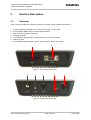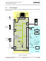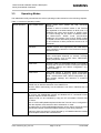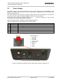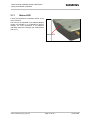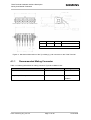
1
TC65 Terminal
Siemens Cellular Engine
Version:
DocID:
01.041
TC65 Terminal_HD_V01.041
Hardware Interface Description
s
s
TC65 Terminal Hardware Interface Description
Strictly Confidential / Released
Document Name:
TC65 Terminal Hardware Interface
Description
Version:
01.041
Date:
September 28, 2005
DocId:
TC65 Terminal_HD_V01.041
Status:
Strictly Confidential / Released
General Notes
Product is deemed accepted by Recipient and is provided without interface to Recipient’s products.
The documentation and/or Product are provided for testing, evaluation, integration and information
purposes. The documentation and/or Product are provided on an “as is” basis only and may contain
deficiencies or inadequacies. The Documentation and/or Product are provided without warranty of any
kind, express or implied. To the maximum extent permitted by applicable law, Siemens further
disclaims all warranties, including without limitation any implied warranties of merchantability,
completeness, fitness for a particular purpose and non-infringement of third-party rights. The entire
risk arising out of the use or performance of the Product and documentation remains with Recipient.
This Product is not intended for use in life support appliances, devices or systems where a
malfunction of the product can reasonably be expected to result in personal injury. Applications
incorporating the described product must be designed to be in accordance with the technical
specifications provided in these guidelines. Failure to comply with any of the required procedures can
result in malfunctions or serious discrepancies in results. Furthermore, all safety instructions regarding
the use of mobile technical systems, including GSM products, which also apply to cellular phones
must be followed. Siemens or its suppliers shall, regardless of any legal theory upon which the claim
is based, not be liable for any consequential, incidental, direct, indirect, punitive or other damages
whatsoever (including, without limitation, damages for loss of business profits, business interruption,
loss of business information or data, or other pecuniary loss) arising out the use of or inability to use
the Documentation and/or Product, even if Siemens has been advised of the possibility of such
damages. The foregoing limitations of liability shall not apply in case of mandatory liability, e.g. under
the German Product Liability Act, in case of intent, gross negligence, injury of life, body or health, or
breach of a condition which goes to the root of the contract. However, Claims for Damages arising
from a breach of a condition which goes to the root of the contract shall be limited to the foreseeable
damage which is intrinsic to the contract, unless caused by intent or gross negligence or based on
liability for injury of life, body or health. The above provision does not imply a change on the burden of
proof to the detriment of the Recipient. Subject to change without notice at any time. The interpretation
of this general note shall be governed and construed according to German law without reference to
any other substantive law.
Copyright
Copying of this document and giving it to others and the use or communication of the contents thereof,
are forbidden without express authority. Offenders are liable to the payment of damages. All rights
reserved in the event of grant of a patent or the registration of a utility model or design.
Copyright © Siemens AG 2005
TC65 Terminal_HD_V01.041
Page 2 of 58
29.09.2005
s
TC65 Terminal Hardware Interface Description
Strictly Confidential / Released
Contents
0
Document History .........................................................................................................6
1
Introduction ...................................................................................................................7
1.1 Related Documents ...............................................................................................7
1.2 Terms and Abbreviations.......................................................................................8
1.3 Type Approval......................................................................................................11
1.4 Safety Precautions...............................................................................................13
2
Key Features of the TC65 Terminal ...........................................................................15
2.1 Technical Requirements for Using TC65 Terminal ..............................................18
3
Interface Description ..................................................................................................19
3.1 Overview..............................................................................................................19
3.2 Block Diagram .....................................................................................................20
3.3 Operating Modes .................................................................................................21
3.4 Terminal Circuit....................................................................................................22
3.5 Power Supply.......................................................................................................23
3.5.1
Switch on TC65 Terminal.......................................................................24
3.5.2
Reset TC65 Terminal.............................................................................24
3.5.3
Switch off TC65 Terminal.......................................................................24
3.5.4
Disconnecting Power Supply .................................................................24
3.6 RS-232 Interface..................................................................................................25
3.7 Audio Interface.....................................................................................................27
3.7.1
Supported Audio Modes ........................................................................28
3.7.2
Speech Processing ................................................................................28
3.8 Antenna Interface ................................................................................................29
3.9 SIM Interface .......................................................................................................29
3.10 IO Interface ..........................................................................................................30
3.10.1 GPIOs ....................................................................................................32
3.10.2 Using GPIO Pin10 as Pulse Counter .....................................................33
3.10.3 I²C Interface ...........................................................................................33
3.10.4 SPI Interface ..........................................................................................34
3.10.5 Analog-to Digital Converter (ADC).........................................................35
3.10.6 RTC Backup Supply...............................................................................36
3.10.7 Power Supply.........................................................................................36
3.10.8 VDD Supply ...........................................................................................36
3.10.9 ON/OFF Switch......................................................................................36
3.11 Status LED...........................................................................................................37
4
Mechanical Characteristics........................................................................................38
4.1 IO Interface Connector ........................................................................................40
4.1.1
Recommended Mating Connector .........................................................41
5
Electrical and Environmental Characteristics..........................................................42
5.1 Characteristics of the Power Supply....................................................................44
5.2 Characteristics of On/Off control..........................................................................45
5.3 Characteristics of the RS-232 interface ...............................................................46
5.4 Characteristics of the SIM Interface for Use with 3V Cards.................................46
5.5 Characteristics of the SIM interface for Use with 1.8V Cards ..............................47
5.6 Characteristics of the Audio Interface..................................................................48
5.6.1
Audio Parameters Adjustable by AT Commands...................................49
5.7 Characteristics of the GPIOs ...............................................................................50
5.8 Characteristics of the Pulse Counter ...................................................................50
TC65 Terminal_HD_V01.041
Page 3 of 58
29.09.2005
s
TC65 Terminal Hardware Interface Description
Strictly Confidential / Released
5.9
5.10
5.11
5.12
5.13
Characteristics of the I2C interface ......................................................................51
Characteristics of the SPI interface .....................................................................51
Characteristics of the ADC Interface ...................................................................52
Characteristics of the RTC Supply.......................................................................52
RF Connector ......................................................................................................53
6
Full Type Approval......................................................................................................54
6.1 Siemens Reference Setup...................................................................................54
6.2 Compliance with FCC Rules and Regulations .....................................................55
6.3 Cable Requirements ............................................................................................55
6.4 Restrictions ..........................................................................................................56
6.5 CE Conformity .....................................................................................................56
6.6 Electromagnetic Compatibility (EMC) ..................................................................56
7
List of Parts and Recommended Accessories .........................................................57
Figures
Figure 1: TC65 Terminal front view ........................................................................................................19
Figure 2: TC65 Terminal rear view.........................................................................................................19
Figure 3: Block diagram .........................................................................................................................20
Figure 4: TC65 Terminal circuit block diagram ......................................................................................22
Figure 5: Female 6-pole Western plug for power supply, ignition, emergency off.................................23
Figure 6: Pin assignment RS-232 (D-Sub 9-pole female)......................................................................25
Figure 7: Audio Western plug (4-pole female) .......................................................................................27
Figure 8: Audio block diagram................................................................................................................27
Figure 9: Pin location of the Molex SIM card holder and position..........................................................29
Figure 10: IO interface connector front view ..........................................................................................30
Figure 11: Location of GPIO pins ...........................................................................................................32
Figure 12: ADC balanced amplifier ........................................................................................................35
Figure 13: Mechanical dimensions.........................................................................................................39
Figure 14: Tyco Micro Mate-N-LOK series on the TC65 Terminal ........................................................40
Figure 15: Mating connector Tyco Micro Mate-N-LOK series................................................................40
Figure 16: Receptacle contact for Tyco Micro Mate-N-LOK series .......................................................40
Figure 17: Mechanical dimensions of the Tyco Mate_N_LOK connector on the TC65 Terminal..........41
Figure 18: Reference equipment for approval........................................................................................54
Tables
Table 1: Overview of operating modes ..................................................................................................21
Table 2: Pin assignment of the Western plug for power supply.............................................................23
Table 3: 9-pole D-Sub (female) RS-232.................................................................................................25
Table 4: Audio modes.............................................................................................................................28
Table 5: Pin assignment – SIM card holder ...........................................................................................29
Table 6: Assignment of the IO interface connector ................................................................................31
Table 7: I²C interface – signal description..............................................................................................33
Table 8: SPI interface – signal description.............................................................................................34
Table 9 : SPI Timing diagram.................................................................................................................34
Table 10: ADC signal description ...........................................................................................................35
Table 11: RTC signal description ...........................................................................................................36
TC65 Terminal_HD_V01.041
Page 4 of 58
29.09.2005
s
TC65 Terminal Hardware Interface Description
Strictly Confidential / Released
Table 12: Mechanical characteristics .....................................................................................................38
Table 13: Electrical and mechanical characteristics of the Micro Mate-N-LOK connector ....................40
Table 14: Ordering information for mating connector Tyco Micro Mate-N-LOK ....................................41
Table 15: Absolute maximum ratings .....................................................................................................42
Table 16: Operating conditions ..............................................................................................................43
Table 17: Highest temperatures .............................................................................................................43
Table 18: Longest duration until 81°C are reached ...............................................................................43
Table 19: Longest duration when GPRS Class Change does not work properly ..................................43
Table 20: Characteristics of the power supply .......................................................................................44
Table 21: Characteristics On/Off control ................................................................................................45
Table 22: Characteristics of the RS-232 interface .................................................................................46
Table 23: Characteristics of the SIM interface for use with 3V cards ....................................................46
Table 24: Characteristics of the SIM interface for use with 1.8V cards .................................................47
Table 25: Characteristics of the audio interface.....................................................................................48
Table 26: Audio Parameters Adjustable by AT Commands...................................................................49
Table 27: Characteristics of the GPIOs..................................................................................................50
Table 28: Characteristics of the pulse counter.......................................................................................50
Table 29: Characteristics of the I2C interface ........................................................................................51
Table 30: Characteristics of the SPI interface........................................................................................51
Table 31: Characteristics of the ADC interface ......................................................................................52
Table 32: Characteristics of the RTC supply..........................................................................................52
Table 33: RF connector..........................................................................................................................53
Table 34: List of parts and accessories..................................................................................................57
TC65 Terminal_HD_V01.041
Page 5 of 58
29.09.2005
s
TC65 Terminal Hardware Interface Description
Strictly Confidential / Released
0
Document History
Preceding document: "TC65 Terminal Hardware Interface Description" Version 01.030
New document: "TC65 Terminal Hardware Interface Description" Version 01.041
Chapter
What is new
Throughout
manual
Changed release number; no further changes
TC65 Terminal_HD_V01.041
Page 6 of 58
29.09.2005
s
TC65 Terminal Hardware Interface Description
Strictly Confidential / Released
1
Introduction
This document describes the hardware of the Siemens TC65 Terminal.
The scope of this document includes interface specifications, electrical issues and mechanical
characteristics of TC65 Terminal. It specifies standards pertaining to wireless applications and
outlines requirements that must be adhered to for successful product design. The TC65 Terminal is a
compact GSM modem for the transfer of data, voice, SMS and faxes in GSM networks. Industrial
standard interfaces and an integrated SIM card reader allow using TC65 Terminal easily as a quad
band GSM terminal.
1.1
[1]
[2]
[3]
[4]
[5]
[6]
[7]
[8]
[9]
Related Documents
TC65 AT Command Set 01.041
TC65 Terminal Release Notes 01.041
Application Note 16: Upgrading TC65 Firmware
Multiplexer User's Guide
Multiplex Driver Developer’s Guide for Windows 2000 and Windows XP
Multiplexer Driver Installation Guide for Windows 2000 and Windows XP
TC65 JAVA User’s Guide
Java doc \wtk\doc\html\index.html
Application Note 24: Application Developer’s Guide
Prior to using the GSM engine read the latest product information provided in the Release Notes.
You can use the following link to visit the Siemens Website:
http://www.siemens.com/wm
TC65 Terminal_HD_V01.041
Page 7 of 58
29.09.2005
s
TC65 Terminal Hardware Interface Description
Strictly Confidential / Released
1.2
Terms and Abbreviations
Abbreviation
Description
ADC
Analog-to-Digital Converter
ANSI
American National Standards Institute
ARP
Antenna Reference Point
B
Thermistor Constant
BER
Bit Error Rate
BTS
Base Transceiver Station
CE
Conformité Européene (European Conformity)
CHAP
Challenge Handshake Authentication Protocol
CS
Coding Scheme
CSD
Circuit Switched Data
CTS
Clear to Send
DAC
Digital-to-Analog Converter
dBm0
Digital level, 3.14dBm0 corresponds to full scale, see ITU G.711, A-law
DCE
Data Communication Equipment (typically modems, e.g. Siemens GSM engine)
DCS 1800
Digital Cellular System, also referred to as PCN
DSP
Digital Signal Processor
DSR
Data Set Ready
DTE
Data Terminal Equipment (typically computer, terminal, printer or, for example, GSM
application)
DTR
Data Terminal Ready
DTX
Discontinuous Transmission
EFR
Enhanced Full Rate
EGSM
Enhanced GSM
EMC
Electromagnetic Compatibility
ESD
Electrostatic Discharge
ETS
European Telecommunication Standard
FCC
Federal Communications Commission (U.S.)
FR
Full Rate
GMSK
Gaussian Minimum Shift Keying
GPIO
General Purpose Input/Output
GPRS
General Packet Radio Service
GSM
Global Standard for Mobile Communications
TC65 Terminal_HD_V01.041
Page 8 of 58
29.09.2005
s
TC65 Terminal Hardware Interface Description
Strictly Confidential / Released
Abbreviation
Description
HiZ
High Impedance
HR
Half Rate
I/O
Input/Output
IMEI
International Mobile Equipment Identity
ISO
International Standards Organization
ITU
International Telecommunications Union
kbps
kbits per second
LED
Light Emitting Diode
Mbps
Mbits per second
MMI
Man Machine Interface
MO
Mobile Originated
MS
Mobile Station (GSM module), also referred to as TE
MT
Mobile Terminated
NTC
Negative Temperature Coefficient
PAP
Password Authentication Protocol
PBCCH
Packet Switched Broadcast Control Channel
PCB
Printed Circuit Board
PCM
Pulse Code Modulation
PCN
Personal Communications Network, also referred to as DCS 1800
PCS
Personal Communication System, also referred to as GSM 1900
PDU
Protocol Data Unit
PPP
Point-to-point protocol
PSU
Power Supply Unit
R&TTE
Radio and Telecommunication Terminal Equipment
RAM
Random Access Memory
RF
Radio Frequency
RTC
Real Time Clock
RTS
Request to Send
Rx
Receive Direction
SELV
Safety Extra Low Voltage
SIM
Subscriber Identification Module
SMS
Short Message Service
SPI
Serial Peripheral Interface
TC65 Terminal_HD_V01.041
Page 9 of 58
29.09.2005
s
TC65 Terminal Hardware Interface Description
Strictly Confidential / Released
Abbreviation
Description
SRAM
Static Random Access Memory
TE
Terminal Equipment, also referred to as DTE
Tx
Transmit Direction
UART
Universal asynchronous receiver-transmitter
URC
Unsolicited Result Code
USSD
Unstructured Supplementary Service Data
TC65 Terminal_HD_V01.041
Page 10 of 58
29.09.2005
s
TC65 Terminal Hardware Interface Description
Strictly Confidential / Released
1.3
Type Approval
TC65 Terminal is designed to comply with the directives and standards listed below.
European directives
99/05/EC
89/336/EC
73/23/EC
2002/95/EC
2002/96/EC
2003/108/EC
“Directive of the European Parliament and of the council of 9 March 1999
on radio equipment and telecommunications terminal equipment and the
mutual recognition of their conformity”, in short referred to as R&TTE
Directive 1999/5/EC
Directive on electromagnetic compatibility
Directive on electrical equipment designed for use within certain voltage
limits (Low Voltage Directive)
Directive of the European Parliament and of the Council
of 27 January 2003 on the restriction of the use of certain
hazardous substances in electrical and electronic
equipment (RoHS)
Directive of the European Parliament and of the Council
on waste electrical and electronic equipment (WEEE)
Directive of the European Parliament and of the Council of 8 December
2003 amending directive 2002/96/ec on waste electrical and electronic
equipment (WEEE)
Standards of North American Type Approval
CFR Title 47
“Code of Federal Regulations, Part 22 and Part 24 (Telecommunications,
PCS)”; US Equipment Authorization FCC
NAPRD.03
“Overview of PCS Type certification review board
Mobile Equipment Type Certification and IMEI control”
PCS Type Certification Review board (PTCRB), Version 3.1.2
RSS133 (Issue2)
Canadian Standard
Standards of European Type Approval
3GPP TS 51.010-1
“Digital cellular telecommunications system (Phase 2); Mobile Station (MS)
conformance specification” V5.10.0
ETSI EN 301 511
“V9.0.2 (2003-03) Candidate Harmonized European Standard
(Telecommunications series) Global System for Mobile communications
(GSM); Harmonized standard for mobile stations in the GSM 900 and DCS
1800 bands covering essential requirements under article 3.2 of the
R&TTE directive (1999/5/EC) (GSM 13.11 version 7.0.1 Release 1998)”
GCF-CC
“Global Certification Forum - Certification Criteria” V3.16.0
ETSI EN 301 489-1
“V1.4.1 Candidate Harmonized European Standard (Telecommunications
series) Electro Magnetic Compatibility and Radio spectrum Matters (ERM);
Electro Magnetic Compatibility (EMC) standard for radio equipment and
services; Part 1: Common Technical Requirements”
TC65 Terminal_HD_V01.041
Page 11 of 58
29.09.2005
s
TC65 Terminal Hardware Interface Description
Strictly Confidential / Released
ETSI EN 301 489-7
“V1.2.1 (2002-08) Candidate Harmonized European Standard
(Telecommunications series) Electro Magnetic Compatibility and Radio
spectrum Matters (ERM); Electro Magnetic Compatibility (EMC) standard
for radio equipment and services; Part 7: Specific conditions for mobile and
portable radio and ancillary equipment of digital cellular radio
telecommunications systems (GSM and DCS)”
EN 60 950-1
Safety of information technology equipment (2001)
Requirements of quality
IEC 60068
Environmental testing
DIN EN 60529
IP codes
TC65 Terminal_HD_V01.041
Page 12 of 58
29.09.2005
s
TC65 Terminal Hardware Interface Description
Strictly Confidential / Released
1.4
Safety Precautions
The following safety precautions must be observed during all phases of the operation, usage, service
or repair of any cellular terminal or mobile incorporating TC65 Terminal. Manufacturers of the cellular
terminal are advised to convey the following safety information to users and operating personnel and
incorporate these guidelines into all manuals supplied with the product. Failure to comply with these
precautions violates safety standards of design, manufacture and intended use of the product.
Siemens AG assumes no liability for customer’s failure to comply with these precautions.
SOS
When in hospitals or other health care facilities, observe the restrictions on the use of
mobiles. Switch off the cellular terminal or mobile if to be instructed to do so by the
guidelines posted in sensitive areas. Medical equipment may be sensitive to RF
energy.
The operation of cardiac pacemakers, other implanted medical equipment and
hearing aids can be affected by interference from cellular terminals or mobiles placed
close to the device. If in doubt about potential danger, contact the physician or the
manufacturer of the device to verify that the equipment is properly shielded.
Pacemaker patients are advised to keep their hand-held mobile away from the
pacemaker, while it is on. This personal subgroup always should check the distance
to the mobile.
Switch off the cellular terminal or mobile before boarding an aircraft. Make sure it
cannot be switched on inadvertently. The operation of wireless appliances in an
aircraft is forbidden to prevent interference with communications systems. Failure to
observe these instructions may lead to the suspension or denial of cellular services to
the offender, legal action, or both.
Check the local and actual laws about these themes.
Do not operate the cellular terminal or mobile in the presence of flammable gases or
fumes. Switch off the cellular terminal when you are near petrol stations, fuel depots,
chemical plants or where blasting operations are in progress. Operation of any
electrical equipment in potentially explosive atmospheres can constitute a safety
hazard.
Your cellular terminal or mobile receives and transmits radio frequency energy while
switched on. Remember that interference can occur if it is used close to TV sets,
radios, computers or inadequately shielded equipment. Follow any special
regulations and always switch off the cellular terminal or mobile wherever forbidden,
or when you suspect that it may cause interference or danger.
Road safety comes first! Do not use a hand-held cellular terminal or mobile while
driving a vehicle unless it is securely mounted in a holder for speakerphone
operation. Before making a call with a hand-held terminal or mobile park the vehicle.
Speakerphones must be installed by qualified personnel. Faulty installation or
operation can constitute a safety hazard.
Check the actual and local laws about these themes.
IMPORTANT!
Cellular terminals or mobiles operate using radio signals and cellular networks. In
that case connections cannot be guaranteed at all times under all conditions.
Therefore, you should never rely solely upon any wireless device for essential
communications, for example emergency calls.
Remember, in order to make calls or receive calls the cellular terminal or mobile must
be switched on in a service area with adequate cellular signal strength.
Some networks do not allow for emergency calls if certain network services or phone
features are in use (e.g. lock functions, fixed dialing etc.). You may need to
deactivate those features before you can make an emergency call.
Some networks require a valid SIM card to be properly inserted in the cellular
terminal or mobile.
TC65 Terminal_HD_V01.041
Page 13 of 58
29.09.2005
s
TC65 Terminal Hardware Interface Description
Strictly Confidential / Released
If a power supply unit is used to supply the device it must meet the demands placed
on SELV circuits in accordance with EN60950. The maximum permissible connection
length between the device and the supply source should not exceed 3m.
According to the guidelines for human exposure to radio frequency energy, an
antenna connected to the SMA jack of the device should be placed at least 20cm
away from human bodies.
TC65 Terminal_HD_V01.041
Page 14 of 58
29.09.2005
s
TC65 Terminal Hardware Interface Description
Strictly Confidential / Released
2
Key Features of the TC65 Terminal
Feature
Implementation
General
Incorporates TC65 module The TC65 module handles all processing for audio, signal and data
within the TC65 Terminal. Internal software runs the application interface
and the whole GSM protocol stack.
Frequency bands
Quad band: GSM 850/900/1800/1900MHz
GSM class
Small MS
Output power
(according to
Release 99, V5)
Class 4 (+33dBm ±2dB) for EGSM850
Class 4 (+33dBm ±2dB) for EGSM900
Class 1 (+30dBm ±2dB) for GSM1800
Class 1 (+30dBm ±2dB) for GSM1900
The values stated above are maximum limits. According to Release 99,
Version 5, the maximum output power in a multislot configuration may
be lower. The nominal reduction of maximum output power varies with
the number of uplink timeslots used and amounts to 3.0dB for 2Tx,
4.8dB for 3Tx and 6.0dB for 4Tx.
Power supply
Single supply voltage 8V to 30V
Operating temperature
-30°C to +65°C ambient temperature
Physical
Dimensions: 130mm x 90mm x 38mm
Weight: approx. 190g
RoHS, WEEE
All hardware components are fully compliant with the EU RoHS and
WEEE Directives
GSM / GPRS features
Data transfer
GPRS
•
Multislot Class 12
•
Full PBCCH support
•
Mobile Station Class B
•
Coding Scheme 1 – 4
CSD
•
V.110, RLP, non-transparent
•
2.4, 4.8, 9.6, 14.4kbps
•
USSD
PPP-stack for GPRS data transfer
TC65 Terminal_HD_V01.041
Page 15 of 58
29.09.2005
s
TC65 Terminal Hardware Interface Description
Strictly Confidential / Released
Feature
Implementation
SMS
•
Point-to-point MT and MO
•
Cell broadcast
•
Text and PDU mode
•
Storage: SIM card plus 25 SMS locations in mobile equipment
•
Transmission of SMS alternatively over CSD or GPRS. Preferred
mode can be user defined.
Fax
Group 3; Class 1
Audio
Speech codecs:
•
Half rate HR (ETS 06.20)
•
Full rate FR (ETS 06.10)
•
Enhanced full rate EFR (ETS 06.50/06.60/06.80)
•
Adaptive Multi Rate AMR
Speakerphone operation, echo cancellation, noise suppression, DTMF,
7 ringing tones
Software
AT commands
AT-Hayes GSM 07.05 and 07.07, Siemens
AT commands for RIL compatibility (NDIS/RIL)
MicrosoftTM compatibility
RIL / NDIS for Pocket PC and Smartphone
Java platform
JDK Version: 1.4.2_07
Java Virtual Machine with interfaces to AT Parser, Serial Interface,
FlashFileSystem and TCP/IP Stack.
Major benefits: seamless integration into Java applications, ease of
programming, no need for application microcontroller, extremely costefficient hardware and software design – ideal platform for industrial
GSM applications.
SIM Application Toolkit
SAT Release 99
TCP/IP stack
Access by AT commands
IP address
IP version 6
Remote SIM Access
TC65 Terminal supports Remote SIM Access. RSA enables TC65
Terminal to use a remote SIM card via its serial interface in addition to
the SIM card locally attached to the dedicated lines of the application
interface. For example, in a vehicle mounted scenario this allows the
driver to access a mobile phone brought into the car from a carembedded phone. The connection between both phones can be a
Bluetooth wireless link or a serial link, e.g. via the car cradle.
The necessary protocols and procedures are implemented according to
the “SIM Access Profile Interoperability Specification of the Bluetooth
Special Interest Group”.
Firmware update
Upgradeable via serial interface.
TC65 Terminal_HD_V01.041
Page 16 of 58
29.09.2005
s
TC65 Terminal Hardware Interface Description
Strictly Confidential / Released
Feature
Implementation
Interfaces
Serial interface
•
8-wire modem interface with status and control lines, unbalanced,
asynchronous
•
Fixed bit rates: 300 bps to 460,800 bps
•
Autobauding: 1,200 bps to 460,800 bps
•
Supports RTS0/CTS0 hardware handshake and software
XON/XOFF flow control.
•
Multiplex ability according to GSM 07.10 Multiplexer Protocol.
I2C
I2C bus for transmission rates up to 400kbps.
Programmable with AT^SSPI command.
Alternatively all pins of the I²C interface are configurable as SPI.
SPI
Serial Peripheral Interface for transmission rates up to 6.5 Mbps.
Programmable with AT^SSPI command.
The I²C interface is not available by using the SPI interface.
Audio
Analog (Microphone, Earpiece)
SIM interface
Supported SIM cards: 3V, 1.8V
Antenna
Connected via antenna SMA connector
Power on/off, Reset
Power-on
Switch on via On/Off push button, ONOFF line on IO interface
connector,
DTR line at RS232 interface or IGT_IN line at power connector
(available with recommended power supply)
Power-off
•
Normal switch-off by AT^SMSO or On/Off push button
•
Emergency switch-off via EMERGOFF line at power connector
•
Automatic switch-off in case of critical temperature and voltage
conditions
Reset
Orderly shutdown and reset by AT command
Special features
Real time clock
Timer functions via AT commands
GPIO
10 I/O pins of the application interface are programmable as GPIO.
Programming is done via AT commands. Alternatively, GPIO pin 10 is
configurable as pulse counter.
Pulse counter
Pulse counter for measuring pulse rates from 0 to 1000 pulses/sec.
If the pulse counter is active the GPIO pin 10 is not available.
ADC inputs
Analog-to-Digital Converter with two balanced analog inputs for
measuring external voltages.
Phonebook
SIM and phone
TC65 Terminal_HD_V01.041
Page 17 of 58
29.09.2005
s
TC65 Terminal Hardware Interface Description
Strictly Confidential / Released
2.1
Technical Requirements for Using TC65 Terminal
•
Computer running Windows 2000, Windows XP
•
1.8V or 3.0V SIM card
•
8 to 30 Volts power supply unit
•
RS-232 cable (for high data rates ≤ 1.5m)
•
UART capable of data rates up to 460800 bps. Usually this requires an appropriate serial adapter
to be installed on the computer.
•
RF antenna
•
Audio handset
•
Customized mating connector for the IO interface connector type Micro Mate-N-LOK.
•
Terminal program to control the COM port, for example Windows HyperTerminal.
•
Access to a GSM/GPRS network providing support of the authentication protocol PAP, CHAP or
MS-CHAP. The GPRS settings of your service provider should be at hand. Please contact your
service provider or follow the link below to obtain all required information.
http://www.gsmworld.com/technology/gprs/operators.shtml
TC65 Terminal_HD_V01.041
Page 18 of 58
29.09.2005
s
TC65 Terminal Hardware Interface Description
Strictly Confidential / Released
3
Interface Description
3.1
Overview
TC65 Terminal provides the following connectors for power supply, interface and antenna:
1.
2.
3.
4.
5.
6.
7.
24-pole GPIO Micro Mate-N-LOK connector for GPIOs, I²C, SPI, ADC
9-pole (female) SUB-D plug for RS-232 serial interface
SMA connector (female) for antenna
On/Off push button
4-pole Western plug (female) for audio accessory, such as a handset
SIM card holder
6-pole Western plug (female) for power supply, ignition, power down signal
1
2
Figure 1: TC65 Terminal front view
3
4
5
6
7
Figure 2: TC65 Terminal rear view
TC65 Terminal_HD_V01.041
Page 19 of 58
29.09.2005
s
TC65 Terminal Hardware Interface Description
Strictly Confidential / Released
3.2
Block Diagram
Figure 3 shows a block diagram of a sample configuration that incorporates a TC65 Terminal and
typical accessories.
GSM
Module
TC65
Antenna
SMA
(female)
RF Cable
SMA-Hirose
Contact
spring
Heat Sink
80 pin B2B
RF
Contact
spring
RS232
RS232
On/Off
Key
Votronic
Handset
or other
audio equipment
VDD (2.9V)
VDD
Audio
I2C device
or
VDD
SPI device
IO connector
ON/OFF
SIM
10xGPIO
100V...240V
AC Adapter
or
DC Supply
2x Analog
measurements
(balanced)
Step Down
DC/DC
Converter
1)
sensors,
relay unit,
switches,
etc.
3.0V Backup Battery
8V...30V
Ignition
8V...30V
Power
In or Out
Emergency-off
1)
Power Supply
Unit
TC65T Mainboard
TC65 Terminal
Application
1) Fast acting fuse 1,25A , (0.9...1.3 A2s) is recommended for 24V vehicle supply only.
Figure 3: Block diagram
TC65 Terminal_HD_V01.041
Page 20 of 58
29.09.2005
s
TC65 Terminal Hardware Interface Description
Strictly Confidential / Released
3.3
Operating Modes
The table below briefly summarizes the various operating modes referred to in the following chapters.
Table 1: Overview of operating modes
Normal operation
GSM / GPRS SLEEP
Various power save modes set with AT+CFUN
command.
Software is active to minimum extent. If the Terminal
was registered to the GSM network in IDLE mode, it is
registered and paging with the BTS in SLEEP mode,
too. Power saving can be chosen at different levels:
The NON-CYCLIC SLEEP mode (AT+CFUN=0)
disables the AT interface. The CYCLIC SLEEP modes
AT+CFUN=7 and 9 alternatively activate and deactivate
the AT interfaces to allow permanent access to all AT
commands.
GSM IDLE
Software is active. Once registered to the GSM network
paging with BTS is carried out. The Terminal is ready to
send and receive.
GSM TALK
Connection between two subscribers is in progress.
Power consumption depends on network coverage
individual settings, such as DTX off/on, FR/EFR/HR,
hopping sequences, antenna.
GPRS IDLE
Terminal is ready for GPRS data transfer, but no data is
currently sent or received. Power consumption depends
on network settings and GPRS configuration (e.g.
multislot settings).
GPRS DATA
GPRS data transfer in progress. Power consumption
depends on network settings (e.g. power control level),
uplink / downlink data rates, GPRS configuration (e.g.
used multislot settings) and reduction of maximum
output power.
POWER DOWN
Normal shutdown after sending the AT^SMSO command, after pressing the
ON/OFF key or after the activation of the ONOFF line.
The RTC works continuously, but the software is not active. Interfaces are not
accessible.
Airplane mode
Airplane mode shuts down the radio part of the module, causes the Terminal to
log off from the GSM/GPRS network and disables all AT commands whose
execution requires a radio connection.
Airplane mode can be controlled by using the AT commands AT^SCFG and
AT+CALA:
With AT^SCFG=MEopMode/Airplane/OnStart the Terminal can be configured to
enter the Airplane mode each time when switched on or reset.
The parameter AT^SCFG=MEopMode/Airplane can be used to switch back and
forth between Normal mode and Airplane mode any time during operation.
Setting an alarm time with AT+CALA followed by AT^SMSO wakes the module
up into Airplane mode at the scheduled time.
TC65 Terminal_HD_V01.041
Page 21 of 58
29.09.2005
s
TC65 Terminal Hardware Interface Description
Strictly Confidential / Released
3.4
Terminal Circuit
lin. Reg.
3.3V
bypass
reverse battery-,
overvoltage-detection
6 pole
Western Jack
80 pole
B2B
BATT+
GND
5
DC/DC
EN
8
2
EMC
4.0V
PWR_IND
fuse
1
EMC
VEXT
+
delay
off
d/dt
EMC
d/dt
EMC
2
1
DTR
Power
GND
EMERG_OFF
IGT_IN
24pin
IO-connector
(male)
on
1
IGT
2
1
EMC
Power
GND
ONOFF
On/OFF-Key
GPIO1-10
SPIDI/
SPICS
I2Cxx
10
10
EMC
2
10xGPIO
EMC
2
4
EMC
SPI / I2C
ADC_IN1,2
2x
4
EMC
GND
2x Analog in
1
VNEG
VDD
EMC
VDDLP
VDD
1
BACKUP
100u
VPOS
VMIC
MIC1
AGND
EP1
CCxx
2
EMC
Feeding Bridge
2
2
5
8
VDD
RS232
level
converter
4 pole
Western Jack
Handset
SIM-Holder
EMC
5
8
EMC
SIM
9 pole
D-Sub (female)
RS232
VPOS
PWR_IND
ASC0
2
DTR
GSM Module TC65
VDD
2
EN
VNEG
SD
BATT+
PWR_IND
EN
lin. Reg2.9V
VDD
VDD
LED
blue
SYNC
SMA
(female)
RF
RF-Cable
Figure 4: TC65 Terminal circuit block diagram
TC65 Terminal_HD_V01.041
Page 22 of 58
29.09.2005
s
TC65 Terminal Hardware Interface Description
Strictly Confidential / Released
3.5
Power Supply
The power supply of the TC65 Terminal has to be a single voltage source of POWER=8V…30V
capable of providing a peak during an active transmission. The uplink burst causes strong ripples
(drop) on the power lines.
The TC65 Terminal is protected from supply voltage reversal and overvoltage. An internal fuse
ensures an electrical safety according to EN60950. This fuse is not removable.
A fast acting fuse 1.25A with melting integral I²t (0.9 … 1.3 A²s) is necessary to use the TC65
Terminal at a 24V power supply system for vehicles.
The power supply must be compliant with the EN60950 guidelines.
Table 2: Pin assignment of the Western plug for power supply
Pin
1
2
3
4
5
6
Signal name
POWER
POWER
EMERGOFF
IGT_IN
GND
GND
Use
Power supply
Power supply
Signal for POWER DOWN mode
Ignition input
Ground
Ground
123 4 5 6
Pin assignment
1 - POWER
2 - POWER
3 - EMERGOFF
4 - IGT_IN
5 - GND
6 - GND
Figure 5: Female 6-pole Western plug for power supply, ignition, emergency off
TC65 Terminal_HD_V01.041
Page 23 of 58
29.09.2005
s
TC65 Terminal Hardware Interface Description
Strictly Confidential / Released
3.5.1
Switch on TC65 Terminal
There are several ways to turn on the TC65 Terminal:
•
Switch on via ON/OFF push button or via ONOFF signal line on IO interface connector: The
major approach is to switch on the TC65 Terminal by pressing the ON/OFF key. The ONOFF pin
of the IO connector is connected in parallel to the ON/OFF key and makes possible to control the
TC65 Terminal from a remote unit.
•
Switch on via IGT_IN line (power supply connector) or DTR line (serial connector). The rising
edge of the IGT_IN line or the DTR line voltage generates an ignition signal (impulse) so that it is
possible to switch on the TC65 Terminal from the host or by remote control.
•
Switch on via recommended power supply unit: By connecting the TC65 Terminal with the
recommended power supply unit the TC65 Terminal starts to work. See Chapter 7 for ordering
information the power supply unit.
Switch on condition: When the TC65 Terminal is off the ON/OFF push button or the ON/OFF signal
line must be asserted for at least 400 ms and then released.
3.5.2
Reset TC65 Terminal
An easy way to reset the TC65 Terminal is entering the command AT+CFUN=x,1. For details on
AT+CFUN please see [1].
3.5.3
Switch off TC65 Terminal
There are several ways to turn off the TC65 Terminal:
•
Software controlled shutdown by AT^SMSO command: The AT^SMSO command lets the TC65
Terminal log off from the network and allows the software to enter into a secure state and safe
data before disconnecting the power supply. The mode is referred to Power-down mode. In this
mode only the RTC stays active.
•
Software controlled shutdown via ON/OFF push button or ONOFF line at IO interface connector:
The TC65 Terminal will be switched off by pressing the ON/OFF push button or by activating the
ONOFF signal for >1s. The shutdown behavior is identical to the behavior when using the
AT^SMSO command.
•
Shutdown via EMEROFF line (power supply connector): The TC65 Terminal will be switched off
by activating the EMERGOFF signal for >1s. All information stored in the volatile memory will get
lost.
•
Automatic shutdown: This takes effect when the board temperature is out of range or when
undervoltage or overvoltage conditions occur.
3.5.4
Disconnecting Power Supply
Before disconnecting the power supply from the POWER pin make sure the TC65 Terminal is in a
safe condition. A save condition is waiting 1s after the "^SHUTDOWN" result code has been indicated.
TC65 Terminal_HD_V01.041
Page 24 of 58
29.09.2005
s
TC65 Terminal Hardware Interface Description
Strictly Confidential / Released
3.6
RS-232 Interface
The serial interface of the TC65 Terminal is intended for the communication between the GSM module
and the host application. This RS-232 interface is a data and control interface for transmitting data, AT
commands and providing multiplexed channels. EMC immunity complies with the vehicular
environment requirements according to EN 301 489-7.
5
4
9
3
8
2
7
1
6
Figure 6: Pin assignment RS-232 (D-Sub 9-pole female)
Table 3: 9-pole D-Sub (female) RS-232
Pin no.
Signal name
I/O
Function of application
1
DCD
O
Data Carrier Detected
2
RXD
O
Receive Data
3
TXD
I
Transmit Data
4
DTR
I
Data Terminal Ready
Attention: Low-to-high transition of the DTR line activates the
ignition signal of the GSM module
5
GND
-
Ground
6
DSR
O
Data Set Ready
7
RTS
I
Request To Send
8
CTS
O
Clear To Send
9
RING
O
Ring Indication
TC65 Terminal_HD_V01.041
Page 25 of 58
29.09.2005
s
TC65 Terminal Hardware Interface Description
Strictly Confidential / Released
GSM Terminal (DCE)
Application (DTE)
TXD0
TXD
RXD0
RXD
RTS0
RTS
CTS0
CTS
DTR0
DTR
DSR0
DSR
DCD0
DCD
RING0
RING
TC65 Terminal is designed for use as a DCE. Based on the conventions for DCE-DTE connections it
communicates with the customer application (DTE) using the following signals:
•
Port TxD @ application sends data to TXD of TC65 Terminal
•
Port RxD @ application receives data from RXD of TC65 Terminal
The RS-232 interface is implemented as a serial asynchronous transmitter and receiver conforming to
ITU-T V.24 Interchange Circuits DCE. It is configured for 8 data bits, no parity and 1 stop bit and can
be operated at fixed bit rates from 300bps to 460,800bps. Autobauding supports bit rates from 1,2bps
to 460,800bps. Hardware handshake using the /RTS and /CTS signals and XON/XOFF software flow
control are supported.
In addition the modem control signals DTR, DSR, DCD and RING are available. The modem control
signal RING (Ring Indication) can be used to indicate, to the cellular device application, that a call or
Unsolicited Result Code (URC) is received.
TC65 Terminal_HD_V01.041
Page 26 of 58
29.09.2005
s
TC65 Terminal Hardware Interface Description
Strictly Confidential / Released
3.7
Audio Interface
The audio interface provides one analog input for a microphone and one analog output for an
earpiece.
•
The microphone input and the earpiece output are balanced.
•
For electret microphones a supply source is implemented.
•
The microphone supply characteristics are optimized for the recommended Votronic handset. For
ordering Information see Chapter 7.
•
This handset has been used for the reference handset for type approval. An extra approval must
be obtained for integrating other handsets or amplifiers.
The amplification of sending direction, receiving direction and sidetone depends on the current audio
mode.
EMC immunity complies with the vehicular environment requirements according to EN 301 489-7.
12 3 4
Pin assignment
1 - MICN (Microphone - )
2 - EPN (Earpiece)
3 - EPP (Earpiece)
4 - MICP (Microphone + )
Figure 7: Audio Western plug (4-pole female)
Microphone
Feeding
A
MIC
Speech
coder
D
<inCalibrate>
- ... 0dB
8
<inBbcGain>
0dB...42dB in steps
of 6dB
8
<sideTone>
- ... 0dB
EP
A
Speech
decoder
D
<outCalibrate[n]>
n = 0, ..., 4
<outBbcGain>
-18dB ... 0dB in steps
of 6dB
AT parameters are given in brackets <...>
and marked red and italic.
Figure 8: Audio block diagram
TC65 Terminal_HD_V01.041
Page 27 of 58
29.09.2005
s
TC65 Terminal Hardware Interface Description
Strictly Confidential / Released
3.7.1
Supported Audio Modes
The audio interface can be configured by AT commands. Refer to [1] for details.
The electrical characteristics of the voiceband part vary with the audio mode. Specifications are listed
in Table 4. To suit several types of audio equipment, three audio modes given by default can be
selected by the AT command AT^SNFS.
Regarding audio performance, compliance with the TS 51010-1 specification and GCF
recommendations has been certified for the parameters provided by audio mode 1 and audio
interface 1. The settings are optimized for the reference handset (type Votronic) connected to the
TC65 Terminal (see chapters 6.1 and 7). To ensure that the reference parameters are always within
the limits demanded by the standards they cannot be changed by AT command. Furthermore, the
reference parameters are set as factory default.
In audio mode 4 and 5, the gain in the microphone, earpiece and the sidetone path can be adjusted
from the cellular device application by using further AT commands.
Please note that the 2nd audio interface of the TC65 module is not connected in the TC65 Terminal.
Audio modes 2, 3 and 6 can be selected by setting AT^SAIC=2,1,1, for further details refer to [1].
Table 4: Audio modes
Mode No
AT^SNFS=
1 (Default settings, 4
not adjustable)
5
Name
Default Handset
User Handset
Plain Codec 1
Purpose
Recommended
handset
User provided
handset
Direct access to
speech coder
Gains programmable via AT
command
NO
YES
YES
Sidetone
YES
YES
YES
Volume control
NO
YES
YES
Echo control (send)
Cancellation and
suppression
Cancellation and
suppression
NO
Noise suppression
YES
YES
NO
MIC input signal for 0dBm0
@ 1024 Hz
(at default gain settings)
12.5 mV
12.5 mV
400 mV
Earpiece output signal in mV eff.
@ 0dBm0, 1024 Hz, no load (at
default gain settings);
@ 3.14 dBm0
475 mV
475 mV (default @
max volume)
1.5 V
Sidetone gain (at default
settings)
24.9 dB
3.7.2
6.0 Vpp
24.9 dB
-∞ dB
Speech Processing
The speech samples from the ADC are handled by the DSP of the baseband controller to calculate
e.g. amplifications, sidetone, echo cancellation or noise suppression depending on the configuration of
the active audio mode. These processed samples are passed to the speech encoder. Received
samples from the speech decoder are passed to the DAC after post processing (frequency response
correction, adding sidetone etc.).
Full rate, half rate, enhanced full rate, adaptive multi rate (AMR), speech and channel encoding
including voice activity detection (VAD) and discontinuous transmission (DTX) and digital GMSK
modulation are also performed on the GSM baseband processor.
Note: With regard to acoustic shock, the cellular application must be designed to avoid sending false
AT commands that might increase the amplification, e.g. for a high sensitive earpiece.
TC65 Terminal_HD_V01.041
Page 28 of 58
29.09.2005
s
TC65 Terminal Hardware Interface Description
Strictly Confidential / Released
3.8
Antenna Interface
In order to send or receive data connect an external RF antenna to the SMA connector which is
internally connected to the RF signal of the GSM module.
Please consider that the recommended antenna equipment has been chosen to achieve optimum RF
performance when operating the TC65 Terminal. Siemens does not accept warranty claims for
damage caused by inappropriate equipment connected to the antenna connector.
3.9
SIM Interface
The SIM interface is intended for 3V and 1.8V SIM cards. The card
holder is a five wire interface according to GSM 11.11. A sixth pin
has been added to detect whether or not the SIM card drawer is
inserted.
Removing and inserting the SIM card during operation requires the
software to be reinitialized. Therefore, after reinserting the SIM card
it is necessary to restart TC65 Terminal.
Note: No guarantee can be given nor any liability accepted, if loss of
data is encountered after removing the SIM card during operation.
Also, no guarantee can be given for properly initializing any SIM
card that the user inserts after having removed a SIM card during
operation. In this case the TC65 Terminal must be restarted by the application.
Figure 9: Pin location of the Molex SIM card holder and position
Table 5: Pin assignment – SIM card holder
Pin number on Signal name
holder
I/O
Function
1
VSIM
O
Supply voltage for SIM card is generated by the module.
2
CCRST
O
Chip card reset, prompted by the module
3
CCCLK
O
Chip card clock
GND
-
Ground
5
CCVPP
-
Not connected
6
CCIO
I/O
7
CCIN
I
4,8
Serial data line, bi-directional
Chip card drawer detection
0 = Chip card drawer inserted
1 = Chip card drawer not inserted
Input on the baseband processor for detecting the chip
card drawer in the holder; if the SIM is removed during
operation the interface is shut down immediately to prevent
destruction of the SIM.
TC65 Terminal_HD_V01.041
Page 29 of 58
29.09.2005
s
TC65 Terminal Hardware Interface Description
Strictly Confidential / Released
3.10
IO Interface
Via the IO interface connector the following interfaces and functions are provided.
•
Programmable GPIOs
•
I²C bus
•
SPI interface
•
Two analog inputs (balanced)
•
Power supply
•
Backup supply
•
VDD supply
•
On/Off switch of the TC65 Terminal
•
Pulse counter
The total cable length of the digital lines for I²C and SPI interfaces should not exceed 150mm.
24
13
12
1
Figure 10: IO interface connector front view
TC65 Terminal_HD_V01.041
Page 30 of 58
29.09.2005
s
TC65 Terminal Hardware Interface Description
Strictly Confidential / Released
Table 6: Assignment of the IO interface connector
Pin
Signal name
I/O
Description
1
I2CCLK_SPICLK
O
I2C or SPI Clock
2
I2CDAT_SPIDO
I/O
I2C Data or SPI Data out
3
GPIO3
I/O
Programmable GPIO
4
GPIO4
I/O
Programmable GPIO
5
GPIO5
I/O
Programmable GPIO
6
GPIO6
I/O
Programmable GPIO
7
GPIO1
I/O
Programmable GPIO
8
GPIO2
I/O
Programmable GPIO
9
ADC2_IN_P
I
Balanced analog 2 positive input
10
ADC2_IN_N
I
Balanced analog 2 negative input
11
BACKUP
I
Backup battery
12
GND
13
SPICS
O
SPI Select
14
SPIDI
I
SPI Data In
15
GPIO9
I/O
Programmable GPIO
16
GPIO10
I/O
Programmable GPIO/ Pulse counter
17
GPIO7
I/O
Programmable GPIO
18
GPIO8
I/O
Programmable GPIO
19
VDD
O
Signal supply voltage
20
ONOFF
I
Ignition
21
ADC1_IN_P
I
Balanced analog 1 positive input
22
ADC1_IN_N
I
Balanced analog 1 negative input
23
GND
24
POWER
TC65 Terminal_HD_V01.041
Ground for power supply
Signal ground
I
Power supply
Page 31 of 58
29.09.2005
s
TC65 Terminal Hardware Interface Description
Strictly Confidential / Released
3.10.1
GPIOs
The TC65 Terminal provides 10 GPIO pins at the IO interface connector. Each GPIO line is ESD
protected and a serial resistor of 100 Ohm is added.
This avoids short circuits and is especially important in the first stages of development where the Java
application is not yet fully implemented.
The signal direction (input/output) of the GPIO lines is selectable with AT commands.
Figure 11 shows the position of the GPIO pins at the IO interface connector.
Alternatively GPIO pin10 can be used to configure, to start or stop a pulse counter for an input range
of 0 to 1000 pulses per second. If the pulse counter is active the pin10 is not available for GPIO
signals.
The GPIOs and the pulse counter can be configured via the following AT commands: AT^SPIO,
AT^SCPIN, AT^SCPOL, AT^SCPORT, AT^SDPORT, AT^SGIO, AT^SSIO, AT^SCCNT, AT^SSCNT.
For details please refer to [1].
GPIO GPIO GPIO GPIO
pin 8 pin 7 pin 10 pin 9
24
13
12
1
GPIO GPIO GPIO GPIO GPIO GPIO
pin 2 pin 1 pin 6 pin 5 pin 4 pin 3
Figure 11: Location of GPIO pins
TC65 Terminal_HD_V01.041
Page 32 of 58
29.09.2005
s
TC65 Terminal Hardware Interface Description
Strictly Confidential / Released
3.10.2
Using GPIO Pin10 as Pulse Counter
The GPIO10 pin can be assigned two different functions selectable by AT command:
•
•
The AT^SCPIN command configures the pin for use as GPIO.
With AT^SCCNT and AT^SSCNT the pin can be configured and operated as pulse counter.
Both functions exclude each other. The pulse counter disables the GPIO functionality, and vice versa,
the GPIO functionality disables the pulse counter.
Detailed AT command descriptions can be found in [1].
The pulse counter is designed to measure signals from 0 to 1000 pulses per second. It can be
operated either in Limit counter mode or Start-Stop mode. Depending on the selected mode the
counted value is either the number of pulses or the time (in milliseconds) taken to generate a number
of pulses specified with AT^SCCNT.
The Limit counter mode, the displayed measurement result (URC “^SSCNT: <count>”) implies an
inaccuracy <5ms. In Start-Stop mode, you can achieve 100% accuracy if you take care that no pulses
are transmitted before starting the pulse counter (AT^SSCNT=0 or 1) and after closing the pulse
counter (AT^SSCNT=3).
3.10.3
I²C Interface
The I²C interface is located at the IO interface connector of the TC65 Terminal.
I²C is a serial, 8-bit oriented data transfer bus for bit rates up to 400kbps in fast mode. It consists of
two lines. These are the serial data line I2CDAT and the serial clock line I2CCLK.
The TC65 Terminal acts as a single master device, e.g. the clock I2CCLK is driven by the Terminal.
The connection I2CDAT is a bi-directional line.
Each device which is connected to the bus is software addressable by a unique address and simple
master/slave relationships exists at all times. The Terminal operates as master-transmitter or as
master-receiver. The customer application transmits or receives data only on request of the Terminal.
To configure and activate the I2C interface use the AT^SSPI command described in [1].
The I2C interface is only available if the pins 1 and 2 of the IO interface connector are not used as SPI
interface.
Table 7: I²C interface – signal description
Signal name
Pin
Description
I2CDAT_SPIDO
1
Data in/out – bidirectional serial data line
I2CCLK_SPICLK
2
Serial clock line
TC65 Terminal_HD_V01.041
Page 33 of 58
29.09.2005
s
TC65 Terminal Hardware Interface Description
Strictly Confidential / Released
3.10.4
SPI Interface
The SPI interface is located on the IO interface connector of the TC65 Terminal.
The SPI (Serial Peripheral Interface) is a synchronous serial interface for controlling and data transfer
between the TC65 Terminal and a connected application. Only one application can be connected to
the Terminal’s SPI.
The SPI consists of four lines. These are the two data lines SPIDI/SPIDO, the clock line SPICLK and
the chip select line SPICS.
The TC65 Terminal acts as a single master device, e.g. the clock SPICLK is driven by the TC65
Terminal. Whenever the SPICS pin is in a low state, the SPI bus is activated and data can be
transferred from the Terminal and vice versa. The SPI interface uses two independent lines for data
input (SPIDI) and data output (SPIDO). The interface supports transmission rates up to 6.5Mbit/s.
Transfer rates >1.083Mbps and a length of the cable >150mm are not recommended.
The SPI interface is only available if the pins 1 and 2 of the IO interface connector are not used as I2C
interface.
Table 8: SPI interface – signal description
Signal name
Pin
Description
SPICS
13
Chip select – selects and activates the external device via a low signal.
SPIDI
14
Data in – serial data input line (from the external device to the TC65
Terminal)
I2CDAT_SPIDO
1
Data out – serial data output line (from the TC65 Terminal to the
external device)
I2CCLK_SPICLK
2
Serial clock line
The SPI Interface can be used in 4 different modes.
Table 9 : SPI Timing diagram
Clock phase
SPI MODE 0
SPI MODE 1
SPICS
SPICLK
SPICLK
SPIDO
SPIDO
SPIDI
SPIDI
Clock polarity
SPICS
Sample
Sample
SPI MODE 2
SPI MODE 3
SPICS
SPICS
SPICLK
SPICLK
SPIDO
SPIDO
SPIDI
SPIDI
Sample
TC65 Terminal_HD_V01.041
Sample
Page 34 of 58
29.09.2005
s
TC65 Terminal Hardware Interface Description
Strictly Confidential / Released
3.10.5
Analog-to Digital Converter (ADC)
The two balanced analog inputs are used for measuring external DC voltages in a range of 0V to
5.0V.
Note: Only positive differential voltage can be handled because of the input requirement of ADC.
Table 10: ADC signal description
Signal name
Pin
Description
ADC1_IN_N
22
Negative voltage
ADC1_IN_P
21
Positive voltage (must be more positive than ADC2_IN_N)
ADC2_IN_N
10
Negative voltage
ADC2_IN_P
9
Positive voltage (must be more positive than ADC2_IN_N)
Gain = appr. 0.48
GPIOConnector
ADCx_IN_P
Cellular
Engine
TC65
21,9
G=2
475k
0V...5.0V
2,3
ADCx_IN
0V...2.4V
2x150k
ADCx_IN_N
22,10
56
6V transil diods
for ESD protection
AGND
475k
Figure 12: ADC balanced amplifier
Use the command AT^SRADC described in [1] to configure the analog inputs and to get the
measurement results.
Note:
It is necessary to recalculate measurement results because an amplifier is used to scale down the
ADCx_IN input voltage of the TC65 Terminal (5V) to the ADCx_IN input voltage of the in-built TC65
module (2.4V).
Two parameters (determined and stored by factory) have to be used for offset compensation and for
consideration of gain and tolerances:
Use the command AT^SAADC described in [1] to read out the required parameters:
<ofsx>: Offset
<ampx> : Amplification factor (Gain*4096)
x=1 for Input 1 or 2 for input 2
To recalculate the exact voltages [mV] measured at the ADCx_IN input use the following equation:
Value[mV] = (<value> from AT^SRADC - <ofsx>) * <ampx> / 4096
TC65 Terminal_HD_V01.041
Page 35 of 58
29.09.2005
s
TC65 Terminal Hardware Interface Description
Strictly Confidential / Released
3.10.6
RTC Backup Supply
The Real Time Clock (RTC) is supplied from a separate voltage inside the TC65T Terminal which is
also active when the GSM module is in POWER-DOWN mode. An alarm function is provided for
activating/deactivating GSM module (activating only to alarm mode).
You can use the BACKUP pin on the 24pole I/O connector to backup the RTC from an external
battery (rechargeable or non-chargeable).
Table 11: RTC signal description
Signal name
Pin
Description
BACKUP
11
External battery
GND
12
Ground
If no backup battery is connected then a 100uF capacitor supplies the RTC about 6s during power
interruptions.
3.10.7
Power Supply
The two pins of the power supply at the IO interface connector are directly connected to two pins of
the Western Jack for power supply. This allows supplying the TC65 Terminal by using the Power
connector or via the IO interface connector.
3.10.8
VDD Supply
The VDD pin at the IO interface connector may be used for supplying external circuit devices or
applications and indicates the following states of the TC65 Terminal:
•
VDD output voltage = 2.9V @ max. 50mA indicates Normal Operation mode or Airplane mode
•
VDD output voltage = 0V indicates Power Down mode
3.10.9
ON/OFF Switch
If the ONOFF pin at the IO interface connector is active low. It can be used to switch on or switch off
the TC65 Terminal.
For more information to switch on or off the Terminal please refer to chapter 3.5.1 and 3.5.3.
TC65 Terminal_HD_V01.041
Page 36 of 58
29.09.2005
s
TC65 Terminal Hardware Interface Description
Strictly Confidential / Released
3.11
Status LED
A blue LED displays the operating status of the
TC65 Terminal.
The LED can be operated in two different display
modes: AT^SSYNC=1 or AT^SSYNC=2 (factory
default). For more information of the different
operating states and changing this mode please
refer to [1].
Status LED
TC65 Terminal_HD_V01.041
Page 37 of 58
29.09.2005
s
TC65 Terminal Hardware Interface Description
Strictly Confidential / Released
4
Mechanical Characteristics
Table 12: Mechanical characteristics
Weight
190g
Dimensions (max) L x W x H
130mm x 90mm x 38mm
Temperature range
-30°C to +65°C ambient temperature
Protection class
IP40 (Avoid exposing TC65 Terminal to liquid or moisture, for
example do not use it in a shower or bath.)
Mechanical vibrations Amplitude 7.5mm at 5-200Hz sinus
Max. pulse acceleration
30g pulse with 18 ms duration time
Air humidity
5...80% (non condensing)
Class of flammability
UL94 HB
Casing material
PC/ABS Cycoloy 1200 HF
TC65 Terminal_HD_V01.041
Page 38 of 58
29.09.2005
s
TC65 Terminal Hardware Interface Description
Strictly Confidential / Released
Figure 13: Mechanical dimensions
TC65 Terminal_HD_V01.041
Page 39 of 58
29.09.2005
s
TC65 Terminal Hardware Interface Description
Strictly Confidential / Released
4.1
IO Interface Connector
This chapter provides specifications for the 24-pin IO interface connector which serves the I2C, SPI
and GPIO interfaces of the Terminal. The type of the receptacle assembled on the TC65 Terminal is
Micro Mate-N-LOK 3mm from Tyco Electronics. Mating headers can be chosen from the Tyco Micro
Mate-N-LOK Series. For latest product information please contact your Micro Electronics dealer or
visit the Tyco home page, for example http://www.tycoelectronics.com.
Figure 14: Tyco Micro Mate-N-LOK series on the
TC65 Terminal
Figure 15: Mating connector Tyco Micro Mate-NLOK series
Figure 16: Receptacle contact for Tyco Micro
Mate-N-LOK series
Table 13: Electrical and mechanical characteristics of the Micro Mate-N-LOK connector
Parameter
Specification
Number of contacts
24
Voltage rating
250V
Current rating
5A max.
Resistance
0.02 Ohm max. per contact
Dielectric withstanding voltage
1500VAC
Operating temperature
-40°C...+105°C
Contact centerline
3.0mm
Mating force
6.67N max. per contact
Contacts packaging method
Contacts available in strip form or loose piece
(24 pieces/housing for full assembly)
Receptacle housing material
Flame-retardant black thermoplastic
Contact material
Phosphor bronze
TC65 Terminal_HD_V01.041
Page 40 of 58
29.09.2005
s
TC65 Terminal Hardware Interface Description
Strictly Confidential / Released
DIM X
DIM Y
DIM Z
Number of Positions
40.00
36.86
33.00
24
Values in mm
Figure 17: Mechanical dimensions of the Tyco Mate_N_LOK connector on the TC65 Terminal.
4.1.1
Recommended Mating Connector
Table 14: Ordering information for mating connector Tyco Micro Mate-N-LOK
Item
Number of positions
Ordering number
Micro Mate-N-LOK 3mm
24
2-794617-4
Crimp Snap-IN Receptacle Contacts
794606-*
794607-*
TC65 Terminal_HD_V01.041
Page 41 of 58
29.09.2005
s
TC65 Terminal Hardware Interface Description
Strictly Confidential / Released
5
Electrical and Environmental Characteristics
Table 15: Absolute maximum ratings
Parameter
Port / Description
Min.
Max.
Unit
Supply voltage
POWER
-33
+33
V
Input voltage for Ignition
IGT_IN
-30
+30
V
Input voltage for emergency
off
EMERGOFF
-25
+30
V
RS-232 input voltage range
TXD0, DTR0, RTS0
-30
+30
V
RXD0, CTS0, DSR0, DCD0, RING0
(No DC Input)
-0.3
+0.3
2)
GPIO1 – GPIO10, I2CCLK_SPICLK,
I2CDAT_SPIDO, SPICS, SPIDI,
I2CDAT_SPIDO
-0.3
+3.05
1)
+0.3
2)
Analog Input
ADC1_IN_P, ADC1_IN_N, ADC2_IN_P,
ADC2_IN_N
-6
+6
Backup battery
BACKUP
-4.7
+4.7
Digital GPIO, SPI, I2C
On/Off- line
VDD supply voltage
ONOFF (No DC Input)
-0.3
VDD (No DC Input)
-0.3
V
V
V
V
+0.3
3)
V
+0.3
2)
V
0.6
2)
3.1
1,4)
Microphone input line AC
voltage (pins to GND)
MICP1, MICN1
(No DC Input)
Earpiece voltage (idle, no
power)
EPP1, EPN1
(No DC Input)
-0.3
+0.3
Antenna Connector
No DC input
0
0
V
Immunity against air
discharge of static electricity
All connectors (lines)
-8
+8
kV
Immunity against contact
discharge of static electricity
All connectors (lines)
-4
+4
kV
Protection Class
IP40 (avoid exposing to liquid or moisture, for
example do not use it in a shower or bath)
IP 40
Mechanical vibrations
amplitude
@ 5-200Hz
7.5
mm
Mechanical pulseacceleration
@ 18ms duration
30
G
1)
2)
3)
4)
2)
Vpp
V
for all operation modes
for Power Down and Power Off
only Power Off
A call is established or AT command “AT^SNFM=,1” was executed
TC65 Terminal_HD_V01.041
Page 42 of 58
29.09.2005
s
TC65 Terminal Hardware Interface Description
Strictly Confidential / Released
Table 16: Operating conditions
Parameter
Min
Typ
Max
Ambient temperature
-30
25
65
Supply voltage VPOWER
measured at (6-pole) western
jack plug (1, 2 to 5,6)
7.6 lowest voltage
(minimum peak) incl. all
ripple and drops
12
30
1)
Unit
°C
V
1)
Continuous operation at 65°C environmental temperature is not possible in every operating mode due to intrinsic heating of
the TC65 Terminal.
The level of intrinsic heating depends on several factors depending on the level of the supply voltage, the operating mode
(GPRS/GSM) and the network coverage. The maximum possible environmental temperature in GPRS Class 12 operating
mode (MS-configuration 1down/4up, PCL5/Gamma3, 12V supply voltage, 900MHz band, with power reduction) is about 45°C.
When this temperature is exceeded the TC65 Terminal will send a request to the base station for changing the GPRS-Class
(e.g. from GPRS Class 12 to GPRS Class 8). At a successful change of the GPRS class the intrinsic heating of the TC65
Terminal will be reduced. If the board temperature decreases by an amount of 15°C the GPRS Class will be stepped up again.
Continuous operation in Talk mode is possible up to an environmental temperature of about 67°C (12V, 900MHz, PCL5). With
decreasing transmit power of the TC65 Terminal, the maximum possible environmental temperature increases at which a
GPRS continuous operation at PCL5/Gamma3 is possible.
For a short time it is also possible to establish a GPRS Class 12 connection at PCL5/Gamma3 and at an ambient temperature
of 65°C. Starting a data download in GPRS Class 12 mode with power reduction at 65°C environmental temperature the
request for a change of the GPRS Class will be enabled after 7 minutes.
This information applies to 12V supply voltage. At 8V resp. 30V the intrinsic heating is higher, whereby the maximum possible
environmental temperature will be lower.
Special values of maximum ratings
The following table shows the highest possible ambient temperatures at which the temperature of the NTC will reach a final
value of 81°C (GPRS Class 10,12 Temperature of GPRS Class Change) or the final shut down temperature 90°C (GPRS
Class 8 and Voice Call).
Table 17: Highest temperatures
Terminal horizontal, normal position
Highest possible ambient temperature
GPRS Class 8 PCL5/Gamma3
67°C
GPRS Class 10 PCL5/Gamma3
48°C
GPRS Class 12 PCL5/Gamma3 with Power Reduction
45°C
GPRS Class 12 PCL5/Gamma3 without Power Reduction
34°C
The following table shows the longest possible duration of a connection until 81°C (Temperature of GPRS Class Change) are
reached at the NTC when the ambient temperature is 65°C.
Table 18: Longest duration until 81°C are reached
Terminal horizontal, normal position
Longest possible duration of connection
GPRS Class 10 PCL5/Gamma3
11 minutes
GPRS Class 12 PCL5/Gamma3 with Power Reduction
7 minutes
GPRS Class 12 PCL5/Gamma3 without Power Reduction
---
The following table shows the longest possible duration of connection when the GPRS Class Change from GPRS Class 12 or
10 to GPRS Class 8 did not work properly and 90°C (Temperature of Hardware shut off) will be reached at the NTC (ambient
temperature is 65°C).
Table 19: Longest duration when GPRS Class Change does not work properly
Terminal horizontal, normal position
Longest possible duration of connection
GPRS Class 8 PCL5/Gamma3
Continuous operation
GPRS Class 10 PCL5/Gamma3
22 minutes
GPRS Class 12 PCL5/Gamma3 with Power Reduction
14 minutes
GPRS Class 12 PCL5/Gamma3 without Power Reduction
---
TC65 Terminal_HD_V01.041
Page 43 of 58
29.09.2005
s
TC65 Terminal Hardware Interface Description
Strictly Confidential / Released
5.1
Characteristics of the Power Supply
Table 20: Characteristics of the power supply
Parameter
Description
Conditions
Min
VPOWER
Operating Voltage
for one minute
8
Power Down mode
SLEEP mode
Average supply current
(average time 3 min.)
IPOWER
@25°C
@ worst case:
GSM 900 max power
level
IDLE mode
TALK mode
Data GPRS 1Tx / 4Rx
Data GPRS 2Tx / 3Rx
(Power reduction = 3dB)
Data GPRS 4Tx / 1Rx
(Power reduction = 6dB)
IPOWER_P
tPLUS-Fail
2)
Max Unit
12
30
V
33
V
@8V
0.45
@12V
0.50
@30V
0.80
@8V
40
@12V
29
@30V
18
@8V
50
@12V
36
@30V
21
@8V
277
@12V
184
@30V
82
@8V
260
@12V
173
@30V
77
@8V
378
@12V
248
@30V
108
@8V
500
@12V
330
@30V
140
@8V
1500
@12V
910
@30V
340
Peak supply current
during transmission slot
(577µs * No. of Tx every
4.6ms)
Power control level for
Pout max
Allowed power fail time
without terminal reset or
power down
After this time the Terminal will be
reset or switched off
Allowed power fail time
without RTC reset
1)
Typ
Backup Battery not connected,
After this time the RTC will be reset
µA
mA
mA
mA
mA
mA
mA
mA
1
6
ms
s
1)
Lowest voltage (minimum peak) incl. all ripple and drops >7.6V including voltage drop, ripple and spikes, measured at
western jack (6-pole) pin (1 to 6)
2)
Typical values measured with antenna impedance = 50Ohm (return loss >20dB)
Maximum values measured with mismatched antenna
TC65 Terminal_HD_V01.041
Page 44 of 58
29.09.2005
s
TC65 Terminal Hardware Interface Description
Strictly Confidential / Released
5.2
Characteristics of On/Off control
Table 21: Characteristics On/Off control
Function
Signal name
IO
Signal form and level
Comment
Emergency
OFF
EMERGOFF
I
RI ≈ 100kOhm
Emergency-off switches the
power supply of the Terminal
off.
VLmax = 0.8V
VLmin = -0.3V
VHmin = 4.5V
VHmax = 30V
signal ___________|~~~~~~~~~~~~|__
| ≥ 1s
| ≥ 1s |
Ignition
IGT_IN
I
Data stored in the volatile
memory will be lost, if used
the emergency off.
Rise time ≤ 100ms
If unused keep pin open.
RI ≈ 100kOhm, CI ≈ 100nF
This signal switches the
mobile ON.
VLmax = 0.8V
VLmin = -0.3V
VHmin = 8V
VHmax = 30V
It´s possible to connect
IGT_IN directly with POWER.
signal ___________|~~~~~~~~~~~~|__
| ≥ 0.5s | ≥ 0.5s |
If unused keep pin open.
rise time ≤ 100ms
ONOFF
I
RI ≈ 30kΩ, CI ≈ 10nF
This signal switches the
mobile ON and OFF.
VILmax = 0.5V at Imax = -150µA
VOHmax = 4.2V
ON
OFF
~~~~
|________|~~~~~~~~~~~~~|________|~~~
| ≥ 0.4s | ≥ 2s
| ≥ 1s
|
RS232
DTR
I
This line must be driven low
by an open drain or open
collector driver.
rise time ≤ 1ms
If unused keep pin open.
VImin = ±3V
This signal switches the
module ON with the low high
transition.
signal
~~~
|________|~~~~~~~~~~~~~~~
| ≥ 0.5s | ≥ 0.5s |
Rise time ≤ 1ms
TC65 Terminal_HD_V01.041
Page 45 of 58
29.09.2005
s
TC65 Terminal Hardware Interface Description
Strictly Confidential / Released
5.3
Characteristics of the RS-232 interface
Table 22: Characteristics of the RS-232 interface
Function
Signal name
IO
Signal from and level
RS232
TXD
I
RImin = 3kOhm
RTS
I
DTR
I
5.4
RXD
O
CTS
O
DSR
O
DCD
O
RING
O
VILmax = 0.6V
VIHmin = 2.4V
VImax = ±25V
VOmin = ±5V at 3kOhm load
Leakage Current max = ±25µA at
Module power down.
Comment
If lines are unused keep
pin open.
It could be possible to start
the module with DTR.
Characteristics of the SIM Interface for Use with 3V Cards
Table 23: Characteristics of the SIM interface for use with 3V cards
Function
Signal name IO Signal form and level
Reset
CCRST
O
Data IO
CCIO
I/O RI ≈ 4.7kΩ
VILmax = 0.75V
VILmin = -0.3V
VIHmin = 2.1V
VIHmax = CCVCCmin + 0.3V = 3.05V
RO ≈ 47Ω
VOLmax = 0.25V at I = +1mA
VOHmin = 2.5V at I = -0.5mA
VOHmax = 2.95V
RO ≈ 100Ω
VOLmax = 0.3V at I = +1mA
VOHmin = 2.5V at I = -0.5mA
VOHmax = 2.95V
Clock
CCCLK
O
RO ≈ 100Ω
VOLmax = 0.3V at I = +1mA
VOHmin = 2.5V at I = -0.5mA
VOHmax = 2.95V
Supply
CCVCC
O
VOmin = 2.75V
VOtyp = 2.85V
VOmax = 2.95V
IOmax = -20mA
Ground
CCGND
TC65 Terminal_HD_V01.041
Comment
All signals of SIM interface
are protected against ESD
with a special diode array.
Ground
Page 46 of 58
29.09.2005
s
TC65 Terminal Hardware Interface Description
Strictly Confidential / Released
5.5
Characteristics of the SIM interface for Use with 1.8V
Cards
Table 24: Characteristics of the SIM interface for use with 1.8V cards
Function
Signal name
IO
Signal form and level
Reset
CCRST
O
RO ≈ 47Ω
VOLmax = 0.25V at I = +1mA
VOHmin = 1.45V at I = -0.5mA
VOHmax = 1.90V
Data IO
CCIO
I/O RI ≈ 4.7kΩ
VILmax = 0.45V
VIHmin = 1.35V
VIHmax = CCVCCmin + 0.3V = 2.00V
RO ≈ 100Ω
VOLmax = 0.3V at I = +1mA
VOHmin = 1.45V at I = -0.5mA
VOHmax = 1.90V
Clock
CCCLK
O
RO ≈ 100Ω
VOLmax = 0.3V at I = +1mA
VOHmin = 1.45V at I = -0.5mA
VOHmax = 1.90V
Supply
CCVCC
O
VOmin = 1.70V
VOtyp = 1.80V
VOmax = 1.90V
IOmax = -20mA
Ground
CCGND
TC65 Terminal_HD_V01.041
Comment
All signals of SIM interface
are protected against ESD
with a special diode array.
Ground
Page 47 of 58
29.09.2005
s
TC65 Terminal Hardware Interface Description
Strictly Confidential / Released
5.6
Characteristics of the Audio Interface
Table 25: Characteristics of the audio interface
Function
Signal name
IO
Parameter
Min.
Typ.
Max.
Unit
I
DC (no load) at MICP
5.3
5.4
5.5
V
MICP, MICN
Microphone
I
DC at MICP
in POWER DOWN
0V
V
DC (no load) at MICN
0
V
DC Resistance differential
MICN, MICP (balanced)
2.3
2.4
2.5
kOhm
Impedance
Zi (balanced)
1.9
2.0
2.1
kOhm
0.6
VPP
42
dB
Input level Uimax
Gain range
6 dB steps
MICN
O
0
Frequency Range
200
3900
Hz
fine scaling by DSP (inCalibrate)
-∞
0
dB
Impedance
(balanced)
8
AC output level UO
Gain = 0dB @ 3.14 dBm0
no load
EPP, EPN
Gain range
Earpiece
Ohm
5.97
-18
0
dB
0.8
dB
3900
Hz
DC Offset
(balanced)
100
mV
Attenuation distortion
for 200...3900Hz
1
dB
Gain accuracy
O
EPN
Frequency area
200
Out-of-band discrimination
LEAudio
VPP
Length of Audio (Handset) cable
70
dB
3
m
Unless otherwise stated, all specified values are valid for gain setting (gs) 0dB and 1kHz test signal.
gs = 0dB means audio mode = 5, inBbcGain= 0, inCalibrate = 32767, outBbcGain = 0, OutCalibrate
= 16384, sideTone = 0.
The electrical characteristics of the voiceband part depend on the current audio mode selected by
the AT command AT^SNFS. See Table 4: Audio modes.
The audio modes 4 and 5 can be adjusted by parameters. Each audio mode is assigned a separate
parameter set.
TC65 Terminal_HD_V01.041
Page 48 of 58
29.09.2005
s
TC65 Terminal Hardware Interface Description
Strictly Confidential / Released
5.6.1
Audio Parameters Adjustable by AT Commands
Table 26: Audio Parameters Adjustable by AT Commands
Parameter
Influence to
Range
Gain range
Calculation
inBbcGain
MICP/MICN analog amplifier gain of
baseband controller before ADC
0...7
0...42dB
6dB steps
inCalibrate
digital attenuation of input signal after
ADC
0...32767
-∞...0dB
20 * log (inCalibrate/
32768)
outBbcGain
EPP/EPN analog output gain of
baseband controller after DAC
0...3
0...-18dB
6dB steps
outCalibrate[n]
n = 0...4
Digital attenuation of output signal after 0...32767
speech decoder, before summation of
sidetone and DAC
-∞...+6dB
20 * log (2 *
outCalibrate[n]/
32768)
-∞...0dB
20 * log (sideTone/
32768)
present for each volume step[n]
sideTone
0...32767
Digital attenuation of sidetone
is corrected internally by outBbcGain
to obtain a constant sidetone
independently to output volume
Note: The parameters inCalibrate, outCalibrate and sideTone accept also values from 32768 to
65535, but these values are internally truncated to 32767.
TC65 Terminal_HD_V01.041
Page 49 of 58
29.09.2005
s
TC65 Terminal Hardware Interface Description
Strictly Confidential / Released
5.7
Characteristics of the GPIOs
Table 27: Characteristics of the GPIOs
Function
Signal name
IO
GPIO1
I/O
GPIO2
I/O RO ≈ 100Ω
V max = 0.4V at I = 2mA
I/O OL
VOHmin = 2.50V at I = -0.5mA
I/O VOHmax = 3.05V
GPIO3
GPIO4
General
GPIO5
Purpose
Input/Output GPIO6
GPIO7
I/O
GPIO8
I/O
GPIO9
I/O
GPIO10
I/O
5.8
Signal form and level
Comment
If unused keep pins with a
pull up or pull down
resistor while the GPIO is
set to input.
VILmax = 0.8V
VIHmin = 2.0V
I/O VIHmax = 3.05V
I/O
Alternatively GPIO10 can
be used as pulse counter.
Characteristics of the Pulse Counter
Table 28: Characteristics of the pulse counter
Function
Signal name
IO
Signal form and level
Comment
VILmax = 0.8V
VIHmin = 2.0V
VIHmax = 3.05V
Pulse
Counter
GPIO10
I
~
pulse
Counter range = 0 … 1000
pulses per second
|________|~~~~~~~~~~~~~|________|~~~
| ≥ 450µs | ≥ 450µs |
slew rate ≤ 1µs
TC65 Terminal_HD_V01.041
Page 50 of 58
29.09.2005
s
TC65 Terminal Hardware Interface Description
Strictly Confidential / Released
5.9
Characteristics of the I2C interface
Table 29: Characteristics of the I2C interface
Function
Signal name
I2CCLK_SPICLK
IO
Signal form and level
Comment
RO ≈ 33Ω
VOLmax = 0.25V at I = 2mA
VOHmin = 2.50V at I = -0.5mA
VOHmax = 3.05V
I2CDAT is configured as
Open Drain and needs a
pull-up resistor in the host
application.
According to the I2C Bus
Specification Version 2.1
for the fast mode a rise
time of max. 300ns is
permitted. There is also a
maximum VOL=0.4V at
3mA specified.
O
I2C interface
I2CDAT_SPIDO
RO ≈ 33Ω
VOLmax = 0.25V at I = 2mA
I/O VILmax = 0.8V
VIHmin = 2.0V
VIHmax = 3.05V
The value of the pull-up
depends on the capacitive
load of the whole system
(I2C Slave + lines). The
maximum sink current of
I2CDAT and I2CCLK is
4mA.
If lines are unused keep
pins open.
5.10
Characteristics of the SPI interface
Table 30: Characteristics of the SPI interface
Function
SPI
Serial
Peripheral
Interface
Signal name
IO
Signal form and level
Comment
I2CCLK_SPICLK
O
I2CDAT_SPID
O
O
If the Serial Peripheral
Interface is active the I2C
interface is not available.
SPICS
O
RO ≈ 33Ω
VOLmax = 0.25V at I = 2mA
VOHmin = 2.50V at I = -0.5mA
VOHmax = 3.05V
Fmax = 6.5MHz (possible)
1.083 MHz (recommended)
SPIDI
TC65 Terminal_HD_V01.041
I
VILmax = 0.8V
VIHmin = 2.0V
VIHmax = 3.05V
Page 51 of 58
If lines are unused keep pins
open.
29.09.2005
s
TC65 Terminal Hardware Interface Description
Strictly Confidential / Released
5.11
Characteristics of the ADC Interface
Table 31: Characteristics of the ADC interface
Function
Signal name
IO
Signal form and level
Comment
Single ended or differentioal input
voltage
ADCx_IN_N = GND or negative
voltage
ADCx_IN_P = positive voltage
VI min = 0V
VI max = 5V
ADC1_IN_P
Analog/
Digital
Converter
balanced
input
ADC1_IN_N
Ri single ended
Ri balanced
ADC2_IN_P
Cut-off-frequency, fg = 70Hz
ADC2_IN_N
Common-mode rejection ratio,
CMRR > 50dB
Inaccuracy
Linear error
Temperature error
Burst error
5.12
≈ 600kOhm
≈ 1200kOhm
ADC1_IN and ADC2_IN are
balanced lines and
multiplexed with an analog
switch.
Both inputs are filtered by a
low pass
±1mV
±1mV
±1mV
±1mV
Characteristics of the RTC Supply
Table 32: Characteristics of the RTC supply
Function
Signal name
IO
Signal form and level
Comment
RI ≈ 2kΩ
VINmax = 4.7V
RTC
backup
BACKUP
I/O
Module power down
VINmin=2.4V at Imax = 10µA
If unused, keep pin open.
Module active
VIN =<3.6V IIN = 0µA
VIN =>3.7V IIN = 10µA
TC65 Terminal_HD_V01.041
Page 52 of 58
29.09.2005
s
TC65 Terminal Hardware Interface Description
Strictly Confidential / Released
5.13
RF Connector
Table 33: RF connector
Parameter
Conditions
Min.
GPRS connectivity
GPRS multislot class 12
Typical
Max.
Time slots Rx
4
Time slots Tx
4
GPRS coding schemes
Full implementation
CS-1,CS-2,CS-3, CS-4
GSM Class
Small MS class B
Unit
EGSM 850
824
894
MHz
GSM 900
880
1785
MHz
GSM 1800
1710
1880
MHz
GSM 1900
1850
1990
MHz
Receiver input Sensitivity @ EGSM 850
antenna connector
GSM 900
Under all propagation
GSM 1800
conditions according to
GSM Spec.
GSM 1900
-102
dBm
-102
dBm
-102
dBm
-102
dBm
Frequency range
Receiver input Sensitivity @ EGSM 850
antenna connector
GSM 900
BER Class II<=2.43%
GSM 1800
@ static input level (no
fading)
GSM 1900
RF power @ antenna
connector (50Ω Load)
Under normal conditions
(3GPP-Specification)
TC65 Terminal_HD_V01.041
-102
-105
dBm
-102
-105
dBm
-102
-105
dBm
-102
-105
dBm
EGSM 850
31,9
dBm
GSM 900
31,9
dBm
GSM 1800
29,2
dBm
GSM 1900
29,2
dBm
Page 53 of 58
29.09.2005
s
TC65 Terminal Hardware Interface Description
Strictly Confidential / Released
6
Full Type Approval
6.1
Siemens Reference Setup
The Siemens reference setup submitted to type approve TC65 Terminal consists of the following
components:
•
TC65 Terminal with approved GSM module TC65
•
Votronic Handset type
•
PC as MMI
•
Power Supply: Mains adapter Sphere Design Type 39020
•
IO interface connector cable with pull down resistors. Please note that this cable is not available
for customer.
RS-232
PC
TC65
Terminal
ARP
SIM
Antenna or
50 Ohm
cable to the
system
simulator
GPIO connector
cable with pull
down resistors
Power supply
Handset
Figure 18: Reference equipment for approval
For ordering information please refer to Chapter 7.
TC65 Terminal_HD_V01.041
Page 54 of 58
29.09.2005
s
TC65 Terminal Hardware Interface Description
Strictly Confidential / Released
6.2
Compliance with FCC Rules and Regulations
As an integrated product, the TC65 Terminal is fully compliant with the grant of FCC Equipment
Authorization issued for the in-built TC65 Module, and therefore, bears the label “Contains FCC ID
QIPTC65”.
The FCC Equipment Authorization Certification for the TC65 Module is listed under the
FCC identifier QIPTC65
IC: 267W-TC65
granted to Siemens AG.
The Siemens reference application of the TC65 Module registered under the above identifier is
certified to be in accordance with the following Rules and Regulations of the Federal
Communications Commission (FCC).
Power listed is ERP for Part 22 and EIRP for Part 24
“This device contains GSM and GPRS Class12 functions in the 900 and 1800MHz Band
which are not operational in U.S. Territories.
This device is to be used only for mobile and fixed applications. The antenna(s) used for this
transmitter must be installed to provide a separation distance of at least 20cm from all persons
and must not be co-located or operating in conjunction with any other antenna or transmitter.
Users and installers must be provided with antenna installation instructions and transmitter
operating conditions for satisfying RF exposure compliance. Antennas used for this OEM
module must not exceed 8.4dBi gain (GSM 1900) and 2.9dBi (GSM 850) for mobile and fixed
operating configurations. This device is approved as a module to be installed in other
devices.”
Please note that changes or modifications not expressly approved by the party responsible for
compliance could void the user’s authority to operate the equipment.
6.3
Cable Requirements
The TC65 Terminal has to be tested and approved for use with a maximum cable length of 3m for
following interfaces:
- USB interface (shielded)
- Serial interface (RS232)
- ADC inputs
- GPIOs
The length of following lines may exceed 3m:
- DC power supply lines
- Audio interface
- Antenna interface
It is recommended to keep the digital lines for I²C-, SPI- lines as short as possible. The maximum
cable length is 150mm.
TC65 Terminal_HD_V01.041
Page 55 of 58
29.09.2005
s
TC65 Terminal Hardware Interface Description
Strictly Confidential / Released
6.4
Restrictions
Later enhancements and modifications beyond the certified configuration require extra approvals.
Each supplementary approval process includes submittal of the technical documentation as well as
testing of the changes made.
•
No further approvals are required for customer applications that comply with the approved TC65
Terminal configuration.
•
Extra approval must be obtained for applications using other accessories than those included in
the approved TC65 Terminal configuration (handset, power supply, MMI implementation
supported by AT commands).
6.5
CE Conformity
The TC65 Terminal meets the requirements of the EU directives listed below:
•
R&TTE Directive 1999/5/EG
•
LVD 73/23/EEC
•
EMC conformity in accordance with Directive 89/336/EEC
6.6
Electromagnetic Compatibility (EMC)
The TC65 Terminal meets EN 301489-7 requirements of equipment for vehicular and fixed use.
(Note: VPOWER voltage dip or interruption corresponding to a reduction of the supply voltage of >30%
for >1ms does reset or shut down the terminal.)
The TC65 Terminal does not resist against test pulse 5 according ISO 7637-2 (load dump at
vehicles 24 volt supply voltage). The internal slow acting, not removable fuse will be damaged. It is
recommended to use an external fast acting fuse 1.25A with melting integral I2t (0.9…1.3)A2s.
To meet the EN55022 requirements (field strength), the SPI transfer rate has to be set ≤ 1.083Mbps,
otherwise the application shall be designed to meet additional EMC measures.
TC65 Terminal_HD_V01.041
Page 56 of 58
29.09.2005
s
TC65 Terminal Hardware Interface Description
Strictly Confidential / Released
7
List of Parts and Recommended Accessories
Table 34: List of parts and accessories
Description
Supplier
Ordering information
TC65 Terminal
Siemens
Siemens ordering number: L36880-N8670-A100
Power supply unit
Sphere Design
Ordering number: 39020
Primary adapter (US)
Ordering number: 39004
Sphere Design
Saarpfalz-Park 17
D-66450 Bexbach / Saar
Phone: +49-6826-5200-0
Fax: +49-6826-5200-25
E-Mail: [email protected]
http://www.spheredesign.de
Handset
Votronic
Ordering number: HH-SI-30.3/V1.1/0
Votronic GmbH
Saarbrücker Str. 8
D-86386 St. Ingbert
Phone:
Fax:
Antenna
Magnet. Mount
US (GSM 850 +GSM 1900)
EU (GSM 900 +GSM 1800)
Smarteq
Smarteq
+49-6894-9255-44
+49-6894-9255-88
MiniMag 1140.27
MiniMag 1140.26
E-Mail: [email protected]
http://www.smarteq.com
Direct Mount
US (GSM 850 +GSM 1900)
EU (GSM 900 +GSM 1800)
Bondale
Bondale
RA-10090(291-066/A)
RA-10090(789-014/A)
http://www.bondale.com
Radiall
TC65 Terminal_HD_V01.041
R380.900.307
http://www.radiall.com
Page 57 of 58
29.09.2005
s
TC65 Terminal Hardware Interface Description
Strictly Confidential / Released
Description
Supplier
Ordering information
GPIO-Connector
Tyco Electronics
AMP
Ordering Numbers:
Mating connector Micro Mate-N_LOK 3mm:
2-794617-4
Crimp Snap_In contacts:
794606-* or 794607-* (24 pieces/housing for full
assembly)
Hand Tool CERTI-CRIMP II Straight: 91501-1
http://www.tycoelectronics.com/cust.stm
Rail Clip
Firma Richard
Wöhr GmbH
Ordering number:
Hutsclip/AL/0002
Richard Wöhr GmbH
Gräfenau 58-60
D-75339 Höfen/Enz
Phone: +49-7081-9540-0
Fax: +49-7081-9540-90
E-Mail: [email protected]
http://www.industriegehaeuse.woehrgmbh.de
Screws for Rail Clip
EJOT GmbH &
Co. KG
Ordering number:
EJOT Delta PT Screw WN5454,40x11-S
http://www.ejot.de
TC65 Terminal_HD_V01.041
Page 58 of 58
29.09.2005