1
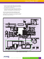
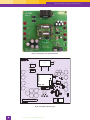
NEW
Product
ATC210 Dual Input Bus Converter
EVALUATION BOARD User Guide 207
1. Introduction
2
2. Evaluation Board Functionality
A_OK# and B_OK# LEDs
2
Converter Voltage LED
2
Clamp Voltage LED
2
Volt LED
2
3.3 Vout Margin Switch
2
Margin Switch Setting
2
12 V O/P Enable Switch
2
12 V LED
2
INTRPT LED
2
3. Connecting Up and interfacing the I2C Bus
207 Rev. 01 / 16 August 2006
File Name: an_atc210_evalbd.pdf
2
ATC210 Evaluation Board | User Guide 207
1. Introduction
The ATC210 Evaluation Board is designed to demonstrate the many
capabilities of Artesyn’s ATC210 converter. The ATC210 converter is
a high density, dual-input, dual-output, 210 W Bus Converter
designed to meet the requirements of the PICMG 3.0 Advanced TCA
Base Specification telecommunication standard. This converter is
designed to greatly simplify the power input requirements of the
ATCA system boards by integrating all the necessary components
(except hold-up capacitors) while operating on either of two isolated
-48 Volt power inputs and providing two low voltage (12 V and 3.3 V)
power outputs. Internally the ATCA converter contains, isolated
ORing diodes, a hot swap controller, a 41.5 V hold-up voltage clamp
to allow the use of small 50 V hold-up capacitors, an input
conducted EMI filter, highly efficient 12 Vdc and 3.3 Vdc converters,
a separate 12 V output switch, and a microcontroller based I2C
interface circuit.
The ATC210 converter offers a wide input voltage range of –36 Vdc
to -72 Vdc and can operate over an ambient temperature range of
-25 °C to +85 °C. Ultra-high efficiency operation is achieved through
the use of proprietary synchronous rectification and control
techniques. The module is fully protected against overcurrent,
overvoltage and overtemperature conditions. Standard features
include isolated remote ON/OFF, A_OK and B_OK power-good
indicators simplified 3.3 V margining, and I2C power and temperature
monitoring.
2. Evaluation Board Functionality
The evaluation board will function when an ATC210 converter is
either soldered or connected through pin sockets (jacks) to the
Evaluation Board, a voltage between -36 Vdc to –72 Vdc (valid
voltage) is applied to either –48V_A and RTN_A (“A” inputs), -48V_B
and RTN_B (“B” inputs), and both Enable_A and Enable_B are
switched on.
2.1 A_OK# and B_OK# LEDs
When Enable_A and Enable_B are switched on and a valid voltage is
applied to the “A” inputs, the A_OK# LED will light and likewise when
a valid voltage is applied to the ”B” inputs, B_OK# LED will light.
When a valid voltage is applied to both inputs, both LEDs will light.
In practice, the enable pins are the last to make contact. When they
do make contact, they connect to their respective Returns, and are
effectively the ‘green light’ for the ATCA power converter to start-up.
So, with both enables switched to the ‘on’ position, and with either
or both input feeds connected, the unit turns on.
2.2 Converter Voltage LED
The Converter Voltage LED will light when power is available to the
internal IBC -48 Vdc to 12 Vdc converter.
2.3 Clamp Voltage LED
When the input voltage on the hold-up capacitors rises to above 41
volts approximately, the Clamp Voltage LED will light to indicate that
the 50 V hold-up capacitors are charged to the minimum
requirement, to give a 5 ms hold-up time at maximum output load of
210 Watts.
2.4 3.3 Volt LED
The 3.3 V output LED will light when 3.3 V power is available at the
3.3 V output terminals. The 3.3 V output LED will not light if the 3.3 V
output voltage is less than 3.0 Volts. The 3.3 V output can drive up to
a maximum load of 1.8 A.
2
File Name: an_atc210_evalbd.pdf Rev: 16 Aug 2006
2.5 3.3 Vout Margin Switch
Once the 3.3 V power is available, the 3.3 V output voltage can be
increased or decreased by approximately 5% by switching the
margin switch either HIGH or LOW.
2.5.1 Margin Switch Setting
• High
3.3 V output = 3.47 V
3.3 V output = 3.32 V
• Normal
• Low
3.3 V output = 3.16 V
2.6 12 V O/P Enable Switch
This switch is effectively the remote control input. It is referenced to
the secondary side, and uses the 3.3 V output to enable/disable the
12 V output.
2.7 12 V LED
The 12 V output LED will light when the 12 V is switched ON and
power is available at the 12 V output terminals. The 12 V output LED
will not light if the 12 V output voltage is less than 11.3 V. The 12 V
output can drive up to a maximum load of 17.5 A including the 1 W
on board fan. The 12 V fan will operate when 12 V is available on the
12 V output. The fan can also be powered by an external 12 V
supply.
2.8 Interrupt LED
This LED will light whenever the interrupt line is active low. An
interrupt occurs whenever an internal parameter limit is violated. The
limits can be changed from the default values via the I2C bus.
3. Connecting Up and Interfacing the I2C Bus
This section describes in detail how to connect and install the
software.
The following list of items are supplied:
• Evaluation Board with ATC210 converter attached
• iPort/AFM RS-232 to I2C Bus Host Adaptor
• I2C Interface Cable
• RS-232 Serial Port Cable, 9F/25M
• Mains Power Supply
1. Download the ATC210 Evaluation Board Interface Program from
the Artesyn web site via the following link:
http://www.artesyn.com/registration/resource/ResourceProvi
der?target=/media/pdfs/atc210_sw_download.zip
2. Install the downloaded ATC210, there may be a need to load
Microsoft’s .Net Framework version 1.1. This software is
available via the following link:
http://www.microsoft.com/downloads/details.aspx?FamilyID
=262d25e3-f589-4842-8157-034d1e7cf3a3&displaylang=en
3. Connect the RS-232 cable between the iPort and the serial port
of the PC. If there is more than one serial port, the Interface
Program will connect automatically. The ‘pull-ups’ switch on the
iPort must be left in the default ‘off’ position when operating with
this Evaluation board. The iPort is manufactured by MCC, p/n
MIIC-203G, www.mcc-us.com.
4. Connect the I2C Interface Cable between the Evaluation board
and the iPort.
5. Plug the 5 V power supply into the ac outlet using the
appropriate Adaptor. Connect the other end to the iPort.
6. Double click on the ATC210 I2C icon that is on the desktop to
start the program.
User Guide 207
7. Power up the Evaluation Board. Make sure that both ENABLE
switches are in the ‘on’ position, and that the 12 V O/P switch is
also ‘on’. Operational voltage is between -36 Vdc and -72 Vdc.
Input voltage should not exceed 75 V.
8. Once powered up, the I2C communications can be initiated by
clicking on the ‘Connect II2’ button in the Interface Program. A
successful connection will indicate ‘iPort/AFM Found’ and ‘ATCA
Responding’ in the message box on the top right hand side.
Once the I2C communication has been established, the register
values and parameter values are read once and appear on the
interface. Reading or writing functions can be performed manually or
automatically. For more information on using the ATC210 Evaluation
Board Interface Program click on Help.
12V_OUT
FAN SUPPLY
EXT SUPPLY
S
E12
E11
J22
J21 INT SUPPLY
1 2
1 2
S
C4
1200UF
16V
20%
C3
1200UF
16V
20%
C5
1200UF
16V
20%
C6
1200UF
16V
20%
-48V_A E1
+
FAN
+
+
-48V_B E2
E14
E13
BNC2
C1
1UF
25V
10%
RTN_B E5
SW1
1 J6 -48V_A
1 J8 -48V_B
1 J9 EARLY_A
1 J10 EARLY_B
1 J11 RTN_A
1 J12 RTN_B
1 J19 ENA
1 J20 ENB
2
3
XXX
SW2 1
2
3
HU+OUT
XXX
D2
PDZ12B
XXX
S
S
C_CL-
S
R1
20K
1%
.25W
CR2
XXX
XXX
12V_RTN J5 1
1 J14 HU-
D1
C10 C11 C12
C9
C8
1000UF 1000UF 1000UF 1000UF 1000UF
50V 50V
50V 50V 50V
20% 20% 20% 20% 20%
+
+
+
+
R4 +
100K
1%
.125W
A2
S
S
R3
15K
1%
.25W
R2
15K
1%
.25W
A1
S
MMBD1404A
175V
CR3
XXX
XXX
C15
82UF
63V
20%
1 J16 ON/OFF1 J17 ON/OFF+
S
BSS63 C
12V_OUT J4 1
1 J13 C_CL-
E
B
R5
60.4 kΩ
1%
.125W
ATCA 210W
HU-
C_CL-
1 J7 HU+OUT
1 J15 HU+IN
S
R6
27.4 kΩ
1%
.125W
Q4
SW3
R2
5%
.5W
HU+OUT
3
3.3V_RTN
12V_RTN
C14
S C2 + 10UF
1UF
25V
25V
10% S 10%
R13
10K
1%
Q1 E
.125W
B
S
S
S
C
R12
R16 10K BSS63
S R15
13.3K 1%
681
1%
.125W
1%
.125W
VR2
.125W
AQT431
S R14
CR6
C16
XXX
1000UF 10K
XXX
1%
16V
20% .125W
S
SDA
S
SW4
3.3 V
O/P Adjust 1
2
OFF
3
XXX
J18 1
2
3
4
5
6
7
8
9
10
11
12
13
14
3V3_RTN
2
B_OK#
S
S
DEVICE=CON-MATE-14
R27
N/A
S
USB to SMBus
U5
DEL-COM IC
C23
10UF
10V
10%
S S
C24
100PF
100V
10%
P04
P00
P01
P05
P02
P06
P03
P07
P10
P11
P13
P12
D+
VSS
DVPP
VCC
CEXT
XTAL_OUT XTAL_IN
Y1
6 MHZ
S
R26
N/A
S
R28
N/A
3V3_RTN
R29
N/A
INTRPT
CR1
XXX
XXX
R11
681
1%
.125W
S
20
19
18
17
16
15
14
13
12
11
3V3_OUT
SCL
NOT ASSEMBLED
S
CR7
XXX
XXX
VR1
AQT431
R7
10K
1%
.125W
S
BNC4
C13
10UF
25V
10%
S
S
J1 1
2
3
4
C
R25
681
1%
.125W
BNC3
XXX
E16
.1W
1%
7.5K
R40
BSS63
R31
10K
1%
.125W
1 SW3
12 V R/C
HU-
USB
S
3.3V_OUT
Q5 E
B
S
BNC1
RTN_A E6
S
S
C7
1200UF
16V
20%
R10
80.6K
1%
.125W
R34
10K
1%
.125W
S
R33
1K
1%
.1W
2
3
4
5
6
7
8
9
10
R32
1K
1%
.1W
U1
PCA9515 8
Vcc
3 SDA0 SDA1 6
2 SCL0 SCL1 7
5 EN
NC 1
GND
S
R24
1K
1%
.1W
S
R17
10K
1%
Q2 E
.125W
B
S
R35
1K S
1%
.125W
S
R36
1K
1%
.125W
SDA
CR5
XXX
XXX
3V3_RTN
SDA
SCL
I C BUS REPEATER
3V3_RTN
R19
10K
1%
.125W Q3 E
B
SCL
S
R20 BSS63 C
10K
S
R22
1%
681
.125W
1%
.125W
B_OK#
S
C
R18 BSS63
10K
S R21
1%
681
.125W
1%
.125W
A_OK#
CR4
XXX
XXX
R30
1K
1%
.1W
3V3_RTN
S R8
S
I2C CONNECTOR
SCL
SDA
N/A
1 J2
2
3
4
4-PIN HEADER
SCL
SDA
INTRPT
1 J3
2
3
4
S R9
N/A
3V3_RTN
3V3_RTN
3V3_RTN
Figure 1: Evaluation Board Schematic
File Name: an_atc210_evalbd.pdf Rev: 16 Aug 2006
www.artesyn.com
3
ATC210 Evaluation Board | User Guide 207
Figure 2: Photograph of the Evaluation Board
ATC210W
EVALUATION BOARD
Ext Supply
Enable_A
OFF
Cooling Fan
Int 12 V
- +
ON
Airflow Direction
Enable_B
+
+
OFF
+
+
C4
C5
+
ON
UUT
J6
J9
-48 V_A
C1
C13
J8
TP2
J10
R7 R10
TP1
12 Vout
C7
C3
RTN_A
C6
BNC1 12 Vout
BNC2
VR1
J11
R25
J12
J19
J20
J14 J7 J15
J16 J17
TP4
Q4
R1
ON
C10
+353 24 93130
+1 800 769 7272
+852 2699 2868
R13
R12
VR2
C16
R14
R21
R27
3.3 Vout
R5
R32
TP6
CR4
CR5
A_OK
B_OK
3V3_RTN
INTRPT
SDA
SCL
Y1
CR1
INTERRUPT
J1
[email protected]
[email protected]
[email protected]
Figure 3: Evaluation Board Layout
File Name: an_atc210_evalbd.pdf Rev: 16 Aug 2006
U5
R40
3.3 V RTN
R33
C24
R24
R30 R9
CR3
CR2
C23
TP5
U1
WEBSITE www.artesyn.com
4
R16
BNC4
Q3
USB
EUROPE
NORTH AMERICA
ASIA
Q1
+
BNC3
NC
SDA
GND
+
C9
+
3.3 V
R15
Low Off High
SCL
C11
OFF
12 V O/P
C2
3.3 Vout
R22
TP7
CLAMP CONVERTER
VOLTAGE VOLTAGE
+
R18
R17
R19
R20
R4
R2
C12
C8
R11 Q2
SW3
Q1
R3
R23
+
C15
R5
R6
D2
C14
R26 R36
R28 R35
R29
J13
TP3
-48 V_B
12 V RTN
SW4
J18
RTN_B
12 V
3.3 V Trim
12C