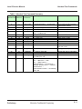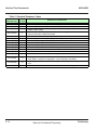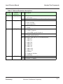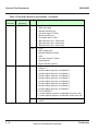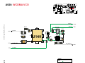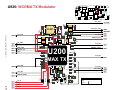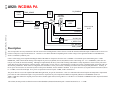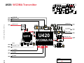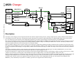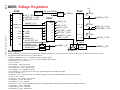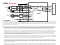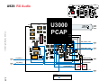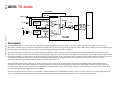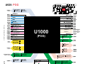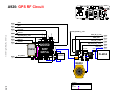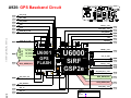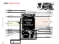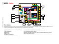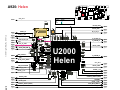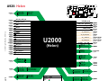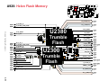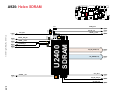
1
Level 3 Service Manual
Draft 1.1
™
DIGITAL WIRELESS TELEPHONE
Model A920/ A925
UMTS 2100MHz/ PCS 1900MHz/ DCS 1800MHz/ GSM 800MHz
Distribution Policy and Copyright
Copyright
© 2003 by Motorola. All rights reserved. No part of this publication may be reproduced, transmitted,
transcribed, stored in a retrieval system or translated into any language in any form by any means
without the written permission of Motorola.
Software License
The Agreement sets forth the license terms and conditions for using the enclosed Software. You may
use this Software on a single computer, and you may transfer it to another computer as long as it is
used on only one computer at a time. You may copy the Software for backup purposes only. You may
not rent, sell, lease, sublicense, time-share or lend the Software to a third party or otherwise transfer
this License without written consent of Motorola. You shall not decompile, disassemble, reverseengineer or modify the Software. This License is effective until terminated. You may terminate it at any
time by destroying the Software together with all copies. The License also terminates if you fail to
comply with the terms and conditions of this Agreement. United States copyright laws as well as
international treaty provisions protect this Software and accompanying documentation. Any use of the
Software in violation of these laws constitutes termination of the License.
Limited Liability
The Software and accompanying documentation is provided “AS IS” without warranty of any kind.
Motorola specifically disclaims all other warranties, expressed or implied, including but not limited to
implied warranties of merchantability and fitness for a particular purpose. With respect to the use of
this product, in no event shall Motorola be liable for any loss of profit or any other commercial damage,
including but not limited to special, incidental, consequential or other damages.
ii
Motorola Confidential Proprietary
Preliminary
Table of Contents
3G Flash Procedures ................................................................................................................. 1-1
Introduction ............................................................................................................................. 1-1
Hardware Requirements ......................................................................................................... 1-1
Power Solution ................................................................................................................................................ 1-1
Interface Solution ............................................................................................................................................ 1-1
PST Software .......................................................................................................................... 1-2
Flash Software Access ........................................................................................................... 1-2
Phone Flashing....................................................................................................................... 1-2
Power Solutions .............................................................................................................................................. 1-2
Hardware Connection Solution ......................................................................................................................... 1-2
Figure 1. PST Hardware Configuration ...................................................................................................... 1-3
PST Flash Procedure ...................................................................................................................................... 1-4
A920/A925 Special Procedures ....................................................................................................................... 1-5
Flash Procedure Summary ..................................................................................................... 1-5
Handset Test Commands ........................................................................................................... 2-1
Introduction ............................................................................................................................. 2-1
Application Installation* .......................................................................................................... 2-1
Figure 1. Launcher Menu ........................................................................................................................... 2-1
Figure 2. Install Window ............................................................................................................................ 2-1
Figure 3. Test Command Icon .................................................................................................................... 2-1
Handset Test Command Mode Entry ....................................................................................... 2-2
Figure 4. Password Prompt ....................................................................................................................... 2-2
Figure 5. Sub Applications ........................................................................................................................ 2-2
Figure 6. Main Entry Screen ..................................................................................................................... 2-2
Figure 6. Input Format ............................................................................................................................... 2-2
Entry Method ........................................................................................................................... 2-3
Opcode entry .................................................................................................................................................. 2-3
Figure 7. Fields entered Separately ........................................................................................................... 2-3
Entering Data .................................................................................................................................................. 2-3
Figure 8. Fields Entered with Delimiter ...................................................................................................... 2-3
Figure 9. Keyboard Entry ........................................................................................................................... 2-3
Figure 10. Stylus Entry ............................................................................................................................. 2-4
Figure 11. Invalid Entry ............................................................................................................................. 2-4
Result Screen ......................................................................................................................... 2-4
Figure 12. Results Screen ......................................................................................................................... 2-4
Table 1. Handset Test Command Summary ............................................................................................... 2-5
Table 2. Standard Response Codes .......................................................................................................... 2-6
Table 3. Field and Parameter descriptions ................................................................................................. 2-7
Table 3. Field and Parameter descriptions - continued ............................................................................... 2-8
Table 3. Field and Parameter descriptions - continued ............................................................................... 2-9
Preliminary
Motorola Confidential Proprietary
iii
Table of Contents
A920/A925
Table 3. Field and Parameter descriptions - continued ............................................................................. 2-10
Table 3. Field and Parameter descriptions - continued ............................................................................. 2-11
Manual Test Procedures ............................................................................................................ 3-1
Introduction ............................................................................................................................. 3-1
Call-Processing Tests ...................................................................................................................................... 3-1
Non-Signalling Test Measurements .................................................................................................................. 3-1
GSM/DCS/PCS Call Processing ............................................................................................ 3-2
Hardware Requirements .................................................................................................................................. 3-2
Software Requirements (PCS only) ................................................................................................................. 3-2
Call Origination (GSM and DCS only) .............................................................................................................. 3-3
Figure 10. GSM Signalling Setup .............................................................................................................. 3-3
Figure 11. GSM Connection Control .......................................................................................................... 3-3
Figure 12. GSM Call Connected ................................................................................................................ 3-3
Figure 13. A920 Manual Test Hardware Configuration ................................................................................ 3-4
Call Origination (PCS Only) ............................................................................................................................. 3-5
Figure 14. RadioComm COM Port ............................................................................................................. 3-5
Figure 15. Radio Comm Screen ................................................................................................................ 3-5
Call Test Parameters (GSM/DCS/PCS) ............................................................................................................ 3-6
Table 4. GSM Call Parameters .................................................................................................................. 3-6
Table 5. DCS Call Parameters ................................................................................................................... 3-6
Table 6. PCS Call Parameters ................................................................................................................... 3-6
Figure 16. Burst Output Shape .................................................................................................................. 3-6
Table 7. GSM/DCS/PCS Handover ............................................................................................................ 3-6
WCDMA Call Processing........................................................................................................ 3-7
Hardware Requirements .................................................................................................................................. 3-7
Software Requirements ................................................................................................................................... 3-7
Call Origination (WCDMA) ............................................................................................................................... 3-7
Figure 17. WCDMA Signalling Setup ......................................................................................................... 3-7
Figure 18. Channel Uplink(UE Signal) ........................................................................................................ 3-7
Figure 19. TPC Pattern Type(UE Signal) .................................................................................................... 3-8
Figure 20. WCDMA Call Connected ........................................................................................................... 3-8
WCDMA Call Test Parameters ......................................................................................................................... 3-8
Table 5. WCDMA Call Parameters ............................................................................................................. 3-8
Figure 21. WCDMA Modulation ................................................................................................................. 3-8
Figure 22. ACLR Screen ........................................................................................................................... 3-8
Non-Signalling Test Procedures (GSM/DCS/PCS) ................................................................. 3-9
Hardware Requirements .................................................................................................................................. 3-9
Software Requirements ................................................................................................................................... 3-9
Verify TX Power Output (GSM/DCS/PCS) ....................................................................................................... 3-9
Table 8. TX Power Limits ........................................................................................................................... 3-9
GSM RSSI .................................................................................................................................................... 3-10
Non-signalling Test Procedures (WCDMA) ........................................................................... 3-11
Hardware Requirements ................................................................................................................................ 3-11
Software Requirements ................................................................................................................................. 3-11
Verify TX Power Output (WCDMA) ................................................................................................................. 3-11
Table 9. WCDMA TX Power Output .......................................................................................................... 3-11
Audio/Vibrator Test Procedures............................................................................................. 3-12
Vibrator Test .................................................................................................................................................. 3-12
Handset Mic/Speaker test ............................................................................................................................. 3-13
iv
Motorola Confidential Proprietary
Preliminary
Level 3 Service Manual
Table of Contents
Mono Headset Mic/Speaker test ................................................................................................................... 3-13
Stereo Headset Mic/Speaker test .................................................................................................................. 3-14
Melody Speaker test ..................................................................................................................................... 3-14
Software Version Check ........................................................................................................ 3-15
Display Test Procedures ....................................................................................................... 3-15
Display Backlight Test ................................................................................................................................... 3-15
Display Color Test ......................................................................................................................................... 3-16
Figure 23. Eight Color Box Pattern .......................................................................................................... 3-16
Display Linearity Test .................................................................................................................................... 3-16
Figure 24. Grey Scale Block ................................................................................................................... 3-16
Display Flicker Test ....................................................................................................................................... 3-17
Figure 25. Zebra Pattern .......................................................................................................................... 3-17
Display Pixel Defect (Bright) ......................................................................................................................... 3-17
Display Pixel Defect (Dark) ........................................................................................................................... 3-17
LEDS and Keypad Backlight ................................................................................................. 3-18
Status LEDS ................................................................................................................................................. 3-18
Keypad Backlight .......................................................................................................................................... 3-18
Bluetooth Tests (V500/V600 only) ......................................................................................... 3-19
Unmodulated CW TX test .............................................................................................................................. 3-19
Camera Testing ..................................................................................................................... 3-20
Hardware Requirements ................................................................................................................................ 3-20
Camera Test Configuration ............................................................................................................................. 3-20
Figure 9. Camera Test Configuration ........................................................................................................ 3-21
Image Capture ............................................................................................................................................... 3-22
Macbeth Color Chart ..................................................................................................................................... 3-23
Focus Chart .................................................................................................................................................. 3-23
Grey Scale Chart (Shading Test) ................................................................................................................... 3-23
Service Diagrams ....................................................................................................................... 4-1
Introduction ............................................................................................................................. 4-1
Test Point Measurements ........................................................................................................ 4-1
Antenna Circuit ....................................................................................................................... 4-2
GSM Receiver Front End ........................................................................................................ 4-4
Magic LV (Receiver Back End) ............................................................................................... 4-6
Magic LV (Control) .................................................................................................................. 4-8
Magic LV (Synthesizer/Transmitter) ....................................................................................... 4-10
GSM TX VCO ........................................................................................................................ 4-12
GSM Transmitter .................................................................................................................... 4-14
WCDMA RX Front End ......................................................................................................... 4-16
WCDMA Receiver (MAX2309) ............................................................................................. 4-18
Harmony Lite (Receive Section) ........................................................................................... 4-20
Harmony Lite (Control Section) ............................................................................................. 4-22
Harmony Lite (Synthesizer Section) ...................................................................................... 4-24
Harmony Lite (Transmitter Section) ....................................................................................... 4-26
WCDMA VCO ....................................................................................................................... 4-28
WCDMA TX Modulator.......................................................................................................... 4-30
WCDMA Transmitter .............................................................................................................. 4-32
Prelimiary
Motorola Confidential Proprietary
v
Table of Contents
A920/A925
PCAP Charger ...................................................................................................................... 4-34
PCAP Regulators ................................................................................................................. 4-36
Receive Audio ...................................................................................................................... 4-38
Transmit Audio ...................................................................................................................... 4-40
PCAP .................................................................................................................................... 4-42
POG ...................................................................................................................................... 4-44
POG Interfaces ...................................................................................................................... 4-46
POG Memory ........................................................................................................................ 4-48
Bluetooth ............................................................................................................................... 4-50
GPS RF Circuit ..................................................................................................................... 4-52
GPS Baseband Circuit .......................................................................................................... 4-54
Video Circuit ......................................................................................................................... 4-56
Helen .................................................................................................................................... 4-58
Helen Interfaces .................................................................................................................... 4-60
Helen Flash Memory ............................................................................................................. 4-62
Helen SDRAM ...................................................................................................................... 4-64
SIM Connector ...................................................................................................................... 4-66
Battery Connector (J5400) .................................................................................................... 4-68
Camera Connector (J7600) ................................................................................................... 4-70
MMC Connector (J3900) ....................................................................................................... 4-72
Keyboard Connector (JPCH) ................................................................................................ 4-74
Display Connector (J5200) ................................................................................................... 4-76
CE Bus Connector (J5000) ................................................................................................... 4-78
Signal Flow Diagram (Side 1) ............................................................................................... 4-80
Signal Flow Diagram (Side 2) ............................................................................................... 4-81
RF Block Diagram ................................................................................................................ 4-82
Baseband Block Diagram ..................................................................................................... 4-83
Parts List ..................................................................................................................................... 5-1
Introduction ............................................................................................................................. 5-1
Electrical Parts List ................................................................................................................. 5-2
vi
Motorola Confidential Proprietary
Preliminary
3G Flash Procedures
Introduction
Hardware Requirements
This document is intended to describe the flashing (software updates) and procedures for 3G terminals. The
3G terminal described in this document will be limited
to the A920/A925.
The following hardware will be required to properly
flash the phone.
Software updates need to be handled in a controlled
manner. Carrier software approvals need to be considered before initializing a flashing procedure. Consult a
Motorola representative to ensure that the correct software is programmed.
1.
Fully Charged battery (SNN5638A)
2.
Full-rate Charger (PSM5049A)
Software updates allows the service organization to resolve field software issues that customers may be experiencing. Some issues may pertain to specific conditions, therefore, not all units will contain identical software versions.
1.
Power Solution
Interface Solution
USB PST Tool Kit (S8951)
USB Cable (SKN6311A)
Security Key
Adapter kit
Power supply (SPN4059A)
Motorola Confidential Proprietary
1-1
Flash Procedures
PST Software
Phone Flashing
The Product Support Tool (PST) is used to allow functions such as flashing, flexing, memory transfers, and
datalogging. Please contact your local Motorola service representative to obtain user documentation for the
PST.
Before beginning any flashing procedure, always insure
that all hardware connections are secured. Refer to figure 1 for flash connection guides. Any intermittent hardware connections may cause the procedure to fail and
result in a nonfunctional (Bricked) 3G terminal.
Insure that the Motorola service representative also provides installation documentation, security key requirements, and other related information.
The A920/A925 contains a set of Flash EPROMs for
the Adjunct Processor and a separate set of Flash
EPROMs for the Baseband Processor. Due to this design, the A920/A925 will require separate Flash files
for each processor if a “Combo” file is not provided.
Flash Software Access
A “Combo” file contains the following files,
Flash software can be accessed by Motorola personnel only. Contact your local Motorola service representative to obtain updated software releases.
In some cases the software may be distributed in ZIP
format. The user will need to extract the original (.SHX)
file from the ZIP file before is can be used with the PST.
WINZIP is the application that can be used to extract
the original flash file. For more information on WINZIP,
visit,
http://www.winzip.com
Adjunct Processor Flash
Baseband Processor Flash
Customer image flex
Power Solutions
There are two types of power solutions to perform a
flashing procedure.
1. Fully Charged Battery Solution
2. Full-Rate Charger Solution (recommended)
If the user decides on using the battery solution, he/she
must verify that the battery is fully charged. Failing to
verify the capacity of the battery may result in battery
depletion prior to completing the flash process. This
action may cause unrecoverable failures to the 3G terminal.
Hardware Connection Solution
A920 flash procedures require a USB hardware configuration. Refer to Figure 1 for details.
1-2
Motorola Confidential Proprietary
Flash Procedures
Figure 1. PST Hardware Configuration
PSM5049A
SKN6311A
Motorola Confidential Proprietary
1-3
Flash Procedures
PST Flash Procedure
7.
The 3G terminal will be placed in Adjunct flash
mode, select the device again to enable the Flash
button.
8.
Click on the Flash button to begin flashing. DO
NOT interrupt any hardware connections during the flash process. Connection interruptions
may cause the flashing process to fail and render the 3G terminal non-operational.
9.
When flashing is complete, a message will pop
up stating,” Flash another phone?”. Select “No”
and waiting for 30 seconds before continuing.
10.
Power up the 3G terminal to insure that the flash
procedure was successful.
11.
On the first power up, the user will be prompted
to select a language and calibrate the touch
screen.
Use the listed procedure to complete the flash procedure for a 3G terminal. The baseband processor needs
to be flashed first. Once the baseband processor flash
is successful, follow up with flashing the adjunct processor.
1.
Download the desired flash software into the
computer.
2.
Launch the PST application by choosing Start/
Programs/Motorola PST/Flash & Test Commands.
3.
Attach battery and connect hardware as illustrated in figure 1.
4.
Press the Power key and insure that the phone
is completely powered on.
5.
In the PST application, click on the Browse
button and select the desired flash software
6.
1-4
Select the device that will be flashed.
Motorola Confidential Proprietary
Flash Procedures
A920/A925 Special Procedures
Flash Procedure Summary
There are some variables that need to be considered
when updating software for a A920/A925. Improper
update procedures may cause the 3G terminal to fail.
Always read the release notes for software releases prior
to updating the software on a A920/A925.
The following is a summary of the procedures for flashing a A920.
The user needs to insure that the adjunct and baseband
flash files are part of the same build. Also, the user needs
to be aware of any step-up procedures. This may require the user to flash an updated bootloader. Step-up
procedures can be found in the software release notes.
In order to successfully flash a A920, the following sequence is recommended.
1. Backup user data
2. Flash/upgrade the software
3. Perform a “Master Clear”
4. Restore user data
1.
Launch PST.
2.
Connect USB hardware. Insure 3G terminal
remains off.
3.
Power up 3G terminal.
4.
Use the Browse button to open the “Combo”
flash file.
5.
Select the device for flashing.
6.
Select the device again to enable Flash.
7.
Click Flash.
8.
Click Yes to all the prompts if the user is certain
that software being flashed is correct.
9.
When flashing is completed, click “No” when
prompted, “Flash another phone?.”
10.
Power cycle phone. Verify functionality.
Motorola Confidential Proprietary
1-5
Flash Procedures
1-6
Motorola Confidential Proprietary
Handset Test
Commands
Introduction
The Handset Test Command mode of the phone is provided primarily for service personnel without access to
equipment capable of exercising Test Commands over
a computer connection. This mode collects input from
the user and packages it in the format required by the
Test Command component within the phone.
3.
The user will be prompt with a list of software
installation files.
4.
Highlight Test Command and select Install
Figure 2. Install Window
Application Installation*
The user needs to install the Handset Test Command
application before it can be accessed. Obtain the file,
“testcmdui.sis”, file from your local Motorola service
representative. Use the following procedure to properly install the handset test command application.
1.
Copy the testcmdui file into a memory card (SD
or MMC) and insure that the card is inserted in
the phone.
2.
From the App Launcher screen, select Install
from the Launcher drop down list
Figure 1. Launcher Menu
5.
When installation is complete, the Test Command icon will be displayed in the App Launcher
screen.
Figure 3. Test Command Icon
*Test application can only be loaded if application loading is not
secured.
Preliminary
Motorola Confidential Proprietary
2-1
Handset Test Commands
A920/A925
Command entry
Handset Test Command Mode
Entry
5.
Figure 6. Main Entry Screen
Follow these procedures to launch the handset test command aplication.
1.
Under the App Launcher screeen select the
Handset test command icon.
2.
The user will then be prompt to input a password
Choose Handset Test Commands to enter the
Test command Opcode screen
Figure 4. Password Prompt
6.
3.
The password is 0HTCMD#
Note: Password is case sensitive
4.
Once the application is launched, the user is
presented with a list of sub applications
Figure 5. Sub Applications
2-2
Before entering any commands, the user will
should select the data input format under the
Edit menu
Figure 6. Input Format
7.
The user can select Hexidecimal or decimal.
8.
Under the Edit menu, the user can also clear a
field or all fields
9.
The Back key will return the user to the App
Launcher screen
Motorola Confidential Proprietary
Preliminary
Level 3 Service Manual
Handset Test Commands
Command entry
Entry Method
The Back selection will clear the command contents
and return the user to the opcode prompt.
Once the test command mode is entered, two prompts
are used to collect command request information from
the user. The opcode entry prompt (Figure 5) allows
the entry of either an entire command as described in
this section, or entry of a partial command. If a partial
command is entered, the user will be prompted to enter
the remaining required information via an appropriate
number of field entry prompts (Figure 7). Selecting Test
with no data entered in the opcode or field entry screen
will cause a parse error (unless the field is optional).
If the user chooses to enter the entire command with
the necessary parameters in the Opcode prompt, “,”
delimiters will be used.
Figure 8. Fields Entered with Delimiter
The comma is used to delimit fields on the opcode entry prompt and is not allowed on the field entry prompt.
On the opcode entry prompt, it is not legal to have a
comma immediately follow another comma.
Opcode entry
The opcode entry prompt allows the user to enter the
opcode for the test command, or the opcode plus additional parameters delimited by the “,” character.
The user may select Test after entering the opcode. If
the opcode requires further parameters, the list of Fields
shall be shown starting with 1. After all the fields are
entered the user shall select Test. The results are then
shown on the screen.
Entering Data
When the User wants to enter the Fields, they shall click
the Keyboard Icon at the bottom of the screen to input
the values.
Figure 9. Keyboard Entry
Figure 7. Fields entered Separately
Preliminary
Motorola Confidential Proprietary
2-3
Handset Test Commands
A920/A925
Command Results
They can also use the Stylus, depending on the settings
selected by the user in the control panel.
Figure 10. Stylus Entry
If command processing takes more than 2 seconds a
message will display, “Running Test...”
Result Screen
The display of the output shall always be in Hexadecimal Format.
Figure 12. Results Screen
The user shall enter values in Hex or Decimal. The following values shall be allowed for each entry method:
•
•
Hex: A to F and 0 to 9. (not case sensitive)
Decimal: 0 to 9
When the user presses, "Test", the values shall be
checked whether they match the values that are allowed.
If not, they shall get an Error Message as follows:
Pressing the "Back" Key shall always take the user back
to the Main Entry Screen as shown in Figure 6
Figure 11. Invalid Entry
After the user presses, "Continue", they shall be taken
back to the field where the incorrect entry method was
found.
2-4
Motorola Confidential Proprietary
Preliminary
Level 3 Service Manual
Handset Test Commands
Table 1. Handset Test Command Summary
Opcode
Opcode
Hexadecimal Decimal
Opcode
Mnemonic
0
0
3
3
AUD_CTRL
4
5
6
4
5
6
AUD_LPB
AUD_LVL
AUD_PATH
7
0A
12
14
22
2D
36
7
10
18
20
34
45
54
37
55
39
3E
C0B
57
62
3083
C0E
3086
Preliminary
Key Entry Format
AUD_TN_LST 0 *<Action> * <Tone Identifier>OK
3 *<Device/Process> * <Action>OK
4 *<Loopback Type> * <Action>OK
5 *<Get/Set>*<Volume>OK
6 *<Input Path>*<Output Path>*<RX
Mute>*<TX Mute>OK
CARRIER
7 * <Option> * <Action> OK
CP_MODE
10 * <Set/Get> * <Sub-mode> OK
INVM
18 * <level> OK
LOAD_SYN 20 * <Channel> * 0 OK
RESTART
34 * OK
SET_RF_PW R 45 * <Power level> OK
SUSPEND
54 OK
Op Code Description
Generate/disable predefined tone
Control various audio functions;
enable/disable vibrator
Enable audio loopback
Set audio level
Change audio path
Enable GSM TX carrier
Set Call Processing Mode
Master clear or reset
Set GSM channel
Generate a software restart
Set GSM Power level
Terminate normal mode and
enter test mode
TST_DISP
55 * <Parameter> * <Parameter Data> Display predefined patterns
OK
VERSION
57 *<version Type>OK
Retrieve SW version information
LEDS
62 * <LED> * <Action> * <Data> OK
Control status LEDs
W LOAD_SYN 3083 * <RX_FREQ_ID> *
Set W CDMA channels
<TX_FREQ_ID> OK
W _CARRIER 3086 * <Channel ID> * <Action> * <Tx Enable W CDMA TX carrier
Pwr> * <Max Pwr> * <Min
Pwr> * <Data Pattern> *
<Channelization> * <Scrambling> *
<DPCCH Spread Factor> * <DPDCH
Spread Factor> *
<Channelization Code> * <Scrambling
Code> OK
Motorola Confidential Proprietary
2-5
Handset Test Commands
A920/A925
Table 2. Standard Response Codes
Opcode
Opcode
(Hexadecimal) (Decimal)
Response Field Definition
0000b (0x00)
0001b (0x01)
0
1
0010b (0x02)
2
0011b (0x03)
3
0100b (0x04)
0101b (0x05)
0110b (0x06)
0111b (0x07)
1000b (0x08)
1001b (0x09)
1010b (0x0A)
1011b (0x0B)
4
5
6
7
8
9
10
11
parse error (no data follows): invalid data length for command
parse error (no data follows): inadequate security level for command/parameter
parser error (no data follows): command/parameter not supported for current protocol
(CDMA, GSM, TDMA)
parse error (no data follows): command/parameter not supported for current mode
(normal, test mode, handset test mode)
parse error (no data follows): unsupported/invalid opcode
parse error (no data follows): unsupported/invalid parameter for opcode
command response: generic success (no data follows)
command response: generic failure (no data follows)
command response: data follows
unsolicited/multiple response: data follows (sequence tag is 0)
error: couldn’t allocate memory
error: internal task error
1100b (0x0C)
12
error: Test Command task timed out waiting for response from another SW component
1101b (0x0D)
13
1110b (0x0E)
14
1111b (0x0F)
15
2-6
CDMA: parse error (no data follows): command/parameter not supported for current submode TDMA: command not supported in current Call Stack Test Mode
error: length specified in command header greater than length received by transport
layer
error: irrecoverable error; phone state has been lost. Phone is being powered down
Motorola Confidential Proprietary
Preliminary
Level 3 Service Manual
Handset Test Commands
Table 3. Field and Parameter descriptions
Opcode
Opcode
Field Description
(Decimal)
Mnemonic
0
AUD_TN_LST Field 1 0 = stop a tone
1 = start a tone
Field 2 55 through 64 = DTMF tones, refer to table xx for more tones
3
AUD_CTRL Field 1 0 = Vibrator
2 = Echo canceling
3 = Noise suppressor
Field 2 0 = Disable
1 = Enable
4
AUD_LPB
Field 1 0 = PCAP loopback
6 = CODEC loopback
7 = VOCODER (speech) loopback
Field 2 0 = Disable Audio loopback
1 = Enable Audio loopback
Field 3 This field is valid only for VOCODER loopback
0 = AMR 4.75
1 = AMR 5.15
2 = AMR 5.90
3 = AMR 6.70
4 = AMR 7.40
5 = AMR 7.95
6 = AMR 10.20
7 = AMR 12.20
8 = Full Rate
16 = Enhanced Full Rate
32 = Half Rate
5
AUD_LVL
Field 1 0 = Set the volume specified
Field 2 0 = lowest, 7 = loudest
Preliminary
Motorola Confidential Proprietary
2-7
Handset Test Commands
A920/A925
Table 3. Field and Parameter descriptions - continued
Opcode
(Decimal)
6
7
2-8
Opcode
Mnemonic
AUD_PATH
CARRIER
Field Description
Field 1 0 = As is.
1 = Mute input path
2 = Internal (handset) mic
3 = Ext audio input (CE Bus)
4 = Boom (headset) mic
5 = Ext digital audio (USB)
7 = Bluetooth time slot 1 audio input
8 = Bluetooth time slot 2 audio input
9 = Bluetooth time slot 3 audio input
Field 2 0 = As is
1 = Mute output path
2 = Internal (handset) Speaker
3 = Alert
4 = Ext audio output (CE Bus)
5 = Speakerphone
6 = Boom (headset) speaker
Field 1 0 = All zeroes
1 = All ones
2 = pseudo random sequence w/midamble 0
3 = pseudo random sequence w/midamble 1
4 = pseudo random sequence w/midamble 2
5 = pseudo random sequence w/midamble 3
6 = pseudo random sequence w/midamble 4
7 = pseudo random sequence w/midamble 5
8 = pseudo random sequence w/midamble 6
9 = pseudo random sequence w/midamble 7
10 = RACH BURST
12 = pseudo random sequence w/midamble 0 two time slot
13 = pseudo random sequence w/midamble 0 three time slot
Field 2 0 = disable
1 = enable
Motorola Confidential Proprietary
Preliminary
Level 3 Service Manual
Handset Test Commands
Table 3. Field and Parameter descriptions - continued
Opcode
(Decimal)
10
18
20
34
45
54
55
Opcode
Mnemonic
CP_MODE
Field Description
Field 1 0=set submode
1=get submode
Field 2 5 = GSM 1900
6 = GSM dual band GSM900/GSM1800
8 = WCDMA Region 1
10 = Automatic - Dual mode: WCDMA region 1 and GSM
dual band GSM900/GSM1800.a
INVM
Field 1 0 = Master Reset
1 = Master Clear
LOAD_SYN Field 1 Channel number in decimal. Valid channel numbers are:
• 1-124 (PGSM 900 MHz)
• 0, 975-1023 (EGSM 900 MHz)
• 512-885 (DCS 1800 MHz)
• 512-810 (PCS 1900 MHz)
Field 2 Reserved for future use and TDMA; set to 0.
Field 1 As is
RESTART
SET_RF_PWR Field 1 PA power level (0-19)
Field 1 As is
SUSPEND
TST_DISP
Field 1 2 = Display Predefined Pattern
9 = Turn On/Off the Front Light
Field 2 Data for 2,
(Data) 000 = All pixels off (all black)
001 = All pixels on (all white)
005 = Grey scale block: 16 level, Black to white
006 = Horizontal Zebra Line
014 = Eight Color Box Pattern
Data for 9,
000 = Front Light Off
001 = Front Light On, Full Intensity
Preliminary
Motorola Confidential Proprietary
2-9
Handset Test Commands
A920/A925
Table 3. Field and Parameter descriptions - continued
Opcode
(Decimal)
57
62
3083
2 - 10
Opcode
Mnemonic
VERSION
Field Description
Field 1 016000 = DSP Version
017000 = User (login) pf process that created this file
017001 = Build time (universal) in ISO-8601 format
017002 = Clearcase view tag name
017003 = Product base label from Clearcase config spec
017004 = Product ID
017005 = Version Number
017006 = Build commentary
018000 = Flash Booter version number (P2K Booter Only)
Field 1 0 = Keypad Backlight LED
LEDS
3 = Red LED
4 = Green LED
Field 2 3 = Set duty cycle (Red/Green LEDS Only)
Field 3 Duty Cycle setup,
000 = Off
012 = ON
WLOAD_SYN Field 1 UARFCN for Receive Frequency ID. Valid values are
between 0 and 16383. If TX_FREQ_ID is set to 0xFFFF,
then RX_FREQ_ID must take values between 190*5 and
16383.
Note : If a valid TX_FREQ_ID will be entered,
RX_FREQ_ID must be set to FFFF.
Field 2 UARFCN for Transmit Frequency ID. Valid values are
between 0 and 16383. If it is set to 0xFFFF the TEST_TASK
will derive the TX_FREQ_ID from the RX_FREQ_ID.
Note : If a valid RX_FREQ_ID is entered, TX_FREQ_ID
must be set to FFFF.
Motorola Confidential Proprietary
Preliminary
Level 3 Service Manual
Handset Test Commands
Table 3. Field and Parameter descriptions - continued
Opcode
(Decimal)
3086
Preliminary
Opcode
Mnemonic
W_CARRIER
Field Description
Field 1 Channel identifier (0-16383).
Field 2 0 = Enable carrier.
1 = Disable carrier.
Field 3 Initial transmit power (dBm).
-128 dBm to 127 dBm
Field 4 Maximum transmit power (dBm).
-128 dBm to 127 dBm
Field 5 Minimum transmit power (dBm).
-128 dBm to 127 dBm
Field 6 0 = All 0s.
1 = All 1s.
2 = PN9.
3 = PN15.
Field 7 0 = Disable spreading.
1 = Enable spreading.
Field 8 0 = Disable scrambling.
1 = Enable long scrambling.
2 = Enable short scrambling.
Field 9 0 = SF256, slot format 0.
1 = SF256, slot format 1.
...
5 = SF256, slot format 5.
Field 100 = SF256, slot format 0.
1 = SF128, slot format 1.
...
6 = SF4, slot format 6.
Field 11Channelization Code Number.
Field 12Scrambling Code Number.
Motorola Confidential Proprietary
2 - 11
Handset Test Commands
2 - 12
A920/A925
Motorola Confidential Proprietary
Preliminary
Manual Test
Procedures
Introduction
Non-Signalling Test Measurements
The phone allows keypad and computer controlled testing of various digital test parameters.
In an event that the phone exhibits RF failures that prevent call processing, the service technician may need to
perform some non-signalling tests. These tests will provide information regarding which stage of the phone is
failing prior to opening the phone for troubleshooting.
The following tests will be described in this chapter.
This chapter includes the keypad/computer functions
and recommended equipment setup to use when testing a phone manually.
Call-Processing Tests
Most communications analyzers can simulate a cell site
in order to perform automatic call-processing tests.
Automatic call processing tests can be performed while
the phone is in standby mode.
Refer to the communications analyzer’s manual for details about performing call-processing tests. The following call-processing test sequence is recommended:
1.
2.
3.
4.
5.
GSM Mobile Originated Call
WCDMA Mobile Originated Call
GSM handover
DCS handover
PCS handover
Preliminary
•
•
•
GSM/DCS/PCS TX Power Output
GSM RSSI
WCDMA TX Power Output
The digital phasing parameters are stored in a EPROM
on the Transceiver Board. Each transceiver is shipped
from the factory with these parameters already calibrated. However, if a board is repaired, these parameters should be measured and, if necessary, adjusted
with the GP-Gate System. Checking and adjusting calibration parameters is also useful as a troubleshooting/
diagnostic tool to isolate defective assemblies.
Motolora Confidential Proprietary
3-1
Manual Test Procdures
A920/A925
GSM/DCS/PCS Call Processing
GSM/DCS/PCS Call Processing
RF Interface (Everything listed is required)
In order to successfully complete a GSM call processing procedure, a test USIM card needs to be available.
Test USIM cards have default call parameters that allow users to perform call processing tests through GSM
base station simulators. This allows service technicians
to perform simulations without accessing the customer’s
cellular account.
•
•
•
•
Hardware Requirements
If PCS call processing procedures are necessary, the
user will need to send a test command to the phone
prior to beginning the test. The command can be initiated through handset test commands or computer test
commands. Software requirements for each method is
listed below.
There are various hardware configurations to perform
manual call processing procedures. Below, is a list of
the various options. All options require the battery to
be attached. A GP-gate system can also be used for
manual testing. Refer to the GP-gate user’s manual for
details.
SMA/N-type Adapter (0-00-00-40042²)
SMA Cable 0.5m (0-00-00-40047²)
Repair Fixture (5-00-4T-10000²)
USIM (0-00-00-40810²)
Software Requirements (PCS only)
Handset Test Command
Power Options
•
•
Computer Test Command
Fully Charged Battery (SNN5639B¹ or equivalent)
•
Full-Rate Power Supply (PSM5049A¹)
•
Battery Eliminator (5-00-3F-10000²) with 2Wire Adapter (2-00-68-10000²)
Note: Requires a single output power supply
•
No software needed
Radio Comm (latest release)
Control Interface Options (PCS Only)
•
•
USB Cable (SKN6311A¹)
Serial Cable (SKN6315A¹) with CE converter
(SYN0279B¹)
Note: If handset test commands are being used, a control interface is not needed.
¹Contact your local Motorola dealer for ordering
²Contact AMS Software and Elektronik GmbH for ordering
3-2
Motorola Confidential Proprietary
Preliminary
Level 3 Service Manual
Manual Test Procedures
GSM/DCS/PCS Call Processing
Call Origination (GSM and DCS only)
Figure 11. GSM Connection Control
Use the following procedures for call processing. The
screen shots are from a Rohde and Schwarz CMU 200.
The procedures can be adopted to any other test box
that will be used to perform call processing.
1.
Install the test USIM in phone.
2.
GSM 900 Connection Control
Frequency
Offset
+0
Signal On
Single Slot
Hz
BCCH and TCH
Mode
BCCH
Level
- 85.0
RF
Channel
37
- 85.0
dBm
975
Ch. 2
GSM1900 Overview
Circuit
Switched
Single Slot
Connect
Control
Menu Select
Selection
GSM Mobile Station(GSM 1800/Signalling/Overview/P/t Normal GMSK
Basic Functions
GSM Mobile Station
GSM 850
GSM 900
GSM 1800
GSM 1900
3G UMTS User Equipment
WCDMA FDD
Non-Signalling
Signalling
4.
AUDIO
Analyzer/Generator
GSM 850
Analyzer/Generator
P/t Normal GMSK
GSM 850
Overview
P/t Normal GMSK
HotKeys
Set 1
Timeslot
Network
AF/RF
Sync
1
2
9.
Dial a number from the phone and press the
send button.
10.
The phone is now connected.
Figure 12. GSM Call Connected
HotKeys
Set 2
HotKeys
Set 3
GSM1800 Overview
Ch. 1
Ch. 2
RUN P/t Norm GMSK
1(28.0 dBm ) Reported Power
25.5 dBm Avg. Burst Power (Current)
25.7 dBm Peak Burst Power
Ok Power Ramp
- 0.75
RUN
Sym. Time Advance Error
Ext. Phase Error GMSK
- 30
6.2
2.1
HotKeys
Assign.
Frequency Error
Hz
Peak
Phase Error(Current)
RMS
MS Receiver Reports
Set Broadcast Channel (BCH) to 120 (GSM)
or 700 (DCS)
5.
Set Broadcast channel level to -85dBm
6.
Set Traffic Channel (TCH) to 38 (GSM) or 512
(DCS)
7.
Set Traffic channel level to -85dBm
Preliminary
Hopping
Overview
GSM 850
Overview
P/t Normal GMSK
Select
RF
Channel
MHz
Wait until the phone indicates a receive signal
Hotkeys - Set 1
GSM 850
Analyzer/Generator
P/t Normal GMSK
Menu
BS Signal
TCH
Level
8.
RF
Analyzer/Generator
Analyzer/Generator
MS Signal
1(28.0
Ch. 1
925.2
3
Connection
Figure 10. GSM Signalling Setup
dB
unused
Off
Note: Control interface doesn’t need to be connected at this time.
Setup up the test box for GSM or DCS Signalling
- 20.0
dBm
used
Connect hardware as illustrated in figure 13.
3.
Slot
Mode
17 (
0(
- 94 to - 93 dBm)
RX Level
0.0 to
RX Quality
Off
Discontinuous Transmission(DTX)
PCL
0.2 % )
Timing
Advance
Motorola Confidential Proprietary
Circuit
Switched
Single Slot
R P/t Norm,
U
N GMSK
Settings
Signalling States
MS Capabililties
Signalling Info
IMSI
IMEI
Dialled Number
Traffic Mode
Meas. Control
Repetition
Stop Condition
Display Mode
Statistic Count
Analyzer Level
RF Mode
RF Attenuation
Triiger Source
Trigger Slope
MS Signal
CIrcuit Switched
Timing Advance
Single Slot
PCL (MS)
Connect
Control
--- -------------123655
Full Rate Version 1
Continuous
None
Current
100 Bursts
Auto
Low Noise
Signalling
Rising Edge
Application
Analyzer
Level
MS Signal
BS Signal
Network
0 Sym.
1 (28.0 dBm)
Menus
3-3
Manual Test Procdures
A920/A925
Figure 13. A920 Manual Test Hardware Configuration
CMU200 Test Box
or Equivalent
SMA/N-type Adapter
0-00-00-40042
SMA Cable 0.5m
0-00-00-40047
Power Supply
(3.6Vdc, 2A)
2-Wire Adapter
2-00-68-10000
A920/A925
RF Fixture
2-00-4E-10000
A830 Battery Eliminator
5-00-3F-10000
P2K USB Cable
SKN6311A
Control Interface
Radio Comm equipped
Computer
3-4
RS232 to CE
SYN0279B
OR
Motorola Confidential Proprietary
P2K Serial Cable
SKN6315A
Preliminary
Level 3 Service Manual
Manual Test Procedures
GSM/DCS/PCS Call Processing
Call Origination (PCS Only)
•
Before beginning, one of the following test command
procedures needs to be completed.
Click on AT+/mode, suspend, CP_Mode 1900,
respectfully
Figure 15. Radio Comm Screen
Handset Test Command
•
•
•
Power up phone
Enter the following key sequence
Menu 0 H T C M D *
•
Enter the following test commands in the
Opcode screen
54 ok
SUSPEND
10*0*5
CPLOAD, GSM 1900
Power cycle phone
•
•
•
•
Power cycle phone
Repeat steps 1 through 10 in the ,“Call Origination
(GSM and DCS only),” section with the following modifications,
RadioComm Test Command
•
•
•
•
Connect as illustrated in figure 13
Power up phone
Start RadioComm application
Correctly select Settings option for USB or
serial
Figure 14. RadioComm COM Port
•
•
•
Set PCS Signalling
BCH = 661
TCH = 512
Once PCS call processing is complete, return the phone
to its original state by performing the following procedure,
Handset Test Command
•
•
•
54 ok
SUSPEND
10*0*10
CPLOAD, Dual mode
Power cycle phone
Computer Test Command (Radio Comm)
•
•
Preliminary
Click on AT+/mode, Suspend, CP_Mode 900/
1800, respectfully
Power cycle phone
Motorola Confidential Proprietary
3-5
Manual Test Procdures
A920/A925
GSM/DCS/PCS Call Processing
Call Test Parameters (GSM/DCS/PCS)
Burst Output Shape should fall within the standard limits of the Power Ramp.
While the phone under test is in an active call, the parameters for each band should be verified as described.
Table 4. GSM Call Parameters
Pa ra m e te r
Burst Avg Power Out¹
Burst Output Shape
Time Advance Error
RMS Phase Error
Peak Phase Error
Frequency Error
RX Level Error@-105 dBm²
RX Quality @-105 dBm²
BER @-105, 10k bits³
Low
Lim it
31
1
-1
0
-20
-90
1
0
0
High
Lim it
33
1
1
5
20
90
9
4
2
Unit
dBm
P/F
bit/sym
deg
deg
Hz
BER measurements is only required if RX Quality reads
a value of 4 or greater.
dB
%
High
Lim it
32
1
1
5
20
190
10
4
2
PCL:
---
1 / 28.0 dBm
/
Off
Chan. / Meas Slot:
740
/ 3
2:
--/
Off
Current
R P/t Norm,
U
N GMSK
Applic. 1
Applic. 2
Analyzer
Level
-20
-30
Ok
-50
25.57 dBm
- 0.75 Sym.
GSM 0
100 Bursts
-70
Unit
dBm
P/F
bit/sym
deg
deg
Hz
%
BS Signal
Avg.BurstPower(Cur.)
Timing Adv. Error
TSC detected
Network
Statiatical Counr
0.00 %
Out of Tolerance
60
80
Marker
0
20
Overview
Table 6. PCS Call Parameters
Low
Lim it
28
1
-1
0
-20
-190
2
0
0
Low Noise
1:
-60
¹Power Level = 0
²Set BS TCH level to -103 dBm
³Set BER TCH level to -103 dBm with 10k bits or 128 Frames
Pa ra m e te r
Burst Avg Power Out¹
Burst Output Shape
Time Advance Error
RMS Phase Error
Peak Phase Error
Frequency Error
RX Level Error@-104 dBm²
RX Quality @-104 dBm²
BER @-104, 10k bits³
Auto
/ Off
-10
-80
Pa ra m e te r
Burst Avg Power Out¹
Burst Output Shape
Time Advance Error
RMS Phase Error
Peak Phase Error
Frequency Error
RX Level Error@-103 dBm²
RX Quality @-103 dBm²
BER @-103, 10k bits³
Max. Level:
R:
---
+0
Connect
Control
MS Signal
Table 5. DCS Call Parameters
High
Lim it
32
1
1
5
20
180
11
4
2
Circuit
Switched
Single Slot
Ch. 2
-40
¹Power Level = 5
²Set BS TCH level to -105 dBm
³Set BER TCH level to -105 dBm with 10k bits or 128 Frames
Low
Lim it
28
1
-1
0
-20
-180
3
0
0
Figure 16. Burst Output Shape
GSM1800 Overview
Ch. 1
40
Power
Modulation
100
Spectrum
120
Display
140
Receiver
Quality
Audio
Menus
It is recommended that handover procedures be performed as shown in the following table.
Table 7. GSM/DCS/PCS Handover
Ba nd
GSM
DCS
PCS
From
Tra ffic
Pow e r
Cha nne l Control
975
5
512
0
512
0
To
Tra ffic
Cha nne l
124
885
810
Pow e r
Control
19
15
15
Unit
dBm
P/F
bit/sym
deg
deg
Hz
%
¹Power Level = 0
²Set BS TCH level to -104 dBm
³Set BER TCH level to -104 dBm with 10k bits or 128 Frames
3-6
Motorola Confidential Proprietary
Preliminary
Level 3 Service Manual
Manual Test Procedures
WCDMA Call Processing
WCDMA Call Processing
3.
In order to successfully complete a GSM call processing procedure, a test USIM card needs to be available.
Test USIM cards have default call parameters that allow users to perform call processing tests through GSM
base station simulators. This allows service technicians
perform simulations without accessing the customer’s
cellular account.
Setup up the test box for WCDMA FDD Signalling
Figure 17. WCDMA Signalling Setup
Ch. 1
Ch. 2
WCDMA FDD
Band
I
Connect
Control
Spectrum
Menu Select
Selection
GSM Mobile Station(GSM 1800/Signalling/Overview/P/t Normal GMSK
Basic Functions
GSM Mobile Station
GSM 850
GSM 900
GSM 1800
GSM 1900
3G UMTS User Equipment
WCDMA FDD
Hardware Requirements
Non-Signalling
Signalling
Hotkeys - Set 1
RF
Analyzer/Generator
Power
Spectrum
AUDIO
Analyzer/Generator
GSM 850
Analyzer/Generator
P/t Normal GMSK
GSM 850
Overview
P/t Normal GMSK
GSM 850
Analyzer/Generator
P/t Normal GMSK
Refer to , “Hardware requirements,” under, “GSM/
DCS/PCS Call Processing.” Also Refer to Figure 13.
GSM 850
Overview
P/t Normal GMSK
Menu
HotKeys
HotKeys
Set 1
Set 2
Select
HotKeys
Set 3
HotKeys
Assign.
Software Requirements
None.
4.
Set UE Signal, RF Channel Uplink to 9750
Figure 18. Channel Uplink(UE Signal)
Call Origination (WCDMA)
WCDMA FDD Connection Control
Signal On
Setup
Use the following procedures for call processing. The
screen shots are from a Rohde and Schwarz CMU 200
with WCDMA signalling options installed. The procedures can be adopted to any other test box that will be
used to perform call processing.
1.
Install the test USIM in phone.
2.
Connect hardware as illustrated in figure 4.
Analyzer Settings/RF Channel Uplink
Default All Settings
Analyzer Settings
RF Channel Uplink
Band [|]
Frequency Offset
RX/TX Separation
Measurement Settings
Default Settings
UL Scrambling Code
Analysis Mode
Sync. Mode
Measurement Slot Number
Correlatoin Mode
Threshold
UE Power Control
Default Settings
Connection
UE Signal
Channel
Frequency
Downlink
9750
1922.4 MHz
+ 0.000 kHz
190.000 MHz
2112.4 MHz
0
With Origin Offset
All Slots
0
DPCCH
- 25 dB
BS Signal
Network
RF
Sync.
1
2
Note: Control interface doesn’t need to be connected at this time.
Preliminary
Motorola Confidential Proprietary
3-7
Manual Test Procdures
A920/A925
WCDMA Call Processing
5.
WCDMA Call Test Parameters
Set TPC Pattern Type to All 1
Figure 19. TPC Pattern Type(UE Signal)
WCDMA FDD Connection Control
Signal On
Setup
TPC Settings/TPC Pattern Type
- 5.0 dB
3
- 3.0 dB
6
- 7.0 dB
6
0.0 dB
1
PICH
PICH Channel Code
AICH
AICH Channel Code
DPDCH
DPCH Channel Code
Power Offset (DPCCH/DPDH)
Secondary Scrambling Code
TPC Settings
Default Settings
TPC Algorithm
TPC Step Size
TPC Pattern Type
Pattern
Repeat Pattern
Connection
6.
UE Signal
Table 5. WCDMA Call Parameters
Network
RF
Sync.
1
2
Ch. 2
Dial a number from the phone and press the
send button.
WCDMA FDD
Band
I
Max. Level: + 30.0 dBm
Low Noise
Multiple Signal DPCCH+DPDCH 1
CCMode Manual
Scr Code 0
The phone is now connected.
RMS
Magn Error
Peak
RMS
Figure 20. WCDMA Call Connected
Ch. 2
WCDMA FDD
Band
I
Connect
Control
Power
Phase Error
Peak
RMS
I/Q Origin Offset
I/Q Imbalance
Carrier Frequency Error
Max. Level: + 30.0 dBm
Low Noise
Freq/Offset: + 0.000 kHz:
Chan. /Freq: 9750 / 1950 MHz
R Maximum
U
N Power
Application
Waveform Quality
Peak Code Dom Error
PCDE Code
UE Power (Peak)
UE Power (RMS)
24.77
24.02
Average
dBm
dBm
24.73
24.01
dBm
dBm
Maximum
24.94 dBm
24.09 dBm
Minimum
20.69 dBm
10
Statistic Count
Power
Application
Max /Min
22.16 %
8.80 %
14.03 %
5.52 %
12.47 °
3.95 °
- 32.95 dB
- 21.38 dB
4 Hz
0.99226
- 28.12 dB
26.5 %
10.2 %
15.3 %
5.6 %
15.4 °
4.9 °
- 32.37 dB
- 20.07 dB
- 76 Hz
0.9897
- 25.49 dB
I
0
Analyzer
Lev. Trigg
UE Signal
Ana. Set
0
Slot Number
20.81 dBm
UE Power
10
BS Signal
Level
Ch. 1
BS Signal
Settings
dBm
+40
Ch. 2
Modulation
Spectrum
Code Dom.
Power
WCDMA FDD
Max. Level: + 30.0 dBm
Freq. Offset: + 0.000 kHz
Band
I
+20
+10
Statistic Count
Overview
Power
Modulation
Spectrum
Low Noise
Connect
Control
R ACLR
U
N Filter
Chan. /Freq: 9750 / 1950 MHz
Current
640
Chip
Application
Meas. Length
- 10
----
- 20
UE Power
- 30
10
- 40
Statistic Count
- 50
-2
-1
0
- 10.00 MHz
- 5.00 MHz
- 47.4
- 55.7
- 34.9
- 41.5
- 55.7
- 45.1
- 55.2
- 41.5
- 34.6
- 41.3
Power
3-8
Menus
Receiver
Quality
+0
Menus
BS Signal
Settings
100.00 %
Spectrum
+30
100.00 %
Receiver
Quality
BS Signal
Level
Figure 22. ACLR Screen
Analyzer
Settings
Out of Tolerance
Code Dom.
Power
R Overview
U
N WCDMA
Chan. /Freq: 9750 / 1950 MHz
Out of Tolerance
Analyzer
Lev. Trigg
Current
Average
20.8 %
8.5 %
15.3 %
5.6 %
- 11.5 °
3.7 °
- 33.06 dB
- 21.74 dB
5 Hz
0.9929
- 29.11 dB
Q
1
Peak
Connect
Control
Modulation
Freq/Offset: + 0.000 kHz:
SR1 15
CC1 64
Current
Err Vect Magn
Ch. 1
Unit
dBm
Hz
%
dB
dB
dB
dB
Figure 21. WCDMA Modulation
Ch. 1
10.
High
Limit
21.5
195
13.5
-43
-33
-33
-43
¹Refer to Figure 10
²Refer to Figure 11
³Refer to Figure 12
Wait until the phone indicates a signal
9.
Low
Limit
20.5
-195
0
-100
-100
-100
-100
Parameter
Avg. RMS Power Out¹
Avg. Frequency Error²
Avg. RMS EVM²
Avg. RMS ACLR - 2³
Avg. RMS ACLR - 1³
Avg. RMS ACLR + 1³
Avg. RMS ACLR + 2³
Algorithm 2
1 dB
All 1
0000000000000000000000 bin
Off
BS Signal
While the phone under test is in an active call, the parameters for each band should be verified as described.
1
0 MHz
+ 24.7
+ 20.7
dBm
dBm
All
Values
in
dB
Modulation
Motorola Confidential Proprietary
2
Ch
100.00 %
Out of Tolerance
+ 5.00 MHz
+ 10.00 MHz
- 34.7
- 41.3
- 51.4
- 57.8
ACLR (Peak) Curr.
- 41.3
- 33.7
- 41.0
- 57.8
- 49.0
- 57.4
ACLR (RMS) Avg.
Spectrum
Code Dom.
Power
ACLR (RMS) Curr.
Analyzer
Lev. Trigg
Analyzer
Settings
BS Signal
Level
BS Signal
Settings
ACLR (Peak) Avg.
ACLR (RMS) Max.
Receiver
Quality
Menus
Preliminary
Level 3 Service Manual
Manual Test Procedures
Non-Signalling Test Procedures (GSM/DCS/PCS)
Non-Signalling Test Procedures
(GSM/DCS/PCS)
To perform non-signalling test procedures, the user is
required to be familiarized with sending test commands
to the phone under test. The test commands can be
sent using the Handset test command interface or
through a computer. Please refer to section, ”Handset
Test commands,” for details on how to send test commands through phone keypad entry.
In order to successfully send test commands to the phone
under test, the phone needs to be in suspend mode.
Follow the listed procedure to place the phone in suspend mode.
Handset Test Commands
54 ok
Handset Test Command
•
No software needed
Computer Test Command
•
Radio Comm (latest release)
Verify TX Power Output (GSM/DCS/PCS)
Verify the TX Power output by initiating the commands
in this section. Verify that the results fall within the following limits.
Table 8. TX Power Limits
Suspend
Parameter
GSM TX Power Out
DCS TX Power Out
PCS TX Power Out
Radio Comm Test Commands
Click AT+MODE then SUSPEND (Serial Only)
Click PST Initialize and click SUSPEND when initialization is complete
(USB Only)
Hardware Requirements
Refer to page 3-2 for a list of Hardware. Refer to Figure 13 for a configuration illustration.
Preliminary
Software Requirements
Low
Limit
31
28
28
High
Limit
33
29.5
29.5
Unit
dBm
dBm
dBm
Handset Test Commands
54
10*0*10¹
20*38*0²
45*5³
7*6*1
Suspend
WCDMA/GSM/DCS mode
Set Channel 38
Set GSM Power Level 5
Enable Carrier
¹10*0*5 for PCS mode
²20*700*0 for DCS Channel 700; 20*661*0 for PCS Channel 661
³45*0 for DCS/PCS Power level 0
Motorola Confidential Proprietary
3-9
Manual Test Procdures
A920/A925
Non-Signalling Test Procedures (GSM/DCS/PCS)
Radio Comm Test Commands
GSM RSSI
Click on 900/1800 (GSM/DCS) or
1900 (PCS)
Verify GSM RSSI by initiating the commands in this
section. Verify that the RSSI results are equal to the
Broadcast Channel (BCH) level. The user will need to
set the RF generator with the following parameters.
Enter 38 (GSM), 700 (DCS), or 661
(PCS) and then click Set
Broadcast Channel (BCH):
Broadcast Channel (BCH) Level:
20
-105 dBm
Handset Test Commands
No supported test commands
Enter 5 (GSM) or 0 (DCS/PCS)
and then click Set
Radio Comm Test Commands
Click on 900/1800 (GSM/DCS) or
1900 (PCS)
Select 06 and then
click ON
Enter Channel 20
Click INIT
Click Execute
Verify return data is approximately
-105 dBm
3 - 10
Motorola Confidential Proprietary
Preliminary
Level 3 Service Manual
Manual Test Procedures
Non-signalling Test Procedures (WCDMA)
Non-signalling Test Procedures
(WCDMA)
To perform non-signalling test procedures, the user is
required to be familiarized with sending test commands
to the phone under test. The test commands can be
sent using the Handset test command interface or
through a computer. Please refer to section,”Handset
Test commands,” for details on how to send test commands through phone keypad entry. Also, refer to,
“Computer Test Commands,” for details on how to send
test commands through the computer.
In order to successfully send test commands to the phone
under test, the phone needs to be in suspend mode.
Follow the listed procedure to place the phone in suspend mode.
Handset Test Commands
54 ok
Software Requirements
Handset Test Command
•
No software needed
Computer Test Command
•
Radio Comm (latest release)
Verify TX Power Output (WCDMA)
Verify the TX Power output by initiating the commands
in this section. Verify that the results fall within the following limits.
Table 9. WCDMA TX Power Output
Parameter
WCDMA Power Out
Low
Limit
20.5
High
Limit
21.5
Unit
dBm
Suspend
Radio Comm Test Commands
Handset Test Commands
Click AT+MODE then SUSPEND
(Serial Only)
Click PST Initialize and click SUSPEND when initialization is complete
(USB Only)
Hardware Requirements
Refer to page 2 for a list of Hardware. Refer to Figure
4 for a configuration illustration.
54
3086
Field 1
Field 2
Field 3
Field 4
Field 5
Field 6
Field 7
Field 8
Field 9
Field 10
Field 11
Field 12
9750
0
023
027
206
002
1
01
000
000
000
000000000
Suspend
W_CARRIER
Set Channel
Enable Carrier
Max Power Out
Max TX Power
Min TX power
PN9 Data pattern
Enable spreading
Long scrambling
SF256, Slot format 0
SF256, Slot format 0
Channelization Code
Scrambling Code
Note: Enter 1 in field 2 to disable carrier
Preliminary
Motorola Confidential Proprietary
3 - 11
Manual Test Procdures
A920/A925
Audio/Vibrator Test Procedures
Audio/Vibrator Test Procedures
Radio Comm Test Commands
This section describes how to use test commands to
verify audio and vibrate functions.
Click on WCDMA
In order to successfully send test commands to the phone
under test, the phone needs to be in suspend mode.
Follow the listed procedure to place the phone in suspend mode.
For W_CARRIER assign these actions to each field
Handset Test Commands
Freq ID (Dec)
Action
Channelization
Data Pattern
Scrambling
DPCCH
DPDCH
Channelization Code
Transmit Power
Max Power
Min Power
Scram Code
54 ok
9750
Enable
Enable
PN 9
Long
SF256, SF0
SF256, SF0
00
15¹
15¹
80²
00
¹0x0015 -> 21 dec -> +21dBm
²0x0080 -> 128 dec -> (128-256 = -128 dBm)
Suspend
Radio Comm Test Commands
Click AT+MODE then SUSPEND
(Serial Only)
Click PST Initialize and click SUSPEND when initialization is complete
(USB Only)
Vibrator Test
Handset Test Commands
3*0*1
3*0*0
Enable Vibrator
Disable Vibrator
Radio Comm Test Commands
Enable or Disable Vibrator
Verification
Verfiy vibration function when enabled.
3 - 12
Motorola Confidential Proprietary
Preliminary
Level 3 Service Manual
Manual Test Procedures
Audio/Vibrator Test Procedures
Handset Mic/Speaker test
Mono Headset Mic/Speaker test
Handset Test Commands
Handset Test Commands
6*2*2
4*7*1*16
6*4*6
Enable internal mic and handset speaker
Enable VOCODER loopback at Enhanced Full Rate
4*7*1*16
Enable headset mic and headset
speaker
Enable VOCODER loopback at Enhanced Full Rate
Radio Comm Test Commands
RadioComm Test Commands
Enable internal mic
and headset speaker
Enable headset mic
and headset speaker
Enable Vocoder loopback at
Enhanced Full Rate
Enable Vocoder loopback at
Enhanced Full Rate
Verification
Verification
Speak into the handset mic and listen for undistorted
speech in the handset speaker.
Preliminary
Speak into the headset mic and listen for undistorted
speech in the headset speaker.
Motorola Confidential Proprietary
3 - 13
Manual Test Procdures
A920/A925
Software Version Check
Stereo Headset Mic/Speaker test
Melody Speaker test
Handset Test Commands
Handset Test Commands
6*4*8
0*1*245
0*0*245
4*7*1*16
Enable headset mic and headset
speaker
Enable VOCODER loopback at Enhanced Full Rate
Play BACH_INVENTION_1
Stop BACH_INVENTION_1
NOTE: DO NOT issue a Suspend command (54 ok)
for this test.
RadioComm Test Commands
RadioComm Test Commands
Enable headset mic
and headset speaker
Currently not supported
Verification
Listen for undistorted audio.
Enable Vocoder loopback at
Enhanced Full Rate
Verification
Speak into the headset mic and listen for undistorted
speech in the headset speaker.
3 - 14
Motorola Confidential Proprietary
Preliminary
Level 3 Service Manual
Manual Test Procedures
Display Test Procedures
Software Version Check
Display Test Procedures
Use the following procedures to retrieve software information. Software information can also be retrieved
from the phone’s customer User Interface. Refer to the
phone’s user manual for details.
This section will describe the proper test procedures to
determine the functionality of the color display. Any tests
that involve displaying a predefined pattern can be returned to the Opcode screen by pressing the right softkey
of the phone.
In order to successfully send test commands to the phone
under test, the phone doesn’t need to be in suspend
mode. Follow the listed procedure to configure the
phone to accept test commands
In order to successfully send test commands to the phone
under test, the phone needs to be in suspend mode.
Follow the listed procedure to place the phone in suspend mode.
Handset Test Commands
Handset Test Commands
None
54 ok
Suspend
Radio Comm Test Commands
Radio Comm Test Commands
Click AT+MODE (Serial Only)
Click PST Initialize (USB Only)
Click AT+MODE then SUSPEND
(Serial Only)
Click PST Initialize and click SUSPEND when initialization is complete
(USB Only)
Test Commands
57*017003
57*017001
Read Software Version
Read Build Date
Display Backlight Test
RadioComm Test Commands
Handset Test Commands
Select Product Base
Label and click “Get”
to retrieve software
version
55*9*000
55*9*001
Backlight Off
Backlight On, full intensity
RadioComm Test Commands
Select Build Time
and click “Get” to retrieve Build Date
Click “FL Off” to disable backlight
Click “FL On-Full” to enable backlight
Verification
Verify that the backlights respond for each issued command.
Preliminary
Motorola Confidential Proprietary
3 - 15
Manual Test Procdures
A920/A925
Display Test Procedures
Display Color Test
Display Linearity Test
Handset Test Commands
Handset Test Commands
55*2*014
55*2*005
Eight Color Box Pattern
Grey Scale Block
RadioComm Test Commands
RadioComm Test Commands
Select Eight Color
Box and click “Set”
Select Grey Scale and
click “Set”
Verification
Verification
Verify that the color pattern on the phone’s display
matches the color box in figure 23. Also verify edges
(uniform/smooth).
Verify that the Grey scale block on the phone’s display
matches the Grey scale block in figure 14. This test can
also be used to confirm that the color intensity is linear.
Figure 23. Eight Color Box Pattern
3 - 16
Figure 24. Grey Scale Block
Motorola Confidential Proprietary
Preliminary
Level 3 Service Manual
Manual Test Procedures
Display Test Procedures
Display Flicker Test
Display Pixel Defect (Bright)
Handset Test Command
Handset Test Commands
55*2*006
55*2*001
Horizontal Zebra Line
All pixels on (all white)
RadioComm Test Commands
RadioComm Test Commands
Select Horizontal Zebra and click “Set”
Select All Pixels Off
and click “Set”
Verification
Verification
Verify that no noticable flicker exists.
Verify that no greater than two pixels are off.
Figure 25. Zebra Pattern
Display Pixel Defect (Dark)
Handset Test Commands
55*2*000
All pixels off (all black)
RadioComm Test Commands
Select All Pixels On
and click “Set”
Verification
Verify that no greater than two pixels are on.
Preliminary
Motorola Confidential Proprietary
3 - 17
Manual Test Procdures
A920/A925
LEDS and Keypad Backlight
Keypad Backlight
Use the following procedures to verify status LED and
keypad backlight.
Handset Test Commands
In order to successfully send test commands to the phone
under test, the phone doesn’t need to be in suspend
mode. Follow the listed procedure to configure the
phone to accept test commands.
62*0*1¹
62*0*0¹
Enable Keypad Backlight
Disable Keypad Backlight
¹Leave field 3 blank and press OK
RadioComm Test Commands
Select Keypad to enable. Deselect
Keypad to disable.
Handset Test Commands
None
Radio Comm Test Commands
Verification
Click AT+MODE then SUSPEND
(Serial Only)
Click PST Initialize and click SUSPEND when initialization is complete
(USB Only)
Verify that all keypad backlight LEDs activate.
Status LEDS
Handset Test Commands
62*3*3*012¹ Enable Red LED
62*4*3*012¹ Enable Green LED
¹000 to disable
RadioComm Test Commands
Select Red LED or Green LED to
enable. Deselect Red LED or
Green LED to disable.
Verification
Verify that the Red and Green status LEDS activate.
3 - 18
Motorola Confidential Proprietary
Preliminary
Level 3 Service Manual
Manual Test Procedures
Bluetooth Tests (V500/V600 only)
Under Bluetooth, select parameter 01 and enter
2DFC0129 in the “TO Radio” field. Click Execute.
Use the following procedures to verify functionality of
the Bluetooth device integrated in the phone.
In order to successfully send test commands to the phone
under test, the phone doesn’t need to be in suspend
mode. Follow the listed procedure to configure the
phone to accept test commands.
None
NOTE: The Bluetooth TX signal will activate momentarily once the HCI command is issued. You must have
the RF probe positioned for measurement once you
click execute.
Radio Comm Test Commands
Verification
Click AT+MODE then SUSPEND
(Serial Only)
Click PST Initialize and click SUSPEND when initialization is complete
(USB Only)
Verify that a 2441MHz signal is present. If the phone is
closed, use a RF probe to sniff the strongest signal
around the “7” key of the keypad. If the phone is open
(shields off), verify that -2dBm to +4dBm is read from
R320. An high impedance RF probe is required to read
this range. Use of lower quality RF probes will result in
signal level differences.
Handset Test Commands
Unmodulated CW TX test
Handset Test Commands
Not Supported
RadioComm Test Commands
Under Bluetooth, select parameter 84 and click execute,
then select 81 and click execute.
Preliminary
Motorola Confidential Proprietary
3 - 19
Manual Test Procdures
A920/A925
Camera Testing
Camera Test Configuration
This document is intended to describe the procedures
that will determine whether the camera function of a
Motorola terminal is under normal operating conditions.
Use any color printer to print a hardcopy of the Macbeth
color chart. The Focus chart and Grey chart can be
printed using any B/W printer.
In order to successfully send test commands to the phone
under test, the phone doesn’t need to be in suspend
mode. Follow the listed procedure to configure the
phone to accept test commands.
For best results follow this recommended setup,
1.
Attach chart to a flat vertical surface (wall)
2.
Attach the phone to the desktop charger
3.
Attach the control interface to desktop charger
4.
If necessary, attach power supply to control interface.
Click AT+MODE then SUSPEND
(Serial Only)
Click USB Initialize and click SUSPEND when initialization is complete
(USB Only)
5.
Turn on phone.
6.
Select Camera option in phone
7.
Position Desktop charger so that the camera
test chart completely fills the viewfinder.
Hardware Requirements
Assign a permanent space in the test lab for these test
procedures. Always use the same lighting conditions.
Also, it’s recommended that a “golden picture” is saved
and used for comparison.
Handset Test Commands
Not supported
Radio Comm Test Commands
The following hardware will be required to properly
test the camera function of the phone.
1.
Desktop Charger (SPN5032A or equivalent)
2.
USB or RS232 control interface (refer to figure 4)
3.
Fast Rate Charger (SPN5078A or equivalent)
4.
Hardcopy of Macbeth Color Chart
5.
Hardcopy of Focus Chart
6.
Hardcopy of Grey Chart
3 - 20
There is a variety of ways the camera test charts can be
attached to a vertical flat surface. They can be taped,
tacked, attached to flip charts, etc. Use your best judgement.
The desktop charger is being used as a fixture to position the phone for test, therefore, it’s recommended that
the desktop charger is attached to a countertop to prevent any movement.
Motorola Confidential Proprietary
Preliminary
Level 3 Service Manual
Manual Test Procedures
Figure 9. Camera Test Configuration
Camera Test
Charts
Phone under
Test
Camera
View
Charger
(SPN5049A)
USB
(SKN6311A)
Serial
(SYN0279B)
Desktop Charger
SPN5078A
To
Outlet
(110V/220V)
Preliminary
To
Computer
Velcro
(or equivalent)
Motorola Confidential Proprietary
3 - 21
Manual Test Procdures
A920/A925
Image Capture
Once the picture is captured, it’ll be displayed on the
screen. Click “Save To File”
The listed steps should be followed to capture three
images (1) the Macbeth color chart, (2) the focus chart,
and (3) the grey scale chart. The user will be required
to print all images found in Appendix A.
Handset Test Commands
Not supported
Radio Comm Test Commands
Under “Common Features” select Camera
Click “Take Picture”
3 - 22
Motorola Confidential Proprietary
Preliminary
Level 3 Service Manual
Manual Test Procedures
Macbeth Color Chart
Focus Chart
1.
From the computer, open the captured color
chart image.
1.
2.
Compare, the color blocks of the printed
Macbeth color chart to the captured image.
From the computer, open the captured focus
chart image.
Block 1-6
Block 7-12
Block 13-18
Verify the focus quality at the center, top-left corner,
bottom-left corner, top-right corner, and bottom-right
corner.
Block 19-24
Follow the listed verifications to determine the quality
of the image.
Grey Scale Chart (Shading Test)
1.
Minimal noise level for Blue, Green and Red
on blocks 19 through 24.
1.
2.
Uniformity for grey scale blocks 19 through 24.
3.
Good white balance on blocks 19 through 24.
4.
Good color reproduction on blocks 13 through
18.
From the computer, open the captured grey
scale chart image.
Verify that there is minimal shading deviations on all four
corners when compared to the center of the image.
Preliminary
Motorola Confidential Proprietary
3 - 23
Manual Test Procdures
3 - 24
A920/A925
Motorola Confidential Proprietary
Preliminary
Service
Diagrams
Introduction
The service diagrams were carefully prepared to allow
a Motorola certified technician to easily troubleshoot
cellular phone failures. Our professional staff provided
directional labels, color coded traces, measurement values and other guidelines to help a technician troubleshoot a cellular phone with speed and accuracy.
Because of the sensitivity of RF, measured readings will
be greatly affected if they’re taken in certain locations.
To get the most accurate readings, take measurements
nearest to the labeled measurement on the service diagram.
We worked hard in trying to provide the best service
diagrams, therefore, to avoid cluttered diagrams, we
may exclude some components from the service diagrams. Our professional staff carefully selected to excluded components that are unlikely to fail.
Test Point Measurements
The measurements labeled on the service diagrams are
approximate values and may vary slightly. These measurements are dependent on the accuracy of the test
equipment.
It is strongly recommended that the test equipment calibration schedule be followed as stated by the manufacturer. RF probes should be calibrated for each frequency
in which tests are going to be performed.
The types of probes used will also affect measurement
values. Test probes and cables should be tested for RF
losses and loose connections.
Preliminary
Motorola Confidential Proprietary
4-1
4-2
A920: Antenna Circuit
Int Antenna
M001
Ext Antenna
Ant
Match
WCDMA_RX
GSM_RX
GSM
RF SECTION
FL001
FEM
DCS_RX
PCS_RX
GSM_TX
DCS_PCS_TX
N_BAND_0_G
GSM_EXC_EN
Q902
Motorola Confidential Proprietary
N_GSM_EXC_EN
N_BAND_1
N_BAND_0
WCDMA
RF SECTION
FL030
CMOS level shifter
Decoder ASIC
RX_EN_LIFE
MAGIC
LV
WCDMA_TX
FL010
HARMONY
LITE
HL_TX_EN
GSM TX VCO
VRF_TX_2_775V
Description
POG
Q901
NB_EXC_EN
Q906
N_BAND_0
MAGIC LV
All cellular receive bands are fed into either the internal antenna or external antenna. M001 is a mechanical switch which has the internal antenna path connected when a
no insertion condition exists. The RF path will switch to external antenna upon insertion of a male SMA connector to M001. The internal antenna path is fed to the
FEM(Front End Module) through antenna matching components. The FEM provides band selection and filtering between the EGSM, DCS, PCS and WCDMA receive
and transmit bands to a single antenna port. GSM band selection is done by control lines N_BAND_1 and N_BAND_0_G. Mode selection is done by control lines
HL_TX_EN, RX_EN_LIFE, N_GSM_EXC_EN, and GSM_EXC_EN. The diplexing arrangement permits reception of WCDMA signals in any FEM switch position.
This allows the phone, while in a GSM call in any band, to detect signals from a WCDMA base station. The decision may then be made to hand over to the WCDMA
system. Similarly, EGSM base station signals can be detected while the phone is in a WCDMA call to permit a handover decision from WCDMA to EGSM (This is not
possible for base station signals in the DCS and PCS bands.).
Signals received at the antenna between 2110 - 2170MHz will see the RF switch as an open circuit at any position. Consequently WCDMA Rx signals will go through
FL2 to the WCDMA receiver. FL2 should have a maximum insertion loss of ~0.5dB. Outside of the WCDMA Rx band, FL2 behaves as an open circuit, preventing outof-band signals from reaching the WCDMA receiver.
GSM, DCS, and PCS receive signals from the antenna port through the FEM should have a maximum insertion loss of -4.4dB. The FEM EGSM transmit path should
have a maximum insertion loss of -2.5dB. The FEM DCS transmit path should have a maximum insertion loss of -3.1dB. The FEM PCS transmit path should have a
maximum insertion loss of -3.7dB.
Q902 is a dual FET package that’s being used to multiplex function of the N_BAND_0 control signal coming from the Magic LV. With the use of Q902,
N_GSM_EXC_EN will follow N_BAND_0. GSM_EXC_EN will be the inverted level of N_BAND_0. Q906 is another dual FET package that’s used to prevent simultaneous GSM and WCDMA transmission conditions. During WCDMA transmission conditions, HL_TX_EN will be in a high state. This will open both FETs in Q906,
thus, disabling any signal functions from control lines NB_EXC_EN and N_BAND_0. Q901 is used to invert the control signal coming from Q906.
A920: Antenna Circuit
N_BAND_0
page XX
page XX
U500
R912
Q906
R903
T650
T660
GSM_EXC_EN
GSM_RX
N_BAND_0_G
DCS_RX
page XX
T670
PCS_RX
RX_EN_LIFE
GSM_TX
FL001
page XX
L825
R812
page XX
Q902
page XX
E3601
page XX
FL001
page XX
FL001
page XX
N_BAND_0_G
Q906
page XX
N_GSM_EXC_EN
Q902
page XX
page XX
U810
N_GSM_EXC_EN
R900
N_BAND_0
page XX
page XX
VRF_HV_5V
R005
N_BAND_0_G
C902
GSM_EXC_EN
C004
Motorola Confidential Proprietary
FL001
HL_TX_EN
LV_EXC_EN
C003
U101
page XX
C903
page XX
page XX
Q902
NB_EXC_EN*
U500
DCS_PCS_TX
page XX
GSM_EXC_EN
HL_TX_EN
C006
U1000
C909
RX_EN_LIFE
N_BAND_1
C007
U101
HL_TX_EN
Q901
GSM_EXC_EN
Q902
page XX
HL_TX_EN
C010
C005
C030
U700
page XX
C008
page XX
VRF_TX_2_775V
U908
E3503
C908
page XX
R904
U1000
C910
TX_RX_ERROR
R901 R902
U500
page XX
U101
page XX
M001
ANTENNA
C002
page XX
Legend
Sig Gen:
RX:
TX:
-20dBm
FL030
WCDMA_TX
C460
4-3
4-4
A920: GSM RX Front End
GSM_RX
T650
RF
DET
DCS_RX
T660
RF
DET
PCS_RX
RX_Q+
RX_QRX_I+
RX_I-
U625
T670
LIFE
÷2
÷2 or 4
RX_EN_LIFE
÷5 or 3
Motorola Confidential Proprietary
AUX_SPI_CLK
AUX_SPI_DATA
MAGIC
LIFE_CE
LP
Filter
MAGIC
SPI
DCS
PCS
GSM
RX_VTUNE
RX_VCO
Description
The EGSM, PCS and DCS signals must first pass through baluns before reaching the LIFE IC. Since the LIFE expects differential inputs, the baluns will provide this.
Baluns provide the change from an unbalanced to a balanced line condition. By directly connecting to lines together, a possibility might arise where one line might
ground a signal and impair the operation of a circuit. This situation is solved through the use of an un-balanced to balanced transformer, a balun. Expected nominal losses is ~.5 - 1.0dBm.
The first IC in the EGSM, DCS, and PCS RX line up is U625 (LIFE), which is an LNA, VCO, and down converter mixer. The RX frequency is mixed down to a Very
Low Intermediate Frequency (VLIF) of ~ 100KHz. This design is utilized to improve LO leakage causing RF self-mixing, DC offsets, and noise performance. The LIFE
IC operates from the MAGIC_LV (tracking regulator), MAGIC_RF_V2_475. and MAGIC_SF (isolated supply for the VCO).
LIFE is comprised of four low noise amplifiers (three of which are used) with two quadrature mixer paths for use in receive GSM 900 (925- 960MHz), DCS (18051880MHz), and PCS (1930-1990MHz) frequency bands, all SPI programmable. The RX_VCO signal is fed back to the MAGIC_LV prescaler input. Although the frequency will be dependent of the channel selected, the amplitude signal is ~30dBm.
LIFE contains three fully contained VCOs which operate at ~4GHz. These VCOs are internally divided to provide precise quadrature down conversion for the three
frequency bands. The input signal RX_VTUNE from the RX backend processor (MAGIC_LV) selects the VCO frequency to operate at. The tune range is .5 - 4.5V.
The VCO frequencies for the three technologies are: DCS 3610 - 35759MHz, EGSM 3700 - 3838MHz, and PCS 3859 - 3980MHz.
The AGC is provided by a common amplifier section, which is shared by all four LNAs. The AGC amplifier gain control is controlled by the voltage on the AGC pin,
utilizing the internal 6-bit D/A to set the AGC via the SPI lines (SPIDATA, SPI_CLK, and SPI_CE). LIFE has an internal RF detector at the input of the AGC amplifier.
The detected DC output level will be compared against a reference, which corresponds to the maximum safe input level to the mixer. This reference is SPI selectable so
that the threshold can be set to 0dB, 3dB, 6dB, or 9dB below the level, which results in the mixer malfunction. If the detected level is above the reference then
AGC_FLAG will go high. The MAGIC_LV will receive this signal as an interrupt and will reprogram the AGC until the level drops below the safe mixer input level as
signified by AGC_FLAG returning low.
The output signals I / IX and Q / QX are @ ~100KHz IF value for the Very Low IF. The input pin, RX_EN_LIFE controls the on / off state of the receiver and the PLL
circuits. For input amplitude at the antenna of -50 to -40dBm the expected nominal output should be an AC rms peak-to-peak voltage of ~4.5 - 14mV.
A920: GSM Receiver Front End
C537
MAGIC_SF
page XX
RX_I+
E3552
page XX
U500
R508
page XX
U630
RX_VCO
VLIFE
U500
RX_QRX_VTUNE
page XX
Legend
Sig Gen:
RX:
VCO:
C605
C504
C503
R615
-20dBm
PCS_RX
FL001
AGC
C670
T670
DCS_RX
FL001
page XX
C660
T660
GSM_RX
C650
C651
FL001
page XX
T650
E530
C505
R503
AUX_SPI_DATA
R504
page XX
U500
C604
C608
C610
page XX
C600
U600
LIFE
C609
page XX
RX_Q+
L610
C607
U500
R611
page XX
C632
L3560
C671
C661
VLIFE
page XX
VRF_RX_2_775V
TP601
C606
U630
RX_I-
page XX
U500
R610
page XX
VRF_REF_2_475V
C603
page XX
VRF_RX_2_775V
R612
Motorola Confidential Proprietary
L3560
C602
C631
U500
page XX
AUX_SPI_BUS
U500
page XX
4-5
4-6
A920: GSM RX Back End (Magic LV)
RX_I
RX_I_X
IFA
Σ∆
RX_Q_X
Filter
Balanced
Complex
Mod
DET
PMA
IFA
AntiAliasing
filter
Motorola Confidential Proprietary
MAGIC LV
U500
(RX Section)
Σ∆
Filter
Prgmable
Dig CH Sel
and
Complex
IF Notch
or
Highpass
BFSR
RX
Serial
Interface
BDR
NB_RX_ACQ
POG
DET_FLAG
RX_Q
Description
AntiAliasing
filter
FL500
GSM
RX
Front End
PMA
BCLKR
Dig Quad
Osc
The MAGIC_LV (U500) handles the backend processing for the EGSM, DCS and PCS (VLIF: RX_I, RX_I_X, RX_Q, and RX_Q_X) signal lines from LIFE. Simply,
the MAGIC_LV performs an analog to digital conversion of I /Q and sends it to the data to the board processor (POG) via the SSI (serial synchronous interface).
The MAGIC_LV also has a programmable and phase-able digital IF to improve image rejection.
In MAGICLV, each channel is comprised of a Post Mixer Amplifier (PMA), an integrated passive two pole filter, a gain stage (AMP1) followed by an active programmable 2 pole anti-aliasing filter (mainly required to meet the blocking specs). This is followed by a lowpass sigma-delta ADC with a programmable oversampling clock
OVSCLK (derived from the reference oscillator) equal to 13MHz for 200kHz channel spacing (13bits).
Digital detector circuits are placed on each channel at the output of the sigma delta converters. The outputs of these detectors are compared against a level defined by
DET_LVL. If either of the detected levels exceeds the programmed threshold then the pin DET_FLAG is set high. This indicates that the signal level is excessively high
for the sigma delta modulator. DET_FLAG is read by the processor, which will respond by re-programming one of the AGC settings to a lower gain until DET_FLAG
returns low.
The outputs of the sigma-delta modulators are digitally processed through a noise cancellation circuit, comb and decimation filters. A second programmable digital LO
based on a look up ROM generates digital quadrature oscillators with programmable gain/phase correction (called balanced complex multiplier) to digitally downconvert
the I/Q signals to baseband (digital zero IF) through four quadrature mixers that provide image rejection of adjacent/alternate channels. Gain/ Phase correction at a single
baseband frequency is performed on the Digital Quadrature Oscillator to compensate the analog gain/phase mismatch of the quadrature I and Q paths. After baseband
downconversion and image reduction, the quadrature I and Q signals are further processed by digital filters that perform channel selectivity and out of band noise rejection.
A serial bus consisting of SDFS and SDRX will transmit the RXI and RXQ data in 2‘s complement format. BDR and BFSR are outputs from MAGIC LV. BFSR is a
framing signal which marks the beginning of an I,Q transfer. BDR is the serial data. The clock used for the serial transfer is BCLKR. When NB_RX_ACQ goes high
MAGIC LV will activate the SSI interface in the digital receiver section. The data transmission over the serial bus will begin at the next normal occurrence of valid I and
Q data, as defined internally to the digital receiver.
A920: Magic LV (Receiver Back End)
Motorola Confidential Proprietary
U500
MAGIC LV
C540
C534
E975
Y500
C542
TP504
U1000
NB_RX_ACQ
page XX
U1000
page XX
U1000
page XX
4-7
U1000
page XX
BFSR
BDR
BCLKR
FL500
E977
FL510
R537
R536
RX_I+
U600
page XX
RX_I-
U600
page XX
RX_Q+
U600
page XX
RX_Q-
U600
page XX
4-8
A920: MAGIC LV Control Functions
RF_TOP
MAGIC LV
U500
(Control)
N_BAND_1
N_BAND_0
TX_KEYM
80 bit
Serial
Reg
MAGIC_DX
MAGIC_SPICLK
LIFE
AUX_SPI_CLK
AUX_SPI_DX
LIFE_CE
T X C o n t ro lle r
POG
Aux
SPI
Cntrl
R A M P C o n tr o lle r
AOC
Filter
MAGIC_SPI_CS
Σ
DET_AOC
DET_REF
GSM
TX
VRF_RX_2_775V
VRF_REF_2_475V
VRF_REF_2_475V
V5
Superfilter
V2
R F _ V 2 _ 2 _ 4 7 5 V
S F _ O U T
R F _ V 5 _ 2 _ 4 7 5 V
MAGIC_DIG_1_875V
V4
R F _ V 4 _ 1 _ 8 7 5 V
VRF_DIG_1_875V
R F _ V 3 _ 1 _ 8 7 5 V
Motorola Confidential Proprietary
V3
Description
AOC_DRIVE
The MAGIC LV contains 4 tracking regulators and one superfilter, which will generate the supplies for most of the IC as well as the front end and the main VCO. The
tracking regulators derive their internal power from the REG_REF pins. The reference voltages are filtered and buffered for use on the IC. The buffered voltages should
track the references within +/-1.5%. A raw supply voltage is provided to the tracking regulators which is higher than REG_REF as specified below for each regulator. A
superfilter is needed for the external VCO power supply. This superfilter, cascaded with an external regulator and any filtering in front of the IC, will need to provide
80dB of rejection to a 0.1V step occurring at a 217Hz rate with a risetime of 20us on the raw supply (battery) and a duty cycle of 0.125. The superfilter will use an internal pass transistor that is capable of driving a 30 mA load with a voltage drop of less than 0.4V relative to SF_SPLY from the SF_OUT pin. An external 1uf cap is
required on SF_OUT. As the superfilter will track SF_SPLY it will need to sense the power on reset and turn off even though its supply may remain active. All supplies
within the IC must be within 5% of their final values after 5msec from the start of POR_LB. The power on reset circuit contained within the crystal reference oscillator is
used to aid this functionality.
The MAGIC_LV has two sets of SPI interfaces; one set is for handling the control interface for the LIFE IC (AUXSPI lines) and ones for interfacing with POG (SPI
lines). AUX_SPI_DX is the serial data input line. AUX_SPI_CLK is the clock input line, where data shifting occurs at the rising edge of this signal. LIFE_CE is the
clock enable line, active high, for the LIFE IC.
MAGIC_LV will integrate a system of D/As and control logic to generate the power amplifier control ramps. In addition, MAGIC_LV will integrate the op-amps and
comparators which receive the detected output of the power amplifier and create the necessary control voltage to drive the power amplifier control port based on the control ramps. When TX_KEYM goes high, the ramp controller receives an positive input. This will cause the AOC_DRIVE pin to linearly rise which in turn will cause the
PA output power to rise. The rising PA output power will cause DET_AOC to begin to rise until the DC level on DET_AOC exceeds the DC level on DET_REF by the
intentional offset of the RF detector versus it‘s reference. At this point the “Active Detect” comparator will go low and break the input voltage to the integrator with the
ramp controller. This will cause the PA power to stop rising and hold the present power level as determined by the 8 bit offset value fed to the ramp controller. The PA
control loop is now at a minimal power needed to keep the control system in a closed loop for a controlled ramp up of the power.
The MAGIC uses two SPI driven GPO lines which are used to control the operating bands of the GSM RF circuits. They are N_BAND_0 and N_BAND_1.
When the MAGIC LV is set to battery save mode it will shutdown the receiver analog sectioins (via RX_EN_LIFE), the AOC, the main synthesizer and the superfilter.
A920: Magic LV (Control)
C521
VRF_V3_1_875V
TP500
C536
TP502
RF_V4_1_875V
page XX
U510
C546
MAGIC_SF
C538
page XX page XX
C537
U7704,C603
MAGIC_REG_REF_1_875V
C522
C514
page XX
VRF_REF_2_475V
C523
page XX
C506
E3552
Q510
R511
C560
R508
VRF_DIG_1_875V
VRF_REF_1_875V_OUT
LIFE_CE
E528
C3250
page XX
U600
C516
page XX
MAGIC_REG_REF_1_875V
C510
U630
L3560
page XX
U510
C521
page XX
C514
C517
VRF_V3_1_875V
VRF_REF_2_475V
C506
page XX
E3552
page XX
RF_V4_1_875V
C522
page XX
C546
C520
Motorola Confidential Proprietary
VLIFE
VRF_RX_2_775V
C524
MAGIC LV
E3951
page XX
page XX
C539
U500
C542
page XX
R3251
page XX
MAGIC_DIG_1_875V
VRF_REF_2_475V
E3552
page XX
TP504
C545
C543
FL510
E529
NB_SPI_CLK
page XX
C511
U1000
TP501
C544
C540
E976
E975
C534
C542
AUX_SPI_CLK
page XX
4-9
U1000
page XX
E977
R537
R536
C525
NB_SPI_MOSI
MAGIC_CS
U600
U1000
page XX
4-10
A920: MAGIC LV (Synthesizers/Transmitter)
RX_VCO
PRSC
TX_VCO_PRSC
Mod_sel
TX
VCO
CP_TX
Ø
3 Acc
FN Seq
Gen
RX_VTUNE
LIFE
Σ
GSM
Look-up
Table
TXCLK
GSM
Pre-Distort
TX Data
Interface
DMCS_MAGIC
SDTX
BFSX
Y500
POG
AMPS
Interpolator
Motorola Confidential Proprietary
CLK_SEL
BB_CLK_13M
Description
MAGIC LV
U500
(Synthesizer Section)
3 Acc
FN Seq
Gen
Σ
FL510
Ø
PLL_CP
The MAGIC_LV receives SSI Tx data at DMCS (digital input to start Tx modulation), TXCLK (clock for serial transfer) and SDTX ( serial Tx data) from POG. The
present serial data bit and the three previous data bits are used to set up one of 16 possible waveforms based on the sum of Gaussian pulses stored in a look up ROM.
The resulting signal will then be clocked out at a 16x over-sampling rate. This data pattern input to three-accumumalator fractional N synthesizer with a 24-bit resolution. The VCO control lines must have compliance over an output voltage range of 0.3VDC to Vcc-0.3V. The charge pumps will have their own supply pin. The voltage
on this pin is expected to be 2.775V typically to obtain sufficient compliance. This will drive external loop filters, which will in turn drive external VCOs. A dual port
modulation mode is obtained with a 9 bit D/A which follows the modulation look up table output waveform is output on the GPO3 pin.This signal is then coupled into
the loop filter to add in the higher frequency components of the modulation which may have been attenuated in the main PLL path. This will allow the use of a lower
bandwidth main PLL to improve the spectral purity of the transmit signal.For EGSM the synthesizer output is 880 - 915MHz, DCS is 1710 - 1785MHz with GMSK modulation and is directly amplified to the transmitter output.
The prescaler for the main LO is able to accept input frequencies as high as 2.0GHz. The level of this signal shall be between -20dbm and -10dbm. There are two
prescaler inputs to this point each has a 100W resistor in series between the pin and the actual prescaler input.
The reference oscillator is a free running 26MHz crystal. AFC is provided through the SPI bus as a programming offset to the fractional N division system. Since the
26MHz crystal is not locked to the AFC, a second fractional divider system is necessary to derive an accurate 200KHz system reference. This reference is then multiplied
in a PLL to 13MHz for use as an accurate clock to the logic sections of the transceiver.
A920: Magic LV (Synthesizer/Transmitter)
VRF_RX_2_775V
page XX
VRF_HV_5V
page XX
NB_TX_KEYM
C509
page XX
R508
R556
BFSX
E528
C556
R506
page XX
C554
R554
R526
C526
Q510
U500
C528
DMCS_MAGIC
C510
C514
page XX
U600
page XX
U1000
U1000
page XX
C517
TX_CLK
C546
SDTX
U1000
page XX
U1000
page XX
VRF_REF_2_475V
E3552
page XX
TP504
C534
C542
E975
Y500
page XX
C540
FL510
R537
Legend
4-11
Sig Gen: -20dBm
Ref. Freq:
VCO:
U630
page XX
VRF_RX_2_775V
page XX
VLIFE
C525
L3560
U1000
page XX
C524
MAGIC LV
C527
MAGIC_DIG_1_875V
C539
PLLBASE
R807
AOC_DRIVE
VCORNG
Motorola Confidential Proprietary
C555
PLLEMIT
DET_AOC
page XX
PLLCP
R810
RX_VCO
C516
PRSCINT
C521
U710
C502
C520
E3601
C507
C535
L3560
R536
BB_CLK_13M
U1000
page XX
CLK_SEL
U1000
page XX
4-12
A920: GSM TX VCO
RF_TOP
Section
GSM_EXC_EN
N_GSM_EXC_EN
NB_TX_EN
POG
U700
TXVCO
Q700
Decoder
N_BAND_0
GSM VCO
N_BAND_1
GMSK
Look-up
Table
9 bit
Dual Port
D/A
Mux
Delay
FN
CP_TX
Loop
Filter
TX_VCO_HB
Tank
Ckt
GPO3
Motorola Confidential Proprietary
TX_VCO_PRSC
SF_OUT
Pre-dist
Sys
TX_VCO_LB
DCS/PCS VCO
MAGIC LV
Description
The VCO frequencies are 897 - 1880MHz, handling the three technology bands. The technology bands are controlled by MAGIC_LV via the data lines: N_BAND_0 and
N_BAND_1. CP_TX and GPO3 provides a dual port modulation mode for the TXVCO. N_BAND_0 and N_BAND_1 will select which VCO band will be activated.
GSM_EXC_EN and N_GSM_EXC_EN will enable the buffer stage of U570. TX_EN is activated prior to enabling the buffer and PA. TX_VCO_PRSC is fed back to the
MAGICLV for proper PLL operation. The output frequency for GSM is TX_VCO_LB and PCS / DCS is TX_VCO_HB. The charge pump output (CPTX) from
MAGIC_LV is the input (VT) for the VCO.
A920: GSM TX VCO
N_BAND_0
N_BAND_1
U500
page XX
U500
page XX
N_GSM_EXC_EN
L701
U1000
C700
C712
MAGIC_SF
C711
C708
C701
page XX
C706
TX_VCO_LB
U800
page XX
R700
GSM
TX VCO
C703
Q700
NB_TX_EN
page XX
C537
U700
R703
TX_VCO_HB
C707
C702
page XX
C713
C701
R704
CPTX
page XX
C5576
U500
C710
Q902
U710
L710
GPO3
page XX
R705
Motorola Confidential Proprietary
U500
C704
R577
R576
C705
L703
PRSCINT
C509
page XX
page XX
GSM_EXC_EN
Q902
page XX
Legend
Sig Gen:
TX:
-20dBm
4-13
4-14
A920: GSM PA
LV_EXC_EN
PA_BATT+
TX_VCO_LB
TX_VCO
TX_VCO_HB
AOC_DRIVE
U810
U800
FL020
DCS_PCS_TX
RF
TOP
GSM_TX
N_BAND_0
MAGIC LV
DET_AOC
Motorola Confidential Proprietary
DET_REF
Description
U800 is a tri-band PA module that operates in EGSM, DCS and PCS bands. The nominal expected maximum gain is ~30dB. .
The AOC_DRIVE input from MAGIC_LV controls the PA output. The voltage applied at the pin is proportionally related to the output power of the PA, as the voltage
increases the gain or power level increases. N_BAND_0 is used to select the operating band. LV_EXC_EN will enable PA operation.
The power detector receives the amplified GSM signal at #1 (EGSM_IN), PCS and DCS at pin #12 (DCS_PCS_IN) from the U800. U810 is a dual combination directional coupler and temperature compensated power detector output. The power detector couples the Tx power input and feedbacks an output DET_AOC to MAGIC_LV.
A comparator within the MAGIC LV will sample DET_AOC and based on the power amplifier ramps will provide any necessary control voltage adjustments to
AOC_DRIVE The DET_REF is a reference voltage to MAGIC_LV. Expected nominal loss is <. 3dB.
A920: GSM TX
FL001
page XX
R814
FL020
R816
C812
R812
DET_AOC
L810
C810
R813
GSM_TX
LV_EXC_EN
FL001
page XX
Q902
page XX
C805
C800
R810
R815
page XX
L832
U500
U810
N_BAND_0
C832
C806
C801
page XX
C708
page XX
TX_VCO_HB
C804
J5400
page XX
C802
TX_VCO_LB
-20dBm
U700
page XX
R701
Legend
Sig Gen:
TX:
GSM PA
PA_BATT+
C808
AOC_DRIVE
R807
R554
U800
VR800
U700
page XX
C803
R822
L821
Motorola Confidential Proprietary
C830
L825
DCS_PCS_TX
4-15
4-16
A920: WCDMA RX Downconverter (MAX2388)
WCDMA RF_LO
VCO
FL310
U310
FL320
CDMAPOS
CDMANEG
WCDMA_RX
MAX2309
FL300
Motorola Confidential Proprietary
MAX2388_SHDN*
RX_RF_ATTEN
Harmony
Lite
Description
The first IC in the WCDMA Rx line up is U310 (MAX2388), which is an LNA and down converter mixer combination. The RX frequency will be mixed down to an IF
frequency of 190MHz. The MAX2388 also has a shutdown mode to power down the IC, via MAX2388_SHDN*, during the front-end receiver‘s idling period to conserve battery life. U310 operates from the PCAP supply voltage RC_VCCA (derived from VRF_RX_2_775V). The nominal gain expect is ~15dB.
U310 operates in high gain mode selectable from RX_RF_ATTEN by the HARMONY_LITE . The nominal gain expected while in this mode is 15dB. During high
input signal levels the LNA will be off.
The receive mixer is a wideband, single-balanced design. The input RF_LO (pin #5) receives the VCO frequency (2330 - 2360MHz) through FL310 from U140 (VCO).
The RF input (LNA_IN, pin #10) receives the RX frequency (2110 - 2170MHz) from FL002.
The MIX_IN (pin #3) input is connected to LNAOUT (pin #1) through FL300. The function of FL300 is to provide image rejection and out-of-band interferers filtering.
The frequency conversion process performed by the mixer / oscillator combination sometimes will allow a frequency other than desired frequency to be fed into the IF
and subsequently amplified.
The IF mixer output (190MHz) appears on the differential IFPOS (pin #8) and IFNEG (pin #7). These open-collector outputs require an external inductor (L320 & L321)
to VCC for DC biasing.
The 190MHz IF frequency passes through FL320. The IF SAW filter has a nominal center frequency of 190MHz and a bandwidth of 3.84MHz. Between the input
match (C323, C324 & L322), output match (L327, L328, C328, C329, & C325) and the filter (FL320)- the expected nominal losses is ~10dB.
C305
U101
RF_RX_ATTEN
R305
MAX2388_SHDN
R304
page XX
U101
page XX
R361
RX_VCCA
RX_LO
page XX
C326
C319
WCDMA_RX
FL310
C321
RX_VCCA
C325
R320
L321
CDMA_IFX
C323
C324
R361
page XX
page XX
FL320
FL010
page XX
L320
page XX
FL150
U310
C317
L316
R319
L315
Motorola Confidential Proprietary
FL300
L303
C303
C302
C313
C304
C307
C314
C310
page XX
C315
R301
R315
RX_VCCA
R321
R361
L314 C316
A920: WCDMA RX Front End
CDMA_IF
page XX
Legend
4-17
Sig Gen:
RX:
VCO:
-20dBm
4-18
A920: WCDMA RX Demodulator (MAX2309)
Harmony
Lite
ASPI_CLK
ASPI_DATA
MAX2309_CS
RX_I+
RX_I-
SPI
Interface
CDMAPOS
MAX2388
RX_STBY*
CDMANEG
90°
÷2
AGC
Harmony
Lite
Motorola Confidential Proprietary
Description
REF_FREQ
Bias
MAX2309_SHDN*
RX_Q+
RX_Q-
÷R
Ø
Harmony
Lite
÷M
MAX2309_LOCK
Loop
Filter
Tank
Ckt
The MAX2309 is an IF quadrature demodulator with the signal paths consisting of a variable-gain amplifier (VGA) and an I/Q demodulator. The IF LO synthesizer‘s
reference and RF dividers are fully programmable through the 3-wire serial bus (ASPI_CLK, aSPI_DATA, MAX2309_CS). The 190MHz IF is demodulated to
BaseBand differential in phase (I+ / I-) and quadrature (Q+ / Q-) signals to be passed through to the receiver’s backend IC, HARMONY LITE. The IC operates from a
pair of supply voltages RX_VCCD & RX_VCCA derived from VRF_RX_2_775V.
The MAX2309 VCO output frequency is controlled by an internal phase lock loop (PLL) synthesizer. The external loop filter consists of the components connected to
pins #1 and #2 (& pin #26). The VCO output frequency (Tank+ / Tank-) at pins #1and pin #2 are divided down internally, to a desired comparison frequency. The reference signal at pin #7 (REF_15.36MHz) is also divided down to the same comparison frequency. The two divided signals are compared with a three state digital phase
detector. The internal phase detector drives the charge pump as well as the lock-detect logic. The charge pump output at pin #26(CP_OUT) is processed by the external
loop filter and drives the tunable resonant network, altering the VCO frequency (380MHz) and closing the loop.
The AGC ensures that the I/Q inputs to HARMONY LITE are at constant signal level. The IF_AGC line is controlled by HARMONY_LITE with a DC control range of
1.2V to 2.1V.
The MAX2309 has a shutdown mode to power down the IC, via MAX2309_SHDN*, during the front-end receiver‘s idling period to conserve battery life. RX_STBY* is
used to shut down VGA and demodulator while maintaining the VCO, PLL, and serial interface active.
A920: WCDMA RX MAX2309
VRF_RX_2_775V
TP340
page XX
C361
L3560
R361
RX_VCCA
R344,R315
page XX
page XX
U101
RX_I-
U101
RX_QRX_Q+
page XX
ASPI_CLK
U101
E111
page XX
E109
page XX
E110
page XX
U101
R336
R337
RX_VCCD
C349
C330
R331
CR331
R348
R341
C331
R330
C340
Max RX
C348
R361
C344
U330
ASPI_DATA
page XX
R360
R338
RX_VCCA
page XX
MAX2309_CS
MAX2309_LOCK
R344
R335
page XX
page XX
L330
C342
R342
R325
U101
RX_I+
C334
RX_STBY*
C326
C327
U101
MAX2309_SHDN
R339
C332
R349
REF_FREQ
page XX
C335
C338
U101
C333
RX_VCCA
R347
R346
Motorola Confidential Proprietary
R361
page XX
R332
CR330
page XX page XX
U101
page XX
FL320
page XX
L325
page XX
L3560
RX_VCCD
VRF_RX_2_775V
page XX
4-19
U101
page XX
AGC
R360
C360
R348
page XX
L324
C325
FL320
page XX
Legend
Sig Gen:
RX:
VCO:
-20dBm
A920: Harmony Lite (RX Section)
C113
C114
R152
C157
C156
Q130
C112
C116
C118
C115
T100
RX_SF_BYP
E3951
U1000
pageXX
U1000
BBIF_RX_DATA(9:0)
BBIF_RX_FRAME
BBIF_CLK
RX_VCC
C106
RX_VB2
VRF_RX_2_775V
RX_VAG
E100
R3560
C107
VHVIO_2_775V
LVDD
C121
R3560
pageXX
ASPI_CLK
E111
VRF_DIG_1_875V
pageXX
C101
RX_VREF
Harmony Lite
IOVDD_1
pageXX
U101
DIG_VDD
U330
RX_I+
RX_IRX_Q+
RX_Q-
RX_CP_VCC
C123
C119
pageXX
RX_SF_VCC
C102
RX_VREFP
C104
R432
R431
C117
L3560
VRF_RX_2_775V
C122
Motorola Confidential Proprietary
C103
RX_VREFM
E110
ASPI_DATA
E109
MAX2309_CS
E108
MAX2361_CS
U330,U200
pageXX pageXX
U330,U200
pageXX pageXX
U330
pageXX
U200
pageXX
C120
pageXX
TP120 TP119
TP118 TP117
Legend
Sig Gen:
TX:
VCO:
-20dBm
4-21
4-22
A920: Harmony Lite (Control Section)
Harmony Lite(U101)-Logic Section
WB_TX_RAMP
2361LOCK
2361_SHDN
TX_STBY*
2361_CS*
HL_TX_EN
V_DETECTOR
WCDMA
TX
GPI_1
RF_RESET*
SMO_15
SMO_21
WCSP
PORB
WB_ASPI_CE_2
SPI_CE HARMONY_CS
SMO_9
SPI_DATA_IN WB_SPI_MOSI
SMO_23
SPI_DATA_OUT
VGC1
VGC2
VLOAD_SW
PABIAS1
SPI/
Sequence
Manager
WB_SPI_MISO
POG
WB_SPI_CLK
WB_RX_ON
WB_RX_SLOT
WB_RX_ACQ
PABIAS2
WB_TX_PRE_KEY
TEMP_COMP
WB_TX_SLOT
MUX
AOC_PWR_UP_DOWN
ASPI_DATA
ASPI_CLK
SMO_5
MAX2388_SHDN
SMO_3
WCDMA
RX
SMO_7
Motorola Confidential Proprietary
RF_DETECT
MAX2309_LOCK
MAX2309_SHDN
Description
RX_STBY*
MAX2309_CS
There are several functions that the sequence manager is controlling.
1.
Sequence manager outputs to external devices
2.
On/Off control of clocks, battery save signals etc…
3.
Clock frequency selection for correction paths
4.
DCOC register selection coarse, medium and fine modes
The HARMONY LITE has two sets of SPI interfaces; one set is for handling the control interface for the transceiver (AUXSPI lines) and ones for interfacing with POG
(SPI lines). Further, all SPI interface is generated from POG and written to HARMONY_LITE or parsed through to the MAXIM (U200 & U310) parts.
Layer one timing signals control the functionality of the RF section of the transceiver relative to the air interface. There are three signals defined on each transmit and
receive section of the transceiver. TX_PRE_KEY and RX_ON are asserted before the need to receive or transmit in order to launch the necessary sequence of events to
warm up the required functional blocks. TX_RAMP and RX_AQUIRE are asserted when actual transmission and reception are to begin. RX_SLOT and TX_SLOT are
used during continuous transmission and reception to trigger events that must be aligned with slot boundaries. It‘s important to reiterate, the TX_RAMP directly corresponds to the PA turning on and RX_AQUIRE corresponds to data being sent to the WCSP.
A920: Harmony Lite (Control Section)
Motorola Confidential Proprietary
R341
page XX
R232
page XX
R231
page XX
R450
page XX
R270
page XX
R410
page XX
Q420
page XX
R455
page XX
R454
page XX
R339
page XX
R342
page XX
R304
page XX
U420
page XX
R347
page XX
R203
C113
C112
C114
R152
C115
HARMONY_CS
T100
AGC
WB_RX_ON
MAX2361_SHDN
C102
TX_STBY*
U101
VGC1
VGC2
VLOAD_SW
C101
C106
TEMP_COMP
MAX2309_SHDN
WB_RX_ACQ
RF_RESET*
WB_TX_PREKEY
ASPI_CLK
ASPI_DATA
MAX2388_SHDN
E109
MAX2309_CS
PA_ENABLE
E108
MAX2361_CS
MAX2309_LOCK
page XX
TP118 TP117
WB_TX_RAMP
AOC_PWR_UP_DOWN
Sig Gen:
TX:
VCO:
U1000
U330,U200
page XX page XX
U330,U200
page XX page XX
U330
page XX
U200
page XX
C120
TP120 TP119
Legend
U1000
page XX
E110
C121
U1000
page XX
RX_STBY*
MAX2361_LOCK
U1000
page XX
page XX
WB_TX_SLOT
E111
U1000
page XX
E100
Harmony Lite
RF_DETECT
U1000
page XX
WB_RX_SLOT
V_DETECTOR
U1000
page XX
C103
C104
page XX
RX_RF_ATTEN
C107
R305
C116
C118
C157
page XX
SPI_CE
SPI_DATA_IN
SPI_DATA_OUT
SPI_CLK
C156
U1000
U1000
page XX
U1000
page XX
-20dBm
4-23
4-24
A920: Harmony Lite (Synthesizer Section)
BLUETOOTH
U5600
Harmony Lite
U101
BLUE_CLK_EN*
U5670
HELEN
CODEC_CLK_EN*
(Synthesizer Section)
15.36M_CLK_EN*
T100
WCDMA TX_LO
TX
Motorola Confidential Proprietary
POG
Prescaler
TCXO_EN_OUT
SPI/
Sequence
Manager
A/N
Counters
Q130
REF_OSC_15_36M
AFCDAC
BLUETOOTH
U5600
Y130
FL150
WCDMA RX_LO
RX
TCXO_EN_IN
VRF_RX_2_775V
U150
U140
Charge
Pump
Ø
/R
REF_OSC_IN
Super
filter
BB_CLK_15.36M
REF_H_A
WCDMA
TX
CLK
GEN
÷1,2,4,16,32
CLOCK_OUT
REF_FREQ
WCDMA
RX
Description
The clock source for the Harmony Lite (HLite) is a 15.36Mhz oscillator (TCXO). Y130 is used to generated the 15.36MHz clock source. AFC for Y130 is controlled by
the Harmony Lite sequence manager via the AFCDAC line. The 15.36MHz clock source is enabled by an internal SPI bit and external control signal coming from
15.36M_CLK_EN*). The 15.36MHz clock source provides clocks to all A/Ds, DACs, external references and internal digital circuits of the Harmony Lite. In addition,
clock references are generated for the POG, RX and TX RF circuits.
The WCDMA VCO(U140) has a frequency range of 2.3G thru 2.36GHz, supplying both the receiver and transmitter with an LO. The control range is controlled by
HARMONY_LITE with a control range between 0.5 - 2.5V, with an output power @ ~-3 - 3dBm. The WCDMA VCO output frequency is controlled by an internal
phase lock loop (PLL) synthesizer. The phase locked loops use a fractional loop divider to permit fast lock times and low phase noise on their output signals. The VCO
output frequency is fed into a prescalar and devided down into a desired comparison frequency. The 15.36MHz reference frequency is also divided down into a comparison frequency. The two divided frequencies are then compared with a phase detector. The phase detector will then drive the charge pump. The charge pump output is processed by the external loop filter and drives the tunable resonant network, altering the VCO frequency and closing the loop.
The superfilter block is used to provide a filtered supply voltage to the WCDMA VCO.
A920: Harmony Lite (Synthesizer Section)
RX_PRE
C113
C112
C114
R152
Q130
C157
page XX
C118
C156
L3560
VRF_RX_2_775V
C145
page XX
C116
C115
TXCO_EN_OUT
RX_CP
U101
C117
C102
C101
BB_CLK_15_36M
U1000
page XX
C104
AFCDAC
U140
page XX
C106
Harmony Lite
R141
page XX
RX_SF_OUT
REF_OSC_IN
R431
C103
C119
Motorola Confidential Proprietary
R432
T100
15_36M_CLK_EN*
REF_FREQ
U1000
page XX
C335,R133
page XX page XX
RAW_15_36
C5671
page XX
R132
REF_OSC_15_36M
R130
U130
C133
R134
C130
C131
R131
C132
Y130
U7705
page XX
C134
Legend
Sig Gen: -20dBm
Ref Freq:
VCO:
4-25
4-26
A920: Harmony Lite (TX Section)
HARMONY LITE
U101
(TX section)
Mux
FIR
10 bits
TX_I+
TX_IWCDMA
TX
PN Seq
Gen.
Demux
S/H
Tracking
Loop
Motorola Confidential Proprietary
10 bits
TX_Q+
TX_Q-
I/Q
Phase
and
Gain
Equal
Demux
DCOC
FIR
BBIF_TX
(9:0)
POG
U1000
BBIF_TX_FRAME
BBIF_CLK
S/H
Description
The BBIF(BBIF_TX) is the transmit data path for transferring digitally sampled I / Q data from the POG. The demultiplexing unit performs the I/Q deinterleaving function to supply separate I and Q channel data into the transmit FIR filters. The FIR filter design is used to meet 3GPP spec requirements of simultaneous transmission of a
pilot channel and of multiple data channels each requiring a different spreading code and each requiring separate power control. The PN sequence generator provides I/Q
interleaved 8-bit PN data into the demultiplexing section. The DC correction(DCOC) block is able to correct for DC offsets due to the D/A‘s, anti-aliasing filters, and
transmit FIR filters in a feedback control loop. A mixed mode control loop located at the output of the transmit FIR filter is employed to correct DC offsets and I/Q gain
imbalances, i.e. DCOC and I/Q Phase and Gain equalizer. The outputs of the I/Q gain equalization unit is fed into 10-bit I and Q DAC‘s. The programmable gain antialiasing filters, or TX smoothing filters, accepts differential I/Q signals of DC to 1.92MHz frequency components from the D/A Converters to attenuate the unwanted
clock signals of 15.36MHz and to smooth the signals for the TX modulator(MAX2363). The output of the TX smoothing filters are then fed into a multiplexed 6-bit A/D
with sample/hold scheme. This gives the information of the amplitude and the DC common mode voltage from the I / Q Tx filter outputs by a single Analog-to-Digital
Converter (ADC) as the part of digital correction loop.
The differential TX I and TX Q signal are finally fed into the TX modulator(MAX2363).
A920: Harmony Lite (Transmitter Section)
C116
C113
C112
C114
R152
Q130
C157
C156
C118
C115
T100
C119
page XX
TX_I+
TX_ITX_Q+
TX_Q-
U200
page XX
U1000
page XX
U1000
AOC_VCC
TX_VCC
TX_VAG
C106
E100
Harmony Lite
E111
E110
E109
BBIF_TX_DATA(9:0)
TX_FRAME
BBIF_CLK
TX_VREFP
TX_VREF
U101
C101
C107
C123
VRF_TX_2_775V
C102
C104
C117
HL_TX_EN
page XX
E3503
TX_VREFM
R432
R431
PA_BIAS1
page XX
FL001
C103
C122
Motorola Confidential Proprietary
U420
page XX
U420
PA_BIAS2
E108
C121
C120
page XX
TP120 TP119
TP118 TP117
Legend
Sig Gen:
TX:
VCO:
-20dBm
4-27
A920: WCDMA VCO
RX_LO
U101
T100
RX_SF_OUT
R150
C150
R147
L153
U140
R146
C148
C151
C146
C282
U150
C145
C140
TX_LO
FL150
C142
R140
U101
RX_CP
C141
Motorola Confidential Proprietary
R141
FL310
R151
L150
RX_SF_OUT
RX_PRE
Legend
4-29
Sig Gen:
VCO:
-20dBm
U101
4-28
A920: TX Modulator (MAX2363)
TX_LO
FL150
2361_LOCK
TX_STBY*
2361_SHDN
IF SAW
FL201
2361_CS
ASPI_CLK
ASPI_DATA
380 MHz
TX_I+
TX_I-
TX SAW
FL401
Σ
/2
¸2
TX_Q+
TX_Q-
1920-1980MHz
Motorola Confidential Proprietary
MAX2363
U200
IF Gain
SPI
Harmony Lite
U101
Offset
IF PLL
Synthesizer
760 MHz
REF_FREQ
Description
VGC1
The in phase (I) and quadrature phase (Q) inputs are received at pins #23 (Q+), #24(Q-), #25(I+), & #26(I-) of U200. The expected DC bias levels are 1.30V - 1.40V
with a minimum 300mVpp signal upon the DC level.
The MAX2363 receives the differential I/Q BaseBand input and converts it up to the IF frequency of 380MHz through a quadrature modulator and IF variable gain
amplifier (VGA). The IFINH+ (pin #10) and IFINH- (pin #11) input are connected through off-chip FL201 from IFOUT+ (pin #17) and IFOUT- (pin #16), respectively.
The function of FL201 is to provide image rejection and out-of-band interferers filtering. The frequency conversion process performed by the mixer / oscillator combination sometimes will allow a frequency other than desired frequency to be fed into the IF and subsequently amplified. The SAW filter (FL201) has a nominal center frequency of 380MHz and an insertion loss of ~ 3.5dB with a total bandwidth of 5MHz.
The IF and RF VGA (VGC1) are common and allow for varying the IF / RF output level . HARMONY_LITE controls the VGC signal with a range of ~1.3 - 2.6V and
provides gain a control range of ~75dB.
The MAX2363 VCO output frequency is controlled by an internal phase lock loop (PLL) synthesizer. The external loop filter consists of the components connected to
pins #33 and #32 (& pin #38). The VCO output frequency (TankH+ / TankH-) at pin #33and pin #32 are divided down internally, to a desired comparison frequency.
The reference signal at pin #36 (REF_FREQ) is also divided down to the same comparison frequency. The two divided signals are then compared with a three state digital phase detector. The internal phase detector drives the charge pump as well as the lock-detect logic(2361_LOCK). The charge pump output (IFCP, pin # 38) is processed by the external loop filter and drives the tunable resonant network, altering the VCO frequency (760MHz) and closing the loop.
The differential IF output at pins #17 & #16 (IFOUTH+ / IFOUTH-) support high IF operation of frequency of 380MHz. The signal is routed to an off-chip IF SAW filter
(FL201) and up-mixed to RF through an image reject mixer and RF VGA. The signal is further amplified with an on-chip PA driver. The RF signal is then routed to an
interstage RF SAW filter (FL401).
The IF synthesizer (760 MHz VCO) and local oscillator (RF_LO) buffer are both programmable through the 3-wire bus. The sequence manager from HARMONY_LITE
programs standby mode(TX_STBY*) and shutdown mode(2361_SHDN). This IC operates from a pair of supply voltages VCC_DIG (isolated supply for IF_CP and 760
VCO) & VCC_ANA derived from VRF_TX_2_775V.
A920: WCDMA TX Modulator
VGC1
U101
R290
C296
VCC_ANA
page XX
U101
U101
page XX
4-31
page XX
U101
page XX
TX_QTX_I+
TX_I-
R250
R252
C205
TX_Q+
C298
C299
C244
L243
C223
R205
C221
R213
MAX2361_SHDN
page XX
U101
R295
C295
VCC_DIG
R232
U101
R203
MAX2361_LOCK
FL410
L297
page XX
R293
C293
U101
VCC_DIG
L297
page XX
C294
R294
CR200
L297
page XX
VCC_DIG
C280
R296
page XX
page XX
page XX
MAX TX
C290
L298
C292
U200
R270
C270
page XX
page XX
L298
L280
page XX
R200
C282
MAX2361_CS
E108
page XX page XX
L297
L281
page XX
MAX2393_OUT
page XX
R200,R293
L200
R201
ASPI_DATA
C200
VCC_DIG
C260
C261
REF_FREQ
R133
E110
ASPI_CLK
VCC_ANA
E3503
page XX
REF_FREQ
L297
page XX
U6003
page XX
U101
page XX
C222
R215
E111
page XX
TX_STBY*
C291
L223
page XX
R231
CR201
U101
R240
L240
VCC_DIG
C297
R291
R292
VRF_TX_2_775V
VCC_DIG
C201
L241
L297
L201
VCC_ANA
page XX
L201,R296
page XX page XX
R230
C245
C241
Motorola Confidential Proprietary
L298
FL201
C243
C242
L242
VCC_ANA
L298
C215
C216
Legend
Sig Gen:
TX:
VCO:
-20dBm
4-30
A920: WCDMA PA
PCAP
U3000
RF TOP
TEMP_SENSE
Temp
Sens
U440
WCDMA_TX
Isolator
FL460
Coupler
/ RF
Detector
U450
PA
U420
PA_ENABLE
Variable
Attenuator
U410
MAX2363
U200
VGC2
Harmony Lite
U101
PA BIAS1
PA BIAS2
Motorola Confidential Proprietary
VRF_TX_2.775V
VLOAD_SW
VLD
Q401
V_DETECTOR
RF_ DETECT
Description
TEMP_COMP
The U410 provides necessary attenuation of the TX carrier before reaching the PA so that it doesn‘t exceed the maximum allowable input of 1dBm of the PA and to control the overall power output of the transceiver. U410 has a 16-18 dB of attenuation depending on the control voltage VGC2 applied at HYBOUT1 and HYBOUT2,
which is controlled by Harmony Lite.
U420 is a three-stage power amplifier handling the band of WCDMA Tx frequencies between 1920 - 1980MHz. The nominal expected maximum gain is ~30dB.
HARMONY_LITE controls the RF biasing of the amplifier at pins #4 (PA_BIAS1) and #5 (PA_BIAS2) with a control range of 0 - 2.5v. HARMONY_LITE also controls pin #12 (VLD) for PA load switching. Although not implemented, the theory of PA load switching in WCDMA is vitally important to conserve battery life and to
avoid unnecessary radio interference with base stations. When VLD is at a low state (0v), the transmitter is in high power mode, consuming higher current but with overall better PA performance. When VLD is at a high state, the transmitter is in low power mode, consuming less current with overall poor PA performance. In theory, as
the Tx power level increases or decreases beyond a certain power threshold, VLD is enabled or disabled. As Tx power decreases (as requested from a base station) down
to ~14.5dBm, VLD will switch high. If Tx power is requested to increase beyond ~19dBm, VLD is switched low.
The power detector receives the amplified WCDMA RF signal at RF_IN (pin #6) from the PA. U450 is a combination directional coupler and temperature compensated
power detector with a differential output. The power detector couples the TX power input and feedbacks an output RF_DETECT to HARMONY LITE. The
TEMP_COMP also obtains the coupled power but removes the RF signal content, leaving a DC level. The DC level is feedback to HARMONY LITE. Expected nominal
loss is <. 3dB.
The isolator (FL460) provides isolation between Front-End Module (FEM) and transmitter path. Nominal insertion loss is ~ 0. 55dB.
A920: WCDMA Transmitter
U101
VLOAD_SW
page XX
VRF_TX_2_775V
page XX
PA_BATT+
E3503
J5400
U3000
C442
C443
R457
R451
R450
R454
R456
U450
TEMP_COMP
C425
WCDMA_RF_OUT
page XX
U101
PA_ENABLE
page XX
R431
PA_BIAS1
page XX
R432
PA_BIAS2
page XX
Legend
4-33
Sig Gen:
TX:
U101
page XX
U101
page XX
U101
page XX
FL460
page XX
C451
C448
C441
RF_DETECT
C452
R452
Q420
WCDMA PA
V_DETECTOR
U440
VRF_REF_2_775V
R411
R455
C449
page XX
R412
C410
U101
VGC2
U420
C444
U410
R420
C414
C413
FL410
C421
C422
C445
R453
C420
MAX2393_OUT
R410
Motorola Confidential Proprietary
C200
page XX
C453
page XX
-20dBm
4-32
A920: Charger
CE
Conn
PCAP
U3000
RAW_EXT_B+
EXT_B+
Q3963
R3961
Q3967
OV_SENSE
PCAP
U3000
OV_GATE
ISENSE
CHRGC
Q3960
MIDRATE_1
Q3966
R5480
MAIN_FET
Charger
CR3960
BattSense
CR3961
Motorola Confidential Proprietary
CE
Conn
BATT+
Q3964
B+
BATT+
Batt
Conn
BATT_FDBK
SPI
AD6
BATT_THERM
BATT_IO
MUX
POG
Description
The majority of the charging circuit is integrated in PCAP. This includes a digital to analog converter, analog to digital converter, battery feedback switch, thermistor
switch/pullup, and current control sense. External FETs (Q3966 and Q3954) are provided to enable/disable EXT_B+ and BATTERY supply paths to radio circuitry
(B+). An external sense resistor (R3961) and a charging FET (Q3960) are provided to control charging current between EXT_B+ and BATTERY.
Due to pin count constraints on the CE bus, the Charger Identification input signal and Battery Feedback output signal share the same accessory connector pin. Software
will first detect the Charger ID Voltage (AD6) before enabling the Battery Feedback Voltage via the Battery Feedback Switch in PCAP. The Battery Feedback switch
must not be enabled at any time for an accessory that is not a valid Fast Charger.
Battery Feedback Voltage provides a reference voltage to the external power supply during charging. The battery feedback switch is needed to remove the battery feedback voltage from the feedback loop of the AC/DC Adapter or VPA when charging is complete or after a fault has occurred. This switch will be enabled before the charger DAC is programmed when charging is to begin. Battery feedback will turn on before the charger is enabled. The charger will be turned off before battery feedback is
disabled.
A thermistor in the battery package is used to determine cell temperature of the battery pack before charging begins. The battery EPROM (BATT_IO) will contain
limit parameters that determine the minimum and maximum temperatures at which charging can occur.
PCAP has an integrated over-voltage detection circuit that provides protection against damage caused by external charger voltages exceeding 7.0Vdc. If an over-voltage
condition occurs, the EXT_B+ FET (Q3963) will be disabled. This will prevent high voltage (>7Vdc) from being applied to radio circuitry (B+).
Mid-rate charging is supported if a valid mid-rate charger and valid battery are detected. A mid-rate charger will source up to 400mA of current to the radio circuitry and
charging circuitry during idle mode. The mid-rate charger will supply 5.9Vdc (up to 400mA) to the phone, regardless of the BATT_FDBK voltage. If the phone is
in transmit mode, mid-rate current will be supplied to the battery and radio circuitry via the charging path only (EXT_B+ FET (Q3966) will be disabled via the
MIDRATE_1 line). Dead battery TX operation or ‘No Battery’ operation is not supported with a mid-rate charger.
4-34
A920: Voltage Regulators
B+
PCAP
V2
V5
V9
VBOOST_LX
VBUCK_LX
V_VIB
Vsim2
Motorola Confidential Proprietary
Vaux3
Vaux4
LX2
HELEN
B+
VBUCK_2_25V
VBUCK2_1_6V
U3910
VCAM_3V
PCAP
V6_ Drv
B+
VUSB
VUSB_3_3V
V10
VRF_HV_5V
Vaux1_ Drv
V3
VLVIO_1_95V
V4
VRF_REF_1_875V
VRF_DIG_1_875V
VBLUETH_1_875V
VMEM_1_875V
V7
V8
V1
B+
Vaux2_ Drv
Vaux2
B+
VRF_TX_2_775V
VRF_REF_2_775V
Q3610
VRF_RX_2_775V
U3220
Switcher
Supply
VOMAP_1_6V
VHVIO_2_775V
Q3502
Vaux1
Q3980
U3980
Q3403
V6
PCAP
VBOOST_5_5V
VHOLD_OUT
Description
CAM_SHUTDOWN
VA_2_775V
VGPS_RF_2_775V
VRF_REF_2_475V
V_VIB
VSIMC
VMMC
VAUX4_3V
VHOLD_EXT_EN
B+
VMAIN_1_55V
Q3220
Voltage regulation is provided by the PCAP IC (U3000). Multiple regulators are used to provide better isolation between sensitive load circuitry and noisy circuitry.
The regulators and their load circuitry are described below:
· VBOOST_LX(VBOOST_5_5V) - VUSB abd V10 input voltage regulator
· VBUCK_LX(VBUCK_2_25V) - V1, V3, V4, V7, and V8 input voltage regulator
· LX2(VBUCK2_1_6V) - Helen core
· V_VIB - Vibrator
· Vsim2(VSIMC) - SIM card interface
· Vaux1(VRF_TX_2_775V) - RF TX circuits
· Vaux2(VRF_RX_2_775V) - RF RX circuits
· Vaux3(VMMC_2_8V) - SD/MMC interface
· Vaux4(VAUX4_3V) - Image processor, USB xcvrs (Application processor and Bluetooth USB)
· VUSB - PCAP USB xcvr
· V1(VMEM_1_875V) - Application Processor Flash I/O, Application Procesor DRAM I/O, Baseband Processor Flash Core
· V2(VA_2_775V) - Audio
· V3(VLVIO_1_95V) - Magic LV I/O, WCSP
· V4(VRF_REF_1_875V) - RF reference
· V5(VGPS_RF_2_775V) - GPS RF
· V6(VHVIO_2_775V) - HV I/O, Display(20), Imager(12), GPS Baseband(8), GPS Flash, Application Processor SDRAM core(200)
· V7(VRF_DIG_1_875V) - RF digital
· V8(VBLUETH_1_875V) - Bluetooth
· V9(VRF_REF_2_475V) - RF Reference
· V10(VRF_HV_5V) - RF HV
4-36
A920: RX Audio
ST_CMP
ST_REF
R4395
Stereo
Headset
J4300
J7700
J7700
ALEFT_OUT
Audio Filter
Circuit
ARIGHT_OUT
PGA
ARIGHT_IN
Audio Filter
Circuit
SPKR+
A1
SPKR_IN
SPKROUT1
Loudspeaker
J4200
J4200
ALRT-
LOUDSPEAKERLOUDSPEAKER+
Audio Filter
Circuit
ALRT+
L
R
SUM
SPKR-
EARSPKREARSPKR+
ALEFT_IN
Audio Filter
Circuit
PGA
AUD MUX
Handset
Speaker
HS_SPKR_R
FL4300
HS_SPKR_L
16-bit
Stereo
DAC
13-bit
Phone
DAC
SSI2
SSI
MMSAP_FS
MMSAP_CLK
MMSAP_TX
POG
SSI1
SSI
ASAP_TX
ASAP_RX
ASAP_CLK
ASAP_FS
PCAP
A2
ALRT_IN
Motorola Confidential Proprietary
SPKROUT2
AUDIO_OUT
Description
EXTOUT
R5053
A4
ON2
Receive audio data is transferred from the POG to the PCAP through the ASAP interface for mono audio and the VSAP interface for stereo audio data. The data is then converted
into an analog form through a 16-bit Stereo DAC or 13-bit phone DAC. The output of PCAP’s internal DAC drives the internal PGA. The output of the PGA can be routed to one
of the four supported outputs via the internal multiplexer. All outputs use the same D/A converter so only one output can be active at one time. The user can adjust the gain of the
audio outputs with the volume control buttons.
The Handset Speaker is driven by PCAP’s internal SPKR differential amplifier. Following the speaker path from the PCAP pins SPKR- and SPKR+, they are routed through
R4004 and R4005 respectively, and then connected to the transducer. Off the SPKR- path, SPKR_IN is routed through C4002 for the inverting input of the speaker amp A1.
SPKR_OUT1 from PCAP is routed through C4000 and C4002 to SPKR- which is the DAC output of the CODEC. SPKR_IN and SPKR_OUT1 will output their respective bias
voltages on these pins during standby times. This is to maintain the voltage across an external coupling capacitor to avoid audio “pops” when the amplifier is enabled.
The headset uses a standard 2.5mm stereo phone jack. The phone will detect the presence of a stereo headset using HS_SPKR_L of the headset jack, which is pulled high by
R4395 and connected to the ST_COMP of PCAP (this is an interrupt of PCAP which gets sent to MCU over the SPI bus). This pin will be pulled to a logic low whenever the stereo headset plug is inserted into the jack. The headset may contain a momentary switch, which is normally closed and is in series with the microphone cartridge. When the
momentary switch is pressed, the bias current being supplied to the microphone will be interrupted. The phone will detect this action and make an appropriate response to this
action, which could be to answer a call, end a call, or dial the last number from scratchpad.
The Headset Speaker is driven by PCAP’s internal Left and Right amplifier. Following the speaker path from the PCAP pins ARight_Out and ALeft_Out, they are routed through
C4356, R4352 and C4306, R4302 respectively, and then connected to the headset jack. Off the ARight _Out path, AR_IN is tapped off through C4354 for the inverting input of
the audio amp ARIGHT. Off the ALeft_Out path, AL_IN is tapped off through C4304 for the inverting input of the audio amp ALEFT.
The External Speaker is connected to pin 15 of J5000 (AUDIO_OUT), the accessory connector for the mobile phone. The audio path is routed through R4400 and C4400 and
connected to EXTOUT of PCAP. The DC level of this Audio_Out signal is also used to externally command the phone to toggle it’s ON/OFF state. The Audio_Out signal connects to PCAP’s ON2 pin via R5053 to provide this capability. When a DC level of <0.4V is applied by an accessory for a minimum of 700 milliseconds on the Audio_Out line,
the phone will toggle it’s ON/ OFF state.
The Loadspeaker is driven by PCAP’s ALRT amplifier (A2). The alert path from the PCAP pins ALRT- and ALRT+ are routed directly to the alert transducer. Off the ALRTpath, ALRT_IN is routed through R4201 for the inverting input of the alert amp A2. SPKROUT2 from PCAP is routed through C4200 and R4200 to ALRT- which is the DAC
output of the CODEC.
A920: RX Audio
C3850
R5053
C3650
U3000
PCAP
R3055
C3555
C3851
R7654
Y3982
R3951
ST_CMP
ST_REF
EAR_SPKR+_PCAP
page XX
J4300
C4355
EAR_SPKR-_PCAP
C4002
R4397
R4200
C4008
R4004
page XX
C4304
C4390
R5050
C4402
R4400
C4000
C4200 C4202
R4201
C4503
C4501
C4500
C4110
VS4201
R4004
page XX
R4393 R4395
HS_SPKR_L
VS4200
C4400
J4300
FL4300
C4207
C4198
R4398
R4103
C4114
C4112
R4401
R4396
C4306
C4356
C4394
C4100
C4401
C4113
C4395
Q6051
C4160
U1000
U2000
U5600
C3983
Motorola Confidential Proprietary
C3950
C3984
R3851
C5410
ASAP_TX
ASAP_FS
ASAP_CLK
HS_SPKR_R
R5052
C4203
STEREO_DETECT
J4300
page XX
LOUDSPEAKER-
page XX
LOUDSPEAKER+
J4200
AUDIO_OUT
R5053
page XX
Legend
4-39
Sig Gen:
RX:
-20dBm
4-38
A830: TX Audio
LOGIC_SENSE
EXT_MIC
AUDIO_IN
HS_MIC
J4300
HS_MAKE_DETECT
MIC GAIN
MIC_OUT
NC
VAG
A3
MIC_BIAS2
MIC
AUX_OUT
J4100
Audio Filter
Circuit
AUD MUX
Audio Filter
Circuit
ADC
PGA
SSI
ASAP_RX
ASAP_FS
ASAP_CLK
POG
AUX_MIC-
Motorola Confidential Proprietary
NC
MIC_BIAS1
A5
PCAP
Description
The Internal Microphone is a single ended part. Following the Internal microphone path, the microphone is biased by R4103 to provide a MIC_BIAS of 2.0V from pin
MIC_BIAS1 of PCAP. C4198 is connected to MIC_BIAS1 and MB_CAP1 pin on PCAP to bypass the gain from the VAG to MIC_BIAS1 which keeps the noise balanced. From
there, the signal is routed through C4100 to AUX_OUT pin on PCAP, bypassing the input to the A5 amplifier.
The headset microphone path (HS_MIC) is biased through R4396 and R4392, which is connected to pin MIC_BIAS2 on PCAP and bypassed with C4199 connected to pin
MB_CAP2. From here the signal is routed through C4395 and R4388 to MIC_IN- pin on PCAP, which is the input to the A3 Amplifier. The Microphone path is tapped off after
R4388 before the MIC_IN- input to R4389 connected to the MIC_OUT pin on PCAP, which is the output of the A3 Amplifier. The HS_MAKE_DET line monitors the presence
of a headset by detecting the voltage at A1_INT of PCAP, which passes through R4398. A switching mechanism integrated in the headset jack will open or close the
HS_MAKE_DET path to ground, depending on whether the headset is attached or not.
The External Microphone input (AUDIO_IN) is connected to the accessory connector for the mobile phone. The path is routed through L4400, C4401 and R4401 to the
EXT_MIC pin on PCAP. This signal feeds directly to the input multiplexer without an intervening gain stage. In addition to audio signals, AUDIO_IN supports detection of
accessory devices. The accessory attached to the CE bus shall have an output impedance that will load LOGIC_SENSE to a predetermined level. The POG will read the input
level of LOGIC_SENSE and configure the audio accordingly.
The proper Microphone path is selected by the AUD MUX controller and path gain is programmable at the PGA. The A/D converter willl convert incoming analog signals into
13-bit, 2's compliment, linear PCM words. The digital audio signals are then transferred to the POG DSP through a four wire serial interface (ASAP).
A920: Transmit Audio
R5482
C4550
C5407
R5480
C5050
R5481
C3983
R4550
C3150
C4355
R4397
C4002
E3153
R4200
C4200 C4202
R4201
C4000
C4402
C4503
C4008
R5050
VS4201
C4401
FL4300
R4393 R4395
R4103
C4198
R4400
C4160
VS4200
C4400
C4112
C4100
C4207
R4398
page XX
C4306
C4114 C4501
INT_MIC+
C4500
HS_MIC
page XX
J4100
Q6051
C4110
L4399
HS_MAKE_DETECT
C4394
page XX
U1000
U2000
U5600
C4551
C4395
R4306
HS_MAKE_DETECT*
R5483
C4210
R4396
page XX
R3951 R7654
Y3982
Q4300
C3950
R4401
page XX
C3984
VA_2_775V
C4113
Motorola Confidential Proprietary
E3153
U3000
PCAP
ASAP_RX
ASAP_FS
ASAP_CLK
C4304
VA_2_775V
C4390
C4203
E3153
page XX
R5052
AUDIO_IN
L4400
page XX
Legend
Sig Gen:
TX:
-20dBm
4-41
4-40
A920: PCAP
Speaker Ckts
Mic Ckts
POG
Helen
Bluetooth
POG
Audio
Amplifiers
SSI
Interface
Control
Logic
SPI
Interface
Motorola Confidential Proprietary
Multiplexer
Charger
Charger
Control
Helen
CE Bus
Display
Baseband
Circuits
CODEC
Logic
Interface
CE Bus
Touch
Screen
Interface
Overvoltage
Protection
USB
RS232
Bus
USB
On-the-Go
Logic Interface
Switching
Regulator
Regulator
Interface
Backlight
Control
Backlight
LED
Drive
Status
LEDs
Power Cut
Power Fail
Handling
Helen
Coin Cell
Interface
XTAL
Stereo Detect
Headset
A/D
U3000
RF Interface
Linear
Regulators
Description
The Platform Control Audio Power IC (PCAP), U3000, is a mixed signal IC that contains the following features:
·
Audio input/output amplification and filtering
·
Audio path selection
·
Voltage regulation
·
Battery charging control
·
Real time clock
·
Ringer/vibrator control
·
RS-232/USB drivers
·
Back-light control
·
Status LED control
·
Multiplexed DAC inputs for temperature and voltage monitoring
·
Dual SPI control interface to allow access from two independent baseband processors
·
Stereo DAC
·
Overvoltage protection
·
Touch Screen
The PCAP IC is controlled and configured by the Baseband Processor IC through a four-wire SPI interface. The Baseband Processor has read/write access to the PCAP
IC. Audio data is transmitted/received via the Baseband Processor through a four-wire SSI interface.
4-42
A920: POG
Helen
Keypad
EL1T2
Magic LV
(GSM)
1-wire
Mux
VSAP
USB
UART1
MQSPI2
Serial BBIF
IPCM
RISC
MCU
M341
UART2
MUX
DSP
Starcore
IrDA
CKIH
UART3
EL1T1
EIM
MUX
Motorola Confidential Proprietary
Harmony
Lite
(WCDMA)
MDI
cache
MQSPI1
SDRAM
WCSP
80kB
eDRAM
EBIF
POG
GQSPI
128Mbit
FLASH
64Mbit
SDRAM
PCAP
MMC
JTAG
ASAP
GPS
LCD
Description
Nexus
GPIO
SIM
USIM
Misc
PCAP Codec
The POG(baseband processor) integrates a 32-bit RISC Communications Engine (MCU), a 32-bit DSP Core and an Interprocessor Communications Module (IPCM)
along with associated peripherals and co-processors. The following provides a brief description of the cores and associated peripherals being used in this design.
·MCU – Micro Controller
·DSP for GSM Signal processing
·EIM(external interface module) interfaces to FLASH and DRAM
·USB/Serial Communications
·GPIO - For A/Ds
·IPCM which provides a multichannel DMA between the Mcore, DSP and peripherals.
·WCSP Interface
·GQSPI - PCAP Interface
·EBIF(External Bus Interface) DMA – WCDMA Data Transportation
·MQSPI1(Qued Serial Peripheral Interface) – WCDMA Control Signals
·EL1T1(Enhance Layer Timer) – WCDMA Event timer
·CKIH - WCDMA 15.36MHz clock
·GPS Interface
·USIM interface
·ASAP interface for PCAP and Bluetooth audio interface
·Serial BBIF(Baseband Interface) – GSM Data Transportation
·MQSPI2(Qued Serial Peripheral Interface) – GSM Control Signals
·EL1T2(Enhance Layer Timer) – GSM Event timer
·CKIH - GSM 13MHz clock
In addition to POG’s internal memory system, the architecture provides 128Mbits (16M byte) of external flash memory via two Intel Danali 64M bit parts. The memory
bus is 23 address bits and 32 data bits. The flash memory runs at 42-45MHz.
A920: POG
Legend
Ref Freq:
E3203
VMAIN_1_55V
page XX
R1001
page XX
POG_LVIO
POG_LVIO
U1000
page XX
R1001
R1061
C1017
page XX
C1001
C1020
R1000
page XX
E3203
POG_HVIO
R1000
C1002
POG_HVIO
page XX
U3000
page XX
R1001
C1027
R3912
C1031
POG_LVIO
page XX
C1018
TP1021
TP1023
VHVIO_2_775V
RESCUE_FLASH_EN
POG_HVIO
VMAIN_1_55V
E3402
page XX
U2000
page XX
R1000
page XX
E3203
page XX
TP1024
C1030
AP_DEEP_SLEEP
BP_READY
RB_RI1
RB_DTR1
RB_DSR1
WIRE_SD0_EN*
DCD1B_MUTE*
BATT_FB_SWITCH
C1003
HKSW_SEL
C1012
U2000
page XX
U2000
page XX
C1007
POG
C1033
MIDRATE_2
TP1022
U1000
C1026
VMAIN_1_55V
page XX
TP1026
C1008
C1150
POG_LVIO
E3352
page XX
U1150
TP1020
C1019
C1032
C1011
TP1027
Motorola Confidential Proprietary
R1001
VLVIO_1_95V
TP1025
page XX
C1009
U130
RF_OSC_15_36M
U1300,U1310
page XX
C1021
page XX
VLVIO_1_95V
C1010
E3352
POG_RESET*
BB_CLK_13M
C1022
page XX
U7705
C525
DATALOG*
page XX
U5005
page XX
U5003
page XX
U5004
page XX
R2014
page XX
U5001
page XX
Q5000
page XX
U5002
page XX
U5004
R1001
4-45
page XX
E3203
page XX
POG_LVIO
VMAIN_1_55V
R1101
RF_RESET*
U101
page XX
C1015
R1103
C1006
C1016
C1005
C1028
C1029
C1034
POG_HVIO
page XX
C1000
page XX
U1000
C1014
E3402
VHVIO_2_775V
TP121
C1013
page XX
WB_TX_SLOT
C1004
U101
R1000
page XX
GPS_ON_B
VSIM
U6002
page XX
R3850
page XX
page XX
A920: POG
U6000
page XX
U2071
page XX
FL500
page XX
FL500
page XX
FL500
page XX
FL500
page XX
Motorola Confidential Proprietary
U500
page XX
U3000
page XX
U101
STANDBY
U3000
page XX
U3000
page XX
U3000
page XX
U3000
page XX
page XX
U3000
page XX
U1300,U1310
page XX
4-47
U2000
page XX
TX_RX_ERROR
BCLKR
NB_TX_KEYM
DET_FLAG
SYS_BB_CLK
BB_CLK_15_36M
MIDRATE_1
U3000
page XX
BATT_IO
BDR
page XX
page XX
SWB+_EN
NB_EXC_EN*
BFSR
BATT_DETB
Q3967
GPS_TX
GPS_RX
GPS_RESET
NB_RX_ACQ
page XX
U3000
U101
page XX
GSP_WAKEUP*
GPS_ON_B
GPS_BOOT_SEL
CLK_SEL
NB_TX_EN
HL_TX_EN
U1000
CLK_32_768K
PCAP_RESET*
MUX_CTL
ADDR(24:0)
DATA(31:0)
USIM_EN
(POG)
PCAP_INT
POWER_FAIL
USIM_CLK
USIM_RST
USIM_IO
HARMONY_CS
WB_SPI_MOSI
WB_SPI_MISO
WB_SPI_CLK
BB_SPI_CLK
BB_SPI_MISO
BB_SPI_MOSI
PCAP_CS
FLASH_CS*
FLASH_ECB*
FLASH_OE*
FLASH_LBA*
FLASH_CLK
POR_RESET*
FLASH_URW_DQM0
USB_VMOUT
USB_VPIN
USB_TXEN*
RTS_XRXD
RXD_VMIN
TXD_VPOUT
Sig Gen: -20dBm
Ref Freq:
VCO:
WB_RX_ON
WB_RX_SLOT
WB_RX_ACQ
RF_RESET*
page XX
Q906
page 4-3
R5485
page XX
U908
page 4-3
U500
page XX
U500
page XX
Q700
page XX
U101
page XX
U1300,U1310
page XX
page XX
page XX
page XX
U1300,U1310
U3000
page XX
J5500
page XX
NB_SPI_CLK
MAGIC_CS
NB_SPI_MOSI
U500
SDTX
DMCS_MAGIC
TX_CLK
BFSX
U500
ASAP_TX
ASAP_RX
ASAP_CLK
ASAP_FS
U3000
U2000
U5600
BBIF_RX_FRAME
BBIF_TX_FRAME
BBIF_CLK
Legend
U5000
BBIF_RX(5:0)
BBIF_TX(7:0)
WB_TX_PREKEY
WB_TX_SLOT
WB_TX_RAMP
AOC_PWR_UP_DOWN
page XX
page XX
U101
page XX
U101
page XX
A920: POG Memory
U1300,U1310
page XX
page XX
U3000
page XX
R1304
V_FLASH
VMEM_1_875V
V_FLASH_IO
V_FLASH_IO
page XX
V_FLASH
VMEM_1_875V
FLASH_12V
page XX
R1303
page XX
TP1300
C1308
page XX
C1301
R1300
C1306
C1300
C1303
C1302
R1303
C1307
C1403
C1402
CR1300
V_FLASH_IO
R1304
page XX
page XX
U1400
page XX
R1400
page XX
E3352
V_SDRAM_IO
U1400 U1300 U1310
SDRAM Flash Flash
C1401
V_SDRAM
DATA(31:0)
U1000
ADDR(24:0)
page XX
U1000
C1309
VLVIO_1_95V
V_FLASH_IO
FLASH_ECB*
FLASH_CLK
Legend
page XX
FLASH_CS*
page XX
FLASH_OE*
Sig Gen: -20dBm
Ref Freq:
VCO:
page XX
FLASH_URW*_DQM0
page XX
FLASH_LBA
page XX
POG_RESET*
U1000
U1000
U1000
4-49
U1000
U1000
page XX
U1310,U1300
page XX
page XX
U1000
E3352
page XX
R1304
U1000
R1304
page XX
VLVIO_1_95V
page XX
page XX
V_FLASH_IO
R1402
Motorola Confidential Proprietary
R1402
V_SDRAM
V_SDRAM_IO
R1400
U1400
C1400
page XX
C1305
U3000
R1304
page XX
page XX
4-46
A920: Bluetooth IC
BLUETOOTH
IC
U5600
A5600
U5600
FL5601
uP Unit
(UPU)
BLUE_HOST_WAKE*
BLUE_WAKE*
BLUE_CLK_EN*
BT_RXBT_RX+
BT_TX+
USB_DP
2.4GHz
Transceiver
BT_TX-
Bluetooth
Baseband Core
(BBC)
Motorola Confidential Proprietary
V1
V2
Frequency
Synthesizer
Power
Management Unit
(PMU)
USB_DM
Peripheral
Transport Unit
(PTU)
HELEN
POG
ASAP_RXD
ASAP_TXD
ASAP_FS
ASAP_CLK
PCAP
CLK_32_768K
REF_OSC_15_36M
Description
Harmony
Lite
The BCM2033 has an integrated radio transceiver that has been optimized for use in 2.4 GHz Bluetooth wireless systems. It has been designed to provide low-power,
low-cost, robust communications for applications operating in the globally available 2.4 GHz unlicensed ISM band. It is fully compliant with the Bluetooth RF Specification v1.1 and meets or exceeds the requirements to provide the highest communication link quality of service.
The receiver has a high degree of linearity, an extended dynamic range, and high order on-chip channel filtering to ensure reliable operation in the noisy 2.4 GHz ISM
band. The BCM2033 also features a fully integrated transmitter. Baseband data is GFSK modulated and upconverted to the 2.4 GHz ISM band via an internal mixer. The
output Power Amplifier (PA) provides a nominal power output of 0 dBm and has a power control to provide 24 dB of gain control in 8 dB step sizes. Local Oscillator
(LO) generation provides fast frequency hopping (1600 hops/second) across the 79 maximum available channels.
The uPU runs software from the Link Control (LC) layer, up to the Host Controller Interface (HCI). The microprocessor is an enhanced performance 8051 microcontroller.
The BBC manages the buffering, segmentation, and routing of data for all connections. It also buffers data that passes through it, handles data flow control, schedules
SCO/ACL TX/RX transactions, monitors Bluetooth slot usage, optimally segments and packages data into baseband packets, manages connection status indicators, and
composes and decodes HCI packets.
The Peripheral Transport Unit (PTU) handles the Device Interface. The PTU supports three types of devices: USB, UART, and PCM.
The PMU provides power management features that can be invoked by either software through power management registers, or “packet handling” in the baseband core.
A920: Bluetooth
C5671
R5671
page XX
R5675
Bluetooth
page XX
C5623
C5600
R5604
C5612
R5605
C5611
R5603
page XX
C5508
R2041
USB_DP
C5620
L5600
R5606
C5621
C5650
U5600
L5604
C5651
CLK_32_768K
E3451
C5622
L5501
C2618
U3000
R5613
VBLUETH_1_875V
Q5600
page XX
R5519
E3402
C5604
Motorola Confidential Proprietary
C5617
U5623
VHIO_2_775V
C5615
R5623
R5608
page XX
C5613
C5670
VAUX4_3V
R5607
E3900
RAW_15_36
C2614
C132
page XX
VBLUETH_1_875V
C5818
page XX
C5624
E3451
FL5601
L5602
C5607
BT_ANT
A5600
page XX
VBLUETH_1_875V
E3451
page XX
Legend
4-51
Sig Gen: -20dBm
TX:
RX:
Ref Freq:
4-48
A920: GPS
Harmony
Lite
GPS ANTENNA
PIFA
PCAP
CLK_32_768K
U6002
U6051
RTC
FL6050
I
Q
24.5535MHz
÷9
X2
A/D
AGC
38.194MHz
49.107MHz
U6050
SiRF
RF to IF
SIGN
Bias
Control
SW_VGPS_RF_2_775V
Description
VGPS_EXTANT_2_775V
GPS_RESET*
BUS INTERFACE
AGCDAT
GPS/WAAS
DSP
ACQCLK
U6000
SiRF
Baseband
POG
Motorola Confidential Proprietary
ø
Y6050
GPS_BOOT_SEL(ED0)
MAG
IF Filter
&
IQ Combiner
Interface Block
÷41
÷7
ED(15:0)
EXT GPS
ANTENNA
EA(18:0)
M6050
FL6055
U6001
GPS FLASH
1MB
REF_FREQ
GPS_WAKEUP*
GPSCLK
GPS_GPIO3
PWRCTL
GPS_RX
GPIO
UNIT
DUAL
UART
U6003
Q6050
GPS_TX
GPS_TIME_SYNC
VGPS_RF_2_775V
VRF_RX_2_775V
The 1575.42 MHz satellite signal can be received through the GPS antenna PIFA_Planar Inverted F Antenna) or exernal GPS antenna. GPS signal received through the
PIFA will pass through FL6055 and LNA U6051. The signal is then passed to the LNA input of U6050 through FL6050.
The input signal at the LNA of U6050 is a Direct Sequence Spread Spectrum (DSSS) signal at 1575.42MHz with a 1.023 Mbps Bi-Phase Shift Keying (BPSK) modulated spreading code. The DSSS signal is then injected into an image reject mixer. The Mixer and on-chip 1565.97 MHz VCO will produce an IF center frequency of
9.45MHz. An IF filter is required between the Mixer and AGC Amplifier to provide an anti-aliasing function before A/D conversion. The IF filter block also contains an
I-Q phase shift combiner. This circuit properly phase shifts and sums the I and Q outputs from the image reject mixer to a single channel. The AGC amplifier provides
the additional gain needed to optimally load the signal range of the 2-bit A/D Converter. The 2-bit A/D onverter will then provide signal and magnitude output bits to the
Interface Block. The outputs of the Interface Block provide clocks and the 2-bit sample data to the CGSP2e/LP(U6000). These signals use single-ended PECL(Positive
Emitter-Coupled Logic) signaling to simplify the complexity of this interface. The interface block inputs are the single-wire AGC interface, (AGCDAT) and the Power
Control pin (PWRCTL).
The GPS DSP within U6000 correlates the incoming MAG and SIGN data. Wide parallel search architecture enables simultaneous search of 1,920 time/frequency bins
which enables a powerful combination of very fast reacquisition along with the capability to find and track very weak signals. The UART residing in U6000 is used to
interface data information between the GSP2e/LP(U6000) and POG. An integrated GPIO unit provides support for a variety of peripherals.
RTC is an ultra-low power implementation of a high precision 32-kHz driven clock derived from the PCAP. It is separately powered by the VDDRTC to allow maximum
battery life by maintaining time for the next power on. REF_FREQ is used as an external clock source for U6000.
GPS_WAKEUP* is an active low signal from POG to wake up SiRFLoc client from the deep sleep mode. GPS_RESET* is an active low hard reset signal for the SiRF
BB IC and Flash. GPS_BOOT_SEL is used by POG to set boot configuration upon reset. GPS_TIME_SYNC is an active high signal to provide time stamping of the precise time aiding that is sent over from POG over the UART.
A920: GPS RF Circuit
U6000
SIGN
page XX
U6000
MAG
page XX
PECLREF
page XX
VGPS_EXTANT_2_775V
page XX
C6066
VGPS_RF_2_775V
NAND_OUT
VRF_RX_2_775V
C6082
C6083
M6050
Legend
4-53
Sig Gen:
RX:
Ref Clk:
-20dBm
U6051
L6080
L6050
Q6050
C6063
C6080
FL6050
C6084
C6067
C6052
R6063
R6061 C6050
L6053
C6069
GPS_ANT
C6055
L6051
page XX
C6065
SiRF
GRF2e
Y6050
GPS_GPIO3
SW_VGPS_RF_2_775V
U6050
U3000
page XX
U6075
page XX
C6060
AGCDAT
page XX
U6000
C6064
C6062
C6053
U6000
GPSCLK
C6057
page XX
C6058
U6000
R6060
SW_VGPS_RF_2_775V
C6070
Motorola Confidential Proprietary
Q6050
C6059
page XX
C6061
ACQCLK
E6062
U6000
C6051
U6000
L3560
page XX
Y6050
page XX
A6050
page XX
FL6055
A920: GPS Baseband Circuit
U1000
page XX
R133
page XX
U1000
page XX
U6000
page XX
U6000
page XX
U6010
GPS_ON_B
REF_FREQ
GPS_RESET*
JTDI
VHVIO_2_775V
JTCK
VGPS_BB_2_775V
VGPS_BB_2_775V
GPS_RESET*
page XX
JTCK
U1000
R6059
RTCRST
C6010
CLK_32_768K
GPS_ON_B
page XX
U1000
4-55
page XX
page XX
U6050
U3000
Q6075
GPS_WAKEUP*
SW_VGPS_RF_2_775V
E3402
page XX
Q6050
Q6050
page XX
GPS_DATA(15:0)
U6001
GPS_ADDR(18:0)
U6001
VGPS_BB_2_775V
GPS_TX
U3000
page XX
U1000
page XX
TP6004
CS3
GPS_BOOT_SEL
GPS_RX
page XX
R6004
page XX
VHVIO_2_775V
NAND_OUT
page XX
U1000
page XX
R6004
U6002
page XX
U1000
page XX
U1000
page XX
R6005
C6002
TP6002
SiRF
GSP2e
VMEM_1_875V
RIN
C6007
VDD5
C6009
JTDO
JTMS
JTRST
R6003
E6006
C6003
page XX
U6010
page XX
PWRCTL
ECLK
GPS_ADDR(18:0)
VDDRTC
CPIO4
C6001
GPS
FLASH
E6009
PECLREF
U6000
C6004
GPS_DATA(D0)
U6003
C6000
GPS_DATA(D1)
R6002
page XX
GPS_DATA(D7)
TP6005
U6000
U6001
GPS_DATA(D8)
R6006
page XX
GPS_DATA(D15)
R6001
TP6008
U6000
R6000
page XX
R6004
TP6001
VGPS_BB_2_775V
R6008
U6010
GPS_DATA
(15:0)
Motorola Confidential Proprietary
JTDI
E3402
page XX
page XX
U6010
page XX
Legend
Sig Gen:
RX:
Ref Clk:
-20dBm
4-50
A920: Camera
LCD
208x320
TFT 65K color
Video
Buffer
Reset*
YUV 4:2:0
to
RGB
Real Time Data
Transmission
Motorola Confidential Proprietary
Storage
FLASH
SD
MMC
Video
MPEG4/H.263
Encoding
Still Image
JPEG
Encoding
VSYNCO, HSYNCO
U7605
Reset*
VODATA3
YUV 4:2:2
to
YUV 4:2:0
VODATA[7:0]
CAM_ICLK
U7602
Latch
Clock
I2C
HELEN
PCAP
VAUX4_3V
IrDa_RX
GPIO
QCIF
Qualifier
Logic
SSCK, SSDA
IRDA_Shutdown
SUSPEND
CAM_ROT_DETECT
XIN
Vcc
Conexant
Backend
Processor
ASIC
U7600
PIXCLK
PIXVLD
Master
VSync, HSync
DATA[7:0]
ICLK
I2C
Suspend
Slave
Reset*
Vcc
Conexant
CMOS
Imager
MSCK, MSDA
VAUX4_3V
Hall-Effect Switch
Description
The Conexant imager allows15 fps(frames per second) image readouts at VGA resolution. The Conexant imager will output raw Bayer RGB 8-bit/pixel data to the
Conexant backend processor (U7600).
The Conexant backend processor will receive the Bayer RGB data from the imager and process the image data into 8-bit YUV uncompressed or compressed data that is
send through the VODATA bus to the Helen application processor. U7600 can process the YUV data in VGA(640x480), QVGA(320x240), CIF(352x288), and
QCIF(176x144) output resolutions. Control functions for U7600 are done through a 2-wire serial interface(SSCLK and SSDA).
The QCIF qualifier logic devices(U7602 and U7603) are used for viewfinder and video capture functions. VSYNC and HSYNC signals provide vertical and horizontal
synchronization of the image signals. VSYNC indicates a start and end of a valid video frame while HSYNC indicated the start and end of a valid video line.
VODATA sends 8-bit processed image data in YUV 4:2:2 format to the Helen processor. VODATA3 is shared by the camera and IrDA devices. Due to the hardware
restrictions, Camera and IrDA wouldn‘t work simultaneously. For this reason, IRDA_SHUTDOWN is used to enable VODATA3 during camera operation.
CAM_ROT_DETECT is used to indicate the rotated position of the imager. A magnet integrated in the Conexant imager will activate the Hall effect switch and cause a
state change for CAM_ROT_DETECT. The Helen will respond with a horizontal inversion of the image.
The image that Helen receives goes through a DSP pre-processing stage where the YUV 4:2:2 is converted to YUV 4:2:0. To display the image on the unit’s display, the
YUV 4:2:0 signal passes through a DSP post-processing stage and converts it to RGB. The RGB signal is then passed through a video buffer and to the display. For still
image storage cases, the YUV 4:2:0 image passes through JPEG encoding and then transferred to a user selectable storage device(Flash, SD, MMC). For video cases, the
YUV 4:2:0 image is passed through MPEG4 or H.263 encoding. The video is then transferred to a user selectable storage device or sent as real time data transmission.
A920: Video Circuit
U3910
VCAM_3V
VSYNC
page XX
U2000
CAM_RESET*
HSYNC
C7621
VCAM_3V
ICLK
CAM_DATA(7:0)
U7600
Pixel
Processor
VODATA7
VODATA6
VODATA3
SENS_DATA(9:0)
VCAM_3V
SCANMODE
U2000
CAM_HSYNC
R7635
R7631
CAM_LCLK
page XX
C7621
C7630
CAM_ICLK_OUT
page XX
U7602
CAM_SDATA
U3910
J7600
J7600
page XX
U3910
page XX
TP7002
page XX
J7600
page XX
J7600
page XX
U2000
IRDA_SHUTDOWN
page XX
VHVIO_2_775V
page XX
VCAM_3V
C7631
U2000
page XX
VCAM_3V
U7605
page XX
R7630
U2000
page XX
U3910
MSCK
MSDA
CAM_VSYNC
U7603
Motorola Confidential Proprietary
page XX
J7600
page XX
page XX
page XX
U2000
page XX
page XX
R7638
R7610
R7611
C7633
R7645
R7612
CAM_ICLK_OUT
R7637
C7634
page XX
J7600
U2000
E3402
page XX
U3910
page XX
CAM_VSYNC
U2000
page XX
Legend
4-57
Sig Gen: -20dBm
TX:
RX:
Ref Freq:
4-52
A920: Helen
Helen
GPIO
uWIRE
1 Wire
Bus
Battery
MMC
FLASH
FLASH
I/F
256 Mbit
icache
16KB
API
SDRAM
DMA
SDRAM
I/F
256 Mbit
ARM925
UART3
Bridge
RTC
MCSI1
icache
12KW
MMU
Internal
XCVR
Bluetooth
IPCL
Single
Ended
Converter
HP0
HP2
HP1
C55x
DSP
SRAM
48kW
USB
UART2
DRAM
32kW
(host)
Motorola Confidential Proprietary
PCAP
Codec
McBSP1
PCAP
Stereo
Codec
(SAP)
USB
(client)
USB Client
UART1
CE Bus
Description
Bluetooth
Audio
McBSP3
McBSP2
Secondary SPI
PCAP
IrDA
dcache
8KB
MCSI2
RAM
1.5Mb
POG
MMC/SD
ULPD
LCD
I/F
Display
32kHz
OSC
12MHz
OSC
12 MHz
Camera
IF
Backend
Pixel
Processor
I2C
Keypad
8x8
Image
Sensor
Keypad
The Helen(adjunct processor) is a dual core processor architecture which incorporates a high-performane TI925T MPU core and a TI TMS320C55x DSP core. The following provides a brief description of the cores and associated peripherals being used in this design.
·Flash I/F, SDRAM I/F - Interfaces to FLASH and SDRAM
·Keypad Interface
·LCD I/F - Display Interface
·UART3 - IrDA interface
·MMC interface
·GPIO - For A/Ds
·Secondary SPI - PCAP interface
·Bluetooth Interface
·Camera IF - Backend Pixel Processor interface
·I2C - Inter-Integrated Circuit Master and Slave interface
·IPCL - Inter-Processor Communications Link for Helen to POG interface
·ULPD - Ultralow-Power Device
·1 wire Communication for Battery EPROM
·USB(client) - Helen USB is used as a client, signals are routed through PCAP’s USB transceiver
·UART1 - RS232 interface to CE bus
·McBSP1 - Multichannel Buffered Serial Port (VSAP) for the PCAP stereo audio interface
·McBSP2 - Multichannel Buffered Serial Port (ASAP) for the PCAP and Bluetooth audio interface
A920: Helen
U3000
Legend
VCC_OUT
Sig Gen:
RX:
VCO:
C2001
-20dBm
HELEN_VDD2
E2013
page XX
HELEN_VDD
R2043
MMC_DETECT*
U5600
U1140
page XX
STO
BLUE_HOST_WAKE
U3911
page XX
E3402
C1140
R2059
R2050
E3402
VHVIO_2_775
R2006
R2002
page XX
U3000
page XX
R2026
U2000
page XX
R2012
page XX
4-59
U3000
page XX
HELEN_VDD2
VCC_OUT
HELEN_VDD
VDDSHV_SUPPLY(VDD3)
STANDBY
R2097
page XX
U2300
HELEN_VDD2
R2097
R2003
C2017
C2006
C2016
C2011
R2320
U2071
C2015
R2055
C2020
R2401
E2013
page XX
C2026
C2014
C2028
V_HDRAM_IO
R2304
page XX
C2018
C2025
R2012
VCC_OUT
U3000
page XX
HELEN_VDD3
U2000
page XX
VOMAP_1_6V
C2005
R2304
page XX
page XX
E2013
page XX
E2013
C2019
R2030
VHVIO_2_775V
page XX
C2090
C2097
CAM_SHUTDOWN
C2013
C2003
R2040
page XX
U3910
U2000
Helen
C2094
R2028
page XX
U1000
C2008
C2012
R3902
C2004
BLUE_USB_DM
page XX
C2022
C2098
U5600
C2021
C1080
C2010
U3000
page XX
U3000
page XX
CLK_32_768K
POWER_FAIL
V_HFLASH_IO
V_HDRAM_IO
C2099
page XX
CKIL
R2051
C2030
U1000
C2002
C2023
page XX
R2011
VHOLD_EXT_EN
U1080
U3000
AP_F_CE_0*
page XX
AP_HKSW
R2042
page XX
R2041
C2024
page XX
R2044
Motorola Confidential Proprietary
E3352
U5002
VLVIO_1_95V
C2027
Y2000
page XX
U2040
E3900
VAUX4_3V
HELEN_VDD2
HELEN_VDD2
VDDSHV_SUPPLY(VDD3)
STANDBY
VLVIO_1_95V
PCAP_MCU_RESET*
VCC_OUT
U3980
page XX
U2000
page XX
E2013
page XX
R2012
page XX
U1000
page XX
E3352
page XX
U3000
page XX
U3000
page XX
A920: Helen
RXD_VMIN
TXD_VPOUT
RTS_XRXD
U3000
page XX
U3000
page XX
U3000
page XX
R3997
page XX
U5003
page XX
Motorola Confidential Proprietary
U5003
page XX
U5004
page XX
U5003
AP_SD_CKE_HL
CR5005
DSEL0
DSEL1
page XX
AP_TX
AP_RX
page XX
BP_READY
AP_DEEP_SLEEP
U1000
page XX
U1000
AP_SD_DATA(15:0)
U2000
AP_RTS
AP_CTS
U5005
page XX
U5004
AP_SDADD(12:0)
BLUE_USB_DP
page XX
U5002
CAM_LCLK
OPT1
HELEN_DCD
U5600
page XX
CAM_ICLK
OPT2
page XX
page XX
CAM_ROT_DETECT
WDI
DSEL2
U5001
DITHER_CLK
RESET_OUT*
page XX
U5005
USB_TXEN*
SE0_IN
USB_VPIN
AP_F_ADD(23:0)
AP_FDATA(15:0)
CODEC_CLK_EN*
(Helen)
IRDA_TX
IRDA_RX
IRDA_SHUTDOWN
U3000
page XX
J5200
page XX
4-61
U1000
page XX
LCD_PIXEL(15:0)
LCD_PCLK
LCD_HSYNC
LCD_VSYNC
USB_VMOUT
USB_VPIN
USB_TXEN*
LCD_OE
LCD_FRONTLIGHT
LCD_SHUTDOWN*
RTS_XRXD
RXD_VMIN
TXD_VPOUT
page XX
R7615
page XX
R7620
page XX
R7635
page XX
U2400
page XX
U2400
page XX
U2300,U2380
page XX
page XX
page XX
page XX
U2300,U2380
U5670
page XX
U6500
page XX
KBC(6)
KBR(4:0)
KBC(5:0)
Keyboard
MMC_CMD
MMC_CLK
MMC_DAT
MMC_WP
J3900
ASAP_TX
ASAP_RX
ASAP_CLK
ASAP_FS
U3000
U1000
U5600
page XX
MMSAP_FS
MMSAP_CLK
MMSAP_TX
U7640
AP_SPI_MOSI
AP_SPI_MISO
AP_SPI_CLK
AP_SPI_CS
AP_PCAP_INT
page XX
page XX
U3000
page XX
Legend
Sig Gen: -20dBm
Ref Freq:
VCO:
CAM_DATA(7:0)
CAM_VSYNC
CAM_HSYNC
CAM_RESET*
CAM_SCLK
CAM_SDATA
U7600
page XX
A920: Helen Flash Memory
AP_FDATA(15:0)
R2304
page XX
R2360
U2000
page XX
V_HFLASH_IO
AP_F_ADD(23:0)
V_HFLASH_TRUM_CORE
C2306
page XX
U2380
U2000
page XX
C2350
page XX
U3000
page XX
U3000
page XX
U3000
page XX
U3000
D-_PCAP
D+_PCAP
USB_PU
page XX
D-
page XX
D+
PCAP_RESET*
J5000
J5000
page XX
U3000
page XX
R1002
page XX
R2360
page XX
R3650
C2001
Q3222
Trumble
Flash
C2303
C1115
TP1003
TP1001
U6010
R6010
C6005
C6019
C6011
C6014
POG_RESET*
POWER_FAIL
STO
POWER_FAIL
SYS_BB_CLK
VSIM
VSIM_OUT
GPS_ON_B
B+
VHVIO_2_775V
V_HFLASH_TRUM_CORE
E3352
page XX
U1000
page XX
Q3222
page XX
U1000
page XX
U2000,U1000
page XX
U7705
V_HFLASH_IO
VMEM_1_875V
U1000
page XX
U3000
page XX
U1000
page XX
Q3964
page XX
E3402
page XX
U2300,U2380
page XX
U2300,U2380
page XX page XX
U3000
page XX
TP2300
page XX
page XX
page XX
POWER_FAIL
V_HFLASH_TRUM_CORE
U2000
page XX
VLVIO_1_95V
R1127
U1120
R2404
R6011
R3850
U2300
C6008
WIRE_SD0
ASAP_TX
R2402
page XX
U2000
R2350
C2357
WIRE_SD0_EN*
C2302
R2014
VHVIO_2_775V
page XX
U1000
C2035
V_HFLASH_IO
C2099
E3402
C2351
C2356
page XX
R2304
page XX
V_HFLASH_TRUM_CORE
TP2002
Trumble
Flash
C1112
U2020
R2360
AP_F_CE_1*
U2023
page XX
R3652
U2000
RST
C1113
C2032
C1114
C2034
U3000
page XX
BB_RESET*
R1002
AP_F_RST*
page XX
R2304
U2000
C2033
C3651
Motorola Confidential Proprietary
U3000
page XX
PCAP_RESET*
PCAP_RESET*
U2000
AP_FDATA(15:0)
page XX
AP_F_ADD(23:0)
page XX
U2000
4-63
A920: Helen SDRAM
USER_OFF
VCC_OUT
AP_SD_CS*
R2402
VHVIO_2_775V
C2401
V_HDRAM_IO
page XX
U3980
VOMAP_1_6V
C3990
C2400
C2402
R2430
page XX
TP4504
SDRAM
page XX
R2098
page XX
E3402
V_HDRAM_IO
R2402
R2401
VMEM_1_875V
page XX
U1000
page XX
U2400
page XX
VHOLD_EXT_EN
U3000
R2098
page XX
U3000
R2304
U3000
R2401
Motorola Confidential Proprietary
Q3981
R2403
page XX
R2430
U3000
C2099
R2404
AP_SD_DATA(15:0)
U2000
AP_SDADD(12:0)
U2000
VCC_OUT
AP_SD_CKE_HL
AP_SD_CLK
page XX
page XX
U3000
page XX
U2000
page XX
U2000
page XX
4-65
Parts List
Introduction
Motorola maintains a parts office staffed to process parts
orders, identify part numbers, and otherwise assist in
the maintenance and repair of Motorola Cellular products.
Orders for all parts listed in this document should be
directed to the following Motorola International Logistics Department:
To order parts please use the following link:
https://wissc.motorola.com/wissc_root/main/BrowserOK.html
(Password is Required)
For information on ordering parts please contact EMEA
at +49 461 803 1638.
When ordering replacement parts or equipment information, the complete identification number should be
included. This applies to all components, kits, and chassis.
If the component part number is not known, the order
should include the number of the chassis or kit of which
it is a part, and sufficient description of the desired component to identify it.
Preliminary
©2003 Motorola, Inc.
6-1
Parts List
A920/925
Electrical Parts List
Electrical Parts List
The following table lists the electrical parts list for the
A920/A925 UMTS/GSM handset.
Table 10. Electrical Parts List
Reference
Number
A1
A6050DNP
C001
C002
C003
C004
C005
C006
C007
C008
C010
C011
C030
C101
C102
C103
C104
C106
C107
C112
C113
C114
C115
C116
C117
C118
C119
C120
C121
C122
C123
C130
C131
C132
C133
C134
C140
C141
5-2
Part
Number
3987724N02
3988220M01
2113743N03
0662057C01
2113743N36
2113743N36
2113743N42
2113743N50
2113743N50
2113743N50
2113743N36
2113743N03
2113743N16
2113928P04
2113928P04
2113928P04
2113947C01
2113928N01
2113947H01
2113928P04
2113928P04
2113928P04
2113743L17
2113928N01
2113743M24
2113928C04
2113743M24
2113928N01
2113928N01
2113743M24
2113743M24
2113928N01
2113743L41
2113743L41
2113743L41
2113743L41
2113743E07
2113743L25
Description
CONTACT
CONTACT
CAP, 1pF
RES, 0
CAP, 27pF
CAP, 27pF
CAP, 47pF
CAP, 100pF
CAP, 100pF
CAP, 100pF
CAP, 27pF
CAP, 1pF
CAP, 3.9pF
CAP, 1.0uF
CAP, 1.0uF
CAP, 1.0uF
CAP, 1000pF
CAP, 0.1uF
CAP, 0.1uF
CAP, 1.0uF
CAP, 1.0uF
CAP, 1.0uF
CAP, 1000pF
CAP, 0.1uF
CAP, 0.1uF
CAP, 4.7uF
CAP, 0.1uF
CAP, 0.1uF
CAP, 0.1uF
CAP, 0.1uF
CAP, 0.1uF
CAP, 0.1uF
CAP, .01uF
CAP, .01uF
CAP, .01uF
CAP, .01uF
CAP, .022uF
CAP, 2200pF
©2003 Motorola, Inc.
Preliminary
Service Manual (Level 3)
Parts List
Electrical Parts List
Table 10. Electrical Parts List - cont’d
Reference
Number
C142
C145
C146
C148
C150
C151
C156
C157
C200
C201
C205
C202DNP
C203DNP
C215
C216
C221
C222
C223
C241
C242
C243
C244
C245
C250DNP
C252DNP
C260
C261
C270
C280
C282
C290
C291
C292
C293
C294
C295
C296
C297
C298
C299
C302
C303
C304
C305
Preliminary
Part
Number
2113743N46
2113743N01
2113928C04
2113743N22
2113743N28
2113743N28
2113743N16
2113743N16
2113743N38
2113743N50
2113743L17
2113743N03
2113743N50
2113743E07
2113741F37
2113743N30
2113743N30
2104801Z08
2113743L17
2113743L17
2113743L17
2113743L05
2113743L05
2113947B01
2113947B01
2113743N28
2113743N16
2113743N50
2113743N50
2113743N09
2113743L17
2113947C01
2113743L17
2113743L17
2113743L17
2113743L17
2113743L17
2113743L41
2113743N50
2113743L41
2113743N02
2113743N26
2113743N01
2113743N50
Description
CAP, 68pF
CAP, 0.5pF
CAP, 4.7uF
CAP, 6.8pF
CAP, 12pF
CAP, 12pF
CAP, 3.9pF
CAP, 3.9pF
CAP, 33pF
CAP, 100pF
CAP, 1000pF
CAP, 1pF
CAP, 100pF
CAP, .022uF
CAP, 3300pF
CAP, 15pF
CAP, 15pF
CAP, 1.2pF
CAP, 1000pF
CAP, 1000pF
CAP, 1000pF
CAP, 330pF
CAP, 330pF
CAP, 10pF
CAP, 10pF
CAP, 12pF
CAP, 3.9pF
CAP, 100pF
CAP, 100pF
CAP, 2pF
CAP, 1000pF
CAP, 1000pF
CAP, 1000pF
CAP, 1000pF
CAP, 1000pF
CAP, 1000pF
CAP, 1000pF
CAP, .01uF
CAP, 100pF
CAP, .01uF
CAP, 0.75pF
CAP, 10pF
CAP, 0.5pF
CAP, 100pF
©2003 Motorola, Inc.
5-3
Parts List
A920/925
Electrical Parts List
Table 10. Electrical Parts List - cont’d
Reference
Number
C307
C310
C313
C314
C315
C316
C317
C319
C321
C323
C324
C325
C326
C327
C330
C331
C332
C333
C334
C335
C338
C340
C342
C344
C348
C349
C360
C361
C410
C413
C414
C420
C421
C422
C425
C444
C445
C448
C449
C451
C452
C453
C460
C502
5-4
Part
Number
2113743N50
2113743N26
2409154M60
2113743Q07
2113743L41
2113743N26
2113743L41
2113743L41
2113743L41
2113743N34
2113743N34
2113743L17
2113743L17
2113743N23
2113743L29
2113743E07
2113743N28
2113743N28
2113743N18
2113743N16
2113743N28
2113947C01
2113743N50
2113743L05
2113743L41
2113743L41
2113743L41
2113743L41
2113743L01
2113743N38
2113743N38
2113743N30
2113743L41
2113928C04
2113743N28
2113743L41
2113743N50
2113743N26
2113743L41
2113743N28
2113947B05
2113743L17
2113743N26
2113743L37
Description
CAP, 100pF
CAP, 10pF
IDCTR, 5.6nH
CAP, 1.5pF
CAP, .01uF
CAP, 10pF
CAP, .01uF
CAP, .01uF
CAP, .01uF
CAP, 22pF
CAP, 22pF
CAP, 1000pF
CAP, 1000pF
CAP, 7.5pF
CAP, 3300pF
CAP, .022uF
CAP, 12pF
CAP, 12pF
CAP, 4.7pF
CAP, 3.9pF
CAP, 12pF
CAP, 1000pF
CAP, 100pF
CAP, 330pF
CAP, .01uF
CAP, .01uF
CAP, .01uF
CAP, .01uF
CAP, 220pF
CAP, 33pF
CAP, 33pF
CAP, 15pF
CAP, .01uF
CAP, 4.7uF
CAP, 12pF
CAP, .01uF
CAP, 100pF
CAP, 10pF
CAP, .01uF
CAP, 12pF
CAP, 33pF
CAP, 1000pF
CAP, 10pF
CAP, 6800pF
©2003 Motorola, Inc.
Preliminary
Service Manual (Level 3)
Parts List
Electrical Parts List
Table 10. Electrical Parts List - cont’d
Reference
Number
C503
C504
C505
C506
C507
C509
C510
C511
C514
C516
C517
C520
C521
C522
C523
C524
C525
C526
C527
C528
C535
C536
C537
C538
C539
C540
C542
C543
C544
C545
C546
C554
C555
C556
C560
C576
C600
C602
C603
C604
C605
C606
C607
C608
Preliminary
Part
Number
2113740F59
2113743L13
2113741F45
2113743L41
2113743N50
2113743N50
2113743M24
2113928C03
2113743L41
2113928C03
2113743L17
2113928C04
2113928C04
2113928C04
2113928C04
2113743N34
2113743N28
2113743N32
2113743N32
2113743N38
2113928N01
2113743L41
2113928C04
2113928A01
2113743L41
2113947E01
2113947E01
2113928P04
2113928P04
2113928P04
2113947E01
2113743L01
2113743L01
2113743L05
2113743M24
2113743L05
2113743N34
2113928A01
2113743N12
2113743L05
2113743L05
2113743N54
2113743L05
2113743L05
Description
CAP, 220pF
CAP, 680pF
CAP, 6800pF
CAP, .01uF
CAP, 100pF
CAP, 100pF
CAP, 0.1uF
CAP, 1.0uF
CAP, .01uF
CAP, 1.0uF
CAP, 1000pF
CAP, 4.7uF
CAP, 4.7uF
CAP, 4.7uF
CAP, 4.7uF
CAP, 22pF
CAP, 12pF
CAP, 18pF
CAP, 18pF
CAP, 33pF
CAP, 0.1uF
CAP, .01uF
CAP, 4.7uF
CAP, 1.0uF
CAP, .01uF
CAP, .01uF
CAP, .01uF
CAP, 1.0uF
CAP, 1.0uF
CAP, 1.0uF
CAP, .01uF
CAP, 220pF
CAP, 220pF
CAP, 330pF
CAP, 0.1uF
CAP, 330pF
CAP, 22pF
CAP, 1.0uF
CAP, 2.7pF
CAP, 330pF
CAP, 330pF
CAP, 150pF
CAP, 330pF
CAP, 330pF
©2003 Motorola, Inc.
5-5
Parts List
A920/925
Electrical Parts List
Table 10. Electrical Parts List - cont’d
Reference
Number
C609
C610
C631
C632
C650
C651
C660
C661
C670
C671
C700
C701
C702
C703
C704
C705
C708
C710
C711
C712
C800
C801
C802
C803
C804
C805
C806
C808
C810
C812
C830
C832
C902
C903
C908
C909
C910
C1000
C1001
C1002
C1003
C1004
C1005
C1006
5-6
Part
Number
2113743N54
2113743N36
2113928A01
2113743L41
2113743N38
2113743N38
2113743N28
2113743N28
2113743N28
2113743N28
2113928N01
2113743L03
2113743L17
0888600M19
2113743N12
2113743N28
2113743N20
2113743N28
2113743N50
2113743N28
2113928C04
2113743E20
2113743E20
2113743N26
2113743E20
2113928N01
2113743E20
2113743L01
2113743N38
2113743P01
0662057M01
2113743N28
2113743N36
2113743N28
2113743N38
2113743N38
2113743L41
2113743M24
2113743M24
2113743M24
2113743M24
2113743M24
2113743M24
2113743M24
Description
CAP, 150pF
CAP, 27pF
CAP, 1.0uF
CAP, .01uF
CAP, 33pF
CAP, 33pF
CAP, 12pF
CAP, 12pF
CAP, 12pF
CAP, 12pF
CAP, 0.1uF
CAP, 270pF
CAP, 1000pF
CAP, 3300pF
CAP, 2.7pF
CAP, 12pF
CAP, 5.6pF
CAP, 12pF
CAP, 100pF
CAP, 12pF
CAP, 4.7uF
CAP, 0.1uF
CAP, 0.1uF
CAP, 10pF
CAP, 0.1uF
CAP, 0.1uF
CAP, 0.1uF
CAP, 220pF
CAP, 33pF
CAP, 180pF
RES, 0
CAP, 12pF
CAP, 27pF
CAP, 12pF
CAP, 33pF
CAP, 33pF
CAP, .01uF
CAP, 0.1uF
CAP, 0.1uF
CAP, 0.1uF
CAP, 0.1uF
CAP, 0.1uF
CAP, 0.1uF
CAP, 0.1uF
©2003 Motorola, Inc.
Preliminary
Service Manual (Level 3)
Parts List
Electrical Parts List
Table 10. Electrical Parts List - cont’d
Reference
Number
C1007
C1008
C1009
C1010
C1011
C1012
C1013
C1014
C1015
C1016
C1017
C1018
C1019
C1020
C1021
C1022
C1026
C1027
C1028
C1029
C1030
C1031
C1032
C1033
C1034
C1110
C1112
C1113
C1114
C1115
C1140
C1150
C1300
C1301
C1302
C1303
C1304
C1305
C1306
C1307
C1308
C1309
C1400
C1401
Preliminary
Part
Number
2113743M24
2113743M24
2113743M24
2113743M24
2113743M24
2113743M24
2113743M24
2113743M24
2113743M24
2113743M24
2113743M24
2113743M24
2113743M24
2113743M24
2113743M24
2113743M24
2113743M24
2113743M24
2113743M24
2113743M24
2113743M24
2113743M24
2113743M24
2113743M24
2113743M24
2113743M24
2113743M24
2113743L41
2113743M24
2113743M24
2113743M24
2113743M24
2113743M24
2113743M24
2113743M24
2113743M24
2113743M24
2113743M24
2113743M24
2113743M24
2113743M24
2113743M24
2113743M24
2113743M24
Description
CAP, 0.1uF
CAP, 0.1uF
CAP, 0.1uF
CAP, 0.1uF
CAP, 0.1uF
CAP, 0.1uF
CAP, 0.1uF
CAP, 0.1uF
CAP, 0.1uF
CAP, 0.1uF
CAP, 0.1uF
CAP, 0.1uF
CAP, 0.1uF
CAP, 0.1uF
CAP, 0.1uF
CAP, 0.1uF
CAP, 0.1uF
CAP, 0.1uF
CAP, 0.1uF
CAP, 0.1uF
CAP, 0.1uF
CAP, 0.1uF
CAP, 0.1uF
CAP, 0.1uF
CAP, 0.1uF
CAP, 0.1uF
CAP, 0.1uF
CAP, .01uF
CAP, 0.1uF
CAP, 0.1uF
CAP, 0.1uF
CAP, 0.1uF
CAP, 0.1uF
CAP, 0.1uF
CAP, 0.1uF
CAP, 0.1uF
CAP, 0.1uF
CAP, 0.1uF
CAP, 0.1uF
CAP, 0.1uF
CAP, 0.1uF
CAP, 0.1uF
CAP, 0.1uF
CAP, 0.1uF
©2003 Motorola, Inc.
5-7
Parts List
A920/925
Electrical Parts List
Table 10. Electrical Parts List - cont’d
Reference
Number
C1402
C1403
C2001
C2002
C2003
C2004
C2005
C2006
C2008
C2009
C2010
C2011
C2012
C2013
C2014
C2015
C2016
C2017
C2018
C2019
C2020
C2021
C2022
C2023
C2024
C2025
C2026
C2027
C2028
C2030
C2032
C2033
C2034
C2035
C2070
C2090
C2094
C2097
C2098
C2099
C2302
C2303
C2306
C2350
5-8
Part
Number
2113743M24
2113743M24
2113743N30
2113743N30
2113928N01
2113928N01
2113928N01
2113928N01
2113928N01
2113928N01
2113928N01
2113928N01
2113928N01
2113928N01
2113928N01
2113928N01
2113928N01
2113928N01
2113928N01
2113928N01
2113743M24
2113928N01
2113928N01
2113743N34
2113743N34
2113928N01
2113743M24
2113928C12
2113928N01
2113928N01
2113928N01
2113928N01
2113928N01
2113928N01
2113743N38
2113928N01
2113928N01
2113928N01
2113928N01
2113928C12
2113928N01
2113928N01
2113928N01
2113928N01
Description
CAP, 0.1uF
CAP, 0.1uF
CAP, 15pF
CAP, 15pF
CAP, 0.1uF
CAP, 0.1uF
CAP, 0.1uF
CAP, 0.1uF
CAP, 0.1uF
CAP, 0.1uF
CAP, 0.1uF
CAP, 0.1uF
CAP, 0.1uF
CAP, 0.1uF
CAP, 0.1uF
CAP, 0.1uF
CAP, 0.1uF
CAP, 0.1uF
CAP, 0.1uF
CAP, 0.1uF
CAP, 0.1uF
CAP, 0.1uF
CAP, 0.1uF
CAP, 22pF
CAP, 22pF
CAP, 0.1uF
CAP, 0.1uF
CAP, 10uF
CAP, 0.1uF
CAP, 0.1uF
CAP, 0.1uF
CAP, 0.1uF
CAP, 0.1uF
CAP, 0.1uF
CAP, 33pF
CAP, 0.1uF
CAP, 0.1uF
CAP, 0.1uF
CAP, 0.1uF
CAP, 10uF
CAP, 0.1uF
CAP, 0.1uF
CAP, 0.1uF
CAP, 0.1uF
©2003 Motorola, Inc.
Preliminary
Service Manual (Level 3)
Parts List
Electrical Parts List
Table 10. Electrical Parts List - cont’d
Reference
Number
C2351
C2356
C2357
C2400
C2401
C2402
C3000
C3001
C3002
C301DNP
C3050
C3051
C3052
C3053
C3100
C3101
C3150
C3151DNP
C3200
C3201
C3220
C3221
C3222
C3224
C3225
C3226
C3228
C3229
C3227DNP
C3250
C3300
C3350
C339DNP
C3400
C3401
C3402
C3450
C345DNP
C3500
C3501
C3502
C3550
C3555
C3560
Preliminary
Part
Number
2113928N01
2113928N01
2113928N01
2113928N01
2113947H01
2113928N01
2113928C12
2113928C12
2113928N01
2113743N02
2113928C12
2113928C12
2113928N01
2113928N01
2113928C12
2113928C12
2113928C04
2113743N38
2113928C12
2113928C12
2113928C12
2113743L17
2113743N35
2113928C12
2113928C12
2113928C12
2113743N38
2113743N38
2113743N38
2113928C04
2113928C04
2113928C12
2113743N50
2113928C12
2113928C12
2113743M24
2113928C04
2113743L17
2113928C12
2113928C12
2113743M24
2113928C04
2113743N35
2113928C12
Description
CAP, 0.1uF
CAP, 0.1uF
CAP, 0.1uF
CAP, 0.1uF
CAP, 0.1uF
CAP, 0.1uF
CAP, 10uF
CAP, 10uF
CAP, 0.1uF
CAP, 0.75pF
CAP, 10uF
CAP, 10uF
CAP, 0.1uF
CAP, 0.1uF
CAP, 10uF
CAP, 10uF
CAP, 4.7uF
CAP, 33pF
CAP, 10uF
CAP, 10uF
CAP, 10uF
CAP, 1000pF
CAP, 24pF
CAP, 10uF
CAP, 10uF
CAP, 10uF
CAP, 33pF
CAP, 33pF
CAP, 33pF
CAP, 4.7uF
CAP, 4.7uF
CAP, 10uF
CAP, 100pF
CAP, 10uF
CAP, 10uF
CAP, 0.1uF
CAP, 4.7uF
CAP, 1000pF
CAP, 10uF
CAP, 10uF
CAP, 0.1uF
CAP, 4.7uF
CAP, 24pF
CAP, 10uF
©2003 Motorola, Inc.
5-9
Parts List
A920/925
Electrical Parts List
Table 10. Electrical Parts List - cont’d
Reference
Number
C3561
C3562
C3600
C3602
C3601DNP
C3650
C3651DNP
C3801
C3850
C3851
C3852
C3900
C3903
C3904
C3906
C3901DNP
C3902DNP
C3910
C3911
C3912
C3914DNP
C3950
C3951
C3961
C3962
C3963
C3964
C3965
C3966
C3967
C3960DNP
C3980
C3981
C3983
C3984
C3985
C3987
C3989
C3990
C3991
C3993
C3992DNP
C3998DNP
C4000
5-10
Part
Number
2113928C12
2113743M24
2113928C12
2113743N40
2113743N40
2113928C04
2113947B05
2113928C04
2113928C04
2113928C04
2113928N01
2113928C04
2113743N38
2113743N38
2113743N50
2113947B05
2113743N38
2113928C12
2113928C12
2113928N01
2113743N26
2113928C04
2113743M24
2113928C12
2113743M24
2113928N01
2113928N01
2113928N01
2113743N38
2113743N38
2113743L35
2113928C03
2113743N38
2113743N37
2113743N34
2113928C12
2113928C12
2113928P04
2113928C12
2113928C12
2113743L41
2113743L41
2113743L35
2113928P04
Description
CAP, 10uF
CAP, 0.1uF
CAP, 10uF
CAP, 39pF
CAP, 39pF
CAP, 4.7uF
CAP, 33pF
CAP, 4.7uF
CAP, 4.7uF
CAP, 4.7uF
CAP, 0.1uF
CAP, 4.7uF
CAP, 33pF
CAP, 33pF
CAP, 100pF
CAP, 33pF
CAP, 33pF
CAP, 10uF
CAP, 10uF
CAP, 0.1uF
CAP, 10pF
CAP, 4.7uF
CAP, 0.1uF
CAP, 10uF
CAP, 0.1uF
CAP, 0.1uF
CAP, 0.1uF
CAP, 0.1uF
CAP, 33pF
CAP, 33pF
CAP, 5600pF
CAP, 1.0uF
CAP, 33pF
CAP, 30pF
CAP, 22pF
CAP, 10uF
CAP, 10uF
CAP, 1.0uF
CAP, 10uF
CAP, 10uF
CAP, .01uF
CAP, .01uF
CAP, 5600pF
CAP, 1.0uF
©2003 Motorola, Inc.
Preliminary
Service Manual (Level 3)
Parts List
Electrical Parts List
Table 10. Electrical Parts List - cont’d
Reference
Number
C4002
C4003
C4008
C4100
C4110
C4112
C4113
C4114
C4160
C4198
C4200
C4202
C4203
C4207
C4210
C4213
C4301
C4302
C4303
C4304
C4306
C4355
C4356
C4380DNP
C4390
C4392
C4393
C4394
C4395
C4400
C4401
C4402
C441DNP
C442DNP
C443DNP
C4500
C4501
C4502
C4503
C4504
C4550
C4551
C5000
C5002
Preliminary
Part
Number
2113743L13
2113947B05
2113947B05
2113928P04
2113743N38
2113928C04
2113743N26
2113743N38
2113743N38
2113947H01
2113743M24
2113743L13
2113947B05
2113947B05
2113928C04
2113743M24
2113743N38
2113743N38
2113743N38
2113947E01
2311049A89
2113947B05
2311049A89
2113928C04
2113743M24
2113743N38
2113743N38
2113743N38
2113743M24
2113928A01
2113743M24
2113743N26
2113743L41
2113743N50
2113743N50
2113743M24
2113743N38
2113928C04
2113743M24
2113928C04
2113743L25
2113743L41
2113743M24
2113743N38
Description
CAP, 680pF
CAP, 33pF
CAP, 33pF
CAP, 1.0uF
CAP, 33pF
CAP, 4.7uF
CAP, 10pF
CAP, 33pF
CAP, 33pF
CAP, 0.1uF
CAP, 0.1uF
CAP, 680pF
CAP, 33pF
CAP, 33pF
CAP, 4.7uF
CAP, 0.1uF
CAP, 33pF
CAP, 33pF
CAP, 33pF
CAP, .01uF
CAPP, 22uF
CAP, 33pF
CAPP, 22uF
CAP, 4.7uF
CAP, 0.1uF
CAP, 33pF
CAP, 33pF
CAP, 33pF
CAP, 0.1uF
CAP, 1.0uF
CAP, 0.1uF
CAP, 10pF
CAP, .01uF
CAP, 100pF
CAP, 100pF
CAP, 0.1uF
CAP, 33pF
CAP, 4.7uF
CAP, 0.1uF
CAP, 4.7uF
CAP, 2200pF
CAP, .01uF
CAP, 0.1uF
CAP, 33pF
©2003 Motorola, Inc.
5-11
Parts List
A920/925
Electrical Parts List
Table 10. Electrical Parts List - cont’d
Reference
Number
C5003
C5010
C5050
C5053
C508DNP
C5100
C5101
C5102
C5103
C5104
C5105
C5106
C5107
C5200
C5202
C5204
C5206
C5208
C5210
C5212
C5213
C5214
C5218
C5220
C5222
C5224
C5226
C5227
C5228
C5229
C5230
C534DNP
C5400
C5401
C5402
C5403
C5404
C5405
C5407
C5410
C5411
C5412
C5413
C5501
5-12
Part
Number
2113743N38
2113743L41
2113743M24
2113928A01
2113743N28
2113743L41
2113743L41
2113743L41
2113743L41
2113743L41
2113743L41
2113743L41
2113743L41
2113947B05
2113947B05
2113947B05
2113947B05
2113947B05
2113947B05
2113743N38
2113743N38
2113947B05
2113947B05
2113947B05
2113947B05
2113947B05
2113743N38
2113743N38
2113947B05
2113743L25
2113743L25
2113743N34
2113928C12
2113743N22
2113743M24
2113743N38
2113743N38
2113743N38
2113743L41
2113928C12
2113928N01
2113928N01
2113928P04
2113743N38
Description
CAP, 33pF
CAP, .01uF
CAP, 0.1uF
CAP, 1.0uF
CAP, 12pF
CAP, .01uF
CAP, .01uF
CAP, .01uF
CAP, .01uF
CAP, .01uF
CAP, .01uF
CAP, .01uF
CAP, .01uF
CAP, 33pF
CAP, 33pF
CAP, 33pF
CAP, 33pF
CAP, 33pF
CAP, 33pF
CAP, 33pF
CAP, 33pF
CAP, 33pF
CAP, 33pF
CAP, 33pF
CAP, 33pF
CAP, 33pF
CAP, 33pF
CAP, 33pF
CAP, 33pF
CAP, 2200pF
CAP, 2200pF
CAP, 22pF
CAP, 10uF
CAP, 6.8pF
CAP, 0.1uF
CAP, 33pF
CAP, 33pF
CAP, 33pF
CAP, .01uF
CAP, 10uF
CAP, 0.1uF
CAP, 0.1uF
CAP, 1.0uF
CAP, 33pF
©2003 Motorola, Inc.
Preliminary
Service Manual (Level 3)
Parts List
Electrical Parts List
Table 10. Electrical Parts List - cont’d
Reference
Number
C5503
C5504
C5505
C5506
C5507
C5508
C5509DNP
C5600
C5604
C5607
C5608
C5605DNP
C5611
C5612
C5613
C5614
C5615
C5616
C5617
C5618
C5620
C5621
C5622
C5623
C5624
C5649DNP
C5650
C5651
C5670
C5671
C5700
C6000
C6001
C6002
C6003
C6004
C6005
C6007
C6008
C6009
C6010
C6011
C6012
C6014
Preliminary
Part
Number
2113743N38
2113743N38
2113743N38
2113928N01
2113743N38
2113928N01
2113928N01
2113743M24
2113743M24
2113743N09
2113743L23
2113743N03
2113743N52
2113743L41
2113743L01
2113743L07
2113743L37
2113743M24
2113743L41
2113743N26
2113743N26
2113743N26
2113928N01
2113928N01
2113928N01
2113743N26
2113743N03
2113743N01
2113928N01
2113743L17
2113743N38
2113743F18
2113743M24
2113743M24
2113743M24
2113947H01
2113743N38
2113743M24
2113743N38
2113743M24
2113743L41
2113928C12
2113743L01
2113928N01
Description
CAP, 33pF
CAP, 33pF
CAP, 33pF
CAP, 0.1uF
CAP, 33pF
CAP, 0.1uF
CAP, 0.1uF
CAP, 0.1uF
CAP, 0.1uF
CAP, 2pF
CAP, 1800pF
CAP, 1pF
CAP, 120pF
CAP, .01uF
CAP, 220pF
CAP, 390pF
CAP, 6800pF
CAP, 0.1uF
CAP, .01uF
CAP, 10pF
CAP, 10pF
CAP, 10pF
CAP, 0.1uF
CAP, 0.1uF
CAP, 0.1uF
CAP, 10pF
CAP, 1pF
CAP, 0.5pF
CAP, 0.1uF
CAP, 1000pF
CAP, 33pF
CAP, 2.2uF
CAP, 0.1uF
CAP, 0.1uF
CAP, 0.1uF
CAP, 0.1uF
CAP, 33pF
CAP, 0.1uF
CAP, 33pF
CAP, 0.1uF
CAP, .01uF
CAP, 10uF
CAP, 220pF
CAP, 0.1uF
©2003 Motorola, Inc.
5-13
Parts List
A920/925
Electrical Parts List
Table 10. Electrical Parts List - cont’d
Reference
Number
C6019
C6050
C6051
C6052
C6053
C6055
C6057
C6058
C6059
C6056DNP
C6060
C6061
C6062
C6063
C6064
C6065
C6066
C6067
C6069
C6070
C6080
C6082
C6083
C6084
C6090DNP
C6091DNP
C6500
C6501
C6502
C6503
C6504
C6510DNP
C6511DNP
C706DNP
C7610
C7611
C7612
C7613
C7615
C7616
C7617
C7618
C7620
C7621
5-14
Part
Number
2113928P04
2113743N32
2113743L09
2113743N52
2113743N09
2113743N12
2113743L09
2113743M24
2113743M24
2113743N03
2113743N42
2113743L13
2113743L41
2113743M24
2113743M24
2113743M24
2113743M24
2113743N05
2113743L17
2113743N26
2113743N32
2187893N01
2187893N01
2113743N52
2113743N09
2113743N03
2113928P04
2113928C12
2113743N38
2113743N38
2113743N38
2113743N38
2113743N38
2113743N03
2113743N38
2113743N38
2113947B05
2113743N38
2113946D02
2113946D02
2113946D02
2113928N01
2113743N30
2113743L09
Description
CAP, 1.0uF
CAP, 18pF
CAP, 470pF
CAP, 120pF
CAP, 2pF
CAP, 2.7pF
CAP, 470pF
CAP, 0.1uF
CAP, 0.1uF
CAP, 1pF
CAP, 47pF
CAP, 680pF
CAP, .01uF
CAP, 0.1uF
CAP, 0.1uF
CAP, 0.1uF
CAP, 0.1uF
CAP, 1.2pF
CAP, 1000pF
CAP, 10pF
CAP, 18pF
CAP, 1.0uF
CAP, 1.0uF
CAP, 120pF
CAP, 2pF
CAP, 1pF
CAP, 1.0uF
CAP, 10uF
CAP, 33pF
CAP, 33pF
CAP, 33pF
CAP, 33pF
CAP, 33pF
CAP, 1pF
CAP, 33pF
CAP, 33pF
CAP, 33pF
CAP, 33pF
CAP, 1.0uF
CAP, 1.0uF
CAP, 1.0uF
CAP, 0.1uF
CAP, 15pF
CAP, 470pF
©2003 Motorola, Inc.
Preliminary
Service Manual (Level 3)
Parts List
Electrical Parts List
Table 10. Electrical Parts List - cont’d
Reference
Number
C7630
C7631
C7632
C7633
C7634
C7640
C7641
C7642
C7643
C7644
C7726
C7729
C7721DNP
C7730
C7731
C813DNP
C901DNP
CR200
CR201
CR330
CR331
CR1300
CR3000
CR3050
CR3100
CR3960
CR3961
CR5005
D5101
D5110
D5300
E100
E108
E109
E110
E111
E528
E529
E530
E975
E976
E977
E2013
E2320
Preliminary
Part
Number
2113928N01
2113928N01
2113928N01
2113928N01
2113928N01
2113743L17
2113743L41
2113743L17
2113743M24
2113743M24
2113743N38
2113743N38
2113743N38
2113743N38
2113743M24
2113743N38
2113743M24
4809877C32
4809877C32
4809877C32
4809877C32
4809924D18
4809924D18
4809653F02
4809924D18
4809653F02
4809653F02
4809948D42
4809788E17
4809788E17
4809118D02
SHORT_RES0402
SHORT_RES0402
SHORT_RES0402
SHORT_RES0402
SHORT_RES0402
SHORT_RES0402
SHORT_RES0402
SHORT_RES0402
SHORT_RES0402
SHORT_RES0402
SHORT_RES0402
SHORT_RES0402
SHORT_RES0402
Description
CAP, 0.1uF
CAP, 0.1uF
CAP, 0.1uF
CAP, 0.1uF
CAP, 0.1uF
CAP, 1000pF
CAP, .01uF
CAP, 1000pF
CAP, 0.1uF
CAP, 0.1uF
CAP, 33pF
CAP, 33pF
CAP, 33pF
CAP, 33pF
CAP, 0.1uF
CAP, 33pF
CAP, 0.1uF
SMV1763
SMV1763
SMV1763
SMV1763
RB520S-30
RB520S-30
MBRM120T3
RB520S-30
MBRM120T3
MBRM120T3
RB751V40
EDZ68B
EDZ68B
LNJ115W8P0MT
SHORT
SHORT
SHORT
SHORT
SHORT
SHORT
SHORT
SHORT
SHORT
SHORT
SHORT
SHORT
SHORT
©2003 Motorola, Inc.
5-15
Parts List
A920/925
Electrical Parts List
Table 10. Electrical Parts List - cont’d
Reference
Number
E3003
E3050
E3103
E3153
E3203
E3251
E3352
E3402
E3403
E3451
E3503
E3552
E3601
E3900
E3916
E3951
E3965
E6001
E6002
E6003
E6006
E6009
E6062
FL001
FL010
FL020
FL030
FL150
FL201
FL300
FL310
FL320
FL410
FL460
FL500
FL510
FL4300
FL5601
FL6050
FL6055
J001
J3900
J4100DNP
J4200DNP
5-16
Part
Number
SHORT_RES0402
SHORT_RES0402
SHORT_RES0402
SHORT_RES0402
SHORT_RES0402
SHORT_RES0402
SHORT_RES0402
SHORT_RES0402
SHORT_RES0402
SHORT_RES0402
SHORT_RES0402
SHORT_RES0402
SHORT_RES0402
SHORT_RES0402
SHORT_RES0402
SHORT_RES0402
SHORT_RES0402
SHORT_BAR0_61
SHORT_BAR0_61
SHORT_BAR0_61
SHORT_RES0402
SHORT_RES0402
SHORT_RES0402
4889695L12
9109674L20
9109674L22
9109674L18
5885949K03
9109405J17
9109239M28
fl
9109674L14
9109405J16
9109239M16
fl
5888234M01
9188695K04
bg
4887925N01
4889526L04
bg
9109239M23
9109239M26
9185223E01
0788468M03
0988365M02
c
5085600J01
2888328M01
Description
SHORT
SHORT
SHORT
SHORT
SHORT
SHORT
SHORT
SHORT
SHORT
SHORT
SHORT
SHORT
SHORT
SHORT
SHORT
SHORT
SHORT
SHORTING_BAR
SHORTING_BAR
SHORTING_BAR
SHORT
SHORT
SHORT
ASM3201B
S0351
74L22
S0350
LDD15A
SAFCD380
SAF2G14KB0
LFSG20N25
FLTR
SAF1G95KB0
34M01
95K04
FLTR
FLTR
LE65A
855969
DFM2R1575
CONTACT
CONN_J
SPKR
CONN_P
©2003 Motorola, Inc.
Preliminary
Service Manual (Level 3)
Parts List
Electrical Parts List
Table 10. Electrical Parts List - cont’d
Reference
Number
J4300
J5000
J5200
J5400
J5500
J7600
J7700
L003
L005
L010
L150
L152
L153
L200
L201
L223
L240
L241
L242
L243
L280
L281
L297
L298
L302DNP
L313
L314
L315
L316
L320
L321
L324
L325
L330
L610
L701
L703
L710
L713
L810
L821
L825
L832
L3000
Preliminary
Part
Number
0904136G01
0987636K05
0987817K05
3987522K03
3909426M05
0987817K04
0987817K04
2462587P55
2409154M14
2409154M59
2409154M79
2409154M81
SHORT_RES0402
0660076S01
2485793G04
2485793G04
2409377M16
2409377M16
2488289M24
2488289M25
2409154M09
2409154M09
2409377M16
2409377M16
2409154M07
2409154M56
2409154M73
2113743N02
2113743N26
2409646M86
2409646M86
2485793G15
2485793G15
2409377M08
2409154M11
2409154M70
2409154M47
2113743N12
2409154M65
2409154M09
2409154M61
2409154M52
2409154M09
2588866L14
c
c
c
c
Description
CONN_J
CONN_J
CONN_J
CONTACT
BM050406
CONN_J
CONN_J
IDCTR, 82nH
IDCTR, 12.0nH
IDCTR, 4.7nH
IDCTR, 1.8nH
IDCTR, 2.7nH
SHORT
RES, 0
IDCTR, 10nH
IDCTR, 10nH
IDCTR, 82nH
IDCTR, 82nH
IDCTR, 82nH
IDCTR, 100nH
IDCTR, 4.7nH
IDCTR, 4.7nH
IDCTR, 82nH
IDCTR, 82nH
IDCTR, 3.3nH
IDCTR, 2.7nH
IDCTR, 68.0nH
CAP, 0.75pF
CAP, 10pF
IDCTR, 27nH
IDCTR, 27nH
IDCTR, 82nH
IDCTR, 82nH
IDCTR, 22nH
IDCTR, 6.8nH
IDCTR, 39.0nH
IDCTR, 82.0nH
CAP, 2.7pF
IDCTR, 15.0nH
IDCTR, 4.7nH
IDCTR, 6.8nH
IDCTR, 1.2nH
IDCTR, 4.7nH
IDCTR, 47uH
©2003 Motorola, Inc.
5-17
Parts List
A920/925
Table 10. Electrical Parts List - cont’d
Reference
Number
L3050
L3100
L3220
L3560
L4399
L4400
L4401
L5600
L5601
L5602
L5604
L6000
L6050
L6051
L6053
L6080
L7600
L7640
L831DNP
M001
M5700
M6050
Q130
Q420
Q510
Q700
Q901
Q902
Q906
Q3220
Q3222
Q3403
Q3502
Q3610
Q3960
Q3963
Q3964
Q3966
Q3967
Q3980
Q3981
Q4300
Q5000
Q5600
5-18
Part
Number
2588866L14
2487659M11
2588866L05
2487996L04
2409646M13
2409154M71
2409154M71
2409154M08
2409154M08
2409154M08
2409154M03
0662057M01
2409154M11
2409154M11
2409154M12
2409704K43
2462587Q46
2462587Q59
2409154M65
0987378K01
5909382K09
0987378K01
4809579E24
4809608E03
4862830F01
4809579E16
4809579E58
4809579E48
4809939C34
4809579E43
4809579E02
4809607E04
4809607E04
4809607E04
4862830F01
4862830F01
4862830F01
4862830F01
4809939C39
4809579E49
4862830F01
4809940E03
4809579E58
5109572E39
bga
bga
bga
bga
bga
bga
Description
IDCTR, 47uH
IDCTR, 47uH
IDCTR, 2.2uH
EXCML16
IDCTR, 39nH
IDCTR, 47.0nH
IDCTR, 47.0nH
IDCTR, 3.9nH
IDCTR, 3.9nH
IDCTR, 3.9nH
IDCTR, 1.5nH
RES, 0
IDCTR, 6.8nH
IDCTR, 6.8nH
IDCTR, 8.2nH
IDCTR, 33nH
IDCTR, 820nH
IDCTR, 10uH
IDCTR, 15.0nH
SWITCH
MOTOR
SWITCH
2SJ347
DTA114YE
SI8401DB
TN0200T
FDG6332C
FDC6306P
EMB10
FDG6303N
2SK1830
2SB1132
2SB1132
2SB1132
SI8401DB
SI8401DB
SI8401DB
SI8401DB
EMD9
SI6467DQ
SI8401DB
DTC114TE
FDG6332C
AS179_92
©2003 Motorola, Inc.
Preliminary
Service Manual (Level 3)
Parts List
Table 10. Electrical Parts List - cont’d
Reference
Number
Q6050
Q6051
R009
R1003DNP
R1004DNP
R1006DNP
R1060DNP
R1100DNP
R1102DNP
R1104DNP
R1122DNP
R1150DNP
R1200DNP
R130
R131
R132
R133
R134
R1000
R1001
R1002
R1061
R1101
R1103
R1105
R1127
R1300
R1303
R1304
R1301DNP
R135DNP
R140
R141
R146
R147
R1401DNP
R150
R151
R200
R201
R203
R205
R2009DNP
R213
Preliminary
Part
Number
4809579E50
4809579E24
0662057M01
0662057M01
0662057M01
0662057N15
0662057M01
0662057M98
0662057N23
0662057M01
0662057M98
0662057M98
0662057M01
0662057M74
0662057N09
0662057N09
0662057M01
0662057N39
0662057M01
0662057M01
0662057M01
0662057M01
0662057N23
0662057N23
0662057M01
0662057M74
0662057M98
0662057M01
0662057M01
0662057M98
0662057M01
0662057M70
0662057M94
0662057M36
0609591M17
0662057M01
0662057M50
SHORT_RES0402
0662057N15
0662057M98
SHORT_RES0402
0662057M43
0662057B27
0609591M37
Description
SI1905
2SJ347
RES, 0
RES, 0
RES, 0
RES, 47K
RES, 0
RES, 10K
RES, 100K
RES, 0
RES, 10K
RES, 10K
RES, 0
RES, 1K
RES, 27K
RES, 27K
RES, 0
RES, 470K
RES, 0
RES, 0
RES, 0
RES, 0
RES, 100K
RES, 100K
RES, 0
RES, 1K
RES, 10K
RES, 0
RES, 0
RES, 10K
RES, 0
RES, 680
RES, 6.8K
RES, 27
RESNET, 220
RES, 0
RES, 100
SHORT
RES, 47K
RES, 10K
SHORT
RES, 51
RES, 1.6MEG
RESNET, 10K
©2003 Motorola, Inc.
5-19
Parts List
A920/925
Table 10. Electrical Parts List - cont’d
Reference
Number
R215
R230
R231
R232
R240
R250
R252
R270
R290
R291
R292
R293
R294
R295
R296
R301
R304
R305
R315
R319
R320
R321
R325
R330
R331
R332
R335
R336
R337
R338
R339
R341
R342
R344
R346
R347
R348
R349
R360
R361
R410
R411
R412
R420
5-20
Part
Number
0662057V02
0662057N15
SHORT_RES0402
SHORT_RES0402
0662057M26
0609591M01
0609591M01
0662057M50
SHORT_RES0402
SHORT_RES0402
SHORT_RES0402
0662057M01
0662057M01
0662057M01
SHORT_RES0402
0662057M85
0662057M50
0662057M26
0662057M26
0662057M26
2113743N22
0662057M26
0662057M70
0662057M01
0662057M98
0609591M37
0662057M01
0662057M01
0662057M01
0662057M01
0662057M01
0662057M01
0662057M01
0662057M74
0662057N15
SHORT_RES0402
0662057M26
0662057M26
SHORT_RES0402
SHORT_RES0402
0662057M90
0662057M70
0662057M70
0662057M01
Description
RES, 10K
RES, 47K
SHORT
SHORT
RES, 10
RESNET, 10
RESNET, 10
RES, 100
SHORT
SHORT
SHORT
RES, 0
RES, 0
RES, 0
SHORT
RES, 3K
RES, 100
RES, 10
RES, 10
RES, 10
CAP, 6.8pF
RES, 10
RES, 680
RES, 0
RES, 10K
RESNET, 10K
RES, 0
RES, 0
RES, 0
RES, 0
RES, 0
RES, 0
RES, 0
RES, 1K
RES, 47K
SHORT
RES, 10
RES, 10
SHORT
SHORT
RES, 4.7K
RES, 680
RES, 680
RES, 0
©2003 Motorola, Inc.
Preliminary
Service Manual (Level 3)
Parts List
Table 10. Electrical Parts List - cont’d
Reference
Number
R431
R432
R450
R451
R452
R453
R454
R455
R456
R457
R503
R504
R506
R508
R511
R536
R537
R554
R556
R576
R577
R610
R611
R612
R615
R700
R701
R704
R705
R707
R807
R810
R812
R813
R814
R815
R816
R822
R900
R901
R902
R903
R904
R912
Preliminary
Part
Number
SHORT_RES0402
SHORT_RES0402
0662057M95
0662057M90
0662057M98
0662057N20
SHORT_RES0402
SHORT_RES0402
0662057M90
0662057N11
0662057M83
0662057M74
0662057N19
0662057M01
0662057N21
SHORT_RES0402
0662057M98
0662057N19
0662057N30
0662057N15
0662057M96
SHORT_RES0402
0662057N30
0662057M58
0662057M01
0662057M28
0662057M38
0662057M64
0662057M76
0662057M56
0662057M39
0662057U95
0662057V02
0662057V02
0662057M43
0662057U98
0662057U60
0662057M01
0662057M98
0662057M98
0662057M98
0662057N15
0662057M01
0662057N15
Description
SHORT
SHORT
RES, 7.5K
RES, 4.7K
RES, 10K
RES, 75K
SHORT
SHORT
RES, 4.7K
RES, 33K
RES, 2.4K
RES, 1K
RES, 68K
RES, 0
RES, 82K
SHORT
RES, 10K
RES, 68K
RES, 200K
RES, 47K
RES, 8.2K
SHORT
RES, 200K
RES, 220
RES, 0
RES, 12
RES, 33
RES, 390
RES, 1.2K
RES, 180
RES, 36
RES, 5.6K
RES, 10K
RES, 10K
RES, 51
RES, 7.5K
RES, 220
RES, 0
RES, 10K
RES, 10K
RES, 10K
RES, 47K
RES, 0
RES, 47K
©2003 Motorola, Inc.
5-21
Parts List
A920/925
Table 10. Electrical Parts List - cont’d
Reference
Number
R1400
R1402
R2002
R2003
R2006
R2011
R2012
R2014
R2026
R2027
R2028
R2029
R2030
R2040
R2041
R2042
R2043
R2044
R2045
R2050
R2051
R2055
R2059
R2056DNP
R2070
R2097
R2098
R2304
R2350
R2400
R2401
R2402
R2403
R2404
R2430
R2431
R3004
R3051
R3055
R3056
R3057
R3104
R3205DNP
R3221
5-22
Part
Number
0662057M01
0662057M01
0662057M98
0662057M98
0662057M98
0662057M01
0662057M01
0662057N11
0609591M37
0662057N23
0662057M50
0662057M50
0662057M98
0662057N23
0662057M35
0662057M35
0662057N03
0662057N03
0662057N23
0662057M82
0662057M01
0662057M98
0662057M98
0662057M98
0662057M50
0662057M26
0662057M01
0662057M01
0662057M01
0662057M01
0662057M01
0662057N23
0662057V35
0662057M01
0662057V35
0662057V35
0687874L02
0687874L02
0662057U85
0662057V13
0662057M01
0687874L02
0662057M01
0662057N23
Description
RES, 0
RES, 0
RES, 10K
RES, 10K
RES, 10K
RES, 0
RES, 0
RES, 33K
RESNET, 10K
RES, 100K
RES, 100
RES, 100
RES, 10K
RES, 100K
RES, 24
RES, 24
RES, 15K
RES, 15K
RES, 100K
RES, 2.2K
RES, 0
RES, 10K
RES, 10K
RES, 10K
RES, 100
RES, 10
RES, 0
RES, 0
RES, 0
RES, 0
RES, 0
RES, 100K
RES, 200K
RES, 0
RES, 200K
RES, 200K
RES, 0.1
RES, 0.1
RES, 2.2K
RES, 27K
RES, 0
RES, 0.1
RES, 0
RES, 100K
©2003 Motorola, Inc.
Preliminary
Service Manual (Level 3)
Parts List
Table 10. Electrical Parts List - cont’d
Reference
Number
R3222
R3223
R3224
R3225
R3228
R3400
R3504
R350DNP
R3553
R3561
R3650
R3651
R3652
R3850
R3902
R3904
R3910
R3911
R3912
R3961
R3963
R3990
R3995
R3997
R3998
R3999
R3994DNP
R4004
R4103
R4200
R4201
R421DNP
R4305
R4306
R4393
R4395
R4396
R4397
R4398
R4400
R4401
R4550
R5000
R5001
Preliminary
Part
Number
0662057N01
0662057N35
0662057V32
0662057V32
0662057N47
0687874L02
0687874L02
0662057M01
0662057M50
0687874L02
0662057M78
0662057M37
0662057M37
SHORT_RES0402
0662057M50
0662057M50
0662057U98
0662057V02
0662057N23
0687874L01
0662057V35
0662057V35
0662057N23
0662057N23
0662057V35
0662057M01
0662057M01
0609591M05
0662057M90
0662057N03
0662057N06
0662057M98
0662057N47
0662057N39
0662057M98
0662057M98
0662057M90
0662057N39
0662057M68
0662057M50
0662057M74
0662057N06
0662057N23
0662057N15
Description
RES, 12K
RES, 330K
RES, 150K
RES, 150K
RES, 1MEG
RES, 0.1
RES, 0.1
RES, 0
RES, 100
RES, 0.1
RES, 1.5K
RES, 30
RES, 30
SHORT
RES, 100
RES, 100
RES, 7.5K
RES, 10K
RES, 100K
RES, 0.24
RES, 200K
RES, 200K
RES, 100K
RES, 100K
RES, 200K
RES, 0
RES, 0
RESNET, 22
RES, 4.7K
RES, 15K
RES, 20K
RES, 10K
RES, 1MEG
RES, 470K
RES, 10K
RES, 10K
RES, 4.7K
RES, 470K
RES, 560
RES, 100
RES, 1K
RES, 20K
RES, 100K
RES, 47K
©2003 Motorola, Inc.
5-23
Parts List
A920/925
Table 10. Electrical Parts List - cont’d
Reference
Number
R5002
R5003
R5004
R5005
R5006
R5009
R5007DNP
R5008DNP
R5050
R5052
R5053
R5100
R5101
R5102
R5113
R5114
R5115
R5116
R5117
R5118
R5119
R5120
R5121
R5200
R526DNP
R5300
R5301
R5401
R5480
R5481
R5482
R5483
R5485
R5500
R5501
R5502
R5503
R5603
R5604
R5605
R5606
R5607
R5608
R5613
5-24
Part
Number
0662057M98
0662057N13
0662057N23
0662057N15
0609591M49
0662057N39
0662057N23
0662057M01
0662057N15
0662057N33
0662057M86
0662057M98
0609591M37
0609591M37
0662057M26
0662057M50
0662057M50
0662057M50
0662057M50
0662057M50
0662057M50
0662057M50
0662057M50
0662057M98
0662057M98
0662057M34
0662057M34
0662057M90
0662057M80
0662057V11
0662057V43
0662057V02
0662057M50
0662057M01
0662057M92
0662057M01
0662057M01
0662057M78
0662057N08
0662057M96
0655086C39
0662057M80
0662057M80
0662057M96
Description
RES, 10K
RES, 39K
RES, 100K
RES, 47K
RESNET, 100K
RES, 470K
RES, 100K
RES, 0
RES, 47K
RES, 270K
RES, 3.3K
RES, 10K
RESNET, 10K
RESNET, 10K
RES, 10
RES, 100
RES, 100
RES, 100
RES, 100
RES, 100
RES, 100
RES, 100
RES, 100
RES, 10K
RES, 10K
RES, 22
RES, 22
RES, 4.7K
RES, 1.8K
RES, 22K
RES, 330K
RES, 10K
RES, 100
RES, 0
RES, 5.6K
RES, 0
RES, 0
RES, 1.5K
RES, 24K
RES, 8.2K
RES, 2870
RES, 1.8K
RES, 1.8K
RES, 8.2K
©2003 Motorola, Inc.
Preliminary
Service Manual (Level 3)
Parts List
Table 10. Electrical Parts List - cont’d
Reference
Number
R5619
R5610DNP
R5623
R5624
R5675
R5683
R6000
R6001
R6002
R6003
R6004
R6005
R6006
R6008
R6007DNP
R6010
R6011
R6059
R6060
R6061
R6063
R7610
R7611
R7612
R7613
R7615
R7614DNP
R7616DNP
R7620
R7630
R7631
R7632
R7635
R7637
R7638
R7641
R7642
R7643
R7644
R7645
R7646
R7654
R7650DNP
S2070
Preliminary
Part
Number
0662057M98
0662057M98
0662057M98
0662057M98
0662057N39
0662057N47
0662057V19
0609591M45
0609591M45
0609591M45
0609591M45
0662057N23
0662057M01
0662057M82
0662057M01
0662057V32
0662057V35
0662057M01
0662057M94
0662057M01
0662057M46
0662057M50
0662057M50
0662057M50
0662057N23
0662057M01
0662057M01
0662057M01
0662057M50
0662057M82
0662057M82
0609591M29
0662057M46
0662057M98
0609591M37
0662057M78
0662057M92
0662057M98
0662057N23
0662057N23
0662057N23
0662057N39
0662057M01
4085805H02
Description
RES, 10K
RES, 10K
RES, 10K
RES, 10K
RES, 470K
RES, 1MEG
RES, 47K
RESNET, 47K
RESNET, 47K
RESNET, 47K
RESNET, 47K
RES, 100K
RES, 0
RES, 2.2K
RES, 0
RES, 150K
RES, 200K
RES, 0
RES, 6.8K
RES, 0
RES, 68
RES, 100
RES, 100
RES, 100
RES, 100K
RES, 0
RES, 0
RES, 0
RES, 100
RES, 2.2K
RES, 2.2K
RESNET, 2.2K
RES, 68
RES, 10K
RESNET, 10K
RES, 1.5K
RES, 5.6K
RES, 10K
RES, 100K
RES, 100K
RES, 100K
RES, 470K
RES, 0
SWITCH
©2003 Motorola, Inc.
5-25
Parts List
A920/925
Table 10. Electrical Parts List - cont’d
Reference
Number
S5100
S5101
S5102
S5103
SH130
SH140
SH150
SH200
SH310
SH330
SH400
SH500
SH700
SH800
SH1000
SH2000
SH3000
SH5600
SH6000
SH6100
SH6200
SH7600
T100
T650
T660
T670
U101
U130
U140
U150
U200
U310
U330
U410
U420
U440
U450
U500
U510
U600
U6004DNP
U630
U700
U710
5-26
Part
Number
4087635K01
4087635K01
4087635K01
4087635K01
2688976N01
2687472N03
2687476N03
2687475N03
2687473N03
2687474N03
2687471N03
2688037M01
2688036M01
2688035M03
2688975N01
2688974N02
2688727M02
2688038M01
2688033M01
2688031M01
2688034M01
2688089M02
5887510M01
5885949K08
5885949K09
5885949K05
5188450M07
5187634N01
4809283D73
5109940K32
5109817F71
5109944C53
5109817F69
5187970L05
5109908K55
5109768D08
5187970L13
5188450M05
5109522E63
5109940K41
5182159Y04
5109512F47
4809283D97
5887694L17
x
x
x
x
bg
q
q
q
m
bg
Description
SWITCH
SWITCH
SWITCH
SWITCH
SHIELD
SHIELD
SHIELD
SHIELD
SHIELD
SHIELD
SHIELD
SHIELD
SHIELD
SHIELD
SHIELD
SHIELD
SHIELD
SHIELD
SHIELD
SHIELD
SHIELD
SHIELD
HHM1520
HHM1409
HHM1410
HHM1525
50M07
KM4110
MQL304
UPC8151TB
MAX2363
MC13770
MAX2309
AV122
PA2001_5W
LM20
DD02-92
50M05
NC7WZ04
LIFE_30PIN
MAX6381
LP3985
83D97
EXB24ATE
©2003 Motorola, Inc.
Preliminary
Service Manual (Level 3)
Parts List
Table 10. Electrical Parts List - cont’d
Reference
Number
U800
U810
U908
U1000
U1110
U1120
U1140
U1150
U1300
U1310
U1400
U2000
U2020
U2023
U2040
U2070
U2071
U2300
U2380
U2400
U3000
U3220
U3910
U3911
U3980
U5000
U5001
U5002
U5003
U5004
U5005
U5600
U5623
U5670
U6000
U6001
U6002
U6003
U6010
U6050
U6051
U6075
U6500
U7600
Preliminary
Part
Number
5109908K74
5885811G11
5109522E83
5199134J02
5109522E53
5109522E60
5109522E53
5162852A59
5199144J01
5199144J01
5109509A55
5189251L05
5109522E60
5109522E53
5109522E25
5109522E16
5109522E60
5199121J01
5199139J01
5109509A45
5188450M06
5187324N01
5109512F46
5164751E01
5187344N01
5109817F58
4889526L02
5109522E82
4889526L01
5109522E82
5109522E82
5189316L01
5109522E82
5109522E60
5109841C70
5199342A01
5186311J23
5186311J23
5109512F46
5187970L16
5105739X12
5109522E17
5162852A33
5189251L01
q
bga1
s
s
b
b
bg
bg
s
bga
bga
bga
b
bga
bga
mi
bga
mi
mi
mi
bga1
bga
mi
mi
l
Description
08K74
DD05-EN722
NC7SZ11
8 DSPIO
NC7SZ125
TC7SZ08FU
NC7SZ125
MAX4599EXT
44J01
44J01
K4M64163
OMAP1510
TC7SZ08FU
NC7SZ125
TC7SH02FU
TC7W74FU
TC7SZ08FU
5 28F128K18
5 GE28F256K18
K4S56163LC
50M06
LTC3411
ILC7081
MC74VHC1GT50
LP3983
17F58
0 CSPEMI-307
NC7SB3157
0 CSPEMI-306
NC7SB3157
NC7SB3157
BCM2033A
NC7SB3157
TC7SZ08FU
30 GSP2E
GT28F800B
NC7SZ126
NC7SZ126
ILC7081
GRF2I_LP
BGA428
TC7S00FU
HSDL3202
CX1164621
©2003 Motorola, Inc.
5-27
Parts List
A920/925
Table 10. Electrical Parts List - cont’d
Reference
Number
U7601
U7602
U7603
U7605
U7640
U7701
U7702
U7703
U7704
U7705
VR800
VR3912
VR3914
VR5500
VS1001
VS1002
VS4200
VS4201
VS4392
VS5000
VS5001
VS5002
VS5003
VS5004
VS5200
VS5400
VS5401
VS5402
VS7600
VS7602
VS7603
VS7604
VS7605
VS7601DNP
VS7730
VS7731
Y130
Y500
Y2000
Y3982
Y6050
5-28
Part
Number
5109817F66
5109522E16
5109522E82
5186311J23
5109522E16
4889526L01
4889526L01
0662057M50
2409154M66
5109522E82
4809788E17
4809788E17
4809788E17
4809948D44
4809948D44
4809948D44
4809788E06
4809788E06
4809788E17
4809788E08
4813830C29
4809788E06
4809788E06
4813830C29
4809948D44
4809788E06
4809788E06
4809788E06
4809948D44
4809948D44
4809948D44
4809948D44
4809788E17
4809948D44
4809788E17
4809788E17
4809718L14
4809612J43
4809612J45
4809995L13
4885169E03
mi
mi
bga
bga
mi
bg
bg
bg
bg
bg
bg
bg
bg
bg
Description
TLE4913
TC7W74FU
NC7SB3157
NC7SZ126
TC7W74FU
0 CSPEMI-306
0 CSPEMI-306
RES, 100
IDCTR, 18.0nH
NC7SB3157
EDZ68B
EDZ68B
EDZ68B
CSPESD304
CSPESD304
CSPESD304
UDZTE-176.8B
UDZTE-176.8B
EDZ68B
UDZS8_2B
MMSZ5246B
UDZTE-176.8B
UDZTE-176.8B
MMSZ5246B
CSPESD304
UDZTE-176.8B
UDZTE-176.8B
UDZTE-176.8B
CSPESD304
CSPESD304
CSPESD304
CSPESD304
EDZ68B
CSPESD304
EDZ68B
EDZ68B
NT5032SA
XTAL
CX-91F
CC5V
TX2949
©2003 Motorola, Inc.
Preliminary