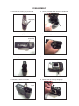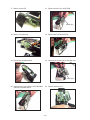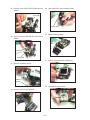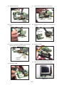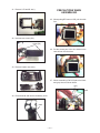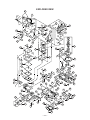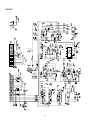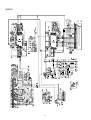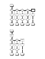
1
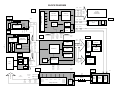
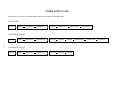
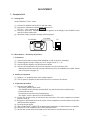
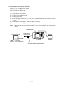
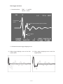
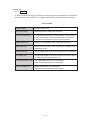
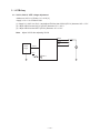
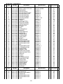
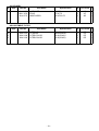
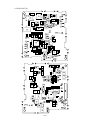
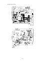
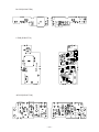
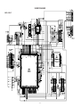
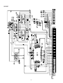
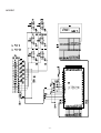
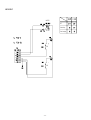
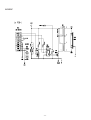
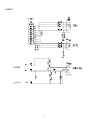
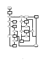
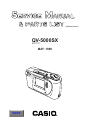
(without price)
QV-5000SX
(KX-777)
MAY. 1998
ZOO
M
MEN
DIS
U
P
MO
DE
POW
ER
FF
–
ON/O
+
REC
PLA
Y
LC
DO
N/O
FF
INDEX
R
CONTENTS
SPECIFICATIONS ....................................................................................................................................... 1
BLOCK DIAGRAM ...................................................................................................................................... 2
POWER SUPPLY FLOW ............................................................................................................................ 3
VOLTAGE TABLE ....................................................................................................................................... 4
ADJUSTMENT ............................................................................................................................................ 5
1. Complete Unit .................................................................................................................................... 5
1-1. Loading ADJ ................................................................................................................................. 5
1-2. White balance · Sensitivity adjustment ..................................................................................... 5
1-3. Flash operation and recharge operation ................................................................................... 7
1-4. Current consumption .................................................................................................................. 9
1-5. Operation check (Reference) ...................................................................................................... 9
1-6. Test mode ................................................................................................................................... 10
2. D-PCB Assy ...................................................................................................................................... 13
2-1. Operation check ......................................................................................................................... 13
3. L-PCB Assy ...................................................................................................................................... 15
3-1. VCC18, VCC15, VEE7 voltage adjustment ............................................................................... 15
DISASSEMBLY ......................................................................................................................................... 16
PRECAUTIONS WHEN ASSEMBLING .................................................................................................... 21
EXPLODED VIEW ..................................................................................................................................... 23
PARTS LIST .............................................................................................................................................. 24
PRINTED CIRCUIT BOARDS ................................................................................................................... 32
SCHEMATIC DIAGRAMS ......................................................................................................................... 37
TROUBLESHOOTING .............................................................................................................................. 45
SPECIFICATIONS
Item
Recording System
Recording Medium
Memory Capacity/
Computer Output image
Image Element
Computer Output image
Lens
Focusing
Aperture
Focus Range
Light Metering
Exposure Metering
Exposure Range
Exposure Correction
Shutter
Shutter Speed
White Balance
Self-timer
Recording Modes
Flash Modes
Monitor/Viewfinder
Video Output
Input/Output Terminals
Power Supply
Power Consumption
Dimensions
Weight
Standard Accessories
Specification
Digital (JPEG base); PC Link software can be used to input images in CAM, JPEG,
TIFF and other format.
Flash memory (8MB)
SUPER FINE: 16 images
(450KB compressed – 1280 x 960 pixels)
FINE: 30 images
(225KB compressed – 1280 x 960 pixels)
NORMAL: 57 images
(113KB compressed – 1280 x 960 pixels)
ECONOMY: 88 images
(64KB compressed – 640 x 480 pixels)
The above figures are approximations only. The actual number of images depends on
image subject matter.
1/3-inch CCD (Total Pixels: 1,310,000; Effective Pixels: 1,250,000)
1280 x 960 / 640 x 480 pixels
F2.8, f = 5.47mm
Selectable between phase-difference detection system autofocus and manual focus.
Lens shutter/auto iris
NORMAL: 0.3m to ∞
MACRO: 10cm
(From surface of protective lens.)
TTL center priority by CCD
Program AE
EV +6 to 17
–2EV to +2EV (1/2EV units)
CCD electronic shutter/mechanical shutter
1/8 to 1/500 second
Automatic
10 seconds
Single-image; Self-timer; Movie; Panorama; Title; Macro
AUTO, ON, OFF, Red-eye Reduction
1.8-inch TFT low-glare color LCD; 122,100 (555 x 220) pixels
NTSC/PAL (selectable)
DIGITAL OUT, VIDEO OUT, AC adaptor connector
Four batteries (AA-size alkaline or lithium batteries)/AC adaptor (AD-C620)
Approximately 7.6 W
131(W) x 69(H) x 43(D) mm
Approximately 250g (excluding batteries)
wrist strap; soft case; video cable; four LR6 alkaline batteries; owner’s manual
• The liquid crystal panel built into this camera is the product of precision engineering, with an effective pixel rate of
99.99%. This also means, however that 0.01% of the pixels can be expected to fail to light or to remain lit at all
times.
—1—
BLOCK DIAGRAM
26pin
L-PCB
VGH
VREFH
VGL
VREFL
GRES
GPCK
GSRT
12.75V
VCC13
7.5V
10pin
Comparator
sensor
Battery
Voltage
High voltage
generator
Xo
LAMP
SGND
PREN
VA
LTTRGN /SHUTTER
FBN
CM7018
TFT Controller
BL-PCB
VCC2
10pin
3.0V
VDD
VIDEO/RGB
SW
VIDEO75Ω
driver
6.0V
10pin
GND
VCC5-1
VCC1-ST
Serial
communication
buffer
B, G
R/VIDEO
AGND5
VCC5-1
CSYNC
VOUT
VCC1-L
LGND
BLCONT
PWCONT
DGND3
JKSW
SOP
SIP
DGND5
LGND
VIDEO
VGND
VSW
(B to B)
KA-PCB
20pin
16pin
KEY
(C FPC C)
NAND FLASH memory
64Mbit
—2—
SO
SCK
SUBCE
INHN
PACT
KIN0
KOUT0 KIN1
KOUT1 KIN2
VCC3-1 DGND3
FLASH/MASK memory
8Mbit
DCAM-101
Volrtage
detector
SUB
UNIT
COMMAND
STATUS
/SCK
/FLB
/SHUTTER
KIN0
KIN1
KIN2
/FLB
/LSRT
KIN3
KOUT2
DGND3
6pin
PW0~3
ADPTN
GND5
VCC5-1
SLED
DGND3
VCC3-1
60pin
(C FPC B)
PW-PCB
15pin
EVCC3
AGND3
VCC3-2
GND
VCC1-3
VCC1-L
CA481-TS
SUB-LCD
MODE
DISP
MENU
S/N/F/E
S-TIMER
FLASH
LC75821
LCD
Controller
KB-PCB
MSM82C55A
Extension I/O
EEPROM
CL-UNIT
(B to B)
DRAM ×2
32Mbit (50ns)
CPU
LCD
ON/OFF
F
Backlight controller
circuit
20pin
PLAY/REC
BLACTB
VCC3-1
SDIPO
SDOPO
AF-PCB
DRIVER
BLGND
DGND3
BLACTB
14pin
DB0
~
V3
DB9
V1
RSTCCD
CH3A
SHP
CH1A
SHD
V4
CLAMP
V2
SDI
CH3B
SCK
SUB
LOAD
CH1B
H1
OFDC
H2
RESET
/STBY1.2 RLED
GLED
V-Dr
Lens
BLCNT
HDB
BL-VCC
VEE2
XRD44L60
CDS/AGC/ADC
DRIVER
(B to B)
–14.5V
D-PCB
H-BUFFER
V-Dr
1.8"TFT
LCD Module
COD18T1022
51pin
2 color
LED
LZ23J3V
CCD
OE
CLR
HCNT BOUT
MCLK VDD
MODE1 VSH
VSS
GOUT
5.0V
BL-VCC
C-PCB
RESET
MODE2
CS
VCOM
VBC
SRTR
SRTL
VCC7
Voltage Controller
ST-UNIT
IR3Y26A1
RGB Interface
(C to F)
KEY
SHUTTER
(+)
(–)
20pin
(B to B)
AF-PCB
20pin
10pin
JK-IN
VCC1-ST
GND
16pin
VCC5-1
(C FPC C)
GND
AGND
5V
PGND
V. PM
VCC3-3
GND3
DGND
VCC
VCC18
VCC5-4
VCC15
GND4
3.3V
3.3V
18.5V
15V
–9V
5.0V
VCC3-1
VCC3-2
VCC3-3
EVCC3
VCC18
VCC15
VEE7
VCC5-1
VCC5-2
VCC5-3
VCC5-4
Voltage Controller
Battery
DC
JACK
VIDEO
JACK
Serial
Communication
Jack
Timer
LED
POWER SUPPLY FLOW
When power is turned on, the power supply flows in each mode are as shown below.
(1) PLAY MODE
PW2=H
PW2=L
(BLCONT=L
PWCONT=L)
PW2=H
(PWCONT=H
CSYNC Start
(BLCONT=L
PWCONT=L)
(PW1=H
PW3=H)
PW2=H
(BLCONT=L
PWCONT=L)
(PW1=H
PW3=H)
PW2=H
BLCONT=H)
(2) REC MODE, LCD ON
PW2=H
PW2=L
—3—
(3) REC MODE, LCD OFF
PW2=H
PW2=L
(PWCONT=H
CSYNC start
BLCONT=H)
VOLTAGE TABLE
PCB
Signal
VCC1-3
EVCC3
VCC3
D
C
—4—
AF
ST
L
VCC5-1
VCC18
VCC15
VCC5-4
VCC3
VEE7
VCC5-2
VCC5-3
VCC3-1
VCC1-ST
VCC5-1
F.B.
VCC3-1
VCC3-2
VCC3-4
VCC3-1
VCC3-3
VCC13
VCC7
VCC2
VEE2
VDD
VCC5-1
VCC3-1
BL-VCC
Voltage [V]
BATTERY
3.3
3.3
3.3
3.3
5.0
18.5
15.0
5.0
3.3
3.3
-9.0
5.0
5.0
3.3
BATTERY
5.0
13.5
7.5
5.0Adj
-15.0
3.0
5.0
3.3
6.0Adj
Control signal (“H” active)
Non, Sw,
Non, Sw,
PW0
PW0
PW0
PW2
PW1
PW1
PW3
PW0
PW0
PW3
PW1
PW1
PW0
Non, Sw,
PW2
PWCONT
PWCONT
PWCONT
PWCONT
PWCONT
PW2
PW0
PWCONT ∗ BLCONT
Main Bolock
F, F, (POWER SW)
CPU, Flash, ROM, RAM
CPU (Analog)
CCD, Strobe
Strobe (Logic)
VDr
CCD, VDr, Buff,
C-MOSBuff,
CDS, AGC, AD (Driver)
CDS, AGC, AD, VDr
CCD, VDr,
AFMotor
Eyeris, Measure
AF (Logic)
Strobe Charge
Strobe (Logic)
Disp (Gate)
Disp (Source) RGB I/F
RGBI/F
Disp (Gate)
Disp (Logic), TFTController
Video Out, Serial
SignalSW, Serial
BackLight
ADJUSTMENT
1. Complete Unit
1-1. Loading ADJ
Set QV-5000SX to “PLAY” mode.
[
[
(1) Connect QV-5000SX and DOS/V PC with link cable.
(2) Execute the adjustment software shown below on PC.
DT777E - aok 98042101.adj ENTER
(3) During the procedure, “MEMORY ERROR#4” appears on the display of QV-5000SX but this
does not indicate malfunction.
(4) Parameter loading complete message will be displayed.
QV-5000SX
Link cable
PC
RS232C port
1-2. White balance · Sensitivity adjustment
1. Preparation
(1)
(2)
(3)
(4)
Viewer (Kenko light box handy 5000) (Modified in order to input DC externally)
Voltage regulator (Output voltage: 0 to 10 V, Output current: 0 ~ 1 A)
Use two ND filter together, one ND10 and one ND20.
Use two color temperature converter filter together, one LA10 and one LA20.
* Although those filters are sold at a large camera store, they are available from CASIO. Please
refer to the parts list (page 31).
2. Setting of equipment
(1) Supply 6 V to simplified viewer from voltage regulator.
(2) Turn on power of simplified viewer and leave it on for more than 30 minutes.
3. Adjustment procedure
(1) Start test mode MENU2.
• Set function switch to REC mode
• Turn POWER switch ON while pressing DISP key and Shutter button simultaneously.
• Press mode key twice
• Press flash key and menu key simultaneously.
(On display, cursor is placed on CCD RGB ADJUST)
(2) Set the filter so that center of illuminance face and center of two color temperature converter
filters are lined up.
(3) Bring lens of QV-5000SX close to the center of color temperature converter filters then stick QV5000SX and filters together.
(4) Press the shutter button.
(5) When RGB ADJUST COMPLETE is displayed the initialization, of white balance is completed.
(6) Remove two color temperature filters from simplified viewer.
(7) Set the filter so that center of illuminance face and center of two ND filters are lined up.
—5—
(8) Bring lens of QV-5000SX close to the center of ND filters, then stick QV-5000SX and filters
together.
(9) Press the shutter button.
(10) When SENS ADJ COMPLETE is displayed the adjustment of sensitivity is completed.
(11) Turn power switch off.
• When using kenko light box handy 5000 go on with the procedure listed below, 12. to 15.
Execute them only once. If you execute more than once start from procedure 1.
(12) Set function switch to PLAY mode, then turn on power.
(13) Connect QV-5000SX and PC with a link cable then execute R, BGAIN compensation software
(kadj1E.exe) on Windows 95.
(14) Click “replace AD”.
(15) White balance adjustment is completed when “AD replacement complete” is displayed.
4. Checking Adjustment
(1) White balance
• Set white balance manually to sunlight.
• Turn on the power switch of simplified viewer and take a picture.
• Compare it with a regular picture and if there are no difference, its setting is OK.
(2) Sensitivity
• Set strobe to AUTO.
• Take a picture of a person’s face in a dark room at a distance of about 1 meter.
• Compare it with a regular picture and if there are no difference, its setting is OK.
PRECAUTIONS
• Since the intensity of light and color temperature varies in the simplified viewer, let it sit for 30
minutes before using.
• The deviation of simplified viewer’s illuminace face’s point light intensity is large, try to set the
illuminace face at the center.
• Pay attention since the figure of R, BGAIN compensation software (kadj1E. exe) keeps changing.
Equipment needed to execute white balance and sensitivity adjustment
Light source (viewer)
ADJ SOFT
Color temperature
(K) light source 1
No. 1
CCD RGB ADJUST
4400 ± 200
No. 2
CCD SENS ADJUST
Light intensisty
(cd/m2) light source 2
Note
No specified figure for
light intensity
50 ± 5
—6—
No specified figure for
color temperature
1-3. Flash operation and recharge operation
• Apply 6.0 ± 0.1 V voltage on DC in jack.
• Set QV-5000SX in “REC” mode.
• Perform after flash adjustment.
(1)
(2)
(3)
(4)
(5)
Shoot a picture with flash ON.
Shoot in red eye reduction mode.
Shoot in macro mode.
Set QV-5000SX in “PLAY” mode and check the pictures taken.
Monitor the trigger waveform of (1), (2) and (3) on a digital oscilloscope and make sure there are
no errors.
(6) Shoot a picture with flash OFF. (Make sure there is no flash)
(7) Make sure that the charging current is less than 1.3 A.
Note:
Make sure that the pictures taken in steps (1) and (2) are not whitish, dark or erroneously
colored.
Flash lens face
Digital oscilloscope
TIME : 1.0 µsec/DIV
VOLTS: 1 V/DIV (AC mode)
Probe close to
flash lens face
Monitor
QV-5000SX
Earth of hte probe
Should be hooked as shown above.
—7—
Flash trigger waveform
1. Normal waveform
CH1
TIME : 1 µ sec/DIV
VOLTS : 1 V/DIV
1V
1µV
757µV
UERT
First positive
pulse.
OK if second positive pulse is shown.
First negative
pulse.
ACQUIRE
NORMAL
2
AVS
1
ENVELOPE
REPET SAVE ON
ON | OFF ON | OFF
2. NG waveforms when trigger skipping occurs.
(1) When trigger skipping occurs on the first
positive pulse.
(2) When trigger skipping occurs on the first
negative pulse.
—8—
1-4. Current consumption
Set QV-5000SX to “PLAY” mode.
(1) Current consumption (DC in = 6.0 ± 0.1 [V])
(2) Lower the voltage from 6 V as shown below then make sure the battery warning indicator changes.
DC in = 5.0 ± 0.05 [V] (PLAY mode)
DC in = 4.65 ± 0.05 [V] (PLAY mode)
Note:
Make sure that current consumption is less than 550 mA in PLAY mode.
Reference: • Current consumption of REC mode.
• Maximum 800 mA (Flash charge current is not included)
1-5. Operation check (Reference)
(1)
(2)
(3)
(4)
(5)
(6)
(7)
(8)
(9)
Shock resistance, battery operation
Jack operation, slide switch operation, button operation.
Cover open/close operation, battery cover open/close operation
Resolution, paralax, color revival
Standard/Macro switch, AE operation, AF operation, self timer countdown display
Flash display function, LED display function
Video output, digital communication, page display
Dust and scratches on lens
Appearance
Notes: • In MACRO mode make sure the focus gets clear at a distance of 100 ± 4 mm from the front
part of protector.
• In NORMAL mode make sure you are able to see the specified resolution specified on the
center resolution chart and 79 % chart at a distance of 300 ± 10 mm.
• Operate the procedures listed below as a secondary judgement of procedure (2).
• In NORMAL mode make sure you are able to see the specified resolution specified on the
center resolution chart and 85 % chart at a distance of 1000 ± 10 mm.
* Take a shot at F mode then check the resolution after loading it to the PC.
* After checking on the PC. Adjustments are made only when there is a problem.
• Plates, letters, screws, label are to be checked as appearance.
• Check the color revival using tint chart and the noise level
Make sure the figures on video outputs are as shown below.
~ROM98022502: 1.0 V ± 0.2V (test pattern white100 %)
ROM98022601~: 0.82V ± 0.2V (test pattern white 75 %)
* Operate at 75 Ω end terminal.
• Make sure the setting “NTSC/PAL” after D-PCB replacement.
—9—
1-6. Test mode
(1) Turn power ON while pressing shutter button and DISP button simultaneously.
TEST MODE display is displayed.
TEST MODE
PATCH
11111111
LOADER
7
ADj.
98012201
VER.
98012201
In the center of the display “TEST MODE” is displayed at 4 times the size of other letters.
In the lower right corner PATCH, LOADER, ADj and Program version are displayed.
PATCH : When there is no PATCH, 11111111 will be displayed
ADJ
: When ADJ is broken or CCD is not adjusted, dates will not be displayed.
(2) Press MENU button and FLASH button simultaneously.
MENU 1 appears on the display.
(3) Double click MODE key then press MENU button and FLASH button simultaneously.
MENU 2 appears on the display
• Press +/– to select and SHUTTER button to confirm.
— 10 —
MENU1
1.
2.
3.
4.
5.
6.
7.
8.
INIT. SETTING NTSC
INIT. SETTING PAL
GRAY SCALE (10STEP)
BLACK
50% GRAY
WHITE
CROSS HATCH
COLOR BAR
MENU1-1
MENU1-2
Set at factory.
1. RECLCD: ON
2. ON
3. FLASH: AUTO
4. QUALITY: F
5. WB: AUTO
6. PICTURE: NORMAL
7. MOVIE TIME: 3.2 sec
8. TITLE
9. Zoom:
10. VIDEO OUT: NTSC or PAL
MENU1-3
Displays 10 steps of grey scale.
Light intensity values are 16, 38 ,60, 82, 104, 126, 148, 170, 192, 214, 235
MENU1-4
Black display
MENU1-5
50 % gray display
MENU1-6
White display
MENU1-7
32 × 32 pixel grid pattern on black, or RED square at REC Thru (320 × 216) or
Yellow square at PLAY MODE (360 × 240) or 1 PIXEL mark is displayed in the
center.
MENU1-8
Displays color bar.
— 11 —
MENU2
1.
2.
3.
4.
5.
6.
7.
8.
9.
CCD RGB ADJUST
CCD SENS. ADJUST
BATT. TEST
REC INFO.
SELF COPY
IMAGE COPY
MOTOR SETTING
SOKKYO CHANGE
NO COMP CAPT
MENU2-1
Execute CCD color solid adjustment, then record it on ADJ of flash memory
display.
Press shutter button by adjusting the light amount using specified filters in
specified viewer.
When setting mark is displayed it is completed.
MENU2-2
Execute CCD sensitivity check, check result is stored in ADJ area of the picture
flash memory.
Press shutter button by adjusting the light amount using specified filter in
specified viewer.
When setting mark is displayed, it is completed.
MENU2-3
Battery life measurement function.
When shutter button is pressed, it will shoot pictures at interval of about 10
seconds. It will go off when battery goes dead or when power is turned off.
MENU2-4
FOCUS/iris display function
At REC through, present Focus point and iris will be displayed on the LCD.
It will be easy to control Manual Focus precisely.
It will go off when power is turned off.
Do not use 5 to 9 of MENU2 because it will corrupt data stored.
— 12 —
2. D-PCB Assy
2-1. Operation check
• Set QV-5000SX in “PLAY” mode.
• Connect C, L, PW, KA, KB, JK, BL PCB.
• Connect PACT (CP510) to GND for short time (1, 2 seconds).
Then the unit will be operation mode.
Supply electricity to each power source of D PCB.
VCC3-1; 3.3 ± 0.08V
EVCC; 3.3 ± 0.08V
VCC5-1; 5.0 ± 0.1V
VCC1-3; 6.0 ± 0.08V
AC adaptor can be used. But if the unit does not operate correctly use the values listed above.
1. Clock frequency check
Make sure SYSCLKP terminal is at f0 = 54MHz ± 60ppm.
2. DT program check
Program used: dt777E
Check the items listed below.
(1) Make sure serial communication connection is OK.
(2) Check ROM version.
(3) Make sure DRAM is OK.
(4) Make sure flash memory is OK.
(5) Check the voltages detected. (HIGH will be displayed)
(vcc1-3 voltage high; 6.0 ± 0.1 V, middle; 4.5 ± 0.1 V, low; 4.0 ± 0.1 V)
(6) Check that each mode is OK.
• REC/PLAY mode
• VIDEO jack used/not used
• AC adaptor jack used/not used
(7) Make sure each key works correctly.
(8) Make sure each LED lights.
• LED for self timer
• Operation display LED
(9) Make sure TFT LCD display goes on an off correctly.
(10) Make sure SUB LCD lights.
(11) Turn power OFF.
3. Make sure RGB and VIDEO are outputted.
For VIDEO, check each of NTSC type and PAL type.
Note:
Make sure video signal level are as shown below.
ROM version (~98022502) : 0.810 V ± 0.160 (100 % white)
ROM version (98022601~) : 0.665 V ± 0.150 ( 75 % white)
— 13 —
How to use
dt777E ENTER
To check D PCB (dt777E.exe), you will have to enter into serial communication for D PCB alone.
For host computer use 1 MB PC-AT compatible. Add check circuit to connectors as needed.
TEST contents
Version display
Displays ROM version.
Self test of DRAM
Read/write check of video buffer area only.
Check of control block
If no errors are found “OK” will be displayed. If any errors are
found FLASH memory will be formatted. (about 30 seconds)
In this case, all the pictures in memory will be deleted.
Voltage detect test
Displays the voltage detected by HIGH, MID, and LOW.
Mode detect test
Detect REC/PLAY mode, video out mode, AC adapter mode,
and displays result.
Detects each key
Test by pressing keys. Press the key that is shown on the display.
LED display test
Test operation display of self timer, follow the procedures shown
on display, and check if the lights go on.
LCD display ON/OFF test
Turn LCD display OFF then turn it ON again
Follow the procedures shown on the display.
Sub LCD display test
Display all segments, then erase them.
Follow the procedures shown on the display.
— 14 —
3. L-PCB Assy
3-1. VCC18, VCC15, VEE7 voltage adjustment
• Make sure VCC1-1 (CP149) = 5.0 ± 0.05 [V]
• Apply 3.3 V ± 5 % to PW0 to PW3.
(1) Apply 5.0 ± 0.05 V to VCC1-1 and adjust VR120 so that VCC18 (CP121) becomes 18.5 ± 0.5 V.
(2) Adjust VR125 so that VCC15 (CP125) becomes 15.0 ± 0.2 V.
(3) Adjust VR130 so that VEE7 (CP133) becomes –9.0 ± 0.2 V.
Note:
Adjust VCC15 after adjusting VCC18.
VCC18
L-PCB
VCC15
VEE7
Power
Supply
VCC1-L
V
3.3 V
PW~3
— 15 —
DISASSEMBLY
1. Unscrew two screws (S4) on the side.
5. Use a (–) screwdriver to remove the small hook.
screw (S4)
hook
2. Unscrew a screw (S4) on the bottom.
6. Remove the upper case.
screw (S4)
3. Open battery cover.
7. It should look like this.
4. Release the hook on the side.
8. Remove the top case by lifting it up.
hook
— 16 —
9. It should look like this.
13. Remove the label that says “CAUTION HIGH
VOLTAGE”
10. Remove the hook of battery holder.
14. Connect resistor (1.5 k Ω 5W) to flash
capacitor for discharging.
hook
11. Pull out the frame block.
15. Put purple wire on top then green, yellow and
gray on the bottom when assembling the top
part of the lens.
purple
yellow
green
gray
12. Frame block
16. Peel off the insulation sheet on the bottom.
insulation
sheet
— 17 —
17. Bottom view (LCD)
21. Remove a screw (S1) of KB PCB.
screw (S1)
18. Bottom view (camera)
22. Remove KA PCB and KB PCB.
19. Peel off the insulation sheet.
23. Unscrew two screws (S1) of the flash unit.
screw (S1)
20. Unscrew two screws (S9) of KA PCB hidden
under the insulation sheet.
24. Remove the flash unit.
— 18 —
25. Unscrew screw (S8) of PW PCB and remove
washer.
29. Unscrew a screw (S5) of battery holder.
scew (S8)
screw (S5)
30. Remove battery holder.
26. Unscrew screws (S8) and (S1) and remove
washer.
screw (S1)
screw (S8)
31. Peel off insulation sheet of lens ass’y.
27. Remove the battery spring.
battery
spring
32. Unscrew two (S2) screws.
28. Remove PW PCB and JK PCB.
— 19 —
33. Remove flash unit.
37. Unscrew two screws (S1) of lens ass’y.
screw (S1)
34. Unscrew a screw (S2) from metallic part on D
PCB.
38. Remove lens ass’y. Remove a screw (S2) of
L PCB.
screw (S2)
35. Remove connector (CN540). When assembling be sure the contact is secure.
39. Remove L PCB.
connector
(CN540)
40. Unscrew two screws (S1) of DP frame.
36. Remove D PCB.
screw (S1)
— 20 —
41. Remove LCD and BL ass’y.
PRECAUTIONS WHEN
ASSEMBLING
45. When putting DP frame to LCD, pull the cable
first.
42. Unscrew two screws (S4).
screw (S4)
46. Put the excess part of the wire inside so the
case will not nich the wires.
43. Remove bottom case ass’y.
47. When assembling PW PCB place the black
and gray wires as shown below.
gray
black
44. Press the shaft and remove the battery cover.
shaft
— 21 —
48. Let the black wire and gray wire run as shown.
gray
black
49. Wiring under KB PCB.
50. Wiring of upper lens ass’y.
— 22 —
EXPLODED VIEW
S1
1
57
10
S8
8
S1
S2 4
62
63
S1
S2
S2
6
55
S8
56
S2
58
13
S7
S7
30
7
31
S2
9
11
3
26
61
29
60
25
27
54
59
20
21
28
2
22
32
S9
5
S7
42
S4
14
16
S4
S6
32
33
48
45
47
S1
24
15
S9
S5
S3
40
41
35
E1
36
12
52
S4
34
17
49
23
51
53 46
43
19
— 23 —
39
50
44
18
37
38
PART PRICE LIST
DIGITAL PCB ASSY
N
N
N
N
N
N
N
N
N
N
N
N
N
N
N
N
N
N
N
N
N
N
N
N
N
Item
Part No.
Part Name
Specification
Ics
2105 6486 IC
2105 5215 IC
2114 4676 IC
2105 6472 IC
2105 6244 IC
2105 6471 IC
2105 6488 IC
2105 6491 IC
2105 6493 IC
2105 6470 IC
2105 6492 IC
2105 6473 IC
2105 6473 IC
2105 5719 IC
2765 2183 LSI
2012 6033 LSI
2012 6033 LSI
CONNECTOR
CN578 3502 2441 CONNECTOR
CN580 3502 2441 CONNECTOR
TRANSISTORS
Q400
2250 1162 TRANSISTOR/CHIP
Q405
2259 2715 TRANSISTOR/DIGITAL
Q440
2259 2745 TRANSISTOR/DIGITAL
Q441
2259 2745 TRANSISTOR/DIGITAL
Q442
2259 2745 TRANSISTOR/DIGITAL
Q443
2259 2745 TRANSISTOR/DIGITAL
Q444
2795 8150 FET/CHIP
OSCILLATORS
H450
2590 2722 OSCILLATOR
H452
2590 2745 OSCILLATOR
H454
2590 2744 OSCILLATOR
IC400
IC410
IC412
IC414
IC415
IC420
IC426
IC427
IC428
IC458
IC460
IC500
IC502
IC505
IC510
IC560
IC561
- 24 -
Q Price Code R
MB81V18165B50LPFTN
MB81V18165B50LPFTN
1
1
1
1
1
1
1
1
1
1
1
1
1
1
1
1
1
AC
AE
AD
AF
AC
BC
AC
AC
AC
AL
AC
AF
AF
AE
CY
BT
BT
C
C
C
C
C
C
C
C
C
C
C
C
C
C
C
C
C
54154-0209
54154-0209
1
1
AD
AD
X
X
2SA1576A-T106R
DTC144EE-TL
DTC143EE-TL
DTC143EE-TL
DTC143EE-TL
DTC143EE-TL
2SK2035(TE85L)
1
1
1
1
1
1
1
AA
AA
AA
AA
AA
AA
AA
B
B
B
B
B
B
B
SPT2A-32KHz
CX-51F-27.0M
CX-51F-20.0M
1
1
1
AG
AP
AP
C
C
C
S-80835ANNP-EDZ-T2
TC7W74FU(TE12L)
TC7W04FU(TE12L)
TC74AC00FT(EL)
TC7S32FU(TE85L)
MSM82C55A-2GS-2K
S-80847ANNP-EJB-T2
S-80842ANNP-ED6-T2
PST9337UR
LM4041CIM3X-1.2
PST9330UR
TC7WH125FU(TE12L)
TC7WH125FU(TE12L)
TC7W32FU(TE12L)
KM29V64000T
LINER PCB ASSY
N
N
N
N
N
N
N
N
Item
IC150
IC180
IC300
IC302
IC310
IC315
IC340
IC390
IC900
CN320
CN901
CN300
SW300
N
N
Q152
Q155
Q300
Q301
Q310
Q900
D160
D161
D162
D163
D190
D300
D310
D757
D778
N
N
FU101
FU900
VR151
VR320
VR340
VR344
VR381
VR755
VR900
T155
Part No.
Part Name
Specification
Ics
2114 5800 IC
2105 4501 IC
2254 0550 IC
2254 0550 IC
2105 6490 IC
2105 5712 IC
2114 5846 IC
2114 5805 IC
2114 5842 IC
CONNECTORS
3502 2436 CONNECTOR
3502 2436 CONNECTOR
3502 2442 CONNECTOR
SWITCH
3412 1106 SWITCH/SLIDE
TRANSISTORS
2259 2715 TRANSISTOR/DIGITAL
2259 2757 TRANSISTOR/CHIP
2259 2715 TRANSISTOR/DIGITAL
2259 2715 TRANSISTOR/DIGITAL
2254 0448 FET/CHIP
2259 2757 TRANSISTOR/CHIP
DIODES
2390 1820 DIODE/CHIP
2390 1820 DIODE/CHIP
2390 1379 DIODE/SCHOTTKY/CHIP
2390 1820 DIODE/CHIP
2390 1379 DIODE/SCHOTTKY/CHIP
2390 1379 DIODE/SCHOTTKY/CHIP
2390 1379 DIODE/SCHOTTKY/CHIP
2390 1358 DIODE/VARICAP
2390 1820 DIODE/CHIP
FUSES
2797 4977 JUMPER/CHIP
2797 5589 FUSE
VARIABLE RESISTORS
2775 1470 RESISTOR/SEMIFIXED/CHIP
2775 1827 RESISTOR/SEMIFIXED/CHIP
2775 1491 RESISTOR/SEMIFIXED/CHIP
2775 1491 RESISTOR/SEMIFIXED/CHIP
2775 1484 RESISTOR/SEMIFIXED/CHIP
2775 1484 RESISTOR/SEMIFIXED/CHIP
2775 1505 RESISTOR/SEMIFIXED/CHIP
CONVERTER
3065 0713 CONVERTER/DC-DC
- 25 -
Q Price Code R
MB3800PFV-G-BND-EF
RN5RL30AA-TR
TC7W66FU(TE12L)
TC7W66FU(TE12L)
TK15405MTL
TC7S04FU(TE85L)
IR3Y26A1
NJM3414AV-TE1
S-8327E50MC-EKE-T2
1
1
1
1
1
1
1
1
1
AP
AD
AD
AD
AH
AD
BH
AI
AI
C
C
C
C
C
C
C
C
C
52465-1091
52465-1091
53887-0209
1
1
1
AD
AD
AF
X
X
X
SSSS212-12-B
1
AC
C
DTC144EE-TL
2SD2150-T100R
DTC144EE-TL
DTC144EE-TL
2SK1580-T1
2SD2150-T100R
1
1
1
1
1
1
AA
AB
AA
AA
AC
AB
B
B
B
B
B
B
1SS355-TE-17
1SS355-TE-17
MA729-(TX)
1SS355-TE-17
MA729-(TX)
MA729-(TX)
MA729-(TX)
MA329-(TX)
1SS355-TE-17
1
1
1
1
1
1
1
1
1
AA
AA
AB
AA
AB
AB
AB
AC
AA
X
X
X
X
X
X
X
X
X
ERJ2GE0R00X
PI-R429.375
1
1
AA
AC
B
B
EVM-1XSX50B53
EVM-1XSX50B13
EVM-1XSX50B54
EVM-1XSX50B54
EVM-1XSX50B24
EVM-1XSX50B24
EVM-1XSX50B55
1
1
1
1
1
1
1
AB
AB
AB
AB
AB
AB
AB
C
C
C
C
C
C
C
6CA-02
1
AM
C
POWER PCB ASSY
N
N
N
Item
N
N
N
N
IC110
IC115
IC120
IC125
IC127
IC130
IC135
IC137
IC139
IC140
N
N
CN112
CN114
N
N
N
N
N
N
N
N
Q110
Q111
Q120
Q121
Q122
Q126
Q127
Q130
Q131
Q140
Q195
D100
D110
D120
D127
D130
D131
D140
D195
FU102
FU103
FU104
VR130
VR120
VR125
Part No.
Part Name
Specification
Ics
2105 6480 IC
2105 6479 IC
2114 5842 IC
2105 6477 IC
2105 6478 IC
2114 5607 IC
2114 5849 IC
2114 5849 IC
2114 5849 IC
2105 6480 IC
CONNECTORS
3502 2443 CONNECTOR
3502 2442 CONNECTOR
TRANSISTORS
2114 5807 FET/CHIP
2259 2745 TRANSISTOR/DIGITAL
2251 0847 TRANSISTOR/CHIP
2259 2715 TRANSISTOR/DIGITAL
2259 2757 TRANSISTOR/CHIP
2259 2715 TRANSISTOR/DIGITAL
2105 6481 FET/CHIP
2259 2715 TRANSISTOR/DIGITAL
2250 1579 TRANSISTOR/CHIP
2114 5807 FET/CHIP
2259 2715 TRANSISTOR/DIGITAL
DIODES
2390 2506 DIODE/CHIP
2390 1883 DIODE/CHIP
2390 1883 DIODE/SCHOTTKY/CHIP
2390 1883 DIODE/SCHOTTKY/CHIP
2390 1379 DIODE/SCHOTTKY/CHIP
2390 1820 DIODE/CHIP
2390 1883 DIODE/SCHOTTKY/CHIP
3013 2611 LED/CHIP
FUSES
2797 5592 FUSE
2797 5593 FUSE
2797 5593 FUSE
VARIABLE RESISTOR
2775 1484 RESISTOR/SEMIFIXED/CHIP
2775 1491 RESISTOR/SEMIFIXED/CHIP
2775 1491 RESISTOR/SEMIFIXED/CHIP
- 26 -
Q Price Code R
S-8520B33MC-ARS-T2
RN5RL33AA-TR
S-8327E50MC-EKE-T2
LP2951CMX
RH5RH553B-T1
TK11830MTL
TK11250BMCL
TK11250BMCL
TK11250BMCL
S-8520B33MC-ARS-T2
1
1
1
1
1
1
1
1
1
1
AL
AC
AI
AM
AK
AL
AE
AE
AE
AL
C
C
C
C
C
C
C
C
C
C
52746-1690
53887-0209
1
1
AC
AF
C
C
SI3441DV-T1
DTC143EE-TL
2SB1386-T100R
DTC144EE-TL
2SD2150-T100R
DTC144EE-TL
SI3442DV-T1
DTC144EE-TL
2SA1774-TLR
SI3441DV-T1
DTC144EE-TL
1
1
1
1
1
1
1
1
1
1
1
AK
AA
AD
AA
AB
AA
AH
AA
AA
AK
AA
B
B
B
B
B
B
B
B
B
B
B
RB060L-40TE25
RB160L-40TE-25
RB160L-40TE-25
RB160L-40TE-25
MA729-(TX)
1SS355-TE-17
RB160L-40TE-25
SML-010JTT86
1
1
1
1
1
1
1
1
AD
AC
AC
AC
AB
AA
AC
AB
C
C
C
C
C
C
C
C
TR1608FF-1A
TR1608FF-1.5A
TR1608FF-1.5A
1
1
1
AC
AC
AC
B
B
B
EVM-1XSX50B24
EVM-1XSX50B54
EVM-1XSX50B54
1
1
1
AB
AB
AB
C
C
C
JACK PCB ASSY
N
N
N
Item
Part No.
Part Name
Specification
CONNECTOR
CN101 3502 2445 CONNECTOR
FUSE
FU100 2797 5594 FUSE
JACKS
JK100
3501 6755 JACK/POWER
JK101
3501 8197 JACK/MINI
JK102
3502 2439 JACK
Q Price Code R
53309-1090
1
AC
C
PI-R429002
1
AC
B
HEC3600-010120
HSJ1169-019010
HSJ1456-01-220
1
1
1
AD
AF
AC
C
C
C
KEYBOARD(A) PCB ASSY
N
Item
N
IC800
N
SW830
SW800
SW801
SW802
SW804
SW805
SW806
D800
D801
D802
D804
D805
D806
Part No.
IC
2114 5847
SWITCHES
3412 2083
3412 2068
3412 2068
3412 2068
3412 2068
3412 2068
3412 2068
DIODES
2390 1820
2390 1820
2390 1820
2390 1820
2390 1820
2390 1820
Part Name
Specification
Q Price Code R
IC
LC75821W
1
AT
C
SWITCH
SWITCH
SWITCH
SWITCH
SWITCH
SWITCH
SWITCH
MSS-26
EVQPQHB55
EVQPQHB55
EVQPQHB55
EVQPQHB55
EVQPQHB55
EVQPQHB55
1
1
1
1
1
1
1
AD
AB
AB
AB
AB
AB
AB
C
C
C
C
C
C
C
DIODE/CHIP
DIODE/CHIP
DIODE/CHIP
DIODE/CHIP
DIODE/CHIP
DIODE/CHIP
1SS355-TE-17
1SS355-TE-17
1SS355-TE-17
1SS355-TE-17
1SS355-TE-17
1SS355-TE-17
1
1
1
1
1
1
AA
AA
AA
AA
AA
AA
C
C
C
C
C
C
- 27 -
KEYBOARD(B) PCB ASSY
N
Item
CN810
N
N
N
SW810
SW811
SW820
D808
D809
D810
D811
Part No.
Part Name
Specification
CONNECTOR
3502 2412 CONNECTOR
SWITCHES
3412 1519 SWITCH/TACT
3412 1519 SWITCH/TACT
3412 2085 SWITCH/TACT
DIODES
2390 1820 DIODE/CHIP
2390 1820 DIODE/CHIP
2390 1820 DIODE/CHIP
2390 1820 DIODE/CHIP
Q Price Code R
52745-0690
1
AB
C
SKQMAH-T3
SKQMAH-T3
SKQAAA-T
1
1
1
AC
AC
AC
C
C
C
1SS355-TE-17
1SS355-TE-17
1SS355-TE-17
1SS355-TE-17
1
1
1
1
AA
AA
AA
AA
C
C
C
C
BACK LIGHT PCB ASSY
N
Item
Part No.
Part Name
Specification
IC
2105 6463 IC
CONNECTOR
CN900 3502 2444 CONNECTOR
SWITCH
SW900 3412 2068 SWITCH
TRANSISTORS
Q920
2259 2715 TRANSISTOR/DIGITAL
Q924
2253 0700 FET/CHIP
TRANSFORMER
T920
3012 1414 TRANSFORMER/INVERTER
IC920
N
- 28 -
Q Price Code R
TC7ST02FU(TE85L)
1
AD
C
53353-1091
1
AE
C
EVQPQHB55
1
AB
C
DTC144EE-TL
2SK1485-T1
1
1
AA
AG
B
B
BLC10-01
1
AM
C
MAIN BODY COMPONENT
N
Item
Part No.
N
N
N
N
N
N
N
N
N
N
N
N
N
N
N
N
N
N
N
N
N
N
N
N
N
N
N
N
N
N
N
N
N
N
N
N
N
N
N
N
N
N
N
N
N
N
1
2
3
4
5
6
7
8
9
10
11
12
13
14
15
16
17
18
19
20
21
22
23
24
25
26
27
28
29
30
31
32
33
34
35
36
37
38
39
40
41
42
43
44
45
46
47
1014 9879
2725 1347
6613 0620
6613 0830
6613 0831
6613 0832
6613 0840
6613 0842
6613 0843
6613 0844
6613 0846
6613 0875
6613 0876
6613 0877
6613 0880
6613 0890
6613 0900
6613 0910
6613 0920
6613 0930
6613 0940
6613 2240
6613 0960
6613 1080
6613 1090
6613 1100
6613 1110
6613 1120
6613 1130
6613 1140
6613 2791
6613 3500
6613 3510
6613 1200
6613 1210
6613 1220
6613 1230
6613 1240
6613 1250
6613 1260
6613 1270
6613 1280
6613 1290
6613 1300
6613 1310
6613 1320
6613 1330
N
Item
Part No.
N
N
N
N
N
N
N
48
49
50
51
52
53
54
6613 1340
6613 1360
6613 1370
6613 1380
6613 1390
6613 1400
6613 1430
Part Name
Specification
STROBE UNIT
DISPLAY ASSY/TFT LCD
PANEL/REAR
PCB ASSY/JACK
PCB ASSY/BACK LIGHT
PCB ASSY/SHUTTER
PCB ASSY/DIGITAL
PCB ASSY/POWER
PCB ASSY/LINEAR
LENS ASSY
BL ASSY
COVER/BATTERY
LENS ASSY/PANEL
COVER/CONSOLE
PCB ASSY/TOP
BUTTON
SHAFT
PLATE/DISPLAY
KNOB/REC
COVER/SENSOR
COVER/LED
COVER/FINDER
PLATE/RATING
CASE/LOWER
MAGNET
COVER/STROBE
TAPE/DOUBLE SIDE
TAPE/DOUBLE SIDE
TAPE/DOUBLE SIDE
GRIP
TAPE/DOUBLE SIDE
PLATE/INSULATION
SPACER/TAPE
CASE/BOTTOM
SCREW/FOR STAND
LABEL/FOR BATTERY
CASE/TOP
BUTTON
BUTTON
BUTTON/SHUTTER
SPRING/SHUTTER
CASE/UPPER
COVER/DISPLAY
COVER/FINDER
CASE/FINDER
KNOB/POWER
PIN/STRAP
Part Name
CO-777
COD18T1022RN
K140444-1
K341261*1
K341261*2
K341261*3
K140476*1
K240967*1
K140477*1 M
K341231*1
K441390*1
K341277*1
K240983*1
K441444*1
K341281*1
K341041-1
K441310-1
K441302-1
K341039-1
K341055-1
K341036-1
K441471-1
K441441-1
K140447-1
K441281-1
K341064-1
K441445-2
K441445-3
K441314-1
K140487-1
K441501A-1
K441494-8
K441522-1
K140449-1
K341059-1
K441442-1
K140446-1
K341042-1
K240866-1
K341044-1
K441297-1
K140451-1
K140450-1
K140445-1
K240857-1
K341037-1
R340181-2
Specification
SPRING/POWER
BUTTON/LCD
PROTECTOR/FINDER
COVER/LED
TAPE/DOUBLE SIDE
TAPE/DOUBLE SIDE
CABLE
- 29 -
K441298-1
K341038-1
K441299-1
K341054-1
K441445-4
K441445-5
K341005-1
Q Price Code R
1
1
1
1
1
1
1
1
1
1
1
1
1
1
1
1
1
1
1
1
1
1
1
1
1
1
1
2
1
1
1
5
1
1
1
1
1
1
1
1
1
1
1
1
1
1
1
CN
DI
BT
CN
CL
CG
EH
DG
DI
EJ
CQ
AZ
CI
AV
BX
AI
AA
AD
AB
AB
AB
AN
AA
AP
AF
AE
AA
AA
AA
AD
AA
AA
AA
AL
AC
AA
AL
AI
AK
AH
AA
AR
AL
AD
AA
AA
AE
A
A
X
A
A
A
A
A
A
A
A
B
C
X
A
C
X
X
C
X
X
X
X
C
X
X
X
X
X
X
X
X
X
X
X
X
C
C
C
C
C
C
X
X
X
C
C
Q Price Code R
1
1
1
1
3
2
1
AA
AB
AC
AA
AA
AA
AE
C
C
X
X
X
X
X
N
N
N
N
N
N
N
N
N
N
N
N
N
N
55
56
57
58
59
60
61
62
63
E1
S1
S2
S3
S4
S5
S6
S7
S8
S9
6613 1450
6614 0750
6613 1470
6613 1480
6613 1510
6613 1520
6613 1530
6614 0760
6614 0770
5861 3649
5112 0868
5860 0301
5860 2380
5860 3381
5861 3527
5861 3698
5861 3742
5861 3741
6330 5240
1915 3723
HOLDER/BATTERY
SPRING/BATTERY
CABLE
CABLE
SPACER/SHEET
SHEET/FILTER
SHEET/DIFFUSION
SPRING/BATTERY
SPRING/BATTERY
E RING
SCREW
SCREW
SCREW
SCREW
SCREW
SCREW
SCREW
SCREW
SCREW
IGBT
K240858-1
K441296-1
K240915-1
K140422-1
K441309-1
K441308-1
K441307-1
K441295-1
K441294-1
1.5 JISB2805
BT3 1.7X5 BK
BT3 1.7X3.5 NI
PS3 1.7X3.5 BK
PS3 1.7X4 BK
BT3 1.7X2.5 BK
PS1 1.7XZ2.0 NI
BT1 1.7X3.5 BK
M1.7X3(BK)D-4H-5
A44797-5
CT25AS-8
- 30 -
1
1
1
1
1
1
1
1
1
1
7
10
1
7
1
3
3
2
2
1
AE
AB
AI
BM
AA
AH
AB
AB
AB
AA
AA
AA
AA
AA
AA
AA
AA
AA
AA
AX
X
C
X
X
X
X
X
C
C
X
X
X
X
X
X
X
X
X
X
C
ACCESSORY
N
Item
Part No.
Part Name
Specification
1014 9871 CASE/SOFT
5861 3578 STRAP
1014 8773 CABLE/VIDEO
SC-773
ST-K775
VC-K723-FC
Q Price Code R
1
1
1
AS
AF
AR
X
X
X
ADUJUSTMENT FILTER
N
N
N
N
N
Item
Part No.
1904 5436
1904 5437
1904 5438
1904 5439
Part Name
Specification
FILTER/ND
FILTER/ND
FILTER/COLOR
FILTER/COLOR
ND10(50X50)
ND20(50X50)
LA10(50X50)
LA10(50X50)
- 31 -
Q Price Code R
1
1
1
1
DP
DP
DP
DP
A
A
A
A
PRINTED CIRCUIT BOARDS
D PCB (PCB-K777D)
— 32 —
L PCB (PCB-K777L)
— 33 —
PW PCB (PCB-K777PW)
— 34 —
BL PCB (PCB-K777BL)
C PCB (PCB-K777C)
JK PCB (PCB-K777JK)
— 35 —
K PCB (PCB-K777K)
KB PCB (PCB-K777KB)
— 36 —
SCHEMATIC DIAGRAMS
DIGITAL CIRCUIT
— 37 —
POWER CIRCUIT
to Batt. Box CP149
— 38 —
LINEAR CIRCUIT
— 39 —
C-PCB CIRCUIT
— 40 —
KA-PCB CIRCUIT
— 41 —
KB-PCB CIRCUIT
SHUTTER
OFF
Press half way
Press Completely
— 42 —
BL-PCB CIRCUIT
— 43 —
JK-PCB CIRCUIT
INPUT
BATTERY BOX
BATTERY –
— 44 —
TROUBLESHOOTING
Trouble 1 : Display failure on Video/LCD display is OK.
• Setting of NTSC/PAL is incorrect.
➠ Charge the video setting that is right for the TV (Refer to user’s manual).
• L board failure of JK board failure.
➠ Replace boards.
Trouble 2 : Flash does not work.
Unable to adjust (White 100 %).
Unable to set to red eye reduction mode (Flashes only once).
• Strobe unit failure.
➠ Replace strobe unit.
Trouble 3 : No display when in REC mode. Display failure.
• Connection failure of D board connector (CN540).
➠ Reconnect connector.
Trouble 4 : Unable to focus.
• Dirty lens.
• Lens assy failure.
➠ Clean lens.
➠ Replace lens assy.
Q&A
Q1.
The film counter seems incorrect.
A1.
The film counter reduces depending on the available memory. If one picture takes a lot of memory
the film counter may reduce by two. In some cases film counter may not change.
The film counter is only a predicted number considering from the remaining memory.
Q2.
The picture is blurred.
A2.
The recording precision is a lot higher than the VGA camera from while ago.
A little bit of dirtiness or movement of the camera may affect the picture.
Clean the lens and press the shutter button slowly.
When it is a bit dark and slow shutter is in operation using a tripod is recommended.
Also make sure that LED of AF is green, and MACRO/NORMAL setting is accurate.
Q3.
Through display looks smaller and blurry than the PLAY display.
A3.
The display is little rougher than the ones before.
This is because there are more pixels now which will take more time to produce picture, so in
order to display the through pictures without waiting their is a preview display. At the same time
thinning out of picture is in operation which results in disturbing lines.
There is no problem with the recorded through picture.
Q4.
The LCD display disappears when inserting video cord to the video output terminal in PLAY mode.
A4.
When you inset video cord for external display the display on camera will disappear.
Q5.
4 to 5 seconds after watching the picture on LCD video the display changes.
A5.
QV-5000SX has preview display to show the pictures early. When looking in PLAY mode preview
display is displayed first than the more precise picture after that.
— 45 —
FLOW CHART OF TROUBLE SHOOTING
Start
Set QV5000-SX
to REC mode.
Turn POWER
switch ON.
Will not turn on.
(Go to page 47)
Does the power
LED light?
NO
LED does not light.
YES
Will not turn on.
(Go to page 47)
NO
Does the sub LCD
work normally?
NO
Sub LCD is NG.
(Go to page 49)
NO
No recharge strobe mode.
(Go to page 49)
YES
Does strobe charge
work normallly?
NO
Is LCD-ON?
No picture
(Go to page 48)
NO
NO
YES
Does LCD work
normally?
YES
YES
Does the backlight light?
Take a picture.
YES
— 46 —
NO
AF NG.
Through picture
comes out.
Press shutter
button half way to
activate AF.
YES
YES
NO
Shutter button is NG.
Picture is NG.
(Go to page 50)
Press shutter
button completely to take
a picture.
NO
CL unit is NG.
YES
Strobe is NG.
(Go to page 51)
NO
Does the strobe
ON mode work
normally.
Does the red eye
redution mode work
normally.
YES
YES
Replay the picture
Set QV5000-SX
to PLAY mode.
No picture
(Go to page 48)
NO
Back light turns on.
NO
Correct picture is
shown on LCD.
YES
NO
Picture is shown.
YES
YES
Picture is NG.
(Go to page 50)
Other than the failure above,
check if there are any other
failure using test program.
Refer to service manual.
NO
Strobe is NG.
(Go to page 51)
Will not turn on.
Set QV-5000SX to REC
MODE then turn POWER ON.
Use tester to check the
resistance value of fuse.
Check with the value
of stabilizer (6 V).
Current
NO
10 mA
Is FU100
(JK-PCB) or FU102
(PW-PCB) OK?
YES
Current
Use tester to check the
resistance value of test pad.
Short between
CP104-CP100
CP101-CP100
Replace fuse.
NO
Check the switch by tester.
YES
NO
100 mA
NO
YES
NO
Is CP110 (PW0) = “H”
YES
Does SW830
work normally.
NO
Check connection
NO
Check connection
NO
Check connection
NO
Check connection
YES
Is FPC in the
right place between
D-KA PCB.
NO
LCD turns on.
NO
The LCD
does not turn on by
pressing BL SW.
YES
YES
Is connector
between D-PW PCB.
YES
YES
Turn power on
in PLAY MODE.
YES
YES
NO
Is CP112 (VCC3-1)
turned on?
No picture
(Go to page 48)
Repair complete.
Replace D-PCB
NO
Short VCC3-1 line.
YES
Correct (PW-PCB) C193
and (C-PCB) C270
Is CP107~109 = “H”
NO
Is connector between
D-PW PCB OK?
YES
YES
Replace D-PCB
Is voltage of CN112
output?
NO
YES
No picture
(Go to page 48)
— 47 —
Replace PW-PCB.
No picture
Turn power on in REC mode.
YES
Is current
value normal?
Through picture
is displayed.
NO
Current is too high.
PLAY picture
does not appear.
Release C312 (JK-PCB)
because it is short.
NO
YES
Is FPC insersion
between D-CL OK?
To excess current mode.
NO
Current is
about 500 mA.
YES
NO
Connect FPC insert.
YES
YES
Replace FU900 (L-PCB),
solder C168 (L-PCB) and
check lead jumper of IC920.
NO
Operation OK?
YES
NO
NO
Operation OK?
YES
NO
Current is
about 440 mA.
Brokoen FPC
between D-CL?
NO
PLAY picture
is displayed OK.
Replace FPC.
YES
YES
NO
Replace display unit.
Operation OK?
YES
NO
Operation OK?
YES
Replace CL unit.
Repair any failure
on FU101 (L-PCB).
Repair complete.
— 48 —
Sub LCD NG
YES
Short CP801
of KA-PCB
NO
YES
Repair short
Insersion failure
of D-KA and FPC
NO
YES
NO
Reinsert FPC
Broken D-KA FPC
NO
YES
NO
Replace FPC
Soldering
failure of IC800
YES
NO
Resoldering
YES
YES
YES
YES
OK
OK
OK
OK
YES
YES
YES
YES
OK
OK
OK
OK
No recharge strobe mode
Discharge
strobe capacitor
Connection
failure on D or ST
connector.
NO
YES
Reinsert connector
D-PCB broken pattern
NO
YES
NO
Replace D-PCB
YES
YES
OK
OK
YES
YES
OK
OK
Soldering failure
on ST connector.
YES
NO
Replace ST unit.
YES
OK
— 49 —
NO
Soldering failure
of D-C connector
YES
NO
Resoldering
YES
OK
Picture NG.
No picture
(Go to page 48)
Is a picture displayed
in PLAY mode.
YES
Is there color
noise failure?
NO
Check soldering
NO
Is the display reversed?
YES
YES
Is CL unit, HP220,
HP230 soldered?
Is VR320 broken.
YES
YES
NO
NO
Is there no color?
YES
NO
Is BL failure?
(flickering display)
(partially lighted)
NO
YES
Is all R, G, B outputted?
NO
YES
Is there BL
lighting failure?
NO
YES
Check connector soldering and
insetion between CN300 and
CN578. Check shortage
on R, G, B line on D unit.
YES
Is there any color noise?
Replace D unit.
Replace VR320
Readjust V-COM
Is there any color noise?
Is the reverse
display fixed.
YES
YES
Check CN700 and LCD,
FPC insertion and
FPC damages.
Check CN700 and LCD,
FPC insertion and
FPC damages.
Check CN900 and CN901
insertion and soldering.
NO
NO
Replace CL unit.
Finished
NO
Is the color fixed?
YES
Is the BL fixed?
Finished
— 50 —
NO
NO
YES
Replace display unit
or D unit.
Replace display unit.
Finished
NO
YES
Replace display unit.
Finished
Is it fixed?
Replace display unit
or D unit.
Finished
Strobe NG.
Red-eye reduction mode
NO
Sub LCD NG.
(Go to page 49)
NO
Flashes only once
YES
Flashes twice
YES
Unable to adjust light
NO
OK
NO
No flash even when
flash is turned on.
YES
YES
Replace IGBT
Incorrect wiring
on ST board
YES
NO
Flashes little
NO
Broken ST wiring
YES
YES
Fix wiring
Replace ST unit
Bad insersion of
ST connector
NO
NO
Replace IGBT
Flashes
YES
Replace ST unit
Flashes twice
YES
YES
OK
NO
Replace CL unit
OK
YES
YES
OK
OK
NO
Replace
NO ST unit
NO
Replace D-PCB
— 51 —
CASIO TECHNO CO.,LTD.
Overseas Service Division
8-11-10, Nishi-Shinjuku
Shinjuku-ku, Tokyo 160-0023, Japan