1
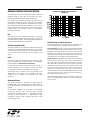
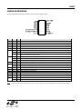
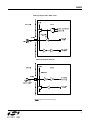
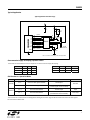
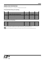
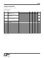
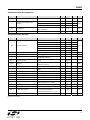
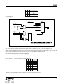
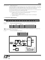
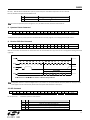
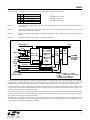
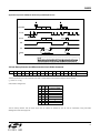
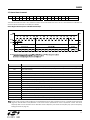
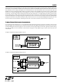
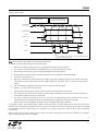
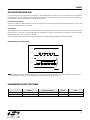
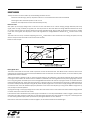
Si4421 Universal ISM Band FSK Transceiver Si4421 PIN ASSIGNMENT DESCRIPTION Silicon Labs’ Si4421 is a single chip, low power, multi-channel FSK transceiver designed for use in applications requiring FCC or ETSI conformance for unlicensed use in the 433, 868 and 915 MHz bands. The Si4421 transceiver is a part of Silicon Labs’ EZRadioTM product line, which produces a flexible, low cost, and highly integrated solution that does not require production alignments. The chip is a complete analog RF and baseband transceiver including a multi-band PLL synthesizer with PA, LNA, I/Q down converter mixers, baseband filters and amplifiers, and an I/Q demodulator. All required RF functions are integrated. Only an external crystal and bypass filtering are needed for operation. The Si4421 features a completely integrated PLL for easy RF design, and its rapid settling time allows for fast frequency-hopping, bypassing multipath fading and interference to achieve robust wireless links. The PLL’s high resolution allows the usage of multiple channels in any of the bands. The receiver baseband bandwidth (BW) is programmable to accommodate various deviation, data rate and crystal tolerance requirements. The transceiver employs the Zero-IF approach with I/Q demodulation. Consequently, no external components (except crystal and decoupling) are needed in most applications. The Si4421 dramatically reduces the load on the microcontroller with the integrated digital data processing features: data filtering, clock recovery, data pattern recognition, integrated FIFO and TX data register. The automatic frequency control (AFC) feature allows the use of a low accuracy (low cost) crystal. To minimize the system cost, the Si4421 can provide a clock signal for the microcontroller, avoiding the need for two crystals. For low power applications, the Si4421 supports low duty cycle operation based on the internal wake-up timer. FUNCTIONAL BLOCK DIAGRAM MIX I AMP OC 7 clk RF1 13 RF2 12 MIX Q AMP Data Filt CLK Rec I/Q DEMOD Self cal. LNA data OC PA FIFO RSSI PLL & I/Q VCO with cal. RF Parts COMP DQD AFC BB Amp/Filt./Limiter CLK div Xosc WTM with cal. Data processing units 6 DCLK / CFIL / FFIT / FSK / DATA / nFFS This document refers to Si4421-IC rev A1. See www.silabs.com/integration for any applicable errata. See back page for ordering information. FEATURES Fully integrated (low BOM, easy design-in) No alignment required in production Fast-settling, programmable, high-resolution PLL synthesizer Fast frequency-hopping capability High bit rate (up to 115.2 kbps in digital mode and 256 kbps in analog mode) Direct differential antenna input/output Integrated power amplifier Programmable TX frequency deviation (15 to 240 kHz) Programmable RX baseband bandwidth (67 to 400 kHz) Analog and digital RSSI outputs Automatic frequency control (AFC) Data quality detection (DQD) Internal data filtering and clock recovery RX synchron pattern recognition SPI compatible serial control interface Clock and reset signals for microcontroller 16-bit RX Data FIFO Two 8-bit TX data registers Low power duty cycle mode Standard 10 MHz crystal reference with on-chip tuning Wake-up timer 2.2 to 3.8 V supply voltage Low power consumption Low standby current (0.3 A) Compact 16 pin TSSOP package Supports very short packets (down to 3 bytes) Excellent temperature stability of the RF parameters Good adjacent channel rejection/blocking TYPICAL APPLICATIONS LBD Controller Bias Low Power parts 8 9 15 1 2 CLK XTL / REF ARSSI SDI SCK 3 4 nSEL SDO 5 10 16 11 14 nIRQ nRES nINT / VDI VSS VDD Home security and alarm Remote control, keyless entry Wireless keyboard/mouse and other PC peripherals Toy controls Remote keyless entry Tire pressure monitoring Telemetry Personal/patient data logging Remote automatic meter reading 1 Si4421-DS rev 2.4r 0708 www.silabs.com Si4421 DETAILED FEATURE-LEVEL DESCRIPTION Full Baseband Amplifier Transfer Function BW=67kHz The Si4421 FSK transceiver is designed to cover the unlicensed frequency bands at 433, 868 and 915 MHz. The device facilitates compliance with FCC and ETSI requirements. The receiver block employs the Zero-IF approach with I/Q demodulation, allowing the use of a minimal number of external components in a typical application. The Si4421 incorporates a fully integrated multi-band PLL synthesizer, PA with antenna tuning, an LNA with switchable gain, I/Q down converter mixers, baseband filters and amplifiers, and an I/Q demodulator followed by a data filter. PLL The programmable PLL synthesizer determines the operating frequency, while preserving accuracy based on the on-chip crystalcontrolled reference oscillator. The PLL’s high resolution allows the usage of multiple channels in any of the bands. RF Power Amplifier (PA) The power amplifier has an open-collector differential output and can directly drive different PCB antennas with a programmable output power level. An automatic antenna tuning circuit is built in to avoid costly trimming procedures and the so-called “hand effect”. LNA The LNA has approximately 250 Ohm input impedance, which functions well with the proposed antennas (see: Application Notes available from www.silabs.com/integration) If the RF input of the chip is connected to 50 Ohm devices, an external matching circuit is required to provide the correct matching and to minimize the noise figure of the receiver. The LNA gain can be selected in four steps (between 0 and -20dB relative to the highest gain) according to RF signal strength. It can be useful in an environment with strong interferers. Baseband Filters Data Filtering and Clock Recovery Output data filtering can be completed by an external capacitor or by using digital filtering according to the final application. Analog operation: The filter is an RC type low-pass filter followed by a Schmitt-trigger (St). The resistor (10 kOhm) and the St are integrated on the chip. An (external) capacitor can be chosen according to the actual bit rate. In this mode, the receiver can handle up to 256 kbps data rate. The FIFO cannot be used in this mode and clock is not provided for the demodulated data. Digital operation: A digital filter is used with a clock frequency at 29 times the bit rate. In this mode, there is a clock recovery circuit (CR), which can provide synchronized clock to the data. Using this clock the received data can fill a FIFO. The CR has three operation modes: fast, slow, and automatic. In slow mode, its noise immunity is very high, but it has slower settling time and requires more accurate data timing than in fast mode. In automatic mode, the CR automatically changes between fast and slow mode. The CR starts in fast mode, then after locking, it automatically switches to slow mode (Only the digital data filter and the clock recovery use the bit rate clock. For analog operation, there is no need for setting the correct bit rate.) The receiver bandwidth is selectable by programming the bandwidth (BW) of the baseband filters. This allows setting up the receiver according to the characteristics of the signal to be received. An appropriate bandwidth can be chosen to accommodate various FSK deviation, data rate and crystal tolerance requirements. The filter structure is 7th order Butterworth lowpass with 40 dB suppression at 2 · BW frequency. Offset cancellation is done by using a high-pass filter with a cut-off frequency below 7 kHz. 2 Si4421 Data Validity Blocks RSSI A digital RSSI output is provided to monitor the input signal level. It goes high if the received signal strength exceeds a given preprogrammed level. An analog RSSI signal is also available. The RSSI settling time depends on the external filter capacitor. Pin 15 is used as analog RSSI output. The digital RSSI can be monitored by reading the status register. Typical Analog ARSSI Voltage vs. RF Input Power suggested to turn the output buffer off by the Power Management Command (page 15). Low Battery Voltage Detector The low battery detector circuit monitors the supply voltage and generates an interrupt if it falls below a programmable threshold level. The detector circuit has 50 mV hysteresis. Wake-Up Timer The wake-up timer has very low current consumption (1.5 µA typical) and can be programmed from 1 ms to several days with an accuracy of ±10%. The wake-up timer calibrates itself to the crystal oscillator at every startup. For proper calibration of the wake-up timer the crystal oscillator must be running before the wake-up timer is enabled. The calibration process takes approximately 0.5ms. For the crystal start up time (tsx), see page 11. Event Handling DQD The operation of the Data Quality Detector is based on counting the spikes on the unfiltered received data. High output signal indicates an operating FSK transmitter within baseband filter bandwidth from the local oscillator. DQD threshold parameter can be set by using the Data Filter Command (page 19). AFC By using an integrated Automatic Frequency Control (AFC) feature, the receiver can minimize the TX/RX offset in discrete steps, allowing the use of: Narrower receiver bandwidth (i.e. increased sensitivity) Higher data rate Inexpensive crystals Crystal Oscillator The Si4421 has a single-pin crystal oscillator circuit, which provides a 10 MHz reference signal for the PLL. To reduce external parts and simplify design, the crystal load capacitor is internal and programmable. Guidelines for selecting the appropriate crystal can be found later in this datasheet. The transceiver can supply a clock signal for the microcontroller; so accurate timing is possible without the need for a second crystal. When the microcontroller turns the crystal oscillator off by clearing the appropriate bit using the Power Management Command (page 15), the chip provides a fixed number (192) of further clock pulses (“clock tail”) for the microcontroller to let it go to idle or sleep mode. If this clock output is not used, it is In order to minimize current consumption, the transceiver supports different power saving modes. Active mode can be initiated by several wake-up events (negative logical pulse on nINT input, wake-up timer timeout, low supply voltage detection, on-chip FIFO filled up or receiving a request through the serial interface). If any wake-up event occurs, the wake-up logic generates an interrupt signal, which can be used to wake up the microcontroller, effectively reducing the period the microcontroller has to be active. The source of the interrupt can be read out from the transceiver by the microcontroller through the SDO pin. Interface and Controller An SPI compatible serial interface lets the user select the frequency band, center frequency of the synthesizer, and the bandwidth of the baseband signal path. Division ratio for the microcontroller clock, wake-up timer period, and low supply voltage detector threshold are also programmable. Any of these auxiliary functions can be disabled when not needed. All parameters are set to default after power-on; the programmed values are retained during sleep mode. The interface supports the read-out of a status register, providing detailed information about the status of the transceiver and the received data. The transmitter block is equipped with two 8-bit wide TX data registers. It is possible to write 8 bits into the register in burst mode and the internal bit rate generator transmits the bits out with the predefined rate. For further details, see the TX Register Buffered Data Transmission section (page 28). It is also possible to store the received data bits into a FIFO register and read them out in a buffered mode. 3 Si4421 PACKAGE PIN DEFINITIONS Pin type key: D=digital, A=analog, S=supply, I=input, O=output, IO=input/output Pin Name Type 1 SDI DI Data input of the serial control interface 2 SCK DI Clock input of the serial control interface 3 nSEL DI Chip select input of the serial control interface (active low) 4 SDO DO Serial data output with bus hold 5 nIRQ DO Interrupt request output (active low) FSK DI Transmit FSK data input (internal pull up resistor 133 k) 6 DATA DO Received data output (FIFO not used) nFFS DI FIFO select input (active low). In FIFO mode, when bit ef is set in Configuration Setting Command, page 15 (internal pull up resistor 133 k) 7 8 Function DLCK DO Received data clock output (Digital filter used, FIFO not used) CFIL AIO External data filter capacitor connection (Analog filter used) FFIT DO FIFO interrupt (active high). In FIFO mode, when bit ef is set in Configuration Setting Command CLK DO Microcontroller clock output XTL AIO Crystal connection (the other terminal of crystal to VSS) or external reference input REF AIO External reference input. Use 33 pF series coupling capacitor 10 nRES DIO Open drain reset output with internal pull-up and input buffer (active low) 11 VSS S 12 RF2 AIO 13 RF1 AIO 14 VDD S 15 ARSSI AO Analog RSSI output nINT DI Interrupt input (active low) VDI DO Valid data indicator output 9 16 Ground reference voltage RF differential signal input/output RF differential signal input/output Positive supply voltage Note: The actual mode of the multipurpose pins (pin 6 and 7) is determined by the TX/RX data I/O settings of the transceiver. 4 Si4421 Internal Pin Connections Pin Name 1 SDI 2 SCK 3 nSEL 4 SDO 5 Internal connection Pin Name 10 nRES 11 VSS 12 RF2 13 RF1 14 VDD 15 ARSSI Internal connection VDD PAD 1.5k VSS nIRQ FSK 6 DATA nFFS DLCK 7 CFIL FFIT VDD 8 CLK nINT 16 PAD 10 VDI VSS XTL 9 REF 5 Si4421 PIN6 Logic Diagram (FSK / DATA / nFFS) PIN10 Logic Diagram (nRES I/O) * Note: These pins can be left floating. 6 Si4421 Typical Application Typical application with FIFO usage VDD C1 2.2u C3 P7 P6 P5 P4 P3 P2 P1 P0 CLKin nRESin VDI (optional) 1 SDI SCK 2 3 nSEL SDO nIRQ nFFS (optional)* FFIT (optional)* (optional) CLK nRES 4 5 6 7 8 Si4421 (optional) 16 15 14 13 TP C2 10n C4 2.2n (opt.) 12 11 10 9 PCB Antenna X1 10MHz Note: * Connections needed only in time critical applications Recommended supply decoupling capacitor values C2 and C3 should be 0603 size ceramic capacitors to achieve the best supply decoupling. Band [MHz] C1 C2 C3 Property C1 C2 C3 433 2.2µF 10nF 220pF SMD size A 0603 0603 868 2.2µF 10nF 47pF Dielectric Tantalum Ceramic Ceramic 915 2.2µF 10nF 33pF Pin Function vs. Operation Mode Mode Bit setting Function Pin 6 el = 0 Internal TX data register disabled TX data input el = 1 Internal TX data register enabled nFFS input (TX data register can be accessed) ef = 0 Receiver FIFO disabled RX data output RX data clock output ef = 1 Receiver FIFO disabled nFFS input (RX data FIFO can be accessed) FFIT output Transmit Receive Pin 7 Not used The el and ef bits can be found in the Configuration Setting Command on page 15. Bit el enables the internal TX data register. Bit ef enables the FIFO mode. 7 Si4421 GENERAL DEVICE SPECIFICATIONS All voltages are referenced to V ss , the potential on the ground reference pin VSS. Absolute Maximum Ratings (non-operating) Symbol Parameter Min Max Units V dd Positive supply voltage V in Voltage on any pin (except RF1 and RF2) -0.5 6 V -0.5 V dd +0.5 V oc V Voltage on open collector outputs (RF1, RF2) -0.5 V dd +1.5 (Note 1) V I in Input current into any pin except VDD and VSS -25 25 mA ESD Electrostatic discharge with human body model T st Storage temperature T ld Lead temperature (soldering, max 10 s) 1000 -55 V 125 o 260 o C C Recommended Operating Range Symbol Parameter Min Max Units V dd Positive supply voltage 2.2 3.8 V V oc Voltage range on open collector outputs (RF1, RF2) V dd -1.5 (Note 2) V dd +1.5 T op Ambient operating temperature -40 85 V o C Note 1: The voltage on RF1 and RF2 pins can be higher than the actual V dd but cannot exceed 7 V. Note 2: The actual voltage on RF1 and RF2 pins can be lower than the current V dd but never should go below 1.2 V. 8 Si4421 ELECTRICAL SPECIFICATION Test Conditions: T op = 27 oC; V dd = V oc = 3.3 V DC Characteristics Symbol I dd_TX_0 I dd_TX_PMAX I dd_RX Parameter Supply current (TX mode, P out = 0 dBm) Supply current (TX mode, P out = P max ) Supply current (RX mode) I pd Standby current (Sleep mode) I lb Low battery voltage detector current consumption Conditions/Notes 16 17 433 MHz band 22 26 868 MHz band 23 27 915 MHz band 24 28 433 MHz band 11 13 868 MHz band 12 14 915 MHz band 13 15 All blocks disabled 0.3 1 µA 0.5 1.7 µA Wake-up timer current consumption Crystal oscillator on (Note 1) Programmable in 0.1 V steps Low battery detect threshold V il Digital input low level voltage V ih Digital input high level voltage I il Digital input current Units 915 MHz band Idle current Low battery detection accuracy Max 868 MHz band Ix V lb Typ 15 I wt V lba Min 433 MHz band mA 1.5 3.5 µA 1.2 mA 3.75 ±3 -1 I ih Digital input current V ih = V dd , V dd = 3.8 V V ol Digital output low level I ol = 2 mA V oh Digital output high level I oh = -2 mA V dd -0.4 V % 0.3·V dd V 1 µA 1 µA 0.4 V 0.7·V dd -1 mA 0.6 2.25 V il = 0 V mA V V Notes are on page 12. 9 Si4421 AC Characteristics (PLL parameters) Symbol Parameter Conditions/Notes f ref PLL reference frequency (Note 2) fo Receiver LO/Transmitter carrier frequency Min Typ Max Units 9 10 11 MHz 433 MHz band, 2.5 kHz resolution 430.24 439.75 868 MHz band, 5.0 kHz resolution 860.48 879.51 915 MHz band, 7.5 kHz resolution 900.72 929.27 MHz t lock PLL lock time Frequency error < 1kHz after 10 MHz step 30 t stP PLL startup time (Note 10) With a running crystal oscillator 200 300 µs Typ Max Units µs AC Characteristics (Receiver) Symbol BW Parameter Receiver bandwidth Conditions/Notes Min mode 0 67 mode 1 134 mode 2 200 mode 3 270 mode 4 340 mode 5 400 0.6 kHz BR RX FSK bit rate (Note 10) With internal digital filters BRA RX FSK bit rate (Note 10) With analog filter 115.2 kbps 256 kbps P min Receiver Sensitivity BER 10 , BW=67 kHz, BR=1.2 kbps, 868 MHz Band (Note 3) AFC range AFC locking range δf FSK : FSK deviation in the received signal IIP3 inh Input IP3 In band interferers in high bands (868 MHz, 915 MHz) -21 dBm IIP3 outh Input IP3 Out of band interferers l f-f o l > 4 MHz -18 dBm IIP3 (LNA –6 dB gain) In band interferers in low band (433 MHz) -15 dBm -3 IIP3 inl IIP3 outl IIP3 (LNA –6 dB gain) Out of band interferers l f-f o l > 4 MHz P max Maximum input power LNA: high gain Cin RF input capacitance RS a RS r -110 dBm 0.8·δf FSK -12 dBm 0 dBm 1 pF RSSI accuracy ±6 dB RSSI range 46 dB +35 mV/V 6 dB 500 µs RS ps RSSI power supply dependency C ARSSI Filter capacitor for ARSSI RS step RSSI programmable level steps RS resp DRSSI response time P sp_rx Receiver spurious emission When input signal level lower than -54 dBm and greater than -100 dBm 1 Until the RSSI signal goes high after the input signal exceeds the preprogrammed limit C ARRSI = 4.7 nF nF -60 dBm Notes are on page 12. 10 Si4421 AC Characteristics (Transmitter) Symbol Parameter Conditions/Notes Min Open collector output DC current Programmable 0.5 P max_50 Max. output power delivered to 50 Ohm load over a suitable matching network (Note 4) In 433 MHz band 7 In 868 MHz / 915 MHz bands 5 P max_ant Max. EIRP with suitable selected PCB antenna (Note 6) In 433 MHz band with monopole antenna with matching network (Note 4) 7 In 868 MHz / 915 MHz bands (Note 5) 7 I OUT Typ Units 6 mA dBm dBm P out Typical output power Selectable in 2.5 dB steps (Note 7) P sp Spurious emission l f-f sp l > 1 MHz At max power 50 Ohm load (Note 4) -55 With PCB antenna (Note 5) -60 P harm Harmonic suppression Co Output capacitance (set by the automatic antenna tuning circuit) Qo Quality factor of the output capacitance L out Output phase noise P max -17.5 Max P max At max power 50 Ohm load (Note 4) -35 With PCB antenna (Note 5) -42 In 433 MHz band 2 2.6 3.2 In 868 MHz / 915 MHz bands 2.1 2.7 3.3 In 433 MHz band 13 15 17 In 868 MHz / 915 MHz bands 8 10 12 100 kHz from carrier, in 868 MHz band -80 1 MHz from carrier, in 868 MHz band -103 dBm dBc dBc pF dBc/Hz BR TX FSK bit rate Via internal TX data register 172 kbps BRA TX FSK bit rate TX data connected to the FSK input 256 kbps FSK frequency deviation Programmable in 15 kHz steps 240 kHz df fsk 15 AC Characteristics (Turn-on/Turnaround timings) Symbol Parameter Conditions/Notes Typ Max Units Crystal oscillator startup time Default capacitance bank setting, crystal ESR < 50 Ohm (Note 9). Crystal load capacitance = 16 pF. 2 7 ms T tx_XTAL_ON Transmitter turn-on time Synthesizer off, crystal oscillator on with 10 MHz step 250 µs T rx_XTAL_ON Receiver turn-on time Synthesizer off, crystal oscillator on with 10 MHz step 250 µs T tx_rx_SYNT_ON Transmitter – Receiver turnover time Synthesizer and crystal oscillator on during TX/RX change with 10 MHz step 150 µs T rx_tx_SYNT_ON Receiver – Transmitter turnover time Synthesizer and crystal oscillator on during RX/TX change with 10 MHz step 150 µs t sx Min AC Characteristics (Others) Symbol Parameter Conditions/Notes Min C xl Crystal load capacitance, see crystal selection guide Programmable in 0.5 pF steps, tolerance ± 10% 8.5 t POR Internal POR timeout After V dd has reached 90% of final value (Note 8) t PBt Wake-up timer clock accuracy Crystal oscillator must be enabled to ensure proper calibration at the start up. (Note 9) C inD Digital input capacitance tr, tf Digital output rise/fall time 15 pF pure capacitive load Typ Max Units 16 pF 100 ms ± 10 % 2 pF 10 ns Notes are on page 12. 11 Si4421 Note 1: Measured with disabled clock output buffer Note 2: Not using a 10 MHz crystal is allowed but not recommended because all crystal referred timing and frequency parameters will change accordingly Note 3: See the BER diagrams in the measurement results section (page 37) for detailed information Note 4: See reference design with 50 Ohm Matching Network (page 39) for details Note 5: See reference design with Resonant PCB Antenna (BIFA) on page 41 for details Note 6: Optimal antenna admittance/impedance: Si4421 Y antenna [mS] Z antenna [Ohm] L antenna [nH] 2 – j5.9 52 + j152 62 868 MHz 1.2 - j11.9 7.8 + j83 15.4 915 MHz 1.49 - j12.8 9 + j77 13.6 433 MHz Note 7: Adjustable in 8 steps Note 8: During the Power-On Reset period, commands are not accepted by the chip. In case of software reset (see Wake-Up Timer Command, page 25) the reset timeout is 0.25ms typical. Note 9: The crystal oscillator start up time strongly depends on the capacitance seen by the oscillator. Low capacitance and low ESR crystal is recommended with low parasitic PCB layout design. Note 10: By design 12 Si4421 CONTROL INTERFACE Commands to the transmitter are sent serially. Data bits on pin SDI are shifted into the device upon the rising edge of the clock on pin SCK whenever the chip select pin nSEL is low. When the nSEL signal is high, it initializes the serial interface. All commands consist of a command code, followed by a varying number of parameter or data bits. All data are sent MSB first (e.g. bit 15 for a 16bit command). Bits having no influence (don’t care) are indicated with X. Special care must be taken when the microcontroller’s builtin hardware serial port is used. If the port cannot be switched to 16-bit mode then a separate I/O line should be used to control the nSEL pin to ensure the low level during the whole duration of the command or a software serial control interface should be implemented. The Power-On Reset (POR) circuit sets default values in all control and command registers. The receiver will generate an interrupt request (IT) for the microcontroller - by pulling the nIRQ pin low - on the following events: The TX register is ready to receive the next byte (RGIT) The RX FIFO has received the preprogrammed amount of bits (FFIT) Power-on reset (POR) RX FIFO overflow (FFOV) / TX register underrun (RGUR) Wake-up timer timeout (WKUP) Negative pulse on the interrupt input pin nINT (EXT) Supply voltage below the preprogrammed value is detected (LBD) FFIT and FFOV are applicable when the RX FIFO is enabled. RGIT and RGUR are applicable only when the TX register is enabled. To identify the source of the IT, the status bits should be read out. Timing Specification Symbol Parameter Minimum value [ns] t CH Clock high time 25 t CL Clock low time 25 t SS Select setup time (nSEL falling edge to SCK rising edge) 10 t SH Select hold time (SCK falling edge to nSEL rising edge) 10 t SHI Select high time 25 t DS Data setup time (SDI transition to SCK rising edge) 5 t DH Data hold time (SCK rising edge to SDI transition) 5 t OD Data delay time 10 Timing Diagram tSHI tSS nSEL tCH tOD tCL tSH SCK tDS tDH SDI BIT 15 SDO FFIT BIT 14 FFOV BIT 13 BIT 8 CRL BIT 7 AT S BIT 1 OFFS(0) BIT 0 FIFO OUT 13 Si4421 Control Commands Control Command Related Parameters/Functions Related control bits 1 Configuration Setting Command Frequency band, crystal oscillator load capacitance, RX FIFO and TX register enable el, ef, b1 to b0, x3 to x0 2 Power Management Command Receiver/Transmitter mode change, synthesizer, crystal oscillator, PA, wake-up timer, clock output enable er, ebb, et, es, ex, eb, ew, dc 3 Frequency Setting Command Frequency of the local oscillator/carrier signal f11 to f0 4 Data Rate Command Bit rate cs, r6 to r0 5 Receiver Control Command Function of pin 16, Valid Data Indicator, baseband bandwidth, LNA gain, digital RSSI threshold p16, d1 to d0, i2 to i0, g1 to g0, r2 to r0 6 Data Filter Command Data filter type, clock recovery parameters al, ml, s, f2 to f0 7 FIFO and Reset Mode Command Data FIFO IT level, FIFO start control, FIFO enable and FIFO fill enable, POR sensitivity f3 to f0, sp, ff, al, dr 8 Synchron Pattern Command Synchron pattern b7 to b0 9 Receiver FIFO Read Command RX FIFO read 10 AFC Command AFC parameters a1 to a0, rl1 to rl0, st, fi, oe, en 11 TX Configuration Control Command Modulation parameters, output power mp, m3 to m0, p2 to p0 12 PLL Setting Command CLK out buffer speed, dithering, PLL bandwidth ob1 to ob0, ddit, dly, bw0 13 Transmitter Register Write Command TX data register write t7 to t0 14 Wake-Up Timer Command Wake-up time period r4 to r0, m7 to m0 15 Low Duty-Cycle Command Enable and set low duty-cycle mode d6 to d0, en 16 Low Battery Detector and Microcontroller Clock Divider Command LBD voltage and microcontroller clock division ratio d2 to d0, v3 to v0 17 Status Read Command Status bit readout In general, setting the given bit to one will activate the related function. In the following tables, the POR column shows the default values of the command registers after power-on. Control Register Default Values Control Register Power-On Reset Value 1 Configuration Setting Command 2 Power Management Command 8008h 8208h 3 Frequency Setting Command A680h 4 Data Rate Command C623h 5 Receiver Control Command 9080h 6 Data Filter Command C22Ch 7 FIFO and Reset Mode Command CA80h 8 Synchron Pattern Command CED4h 9 Receiver FIFO Read Command B000h 10 AFC Command C4F7h 11 TX Configuration Control Command 9800h 12 PLL Setting Command CC77h 13 Transmitter Register Write Command B8AAh 14 Wake-Up Timer Command E196h 15 Low Duty-Cycle Command C80Eh 16 Low Battery Detector and Microcontroller Clock Divider Command C000h 17 Status Read Command 0000h 14 Si4421 Description of the Control Commands 1. Configuration Setting Command Bit 15 14 13 12 11 10 9 8 7 6 5 4 3 2 1 0 POR 1 0 0 0 0 0 0 0 el ef b1 b0 x3 x2 x1 x0 8008h Bit el enables the internal data register. Bit ef enables the FIFO mode. If ef = 0 then DATA (pin 6) and DCLK (pin 7) are used for data and data clock output. b1 0 0 1 1 b0 0 1 0 1 x3 0 0 0 0 Frequency Band Reserved 433 868 915 x2 0 0 0 0 x1 0 0 1 1 x0 0 1 0 1 Crystal Load Capacitance [pF] 8.5 9.0 9.5 10.0 … 1 1 1 1 1 1 0 1 15.5 16.0 2. Power Management Command Bit 15 14 13 12 11 10 9 8 7 6 5 4 3 2 1 0 POR 1 0 0 0 0 0 1 0 er ebb et es ex eb ew dc 8208h Bit Function of the control bit Related blocks er Enables the whole receiver chain RF front end, baseband, synthesizer, crystal oscillator The receiver baseband circuit can be separately switched on Baseband et Switches on the PLL, the power amplifier, and starts the transmission (If TX register is enabled) Power amplifier, synthesizer, crystal oscillator es Turns on the synthesizer Synthesizer ex Turns on the crystal oscillator Crystal oscillator ebb eb Enables the low battery detector Low battery detector ew Enables the wake-up timer Wake-up timer dc Disables the clock output (pin 8) Clock output buffer The ebb, es, and ex bits are provided to optimize the TX to RX or RX to TX turnaround time. The RF frontend consist of the LNA (low noise amplifier) and the mixer. The synthesizer block has two main components: the VCO and the PLL. The baseband section contains the baseband amplifier, low pass filter, limiter and the I/Q demodulator. To decrease TX/RX turnaround time, it is possible to leave the baseband section powered on. Switching to RX mode means disabling the PA and enabling the RF frontend. Since the baseband block is already on, the internal startup calibration will not be performed, the turnaround time will be shorter. The synthesizer also has an internal startup calibration procedure. If quick RX/TX switching needed it may worth to leave this block on. Enabling the transmitter using the et bit will turn on the PA, the synthesizer is already up and running. The power amplifier almost immediately produces TX signal at the output. The crystal oscillator provides reference signal to the RF synthesizer, the baseband circuits and the digital signal processor part. When the receiver or the transmitter part frequently used, it is advised to leave the oscillator running because the crystal might need a few milliseconds to start. This time mainly depends on the crystal parameters. It is important to note that leaving blocks unnecessary turned on can increase the current consumption thus decreasing the battery life. 15 Si4421 Logic connections between power control bits: enable power amplifier et start TX Edge detector enable power amplifier enable RF front end clear TX latch es enable RF synthesizer er enable RF front end enable RF synthesizer VCO and PLL start TX clear TX latch enable crystal oscillator enable baseband circuits TX latch Crystal oscillator enable baseband circuits I/Q demod ebb Digital signal processing enable crystal oscillator ex clock and data out Note: If both et and er bits are set the chip goes to receive mode. FSK / nFFS input are equipped with internal pull-up resistor. To achieve minimum current consumption do not pull this input to logic low in sleep mode. To enable the RF synthesizer, the crystal oscillator must be turned on To turn on the baseband circuits, the RF synthesizer (and this way the crystal oscillator) must be enabled. Setting the er bit automatically turns on the crystal oscillator, the synthesizer, the baseband circuits and the RF fronted. Setting the et bit automatically turns on the crystal oscillator, the synthesizer and the RF power amplifier. Clock tail feature: When the clock output (pin 8) used to provide clock signal for the microcontroller (dc bit is set to 0), it is possible to use the clock tail feature. This means that the crystal oscillator turn off is delayed, after issuing the command (clearing the ex bit) 192 more clock pulses are provided. This ensures that the microcontroller can switch itself to low power consumption mode. In order to use this feature, a Status Read Command (page 27) must be issued before the ex bit set to zero. If status read was not performed then the clock output shuts down immediately leaving the microcontroller in unknown state. Automatic crystal oscillator enable/disable feature: When an interrupt occurs, the crystal oscillator automatically turns on – regardless to the setting of the ex bit – to supply clock signal to the microcontroller. After clearing all interrupts by handling them properly (see the Interrupt Handling section, page 28) and performing Status Read Command, the crystal oscillator is automatically turned off. The clock tail feature provides enough clock pulses for the microcontroller to go to low power mode. Due to this automatic feature, it is not possible to turn off the crystal by clearing the ex bit if any interrupt is active. For example, after power on the POR interrupt must be cleared by a status read then writing zero to the ex bit will put the part into sleep mode. Very important to clear all interrupts before turning the ex bit off because the extra current required by running crystal oscillator can shorten the battery life significantly. Disabling the clock output (bit dc=1) turns off both the clock tail and the automatic crystal oscillator enable/disable feature, only the ex bit controls the crystal oscillator (supposing that both the er and et bits are cleared), the interrupts have no effect on it. 16 Si4421 3. Frequency Setting Command Bit 15 14 13 12 11 10 9 8 7 6 5 4 3 2 1 0 POR 1 0 1 0 f11 f10 f9 f8 f7 f6 f5 f4 f3 f2 f1 f0 A680h The constants C1 and C2 are determined by the selected band as: The 12-bit parameter F (bits f11 to f0) should be in the range of 96 and 3903. When F value sent is out of range, the previous value is kept. The synthesizer center frequency f 0 can be calculated as: Band [MHz] C1 C2 433 1 43 868 2 43 915 3 30 f 0 = 10 · C1 · (C2 + F/4000) [MHz] Band Minimum Frequency Maximum Frequency 433 MHz 430.2400 MHz 439.7575 MHz PLL Frequency Step 2.5 kHz 868 MHz 860.4800 MHz 879.5150 MHZ 5.0 kHz 915 MHz 900.7200 MHz 929.2725 MHz 7.5 kHz 4. Data Rate Command Bit 15 14 13 12 11 10 9 8 7 6 5 4 3 2 1 0 POR 1 1 0 0 0 1 1 0 cs r6 r5 r4 r3 r2 r1 r0 C623h The actual bit rate in transmit mode and the expected bit rate of the received data stream in receive mode is determined by the 7-bit parameter R (bits r6 to r0) and bit cs. BR = 10000 / 29 / (R+1) / (1+cs · 7) [kbps] In the receiver set R according to the next function: R= (10000 / 29 / (1+cs · 7) / BR) – 1, where BR is the expected bit rate in kbps. Apart from setting custom values, the standard bit rates from 600 bps to 115.2 kbps can be approximated with small error. Data rate accuracy requirements: Clock recovery in slow mode: BR/BR < 1/(29 · N bit ) Clock recovery in fast mode: BR/BR < 3/(29 · N bit ) BR is the bit rate set in the receiver and BR is the bit rate difference between the transmitter and the receiver. N bit is the maximum number of consecutive ones or zeros in the data stream. It is recommended for long data packets to include enough 1/0 and 0/1 transitions, and to be careful to use the same division ratio in the receiver and in the transmitter. 5. Receiver Control Command Bit 15 14 13 12 11 10 9 8 7 6 5 4 3 2 1 0 POR 1 0 0 1 0 p16 d1 d0 i2 i1 i0 g1 g0 r2 r1 r0 9080h Bit 10 (p16): Pin 16 function select p16 0 1 Function of pin 16 Interrupt input VDI output 17 Si4421 Bits 9-8 (d1 to d0): VDI (valid data indicator) signal response time setting: d1 0 0 1 1 d0 0 1 0 1 Response Fast Medium Slow Always on VDI Logic Diagram: MUX DQD CR_LOCK d0 d1 DRSSI MEDIUM SEL0 SEL1 FAST SLOW DQD LOGIC HIGH IN0 IN1 Y VDI IN2 IN3 CLR DRSSI DQD CR_LOCK SET Q er * R/S FF CLR Note: * For details see the Power Management Command Slow mode: The VDI signal will go high only if the DRSSI, DQD and the CR_LOCK (Clock Recovery Locked) signals present at the same time. It stays high until any of the abovementioned signals present; it will go low when all the three input signals are low. Medium mode: The VDI signal will be active when the CR_LOCK signal and either the DRSSI or the DQD signal is high. The valid data indicator will go low when either the CR_LOCK gets inactive or both of the DRSSI or DQD signals go low. Fast mode: The VDI signal follows the level of the DQD signal. Always mode: VDI is connected to logic high permanently. It stays always high independently of the receiving parameters. Bits 7-5 (i2 to i0): Receiver baseband bandwidth (BW) select: i2 0 0 0 0 1 1 1 1 i1 0 0 1 1 0 0 1 1 i0 0 1 0 1 0 1 0 1 BW [kHz] Reserved 400 340 270 200 134 67 Reserved Note: For the optimal bandwidth settings at different data rates see the table on page 37. 18 Si4421 Bits 4-3 (g1 to g0): LNA gain select: g1 0 0 1 1 Bits 2-0 (r2 to r0): g0 0 1 0 1 Gain relative to maximum [dB] 0 -6 -14 -20 RSSI detector threshold: r2 0 0 0 0 1 1 1 1 r1 0 0 1 1 0 0 1 1 RSSI setth -103 -97 -91 -85 -79 -73 Reserved Reserved r0 0 1 0 1 0 1 0 1 The RSSI threshold depends on the LNA gain, the real RSSI threshold can be calculated: RSSI th =RSSI setth +G LNA 6. Data Filter Command Bit 15 14 13 12 11 10 9 8 7 6 5 4 3 2 1 0 POR 1 1 0 0 0 0 1 0 al ml 1 s 1 f2 f1 f0 C22Ch Bit 7 (al): Clock recovery (CR) auto lock control 1: auto mode: the CR starts in fast mode, after locking it switches to slow mode. Bit 6 (ml) has no effect. 0: manual mode, the clock recovery mode is set by Bit 6 (ml) Bit 6 (ml): Clock recovery lock control 1: fast mode, fast attack and fast release (4 to 8-bit preamble (1010...) is recommended) 0: slow mode, slow attack and slow release (12 to 16-bit preamble is recommended) Using the slow mode requires more accurate bit timing (see Data Rate Command, page 17). Bit 4 (s): Select the type of the data filter: s 0 1 Filter Type Digital filter Analog RC filter Digital: This is a digital realization of an analog RC filter followed by a comparator with hysteresis. The time constant is automatically adjusted to the bit rate defined by the Data Rate Command (page 17). Note: Bit rate cannot exceed 115 kpbs in this mode. Analog RC filter: The demodulator output is fed to pin 7 over a 10 kOhm resistor. The filter cut-off frequency is set by the external capacitor connected to this pin and VSS. The table shows the optimal filter capacitor values for different data rates Data Rate [kbps] 1.2 2.4 4.8 9.6 19.2 38.4 57.6 115.2 256 Filter Capacitor Value 12 nF 8.2 nF 6.8 nF 3.3 nF 1.5 nF 680 pF 270 pF 150 pF 100 pF Note: If analog RC filter is selected the internal clock recovery circuit and the FIFO cannot be used. 19 Si4421 Bits 2-0 (f2 to f0): DQD threshold parameter. The Data Quality Detector is a digital processing part of the radio, connected to the demodulator - it is an indicator reporting the reception of an FSK modulated RF signal. It will work every time the receiver is on. Setting this parameter defines how clean incoming data stream would be stated as good data (valid FSK signal). If the internally calculated data quality value exceeds the DQD threshold parameter for five consecutive data bits for both the high and low periods, then the DQD signal goes high. The DQD parameter in the Data Filter Command should be chosen according to the following rules: The DQD parameter can be calculated with the following formula: DQD par = 4 x (deviation – TX-RX offset ) / bit rate It should be larger than 4 because otherwise noise might be treated as a valid FSK signal The maximum value is 7. 7. FIFO and Reset Mode Command Bit 15 14 13 12 11 10 9 8 7 6 5 4 3 2 1 0 POR 1 1 0 0 1 0 1 0 f3 f2 f1 f0 sp al ff dr CA80h Bits 7-4 (f3 to f0): FIFO IT level. The FIFO generates IT when the number of received data bits reaches this level. Bit 3 (sp): Select the length of the synchron pattern: sp 0 1 Byte1 2Dh Not used Byte0 (POR) D4h D4h Synchron Pattern (Byte1+Byte0) 2DD4h D4h Note: The synchron pattern consists of one or two bytes depending on the sp bit. Byte1 is fixed 2Dh, Byte0 can be programmed by the Synchron Pattern Command (page 21). Bit 2 (al): Set the input of the FIFO fill start condition: al 0 1 FIFO fill start condition Synchron pattern Always fill 20 Si4421 Bit 1 (ff): FIFO fill will be enabled after synchron pattern reception. The FIFO fill stops when this bit is cleared. Bit 0 (dr): Disables the highly sensitive RESET mode. dr Reset mode Reset triggered when 0 Sensitive reset V dd below 1.6V, V dd glitch greater than 600mV 1 Non-sensitive reset V dd below 250mV Note: To restart the synchron pattern recognition, bit 1 (ef, FIFO fill enable) should be cleared and set. 8. Synchron Pattern Command Bit 15 14 13 12 11 10 9 8 7 6 5 4 3 2 1 0 POR 1 1 0 0 1 1 1 0 b7 b6 b5 b4 b3 b2 b1 b0 CED4h The Byte0 of the synchron pattern (see FIFO and Reset Mode command, page 20) can be reprogrammed by B <b7:b0>. 9. Receiver FIFO Read Command Bit 15 14 13 12 11 10 9 8 7 6 5 4 3 2 1 0 POR 1 0 1 1 0 0 0 0 0 0 0 0 0 0 0 0 B000h With this command, the controller can read 8 bits from the receiver FIFO. Bit 6 (ef) must be set in Configuration Setting Command (page 15). Note: During FIFO access f SCK cannot be higher than f ref /4, where f ref is the crystal oscillator frequency. When the duty-cycle of the clock signal is not 50 % the shorter period of the clock pulse width should be at least 2/f ref . 10. AFC Command Bit 15 1 14 1 Bit 7-6 (a1 to a0): 13 0 12 0 11 0 10 1 9 0 8 0 7 a1 6 a0 5 rl1 4 rl0 3 st 2 fi 1 oe 0 en POR C4F7h Automatic operation mode selector: a1 0 0 1 1 a0 0 1 0 1 Operation mode Auto mode off (Strobe is controlled by microcontroller) Runs only once after each power-up Keep the f offset only during receiving (VDI=high) Keep the f offset value independently from the state of the VDI signal 21 Si4421 Bit 5-4 (rl1 to rl0): Range limit. Limits the value of the frequency offset register to the next values: rl1 0 0 1 1 rl0 0 1 0 1 Max deviation No restriction +15 f res to -16 f res +7 f res to -8 f res +3 f res to -4 f res f res : 433 MHz bands: 2.5 kHz 868 MHz band: 5 kHz 915 MHz band: 7.5 kHz Bit 3 (st): Strobe edge, when st goes to high, the actual latest calculated frequency error is stored into the offset register of the AFC block. Bit 2 (fi): Switches the circuit to high accuracy (fine) mode. In this case, the processing time is about twice as long, but the measurement uncertainty is about half. Bit 1 (oe): Enables the frequency offset register. It allows the addition of the offset register to the frequency control word of the PLL. Bit 0 (en): Enables the calculation of the offset frequency by the AFC circuit. In manual mode, the strobe signal is provided by the microcontroller. One measurement cycle (and strobe) signal can compensate about 50-60% of the actual frequency offset. Two measurement cycles can compensate 80%, and three measurement cycles can compensate 92%. The ATGL bit in the status register can be used to determine when the actual measurement cycle is finished. In automatic operation mode (no strobe signal is needed from the microcontroller to update the output offset register) the AFC circuit is automatically enabled when the VDI indicates potential incoming signal during the whole measurement cycle and the circuit measures the same result in two subsequent cycles. Without AFC the transmitter and the receiver needs to be tuned precisely to the same frequency. RX/TX frequency offset can lower the range. The units must be adjusted carefully during production, stable, expensive crystal must be used to avoid drift or the output power needs to be increased to compensate yield loss. The AFC block will calculate the TX-RX offset. This value will be used to pull the RX synthesizer close to the frequency of the transmitter. The main benefits of the automatic frequency control: cheap crystal can be used, the temperature or aging drift will not cause range loss and no production alignment needed. 22 Si4421 There are four operation modes: 1. (a1=0, a0=0) Automatic operation of the AFC is off. Strobe bit can be controlled by the microcontroller. 2. (a1=0, a0=1) The circuit measures the frequency offset only once after power up. This way, extended TX-RX distance can be achieved. In the final application, when the user inserts the battery, the circuit measures and compensates for the frequency offset caused by the crystal tolerances. This method allows for the use of cheaper quartz in the application and provides protection against tracking an interferer. 3. (a1=1, a0=0) The frequency offset is calculated automatically and the center frequency is corrected when the VDI is high. The calculated value is dropped when the VDI goes low. To improve the efficiency of the AFC calculation two methods are recommended: a. The transmit package should start with a low effective baud rate pattern (i.e.: 00110011) because it is easier to receive. The circuit automatically measures the frequency offset during this initial pattern and changes the receiving frequency accordingly. The further part of the package will be received by the corrected frequency settings. b. The transmitter sends the first part of the packet with a step higher deviation than required during normal operation to ease the receiving. After the frequency shift was corrected, the deviation can be reduced. In both cases (3a and 3b), when the VDI indicates poor receiving conditions (VDI goes low), the output register is automatically cleared. Use this “drop offset” mode when the receiver communicates with more than one transmitter. 4. (a1=1, a0=1) It is similar to mode 3, but suggested to use when a receiver operates with only one transmitter. After a complete measuring cycle, the measured value is kept independently of the state of the VDI signal. When the receiver is paired with only one transmitter, it is possible to use this “keep offset” mode. In this case, the DRSSI limit should be selected carefully to minimize the range hysteresis. 11. TX Configuration Control Command Bit 15 14 13 12 11 10 9 8 7 6 5 4 3 2 1 0 POR 1 0 0 1 1 0 0 mp m3 m2 m1 m0 0 p2 p1 p0 9800h Bits 8-4 (mp, m3 to m0): FSK modulation parameters: The resulting output frequency can be calculated as: P out f out = f 0 + (-1)SIGN · (M + 1) · (15 kHz) where: df fsk f0 is the channel center frequency (see the Frequency Setting Command) M is the four bit binary number <m3 : m0> SIGN = (mp) XOR FSK Note: f0 For the optimal FSK modulation settings at different data rates see the table on page 37. mp=0 and FSK=0 or mp=1 and FSK=1 Bits 2-0 (p2 to p0): Output power: Note: p2 p1 p0 0 0 0 0 0 0 1 -2.5 0 1 0 -5 0 1 1 -7.5 1 0 0 1 0 1 -12.5 1 1 0 -15 1 1 1 -17.5 df fsk f out mp=0 and FSK=1 or mp=1 and FSK=0 Relative Output Power [dB] Note: FSK represents the value of the actual data bit. -10 The output power given in the table is relative to the maximum available power, which depends on the actual antenna impedance. (See: Antenna Application Note: IA ISM-AN1) 23 Si4421 12. PLL Setting Command Bit 15 14 13 12 11 10 9 8 7 6 5 4 3 2 1 0 POR 1 1 0 0 1 1 0 0 0 ob1 ob0 1 dly ddit 1 bw0 CC77h Bits 6-5 (ob1-ob0): Microcontroller output clock buffer rise and fall time control. The ob1-ob0 bits are changing the output drive current of the CLK pin. Higher current provides faster rise and fall times but can cause interference. ob1 ob0 Selected µC CLK frequency 1 1 5 or 10 MHz (recommended) 1 0 3.3 MHz 0 X 2.5 MHz or less Note: Needed for optimization of the RF performance. Optimal settings can vary according to the external load capacitance. Bit 3 (dly): Switches on the delay in the phase detector when this bit is set. Bit 2 (ddit): When set, disables the dithering in the PLL loop. Bit 0 (bw0): PLL bandwidth can be set for optimal TX RF performance. bw0 Max bit rate [kbps] 0 86.2 Phase noise at 1MHz offset [dBc/Hz] -107 1 256 -102 Note: POR default settings of the register were carefully selected to cover almost all typical applications. When changing these values, examine thoroughly the output RF spectrum. For more information, contact Silicon Labs Support. 13. Transmitter Register Write Command Bit 15 14 13 12 11 10 9 8 7 6 5 4 3 2 1 0 POR 1 0 1 1 1 0 0 0 t7 t6 t5 t4 t3 t2 t1 t0 B8AAh With this command, the controller can write 8 bits (t7 to t0) to the transmitter data register. Bit 7 (el) must be set in Configuration Setting Command (page 15). Multiple Byte Write with Transmit Register Write Command: nSEL SCK SDI TX BYTE1 TX BYTE2 TX BYTEn Transmit Register Write command SDO (REGISTER IT in TX mode*) Note: *The transceiver is in transmit (TX) mode when bit er is cleared using the Power Management Command Note: Alternately the transmit register can be directly accessed by nFFS (pin6). 24 Si4421 14. Wake-Up Timer Command Bit 15 14 13 12 11 10 9 8 7 6 5 4 3 2 1 0 POR 1 1 1 r4 r3 r2 r1 r0 m7 m6 m5 m4 m3 m2 m1 m0 E196h The wake-up time period can be calculated by (m7 to m0) and (r4 to r0): T wake-up = 1.03 · M · 2R + 0.5 [ms] Note: For continual operation, the ew bit should be cleared and set at the end of every cycle. For future compatibility, use R in a range of 0 and 29. 15. Low Duty-Cycle Command Bit 15 14 13 12 11 10 9 8 7 6 5 4 3 2 1 0 POR 1 1 0 0 1 0 0 0 d6 d5 d4 d3 d2 d1 d0 en C80Eh With this command, autonomous low duty-cycle operation can be set in order to decrease the average power consumption in receive mode. Bits 7-1 (d6-d0): The duty-cycle can be calculated by using (d6 to d0) and M. (M is parameter in a Wake-Up Timer Command, see above). The time cycle is determined by the Wake-Up Timer Command. duty-cycle= (D · 2 +1) / M · 100% Bit 0 (en): Enables the low duty-cycle Mode. Wake-up timer interrupt is not generated in this mode. Note: In this operation mode, bit er must be cleared and bit ew must be set in the Power Management Command (page 15). In low duty-cycle mode the receiver periodically wakes up for a short period of time and checks if there is a valid FSK transmission in progress. FSK transmission is detected in the frequency range determined by Frequency Setting Command (page 17) plus and minus the baseband filter bandwidth determined by the Receiver Control Command (page 17). This on-time is automatically extended while DQD indicates good received signal condition. When calculating the on-time take into account: - the crystal oscillator, the synthesizer and the PLL needs time to start, see the AC Characteristics (Turn-on/Turnaround timings) on page 11 - depending on the DQD parameter, the chip needs to receive a few valid data bits before the DQD signal indicates good signal condition (Data Filter Command, page 19) Choosing too short on-time can prevent the crystal oscillator from starting or the DQD signal will not go high even when the received signal has good quality. There is an application proposal on page 26. The Si4421 is configured to work in FIFO mode. The chip periodically wakes up and switches to receiving mode. If valid FSK data received, the chip sends an interrupt to the microcontroller and continues filling the RX FIFO. After the transmission is over and the FIFO is read out completely and all other interrupts are cleared, the chip goes back to low power consumption mode. 25 Si4421 Application Proposal for LPDM (Low Power Duty-Cycle Mode) Receivers: 16. Low Battery Detector and Microcontroller Clock Divider Command Bit 15 14 13 12 11 10 9 8 7 6 5 4 3 2 1 0 POR 1 1 0 0 0 0 0 0 d2 d1 d0 0 v3 v2 v1 v0 C000h The 4-bit parameter (v3 to v0) represents the value V, which defines the threshold voltage V lb of the detector: Vlb= 2.25 + V · 0.1 [V] Clock divider configuration: d2 d1 d0 0 0 0 0 1 1 1 1 0 0 1 1 0 0 1 1 0 1 0 1 0 1 0 1 Clock Output Frequency [MHz] 1 1.25 1.66 2 2.5 3.33 5 10 The low battery detector and the clock output can be enabled or disabled by bits eb and dc, respectively, using the Power Management Command (page 15). 26 Si4421 17. Status Read Command Bit 15 14 13 12 11 10 9 8 7 6 5 4 3 2 1 0 POR 0 0 0 0 0 0 0 0 0 0 0 0 0 0 0 0 0000h The read command starts with a zero, whereas all other control commands start with a one. If a read command is identified, the status bits will be clocked out on the SDO pin as follows: Status Register Read Sequence with FIFO Read Example: Bit Name Function RGIT TX register is ready to receive the next byte (Can be cleared by Transmitter Register Write Command, page 24) FFIT The number of data bits in the RX FIFO has reached the pre-programmed limit (Can be cleared by any of the FIFO read methods) POR Power-on reset (Cleared after Status Read Command) RGUR TX register under run, register over write (Cleared after Status Read Command) FFOV RX FIFO overflow (Cleared after Status Read Command) WKUP Wake-up timer overflow (Cleared after Status Read Command) EXT Logic level on interrupt pin (pin 16) changed to low (Cleared after Status Read Command) LBD Low battery detect, the power supply voltage is below the pre-programmed limit FFEM FIFO is empty ATS Antenna tuning circuit detected strong enough RF signal RSSI The strength of the incoming signal is above the pre-programmed limit DQD Data quality detector output CRL ATGL OFFS(6) OFFS(3) -OFFS(0) Clock recovery locked Toggling in each AFC cycle MSB of the measured frequency offset (sign of the offset value) Offset value to be added to the value of the frequency control parameter (Four LSB bits) Note: In order to get accurate values the AFC has to be disabled during the read by clearing the en bit in the AFC Control Command (page 21). The AFC offset value (OFFS bits in the status word) is represented as a two’s complement number. The actual frequency offset can be calculated as the AFC offset value multiplied by the current PLL frequency step (see the Frequency Setting Command on page 17). 27 Si4421 INTERRUPT HANDLING In order to achieve low power consumption there is an advanced event handling circuit implemented. The device has a very low power consumption mode, so called sleep mode. In this mode only a few parts of the circuit are working. In case of an event, the device wakes up, switches into active mode and an interrupt signal generated on the nIRQ pin to indicate the changed state to the microcontroller. The cause of the interrupt can be determined by reading the status word of the device (see Status Read Command, page 27). Several interrupt sources are available: RGIT – TX register empty interrupt: This interrupt generated when the transmit register is empty. Valid only when the el (enable internal data register) bit is set in the Configuration Setting Command (page 15), and the transmitter is enabled in the Power Management command. FFIT – the number of bits in the RX FIFO reached the preprogrammed level: When the number of received data bits in the receiver FIFO reaches the threshold set by the f3…f0 bits of the FIFO and Reset Mode Command (page 20) an interrupt is fired. Valid only when the ef (enable FIFO mode) bit is set in the Configuration Setting Command and the receiver is enabled in the Power Management Command (page 15). POR – power on reset interrupt: An interrupt generated when the change on the VDD line triggered the internal reset circuit or a software reset command was issued. For more details, see the Reset Modes section (page 34). RGUR – TX register under run: The automatic baud rate generator finished the transmission of the byte in the TX register before the register write occurred. Valid only when the el (enable internal data register) bit is set in the Configuration Setting Command and the transmitter is enabled in the Power Management command. FFOV – FIFO overflow: There are more bits received than the capacity of the FIFO (16 bits). Valid only when the ef (enable FIFO mode) bit is set in the Configuration Setting Command and the receiver is enabled in the Power Management command WKUP – wake-up timer interrupt: This interrupt event occurs when the time specified by the Wake-Up Timer Command (page 25) has elapsed. Valid only when the ew bit is set in the Power Management Command. EXT – external interrupt: Follows the level of the nINT pin if it is configured as an external Interrupt pin in the Receiver Control Command (page 17, p16 bit is cleared). LBD – low battery detector interrupt: Occurs when the VDD goes below the programmable low battery detector threshold level (v3…v0 bits in the Low Battery and Microcontroller Clock Divider Command, page 26). Valid only when the eb (enable low battery detector) bit is set in the Power Management Command. If any of the sources becomes active, the nIRQ pin will change to logic low level, and the corresponding bit in the status byte will be HIGH. Clearing an interrupt actually implies two things: Releasing the nIRQ pin to return to logic high Clearing the corresponding bit in the status byte This may be completed with the following interrupt sources: RGIT: both the nIRQ pin and status bit remain active until the register is written (if under-run does not occur until the register write), or the transmitter and the TX latch are switched off. FFIT: both the nIRQ pin and status bit remain active until the FIFO is read (a FIFO IT threshold number of bits have been read), the receiver is switched off, or the RX FIFO is switched off. POR: both the nIRQ pin and status bit can be cleared by the read status command RGUR: this bit is always set together with RGIT; both the nIRQ pin and the status bit remain active until the transmitter and the TX latch is switched off. FFOV: this bit is always set together with FFIT; it can be cleared by the status read command, but the FFIT bit and hence the nIRQ pin will remain active until the FIFO is read fully, the receiver is switched off, or the RX FIFO is switched off. WKUP: both the nIRQ pin and status bit can be cleared by the read status command EXT: both the nIRQ pin and status bit follow the level of the nINT pin LBD: the nIRQ pin can be released by the reading the status, but the status bit will remain active while the VDD is below the threshold. 28 Si4421 The best practice in interrupt handling is to start with a status read when interrupt occurs, and then make a decision based on the status byte. It is very important to mention that any interrupt can “wake-up” the EZradio chip from sleep mode. This means that the crystal oscillator starts to supply clock signal to the microcontroller even if the microcontroller has its own clock source. Also, the Si4421 will not go to low current sleep mode if any interrupt remains active regardless to the state of the ex (enable crystal oscillator) bit in the Power Management Command (page 15). This way the microcontroller always can have clock signal to process the interrupt. To prevent high current consumption and this way short battery life, it is strongly advised to process and clear every interrupt before going to sleep mode. All unnecessary functions should be turned off to avoid unwanted interrupts. Before freezing the microcontroller code, a thorough testing must be performed in order to make sure that all interrupt sources are handled before putting the radio device to low power consumption sleep mode. If the dc bit is set in the Power Management Command, then only the ex bit controls the crystal oscillator (supposing that both the er and et bits are cleared), the interrupts have no effect on it. TX REGISTER BUFFERED DATA TRANSMISSION In this operating mode (enabled by bit el, in the Configuration Setting Command, page 15) the TX data is clocked into one of the two 8-bit data registers. The transmitter starts to send out the data from the first register (with the given bit rate) when bit et is set with the Power Management Command (page 15). The initial value of the data registers (AAh) can be used to generate preamble. During this mode, the SDO pin can be monitored to check whether the register is ready (SDO is high) to receive the next byte from the microcontroller. TX register simplified block diagram (before transmit) TX register simplified block diagram (during transmit) 29 Si4421 Typical TX register usage Enabling the Transmitter preloads the TX latch with 0xAAAA SPI commands (nSEL, SCK, SDI) Do not switch the et off here, because the TX byte1 is not transmitted out only stored into the internal register! Conf. Set. Power Man TX latch wr TX latch wr Power Man Conf. Set. el = 1 et = 1 TX byte1 Dummy TX byte et = 0 el = 0 et bit (enable transmitter) enable Synthesizer / PA Synt. PA Ttx_XTAL_ON* TX data 0xAA 0xAA TX byte1 Fraction of the Dummy byte nIRQ SDO** Notes: *Ttx_XTAL_ON is the start-up time of the PLL + PA with running crystal oscillator ** SDO is tri-state if nSEL is logic high. Note: The content of the data registers are initialized by clearing bit et. A complete transmit sequence should be performed as follows: a. Enable the TX register by setting the el bit to 1 (Configuration Setting Command, page 15) b. The TX register automatically filled out with 0xAAAA, which can be used to generate preamble. c. Enable the transmitter by setting the et bit (Power Management Command, page 15) d. The synthesizer and the PLL turns on, calibrates itself then the power amplifier automatically enabled e. The TX data transmission starts f. When the transmission of the byte completed, the nIRQ pin goes high, the SDO pin goes low at the same time. The nIRQ pulse shows that the first 8 bits (the first byte, by default 0xAA) has transmitted. There are still 8 bits in the transmit register. g. The microcontroller recognizes the interrupt and writes a data byte to the TX register h. Repeat f. - g. until the last data byte reached i. Using the same method, transmit a dummy byte. The value of this dummy byte can be anything. j. The next high to low transition on the nIRQ line (or low to high on the SDO pin) shows that the transmission of the data bytes ended. The dummy byte is still in the TX latch. k. Turn off the transmitter by setting the et bit to 0. This event will probably happen while the dummy byte is being transmitted. Since the dummy byte contains no useful information, this corruption will cause no problems. l. Clearing the el bit clears the Register Underrun interrupt; the nIRQ pin goes high, the SDO low. It is possible to perform this sequence without sending a dummy byte (step i.) but after loading the last data byte to the transmit register the PA turn off should be delayed for at least 16 bits time. The clock source of the microcontroller (if the clock is not supplied by the Si4421) should be stable enough over temperature and voltage to ensure this minimum delay under all operating circumstances. When the dummy byte is used, the whole process is driven by interrupts. Changing the TX data rate has no effect on the algorithm and no accurate delay measurement is needed. 30 Si4421 RX FIFO BUFFERED DATA READ In this operating mode, incoming data are clocked into a 16-bit FIFO buffer. The receiver starts to fill up the FIFO when the Valid Data Indicator (VDI) bit and the synchron pattern recognition circuit indicates potentially real incoming data. This prevents the FIFO from being filled with noise and overloading the external microcontroller. Interrupt Controlled Mode: The user can define the FIFO IT level (the number of received bits) which will generate the nFFIT when exceeded. The status bits report the changed FIFO status in this case. Polling Mode: When nFFS signal is low the FIFO output is connected directly to the SDO pin and its content can be clocked out by the SCK. Set the FIFO IT level to 1. In this case, as long as FFIT indicates received bits in the FIFO, the controller may continue to take the bits away. When FFIT goes low, no more bits need to be taken. An SPI read command is also available to read out the content of the FIFO (Receiver FIFO Read Command, page 21). FIFO Read Example with FFIT Polling nSEL 0 1 2 3 4 SCK nFFS FIFO read out SDO FIFO OUT FO+1 FO+2 FO+3 FO+4 FFIT Note: During FIFO access f SCK cannot be higher than f ref /4, where f ref is the crystal oscillator frequency. When the duty-cycle of the clock signal is not 50% the shorter period of the clock pulse should be at least 2/f ref . RECOMMENDED PACKET STRUCTURES Preamble Synchron word (Can be network ID) Payload CRC Minimum length 4 - 8 bits (1010b or 0101b) D4h (programmable) ? 4 bit - 1 byte Recommended length 8 -12 bits (e.g. AAh or 55h) 2DD4h (D4 is programmable) ? 2 byte 31 Si4421 CRYSTAL SELECTION GUIDELINES The crystal oscillator of the Si4421 requires a 10 MHz parallel mode crystal. The circuit contains an integrated load capacitor in order to minimize the external component count. The internal load capacitance value is programmable from 8.5 pF to 16 pF in 0.5 pF steps. With appropriate PCB layout, the total load capacitance value can be 10 pF to 20 pF so a variety of crystal types can be used. When the total load capacitance is not more than 20 pF and a worst case 7 pF shunt capacitance (C 0 ) value is expected for the crystal, the oscillator is able to start up with any crystal having less than 100 ohms ESR (equivalent series loss resistance). However, lower C 0 and ESR values guarantee faster oscillator startup. The crystal frequency is used as the reference of the PLL, which generates the local oscillator frequency (f LO ). Therefore, f LO is directly proportional to the crystal frequency. The accuracy requirements for production tolerance, temperature drift and aging can thus be determined from the maximum allowable local oscillator frequency error. Whenever a low frequency error is essential for the application, it is possible to “pull” the crystal to the accurate frequency by changing the load capacitor value. The widest pulling range can be achieved if the nominal required load capacitance of the crystal is in the “midrange”, for example 16 pF. The “pull-ability” of the crystal is defined by its motional capacitance and C 0 . Maximum XTAL Tolerances Including Temperature and Aging [ppm] Bit Rate: 2.4 kbps Deviation [± kHz] 30 45 60 75 90 105 120 433 MHz 20 30 50 70 90 100 100 868 MHz 10 20 25 30 40 50 60 915 MHz 10 15 25 30 40 50 50 30 45 60 90 105 120 Bit Rate: 9.6 kbps Deviation [± kHz] 75 433 MHz 15 30 50 70 80 100 100 868 MHz 8 15 25 30 40 50 60 915 MHz 8 15 25 30 40 50 50 30 45 60 75 90 105 120 433 MHz don't use 5 20 30 50 75 75 868 MHz don't use 3 10 20 25 30 40 915 MHz don't use 3 10 15 25 30 40 Bit Rate: 38.4 kbps Deviation [± kHz] Bit Rate: 115.2 kbps Deviation [± kHz] 105 120 135 150 165 180 195 433 MHz don't use 3 20 30 50 70 80 868 MHz don't use don't use 10 20 25 35 45 915 MHz don't use don't use 10 15 25 30 40 32 Si4421 RX-TX ALIGNMENT PROCEDURES RX-TX frequency offset can be caused only by the differences in the actual reference frequency. To minimize these errors it is suggested to use the same crystal type and the same PCB layout for the crystal placement on the RX and TX PCBs. To verify the possible RX-TX offset it is suggested to measure the CLK output of both chips with a high level of accuracy. Do not measure the output at the XTL pin since the measurement process itself will change the reference frequency. Since the carrier frequencies are derived from the reference frequency, having identical reference frequencies and nominal frequency settings at the TX and RX side there should be no offset if the CLK signals have identical frequencies. It is possible to monitor the actual RX-TX offset using the AFC status report included in the status byte of the receiver. By reading out the status byte from the receiver, the actual measured offset frequency will be reported. In order to get accurate values the AFC has to be disabled during the read by clearing the en bit in the AFC Control Command (page 21). 33 Si4421 RESET MODES The chip will enter into reset mode if any of the following conditions are met: Power-on reset: During a power up sequence until the V dd has reached the correct level and stabilized Power glitch reset: Transients present on the V dd line Software reset: Special control command received by the chip Power-on reset After power up the supply voltage starts to rise from 0V. The reset block has an internal ramping voltage reference (reset-ramp signal), which is rising at 100mV/ms (typical) rate. The chip remains in reset state while the voltage difference between the actual V dd and the internal reset-ramp signal is higher than the reset threshold voltage, which is 600 mV (typical). As long as the V dd voltage is less than 1.6V (typical) the chip stays in reset mode regardless the voltage difference between the V dd and the internal ramp signal. The reset event can last up to 100ms supposing that the V dd reaches 90% its final value within 1ms. During this period, the chip does not accept control commands via the serial control interface. Power-on reset example: Power glitch reset The internal reset block has two basic mode of operation: normal and sensitive reset. The default mode is sensitive, which can be changed by the appropriate control command (see Related control commands at the end of this section). In normal mode the power glitch detection circuit is disabled. There can be spikes or glitches on the V dd line if the supply filtering is not satisfactory or the internal resistance of the power supply is too high. In such cases if the sensitive reset is enabled an (unwanted) reset will be generated if the positive going edge of the V dd has a rising rate greater than 100mV/ms and the voltage difference between the internal ramp signal and the V dd reaches the reset threshold voltage (600 mV). Typical case when the battery is weak and due to its increased internal resistance a sudden decrease of the current consumption (for example turning off the power amplifier) might lead to an increase in supply voltage. If for some reason the sensitive reset cannot be disabled step-by-step decrease of the current consumption (by turning off the different stages one by one) can help to avoid this problem. Any negative change in the supply voltage will not cause reset event unless the V dd level reaches the reset threshold voltage (250mV in normal mode, 1.6V in sensitive reset mode). If the sensitive mode is disabled and the power supply turned off the V dd must drop below 250mV in order to trigger a power-on reset event when the supply voltage is turned back on. If the decoupling capacitors keep their charges for a long time it could happen that no reset will be generated upon power-up because the power glitch detector circuit is disabled. Note that the reset event reinitializes the internal registers, so the sensitive mode will be enabled again. 34 Si4421 Sensitive Reset Enabled, Ripple on V dd : Vdd Reset threshold voltage (600mV) Reset ramp line (100mV/ms) 1.6V time nRes output H L Sensitive reset disabled: Vdd Reset threshold voltage (600mV) Reset ramp line (100mV/ms) 250mV time nRes output H L Software reset Software reset can be issued by sending the appropriate control command (described at the end of the section) to the chip. The result of the command is the same as if power-on reset was occurred but the length of the reset event is much less, 0.25ms typical. The software reset works only when the sensitive reset mode is selected. V dd line filtering During the reset event (caused by power-on, fast positive spike on the supply line or software reset command), it is very important to keep the V dd line as smooth as possible. Noise or periodic disturbing signal superimposed the supply voltage may prevent the part getting out from reset state. To avoid this phenomenon use adequate filtering on the power supply line to keep the level of the disturbing signal below 100mV p-p in the DC – 50kHz range for 200ms from V dd ramp start.. Typical example when a switch-mode regulator is used to supply the radio, switching noise may be present on the V dd line. Follow the manufacturer’s recommendations how to decrease the ripple of the regulator IC and/or how to shift the switching frequency. Related control commands FIFO and Reset Mode Command (page 20) Setting bit<0> to high will change the reset mode to normal from the default sensitive. SW Reset Command Issuing FE00h command will trigger software reset (sensitive reset mode must be enabled). See the Wake-up Timer Command (page 25). 35 Si4421 TYPICAL PERFORMANCE CHARACTERISTICS Channel Selectivity and Blocking: 90 80 70 60 50 40 30 20 434 MHz 868 MHz 10 ETSI 0 0 1 2 3 4 5 6 7 8 9 CW interferer offset from carrier [MHz] 10 11 12 Note: LNA gain maximum, filter bandwidth 67 kHz, data rate 9.6 kbps, AFC switched off, FSK deviation ± 45 kHz, V dd = 2.7 V Measured according to the descriptions in the ETSI Standard EN 300 220-1 v2.1.1 (2006-01 Final Draft), section 9 The ETSI limit given in the figure is drawn by taking -106dBm at 9.6kbps typical sensitivity into account, and corresponds to receiver class 2 requirements (section 4.1.1) Phase Noise Performance in the 433, 868 and 915 MHz Bands: 433 MHz 868 MHz 915 MHz (Measured under typical conditions: Top = 27 oC; Vdd = Voc = 2.7 V) 36 Si4421 BER Curves in 433 MHz Band: 1 10-1 1.2k 2.4k 10-2 4.8k 9.6k 19.2k 38.4k 10-3 10-4 10-5 10-6 -120 57.6k 115.2k -115 -110 -105 -100 -95 -90 BER Curves in 868 MHz Band: 1 1.2k 10-1 10-4 2.4k 4.8k 9.6k 19.2k 38.4k 10-5 57.6k 115.2k 10-2 10-3 10-6 -115 -110 -105 -100 -95 -90 -85 The table below shows the optimal receiver baseband bandwidth (BW) and transmitter deviation frequency (δf FSK ) settings for different data-rates supposing no transmit receive offset frequency. If TX/RX offset (for example due to crystal tolerances) have to be taken into account, increase the BW accordingly. 1.2 kbps 2.4 kbps 4.8 kbps 9.6 kbps 19.2 kbps 38.4 kbps 57.6 kbps 115.2 kbps BW=67 kHz f FSK =45 kHz BW=67 kHz f FSK =45 kHz BW=67 kHz f FSK =45kHz BW=67 kHz f FSK =45 kHz BW=67 kHz f FSK =45 kHz BW=134 kHz f FSK =90 kHz BW=134 kHz f FSK =90 kHz BW=200 kHz f FSK =120 kHz 37 Si4421 Receiver Sensitivity over Ambient Temperature (433 MHz, 2.4 kbps, f FSK : 45 kHz, BW: 67 kHz): 434 MHz -100 -103 -106 dBm 2.2V 2.7V 3.3V -109 3.8V -112 -115 -50 -25 0 25 50 75 100 Celsius Receiver Sensitivity over Ambient Temperature (868 MHz, 2.4 kbps, f FSK : 45 kHz, BW: 67 kHz): 868 MHz -100 -103 -106 dBm 2.2V 2.7V 3.3V -109 3.8V -112 -115 -50 -25 0 25 50 75 100 Celsius 38 Si4421 REFERENCE DESIGNS Evaluation Board with 50 Ohm Matching Network 3 SDO 4 IRQ 5 DATA 6 DCLK 7 8 C3 * C2 C1 10nF 2.2uF ARSSI NSEL VDD SDO RF1 NIRQ RF2 FSK/DATA/NFFS VSS DCLK/CFIL/FFIT NRES CLK XTL/REF IA4421 CLK_OUT TP61 VDD GND SCK 15 ARSSI 14 GND * GND C10 * 13 * L2 SEL NINT/VDI SDI 12 11 10 * RESET GND * GND * C9 9 C11 * CN62 optional ANT GND * L3 2 C8 MATCHING_NETWORK VDI VDD SCK GND 16 GND SCK IRQ ARSSI VDI RESET 1 Q61 DATA SEL SDO SDI L4 IC1 DCLK SDI VDD 1 2 3 4 5 6 7 8 9 10 11 12 13 14 10MHz CN61 L1 C4 T P62 4.7nF ARSSI Schematics GND * See values in the table VDD VDD GND Frequency Dependent Component Values f [MHz] 434 L1 [nH] L2 [nH] 18 L3 [nH] 47 390 L4 [nH] C8 [pF] 18 C9 [pF] C10 [pF] C11 [pF] C3 [pF] 5 2.7 2.7 220 220 868 3.9 18 100 3.9 2.7 1.2 1.8 47 47 915 3.6 16 100 3.6 2.7 1.2 1.8 33 33 Recommended Component Types Component Part number Manufacturer Note 434MHz 868 MHz 915MHz L1 Coilcraft 0603CS-18NX 0603CS-3N9X 0603CS-3N9X 1 L4 Coilcraft 0603CS-18NX 0603CS-3N9X 0603CS-3N9X 1 L2 Coilcraft 0603CS-47NX 0603CS-18NX 0603CS-16NX 1 L3 Coilcraft 0603CS-R39X 0603CS-R10X 0603CS-R10X 2 C9 Murata GRM1885C1H2R7CZ01B GRM1885C1H1R2CZ01B GRM1885C1H1R2CZ01B 3 C8 Murata GRM1885C1H5R0CZ01B GRM1885C1H2R7CZ01B GRM1885C1H2R7CZ01B 3 C10 Murata GRM1885C1H2R7CZ01B GRM1885C1H1R8CZ01B GRM1885C1H1R8CZ01B 3, 4 C11 Murata GRM1885C1H221JA01B GRM1885C1H470JZ01B GRM1885C1H330JZ01B 3 C3 Murata GRM1885C1H221JA01B GRM1885C1H470JZ01B GRM1885C1H330JZ01B 3 For component selection guidelines, see the notes on the next page. 39 Si4421 Notes: 1. SRF, DCR and Q should be similar if components from other manufacturer used 2. The SRF should be twice as much as the operation frequency 3. The dielectric type should be C0G and the resonant frequency should be similar if components from alternative vendor used. 4. The values are valid for 1.5mm thick FR4 PCB. If thinner board used the capacitor value should be increased (and vice versa) to minimize the level of the second harmonic components. PCB Layout Top View Bottom View 40 Si4421 Evaluation Board with Resonant PCB Antenna (BIFA) C4 CLKIN DATA DCLK R8 10k DATA DCLK SCK 2 SEL 3 IRQ SDO C3 * SDO 4 C2 C1 IRQ 5 10nF 2.2uF DATA 6 GND DCLK R5 DTO 10k 7 8 C6 100pF TP3 TP1 CON40-0 GND SDI SCK GND NINT/VDI ARSSI NSEL VDD SDO RF1 NIRQ RF2 FSK/DATA/NFFS VSS DCLK/CFIL CLK NRES XTL/REF 16 VDI 15 ARSSI VDD SDI 1 14 * L1 13 12 11 10 9 RESET * See values in the table IA4421 CLKIN 1 JP1 2 3 Q1 GND 10MHz R7 100k IC1 DTO VDI RESET CLK_OUT VDI 2 4 6 8 10 12 14 16 18 20 22 24 26 28 30 32 34 36 38 40 VDD R6 10k 1 3 5 7 9 11 13 15 17 19 21 23 25 27 29 31 33 35 37 39 GND CS1 SDI SCK SEL DATA 10nF ARSSI SDO IRQ FFE VDI FFS/DATA SEL SCK SDI Schematics GND Note: Components R5 to R8 and C6 are needed for connection to the ISM Chipset Development Kit load board (IA ISM-DK3) and are not necessary in an application. Frequency Dependent Component Values Band C3 [pF] L1 [nH] 868 MHz 47 22 Dual (868/915 MHz) 47/33 18 915 MHz 33 15 41 Si4421 PCB Layout (Antenna designed for 868/915 MHz band) Top View Bottom View 42 Si4421 PACKAGE INFORMATION 16-pin TSSOP See Detail “A” Section B-B Gauge Plane 0.25 Detail “A”” Symbol A A1 A2 b b1 c c1 D e E E1 L L1 R R1 1 2 3 Min. 0,05 0,80 0,19 0,19 0,09 0,09 4,90 4,30 0,50 Dimensions in mm Nom. Max. 1,20 0,15 0,90 1,05 0,30 0,22 0,25 0,20 0,16 5,00 5,10 0.65 BSC. 6.40 BSC. 4,40 4,50 0,60 0,75 1.00 REF. 0,09 0,09 0 8 12 REF. 12 REF. Dimensions in Inches Nom. Max. 0,047 0,002 0,006 0,031 0,035 0,041 0,007 0,012 0,007 0,009 0,010 0,004 0,008 0,004 0,006 0,193 0,197 0,201 0.026 BSC. 0.252 BSC. 0,169 0,173 0,177 0,020 0,024 0,030 0.39 REF. 0,004 0,004 0 8 12 REF. 12 REF. Min. 43 Si4421 RELATED PRODUCTS AND DOCUMENTS Si4421 Universal ISM Band FSK Transceiver DESCRIPTION ORDERING NUMBER Si4421 16-pin TSSOP Si4421-IC CC16 Revision # A1 Demo Boards and Development Kits DESCRIPTION ORDERING NUMBER Development Kit IA ISM – DK ISM Repeater Demo IA ISM – DARP Related Resources DESCRIPTION ORDERING NUMBER Antenna Selection Guide IA ISM – AN1 Antenna Development Guide IA ISM – AN2 Si4221 Universal ISM Band FSK Transmitter See www.silabs.com for details Si4320 Universal ISM Band FSK Receiver See www.silabs.com for details Note: Volume orders must include chip revision to be accepted. IAI provides technical support ONLY through its on-line support system: http://www.silabs.com/integration/d_Technical.php. Please Silicon Labs, Inc. 400 West Cesar Chavez Austin, Texas 78701 Tel: 512.416.8500 Fax: 512.416.9669 Toll Free: 877.444.3032 www.silabs.com [email protected] The specifications and descriptions in this document are based on information available at the time of publication and are subject to change without notice. Silicon Laboratories assumes no responsibility for errors or omissions, and disclaims responsibility for any consequences resulting from the use of information included herein. Additionally, Silicon Laboratories assumes no responsibility for the functioning of undescribed features or parameters. Silicon Laboratories reserves the right to make changes to the product and its documentation at any time. Silicon Laboratories makes no representations, warranties, or guarantees regarding the suitability of its products for any particular purpose and does not assume any liability arising out of the application or use of any product or circuit, and specifically disclaims any and all liability for consequential or incidental damages arising out of use or failure of the product. Nothing in this document shall operate as an express or implied license or indemnity under the intellectual property rights of Silicon Laboratories or third parties. The products described in this document are not intended for use in implantation or other direct life support applications where malfunction may result in the direct physical harm or injury to persons. NO WARRANTIES OF ANY KIND, INCLUDING BUT NOT LIMITED TO, THE IMPLIED WARRANTIES OF MERCHANTABILITY OR FITNESS FOR A PARTICULAR PURPOSE, ARE OFFERED IN THIS DOCUMENT. ©2008 Silicon Laboratories, Inc. All rights reserved. Silicon Laboratories is a trademark of Silicon Laboratories, Inc. All other trademarks belong to their respective owners. contact our support team by filling out the online query submission, a representative will reply within 2-3 working days. 44 Si4421 45