1
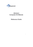
CM-X300 CoM
Reference Guide Rev 1.31
12/30/2010
© 2010 CompuLab Ltd.
All Rights Reserved. No part of this document may be photocopied, reproduced, stored in
a retrieval system, or transmitted, in any form or by any means whether, electronic,
mechanical, or otherwise without the prior written permission of CompuLab Ltd..
No warranty of accuracy is given concerning the contents of the information contained in
this publication. To the extent permitted by law no liability (including liability to any
person by reason of negligence) will be accepted by CompuLab Ltd., its subsidiaries or
employees for any direct or indirect loss or damage caused by omissions from or
inaccuracies in this document.
CompuLab Ltd. reserves the right to change details in this publication without notice.
Product and company names herein may be the trademarks of their respective owners.
CompuLab Ltd.
P.O.B. 66 Nesher
36770 ISRAEL
Tel: +972 (4) 8290100
http://www.compulab.co.il
Fax: +972 (4) 8325251
2
CM-X300 Reference Guide Rev 1.31
30-Dec-2010
Table of Contents
Table of Contents
1
INTRODUCTION ................................................................................................. 9
1.1
1.2
1.3
1.4
2
OVERVIEW ........................................................................................................ 10
2.1
2.2
3
About This Document ........................................................................................ 9
CM-X300 Part Number Legend ......................................................................... 9
Terminology ....................................................................................................... 9
Related Documents ............................................................................................. 9
Block Diagram .................................................................................................. 10
CM-X300 Features ........................................................................................... 11
FUNCTIONAL DESCRIPTION ....................................................................... 13
3.1 Board Layout .................................................................................................... 13
3.1.1 Top Side Components ............................................................................. 13
3.1.2 Bottom Side Components ........................................................................ 13
3.2 Connectors Pinout............................................................................................. 14
3.2.1 Interface Connectors ................................................................................ 14
3.2.1.1 Connector A ....................................................................................... 14
3.2.1.2 Connector B ....................................................................................... 17
3.3 Application Information ................................................................................... 20
3.3.1 Debug LED (DS1) ................................................................................... 20
3.3.2 Wireless LAN .......................................................................................... 20
3.3.2.1 Wireless LAN Specifications ............................................................ 21
3.3.2.2 WLAN Antenna Configuration ......................................................... 21
3.3.3 Bluetooth ................................................................................................. 21
3.3.3.1 Wireless LAN Specifications ............................................................ 22
3.3.3.2 Bluetooth Antenna Configuration ..................................................... 22
3.3.4 LAN Port ................................................................................................. 22
3.3.4.1 Accessing DM9000A ........................................................................ 23
3.3.4.2 Implementing Magnetics ................................................................... 23
3.3.5 Serial Ports............................................................................................... 24
3.3.5.1 Full-Function UART ......................................................................... 25
3.3.5.2 Console UART .................................................................................. 25
3.3.5.3 Partial-Function UART ..................................................................... 26
3.3.6 Local Bus ................................................................................................. 26
3.3.6.1 Local Bus Signal Description ............................................................ 26
3.3.6.2 Static Memory Controller Address Map ........................................... 27
3.3.6.3 Local Bus Operation .......................................................................... 27
3.3.7 Keypad ..................................................................................................... 27
3.3.8 LCD Interface .......................................................................................... 28
3.3.8.1 Limitations of Display Controller Capabilities ................................. 29
3.3.9 USB ......................................................................................................... 31
3.3.9.1 USB Controllers ................................................................................ 31
30-Dec-2010
CM-X300 Reference Guide Rev 1.31
3
CM-X300 CoM
3.3.9.2 USB Interfaces Routing ..................................................................... 32
3.3.9.3 USB1 Interface ................................................................................... 32
3.3.9.4 USB2 Interface ................................................................................... 32
3.3.9.5 USB3 Interface ................................................................................... 32
3.3.10
MMC/SD/SDIO Controller .................................................................. 33
3.3.10.1 MMC/SD/SDIO Controller Features ............................................... 33
3.3.10.2 MMC/SD/SDIO Controller Interface Signals .................................. 33
3.3.11
GPIO ..................................................................................................... 34
3.3.11.1 I2C Operated GPIOs ......................................................................... 34
3.3.11.2 CPU GPIO........................................................................................ 34
3.3.12
Camera Interface................................................................................... 37
3.3.13
Audio Subsystem .................................................................................. 38
3.3.13.1 Audio I/O ......................................................................................... 38
3.3.13.2 AC‘97 Bus........................................................................................ 38
3.3.14
Touch Panel Interface ........................................................................... 38
3.3.15
Power .................................................................................................... 39
3.3.16
System Signals ...................................................................................... 39
3.3.17
I2C Bus .................................................................................................. 40
3.3.18
Synchronous Serial Port (SSP) ............................................................. 40
3.3.18.1 SSP Features .................................................................................... 41
3.3.18.2 Turning the SSP Port On .................................................................. 41
3.3.19
PWM Controller ................................................................................... 41
3.3.19.1 PWM Features.................................................................................. 42
3.3.19.2 PWM Operation ............................................................................... 42
3.3.19.3 PWM Reset Sequence ...................................................................... 43
3.3.19.4 Programming Considerations ........................................................... 43
3.3.19.5 PWM Register Summary ................................................................. 44
3.3.19.6 PWM Control Register (PWMCRx) ................................................ 45
3.3.19.7 PWM Duty Cycle Register (PWMDCRx) ....................................... 45
3.3.19.8 PWM Period Control Register (PWMPCRx) .................................. 45
4
BASEBOARD INTERFACE .............................................................................. 47
4.1 CAMI Connectors ............................................................................................. 47
4.1.1 Connectors Type and Layout ................................................................... 47
4.1.2 Standoffs .................................................................................................. 47
4.2 Mechanical drawings ........................................................................................ 48
4.3 Baseboard Design Guidelines ........................................................................... 49
4.4 Baseboard Troubleshooting .............................................................................. 49
5
OPERATING TEMPERATURE RANGES ..................................................... 51
6
POWER CONSUMPTION ................................................................................. 52
4
CM-X300 Reference Guide Rev 1.31
30-Dec-2010
Table of Contents
List of Figures
Figure 1
Figure 2
Figure 3
Figure 4
Figure 5
Figure 6
Figure 7
Figure 8
Figure 9
Figure 10
Figure 11
30-Dec-2010
CM-X300 Block Diagram............................................................................ 10
CM-X300 Top View Diagram ..................................................................... 13
CM-X300 Bottom View Diagram ............................................................... 14
Magnetic Interconnect Schematic ................................................................ 24
DC Source for Magnetic Center Taps .......................................................... 24
PXA300 Processor Block Diagram ............................................................. 29
PWM Block Diagram .................................................................................. 42
Basic PWM Waveform ................................................................................ 42
Effect of PWMCR2 Settings ........................................................................ 43
CM-X300 Top View ................................................................................... 48
CM-X300 Bottom (X-Ray view – as aeen from the top side) .................... 48
CM-X300 Reference Guide Rev 1.31
5
CM-X300 CoM
List of Tables
Table 1
Table 2
Table 3
Table 4
Table 5
Table 6
Table 7
Table 8
Table 9
Table 10
Table 11
Table 12
Table 13
Table 14
Table 15
Table 16
Table 17
Table 18
Table 19
Table 20
Table 21
Table 22
Table 23
Table 24
Table 25
Table 26
Table 27
Table 28
Table 29
Table 30
Table 31
Table 32
Table 33
Table 34
Table 35
Table 36
Table 37
Table 38
Table 39
Table 40
Table 41
Table 42
6
Acronyms ....................................................................................................... 9
Related Documents......................................................................................... 9
CPU, Memory and Busses............................................................................ 11
Peripherals .................................................................................................... 11
Electrical, Mechanical and Environmental Specifications ........................... 12
Top Side Components .................................................................................. 13
Bottom Side Components ............................................................................. 14
Connector A (P1) pinout .............................................................................. 14
Connector B (P2) pinout............................................................................... 17
802.11b RF System Specifications ............................................................... 21
802.11g RF System Specifications ............................................................... 21
Bluetooth RF System Specifications ............................................................ 22
LAN port signals .......................................................................................... 22
Recommended Magnetic Modules ............................................................... 23
Full-Function UART Signals ....................................................................... 25
Console UART Signals ................................................................................ 25
Partial-Function UART Signals ................................................................... 26
Local Bus Signals (SMC) ............................................................................. 26
Local Bus Signals (NFC) ............................................................................. 27
SMC Address Map ....................................................................................... 27
Keypad Signals ............................................................................................. 28
LCD Signals ................................................................................................. 29
USB Interfaces ............................................................................................. 32
USB1 CAMI Port Signals ............................................................................ 32
USB2 CAMI Port Signals ............................................................................ 32
USB3 CAMI Port Signals ............................................................................ 33
MMC and SD/SDIO Mode Signals .............................................................. 33
SPI Mode Signals ......................................................................................... 34
GPIO Extenders ............................................................................................ 34
I2C Operated GPIO Signals .......................................................................... 34
I2C Operated GPIO DC Characteristics ....................................................... 34
CPU GPIO Signals ....................................................................................... 35
CPU GPIO Registers .................................................................................... 35
CPU GPIO DC Characteristics..................................................................... 37
Camera Interface Signals .............................................................................. 37
Audio I/O Signals ......................................................................................... 38
AC‘97 Bus Signals ....................................................................................... 38
Touch Panel Interface Signals ...................................................................... 39
Power Signals ............................................................................................... 39
Battery and Charger Operating Conditions .................................................. 39
System Signals ............................................................................................. 40
I2C Signals .................................................................................................... 40
CM-X300 Reference Guide Rev 1.31
30-Dec-2010
List of Tables
Table 43
Table 44
Table 45
Table 46
Table 47
Table 48
Table 49
Table 50
Table 51
Table 52
Table 53
Table 54
30-Dec-2010
SSP1 Port Signals ........................................................................................ 40
SSP3 Port Signals ........................................................................................ 40
PWM Signals ............................................................................................... 41
PWM Registers ............................................................................................ 44
PWM Control Register ................................................................................ 45
PWM Duty Cycle Register .......................................................................... 45
PWM Period Control Register ..................................................................... 46
CAMI Connectors ........................................................................................ 47
Standoff Part List ......................................................................................... 47
CM-X300 Temperature Range Options ....................................................... 51
CM-X300 Power Consumption (BT and Wi-Fi enabled) ............................ 52
CM-X300 Power Consumption (BT and Wi-Fi disabled) ........................... 52
CM-X300 Reference Guide Rev 1.31
7
CM-X300 CoM
Revision Information
Date
Description
September 01, 2008
October 29, 2008
November 30, 2008
December 01, 2008
December 14, 2008
March 17, 2009
Preliminary release
CM-X300 rev 1.1 release
Added section 3.3.19, PWM Controller.
Added section 3.3.8.1, Limitations of Display Controller Capabilities.
Added section 3.3.4.2, Implementing Magnetics
CM-X300 Revision 1.2 introduced
Block Diagram (Figure 1) updated
Section 2.2 CM-X300 Features updated
Section 3.3.8.1 Limitations of Display Controller Capabilities updated
with the PXA300 block diagram
Section 3.3.18 Synchronous Serial Port (SSP) updated: SSP3 port added.
Antenna disconnection instructions added to the sections 3.3.2 Wireless
LAN and 3.3.3 Bluetooth
Section 3.3.7 Keypad updated.
Note about LB-CS0 usage added
CAMI connectors pin functions updated (keypad)
Active power consumption data updated in the features table (1.5W max)
Standby power consumption data updated in the features table (50mW)
Added the chapter 6, Power Consumption, on page 52
PWM1 output added.
GPIO pins DC characteristics added
Formatting errors fixed
CIF GPIO info added
USB chapter revised
Standoff info updated
Note about CIF availability added
GPIO80..82 usage note added
FFUART availability on C624M note added
PWM1-OUT/GPIO18 pull-up/down note added
USB2 port functionality in C624M configuration updated
GPIO availability table updated
Battery option ―B‖ added to table 4
Updated tables 5, 39 and 40.
Updated chapter 3.3.15
June 16, 2009
October 12, 2009
November 15, 2009
November 22, 2009
December 20, 2009
February 02, 2010
February 16, 2010
March 02, 2010
May 26, 2010
Dec 20, 2010
Please check for a newer revision of this manual at CompuLab's web site –
http://www.compulab.co.il/. Compare the revision notes of the updated manual from the web site
with those of the printed or electronic form version you have.
8
CM-X300 Reference Guide Rev 1.31
30-Dec-2010
Introduction
1 INTRODUCTION
1.1 About This Document
This document is part of a set of reference documents providing information necessary to
operate and program CompuLab‘s CM-X300 Embedded PC Module, which are listed under
Related Documents in this section.
Additional chapters are as follows:
2. Overview
3. Functional Description
1.2 CM-X300 Part Number Legend
Please refer to the CompuLab Website‘s prices section for information about decoding the
CM-X300 part number: http://compulab.co.il/x300/html/x300-cm-price.htm.
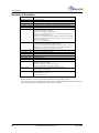
1.3 Terminology
Table 1
Acronyms
Term
CAMI
CoM
Description
CompuLab's Aggregated Module Interface. A standardized module connector interface
allowing interchangeability with other CM brand modules.
Computer-on-Modules are full-featured single board computers designed for mezzanine
attachment to custom application through miniature high-density connectors
1.4 Related Documents
For additional information not covered in this manual, refer to the documents listed in
Table 2.
Table 2
Related Documents
Document
X300 Products Developer Resources
Universal Serial Bus Specification, Revision 2.0
On-The-Go Supplement to Universal Serial Bus
Specification, Revision 2.0
Pullup/Pulldown Resistors Engineering Change
Notice to the USB 2.0 Specification
MultiMediaCard System Specification Version
3.3.1
SD Memory Card Specification Version 1.10
SDIO Card Specification Version 1.0
30-Dec-2010
Location
http://compulab.co.il/x300/html/x300-developer.py
CM-X300 Reference Guide Rev 1.31
9
CM-X300 CoM
2 OVERVIEW
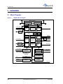
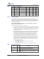
2.1 Block Diagram
Figure 1
CM-X300 Block Diagram
WiFi / BT module
Bluetooth (BC-4)
USB 1 (Host)
USB 2 (Host/Slave)
WiFi (88W8686)
Video
Acceleration
USB
MMC/SDIO
USB3 (Slave)
USB 2.0
XCVR
PXA300/310 MPU, 208 / 624 MHz
CPU
LCD Interface
GPIO x 32
(I2C I/F)
3.3 Volt Supply
WMMX
MMU
I-cache
D-cache
Graphics
Controller
DMA
Timers
Interrupts
Video Input
I2C Ctrl
Memory
Controller
AC97
Interface
PMIC
Charger &
Power Supply
Battery Supply &
Charge (optional)
RS232
Audio
Touchscreen
100BaseT
LEDs
RTC
Ethernet port
DM9000A
COM-A
AC97 link
Spkr & Mic
Resistive TS
W9712L
SYSTEM SUPPLY
VOLTAGES
BAT
COM-D
COM-C
Serial
Controller
DDR
64 - 128 MB
NAND Flash
(Bootable)
512 MB
Local Bus
10
CM-X300 Reference Guide Rev 1.31
30-Dec-2010
Overview
2.2
CM-X300 Features
The "Option" column specifies the configuration code required to have the particular
feature.
"+" means that the feature is always available.
Table 3
CPU, Memory and Busses
Feature
CPU
RAM
NAND Flash
Disk
External local
bus
AC97 bus
Table 4
Intel XScale PXA300/310, 208 / 624 MHz, WMMX2,
2*128K internal SRAM
32 KB I-cache and 32 KB D-cache, WB, 128 MB address
space
DMA and Interrupt controllers, Timers
64 - 128 MB, DDR, 208 MHz, 16-bit
512 Mbytes, bootable.
16-bit, variable rate up to 52 MHz, 3.3V tolerance
AC97 / AMC97 Rev 2.1 compliant
Option
C
D
N
+
+
Peripherals
Feature
Graphics
Controller
Hardware
accelleration
Video Input
Port
USB
Serial Ports
(UARTs)
Synchronous
Serial Port
(SSP)
Specifications
8/16 bit color, TFT / STN, frame buffer in CPU SRAM or
system DDR
Resolution: up to 800 x 480 x 16 without restrictions, and
up to 1024 x 1024 with some restrictions about overlays,
BPP and pixel clock.
Supports up to D1 decode and encode performance for
codecs including H.264, MPEG-4, H.263, MPEG-2,
RealVideo and Microsoft WMV9.
Hardware scaling, rotation and other raster graphics
operations.
* Implemented by selecting PXA310 CPU option
Direct camera sensor support, max resolution 2560 x
2048, pixel clock up to 52MHz
Host/Slave (OTG) port, 12 Mbps, 23-endpoints (in slave
mode), OHCI v1.0
Host port (shared with Bluetooth, therefore not available
with "W" option)
USB 2.0 HS client port
Up to 3 UART ports, 16550 compatible, max 921 kbps
COM-A - RS232, Rx / Tx
COM-C - TTL, full modem controls
COM-D - TTL, partial modem controls
One SSP port, 13mbps, supports SSP, SPI, I2S protocols.
Option
+
C624M
+
+
W
+
+
+
+
+
General
Purpose I/O
42 dedicated lines (32 I2C-controlled + 10 memorymapped) plus additional lines shared with other functions.
Can also be used as interrupt inputs.
+
Keyboard &
mouse
USB, keypad or redirection from COM port
+
Ethernet
Audio codec
Touchscreen
ctrl.
RTC
30-Dec-2010
Specifications
Davicom DM9000A MAC & PHY, 10/100BaseT,
Activity LED's
Wolfson W9712L, AC97 interface, mono microphone
input, stereo line input and 25 mW output for active
speakers
A part of the W9712L codec chip. Supports resistive
touch panels.
Real Time Clock, powered by external lithium battery
CM-X300 Reference Guide Rev 1.31
E
AT
AT
+
11
CM-X300 CoM
WiFi
Interface
Bluetooth
Battery
support
Implements 802.11b/g wireless connectivity standard
Supports Node to Access Point and Multi-Node (w/o
access point) methods of connection. (Cannot act as
Access Point)
Marvell 88W8686 802.11b/g chipset.
On-board ceramic chip antenna and connector for external
antenna.
Bluetooth V2.0+EDR system. CSR BlueCore4-ROM
chipset, 2.4GHz band, up to 3Mbps. On-board ceramic
chip antenna and connector for external antenna.
Bluetooth and WiFi interface are always assembled
together, and therefore are specified by the same
assembling option.
No battery support – operating voltage is 3.3V + 10% / 3%. Board is assembled with PMIC suitable for the
specified operating voltage range.
Battery support – operating range is 3.4V to 4.5V. Board
is assembled with PMIC dedicated for battery operation.
Table 5
W
+
B
Electrical, Mechanical and Environmental Specifications
Supply Voltage
Active power
consumption
Standby/Sleep
consumption
Dimensions
Weight
MTBF
Operation temperature
(case)
Storage temperature
Relative humidity
Shock
Vibration
Connectors
Connector insertion /
removal
12
W
Without ―B‖ option - 3.3V +10% / -3%
With ―B‖ option -3.4 to 4.7V (from battery or external regulator)
0.18 – 1.5 W, depending on configuration and CPU speed
50 mW
66 x 44 x 7 mm
25 gram
> 100,000 hours
Commercial: 0º to 70º C
Extended: -20º to 70º C
Industrial: -40º to 85º C
-40º to 85º C
10% to 90% (operation)
05% to 95% (storage)
50G / 20 ms
20G / 0 - 600 Hz
2 x 140 pin, 0.6 mm
50 cycles
CM-X300 Reference Guide Rev 1.31
30-Dec-2010
Functional Description
3
FUNCTIONAL DESCRIPTION
3.1 Board Layout
3.1.1 Top Side Components
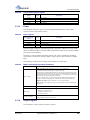
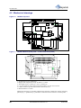
Figure 2 shows top side of CM-X300. The relevant top side components are listed in
Table 6.
Figure 2
CM-X300 Top View Diagram
R34
Q2
Q1
U19
U13
U1
X5
U2
ANT2
X4
J3
U3
L6
L7
DS1
U23
J1
Table 6
ANT1
Top Side Components
Reference
J1
J3
ANT1
ANT2
DS1
Function
Bluetooth external antenna connector
Wi-Fi external antenna connector
Bluetooth antenna
Wi-Fi antenna
Debug LED
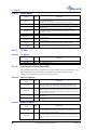
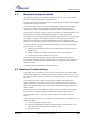
3.1.2 Bottom Side Components
Figure 3 shows bottom side of CM-X300. The bottom side components are listed in
Table 7.
30-Dec-2010
CM-X300 Reference Guide Rev 1.31
13
CM-X300 CoM
Figure 3
CM-X300 Bottom View Diagram
Table 7
Bottom Side Components
Reference
Function
P1
P2
CAMI connector A
CAMI connector B
3.2 Connectors Pinout
3.2.1 Interface Connectors
CAMI signal names, as described in the CAMI Specification as of February 4, 2004, are
listed in the tables below. Signal descriptions may be found in the CM-X072 User‘s
Manual. CAMI names are provided for easy comparison with previous modules.
3.2.1.1
Connector A
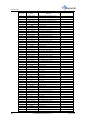
Table 8
Connector A (P1) pinout
Conn-Pin
P1-01
P1-02
P1-03
P1-04
P1-05
P1-06
P1-07
P1-08
P1-09
P1-10
P1-11
P1-12
P1-13
P1-14
P1-15
14
CM-X300 Signal
Name
ETH1-TDP
ETH1-RDN
ETH1-TDN
ETH1-RDP
ETH1-SPEED#
ETH1-LINK-ACT#
VCHRG
GND
WP1#
N.C.
RST-IN#
N.C.
KP_MKOUT0
GPIO121
GND
KP_MKOUT2
GPIO123
Reference
LAN Port, page 22
LAN Port, page 22
LAN Port, page 22
LAN Port, page 22
LAN Port, page 22
LAN Port, page 22
Power, page 39
Power, page 39
System Signals, page 39
No Connect
System Signals, page 39
No Connect
Keypad, page 27
CPU GPIO, page 34
Power, page 39
Keypad, page 27
CPU GPIO, page 34
CM-X300 Reference Guide Rev 1.31
CAMI Signal Name
ETH1-TDP
ETH1-RDN
ETH1-TDN
ETH1-RDP
ETH1-LINK100#
ETH1-LINK10#
VCORE
GND
WP1#
ETH1-ACT#
RST-IN#
SPARE
GPIO0
GND
GPIO2
30-Dec-2010
Functional Description
Conn-Pin
P1-16
P1-17
P1-18
P1-19
P1-20
P1-21
P1-22
P1-23
P1-24
P1-25
P1-26
P1-27
P1-28
P1-29
P1-30
P1-31
P1-32
P1-33
P1-34
P1-35
P1-36
P1-37
P1-38
P1-39
P1-40
P1-41
P1-42
P1-43
P1-44
P1-45
P1-46
P1-47
P1-48
P1-49
P1-50
P1-51
P1-52
P1-53
P1-54
P1-55
P1-56
P1-57
P1-58
P1-59
30-Dec-2010
CM-X300 Signal
Name
KP_MKOUT1
GPOP122
EXTWAKE#
KP_MKOUT3
GPIO124
VCHRG
VCC-RTC
ONKEY#
COM-A-RX#
N.C.
COM-A-TX#
N.C.
GND
COM-D-RX
GPIO112
COM-C-RX
GPIO30
COM-D-TX
GPIO113
COM-C-TX
GPIO31
VBAT
COM-C-DCD#
GPIO33
N.C.
COM-C-DTR#
GPIO36
N.C.
COM-C-DSR#
GPIO34
N.C.
GND
COM-D-CTS#
GPIO114
COM-C-CTS#
GPIO32
COM-D-RTS#
GPIO111
COM-C-RTS#
GPIO37
VCHRG
COM-C-RIN#
GPIO35
N.C.
DF_CLE_nOE
LB-CS0#
DF_ALE_nWE
PWM2-OUT
GPIO19
GND
PWM1-OUT
GPIO18
LB-CS1#
TS-XP
N.C.
VCHRG
BOOTENA#
TS-YP
N.C.
N.C.
Reference
Keypad, page 27
CPU GPIO, page 34
System Signals, page 39
Keypad, page 27
CPU GPIO, page 34
Power, page 39
Power, page 39
System Signals, page 39
Console UART, page 25
No Connect
Console UART, page 25
No Connect
Power, page 39
Partial-Function UART, page 26
CPU GPIO, page 34
Full-Function UART, page 25
CPU GPIO, page 34
Partial-Function UART, page 26
CPU GPIO, page 34
Full-Function UART, page 25
CPU GPIO, page 34
Power, page 39
Full-Function UART, page 25
CPU GPIO, page 34
No Connect
Full-Function UART, page 25
CPU GPIO, page 34
No Connect
Full-Function UART, page 25
CPU GPIO, page 34
No Connect
Power, page 39
Partial-Function UART, page 26
CPU GPIO, page 34
Full-Function UART, page 25
CPU GPIO, page 34
Partial-Function UART, page 26
CPU GPIO, page 34
Full-Function UART, page 25
CPU GPIO, page 34
Power, page 39
Full-Function UART, page 25
CPU GPIO, page 34
No Connect
Local Bus, page 26
Local Bus, page 26
Local Bus, page 26
PWM Controller, page 41
CPU GPIO, page 34
Power, page 39
PWM Controller, page 41
CPU GPIO, page 34
Local Bus, page 26
Touch Panel Interface, page 38
No Connect
Power, page 39
System Signals, page 39
Touch Panel Interface, page 38
No Connect
No Connect
CM-X300 Reference Guide Rev 1.31
CAMI Signal Name
GPIO1
PME#
GPIO3
VCORE
VCC-RTC
SUSP-IN
COM-A-RX
COM-B-RX
COM-A-TX
COM-B-TX
GND
COM-D-RX
COM-C-RX
COM-D-TX
COM-C-TX
VCC3-3
COM-C-DCD#
COM-D-DCD#
COM-C-DTR#
COM-D-DTR#
COM-C-DSR#
COM-D-DSR#
GND
COM-D-CTS#
COM-C-CTS#
COM-D-RTS#
COM-C-RTS#
VCORE
COM-C-RIN#
COM-D-RIN#
IDE-RD#
IDE-CS0#
IDE-WR#
IDE-IRQ
GND
LB-IRQ0
LB/IDE-CS1#
TS-XP
LB-IRQ1
VCORE
DEBUG1
TS-YP
DEBUG0
SSI-DIN
15
CM-X300 CoM
Conn-Pin
P1-60
P1-61
P1-62
P1-63
P1-64
P1-65
P1-66
P1-67
P1-68
P1-69
P1-70
P1-71
P1-72
P1-73
P1-74
P1-75
P1-76
P1-77
P1-78
P1-79
P1-80
P1-81
P1-82
P1-83
P1-84
P1-85
P1-86
P1-87
P1-88
P1-89
P1-90
P1-91
P1-92
P1-93
P1-94
P1-95
P1-96
P1-97
P1-98
P1-99
P1-100
P1-101
P1-102
P1-103
P1-104
P1-105
P1-106
P1-107
P1-108
P1-109
P1-110
16
CM-X300 Signal
Name
I2C-DATA
I2C-CLK
GND
DF-A1
DF-A0
DF-A3
DF-A2
VBAT
N.C.
GPIO80
DF-CS0#
GPIO81
DF-CS1#
GPIO82
GND
GPIO83
LB-RDY
GPIO84
LB-BE0#
VCHRG
LB-BE1#
GPIO85/
SSPSCLK/
KP_DKIN0
LB-LLA#
GPIO86/
SSPSFRM/
KP_DKIN1
LB-LUA#
GPIO87/
SSPTXD/
KP_DKIN2
GND
GPIO88/
SSPTXD/
KP_DKIN3
DF-RB#
GPIO89
DF-RE#
VCHRG
DF-WE#
GPIO90
DF-IO0
DF-IO1
DF-IO2
DF-IO3
GND
DF-IO5
DF-IO4
DF-IO7
DF-IO6
VBAT
DF-IO8
DF-IO9
DF-IO10
DF-IO11
DF-IO12
DF-IO13
GND
Reference
I2C Bus, page 40
I2C Bus, page 40
Power, page 39
Local Bus, page 26
Local Bus, page 26
Local Bus, page 26
Local Bus, page 26
Power, page 39
No Connect
CPU GPIO, page 34 (C624 only)
Local Bus, page 26
CPU GPIO, page 34 (C624 only)
Local Bus, page 26
CPU GPIO, page 34 (C624 only)
Power, page 39
CPU GPIO, page 34
Local Bus, page 26
CPU GPIO, page 34
Local Bus, page 26
Power, page 39
Local Bus, page 26
CPU GPIO, page 34
Synchronous Serial Port (SSP), page 40
Keypad, page 27
Local Bus, page 26
CPU GPIO, page 34
Synchronous Serial Port (SSP), page 40
Keypad, page 27
Local Bus, page 26
CPU GPIO, page 34
Synchronous Serial Port (SSP), page 40
Keypad, page 27
Power, page 39
CPU GPIO, page 34
Synchronous Serial Port (SSP), page 40
Keypad, page 27
Local Bus, page 26
CPU GPIO, page 34
Local Bus, page 26
Power, page 39
Local Bus, page 26
CPU GPIO, page 34
Local Bus, page 26
Local Bus, page 26
Local Bus, page 26
Local Bus, page 26
Power, page 39
Local Bus, page 26
Local Bus, page 26
Local Bus, page 26
Local Bus, page 26
Power, page 39
Local Bus, page 26
Local Bus, page 26
Local Bus, page 26
Local Bus, page 26
Local Bus, page 26
Local Bus, page 26
Power, page 39
CM-X300 Reference Guide Rev 1.31
CAMI Signal Name
SSI-DOUT
SSI-CLK
GND
LB-A1
LB-A0
LB-A3
LB-A2
VCC3-3
LB-A4
LB-A5
LB-A6
LB-A7
LB-A8
LB-A9
GND
LB-A11
LB-A10
LB-A13
LB-A12
VCORE
LB-A14
LB-A15
LB-A16
LB-A17
LB-A18
LB-A19
GND
LB-A21
LB-A20
LB-A23
LB-A22
VCORE
LB-A24
LB-A25
LB-D0
LB-D1
LB-D2
LB-D3
GND
LB-D5
LB-D4
LB-D7
LB-D6
VCC3-3
LB-D8
LB-D9
LB-D10
LB-D11
LB-D12
LB-D13
GND
30-Dec-2010
Functional Description
Conn-Pin
P1-111
P1-112
P1-113
P1-114
P1-115
P1-116
P1-117
P1-118
P1-119
P1-120
P1-121
P1-122
P1-123
P1-124
P1-125
P1-126
P1-127
P1-128
P1-129
P1-130
P1-131
P1-132
P1-133
P1-134
P1-135
P1-136
P1-137
P1-138
P1-139
P1-140
CM-X300 Signal
Name
DF-IO15
DF-IO14
N.C.
N.C.
VCHRG
N.C.
N.C.
N.C.
N.C.
N.C.
N.C.
GND
KP_MKIN4
GPIO119
KP_MKIN3
GPIO118
KP_MKOUT5
GPIO4_2
KP_MKOUT4
GPIO125
VCHRG
KP_MKIN0
GPIO115
KP_MKIN6
GPIO2_2
KP_MKIN5
GPIO120
N.C.
KP_MKIN7
GPIO3_2
LB-CS2#
GND
LB-CS3#
nXCVREN
USBD-P
RST-OUT#
USBD-N
VBAT
N.C.
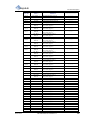
3.2.1.2
Connector B
Table 9
Connector B (P2) pinout
30-Dec-2010
Conn-Pin
CM-X300 Signal
Name
P2-01
P2-02
P2-03
P2-04
P2-05
P2-06
P2-07
P2-08
P2-09
P2-10
P2-11
P2-12
N.C.
GND
N.C.
EXT_TBAT
N.C.
N.C.
VBAT
N.C.
MMC_DAT1
MMC_DAT0
MMC_DAT3
MMC_DAT2
Reference
Local Bus, page 26
Local Bus, page 26
No Connect
No Connect
Power, page 39
No Connect
No Connect
No Connect
No Connect
No Connect
No Connect
Power, page 39
Keypad, page 27
CPU GPIO, page 34
Keypad, page 27
CPU GPIO, page 34
Keypad, page 27
CPU GPIO, page 34
Keypad, page 27
CPU GPIO, page 34
Power, page 39
Keypad, page 27
CPU GPIO, page 34
Keypad, page 27
CPU GPIO, page 34
Keypad, page 27
CPU GPIO, page 34
No Connect
Keypad, page 27
CPU GPIO, page 34
Local Bus, page 26
Power, page 39
Local Bus, page 26
USB3 Interface, page 32
System Signals, page 39
USB3 Interface, page 32
Power, page 39
No Connect
Reference
No Connect
Power, page 39
No Connect
System Signals, page 39
No Connect
No Connect
Power, page 39
No Connect
MMC/SD/SDIO Controller, page 33
MMC/SD/SDIO Controller, page 33
MMC/SD/SDIO Controller, page 33
MMC/SD/SDIO Controller, page 33
CM-X300 Reference Guide Rev 1.31
CAMI Signal Name
LB-D15
LB-D14
LB-IORDY
LB-IOCS16#
VCORE
LB-RD#
PCM-MEMR#
LB-WR#
PCM-IOR#
PCM-MEMW#
PCM-IOW#
GND
PCM-WAIT#
PCM-CE1#
PCM-RST#
PCM-CDA#
VCORE
PCM-INTRDYA
PCM-REG#
PCM-WE#
PCM-CE2#
PCM-SKTSEL
LB-CS0#
GND
LB-CS1#
USB3-P
RST-OUT#
USB3-N
VCC3-3
VCC5
CAMI Signal Name
PCI-REQ0#
GND
PCI-GNT0#
SPARE
PCI-GNT1#
PCI-INTA#
VCC3-3
PCI-INTB#
LPC-LAD1
LPC-LAD0
LPC-LAD3
LPC-LAD2
17
CM-X300 CoM
18
Conn-Pin
CM-X300 Signal
Name
P2-13
P2-14
P2-15
P2-16
P2-17
P2-18
P2-19
P2-20
P2-21
P2-22
P2-23
P2-24
P2-25
P2-26
P2-27
P2-28
P2-29
P2-30
P2-31
P2-32
P2-33
P2-34
P2-35
P2-36
P2-37
P2-38
P2-39
P2-40
P2-41
P2-42
P2-43
P2-44
P2-45
P2-46
P2-47
P2-48
P2-49
P2-50
P2-51
P2-52
P2-53
P2-54
P2-55
P2-56
P2-57
P2-58
P2-59
P2-60
P2-61
P2-62
P2-63
P2-64
P2-65
P2-66
P2-67
P2-68
P2-69
MMC_CMD1
GND
MMC_CMD0
MMC_CLK
N.C.
N.C.
VCHRG
I2C_GPIO0_0
I2C_GPIO0_2
I2C_GPIO0_1
I2C_GPIO0_4
I2C_GPIO0_3
I2C_GPIO0_5
GND
I2C_GPIO0_7
I2C_GPIO0_6
I2C_GPIO1_0
N.C.
VCHRG
I2C_GPIO1_1
I2C_GPIO1_3
I2C_GPIO1_2
I2C_GPIO1_5
I2C_GPIO1_4
I2C_GPIO1_6
GND
N.C.
I2C_GPIO1_7
N.C.
N.C.
VBAT
N.C.
N.C.
N.C.
N.C.
N.C.
N.C.
GND
I2C_GPIO2_0
N.C.
I2C_GPIO2_2
I2C_GPIO2_1
VCHRG
I2C_GPIO2_3
I2C_GPIO2_5
I2C_GPIO2_4
I2C_GPIO2_7
I2C_GPIO2_6
N.C.
GND
I2C_GPIO3_1
I2C_GPIO3_0
I2C_GPIO3_3
I2C_GPIO3_2
VCHRG
I2C_GPIO3_4
I2C_GPIO3_6
Reference
MMC/SD/SDIO Controller, page 33
Power, page 39
MMC/SD/SDIO Controller, page 33
MMC/SD/SDIO Controller, page 33
No Connect
No Connect
Power, page 39
I2C Operated GPIO, page 34
I2C Operated GPIO, page 34
I2C Operated GPIO, page 34
I2C Operated GPIO, page 34
I2C Operated GPIO, page 34
I2C Operated GPIO, page 34
Power, page 39
I2C Operated GPIO, page 34
I2C Operated GPIO, page 34
I2C Operated GPIO, page 34
No Connect
Power, page 39
I2C Operated GPIO, page 34
I2C Operated GPIO, page 34
I2C Operated GPIO, page 34
I2C Operated GPIO, page 34
I2C Operated GPIO, page 34
I2C Operated GPIO, page 34
Power, page 39
No Connect
I2C Operated GPIO, page 34
No Connect
No Connect
Power, page 39
No Connect
No Connect
No Connect
No Connect
No Connect
No Connect
Power, page 39
I2C Operated GPIO, page 34
No Connect
I2C Operated GPIO, page 34
I2C Operated GPIO, page 34
Power, page 39
I2C Operated GPIO, page 34
I2C Operated GPIO, page 34
I2C Operated GPIO, page 34
I2C Operated GPIO, page 34
I2C Operated GPIO, page 34
No Connect
Power, page 39
I2C Operated GPIO, page 34
I2C Operated GPIO, page 34
I2C Operated GPIO, page 34
I2C Operated GPIO, page 34
Power, page 39
I2C Operated GPIO, page 34
I2C Operated GPIO, page 34
CM-X300 Reference Guide Rev 1.31
CAMI Signal Name
LPC-SERIRQ
GND
LPC-LFRAME#
PCI-CLK0
LPC-LDRQ#
PCI-REQ1#
VCORE
PCI-AD0
PCI-AD2
PCI-AD1
PCI-AD4
PCI-AD3
PCI-AD5
GND
PCI-AD7
PCI-AD6
PCI-AD8
PCI-CBE0#
VCORE
PCI-AD9
PCI-AD11
PCI-AD10
PCI-AD13
PCI-AD12
PCI-AD14
GND
PCI-CBE1#
PCI-AD15
PCI-SERR#
PCI-PAR
VCC3-3
PCI-PERR#
PCI-DEVSEL#
PCI-STOP#
PCI-IRDY#
PCI-TRDY#
PCI-FRAME#
GND
PCI-AD16
PCI-CBE2#
PCI-AD18
PCI-AD17
VCORE
PCI-AD19
PCI-AD21
PCI-AD20
PCI-AD23
PCI-AD22
PCI-CBE3#
GND
PCI-AD25
PCI-AD24
PCI-AD27
PCI-AD26
VCORE
PCI-AD28
PCI-AD30
30-Dec-2010
Functional Description
Conn-Pin
P2-70
P2-71
P2-72
P2-73
P2-74
P2-75
30-Dec-2010
CM-X300 Signal
Name
I2C_GPIO3_5
TS-XM
I2C_GPIO3_7
TS-YM
GND
CIF_DD2
GPIO41
P2-76
CIF_DD3
GPIO42
P2-77
CIF_DD1
GPIO40
P2-78
CIF_DD4
GPIO43
P2-79
VBAT
P2-80
CIF_DD5
GPIO44
P2-81
CIF_DD0
GPIO39
P2-82
CIF_DD6
GPIO45
P2-83
CIF_DD9
GPIO48
P2-84
CIF_DD7
GPIO46
P2-85
CIF_DD8
GPIO47
P2-86
GND
P2-87
CIF_FV
GPIO52
P2-88
CIF_MCLK
GPIO49
P2-89
SYS_EN
P2-90
CIF_LV
GPIO51
P2-91
P2-92
VCHRG
N.C.
P2-93
CIF_PCLK
GPIO50
P2-94
P2-95
P2-96
P2-97
P2-98
P2-99
P2-100
P2-101
P2-102
P2-103
P2-104
P2-105
P2-106
P2-107
P2-108
P2-109
P2-110
P2-111
P2-112
P2-113
N.C.
LCD-B1
LCD-LP
LCD-B2
GND
LCD-B4
LCD-B3
LCD-G0
LCD-B5
VCHRG
LCD-G1
LCD-G3
LCD-G2
LCD-G5
LCD-G4
LCD-R1
GND
LCD-FRM
LCD-SCK
LCD-R2
Reference
I2C Operated GPIO, page 34
Touch Panel Interface, page 38
I2C Operated GPIO, page 34
Touch Panel Interface, page 38
Power, page 39
Camera Interface, page 37
CPU GPIO, page 34
Camera Interface, page 37
CPU GPIO, page 34
Camera Interface, page 37
CPU GPIO, page 34
Camera Interface, page 37
CPU GPIO, page 34
Power, page 39
Camera Interface, page 37
CPU GPIO, page 34
Camera Interface, page 37
CPU GPIO, page 34
Camera Interface, page 37
CPU GPIO, page 34
Camera Interface, page 37
CPU GPIO, page 34
Camera Interface, page 37
CPU GPIO, page 34
Camera Interface, page 37
CPU GPIO, page 34
Power, page 39
Camera Interface, page 37
CPU GPIO, page 34
Camera Interface, page 37
CPU GPIO, page 34
System Signals, page 39
Camera Interface, page 37
CPU GPIO, page 34
Power, page 39
No Connect
Camera Interface, page 37
CPU GPIO, page 34
No Connect
LCD Interface, page 28
LCD Interface, page 28
LCD Interface, page 28
Power, page 39
LCD Interface, page 28
LCD Interface, page 28
LCD Interface, page 28
LCD Interface, page 28
Power, page 39
LCD Interface, page 28
LCD Interface, page 28
LCD Interface, page 28
LCD Interface, page 28
LCD Interface, page 28
LCD Interface, page 28
Power, page 39
LCD Interface, page 28
LCD Interface, page 28
LCD Interface, page 28
CM-X300 Reference Guide Rev 1.31
CAMI Signal Name
PCI-AD29
TS-XM
PCI-AD31
TS-YM
GND
PP-PD2
PP-PD3
PP-PD1
PP-PD4
VCC3-3
PP-PD5
PP-PD0
PP-PD6
PP-STROBE#
PP-PD7
PP-ALF#
GND
PP-ERROR#
PP-ACK#
PP-INIT#
PP-BUSY
VCORE
PP-PE
PP-SLCTIN#
PP-SLCT
LCD-B1
LCD-LP
LCD-B2
GND
LCD-B4
LCD-B3
LCD-G0
LCD-B5
VCORE
LCD-G1
LCD-G3
LCD-G2
LCD-G5
LCD-G4
LCD-R1
GND
LCD-FRM
LCD-SCK
LCD-R2
19
CM-X300 CoM
Conn-Pin
CM-X300 Signal
Name
P2-114
P2-115
P2-116
P2-117
P2-118
P2-119
P2-120
P2-121
P2-122
P2-123
LCD-DE
VCHRG
LCD-R3
LCD-R5
LCD-R4
N.C.
N.C.
SSPTXD3
GND
SSPRXD3
LCD Interface, page 28
Power, page 39
LCD Interface, page 28
LCD Interface, page 28
LCD Interface, page 28
No Connect
No Connect
Synchronous Serial Port (SSP), page 40
Power, page 39
Synchronous Serial Port (SSP), page 40
P2-124
SSPSFRM3
Synchronous Serial Port (SSP), page 40
P2-125
KP_MKIN2
GPIO117
Keypad, page 27
CPU GPIO, page 34
P2-126
SSPSCLK3
Synchronous Serial Port (SSP), page 40
P2-127
VCHRG
KP_MKIN1
GPIO116
AUD-SPDIF/
AC97_RST#
AUD-INR/
AC97_SDOUT
AUD-OUTL/
AC97_SDIN
AUD-INL-MIC/
AC97_BITCLK
USB-OTG-ID
GND
VBAT
AUD-OUTR/
AC97_SYNC
USB-OTG-P
USBH-P
USB-OTG-N
USBH-N
P2-128
P2-129
P2-130
P2-131
P2-132
P2-133
P2-134
P2-135
P2-136
P2-137
P2-138
P2-139
P2-140
Reference
Power, page 39
Keypad, page 27
CPU GPIO, page 34
Audio Subsystem, page 38
Audio Subsystem, page 38
Audio Subsystem, page 38
Audio Subsystem, page 38
USB2 Interface, page 32
Power, page 39
Power, page 39
Audio Subsystem, page 38
USB2 Interface, page 32
USB1 Interface, page 32
USB2 Interface, page 32
USB1 Interface, page 32
3.3
Application Information
3.3.1
Debug LED (DS1)
CAMI Signal Name
LCD-DE-M
VCORE
LCD-R3
LCD-R5
LCD-R4
PS2-KDAT
PS2-KCLK
IRDA-TX
GND
IRDA-RX
PS2-MDAT
[USB5-P]
PCM-CDB#
PS2-MCLK
[USB5-N]
VCORE
PCM-INTRDYB
AUD-SPDIF
[AC97-RST#]
AUD-INR
[AC97-SDOUT]
AUD-OUTL
[AC97-SDIN1]
AUD-INL-MIC
[AC97-BITCLK]
USB-OVC#
GND
VCC3-3
AUD-OUTR
[AC97-SYNC]
USB2-P
USB1-P
USB2-N
USB1-N
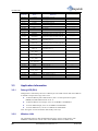
Debug LED is controlled by the CPU‘s GPIO79 pin. The LED will turn ON when GPIO79
is defined as output and its logic state is low.
To define GPIO79 pad‘s GPIO function, bits 0..2 of the pad control register
(MFPR) at 0x40E104D0 must be set to ‗0‘
To define GPIO79 as an output, set bit 15 of GPDR2 at 0x40E00014
To assert GPIO79 high, set bit 15 of GPSR2 at 0x40E00020
To assert GPIO79 low, set bit 15 of GPCR2 at 0x40E0002C
Note: all register accesses should be read-modify-write only!
3.3.2
Wireless LAN
The CM-X300 features a Marvell 88W8686 802.11b/g wireless LAN solution. The
88W8686 communicates with the CPU via the MMC2 interface in SDIO mode.
20
CM-X300 Reference Guide Rev 1.31
30-Dec-2010
Functional Description
3.3.2.1
Wireless LAN Specifications
The CM-X300‘s wireless LAN‘s 802.11b RF specifications are listed in Table 10; 802.11g
specs in Table 11.
Table 10
11.288b RF System Specifications
Parameter
Test Condition
Transmit Power Output
Maximum Receive Level
Transmit Frequency Offset
1 Mbps, 8% PER
2 Mbps, 8% PER
5.5 Mbps, 8% PER
11 Mbps, 8% PER
PER<8%
Low, Middle, High Channels
Spectral Mask
Max. TX Power
Error Vector Magnitude
Carrier Suppression
Max. TX Power @ 11Mbps
Max. TX Power
Desired channel is 3dB above
sensitivity, 11Mbps, PER<8%
Receive Sensitivity
Adjacent Channel Rejection
Table 11
Units
15
-90
-90
-90
-88
IEEE Compliant
±10
-40@fc±11MHz
-60@fc±22MHz
-36
-25
dBm
dBm
dBm
dBm
dBm
dBm
PPM
48
dBc
Typical Value
Units
15
-90
-88
-88
-87
-83
-80
-75
-74
IEEE Compliant
±10
-30@fc±11MHz
-40@fc±20MHz
-50@fc±30MHz
-29
-25
dBm
dBm
dBm
dBm
dBm
dBm
dBm
dBm
dBm
dBm
PPM
15
dBc
dBc
dB
dBc
11.288g RF System Specifications
Parameter
Test Condition
Transmit Power Output
Maximum Receive Level
Transmit Frequency Offset
6 Mbps, 10% PER
9 Mbps, 10% PER
12 Mbps, 10% PER
18 Mbps, 10% PER
24 Mbps, 10% PER
36 Mbps, 10% PER
48 Mbps, 10% PER
54 Mbps, 10% PER
PER<10%
Low, Middle, High Channels
Spectral Mask
Max. TX Power
Error Vector Magnitude
Carrier Suppression
Max. TX Power @ 11Mbps
Max. TX Power
Desired channel is 3dB above
sensitivity, 11Mbps, PER<8%
Receive Sensitivity
Adjacent Channel Rejection
3.3.2.2
Typical Value
dBc
dB
dBc
WLAN Antenna Configuration
The CM-X300 provides two possible WLAN antenna configurations. By default, an
onboard WLAN antenna ANT2 is assembled. There is also a U.FL socket, J3, for
connecting an external 2.4GHz antenna. See the CM-X300 Top View Diagram on page 13.
For the best performance, the onboard antenna should be disconnected if an external
antenna is in use. This may be accomplished by disassembling the serial 0R resistor R60.
3.3.3
Bluetooth
The CM-X300 features a CRS BC04-ROM Bluetooth solution. The BC04-ROM
communicates with the CPU by means of the CPU‘s USB Full-Speed Host interface via the
USB Host Controller. Therefore, on CM-X300 module configurations with the ‗W‘ option
the USB host interface (USB1) is not available on the CAMI.
30-Dec-2010
CM-X300 Reference Guide Rev 1.31
21
CM-X300 CoM
3.3.3.1
Wireless LAN Specifications
CM-X300‘s Bluetooth RF specifications are listed in Table 12.
Table 12
Bluetooth RF System Specifications
Parameter
Test Condition
Typical Value
Units
3
-84
-87
-80
dBm
dBm
dBm
dBm
5
kHz
10
10
13
kHz
kHz
kHz
13
kHz
165
kHz
168
kHz
1.02
654
kHz
Transmit Power Output
1 Mbps, 0.1% BER
2 Mbps, 0.1% BER
3 Mbps, 0.1% BER
Receive Sensitivity
Initial Carrier Frequency
Tolerance
Drift Rate
Drift (single slot packet)
Drift (five slot packet)
Carrier Frequency Drift
Rate, DH5
Δf1avg Maximum
Modulation
Δf2max Minimum
Modulation
Δf2 avg /Δf1 avg
20dB Bandwidth
3.3.3.2
Bluetooth Antenna Configuration
CM-X300 provides two possible Bluetooth antenna configurations. By default, an onboard
WLAN antenna ANT1 is assembled. There is also a U.FL socket J1 for connecting an
external 2.4GHz antenna. See the CM-X300 Top View Diagram on page 13. For the best
performance, the onboard antenna should be disconnected if an external antenna is in use.
This may be accomplished by disassembling the serial 0R resistor R61.
3.3.4
LAN Port
The LAN port (configuration option ‗E‘) is implemented with a Davicom DM9000A
ethernet controller. This is an ETH1 port on the CAMI. LAN port signals are listed in Table
13.
Table 13
LAN port signals
CM-X300 Signal
Name
22
Type
{ETH1-TDP, ETH1TDN}
A
{ETH1-RDP, ETH1RDN}
A
ETH1-LINK-ACT#
O
ETH1-SPEED#
O
Description
Transmit Differential Pair. The transmit differential pair sends serial bit
streams to the unshielded twisted pair (UTP) cable. The differential pair is
a two-level signal in 10BASE-T (Manchester) mode and a three-level
signal in 100BASE-TX mode (MLT-3). These signals interface directly
with the isolation transformer.
Receive Differential Pair. The receive differential pair receives the serial
bit stream from an unshielded twisted pair (UTP) cable. The differential
pair is a two-level signal in 10BASE-T mode (Manchester) or a three-level
signal in 100BASE-TX mode (MLT-3). These signals interface directly
with an isolation transformer.
In LED mode 1, it is the combined LED of link and carrier sense signal of
the internal PHY. In LED mode 0, it is the LED of the carrier sense signal
of the internal PHY only.
Its low output indicates that the internal PHY is operated in 100M/S, or it
is floating for the 10M mode of the internal PHY.
CM-X300 Reference Guide Rev 1.31
30-Dec-2010
Functional Description
3.3.4.1
Accessing DM9000A
The drivers for the Ethernet controller are provided in all SW support packages. The
following description is for system-level programmers only.
There are two addressing ports for accessing DM9000A through the host interface. One
port is the INDEX port and the other is the DATA port. In the CM-X300 the INDEX port is
at the address 2x08000010 and the DATA port is at the address 2x08000014. The contents
of the INDEX port are the register address of the DATA port. Before accessing any
register, the address of the register must be saved in the INDEX port.
3.3.4.2
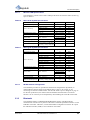
Implementing Magnetics
Refer to Table 14 for transformer requirements. Transformers meeting these requirements
are available from a variety of magnetic manufacturers. Designers should test and qualify
all magnetics before using them in an application. The transformers listed in Table 14 are
electrical equivalents, but may be not pin-to-pin compatible.
Table 14
Recommended Magnetic Modules
Manufacturer
Pulse Engineering
Delta
YCL
MAGCOM
Halo
Nano Pulse Inc.
Fil-Mag
Bel Fuse
Valor
Macronics
Bothhand
Part Number
PE-68515, H1078, H1012, H1102
LF8200, LF8221x
20PMT04, 20PMT05, PH163112 , YCL 0303, PH163539 *(Auto MDIX)
HS9001 , HS9016
TG22-3506ND, TD22-3506G1, TG22-S010ND, TG22-S012ND, TG110-S050N2
NPI 6181-37, NPI 6120-30, NPI 6120-37, NPI 6170-30
PT41715
S558-5999-01, S558-5999-W2
ST6114, ST6118
HS2123, HS2213
TS6121C,16ST8515,16ST1086
Figure 4 below shows an implementation example for use of a magnetic embedded in the
RJ-45 socket with integrated LEDs. Both center taps of the magnetic should be connected
to a 2.5V DC supply. Small LDO may be used for this purpose. Refer to Figure 5 for a
voltage source implementation example. Decouple 2.5V voltage with at least one large and
one small capacitors (10uF and 0.1uF respectively).
30-Dec-2010
CM-X300 Reference Guide Rev 1.31
23
CM-X300 CoM
Figure 4
Magnetic Interconnect Schematic
Figure 5
DC Source for Magnetic Center Taps
3.3.5
Serial Ports
CM-X300 incorporates 3 UARTs: one full function UART, one RX-TX only (console)
UART and one partial-function UART. All three UARTs share the same feature list, baud
rates and use the same programming model.
The UARTs share the following features:
24
Functionally compatible with 16550A and 16750
Ability to add or delete standard asynchronous communications bits (start, stop, and
parity) in the serial data
Independently controlled transmit, receive, line status, and data-set interrupts
Modem control functions (nCTS and nRTS on two of the three UARTs. The fullfunction UART additionally has nDSR, nDTR, nRI, and nDCD signals)
Auto-flow capability controls data I/O without generating interrupts:
nRTS (output) controlled by UART Receive FIFO
nCTS (input) from modem controls UART transmitter
Programmable serial interface:
CM-X300 Reference Guide Rev 1.31
30-Dec-2010
Functional Description
3.3.5.1
7- or 8-bit characters
Even, odd, or no parity detection
1 stop-bit generation
Baud-rate generation of 9.6K to 3.6M bps for all UARTs
False start-bit detection
64-byte Transmit FIFO
64-byte Receive FIFO
Complete status-reporting capability
Ability to generate and detect line breaks
Internal diagnostic capabilities that include:
Loopback controls for communications link fault isolation
Break, parity, and framing-error simulation
Fully prioritized interrupt system controls
Separate DMA requests for transmit and receive data services
Serial infrared asynchronous interface that conforms to the Infrared Data
Association (IrDA) specification
Full-Function UART
This is the CPU‘s UART1. The interface is routed to the CAMI COM-C serial port and
uses TTL-levels signaling. The port‘s pin descriptions are listed in Table 15.
Note: In module configuration C624M (PXA310 processor) these pins are re-defined for
use with the USB interface and not available on CAMI.
Table 15
3.3.5.2
Full-Function UART Signals
CM-X300 Signal
Name
Type
COM-C-RX
I
COM-C-TX
O
COM-C-CTS#
I
COM-C-RTS#
O
COM-C-DSR#
I
COM-C-DTR#
O
COM-C-DCD#
I
COM-C-RIN#
I
Description
Serial Data In: receives the serial data from the external serial device or
DCE into the internal serial port controller.
Serial Data Out: transmits the serial data from the internal serial port
controller to the external serial device or DCE.
Clear To Send: is sent back to the serial port to indicate that the external
data carrier equipment (DCE) is ready to accept data.
Request To Send: indicates to the external DCE that the internal serial port
controller is ready to send data.
Data Set Ready: indicates that the external DCE is ready to establish a
communication link with the serial port controller.
Data Terminal Ready: indicates to the external DCE that the serial port
controller is ready to communicate.
Data Carrier Detect: is sent back to the serial port from data carrier
equipment when it detects a carrier signal from a communications target.
Ring Indicate: is used by an external modem to inform the serial port that a
ring signal has been detected. A change in state on this signal by the
external modem can be configured to cause a modem status interrupt.
Console UART
This is the CPU‘s UART3. The interface is routed to the CAMI COM-A serial port and
uses RS-232-levels signaling. The port‘s pin descriptions are listed in Table 16.
Table 16
30-Dec-2010
Console UART Signals
CM-X300 Signal
Name
Type
COM-A-RX#
I
Description
Serial Data In: receives the serial data from the external serial device or
DCE into the internal serial port controller.
CM-X300 Reference Guide Rev 1.31
25
CM-X300 CoM
COM-A-TX#
3.3.5.3
O
Serial Data Out: transmits the serial data from the internal serial port
controller to the external serial device or DCE.
Partial-Function UART
This is the CPU‘s UART2. The interface is routed to the CAMI COM-D serial port and
uses TTL-levels signaling. The port‘s pin descriptions are listed in Table 17.
Table 17
3.3.6
Partial-Function UART Signals
CM-X300 Signal
Name
Type
COM-D-RX
I
COM-D-TX
O
COM-D-CTS#
I
COM-D-RTS#
O
Description
Serial Data In: receives the serial data from the external serial device or
DCE into the internal serial port controller.
Serial Data Out: transmits the serial data from the internal serial port
controller to the external serial device or DCE.
Clear To Send: is sent back to the serial port to indicate that the external
data carrier equipment (DCE) is ready to accept data.
Request To Send: indicates to the external DCE that the internal serial port
controller is ready to send data.
Local Bus
The CM-X300‘s local bus is the unbuffered CPU‘s Data Flash Interface (DFI). The DFI is
shared between the NAND Flash Controller (NFC) and Static Memory Controller (SMC).
The NAND Flash Controller (NFC) supports large- and small-block, 8-bit and 16-bit
NAND flash devices.
The Static Memory Controller (SMC) maintains multiple static-memory types, such as
synchronous and asynchronous flash devices, SRAM and SRAM-like variable-latency IO
devices (VLIO).
3.3.6.1
Local Bus Signal Description
The Static Memory Controller (SMC) signals are listed in Table 18. The NAND Flash
Controller (NFC) signals are listed in Table 19.
Note that some signals are shared between the two controllers.
Table 18
Local Bus Signals (SMC)
CM-X300 Signal
Name
26
Type
Description
DF-IO[15:0]
DF_CLE_nOE
DF_ALE_nWE
I/O
O
O
LB-CS[3:0]#
nXCVREN
O
LB-LUA#
O
LB-LLA#
O
DF-A[3:0]
O
Bidirectional data/address bus
Output enable
Write enable
Chip selects.
LB-CS3 may be configured as nXCVREN (External transceiver enable)
signal. It is asserted along with the Output Enable (DF_CLE_nOE) during
read accesses and one DF_SLCK cycle before the Write Enable
(DF_ALE_nWE) during write accesses.
0 = Enable transceiver
1 = Disable transceiver
Latch upper address. Used to latch the high-order address bits during the
upper address cycle.
Latch lower address. Used to latch the low-order address bits during the
lower address cycle.
Low-order address bits. Used as the lowest four address bits during an
asynchronous burst transfer of the values in the lower address cycle on the
DF-IO[15:0]
CM-X300 Reference Guide Rev 1.31
30-Dec-2010
Functional Description
Table 19
LB-BE[1:0]#
O
LB-RDY
I
Local Bus Signals (NFC)
CM-X300 Signal
Name
DF-IO[15:0]
DF-CS[1:0]#
DF_CLE_nOE
DF_ALE_nWE
DF-RE#
DF-WE#
DF-RB#
3.3.6.2
Data byte enable.
nBE0 corresponds to DF-IO[7:0]
nBE1 corresponds to DF-IO[15:8]
0 = Do not mask out corresponding byte
1 = Mask out corresponding byte
Variable-Latency I/O Ready signal for inserting wait states.
0 = Wait
1 = VLIO is ready
Type
I/O
O
O
O
O
O
I
Description
Bidirectional data/address bus
Chip selects
Command latch enable
Address latch enable
Read enable
Write enable
Ready/Busy_n (Low when Busy)
Static Memory Controller Address Map
The SMC has four separate partitions that are shown in Table 20.
Note: LB-CS0 is used internally as a chip select for the onboard Ethernet controller and
cannot be used externally on modules with ―E‖ option.
Table 20
SMC Address Map
Chip Select
LB-CS0
LB-CS1
LB-CS2
LB-CS3
3.3.6.3
Address Range
0x0000_0000–0x0FFF_FFFF (256 Mbyte)
0x3000_0000–0x3FFF_FFFF (256 Mbyte)
0x1000_0000–0x13FF_FFFF (64 Mbyte)
0x1400_0000–0x17FF_FFFF (64 Mbyte)
Local Bus Operation
For information about local bus AC characteristics refer to the Marvell PXA3xx (88AP3xx)
Processor Family EMPI document, section 7.2.
For information related to operation of the Data Flash Interface representing the local bus in
the CM-X300, refer to the Marvell® PXA3xx (88AP3xx) Processor Family Developers
Manual Vol. II: Memory Controller Configuration Developers Manual, sections 2 and 3.
3.3.7
Keypad
The CM-X300‘s keypad controller manages up to 8x6 matrix keys, up to eight direct keys,
and up to two rotary encoders, which can implement scroll keys, jog-dials, and
thumbwheels. The keypad controller provides an interface to two styles of keypads
simultaneously through the matrix and direct keypad interface. The controller manages both
manual and automatic scans.
Stable keypad activity that lasts longer than the debounce interval generates an interrupt. A
manual matrix scan can then be conducted to assert the scan lines sequentially. The row
readings for each column are read as they are scanned. If the ―ignore-multiple-keypress‖
policy is chosen, only one interrupt is generated for a debounced keypress. For example, if
three keys are pressed and held, only one interrupt is generated after the first key is pressed
and held. The column-scan signals are automatically asserted in sequence by the automatic
scan logic in the keypad controller, and the row readings are stored in the automatic scan
registers. Automatic scans can be initiated by either of the following methods:
30-Dec-2010
CM-X300 Reference Guide Rev 1.31
27
CM-X300 CoM
Table 21
If there is stable keypad activity for a period greater than the specified key
debounce interval while the automatic-scan-on-activity is enabled, completion of the
scan generates an interrupt.
If the automatic-scan is enabled, user software determines when to initiate an
automatic scan. This option does not generate an interrupt.
Keypad Signals
CM-X300 Signal
Name
Type
KP_MKOUT[5:0]
O
KP_MKIN[7:0]
I
KP_DKIN[3:0]
(shared with
GPIO88…85)
I
Description
Matrix Key Column-Scan Outputs
The keypad controller sends column-scan output signals to the columns of
the matrix keypad to detect any key(s) that are pressed. If an automatic
scan is occurring, these column-scan output signals are driven by the
automatic scan logic. At other times, they are driven by the settings of bits
MS5 through MS0 in the CPU‘s Keypad Interface Control (KPC) register.
Matrix Key Inputs (Returns)
The input signals from the matrix keypad (matrix-keypad row readings).
Direct Key Inputs
Signals from the direct keys and the rotary-encoder sensor.
KP_DKIN<1:0> are either input signals for direct keys 1 and 0 or input
sensor signals for rotary encoder A (if enabled).
KP_DKIN<3:2> are either input signals for direct keys 3 and 2 or inputsensor signals for rotary encoder B (if enabled).
Note: direct keys and rotary encoder inputs are shared with the Matrix Key Column-Scan
Outputs and other signals and may be made available through software.
3.3.8
LCD Interface
Features of the LCD controller are as follows:
Display modes
Single display modules
Passive panels: 24-bit-per-pixel color displays (no monochrome support)
Active panels: 8-, or 16 bit-per-pixel single-scan color displays without an
internal frame buffer
Smart panels: Up to 24-bit-per-pixel single-scan color displays with an internal
frame buffer
Display sizes (both portrait and landscape formats):
176 x 208
176 x 220
240 x 240
320 x 240 (QVGA)
320 x 320
640 x 480 (VGA)
800 x 480
28
The following display sizes are supported, but may have restrictions with
overlays enabled, BPP setting, and pixel clock frequency:
800 x 600
1024 x 768
1024 x 1024
64-entry (by 24 bits) output FIFO
Three 256-entry by 25-bit internal color-palette RAMs (one for each overlay and
base), programmable for automatic loading at the beginning of each frame
Command data RAM (16 x 9 bits) to hold command data
Pixel depths of 8, 16, 18 and 24 bpp RGB, and 19 and 25 bpp RGBT formats
CM-X300 Reference Guide Rev 1.31
30-Dec-2010
Functional Description
Table 22
LCD Signals
CM-X300 Signal
Name
3.3.8.1
Type
LCD-R[5:1]
O
LCD-G[5:0]
O
LCD-B[5:1]
O
LCD-LP
LCD-FRM
LCD-SCK
LCD-DE
O
O
O
O
Description
Red channel data for TFT panels. Bit 0 of the panel‘s red channel should
be connected to GND.
Green channel data for TFT panels.
Blue channel data for TFT panels. Bit 0 of the panel‘s blue channel should
be connected to GND.
HSYNC for TFT panels.
VSYNC for TFT panels.
Pixel clock.
Limitations of Display Controller Capabilities
The LCD controller provides a variety of programmable options including display type,
resolution, frame buffer, pixel depth, overlays, hardware cursor, and output data formatting.
Although all programmable combinations are possible, the available selection of displays
dictates which combinations of these programmable options are practical. The type of
external memory system used limits the bandwidth of the LCD DMA controller, which, in
turn, limits the resolution and type of screen that can be controlled. Use information below
to determine the maximum bandwidth of the internal bus that the LCD can use without
negatively affecting all other functions.
The equations in this section provide a way to estimate the LCD bandwidth needed to drive
an LCD panel with the PXA3xx processor. LCD bandwidth can affect overall system
performance by reducing the available system memory bus bandwidth. The CM-X300‘s
memory bus clock frequency is 130 MHz, data rate 260 MT/s. The LCD controller shares
the System Bus #1 with other devices (see Figure 6 below)
Figure 6
PXA300 Processor Block Diagram
The LCD controller can be programmed with timing values that control the refresh rate and
the needed LCD bandwidth for a specific LCD panel. The total needed memory bus
bandwidth can be defined as the LCD bandwidth plus the system memory bus bandwidth
used by any other running processes in the processor. When the total memory bus
30-Dec-2010
CM-X300 Reference Guide Rev 1.31
29
CM-X300 CoM
bandwidth needed exceeds the total available memory bus bandwidth, visible video
artifacts may be seen on the LCD panel.
Total Needed Memory Bus Bandwidth LCD Bandwidth System Memory Bus Bandwidth
The number of pixel clocks to send one line of pixels is calculated using the following
equation:
PixelClock s
(HSW 1) (BLW 1) (PPL 1) (ELW 1)
Line
Or:
PixelClock s
HSW BLW PPL ELW 4
Line
where:
HSW = Horizontal Sync Width
BLW = Beginning of Line Width
PPL = Pixels Per Line (Frame width -1)
ELW = End of Line width
The number of line clocks (HSYNC clocks) needed to send one frame is calculated using
the following equation:
LineClocks
(VSW 1) BFW (LPP 1) EFW
Frame
Or:
LineClocks
VSW BFW LPP EFW 2
Frame
where:
VSW = Vertical Sync Width
BFW = Beginning of Frame Width
LPP = Lines Per Page (Frame height – 1)
EFW = End of Frame Width
The number of pixel clocks to send one frame is calculated using the following equation:
PixelClock s LineClocks PixelClock s
Frame
Frame
Line
substituting:
PixelClock s
(VSW BFW LPP EFW 2) (HSW BLW ELW PPL 4)
Frame
Because LPP = Height – 1 and PPL = Width – 1, the following equation applies:
PixelClock s
(VSW BFW Height EFW 1) (HSW BLW ELW Width 3)
Frame
The refresh rate, which is the number of frames per second that the LCD controller is
fetching from memory and sending to the LCD panel, can be calculated using the following
equation:
Refresh Rate =
30
Pixel Clock Frequency
Pixel Clocks
Frame
CM-X300 Reference Guide Rev 1.31
30-Dec-2010
Functional Description
Pixel clock frequency is a parameter of the chosen resolution and frames per second, as
well as of the LCD-specific parameters, such as pixel clock wait states at the beginning and
end of each line, the number of line clocks inserted in the beginning and end of each frame.
Here's an example of some common video modes and their corresponding pixel clocks:
http://www.engr.udayton.edu/faculty/jloomis/altera/DE2/vga.html
The LCD data rate required for each plane to support the LCD panel selected for the system
is calculated using this formula:
Length Width Refresh Rate Bits per Pixel
Data Rate =
bps
8
The bits per pixel is the number of bits used in the memory to store each pixel. Memory
organization for pixel depth of 16bpp uses 2 bytes of data per pixel. With overlays enabled,
pixel depth is reduced to 15bpp still using 2 bytes.
The number of 4-beat burst operations (8 bytes/beat) that are generated by the LCD DMA
controller is as follows:
Data Rate
LCD DMA burst Count =
Burst/sec
32
The time consumed by the LCD refresh operation is then calculated by:
LCD refresh time (LCD DMA burst count Pdma) / second
The value of Pdma is the period in microseconds of LCD DMA four-beat burst, including
SDRAM precharge time. The time remaining within each second after deducting the LCD
refresh time is the time available for instruction and data fetches, hardware accesses, and
memory refresh operations. Use caution when setting system parameters, such as core
frequency, system frequency, memory frequency, and bus arbiter settings to ensure that
LCD FIFOs do not underrun due to bus latencies caused by other internal and external
peripherals. This caution applies especially for interrupt and polled modes that require a
longer time to service.
Benchmarking a real system remains the best way to estimate the LCD subsystem‘s
performance.
3.3.9
USB
3.3.9.1
USB Controllers
The CM-X300 features three USB controllers.
The USB device controller (UDC) is USB 1.1-compliant and supports all standard device
requests issued by any certified USB host controller. This is a full-speed compliant device
(does not support low-speed operation). This controller‘s interface is the CAMI USB2
Interface (only in C624 configurations).
The Universal Serial Bus 2.0 Device Controller (U2DC) supports both high-speed and fullspeed modes. The C624 configuration modules feature the industry standard Universal
Transceiver Macrocell Interface (UTMI), Version 1.05 transceiver for interfacing USB
devices. The transceiver‘s interface is routed to the CAMI USB3 Interface. In the C624M
modules a ULPI transceiver is used instead, connected to the CAMI USB2 Interface.
The Open Host Controller Interface (OHCI) Rev 1.0a-compatible USB host controller
supports both high-speed and full-speed modes. The available interfaces for the host
controller are the CAMI USB2 Interfacein C624 only non-W configuration modules and
the CAMI USB1 Interface in non-W configurations.
For a full description of the USB protocol and its operation, refer to the documents listed in
Table 2 and to Related Documents on page 9.
30-Dec-2010
CM-X300 Reference Guide Rev 1.31
31
CM-X300 CoM
3.3.9.2
USB Interfaces Routing
Table 23 below describes USB interfaces routing differences between C624 and C624M
module configurations.
Table 23
USB Interfaces
CAMI USB
Interface
USB1
USB2
USB3
3.3.9.3
CM-X300-C625
CM-X300-C625M
USB Host Controller
(differential port1 IF on PXA300)
USB Host Controller or
USB Device Controller
(OTG diff port 2 IF on PXA300)
USB 2.0 Device Controller (UTMI IF) on
PXA300
USB Host Controller
(single ended port 3 IF on PXA310)
USB2.0 Device Controller or
USB Host Controller
(ULPI IF on PXA310)
None
USB1 Interface
The USB1 CAMI interface is routed to the PXA300‘s differential USB port 1 or to the
PXA310‘s single ended USB port 3 (by means of the onboard transmitter). In both cases
this interface is controlled by the CPU‘s USB host controller. The module‘s integrated
Bluetooth uses this port; therefore it‘s not available with "W" option.
Table 24
3.3.9.4
USB1 CAMI Port Signals
CM-X300 Signal
Name
Type
{USBH-P, USBH-N}
I/O
Description
USB Full Speed Host Data
Differential pair that connects to the USB host controller.
USB2 Interface
This interface has different functionality in modules with PXA300 and PXA310 processor.
In the C624 modules (PXA300) this interface provides USB1.1 host/device and OTG
functionality and is routed to the PXA300‘s differential OTG USB port 2.
In the C624M modules (PXA310) this interface provides USB2.0 device or USB1.1 host
functionality and is routed to the PXA300‘s ULPI interface by means of an onboard ULPI
transmitter.
Table 25
USB2 CAMI Port Signals
CM-X300 Signal
Name
3.3.9.5
Type
{USB-OTG-P,
USB-OTG-N}
I/O
USB-OTG-ID
I
Description
USB Full Speed Host/Device/OTG and USB 2.0 Device Data
Differential pair that connects to either the USB host controller, the USB
device controller or USB 2.0 Device controller. On-The-Go functionality is
available on this port.
Provides the OTG ID configuration.
USB3 Interface
This interface is available only on the C624 (PXA300) modules. It provides USB 2.0 highspeed device functionality and is routed to the UTMI interface of PXA300 by means of an
onboard UTMI transmitter.
32
CM-X300 Reference Guide Rev 1.31
30-Dec-2010
Functional Description
Table 26
3.3.10
USB3 CAMI Port Signals
CM-X300 Signal
Name
Type
{USBD-P, USBD-N}
I/O
Description
USB 2.0 Device Data
Differential pair that connects to the USB 2.0 device controller.
MMC/SD/SDIO Controller
The Multimedia Card (MMC) and Secure Digital (SD/SDIO) controller (MMC/SD/SDIO
controller) provides a software-accessible hardware link between the processor and the
MMC stack (a set of memory cards). The MMC/SD/SDIO controller supports Multimedia
Card, Secure Digital, and Secure Digital I/O communication protocols.
The MMC module manages the MMC system, which is low-cost data storage and
communications system. The MMC module is based on the standards outlined in the
Multimedia Card System Specification Version 3.3.1. The SD module manages one
SD or SDIO card based on the standards outlined in the SD Memory Card
Specification Version 1.10 and SDIO Card Specification Version 1.0.
The MMC/SD/SDIO controller manages the translation protocol from a standard MMC bus
or from a serial peripheral interface (SPI) bus to the MMC stack. Software must select
either the MMC/SD/SDIO mode or SPI mode to establish the communication protocol for
the MMC/SD/SDIO controller.
3.3.10.1
MMC/SD/SDIO Controller Features
A response FIFO (MMC_RES)
Two transmit FIFOs (MMC_TXFIFO1 and MMC_TXFIFO2)
Two receive FIFOs (MMC_RXFIFO1 and MMC_RXFIFO2)
Two operating modes:
MMC/SD/SDIO mode for MMC, SD, and SDIO communication protocols.
SPI mode for the SPI communications protocol.
One-bit and 4-bit data transfers for MMC, SD, and SDIO communication protocols
Data transfer clock up to 26 MHz
Based on FIFO status, turn clock on and off to prevent overflows and under-runs
Support for all valid MMC and SD/SDIO protocol data-transfer modes
Interrupt-based application interface to control software interaction
Stream data transfers of 10 bytes or more
Multiple MMC cards for the MMC communications protocol
Only one SD or SDIO port can be used for SD or SDIO communications protocol
at one time.
Up to two MMC or SD/SDIO cards when the SPI communications protocol is used.
Mixed card types are supported only by the SPI communications protocol.
3.3.10.2
MMC/SD/SDIO Controller Interface Signals
Table 27
MMC and SD/SDIO Mode Signals
CM-X300 Signal
Name
MMC_CLK
MMC_CMD0
MMC_CMD1
MMC_DAT[3:0]
30-Dec-2010
Type
O
I/O
I/O
I/O
Description
Bus clock
Command and responses
Command and responses
Read and write data
CM-X300 Reference Guide Rev 1.31
33
CM-X300 CoM
Table 28
SPI Mode Signals
CM-X300 Signal
Name
Type
MMC_CLK
MMC_CMD0
MMC_CMD1
MMC_DAT0
MMC_DAT1
MMC_DAT2
MMC_DAT3
O
O
O
I
I
O
O
3.3.11
GPIO
3.3.11.1
I C Operated GPIOs
Description
SPI clock
Output for command and write data
Output for command and write data
Input for response token and read data
Signals an interrupt condition to the controller
CS0 chip select
CS1 chip select
2
The CM-X300 features 32 I2C-operated GPIO lines implemented using two I2C GPIO
extender IC‘s – Catalyst CAT9555 or compatible.
Table 29
GPIO Extenders
IC
A
B
Signals
Controlled
CAT9555
I2C Address
I2C_GPIO0_[7:0]
I2C_GPIO1_[7:0]
I2C_GPIO2_[7:0]
I2C_GPIO3_[7:0]
0b0100100x
0b0100101x
Note: ‗X‘ denotes R/W# bit.
Table 30
2
I C Operated GPIO Signals
CM-X300 Signal
Name
I2C_GPIO0_[7:0]
I2C_GPIO1_[7:0]
I2C_GPIO2_[7:0]
I2C_GPIO3_[7:0]
Table 31
I/O
Description
5V-tolerant GPIO
2
I C Operated GPIO DC Characteristics
Symbol
VIL
VIH
IOL
VOH
IIH
IIL
3.3.11.2
Type
Parameter
Low level input
voltage
High level input
voltage
Low level output
current
High level output
voltage
Input leakage
current
Input leakage
current
Condition
Min
Typ
Max
Unit
VCC typ = 3.2V
-0.5
–
0.3 x VCC
V
VCC typ = 3.2V
0.7 x VCC
–
5.5
V
VOL = 0.5V
VOL = 0.7V
8
10
8 to 20
10 to 24
–
mA
IOH = -10 mA
2.5
–
–
V
VI = VCC
–
–
1
uA
VI = VSS
–
–
-100
uA
CPU GPIO
The General-Purpose I/O (GPIO) provides 11 general-purpose input/output GPIO ports for
use in generating and capturing application-specific input and output. All ports are brought
out of the processor through alternate function multiplexing. More ports may be made
available when certain interfaces are not required by an application.
34
CM-X300 Reference Guide Rev 1.31
30-Dec-2010
Functional Description
When programmed as an input, a GPIO port can also serve as an interrupt source. At the
assertion of all resets, all ports are configured as inputs and remain inputs until they are
configured either by the boot process or by user software.
The direction of the GPIO ports is controlled by writing to the CPU‘s GPIO Pin Direction
register (GPDR2). When the GPIO pin is programmed as an output, the port is set by
writing to the GPIO Pin Output Set Register (GPSR2) and cleared by writing to the GPIO
Pin Output Clear Register (GPCR2). The Set and Clear registers can be written regardless
of whether the port is configured as an input or an output. The programmed output state
takes effect when the port is reconfigured as an output.
When the GPIO pin is programmed as an input, it can be configured to detect a rising edge,
falling edge, or both through the GPIO Rising-Edge Detect Enable Register (GRER2) and
the GPIO Falling-Edge Detect Enable Register (GFER2). The state of the edge-detect can
be read through the GPIO Edge Detect Status Register (GEDR2). These edge-detects can
be programmed to generate interrupts.
The value of each GPIO port is read through the GPIO Pin-Level Register (GPLR2). This
register can be read at any time and can confirm the port state for both input and output
configurations.
Note: GPIO18 is used internally by the u-boot when booting the module. It should not be
pulled-up or down by values lower than 100K on the baseboard.
Table 32
CPU GPIO Signals
CM-X300 Signal
Name
Type
GPIO[90:80]
I/O
GPIO[52:39]
I/O
GPIO[37:30]
I/O
GPIO[125:115]
GPIO[114:111]
GPIO[88:85]
I/O
I/O
I/O
Description
Dedicated GPIO (GPIO80..82 are available in C624 modules only. In the
C624M modules using these GPIO lines will interfere with USB host
function)
Camera interface GPIO (shared with CIF pins). These GPIO‘s are
available for GPIO use only in C624M modules. These signals are routed
to CAMI in C624 modules, too, but cannot be used as GPIO as they serve
as UTMI USB transmitter‘s interface onboard.
FFUART GPIO (shared with FFUART pins). Available only in C624
modules. These pins are used for ULPI transmitter interface in C624M
modules and are not available on CAMI.
Keypad GPIO (shared with keypad pins)
BTUART GPIO (shared with BTUART function pins)
SSP1 GPIO (shared with SSP1 pins)
Each of the 32-bit registers described maps its bits [31:0] to the GPIO pins [95:64].
Software should not modify any bits except [26:16] mapped accordingly to the CPU GPIO
signals [90:80] available on the CAMI.
Table 33
CPU GPIO Registers
Name
30-Dec-2010
Address
GPLR2
0x40E0_0008
GPDR2
2x40E0_0014
GPSR2
0x40E0_0020
Description
GPIO Pin-Level Register 2. Shows the current value of a particular port
(regardless of the programmed port direction):
0 = Port state is low
1 = Port state is high
GPIO Pin Direction Register 2. If a direction bit is set, the GPIO pin is an
output. If it is cleared, it is an input. A pair of set/clear registers (GSDR2
and GCDR2) is also provided to enable the setting and clearing of
individual bits of the GPDR2 register.
0 = Port configured as an input
1 = Port configured as an output
GPIO Pin Output Set Register 2. An output port is set by writing a 1 to its
corresponding bit in the GPSR2 (write-only register; reads return
unpredictable values).
0 = Port level unaffected.
1 = If the port is configured as an output, set the port level logic high
CM-X300 Reference Guide Rev 1.31
35
CM-X300 CoM
Name
36
Address
GPCR2
0x40E0_002C
GRER2
0x40E0_0038
GFER2
0x40E0_0044
GEDR2
0x40E0_0050
GSDR2
0x40E0_0408
GCDR2
0x40E0_0428
GSRER2
0x40E0_0448
GCRER2
0x40E0_0468
GSFER2
0x40E0_0488
GCFER2
0x40E0_04A8
Description
GPIO Pin Output Clear Register 2. An output port is cleared when a 1 is
written to the corresponding bit within the GPCR2 (write-only register;
reads return unpredictable values).
0 = Port level unaffected.
1 = If the port is configured as an output, clear the port level logic low.
GPIO Rising-Edge Detect-Enable Register 2. GRER2 bit is set to cause a
GEDR2 status bit to be set when the port transitions from Logic Level low
to Logic Level high.
0 = Disable rising-edge detect enable.
1 = Set the corresponding GEDR status bit when a rising edge is detected
on the GPIO port.
GPIO Falling-Edge Detect-Enable Register 2. GFER2 bit is set to cause a
GEDR2 status bit to be set when the port transitions from Logic Level high
to Logic Level low.
0 = No falling-edge detect enable.
1 = Set the corresponding GEDR status bit when a falling edge is detected
on the GPIO port.
GPIO Edge Detect Status Register 2 . When an edge-detect occurs on a
port that matches the type of edge programmed in the GRER2 and/or
GFER2 registers, the corresponding status bit is set in GEDR2. When a
GEDR2 bit is set, the CPU must clear it. GEDR2 status bits are cleared by
writing a 1 to them. Writing a 0 has no effect. Each edge-detect that sets
the corresponding GEDR2 status bit for GPIO pins can trigger an interrupt
request.
0 = No edge detect on the port as specified in GRER2 and/or GFER2.
1 = Edge detect on the port as specified in GRER2 and/or GFER2.
GPIO Pin Bit-Wise Set Direction Register 2 . If a direction bit is set, the
corresponding bit in GPDR2 is set and the GPIO function is configured as
an output. If it is cleared, no change in the GPIO functionality or the
GPDR2 register occurs.
0 = GPDR2 bit not affected.
1 = GPDR2 bit is set and GPIO function is set to OUTPUT.
GPIO Pin Bit-Wise Clear Direction Register 2 . If a direction bit is set, the
corresponding bit in GPDR2 is cleared and the GPIO function is
configured as an input. If it is cleared, no change in the GPIO functionality
or the GPDR2 register occurs.
0 = GPDR2 bit is not affected.
1 = GPDR2 bit is cleared and a GPIO function is set to INPUT.
GPIO Bit-Wise Set Rising-Edge Register 2. If a bit is set, the
corresponding bit in GRER2 is set and the GPIO function is configured to
cause a GEDR2 status bit to be set when the port transitions from Logic
Level zero (0) to Logic Level one (1). If the bit is cleared, no change in the
GPIO functionality or GRERx occurs
0 = GRER2 bit not affected.
1 = GRER2 bit is set.
GPIO Bit-wise Clear Rising-Edge Detect-Enable Register 2. If a bit is set,
the corresponding bit in GRER2 is cleared and the GPIO function is
configured to not cause a GEDR2 status bit to be set when the port
transitions from Logic Level zero (0) to Logic Level one (1). If the bit is
cleared, no change in the GPIO functionality or the GRER2 register occurs
0 = GRER2 bit not affected.
1 = GRER2 bit is cleared
GPIO Bit-Wise Set Falling-Edge Register 2. If a bit is set, the
corresponding bit in GFER2 is set and the GPIO function is configured to
cause a GEDR2 status bit to be set when the port transitions from logiclevel one (1) to logic-level zero (0). If the bit is cleared, no change in the
GPIO functionality or the GFER2 register occurs
0 = GFER2 bit not affected
1 = GFER2 bit is set
GPIO Bit-wise Clear Falling-Edge Detect-Enable Register 2. If a bit is set,
the corresponding bit in GFER2 is cleared and the GPIO function is
configured to not cause a GEDR2 status bit to be set when the port
transitions from logic-level one (1) to logic-level zero (0) If the bit is
cleared, no change occurs in the GPIO functionality or the GFER2 register.
0 = GFER2 bit not affected
1 = GFER2 bit is cleared
CM-X300 Reference Guide Rev 1.31
30-Dec-2010
Functional Description
Table 34
CPU GPIO DC Characteristics
Symbol
Parameter
Low level input
voltage
High level input
voltage
High level output
voltage
Low level output
voltage
VIL
VIH
VOH
VOL
RPULLUP,
RPULLDO
Condition
Min
Typ
Max
Unit
VCC typ = 3.2V
-0.3
–
0.2 x VCC
V
VCC typ = 3.2V
0.8 x VCC
–
VCC + 0.3
V
IOH = -1.5 to -18 mA
0.9 x VCC
–
VCC
V
IOH = -1.25 to -15 mA
VSS
–
0.1 x VCC
V
20
45
100
kOhm
Pull-up and pulldown resistance
WN
3.3.12
Camera Interface
The CM-X300 camera interface is represented by the CPU‘s Quick Capture Interface. It
connects the processor and a compatible external image-capture module, which consists of
a sensor providing RAW image data, a sensor with a minimal level of integrated processing
on RGB or YCbCr image data, or the combination of a sensor with more sophisticated
image-processing capability.
Note: The Camera Interface is available only in CM-X300 modules with PXA310
processor (C624M configuration).
The Quick Capture Interface operates in three modes:
Table 35
Preprocessed Still-Image/Video Capture mode. Supports image sensors and camera
modules that provide some level of preprocessing. The image data is in YCbCr 4:2:2
color space. The image data is captured through various interface options, optionally
scaled and/or bit sliced, and then formatted and packed before it is presented to
system memory resources.
RAW Still-Image Capture mode. Captures and formats image data to be processed
using algorithms targeting display or print quality. The image data is in the four
element Bayer pattern of RGGB color space. The data is captured through the
various interface options, optionally corrected for dead pixels, companded, blacklevel clamped, and then packed before it is presented to memory resources.
RAW Video-Image Capture mode. Offers the digital viewfinder function and the
video-clip capture function at a CIF, QCIF, SIF, or QSIF resolution. The sensor
provides image data in the RAW RGGB color. The integrated pixel processing chain
supports the conversion to RGB 8:8:8 and YCbCr 4:2:2 (and YCbCr 4:2:0 for
PXA31x processor) color space through several functional units, which include:
Spatial scaling unit (SSU)
Pixel substitution unit (PSU)
Companding/black-level clamp/gamma correction unit (CGU)
Color synthesis unit (CSU)
Color management unit (color space conversion and correction) (CMU)
Camera Interface Signals
CM-X300 Signal
Name
30-Dec-2010
Type
CIF_DD[9:0]
I
CIF_MCLK
O
CIF_PCLK
I
Description
Data lines to transmit 8 or 10 bits of data at a time. These pins may be
defined as GPIO[48..39] in a camera-less application.
Programmable clock output used by the image sensor.
This pin may be defined as GPIO49 in a camera-less application.
Pixel clock used by the Quick Capture Interface to clock the pixel data into
the input FIFO.
This pin may be defined as GPIO50 in a camera-less application.
CM-X300 Reference Guide Rev 1.31
37
CM-X300 CoM
CM-X300 Signal
Name
Type
CIF_FV
I/O
CIF_LV
I/O
3.3.13
Audio Subsystem
3.3.13.1
Audio I/O
Description
Frame start or alternate synchronization signal used by the sensor to signal
frame readout or as an external vertical sync. For CIF_PCLK speeds > 26
MHz, the sensor CIF_FSYNC signal must not be active until at least 2
pixel clocks after the last valid data of a frame.
This pin may be defined as GPIO52 in a camera-less application.
Line start or alternate synchronization signal used by the sensor to signal
line readout or as an external horizontal sync. For CIF_PCLK speeds > 26
MHz, the sensor CIF_HSYNC signal must not be active until at least 2
pixel clocks after the last valid data of a line.
This pin may be defined as GPIO51 in a camera-less application.
The CM-X300 audio subsystem uses the Wolfson WM9715L as an AC‘97 Rev 2.2
compatible stereo codec. Its analog audio interfaces include stereo line output which may
also drive a 400mW speaker or 45mW headphone, mono microphone input and stereo line
input.
Table 36
Audio I/O Signals
CM-X300 Signal
Name
AUD-SPDIF
AUD-INL-MIC
AUD-INR
AUD-OUTL
AUD-OUTR
3.3.13.2
Type
O
AI
AI
AO
AO
Description
SPDIF Digital Audio Output
Left Line Input and Microphone Input
Right Line Input
Left Output (Speaker, Line or Headphone)
Right Output (Speaker, Line or Headphone)
AC’97 Bus
The AC‘97 bus is available on the same CAMI connector pins as the audio I/O signals,
when the ―AT‖ option is not engaged.
Table 37
AC’97 Bus Signals
CM-X300 Signal
Name
AUD-SPDIF/
AC97_RST#
AUD-INR/
AC97_SDOUT
AUD-OUTL/
AC97_SDIN
AUD-INL-MIC/
AC97_BITCLK
AUD-OUTR/
AC97_SYNC
3.3.14
Type
Description
O
Asynchronous, active-low CODEC reset. The CODEC registers arereset
when AC97_RST is asserted
O
Serial audio output data to CODEC, for digital-to-analog conversion
I
Serial audio input data, from primary CODEC
I
12.288 MHz bit-rate clock
O
48-kHz frame indicator and synchronizer
Touch Panel Interface
The CM-X300 features a resistive touchpanel interface. It has a 12-bit resolution and
supports 4-wire panels only.
38
CM-X300 Reference Guide Rev 1.31
30-Dec-2010
Functional Description
Table 38
3.3.15
Touch Panel Interface Signals
CM-X300 Signal
Name
Type
TS-XP
TS-YP
TS-XM
TS-YM
AI
AI
AI
AI
Description
X+ (Right)
Y+ (Top)
X- (Left)
Y- (Bottom)
Power
The CM-X300 connects to power sources through the dedicated pins on the CAMI
connectors listed in the Table 39 below.
Table 39
Power Signals
CM-X300 Signal
Name
Type
GND
VBAT
VCHRG
VCC-RTC
P
P
P
P
Description
Ground (common wire)
Battery/DC supply voltage
Charger voltage
RTC backup supply voltage
The main supply voltage for CM-X300 should be connected to VBAT pins on the CAMI.
When an external regulator is used for VBAT (CM-X300 without the ―B‖ option) VCHRG
pins can be left unconnected.
If a battery is used for VBAT (CM-X300 with the ―B‖ option) VCHRG pins should be
connected to an external DC Charger. Battery charge current is drawn from the VCHRG
input.
The operating conditions for the charger and the battery are listed below.
Table 40
Battery and Charger Operating Conditions
Parameter
VBAT voltage
VCHRG voltage
Battery type
VCC-RTC voltage
3.3.16
Description
With “B” option: VBAT should be in 3.4V to 4.5V voltage range.
CM-X300 will not boot until VBAT is within this range.
If the battery is completely drained (below 3.2V), then pre-charge mode is started
when a charger has been detected. The current flow into the battery will be 40mA
nominal. If within 60 min. the VBAT reached 3.2V, CM-X300 will be powered on,
otherwise the pre-charge mode will be disabled.
If VBAT reaches 4.7V (for example, when battery suddenly disconnects while
charger is connected and powered), CM-X300 will be turned off immediately.
Without “B” option: VBAT should be 3.3V for normal operation.
When battery is not required by design, external regulator voltage should not fall
below 3.2V.
4.6 to 10.0 V
The internal battery charger supports the following battery chemistries:
Single-Cell Li-Ion at 4.1V
Single-Cell Li-Ion at 4.2V
Li-Polymer Pack
1.5 to 5.0 V
Typical supply current 390 nA @ 3.0 V
System Signals
The CM-X300‘s system signals are listed in Table 41.
30-Dec-2010
CM-X300 Reference Guide Rev 1.31
39
CM-X300 CoM
Table 41
System Signals
CM-X300 Signal
Name
Type
WP1#
I
RST-IN#
I/OD
EXTWAKE#
I
ONKEY#
I
IRQ
I
BOOTENA#
I
RST-OUT#
OD
SYS_EN
O
EXT_TBAT
I
3.3.17
I2C Bus
Table 42
I C Signals
3.3.18
Description
Hardware write protect for the the entire onboard Data Flash. Prevents all
program/erase operations.
Pulled up to 3.3V internally. Connect to GND to write-protect.
Reset input to CPU and power-on reset output. Pulled up to 3.3V
Processor‘s wakeup signal. Pulled down to GND. Pull to 3.3V to generate
wakeup event.
Connects to ON/OFF button. Pull to GND to switch the Power
Management IC ON or OFF. Tying this line to GND for 5 s or more
generates a hard reset.
Processor‘s interrupt request. Connects to the pin GPIO19.
May be used to disable internal Data Flash. Normally pulled to GND. Pull
to 3.3V to disable.
Active low output, indicated reset state of the CPU‘s Services Power
Management Unit
System Enable for System Peripheral Power Supply. This output, when
deactivated, signals that the system is entering S3/D4/C4 mode
Should be connected to the battery‘s internal NTC resistor to make its
temperature measurement by the charger function possible.
2
CM-X300 Signal
Name
Type
I2C-CLK
I2C-DATA
O
I/O
Description
I2C bus clock
I2C bus bidirectional data
Synchronous Serial Port (SSP)
The CM-X300 features two synchronous serial ports (SSP). These are the PXA3xx ports
SSP1 and SSP3. PXA3xx port SSP1 is available as an alternate function on pins
GPIO[85:88]. Port SSP3 is routed to CAMI connector B.
Table 43
Table 44
40
SSP1 Port Signals
CM-X300 Signal
Name
Type
SSPSCLK
I/O
SSPSFRM
I/O
SSPTXD
O
SSPRXD
I
Description
Synchronous Serial Protocol Serial Clock. Shared with pin GPIO85.
Controls the timing of a serial transfer. SSPSCLK can be generated
internally (master mode) or taken from an external source (slave mode)
Synchronous Serial Protocol Serial Frame Indicator. Shared with pin
GPIO86. Indicates the beginning and the end of a serialized data sample.
The SSPSFRM can be generated internally (master mode) or taken from an
external source (slave mode).
Synchronous Serial Protocol Transmit Data. Shared with pin GPIO87.
Serial data out.
Synchronous Serial Protocol Receive Data. Shared with pin GPIO88.
Serial data in.
SSP3 Port Signals
CM-X300 Signal
Name
Type
SSPSCLK3
I/O
SSPSFRM3
I/O
Description
Synchronous Serial Protocol Serial Clock. Controls the timing of a serial
transfer. SSPSCLK can be generated internally (master mode) or taken
from an external source (slave mode)
Synchronous Serial Protocol Serial Frame Indicator. Indicates the
beginning and the end of a serialized data sample. The SSPSFRM can be
generated internally (master mode) or taken from an external source (slave
mode).
CM-X300 Reference Guide Rev 1.31
30-Dec-2010
Functional Description
3.3.18.1
CM-X300 Signal
Name
Type
SSPTXD3
SSPRXD3
O
I
Description
Synchronous Serial Protocol Transmit Data. Serial data out.
Synchronous Serial Protocol Receive Data.Serial data in.
SSP Features
The SSP port features are:
3.3.18.2
Directly supports Texas Instruments* Synchronous Serial (SSP) and Motorola*
Serial Peripheral Interface (SPI).
The Inter-IC Sound (I2S) protocol is supported by programming the Programmable
Serial Protocol (PSP). PSP format is only supported for emulation of the I 2S
protocol.
Data sample sizes can be set to 8, 16, 18 or 32 bits
One FIFO for transmit data (TXFIFO) and a 2nd, independent, FIFO for receive
data (RXFIFO). For non-packed data mode, the two FIFOs are each 16 rows deep x
32 bits wide for a total of 16 samples.
FIFO packed mode allows double depth FIFOs if the samples are 8 bits or 16 bits
wide. For packed data mode, both FIFOs are 32 locations deep x 16 bits wide for a
total of 32 samples.
Master mode and slave mode operation supported
A maximum serial bit-rate supported of 13 Mbps.
Receive-without-transmit operation
Network mode with up to eight time slots for PSP formats, and independent
transmit/receive in any/all/none of the time slots.
Turning the SSP Port On
In order to enable SSP function on pins GPIO[85:88], their alternate functions should be
modified in the corresponding configuration registers. A binary value ‗001‘ must be written
into the bits [2:0] of the multi-function pin registers (MFPR) at addresses 0x40E104E8,
0x40E104EC, 0x40E104F0, 0x40E104F4 using a read-modify write access.
3.3.19
PWM Controller
The PWM function enables the control of leading- and falling-edge timing of two output
channels. The edge timing can be set up to run indefinitely or adjusted on the fly to adapt to
variable requirements. Power-saving modes include the ability to stop the internal clock
source (PSCLK_PWM) used to source the PWM and drive the PWM_OUT signals to a
steady high or low state.
The frequency range supporting a 50% duty cycle varies from 198.4 Hz to 6.5 MHz. Other
duty-cycle options depend on the choice of preferred frequency.
Table 45
30-Dec-2010
PWM Signals
CM-X300 Signal
Name
Type
PWM1-OUT
I/O
PWM2-OUT
I/O
Description
Pulse-width modulated signal, output of the CPU‘s PWM1 controller. This
pin is used internally by the u-boot when booting the module. It should not
be pulled-up or down by values lower than 100K on the baseboard.
Pulse-width modulated signal, output of the CPU‘s PWM2 controller
CM-X300 Reference Guide Rev 1.31
41
CM-X300 CoM
3.3.19.1
PWM Features
3.3.19.2
Four pulse-width modulated signal channels
Enhanced period controlled through 6-bit clock divider and 10-bit period counter
10-bit pulse control
PWM Operation
Figure 7 shows the block diagram for the PWM control logic.
Figure 7
PWM Block Diagram
To program the PWM controller, determine the period and pulse-width values. The period
value is based on two registers, PWMPCR2 and PWMCR2.
Figure 8
Basic PWM Waveform
The output waveform in Figure 8 is derived by writing the PWMPCRx register with a value
of 10(0x00A) and writing the PWMDCRx register with 0x06.
Pulse-width modulated signals, once programmed, output a specified waveform until the
value in any associated register is altered. The time from the register change until the
associated signal change depends on PWMPCRx[PV]:
42
CM-X300 Reference Guide Rev 1.31
30-Dec-2010
Functional Description
Figure 9
For PWMPCRx[PV] values 0x005 and larger—After a register value is altered, the
PWM_OUTx signal changes when the previously programmed waveform cycle is
complete.
For PWMPCRx[PV] values less than 0x005—After a register value is altered, the
PWM_OUTx signal changes after two waveform cycles
Effect of PWMCR2 Settings
Programming PWMCRx[PRESCALE] configures the prescaled counter clock. Two timing
examples are provided in Figure 9. Both examples have the PWMDCRx and PWMPCRx
registers set with the same 50% duty cycle setting. The first example shows the effect on
the scaled counter clock effectively being divided by two with a setting of 0x01, while the
second example shows the scaled counter clock being divided by four with a setting of
0x03. See Section 3.3.19.4 for more information regarding the calculation of waveform
values.
3.3.19.3
PWM Reset Sequence
During system reset, the PWMCRx and PWMDCRx registers are reset to 0x0 and the
PWMPCRx register is set to 0x004. Reset places the PWMx_OUT channel in a steady low
state. The PWMx_OUT channel remains reset to 0x0 until the PWMDCRx register is
programed with a non-zero value. Therefore,system reset results in no pulse-width
modulated signal.
3.3.19.4
Programming Considerations
The PWM uses three registers to configure the output of the PWMx signal: PWMCRx,
PWMDCRx, and PWMPCRx.
PWM timing is based on the input clock to the PWMx controller, PSCLK_PWMx, which is
fixed at 13 MHz. This signal is divided by (PWMCRx[PRESCALE] + 1) to generate the
scaled counter clock. The 6-bit PRESCALE field allows the input clock to be divided by
values between 1 (PRESCALE = 0) and 64 (PRESCALE = 63). The scaled counter clock is
further divided by contents of the PWMDCRx and PWMPCRx registers to generate the
duty cycle and period of the PWMx signal.
30-Dec-2010
Use the following equation to calculate the frequency of the scaled counter clock:
Scaled counter clock frequency = 13 MHz / (PWMCRx[PRESCALE] + 1)
CM-X300 Reference Guide Rev 1.31
43
CM-X300 CoM
Use the following equation to calculate the cycle time of the scaled counter clock:
Scaled counter clock cycle time = 76.9 ns x (PWMCRx[PRESCALE] + 1)
Both the period and the duty cycle of the PWM are based on the scaled counter clock cycle
time. The PWMx_OUT signal is asserted for the number of scaled counter clock cycles
equal to PWMDCRx[DCYCLE].
To calculate the duty cycle time of the PWM,use the following equation:
Duty cycle time = Scaled counter clock cycle time x PWMDCRx[DCYCLE]
which also equals:
Duty cycle time = 76.9nS x (PWMCRx[PRESCALE] + 1) x PWMDCRx[DCYCLE]
The PWM Period Control register (PWMPCRx) determines the number of scaled counter
clock cycles each PWM period contains. The actual number of clocks is the value of
PWMPCRx[PV] plus one. When the RST comparator equals (PWMPCRx[PV]+1), the
comparators and the flip-flop are reset, and the values of the PWMDCR_HOLDx,
PWMCR_HOLDx, and PWMPCR_HOLDx registers are loaded from the control block.
Use the following equation to calculate the period of the PWM:
PWM period = Scaled Counter Clock period x (PWMPCRx[PV] + 1)
which also equals:
PWM cycle time = 76.9nS x (PWMCRx[PRESCALE]+1) x (PWMPCRx[PV] + 1)
Calculate values based on the necessary PWM cycle time and duty cycle with the
following equations:
Choose a PWMCRx[PRESCALE] value that is appropriate for all your PWM
outputs.
PWMPCRx[PV] = PWM cycle time / (76.0nS X (PWMCRx[PRESCALE] + 1)) – 1
Duty cycle time = PWM cycle time * Duty Cycle%
PWMDCRx[DCYCLE] = Duty cycle time / (76.0nS X (PWMCRx[PRESCALE] + 1
))
For example, to create a 60% duty cycle 500 kHz signal, set PWMCRx[PRESCALE] to 0,
PWMPCRx[PV] to 26 (0x1A), and PWMDCRx[DCYCLE] to 16 (0x10).
Note: To produce a toggle of the signal, the value of the PWMPCRx[PV]must be equal to
or greater than PWMDCRx[DCYCLE]. If PWMPCRx[PV] is less than
PWMDCRx[DCYCLE], the PWMx_OUT signal remains high. If PWMDCRx[DCYCLE]
equals zero, the signal remains low.
The PWMDCRx[FD] bit determines if PWMx_OUT is always asserted. When this bit is
set, PWMx_OUT remains high until PWMDCRx[FD] is cleared.
3.3.19.5
PWM Register Summary
The PWM contains three registers that control the clock, the period, and the duty cycle
timing of the PWMx_OUT.
Table 46
PWM Registers
Address
0x40C0_0000
0x40C0_0004
0x40C0_0008
0x40B0_0010
0x40B0_0014
0x40B0_0018
44
Description
PWM 1 Control Register (PWMCR1)
PWM 1 Duty Cycle Register (PWMDCR1)
PWM 1 Period Control Register (PWMPCR1)
PWM 2 Control Register (PWMCR2)
PWM 2 Duty Cycle Register (PWMDCR2)
PWM 2 Period Control Register (PWMPCR2)
CM-X300 Reference Guide Rev 1.31
30-Dec-2010
Functional Description
3.3.19.6
PWM Control Register (PWMCRx)
The PWM Control register (PWMCRx), defined in Table 47, configures the behavioral
characteristics of the PWM shutdown response and the divisor for the input clocks to the
PWM control unit that configures the frequency of the scaled counter clock.
This is a read/write register. Ignore reads from reserved bits. Write 0b0 to reserved bits.
Table 47
3.3.19.7
PWM Control Register
Bits
Access
Name
31:7
–
–
6
R/W
SD
5:0
R/W
PRESCALE
Description
Reserved
Pulse Width Modulator Shutdown Mode:
0 = Graceful shutdown of PWMx when the PXA3xx
processor family stops the clocks to the PWM.
1 = Abrupt shutdown of PWMx when the PXA3xx
processor family stops the clocks to the PWM.
The scaled counter clock frequency is:
PSCLK_PWMx / (PRESCALEx + 1)
PWM Duty Cycle Register (PWMDCRx)
The PWMx Duty Cycle register (PWMDCRx), defined in Table 48, configures the duty
cycle of the PWMx_OUT signal.
PWMDCRx[DCYCLE] specifies the number of scaled counter clocks that PWMx_OUT is
asserted during each cycle of the PWMx_OUT. Refer to Section 3.3.19.4 for details on
calculating the value of PWMDCRx[DCYCLE].
If PWMDCRx[FD] is set, PWMx_OUT remains high until PWMDCRx[FD] is cleared.
This results in a duty cycle of 100%. Typically, PWMDCRx[FD] is cleared and the duty
cycle of PWMx_OUT is a function of PWMDCRx[DCYCLE].
This is a read/write register. Ignore reads from reserved bits. Write 0b0 to reserved bits.
Table 48
PWM Duty Cycle Register
Bits
Access
Name
31:11
–
–
10
R/W
FD
9:0
3.3.19.8
R/W
DCYCLE
Description
Reserved
Full Duty Cycle:
0 = PWMx_OUT is determined by DCYCLE value.
1 = PWMx_OUT is continuously asserted.
Duty Cycle of PWMx_OUT:
0 = PWMx_OUT is continuously de-asserted.
1 = PWMx_OUT is high for the number of 13-MHz
clock periods equal to
PWMDCRx[DCYCLE] x (PWMCRx[PRESCALE]+1),
If FD is set, DCYCLE has no effect on the output of
PWM
PWM Period Control Register (PWMPCRx)
The Period Control registers (PWMPCRx), defined in This is a read/write register. Ignore
reads from reserved bits. Write 0b0 to reserved bits.
Table 49, configures the cycle time of the PWMx_OUT signal.
PWMPCRx[PV] specifies the number of scaled counter clocks (plus one) in each cycle of
the PWMx_OUT. Refer to Section 3.3.19.4 for details on calculating the value of
PWMPCRx[PV].
If this register is cleared the PWMx_OUT signal maintains in a high state.
This is a read/write register. Ignore reads from reserved bits. Write 0b0 to reserved bits.
30-Dec-2010
CM-X300 Reference Guide Rev 1.31
45
CM-X300 CoM
Table 49
46
PWM Period Control Register
Bits
Access
Name
31:10
–
–
9:0
R/W
PV
Description
Reserved
Period Value:
The value of scaled clock cycles per cycle of PWMx_OUT
plus one.
If all zeros are written to this register the signal remains
high.
CM-X300 Reference Guide Rev 1.31
30-Dec-2010
Baseboard Interface
4 BASEBOARD INTERFACE
4.1 CAMI Connectors
The CM-X300 connects to the external world through P1, P2 – 0.6 mm pitch 140-pin
connectors.
4.1.1
Connectors Type and Layout
Table 50
CAMI Connectors
Reference
Mfg.
CM-X300 connector P/N
Baseboard (mating) connector P/N
P1, P2
AMP
1-5353183-0
1-5353190-0 or CON140
Mating connectors and standoffs are available from CompuLab, see [prices] >>
[accessories] links in the CompuLab's website. CompuLab's p/n name for AMP/Tyco 15353190-0 connector is "CON140".
4.1.2
Standoffs
CM-X300 has four mounting holes for standoffs. Standoff is implemented by two parts:
screw and spacer.
Table 51
Standoff Part List
Part
Screw
Spacer
30-Dec-2010
Description
M2, Pan head, Philips, 3.5mm +0.1mm Length, stainless Steel,
Nickel or Zinc plating
Spacer, M2, L = 4.14mm, Brass, Tin
coating
Manufacturer and P/N
Acton InoxPro BF22102003
Federal Screw Works DF1402003
WORLD BRIDGE MACHINARY 380J52020
World Bridge Machinery M2, L = 4.14mm
CM-X300 Reference Guide Rev 1.31
47
CM-X300 CoM
4.2 Mechanical drawings
CM-X300 Top View
Q2
R3 4
Q1
Figure 10
U1 9
X5
U1 3
U1
U2
ANT2
X4
J3
L6
U3
L7
J1
U2 3
ANT1
Figure 11
CM-X300 Bottom (X-Ray view – as aeen from the top side)
140
2
X1
P1
1
139
140
2
P2
1
U20
U21
139
U4
U15
X6
U16
C1
U14
U5
1. All dimensions are in millimeters
2. Height of all components except X5 and C1 is <2mm
3. The height of X5 is 2.5mm typ., of C1 is 2.0mm typ.
4. C1 is non-isolated, do not place components under C1 on the carrier board
5. CAMI connectors provide 4mm board-to-board clearance
6. Board thickness is 1.2mm
Mechanical drawings are available in DXF format from the CompuLab's website, following
[Developer] >> [CM-X300] >> [CM-X300 - Dimensions and Connectors Location] links.
48
CM-X300 Reference Guide Rev 1.31
30-Dec-2010
Baseboard Interface
4.3
Baseboard Design Guidelines
Assure that all power pins are connected as specified in ―Power‖ section of this manual.
GND must be implemented by plane, rather than traces.
It is recommended to put several 100 nF and 10/100 uF capacitors between VBAT/VCHRG
and GND near the mating connectors.
It is recommended to connect 3 out of the 4 standoff holes of the baseboard to GND, in
order to improve EMC. The top right hole of the baseboard should be isolated, for
compatibility with future CAMI modules (referring to module's orientation drawings).
Except of power connection, no other connection is mandatory for CM-X300 operation. All
powerup electronics and all required pullups/pulldowns are found on the module.
If for some reason you decide to place external pullup or pulldown resistor on certain signal
(for example - on GPIO's), check the documentation of that signal as provided in this
manual. Certain signals have on-board pullup/pulldown resistors required for proper
initialization. Overriding their values by external components will disable board operation.
You must be familiar with signal interconnection design rules. There are many sensitive
groups of signals. For example:
Ethernet and USB signals must be routed in differential pairs and by controlled
impedance trace.
Audio input must be decoupled from possible sources of baseboard noise.
Local bus signals must be buffered in most cases.
Be careful when placing component under the CM-X300 module. CAMI connector
provides 4mm mating height. Bear in mind that there are components on the underside of
the CM-X300. In general, maximum allowable height for components placed under the
CM-X300 is 2mm.
See the SB-X300 baseboard reference design schematics.
4.4 Baseboard Troubleshooting
Using grease solvent and soft brush, clean contacts of mating connectors of both module
and baseboard. Remainders of soldering paste can prevent proper contact. Take care to let
the connectors and the module dry entirely before re-applying power – otherwise corrosion
may occur.
Using oscilloscope, check voltage levels and quality of VBAT and VCHRG power
supplies. It should be as specified in ―power‖ section. Check that there is no excessive
ripple or glitches. First perform the measurements without plugging in the module. Then
plug in the module and measure again. Measurement should be performed on the pins of
mating connector.
Using oscilloscope verify that GND pins of mating connector are indeed at zero voltage
level, and there is no ground bouncing. Module must be plugged in during the test.
Create "minimum system" - only power, mating connectors, the module, and serial
interface.
Check if the system starts properly. In system larger than minimum, the possible sources of
disturbance could be:
30-Dec-2010
Devices improperly driving local bus
External pullup/pulldown resistors overriding module‘s on-board values, or any
other components creating the same "overriding" effect.
Bad power supply.
CM-X300 Reference Guide Rev 1.31
49
CM-X300 CoM
In order to avoid possible sources of disturbance, it is strongly recommended to start with
minimal system and then add/activate off-board devices one by one.
Check for existence of soldering shorts between pins of mating connectors. Even if signals
are not used on the baseboard, shorting them on the connectors can disable module's
operation. Initial check can be performed using microscope. However, if microscope
inspection finds nothing, it is advised to check using X-ray, because often solder bridges
are deeply beneath the connector's body. Note that solder shorts are the most frequent factor
disabling module's start.
Check possible signals shorting due to errors of baseboard PCB design or assembling.
Improper function of customer baseboard can accidentally delete bootup code from CMX300, or even damage module's hardware permanently. Before every new attempt of
activation, check that your module is still functional with CompuLab's SB-X300 baseboard.
It is recommended to assemble more that one baseboard for prototyping, in order to allow
quick sorting out of problems related to specific board assembly.
50
CM-X300 Reference Guide Rev 1.31
30-Dec-2010
Operating Temperature Ranges
5 OPERATING TEMPERATURE RANGES
The CM-X300 is available with three options of operating temperature range.
Table 52
30-Dec-2010
CM-X300 Temperature Range Options
Range
Temp.
Commercial
0o to 70o C
Extended
-20o to 70o C
Industrial
-40o to 85o C
Description
Sample cards from each batch are tested for the lower and upper
temperature limits. Individual cards are not tested.
Every card undergoes short test for the lower limit (-20o C)
qualification.
Every card is extensively tested for both lower and upper limits and
at several midpoints.
CM-X300 Reference Guide Rev 1.31
51
CM-X300 CoM
6
POWER CONSUMPTION
Typical power consumption has been measured on module inserted into SB-X300 carrier
board with no peripherials connected and 3.05V power source connected to the VBAT rail.
Measurements do not include power drawn by the SB-X300 base board.
Table 53
CM-X300 Power Consumption (BT and Wi-Fi enabled)
Parameter
Value, mA
Imax
Iidle
Isusp
470
350
16.5
Note
Absolute maximum on CPU 100% load
OS idle state average value
Suspend mode typical value
In the following table the values are for the SW package which does not enable Bluetooth
and Wireless Ethernet power supply.
Table 54
52
CM-X300 Power Consumption (BT and Wi-Fi disabled)
Parameter
Value, mA
Imax
Iidle
Isusp
345
185
16.5
Note
Absolute maximum on CPU 100% load
OS idle state average value
Suspend mode typical value
CM-X300 Reference Guide Rev 1.31
30-Dec-2010