1
SGI™ 1400 Server Family
Maintenance and Upgrades Guide
Document Number 007-3948-001
CONTRIBUTORS
Writing contributions by Mark Schwenden
Illustrated by Cheri Brown
Production by Heather Hermstad and David Clarke
Engineering contributions by Jim Oliver, Courtney Carr, Joan Eslinger, and Chander
Kant
St. Peter’s Basilica image courtesy of ENEL SpA and InfoByte SpA. Disk Thrower
image courtesy of Xavier Berenguer, Animatica.
© 1999, Silicon Graphics, Inc.— All Rights Reserved
The contents of this document may not be copied or duplicated in any form, in whole
or in part, without the prior written permission of Silicon Graphics, Inc.
LIMITED AND RESTRICTED RIGHTS LEGEND
Use, duplication, or disclosure by the Government is subject to restrictions as set
forth in the Rights in Data clause at FAR 52.227-14 and/or in similar or successor
clauses in the FAR, or in the DOD, DOE, or NASA FAR Supplements. Unpublished
rights reserved under the Copyright Laws of the United States.
Contractor/manufacturer is Silicon Graphics, Inc., 1600 Amphitheatre Pkwy.,
Mountain View, CA 94043-1351.
Silicon Graphics is a registered trademark and SGI and the Silicon Graphics logo are
trademarks of Silicon Graphics, Inc. Pentium is a registered trademark and Xeon is a
trademark of the Intel Corporation. All other third party brands and names
mentioned in this document are the property of their respective owners.
SGI™ 1400 Server Family Maintenance and Upgrades Guide
Document Number 007-3948-001
Contents
List of Figures
vii
List of Tables ix
About This Guide xiii
1.
Working Inside the System 1
Tools and Supplies Needed 1
Safety: Before You Remove the Access Cover 1
Warnings and Cautions 2
Removing the System Access Cover 3
Installing the Access Cover 3
Working in the Subchassis and Electronics Bay 5
Installing PCI Boards 7
Removing a PCI option Board 9
Removing the Front Panel Board 9
Installing the Front Panel Board 10
Removing the Diskette Drive 11
Installing the Diskette Drive 12
Peripheral Drives 13
Drive Cabling Considerations 13
IDE Requirements 13
SCSI Requirements 14
Installing 5.25-inch Peripherals in the Front Bays 14
Removing a 5.25-inch Peripheral from the Front Bay 18
Installing or Replacing the SCSI-B Cable 20
iii
Contents
System Fans 22
Removing the System Fan Assembly 22
Installing the System Fan Assembly 24
Removing an Individual System Fan 24
Installing an Individual System Fan 26
The Power Share Board 27
Replacing the Power Share Board (PSB) 27
iv
2.
Upgrading Baseboard Components 33
Baseboard 33
Removing the Baseboard 33
Installing the Baseboard 35
Memory 36
Removing the Memory Module 36
Installing the Memory Module 38
Removing DIMMs 38
Installing DIMMs 39
Processors 40
Removing a Processor 41
Installing a Processor 44
Installing the Processor Tabs 46
Installing Processor Heatsinks 47
Voltage Regulator Modules (VRMs) 49
Removing a VRM 51
Installing a VRM 52
Replacing the Backup Battery 53
3.
SGI 1400 Server SCSI Backplane Installation 57
SCSI Backplane Warnings and Cautions 57
Safety: Before You Remove the Access Cover 57
General Procedure to Open the Chassis 57
Replacing an Existing Backplane 59
General Procedure to Close the Chassis 63
Contents
4.
Technical Reference 65
Baseboard Connectors 65
Main Power Connector 68
Auxiliary Power 69
Diskette Drive 70
Front Panel Connector 72
The SMM Connector 74
The IPMB Connector 75
VGA Video Port Connector 76
Keyboard and Mouse 77
Parallel Port 78
Serial Ports A and B 79
Universal Serial Bus 80
Narrow SCSI Connector 81
Wide SCSI Connector 84
Internal IDE Connector 86
The Hard Drive LED Connector 88
ISA Connector Pinouts 89
The PCI Connectors 93
Baseboard Jumpers 99
General Procedure to Change a Jumper Setting
CMOS Clear Jumper 101
Password Clear Jumper 101
Recovery Boot Jumper 102
System I/O Addresses 104
Memory Map Address Range 108
Interrupts 109
Video Modes 110
100
v
Contents
A.
Equipment Log and Configuration Worksheets 117
Equipment Log 117
Configuration Worksheets 120
Current Usage 120
Calculating Power Usage 120
Worksheet, Calculating DC Power Usage 121
Worksheet, Total Combined Power Used by the System 122
System Setup Utility (SSU) Worksheets 123
Adding and Removing Boards 123
ISA Board Definition 124
Baseboard (SSU, Change Configuration Settings) 125
Management Subsystem, System Sensor Control Worksheet 129
BIOS Setup Worksheets 129
B.
Environmental Specifications 137
Environmental Specifications 137
C.
Chassis Warnings and Safety 139
Power Warnings 139
Cautions When Removing the Chassis Covers
Index
vi
143
139
List of Figures
Figure 1-1
Figure 1-2
Figure 1-3
Figure 1-4
Figure 1-5
Figure 1-6
Figure 1-7
Figure 1-8
Figure 1-9
Figure 1-10
Figure 1-11
Figure 1-12
Figure 1-13
Figure 1-14
Figure 1-15
Figure 1-16
Figure 1-17
Figure 2-1
Figure 2-2
Figure 2-3
Figure 2-4
Figure 2-5
Figure 2-6
Figure 2-7
Figure 2-8
Figure 2-9
Figure 2-10
Removing the Access Cover 4
Opening the Subchassis and Electronics Bay 6
Installing a PCI option Board 8
Removing the Front Panel Board 10
Removing the Diskette Drive from the Chassis 11
IDE Cable Dimensions 13
Removing EMI Shields 16
Snap-in Plastic Slide Rails 17
Removing a Removable Media Device 19
SCSI-B Cable Installation 21
Removing the Fan Assembly 23
Fan Cabling 25
Chassis Side View 28
Removing the Existing Board and Bracket Assembly 29
Removing the Existing Board from its Bracket 30
Attaching the New Board to its Bracket 31
Installing the New Board and Bracket Assembly 32
Removing the Baseboard 35
Removing the Memory Module 37
Installing a DIMM 40
Releasing the Retention Module Bracket 42
Removing a Processor 43
Installing a Processor 45
Installing Tabs on a Processor S.E.C. Cartridge 46
Installing a Heatsink on a Processor S.E.C. Cartridge 48
Processor and Corresponding VRM Locations 50
Installing a VRM 52
vii
List of Figures
Figure 2-11
Figure 3-1
Figure 3-2
Figure 3-3
Figure 3-4
Figure 4-1
Figure 4-2
Figure 4-3
Figure 4-4
Figure 4-5
Figure 4-6
Figure 4-7
Figure 4-8
Figure 4-9
Figure 4-10
Figure 4-11
Figure 4-12
Figure 4-13
Figure 4-14
Figure 4-15
Figure 4-16
Figure 4-17
viii
Replacing the Lithium Battery 54
Chassis Side View 58
Removing the Backplane from the Chassis 60
Aligning and Attaching the Backplane 61
Reconnecting Cables to the New Backplane 62
Baseboard Layout 66
Main Power Connector Pins 68
Auxiliary Power Connector 69
Diskette Drive Connector 70
Front Panel Connector 72
Server Management Module (SMM) Connector 74
The IPMB Connector 75
VGA Video Port Connector 76
Keyboard and Mouse Connector 77
Parallel Port Connector 78
Serial Port A (External) Connector 79
USB External Connector 80
Narrow SCSI Connector 81
Wide SCSI Connector 84
Internal IDE Connector 86
Hard Drive LED Connector 88
Baseboard Jumpers 99
List of Tables
Table 2-1
Table 2-2
Table 4-1
Table 4-2
Table 4-3
Table 4-4
Table 4-5
Table 4-6
Table 4-7
Table 4-8
Table 4-9
Table 4-10
Table 4-11
Table 4-12
Table 4-13
Table 4-14
Table 4-15
Table 4-16
Table 4-17
Table 4-18
Table 4-19
Table 4-20
Table 4-21
Table 4-22
Table 4-23
Table 4-24
Table 4-25
VRM and Processor Power Sequence 49
Processor and VRM Population Sequencing 49
Main Power Connector Pinouts 68
Auxiliary Power Connector Pinouts 69
Diskette Drive Connector Pinouts 70
Front Panel Connector Pinouts 72
Server Management Module Connector Pinouts 74
IPMB Connector Pinouts 75
Video Port Connector Pinouts 76
Keyboard and Mouse Connector Pinouts 77
Parallel Port Connector Pinout 78
Serial Port A (External) Connector Pinout 79
USB External Connector Pinout 80
USB Internal Header Pinout 80
Narrow SCSI Connector Pinouts 81
Wide SCSI Connector Pinouts 84
IDE Connector Pinouts 86
Hard Drive LED Connector Pinouts 88
ISA Connector Pinouts 89
PCI Connector Pinouts 93
Baseboard Jumper Summary 100
BIOS Recovery Beep Codes 103
System I/O Addresses 104
Memory Map Address Range 108
Interrupt I/O Descriptions 109
Standard VGA Modes 110
Extended VGA Modes 111
ix
List of Tables
Table A-1
Table A-2
Table A-3
Table A-4
Table A-5
Table A-6
Table A-7
Table A-8
Table A-9
Table A-10
Table A-11
Table A-12
Table A-13
Table A-14
Table A-15
Table A-16
Table A-17
Table A-18
Table A-19
Table A-20
Table A-21
Table A-22
Table A-23
Table A-24
Table A-25
Table A-26
Table A-27
Table A-28
Table A-29
Table A-30
Table A-31
x
Equipment Log 117
Power Usage Worksheet 121
Power Usage Worksheet (Total Watts) 122
Add or Remove PCI Boards 123
ISA Board Definition 124
Systems Group 125
Memory Subsystem Group 125
Onboard Disk Controllers 125
Onboard Communications Devices 126
Diskette Drive Subsystems Group 126
IDE Subsystem Group 126
Multiboot Group 127
Keyboard and Mouse Subsystem Group 127
Console Redirection 127
Security Subsystems Worksheet 128
SCSI ROM BIOS Options Group 128
Management Subsystem Group 128
Sensor Control Values 129
Main Menu 129
Primary Master and Slave Submenu 130
Keyboard Features Submenu 130
Advanced Menu 131
PCI Device, Embedded SCSI Submenu 131
PCI Devices Submenu 131
I/O Device Configuration Submenu 132
Advanced Chipset Control Submenu 133
Security Menu 133
Server Menu 134
System Management Submenu 134
Console Redirection Submenu 134
Boot Menu 135
List of Tables
Table A-32
Table A-33
Table B-1
Boot Device Priority Submenu 135
Hard Drive Submenu 135
Environmental Specifications 137
xi
About This Guide
This guide tells you how to remove and install field replaceable units (FRUs) internal to
the server. Only trained or qualified technical personnel should work inside the chassis.
Note: Information on the server’s system setup utility (SSU) and replacement of external
devices are covered in the SGI 1400 Server Family User’s Guide.
The following topics are covered in this manual:
•
Chapter 1, “Working Inside the System,” contains all the power and ESD warnings
applicable to working inside the system. The chapter introduces proper access
procedure, how to install option boards, and understand internal SCSI and IDE
cabling.
•
Chapter 2, “Upgrading Baseboard Components,” covers removing and installing
the baseboard, processors, memory DIMMs, and VRMs.
•
Chapter 3, “SGI 1400 Server SCSI Backplane Installation,” details the steps for
replacing the server system SCSI backplane.
•
Chapter 4, “Technical Reference,” lists information on connector pinouts and
baseboard locations, baseboard jumpers, I/O addresses, memory map addresses,
baseboard interrupts, and video modes.
•
Appendix A contains a group of equipment logs and worksheets that should be
used when maintaining or upgrading the server.
•
Appendix B lists the server’s basic environmental specifications.
•
Appendix C provides additional basic chassis warnings and voltage related
cautions.
xiii
Chapter 1
1. Working Inside the System
Tools and Supplies Needed
•
Phillips (cross-head) screwdriver (#1 and #2 bit).
•
Small flat-bladed screwdriver.
•
Jumper removal tool or needle-nosed pliers.
•
Antistatic wrist strap and conductive foam pad (recommended).
•
Pen or pencil.
•
Equipment log: as you integrate new parts into the system, add information about
them to your equipment log, see Appendix A. Record the model and serial number
of the system, all installed options, and any other pertinent information specific to
the system. You will need this information when running the SSU.
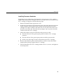
Safety: Before You Remove the Access Cover
Before removing the access cover at any time to work inside the system, observe these
safety guidelines.
1.
Turn off all peripheral devices connected to the system.
2. Turn off the system by using the push-button on/off power switch on the front of
the system.
3. Unplug the AC power cords from the system or wall outlet.
4. Label and disconnect all peripheral cables and all telecommunication lines
connected to I/O connectors or ports on the back of the system.
5. Provide some electrostatic discharge (ESD) protection by wearing an antistatic wrist
strap attached to chassis ground of the system—any unpainted metal surface—
when handling components.
1
Chapter 1: Working Inside the System
Warnings and Cautions
These warnings and cautions apply whenever you remove the access cover of the
system. Only a technically qualified person should integrate and configure the system.
Warning: SYSTEM POWER ON/OFF: The on/off button on the front panel DOES NOT
turn off the system AC power. To remove power from system, you must unplug the AC
power cords from the wall outlet or the system.
Hazardous voltage, current, and energy levels are present inside the power supply.
There are no user-serviceable parts inside it; servicing should be done by technically
qualified personnel.
Hazardous electrical conditions may be present on power, telephone, and
communication cables. Turn off the system and disconnect the power cords,
telecommunications systems, networks, and modems attached to the system before
opening it. Otherwise, personal injury or equipment damage can result.
Caution: Electrostatic discharge (ESD) and ESD protection: ESD can damage disk
drives, boards, and other parts. We recommend that you do all procedures in this chapter
only at an ESD-protected workstation. If one is not available, provide some ESD
protection by wearing an antistatic wrist strap attached to chassis groundany
unpainted metal surfaceon your system when handling parts.
Always handle boards carefully. They can be extremely sensitive to ESD. Hold boards
only by their edges. After removing a board from its protective wrapper or from the
system, place it component-side UP on a grounded, static-free surface. If you place the
baseboard on a conductive surface, the battery leads may short out. If they do, this will
result in a loss of CMOS data and will drain the battery. Use a conductive foam pad if
available but NOT the board wrapper. Do not slide board over any surface.
For proper cooling and airflow, always install the chassis access cover before turning on
the system. Operating the system without the cover in place can damage system parts.
2
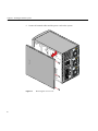
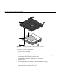
Removing the System Access Cover
Removing the System Access Cover
You need to remove the system access cover, and in some cases the front bezel, to reach
components inside the system. Facing the front of the system, the access cover is on the
right side for pedestal-mounted (tower) servers, and on the top for rack-mounted
servers.
1.
Observe the safety and ESD precautions at the beginning of this chapter.
2. Turn off all peripheral devices connected to the system.
3. If you have not already done so, turn off the system by using the power on/off
switch on the front panel AND unplug all AC power cords.
4. Label and disconnect all peripheral cables attached to the I/O panel on the back of
the system.
5. Remove and save the three screws from the back of the access cover; you will need
them later to reattach the cover.
Note: Be sure the chassis key lock on the front of the system is in the unlocked
position. Otherwise, you will be unable to remove the cover. The chassis keys are not
all the same, you cannot use one key to open multiple units.
6. Place the fingertips of your right hand under the built-in handle on the back of the
cover. A rounded, rectangular depression in the front middle of the access cover
serves as another handle.
7. Using an even pull, slide the cover backward, about an inch, until it stops.
8. Pull the entire cover outward, straight away from the chassis, to disengage the tabs
from the notches in the top and bottom edges of the chassis. Set the cover aside.
Installing the Access Cover
1.
Before replacing the access cover, check that you have not left loose tools or parts
inside the system.
2. Check that cables, PCI option boards, and other components are properly installed.
3. Position the cover over the chassis so that the rows of tabs align with slots in the
chassis. Slide the cover toward the front of the system until the tabs on the cover
firmly engage in the chassis.
4. Attach the cover to the chassis with the three screws you removed earlier, and
tighten them firmly (6.0 inch-pounds).
3
Chapter 1: Working Inside the System
5. Connect all external cables and the power cords to the system.
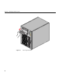
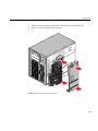
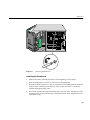
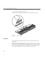
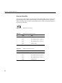
Figure 1-1
4
Removing the Access Cover
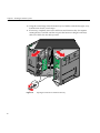
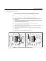
Working in the Subchassis and Electronics Bay
Working in the Subchassis and Electronics Bay
The chassis is comprised of three parts:
•
the main chassis
•
a swing-out subchassis at the front
•
a swing-out subchassis, called the electronics bay, at the rear
To access components in some instances, you must swing away and/or completely
remove the subchassis and electronics bay.
1.
Observe the safety and ESD precautions at the beginning of this chapter.
2. Turn off all peripheral devices connected to the system.
3. Turn off the system power by using the power on/off switch on the front panel
AND unplug all AC power cords.
4. Label and disconnect all peripheral cables attached to the I/O panel on the back of
the system.
5. Remove and save the three screws from the back of the access cover; you will need
them later to reattach the cover.
6. Remove the access cover.
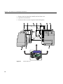
7. Remove the two screws on the top and bottom edges of the chassis (see Figure 1-2).
These screws attach the front subchassis and the electronics bay to the main chassis.
Caution: You must disconnect all cabling to the electronics bay before rotating or
removing the bay. Failure to do so can result in serious damage to system
components. The location of the main connectors in the electronics bay is also shown
in Figure 1-2.
8. Rotate the front subchassis left, away from the main chassis, until it stops.
9. Disconnect and label all cabling to the electronics bay.
5
Chapter 1: Working Inside the System
10. Using the vertical edge of the electronics bay as a handle, rotate the bay right, away
from the main chassis, until it stops.
11. If necessary, completely remove the subchassis and electronics bay: this requires
rotating the bays outward until the two pins that function as hinges for the bays
slide out of their slots. Set the bays aside.
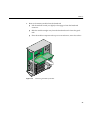
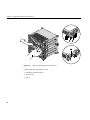
Figure 1-2
6
Opening the Subchassis and Electronics Bay
Installing PCI Boards
Installing PCI Boards
The information in this section covers installation of optional PCI boards.
Caution: Do not overload baseboard: Do not overload the baseboard by installing
optional PCI boards that draw excessive current. Contact your sales or service
representative if you are uncertain that a board is approved for installation in the server.
PCI boards can be extremely sensitive to ESD and always require careful handling. After
removing the board from its protective wrapper or from the baseboard, place it
component-side up on a grounded, static-free surface or conductive foam pad—if
available. Do not slide the board over any surface.
Use the following steps to properly install a PCI option board:
1.
Remove access cover.
2. Remove the PCI option board from its protective wrapper. Be careful not to touch
the components or gold edge connectors. Place board component-side up on an
antistatic surface.
3. Record the serial number of the PCI option board in your equipment log.
4. Set jumpers or switches according to the manufacturer’s instructions.
5. Remove and save the screw that attaches the existing board or expansion slot cover
to the chassis.
6. Remove and save the expansion slot cover.
7. Hold the PCI option board by its top edge or upper corners. Firmly press it into an
expansion slot on the baseboard. The tapered foot of the board retaining bracket
must fit into the mating slot in the expansion slot frame. See Figure 1-3 for an
example.
■
Install an ISA board component-side UP.
■
Install a PCI board component-side DOWN.
8. Use the screw removed earlier to fasten the new board retaining bracket to the
chassis. Tighten the screw firmly (6.0 inch-pounds). Attach cables if necessary.
9. Reinstall the access cover using the original screws.
7
Chapter 1: Working Inside the System
1
2
3
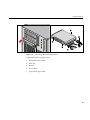
Figure 1-3
Installing a PCI option Board
Components shown in Figure 1-3 are:
1.
PCI or ISA slot
2. Six PCI slots (top to bottom in figure = PCI B4, B3, B2, B1, A3, and A2)
3. PCI slot A1 (Use five inch-length (12.7 cm) board only)
8
Removing a PCI option Board
Removing a PCI option Board
Note: Slot covers must be installed on all vacant expansion slots. This maintains the
electromagnetic emissions characteristics of the system and ensures proper cooling of
system components.
1.
Read and observe the safety and ESD precautions listed at the beginning of this
chapter.
2. Disconnect any cables attached to the board you are removing.
3. Remove and save the screw that attaches the existing board retaining bracket to the
chassis.
4. Holding the board by its top edge or upper corners, carefully pull it out. Do not
scrape the board against other components.
5. Store board in an antistatic protective wrapper.
6. If you are not reinstalling a board in the same slot, install a slot cover over the
vacant slot. The tapered foot of the cover must fit into the mating slot in the
expansion slot frame.
7. Use the screw removed earlier to fasten the new board to the chassis. Tighten the
screw firmly (6.0 inch-pounds).
8. Running the SSU is optional after you remove a PCI or ISA board.
Removing the Front Panel Board
The front panel board contains the system controls and indicators. It is mounted on a
snap-on standoff and a threaded standoff inside the chassis.
1.
Observe the safety and ESD precautions at the beginning of this chapter.
2. Remove the access cover.
3. Disconnect the fan cables and remove the fan housing assembly, see Figure 1-4.
4. Disconnect the 3.5-inch diskette drive cables. Remove the diskette drive carrier from
the chassis. Save the screw to use later.
5. On the front panel board, remove and save the screw from the threaded standoff to
use later.
9
Chapter 1: Working Inside the System
6. Grasp the front panel board. Carefully pull it toward the back of the system until it
pops off the snap-on standoff.
7. Disconnect the front panel board signal cable from the front panel board.
8. Remove the front panel board from the system. Place it on an antistatic foam pad or
a grounded work surface.
Figure 1-4
Removing the Front Panel Board
Installing the Front Panel Board
1.
Reconnect the front panel board signal cable to the front panel board.
2. Position the front panel board over the snap-on standoff and the threaded standoff
inside the chassis.
3. Carefully press the board onto the snap-on standoff until it snaps in place.
4. Reinstall and firmly tighten (6.0 inch-pounds) the screw that secures the board to
the chassis.
5. Reinstall the 3.5-inch diskette drive carrier. Connect the drive cables.
6. Reinstall the access cover using the original screws.
10
Removing the Diskette Drive
Removing the Diskette Drive
1.
Observe the safety and ESD precautions at the beginning of this chapter.
2. Remove the access cover.
3. Disconnect the power and signal cables from the diskette drive. The connectors are
keyed for ease in reconnecting them to the drive, see Figure 1-5.
4. Remove and save the screw that secures the diskette drive carrier to the 5.25-inch
drive bay.
5. Slide the carrier toward the back of the chassis to disengage the tabs from the slots
in the bottom of the 5.25-inch drive bay.
6. Remove the carrier and drive assembly from the chassis, and place it
component-side up on an antistatic surface.
7. Remove the drive from the carrier by sliding the drive forward, toward (and out of)
the front of the carrier. Set the carrier aside.
8. Place the drive in an antistatic protective wrapper if you are not reinstalling the
same drive.
9. Reinstall the access cover using the original screws.
2
3
1
Figure 1-5
Removing the Diskette Drive from the Chassis
11
Chapter 1: Working Inside the System
Components shown in Figure 1-5 are:
1.
Power cable
2. Signal cable
3. Securing screw
Installing the Diskette Drive
1.
Remove the new 3.5-inch diskette drive from its protective wrapper, and place it
component-side up on an antistatic surface. Record the drive model and serial
numbers in your equipment log.
2. Set any jumpers or switches according to the drive manufacturer's instructions.
3. Place the drive carrier on the component-side of the drive.
4. Attach the carrier to the drive by sliding the drive toward the closed/back end of
the carrier. The drive is fully seated when it rests against the square brackets that
form the back of the carrier.
5. Position the carrier so that the two protruding notches fit into the corresponding
slits in the frame. Slide the assembly toward the front of the system to engage the
notches. Make sure the front of the drive fits correctly in the front opening of the
system. When properly positioned, the carrier notches extend slightly into the
interior of the 5.25-inch drive bays and the threaded hole in the carrier aligns with
the threaded hole in the frame.
6. Secure the assembly to the 5.25-inch bay with the screw you removed earlier;
tighten the screw firmly (6.0 inch-pounds).
7. Connect the signal and power cables to the drive. The red stripe on the signal cable
must face toward the center of the drive.
8. Reinstall the access cover using the original screws.
9. Run the SSU to specify that the diskette drive is installed in the system.
12
Peripheral Drives
Peripheral Drives
The following sections provide information on internally mounted drives and cables.
Drive Cabling Considerations
This section summarizes device cabling requirements and constraints. The number of
devices you can install internally depends on:
•
The number supported by the bus
•
The number of physical drive bays available
•
The height of drives in the internal bays (1-inch or 1.6-inch high)
•
The combination of SCSI and IDE devices
IDE Requirements
An 18-inch (45.7 cm) long IDE cable that supports two drives is standard in the system.
If you install an IDE drive, we recommend placing it in the lowest 5.25-inch drive bay to
make cabling easier.
For proper IDE operation, note the cable length specified in Figure 1-6. If no drives are
present on an IDE channel, the cable must be removed. If only one drive is installed, it
must be connected at the end of the cable.
16"
6"
Baseboard
Drive 1
Drive 0
22"
Figure 1-6
IDE Cable Dimensions
Note: If you plan to disable the IDE controller to reuse the interrupt for that controller,
you must physically unplug the IDE cable from the board connector if a cable is present.
Simply disabling the drive by configuring the SSU option does not make the interrupt
available.
13
Chapter 1: Working Inside the System
SCSI Requirements
One narrow and two wide SCSI cables are standard in the system.
All SCSI devices must be unterminated except the peripheral at the end of the SCSI cable.
Hard drives usually provide an active termination, while CD-ROM drives do not.
Because we recommend putting hard drives only in the internal bays, this means that
you should route the SCSI cable so that the last device on the cable is a hard drive in the
internal bay.
Installing 5.25-inch Peripherals in the Front Bays
Three 5.25-inch half-height bays provide space for tape backup, CD-ROM, or other
removable media drives. Note that system EMI integrity and cooling are both protected
by having drives installed in the bays or filler panels and EMI shields covering the bays.
When you install a drive, save the panel and shield to reinstall in case you should later
remove the drive and not reinstall one in the same bay.
To maintain compliance with electromagnetic compatibility (EMC) regulations, the
5.25-inch bays must be configured with either:
•
An EMC-compliant 5.25-inch peripheral device, OR
•
A metal cover plate
Caution: The internal SCSI interface in this system supports only single-ended SCSI
devices on the narrow SCSI channel. Connecting differential SCSI drive types to this
interface can result in electrical damage to the baseboard and peripherals.
We recommend that you do NOT install any hard disk drives in the 5.25-inch bays. The
drives cannot be properly cooled in these locations.
14
Peripheral Drives
It is important that your cabling and connections meet the SCSI bus specification.
Otherwise, the bus could be unreliable and data corruption could occur or devices might
not work at all. The SCSI bus needs to be terminated at the end of the cable; this is usually
provided by the last SCSI device on the cable.
Use the following steps when installing a 5.25-inch peripheral:
1.
Observe the safety and ESD precautions at the beginning of this chapter.
2. Open the front bezel by rotating its right side out and to the left.
Caution: To avoid damage to a 5.25-inch peripheral device, ensure the EMI
gasketing provided in the lower bay does not bridge or short any open circuits of the
exposed peripheral device. If the 5.25-inch device has open circuits, install it in one
of the two upper bays.
3. Put a finger in the hole and pull the EMI metal shield out to disengage it from the
chassis, see Figure 1-7. Save the shield.
4. Remove the drive from its protective wrapper, and place it on an antistatic surface.
5. Record the drive model and serial numbers in your equipment log.
6. Set any jumpers or switches on the drive according to the drive manufacturer’s
instructions.
7. Using two screws of the appropriate size and length (not supplied), attach each
plastic slide rail with its metal grounding plate to the drive, see Figure 1-8.
15
Chapter 1: Working Inside the System
Figure 1-7
16
Removing EMI Shields
Peripheral Drives
4
1
2
Figure 1-8
3
Snap-in Plastic Slide Rails
The components shown in Figure 1-8 are:
1.
Tape drive or other removable media device
2. Tab on slide rail
3. Screws (quantity 4)
4. Slide rails (quantity 2)
Complete the installation of the new 5.25-inch drive using the following steps:
1.
Position the drive so the plastic slide rails engage in the bay guide rails. Push the
drive into the bay until the slide rails lock in place.
2. Connect a power cable to the drive. The connectors are keyed and can be inserted in
only one way.
17
Chapter 1: Working Inside the System
3. Connect a signal cable to the drive. The connectors are keyed and can be inserted in
only one way.
■
SCSI drive: Attach connectors on the cable to the SCSI device or devices you
are installing.
■
IDE drive: The baseboard has one IDE connector. It can support an IDE signal
cable up to 22 inches long. See “Drive Cabling Considerations” on page 13 for
the cable dimensions.
4. Close the front bezel.
Removing a 5.25-inch Peripheral from the Front Bay
1.
Observe the safety and ESD precautions at the beginning of this chapter.
2. Open the front bezel by rotating its right side out and to the left.
3. Disconnect the power and signal cables from the drive.
4. The drive has two protruding plastic, snap-in rails attached. Squeeze the rail tabs
toward each other as you carefully slide the drive forward out of the bay, and place
it on an antistatic surface.
5. Remove and save the four screws and two slide rails.
6. If you leave the bay empty, install a stainless steel EMI shield on the bay for proper
cooling and airflow.
7. If you do not replace the device with another SCSI device, and it was installed at the
end of the SCSI signal cable, modify the cable and termination arrangement so that
a proper termination exists at the end of the cable (it can be a termination device
only, not necessarily a SCSI peripheral).
8. Close the front bezel.
18
Peripheral Drives
1
4
3
2
5
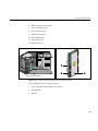
Figure 1-9
Removing a Removable Media Device
Components shown in Figure 1-9 are:
1.
Removable media device
2. Drive rail
3. Rail tab
4. Power cable
5. Typical SCSI signal cable
19
Chapter 1: Working Inside the System
Installing or Replacing the SCSI-B Cable
The cable for channel B has two labels. The channel B cable connects from the SCSI-B
connector on the baseboard to one of the external ports at the back of the server. If you
are uncertain which connector on the baseboard is SCSI B, see Figure 4-1 in Chapter 4,
“Technical Reference.”
Before you install or replace the SCSI-B cable, read and heed all the safety warnings at
the beginning of this chapter. After you shutdown the system, unplug all AC power
cords from the system power supplies or the wall outlets. You may also need to
disconnect all peripheral cables and telecommunication lines connected to I/O
connectors or ports on the back of the system (especially in rackmount units). Use the
following steps to install or replace the cable:
1.
Remove the system access cover and carefully take out the rear foam cover.
2. If desired, you can remove the front foam cover and unscrew and swing out the
front subchassis.
3. Remove the memory module.
4. Remove any existing SCSI-B cable if it is defective or damaged.
5. Attach the new or replacement SCSI-B cable to the SCSI-B connector on the
baseboard. Leave the cable unconnected at the other end.
6. Reinstall the memory module.
7. Remove one of the two knock-out covers, or remove the existing external SCSI-B
connection if installed. See Figure 1-10 at the back of the system. If the server is
upright in pedestal mode, the two covers are at the bottom left, to the left of the I/O
panel.
■
Place the tip of a flat-blade screwdriver, or the end of another suitable tool, in
the slot in the center of the knock-out cover.
■
Rotate, twist, etc., the screwdriver until you free the cover by breaking the small
metal tab that holds the cover to the chassis. Be sure to remove covers that fall
into the chassis.
8. Attach the cable connector to one of the ports at the back of the system as indicated
in Figure 1-10; note where the cable exits the foam and in the expanded detail,
where the cable attaches to one of the ports.
9. Use two screws (included) to secure the connector.
20
Peripheral Drives
10. Reinstall the back foam cover. As you do, position the SCSI cable so that it routes to
the electronics bay through the cutout in the back foam cover. The dotted arrow in
Figure 1-10 shows where the cable must go.
11. Position the cable along the recess in the back foam cover.
12. Reinstall the access cover using the original screws.
13. Connect all AC power and peripheral device cables to the back of the system.
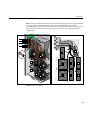
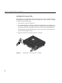
1
2
3
4
5
5
Figure 1-10
6
SCSI-B Cable Installation
21
Chapter 1: Working Inside the System
The components shown in Figure 1-10 are:
1.
SCSI-B connector on the baseboard
2. Rear foam cover
3. Foam tab
4. SCSI-B cable (fit along recess in foam cover)
5. External SCSI-B connection
6. SCSI knockout cover
System Fans
The SGI 1400 server contains eight removable chassis fans that cool the boards and
removable media drives. These chassis fans connect to the front panel board and are
enclosed in a removable foam assembly. The three integrated power supply fan(s)
provide more cooling and airflow.
Removing the System Fan Assembly
Use the following steps and Figure 1-11 to remove the system fan assembly:
1.
Observe the safety and ESD precautions at the beginning this chapter.
2. Remove the access cover.
3. Remove the foam cover from the front subchassis by pulling it straight out.
4. For better access to the individual fan cables on the front panel board, carefully
rotate the right edge of the foam fan assembly outward into the opening where the
foam cover was.
22
System Fans
5. Label and disconnect the individual fan cables from the front panel board.
6. Remove the fan assembly from the chassis.
Figure 1-11
Removing the Fan Assembly
23
Chapter 1: Working Inside the System
Installing the System Fan Assembly
1.
Observe the safety and ESD precautions at the beginning this chapter.
2. Position the fan assembly inside the chassis so that the individual fan cables can
easily reach their connectors on the front panel board.
3. Reconnect the individual fan cables, being careful to match each cable with its
correct connector on the front panel board.
4. Position the fan assembly as it was inside the chassis prior to removal, so that it rests
firmly against the diskette drive at the top and the 5.25-inch bays at the middle and
bottom.
5. Reinstall the foam cover. It is molded to match the position of the fans and fits in
only one way.
6. Reinstall the access cover using the original screws.
Removing an Individual System Fan
Note: Correct airflow direction: The side of each fan is embossed with directional
arrows indicating airflow direction. Always note the direction of the arrows on a fan
before removing it. You will need this information later when you install a different fan.
1.
Observe the safety and ESD precautions at the beginning this chapter.
2. Remove the access cover.
3. Remove the foam cover from the front subchassis by pulling it straight out. Be
careful not to break the foam.
4. For better access to the individual fan cables on the front panel board, carefully
rotate the right edge of the foam fan assembly outward into the opening where the
foam cover was.
5. Label and disconnect the desired fan cable from the front panel board. Be sure to
note the position of the cable where it is held in place in the foam fan assembly.
6. Remove the fan cable from the foam assembly, being careful not to break the foam.
7. Remove the fan from the foam assembly. All systems fans sit differently in the
assembly, but in general, each fan can slide in and out of the foam in only one way.
24
System Fans
Note: The two installed fans nearest the 5.25-inch drive bays (fans 6 and 7) are separated
by a square piece of foam (the piece with a crescent-shaped hole) that extends
perpendicularly from the front of the fans (it is the rectangle between the round faces of
fans 6 and 7). You must remove this piece to access the two fans it separates (pull it
straight out).
1
1
2
2
3
3
4
5
7
4
5
6
6
8
7
8
2
8
8
2
7
5
7
5
1
6
4
3
1
6
4
3
Figure 1-12
Fan Cabling
25
Chapter 1: Working Inside the System
Installing an Individual System Fan
Note: A general rule about correct airflow direction: The removable fan pulls air from
in front of the chassis so that it flows across the boards and out the back. Thus, the fan
must be oriented for the correct airflow direction. In general, the fan’s label is on the side
from which air EXITS the fan. You can confirm correct orientation by checking the
embossed arrows on the side of the fan:
⇒ Arrow points horizontally toward the back of the chassis
• The ⇑ Arrow points vertically up
•
The
Always note the direction of the arrows on the existing fan before you remove it. Replace
a failed fan with the same type as the one removed, with a tachometer signal, or an
approved fan. For a list of approved fans, contact your customer service representative.
1.
See “Removing an Individual System Fan” on page 24, as necessary.
2. Observe the safety and ESD precautions at the beginning this chapter.
3. Slide the fan into its correct receptacle in the foam fan assembly.
4. Attach the cable to the foam at the correct places (when REPLACING a bad fan, you
should have recorded where each cable attaches to the foam).
5. Position the fan assembly inside the chassis so that the individual fan cables can
easily reach their connectors on the front panel board.
6. Attach the cable to the front panel at the correct connector (when REPLACING a
bad fan, you should have recorded where each cable connects to the front panel).
7. Position the fan assembly as it was inside the chassis prior to removal, so that it rests
firmly against the diskette drive at the top and the 5.25-inch bays at the middle and
bottom.
8. Reinstall the foam cover. It is molded to match the position of the fans and fits in
only one way.
9. Reinstall the access cover using the original screws.
26
The Power Share Board
The Power Share Board
The server comes with three power supplies already installed for highest power
availability. If one supply fails, the system can operate using two until a replacement is
installed. Your SGI 1400 system has a power share board (PSB). The PSB supports one to
three supplies.
You can replace an existing power share board by purchasing a kit through your SGI 1400
customer sales or service representative. The following sections describe how to replace
a PSB.
Replacing the Power Share Board (PSB)
1.
Observe the safety and ESD precautions at the beginning this chapter.
2. Label and disconnect all peripheral cables and all telecommunication lines
connected to I/O connectors or ports on the back of the system, and unplug all AC
power cords from the system and wall outlet.
3. Remove all the power supplies, see the SGI 1400 Server Family User’s Guide if
necessary.
4. Remove the access cover.
5. Open the front subchassis.
6. Remove the memory module.
7. Label and disconnect all cables to the baseboard.
8. Remove the electronics bay.
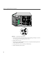
9. Disconnect the cables from the existing power share board (PSB). The board is
behind the electronics bay, see Figure 1-13.
10. Remove and save the two screws (see Figure 1-14) that attach the bracket to the
chassis.
11. To remove the board, lift the BRACKET END first; when you have freed the bracket
from the tabs on the chassis, lift out the entire board.
12. Remove the screws that attach the bracket to the board, see Figure 1-15. Set the
board aside on an antistatic surface or conductive foam pad.
13. Attach the bracket to the new PSB using the correct number of screws.
27
Chapter 1: Working Inside the System
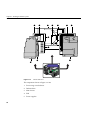
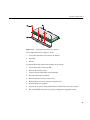
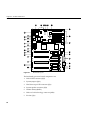
1
2
3
4
5
6
7
8
9
10
11
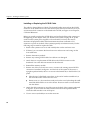
Figure 1-13
Chassis Side View
The components shown in Figure 1-13 are:
1.
Front swing-out subchassis
2. Diskette drive
3. Main chassis
4. PSB
5. Power supplies
28
12
The Power Share Board
6. Baseboard (processor board)
7. Lift-out electronics bay
8. 5.25-inch device bay
9. SCSI hard drive bay
10. Foam fan housing
11. Front foam cover
12. Rear foam cover
3
2
1
Power share board (PSB)
Figure 1-14
Removing the Existing Board and Bracket Assembly
The components shown in Figure 1-14 are:
1.
Screws that attach the bracket to the chassis
2. Existing PSB
3. Bracket
29
Chapter 1: Working Inside the System
2
1
3
Figure 1-15
Removing the Existing Board from its Bracket
The components shown in Figure 1-15 are:
1.
Screws that attach the existing board to the bracket
2. Existing PSB
3. Bracket
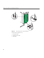
To correctly position the new board inside the chassis:
1.
Insert the NON-BRACKET END, then push the other end down so that the two
slots in the bracket slide over the corresponding tabs on the chassis wall. Figure 1-16
shows an example.
2. Use the two screws you removed earlier to attach the bracket to the chassis.
30
The Power Share Board
2
1
3
Figure 1-16
Attaching the New Board to its Bracket
The components shown in Figure 1-16 are:
1.
Screws that attach the new board to the bracket
2. New PSB
3. Bracket
To reinstall the board and bracket assembly in the chassis:
1.
Connect the cables to the new PSB.
2. Reattach the electronics bay.
3. Connect the new PSB cables to the baseboard.
4. Reconnect the memory module.
5. Reinstall the front and rear foam covers.
6. Reinstall the access cover using the original screws.
7. Reinstall the power supplies.
8. Connect all AC power and peripheral device cables to the rear of the system.
9. Run the FRUSDR load utility to properly configure the upgraded system.
31
Chapter 1: Working Inside the System
3
2
Figure 1-17
1
Installing the New Board and Bracket Assembly
Components shown in Figure 1-17 are:
1.
Two screws that attach the bracket to the chassis
2. Two slots in the bracket that fit over two tabs on the chassis wall
3. Two tabs on the chassis wall that force correct alignment of the board and bracket
assembly
32
Chapter 2
2. Upgrading Baseboard Components
Use the information in this chapter to upgrade or replace components on the system
baseboard (processor board). For information on tools needed, see Chapter 1. For a list of
safety related information see “Safety: Before You Remove the Access Cover” on page 1.
For a complete list of warnings and cautions regarding internal power, ESD, and proper
system cooling, be sure to read “Warnings and Cautions” in Chapter 1.
Caution: Installing or removing jumpers: A jumper is a small, plastic-encased
conductor that slips over two jumper pins. Newer jumpers have a small tab on top that
you can grip with your fingertips or with a pair of fine, needle-nosed pliers. If your
jumpers do not have such a tab, take care when using needle-nosed pliers to remove or
install a jumper; grip the narrow sides of the jumper with the pliers, never the wide sides.
Gripping the wide sides can damage the contacts inside the jumper, causing intermittent
problems with the function controlled by that jumper. Take care to gently grip, but not
squeeze, with the pliers or other tool you use to remove a jumper; you might bend or
break the stake pins on the board.
Baseboard
Use the information in the following sections to remove or install the baseboard.
Removing the Baseboard
Caution: The baseboard can be extremely sensitive to ESD and always requires careful
handling. After removing it from the system, place it component-side UP on a
nonconductive, static-free surface to prevent shorting out the battery leads. If you place
the board on a conductive surface, the battery leads may short out. This will result in a
loss of CMOS data and will drain the battery. Do not slide the baseboard over any
surface.
33
Chapter 2: Upgrading Baseboard Components
1.
Observe the safety and ESD precautions at the beginning of this chapter.
2. Remove the access cover.
3. Remove the front and rear foam covers.
4. Label and disconnect all internal cables connected to add-in boards.
5. Remove all add-in boards.
6. Label and disconnect all internal cables connected to the baseboard.
Note: The baseboard is attached to the electronics bay. In general, the best method for
removing the baseboard is to remove the electronics bay first, particularly in servers
mounted in a pedestal (tower) orientation, though this is not a requirement.
1.
Open the front subchassis and, if necessary, remove the electronics bay.
2. Remove the processors and processor retention module.
3. Remove and save the two screws that secure the baseboard to the chassis.
4. Slide the baseboard toward the front of the server until the board’s I/O connectors
clear the rear of the chassis.
5. See Figure 2-1 for an example of removing the baseboard.
•
The edge of the baseboard at the TOP of the figure (NEAREST and parallel to
the ISA slot) fits into a groove along the edge of the chassis.
•
The edge at the BOTTOM of the figure (OPPOSITE and parallel to the ISA slot)
is free.
6. Place your fingers under the edge of the baseboard OPPOSITE the ISA slot (the edge
at the bottom). Lift the edge a few inches.
7. Slide the baseboard out, toward the edge you just lifted. This will free the opposite
edge (nearest the ISA slot) from the groove that secures it to the chassis.
8. Remove the baseboard and place it component-side up on a nonconductive,
static-free surface or in an antistatic bag.
9. Remove and save the EMI gasket that covers the I/O connectors on the board.
34
Baseboard
Figure 2-1
Removing the Baseboard
Installing the Baseboard
1.
Observe the safety and ESD precautions at the beginning of this chapter.
2. Place the EMI gasket over the I/O connectors on the baseboard.
3. Position the board over the two snap-in standoffs and threaded standoffs inside the
chassis; slide it carefully toward the rear of the system until the I/O connectors
protrude through the back panel.
4. Press the board onto the snap-in standoffs, then insert one screw through one of the
mounting holes of the board and into a threaded standoff. Do not tighten the screw
until the next step.
35
Chapter 2: Upgrading Baseboard Components
5. Insert the remaining screws through the mounting holes and into the threaded
standoffs. Make sure the board is properly seated, then tighten all the screws firmly
(6.0 inch-pounds).
6. Connect all internal cables to the baseboard.
7. Reinstall the add-in boards as applicable.
8. Connect all internal cables to add-in boards.
9. Reinstall the electronics bay if you removed it and close the front subchassis.
10. Reinstall the front and rear foam covers.
11. Reinstall the access cover using the original screws.
12. Connect all peripheral device cables to the I/O panel on the rear of the system.
13. Run the SSU to configure the system.
Memory
Use the following sections to remove or install the memory module or DIMMs.
Removing the Memory Module
Note: Make sure you run the SSU to configure ECC memory. Failure to do so might
degrade the performance of the server.
See the SGI 1400 Server Family User’s Guide if you need more information on memory size
and requirements. Use the following steps to remove a memory module:
1.
Read and observe all safety and ESD precautions listed at the beginning of
Chapter 1.
2. Remove the access cover.
3. Remove the rear foam cover over the electronics bay. It might be easier to do this if
you also remove the front foam cover over the front subchassis, see Figure 2-2.
36
Memory
4. Remove the memory module from the baseboard:
■
Pull the module toward you slightly to disengage it from the baseboard
connector.
■
Slide the module straight away from the baseboard until it clears the guide
rails.
■
Place the module component-side up on a nonconductive, static-free surface.
Figure 2-2
Removing the Memory Module
37
Chapter 2: Upgrading Baseboard Components
Installing the Memory Module
Use the following steps to install or replace a memory module:
1.
Observe the safety and ESD precautions at the beginning of this chapter.
2. Holding the memory module by its edges, align the module so its edge engages in
the guide rail at the back of the electronics bay.
Note: The memory module is held in place by the 242-pin connector on the
baseboard, the guide rail at the back of the electronics bay, and a plastic guide at the
front of the electronics bay. You must support the module until it is fully seated in the
connector.
3. Push the memory module toward the baseboard until it fully engages its connector.
Removing DIMMs
Caution: Use extreme care when removing a DIMM. Too much pressure can damage the
socket slot. Apply only enough pressure on the plastic ejector levers to release the DIMM.
1.
Observe the safety and ESD precautions at the beginning of this chapter.
2. Remove the memory module and place it component-side up on a nonconductive,
static-free surface (see “Removing the Memory Module” on page 36 if you have not
yet done this).
3. Gently push the plastic ejector levers out and down to eject a DIMM from its socket.
4. Hold the DIMM only by its edges, being careful not to touch its components or gold
edge connectors. Carefully lift it away from the socket and store it in an antistatic
package.
5. Repeat to remove other DIMMs as necessary.
•
If you are REPLACING DIMMs, proceed to “Installing DIMMs” on page 39.
•
If you are simply REMOVING DIMMs, continue the procedure with the
following steps.
6. Reinstall the memory module.
7. Reinstall the foam cover(s).
8. Connect all external cables and power cords to the system.
9. Reinstall the access cover using the original screws.
38
Memory
10. Turn on the monitor and then the system.
11. Run the SSU/BIOS Setup to configure the system and to properly set up advanced
memory attributes as required.
Installing DIMMs
DIMMs are keyed and can be inserted in only one way.
Caution: Use extreme care when installing a DIMM. Applying too much pressure can
damage the socket. Mixing dissimilar metals might cause memory failures later,
resulting in data corruption. Install DIMMs with gold-plated edge connectors only in
gold-plated sockets.
Note: DIMM slots on the memory module must be installed only in certain
configurations. See the SGI 1400 Server Family User’s Guide if you are uncertain of the
configuration requirements. Use the following steps to install new DIMMs:
1.
Holding the DIMM only by its edges, remove it from its antistatic package.
2. Orient the DIMM so that the two notches in the bottom edge of the DIMM align
with the keyed socket on the memory module.
3. Insert the bottom edge of the DIMM into the socket, then press down firmly on the
DIMM until it seats correctly.
4. Gently push the plastic ejector levers on the socket ends to the upright position.
5. Repeat the steps to install each DIMM.
6. Reinstall the memory module.
7. Reinstall the foam cover(s).
8. Reinstall the access cover using the original screws.
9. Connect all external cables and the power cords to the system.
39
Chapter 2: Upgrading Baseboard Components
10. Turn on the monitor and then the system.
11. Run the SSU to configure the system and to properly attribute ECC memory.
Figure 2-3
Installing a DIMM
Processors
Use the information in the following sections to remove or install a processor in the
server system.
Caution: Processor must be appropriate: You might damage the system if you install a
processor that is inappropriate for your system. Make sure your system can handle a
newer, faster processor (thermal and power considerations). For exact information about
processor interchangeability, contact your customer service representative.
40
Processors
Reduce the risk of electrostatic discharge (ESD) damage to the processor by doing the
following:
•
Touch the metal chassis before touching the processor or baseboard.
•
Keep part of your body in contact with the metal chassis to dissipate the static
charge while handling the processor.
•
Avoid moving around unnecessarily.
Removing a Processor
1.
Observe the safety and ESD precautions at the beginning of Chapter 1 and the
additional cautions given here.
2. Remove the access cover and the rear foam cover over the electronics bay.
3. As you work, place processors on a grounded, static-free surface or conductive
foam pad.
4. With your right thumb on the face of the retention module bracket, wrap your right
index finger around the tab protruding from the right edge of the bracket. See
Figure 2-4 for an example.
5. Use your index finger to slightly pull the tab outward and to the left. You should not
try to pull the entire bracket; rather, the back of the tab has a latch that releases
when the TAB is pulled slightly.
6. When you have released the right edge of the bracket, rotate it 90° to the left until it
is perpendicular to the front of the retention module. The left edge of the bracket
has an open hinge that can release from the module when you rotate the bracket to
the left.
7. Disengage the open hinge by moving (not rotating) the entire bracket to the right.
Remove the bracket and set it aside.
8. Pull the two tabs attached to the S.E.C. cartridge (see Figure 2-5) straight away from
the baseboard. As you do, the cartridge disengages from its connector on the
baseboard.
9. Slide the S.E.C. cartridge straight away from the baseboard, out of the retention
module. Put it on a piece of conductive foam and store it in an antistatic package.
41
Chapter 2: Upgrading Baseboard Components
2
1
3
Figure 2-4
Releasing the Retention Module Bracket
Components shown in Figure 2-4 are:
1.
Retention module bracket
2. Bracket tab
3. Latch
42
Processors
1
2
3
Figure 2-5
4
Removing a Processor
Components shown in Figure 2-5 are:
1.
An S.E.C. cartridge
2. Retention module guide rails
3. Tabs on the S.E.C. cartridge
4. Processor heat sink
43
Chapter 2: Upgrading Baseboard Components
Installing a Processor
Use Figure 2-6 and the following steps when installing a new or additional processor.
Note: If your system has less than four processors and you are adding one, then you
must remove the termination board in the empty Slot 2 connector. The procedure for
removing a termination board is the same as for removing a processor.
If you plan to reduce the number of processors in your system, then you must replace a
processor with a termination board. The procedure for installing a termination board is
the same for installing a processor.
1.
Read and observe all the safety and ESD precautions at the beginning of Chapter 1.
2. Remove the new processor from its antistatic package and place it on a grounded,
static-free surface or conductive foam pad.
3. Orient the S.E.C. cartridge so that the heat sink faces away from the center of the
baseboard.
If you are installing a termination board, orient it so that the side with the white
bar-code label faces away from the center of the baseboard.
4. With the tabs at the top of the S.E.C. cartridge completely open (pulled outward,
away from the center of the cartridge), slide the cartridge into the guide rails of the
retention module. When done properly, the triangular ends of the tabs (with two
round pegs on each) fit into the entrance to the guide rails.
5. When the cartridge meets resistance, push the two tabs toward each other until the
processor is fully seated.
6. Reattach the retention module bracket:
44
■
With the bracket in an open position (perpendicular to the front of the retention
module), slide the open hinge at the left of the bracket into its receptacle at the
left of the retention module.
■
Rotate the bracket to the right until it reaches the retention module. With your
right thumb on the face of the bracket and your right index finger around the
tab at the right of the bracket, slightly pull the tab outward and to the left to
open the latch at the back of the tab.
■
As you open the latch on the back of the tab, slide the right edge of the bracket
onto the retention module and release the tab. If done correctly, the bracket will
be securely latched.
Processors
7. Reinstall the foam cover.
8. Reinstall the access cover using the original screws.
3
2
Figure 2-6
4
1
Installing a Processor
Figure 2-6 shows the following components:
1.
S.E.C cartridge
2. Retention module guide rails
3. Tabs on the S.E.C. cartridge
4. Processor heat sink (must face away from center of baseboard)
45
Chapter 2: Upgrading Baseboard Components
Installing the Processor Tabs
Depending on your configuration, the tabs for the processor’s S.E.C. cartridge might not
be attached to the cartridge. In this case, you must attach two tabs to each S.E.C. cartridge
as directed in the following steps:
1.
Orient the tab as shown in Figure 2-7.
2. Two small round pegs at the center of the tab correspond with two round holes at
each corner of the S.E.C. cartridge, see Figure 2-7. Spread the tab open slightly to get
the pegs into the holes, being careful not to use too much force and break the tab.
If done properly, the tab will rotate freely with its axis near the center of the tab, at
the base of the triangular section.
3. Repeat to install the second tab to the S.E.C. cartridge.
Figure 2-7
46
Installing Tabs on a Processor S.E.C. Cartridge
Processors
Installing Processor Heatsinks
Depending on your configuration, the heatsink for each processor’s S.E.C. cartridge
might not be attached to the cartridge. In this case, you must attach one heatsink to each
S.E.C. cartridge. Use Figure 2-8 and the following steps:
1.
Remove the heatsink from its protective cover.
2. Pull the tab on the bottom of the heatsink to remove the plastic film and expose the
square of adhesive thermal grease that will help attach the heatsink to the S.E.C.
cartridge. This square is offset, so that more of it is on one side of the center screw
hole than on the other side. This offset side (see Figure 2-8) must point toward the
connector end of the S.E.C. cartridge.
3. Orient the heatsink on the silver metal side of the processor so that:
■
The side with more of the grease square points toward the S.E.C. cartridge
connector
■
The side with less of the grease square points toward the processor tabs
■
All five screw holes align correctly with the holes in the S.E.C. cartridge
4. Because of the adhesive grease on the heatsink, be careful to orient the heatsink
properly before placing it against the S.E.C. cartridge.
5. Attach the heatsink to the S.E.C. cartridge with five 6-32 x 1/4 screws, and tighten to
8-10 inch-pounds.
47
Chapter 2: Upgrading Baseboard Components
1
2
6
7
4
3
5
Figure 2-8
Installing a Heatsink on a Processor S.E.C. Cartridge
The locations shown in Figure 2-8 are:
1.
Processor S.E.C. Cartridge
2. Processor Connector
3. The heatsink edge that goes TOWARD the connector on the S.E.C. cartridge (the
grease square is off-centered toward this edge)
4. Screw hole (five total attach the heatsink to a cartridge)
5. Example screw
6. Grease square (adhesive film must be removed before mounting)
7. Center screw hole: note that the grease square is off-centered from this screw hole
toward the edge (as indicated in callout 3)
48
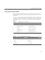
Voltage Regulator Modules (VRMs)
Voltage Regulator Modules (VRMs)
Up to six voltage regulator modules provide power for processors. Every processor
requires 1.5 VRMs, so with four processors, you must use six VRMs. Table 2-1 shows this
relationship.
You must use a specific number and connector population sequence of VRMs for each
combination of processors and termination boards. Table 2-2 lists the required number
and location of VRMs for each potential processor. Figure 2-9 shows this information
graphically.
VRM and Processor Power Sequence
Table 2-1
VRM #
VRM provides power for
Description
1
Processor #1
Processor core power only
2
Processor #1 and #2
L2 cache power only
3
Processor #2
Processor core power only
4
Processor #3
Processor core power only
5
Processor #3 and #4
L2 cache power only
6
Processor #4
Processor core power only
Table 2-2
Processor and VRM Population Sequencing
If you have a processor in connector #
You must have a VRM in connector #
1
1 and 2
1 and 2
1, 2, and 3
1, 2, and 3
1, 2, 3, 4 and 5
1, 2, 3, and 4
1, 2, 3, 4, 5, and 6
49
Chapter 2: Upgrading Baseboard Components
29
1
5
2
6
7
3
8
9
4
10
Figure 2-9
Processor and Corresponding VRM Locations
Components listed in Figure 2-9 are:
1.
Processor connector #4
2. Processor connector #3
3. Processor connector #2
4. Processor connector #1
5. VRM connector #6 (used for processor #4)
6. VRM connector #5 (used for processors #3 and #4)
7. VRM connector #4 (used for processor #3)
8. VRM connector #3 (used for processor #2)
50
Voltage Regulator Modules (VRMs)
9. VRM connector #2 (used for processors #2 and #1)
10. VRM connector #1 (used for processor #1)
Removing a VRM
Use the following information and steps when removing a VRM.
Caution: VRM must be appropriate: You might damage the system if you install a
VRM that is inappropriate for your system. For exact information about VRM and
processor interchangeability, contact your customer service representative.
Note: Reduce the risk of electrostatic discharge (ESD) damage to the VRM by doing the
following:
•
Touch the metal chassis before touching the VRM or baseboard.
•
Keep part of your body in contact with the metal chassis to dissipate the static
charge while handling the VRM.
•
Avoid moving around unnecessarily.
1.
Read and observe the safety and ESD precautions at the beginning of Chapter 1 and
the additional cautions given here.
2. Remove the access cover and the rear foam cover over the electronics bay.
3. As you work, place VRMs on a grounded, static-free surface or conductive foam
pad.
4. Using a small flat-bladed screwdriver, push the plastic ejector levers on each end of
the connector away from the VRM to eject it out of the connector.
5. Place the VRM on a nonconductive, static-free surface, or store it in an antistatic
protective wrapper.
51
Chapter 2: Upgrading Baseboard Components
Installing a VRM
Use Figure 2-10 and the following steps to install a VRM on the system baseboard:
1.
Read and observe the ESD and other warnings listed in the previous section
“Removing a VRM” on page 51.
2. Remove the VRM from its protective package.
3. Carefully insert the VRM in the connector on the baseboard. See Figure 2-10 for an
example.
Note: Make sure you do not bend the connector pins.
4. Push down firmly on both ends of the VRM until the ejector levers of the connector
snap into place, locking the VRM in the connector.
5. Reinstall the rear foam cover over the electronics bay.
6. Reinstall the access cover using the original screws.
1
2
3
Figure 2-10
Installing a VRM
The components shown in Figure 2-10 are:
1.
VRM connector on baseboard
2. VRM
3. Ejector lever
52
Replacing the Backup Battery
Replacing the Backup Battery
The lithium battery on the baseboard (Figure 2-11) powers the real-time clock (RTC) for
three to four years in the absence of power. When the battery weakens, it loses voltage
and the system settings stored in CMOS RAM in the RTC (e.g., the date and time) may
be wrong. Contact your customer service representative or dealer for a list of approved
devices.
Warning: If the system has been running, any installed processor and heat sink on
the processor board(s) will be hot. To avoid the possibility of a burn, be careful when
removing or installing baseboard components that are located near processors.
The following warning and translations of the warning are required by specific certifying
agencies to be printed immediately adjacent to the procedure for removing the RTC.
Warning: There is a danger of explosion if the battery is incorrectly replaced.
Replace only with the same or equivalent type recommended by the equipment
manufacturer. Discard used batteries according to manufacturer’s instructions.
53
Chapter 2: Upgrading Baseboard Components
2
1
3
Figure 2-11
1.
Replacing the Lithium Battery
Observe all the safety and ESD precautions at the beginning of Chapter 1 as well as
the warnings given at the beginning of this section.
2. Remove the access cover.
3. Insert the tip of a small flat-bladed screwdriver or equivalent under the plastic tab
on the snap-on plastic retainer.
4. Gently push down on the screwdriver to lift the battery.
5. Remove the battery from its socket.
54
Replacing the Backup Battery
6. Dispose of the battery according to local ordinance.
7. Remove the new lithium battery from its package and, being careful to observe the
correct polarity, insert it in the battery socket.
8. Reinstall the plastic retainer on the lithium battery socket.
9. Reinstall the access cover using the original screws.
10. Run the SSU to restore the configuration settings to the RTC.
55
Chapter 3
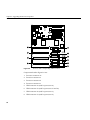
3. SGI 1400 Server SCSI Backplane Installation
SCSI Backplane Warnings and Cautions
The warnings and cautions listed a the beginning of Chapter 1 apply whenever you
remove the access cover of the system. Only a technically qualified person should
perform the upgrade installation described in the following sections. Also see Chapter 1
for a list of tools to use.
Safety: Before You Remove the Access Cover
Before removing the access cover at any time to work inside the system, observe these
safety guidelines.
1.
Turn off all peripheral devices connected to the system.
2. Turn off the system by using the push-button on/off power switch on the front of
the system.
3. Unplug all AC power cords from the system or wall outlet.
4. Label and disconnect all peripheral cables and all telecommunication lines
connected to I/O connectors or ports on the back of the system.
5. Provide some ESD protection by wearing an antistatic wrist strap attached to
chassis ground of the system—any unpainted metal surface—when handling
components.
General Procedure to Open the Chassis
1.
Label and disconnect all peripheral cables and all telecommunication lines
connected to I/O connectors or ports on the back of the system. Unplug all AC
power cords from the system and wall outlet.
2. Remove the access cover, see Figure 3-1.
57
Chapter 3: SGI 1400 Server SCSI Backplane Installation
3. Remove the front foam/fan assembly and rear foam cover.
4. Open the front subchassis.
5. Proceed to the next section to replace the SCSI backplane.
1
2
3
4
5
6
7
8
9
10
11
Figure 3-1
58
Chassis Side View
12
Replacing an Existing Backplane
Components listed in Figure 3-1 are:
1.
Front swing-out subchassis
2. Diskette drive
3. Main chassis
4. Power share board
5. Power supplies
6. Baseboard
7. Lift-out electronics bay
8. 5.25-inch device bay
9. SCSI hard drive bay: backplane mounts to rear of bay
10. Foam cover
11. Foam fan housing
12. Foam fan housing cover
Replacing an Existing Backplane
1.
Remove the existing SCSI hard drive(s) from the hot-docking bay.
Note: If the backplane has optional RAID support you must label and return all
drives to their original locations.
2. Undo the three screws that hold the chassis access cover in place and remove it.
3. Label and disconnect all cables attached to the existing backplane.
4. Remove and save the three screws that attach the upper edge of the backplane to the
chassis.
5. Slide the backplane out from the three clips that attach its lower end to the chassis.
6. Remove the backplane and set it aside on an antistatic surface or conductive foam
pad.
7. Attach the new backplane to the chassis by first sliding the lower end into the three
clips, then using the three screws you removed earlier to attach the upper end.
8. Reconnect cables (removed in step 3) to the new backplane.
59
Chapter 3: SGI 1400 Server SCSI Backplane Installation
9. Replace all screws and covers.
10. Plug all drives back into the bay before powering the system on.
2
1
Figure 3-2
Removing the Backplane from the Chassis
Components shown in Figure 3-2 are:
1.
Attachment screw locations
2. Backplane mounting notches
60
Replacing an Existing Backplane
1
3
2
Figure 3-3
Aligning and Attaching the Backplane
Components shown in Figure 3-3 are:
1.
Backplane mounting notches
2. Backplane SCSI connector
3. Attachment screw locations
61
Chapter 3: SGI 1400 Server SCSI Backplane Installation
1
2
3
Figure 3-4
Reconnecting Cables to the New Backplane
Locations shown in Figure 3-4 are:
1.
Front panel cable
2. Peripheral power cable
3. SCSI Cable
62
General Procedure to Close the Chassis
General Procedure to Close the Chassis
Follow these steps after you have finished the procedure described in the previous
sections.
1.
Close the front subchassis.
2. Reinstall the front and rear foam covers.
3. Reinstall the access cover using the original screws.
4. Reinstall the existing and/or new power supplies.
5. Reconnect all AC power and peripheral device cables to the rear of the system and
to wall outlets.
6. Run the FRUSDR load utility to properly configure the system after adding new
components. See Chapter 3 of the SGI 1400 Server Family User’s Guide.
63
Chapter 4
4. Technical Reference
This section includes:
•
Connectors’ pinouts and baseboard locations
•
Information on baseboard jumpers
•
System I/O Addresses
•
System memory map addresses
•
Baseboard interrupts
•
Video modes
Baseboard Connectors
Figure 4-1 shows connector locations on the baseboard. This section provides pin
information about the connectors.
65
Chapter 4: Technical Reference
1
2
3
4
5
6
7
39
37
38
8
36
35
34
9
33
32
31
30
16
29
28
10
27
11
26
25
17
18
24
19
23
21
Figure 4-1
Baseboard Layout
The baseboard (processor board) components are:
Wide SCSI B connector (J9J1)
2. System jumpers (J6J1)
3. Hard drive input LED connector (J6J3)
4. System speaker connector (J6J2)
5. Lithium battery (B4H1)
6. Wake on LAN technology connector (J4H1)
7. ISA slot (J1J1)
66
13
14
20
22
1.
12
15
Baseboard Connectors
8. PCI slots B4 (closest to ISA), B3, B2, B1, A3, and A2 (farthest from ISA)
9. Memory module connector (J3G1)
10. ICMB connector (J1E1)
11. PCI slot A1 (J2D1)
12. Video and parallel port connectors (J1C1)
13. Serial port connector (J1B2)
14. Keyboard and mouse connectors (J1B1)
15. USB external connector (J1A1)
16. VRM connector for processor 4 (J4E1)
17. VRM connector for processors 4 and 3 (J4C2)
18. VRM connector for processor 3 (J4C1)
19. VRM connector for processor 2 (J4B1)
20. VRM connector for processors 2 and 1 (J4A2)
21. VRM connector for processor 1 (J4A1)
22. Processor 1 Slot 2 connector (J9A1)
23. Main power connector, primary (J9B1)
24. Processor 2 Slot 2 connector (J9B2)
25. Processor 3 Slot 2 connector (J9D1)
26. Main power connector, secondary (J9D2)
27. Front panel connector (J8E1)
28. Processor 4 Slot 2 connector (J9E1)
29. IDE connector (J9E2)
30. Diskette drive connector (J9E3)
31. Auxiliary power connector (J9E4)
32. USB internal header (JC9F14)
33. SMBus connector (J9F2)
34. F16 expansion connector (J7G1)
67
Chapter 4: Technical Reference
35. ITP connector (J6G1)
36. Narrow SCSI connector (J9H1)
37. External IPMB connector (J7H1)
38. SMM connector (J8H1)
39. Wide SCSI A connector (J9H2)
Main Power Connector
Figure 4-2 shows the pins on the main power connector. Table 4-1 lists the pin signal and
color.
1
11
68
10
20
Figure 4-2
Main Power Connector Pins
Table 4-1
Main Power Connector Pinouts
Pin
Signal
Wire Color
1
+3.3 VDC
Orange
2
+3.3 VDC
Orange
3
+3.3 VDC
Orange
4
COM
Black
5
COM
Black
6
COM
Black
7
COM
Black
8
+12 VDC
Yellow
9
+12 VDC
Yellow
10
+12 VDC
Yellow
11
+3.3 VDC
Orange
12
+3.3 VDC
Orange
Baseboard Connectors
Table 4-1 (continued)
Main Power Connector Pinouts
Pin
Signal
Wire Color
13
+3.3 VDC
Orange
14
COM
Black
15
COM
Black
16
COM
Black
17
+5V Standby
Purple
18
+5 VDC
Red
19
+5 VDC
Red
20
+5 VDC
Red
Auxiliary Power
Figure 4-3 shows the auxiliary power connector. Table 4-2 lists the pin number and signal
for each pin.
13
14
1
2
Figure 4-3
Auxiliary Power Connector
Table 4-2
Auxiliary Power Connector Pinouts
Pin
Signal
1
RTN_RS
2
5V_RS
3
3.3V_RS
4
FAN_SPEED
5
I2CSCL
6
I2CSDA
7
GND
69
Chapter 4: Technical Reference
Table 4-2 (continued)
Pin
Signal
8
SYS_PGOOD
9
PS_ON
10
GND
11
-12VCC
12
Key
13
12V_RS
14
GND
Auxiliary Power Connector Pinouts
Diskette Drive
Figure 4-4 shows the diskette drive connector. Table 4-3 lists the diskette drive connector
pinouts.
33
34
70
1
2
Figure 4-4
Diskette Drive Connector
Table 4-3
Diskette Drive Connector Pinouts
Pin
Signal
1
GND
2
FD_DENSEL
3
GND
4
N/C
5
Key
6
FD_DRATE0
7
GND
8
FD_INDEX_L
Baseboard Connectors
Table 4-3 (continued)
Diskette Drive Connector Pinouts
Pin
Signal
9
GND
10
FD_MTR0_L
11
GND
12
FD_DR1_L
13
GND
14
FD_DR0_L
15
GND
16
FD_MTR1_L
17
FD_MSEN1
18
FD_DIR_L
19
GND
20
FD_STEP_L
21
GND
22
FD_WDATA_L
23
GND
24
FD_WGATE_L
25
GND
26
FD_TRK0_L
27
FD_MSEN0
28
FD_WPROT_L
29
GND
30
FD_RDATA_L
31
GND
32
FD_HDSEL_L
71
Chapter 4: Technical Reference
Diskette Drive Connector Pinouts
Table 4-3 (continued)
Pin
Signal
33
GND
34
FD_DSKCHG_L
Front Panel Connector
A 30-pin connector attaches to the chassis front panel containing reset, NMI, sleep, and
power control switches, LED indicators, and IPMB connection. Figure 4-5 shows the
front panel connector. Table 4-4 lists the front panel connector pins and signals.
29
30
72
1
2
Figure 4-5
Front Panel Connector
Table 4-4
Front Panel Connector Pinouts
Pin
Signal
1
SPEAKER_OUT
2
GND
3
CHASSIS_INTRUSI
ON
4
FP_HD_ACT_L
5
+5V
6
SLEEP_CNTRL_l
7
FAN_FAILED_L
8
POWER_LED_L
9
POWER_FAULT_L
10
GND
11
I2C_SDA
Baseboard Connectors
Table 4-4 (continued)
Front Panel Connector Pinouts
Pin
Signal
12
NMI_FP_L
13
I2C_SCL
14
RST_FP_L
15
+5V standby
16
PWR_CNTRL_FP_L
17
FP_ISOL
18
GND
19
FAN_TACH(0)
20
FAN_TACH(1)
21
FAN_TACH(2)
22
FAN_TACH(3)
23
FAN_TACH(4)
24
FAN_TACH(5)
25
FAN_TACH(6)
26
FAN_TACH(7)
27
CLUSTER_LED
28
reserved
29
reserved
30
reserved
73
Chapter 4: Technical Reference
The SMM Connector
Figure 4-6 shows the server management module (SMM) connector. Table 4-5 lists the
SMM connector pinouts.
2
1
74
26
23
Figure 4-6
Server Management Module (SMM) Connector
Table 4-5
Server Management Module Connector Pinouts
Pin
Signal
Description
1
CPU_SMI_L
System Management Interrupt
2
LOCAL_I2C_SCL
IPMB clock line
3
GND
Ground
4
Reserved
N/A
5
PWR_CNTRL_SFC_L
Host power supply on/off control
6
LOCAL_I2C_SDA
IPMB serial data line
7
5VSTNDBY
+5V standby indication (power OK)
8
KEYLOCK_SFC_L
Keyboard lock signal
9
CPU_NMI
Nonmaskable interrupt indication
10
VCC3
3.3V power supply status input
11
RST_SFC_L
Baseboard reset signal from Server Monitor
Module
12
GND
Ground
13
GND
Ground
14
Reserved
N/A
15
SECURE_MODE_BMC
Secure mode indication
16
GND
Ground
17
SFC_CHASSIS_INSTRUSION_L
Chassis intrusion indication
Baseboard Connectors
Table 4-5 (continued)
Server Management Module Connector Pinouts
Pin
Signal
Description
18
Reserved
N/A
19
Reserved
N/A
20
GND
Ground
21
Reserved
N/A
22
Reserved
N/A
23
Reserved
Not used
24
Reserved
N/A
25
Key pin (N/C)
Connector key
26
Reserved
N/A
The IPMB Connector
Figure 4-7 shows the IPMB connector. Table 4-6 lists the IPMB pins and signals.
3
1
2
Figure 4-7
The IPMB Connector
Table 4-6
IPMB Connector Pinouts
Pin
Signal
1
LOCAL_I2C_SCL
2
GND
3
LOCAL_I2C_SDA
75
Chapter 4: Technical Reference
VGA Video Port Connector
Figure 4-8 shows the system’s VGA connector. Table 4-7 lists the pinouts for the VGA
connector.
5
1
10
6
15
76
11
Figure 4-8
VGA Video Port Connector
Table 4-7
Video Port Connector Pinouts
Pin
Signal
1
Red
2
Green
3
Blue
4
N/C
5
GND
6
GND
7
GND
8
GND
10
GND
11
NC
12
DDCDAT
13
HSYNC
14
VSYNC
15
DDCCLK
Baseboard Connectors
Keyboard and Mouse
Figure 4-9 shows the keyboard and mouse connector. Table 4-8 lists the connector
pinouts for the keyboard and mouse connectors.
6
5
4
3
2
1
Figure 4-9
Keyboard and Mouse Connector
The PS/2-compatible connectors share a common housing, but they are functionally
equivalent.
Table 4-8
Keyboard and Mouse Connector Pinouts
Pin
Keyboard signal
Mouse signal
1
KEYDAT
MSEDAT
2
NC
NC
3
GND
GND
4
FUSED_VCC (+5 V)
FUSED_VCC (+5 V)
5
KEYCLK
MSECLK
6
NC
NC
77
Chapter 4: Technical Reference
Parallel Port
Figure 4-10 shows the parallel port connection. Table 4-9 describes the parallel port
connector pin signals.
13
1
25
78
14
Figure 4-10
Parallel Port Connector
Table 4-9
Parallel Port Connector Pinout
Pin
Signal
1
STROBE_L
2
Data bit 0
3
Data bit 1
4
Data bit 2
5
Data bit 3
6
Data bit 4
7
Data bit 5
8
Data bit 6
9
Data bit 7
10
ACK_L
11
Busy
12
PE
13
SLCT
14
AUFDXT_L
15
ERROR_L
Baseboard Connectors
Table 4-9 (continued)
Pin
Signal
16
INIT_L
17
SLCTIN_L
18−25
GND
Parallel Port Connector Pinout
Serial Ports A and B
Figure 4-11 shows the external serial port connector. Table 4-10 lists the serial port
connector pin signals and functional descriptions.
1
5
6
9
Figure 4-11
Serial Port A (External) Connector
Table 4-10
Serial Port A (External) Connector Pinout
Pin
Signal
Description
1
DCD
Data carrier detected
2
RXD
Receive data
3
TXD
Transmit data
4
DTR
Data terminal ready
5
GND
Ground
6
DSR
Data set ready
7
RTS
Request to send
8
CTS
Clear to send
9
RIA
Ring indication active
79
Chapter 4: Technical Reference
Universal Serial Bus
The server provides a single, external Universal Serial Bus (USB) connector at the back
panel (see Figure 4-12) and an internal header to be used with device bay expansion.
Table 4-11 lists the pinouts for the external USB connector. Table 4-12 lists the pinouts for
the internal USB header.
4
1
Figure 4-12
USB External Connector
Table 4-11
USB External Connector Pinout
Pin
Signal
Notes
1
VCC
Cable power
2
Data -
Data (differential pair negative)
3
Data +
Data (differential pair positive)
4
GND
Cable ground
Table 4-12
Pin
USB Internal Header Pinout
Signal
1
80
Notes
N/C
2
Data -
Data (differential pair negative)
3
Data +
Data (differential pair positive)
4
GND
Cable ground
Baseboard Connectors
Narrow SCSI Connector
Figure 4-13 shows the server’s narrow SCSI connector. Table 4-13 lists the narrow SCSI
connection pinouts.
25
1
50
26
Figure 4-13
Narrow SCSI Connector
Table 4-13
Narrow SCSI Connector Pinouts
Pin
Signal
1
GND
2
SCD0_L
3
GND
4
SCD1_L
5
GND
6
SCD2_L
7
GND
8
SCD3_L
9
GND
10
SCD4_L
11
GND
12
SCD5_L
13
GND
14
SCD6_L
15
GND
81
Chapter 4: Technical Reference
Table 4-13 (continued)
82
Pin
Signal
16
SCD7_L
17
GND
18
SCDP_L
19
GND
20
GND
21
GND
22
GND
23
RESERVED
24
RESERVED
25
NC
26
TERMPWR
27
RESERVED
28
RESERVED
29
GND
30
GND
31
GND
32
SATN_L
33
GND
34
GND
35
GND
36
SBSY_L
37
GND
38
SACK_L
39
GND
Narrow SCSI Connector Pinouts
Baseboard Connectors
Table 4-13 (continued)
Pin
Signal
40
SRESET_L
41
GND
42
SMSG_L
43
GND
44
SSEL_L
45
GND
46
SCD_L
47
GND
48
SREQ_L
49
GND
50
SIO_L
Narrow SCSI Connector Pinouts
83
Chapter 4: Technical Reference
Wide SCSI Connector
Figure 4-14 shows the wide SCSI connector. Table 4-14 lists the wide SCSI pinouts and
signal descriptions.
84
34
1
68
35
Figure 4-14
Wide SCSI Connector
Table 4-14
Wide SCSI Connector Pinouts
Pin
Signal
1-16
GND
17
TERMPWR
18
TERMPWR
19
Reserved
20-34
GND
35
DB12_L
36
DB13_L
37
DB14_L
38
DB15_L
39
DBP1_L
40
DB0_L
41
DB1_L
42
DB2_L
43
DB3_L
44
DB4_L
45
DB5_L
Baseboard Connectors
Table 4-14 (continued)
Pin
Signal
46
DB6_L
47
DB7_L
48
DBP _L
49-50
GND
51
TERMPWR
52
TERMPWR
53
Reserved
54
GND
55
ATN_L
56
GND
57
BSY_L
58
ACK_L
59
RST_L
60
MSG_L
61
SEL_L
62
C/D_L
63
REQ_L
64
I/O_L
65
DB8_L
66
DB9_L
67
DB10_L
68
DB11_L
Wide SCSI Connector Pinouts
85
Chapter 4: Technical Reference
Internal IDE Connector
Figure 4-15 shows the server’s internal IDE connector. Table 4-15 lists the connectors and
signals for the internal IDE connector. If no IDE drives are present, no IDE cable should
be connected. If only one IDE drive is installed, it must be connected at the end of the
cable.
39
40
86
1
2
Figure 4-15
Internal IDE Connector
Table 4-15
IDE Connector Pinouts
Pin
Signal
1
RESET_L
2
GND
3
DD7
4
DD8
5
DD6
6
DD9
7
DD5
8
DD10
9
DD4
10
DD11
11
DD3
12
DD12
13
DD2
14
DD13
15
DD1
16
DD14
Baseboard Connectors
Table 4-15 (continued)
IDE Connector Pinouts
Pin
Signal
17
DD0
18
DD15
19
GND
20
Keyed
21
IDEDRQ
22
GND
23
DIOW_L
24
GND
25
DIOR_L
26
GND
27
IORDY
28
CSEL (1 KΩ p/d)
29
IDEDAK_L
30
GND
31
IDEIRQ
32
Reserved (N/C)
33
IDESA1
34
PDIAG_L (tied to
GND)
35
IDESA0
36
IDESA2
37
IDECS1_L
38
IDECS3_L
87
Chapter 4: Technical Reference
Table 4-15 (continued)
Pin
Signal
39
IDEHDACT_L
40
GND
IDE Connector Pinouts
The Hard Drive LED Connector
Figure 4-16 shows the hard drive LED connector. Table 4-16 lists the pins and signals for
the hard drive LED connector.
1
88
4
Figure 4-16
Hard Drive LED Connector
Table 4-16
Hard Drive LED Connector Pinouts
Pin
Signal
1
N/C
2
HD_LED_HDR_L
3
HD_LED_HDR_L
4
N/C
Baseboard Connectors
ISA Connector Pinouts
Table 4-17 lists the ISA connector pinouts and signal names.
Table 4-17
ISA Connector Pinouts
Pin
Signal
A1
IOCHK_L
A2
SD7
A3
SD6
A4
SD5
A5
SD4
A6
SD3
A7
SD2
A8
SD1
A9
SD0
A10
IOCHRDY
A11
AEN
A12
SA19
A13
SA18
A14
SA17
A15
SA16
A16
SA15
A17
SA14
A18
SA13
A19
SA12
A20
SA11
A21
SA10
89
Chapter 4: Technical Reference
Table 4-17 (continued)
90
Pin
Signal
A22
SA9
A23
SA8
A24
SA7
A25
SA6
A26
SA5
A27
SA4
A28
SA3
A29
SA2
A30
SA1
A31
SA0
B1
GND
B2
RESET
B3
+5V
B4
IRQ9
B5
-5V
B6
DRQ2
B7
-12V
B8
SRDY_L
B9
+12V
B10
GND
B11
SMEMW_L
B12
SMEMR_L
B13
IOW_L
B14
IOR_L
ISA Connector Pinouts
Baseboard Connectors
Table 4-17 (continued)
Pin
Signal
B15
DACK3_L
B16
DRQ3
B17
DACK1_L
B18
DRQ1
B19
REFRESH_L
B20
BCLK
B21
IRQ7
B22
IRQ6
B23
IRQ5
B24
IRQ4
B25
IRQ3
B26
DACK2_L
B27
TC
B28
BALE
B29
+5V
B30
OSC
B31
GND
ISA Connector Pinouts
Connector
key
C1
SBHE_L
C2
LA23
C3
LA22
C4
LA21
C5
LA20
91
Chapter 4: Technical Reference
Table 4-17 (continued)
Pin
Signal
C6
LA19
C7
LA18
C8
LA17
C9
MEMR_L
C10
MEMW_L
C11
SD8
C12
SD9
C13
SD10
C14
SD11
C15
SD12
C16
SD13
C17
SD14
C18
SD15
Connector
key
92
D1
MEMCS16_L
D2
IOCS16_L
D3
IRQ10
D4
IRQ11
D5
IRQ12
D6
IRQ15
D7
IRQ14
D8
DACK0_L
D9
DRQ0
ISA Connector Pinouts
Baseboard Connectors
Table 4-17 (continued)
Pin
Signal
D10
DACK5_L
D11
DRQ5
D12
DACK6_L
D13
DRQ6
D14
DACK7_L
D15
DRQ7
D16
+5V
D17
MASTER16_L
D18
GND
ISA Connector Pinouts
The PCI Connectors
Table 4-18 provides the PCI connector pinouts and lists the signal value.
Note: The baseboard does not provide a PCI 3.3 V power connector. Only the 5 V PCI
signaling environment is supported, and no power is available at the 3.3 V signal pins in
expansion slots.
Table 4-18
PCI Connector Pinouts
Pin
Signal
A1
TRST_L
A2
+12 V
A3
TMS
A4
TDI
A5
+5 V
A6
INTA_L
A7
INTC_L
93
Chapter 4: Technical Reference
Table 4-18 (continued)
94
Pin
Signal
A8
+5 V
A9
Reserved
A10
+5 V
A11
Reserved
A12
GND
A13
GND
A14
Reserved
A15
RST_L
A16
+5 V
A17
GNT_L
A18
GND
A19
Reserved
A20
AD30
A21
+3.3 V *
A22
AD28
A23
AD26
A24
GND
A25
AD24
A26
IDSEL
A27
+3.3 V *
A28
AD22
A29
AD20
A30
GND
A31
AD18
PCI Connector Pinouts
Baseboard Connectors
Table 4-18 (continued)
Pin
Signal
A32
AD16
A33
+3.3 V *
A34
FRAME_L
A35
GND
A36
TRDY_L
A37
GND
A38
STOP_L
A39
+3.3 V *
A40
SDONE
A41
SBO_L
A42
GND
A43
PAR
A44
AD15
A45
+3.3 V *
A46
AD13
A47
AD11
A48
GND
A49
AD9
A50
KEY
A51
KEY
A52
C/BE0_L
A53
+3.3 V *
A54
AD6
A55
AD4
PCI Connector Pinouts
95
Chapter 4: Technical Reference
Table 4-18 (continued)
96
Pin
Signal
A56
GND
A57
AD2
A58
AD0
A59
+5 V
A60
REQ64_L
A61
+5 V
A62
+5 V
B1
-12 V
B2
TCK
B3
GND
B4
TD0 (NC)
B5
+5 V
B6
+5 V
B7
INTB_L
B8
INTD_L
B9
PRSNT1_L
B10
Reserved
B11
PRSNT2_L
B12
GND
B13
GND
B14
Reserved
B15
GND
B16
PCICLK
B17
GND
PCI Connector Pinouts
Baseboard Connectors
Table 4-18 (continued)
Pin
Signal
B18
REQ_L
B19
+5 V
B20
AD31
B21
AD29
B22
GND
B23
AD27
B24
AD25
B25
+3.3 V *
B26
C/BE3_L
B27
AD23
B28
GND
B29
AD21
B30
AD19
B31
+3.3 V *
B32
AD17
B33
C/BE2_L
B34
GND
B35
IRDY_L
B36
+3.3 V *
B37
DEVSEL_L
B38
GND
B39
LOCK_L
B40
PERR_L
B41
+3.3 V *
PCI Connector Pinouts
97
Chapter 4: Technical Reference
Table 4-18 (continued)
98
Pin
Signal
B42
SERR_L
B43
+3.3 V *
B44
C/BE1_L
B45
AD14
B46
GND
B47
AD12
B48
AD10
B49
GND
B50
KEY
B51
KEY
B52
AD8
B53
AD7
B54
+3.3 V *
B55
AD5
B56
AD3
B57
GND
B58
AD1
B59
+5 V
B60
ACK64_L
B61
+5 V
B62
+5 V
PCI Connector Pinouts
Baseboard Jumpers
Baseboard Jumpers
One 11-pin single inline header provides three 3-pin jumper blocks that control various
configuration options. Figure 4-17 shows the location. Items shown in bold in Table 4-19
show default placement for each configurable option.
J6J1
11
Figure 4-17
7
3
1
Baseboard Jumpers
99
Chapter 4: Technical Reference
Table 4-19
Baseboard Jumper Summary
Function
Pins (default in bold)
What it does at system reset
CMOS clear
1-2, BMC Control
Preserves the contents of NVRAM.
2-3, Force Erase
Replaces the contents of NVRAM with the
manufacturing default settings.
5-6, Protect
Maintains the current system password.
6-7, Erase
Clears the password.
9-10, Normal
System attempts to boot using the BIOS stored in
flash memory.
10-11, Recovery
BIOS attempts a recovery boot, loading BIOS code
from a diskette into the flash device. This is
typically used when the BIOS code has been
corrupted.
Password clear
Recovery Boot
General Procedure to Change a Jumper Setting
The short general procedure for changing a configuration setting is the same for most of
the jumper functions, and is described in the following steps.
1.
Read and observe the safety and ESD precautions at the beginning of Chapter 1.
2. Turn off all connected peripherals, turn off system power, and disconnect all AC
power cords.
3. Remove the access cover. You do not need to remove the baseboard from the chassis,
and you probably do not need to remove any add-in boards.
4. Locate the configuration jumpers at the edge of the baseboard toward the front of
the system, near the narrow SCSI connector.
5. Move jumper to pins specified for the desired setting.
6. Reinstall the access cover using the original screws, connect the power cords, and
turn on the system for the change to take effect.
7. You may need to repeat these steps to move the jumper back to its original setting,
depending on the jumper function.
100
Baseboard Jumpers
CMOS Clear Jumper
The jumper at pins 1, 2, and 3 controls whether settings stored in CMOS nonvolatile
memory (NVRAM) are retained during a system reset.
Procedure to restore the system’s CMOS and RTC to default values:
1.
See “General Procedure to Change a Jumper Setting” on page 100.
2. Move the CMOS jumper from pins 1 and 2 to pins 2 and 3 (the Clear CMOS memory
position).
3. Reinstall the access cover for your safety (using the original screws), and connect
the power cords to the system.
4. Turn the system on. Wait for POST to complete and for the messages “NVRAM
cleared by jumper” and “Press F2 to enter Setup” to appear. This automatically
reprograms CMOS and RTC to their default settings, except for the password.
5. Enter Setup and make any changes necessary (for example, changing the boot
device). Press F10 to save the new Setup configuration and exit Setup.
6. Turn off the system, and disconnect all AC power cords from the system.
7. Again remove the access cover.
8. Move the jumper from pins 2 and 3 back to pins 1 and 2 (the Protect CMOS memory
position).
9. Reinstall the access cover using the original screws, and connect the power cords to
the system.
10. Run BIOS Setup or the SSU to verify the correct settings. See Chapter 3 in the
SGI 1400 Server Family User’s Guide.
Password Clear Jumper
The jumper at pins 5, 6, and 7 controls whether a stored password is retained or cleared
during a system reset.
Procedure to clear the current password and then enter a new one:
1.
See “General Procedure to Change a Jumper Setting” on page 100.
2. Move the Password jumper from pins 5 and 6 to pins 6 and 7.
101
Chapter 4: Technical Reference
3. Reinstall the access cover for your safety (using the original screws), and connect
the power cords to the system.
4. Turn the system on, and wait for POST to complete. This automatically clears the
password.
5. Turn off the system, and disconnect all AC power cords.
6. Again remove the access cover.
7. Move the jumper from pins 6 and 7 back to pins 5 and 6.
8. Reinstall the access cover using the original screws, and connect the power cords to
the system.
9. Run the SSU to specify a new password. See Chapter 3 in the SGI 1400 Server Family
User’s Guide.
Recovery Boot Jumper
The jumper at pins 9, 10, and 11 controls whether the system attempts to boot using the
BIOS programmed in flash memory.
The following steps disable recovery booting:
1.
See “General Procedure to Change a Jumper Setting” on page 100.
2. Move the recovery boot jumper from pins 9 and 10 to pins 10 and 11.
3. Reinstall the access cover for your safety (using the original screws), then connect
the power cords to the system.
4. Turn the system on, and insert the Flash Memory Update Utility diskette in drive A.
After the system boots, the speaker emits a single beep and the recovery process
starts. This takes about three minutes. When the recovery process completes, the
speaker emits two beeps.
102
Baseboard Jumpers
While in the recovery mode, there is no screen display on the monitor. The keyboard is
disabled as the system automatically recovers the BIOS. The beep codes listed in
Table 4-20 describe the recovery status.
Table 4-20
BIOS Recovery Beep Codes
Beep Code
Message
2
Successful completion, no errors.
4
The system could not boot from the diskette. The diskette may not be
bootable.
Continuous series of low The wrong BIOS recovery files are being used and/or the flash
beeps
memory jumper is in the wrong position.
1.
Turn the system off, disconnect all AC power cords from the system, and remove
the access cover.
2. Move the jumper from pins 10 and 11 back to pins 9 and 10 to enable the normal
boot mode.
3. Replace the access cover, remove the diskette from drive A, and connect the power
cords to the system.
4. After running the special recovery mode, run the SSU to specify a new password.
See Chapter 3 in the SGI 1400 Server Family User’s Guide.
103
Chapter 4: Technical Reference
System I/O Addresses
Table 4-21 shows the location in I/O space of all directly I/O-accessible registers.
Table 4-21
System I/O Addresses
Address(es)
Resource
Device
Notes
0000h - 000Fh
DMA Controller 1
PIIX4E
0010h - 001Fh
DMA Controller 1
PIIX4E
0020h - 0021h
Interrupt Controller 1
PIIX4E
Interrupt Controller 1
PIIX4E
Aliased from 0020h - 0021h
Interrupt Controller 1
PIIX4E
Aliased from 0020h - 0021h
002Ch - 002Dh
Interrupt Controller 1
PIIX4E
Aliased from 0020h - 0021h
002Eh - 002Fh
Super I/O Index and Data
Ports
0030h - 0031h
Interrupt Controller 1
PIIX4E
Aliased from 0020h - 0021h
Interrupt Controller 1
PIIX4E
Aliased from 0020h - 0021h
Interrupt Controller 1
PIIX4E
Aliased from 0020h - 0021h
Interrupt Controller 1
PIIX4E
Aliased from 0020h - 0021h
Programmable Timers
PIIX4E
Programmable Timers
PIIX4E
Aliased from 0000h - 000Fh
0022h - 0023h
0024h - 0025h
0026h - 0027h
0028h - 0029h
002Ah - 002Bh
0032h - 0033h
0034h - 0035h
0036h - 0037h
0038h - 0039h
003Ah - 003Bh
003Ch - 003Dh
003Eh - 003Fh
0040h - 0043h
0044h - 004Fh
0050h - 0053h
104
Aliased from 0040h - 0043h
System I/O Addresses
Table 4-21 (continued)
Address(es)
System I/O Addresses
Resource
Device
Notes
0054h - 005Fh
0060h, 0064h
Keyboard Controller
Keyboard chip select from 87307
0061h
NMI Status & Control
Register
PIIX4E
0063h
NMI Status & Control
Register
PIIX4E
Aliased
0065h
NMI Status & Control
Register
PIIX4E
Aliased
0067h
NMI Status & Control
Register
PIIX4E
Aliased
0070h
NMI Mask (bit 7) & RTC
Address (bits 6::0)
PIIX4E
0072h
NMI Mask (bit 7) & RTC
Address (bits 6::0)
PIIX4E
Aliased from 0070h
0074h
NMI Mask (bit 7) & RTC
Address (bits 6::0)
PIIX4E
Aliased from 0070h
0076h
NMI Mask (bit 7) & RTC
Address (bits 6::0)
PIIX4E
Aliased from 0070h
0071h
RTC Data
PIIX4E
0073h
RTC Data
PIIX4E
Aliased from 0071h
0075h
RTC Data
PIIX4E
Aliased from 0071h
0077h
RTC Data
PIIX4E
Aliased from 0071h
0080h - 008Fh
DMA Low Page Register
PIIX4E
0090h - 0091h
DMA Low Page Register
(aliased)
PIIX4E
0092h
System Control Port A
(PC-AT control Port) (this
port not aliased in DMA
range)
PIIX4E
105
Chapter 4: Technical Reference
Table 4-21 (continued)
106
System I/O Addresses
Address(es)
Resource
Device
0093h - 009Fh
DMA Low Page Register
(aliased)
PIIX4E
0094h
Video Display Controller
00A0h - 00A1h
Interrupt Controller 2
PIIX4E
00A4h - 00A15
Interrupt Controller 2
(aliased)
PIIX4E
00A8h - 00A19
Interrupt Controller 2
(aliased)
PIIX4E
00Ach - 00Adh
Interrupt Controller 2
(aliased)
PIIX4E
00B0h - 00B1h
Interrupt Controller 2
(aliased)
PIIX4E
00B2h
Advanced Power
Management Control
PIIX4E
00B3h
Advanced Power
Management Status
PIIX4E
00B4h - 00B5h
Interrupt Controller 2
(aliased)
PIIX4E
00B8h - 00B9h
Interrupt Controller 2
(aliased)
PIIX4E
00BCh - 00BDh
Interrupt Controller 2
(aliased)
PIIX4E
00C0h - 00DFh
DMA Controller 2
PIIX4E
00F0h
Clear NPX error
00F8h - 00FFh
x87 Numeric Coprocessor
0102h
Video Display Controller
0170h - 0177h
Secondary Fixed Disk
Controller (IDE)
Notes
Resets IRQ13
PIIX4E
Not used
System I/O Addresses
Table 4-21 (continued)
System I/O Addresses
Address(es)
Resource
Device
01F0h - 01F7h
Primary Fixed Disk
Controller (IDE)
PIIX4E
0200h - 0207h
Game I/O Port
0220h - 022Fh
Serial Port A
0238h - 023Fh
Serial Port B
0278h - 027Fh
Parallel Port 3
02E8h - 02Efh
Serial Port B
02F8h - 02FFh
Serial Port B
0338h - 033Fh
Serial Port B
0370h - 0375h
Secondary Diskette
0376h
Secondary IDE
0377h
Secondary IDE/Diskette
0378h - 037Fh
Parallel Port 2
03B4h - 03Bah
Monochrome Display Port
03BCh - 03BFh
Parallel Port 1 (Primary)
03C0h - 03CFh
Video Display Controller
03D4h - 03DAh
Color Graphics Controller
03E8h - 03EFh
Serial Port A
03F0h - 03F5h
Diskette Controller
03F6h - 03F7h
Primary IDE - Sec. Diskette
03F8h - 03FFh
Serial Port A (Primary)
0400h - 043Fh
DMA Controller 1, Extended PIIX4E
Mode Registers
04D0h - 04D1h
Interrupt Controllers 1 and 2
Control Register
Notes
Not used
107
Chapter 4: Technical Reference
Table 4-21 (continued)
System I/O Addresses
Address(es)
Resource
Device
0678h - 067Ah
Parallel Port (ECP)
0778h - 077Ah
Parallel Port (ECP)
07BCh - 07BEh
Parallel Port (ECP)
0CA0 - CA3h
BMC Registers
0CF8h
PCI CONFIG_ADDRESS
Register
0CF9h
NBX Turbo and Reset
control
0CFCh
PCI CONFIG_DATA
Register
46E8h
Video Display Controller
Notes
Located in 450NX
PIIX4E
Located in 450NX
Memory Map Address Range
Table 4-22 lists the memory map address ranges and the functions they support.
Table 4-22
108
Memory Map Address Range
Address Range (hex)
Amount
Function
0 to 07FFFFh
640 KB
DOS region, base system memory
0A0000h to 0BFFFFh
128 KB
Video or SMM memory
0C0000h and 0DFFFFh
128 KB
Add-in board BIOS and buffer area
0E0000h to 0FFFFFh
128 KB
System BIOS
0E0000h to 0EFFFFh
2 MB
Extended system BIOS
FC000000h to FFFFFFFFh
64 MB
PCI memory space
Interrupts
Interrupts
Table 4-23 recommends the logical interrupt mapping of interrupt sources; it reflects a
typical configuration, but these interrupts can be changed by the user. Use the
information to determine how to program each interrupt. The actual interrupt map is
defined using configuration registers in the PIIX4E and the I/O controller. I/O
Redirection Registers in the I/O APIC are provided for each interrupt signal; the signals
define hardware interrupt signal characteristics for APIC messages sent to local APIC(s).
Note: To disable either IDE controller and reuse the interrupt: if you plan to disable
either IDE controller to reuse the interrupt for that controller, you must physically
unplug the IDE cable from the board connector (IDE0) if a cable is present. Simply
disabling the drive by configuring the SSU option does not make the interrupt available.
Table 4-23
Interrupt I/O Descriptions
Interrupt
I/O APIC level
Description
INTR
INT0
Processor interrupt
NMI
N/A
NMI from PIC to processor
IRQ1
INT1
Keyboard interrupt
Cascade
INT2
Interrupt signal from second 8259 in PIIX4E
IRQ3
INT3
Serial port A or B interrupt from SIO device (user can
configure)
IRQ4
INT4
Serial port A or B interrupt from SIO device (user can
configure)
IRQ5
INT5
Parallel port II
IRQ6
INT6
Diskette port
IRQ7
INT7
Parallel port
IRQ8_L
INT8
RTC interrupt
IRQ9
INT9
Signal control interrupt (SCI) used by ACPI-compliant
OS
IRQ10
INT10
IRQ11
INT11
109
Chapter 4: Technical Reference
Table 4-23 (continued)
Interrupt I/O Descriptions
Interrupt
I/O APIC level
Description
IRQ12
INT12
Mouse interrupt
INT13
IRQ14
INT14
IRQ15
INT15
SMI_L
Compatibility IDE interrupt from primary channel IDE
devices 0 and 1
System management interrupt—general purpose
indicator sourced by the PIIX4E and BMC through the
PID to the processors
Video Modes
The CL-GD5480 integrated video controller provides all standard IBM VGA modes. With
2 MB of SGRAM standard, the system supports special Cirrus Logic extended modes.
Table 4-24 and Table 4-25 list the standard and extended modes that this implementation
supports, including the number of colors and palette size (e.g., 16 colors out of 256 K
colors), resolution, pixel frequency, and scan frequencies.
Standard VGA Modes
Table 4-24
110
Mode(s)
in Hex
Bits per
pixel
Colors (no per
palette size)
Resolution
Pixel Freq.
(MHz)
Horizontal
Freq. (kHz)
Vertical Freq.
(Hz)
0, 1
4
16/256K
360 X 400
14
31.5
70
2, 3
4
16/256K
720 X 400
28
31.5
70
4, 5
4
4/256K
320 X 200
12.5
31.5
70
6
4
2/256K
640 X 200
25
31.5
70
7
4
Mono
720 X 400
28
31.5
70
D
4
16/256K
320 X 200
12.5
31.5
70
E
4
16/256K
640 X 200
25
31.5
70
F
4
Mono
640 X 350
25
31.5
70
Video Modes
Table 4-24 (continued)
Standard VGA Modes
Mode(s)
in Hex
Bits per
pixel
Colors (no per
palette size)
Resolution
Pixel Freq.
(MHz)
Horizontal
Freq. (kHz)
Vertical Freq.
(Hz)
10
4
16/256K
640 X 350
25
31.5
70
11
4
2/256K
640 X 480
25
31.5
60
12
4
16/256K
640 X 480
25
31.5
60
12+
4
16/256K
640 X 480
31.5
37.5
75
13
8
256/256K
320 X 200
12.5
31.5
70
Extended VGA Modes
Table 4-25
Mode(s)
in Hex
Bits per
pixel
Colors
Resolution
Pixel Freq.
(MHz)
Horiz. Freq.
(KHz)
Vert. Freq.
(Hz)
Memory
58, 6A
8
16/256K
800 X 600
36
35.2
56
1MB
58, 6A
8
16/256K
800 X 600
40
37.8
60
1MB
58, 6A
8
16/256K
800 X 600
50
48.1
72
1MB
58, 6A
8
16/256K
800 X 600
49.5
46.9
75
1MB
5C
8
256/256K
800 X 600
36
35.2
56
1MB
5C
8
256/256K
800 X 600
40
37.9
60
1MB
5C
8
256/256K
800 X 600
50
48.1
72
1MB
5C
8
256/256K
800 X 600
49.5
46.9
75
1MB
5C
8
256/256K
800 X 600
56.25
53.7
85
1MB
5C
8
256/256K
800 X 600
68.2
63.6
100
1MB
5D
8
16/256K
1024 X 768
(interlaced)
44.9
35.5
43
1MB
5D
8
16/256K
1024 X 768
65
48.3
60
1MB
5D
8
16/256K
1024 X 768
75
56
70
1MB
111
Chapter 4: Technical Reference
Table 4-25 (continued)
112
Extended VGA Modes
Mode(s)
in Hex
Bits per
pixel
Colors
Resolution
Pixel Freq.
(MHz)
Horiz. Freq.
(KHz)
Vert. Freq.
(Hz)
Memory
5D
8
16/256K
1024 X 768
78.7
60
75
1MB
5E
8
256/256K
640 X 400
25
31.5
70
1MB
5F
8
256/256K
640 X 480
25
31.5
60
1MB
5F
8
256/256K
640 X 480
31.5
37.9
72
1MB
5F
8
256/256K
640 X 480
31.5
37.5
75
1MB
5F
8
256/256K
640 X 480
36
43.3
85
1MB
5F
8
256/256K
640 X 480
43.2
50.9
100
1MB
60
8
256/256K
1024 X 768
(interlaced)
44.9
35.5
43
1MB
60
8
256/256K
1024 X 768
65
48.3
60
1MB
60
8
256/256K
1024 X 768
75
56
70
1MB
60
8
256/256K
1024 X 768
78.7
60
75
1MB
60
8
256/256K
1024 X 768
94.5
68.3
85
1MB
60
8
256/256K
1024 X 768
113.3
81.4
100
1MB
64
16
64K
640 X 480
25
31.5
60
1MB
64
16
64K
640 X 480
31.5
37.9
72
1MB
64
16
64K
640 X 480
31.5
37.5
75
1MB
64
16
64K
640 X 480
36
43.3
85
1MB
64
16
64K
640 X 480
43.2
50.9
100
1MB
65
16
64K
800 X 600
36
35.2
56
1MB
65
16
64K
800 X 600
40
37.8
60
1MB
65
16
64K
800 X 600
50
48.1
72
1MB
65
16
64K
800 X 600
49.5
46.9
75
1MB
65
16
64K
800 X 600
56.25
53.7
85
1MB
Video Modes
Table 4-25 (continued)
Extended VGA Modes
Mode(s)
in Hex
Bits per
pixel
Colors
Resolution
Pixel Freq.
(MHz)
Horiz. Freq.
(KHz)
Vert. Freq.
(Hz)
Memory
65
16
64K
800 X 600
68.2
63.6
100
1MB
66
16
32K
640 X 480
25
31.5
60
1MB
66
16
32K
640 X 480
31.5
37.9
72
1MB
66
16
32K
640 X 480
31.5
37.5
75
1MB
66
16
32K
640 X 480
36
43.3
85
1MB
66
16
32K
640 X 480
43.2
50.9
100
1MB
67
16
32K
800 X 600
36
35.2
56
1MB
67
16
32K
800 X 600
40
37.8
60
1MB
67
16
32K
800 X 600
50
48.1
72
1MB
67
16
32K
800 X 600
49.5
46.9
75
1MB
67
16
32K
800 X 600
56.25
53.7
85
1MB
67
16
32K
800 X 600
68.2
63.6
100
1MB
68
16
32K
1024 X 768
(interlaced)
44.9
35.5
43
2MB
68
16
32K
1024 X 768
65
48.3
60
2MB
68
16
32K
1024 X 768
75
56
70
2MB
68
16
32K
1024 X 768
78.7
60
75
2MB
68
16
32K
1024 X 768
94.5
68.3
85
2MB
68
16
32K
1024 X 768
113.3
81.4
100
2MB
6C
8
16/256K
1280 X 1024 75
(interlaced)
48
43
1MB
6D
8
256/256K
1280 X 1024 75
(interlaced)
48
43
2MB
6D
8
256/256K
1280 X 1024 108
65
60
2MB
6D
8
256/256K
1280 X 1024 135
80
75
2MB
113
Table 4-25 (continued)
Extended VGA Modes
Mode(s)
in Hex
Bits per
pixel
Colors
Resolution
6D
8
256/256K
6E
16
6E
Pixel Freq.
(MHz)
Horiz. Freq.
(KHz)
Vert. Freq.
(Hz)
Memory
1280 X 1024 157.5
91
85
2MB
32K
1152 X 864
94.5
63.9
70
2MB
16
32K
1152 X 864
108
67.5
75
2MB
6E
16
32K
1152 X 864
121.5
76.7
85
2MB
6E
16
32K
1152 X 864
143.5
91.5
100
2MB
71
24
16M
640 X 480
25
31.5
60
1MB
71
24
16M
640 X 480
31.5
37.9
72
1MB
71
24
16M
640 X 480
31.5
37.5
75
1MB
71
24
16M
640 X 480
36
43.3
85
1MB
71
24
16M
640 X 480
43.2
50.9
100
1MB
74
16
64K
1024 X 768
(interlaced)
44.9
35.5
43
2MB
74
16
64K
1024 X 768
65
48.3
60
2MB
74
16
64K
1024 X 768
75
56
70
2MB
74
16
64K
1024 X 768
78.7
60
75
2MB
74
16
64K
1024 X 768
94.5
68.3
85
2MB
74
16
64K
1024 X 768
113.3
81.4
100
2MB
78
16
32K
800 X 600
36
35.2
56
1MB
78
24
16M
800 X 600
40
37.8
60
2MB
78
24
16M
800 X 600
50
48.1
72
2MB
78
24
16M
800 X 600
49.5
46.9
75
2MB
78
24
16M
800 X 600
56.25
53.7
85
2MB
78
24
16M
800 X 600
68.2
63.6
100
2MB
Video Modes
Table 4-25 (continued)
Mode(s)
in Hex
Bits per
pixel
Colors
7B
8
7B
Extended VGA Modes
Resolution
Pixel Freq.
(MHz)
Horiz. Freq.
(KHz)
Vert. Freq.
(Hz)
Memory
256/256K
1600 X 1200 135
(interlaced)
62.5
48
2MB
8
256/256K
1600 X 1200 162
75
60
2MB
7C
8
256/256K
1152 X 864
94.5
63.9
70
1MB
7C
8
256/256K
1152 X 864
108
67.5
75
1MB
7C
8
256/256K
1152 X 864
121.5
76.7
85
1MB
7C
8
256/256K
1152 X 864
143.5
91.5
100
1MB
7D
16
64K
1152 X 864
94.5
63.9
70
2MB
7D
16
64K
1152 X 864
108
67.5
75
2MB
7D
16
64K
1152 X 864
121.5
76.7
85
2MB
7D
16
64K
1152 X 864
143.5
91.5
100
2MB
115
Appendix A
A. Equipment Log and Configuration Worksheets
Equipment Log
Use the blank equipment log provided here (Table A-1) to record information about your
system. You will need some of this information when you run the SSU.
Table A-1
Item
Equipment Log
Manufacturer Name and Model Number
Serial Number
Date Installed
System
Baseboard
Processor speed and cache
Video display
Keyboard
Mouse
Diskette drive A
Diskette drive B
Tape drive
CD-ROM drive
117
Appendix A: Equipment Log and Configuration Worksheets
Table A-1 (continued)
Item
Hard disk drive 1
Hard disk drive 2
Hard disk drive 3
Hard disk drive 4
Hard disk drive 5
SCSI host adapter board 1
118
Equipment Log
Manufacturer Name and Model Number
Serial Number
Date Installed
Equipment Log
Table A-1 (continued)
Item
Equipment Log
Manufacturer Name and Model Number
Serial Number
Date Installed
119
Appendix A: Equipment Log and Configuration Worksheets
Configuration Worksheets
The rest of this chapter consists of worksheets to record the settings you make when
configuring the system using the SSU, BIOS Setup, and the Symbios SCSI Utility. If
default values ever need to be restored to CMOS (e.g., after a CMOS-clear), you must
reconfigure the system. Referring to the filled-in worksheets could make your task easier.
Circle or write in your selections or the values that are displayed onscreen.
Current Usage
As all SGI 1400 servers come equipped with three power supplies standard, power usage
is not generally a critical consideration. The system administrator or service person may
wish to calculate system power usage for other reasons.
As an overall current usage limitation on the power supply, do not exceed a combined
power output of 195 watts for the +5 and +3.3 volt outputs.
Calculating Power Usage
The total combined wattage for the system configuration must be less than 400 watts.
Use the two worksheets in this section to calculate the total used by your system. For
current and voltage requirements of add-in boards and peripherals, see your vendor
documents.
120
Current Usage
Worksheet, Calculating DC Power Usage
1.
List the current for each board and device in the appropriate voltage level column of
Table A-2.
2. Add the currents in each column. Then go to the next worksheet.
Table A-2
Power Usage Worksheet
Device, by Current (maximum)
at voltage level:
+3.3 V
+5 V
–5 V
+12 V
–12 V
Boards, processors, and memory (get
totals from your board manual)
SCSI backplane
Front panel board
3.5-inch diskette drive
0.3 A
CD-ROM drive
0.4 A
1.0 A
Second 5.25-inch device
1st hot-swap hard drive
2nd hot-swap hard drive
3rd hot-swap hard drive
4th hot-swap hard drive
5th hot-swap hard drive
Cooling fan 1, 120 mm
0.6 A
Cooling fan 2, 120 mm
0.6 A
Cooling fan 3, 120 mm
0.6 A
Total Current
121
Appendix A: Equipment Log and Configuration Worksheets
Worksheet, Total Combined Power Used by the System
1.
From the previous worksheet, enter the total current for each column.
2. Multiply the voltage by the total current to get the total wattage for each voltage
level as indicated in Table A-3.
3. Add the total wattage for each voltage level to arrive at a total combined power
usage on the power supply.
Table A-3
122
Power Usage Worksheet (Total Watts)
Voltage level and total current (V X A = W)
Total Watts for each voltage level
(+3.3 V) X (______ A)
________ W
(+5 V) X (______ A)
________ W
(−5 V) X (______ A)
________ W
(+12 V) X (______ A)
________ W
(–12 V) X (______ A)
________ W
Total Combined Wattage
________ W
System Setup Utility (SSU) Worksheets
System Setup Utility (SSU) Worksheets
This section provides worksheets for tracking changes made using the SSU.
Adding and Removing Boards
Table A-4 provides PCI board information.
Table A-4
Add or Remove PCI Boards
Baseboard
PCI Host Bridge Device
Bus 0 Dev 0
PCI SCSI Device
Bus 0 Dev B
PCI Ethernet Device
Bus 0 Dev 10
PCI VGA Device
Bus 0 Dev 12
PCI Multifunction Device
Bus 0 Dev 14
123
Appendix A: Equipment Log and Configuration Worksheets
ISA Board Definition
If you have an ISA board with no.CFG file, you can define the board by using the SSU. It
is necessary to define an ISA board only when you want to prevent other boards in the
system from using the same IRQ levels, DMA channels, I/O Port addresses, or Memory
addresses that your ISA board uses. Table A-5 provides some ISA board definitions.
Table A-5
ISA Board Definition
(ISA) Board Name
Manufacturer
Board Type
Video Board Memory Board
Multifunction Board Keyboard
Mass Storage Device Numeric Coprocessor
Network Board Operating System
Communications Board CPU Board
Parallel Port Joystick Board
Pointing Device Other
Board Slot
DMA
16 Bit / 8 Bit / 8 or 16 Bit
Channel:
Size: Byte / Word
Timing: Default / Type A / Type B
IRQ
Level:
Trigger: Edge / Level
Ports
ISA Port Definition
Start:
End:
Size: Byte / Word
Memory
ISA Memory Definition
Size: KB
Address: h
RAM / ROM
Don’t Cache / Cache
Use: System / Expanded / Virtual / Other
Width: Byte / Word
Decode: 24 Bit / 20 Bit
124
System Setup Utility (SSU) Worksheets
Baseboard (SSU, Change Configuration Settings)
Table A-6
Systems Group
System Identification and Version Information
SSU Configuration File Version
MP Spec. Version
1.1 / 1.4
Processor Speed Setting
Table A-7
Memory Subsystem Group
Onboard Disk Controllers
Onboard Communication Devices
Table A-8
Enable / Disable
Onboard Disk Controllers
Onboard Diskette Controller
Enable / Disable
Primary Onboard IDE Controller
Enable / Disable
Secondary Onboard IDE Controller
Enable / Disable
125
Appendix A: Equipment Log and Configuration Worksheets
Table A-9
Onboard Communications Devices
Serial Port 1 Configuration
Serial Port 2 Configuration
Serial Port 2 Mode
Parallel Port Configuration
Parallel Port Mode
Table A-10
Diskette Drive Subsystems Group
Diskette drive A Options
Diskette drive B Options
Table A-11
126
IDE Subsystem Group
IDE Configuration
Primary Master
(drive name)
None / User / Auto / CD
IDE Drive Options
Primary Master
2 Sector/Block / 4 Sector/Block 8 Sector/Block / 16 Sector/Block /
Disable
Transfer Mode
Primary Master
PIO 1 / PIO 2 / PIO 3 / PIO 4
IDE Configuration
Primary Slave
(drive name)
None / User / Auto / CD
IDE Drive Options
Primary Slave
2 Sector/Block / 4 Sector/Block / 8 Sector/Block / 16 Sector/Block /
Disable
Translation Mode
Primary Slave
Standard CHS
Logical Block Addressing
Transfer Mode
Primary Slave
PIO 1 / PIO 2 / PIO 3 / PIO 4
System Setup Utility (SSU) Worksheets
Table A-12
Multiboot Group
Boot Device Priority
Table A-13
Diskette Drive
Removable Devices
Hard Drive
ATAPI CD-ROM Drive
Diagnostic Boot
Keyboard and Mouse Subsystem Group
Typematic Delay
250 ms delay / 500 ms delay
750 ms delay / 1000 ms delay
Typematic Speed
30 CPS / (other)
Mouse Control option
Mouse Enabled / Disabled
Table A-14
Console Redirection
COM Port for Redirection
Port 3F8/IRQ4 / Port 2F8/IRQ3
Port 3E8h/IRQ 3 / Disable
Serial Port baud rate
9600 / 19.2k / 38.4k / 115.2k
Hardware Flow Control
None / CTS/RTS / CTS/RTS + CD / Xoff/Xon
Terminal Type
PC - ANSI / VT 100
127
Appendix A: Equipment Log and Configuration Worksheets
Table A-15
Security Subsystems Worksheet
Administrative Password
Disable / Enable
User Password
Disable / Enable
Secure Mode Hot-Key
None / Ctrl-Alt-{
Lockout Timer
Disable / {
Secure Boot Mode
Disable / Enable
Video Blanking
Disable / Enable
Diskette Writes
Disable / Enable
Reset/Power Switch Locking
Disable / Enable
Table A-16
128
} minutes
SCSI ROM BIOS Options Group
Onboard SCSI ROM BIOS scan
Table A-17
}
Enable / Disable
Management Subsystem Group
System Sensor Control
Write your selections on a separate page.
SMM Enable
Enable / Disable
Event Logging
Enable / Disable
PCI System Error Detection
Enable / Disable
System Setup Utility (SSU) Worksheets
Management Subsystem, System Sensor Control Worksheet
For each sensor control, the display includes the choices shown below, with blanks for
entering values. Write in both the sensor control and the values you select. This group of
tabular worksheets provides space for a number of sensor controls; if you need more
space, copy these pages to extend your worksheet.
Table A-18
Sensor Control Values
Item:
Disable / Enable
Upper Fatal:
Upper Warning:
Lower Warning:
Lower Fatal:
BIOS Setup Worksheets
Table A-19
Main Menu
System Date
System Time
Legacy Diskette A
Disabled
360 KB
720 KB
1.44 MB
2.88 MB
Legacy Diskette B
Disabled
360 KB
720 KB
1.44 MB
2.88 MB
129
Appendix A: Equipment Log and Configuration Worksheets
Table A-19 (continued)
Main Menu
Hard Disk Pre-delay
Disabled / 3 / 6 / 9 / 12 / 15 / 21 / 30
Language
English
Spanish
Italian
French
German
Table A-20
Primary Master and Slave Submenu
Type
Auto / None / CD-ROM / IDE Removable
ATAPI Removable / User
Cylinders
Heads
Sectors
Maximum Capacity
Multi-Sector Transfer
Disabled / 2 / 4 / 8 / 16
LBA Mode Control
Disabled / Enabled
32 Bit I/O
Disabled / Enabled
Transfer Mode
Standard / Fast PIO 1 / Fast PIO 2 / Fast PIO 3
Fast PIO 4
Ultra DMA
Disabled / Enabled
Table A-21
130
Keyboard Features Submenu
Num Lock
Auto / On / Off
Key Click
Disabled / Enabled
Keyboard auto-repeat rate
30 / 26.7 / 21.8 / 18.5 / 13.3 / 10 / 6 / 2
Keyboard auto-repeat delay
0.25/ 0.5/ 0.75/ 1
System Setup Utility (SSU) Worksheets
Table A-22
Advanced Menu
Plug and Play OS
Yes / No
Reset Configuration Data
Yes / No
Use Multiprocessor Specification
1.1 / 1.4
Large Disk Access Mode
LBA / CHS
Pause Before Boot
Enabled / Disabled
Table A-23
PCI Device, Embedded SCSI Submenu
Option ROM Scan
Disabled / Enabled
Enable Master
Disabled / Enabled
Latency Timer
Default / <time>
Table A-24
PCI Devices Submenu
Option ROM Scan
Disabled / Enabled
Enable Master
Enabled / Disabled
Latency Timer
Default / <time>
131
Appendix A: Equipment Log and Configuration Worksheets
Table A-25
132
I/O Device Configuration Submenu
Serial Port A
Disabled / Enabled / Auto / OS Controlled
Base I/O Address
3F8h / 2F8h / 3E8h / 2E8h
Interrupt
4/3
Serial Port B
Disabled / Enabled / Auto / OS Controlled
Mode
Normal / IrDA/ ASK-IR
Base I/O Address
3F8h / 2F8h / 3E8h / 2E8h
Interrupt
4 / 3
Parallel Port
Disabled / Enabled / Auto / OS Controlled
Mode
Output only / Bidirectional / EPP / ECP
Base I/O Address
378 / 278
Interrupt
5 / 7
DMA channel
1 / 3
Floppy disk controller
Disabled / Enabled
Base I/O Address
Primary / Secondary
PS/2 Mouse
Disabled / Enabled
System Setup Utility (SSU) Worksheets
Table A-26
Advanced Chipset Control Submenu
Address Bit Permuting
Disabled / Auto
Base RAM Step
1 MB / 1 KB / Every location
Extended RAM Step
1 MB / 1 KB / Every location
L2 Cache
Enabled / Disabled
ISA Expansion Aliasing
Enabled / Disabled
Memory Scrubbing
Enabled / Disabled
Restreaming Buffer
Enabled / Disabled
Table A-27
Security Menu
Administrator Password is
Clear / Set
User Password is
Clear / Set
Password on Boot
Disabled / Enabled
Fixed Disk Boot Sector
Normal / Write Protect
System Backup Reminder
Disabled / Daily / Weekly / Monthly
Virus Check Reminder
Disabled / Daily / Weekly / Monthly
Secure Mode Timer
Disabled / <time>
Secure Mode Hot Key
<key stroke>
Secure Mode Boot
Disabled / Enabled
Video Blanking
Disabled / Enabled
Floppy Write Protect
Disabled / Enabled
133
Appendix A: Equipment Log and Configuration Worksheets
Table A-28
Server Menu
Processor Retest
Table A-29
System Management Submenu
Server Management Mode
Disabled / Enabled
System Event Logging
Disabled / Enabled
Clear Event Log
Disabled / Enabled
Assert NMI on AERR
Disabled / Enabled
Assert NMI on BERR Interrupt Routing
Disabled / Enabled
Assert NMI on PERR Interrupt Routing
Disabled / Enabled
Assert NMI on SERR Interrupt Routing
Disabled / Enabled
Enabled Host Bus Error
Disabled / Enabled
Table A-30
134
No / Yes
Console Redirection Submenu
COM Port Address
Disabled / 3F8 / 2F8 / 3E8
IRQ#
None / 3 / 4
Baud Rate
9600 / 19.2k / 38.4k / 115.2k
Flow Control
None / CTS/RTS / XON/XOFF / CTS/RTS + CD
System Setup Utility (SSU) Worksheets
Table A-31
Boot Menu
Floppy Check
Disabled / Enabled
Multi-boot Support
Disabled / Enabled
Maximum No. of I2O Drives
1 / 4
Message Timeout Multiplier
1 / 2 / 8 / 10 / 50 / 100 / 1000
Table A-32
Boot Device Priority Submenu
Boot Priority 1
Diskette Drive / <other>
Boot Priority 2
Removable Devices / <other>
Boot Priority 3
Hard Drive / <other>
Boot Priority 4
I2O Block Storage Device / <other>
Boot Priority 5
ATAPI CD-ROM Drive / <other>
Boot Priority 6
Any SCSI CD-ROM Drive / <other>
Table A-33
Hard Drive Submenu
Drive 1
Other Bootable Cards
Additional Entries
135
Appendix B
B. Environmental Specifications
Environmental Specifications
Table B-1 lists the server’s environmental specifications.
Table B-1
Environmental Specifications
Temperature
Nonoperating
Operating
–40 ˚C to 70 ˚C (–55 ˚F to 150 ˚F)
10 ˚C to 35 ˚C (41 ˚F to 95 ˚F); derated 0.5 ˚C for every 1000 ft (305 m)
Altitude to 10,000 ft max; maximum rate of change = 10 ˚C per hour
Humidity
Nonoperating
Operating wet bulb
95% relative humidity (noncondensing) at 30 ˚C (86 ˚F)
Not to exceed 33 ˚C (91.4 ˚F) (with diskette drive or hard disk drive)
Shock
Operating
Packaged
2.0 g, 11 msec, 1/2 sine
Operational after 30-inch (76.2 cm) free fall (cosmetic damage might
occur)
Acoustic noise
< 55 dBA with three power supplies at 28 ˚C +/- 2 ˚C
Electrostatic
discharge (ESD)
Tested to 20 kilovolts (kV) per Intel environmental test specifications; no
component damage
AC Input Power
100-120 V∼
200-240 V∼
100-120 V∼, 7.6 A, 50/60 Hz
200-240 V∼, 3.8 A, 50/60 Hz
137
Appendix C
C. Chassis Warnings and Safety
The following sections contain general chassis and power related safety warnings.
Power Warnings
The power supply in this product contains no user-serviceable parts. There may be more
than one supply in this product. Servicing is done only by qualified personnel.
Do not attempt to modify or use the supplied AC power cord if it is not the exact type
required. A product with more than one power supply will have a separate AC power
cord for each supply.
The DC push-button on/off switch on the system does not turn off system AC power. To
remove AC power from the system, you must unplug each AC power cord from the wall
outlet or power supply.
Cautions When Removing the Chassis Covers
Whenever you remove the chassis covers to access the inside of the system, follow these
steps:
1.
Turn off all peripheral devices connected to the system.
2. Turn off the system by using the push-button on/off power switch on the system.
3. Unplug all AC power cords from the system or from wall outlets.
4. Label and disconnect all cables connected to I/O connectors or ports on the back of
the system.
139
Appendix C: Chassis Warnings and Safety
5. Provide some electrostatic discharge (ESD) protection by wearing an antistatic wrist
strap attached to chassis ground of the system—any unpainted metal surface—
when handling components.
6. Do not operate the system with the chassis covers removed.
After you have completed the six safety steps above, you can remove the system covers.
To do this:
1.
Unlock and remove the padlock from the back of the system if a padlock has been
installed.
2. Remove and save all screws from the covers.
3. Remove the covers.
Caution: A microprocessor or heat sink may be hot if the system has been running.
Also, there may be sharp pins and edges on some board and chassis parts. Contact
should be made with care. Consider wearing protective gloves.
For proper cooling and airflow, always reinstall the chassis covers before turning on the
system. Operating the system without the covers in place can damage system parts. To
install the covers:
1.
Check first to make sure you have not left loose tools or parts inside the system.
2. Check that cables, add-in boards, and other components are properly installed.
3. Attach the covers to the chassis with the screws removed earlier, and tighten them
firmly.
4. Insert and lock the padlock to the system to prevent unauthorized access inside the
system.
5. Connect all external cables and the AC power cord(s) to the system.
Warning: There is a danger of explosion if the battery is incorrectly replaced.
Replace only with the same or equivalent type recommended by the equipment
manufacturer. Discard used batteries according to manufacturer’s instructions.
140
Cautions When Removing the Chassis Covers
The system is designed to operate in a typical lab, server room, or office environment.
Choose a site that is:
•
Clean and free of airborne particles (other than normal room dust).
•
Well ventilated and away from sources of heat including direct sunlight.
•
Away from sources of vibration or physical shock.
•
Isolated from strong electromagnetic fields produced by electrical devices.
•
In regions that are susceptible to electrical storms, we recommend you plug your
system into a surge suppressor and disconnect telecommunication lines to your
modem during an electrical storm.
•
Provided with a properly grounded wall outlet.
•
Provided with sufficient space to access the power supply cords, because they serve
as the product’s main power disconnect.
141
Index
A
access cover
installing, 3
removing, 3
add-in board
expansion slot cover, 7, 9
removing, 9
running SSU after installing or removing ISA
board, 9
sensitive to ESD, 2
address
I/O, 104
B
baseboard
CMOS settings, jumper, 101
configuration jumpers, 100
configuring jumpers, 99
diskette drive connector, 70
front panel connector, 72
installing, 35
ISA connector, 89
parallel port, 78
password jumper, 101
PCI connectors, 93
recovery boot settings, jumper, 102
removing, 33
serial ports, 79
Server Management Module connector, 74
battery
disposing of safely, 53
installing, 55
removing, 53
bus termination requirements, SCSI devices, 15
C
cables
routing for removable media bays, 18
Caution
avoid damaging jumpers when changing, 33
avoid touching processor pins, 41
avoid touching VRM pins, 51
DIMMs, use extreme care when installing, 39
DIMM types, matching, 39
do not use hard drives in external bays, 14
ESD protection, 2, 33
installing chassis covers for cooling and airflow, 2
selecting correct processor, 40
selecting correct VRM, 51
using only single-ended SCSI, 14
CD-ROM
slide rails for drive, 17
chassis
accessing subchassis, 5
removing electronics bay, 5
CMOS
retaining settings, 101
configuring, 99, 100, 101
143
Index
connector
auxiliary power signals, 69
diskette drive, 70
front, 72
IDE, 18
IPMB, 75
ISA, 89
locations, 65
parallel, 78
PCI, 93
SCSI, 84
serial, 79
Server, 74
cooling
do not use hard drives in external bays, 14
filler panels, removable media bays, 14
installing all covers for correct airflow, 2
installing fan for correct airflow, 26
installing metal EMI shield, 18
recording airflow direction when removing
a fan, 24
replacing fan with correct model, 26
cover
installing access cover, 3
removing access cover, 3
E
ECC memory, run SSU to configure, 36
electromagnetic interference, 15
electronics bay
removing, 5
electrostatic discharge, 2
EMI
gasket for I/O connectors, 34, 35
grounding clip, removable media, 15
limit use of 5.25-inch hard drives, 14
metal shield, removing/installing, 15, 18
metal shield over removable media bay, 14
environmental specifications, 137
equipment log, 117
ESD, 137
add-in boards, 2, 7
baseboard sensitive to, 33
do not touch processor pins, 41
do not touch VRM pins, 51
grounding clip, removable media drives, 15
limit use of 5.25-inch hard drives, 14
expansion slot
installing cover if removing board, 9
removing and saving cover, 7
D
F
DIMM (memory)
installing, 39
removing, 38
diskette
drive connector on baseboard, 70
installing drive in bay, 12
removing bracket from drive, 11
removing drive from bay, 11
routing drive cable, 12
drive
terminating SCSI devices, 14
144
fan
installing an individual system fan, 26
installing fan assembly, 24
removing an individual system fan, 24
removing fan assembly, 22
removing foam covers to access, 23
replacing with correct model, 26
filler panel
save panels, 14
foam covers, removing, 23
Index
front panel
connectors on baseboard, 72
front panel control board
installing board, 10
location of board in chassis, 9
removing board, 9
J
jumpers
CMOS clear, 100
do not damage when changing, 33
location on baseboard, 99
password, 100
recovery boot, 100
G
gasket, EMI protection at I/O connectors, 34, 35
grounding clip, removable media drives, 15
H
heatsinks
installing on S.E.C. cartridge, 47
I
IDE
cable, must disconnect to reuse interrupt, 13
cable considerations, 13
connectors on baseboard, 18
indicators
removing front panel control board, 9
installing termination board, 44
interrupt
mapping, 109
must disconnect IDE cable to reuse interrupt, 13
I/O
address, 104
ISA
connectors on baseboard, 89
installing add-in board, 7
removing add-in board, 9
run SSU after installing or removing
add-in board, 9
L
lithium backup battery
disposing of safely, 53
installing, 55
removing, 53
M
main, 68
memory
installing DIMM, 39
installing memory module, 38
removing DIMM, 38
removing memory module, 36
run SSU to configure ECC memory, 36
memory module
installing, 38
removing, 36
145
Index
P
password
retaining at system reset, 101
PCI
connectors on baseboard, 93
installing add-in board, 7
interrupt mapping, 109
removing add-in board, 9
SSU optional after installing or removing board, 9
PCI add-in board
installing, 7
power cords
disconnect all before opening system, 2
power on/off
switch does not turn off AC power, 1, 2
power supply
AC input, 137
auxiliary connector signals, 69
calculating power usage, 120
current usage, 120
hazardous conditions, 2
main connector pins, 68
processor
installing, 44
installing heatsinks, 47
installing tabs, 46
removing, 41
selecting the correct processor, 40
use grounded, static-free surface, 41
R
real-time clock
running SSU to configure settings, 55
recovery boot jumper, retaining settings, 102
146
removable media bays
grounding clip, 15
installing drive, 14
installing drive slide rails, 15
installing metal EMI shield over empty bay, 15, 18
limiting use of hard drives, 14
removing drive, 18
routing cables, 18
removing foam covers, 23
removing termination board, 44
RTC, 55
S
safety
guidelines, 1
SCSI
bus termination requirements, 14, 15
cable type, 14
single-ended only, 14
wide input connector, 84
S.E.C cartridge
installing heatsinks, 47
installing tabs, 46
serial port
connectors on baseboard, 79
Server Management Module (SMM), connector, 74
service
no user-serviceable parts, power supply, 2
Setup
worksheet, system management submenu, 134
subchassis
removing, 5
switches
power on/off, 1, 2
system, 9, 129
Index
T
tabs
installing on S.E.C. cartridge, 46
termination board
removing or installing, 44
tools and equipment, 1
V
VRM
selecting the correct VRM, 51
use grounded, static-free surface, 51
VRMs
installing, 52
removing, 51
W
Warning
components might be hot, 53
disconnect power cords, cables, 2
dispose of lithium battery safely, 53
no user-serviceable parts, power supply, 2
power on/off switch, 1, 2
worksheet
management subsystem, SSU, 129
system management submenu, Setup, 134
system sensor control, SSU, 129
147