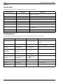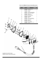
1
GP350
Portable Radios
146-174 MHz
438-470 MHz
6880904Z07-O
*6880904Z07*
*6880904Z07*
6880904Z07-O
Motorola
Radius Division
Hwy 34 West
Mt. Pleasant, IA 52641
Computer Software Copyrights
The Motorola products described in this manual may include copyrighted Motorola computer programs stored in semiconductor memories or other
media. Laws in the United States and other countries preserve for Motorola certain exclusive rights for copyrighted computer programs, including
the exclusive right to copy or reproduce in any form, the copyrighted computer program. Accordingly, any copyrighted Motorola computer programs contained in the Motorola products described in this manual may not be copied or reproduced in any manner without the express written permission of Motorola. Furthermore, the purchase of Motorola products shall not be deemed to grant, either directly or by implication, estoppel or
otherwise, any license under the copyrights, patents or patent applications of Motorola, except for the normal non-exclusive royalty-free license to
use that arises by operation of law in the sale of a product.
Airbag Warning Statement
!
WARNING
VEHICLES EQUIPPED WITH AIR BAGS
An air bag inflates with great force. DO NOT place objects, including communication equipment,
in the area over the air bag or in the air bag deployment area. If the communication equipment is
improperly installed and the air bag inflates, this could cause serious injury.
• Installation of vehicle communication equipment should be performed by a professional
installer/technician qualified in the requirements for such installations. An air bag’s size, shape and
deployment area can vary by vehicle make, model and front compartment configuration (e.g.,
bench seat vs. bucket seats).
• Contact the vehicle manufacturer’s corporate headquarters, if necessary, for specific air bag
information for the vehicle make, model and front compartment configuration involved in your
communication equipment installation.
Table of Contents
Scope of Manual . . . . . . . . . . . . . . . . . . . . . . . . . . . . . . . . . . . . . . . . . . . . . . . . . . . . . . . . . . . . . . v
How to Use This Manual . . . . . . . . . . . . . . . . . . . . . . . . . . . . . . . . . . . . . . . . . . . . . . . . . . . . . . . . v
Other Documentation . . . . . . . . . . . . . . . . . . . . . . . . . . . . . . . . . . . . . . . . . . . . . . . . . . . . . . . . . . . v
Technical Support . . . . . . . . . . . . . . . . . . . . . . . . . . . . . . . . . . . . . . . . . . . . . . . . . . . . . . . . . . . . . v
Service Policy . . . . . . . . . . . . . . . . . . . . . . . . . . . . . . . . . . . . . . . . . . . . . . . . . . . . . . . . . . . . . . . . v
Ordering Replacement Parts . . . . . . . . . . . . . . . . . . . . . . . . . . . . . . . . . . . . . . . . . . . . . . . . . . . . . v
Model Charts . . . . . . . . . . . . . . . . . . . . . . . . . . . . . . . . . . . . . . . . . . . . . . . . . . . . . . . . . . . . . . . . vi
Accessories . . . . . . . . . . . . . . . . . . . . . . . . . . . . . . . . . . . . . . . . . . . . . . . . . . . . . . . . . . . . . . . . . . ix
Performance Specifications . . . . . . . . . . . . . . . . . . . . . . . . . . . . . . . . . . . . . . . . . . . . . . . . . . . . . xi
Service Aids . . . . . . . . . . . . . . . . . . . . . . . . . . . . . . . . . . . . . . . . . . . . . . . . . . . . . . . . . . . . . . . . . xii
Test Equipment . . . . . . . . . . . . . . . . . . . . . . . . . . . . . . . . . . . . . . . . . . . . . . . . . . . . . . . . . . . . . . xii
Test Set Service Cable . . . . . . . . . . . . . . . . . . . . . . . . . . . . . . . . . . . . . . . . . . . . . . . . . . . xiii
Radio Model Information . . . . . . . . . . . . . . . . . . . . . . . . . . . . . . . . . . . . . . . . . . . . . . . . . . . . . xiii
Radio Service Software Information . . . . . . . . . . . . . . . . . . . . . . . . . . . . . . . . . . . . . . . . . . . . . xiv
Configuring the RIB and Radio . . . . . . . . . . . . . . . . . . . . . . . . . . . . . . . . . . . . . . . . . . . . . . . . . xiv
Section 1
Safety Information
General . . . . . . . . . . . . . . . . . . . . . . . . . . . . . . . . . . . . . . . . . . . . . . . . . . . . . . . . . . . . . . . . . . . . 1-1
FCC Safety Information . . . . . . . . . . . . . . . . . . . . . . . . . . . . . . . . . . . . . . . . . . . . . . . . . . . . . . . 1-1
Section 2
Intrinsically Safe Radio Information
FMRC Approved Equipment . . . . . . . . . . . . . . . . . . . . . . . . . . . . . . . . . . . . . . . . . . . . . . . . . . .
Repair of FMRC Approved Products . . . . . . . . . . . . . . . . . . . . . . . . . . . . . . . . . . . . . . . . . . . .
Repair . . . . . . . . . . . . . . . . . . . . . . . . . . . . . . . . . . . . . . . . . . . . . . . . . . . . . . . . . . . . . . . .
Relabeling . . . . . . . . . . . . . . . . . . . . . . . . . . . . . . . . . . . . . . . . . . . . . . . . . . . . . . . . . . . . .
Do Not Substitute Options or Accessories . . . . . . . . . . . . . . . . . . . . . . . . . . . . . . . . . . . .
2-1
2-1
2-2
2-2
2-2
Section 3
Disassembly/Reassembly
Remove Battery . . . . . . . . . . . . . . . . . . . . . . . . . . . . . . . . . . . . . . . . . . . . . . . . . . . . . . . . . . . . .
Remove Belt Clip from Battery . . . . . . . . . . . . . . . . . . . . . . . . . . . . . . . . . . . . . . . . . . . . . . . . .
Remove Chassis . . . . . . . . . . . . . . . . . . . . . . . . . . . . . . . . . . . . . . . . . . . . . . . . . . . . . . . . . . . . .
Remove the Main Board . . . . . . . . . . . . . . . . . . . . . . . . . . . . . . . . . . . . . . . . . . . . . . . . . . . . . .
Re-assembly of Radio . . . . . . . . . . . . . . . . . . . . . . . . . . . . . . . . . . . . . . . . . . . . . . . . . . . . . . . .
6880904Z07-O
3-1
3-1
3-1
3-2
3-2
i
GP350 Portable Radios Service Manual
Section 4
Theory of Operation
Overview . . . . . . . . . . . . . . . . . . . . . . . . . . . . . . . . . . . . . . . . . . . . . . . . . . . . . . . . . . . . . . . . . . 4-1
Microcomputer . . . . . . . . . . . . . . . . . . . . . . . . . . . . . . . . . . . . . . . . . . . . . . . . . . . . . . . . . . . . . . 4-1
Microcomputer Power-Up and Reset Routine . . . . . . . . . . . . . . . . . . . . . . . . . . . . . . . . . 4-1
Receiver . . . . . . . . . . . . . . . . . . . . . . . . . . . . . . . . . . . . . . . . . . . . . . . . . . . . . . . . . . . . . . . . . . . 4-1
Intermediate Frequency (IF) . . . . . . . . . . . . . . . . . . . . . . . . . . . . . . . . . . . . . . . . . . . . . . . 4-2
Transmitter . . . . . . . . . . . . . . . . . . . . . . . . . . . . . . . . . . . . . . . . . . . . . . . . . . . . . . . . . . . . . . . . . 4-2
Frequency Generation Circuitry . . . . . . . . . . . . . . . . . . . . . . . . . . . . . . . . . . . . . . . . . . . . . . . . 4-3
Synthesizer . . . . . . . . . . . . . . . . . . . . . . . . . . . . . . . . . . . . . . . . . . . . . . . . . . . . . . . . . . . . 4-3
VCO . . . . . . . . . . . . . . . . . . . . . . . . . . . . . . . . . . . . . . . . . . . . . . . . . . . . . . . . . . . . . . . . . 4-3
TX Audio Path . . . . . . . . . . . . . . . . . . . . . . . . . . . . . . . . . . . . . . . . . . . . . . . . . . . . . . . . . 4-4
Internal MIC Bias Switch and External PTT Sense Circuits . . . . . . . . . . . . . . . . . . 4-4
MIC Amplifier . . . . . . . . . . . . . . . . . . . . . . . . . . . . . . . . . . . . . . . . . . . . . . . . . . . . . 4-4
TX Audio Mute Gate . . . . . . . . . . . . . . . . . . . . . . . . . . . . . . . . . . . . . . . . . . . . . . . . 4-4
Pre-emphasis Amplifier (standard models) . . . . . . . . . . . . . . . . . . . . . . . . . . . . . . . 4-4
Option Interface Connector P1 (Keypad/Display models) . . . . . . . . . . . . . . . . . . . 4-4
Limiter (Audio Filter IC) . . . . . . . . . . . . . . . . . . . . . . . . . . . . . . . . . . . . . . . . . . . . . 4-5
Post-Limiter Filter (Audio Filter IC) . . . . . . . . . . . . . . . . . . . . . . . . . . . . . . . . . . . . 4-5
PL Encoder . . . . . . . . . . . . . . . . . . . . . . . . . . . . . . . . . . . . . . . . . . . . . . . . . . . . . . . 4-5
DTMF Encoder . . . . . . . . . . . . . . . . . . . . . . . . . . . . . . . . . . . . . . . . . . . . . . . . . . . . 4-5
Deviation Attenuators (Audio Filter IC) . . . . . . . . . . . . . . . . . . . . . . . . . . . . . . . . . 4-5
RX Audio Path . . . . . . . . . . . . . . . . . . . . . . . . . . . . . . . . . . . . . . . . . . . . . . . . . . . . . . . . . 4-5
PL Rejection Filter (Audio Filter IC) . . . . . . . . . . . . . . . . . . . . . . . . . . . . . . . . . . . 4-5
PL Decoder . . . . . . . . . . . . . . . . . . . . . . . . . . . . . . . . . . . . . . . . . . . . . . . . . . . . . . . 4-5
Center-Slicer . . . . . . . . . . . . . . . . . . . . . . . . . . . . . . . . . . . . . . . . . . . . . . . . . . . . . . 4-5
Option Interface Connector P1 (Keypad/Display Models) . . . . . . . . . . . . . . . . . . . 4-5
RX Audio Mute Gate . . . . . . . . . . . . . . . . . . . . . . . . . . . . . . . . . . . . . . . . . . . . . . . . 4-6
Audio Power Amplifier . . . . . . . . . . . . . . . . . . . . . . . . . . . . . . . . . . . . . . . . . . . . . . 4-6
Noise Squelch Attenuator . . . . . . . . . . . . . . . . . . . . . . . . . . . . . . . . . . . . . . . . . . . . 4-6
Vox Circuit Operation . . . . . . . . . . . . . . . . . . . . . . . . . . . . . . . . . . . . . . . . . . . . . . . 4-6
GP350 Portable Radio Functional Block Diagram . . . . . . . . . . . . . . . . . . . . . . . . . . . . . . . . . . 4-7
Receiver, Transmitter, VCO, Synthesizer, and AFIC Block Diagrams . . . . . . . . . . . . . . . . . . . 4-8
Section 5
Troubleshooting
Overview . . . . . . . . . . . . . . . . . . . . . . . . . . . . . . . . . . . . . . . . . . . . . . . . . . . . . . . . . . . . . . . . . . 5-1
Troubleshooting Charts . . . . . . . . . . . . . . . . . . . . . . . . . . . . . . . . . . . . . . . . . . . . . . . . . . . . . . . 5-1
Troubleshooting Flow Chart for Receiver . . . . . . . . . . . . . . . . . . . . . . . . . . . . . . . . . . . . . . . . . 5-2
Troubleshooting Flow Chart for Transmitter . . . . . . . . . . . . . . . . . . . . . . . . . . . . . . . . . . . . . . . 5-3
Troubleshooting Flow Chart for Synthesizer . . . . . . . . . . . . . . . . . . . . . . . . . . . . . . . . . . . . . . . 5-4
Troubleshooting Flow Chart for Microprocessor . . . . . . . . . . . . . . . . . . . . . . . . . . . . . . . . . . . 5-5
Troubleshooting Flow Chart for VCO . . . . . . . . . . . . . . . . . . . . . . . . . . . . . . . . . . . . . . . . . . . . 5-6
ii
6880904Z07-O
August, 1996
GP350 Portable Radios Service Manual
Section 6
Component Location Diagrams, Schematic Diagrams,
Exploded Views, and Parts Lists
General . . . . . . . . . . . . . . . . . . . . . . . . . . . . . . . . . . . . . . . . . . . . . . . . . . . . . . . . . . . . . . . . . . . . 6-1
Controller . . . . . . . . . . . . . . . . . . . . . . . . . . . . . . . . . . . . . . . . . . . . . . . . . . . . . . . . . . . . . . . . . . 6-1
Transceiver . . . . . . . . . . . . . . . . . . . . . . . . . . . . . . . . . . . . . . . . . . . . . . . . . . . . . . . . . . . . . . . . . 6-1
Schematic Notes . . . . . . . . . . . . . . . . . . . . . . . . . . . . . . . . . . . . . . . . . . . . . . . . . . . . . . . . . . . . . 6-1
Parts List: 0180702Y89 Battery Filter Board. . . . . . . . . . . . . . . . . . . . . . . . . . . . . . . . . . . . . . . 6-1
Parts List: Flex Circuit . . . . . . . . . . . . . . . . . . . . . . . . . . . . . . . . . . . . . . . . . . . . . . . . . . . . . . . . 6-1
Component Location Diagrams, Schematic Diagrams, and Parts Lists for
Battery Filter Board and Flex Circuit . . . . . . . . . . . . . . . . . . . . . . . . . . . . . . . . . . . . . . . . . . 6-1
Component Location Diagram for HLD9440A and HLD9441A
VHF, 146-174MHz, Transceiver and Controller . . . . . . . . . . . . . . . . . . . . . . . . . . . . . . . . . 6-2
Schematic Diagram for HLD9440A and HLD9441A
VHF, 146-174MHz, Transceiver Section . . . . . . . . . . . . . . . . . . . . . . . . . . . . . . . . . . . . . . 6-3
Component Location Diagram for HLE9480A and HLE9481A
UHF, 438-470MHz, Transceiver Section . . . . . . . . . . . . . . . . . . . . . . . . . . . . . . . . . . . . . . . 6-4
Schematic Diagram for HLE9480A and HLE9481A
UHF, 438-470MHz, Transceiver Section . . . . . . . . . . . . . . . . . . . . . . . . . . . . . . . . . . . . . . . 6-5
Schematic Diagram for Controller Section . . . . . . . . . . . . . . . . . . . . . . . . . . . . . . . . . . . . . . . . 6-6
Parts List: Controller Components (for all bandsplits) . . . . . . . . . . . . . . . . . . . . . . . . . . . . . . . 6-7
Parts List: HLD9440A and HLD9441A, 146-174MHz VHF Transceiver. . . . . . . . . . . . . . . . . 6-8
Parts List: HLE9480A and HLE9481A, 438-470MHz UHF Transceiver . . . . . . . . . . . . . . . . . 6-9
Parts List: GP350 Basic Mechanical . . . . . . . . . . . . . . . . . . . . . . . . . . . . . . . . . . . . . . . . . . . . 6-10
HLN9960A DTMF Circuit Board Detail . . . . . . . . . . . . . . . . . . . . . . . . . . . . . . . . . . . . . . . . . 6-11
HLN9960A DTMF Schematic Diagram and Parts List . . . . . . . . . . . . . . . . . . . . . . . . . . . . . . 6-12
Battery Chargers Single and Multi-Unit Rapid Rate (1 Hour) . . . . . . . . . . . . . . . . . . . . . . . . . 6-13
Battery Chargers Single and Multi-Unit Rapid Rate (1 Hour) . . . . . . . . . . . . . . . . . . . . . . . . . 6-14
Battery Chargers Standard Rate (10 Hour) . . . . . . . . . . . . . . . . . . . . . . . . . . . . . . . . . . . . . . . 6-15
Battery Chargers Standard Rate (10 Hour) . . . . . . . . . . . . . . . . . . . . . . . . . . . . . . . . . . . . . . . 6-16
Schematic Diagram and Parts List for HMN9041A Remote Speaker/Microphone . . . . . . . . 6-17
Exploded View and Parts List for HMN9041A Remote Speaker/Microphone . . . . . . . . . . . . 6-18
August, 1996
6880904Z07-O
iii
GP350 Portable Radios Service Manual
iv
6880904Z07-O
August, 1996
GP350 Portable Radios Service Manual
Foreword
Scope of Manual
Scope of Manual
This manual is intended for use by experienced technicians
familiar with similar types of equipment. It contains all service information required for the equipment described and is
current as of the printing date. Changes which occur after the
printing date are incorporated by instruction manual revision. These revisions are added to the manuals as the engineering changes are incorporated into the equipment.
How to Use This Manual
This manual contains introductory material such as model
charts, accessories, and specifications, as well as four sections that deal with specific service aspects of the GP350.
Refer to the Table of Contents for a general overview of the
manual, or to the “Overview” paragraph in each section for
a specific overview of the information in that section.
Other Documentation
Table 1 lists other documentation for the GP350 Portable
Radios.
Table 1.
Other Documentations
Information
Basic Use of GP350
Programming
chassis or kit which contains the part, and a detailed description of the desired component. If a Motorola part number is
identified on a parts list, you should be able to order the part
through Motorola Parts. If only a generic part is listed, the
part is not normally available through Motorola. If no parts
list is shown, generally, no user serviceable parts are available for the kit.
Technical Support (U.S. and Canada)
Radius Product Services
Hwy. 34 West
Mt. Pleasant, IA 52641 USA
1-800-356-1520 (U.S. and Canada)
319-385-5395 (Outside U.S.)
Technical Support (Latin America, Mexico, Caribbean)
1-800-694-2161 (Latin America, Mexico, Caribbean)
Radius 30-Day Warranty
Radius Repair Depot
Attention: Warranty Return
1000 W. Washington Street
Mt. Pleasant, IA 52641 USA
1-800-356-1520
319-385-5395 (Outside U.S.)
Radius Major Component Repair
Radius Repair Depot
1000 W. Washington Street
Mt. Pleasant, IA 52641 USA
Location
GP350 User Guide (6880904Z01)
GP350 RSS Manual (6880904Z09)
Technical Support
To obtain technical support, you may call Motorola’s Radius
Product Services. When you call, we ask that you have ready
the model and serial numbers of the respective radio or its
parts.
Service Policy
If malfunctions occur within 30 days that cannot be resolved
over the phone with Radius Product Services, a defective
major component should be returned. You must obtain authorization from Radius Product Services before returning the
component.
Motorola Parts
Americas Parts Division
Attention: Order Processing
1313 E. Algonquin Road
Schaumburg, IL 60196
Customer Service Motorola Parts
1-800-422-4210
1-708-538-8198 (FAX)
Parts Identification
1-708-538-0021
1-708-538-8194 (FAX)
Ordering Replacement Parts
You can order additional components and some piece parts
directly through your Radius price pages. When ordering
replacement parts, include the complete identification number for all chassis, kits, and components. If you do not know
a part number, include with your order the number of the
August, 1996
6880904Z07-O
v
Foreword
GP350 Portable Radios Service Manual
Model Charts
Description
2-Chan., 20/25 kHz (146-174 MHz)
16-Chan., 20/25 kHz (146-174 MHz)
Model
P93MGC20A2A_
P93MGC20C2A_
Model Charts
GP350
VHF
146 - 174 MHz
X = Indicates one of each required
Item
X
X
X
HHN9126_
Housing
HLD9440_
RF Board, 2-Chan., 20/25 kHz, (146-174 MHz)
X
HLD9441_
RF Board, 16-Chan., 20/25 kHz, (146-174 MHz)
X
X
HLN8255_
Spring-Action Belt Clip, 3”
X
X
HLN9152_
Chassis Hardware Assembly
HLN9202_
2-Channel Control Kit
X
vi
Description
X
HLN9203_
16-Channel Control Kit
X
X
NAD6502_
Antenna (146-174 MHz)
X
X
6880904Z01
Users Guide/Quick Reference Card
6880904Z07-O
August, 1996
GP350 Portable Radios Service Manual
Foreword
Description
2-Chan., 20/25 kHz (438-470 MHz)
16-Chan., 20/25 kHz (438-470 MHz)
Model
P94MGC20A2A_
P94MGC20C2A_
Model Charts
GP350
UHF
438 - 470 MHz
X = Indicates one of each required
Item
X
X
Description
HHN9126_
Housing
HLE9480_
RF Board, 2-Chan., 20/25 kHz (438-470 MHz)
X
HLE9481_
RF Board, 16-Chan., 20/25KHz, (438-470 MHz)
X
X
HLN8255_
Spring-Action Belt Clip, 3”
X
X
HLN9152_
Chassis Hardware Assembly
HLN9202_
2-Channel Control Kit
X
HLN9203_
16-Channel Control Kit
X
X
NAE6483_
Antenna
X
X
6880904Z01
User Guide /Quick Reference Card
X
X
August, 1996
6880904Z07-O
vii
Foreword
GP350 Portable Radios Service Manual
16-Chan., 12.5 kHz (490-520 MHz)
P94MGC00C4A_
16-Chan., 20/25 kHz (490-520 MHz)
P94MGC20C4A_
16-Chan., 12.5 kHz (465-495 MHz)
P94MGC00C3A_
16-Chan., 20/25 kHz (465-495 MHz)
P94MGCC20C3A_
Model
Description
Model Charts
GP350
UHF
465 - 495 MHz
490 - 520 MHz
X = Indicates one of each required
This page has been intentionally left blank.
Item
X
X
X
X
viii
Description
HLE9487_
RF Board, 12.5 kHz, (465-495 MHz)
HLE9485_
RF Board, 20/25 kHz, (465-495 MHz)
HLE9488_
RF Board, 12.5 kHz, (490-520 MHz)
HLE9489_
RF Board, 20/25 kHz, (490-520 MHz)
X
X
X
X
HLN9203_
16-Channel Control Kit
X
X
X
X
HLN9152_
Chassis Hardware Assembly
X
X
X
X
HHN9126_
Housing
X
X
X
X
NAE6483_
Antenna
X
X
X
X
6880904z01
User Guide/Quick Reference Card
6880904Z07-O
August, 1996
GP350 Portable Radios Service Manual
Foreword
Accessories
Accessories
Antennas:
NAD6502_R — Black
146-174 MHz VHF Antenna (Standard w/Unit)
HAD9742
— Black
146-162 MHz VHF Stubby Antenna
HAD9743
— Blue
162-174 MHz VHF Stubby Antenna
NAE6483_R — None
403-520 MHz UHF Antenna (Standard w/Unit)
NAE6521_R — Red
400-440 MHz UHF Stubby Antenna
NAE6522_R — Green
438-470 MHz UHF Stubby Antenna
HAD9728
Tunable Antenna Kit (136-174 MHz)
— None
Note:
Each of the color coded antennas listed is designed to cover only the frequency split indicated. Therefore, it is
important to order the correct antenna (frequency split) to match a specific customer frequency.
Carrying Accessories:
HLN9417
Standard Leather Carry Case w/Belt Loop
HLN9323
Standard Leather Carry Case w/Swivel
HLN9416
Standard Nylon Carry Case
HLN9420
DTMF Standard Leather Carry Case w/Belt Loop
HLN9418
DTMF Standard Leather Carry Case w/Swivel
HLN9724
2-1/2” Belt Clip
HLN8255
Replacement Heavy Duty Spring Action 3” Belt Clip
HLN8052
Wrist Strap
NTN5243
Shoulder Strap (for all carry cases)
HLN8414
Chest Pack Carry Holder
42-5857B04
Replacement 3” Swivel Belt Loop (for use with same carry accessories as 2-1/2” Belt
Loop but with wider belts)
42-5857B05
Replacement 2-1/2” Swivel Belt Loop (for use with HLN9323, HLN9418)
42-80532B01
Replacement Strap for Nylon and Leather Carry Cases
42-80532B02
Replacement Strap for DTMF Carry Case
HLN9985
Waterproof Bag
August, 1996
6880904Z07-O
ix
Foreword
GP350 Portable Radios Service Manual
Accessories
Nickel-Cadmium Battery Chargers:
HTN9630
HTN9702
HTN9748
HTN9802
HTN9804
HTN9811
HTN9803
HTN9805
HTN9812
HLN9719
HLN9944
120 Volt - 1 Hour Rapid Rate Charger
120 Volt - 10 Hour Standard Rate Charger
120 Volt - 6 Unit - 1 Hour Rapid Rate Charger
220 Volt - 1 Hour Rapid Rate Charger (European Plug)
220 Volt - 10 Hour Standard Rate Charger (European Plug)
220 Volt - 6 Unit - 1 Hour Rapid Rate Charger (European Plug)
240 Volt - 1 Hour Rapid Rate Charger (U. K. Plug)
240 Volt - 10 Hour Standard Rate Charger (U. K. Plug)
240 Volt - 6 Unit - 1 Hour Rapid Rate Charger (U. K. Plug)
1 Hour Vehicular Charger Adapter/Bracket (12 volt for use with HTN9630 Rapid Rate Charger)
Wall Mounting Bracket For Multi Unit Charger
Batteries:
HNN9360
HNN9361
1200 mAH High Capacity Battery (Standard)
1200 mAH (Fully Approved FM Battery)
Audio/RF Accessories:
HMN9041
BDN6720*
HMN9752_R*
50-80386B90
50-80371E73
HMN9754_R*
HMN9013*
BDN6647*
HMN9021*
HMN9022*
BDN6648*
BDN6646*
BDN6706*
HLN9756
HLN9482
Remote Speaker Microphone (with GP350 connector)
Earpiece Without Volume Control (plastic earloop)
Earpiece With Volume Control (plastic earloop)
Rubber Ear Inserts for Earpieces (with older metal earloop - pkg q. 25)
Rubber Ear Inserts for Earpieces (with plastic earloop - pkg q. 25)
2 Piece Surveillance Microphone (plastic earloop)
Light Weight Headset II
Medium Weight Single Speaker Headset w/Swivel Boom Microphone (compatible with
Internal VOX)
Medium Weight Dual Muff Headset w/Swivel Boom Microphone (Over the Head)
Medium Weight Dual Muff Headset w/Swivel Boom Microphone (Behind the Head)
Heavy Weight Headset w/Noise Cancelling Boom Microphone with PTT button (compatible with
Internal VOX)
Ear Microphone with PTT Interface
Ear Microphone w/VOX Interface (External VOX Included)
BNC - RF Adapter (for use with P110, GP300 and GP350 models only)
GP300 to GP350 Accessory Adapter
Prices And Availability Subject To Change Without Notice
* Accessories marked with an asterisk (*) require the HLN9482 (GP300 to GP350 Adapter Kit) for use on GP350 radios.
x
6880904Z07-O
August, 1996
GP350 Portable Radios Service Manual
Foreword
Performance Specifications
Performance Specifications
GENERAL
Model Series:
VHF
UHF
P93MGC
P94MGC
Frequency:
146-174
Channel Capacity:
438-470
2 or 16 channels
2 or 16 channels
Power Supply:
One (1) rechargeable Nickel-Cadmium battery (7.5V)
Dimensions†:
5.54” X 2.48” X 1.79” (142 X 63X 45.6mm)†
Weight †:
17.8 oz. (509 g)†
Average Battery Life
(5-5-90 Duty Cycle):
High Capacity:
Low Power
10.5 Hours
Environmental:
High Power
8 Hours
Low Power
10.5 Hours
High Power
8 Hours
Meets MIL-STD-810-C, D, and E & EIA RS-316B environmental specifications for vibration, shock, rain, dust, and
humidity
†Standard High Capacity Battery Model
RECEIVER
TRANSMITTER
VHF
RF Output @ 7.5V:
Freq. Separation:
Freq. Stability
(-30˚C to +60˚):
Modulation:
High
5W
Low
1W
High
4W†
26, 28 MHz
±0.0005%
±5 kHz max. (25/30 kHz channel spacing)
±2.5 kHz max. (12.5 kHz channel spacing)
0.25 µW < 2GHz
Audio Response:
(from 6 dB/oct.
Pre-Emphasis,
300 to 3000Hz
+1, -3 dB
Audio Distortion: @
1000 Hz, 60% Rated
Max. Dev.
FM Noise:
Low
1W
30, 32 MHz
Spurs/Harmonics:
FCC
Designation:
VHF
UHF
Freq Separation:
Sensitivity
- 20 dB Quieting†:
12 dB EIA SINAD†:
20 dB SINAD†:
25 kHz
12.5 kHz
AZ489FT4802
AZ489FT4803
AZ489FT4804
AZ489FT4805
-40 dB‡
†Max.RF output is 3W for frequencies greater than 512 MHz
‡Typical level
25 kHz
26, 28 MHz
0.32 µV
0.22 µV
0.30 µV
Squelch
Sensitivity:
12.5 kHz
30, 32 MHz
0.38 µV
N/A
0.35 µV
0.32 µV
0.22 µV‡
0.30 µV
0.38 µV
N/A
0.35 µV
10 dB SINAD
Selectivity:
70dB
60dB
70dB
60dB
Intermodulation
70dB
60 dB
70 dB
60 dB
Freq. Stability
(-30˚C to +60˚C):
(-10˚C to +50˚C):
<3%
AZ489FT3784
AZ489FT3785
Channel Spacing:
UHF
0.0005%
0.0003%
Spur Rejection
EIA:
CEPT:
Image Rejection
EIA:
CEPT:
Audio Output
at<10% Distortion
(1 kHz)
75 dB
70 dB
75 dB
70 dB
70 dB
70 dB
500mW
†Typical specification is 0.28mV on frequencies greater than 512 MHz
*All specifications subject to change without notice.
August, 1996
6880904Z07-O
xi
Foreword
GP350 Portable Radios Service Manual
Service Aids
Service Aids
The following table lists service aids recommended for working on the GP350.
Motorola Part No.
Description
Application
HLN9214
Radio Interface Box
Enables communication between the radio and the computer’s serial
communications adapter.
HSN9412
RIB Power Supply
Used to supply power to the RIB.
HKN9216
Computer Interface Cable
Connects the computer’s serial communications adapter to the RIB.
HLN9390
AT to XT Computer Adapter
Allows HKN9216 to plug into a XT style communications port.
HKN9857
Programming / Test Cable
Connects radio to RIB. And can be used as a Battery Eliminator.
HVN9128
Radio Service Software
Software on 3-1/2 in. diskette
HLN9482
GP300 to GP350 Accessory
Adapter
Allows use of the RKN4034 Test Set Cable with the GP350 radio.
RTX4005
Portable Test Set
Enables connection to the audio / accessory jack. Allows switching
for radio testing.
RKN4034
Test Set Cable
Connects radio to RTX4005B Test Box.
REX1143
Programming Adapter Kit
Connects radio to programmer (HKN9857)
Test Equipment
The following table lists test equipment required to service the GP350 and other two-way radios.
Motorola Model No.
Description
Characteristics
R2200, R2400, or R2001D
with trunking option
Service Monitor
*R1049A
Digital Multimeter
*S1100A
Audio Oscillator
67 to 161.4Hz tones
Used with service monitor for injection of PL
tones
*S1053D,
*SKN6009A,
*SKN6001A
AC Voltmeter, Power Cable for meter, Test leads
for meter
1mV to 300V, 10-Megohm
input impedance
Audio voltage measurements
R1053
Dual-trace Oscilloscope
20 Mhz bandwidth,
5mV/cm - 20V/cm
Waveform measurements
*S1350C, *ST1215B
(VHF) *ST1223B (UHF)
*T1013A
Wattmeter, Plug-in Elements (VHF& UHF), RF
Dummy Load
50-ohm, + 5% accuracy 10
Watts, maximum 0-1000
Mhz, 300W
Transmitter power output measurements
S1339A
RF Millivolt Meter
100uV to 3V rf, 10 khz to 1.2
Ghz
RF level measurements
*R1013A
SINAD Meter
S1347D or
S1348D (prog)
DC Power Supply
xii
This monitor will substitute
for items with an asterisk *
Application
Frequency/deviation meter and signal generator for wide-range troubleshooting and
alignment
Two meters recommended for ac/dc voltage
and current measurements
Receiver sensitivity
0-20 Vdc, 0-5 Amps
6880904Z07-O
Bench supply for 10Vdc
August, 1996
GP350 Portable Radios Service Manual
Foreword
Radio Model Information
Test Set Service Cable
P1
NOTE: Pins 2 and 7
are cut.
4
tip
6
12
6
12
14 Speaker (Hi)
3.5 mm plug
5
Ground
47 ohm, 1/2w
sleeve
7
3
2
External
Select
External
Speaker
14
8
11
1
9
+ 1.0 uF
sleeve
Speaker
Common
External
Microphone
tip
2.5 mm plug
(P1) DETAIL
FRONT SIDE
33k, 1/8 w
VIEWED FROM POGO PIN
SIDE OF ADAPTER
9 Speaker (Lo)
11
2
3 Gnd
4 Mic. Audio
5 PTT
1
7
8
MAEPF-25490-O
NOTE: For proper speaker impedance, the RTX4005B
test set Audio out switch must be set to the “MX” position
Figure 1.
Service Cable (RKN4034A) for the Test Set (RTX4005B)
Radio Model Information
The model number, serial number, and Motorola FCC designation number are all on a label attached to the back of your radio. From
this model number, you can determine the RF output power, frequency band, type of squelch, and number of channels. The table
below outlines one portable radio model number and its specific characteristics.
All GP350 radio models are synthesized, two or sixteen channel units that come standard with tone Private-Line (TPL) or Digital Private-Line (DPL) coded squelch, which may be enabled / disabled on a per channel basis. Programming changes can be
made by your local Motorola Radius dealer.
Radio Model Number (Example: P94MGC20C2AA)
Type
of
Unit
Tx Power
P
Freq.
Model
Series
Channel
Spacing
Channel
Capability
Frequency
Sub-band
Version
9
3
MGC
00
A
1
A
1-5 W VHF
1-4 W UHF
VHF
Universal
12.5 kHz
2 Channels
Low Split
4
20
2, 3 or 4
UHF
20/25 kHz
High Split
P = Portable
C
16 Channels
August, 1996
6880904Z07-O
Unique
Model
Variation
A
A = Package Model with
Battery, Antenna, Belt Clip,
Charger.
xiii
Foreword
GP350 Portable Radios Service Manual
Radio Service Software Information
Radio Service Software Information
To run the Radio Service Software, you will need the following equipment:
Required Equipment:
1. IBM XT, AT, Convertible, or System/2 Model 30/50TM with 512K RAM, Dual Floppy Disk Drives or on Floppy Disk
and one Hard Disk.
2. PCDOSTM or MSDOSTM 3.0 or later.
3. Radio Interface Box (RIB) HLN9214.
4. RIB to IBM AT cable HKN9216.
5. IBM AT cable to IBM XT computer adapter (optional) HLN9390.
6. Programming/Test cable (HKN9857).
7. Programming Hardware Kit (REX1143).
8. RIB power supply HSN9412 (110 VAC) or 0180358A56 (220 VAC).
9. Power Supply R1011A or equivalent.
RSS Manual
HVN9128
Software
Computer
Power Supply (7.2 VDC)
Note: Battery can be used on
programming cable making
power supply optional.
HLN9214
(RIB)
HKN9857
Programming / test cable.
Plugs between the RIB and radio.
HKN9216
RIB to Computer Cable
Plugs into RIB and
computer.
HSN9412
RIB Power Supply.
Plug into 110 VAC
outlet
GP350 Radio
Figure 2.
Equipment Setup
Configuring the RIB and Radio
xiv
1.
Connect the RIB to the computer (Figure 2).
2.
If your computer has an XT style communications port (25 pin connector), plug the HLN9390 adapter into the computer and plug the HKN9216 cable into the adapter. If you are unsure of which connection is on the back of your
computer or the COM port, then please consult the computer manuals.
3.
Plug the large 25 pin end of the HKN programming cable into the RIB. The other end of this cable has a “battery
eliminator.”
4.
Connect the two adapter plates (REX1143) to HKN9857 according to the instructions supplied with the Programming
Hardware Kit.
5.
Slide the battery eliminator in place of the radio’s battery.
6.
Plug the HSN9412 power supply into a wall outlet, and connect the other end to the RIB.
7.
Connect the radio to a power supply and turn the volume control clockwise to turn it on.
6880904Z07-O
August, 1996
Section 1
Safety Information
General
FCC Safety Information
This manual includes specifications, fundamental disassembly/reassembly procedures, schematic diagrams, component
location diagrams, flex circuit diagrams, several parts lists,
theory of operation, and troubleshooting sections to cover
the GP350 radios. Hereafter, the text will refer collectively to
the GP350 radios as “this family of radios.” For operation of
the radio, refer to the applicable manual available separately.
Throughout the text in this publication, you will notice the
use of warnings, cautions, and notes. These notations are
used to emphasize that safety hazards exist, and care must be
taken and observed.
The Federal Communications Commission (FCC), with its
action in General Docket 79-144, March 13, 1985, has
adopted a safety standard for human exposure to radio frequency (RF) electromagnetic energy emitted by FCC-regulated equipment. Motorola subscribes to the same safety
standards for the use of its products. Proper operation of this
radio will result in user exposure substantially below the
FCC recommended limits.
!
WARNING
An operational procedure, practice, or condition, etc., which may result in injury or death
if not carefully observed.
!
Do not hold the radio with the antenna very close to, or
touching, exposed parts of the body, especially the face,
ears, or eyes, while transmitting. Hold the radio in a vertical position with the microphone two to three inches
away from the lips.
•
Do not hold the transmit switch (PTT) on when not actually desiring to transmit.
•
Do not allow children to play with any radio equipment
containing a transmitter.
•
Do not operate this equipment near electrical blasting
caps or in an explosive atmosphere. Under certain conditions, radios can interfere with blasting operations.
When you are in the vicinity of construction work, look
for, and observe, signs cautioning against radio transmission. If radio transmission is prohibited, you must
not transmit until out of the area. Furthermore, you must
turn off your radio to prevent any accidental transmission.
•
Do not replace or charge batteries in a hazardous atmosphere. Contact sparking may occur while installing or
removing batteries and cause an explosion.
•
Turn radio off when removing or installing a battery.
CAUTION
An operational procedure, practice, or condition, etc., which may result in damage to the
equipment if not carefully observed.
NOTE
An operational procedure, practice, or condition, etc., which is essential to emphasize.
August, 1996
•
6880904Z07-O
1-1
Safety Information
GP350 Portable Radios Service Manual
FCC Safety Information
This page has been intentionally left blank.
1-2
6880904Z07-O
August, 1996
Section 2
Intrinsically Safe Radio Information
FMRC Approved Equipment
Anyone intending to use a radio in a location where hazardous concentrations of flammable material exist (hazardous
atmosphere) is advised to become familiar with the subject
of intrinsic safety and with the National Electric Code NFPA
70 (National Fire Protection Association) Article 500 (hazardous [classified] locations).
An Approval Guide, issued by Factory Mutual Research
Corporation (FMRC), lists manufacturers and the products
approved by FMRC for use in such locations. FMRC has
also issued a voluntary approval standard for repair service
(“Class Number 3605”)
Do not disassemble the FMRC Approved
Product unit in any way that exposes the
internal electrical circuits of the unit.
Radios must ship from the Motorola manufacturing facility
with the hazardous atmosphere capability and FM Approval
labeling. Radios will not be “upgraded” to this capability and
labeled in the field.
A modification changes the unit’s hardware from its original
design configuration. Modifications can only be done by the
original product manufacturer at one of its FMRC audited
manufacturing facilities.
FMRC Approval labels are attached to the radio to identify
the unit as being FM Approved for specified hazardous atmospheres. This label specifies the hazardous Class/Division/
Group along with the part number of the battery that must be
used. Their Approval mark is shown below.
!
FM
APPROVED
!
WARNING
Do not operate radio communications equipment in a hazardous atmosphere unless it is a
type especially qualified (e.g. FMRC
Approved) for such use. An explosion or fire
may result.
Do not operate the FMRC Approved Product
in a hazardous atmosphere if it has been physically damaged (e.g. cracked housing). An
explosion or fire may result.
Repair of FMRC Approved Products
REPAIRS FOR MOTOROLA FMRC APPROVED
PRODUCTS ARE THE RESPONSIBILITY OF THE
USER.
You may want to consider using a repair facility that operates
under 3605 repair service approval.
Do not replace or charge batteries in a hazardous atmosphere. Contact sparking may occur
while installing or removing batteries and
cause an explosion or fire.
!
Turn radio off before removing or installing a
battery or accessory.
August, 1996
WARNING
Incorrect repair or relabeling of any FMRC
Approved Product unit could adversely affect
the Approval rating of the unit.
Use of a radio that is not intrinsically safe in
a hazardous atmosphere could result in serious injury or death.
Do not replace or change accessories in a hazardous atmosphere. Contact sparking may
occur while installing or removing accessories and cause an explosion or fire.
Do not operate the FMRC Approved Product
unit in a hazardous location with the accessory contacts exposed. Keep the connector
cover in place when accessories are not used.
WARNING
Failure to use an FMRC Approved Product
unit with an FMRC Approved battery or
FMRC Approved accessories specifically
approved for that product may result in the
dangerously unsafe condition of an unapproved radio combination being used in a
hazardous location.
Unauthorized or incorrect modification of an
FMRC Approved Product unit will negate the
Approval rating of the product.
FMRC’s Approval Standard Class Number 3605 is subject to
change at any time without notice to you, so you may want
to obtain a current copy of 3605 from FMRC. Per the
December, 1994 publication of 3605, some key definitions
and service requirements are as follows:
6880904Z07-O
2-1
Intrinsically Safe Radio Information
GP350 Portable Radios Service Manual
Repair of FMRC Approved Products
Repair
A repair constitutes something done internally to the unit
that would bring it back to its original condition Approved by
FMRC. A repair should be done in an FMRC Approved facility.
Items not considered as repairs are those in which an action
is performed on a unit which does not require the outer casing of the unit to be opened in a manner which exposes the
internal electrical circuits of the unit. You do not have to be
an FMRC Approved Repair Facility to perform these actions.
Relabeling
The repair facility shall have a method by which the replacement of FMRC Approval labels are controlled to ensure that
any relabeling is limited to units that were originally shipped
from the Manufacturer with an FM Approval label in place.
FMRC Approval labels shall not be stocked by the repair
facility. An FMRC Approval label shall be ordered from the
original manufacturer as needed to repair a specific unit.
Replacement labels may be obtained and applied by the
repair facility providing satisfactory evidence that the unit
being relabeled was originally an FMRC Approved unit. Verification may include, but is not limited to: a unit with a damaged Approval label, a unit with a defective housing
displaying an Approval label, or a customer invoice indicating the serial number of the unit and purchase of an FMRC
Approved model.
Do Not Substitute Options or Accessories
The communications equipment package that Motorola submits to FMRC for testing and approval is tested as a system
that consists of the communications unit itself and the battery, antenna and other options or accessories that make up
the rest of the package to be approved. This approved package must be strictly observed and there must be no substitution of items, even if the substitute you wanted to consider
appears as an approved accessory elsewhere in the Guide for
some other communications equipment unit. Approved configurations are listed by FMRC Approved Product in the
annual Approval Guide published by FMRC. That guide, and
the Approval Standard Class Number 3605 document, can be
ordered from the following address.
Training Resource Center
Publications-Order Processing Dept.
Factory Mutual Engineering and Research
1151 Boston-Providence Turnpike
PO Box 9102
Norwood, MA, 02062
telephone (617) 762-4300
2-2
6880904Z07-O
August, 1996
Section 3
Disassembly/Reassembly
Remove Battery
1.
Locate the battery latch on the bottom of the radio.
Push the battery latch toward the front of the radio
and hold it in the open position as shown in Figure
3-1.
Figure 3-1.MAEPF-25233-O
2.
While holding the battery latch in the open position, slide the battery down approximately 1/2 inch
and then off the radio housing as shown in Figure
3-2.
Figure 3-3.
3.
MAEPF-25235-O
Using a flat-blade screwdriver, carefully pry chassis up on both sides of slot at bottom center of
radio (Figure 3-4).
Chassis to Front Cover
Snaps are Located Here
Figure 3-2.
MAEPF-25234-O
Remove Belt Clip from Battery
Figure 3-4.
MAEPF 25236 O
1.
Push in on tab of belt clip with small flat-bladed
screwdriver, and at the same time slide belt clip
toward top of radio (Figure 3-3).
CAUTION
Lift the chassis approximately half way out
of the front cover, because you must disconnect the flex cable before completely removing the chassis.
Remove Chassis
1.
Pull both control knobs straight off to remove.
2.
Unscrew antenna counterclockwise to remove.
August, 1996
4.
6880904Z07-O
Disconnect the flex cable connector using a flat
blade screwdriver, as shown in Figure 3-5.
3-1
Disassembly/Reassembly
GP350 Portable Radio Service Manual
Remove the Main Board
3.
After all four chassis clips have been removed,
separate the main board from the chassis as shown
in the exploded view Figure 3-7.
Flex Cable
Figure 3-5.
5.
MAEPF-25237-O
Pull the chassis out and away from the housing as
shown by the arrow in Figure 3-5.
Remove the Main Board
1.
2.
The main board is sandwiched between the front
shield and the chassis. Four chassis clips hold the
sandwiched assembly together. Remove the chassis
gasket and place the radio shield side down on a
flat surface.
Using a small flat blade screwdriver, unlock the
four chassis clips while pressing down on the chassis directly above each clip. (Refer to Figure 3-6.)
Figure 1-7.
Figure 3-7.
MAEPF-25239-O
Re-assembly of Radio
Reverse the disassembly procedure.
IMPORTANT
Be sure to reinstall the chassis gasket. This
gasket helps keep the main board free of
unwanted dirt, dust, and water.
Chassis Clips
Figure 3-6.
3-2
6880904Z07-O
August, 1996
Section 4
Theory of Operation
Overview
Receiver
This section provides a detailed theory of operation for the
GP350 and its components: the microcomputer, the receiver,
the transmitter, and the frequency generation circuitry.
The receiver of the GP350 UHF and VHF radios consists of
4 major blocks each: the front-end module, the double balanced mixer, the 45.1 MHz IF and the back-end IF IC.
Microcomputer
The UHF and VHF front-end modules consist of three blocks
of circuitry each: A pre-selector, RF amplifier and a postselector filter. These three items are located on a receiver
module pc-board that stands perpendicular to the main radio
pc-board. This module is enclosed in a shield to prevent radiation into and out of the module. All filters on the UHF and
VHF modules are fixed tuned designs to eliminate the need
for factory tuning and to provide wide-band operation.
The GP350 VHF and UHF radios use the Motorola
68HC11A8 microcomputer, U401, which utilizes:
• 7.9488 MHz clock rate
• Multiplexed 8-bit address/data lines
• 16-bit addressing
The shunt and series coupled resonator topology yields a
more symmetrical frequency response to guard against
strong out of band signals that could produce IM products.
• Internal watchdog circuitry
• Analog to digital conversion input ports
The microcomputer’s operating program is permanently
written or “masked” within the microcomputer. Included in
U401 is an EEPROM memory which stores channel, signalling, and scan list information.
Microcomputer Power-Up and Reset Routine
On power-up U401’s reset line (pin 43) is held low by the
AFIC (U402) until the synthesizer (U201) provides a stable
2.1 MHz output. When U402 releases its control, U401’s
hardware holds the reset line low until it verifies that clock
Y401 is operational. When the reset line goes “high,” U401’s
hardware delays briefly to allow Y401 to stabilize, then the
software begins executing port assignments, RAM checking,
and initialization. A fixed delay of 100 ms is added to allow
the audio circuitry to settle. Next, an alert beep is generated
and the steady state software begins to execute (buttons are
read, radio circuits are controlled).
U401’s reset line can be controlled directly by the 5V regulator (U411), the AFIC, and the microcomputer, and indirectly by the synthesizer. U411 drives the reset line low (via
pin 3) if it loses regulation. This prevents possible latch-up
or overwriting of registers in the microcomputer because the
reset line is higher in voltage than pin 55 of U401 (VDD).
U401 can drive the reset line low if it detects a fault condition
such as an expired watchdog timer, software stuck in an infinite loop, unplanned hardware inputs, static zaps, etc.
The AFIC and synthesizer can control the reset line during
power-up, as outlined above.
August, 1996
The worst case image frequency in the VHF band is
90.2 MHz above the filter passband. The 3 db bandwidth is
approximately 35 MHz, centered at 160 MHz. The center of
the band insertion loss is approximately 1.9 db. The 4-pole
filter is designed to operate with a 50 ohm input termination,
while the output termination is the input impedance of the
RF amplifier that follows it.
The UHF pre-selector filter is a 3-pole,.01 db Chebyshev
bandpass design implemented in a shunt coupled resonator
topology. This topology maximizes the attenuation at the
worst case image frequency for this receiver, which is 90.2
MHz below the filter passband. The 3 db bandwidth is
approximately 45 MHz, centered at 454 MHz. The center of
the band insertion loss is approximately 2.2 db. The 3-pole
filter is designed to operate with a 50 ohm input termination,
while the output termination is the input impedance of the
RF amplifier that follows it.
The RF amplifier, Q1, is a Motorola MMBR571 NPN device
biased in a common emitter configuration. The amplifier is
stabilized by the shunt feedback resistor R3, and has approximately 16.5 db of gain with a noise figure of about 3.0 db
(VHF) and 2.2 db (UHF). The amplifier draws 4 ma of current and is supplied by the receiver 5 volt supply (indicated
as “+5R” on the schematics and block diagrams).
Terminating the RF amplifier is the post-selector filter. This
filter is a 3-pole for VHF and a 4-pole for UHF,.01 db Chebyshev design which is also implemented in a series coupled
resonator topology for maximum image attenuation. The 3
db bandwidth is approximately 38 MHz centered at 160
MHz for VHF and 42.5 MHz centered at 454 MHz for UHF.
6880904Z07-O
4-1
Theory of Operation
GP350 Portable Radios Service Manual
Transmitter
The insertion loss of this filter is approximately 1.9 db for
VHF and 3.5 db for UHF. The filter is designed to be terminated with the amplifier output impedance on one side, and
50 ohm on the other.
The net gain from the receiver module is about (12.2 db
VHF) (10.8 db UHF) in the center of the band and about
(10.7 db VHF) (9.5 db UHF) at the band edges. The net center of the band noise figure is approximately (5.5 db VHF)
(5.2 db UHF). This is sufficient to achieve a typical center of
the band sensitivity of 12 dbs.
The double balanced mixer is composed of the two baluns,
T1 and T2, and the ring diode IC, CR2. The mixer operates
with a local oscillator (LO) level of +6 dbm and the conversion loss is approximately 7.5 db. The double balanced type
mixer (DBM) provides excellent isolation between any two
ports. And since a DBM can operate over a large bandwidth,
the same mixer can be used for UHF and VHF radios. The
DBM also provides excellent protection against receiver
spurs due to non-linearizes, such as IM and Half-IF. The
received signal mixes down to the frequency of the first IF,
45.1 MHz, and enters the IF circuitry.
Intermediate Frequency (IF)
The Intermediate Frequency (IF) section of the portable
radio consists of several sections including, the “high” IF, the
second LO, the second IF, and the IF IC chip. The first LO
signal and the RF signal mix to the IF frequency of 45.1
Mhz, and then enters the IF portion of the radio.
The signal first enters the “high” IF, passes through a crystal
filter, is then amplified by the IF amplifier, and then passed
through another crystal filter. The first crystal filter provides
selectivity, second image protection, and intermodulation
protection. The amplifier provides approximately 16 dB of
gain to the signal. The signal then passes through the second
crystal filter which provides further selectivity and second
image protection. The “high” IF has an approximate 3 dB
bandwidth of 7 KHz for 20/25/30 KHz models and 4 KHz
for 12.5 KHz models.
The filtered and amplified IF signal then mixes with the second local oscillator at 44.645 MHz. The second LO uses an
amplifier internal to the IF IC, an external crystal and some
external chip parts. The oscillator presents an approximate
level of -15 dBm to the second IF mixer, internal to the IF IC.
The output of the mixing of the IF signal and the second LO
produces a signal at 455 KHz (second IF). This signal is then
filtered by external ceramic filters and amplified. It is then
passed back to the IF IC, sent to a phase-lock detector, and
demodulated. The resulting detected audio output is then
sent to the AFIC to recover the audio.
The IF IC also controls the squelch characteristics of the
radio. With a few external parts the squelch tail, hysteresis,
attack and delay times were optimized for the radio. The
AFIC allows the radio’s squelch opening to be electronically
adjusted.
4-2
Transmitter
The GP350 VHF and UHF transmitters contain five basic circuits: a power amplifier, an antenna switch, a harmonic filter,
an antenna matching network, and a power control Refer to
the block diagram and the schematic for more information.
The power amplifier for VHF contains three stages of amplification. For UHF, the power module contains four stages.
Both modules require an input signal of 1 mW, a supply voltage of 7.5 volts, and are capable of supplying, at least, 7
Watts of output. The power out of both modules can be varied by changing the voltage on their second stage.
The antenna switch circuit consists of two PIN diodes
(CR101 and CR102), a pi network (C119, L112, and part of
C112), and at least, one current limiting resistor (R102 for
UHF; and R102, R103, and R108 for VHF). In the transmit
mode, TX B+ is applied to the circuit to bias the diodes “on”.
The shunt diode (CR102) shorts out the receiver port, and the
pi network, which operates as a quarter wave transmission
line, transforms the low impedance of the shunt diode to a
“high” impedance at the input of the harmonic filter. In the
receive mode, the diodes are both off, and hence, there exists
a low attenuation path between the antenna and receiver
ports.
The harmonic filter consists of part of C112, and L107,
C113, L108, C114, L109, and C115. The design of the harmonic filter for both VHF and UHF is that of a Zolotarev
design. This particular design is similar to that of a Chebyshev filter except for a large amplitude first ripple (near dc).
This type of filter has the advantage that it can give greater
attenuation in the stop-band for a given ripple level.
Another feature of this type of filter is that the coils tend to
be smaller than with a Chebyshev design. The design of the
VHF filter was modified from the Zolotarev design by
slightly changing its capacitor values to yield a filter having
an input impedance which optimized the efficiency of the
power module.
To optimize the performance of the transmitter and receiver
into an antenna, a network is used to match the antenna’s
impedance to the harmonic filter. For VHF the network consists of C117, L111, and C122. For UHF the network is made
up of C117 and L111. Note that, in order to measure the
power out of the transmitter, one must remove the antenna
and screw in its place a special BNC-to-Phono adapter.
The power control circuit consists of the networks associated
with U151, Q156, Q151, Q152, Q155, and U152. The Op
Amp U151A and Q156, along with resistor R101, make up a
current-to-voltage amplifier whose gain is mainly dependent
upon the ratio of R179 to R153. The current to the final stage
of the power module is supplied through R101 (0.1 Ohms),
which provides a voltage proportional to the current drain.
This voltage is amplified and applied to the input of U151B.
The resistors at the input of U151A (R151, R152, R154, and
R155) keep the voltages at the inputs of U151A below its
maximum allowable. These resistors are 1% tolerance parts
6880904Z07-O
August, 1996
GP350 Portable Radios Service Manual
TheoryofOperation
Frequency Generation Circuitry
to minimize the error produced at the emitter of Q156 resulting from the voltage offset at the input of U151A.
The voltage at the other input of the summing amplifier,
U151B, is supplied from two DACs contained within U152.
These DACs are controlled by the microprocessor, and provide the reference voltage for the control loop. One of the
DACs, that connected to Pin 9 of U152, provides a coarse
tune voltage, while the other provides a fine tune voltage.
Since the output of the DACs is not zero when they are set to
their lowest level, resistor R169 is provided to bias up the
minus input of the summing amplifier to compensate for the
bias resulting from the DACs.
The error voltage at the input of U151B produces a voltage
at its output, which is in turn applied to the series pass transistor, Q152, through its driver, Q151. The voltage at the collector of Q152 is applied to the controlled stage of the power
module, which for both VHF and UHF is the module’s second stage. The feedback from the collector of Q152 to the
emitter of Q151 through R166 is provided to keep the two
stages stable. Likewise, the feedback from the collector of
Q152 to the minus input of the summing amplifier is to keep
the whole control loop stable.
The purpose of Q155 and its associated circuitry is to keep
the control voltage on the module below 7.0 volts, which is
the maximum allowed for the UHF module.
The purpose of R173 was originally that of providing compensation to the control loop for changes in the supply voltage, TX B+. However, experimentation has shown that this
compensation is not really required. Also, thermistor, R170,
was provided to enable the shut back of the PA in the event
that it would get too hot. This has also been shown to not be
required
Frequency Generation Circuitry
The frequency generation circuitry is composed of two main
IC’s, the Fractional-N synthesizer (U201) and the VCO/
Buffer IC (U251). Designed in conjunction to maximize
compatibility, the two IC’s provide many of the functions
which normally would require additional circuitry. The
block diagram illustrates the interconnect and support circuitry used in the design. Refer to the schematic for reference designator.
nally the audio is digitized by the Fractional-N and applied
to the loop divider to provide the low-port modulation. The
audio is also run through an internal attenuator for modulation balancing purposes before being outputted at pin 28 to
the VCO. A 2.1 MHz clock for the AFIC is generated by the
Fractional-N and is routed to pin 11 where it is filtered and
attenuated from 2.5 volts to approximately 2 volts.
Synthesizer
The Fractional-N synthesizer uses a 16.8 MHz crystal
(Y201) to provide the reference frequency for the system.
The other reference oscillator components external to the IC
are C205, C206, R207, and CR203. The 16.8 MHz signal is
divided down signal from the VCO. The loop filter, comprised of R201, R202, R205, C201, C214, C215, and C216,
provides the necessary dc steering voltage for the VCO as
well as filtering of spurious signals from the phase detector.
For achieving fast locking of the synthesizer, an internal
adapt charge pump provides higher current capability at pin
31 than when in the normal steady-state mode. Both the normal and adapt charge pumps receive their supply from the
voltage multiplier which is made up of C202, C203, C204,
C231, CR201, and CR202. By combining two 5 volt square
waves which are 180 out-of-phase along with Regulated 5
volts, a supply of approximately 12.6 volts is available at pin
32 for the charge pumps. The current for the normal mode
charge pumps is set by R203. The pre-scaler for the loop is
internal to U201 with the value determined by the frequency
band of operation.
VCO
The VCO (U251) in conjunction with the Fractional-N synthesizer (U201) generates rf in both the receive and the transmit modes of operation. The TRB line (U251 pin 5)
determines which oscillator and buffer will be enabled. A
sample of the rf signal from the enabled oscillator is routed
from U251 pin 23, through a low pass filter, to the pre-scaler
input (U201 pin 20). After frequency comparison in the synthesizer, a resultant CONTROL VOLTAGE is received at the
VCO. This voltage is a DC voltage between 3 and 10 volts
when the PLL is locked on frequency.
The supply for the synthesizer is from Regulated 5 volts
which also serves the rest of the radio. The synthesizer in
turn generates a superfiltered 5 volts (*actually 4.65 volts)
which powers U251.
In the receive mode, U251 pin 5 is grounded. This activates
the receive VCO by enabling the receive oscillator and the
receive buffer of U251. The rf signal at U251 pin 2 is run
through a low pass filter. The rf signal after the low pass filter
is the LO RF INJECTION and it is applied to the first mixer
at T2.
In addition to the VCO, the synthesizer must interface with
the logic and AFIC circuitry. Programming for the synthesizer is accomplished through the data, clock, and chip
enable lines (pins 5, 6, and 7) from the microprocessor,
U401. A serial stream of 98 bits is sent whenever the synthesizer is programmed. A 5 volt dc signal from pin 2 indicates
to the microprocessor that the synthesizer is locked while
unlock is indicated by a low voltage on this pin. Transmit
modulation from the AFIC is applied to pin 8 of U201. Inter-
During the transmit condition, PTT depressed, five volts is
applied to U251 pin 5. This activates the transmit VCO by
enabling the transmit oscillator and the transmit buffer of
U251. The rf signal at U251 pin 4 is run through a low pass
filter and an attenuator to give the correct drive level to the
input of the PA module (U101 pin 1). This rf signal is the TX
RF INJECTION. Also in transmit mode, the audio signal to
be frequency modulated onto the carrier is received by the
transmit VCO modulation circuitry at AUDIO IN.
August, 1996
6880904Z07-O
4-3
Theory of Operation
GP350 Portable Radios Service Manual
Frequency Generation Circuitry
When a “high” impedance is applied to U251 pin 5, the VCO
is operating in BATTERY SAVER mode. In this case, both
the receive and transmit oscillators as well as the receive,
transmit, and pre-scaler buffer are turned off. In the Fractional-N, the battery saver mode places the A/D and the
modulation attenuator in the off state. This mode is used to
reduce current drain on the radio.
MIC Amplifier
• Limiter
There are two MIC amplifiers inside U409. The MIC-enable
line, U409-18, is always biased “on” for VOX applications.
The amplifiers are selected according to the bias on U40920, which is the collector voltage on Q408. The external
audio amplifier, U409-21, is active when U409-20 is “high”
(5 volts), and the internal audio amplifier, U409-22, is active
when U409-20 is low (0 volts). The audio signal then exits
U409-19 and proceeds through a low pass network (C516,
C517, and R516) into U409-12 and out through U409-11,
with R515 providing feedback. This circuit supplies a low
frequency “roll off” for improved audio clarity. Capacitor
C519 and resistor R518 provide the output bias for the MIC
amplifiers.
• Post-limiter filter
TX Audio Mute Gate
• TX deviation digital attenuators
PNP transistor Q409, and resistors R462 and R463 comprise
the TX audio mute gate. The audio Filter IC expanded output
port (U402-40), controls Q409 as well as the internal MIC
bias switch (Q407). When U402-40 is logic LO state, a small
dc current flows from U409-11 MIC amplifier output into
Q409 emitter, through Q409, and out of the collector through
R462. A fraction of the emitter current flows out of the base
through R463 to ground (Vss of Audio Filter IC). MIC audio
at U409-11 passes through the TX audio mute gate. When
U402-40 is logic “high,” Q409 base voltage is 4Vdc (typical)
and emitter voltage is 2.4 Vdc, biasing the device well into
cut-off. No current flows through emitter to base/collector,
and no MIC audio passes. The mute function is enabled
(Q409 is “OFF”) when modulating DTMF or 5/6 tone (European) Signalling.
GP350 receive (RX) and transmit (TX) circuits are common
to both the VHF and UHF models. Most of the radio processing for RX and TX is accomplished in U402, the Audio Filter
IC. The Audio Filter IC performs the following functions:
• Tone/Digital PL encoding and decoding
• PL rejection filter (RX audio)
• TX pre-emphasis amplifier
• MIC gain attenuator
• Noise squelch digital attenuator
• Microcontroller port expanders (output only)
• 2.5 Vdc reference source
U402 parameters are programmed from U401 microcontroller ROM and EEPROM data via the serial CLOCK and
DATA lines. Unless otherwise indicated, all signal levels
refer to standard carrier modulation, 1kHz tone at +/-3kHz
deviation.
TX Audio Path
Internal MIC Bias Switch and External PTT Sense
Circuits
PNP switch transistor Q407, resistors R453, R454, and
capacitor C463 control the operating bias for internal MIC
MK401. Q407 is controlled by microcontroller U401 via
U402-40, the Audio Filter IC expanded output port. On connecting an external MIC through the side connector adapter,
the external PTT sense transistor (Q408) switches “on” when
the external PTT is closed. In PTT-equipped accessories, the
PTT switch is series-connected with the MIC element. When
this PTT is closed, 5-volts “high” is produced on the collector of Q408 and monitored by U401-14. When the collector
voltage is “high” (5 volts), the microcontroller configures the
radio for transmit mode.
There is no series-wired PTT within the headsets. These
accessories always keep the collector of Q408 “high.” With
headsets, the radio must be programmed for headsets or
Audio Sense. When programmed for Audio Sense, on
power-up the microcontroller (U401) reads that line 14 is
“high” and interprets that there is a headset attached. When
the radio is programmed for headsets, the microprocessor
ignores line 14 for PTT operation and it “looks” to the VOX
4-4
detect line on U401-19, or to the internal PTT (U409-42), to
transmit the headset audio.
Pre-emphasis Amplifier (standard models)
U402, the Audio Filter IC, contains a TX audio pre-emphasis
amplifier, with external gain setting resistor R504, and preemphasis elements R506 and C462. Connections are made at
each end of resistor R506 to provide interconnection of
“front cover” option board TX audio through connector P1
(below). Pre-emphasis is 6 dB/octave.
Option Interface Connector P1 (Keypad/Display
models)
P1 provides interconnection of “front cover” option PC
boards to the GP350 radio main board. MIC audio output is
available from P1-5 at a level of 45 mVrms and 10k ohm output impedance. Option TX Audio input to the GP350 radio is
available at P1-4 with sensitivity of 40 mV rms, pre-emphasized at 6 dB/octave, and less than 200 ohm output impedance (from option board). If “fla t” audio response is
required, the audio output from the option board must be deemphasized at a -6 dB/octave rate, 300Hz to 3kHz, with 0 dB
gain at 1kHz. The low option board output impedance is
required to achieve better than 40 dB isolation between main
board input (P1-4) and output (P1-5) audio.
6880904Z07-O
August, 1996
GP350 Portable Radios Service Manual
TheoryofOperation
Frequency Generation Circuitry
Limiter (Audio Filter IC)
The audio filter IC U402 contains the limiter circuit, which
prevents over-deviation of the RF carrier by symmetrically
clipping the peaks of the modulating voltage. Audio from the
pre-emphasis amplifier circuit is coupled to the limiter. Gain
of the limiter stage is adjustable in four 3 dB steps, from -3
dB to +6 dB. Therefore, TX audio path gain, or MIC gain,
can be adjusted to compensate for different sound environments through the Radio Service Software.
R479 and dc-coupled to U201-8, the synthesizer modulation
input. Capacitor C218 provides a “high” frequency roll-off
corner at 20 kHz to further attenuate spurious signals from
U402. The dc voltage at the combined attenuator outputs sets
the center frequency for the modulated carrier. Any transient
(R x C) voltages in the TX audio path must settle within 1
millisecond of PTT activation to prevent center frequency
offset.
RX Audio Path
Post-Limiter Filter (Audio Filter IC)
PL Rejection Filter (Audio Filter IC)
Clipped modulating voltage from the limiter output is coupled to the post-limiter filter. Filtering attenuates the spurious products generated by the limiter. The post-limiter filter
is programmable to operate in the following modes:
The recovered RX audio from the IF detector IC U51 is coupled through capacitor C435 to U402-7 and U402-8 on the
Audio Filter IC. RX audio at U402-7 is processed first by the
PL rejection filter, which is characterized by a two pole, 300
Hz corner frequency “high-pass” response. Audio then
passes through the digital volume attenuator and buffer
amplifier output to U402-23. Unattenuated RX audio is coupled to U402-22 and fed to the center-slicer circuit for detection of 5/6 tone (European) signals. For standard test
modulation, the audio level at U402-7 is 255 mVrms, and
output audio level at U402-23 is 765 mVrms with the digital
volume attenuator set to minimum attenuation.
• CEPT/EIA mode
• Japan mode
• FTZ (Germany) mode
PL Encoder
Private Line (CTCSS) is generated by the PL encoder circuit
in U402, the Audio Filter IC. Tone PL or Digital PL data is
programmed for each mode from the Radio Service Software. On entering transmit mode, TPL or DPL data is programmed to U402 via the serial DATA and CLOCK lines.
U401-35 microcontroller output strobes &402-32 PL clock
input at a constant rate during DPL encoding, or at a rate
determined by the PL encoder algorithm in the microcontroller for TPL encoding corresponding to tone frequency. The
encoded PL is summed with MIC audio at the post-limiter
filter input. Digital attenuators are employed to adjust the
balance of MIC radio and PL to prevent over-deviation of the
carrier. PL deviation is adjustable in three “coarse” steps of
500 Hz, 750 Hz, and 1 kHz, for 25 KHz models and steps of
250 Hz, 375 Hz, and 500 Hz for 12.5KHz models with compensation of MIC audio level.
DTMF Encoder
Resistors R424, R425, R426, R428 and R484, and summer
U405A form the DTMF encoder. U405A-1 is coupled to
U402-13 Audio Filter IC auxiliary TX modulation input.
DTMF encoded signals pass from this input to the post-limiter filter input. U405A-1 is also coupled to U402-12 and
coupled through RX audio path to the audio PA for sidetone
audio.
Deviation Attenuators (Audio Filter IC)
Carrier deviation is set by programming the digital deviation
attenuators of the Audio Filter IC. Deviation data for each
mode is entered through the Radio Service Software, and
then programmed into U402 from microcontroller U401 on
entering transmit mode. U402-19 and U402-20 deviation
attenuator outputs are combined through resistors R478 and
August, 1996
PL Decoder
Recovered RX audio at U402-8, the PL decoder input, first
passes through the Tone PL filter, or the Digital PL filter,
depending on the PL option selected for the current operating mode. Filtered PL is then coupled to the PL detector circuit, with detected PL output at U402-27. The detected PL
signal is coupled from U402-27 to microcontroller U401-64
where algorithms perform the final PL decoding. Data for the
Tone PL frequency or Digital PL code for each mode is programmed through the Radio Service Softw
are.
Center-Slicer
The center-slicer circuit U406A detects Quick-Call and 5/6
tone signals. Unattenuated RX audio from U402-22 is dc
coupled to the two inputs of U406A. The non-inverting input
U406A-3 is fed through resistor R433. Capacitor C415 sets
a low-pass corner frequency of 3.3 kHz. The inverting input
U406A-2 is fed through resistor R434. Capacitor C416 sets
a low-pass corner frequency of 16 Hz. During operation,
R434 / C416 establish an averaged dc offset level at U406A2 dependent on the average dc level of the undetected signal
to set the “trigger” threshold of U406A. R433 / C415 provide
“high” audio frequency roll-off to improve falsing immunity.
The detected output from the center slicer circuit is coupled
to microcontroller U401-43 where algorithms perform the
final data decoding.
Option Interface Connector P1 (Keypad/Display
Models)
P1 provides interconnection of “front cover” option pc
boards to the GP350 radio main board. Filtered “flat” RX
audio output is available at P1-7, at a level of 765 mVrms at
6880904Z07-O
4-5
Theory of Operation
GP350 Portable Radios Service Manual
Frequency Generation Circuitry
15k-ohm impedance. P1-7 is always unmuted, not affected
by the receiver with squelch circuit. Option RX audio input
to the GP350 radio is available at P1-6, with a sensitivity of
100 mVrms at less than 200 ohm output impedance from
option board.
RX Audio Mute Gate
PNP transistor Q406, the RX audio mute gate, with resistors
R458 and R459, and capacitors C432 and C433, provide
receiver audio muting. The RX audio mute gate circuit functions in a similar manner to Q409, the TX audio mute gate
circuit. Muting is controlled by microcontroller U401 via
U402-39, an Audio Filter IC expanded output port. Q406 is
saturated and RX audio unmuted by programming U402-39
to a logic “LO” state. Q406 is placed well into cut-off and
RX audio muted by programming U402-39 to a logic “high”
state.
triggering by “high” frequency ambient noise. Resistors
R442, R443, R444, R445, and R491, capacitor C423, rectifier diode CR404 and U406B form a linear peak detector circuit. MIC audio causes capacitor C423 to charg e to a
potential related to the relative amplitude of ambient noise.
Microcontroller U401-19 monitors the potential of C423 and
establishes a threshold for non-voiced ambient noise. When
a positive rise in potential above threshold or voice is
detected by an algorithm in the microcontroller ROM, the
radio is configured to transmit mode.
Audio Power Amplifier
Variable resistor R460 and resistor R461 provide RX audio
volume adjustment. R461 sets the minimum volume level.
R466 and R464 form a resistor divider to set the audio input
amplitude into the amplifier (U409-10), which is ac-coupled
by C518. Fixed level Alert Tone audio is generated by microcontroller U401-56 and coupled through capacitor C437 and
resistor R465 into the audio path. The audio amplifier
(U409) has three amplifiers designed to differentially drive
its load. Two of the three amplifiers simultaneously drive the
16- ohm speaker. All the amplifiers are enabled with “high”
(5 volts) on U409-23, which is activated by the AFIC (U4023). The common amplifier (U409-31 and U409-32) is always
on, and either the external amplifier (U409-4 and U409-5) or
the internal amplifier (U409-27 and U409-28) is on, depending on the bias of the logic circuits (U409-24). If U409-24 is
“high,” the internal amplifier (U409-27 and U409-28) is on;
if U409-24 is low, the external amplifier (U409-4 and U4095) is on. This is how the audio is switched between the internal
s p e a ke r
and
the
accessories.
Noise Squelch Attenuator
The Audio Filter IC U402 contains a 16 step programmable
digital squelch attenuator between U402-16 and U402-18.
Noise squelch is set using the Radio Service Software, with
open squelch at step 0, and tight squelch at step 15.
Vox Circuit Operation
As mentioned above, with VOX option enabled, a VOX
(non-PTT) accessory can be plugged into the adaptor for
voice-activated transmit operation. The external MIC element is always supplied with operating bias through resistor
R451 and external PTT sense transistor Q408. The external
PTT sense at microcontroller U401-14 is therefore, always
“enabled.” A second output circuit of MIC amplifier U40911 couples MIC audio through capacitor C445 to U406B, the
VOX detector circuit. Resistors R492 and R493, and capacitor C451 form a syllabic filter which reduces VOX circuit
4-6
6880904Z07-O
August, 1996
INSERT PAGE SIZE AND RADIO BLOCK DIAGRAM FROM
MANUAL 6880902Z30-D, PAGE 2-7
GP350 Portable Radio
Functional Block Diagram
August, 1996
6880904Z07-O
4-7
INSERT PAGE SIZE, RECEIVER BLOCK DIAGRAM, TRANSMITTER BLOCK
DIAGRAM, VCO BLOCK DIAGRAM, SYNTHESIZER BLOCK DIIAGRAM, AND
AFIC BLOCK DIAGRAM FOR MANUAL 6880902Z30-D, PAGE 2-8
Receiver, Transmitter, VCO, Synthesizer,
and AFIC Block Diagrams
4-8
6880904Z07-O
August, 1996
Section 5
Troubleshooting
Overview
This section contains three troubleshooting tables for the following GP350 components:
• Receiver
• Transmitter
• Synthesizer
• Microprocessor
• Voltage Controlled Oscillator (VCO)
Troubleshooting Charts
Refer to following pages.
August, 1996
6880904Z07-O
5-1
INSERT LINE ART FROM MANUAL
6880902Z30-D, PAGE 4-3
Troubleshooting Flow Chart
for Receiver
5-2
6880904Z07-O
August, 1996
INSERT LINE ART FROM MANUAL
6880902Z30-D, PAGE 4-4
Troubleshooting Flow Chart
for Transmitter
August, 1996
6880904Z07-O
5-3
INSERT LINE ART FROM MANUAL
6880902Z30-D, PAGE 4-5
Troubleshooting Flow Chart
for Synthesizer
5-4
6880904Z07-O
August, 1996
INSERT LINE ART FROM MANUAL
6880902Z30-D, PAGE 4-6
Troubleshooting Flow Chart
for Microprocessor
August, 1996
6880904Z07-O
5-5
INSERT LINE ART FROM MANUAL
6880902Z30-D, PAGE 4-7
Troubleshooting Flow Chart
for VCO
5-6
6880904Z07-O
August, 1996
External Microphone
External Speaker
External Select
Internal Microphone
Ground
Internal Speaker
Flex Circuit
Speaker Common
Battery Filter Board
Section 616
Section 7
Component Location Diagrams,
Schematic Diagrams, and Parts Lists for
Battery Filter Board and Flex Circuit
General
Controller components and transceiver components are all part of a single circuit board. Two circuit boards
(component location diagrams), VHF and UHF, show transceiver and controller components.
Controller
Speaker Common
Any differences in the controller between the VHF and UHF RF bands will be on the controller schematic
and parts list.
Ground
Transceiver
External Select
Each bandsplit (VHF or UHF) will include 12.5 and 25KHz channel spacing. Any differences between 12.5
and 25KHz channel spacing will be denoted on the particular VHF or UHF schematic and corresponding
parts list.
External Microphone
MAEPF-25508-O
MAEPF-25509-O
External Speaker
Schematic Notes
1.
MAEPF-25510-O
LS1
Parts List:
Flex Circuit
J5
INT SPKR 1
63A81084C55-O
INT
SPKR
SPKR COM 2
REFERENCE
SYMBOL
MK1
GND 3
MOTOROLA
PART NO.
DESCRIPTION
CAPACITOR, Fixed:
C1
Parts List:
0180702Y89 Battery Filter Board
INT
MIC
INT MIC 4
C1
2113740A41
33pF ± 5%; 50V
LS1
5005589U05
SPEAKER
MK1
5013920A04
MICROPHONE:
EXT SEL 5
REFERENCE
SYMBOL
DESCRIPTION
EXT MIC 7
CAPACITOR, Fixed:
2113740A43
L1, 2
2484657R01
Electret
EXT SPKR 6
MOTOROLA
PART NO.
C2, 3, 4
Unless otherwise indicated, resistor values are in ohms, capacitor values are in picofarads, and inductor
values are in microfarads.
2. Non-polarized capacitors are chip-type unless otherwise indicated.
3. Polarized capacitors are titanium chip-type unless otherwise indicated.
4. “NU” means that a component is not used.
5. DC voltages are measured with a high impedance (10 megohm) DC voltmeter.
6. AC voltages are measured with a high impedance AC RMS voltmeter.
7. All voltages measured are in the receive mode unless indicated otherwise. Indications are as follows:
(R) Receive Mode
(T) Transmit Mode
8. Measured in the receive mode with an on-channel unmodulated signal at a level of -20dBm.
9. Measured in the receive mode with an on-channel unmodulated signal at a level of -20dBm, modulated
with 1kHz at 3kHz deviation (for 20/25kHz models) or 1.5kHz deviation (for 12.5kHz models), measured with an AC RMS voltmeter.
10. Same as note 8, except with volume control adjusted for 500 milliwatts (2.82 volts RMS across a 16ohm load connected to the external speaker jack.
11. Measured in the transmit mode with a 1kHz, 11mV RMS signal applied to the external microphone
input.
EXT SPKR
39pF ± 5%; 50V
COIL, RF:
SPKR COM
4Amp.
GND
6505663R044
EXT SEL
F1
RADIO SIDE
CONNECTOR
EXT SPKR
FUSE:
EXT MIC
Ferrite Bead
EXT SEL
GND
SPKR COM
Battery Filter Board and Flex Circuit
Circuit Board Details, Schematic Diagrams, and Parts Lists
EXT MI
August 13, 1996
6880904Z07-O
6-1
MAEPF-25481-O
Component Location Diagram for HLD9440A and HLD9441A
VHF, 146-174MHz, Transceiver and Controller
MAEPF-25482-O
6-2
6880904Z07-O
August 13, 1996
Schematic Diagram for HLD9440A and HLD9441A
VHF, 146-174MHz, Transceiver Section
August 13, 1996
6880904Z07-O
6-3
MAEPF-25483-O
Component Location Diagram for HLE9480A and HLE9481A
UHF, 438-470MHz, Transceiver Section
6-4
6880904Z07-O
MAEPF-25484-O
August 13, 1996
Schematic Diagram for HLE9480A and HLE9481A
UHF, 438-470MHz, Transceiver Section
August 13, 1996
6880904Z07-O
6-5
Schematic Diagram for Controller Section
6-6
6880904Z07-O
August 13, 1996
Parts List: Controller Components (for all bandsplits)
REFERENCE
SYMBOL
MOTOROLA
PART NO.
DESCRIPTION
CAPACITOR, Fixed pF +/-5%;
50V unless stated
C401
2113740A41
33pF
C402
2113740G16
3.6pF
C403
NU
C404
2113740A37
C405
2160521G37
0.1uF
C406
2113741A45
10nF
C407
2311049A40
2.2uF
C408
2160521G37
0.1uF
C409, 410
2113740A59
150pF, UHF Only
C412
2311049A07
1uF
C413
2311049A05
0.47uF
C414
2160521G37
0.1uF
C415
2113741A37
4.7nF
C416
2160521G37
0.1uF
C421
2311049A05
0.47uF
C423
2311049A05
0.47uF
C427
2160521G37
0.1uF
C428
2113740A71
470pF
C429
2160521G37
0.1uF
C430
2113740A71
470pF
C431
2113741A47
12nF
C432
2113741A59
39nF
C433
2311049A05
0.47uF
C434, C435
2160521G37
0.1uF
C436
2113740A71
470pF
C437
2113741A59
39nF
C440
2113740A71
NU
C442, C443
2113740A79
1nF
C445
2113741A33
3.3nF
C447
2160521G37
0.1uF
C449
2311049A07
1uF
C451
2113741A49
15nF
C452
2311049J11
4.7uF
C453
22pF
Controller Components (for all bandsplits)
REFERENCE
SYMBOL
Controller Components (for all bandsplits)
MOTOROLA
PART NO.
DESCRIPTION
MOTOROLA
PART NO.
DESCRIPTION
REFERENCE
SYMBOL
MOTOROLA
PART NO.
DESCRIPTION
C503
2113741A45
10nF
R418, R419
0660076B01
100k
R506
0660076A82
24k
C504
2311049J11
4.7uF
R420
0660076A73
10k
R513
0660076B06
160k
C505, C506
2311049A07
1uF
R421
0660076B07
180k
R514
0660076A73
10k
C507, C508
2160521G37
0.1uF
R422 thru R424
0660076B01
100k
R515
0660076A07
18
C513
2311049A07
1uF
R425
0660076B09
220k
R516
0660076A89
C514
2113740A79
1nF
R426
0660076B06
160k
R517
C515
2311049A07
1uF
R429
0660076B17
470k
R518
C516
2113743F12
33nF
R431
0660076A90
51k
C517
2113743F08
33nF
R432
0660076A80
20k
C518
2160521G37
0.1uF
R433
0660076A73
10k
C519
2160521G37
0.1uF
R434
0660076B01
100k
C520
2113740A59
150pF
R442
0660076H31
1.8M
C903
2311049J27
10uF UHF Only
R443
0660076B01
100k
DIODE: (see note)
R444
0660076A80
20k
CR401
CR402 thru CR404
CR405
4880939T01
4813833C07
4880107R01
CR406
CR407, CR408
4813833C07
CR409
DS401
4805729G49
J5
0180488E01
J6
0180965Z01
Shottky Barrier
Dual
R445
R451
0660076H31
0660076A57
1.8M
2.2k
Rectifier
R452
0660076B07
180k
NU
R453
0660076A57
2.2k
Dual
R454
0660076B01
100k
NU
R455
0660076A84
30k
DIODE:
R456
0660076A65
4.7k
Light-emitting
R457
0660076A93
68k
CONNECTOR, Receptacle:
R458
0660076A69
6.8k
Controls Flex Connector
R459
0660076B23
820k
B+, SCI Connector
R460
1880143S02
Potentiometer
COIL, Inductor
R461
0660076A09
22
L401
2460578C43
33
R462
0660076B17
470k
L403 thru L406
2462587Q42
390nH
R463
0660076A89
47k
L503
2462587Q42
P1
390nH
R464
0660076A55
1.5k
CONNECTOR, Receptacle:
R465
0660076B18
510k
Option Board Solder Pads
R466
0660076A65
4.7k
SWITCH, Pushbutton:
R468, R469
0660076A73
10k
PB401
4080485C05
MON
R470
0660076A25
100
PB402
4080485C05
OPT 2
R471
0660076A73
10k
PB403
4080485C05
PTT
R472, R473
0660076A25
100
TRANSISTOR: (see note)
R474, R475
0660076A73
10k
NU
C454 thru C457
2160521G37
0.1uF
C459, C460
2113741A21
1nF
C462
2113740A79
1nF
C463
2160521G37
0.1uF
C466 thru C468
2113741A21
1nF
C469
2113741A37
4.7nF
R401
0660076H31
1.8M
C472 thru C476
2113741A21
1nF, VHF
R402
0660076A65
4.7k
2113740A59
150pF, UHF
R403
0660076B01
100k
NU
R404
0660076B07
180k
C477
REFERENCE
SYMBOL
Controller Components (for all bandsplits)
Q401
4880214G02
NPN
R476
0660076B01
100k
Q406 thru Q409
4805128M16
SOT, MMBT3906
R478
0660076A84
30k
Q501
4802245J04
PNP
R479
0660076A73
10k
RESISTOR, Fixed: +/-5%; 1/
8W: unless otherwise stated
R484
0660076A68
6.2k
R486
0660076B01
100k
R487
0660076A73
10k
R491
0660076A83
27k
R492
0660076A70
7.5k
R493
0660076B13
330k
R494
0660076B01
100k
R497
0660076A41
C478
2113740A79
1nF
R406
0660076B01
100k
C481
2113740A59
150pF
R407
0660076A49
1k
C482
2113741A59
39nF
R408 thru R411
0660076A89
47k
C483, C484
2113740A71
470pF
R412
0660076A31
180
C500
2113741A37
4.7nF
R413
0660076A45
680
C501
2113741A45
10nF
R414 thru R417
0660076A73
10k
R498
47k
NU
0660076A80
100k
INTEGRATED CIRCUIT: (see
note)
U401
5180598D01
U402
5105165R77
Processor
AFIC
U405
5180932W01
Linear Op. Amp.
U406
5102198J23
Compactor, LM2903D, 50T/R
U409
5105165R65
Audio PA
U410
5180159R01
Dual transistor, NPNs
U411
5180633C01
5V Regulator
DIODE, Zener: (see note)
VR401
4880140I15
VR900
4805117Y01
5.6V
Dual
VR901
NU
VR902
NU
CRYSTAL: (see note)
Y401
4880113R01
7.9488MHz
NOTE: For optimum performance, order replacement diodes, transistors, and
integrated circuits by Motorola part number only. When ordering crystal units,
specify type number, frequency, and Motorola part number.
470
NU
R503
0660076A37
330
R504
0660076B07
180k
R505
0660076B06
160k
August 13, 1996
6880904Z07-O
6-7
Parts List: HLD9440A and HLD9441A, 146-174MHz
VHF Transceiver
REFERENCE
SYMBOL
MOTOROLA
PART NO.
DESCRIPTION
HLD9440A and HLD9441A, 146-174MHz VHF Transceiver Board
REFERENCE
SYMBOL
MOTOROLA
PART NO.
DESCRIPTION
HLD9440A and HLD9441A, 146-174MHz VHF Transceiver Board
REFERENCE
SYMBOL
MOTOROLA
PART NO.
DESCRIPTION
HLD9440A and HLD9441A, 146-174MHz VHF Transceiver Board
REFERENCE
SYMBOL
MOTOROLA
PART NO.
HLD9440A and HLD9441A, 146-174MHz VHF Transceiver Board
MOTOROLA
PART NO.
DESCRIPTION
DESCRIPTION
CAPACITOR, Fixed: pf +/-5%;
50V: unless otherwise stated
C151, C152
2113740A71
470pF
C264
2113740A32
13pF
L203
2462587N69
1.2uH
R157
0660076A55
1.8k
C153
2160521G37
0.1uF
C265
2160521G37
0.1uF
L204
2462587X56
180nH
R158, R159
0660076A31
180
HLD9440A and HLD9441A, 146-174MHz VHF Transceiver Board
REFERENCE
SYMBOL
U251
MOTOROLA
PART NO.
5105414S84
DESCRIPTION
VCO Buffer
CRYSTAL:
C28, C29
2113740A48
51pF
C154
2113740A71
470pF
C266
2113740A79
1nF
L251, L252
2462587N69
1.2uH
R160, R161
0660076A45
680
Y51A, Y51B
9180112R05
45.1MHz Filter
C30, C31
2113740A79
1nF
C156
2113740A71
470pF
C268, C269
2113740A79
1nF
L253
2480145S05
5 1/2 turns, Ferrite Core
R162
0660076A27
120
Y53
4880008K02
44.85MHz
C33
2113740A24
6.8pF
C157, C158
2113741A45
10nF
C270
2113740A17
3.9pF
L254
2462587X55
150nH
R166
0660076A31
180
Y201
4880114R02
16.8MHz Clock
C34
2113741A45
10nF
C159
2113740A71
470pF
C271
2113740A19
4.7pF
L255 thru L257
2462587N69
1.2uH
R167
0660076A78
16k
C35
2113740A53
82pF
C163, C164
2113740A71
470pF
C272
2113740A16
3.6pF
L258
2480145S04
4 1/2 turns, Ferrite Core
R168
0660076B01
100k
C36
2113740A18
4.3pF
C165
2113741A45
10nF
C273
2113740A79
1nF
L259
2462587N69
1.2uH
R169
0660076A73
10k
C51
2113740A53
82pF
C166
2311049A05
0.47uF
C275
2113740A79
1nF
L260
2483411T62
27nH
R170
C53
2113740A37
22pF
C167, C168
2113741A59
39nF
C276
2113741A45
NU
L261
2462587X55
150nH
R171
0660076A90
C54
2113740A33
15pF
C201
NU
C278, C279
2311049A03
0.22uF
L262
2462587X46
27nH
R172
0660076A81
C55
2160521G37
0.1uF
C202, C203
2113741A45
10nF
C280
2113740A79
1nF
L267
2462587X56
180nH
R173
C56 thru C58
2113740A36
20pF
C204
2311049J27
10uF
C281
2113740A71
470pF
L268
2462587N69
C59, C60
2160521G37
0.1uF
C205
2113740A63
220pF
C284
2113740A10
2pF
C61
2113741A25
1.5nF
C206
2113740G46
47pF
C285
2113740A71
470pF
Q51
C62
2311049A05
0.47uF
C207, C208
2311049J11
4.7uF
FILTER:
C63
2113740A48
51pF
C209
2113740A71
470pF
CF51
9180098D06
C64
2113740A72
510pF
C210, C211
2311049J11
4.7uF
CF52
9180098D05
C65
2113741A45
10nF
C212
2113741A21
1nF
C66
2160521G37
0.1uF
C214
2311049A07
1uF
C67
2311049J11
4.7uF
C215
2113741A39
5.6nF
C68
2113741A59
39nF
C216
2160521G37
C69
2311049J07
3.3uF
C217
C70
2160521G37
0.1uF
C218
C71
2311049J25
10uF
C219 thru C221
2113740A59
150pF
CR201, CR202
4813833C07
Dual
C73
2113740A32
13pF
C222
2113741A21
1nF
CR203
4805649Q04
Varactor
C74
2113740A42
36pF
C223
2113740A41
33pF
CR252, CR253
4805649Q04
Varactor
C75
2113740A17
3.9pF
C224
2113740A79
1nF
CR255
4805649Q04
Varactor
C77
2113740A14
3pF
C226
2113740A14
3pF
C78
0660076M01
0
C227
2113740A03
1pF
J1
3980515C02
Antenna Contact
C79
2113740A34
16pF
C228
2113740A59
150pF
J2
0180117S05
Antenna Jack
NU
C229
C80
R174
0660076B01
100k
R175
0660076A68
6.2k
4813827A07
NPN, Small Signal
R179
0660076A38
360
Q151
4880214G02
NPN
R201
0660076A18
51
Ceramic, 3WR (25kHz)
Q152
4813822A10
PNP, 60V, 10Amp.
R202
0660076A49
1k
Ceramic, 3WR (25kHz)
Q153
4880214G02
NPN
R203
0660076B06
160k
CLIP:
Q154
4880141I03
PNP
R204
0660076B02
110k
Butterfly
Q155, Q156
4880214G02
NPN
R205, R206
0660076A57
2.2k
DIODE: (see note)
Q405
4805128M16
SOT, MMBT3906 (RH)
R207
0660076A65
4.7k
RESISTOR, Fixed: +/-5%; 1/8W:
unless otherwise stated
R211
0660076A89
47k
R212
0660076A73
NU
R215
0660076A49
1k
R216
0660076A82
24k
R251
0660076A95
82k
R253
0660076A60
3k
R254
0660076A73
10k
R257
0660076A89
68k
R258
0660076A25
100
R260, R261
0660076A33
220
R263
0660076A70
7.5k
R264
0660076A01
10
R265
0660076I17
4.7
R438
0660076A61
0.1uF
CR2
4880174R01
Ring Mixer
2311049J11
4.7uF
CR51
4880154K03
Dual
2113741A21
1nF
CR101, CR102
4880973Z02
Pin
2160521G37
0.1uF
C230
2160521G37
0.1uF
CONNECTOR, Receptacle:
C85 thru C87
2113740A59
150pF
C231
2113741A45
10nF
C101, C102
2311049A07
1uF
C232
C103
2113740A53
82pF
C233
C104
2113740A63
220pF
C105
2311049J25
C106
JUMPER:
JU51
NU
COIL, Inductor
NU
L9
2462587X45
22nh
2113740G24
6.8pF
L11
2462587X51
68nH
C235
2113741A51
18nF
L51
2483411T63
0.15
10uF
C236
2113740A71
470pF
L52
2462587X61
470nH
2113740A63
220pF
C237, C238
2113740A55
100pF
L53
2462587N69
1.2uH
C107
2113741A59
39nF
C251
2113740A33
15pF
L54
C111
2113740A71
470pF
C252
2113740A30
11pF
L55
2483411T75
1.5
C112
2113740A37
22pF
C253
2113740A34
16pF
L58
2483411T74
1.2
C113
2113740A42
36pF
C254
2113740A03
1pF
L101thru L103
2411087B24
0.68uH
C114
2113740A48
51pF
C115
2113740A39
27pF
C256, C257
C116
2113740A79
1nF
C258
C117
2113740A27
8.2pF
C118
C119
2113740A71
2113740A36
C259
470pF
C260
2113740A37
2113740A79
2113740A79
2113740A27
22pF
L104
NU
2484657R01
Ferrite Bead
1nF
L106
2411087B24
0.68uH
NU
L107
2405486C76
7T
1nF
8.2pF
L108
L109
2405318D12
2405486C76
7T
7T
20pF
C261
2113740A34
16pF
L111
2405835C03
5T
C262
2113740A28
9.1pF
L112
2405486C77
7T
C120, C121
2113740A71
470pF
C122
2113740A35
18pF
6-8
C255
C263
6880904Z07-O
2113740A03
1pF
August 13, 1996
L201
2462587N69
22k
NU
1.2uH
4280138R02
C81 thru C84
51k
TRANSISTOR: (see note)
CLP1 thru CLP8
NU
NU
1.2uH
R51
0660076A18
51
R52
0660076A85
33k
R53
0660076A75
12k
R54
0660076A56
2k
R55
0660076A25
100
R57
0660076B04
130k
R58
0660076A76
13k
R59
0660076A93
68k
R60
0660076A70
7.5k
R64
0660076A67
5.6k
R66
0660076A47
820
R67
0660076A69
6.8k
R68
0660076A25
100
R69
0660076A73
10k
R101
0680106R01
0.1; 1W
R102
0660076A29
150
R103
0660076A22
75
R104
0660076A36
300
R105
0660076A07
18
R106
0660076A36
300
R107
0611077A18
4.7
R108
0660076A22
75
R151
0660076E91
56k
U1
0180706Y82
Front End Module
R152
0660076F01
100k
U51
5180207R01
IFIC
R153
0660076A09
22
U101
5180111R02
Power Amplifier
R154
0660076F01
100k
U151
5180932W01
Linear Op. Amp.
R155
0660076E91
56k
U152
5105226P38
DA Converter
R156
0660076A63
3.9k
U201
5105457W61
Synthesizer
3.3k
SHIELD:
SH100
2680521D02
Synthesizer Front
SH101
2680520D02
VCO Front
SH103
2680518D02
Synthesizer Back
SH104
2680692C03
Mixer Back
SH105
2680519D02
VCO Back
TRANSFORMER:
T1, T2
2580163M03
INTEGRATED CIRCUIT: (see
note)
NOTE: For optimum performance, order replacement diodes, transistors, and
integrated circuits by Motorola part number only. When ordering crystal units,
specify type number, frequency, and Motorola part number.
Parts List: HLE9480A and HLE9481A, 438-470MHz
UHF Transceiver
REFERENCE
SYMBOL
MOTOROLA
PART NO.
DESCRIPTION
HLE9480A and HLE9481A, 438-470MHz UHF Transceiver
REFERENCE
SYMBOL
MOTOROLA
PART NO.
DESCRIPTION
HLE9480A and HLE9481A, 438-470MHz UHF Transceiver
REFERENCE
SYMBOL
MOTOROLA
PART NO.
DESCRIPTION
HLE9480A and HLE9481A, 438-470MHz UHF Transceiver
REFERENCE
SYMBOL
MOTOROLA
PART NO.
DESCRIPTION
HLE9480A and HLE9481A, 438-470MHz UHF Transceiver
REFERENCE
SYMBOL
MOTOROLA
PART NO.
DESCRIPTION
CAPACITOR, Fixed: pf +/-5%;
50V: unless otherwise stated
C118
2113740A46
47pF
C260
2113740A21
5.6pF
L106
2411087A19
0.27
R106
0660076A31
180
C119
2113740A03
NU
C261
2113740A20
5.1pF
L107 thru L109
2483035N76
Coil, airwound
R151
0660076E91
56k
HLE9480A and HLE9481A, 438-470MHz UHF Transceiver
REFERENCE
SYMBOL
SH105
MOTOROLA
PART NO.
2680519D02
DESCRIPTION
VCO Back
TRANSFORMER:
C13
2113740A59
150pF
C120, C121
2113740A59
150pF
C262
2113740A27
8.2pF
L111
2483035N13
5T
R152
0660076F01
100k
C28
2113740A38
24pF
C122
2113740A36
20pF
C263
2113740A05
1.2pF
L112
2483035N76
Coil, airwound
R153
0660076A09
22
C29
2113740A33
15pF
C123, C124
NU
C264
2113740A24
6.8pF
L113
2462587X54
0.12
R154
0660076F01
100k
U1
0180707Y42
Front End Module
C30
2113740A59
150pF
C125
2113740A24
NU
C265
2160521G37
0.1uf
L201
2462587X22
390nH
R155
0660076E91
56k
U51
5180207R01
IFIC
C33
2113740A07
1.5pF
C151, C152
2113740A59
150pF
C266, C267
2113740A59
150pF
L203
2462587X22
390nH
R156
0660076A63
3.9k
U101
5113829D04
Power Amplifier
C34
2113741A45
10nF
C153
2160521G37
0.1uf
C268
2113741A21
1nF
L204
2462587X48
39nH
R157
0660076A55
1.8k
U152
5105226P38
DA Converter
C36
2113740A18
4.3pF
C154
2113740A59
150pF
C269
2113740A59
150pF
L251, L252
2462587X22
390nH
R158, R159
0660076A31
180
U201
5105457W61
Synthesizer
NU
C156
2113740A59
150pF
C270
2113740A09
1.8pF
L253
2480145S07
1 1/2 turn, brass core, white
R160, R161
0660076A45
680
U251
5105414S84
C37
T1, T2
2580163M03
INTEGRATED CIRCUIT: (see note)
VCO Buffer
C51
2113740A53
82pF
C157, C158
2113741A45
10nF
C271, C272
2113740A21
5.6pF
L254
2462587X49
47nH
R162
0660076A27
120
C53
2113740A37
22pF
C159 thru C164
2113740A59
150pF
C273
2113740A59
150pF
L255
2462587X22
390nH
R166
0660076A31
180
Y51A, Y51B
9180112R05
45.1MHz Filter
C54
2113740A33
15pF
C165
2113741A45
10nF
C275
2113740A59
150pF
L256, L257
2462587X61
.47
R167
0660076A78
16k
Y53
4880008K02
44.85MHz IF
C55
2160521G37
0.1uF
C166
2311049A05
0.47uF
C276
2113741A45
10nF
L258
2480145S08
2 1/2 turn, brass core, violet
R168
0660076B01
100k
Y201
4880114R02
16.8MHz Clock
C56
2113740A36
20pF
C201
NU
C278, C279
2311049A03
0.22uF
L259
2462587X22
390nH
R169
0660076A73
10k
C57, C58
2113740A36
NU
C202, C203
2113741A45
10nF
C280, C281
2113740A59
150pF
L260
2462587X46
27nH
R170
C59, C60
2160521G37
0.1uF
C204
2311049J27
10uF
C282
2113740A71
470pF
L261
2462587X47
33nH
R171
0660076A90
51k
C61
2113741A25
1.5nF
C205
2113740A63
220pF
C283
2113740A59
150pF
L262
2462587X43
15nH
R172
0660076A81
22k
C62
2311049A05
0.47uF
C206
2113740G46
47pF
C284
2113740A03
1pF
L267
2462587X50
56nH
R173
C63
2113740A48
51pF
C207, C208
2311049J11
4.7uF
FILTER:
L268
2462587X22
390nH
R174
0660076B01
100k
C64
2113740A72
510pF
C209
2113740A59
150pF
CF51
9180098D06
Ceramic, 3WR (25kHz)
TRANSISTOR: (see note)
R175
0660076A68
6.2k
C65
2113741A45
10nF
C210, C211
2311049J11
4.7uF
CF52
9180098D05
Ceramic, 3WR (25kHz)
Q51
4813827A07
NPN, Small signal
R179
0660076A38
360
C66
2160521G37
0.1uF
C212
2113741A21
1nF
CLIP:
Q151
4880214G02
NPN
R201
0660076A23
82
C67
2311049J11
4.7uF
C214
2311049A07
1uF
Butterfly
Q152
4813822A10
PNP, 60V, 10Amp
R202
0660076A57
2.2k
C68
2113741A59
39nF
C215
2113741A39
5.6nF
C69
2311049J07
3.3uF
C216
2160521G37
C70
2160521G37
0.1uF
C217
C71
2311049J25
10uF
C218
C73
2113740A32
13pF
C219 thru C221
C74
2113740A42
36pF
C222
C75
2113740A17
3.9pF
C223
C77
2113740A14
3pF
C224
C78
0660076M01
0
C226
2113740A13
2.7pF
C79
2113740A34
16pF
C227
2113740A03
1pF
NU
C228
2113740A59
150pF
J1
3980515C02
Antenna contact
C229
NU
J2
0180117S05
Antenna jack
C80
DIODE: (see note)
Q153
4880214G02
NPN
R203
0660076B09
220k
0.1uF
CR2
4880174R01
Ring mixer
Q154
4880141L03
PNP
R204
0660076B01
100k
2311049J25
10uF
CR51
4880154K03
Dual
Q155, Q156
4880214G02
NPN
R205
0660076A61
3.3k
2113741A21
1nF
CR101, CR102
4880973Z02
Pin
Q251
4813827A07
NPN, Small signal
R206
0660076A57
2.2k
2113740A59
150pF
CR201, CR202
4813833C07
Dual
Q405
4805128M16
SOT, MMBT3906 (RH) 48G22
R207
0660076A65
4.7k
2113741A21
1nF
CR203
4805649Q04
Varactor
R211
0660076A89
47k
2113740A41
33pF
CR251
4805649Q02
Varactor
RESISTOR, Fixed: +/-5%; 1/8W:
unless otherwise stated
R212
0660076A73
NU
2113740A59
150pF
CR253
4805649Q02
Varactor
R215
0660076A49
1k
R216
0660076A82
24k
R251
0660076A83
27k
R252
0660076A73
10k
R253
0660076A53
1.5k
R254
0660076A73
10k
R255
0660076A74
11k
R256
0660076A53
1.5k
R257
0660076A84
30k
R258
0660076A25
100
R260, R261
0660076A33
220
R262
0660076a39
390
R263
0660076a87
39k
R438
0660076a61
CR255
4805649Q02
Varactor
CONNECTOR, Receptacle:
2160521G37
0.1uF
C85 thru C87
2113740A59
150pF
C230
2160521G37
0.1uf
C101
2311049J11
4.7uF
C231
2113741A45
10nF
C102
2311049A07
1uF
C232
C103
2113740A59
150pF
C233
C104
2113740A41
33pF
C235
2113741A51
18nF
L10
2483411T63
0.15
C105
2311049J25
10uF
C236
2113740A59
150pF
L11
2462587X46
27nH
C106
2113740A59
150pF
C237, C238
2113740A55
100pF
L51
2483411T63
0.15
C107, C108
2113741A51
18nF
C251
2113740A21
5.6pF
L52
2462587X61
470nH
JUMPER:
JU51
NU
2113740G24
6.8pF
COIL: Inductor
L9
C109
2113740A41
33pF
C252
2113740A21
5.6pF
L53
C110, C111
2113740A59
150pF
C253
2113740A40
30pF
L54
C112
2113740A27
8.2pF
C254
2113740A11
2.2pF
L55
2113740A31
12pF
C115
2113740A17
3.9pF
C256, C257
C116
2113740A59
150pF
C258
NU
C259
C117
C255
NU
2113740A28
2113740A59
2113740A59
9.1pF
L58
2462587X43
2462587N69
15nH
1.2uH
NU
2483411T75
2483411T74
1.5
1.2
150pF
L101 thru L103
2411087A19
0.27
NU
L104
2484657R01
Ferrite Bead
150pF
L105
2484657R01
Ferrite Bead
0660076A30
160
R6
0660076A01
10
R51
0660076A18
51
R52
0660076A85
33k
R53
0660076A75
12k
R54
0660076A56
2k
R55
0660076A25
100
R57
0660076B04
130k
R58
0660076A76
13k
R59
0660076A93
68k
R60
0660076A70
7.5k
R64
0660076A67
5.6k
R66
0660076A47
820
R67
0660076A69
6.8k
R68
0660076A25
100
R69
0660076A73
10k
R101
0680106R01
0.1 1W
R102
0660076A37
330
R104
0660076A31
180
R105
0660076A11
27
NOTE: For optimum performance, order replacement diodes, transistors, and
integrated circuits by Motorola part number only. When ordering crystal units,
specify type number, frequency, and Motorola part number.
NU
4280138R02
C81 thru C84
C113, C114
NU
CLP1 thru CLP8
R5
CRYSTAL: (see note)
3.3k
SHIELD:
SH100
2680521D02
Synthesizer Front
SH101
2680520D02
VCO Front
SH102
2680522D02
Harmonic Filter
SH103
2680518D02
Synthesizer Back
SH104
2680692C03
Mixer Back
August 13, 1996
6880904Z07-O
6-9
Parts List: GP350 Basic Mechanical
REFERENCE
SYMBOL
MOTOROLA
PART NO.
1
HLN8255
HNN9360
HNN9361
13-80463E01
39-80571E01
39-80457E01
32-80545C01
01-80708Y67
18-80143S02
42-80190R04
26-80465E01
39-80546B02
75-80437C01
01-80520E02
50-05589U05
15-80484E01
13-80458E01
36-80477E01
36-80477E02
36-80476E01
13-80471E01
13-80471E02
61-80968Y01
32-80960Y01
33-80469E01
75-80466E01
13-80467E01
15-80450E01
HLN9208
75-80575E01
50-13920A04
14-80577C01
35-80998Z04
55-80438B01
41-05944K01
40-80485C08
HLN9480
HLN9951
HLN9208
75-80470E01
15-80450E02
42-80126S01
03-00136783
40-80502B01
39-80559E01
26-80692C02
26-80519D01
26-80518D01
26-80522D01
26-80520D01
26-80521D01
2
3
4
5
6
7
8
9
10
11
12
13
14
15
16
17
18
19
20
21
22
23
24
25
26
27
28
29
30
31
32
33
34
35
36
37
38
39
40
41
42
43
44
45
46
47
48
49
DESCRIPTION
CLIP, Spring Belt
BATTERY (Also see Accessories)
BATTERY, FM
18
ESCUTCHEON, Battery Contact
CONTACT, Programming
CONTACT, Battery
CHASSIS
POTENTIOMETER, Volume
19
16
20
15
21
CLIP, Locking; 4 Used
SHIELD, Main
22
CONTACT, Speaker
PAD, Speaker
23
FLEX, Speaker/Mic
SPEAKER
14
COVER, Universal
ESCUTCHEON, Universal
13
KNOB, Freq. 16 Pos.
12
KNOB, Freq. 2 Pos.
KNOB, Volume
11
ANTENNA (See Accessories)
ESCUTCHEON, 16 Pos
24
ESCUTCHEON, 2 Pos
LIGHTPIPE
10
SEAL, Control; 2 Used
LABEL, Name
BEZEL, Push-To-Talk
31
8
HOUSING, Radio
7
ASSY, Analog Scrambler (Optional)
PAD, Option Board
6
MICROPHONE
BOOT, Microphone
26
30
42
29
28
43
MAEPF-25232-O
35
5
27
FELT, Speaker
4
LATCH, Battery
25
33
32
9
KEYPAD, Push-To-Talk
9
SPRING, Coil; 2 Used
3
SWITCH, Snap (PB401, 2, 3)
41
LABEL, FM Intrinsic
2
ASSY, DTMF Encode (Optional)
39
1
ASSY, Analog Scrambler w/DTMF (
KEYPAD, 16 Key
38
HOUSING, DTMF
36
CLIP. P.A.
SCREW; 2 Used
SWITCH, Frequency (SW401T)
34
CONTACT, Antenna (J1)
40
SHIELD, Mixer
SHIELD, VCO Front
SHIELD, Synthesizer, Front
SHIELD, Harmonic Filter (UHF Only
SHIELD, Synthesizer Rear
SHIELD, VCO Rear
Exploded Mechanical View and Parts List (Basic)
6-10
17
GASKET, Chassis
6880904Z07-O
August 13, 1996
37
INSERT PAGE SIZE, ARTWORK, AND TEXT FROM MANUAL:
6880902Z30-D, PAGE 51
HLN9960A DTMF Circuit Board Detail
August 13, 1996
6880904Z07-O
6-11
INSERT PAGE SIZE, ARTWORK, AND TEXT FROM MANUAL:
6880902Z30-D, PAGE 52
HLN9960A DTMF Schematic Diagram
and Parts List
6-12
6880904Z07-O
August 13, 1996
GP300 / GP350 / P110 Chargers & Power Supplies
Battery Charger
Rate/Voltage
Power Supply
HTN9630
1 Hour / 120 V
25-80162R01
HTN9702
10 Hour / 120 V
25-80955Z02
HTN9748 (6 unit)
1 Hour / 120 V
25-80427B01
HTN9938 (6 unit)
1 Hour / 100 V
25-80427B01
HTN9802
1 Hour / 220 V
25-80162R02 (European Plug)
HTN9804
10 Hour / 220 V
25-80955Z03 (European Plug)
HTN9811 (6 unit)
1 Hour / 220 V
25-80427B01 (European Plug)
HTN9803
1 Hour / 240 V
25-80162R03 (U. K. Plug)
HTN9805
10 Hour / 240 V
25-80955Z04 (U. K. Plug)
HTN9812 (6 unit)
1 Hour / 240 V
25-80427B01 (U. K. Plug)
INSERT PAGE SIZE, ARTWORK, AND TEXT FROM MANUAL:
6880902Z30-D, PAGE 53
Battery Chargers
Single and Multi-Unit Rapid Rate (1 Hour)
August 13, 1996
6880904Z07-O
6-13
INSERT PAGE SIZE, ARTWORK, AND TEXT FROM MANUAL:
6880902Z30-D, PAGE 54
Battery Chargers
Single and Multi-Unit Rapid Rate (1 Hour)
6-14
6880904Z07-O
August 13, 1996
INSERT PAGE SIZE, ARTWORK, AND TEXT FROM MANUAL:
6880902Z30-D, PAGE 55
Battery Chargers
Standard Rate (10 Hour)
August 13, 1996
6880904Z07-O
6-15
INSERT PAGE SIZE, ARTWORK, AND TEXT FROM MANUAL:
6880902Z30-D, PAGE 56
Battery Chargers
Standard Rate (10 Hour)
6-16
6880904Z07-O
August 13, 1996
L2
MK1
L1
C1
C2
Pin #2
(White)
C3
L3
L4
Pin #4
(Blue)
R1
Pin #5
(None)
Pin #1
(Red)
LS1
C4
Pin #3
(Black)
Parts List: HMN9041A Remote Speaker/Microphone
REFERENCE
SYMBOL
MOTOROLA
PART NO.
DESCRIPTION
C1
C2
C3
C4
2113740A53
2113740A67
2113741A53
2113741A69
CAPACITOR, Fixed: uF +/-10%; 100V;
unless otherwise stated
82pF, +/-5%, 50V
330pF, +/-5%, 50V
.022uF, +/-5%, 50V
0.1uF, +/-5%, 50V
L1 thru L4
2462575A02
COIL, RF:
680nH, +/-10%
R1
0660076M01
RESISTOR, Fixed: Ω unless otherwise
stated
0Ω
LS1
5005910P05
SPEAKER:
16Ω
S1
3905834K06
SWITCH:
Dome, PTT
MK1
0180703Y69
MICROPHONE:
‡Provided by remote speaker microphone vendor
Schematic Diagram and Parts List for
HMN9041A Remote Speaker/Microphone
August, 1996
6880904Z07-O
6-17
Parts List: HMN9041A Remote Speaker/Microphone
REFERENCE
SYMBOL
MOTOROLA
PART NO.
0105953N42
3305259Q01
4505182Q01
3501152J01
1105461R01
0180492E01
0180703Y67
3905834K06
3205231Q01
1405219Q01
0180703Y69
5005910P05
7505283Q02
3205690R01
6405689R01
0300139982
1505172Q01
0484345A06
0305137Q02
0105959N54
0300139982
5405258Q25
1
2
3
4
5
6
7
8
9
10
11
12
13
14
15
16
17
18
19
20
21
22
21
20
19
18
DESCRIPTION
Front housing, items 1 thru 5
Nameplate, Motorola
Lever, PTT
Grille, cloth
Adhesive
Acc. Conn. Cable Assembly
PCB: includes electrical parts
Switch: dome, PTT (S1)
Seal, dome
Boot, microphone
Microphone assembly
Speaker (LS1)
Pad, speaker
Gasket
Plate, housing mounting
Screw, Phillips; 2-56 x 5/32"
Housing, back
Washer
Screw, Phillips
Belt clip assembly
Screw, Phillips; 2-56 x 5/32"
Label, Kit
QTY
1
1
1
1
1
1
1
1
1
1
1
1
1
1
1
3
1
3
3
1
4
1
17
16
14
15
13
12
4
22
5
7
11
1
10
2
8
9
3
6
Exploded View and Parts List for
HMN9041A Remote Speaker/Microphone
6-18
6880904Z07-O
August, 1996