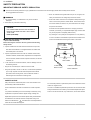
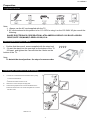
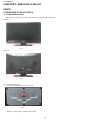
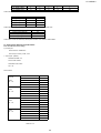
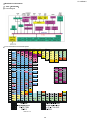
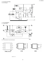
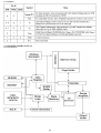
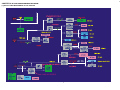
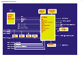
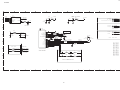
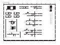
1
LC-42SB45U
SERVICE MANUAL
No S88T1LC42SB45
LCD COLOUR TELEVISION
MODEL
LC-42SB45U
In the interests of user-safety (Required by safety regulations in some countries) the set should be restored to its original condition and only parts identical to those specified should be used.
CONTENTS
SAFETY PRECAUTION
CHAPTER 6. BLOCK DIAGRAM/WIRING DIAGRAM
[1] MT5382 POWER MANAGEMENT BLOCK
DIAGRAM ................. ........................... ......... 56
[2] MAIN BOARD BLOCK DIAGRAM .................. 57
[3] WIRIGN DIAGRAM......................................... 58
IMPORTANT SERVICE SAFETY PRECAUTION ......................................................................2
Precautions for using lead-free solder ............. .............3
CHAPTER 1. OPERATION MANUAL
[1] SPECIFICATIONS ............................................... 4
[2] OPERATION MANUAL ........................................ 5
[3] DIMENSIONS ...................................................... 11
CHAPTER 7. PRINTED WIRING BOARD
[1] MAIN UNIT PRINT WIRING BOARD......... .. .......59
[2] POWER UNIT PRINT WIRING BOARD ...............61
[3] KEY UNIT PRINTED WIRINGBOARD........ .. ..... 63
[4] IR UNIT PRINTED WIRING BOARD ........... .. .....64
CHAPTER 2. REMOVING OF MAJOR PARTS
[1] REMOVING OF MAJOR PARTS ........................12
CHAPTER 8. SCHEMATIC DIAGRAM
[1] MAIN SCHEMATIC DIGRAM ................................65
[2] POWER SCHEMATIC DIGRAM ............................79
[3] KEY SCHEMATIC DIGRAM...... ...... ...... ...... ........80
[4] IR SCHEMATIC DIGRAM...... ...... ...... ...... ...... .....81
CHAPTER 3. ADJUSTMENT PROCEDURE
[1] ADJUSTMENT PROCEDURE .............................17
[2]CSM MODE............... ..........................................27
[3]FACTORY MODE.................................................28
[4]SOFTWARE UPGRADE PRODUCE...................28
CHAPTER 4. TROUBLESHOOTING TABLE
[1] TROUBLESHOOTING TABLE.............................33
CHAPTER 9. PARTS GAUILD
[1] SPARE PARTS LIST... ...... .... ... ...... .... ... ...... ....82
[2] CABINET PARTS ............................... ... ...... .... ... 108
[3] SUPPLIED ACCESSORIES... ...... .... ... ...... .... ... .109
[4] PACKING PARTS... ...... .... ... ...... .... ... ...... .... ... .110
CHAPTER 5. MAJOR IC INFORMATIONS
[1] MAJOR IC INFORMATIONS............................... 40
[2]MAJORICINFORMATION................................. ....40
[3] DETAILICsINFORMATION ..................................49
Parts marked with "
" are important for maintaining the safety of the set. Be sure to replace these parts with specified ones for maintaining the
safety and performance of the set.
This document has been published to be used for
after sales service only.
The contents are subject to change without notice.
1
LC-42SB45U
SAFETY PRECAUTION
IMPORTANT SERVICE SAFETY PRECAUTION
■
Service work should be performed only by qualified service technicians who are thoroughly familiar with all safety checks and the
servicing guidelines which follow:
• Use an AC voltmeter having with 5000 ohm per volt, or higher, sen-
■ WARNING
sitivity or measure the AC voltage drop across the resistor.
• Connect the resistor connection to all exposed metal parts having a
1. For continued safety, no modification of any circuit should be
attempted.
return to the chassis (antenna, metal cabinet, screw heads, knobs
2. Disconnect AC power before servicing.
and control shafts, escutcheon, etc.) and measure the AC voltage
drop across the resistor.
CAUTION:
All checks must be repeated with the AC cord plug connection
FOR CONTINUED PROTECTION AGAINST A
RISK OF FIRE REPLACE ONLY WITH SAME
TYPE FUSE.
reversed. (If necessary, a nonpolarized adaptor plug must be used
only for the purpose of completing these checks.)
Any reading of 1.05 V peak (this corresponds to 0.7 mA peak AC.)
F7000 (6.3A/250V)
or more is excessive and indicates a potential shock hazard which
■ BEFORE RETURNING THE RECEIVER
must be corrected before returning the monitor to the owner.
(Fire & Shock Hazard)
Before returning the receiver to the user, perform the following
safety checks:
DVM
3. Inspect all lead dress to make certain that leads are not pinched,
AC SCALE
and check that hardware is not lodged between the chassis and
1.5k ohm
other metal parts in the receiver.
10W
4. Inspect all protective devices such as non-metallic control knobs,
insulation materials, cabinet backs, adjustment and compartment
covers or shields, isolation resistor-capacitor networks, mechanical
0.15 µF
insulators, etc.
TEST PROBE
5. To be sure that no shock hazard exists, check for leakage current in
the following manner.
TO EXPOSED
• Plug the AC cord directly into a 220~240 volt AC outlet.
METAL PARTS
• Using two clip leads, connect a 1.5k ohm, 10 watt resistor paralleled
CONNECT TO KNOWN
EARTH GROUND
by a 0.15µF capacitor in series with all exposed metal cabinet
parts and a known earth ground, such as electrical conduit or
electrical ground connected to an earth ground.
//////////////////////////////////////////////////////////////////////////////////////////////////////////////////////////////////////////////////////////////////////////////////////////////////////////////////////////////////////////////////
SAFETY NOTICE
Many electrical and mechanical parts in LCD color television have
For continued protection, replacement parts must be identical to those
special safety-related characteristics.
used in the original circuit.
These characteristics are often not evident from visual inspection,
The use of a substitute replacement parts which do not have the same
nor
safety characteristics as the factory recommended replacement parts
can protection afforded by them be necessarily increased by using
shown in this service manual, may create shock, fire or other hazards.
replacement components rated for higher voltage, wattage, etc.
Replacement parts which have these special safety characteristics
are identified in this manual; electrical components having such
features are identified by “ ” and shaded areas in the Replacement
Parts List and Schematic Diagrams.
//////////////////////////////////////////////////////////////////////////////////////////////////////////////////////////////////////////////////////////////////////////////////////////////////////////////////////////////////////////////////
2
LC-42SB45U
Precautions for using lead-free solder
Employing lead-free solder
• “PWBs” of this model employs lead-free solder. The LF symbol indicates lead-free solder, and is attached on the PWBs and service manuals.
The alphabetical character following LF shows the type of lead-free solder.
Example
Indicates lead-free solder of tin, silver and copper.
Indicates lead-free solder of tin, silver and copper.
■ Using lead-free wire solder
• When fixing the PWB soldered with the lead-free solder, apply lead-free wire solder. Repairing with conventional lead wire solder may cause
damage or accident due to cracks.
As the melting point of lead-free solder (Sn-Ag-Cu) is higher than the lead wire solder by 40 °C, we recommend you to use a dedicated soldering
bit, if you are not familiar with how to obtain lead-free wire solder or soldering bit, contact our service station or service branch in your area.
Soldering
• As the melting point of lead-free solder (Sn-Ag-Cu) is about 220 °C which is higher than the conventional lead solder by 40 °C, and as it has
poor solder wettability, you may be apt to keep the soldering bit in contact with the PWB for extended period of time. However, Since the land
may be peeled off or the maximum heat-resistance temperature of parts may be exceeded, remove the bit from the PWB as soon as you
confirm the steady soldering condition.
Lead-free solder contains more tin, and the end of the soldering bit may be easily corroded. Make sure to turn on and off the power of the bit as
required.
If a different type of solder stays on the tip of the soldering bit, it is alloyed with lead-free solder. Clean the bit after every use of it.
When the tip of the soldering bit is blackened during use, file it with steel wool or fine sandpaper.
• Be careful when replacing parts with polarity indication on the PWB silk.
Lead-free wire solder for servicing
Part No.
ZHNDAi123250E
ZHNDAi126500E
ZHNDAi12801KE
★
J
J
J
Description
φ0.3mm 250g (1roll)
φ0.6mm 500g (1roll)
φ1.0mm 1kg (1roll)
Code
BL
BK
BM
3
LC-42SB45U
CHAPTER 1. OPERATION MANUAL
[1] SPECIFICATIONS
Specification
Item
Model:LC-42SB45U
LCD panel
a-si TFT LCD 42" Class
Resolution
2,073,600 pixels(1,920x1,080)
TV-standard(CCIR)
TV Function
Receiving
American TV standard ATSC/NTSC System
VHF/UHF
VHF 2-13ch,UHF 14-69ch
CATV
1-135ch(non-scrambled channel only)
Digital terrestrial
Channel
Broadcast(8VSB)
Digital cable
1-135ch(non-scrambled channel only)
(64/256QAM)
Audio multiplex
BTSC System
Backlight
60,000 hours(at Backlight standard position)
Audio out
10Wx2
Rear
Terminals
Side
INPUT 1
COMPONENT in,AUDIO in
INPUT 2
COMPONENT in,AUDIO in
INPUT 4
HDMI in with HDCP
INPUT 5
HDMI in with HDCP,Audio on(3.5mm jack)
INPUT 7
15-pin mini D-sub femal connector,Audio in(3.5mmjack)
ANT/CABLE
75 Unbalance,F Type x1 for Analog(VHF/UHF/CATV) and (AIR/CABLE)
DIGITAL AUDIO OUTPUT
Digital audio output x1(PCM/DOLBY Digital)
INPUT 3
AV in,S-VIDEO in
INPUT 6
HDMI in with HDCP
SERVICE
Software update
OSD language
English/French/Spanish
AC 120V,60Hz(For North America)
Power requirement
AC 110~240V,50-60Hz(For Others)
Power Consumption
Weight
220W(0.7W Standby with AC 120V)
TV+stand
48.72 lbs/22.1 kg
TV only
43.8 lbs/19.87 kg
Dimension
TV+stand
39.75x27.75x10.75 inch
(W xH xD)
TV only
39.75x27.62x3.88 inch
Operating temerature
•
2-69ch
+32°F to +104°F(0°C to +40°C)
As a part of policy of continuous improvement, SHARP reserves the right to make design and specification changes for product improvement
without prior notice. The performance specification figures indicated are nominal values of production units. There may be some deviations
from these values in individual units.
Optional accessory
The listed optional accessories are available for the LCD
colour TVs. Please purchase them at your nearest shop,
• Additional optional accessories may be available in the
No.
Part name
Part number
1
Wall mount bracket
AN-52AG4
near future. When purchasing, please read the newest
catalogue for compatibility and check the availability.
4
LC-42SB45U
[2] OPERATION MANUAL
Remote control unit
POWER:
Press to turn on/off the TV from on to standby mode, or inversely
DISPLAY:
Press to display information about the selected TV channel (Channel
banner)
INPUT:
1. Press repeatedly to select the signal source:
2. The Input List should be activated and show on OSD.
MUTE :
Interrupt the sound or restore it.
Number Key: 1. Press number button to direct access to TV channel
2. Press the pass code to activate the factory mode
3. Press to activate the Channel Lock (enter PIN code for Channel lock)
4. If channel list OSD active – jump to that channel in the channel list
(not tune the channel until OK is pressed)
- Dot key:
ENT:
Used for the digital channels
Used for accepting the key-in channel number
VOL +/ -:
Press to adjust the volume
CH +/ - :
1. Press to browse channels
2. Press to turn on TV from stand by mode
3. The channel number should appear on the set
FREEZE :
Frozen the current display
SURROUND : change audio mode (Mono/Stereo/Surround)
PLASHBACK: Press to alternate between the currently viewed program and previously
viewed program (It should return to previous view if it comes from
different signal source)
SLEEP:
Press to show the sleep-timer slider in the right side of screen. Press
displays current, subsequent presses advance (Loops)
MENU:
Press to activate OSD menu or exit OSD
2008-03-14
5
LC-42SB45U
TV (Front view)
TV (Rear view)
6
LC-42SB45U
Preparation
Supplied accessories
Note:
1.Always use the AC cord supplied with the TV.
2. AC cord enclosed in this product is for 110-125V.In using it on the 125-240V AC,pls consult the
following:
SHARP ELECTRONICS CORPORATION,LATIN AMERICA GROUP 6100 BLUE LAGOON
DRIVE,SUITE 150,MIAMI,FLORIDA 33126,U.S.A
Attaching/Detaching the TV Stand
Confirm that there are 4 screws supplied with the stand unit
1 Insert the stand into the openings on the buttom of the TV
2. ○
2. 2Insert and tighten the 4 screws into the 4 holes on the
○
buttom of the TV.
1.
Note:
To detach the stand,perform the steps in reverse order
Detaching the stand neck for Wall mounting
1.
1 Loosen the 4 screws that secure the stand neck by using
○
a cross-head screwdriver
2 Remove stand neck from the TV set.
○
2.
Loosen the 4 screws and pull out hinge plate
3.
1 Place the hinge plate in the TV set as illustration shown
○
2 Place the stand cover in the TV set and tighten the 4 screws
○
Into the 4 holes
2008-03-14
7
LC-42SB45U
preparation
installation of batteries in the Remote Control Unit
If the remote control fail to operate TV functions,replace the batteries in the remote control unit
1.
Open the battery cover .
2. Inser t two “AA “ size batteries
3. Close the battery cover
(supplied with the product)
.Place the batteries with their terminals
Corresponding to the (+) and (-)
Indications in the battery compartment
CAUTUION
Improper use of batteries can result in chemical leakage or explosion. Be sure to follow the instructions below.
1.Do not mix batteries of different types. Different types of batteries have different characteristics.
2.Do not mix old and new batteries. Mixing old and new batteries can shorten the life of new batteries or cause chemical leakage in old batteries.
3.Remove batteries as soon as they are worn out. Chemicals that leak from batteries that come in contact with skin can cause a rash. If you find
any chemical leakage, wipe thoroughly with a cloth.
4 The batteries supplied with this product may have a shorter life expectancy due to storage conditions.
5If you will not be using the remote control unit for an extended period of time, remove batteries from it.
using the remote control unit
Use the remote control unit by pointing it towards the
remote control sensor. Objects between the remote
control unit and sensor may prevent proper operation.
8
LC-42SB45U
Appendix
troubleshooting
Problem
possible Solution
No power
1.
Check if you pressed POWER on the remote control unit If the indicator
On the TV does not light up,pressPOWER on the TV.
2.
Is the AC cord disconnected?
3.
Has the power been turned on?
4.
External influence such as lighting ,static electricity,may cause improper
Operation.In this case,operate the unit after first turning off the power off the
TV or unplugging the AC cord and replugging it in after 1 or 2 minutes.
Unit cannot be operated
Remote control unit does no operate
1.
Is the FUNCTIOn set correctly? Set it to the TV setting position
2.
Are batteries inserted with polarity(+,-) aligned?
3.
Are batteries worn out ?(replace with new batteries)
4.
Is a fluorescent light illuminated near the remote control sensor?
5.
Are screen mode adjustments such as picture size made correctly?
Picture is cut off/with sidebar screen
Strange color,light color,or color misalignment
1.
Adjust the picture tone
2.
Is the room too right?The picture may look clark in a room that is
Too bright
3.
Check the input signal setting
4.
1.
Is the sleeptimer set?
2.
The unit’s internal temperature has increased.Remove any objects
Blocking vent or cleen
Powe r is suddenly turned off
No picture
1.
Is connection to other components correct?
2.
Is correct input signal source selected after connection?
3.
Is the correct input selected?
4.
Is picture adjustment correct?
5.
1.
Is the volume too low?
2.
Have you pressed MUTE on the remote control unit?
3.
This is not a malfunction.This happens when the cabinet slightly expands
and contracts according to change in temperature.This does not affect
the TV’s performance
No sound
The TV cometimes makes a creacking sound
Cautions regarding use in high and low temperature environments
• When the unit is used in a low temperature space (e.g. room, office), the picture may leave trails or appear slightly delayed. This
is not a malfunction, and the unit will recover when the temperature returns to normal.
• Do not leave the unit in a hot or cold location. Also, do not leave the unit in a location exposed to direct sunlight or near a
heater, as this may cause the cabinet to deform and the LCD panel to malfunction.
• Storage temperature: +5°C to +35°C.
information on the software license for this product
Software composition
The software included in this product is comprised of various software components whose individual copyrights
are held by SHARP or by third parties.
Software developed by SHarp and open source software
The copyrights for the software components and various relevant documents included with this product that
were developed or written by SHARP are owned by SHARP and are protected by the Copyright Act, international
treaties, and other relevant laws. This product also makes use of freely distributed software and software
components whose copyrights are held by third parties. These include software components covered by a GNU
General Public License (hereafter GPL), a GNU Lesser General Public License (hereafter LGPL) or other license
Agreement.
obtaining source code
Some of the open source software licensors require the distributor to provide the source code with the executable
software components. GPL and LGPL include similar requirements. For information on obtaining the source code
for the open source software and for obtaining the GPL, LGPL, and other license agreement information, visit the
following website:
2008-03-14
http://www.sharp-eu.com/gpl/
9
LC-42SB45U
We are unable to answer any questions about the source code for the open source software. The source code for
the software components whose copyrights are held by SHARP is not distributed.
acknowledgements
The following open source software components are included in this product:
•linuxkernel•modutils•glibc•zlib•libpng
10
LC-42SB45U
[3] DIMENSIONS
2008-03-14
11
LC-42SB45U
CHAPTER 2. REMOVING OF MAJOR
PARTS
[1] REMOVING OF MAJOR PARTS
1.Assy/Panel removal
Note :Please put your mechine on soft material to avoid to scrape panel when disassembly
Front View
Fig.1
Back View
Fig.2
Step 1.Remove the base assy
A, Remove 4screws as fig 3 and put out the base.
Fig 3
B.Remove 4 screws as Fig 4 to detach the base stand.
12
LC-42SB45U
Fig 4
Step 2.Remove the Back cover assy.
Remove 15 screws as Fig 5.
Fig 5
Step3.Remove the Power board.
Remove 5 screws and unplug 3 cables as Fig 6
2008-03-14
Fig.6
13
LC-42SB45U
Step 4.Remove the Scaler bard.
Remove 4 screws and unplug 6 cables as Fig.7
Fig 7
Step 5. Remove the Speaker(L/R)
Remove 4 screws as Fig 8 and Fig 9
Fig 8
Fig 9
Step 6. Remove the IR board
Remvoe 1 screws and unplug 1 cable as Fig 10
Fig 10
Step 7. Remove the Key board.
Unplug 1 cable as Fig 11
14
LC-42SB45U
Fig 11
Step 8.Remove the matel frame.
Remove 16 screws as Fig 12
Fig 12
Step 9. Remvoe the Front cover assy.
Remove 6 screws as Fig 13
Fig 13
2008-03-14
15
LC-42SB45U
Step 10.Panel picture
The panel Picture as Fig 14
Fig 14
2. Set Re-assembly
To re-assemble the whole set, execute all processes in reverse order.
Notes:
a. While re-assembling, make sure that all cables are placed and connected in their original position.
b. Pay special attention not to damage the EMC foams at the SSB shielding. Check that EMC foams are put
correctly on their places.
16
LC-42SB45U
CHAPTER 3. ADJUSTMENT PROCEDURE
PROCEDURE
[1] ADJUSTMENT PROCEDURE
1 OSD MENU
OSD tree - As following
z
TV
OSD Menu
Layer1
Layer2
Layer3
Layer4
SETTINGS
Picture
Contrast
slider(0-100)
Brightness
slider(0-100)
Color
slider(0-100)
Sharpness
slider(0-7)
Color temperature
Normal
Warm
Cool
Tint
slider(-7~7)
Active contrast
Off
On
View mode
Automatic
Smart stretch (Super zoom)
Side bar
(4:3)
Zoom
(Movie expand 16:9)
16:9 subtitle
Stretch
(Wide screen)
Audio
Audio setting
slider
Audio mode
Mono
Stereo
Virtual surround
Alternate audio
2008-03-14
Main
SAP
17
Layer5
LC-42SB45U
Digital audio language
AVL
Off
On
Features
Closed captions
Off
On
On during mute
Caption service
CC-1
CC-2
CC-3
CC-4
T-1
T-2
T-3
T-4
Digital caption service
CS-1
CS-2
CS-3
CS-4
CS-5
CS-6
Digital caption options
Reset to default
Reset to default
Size
Default
Small
Standard
Large
Text
Color
Default
Black
White
Red
Green
Blue
Yellow
Magenta
Cyan
Opacity
Default
Solid
Transparen
Translucen
Flashing
Background
Color
Default
Black
18
LC-42SB45U
White
Red
Green
Blue
Yellow
Magenta
Cyan
Opacity
Default
Solid
Transparen
Translucen
Flashing
Edge
Color
Default
Black
White
Red
Green
Blue
Yellow
Magenta
Cyan
Type
Default
None
Raised
Depressed
Outline
Left
shadow
Right
shadow
Sleep timer
slider(0-180)
Parental
control
Channel lock
(Please enter your PIN)
US TV ratings lock
(Please enter your PIN)
US Movie ratings lock
(Please enter your PIN)
Canada English ratings lock
(Please enter your PIN)
Canada French ratings lock
(Please enter your PIN)
Region ratings lock
(Please enter your PIN)
Set PIN / Change PIN
2008-03-14
(Please enter your current PIN)
Setup
19
LC-42SB45U
Language
English
Francais
Espanol
Auto CH search
Air
Cable
Start now
(Analog first then Digital)
Input source
TV
INPUT 1
(AV1)
INPUT 2
(AV2)
INPUT 3
(Side AV)
INPUT 4
(HDMI 1)
INPUT 5
(HDMI 2)
INPUT 6
(HDMI 3)
INPUT 7
(PC)
Clock
Enter Time
(Hrs,Mins,AM/PM)
Favorite channels (Only in
TV)
A
(Select channel)
B
(Select channel)
C
(Select channel)
D
(Select channel)
All data clear
Start now
Current software info
(Current software Version)
Reset
Start now
z
PC
OSD Menu
Layer1
Layer2
Layer3
Layer4
SETTINGS
Picture
Contrast
slider(0-100)
Brightness
slider(0-100)
Color temperature
Normal
20
Layer5
LC-42SB45U
Warm
Cool
View mode
Stretch (Full screen)
Dot by Dot
Audio
Audio setting
slider
Surround
Off
On
Setup
Language
English
Francais
Espanol
Input source
TV
INPUT 1
INPUT 2
INPUT 3
INPUT 4
INPUT 5
INPUT 6
INPUT 7
(AV1)
(AV2)
(Side AV)
(HDMI 1)
(HDMI 2)
(HDMI 3)
(PC)
Picture Adjustment
Auto adjust
Start
Manual adjust
Phase
Clock
Horizontal
Vertical
Reset
Start now
2008-03-14
21
LC-42SB45U
2. Picture check
1) WHITE-D adjustment
General set-up :
Equipment Requirements: Minolta CA-110 or Equivalent Color analyzer Chroma 2250 or equivalent PC signal generator input requirements:
Input Signal Type : PC VGA signal
1024X768/60Hz PC mode with ”5 white block” pattern. (see pattern-1)
Input Signal Strength : 0.7 Vp-p linear voltage.
Input Injection Point : PC D-SUB input
Pattern-1
Alignment method:
Initial Set-up:
1. Select source as “PC”.
2. Set Contrast = 50 (CMO) and Brightness=50 (CMO) , at normal menu mode.
3. Apply “5 white block”(pattern-1) pattern by VGA pattern generator.
4. Enter factory mode menu: Numeric keys “062596” + “Display” key (FAC mode menu). Then select “Factory” item.
Alignment:
1. At FAC mode menu, select AUTO_COLOR item. Then press “OK” key to adjust ADC_GAIN_R, ADC_GAIN_G,
ADC_GAIN_B and ADC_OFFSET_R, ADC_OFFSET_G, ADC_OFFSET_B. Then store those values to NVM.
2. Apply Flat80 pattern (80% white pattern).
3. Set color temperature to “NORMAL”.
4. At FAC mode menu, adjust the CLR TEMP R, CLR TEMP G, CLR TEMP B values to meet “NORMAL” color coordinates
specification below. Then store those values to NVM
3. Set color temperature to “COOL”.
4. At FAC mode menu, adjust the CLR TEMP R, CLR TEMP G, CLR TEMP B values to meet “COOL” color coordinates
specification below. Then store those values to NVM
3. Set color temperature to “WARM”.
4. At FAC mode menu, adjust the CLR TEMP R, CLR TEMP G, CLR TEMP B values to meet “WARM” color coordinates
specification below. Then store those values to NVM
Color temperature Normal/Warm/Cool (x, y) co-ordinates specification:
Picture Mode
Normal (9000oK)
Cool (11500oK)
Normal (6500oK)
x
0.289±0.005
0.278±0.005
0.314±0.005
Table 5: Reading with Minolta CA-110.
Note:
1>. Use Minolta CA-110 for color coordinates and luminance check.
22
y
0.291±0.005
0.278±0.005
0.319±0.005
LC-42SB45U
2
2>. Luminance > 400 cd/m in the center of the screen when Brightness control at 100; Contrast control at 100 for CMO 26”, 32”, 42” panels.
2) YPbPr Mode display adjustment
White balance adjustment
General set-up :
Equipment Requirement: Minolta CA-110 or Equivalent Color analyzer
Quantum Data Pattern Generator 802G , 802BT or equivalent instrument
Input requirements:
Input Signal Type
: YPbPr signal
1. 720P mode, TVBar100 pattern by 802G or 802BT.
2. Select Smart picture to Personal mode and check the x, y data.
Input Signal Strength : 1 Vpp for Y signal ; 700 mVpp for Pb & Pr signal
Input Injection Point : AV1 YPbPr (RAC jack)
720P, TVBar100 pattern
Alignment method:
Initial Set-up:
1. Select source as “AV1”.
2. Set Smart picture as “Personal” and to be Contrast =50,
Brightness=50 , at normal menu mode.
3. Apply “TVBar100” pattern (with black & white bar )by signal generator.
4. Enter factory mode menu: press Numeric keys “062596” then perss Display key (FAC mode menu). Then select “Factory”
item.
Alignment:
1. At FAC mode menu, select AUTO_COLOR item. Then press “OK” key to adjust ADC_GAIN_R, ADC_GAIN_G,
ADC_GAIN_B and ADC_OFFSET_R, ADC_OFFSET_G, ADC_OFFSET_B. Then store those values to NVM.
2. Apply Flat_73 pattern or 75IRE pattern.
3. Set color temperature to “NORMAL”.
3. Copy CLR_TEMP_R, CLR_TEMP_G and CLR_TEMP_B values from “NORMAL” color temperature in Analog TV mode.
Check whether (x,y) color coordinates meet “NORMAL” color specification below. If color coordinates are out of
specification, fine-tune CLR_TEMP_R, CLR_TEMP_G and CLR_TEMP_B values. Then store those values to NVM. ( R/G/B
gain value <= 130 )
4. Set color temperature to “WARM”.
5. Copy CLR_TEMP_R, CLR_TEMP_G and CLR_TEMP_B values from “WARM” color temperature in Analog TV mode.
Check whether (x,y) color coordinates meet “WARM” color specification below. If color coordinates are out of specification,
fine-tune CLR_TEMP_R, CLR_TEMP_G and CLR_TEMP_B values. Then store those values to NVM. ( R/G/B gain value
<= 130 )
6. Set color temperature to “COOL”.
7. Copy CLR_TEMP_R, CLR_TEMP_G and CLR_TEMP_B values from “COOL” color temperature in Analog TV mode. Check
whether (x,y) color coordinates meet “COOL” color specification below. If color coordinates are out of specification, fine-tune
CLR_TEMP_R, CLR_TEMP_G and CLR_TEMP_B values. Then store those values to NVM. ( R/G/B gain value <= 130 )
Color temperature Normal/Warm/Cool (x, y) co-ordinates specification:
2008-03-14
Picture Mode
Normal (9000oK)
x
0.289±0.010
23
y
0.291±0.010
LC-42SB45U
WARM (6500oK)
COOL( 11000oK)
0.314±0.010
0.278±0.010
0.319±0.010
0.278±0.010
3) HDMI HDCP Key Download
1 HDCP Key Encryption
The handling of HDCP keys must be done in the most secure way.
The HDCP keys purchased / delivered from Digital Content Protection, LLC are first encrypted by MTK encryption software. Then the encrypted
keys are stored in secure room or secure PC in production line.
2 HDCP Key Downloading to Set
In production line PC, execute HDCP key programming software to load encrypted key data from secure room or secure PC to specific positions
of set’s NVM via UART interface of MT538x chip.
3 Test HDCP Key
3.1. Use QuantumData 802BT or equivalent instrument with HDCP test pattern to verify HDCP key loaded in the set. The “PASS” information will
be shown in the lower center block of the screen when HDCP key is correctly loaded.
3.2 Use DVD player Pioneer DVD player xxx or equivalent DVD player with HDMI output to verify HDCP key loaded in the set. The video should
be smoothly displayed when HDCP key is correctly loaded.
4) Preset NVM data
NVM (U301) data has to be preset data according following table.
• NVM file name description:
1. FL4 (project name)
2. CMO 42” (Panel type and size)
3. NVM_xxxx (finalize testing Date)
4. xxxx(checksum / 2bytes) for CMO 42” panel
1>. Factory mode preset.
· Default Values
VIRGIN_MODE
AGING_MODE
GAMMA_TABLE
COLOR_ENHANCE
SET_PIN
FINETUNE_EQ
ORT_MODE
Off
On
Off
On
Off
Off
On
Note:ORT_MODE is Off for outgoing and is On at production line.
VIRGIN_MODE is ON for outging and is Off at production line.
ADC_GAIN_R
ADC_GAIN_G
ADC_GAIN_B
ADC_OFFSET_R
ADC_OFFSET_G
ADC_OFFSET_B
YPbPr
48
48
48
64
64
64
Note: These above values will be changed after doing “AUTO_COLOR” at FAC mode menu.
CLR_TEMP_R
CLR_TEMP_G
CLR_TEMP_B
NORMAL
128
117
99
YPbPr
WARM
135
110
71
COOL
128
121
115
Note: These above values will be changed after doing W/D alignment at FAC mode menu
24
LC-42SB45U
SP_MODE_3DNR
Personal
3
Sports
3
Standard
3
Movie
4
Power Saver
4
SP_MODE_PWM
15
15
15
15
120
These above values are defined by Development Division and written in SW code
SP_GAIN_BRI
YPbPr
123
SP_GAIN_CNT
128
SP_GAIN_TINT
32
SP_GAIN_CLR
142
These above values are defined by Development Division and written in SW code.
VIDEO_PWM_NORMAL
VIDEO_PWM_MEDIUM
VGA_PWM_MIN
15
120
200
VGA_PWM_MAX
15
These above values are defined by Development Division and written in release NVM.
2>. Smart picture & Smart sound & Feature
Final TV mode out of box setting.
a). Picture part :
Picture Format : Widescreen
Color Temp in Factory mode : Cool
b) Sound part : (default)
SOUND VOLUME : 20
Sound mode :Stereo
Alternative audio : Main
AVL : off
Smart Picture
Standard/
Personal
EQ BAND1
120Hz
0
EQ BAND2
500Hz
0
Stereo
AVL : off
EQ BAND3 1.5KHz
0
EQ BAND4
5KHz
2
EQ BAND5 10KHz
2
Sports
EQ BAND1
120Hz
2
Stereo
AVL : off
EQ BAND2
500Hz
2
EQ BAND3 1.5KHz
0
EQ BAND4
5KHz
-2
EQ BAND5 10KHz
-2
Movies
EQ BAND1
120Hz
8
Stereo
AVL : off
EQ BAND2
500Hz
4
EQ BAND3 1.5KHz
0
EQ BAND4
5KHz
4
Power saver
Stereo
AVL : off
EQ BAND5 10KHz
8
EQ BAND1
120Hz
6
EQ BAND2
500Hz
4
EQ BAND3 1.5KHz
0
EQ BAND4
5KHz
4
EQ BAND5 10KHz
6
2008-03-14
25
LC-42SB45U
Personal
Contrast
Brightness
50
Color
50
Sharpness
Color temperature
Tint
Picture format
Contrast
70
45
Color
65
Sharpness
5
0
Dynamic contrast
-wide
Contrast
50
Brightness
50
Color
50
Sharpness
4
Color temperature
normal
Tint
0
Dynamic contrast
--
Picture format
Contrast
wide
58
Brightness
50
Color
50
Sharpness
Color temperature
5
normal
Tint
0
Dynamic contrast
on
Picture format
Contrast
Power saver
normal
Tint
Picture format
Movie
-wide
Brightness
Color temperature
Standard
4
normal
0
Dynamic contrast
Sports
50
wide
55
Brightness
50
Color
50
Sharpness
Color temperature
2
normal
Tint
0
Dynamic contrast
--
Picture format
wide
c)Features:
Closed captions: Off
Caption service: CC-1
Digital caption service: CS1
Digital caption options: • Size :Large
• Style : Sans Serif
• Text : Color : Default
Opacity : Default
• Background : Color : Default
Opacity : Default
Sleeptimer: 0
26
LC-42SB45U
D) Installation:
Language: English
Clock: -- : -- AM
Current software info: TPV Version: FL4 ATSC Vx.xx.x yymmdd
[2] CSM MODE
How to Enter CSM mode method :
Step1: Press number key “123654” on remote control.
Step2: It will show CSM mode picture as below.
Step3: Press menu or volume up down key to exit CSM mode.
every item’s meaning as below :
Customer Service Menu 1
1:Set Type to be retrieved out of production -data
2: Production code 14 digit production -cde to be
retrieced per set to be written in NVM/EEPROm
3:SW-naming main-processor SW-naming of MSTAR
/Trident.see format in generic service document
4:SW-naming extra processor if valid
5:Code 1"Logging I2C errcodes in NVM/EEPROM
(5 last logged errors)
6:Code 2"Logging I2C errcodes in NVM/EEPROM
(5 last logged errors)
7:Key(HDCP)-HDMI information whehther
HDCP-Key is valid
8:Digital signal quality:(for Digital TV only)
9:NVM-naming :panel information
Error Code :
Error Code Type
TUNER
Error Code
3
Store to EEPROM
Yes
2008-03-14
27
LC-42SB45U
[3] FACTORY MODE
How to Enter factory mode menu:
1. Press Numeric keys “062596” + “Display” key (you should keep “Display” key until display below picture)(FAC
mode menu).
2. Scroll to the “Factory” selection and press “
model
”, then choose”start now” and press”ENTER”key to enter the factory
Start now
3.In the factory setting,press”
“and “
“ key to set the state that you want.
4.Press “Menu” to exit. or select “0” in the menu selection by up/down key then press enter.
Note: How to reset the factory setting?
1.Enter the facotry model(see page 28),then choose item 8 “VIRGIN_MODE” .
28
LC-42SB45U
2.Change the state from ”Off”” to “On” (By pressing “ ”key).
3. Press “Menu” to exit. or select “0” in the menu selection by up/down key then press “enter” .
4. Turn Power Off.
Then power on the set,you can find the factory settings has been OK.
2008-03-14
29
LC-42SB45U
[4] SOFTWARE UPGRADE PROCEDURE
Environment Setup
Before you start to write the code, we suggest you setup the environment first. This chapter lists the setup requirements
and guides you to setup and test your development environment.
Connect to ISP Board.
Use USB port connecting PC & MT537x Board via ISP board(Code number: 715G537XL2).
To PC USB port
To system board
service port
ISP tool
ISP tool
1. Unzip USB2COM Driver.zip to C:\
30
LC-42SB45U
PL-2303 Driver
Installer.zip
PL-2303 Driver
Installer.zip
PL-2303 Driver Installer.exe
2. Unzip USB2COM Driver.zip to C:\
Use MTK_Tools to download .bin file. (Ex: F4_dbg_image.bin or F4_image.bin)
3. Make sure the Type “MTK538X” && “USB Baud Rate 115200” && Load the correct “bin” file.
Load .bin file on the Linux system or on the local Windows file system(Ex: SHARP_ATSC_DLH_V0_34A_080714.bin) & Set
Bridge & Auto Set Flash BaudRate
4. Set COM port resource that used by USB Port.
2008-03-14
31
LC-42SB45U
5. Set Baud rate 115200 & High speed item Enable. & MT538x.
6. Push “Upgrade” button. (Waiting for “Finished!” message.)
Press “確定” button
7. Mainboard Power Off - On.
32
LC-42SB45U
CHAPTER 4. TROUBLESHOOTING TABLE
[1] TROUBLESHOOTING TABLE
Power unit operation check.
↓
Are the power cord and harness in the unit properly connected?
LINE_FILTER_UNIT:
NO
Connect the power cord and harness properly, and turn on the
power.
↓ YES
Is F901 normal?
NO
LINE_FILTER_UNIT:
Isn't L901,L902,RV902,C908,C909,C901,C902, etc. out of
order? Moreover, whether the short-circuit with the
circumference circuit is checked.
POWER_UNIT:
BD901, RV904, IC902, TH901, etc. out of order?
Moreover, whether the short-circuit with the circumference circuit
is checked.
POWER_UNIT
↓YES
Is BD901 (+320V) output? (Set the main power SW to OFF.)
NO
Does the PFC circuit operate normally?
(L903, L964, Q925, ZD914, D930, Q902, IC902 and etc. And,
the circuit around the protection circuit etc. is checked.)
NO
Does the switching circuit operate normally?
Check circuit around the primary side (T904, IC903, Q922,
Q924, ZD911, D924, D908, ZD910, etc.), the secondary side
(D927, L907, etc.), the AC_DET circuit (ZD912, ZD913, IC911,
IC913, Q918, IC909, Q915, etc.), and the protection circuit.
* When power on/off switch is on ‧‧‧ About +400V
↓YES
Is a voltage of +5V applied to pin (11,12) of connector (CN902)?
(Set the main power SW to OFF.)
↓YES
Are +24V output as for the power on/off switch when it is on?
NO
Does the inverter circuit operate normally?
Check circuit around the primary side (T905,Q920,Q919,IC901,
Q917,Q923,D936,D937,D932,ZD915,ZD916, etc.), the
secondary side (D901, D902, L906, L908, IC910, IC914, etc.),
the STANDBY circuit (Q915, etc.), and the protection circuit.
↓YES
Similarly, is +12V output as for the power on/off switch when it is
on?
NO
Check +12V circuit of D928, L909, etc.
The sound is not emitted from the speaker though the picture has come out.
↓
No sound output in all modes?
TEREMINAL UNIT:
↓
Is the audio signal output of pin (E26) (AL2) and pin (F25) (AR2) of
IC U400 normal?
NO
Check IC U400 and its peripheral circuits.
NO
Check the line between IC U400 and IC U600.
NO
Check the AMP_MUTE_LINE and POWERUP_LINE. (Q600,
etc.)
↓YES
Is audio signal input to pin (2)(L), pin (14)(R) of IC U600 (AMP)?
↓YES
Is MUTE circuit [AMP_MUTE_LINE, POWERUP_LINE] normal?
2008-03-14
↓YES
33
LC-42SB45U
NO
Is the audio signal output of pin (2, 1) (L-ch) and pin (1, 2) (R-ch) of
CN604 & CN605(AOUDIO-CONNECTOR) normal?
Check IC U600 and its peripheral circuits.
↓YES
Check Speaker (right and left) and wire harness.
No sound (during the reception of TV(ANALOG) broadcasting)
↓
Does not the sound go out though the picture has come out when UHF/VHF is received?
TEREMINAL UNIT:
↓
Is the SIF signal output from pin (3) of TUNER (TU201)?
NO
Check the tuner and its peripheral circuits. Replace as required.
NO
Check IC U400 its peripheral circuits.
↓YES
Is the SIF signal sent to pin (P25) and pin (P26) of IC U400?
↓YES
Refer to “No sound output in all modes”.
No sound (during the reception of TV (DIGITAL) broadcasting)
↓
Does not the sound go out though the picture has come out when DTV is received?
↓
MAIN UNIT:
NO
Is the DIF signal output from pin (18) and pin (19) of TUNER
(TU201)?
Check the tuner and its peripheral circuits. Replace as required.
↓YES
NO
Is the DIF signal sent to pin (AB24) and pin (AC24) of IC U400?
Check IC U400 its peripheral circuits.
↓YES
Refer to “No sound output in all modes”.
No sound from external input devices (1)
↓
Does not the sound of the audio signal input to INPUT 1(Component) go out?
Does not the sound of the audio signal input to INPUT 2(Component) go out?
MAIN UNIT:
↓
Is the audio signal properly sent to pin (2) (AV1_AudioLIN) and pin
(4)(AV1_AudioRIN) of CN552?
NO
Is the audio signal properly sent to pin (2) (AV2_AudioLIN) and pin
(4)(AV2_AudioRIN) of CN551?
Check the connection to CN552 and the external input device.
Check the connection to CN551 and the external input device.
↓YES
Is the audio signal properly sent to pin (J23) (AV1_LIN) and pin
(J24) (AV1_RIN) of IC U400?
Check the line between CN552 and IC U400.
NO
Is the audio signal properly sent to pin (J25) (AV2_LIN) and pin
(J26) (AV2_RIN) of IC U400?
Check the line between CN551 and IC U400.
↓YES
Refer to “No sound output in all modes”.
34
LC-42SB45U
No sound from external input devices (2)
↓
Does not the sound of the audio signal input to INPUT 3(Composite, Y/C) go out?
↓
MAIN UNIT:
Is the audio signal properly sent to pin (4) (AV3_AudioLIN) and pin
(6) (AV3_AudioRIN) of CN650?
NO
Check the connection to CN650 and the external input device.
↓YES
Is the audio signal properly sent to pin (K23) (AV3_LIN) and pin
(K24) (AV3_RIN) of IC U400?
NO
Check the line between CN650 and IC U400.
↓YES
Refer to “No sound output in all modes”.
No sound from external input devices (3)
↓
Does not the sound of the audio signal input to INPUT 7 (VGA) go out?
↓
MAIN UNIT:
Is the audio signal properly sent to pin (2) (VGA_AudioLIN) and pin
(3) (VGA_AudioRIN) of CN555?
NO
Check the connection to CN555 and the external input device.
↓YES
Is the audio signal properly sent to pin (K25) (VGA_LIN) and pin
(K26) (VGA_RIN) of IC U400?
NO
Check the line between CN555 and IC U400.
↓YES
Refer to “No sound output in all modes”.
No sound from external input devices (4)
↓
Does not the sound of the audio signal input to INPUT 4/5/6 (HDMI1/2/3) go out?
↓
Is picture of the signal input from INPUT 4/5/6 displayed?
NO
Refer to “Does not the picture of the HDMI signal input to
HDMI1/2/3 go out?”.
↓YES
Refer to “No sound output in all modes”.
The digital audio signal is not output (1)
↓
No digital audio signal output from SPDIF_OUTPUT terminal.
TEREMINAL UNIT:
↓
Is ASPDIF audio signal output from pin (B22) of IC U400 to pin (6)
of connector CN553?
YES
↓NO
Check IC U400 and its peripheral circuits.
2008-03-14
35
Check the connection to SPDIF_OUT and external devices.
LC-42SB45U
No picture on the display (1)
↓
The picture doesn't appear in all modes.
↓
MAIN UNIT:
Is LVDS signal output from 1st_channel and 2nd_channel of IC U400 in each mode?
(A0N/A0P),(A1N/A1P),(A2N/A2P),(A3N/A3P),(CLK1N/CLK1P),(A4N/A4P),(A5N/A5P),(A6N/A6P),(A7N/A7P),(CLK2N/CLK2P)
↓NO
Check IC U400 and its peripheral control circuits.
YES
Is the above-mentioned LVDS signals output to connector CN750?
NO
Check the line between IC U400 and CN750.
↓YES
Is LCD controller's control signal normal?
NO
Control signals BRIGHT_ADJ, INVERTER_ON_OFF,
PANEL_VCC_ON/OFF, and it peels off and whether normality is
checked.
NO
Wire harness is checked.
↓YES
PANEL_UNIT:
Similarly, is the LVDS signal input to connector of the panel
module?
↓YES
Check the panel module.
No picture on the display (2)
↓
Does not the picture come out when VHF/UHF is received?
↓
TERMINAL UNIT:
Is TUNER_CVBS signal output from pin (4) of TUNER (TU201)?
NO
Check whether I2C is normally accessed between TU201 and IC
U400.
↓YES
MAIN_UNIT:
Is picture signal input from pin (4) of TUNER (TU201) to pin (AC26)
of IC U400?
NO
Check the line between IC U400 and TU201.
↓YES
Refer to “The picture doesn't appear in all modes.”
No picture on the display (3)
↓
Does not the picture come out when DTV is received?
TERMINAL UNIT:
↓
Is the voltage of regulation for a TUNER circuit and the power
supply terminal of Q103 supplied?
NO
Each power supply circuit is checked.
NO
Check the tuner, IC U400 and their peripheral circuits. Replace
as required.
↓YES
Is IF signal output from pin (18), (19) of TUNER (TU201) to pin
(AB24), pin (AC24) of IC U400?
TERMINAL UNIT:
↓YES
Similarly, is communication control carried out between pin
(12)(SCL), pin(13)(SDA), pin(16)(AGC) of TU201?
MAIN_UNIT:
Do X300 (60.00MHz) oscillate?
NO
↓YES
NO
36
Check X300 and its peripheral circuits.
LC-42SB45U
↓YES
Refer to “The picture doesn't appear in all modes.”
<External input 1 / input 2 (Component)>No picture on the display (4)
↓
Does not the picture of the component video signal input (INPUT 1) to Component go out?
Does not the picture of the component video signal input (INPUT 2) to Component go out?
↓
TERMINAL_UNIT:
Is Component Y/Pb/Pr signal sent to pin (2)/Y, (4)/Pb, (6)/Pr of
AV1(CN552) ?
NO
Check the setting of an external input device that connects of
CN552.
Is Component Y/Pb/Pr signal sent to pin (2)/Y, (4)/Pb, (6)/Pr of
AV1(CN551) ?
NO
Check the setting of an external input device that connects of
CN551.
Is Component Y/Pb/Pr signal sent to pin (AD19)/Y, (AF20)/Pb,
(AD20)/Pr of IC U400?
NO
Check the line between IC U400 and CN552
Is Component Y/Pb/Pr signal sent to pin (AE21)/Y, (AE22)/Pb,
(AE23)/Pr of IC U400?
NO
Check the line between IC U400 and CN551.
↓YES
MAIN_UNIT:
↓YES
Refer to “The picture doesn't appear in all modes.”
<External input AV3 input 3 (Composite)>No picture on the display (5)
↓
Does not the picture of the composite video signal input to AV3(Composite) go out?
↓
TERMINAL UNIT:
NO
Is CVBS signal sent to pin (2) of AV3 (CN650) ?
Check the setting of an external input device that connects of
CN650.
↓YES
MAIN_UNIT:
NO
Is CVBS signal sent to pin (AD26) of IC U400?
Check the line between IC U400 and CN650.
↓YES
Refer to “The picture doesn't appear in all modes.”
<External input AV3 input 3 (Y/C)>No picture on the display (6)
↓
Does not the picture of the Y/C video signal input to AV3(Y/C) go out?
TERMINAL UNIT:
↓
Is Y/C signal sent to pin (8)/Y, (7)/C of AV3 (CN650) ?
NO
Check the setting of an external input device that connects of
CN650.
↓YES
MAIN_UNIT:
2008-03-14
Is Y/C signal sent to pin (AD25)/Y, (AE26)/C of IC U400?
NO
37
Check the line between IC U400 and CN650.
LC-42SB45U
↓YES
Refer to “The picture doesn't appear in all modes.”
<External input HDMI1 input 4 >No picture on the display (7)
↓
Does not the picture of the HDMI signal input to HDMI1 go out?
↓
MINI AV_UNIT:
Is the HOT_PLUG detection function of pin (19) of a HDMI terminal
(CN702) normal?
NO
Check the line between pin (AE1) of IC U400 and CN702.
↓
Check the connection and setup with the external HDMI devices.
YES
Are EDID data pin (6)(SCL) of IC U708 (EEPROM), pin (5)(SDA)
accessed, and is it read from pin (15), pin (16) of a HDMI
terminal(CN702)?
NO
Is access possible in the re-writing or exchange of EDID data of
IC U708?
↓NO
YES
Check CN702, IC U708 and peripheral circuits.
Is TMDS signal input into pin (AF7, AE7)/RX2±, (AF6, AE6)/RX1±,
(AF5, AE5)/RX0±, (AF4, AE4)/RXC± of IC U400?
NO
Check the line between IC U400 and CN702.
↓YES
Refer to “The picture doesn't appear in all modes.”
<External input HDMI2 input 5 >No picture on the display (8)
↓
Does not the picture of the HDMI signal input to HDMI2 go out?
↓
MINI AV_UNIT:
Is the HOT_PLUG detection function of pin (19) of a HDMI terminal
(CN700) normal?
NO
Check the line between pin (B20) of IC U400 and CN700.
↓
Check the connection and setup with the external HDMI devices.
YES
Are EDID data pin (6)(SCL) of IC U701 (EEPROM), pin (5)(SDA)
accessed, and is it read from pin (15), (16) of a HDMI
terminal(CN700)?
NO
Is access possible in the re-writing or exchange of EDID data of
IC U701?
↓NO
YES
Check CN700, IC U701 and peripheral circuits.
Is TMDS signal input into pin (AF11, AE11)/RX2±, (AF10,
AE10)/RX1±, (AF9, AE9)/RX0±, (AF8, AE8)/RXC± of IC U400?
NO
Check the line between IC U400 and CN700.
↓YES
Refer to “The picture doesn't appear in all modes.”
<External input HDMI3 input 6 >No picture on the display (9)
↓
Does not the picture of the HDMI signal input to HDMI3 go out?
38
LC-42SB45U
↓
MINI AV_UNIT:
Is the HOT_PLUG detection function of pin (19) of a HDMI terminal
(CN701) normal?
NO
Check the line between pin (AA4) of IC U400 and CN701.
↓
Check the connection and setup with the external HDMI devices.
YES
Are EDID data pin (6)(SCL) of IC U700 (EEPROM), pin (5)(SDA)
accessed, and is it read from pin (15), (16) of a HDMI
terminal(CN701)?
NO
Is access possible in the re-writing or exchange of EDID data of
IC U700?
↓NO
YES
Check CN701, IC U700 and peripheral circuits.
Is TMDS signal input into pin (AF15, AE15)/RX2±, (AF14,
AE14)/RX1±, (AF13, AE13)/RX0±, (AF12, AE12)/RXC± of IC U400?
NO
Check the line between IC U400 and CN701.
↓YES
Refer to “The picture doesn't appear in all modes.”
<External input VGA>No picture on the display (10)
↓
Does not the picture of the PC IN(ANALOG) video signal input to VGA input 7 (15pin-D-SUB terminal) go out?
TERMINAL_UNIT:
↓
Is R/G/B/H/V signal sent to pin (1)/R, (2)/G, (3)/B, (14)/H, (13)/V of
VGA (CN554)?
NO
Check the setting of an external input device that connects of
CN554.
↓YES
MAIN_UNIT:
Is R/G/B/H/V signal sent to pin (AE18)/R, (AE17)/G, (AF16)/B,
(AC16)/H, (AB17)/V of IC U400?
NO
↓YES
Refer to “The picture doesn't appear in all modes.”
2008-03-14
39
Check the line between IC U400 and CN554.
LC-42SB45U
CHAPTER 5. MAJOR IC INFORMATIONS
[1] Circuitry Description
1. General Description
This LCD-TV , FL4 support ATV NTSC / DTV ATSC (RF), YC, CVBS. Also for Y Pb Pr signal input from SDTV to HDTV (480i, 480p, 720p,
1080i/1080p 60Hz ).
This FL4 platform LCD - TV use Media Tech MT5382 IC , which has embedded ADC for HD/Analog D-sub input (no use ) , 3 digital port for HDMI
1.3 decoder digital data input , SD ADC for CVBS/YC input , video decoder , audio demodulator , audio decoder , audio DSP processing , USB 2.0
receiver , CC decoder , Microcontroller , OSD engine and up / down scaler .
MediaTek MT5382 is a highly integrated SOC ,which include Front –end demodulator , DTV backend decoder and TV controller. MT5382 support
transport de-multiplexer,MPEG-2 video decoder,AC3 audio decoder, LVDS transmitter, and TV decoder.
The MT5382 enables consumer electronics manufactures to build high quality, feature-rich DTV.
MT5382 embedded the MDDi de-interlacer to generate very smooth picture quality for motion. 3D com filter also recovery high detail for still picture.
The special color processing technology provides favorite and natural color for TV.
To enrich the features of DTV,MT5382 support HDMI receiver, integrated with high speed VGA ADC, high resolution Video/Audio ADC, 90dB Audio
DAC and 12-bit Video DAC. It will provide very fine quality for TV.
2. Feature Description
The combo tuner support both NTSC and ATSC RF signal ,
For the analog part , it build in analog video demodulator , decode the analog RF signal to CVBS , and deliver this CVBS signal to MT5382 for further
video processing . and at the same time deliver the 2nd IF signal , fed to MT5382 for audio demodulator and further audio processing .
For Digital part , It also deliver IF signal , fed to MT5382 for further processing
MT5382 merge MT5112 channel decoder , it is designed to support 8 VSB in full compliance with ATSC terrestrial Digital Television Standard . its
basic function is to recover the digital data encoded into the broadcast signal , which include video and audio program information and ancillary data
service . the device outputs the demodulated data as a standard MPEG-2 transport stream in within parallel or serial format .
It also support free QAM with cable system
The MT5382 platform support different source :
AV1/AV2 support two YPbPr component inputs , they can support SD/HD format
Side AV support CVBS , YC signal share with same audio
HDMI support HDMI / DVI input , the DVI audio share with side AV connector
All the input source video signal will directly fed to MT5382 for video part further processing
MT5382 merge Codec IC , so the audio signal also will fed to MT5382 directly
, the audio signal fed to build in MUX , select and digitalize , then fed
these audio data to next block for audio processing
MT5382 also support DAC , it can transfer the processing digital audio data to analog signal then fed to audio amplifier . it need extra headphone
amplifier , in case need support headphone signal to earphone .
The MT5382 support dual channel LVDS signal , connect these LVDS signal to panel for display picture
[2] MAJOR IC INFORMATION
2.1 U400(MT5382 AR)
GENERAL DESCRIPTION
The MediaTek MT5382AR consists of a DTV front-end demodulator, a backend decoder and a TV controller and offers high integration for advanced
applications. It combines a transport de-multiplexer, a high definition MPEG-2 video decoder, an AC3 audio decoder, an LVDS transmitter, and an
NTSC/PAL/SECAM TV decoder with a 3D comb filter. The MT5382AR enables consumer electronics manufactures to build high quality, low cost and
feature-rich iDTVs.
World-Leading Audio/Video Technology: The MT5382AR family has built-in high resolution and high-quality audio codec. It includes MediaTek
MDDiTM de-interlace solution to generate very smooth picture quality for motions. A 3D comb filter added to the TV decoder recovers great detail for still
pictures.The special color processing technology provides natural, deep colors and true studio quality graphics.
Rich Features for High Value Products: The MT5382AR enables a true single-chip experience. It integrates high-quality HDMI1.3, high speed VGA
ADC,dual-channel LVDS, USB2.0 receiver and multi-media decoder.
Reliable Front-end Receiving Capability: Excellent adjacent and co-channel rejection capability grants customers never miss any wonderful stream.
40
LC-42SB45U
Professional error-concealment provides stable, smooth and mosaic-free video quality.
Key Features:
·ATSC demodulator
·An transport demultiplexer
·An MPEG2 video decoder
·An AC3 audio decoder
·HDMI1.3 receiver
·Audio codec
FEATURES
Host CPU
· ARM 926EJS
· 8K I-Cache and 8K D-Cache
· 4K Instruction TCM
· JTAG ICE interface
· Watch Dog timers
· Built-in CPI analyzer
Transport Demultiplexer
· Supports a serial or parallel transport stream input
· Supports ATSC, MPEG-2 transport stream input
· Supports DES/3-DES
·Up to 8-PID even/odd keys for descrambling
· Supports 32 PID filters and 32 section filters
· Supports positive/negative/mask section filtering
· Supports hardware CRC-32 check
· Supports PCR recovery function
· Supports a micro-processor for stream process and MPEG start code detection
MPEG2/JPEG Decoder
· Supports one MPEG-2 HD decoder
· MPEG MP@ML, MP@HL and MPEG-1 video standards
· The MT5382AR supports de-blocking filter
· The MT5382AR supports JPEG decode base-line JPEG file
2D Graphics
· Supports multiple color modes
· Point, horizontal/vertical line primitive drawings
· Rectangle fill and gradient fill functions
· Bitblt with transparent options
· Alpha blending and alpha composition Bitblt
· Stretch Bitblt
· Font rendering by color expansion
· YCbCr to RGB color space conversion
· Supports off-line scaler
OSD Plane
· Two linking list OSDs with multiple color mode and one of them has scaler
Video Plane
·Supports Video capture and over scan
·Flesh tone management
·gamma/anti-Gamma correction
·Color transient improvement(CTI)
·2D peaking
·Saturation/hue adjustment
·Brightness and contrast adjustment2008-03-14
·Black and white level extender
·Adaptive luma/Chroma managemeng
41
LC-42SB45U
·Automatic detect film or video source
· 3:2/2:2 pull down source detection
· The MT5382AR supports maximum 1920 width motion-adaptive de-interlace. The MT5382AR supports
excellent low angle image processing.
· Arbitrary ratio vertical/horizontal scaling of video, from 1/32X to 32X
· Advanced non-linear panorama scaling.
· Programmable zoom viewer
· Progressive or interlace scan output
· Supports alpha blending
· Dithering processing for flat panel display
· Frame rate conversion.
· The MT5382AR supports FHD panel and VGA dot-to-dot.
· Doesn’t support PIP/POP
LVDS
· Supports 6/8/10-bit one–channel or 6/8-bit dual-channel LVDS transmitter, speeding up to 75 MHz
· Built-in spread spectrum for EMI performance
· Programmable panel timing output
CVBS In
· On-chip 54 MHz 10-bit video ADC
·Supports PAL (B,G,D,H,M,N,I,Nc), NTSC, NTSC-4.43, SECAM
·Macrovision detection
· NTSC/PAL support 3D comb filter, SECAM supports 2D comb filter
· Built-in motion-adaptive 3D Noise Reduction
·VBI data slicer for CC/TT decoding
·Supports 2-S-Video.
·The MT5382AR supports 4-channel CVBS.
· Supports SCART connector
VGA In
· Supports VGA input up to UXGA 162 MHz
· Supports full VESA standards
Component Video In
·Supports two component video inputs
·Supports 480i / 480p / 576i / 576p / 720p / 1080i / 1080p
Audio line in interface
·The MT5382AR supports 1-bit line in data (two channels)
HDMI Receiver
· The MT5382AR supports mixed 3-channels of HDMI1.3, data rate can be up to 2.25 GHz
·EIA/CEA-861B
· CEC
Audio ADC
·The MT5382AR supports 14-channel (7 R/L pairs) analog audio input.
TV Audio demodulator
·Supports BTSC/EIA-J/A2/NICAM/PAL FM/SECAM world-wide formats
·Standard automatic detection
·stereo demodulation,SAP delodulation
·Mode slection (main/SAP/Stereo)
Audio DAC
· Four on-chip audio DACs (2 R/L pairs) support R/L channel and subwoofer outputs
DRAM Controller
· Supports 64 Mb to 512 Mb DDR DRAM devices
·The MT5382AR supports configurable 16/32-bit data bus interface. The 16-bit address offers up to 64 M
bytes space. The 32-bit address offers up to 128 M bytes space.
42
LC-42SB45U
·Supports DDR1-333, DDR1-400, DDR2-400, DDR2-533, DDR2-667
Audio DSP
·Supports Dolby Digital AC-3 decoding (ATSC)
· MPEG-1 layer I/II decoding (DVB)
· Dolby Prologic II
· Audio output: 7.1ch + 2ch (down mix)
· Pink noise and white noise generator
· Equalizer
· Bass management
· 3D surround processing with virtual surround
· Audio and video lip synchronization
·Supports reverberation
· Automatic volume control
·One SPDIF out
· The MT5382AR supports 5-bit (10-channel) main audio I2S output interface. Each channel is up to 24-bit
resolution.
· While internal audio DAC is disabled, the MT5382AR supports 1-bit (2-channel) aux audio I2S output I/F.
Each channel is up to 24-bit resolution.
Digital TV Demodulator
·Compliant with ATSC digital television standard
·Supports SCTE DVS-031 and ITU J.83 Annex B digital CATV standard
·Accepts direct IF (44 MHz or 43.75 MHz) and low IF (5.38 MHz)
·NTSC interference rejection capability
· Passes all Brazil fading channel ensembles
· Meets all ATSC/A74 requirements
·Excellent adjacent and co-channel rejection capability, only a single SAW is required
· Dual digital AGC controls for IF and RF, respectively
·Full-digital frequency offset recovery with wide acquisition range ±1 MHz for ATSC and ±250 kHz for
CATV reception
·EIA/CEA-909 antenna interface, both mode A, and mode B are supported
Analog TV IF Demodulator
·Supports NTSC M/N standard
·Accepts IF frequency at 45.75 MHz
·Full digital AGC control and carrier recovery
Periopherals
·MT5382 AR has two built-in dedicated UARTs with TxFIFO and one shared UART,one of them has hardware flow control and high speed data
transferring
·The MT5382AR has three basic serial interfaces;one is for the tuner ,one is the master for general purpose and the other is the slave for HDMI EDID
data.The MT5382AR has two extra slave serial interfaces used for the second and the third HDMI EDID data
·Three PWMs
·The MT5382AR supports up to 2 serial flash or 1 serial flash + 1 NAND flash.
· While NAND Flash is not enabled, the MT5382 AR supports xD/SM, MS/MS-PRO, SD/MMC, and SDHC
card reader.
·IR blaster and receiver
· Real-time clock and watchdog controller
·1-port USB2.0/1.1 host supports USB mass storage class devices.
· Supports five servo ADCs.
IC Outline
·The MT5382AR is 465-pin BGA package.
· 3.3V/1.0V and 2.5V for DDR1,1.5V for DDR2.
2008-03-14
43
LC-42SB45U
2.2 U102(LP2996MRX PSOP-8)
General Description
The LP2996 linear regulator is designed to meet the JEDEC SSTL-2 specifications for termination of DDR-SDRAM. The device contains a high-speed
operational amplifier to provide excellent response to load transients. The output stage prevents shoot through while delivering 1.5A continuous current
and transient peaks up to 3A in the application as required for DDR-SDRAM termination. The LP2996 also incorporates a VSENSE pin to provide superior
load regulation and a VREF output as a reference for the chipset and DIMMs. An additional feature found on the LP2996 is an active low shutdown (SD) pin
that provides Suspend To RAM (STR) functionality. When SD is pulled low the VTT output will tri-state providing a high impedance output, but, VREF will
remain active. A power savings advantage can be obtained in this mode through lower quiescent current.
Features
· Source and sink current
· Low output voltage offset
· No external resistors required
· Linear topology
· Suspend to Ram (STR) functionality
· Low external component count
· Thermal Shutdown
· Available in SO-8, PSOP-8 or LLP-16 packages
Applications
· DDR-I and DDR-II Termination Voltage
· SSTL-2 and SSTL-3 Termination
· HSTL Termination
23.U103/ U104 (L5985 VFQFPN8)
Description
The L5985 is a step down switching regulator with 2.5A current limited embedded power MOSFET, so it is able to deliver up to 2A DC current to the load
depending on the application condition.
The input voltage can range from 2.9V to 18V, while the output voltage can be set starting from 0.6V to VIN. Having a minimum input voltage of 2.9V, the
device is suitable for buses staring from for 3.3V bus.
Requiring a minimum set of external components, the device includes an internal 250KHz switching frequency oscillator that can be externally adjusted up
to 1MHz.
The QFN package with exposed pad allows reducing the RthJA down to approximately 60°C/W.
Features
· 2A DC output current
· 2.9V to 18V input voltage
· Output voltage adjustable from 0.6V
· 250KHz switching frequency, programmable up to 1MHz
·Internal Soft-start and Inhibit
· Low dropout operation: 100% duty cycle
· Voltage feed-forward
· Zero load current operation
· Over current and thermal protection
· VQFN3x3-8L package
Applications
· Consumer:
STB, DVD, DVD recorder, car audio, LCD TV and monitors
· Industrial:
Chargers, car battery, PLD, PLA, FPGA
· Networking: XDSL, modems, DC-DC modules
· Computer:
Optical storage, hard disk drive, printers, audio/graphic cards
2.4. U351/U352 (HYB18TC256160BF-3S TFBGA-84-55)
Features
The 256-Mbit Double-Data-Rate-Two SDRAM offers the following key features:
· 1.8 V ± 0.1 V Power Supply
· 1.8 V ± 0.1 V (SSTL_18) compatible I/O
· DRAM organizations with 4, 8 and 16 data in/outputs
· Double Data Rate architecture: two data transfers per clock cycle four internal banks for concurrent operation
· Programmable CAS Latency: 3, 4, 5 and 6
· Programmable Burst Length: 4 and 8
· Differential clock inputs (CK and CK)
· Bi-directional, differential data strobes (DQS and DQS) are transmitted / received with data. Edge aligned with read data and center-aligned with write
data.
· DLL aligns DQ and DQS transitions with clock
· DQS can be disabled for single-ended data strobe operation
44
LC-42SB45U
· Commands entered on each positive clock edge, data and data mask are referenced to both edges of DQS
· Data masks (DM) for write data
· Posted CAS by programmable additive latency for better command and data bus efficiency
· Off-Chip-Driver impedance adjustment (OCD) and On-Die-Termination (ODT) for better signal quality.
· Auto-Precharge operation for read and write bursts
· Auto-Refresh, Self-Refresh and power saving Power-Down modes
· Average Refresh Period 7.8 µs at a TCASE lower than 85 °C, 3.9 µs between 85 °C and 95 °C
· Programmable self refresh rate via EMRS2 setting
· Programmable partial array refresh via EMRS2 settings
· DCC enabling via EMRS2 setting
· Full and reduced Strength Data-Output Drivers
· 1K page size
· Packages: PG-TFBGA-84
1
· RoHS Compliant Products )
· All Speed grades faster than DDR400 comply with DDR400 timing specifications when run at a clock rate of 200 MHz.
2.5. U600 (TDA8932B)
General Description
The TDA8932B is a high efficiency class-D amplifier with low power dissipation.
The continuous time output power is 2 ´ 15 W in stereo half-bridge application (RL = 4 W) or 1 ´ 30 W in mono full-bridge application (RL = 8 W). Due to
the low power dissipation the device can be used without any external heat sink when playing music. Due to the implementation of thermal foldback, even
for high supply voltages and/or lower load impedances, the device remains operating with considerable music output power without
the need for an external heat sink.
The device has two full-differential inputs driving two independent outputs. It can be used
as mono full-bridge configuration (BTL) or as stereo half-bridge configuration (SE).
Features
·Operating voltage from 10 V to 36 V asymmetrical or ±5 V to ±18 V symmetrical
· Mono-bridged tied load (full-bridge) or stereo single-ended (half-bridge) application
· Application without heatsink using thermally enhanced small outline package
· High efficiency and low-power dissipation
·Thermally protected and thermal foldback
· Current limiting to avoid audio holes
·Full short-circuit proof across load and to supply lines (using advanced current
protection)
·Switchable internal or external oscillator (master-slave setting)
· No pop noise
· Full-differential inputs
Applications
·Flat panel television sets
·Flat panel monitor sets
·Multimedia systems
·Wireless speakers
· Mini and micro systems
· Home sound sets
2.6. U151 (LD1117DT33TR)
General description
The LD1117 is a LOW DROP Voltage Regulator able to provide up to 800mA of Output Current, available even in adjustable version (Vref=1.25V).
Concerning fixed versions, are offered the following Output Voltages: 1.2V,1.8V,2.5V,2.85V, 3.0V 3.3V and 5.0V. The 2.85V type is ideal for
SCSI-2 lines active termination. The device is supplied in: SOT-223, DPAK, SO-8, TO-220 and TO-220FM. The SOT-223 and DPAK surface
mount packages optimize the thermal characteristics even offering a relevant space saving effect. High efficiency is assured by NPN
pass transistor. In fact in this case, unlike than PNP one, the Quiescent Current flows mostly into the load. Only a very common 10µF minimum
capacitor is needed for stability. On chip trimming allows the regulator to reach a very tight output voltage tolerance, within ± 1% at 25°C. The
ADJUSTABLE LD1117 is pin to pin compatible with the other standard. Adjustable voltage regulators maintaining the better performances in
terms of Drop and Tolerance.
2.7. U153/U154 (LD1117DTTR) 2008-03-14
General description
45
LC-42SB45U
The LD1117 is a LOW DROP Voltage Regulator able to provide up to 800mA of Output Current, available even in adjustable version (Vref=1.25V).
Concerning fixed versions, are offered the following Output Voltages: 1.2V,1.8V,2.5V,2.85V, 3.0V 3.3V and 5.0V. The 2.85V type is ideal for
SCSI-2 lines active termination. The device is supplied in: SOT-223, DPAK, SO-8 and TO-220. The SOT-223 and DPAK surface mount packages optimize
the thermal characteristics even offering a relevant space saving effect. High efficiency is assured by NPN pass transistor. In fact in this case, unlike than
PNP one, the Quiescent Current flows mostly into the load. Only a very common 10µF minimum capacitor is needed for stability. On chip trimming allows
the regulator to reach a very tight output voltage tolerance, within ± 1% at 25°C. The ADJUSTABLE LD1117 is pin to pin compatible with the other
standard. Adjustable voltage regulators maintaining the better performances in terms of Drop and Tolerance.
Features
·Low dropout voltage (1V TYP.)
· 2.85V Device performances are suitable for SCSI-2 active termination
· Output current up to 800 mA
· Fixed output voltage of: 1.2V, 1.8V, 2.5V, 2.85V, 3.0V, 3.3V, 5.0V
· Adjustable version availability (Vrel=1.25V)
· Internal current and thermal limit
· Available in ± 1% (at 25°C) and 2% in full temperature range
·Supply voltage rejection: 75dB (typ.)
2.8. U721 (LD39080PT)
General Description
The LD39080 is a fast ultra low drop linear regulator which operates from 2.5V to 6V input supply. A wide range of output options are available. The
low drop voltage, low noise, and ultra low quiescent current make it suitable for low voltage microprocessor and memory applications. The device is
developed on a BiCMOS process which allows low quiescent current operation independently of output load current.
Features
·0.8A Guaranteed output current
· Ultra low dropout voltage (150mV typ. @ 0.8A load, 20mV typ. @150mA load)
·Very low quiescent current (1mA typ. @ 0.8A load, 1µA max @ 25°C in off mode)
·Logic-controlled electronic shutdown
· Current and thermal internal limit
· ±1.5% Output voltage tolerance @ 25°C
·Fixed and ADJ output voltages: 1.22V, 1.8V, 2.5V, 3.3V, ADJ.
·Temperature range: -40 to 125°C
· Fast dynamic response to line and load changes
· Stable with ceramic capacitor
· Available in PPAK, DPAK and DFN8 (4x4mm)
2.9. U701/U708/U700/U550(M24C02-WDW6P TSSOP8)
DESCRIPTION
These I²C-compatible electrically erasable programmable memory (EEPROM) devices are organized as 2048/1024/512/256/128 x 8 (M24C16, M24C08,
M24C04, M24C02 and M24C01).
In order to meet environmental requirements, ST offers these devices in ECOPACK® packages. ECOPACK® packages are Lead-free and RoHS
compliant.
ECOPACK is an ST trademark. ECOPACK specifications are available at: www.st.com.
I²C uses a two-wire serial interface, comprising a bidirectional data line and a clock line. The devices carry a built-in 4-bit Device Type Identifier code (1010)
in accordance with the I²C bus definition.
The device behaves as a slave in the I²C protocol, with all memory operations synchronized by the serial clock. Read and Write operations are initiated by
a Start condition, generated by the bus master. The Start condition is followed by a device select code and Read/Write bit (RW), terminated by an
acknowledge bit.
When writing data to the memory, the device inserts an acknowledge bit during the 9th bit time, following the bus master’s 8-bit transmission. When data is
read by the bus master, the bus master acknowledges the receipt of the data byte in the same way. Data transfers are terminated by a Stop condition after
an Ack for Write, and after a NoAck for Read.
.
FEATURES
· Two-wire I²C serial interface
46
LC-42SB45U
Supports 400 kHz protocol
· Single supply voltage:
– 2.5 V to 5.5 V for M24Cxx-W
– 1.8 V to 5.5 V for M24Cxx-R
– 1.7 V to 5.5 V for M24Cxx-F
· Write Control input
· Byte and Page Write (up to 16 bytes)
· Random and Sequential Read modes
· Self-timed programming cycle
· Automatic address incrementing
· Enhanced ESD/latch-up protection
· More than 1 million write cycles
·More than 40-year data retention
· Packages
– ECOPACK® (RoHS compliant)
2.10.U402 (MX25L3205DMI-12G SOP-16)
FEATURES
GENERAL
· Serial Peripheral Interface compatible -- Mode 0 and Mode 3
· 32M:33,554,432 x 1 bit structure or 16,772,216 x 2 bits (two I/O read mode) structure
· 1024 Equal Sectors with 4K byte each (32Mb)
- Any Sector can be erased individually
· 64 Equal Blocks with 64K byte each (32Mb)
- Any Block can be erased individually
· Single Power Supply Operation
- 2.7 to 3.6 volt for read, erase, and program operations
· Latch-up protected to 100mA from -1V to Vcc +1V
· Low Vcc write inhibit is from 1.5V to 2.5V
PERFORMANCE
• High Performance
- Fast access time: 86MHz serial clock (15pF + 1TTL Load) and 66MHz serial clock (30pF + 1TTL Load)
- Serial clock of two I/O read mode : 50MHz (15pF + TTL Load), which is equivalent to 100MHz
- Fast program time: 1.4ms(typ.) and 5ms(max.)/page (256-byte per page)
- Byte program time: 7us (typical)
- Continuously program mode (automatically increase address under word program mode)
- Fast erase time: 60ms(typ.) /sector (4K-byte per sector) ; 0.7s(typ.) /block (64K-byte per block); 25s(typ.) for 32Mb
· Low Power Consumption
- Low active read current: 25mA(max.) at 86MHz, 20mA(max.) at 66MHz and 10mA(max.) at 33MHz
- Low active programming current: 20mA (max.)
- Low active erase current: 20mA (max.)
- Low standby current: 20uA (max.)
- Deep power-down mode 1uA (typical)
· Typical 100,000 erase/program cycles
SOFTWARE FEATURES
· Input Data Format
- 1-byte Command code
· Advanced Security Features
- Block lock protection
The BP0-BP3 status bit defines the size of the area to be software protection against program and erase instructions
- Additional 512-bit secured OTP for unique identifier
· Auto Erase and Auto Program Algorithm
- Automatically erases and verifies data at selected sector
- Automatically programs and verifies data at selected page by an internal algorithm that automatically times the program pulse widths (Any page to be
programed should have page in the erased state first)
· Status Register Feature
· Electronic Identification
2008-03-14
- JEDEC 1-byte manufacturer ID and 2-byte device ID
47
LC-42SB45U
- RES command for 1-byte Device ID
- Both REMS and REMS2 commands for 1-byte manufacturer ID and 1-byte device ID
HARDWARE FEATURES
· SCLK Input
- Serial clock input
· SI Input
- Serial Data Input
· SO Output
- Serial Data Output
· WP#/ACC pin
- Hardware write protection and program/erase acceleration
· HOLD# pin
- pause the chip without diselecting the chip
· PACKAGE
- 16-pin SOP (300mil)
- 8-land WSON (8x6mm or6x5mm)
- 8-pin SOP (200mil, 150mil)
- 8-pin PDIP (300mil)
- All Pb-free devices are RoHS Compliant
48
LC-42SB45U
3. Detailed ICs Information
3.1. U400(MT5382 AR)
3.1.1 Block Diagram
3.1.2 Pin Connections and short description
2008-03-14
49
LC-42SB45U
3.2. U102 (LP2996MRX PSOP-8)
3.2.1 Pin Connections and short description
50
LC-42SB45U
3.3. U104/U103 (L5985 VFQFPN8)
3.3.1 Pin Connections and short description
N°
1
2
Type
OUT
SYNCH
3
INH
4
5
COMP
FB
6
FSW
7
8
GND
VCC
Description
Regulator output
Master/Slave Synchronization. When it is left floating, a signal with a phase shift of half a period respect to the power turn
on is present at the pin. When connected to an external signal at a frequency higher than the internal one, then the
device is synchronized by the external signal, with zero phase shift.
Connecting together the SYNC pin of two devices, the one with higher frequency works as master and the other one as
slave; so the two power turn on have a phase shift of half a period.
A logical signal (active high) disable the device. With INH higher than 1.9V the device is OFF and with INH lower than
0.6V the device is ON.
Error Amplifier output to be used for loop frequency compensation
Feedback input. Connecting the output voltage directly to this pin the output voltage is regulated at 0.6V. To have higher
regulated voltages an external resistor divider is required from Vout to FB pin.
The switching frequency can be increased connecting an external resistor from FSW pin and ground. If this pin is left
floating the deice works at its free-running frequency of 250KHz.
Ground
Unregulated DC input voltage
3.4. U351/U352 (HYB18TC256160BF-3S TFBGA-84-55)
3.4.1 Pin Connections and short description
Ball#/Pin#
Name
Data Signals ×16 Organization
G8
DQ0
G2
DQ1
H7
DQ2
H3
DQ3
H1
DQ4
H9
DQ5
F1
DQ6
F9
DQ7
C8
DQ8
C2
DQ9
D7
DQ10
D3
DQ11
D1
DQ12
D9
DQ13
B1
DQ14
B9
DQ15
Data Strobe ×16 Organization
B7
UDQS
A8
UDQS
F7
LDQS
Pin Type
Buffer Type
Function
I/O
I/O
I/O
I/O
I/O
I/O
I/O
I/O
I/O
I/O
I/O
I/O
I/O
I/O
I/O
I/O
SSTL
SSTL
SSTL
SSTL
SSTL
SSTL
SSTL
SSTL
SSTL
SSTL
SSTL
SSTL
SSTL
SSTL
SSTL
SSTL
Data Signal 15:0
SSTL
SSTL
SSTL
Data Strobe Upper Byte
2008-03-14
I/O
I/O
I/O
Data Strobe Lower Byte
51
LC-42SB45U
E8
LDQS
Data Mask ×16 Organization
B3
UDM
LDM
F3
Power Supplies ×16 Organization
J2
VREF
E9, G1, G3, G7, G9
VDDQ
J1
VDDL
E1, J9, M9, R1
VDD
E7, F2, F8, H2, H8
VSSQ
J7
VSSDL
A3, 3,J3,N1,P9
VSS
Not Connected ×16 Organization
A2, E2, L1, R3, R7, R8
NC
Other Pins ×16 Organization
K9
ODT
I/O
SSTL
I
I
SSTL
SSTL
Data Mask Upper/Lower Byte
AI
PWR
PWR
PWR
PWR
PWR
PWR
—
—
—
—
—
—
—
I/O Reference Voltage
I/O Driver Power Supply
Power Supply
Power Supply
I/O Driver Power Supply
Power Supply
Power Supply
NC
—
Not Connected
I
SSTL
On-Die Termination Control
3.5. U600 (TDA8932B)
3.5.1 Block diagram
3.5.1 Pin Connections and short description
52
LC-42SB45U
3.6. U151 (LD1117DT33TR)
3.6.1 Block Diagram
3.7. U721 (LD39080PT)
3.7.1 Block Diagram
3.7.2 Pin Connections and short description
2008-03-14
53
LC-42SB45U
3.8. U402 (MX25L3205DMI-12G SOP-16)
3.8.1 Block Diagram
54
LC-42SB45U
3.8.2
PIN CONFIGURATION
2008-03-14
55
LC-42SB45U
CHAPTER 6. BLOCK DIAGRAM/WIRING DIAGRAM
[1] MT5382 POWER MAGAGEMENT BLOCK DIAGRAM
56
LC-42SB45U
[2] MAIN BOARD BLOCK DIAGRAM
2008-03-14
57
LC-42SB45U
[3] WIRING DIAGRAM
58
LC-42SB45U
CHAPTER 7. PRINTED WIRING BOARD
[1] MAIN UNIT PRINTED WIRING BOARD
MAIN Unit (Side-A)
59
LC-42SB45U
MAIN Unit (Side-B)
60
LC-42SB45U
[1]POWER UNIT PRINTED WIRING BOARD
POWER Unit (Side-A)
61
LC-42SB45U
POWER Unit (Side-B)
62
LC-42SB45U
[3]KEY BOARD UNIT PRINTED WIRING BOARD
KEY BOARD Unit (Side-A)
KEY BOARD Unit (Side-A)
63
LC-42SB45U
[3]IR UNIT PRINTED WIRING BOARD
IR Unit (Side-A)
IR Unit (Side-A)
Cn001 A2
64
LC-42SB45U
CHAPTER 8.SCHEMATIC DIAGRAM
[1]MAIN SCHEMATIC DIAGRAM
1.Power-1
1
3
DLA/DJA MT538X
R142
L100
CN100 B1
C100 B4
C101 B9
C102 F2
C103 D9
C104 F5
C105 B8
C106 B4
C107 B5
C108 E3
C109 F4
C110 C6
C111 E6
C112 E1
C113 D4
C114 B8
C115 C5
C116 D8
C117 E9
C118 F9
C119 G9
C120 G9
C121 C8
C122 C6
C123 G10
C124 D2
C125 F3
C126 G8
C127 G8
C128 E5
C129 E2
C130 E6
C131 E1
C132 E4
C133 B9
C134 D9
C135 C2
C136 C2
C137 C8
C138 C7
C140 E8
FB100 C1
FB101 C1
L100 B5
L101 E2
L102 E5
Q100 G8
Q101 B8
Q102 E8
Q103 F7
Q104 B8
Q105 D9
Q106 D2
Q107 E7
Q108 F3
Q109 F4
Q110 C4
R100 G7
R101 G7
R102 G8
R103 G7
R104 E2
R105 B5
R106 E5
R107 B7
R108 B2
R109 C5
R110 C5
R111 D9
R112 B6
R113 B2
R114 F10
R115 E1
R116 E6
R117 F1
R118 B5
R119 B8
R120 F7
R121 B5
R122 F5
R123 E5
R124 E1
R125 E5
R126 D2
R127 F3
R128 F4
R129 D1
R130 B8
R131 F9
R132 G9
R133 B4
R134 B3
R135 E4
R136 E3
R137 E1
R138 D8
R139 E8
R140 D7
R141 E9
R142 B2
R143 F7
R144 D2
R145 C7
R146 D4
R147 D4
R148 C6
R149 D9
R150 E8
TP100 B1
TP101 B1
TP102 B1
TP103 B1
TP104 B1
TP105 B1
TP106 B1
U101 B4
U102 F10
U103 E4
U104 E3
ZD100 E5
ZD101 E2
ZD102 C5
NC/MUN2211TIG
ZD102
NC/SS2P4
Use new comp
C138 C137 C121
Reserved
R145
CEC_PWRSB
NC/10K 1/16W 5%
SMD/0402
CEC_PWRSB:
Normal: High
Stand_by: Low
MEM_VREF
VTT
GND
GND
5,7,9,12,13 DV33SB
DV33SB
+5V_STB(+5V4) TO +5V_SW
CEC_PWR(DV33SB ON/OFF):
Normal: Low
Stand_By: High
R146 NC/0R05 1/4W
CEC_PWR
6 MEM_VREF
6 VTT
10K 1/10W 5%
R148
NC/1K 1/10W
DV33
9 CEC_PWR
2,3,4,5,6,7,8,9,10,11,12,13,14
STAND_BY
BRIGHT_ADJ
INVERTER_ON_OFF
+3V3SB
2,9 +3V3SB
C114
NC/4.7UF 10V
+24V
+12V
+5V_STB
+5V_SW
+5V1_TUN
DV18_DDR
DV11
OPWRSB
NC/100N 16V
C122
NC/100N 50V
+24V or +12V TO +5V_STB(+5V4)_reserved for OTS42"
R144
NC/2K2 1/16W 5%
SMD/0402
C133
5K1 1/10W
Q101
BC847C
+24V
+12V
+5V_STB
+5V_SW
+5V1_TUN
DV18_DDR
DV11
OPWRSB
2,4,5,7,14 DV33
C101
+
100uF 16V
2
22U 10V
+5V_STB(+5V4)
C115
C105
100N 16V
100N 16V
R119
22K 1/10W
R107
DV33SB
R129
2K2 1/16W 5%
SMD/0402
11
5 STAND_BY
14 BRIGHT_ADJ
14 INVERTER_ON_OFF
R130
NC/22uH
NC/1U 10V
100N 50V
R118
NC/0R05 1/10W 5%
+ C110
R109
NC/330P 50V
DV33
OPWRSB(+5V_SW ON/OFF):
Normal: High
Stand_By: Low
470uF 16V
R110
Reserve
C136
NC/56R 1/8W
NC/56R 1/8W
+ C135
NC/15K 1/10W 1%
OPWRSB
+5V_STB
470uF 16V
2
2,13
2,13
2,7,8,9
2,8,10,11,12,13,14
2
4,6
4
5
Q104 SI5441DC
8
1
D
D
7
2
D
D
6
3
D
D
5
4
S
G
3
C107
NC/10N 50V
NC/100R 1/16W 5% OPWRSB
SMD/0402
2
1
R121
NC/4K7 1/10W
R105
NC/0R05 1/10W
Q110
C
VSENSE
NC
NC
BOOT
NC/TPS5420DR
STAND_BY
220R/2000mA
R112
4
3
2
1
2
For PFL32 <0.3W
63392 12P 2.0mm
ENA
GND
VIN
PH
NC/100N 50V
NC/470uF 35V
STANDBY
R108 NC/100R 1/16W 5%CEC_PWRSB
220R/2000mA
10
+5V_SW
+5V_STB
U101
5
6
7
8
C106
C100
SMD/0402
R113
1K 1/16W 5%
STB_PWR5V
FB101
9
1
+
+24V
1
8
+5V_STB
STANDBY:
Normal: High
Stand_by: Low
+12V
STB_PWR5V FB100
7
+12V
1
INVERTER_ON_OFF
BRIGHT_ADJ
1
1
1
1
1
1
1
+24V
NC/0R05 1/4W
TP100
TP101
TP102
TP103
TP104
TP105
TP106
INVERTER_ON_OFF:
Normal: High
Stand_By: Low
R133
B
6
- 4 LAYERS
R134
1
2
3
4
5
6
7
8
9
10
11
12
5
BRIGHT_ADJ:
Normal:Max:+3V3, Min:0V
Stand_By:0V
DC POWER INPUT
CN100
4
NC/0R05 1/4W
A
2
DV33SB for 538X MCU
R111
+3V3SB
+12V
DV33SB
0R05 1/8W
R147 0R05 1/4W
+5V_SW
C113
220uF 25V
R140
NC/3.3KOHM +-5% 1/10W
D
D
S
1
2
3
D
D
G
C134
NC/SI3441BDV
C116
100N 25V
C103
R141
CEC_PWRSB
0.6 x (1+2.4K/1.2K) = 1.8V
C102
33N 16V
R125
R123
C128
3K9 1/10W
1
R106
C129
Q107
NC/MUN2211TIG
2
ZD100
SS2P4
47R 1/10W 5%
TH1
R135
47K 1/10W
1
2
3
4
C104
33N 16V
0R05 1/10W 5%
CEC_PWR
DV11
9
R136
47K 1/10W
Vcc
Vout
GND SYNC
FSW
INH
FB COMP
Q102
15uH
1K 1/10W 1%
+
C111
330UF 16V
C130
NC/22N 16V
C117
NC/10uF/10V
NC/MUN2211TIG
+3V3SB TO DV33SB BY CEC_PWR
+5V_TunerB+
R143
R122
1K2 1/10W
VTT
1%
R127
Q108
Q109
C118
R114
100N 16V
C109
DV18_DDR
R131 NC/75R 1/10W 1%
OPWRSB(+1V1):
Normal: High
Stand_By: Low
OFF: Low
6
5
4
D
D
S
MEM_VREF
1
2
3
D
D
G
R132
NC/75R 1/10W 1%
Q103
SI3441BDV
4K7 1/10W
U102
10K 1/10W 5%
100N 16V
BC847C
BC847C
C125
100N 16V
+5V1_TUN
R120 NC/0R05 1/4W
OPWRSB
10K 1/10W 5%
DV18_DDR
+5V_TunerB+
R128
OPWRSB
OPWRSB(+1V8):
Normal: High
Stand_By: Low
OFF: Low
0R05 1/4W
C119
100N 16V
1
2
3
4
GND
VTT
SD
PVIN
VSENSE AVIN
VREF
VDDQ
C120
NC/10UF 10V
HS
1%
F
R139
R116
NC/1K 1/10W 5%
+5V_STB
R117
1K2 1/10W
C140
8
7
6
5
LP2996MRX
C123
100N 16V
9
1%
TH1
9
R104
8
7
6
5
L102
330P 50V
R115
Vcc
Vout
SYNC GND
INH
FSW
COMP FB
8
7
6
5
U103
L5985
330P 50V
R137
NC/1K 1/10W 5%
R124
3K9 1/10W
C131
NC/22N 16V
ZD101
SS2P4
1
C112
330UF 16V
2K2 1/10W
+
200R 1/10W 1%
2
1
2
3
4
C132
NC/2K2 1/10W 5%
E
C108
10U 10V 0805
U104
L5985
10uF 16V
15uH
10uF 16V
L101
DV18_DDR
R149
NC/5K1 1/10W
R150
0.6 x (1+1K/1.2K) = 1.1V
+
NC/100uF/16V
STAND_BY:(OPCTRL3)
Normal: Low
Stand_by: High
NC/22K 1/10W
STAND_BY
+
C124
100N 16V
SMD/0402
Q105
6
5
4
R138
R126 1K 1/16W 5%
SMD/0402
NC/2K2 1/10W 5%
Q106
BC847C
100N 16V
STANDBY
D
R102
5K1 1/10W
STANDBY:
Normal: High
Stand_by: Low
G
R103
DV18_DDR stabilizer
3
22K 1/10W
R101
STANDBY
From +12V to +1V8/+1V1 By OPWRSB
Q100
BC847C
2
C127
4.7UF 10V
1
4K7 1/10W 5%
R100
22K 1/10W
C126
100N 16V
A
B
C
D
E
F
G
+5V_STB TO +5V1_TUN
H
H
1
2
3
4
5
6
7
65
8
9
10
11
LC-42SB45U
(2 ) P o w e r - 2
1
2
3
4
5
6
7
8
9
10
1,13 +24V
1,13 +12V
1,7,8,9 +5V_STB
A
+24V
Panel VCC=5V
+12V
+3V3SB
1,9 +3V3SB
1,8,10,11,12,13,14
+5V_STB
C155
220UF/16V
C172
5
6
7
8
NC/TPS5430DDAR
VSENSE 4
NC 3
NC 2
BOOT 1
+
ENA
GND
VIN
PH
C165
NC/100N 50V
NC/470uF 35V
R166
R161
NC/4K7 1/10W 1%
1,4,5,7,14
8,12,13,14
1,5,7,9,12,13
8,10,12
14
3,11
NC/15K 1/10W 1%
U155
DV33
AV33
DV33SB
AV12
PANEL_VCC
AV25
+24V
+12V
+5V_STB
+3V3SB
A
+5V_SW
+5V_TUNER
+5V1_TUN
DV33
AV33
DV33SB
AV12
PANEL_VCC
AV25
9
4
GND
+
3 +5V_TUNER
1 +5V1_TUN
PANEL5V
2
1
C151
100N 16V
R169
NC/0R05 1/4W
G-pad
R170
NC/0R05 1/4W
4
U152
LD1117S33
3 VI
VO
+5V_SW
11
R171
NC/0R05 1/10W
5 PANEL_VCC_ON/OFF
+5V1_STB TO +3V3SB
B
R154
C163
NC/10N 50V
PANEL_VCC_ON/OFF
L150
B
1,3,4,5,6,7,8,9,10,11,12,13,14
NC/100R 1/10W
Add Thermal Pad
+5V_SW
+5V_SW
4
VO
2
3
C166
100N 16V
2
1
Use new comp
C139 E6
C150 C2
C151 B2
C152 G2
C153 E4
C154 B8
C155 B3
C156 E6
C157 E8
C158 C1
C159 C4
C160 E1
C161 E2
C162 E4
C163 B7
C164 E3
C165 B6
C166 C3
C167 E8
C168 E2
C169 E8
C172 B6
C174 C7
C176 G6
C177 G4
C178 G5
D150 D1
L150 B8
Q150 D7
Q151 E7
R151 E2
R152 E2
R153 C6
R154 B6
R155 D7
R157 E7
R158 E6
R159 E7
R160 B7
R161 B8
R162 E4
R163 E4
R164 E7
R166 A8
R169 A6
R170 A6
R171 B7
R172 B7
R173 F2
R174 G2
R175 G5
R176 G6
R177 G5
R178 G6
U150 C2
U151 C4
U152 A3
U153 D1
U154 D3
U155 A7
U712 G4
ZD150
B7
2
VOUT
C159
+
PANEL5V
PANEL_VCC
R153
1
100uF 16V
1
100uF 16V
GND
Reserve
+5V_SW TO DV33
NC/0R05 1/8W
+5V_SW TO AV33
+12V
D
PANEL_VCC
AV25
U153
LD1117DTTR
VIN
VOUT
2
3
C161
+
R152
120R 1/10W 1%
VIN
C164
100N 16V
SMD/0402
VOUT
1
1
C160
100N 16V
SMD/0402
U154
LD1117DTTR
AV25
R155
0R05 1/8W
AV12
R162
120R 1/10W 1%
PANEL_VCC ON/OFF:(GPIO5)
Normal:High
Stand_By:Low
C153
10uF 10V
+ C167
47uF 25V
C169
R164
4K7 1/10W 5%
R158 10K 1/10W
C157
Q151
NC/10U 16V
BC847C
C156
R159
10K 1/10W
AV25 TO AV12
C139
10U 10V 0805
Vo=1.25 x (1+0R/120R) = 1.25V
NC/100N 16V
PANEL_VCC_ON/OFF
+5V_SW TO AV25
1
2
3
4
R163
1R 1/8W 5%
10uF 10V
Vo=1.25 x (1+120R/120R) = 2.5V
D
D
D
G
100uF 16V
100uF 16V
R151
120R 1/10W 1%
D
D
D
S
SI5441DC
R157
22K 1/10W
C162
+
E
C168
Q150
8
7
6
5
2
GND
/ADJ
3
Panel VCC=12V
Add Thermal Pad
100N 16V
Add Thermal Pad
GND
/ADJ
2
K A
1
+5V_SW
D150
RGP15D
F
+5V1_TUN
+5V_TUNER
+5V_TUNER
U712
+
+
C152
1000uF 16V
C177
47uF 25V
1
3
VINH
GND
R178
VO
ADJ
4
+
5
LD39080-PPAK
G
C178
47uF 25V
C
D
E
F
C176
G
R177
4K7 1/10W
+5V_TUNER
0R05 1/4W
1NF16V
R174 NC/1.5 OHM 1/4W
VIN
R176
51K 1/10W
2
R175
20K 1/10W
+5V1_TUN
R173 NC/1.5 OHM 1/4W
GND
C154
NC/330UF 16V
1.22 x (1+15K/4.7K) = 5.1V
GND
/ADJ
C158
100N 16V
VIN
C150
+
GND
C
AV33
+
U151
LD1117DT33TR
4
U150
LD1117S33
3 VI
C174
NC/330P 50V
PANEL_VCC_ON/OFF:(GPIO5)
Normal:High
Stand_By:Low
DV33
R172
NC/56R 1/8W
ZD150
NC/SS3P4
R160
NC/56R 1/8W
PANEL_VCC_ON/OFF
NC/22uH
+5V_TUNER FROM Regulator
H
H
1
2
3
4
5
6
7
66
8
9
10
11
LC-42SB45U
3.Tuner
1
2
3
4
5
6
7
8
9
10
11
A
A
U400H
MT5382AR
TUNER_DATA
C24
TUNER_CLK
D23
TP200
1 E23
C25
C26
B
MPX0P
MPX0N
MPX1
TP204
AVDD25_SADC
AVSS25_SADC
N25
N24
RF_AGC
IF_AGC
A26
B26
TUNER_DATA
TUNER_CLK
ATN_DET
ATN_RX
ATN_TX
+5V_TUNER
FB202
AVDD25_SADC
AVSS25_SADC
+5V_IF
IF_AGC
R208
10K 1/10W
FB201
1
+5V_T
2
120R/500mA
C205
10UF 10V
C206
100N 16V
C201
100N 16V
1
P25
P26
N26
1
MPX0P
MPX0N
CLOSE
TO TUNER
TP205
+5V_TUNER
1
+
2 +5V_TUNER
2,11
AV25
2
220R/2000mA
C202
470uF 16V
1,2,4,5,6,7,8,9,10,11,12,13,14
GND
B
11
11
FAT_IN2+
FAT_IN2-
FB200
AVDD25_SADC
2
NC or OOB
B1_+5V
GND or SIF O/P
GND or CVBS
RF_AGC (Mon)
NC or AFT
NC or IF_AGC(Mon)
NC or B2_Ana_+5V
120R/500mA
C213
1uF/16V
C214
4.7UF 10V
AVSS25_SADC
C212
100N 16V
0402/SMD
D
E
Near Tuner
F
NEAR 538X
MPX0
MPX0_TUN
R200
0R05 1/10W 5%
MPX0P
C207
10N 16V 0402/SMD
GND
MPX0_GND
R201
0R05 1/10W 5%
MPX0N
C208
10N 16V 0402/SMD
ROUTE SYMMETRICALLY
C
20
21
1
2
3
4
5
6
7
8
TU_+32V
GND
GND
SCL
SDA
AS
B_IF O/P
D_IF_AGC
NC
D_IF_O/P_1
D_IF_O/P_2
9
10
11
12
13
14
15
16
17
18
19
TH3
TH4
22
23
NEAR TUNER
R215
2K2 1/10W 5%
R211 330R 1/10W 5%
+5V_T
MPX0
CVBS0T
ADIN3
R210 100K 1/10W 5%
+5V_IF
C210
100N 16V
SCL
SDA
NEAR TUNER
C200
10N 50V
R212
R213
11
CVBS0T
5
ADIN3
CVBS0T
ADIN3
+5V_TUNER
R203
220K 1/10W
TH1
TH2
FAT_IN2+
FAT_IN2-
TUNER INTERFACE
TU201
TDQU4-507A
C
1
GND
C211
47N 16V
NEAR 538X
AV25
+5V_TUNER
AV25
R207
4K7 1/10W
TUNER - ANALOG OUTPUT
R209
4K7 1/10W
D
TUNER_CLK
TUNER_DATA
0R05 1/10W 5%
0R05 1/10W 5%
R202 4K7 1/10W
IF_AGC
IF_AGC0
FAT_INFAT_IN+
ALPS-TUNER
C200 D6
C202 B7
C204 E7
C206 B4
C208 F2
C210 D5
C212 D2
C214 D2
C216 F6
FB201 A7
L200 F7
R200 E1
R202 E7
R205 F6
R207 D8
R209 D8
R211 C5
R213 D6
TP200 B1
TP205 A7
C204
10N 50V
C215
R205
L200
C203
FAT_IN2-
SIF (4.5MHz)
1N 25V
200R 1/10W
C216
R206
390nH
33P 50V
0402/SMD
L201
C209
FAT_IN2+
1N 25V
G
200R 1/10W
390nH
33P 50V
C201 B6
C203 F7
C205 B5
C207 E2
C209 F7
C211 B3
C213 D1
C215 F6
FB200 C1
FB202 A5
L201 F7
R201 F1
R203 D6
R206 F6
R208 B2
R210 D5
R212 D6
R215 C5
TP204 A5
TU201 C4
E
F
0402/SMD
G
ROUTE SYMMETRICALLY
H
H
1
2
3
4
5
6
7
67
8
9
10
11
LC-42SB45U
4.MT5382 BYPASS TRAP
1
2
3
4
5
6
7
8
A
A
DV11
B
C
DV33
DV18_DDR
U400I
MT5382AR
A3
A4
B4
B5
C5
C6
D6
K11
M11
R11
U11
L12
N12
P12
T12
K13
U13
L14
T14
L15
T15
K16
U16
L17
N17
P17
T17
K18
M18
R18
U18
C7
VCCK
VCCK
VCCK
VCCK
VCCK
VCCK
VCCK
VCCK
VCCK
VCCK
VCCK
VCCK
VCCK
VCCK
VCCK
VCCK
VCCK
VCCK
VCCK
VCCK
VCCK
VCCK
VCCK
VCCK
VCCK
VCCK
VCCK
VCCK
VCCK
VCCK
VCCK
VCCK
AB4
AA5
F10
F11
F23
D24
E24
VCC3IO_1
VCC3IO_1
VCC3IO_3
VCC3IO_3
VCC3IO_2
VCC3IO_2
VCC3IO_2
H1
W1
A2
B2
B3
C3
C4
D4
M4
V4
D5
E5
H5
J5
N5
U5
E6
F6
D
DV33
GND
GND
GND
GND
GND
GND
GND
GND
GND
GND
GND
GND
GND
GND
GND
GND
GND
GND
GND
GND
GND
GND
GND
GND
GND
GND
GND
GND
GND
GND
GND
GND
GND
GND
GND
GND
GND
GND
GND
GND
GND
GND
GND
GND
GND
GND
GND
GND
GND
GND
GND
GND
GND
GND
VCC2IO
VCC2IO
VCC2IO
VCC2IO
VCC2IO
VCC2IO
VCC2IO
VCC2IO
VCC2IO
VCC2IO
VCC2IO
VCC2IO
VCC2IO
VCC2IO
VCC2IO
VCC2IO
VCC2IO
VCC2IO
E1
AB1
T4
Y4
F5
L5
R5
W5
H6
K6
L11
N11
P11
T11
K12
M12
R12
U12
L13
M13
N13
P13
R13
T13
K14
M14
N14
P14
R14
U14
K15
M15
N15
P15
R15
U15
L16
M16
N16
P16
R16
T16
K17
M17
R17
U17
L18
N18
P18
T18
E21
E22
E25
D26
C255
4.7UF 10V
1,2,3,5,6,7,8,9,10,11,12,13,14
C259
100N 16V
C271
100N 16V
0402/SMD 0402/SMD
C273
100N 16V
C265
100N 16V
1,5,7,9,12,13
1,2,5,7,14
1,6
1
13
13
C252
1uF/16V
0402/SMD 0402/SMD
5
I / O BYPASS
GND
GND
C250
C251
C252
C253
C254
C255
C256
C257
C258
C259
C260
C261
C262
C263
C264
C265
C266
C267
C268
C269
C270
C271
C272
C273
C274
C275
C276
R251
R253
R254
R255
U400I
DV33SB
DV33
DV18_DDR
DV11
AOBCK
AOLRCK
DV33SB
DV33
DV18_DDR
DV11
AOBCK
AOLRCK
OPWM2
OPWM2
Bottom Side
DV11
C250
4.7UF 10V
C275
4.7UF 10V
C251
1uF/16V
C258
100N 16V
C268
100N 16V
0402/SMD 0402/SMD
C272
100N 16V
C264
100N 16V
0402/SMD 0402/SMD
CORE BYPASS
C269
100N 16V
C262
100N 16V
C256
1uF/16V
C274
1uF/16V
0402/SMD 0402/SMD
Bottom Side
DV18_DDR
C253
4.7UF 10V
C276
4.7UF 10V
C254
1uF/16V
C260
100N 16V
C267
100N 16V
0402/SMD 0402/SMD
C261
100N 16V
C270
100N 16V
0402/SMD 0402/SMD
DDR BYPASS
C266
100N 16V
C263
100N 16V
B3
B4
A5
C3
C4
A3
B6
C6
B4
A4
C4
C5
B6
C6
B5
A5
C6
C5
B4
B5
C5
A4
B5
A4
B6
B3
C3
D3
D4
D4
D4
A2
B
C
C257
NC/4.7UF 10V
0402/SMD 0402/SMD
Bottom Side
D
DV33
OPWM2
AOBCK
R251
4K7 1/16W
AOLRCK
R254
4K7 1/16W
R253
4K7 1/16W
R255
NC/4K7 1/16W
0402/SMD
0402/SMD
Trap Mode
Normal mode
0402/SMD
ICE mode
0402/SMD
AOLRCK
0
1
E
E
1
2
3
4
5
68
6
7
8
LC-42SB45U
5. MT5382 PERIPHERAL
1
2
3
4
U400B
MT5382AR
MAIN_SDA
MAIN_SCL
HDMI1_SDA
HDMI1_SCL
HDMI2_SDA
HDMI2_SCL
HDMI3_SDA
HDMI3_SCL
A
TP301
B
DV33
R300
390R 1/10W 1%
AE1
OWRP2
D25
E20
D20
OPWM0
OPWM1
OPWM2
VCXO
U23
AVSS_XTAL
W24
AVSS_XTAL
Y25
AVCC_XTAL
W26
OXTALO
Y26
OXTALI
W25
AVSS_SRV
U22
AVCC_SRV
V23
KEY_UP_DN_MTK U25
ADIN3
U24
KEY_MENU_L_R
V26
V25
V24
GPIO_0
GPIO_1
GPIO_2
GPIO_3
GPIO_4
GPIO_5
GPIO_6
GPIO_7
GPIO_8
GPIO_9
GPIO_10
GPIO_11
GPIO_12
GPIO_13
VCXO
AVSS33_XTAL
AVSS33_XTAL
AVDD33_XTAL
XTALO
XTALI
AVSS33_SRV
AVDD33_SRV
ADIN4
ADIN3
ADIN2
ADIN1
ADIN0
OPWRSB
OPCTRL0
OPCTRL1
OPCTRL2
OPCTRL3
OPCTRL4
OPCTRL5
ORESET_
C_XREG
AVDD33_REG
AVSS33_REG
OPWRSB
HDMI_CEC_MTK
DC_SWITCH_MTK
LED_R
STAND_BY
MUTE
OPCTRL5
ORESET#
C_XREG
XREGVDD
XREGVSS
AD5
AB14
AC14
AD7
AC7
AD14
AC13
AC5
AB13
AB16
AD16
C318
100N 16V
0402/SMD
R305
NC/2K7 1/10W
DV33SB
R314
4K7 1/16W 5%
8
9
10
Q302
NC/2N7002
DC_SWITCH_MTK
DC_SWITCH
1,2,3,4,6,7,8,9,10,11,12,13,14
DV33SB
12
12
12
12
12
12
DV33SB
R332
3K9 1/10W
Q303
NC/2N7002
KEY_UP_DN_MTK
R326 NC/150R 1/10W 1%
C319
4.7UF 10V
DV33SB
R333
3K9 1/10W
7
Q304
NC/2N7002
HDMI_CEC
R330
0R05 1/10W 5%
(GPIO2)
NVM_WEN
R306
1
10K 1/16W 5%
1
2
3
4
D300
NC/BAS32L
R311
NC/2K7 1/10W
3
Q300
NC/MMBT3904
MAIN_SCL
MAIN_SDA
HPD0
EDID_WEN
HPD1
MUTE
1
GND
9,12
HDMI_CEC
HDMI_CEC
KEY_MENU_L_R
7 KEY_MENU_L_R
MAX809STRG
ORESET#
KEY_UP_DN
7,9 KEY_UP_DN
9
CEC_INT
CEC_INT
RESERVED
IIC ADRESS "A0"
0402/SMD
ORESET#
U302
VCC
MAIN_SCL
MAIN_SDA
12
HPD0
10,12 EDID_WEN
12
HPD1
13
MUTE
RESET
NC/M24C16-MN6T
A0
A1
A2
GND
3
2
0402/SMD
R323 100R 1/16W 5%
VCC
WP
SCL
SDA
1
R307
10K 1/16W 5%
E
0402/SMD
8
7
6
5
R310 NC/2K7 1/10W
1
DV33SB
ADIN3
ADIN3
9
9
R309
NC/1K 1/10W 5%
C312
NC/220UF/16V
2
0402/SMD
0402/SMD
U301
R303 33R 1/16W 5%
R322 100R 1/16W 5%
MAIN_SCL
MAIN_SDA
Q301
MMBT3904
C302
100N 16V
M24C16-WBN6P
0402/SMD
0402/SMD
3
0402/SMD
+
2
0402/SMD
R301
10K 1/16W 5%
R304
10K 1/16W 5%
A K
R302
10K 1/16W 5%
LED_W
DC_SWITCH
2
DV33
LED_R
LED_R
3
U300
1
2
3
4
OPWM2
OPWM1
INVERTER_SW
PANEL_VCC_ON/OFF
7
LED_W
7,9 DC_SWITCH
DV33SB
NVM_WEN(538x NVM write control):
write_enable: High
write_disable: Low
HPD2
OPWRSB
STAND_BY
SOUND_EN
4 OPWM2
14 OPWM1
14 INVERTER_SW
2 PANEL_VCC_ON/OFF
DV33SB
NC
NC
NC
VSS
HDMI1_SDA
HDMI1_SCL
HDMI2_SDA
HDMI2_SCL
HDMI3_SDA
HDMI3_SCL
HDMI1_SDA
HDMI1_SCL
HDMI2_SDA
HDMI2_SCL
HDMI3_SDA
HDMI3_SCL
R329
0R05 1/10W 5%
R319
1Ω 1/10W 5%
VCC
WC
SCL
SDA
GND
GND
12 HPD2
1 OPWRSB
1 STAND_BY
13 SOUND_EN
KEY_UP_DN
DV33SB
HDMI_CEC_MTK
8
7
6
5
A
R328
0R05 1/10W 5%
R316 0402/SMD
10K 1/16W 5%
DV33SB
DV33
DV33
DV33SB
1,2,4,7,14 DV33
1,7,9,12,13 DV33SB
DV33
DV33
+3V3SB
1,2,9 +3V3SB
0402/SMD
D
11
DV33SB
R331
4K7 1/10W
OPCTRL5
OPCTRL5
7
R318
0402/SMD
1K 1/16W 1%
DV33SB
NC/100R 1/16W 5%
C
OSDA0
OSCL0
OSDA1
OSCL1
OSDA2
OSCL2
OSDA3
OSCL3
6
R320
0402/SMD
CEC_INT
4K7 1/16W 5%
DV33
LED_W
NVM_WEN
EDID_WEN
INVERTER_SW
PANEL_VCC_ON/OFF
HPD0
HPD1
HPD2
SOUND_EN
D12
C12
C20
D19
A21
B20
Y5
AA4
C19
A20
B19
B18
A18
B17
R327 0402/SMD
PWRDET
OPWM0
OPWM1
1 OPWM2
A22
B21
AC3
AB3
AD2
AD1
AE2
AF1
5
DV33SB
1
2
FB300
120R/500mA
AVCC_SRV
F
C309
1uF/16V
AVSS_SRV
C303
100N 16V
R308
NC/820KΩ 1/10W
0402/SMD
R312
NC/8K2 1/10W
NC/27MHz
OPWM0
DV33SB
1
X300
1
2
FB301
120R/500mA
XREGVDD
OXTALI
1
2
C313
NC/10N 50V
OXTALO
C314
NC/1N 25V
C315
2
NC/47P 50V
3
Vc
VDD
6
OE
NC
5
OUT
4
GND
60MHz
C310
1uF/16V
XREGVSS
G
C306
100N 16V
C304
10P 50V
0402/SMD
C305
10P 50V
X301
L300
820nH
DV33
C317
NC/100N 16V
0402/SMD
VCXO
C302 D5
C303 F3
C304 G5
C305 G5
C306 G3
C307 G3
C308 G6
C309 F2
C310 G2
C311 G2
C312 D7
C313 F7
C314 F8
C315 F8
C316 G10
C317 F9
C318 C4
C319 C5
D300 E6
FB300 F2
FB301 F2
FB302 G2
L300 G6
Q300 E7
Q301 E2
Q302 A7
Q303 B7
Q304 C7
R300 B1
R301 D2
R302 D3
R303 E3
R304 D3
R305 C1
R306 E2
R307 E2
R308 F5
R309 D7
R310 E7
R311 E7
R312 F7
R313 G10
R314 C3
R316 B4
R318 B4
R319 B5
R320 A4
R322 E3
R323 E3
R326 B5
R327 C4
R328 A7
R329 B7
R330 C7
R331 A7
R332 B7
R333 C7
TP301 B2
U300 D4
U301 E4
U302 D9
U400B A2
X300 F5
X301 F9
B
C
D
E
F
R313
NC/51R 1/10W
C316
NC/22P 50V
RESERVED
G
DV33SB
1
2
FB302
120R/500mA
C308
1N 25V
AVCC_XTAL
C311
1uF/16V
AVSS_XTAL
C307
100N 16V
0402/SMD
H
H
1
2
3
4
5
6
7
69
8
9
10
11
LC-42SB45U
6.DDR2 MEMEORY
1
2
3
4
U400A
MT5382AR
A
B
RDQS0
RDQS0#
RDQM0
RDQ0
RDQ1
RDQ2
RDQ3
RDQ4
RDQ5
RDQ6
RDQ7
RDQS1
RDQS1#
RDQM1
RDQ8
RDQ9
RDQ10
RDQ11
RDQ12
RDQ13
RDQ14
RDQ15
RDQS2
RDQS2#
RDQM2
RDQ16
RDQ17
RDQ18
RDQ19
RDQ20
RDQ21
RDQ22
RDQ23
RDQS3
RDQS3#
RDQM3
RDQ24
RDQ25
RDQ26
RDQ27
RDQ28
RDQ29
RDQ30
RDQ31
F3
F2
G5
E3
D2
F4
C1
D3
E2
D1
E4
G3
G2
G4
H2
J4
J3
H4
G1
J2
K5
H3
V2
V3
U4
U3
T3
U2
T1
T2
T6
U1
T5
V5
V6
AA2
W3
Y2
W4
Y1
W2
AB2
Y3
AA3
5
6
U351
RDQS0
RDQS0_
RDQM0
RDQ0
RDQ1
RDQ2
RDQ3
RDQ4
RDQ5
RDQ6
RDQ7
RDQS1
RDQS1_
RDQM1
RDQ8
RDQ9
RDQ10
RDQ11
RDQ12
RDQ13
RDQ14
RDQ15
RDQS2
RDQS2_
RDQM2
RDQ16
RDQ17
RDQ18
RDQ19
RDQ20
RDQ21
RDQ22
RDQ23
RDQS3
RDQS3_
RDQM3
RDQ24
RDQ25
RDQ26
RDQ27
RDQ28
RDQ29
RDQ30
RDQ31
RA12
RA11
RA10
RA9
RA8
RA7
RA6
RA5
RA4
RA3
RA2
RA1
RA0
P3
L2
N4
N2
M6
P1
M3
N1
M5
P2
M2
N3
L4
RA12
RA11
RA10
RA9
RA8
RA7
RA6
RA5
RA4
RA3
RA2
RA1
RA0
RCS_
RRAS_
RCAS_
RWE_
RBA0
RBA1
RODT
L3
K1
L1
P6
P4
P5
K4
RCS#
RRAS#
RCAS#
RWE#
RBA0
RBA1
RODT
RCLK1
RCLK1_
RCLK0
RCLK0_
RCKE
RVREF0
RVREF1
REXTUP
REXTDN
AC2
AC1
K3
K2
R4
R2
R3
B1
C2
RDQ0
RDQ1
RDQ2
RDQ3
RDQ4
RDQ5
RDQ6
RDQ7
RDQ8
RDQ9
RDQ10
RDQ11
RDQ12
RDQ13
RDQ14
RDQ15
RDQS1
RDQS1#
RDQS0
RDQS0#
RDQM1
RDQM0
MEM_VREF
RCKE
RCLK1
RCLK1#
RCLK0
RCLK0#
RCKE
MEM_VREF
DV18_DDR
MEM_VREF
R350 33R 1/10W
R352
33R 1/10W
DV18_DDR
G8
G2
H7
H3
H1
H9
F1
F9
C8
C2
D7
D3
D1
D9
B1
B9
A2
E2
B7
A8
F7
E8
B3
F3
J2
K2
A1
A9
C1
C3
C7
C9
E1
E9
G1
G3
G7
G9
J1
J9
M9
R1
7
U352
A0
A1
A2
A3
A4
A5
A6
A7
A8
A9
A10/AP
A11
A12
NC/A13
NC/A14
NC/N15
BA0
BA1
NC/BA2
CK
CK
CS
CAS
ODT
RAS
WE
VSS
VSSQ
VSSQ
VSSQ
VSSQ
VSSQ
VSS
VSSQ
VSSQ
VSSQ
VSSQ
VSSQ
VSS
VSSDL
VSS
VSS
DQ0
DQ1
DQ2
DQ3
DQ4
DQ5
DQ6
DQ7
DQ8
DQ9
DQ10
DQ11
DQ12
DQ13
DQ14
DQ15
NC
NC
UDQS
UDQS
LDQS
LDQS
UDM
LDM
VREF
CKE
VDD
VDDQ
VDDQ
VDDQ
VDDQ
VDDQ
VDD
VDDQ
VDDQ
VDDQ
VDDQ
VDDQ
VDDL
VDD
VDD
VDD
M8
M3
M7
N2
N8
N3
N7
P2
P8
P3
M2
P7
R2
R8
R3
R7
L2
L3
L1
J8
K8
L8
L7
K9
K7
K3
A3
A7
B2
B8
D2
D8
E3
E7
F2
F8
H2
H8
J3
J7
N1
P9
RA0
RA1
RA2
RA3
RA4
RA5
RA6
RA7
RA8
RA9
RA10
RA11
RA12
RDQ16
RDQ17
RDQ18
RDQ19
RDQ20
RDQ21
RDQ22
RDQ23
RDQ24
RDQ25
RDQ26
RDQ27
RDQ28
RDQ29
RDQ30
RDQ31
G8
G2
H7
H3
H1
H9
F1
F9
C8
C2
D7
D3
D1
D9
B1
B9
A2
E2
B7
A8
F7
E8
B3
F3
J2
K2
A1
A9
C1
C3
C7
C9
E1
E9
G1
G3
G7
G9
J1
J9
M9
R1
RBA0
RBA1
RDQS3
RDQS3#
RDQS2
RDQS2#
RDQM3
RDQM2
MEM_VREF
RCKE
CLK0
CLK0#
RCS#
RCAS#
RODT
RRAS#
RWE#
DV18_DDR
1,2,3,4,5,7,8,9,10,11,12,13,14
DQ0
DQ1
DQ2
DQ3
DQ4
DQ5
DQ6
DQ7
DQ8
DQ9
DQ10
DQ11
DQ12
DQ13
DQ14
DQ15
NC
NC
UDQS
UDQS
LDQS
LDQS
UDM
LDM
VREF
CKE
VDD
VDDQ
VDDQ
VDDQ
VDDQ
VDDQ
VDD
VDDQ
VDDQ
VDDQ
VDDQ
VDDQ
VDDL
VDD
VDD
VDD
A0
A1
A2
A3
A4
A5
A6
A7
A8
A9
A10/AP
A11
A12
NC/A13
NC/A14
NC/N15
BA0
BA1
NC/BA2
CK
CK
CS
CAS
ODT
RAS
WE
VSS
VSSQ
VSSQ
VSSQ
VSSQ
VSSQ
VSS
VSSQ
VSSQ
VSSQ
VSSQ
VSSQ
VSS
VSSDL
VSS
VSS
RA0
RA1
RA2
RA3
RA4
RA5
RA6
RA7
RA8
RA9
RA10
RA11
RA12
M8
M3
M7
N2
N8
N3
N7
P2
P8
P3
M2
P7
R2
R8
R3
R7
L2
L3
L1
J8
K8
L8
L7
K9
K7
K3
A3
A7
B2
B8
D2
D8
E3
E7
F2
F8
H2
H8
J3
J7
N1
P9
RBA0
RBA1
CLK1
CLK1#
RCS#
RCAS#
RODT
RRAS#
RWE#
VTT
RA3 RP350 1
RA7
2
RA12
3
RA5 RP351 4
1
RA9
2
RA10
3
RA1
4
RA6 RP352 1
RA11
2
RA8
3
RA4
4
RWE#
RBA0
RA0
RCAS#
RCS#
RRAS#
RP353
RA2
C353
100N 16V
0402/SMD
C354
100N 16V
C355
100N 16V
C356
100N 16V
C357
100N 16V
0402/SMD 0402/SMD 0402/SMD 0402/SMD
Bottom Side DDR#1
C358
1uF/6.3V
0402/SMD
RCLK0#
RCKE
RODT
0R05 1/10W 5%
+
NEAR DRAM
0402/SMD
C367
100N 16V
C368
100N 16V
C370
100N 16V
0402/SMD 0402/SMD 0402/SMD 0402/SMD
Bottom Side DDR#2
VTT
C371
1uF/6.3V
C359
100N 16V
C360
100N 16V
C361
100N 16V
C362
4.7UF 10V
0402/SMD 0402/SMD 0402/SMD
CLK1
0R05 1/10W 5%
C366
100N 16V
MEM_VREF
CLK0#
R362
C365
100N 16V
51Ω 1/16W
R361
RCLK1
C364
1uF/16V
R351
51R 1/10W
R353
51R 1/10W
8
7
6
5
R354
51R 1/10W
R355
51R 1/10W
R356
NC/51R 1/10W
R357
51R 1/10W
RBA1
R358
100R 1/10W 5%
0R05 1/10W 5%
D
C363
4.7UF 10V
51Ω 1/16W
CLK0
DV18_DDR
C369
100uF/16V
1
2
3
4
51Ω 1/16W
NEAR DRAM
R360
RCLK0
C350
+
C352
1uF/16V
51Ω 1/16W
8
7
6
5
8
7
6
5
8
7
6
5
NC/16Mb x16 DDR FBGA 84
DV18_DDR
C351
4.7UF 10V
DV18_DDR
MEM_VREF
VTT
DDR#2
16Mb x16 DDR FBGA 84
100uF 16V
GND
GND
1,4 DV18_DDR
1
MEM_VREF
1
VTT
C
DDR#1
8
R359
100R 1/10W 5%
R363
RCLK1#
0402/SMD
CLK1#
0R05 1/10W 5%
VTT
C372
+
100uF 16V
E
C373
100N 16V
0402/SMD
C374
100N 16V
0402/SMD
C375
100N 16V
0402/SMD
C376
100N 16V
0402/SMD
C377
100N 16V
0402/SMD
C378
100N 16V
C380
100N 16V
C381
100N 16V
C382
100N 16V
C383
100N 16V
C384
100N 16V
3
4
C
D
E
5
70
B
0402/SMD
DDR#2
2
A
C385
C386
4.7UF 10V 100N 16V
0402/SMD
0402/SMD
0402/SMD
0402/SMD
0402/SMD
0402/SMD
DDR#1
1
C379
4.7UF 10V
C350 C1
C351 C1
C352 C2
C353 C2
C354 C2
C355 C3
C356 C3
C357 C3
C358 C3
C359 D7
C360 D7
C361 D7
C362 D8
C363 D1
C364 D2
C365 D2
C366 D2
C367 D3
C368 D3
C369 D1
C370 D3
C371 D3
C372 E1
C373 E1
C374 E2
C375 E2
C376 E2
C377 E2
C378 E3
C379 E3
C380 E3
C381 E4
C382 E4
C383 E4
C384 E4
C385 E5
C386 E5
RP350 A7
RP351 B7
RP352 B7
RP353 B7
R350 B2
R351 B7
R352 B2
R353 B7
R354 C7
R355 C7
R356 C7
R357 C7
R358 C6
R359 D6
R360 C6
R361 D6
R362 D6
R363 D6
U351 A4
U352 A5
U400A A1
6
7
8
LC-42SB45U
7.FLASH/JTAG/VART/IR
1
2
3
4
5
6
7
8
9
U400J
MT5382AR
A
POCE0#
POOE#
PDD0
PDD1
B
C8
B8
A8
E9
D9
C9
B9
E10
D10
C10
B10
A10
E11
D11
C11
10
1,2,3,4,5,6,8,9,10,11,12,13,14
U0RX
U0TX
U2RX
U2TX
POCE0_
POCE1_
POOE_
POWE_
PDD0
PDD1
PDD2
PDD3
PDD4
PDD5
PDD6
PDD7
PARB_
PACLE
PAALE
OIRI
OIRO
AB15
AC15
D21
C21
U0RX
U0TX
U2RX 1
U2TX 1
TP401
TP402
AD15
E19
RC6_MTK
OIRO 1
TP400
U402
MX25L3205DMI-12G
DV33
DV33
JTRST#
JTDO
JTCK
JTDI
JTMS
JRTCK
A5
A6
B6
B7
A7
D8
JTRST_
JTDO
JTCK
JTDI
JTMS
JRTCK
DV33
C401
100N 16V
PDD0
POCE0#
R403
0R05 1/10W 5%
1
2
3
4
5
6
7
8
HOLD
SCLK
VCC
SI/SIO0
NC
NC
NC
NC
NC
NC
NC
NC
CS
GND
SO/SIO1
WP
/ACC
1,2,8,9
+5V_STB
1,5,9,12,13 DV33SB
1,2,4,5,14 DV33
DV33
POOE#
PDD1
16
15
14
13
12
11
10
9
5 KEY_MENU_L_R
R402
4K7 1/10W 5%
FRESET#
9
LED_W#
5
LED_R
5
LED_W
5,9 DC_SWITCH
5,9 KEY_UP_DN
8,9
DV33SB
DV33SB
JRTCK
JTDO
R436
NC/4K7 1/10W
R420 10K 1/16W 5%
R419 10K 1/16W 5%
R418 10K 1/16W 5%
JTRST#
JTDI
JTMS
JTCK
R430
R431
R417 10K 1/16W 5%
R416 10K 1/16W 5%
DV33
C
RC6_MTK
R421
1K 1/10W 5%
RC6
9
LED_R#
9
9
U0TX
U0RX
9
9
TXD_CEC
RXD_CEC
GND
CN401 F10
CN402 F4
CN403 F6
C401 B5
C407 G2
C408 G2
C409 G2
C410 G2
C411 G3
C412 G2
C413 G8
C414 G8
FB400 F3
J402 C4
Q400 C6
Q401 D6
R402 A8
R403 B6
R404 F5
R407 F2
R408 F1
R409 G1
R410 G1
R411 G1
R412 F2
R413 F2
R414 G1
R415 F2
R416 C2
R417 C2
R418 C2
R419 C2
R420 C3
R421 C3
R422 F7
R424 F8
R426 G8
R427 D3
R429 G8
R430 D2
R431 D2
R432 D3
R433 D3
R435 F5
R436 C6
R437 C6
R438 D6
R439 E6
TP400 A3
TP401 A3
TP402 A3
TP403 F9
TP404 F9
TP405 F9
TP406 F9
TP407 F6
TP408 F6
TP409 F6
TP410 F3
TP411 F3
TP412 F3
TP413 F3
TP414 F3
TP415 F4
TP416 F3
U400J A2
U402 A6
+5V_STB
DV33SB
DV33
KEY_MENU_L_R
LED_W#
LED_R
LED_W
DC_SWITCH
KEY_UP_DN
RC6
LED_R#
U0TX
U0RX
TXD_CEC
RXD_CEC
RC6
J402
R437
TVTREF#1
33R 1/16W 5%
33R 1/16W 5%
D
JTAG_DBGRQ
JTAG_DBGACK
R433
10K 1/16W 5%
Q400
NC/2N7002
GND
11
R432
10K 1/16W 5%
1
3
5
7
9
11
13
15
17
19
2
4
6
8
10
12
14
16
18
20
DV33SB
DV33SB
R438
NC/4K7 1/10W
Q401
NC/2N7002
LED_R
NC/10x2 W/HOUSING
CN254-20DSMD
R427
10K 1/16W 5%
0R05 1/10W
R439
LED_R#
0R05 1/10W
E
LED_W:
Enable: High
Disable(Stand_By): Low
600R/200mA BLM18AG601SN1D
FB400
1
2
100R 1/10W
R435
1
2
3
R424
TP406
TP405
TP404
TP403
RXD_CEC
CN403
R422
R426
100R 1/10W 1%
POWER_ON_OFF
KEY_MENU_L_R
KEY_UP_DN
63043 3P 2.0MM
1
1
1
1
TP409
TP408
TP407
7
6
5
4
3
2
1
TXD_CEC
R404
100R 1/10W
1
1
1
CN401
4
3
2
1
R429
100R 1/10W 1%
TO IR BOARD
FOR CODE DOWNLOAD,DEBUGGING,
FACTORY ALIGUMENT AND
COMPAIR MODE
B
C
D
E
F
G
C414
100N 50V
63387 7P 2.0MM
C413
100N 50V
TP416
TP410
TP411
TP412
TP413
TP414
TP415
C411
100N 50V
1
1
1
1
1
1
1
POWER_ON_OFF
C410
NC/100N 50V
NC/4K7 1/10W
R407
C409
100N 50V
For PFL32
R413
NC/4K7 1/10W
100R 1/10W
100R 1/10W
100R 1/10W
100R 1/10W
C408
100N 50V
R409
R410
R411
R414
NC/4K7 1/10W
R412
LED_R#
LED_W
RC6
LED_W#
C407
NC/10N 50V
100R 1/10W
C412
100N 50V
R408
CN402
---><---|>
G
DC_SWITCH
DV33SB DV33SB
---><---|>
4K7 1/10W
R415
DV33SB
3K9 1/10W 1%
LED_R:
Enable(Stand_By): High
Disable: Low
3K9 1/10W 1%
F
+5V_STB
A
63384 4P 2.0MM
TO KEY PAD BOARD
H
H
1
2
3
4
5
6
71
7
8
9
10
11
LC-42SB45U
8.ANALOG PLL/USB 2.0/ITV
4
5
6
7
AV12
8
9
FB450
1,2,3,4,5,6,7,9,10,11,12,13,14
A
1
2
120R/500mA
U400D
MT5382AR
TP0
TN0
T23
R23
C450
100uF/16V
C451
1uF/16V
C452
4UF7 10V
C453
100N 16V
0402/SMD
AVSS_PLL
0402/SMD
7,9
AVDD12_USB
1
2
120R/500mA
TP450
TP451
AVSS12_USB
C456
100N 16V
0402/SMD
D
NC/BAV99
D452
1
+5V_SW
BAV99
D450
+5V_SW
C463
6
+
C457
100P 50V
R457 0R05 1/16W
PTCR
CN450
D455
NC/BAV99
C462
NC/10N 50V
CONNNECTOR
AVDD33_USB
AVSS33_USB
USB 2.0
0402/SMD
1
NC/64835 5P 2.5mm
TP455
TP456
1
2
C459
100N 16V
1
2
3
4
5
C461
NC/100N 50V
+5V_STB
C458
4UF7 10V
1
R455 NC/100R 1/10W
3
TH450
RC6
+ C460
47uF 25V
R453 NC/0R05 1/16W
USB_DM_ITV
R454 NC/0R05 1/16W
USB_DP_ITV
5
2
FB451
1
2
120R/500mA
USB_DM
USB_DP
t
1
G
R452 0R05 1/16W
+5V_USB
CN451
NC/47uF 25V
---><---|>
---><---|>
+5V_SW
3
3
R456 0R05 1/16W
USB_DP_ITV
USB_DM_ITV
4
3
2
1
4 3 2 1
R451 0R05 1/16W
1
E
AV33
NC/BAV99
D453
3
BAV99
D451
2
1
R450
USB_VRT
2
+5V_STB
F
+5V_STB
FB452
1
1
5K1 OHM 1/16W 5%
SMD/0402
RC6
RC6
1,2,7,9 +5V_STB
C455
4UF7 10V
TP0
TN0
C454
10N 16V
1
C
+
AVDD12_PLL
AVDD12_PLL
AVDD12_PLL
AVDD12_PLL
AVDD12_PLL
AVDD12_PLL
AVDD12_PLL
AVDD12_PLL
AVSS_PLL
AVSS_PLL
AVSS_PLL
1
AVDD33_USB
AVSS33_USB
AVDD12_USB
AVSS12_USB
R25
T26
T24
U26
P24
R26
T25
R24
P22
R22
T22
1,2,10,11,12,13,14 +5V_SW
2,12,13,14 AV33
2,10,12 AV12
3
TP452
AB5
AD3
AC4
AD4
AVDD12_ADCPLL
AVDD12_PSCANPLL
AVDD12_DTDPLL
AVDD12_HDMIPLL
AVDD12_APLL
AVDD12_SYSPLL
AVDD12_TVDPLL
AVDD12_DMPLL
AVSS_PLL
AVSS_PLL
AVSS_PLL
+5V_SW
AV33
AV12
2
AVDD33_USB
AVSS33_USB
AVDD12_USB
AVSS12_USB
USB_VRT
USB_DM
USB_DP
GND
1
B
AF2
AE3
AF3
AVDD12_PLL
11
GND
1
USB_VRT
USB_DM
USB_DP
10
TP453
3
TP454
2
2
1
CN450 E6
CN451 E10
C450 A5
C451 B6
C452 B7
C453 B7
C454 B8
C455 C7
C456 C7
C457 E1
C458 G2
C459 G2
C460 F5
C461 F9
C462 F9
C463 E8
D450 D5
D451 D5
D452 D9
D453 D9
D455 F8
FB450 A6
FB451 F1
FB452 B6
R450 D2
R451 E5
R452 E5
R453 E8
R454 E8
R455 F8
R456 E6
R457 E6
TH450 E4
TP450 C5
TP451 C5
TP452 E10
TP453 E9
TP454 E9
TP455 F9
TP456 F10
U400D A2
A
B
C
D
E
F
G
ITV
H
H
1
2
3
4
5
6
7
72
8
9
10
11
LC-42SB45U
9.CEC MCU
1
2
3
4
5
6
7
8
9
10
11
A
A
DV33SB
DV33SB
5,7 KEY_UP_DN
R542
4K7 1/16W 5%
Q505
NC/2N7002
+3V3SB
1,2 +3V3SB
0402/SMD
U0RX
U0RX
7
HDMI_CEC
5,12 HDMI_CEC
1
1
2
3
1
0402/SMD
R505
R506
NC/33R 1/16W 5%
NC/33R 1/16W 5%
0402/SMD
0402/SMD
R601 0R05 1/16W
Reserved
MAIN_SCL
5 MAIN_SCL
MAIN_SDA
5 MAIN_SDA
LED_W#
7 LED_W#
DV33SB
TXD_CEC
CEC_MCU ISP
CEC_INT
5 CEC_INT
U0TX
U0TX
7
0402/SMD
R602 0R05 1/16W
DC_SWITCH
5,7 DC_SWITCH
R539 0R05 1/16W
0402/SMD
LED_R#
7 LED_R#
R549
4K7 1/16W 5%
Q506
NC/2N7002
uP_SCL1
uP_SDA1
RC6
7,8 RC6
DV33SB
1,2,3,4,5,6,7,8,10,11,12,13,14
NC/63383 3P 2.0mm
CEC_PWR
1 CEC_PWR
Reserved for OTS42"
0402/SMD
NC/4K7 1/16W 5% R531
0402/SMD
CN500
TP502
TP501
B
NC/4K7 1/16W 5% R513
+3V3SB
GND
VGA_HIN
10 VGA_HIN
VGA_VIN
10 VGA_VIN
Reserved for OTS42"
DV33SB
1,5,7,12,13 DV33SB
C
13 Audio_Power_UP
7
RXD_CEC
Audio_Power_UP
RXD_CEC
TXD_CEC
7 TXD_CEC
Reserved
R536 NC/10K 1/10W 5%
RESET_CECMCU: from LOW to HIGH
(CEC MCU Reset)
CN500 B2
C505 F4
C506 G4
C508 E6
C511 E6
C512 D6
FB500 E5
Q500 G2
Q501 E2
Q502 E2
Q505 A6
Q506 B6
Q507 F2
Q508 F3
Q509 F8
Q510 G8
R505 B3
R506 B3
R507 F4
R508 E3
R509 F2
R510 E7
R511 D6
R512 F4
R513 B3
R514 E4
R515 E4
R516 F4
R517 G6
R518 E4
R519 F6
R520 E4
R521 F4
R522 F6
R523 F4
R524 F6
R525 F6
R526 E3
R527 G4
R528 F6
R529 F6
R530 E7
R531 B3
R532 E7
R533 F2
R534 E2
R535 E8
R536 D6
R537 E7
R538 A6
R539 B6
R540 F3
R541 F3
R542 A7
R543 F4
R544 G6
R545 E7
R546 G9
R547 E3
R548 F6
R549 B7
R601 B6
R602 C6
TP501 B2
TP502 B2
U500 E5
U501 D6
X500 G4
+5V_STB
1,2,7,8 +5V_STB
R538 0R05 1/16W
RXD_CEC
KEY_UP_DN
RESET_CECMCU
D
C512
NC/4.7UF 10V
U501
RESET_CECMCU
NC/10K 1/16W 5%
R540
LED_R#
Q508
NC/MUN2211TIG
R533 NC/10K 1/16W 5%
R507 NC/33R 1/16W 5%
R512 33R 1/16W 5%
+3V3SB
F
LED_W#
R541 NC/0R05 1/16W
+5V_STB
Q507
NC/MUN2211TIG
CEC_LED_G
R523 33R 1/16W 5%
R516 33R 1/16W 5%
HDMI_CEC
3
4
OSCO
OSCI
GPIOE0
GPIOE1/PWM0/PWMA0
GPIOE2/PWM1/PWMA1
GPIOE3/LPWM/PWMA2
GPIOE4/P06
GPIOE5/P07
GPIOE6/VIN2
GPIOE7/VIN1
44
42
41
40
39
38
37
36
43
NRST
NEW PARTS
RESET_CECMCU R527
R535
NC/4K7 1/16W 5%
0402/SMD
R537
1
28
29
30
31
32
33
34
35
R519 33R 1/16W 5%
R522 33R 1/16W 5%
C
D
E
RS232_for SW debug
TXD_CEC
RXD_CEC
R524 33R 1/16W 5%
KEY_UP_DN
F
DV33SB
R548 33R 1/16W 5%
CEC_PWR
R525 33R 1/16W 5%
DC_SWITCH
R528 33R 1/16W 5%
VGA_HIN
R529 33R 1/16W 5%
INT_CEC
Q509
NC/2N7002
CEC_INT
NC/4K7 1/16W 5% R546
DV33SB
Audio_Power_UP
R544 33R 1/16W 5%
CEC_Audio_Power
R517 33R 1/16W 5%
VGA_VIN
Q510
NC/MUN2211TIG
G
NC/WT61P7-LQFP44
NC/33R 1/16W 5%
2
LED_G#:
Enable: Low
Disable(Stand_By): High
GPIOD7/RXD2
GPIOD6/TXD2
GPIOD5/P13
GPIOD4/P12
GPIOD3/P11
GPIOD2/P10
GPIOD1/HIN2
GPIOD0/HIN1
1
X500
NC/12MHZ
C506 NC/27P 50V
RC6_CEC
0402/SMD
G
12
13
14
15
16
17
18
19
NC/4K7 1/16W 5%
GPIOB6/SSDA
GPIOB5/SSCL
GPIOB4/P05
GPIOB3/P04
GPIOB2/IR
GPIOB1/IRQ3
GPIOB0/IRQ2
GPIOC7/P17/IRQ1
GPIOC6/P16/IRQ0
GPIOC5/P15/TXD1
GPIOC4/P14/RXD1
GPIOC3/AD3
GPIOC2/AD2
GPIOC1/AD1
GPIOC0/AD0
R530
5
6
7
8
9
10
11
2
Q500
NC/2N7002
DSDA1
DSCL1
GPIOA5/DSDA2
GPIOA4/DSCL2
GPIOA3/P03
GPIOA2/P02
GPIOA1/P01
GPIOA0/P00
C505 NC/27P 50V
0402/SMD
+3V3SB
R509
NC/10K 1/10W
RC6
20
21
22
23
24
25
26
27
NC/3K9 1/16W 1%
33R 1/16W 5%
33R 1/16W 5%
33R 1/16W 5%
33R 1/16W 5%
NC/0R05 1/16W
CEC_LED_R
+ C511
NC/47uF 25V
0402/SMD
0402/SMD
R515
R514
NC/4K7 1/16W 5%
U500
R518
R520
R521
R543
uP_SDA1
uP_SCL1
uP_SDA2
uP_SCL2
+3V3SB
R510
Q502
NC/2N7002
R511
NC/100K 1/16W 5%
R532
MAIN_SCL
C508
NC/100N 16V
GND
R534
NC/10K 1/16W 5%
R508
DV33SB
+3V3SB
FB500
1
2
NC/220R/400mA
VDD33V
R526
Q501
NC/2N7002
NC/10K 1/16W 5%
MAIN_SDA
+3V3SB
NC/4K7 1/16W 5%
DV33SB
E
NC/4K7 1/16W 5%
R547
NC/LM809M3X-2.93
NC/4K7 1/16W 5%
GND
1
NC/4K7 1/16W 5%
2
R545
+3V3SB
RESET
Vcc
NC/4K7 1/16W 5%
3
0402/SMD
+3V3SB
B
AMP Power_UP:
HIGH:Audio AMP Power Off
LOW: Audio Power On
LED_R#:
Enable(Stand_By): High
Disable: Low
CEC_INT:
HIGH: NO interrupt
LOW: CEC MCU INTERRUPT MT538X
CEC_PWR:
Low: Turn on DV33SB(MT538X uP VCC)
High: Turn off DV33SB
H
H
1
2
3
4
5
6
7
73
8
9
10
11
LC-42SB45U
10. AV1/AV2/INPUT
1
2
3
4
5
6
7
8
9
10
11
U400E
MT5382AR
HSYNC
VSYNC
BP
BN
SOG
GP
GN
RP
RN
SOY0
Y0P
Y0N
PB0P
PBR0N
PR0P
SOY1
Y1P
Y1N
PB1P
PBR1N
PR1P
AF17
AE17
AD17
AE18
AD18
AD19
AF19
AE19
AF20
AE20
AD20
AE21
AD21
AF22
AE22
AF23
AE23
AC19
AC18
SOG
GP
GN
RP
RN
SOY0
Y0P
Y0N
PB0P
PBR0N
PR0P
SOY1
Y1P
Y1N
PB1P
PBR1N
PR1P
TN1
TP1
AV12
DVDD12_VGA
AVDD12_RGBADC
AVDD12_RGBFE
AVSS12_RGB
AVSS12_RGB
AVSS12_RGB
AVSS12_RGB
AD22
AC20
AB20
AB18
AB19
AV12
L550
DVDD12_VGA
0U10 H
C551
1U 16V
AVSS12_RGB
AVSS12_RGB
AVSS12_RGB
AVSS12_RGB
AVDD12_RGBFE
C552
4.7UF 10V
0U10 H
C554
1U 16V
C553
100N 16V
C555
4.7UF 10V
0402/SMD
AV1_RIN
AV1_LIN
13 AV1_RIN
13 AV1_LIN
L551
DVDD12_VGA
AC21 AVDD12_RGBADC
AC17 AVDD12_RGBFE
C550
100N 16V
0402/SMD
AVSS12_RGB
AV2_RIN
AV2_LIN
13 AV2_RIN
13 AV2_LIN
VGA_RIN
VGA_LIN
13 VGA_RIN
13 VGA_LIN
1,2,3,4,5,6,7,8,9,11,12,13,14
AV12
GND
L552
AVDD12_RGBADC
0U10 H
C556
1U 16V
AV12
2,8,12 AV12
C557
4.7UF 10V
1,2,8,11,12,13,14
C558
100N 16V
AVSS12_RGB
+5V_SW
+5V_SW
SPDIF_OUT
11 SPDIF_OUT
0402/SMD
9 VGA_HIN
9 VGA_VIN
TP550 TP551
VGA_HIN
VGA_VIN
B
B
R562 100R 1/16W
C575 10N 16V
PR1P
1
A K 2
D552
NC/BAS316
5
0402/SMD
+5V_SW
L558
0U10 H
PR0_IN
1
A K 2
D555
NC/BAS316
SMD/0402
R584
75R 1/16W 5%
2
R563 100R 1/16W
0R05 1/16W
SMD/0402
0402/SMD
C574
15PF 50V
SMD/0402
0402/SMD
0402/SMD
0402/SMD
88T78-13-31N-GP
L562
0U10 H
ZD553
UDZSNP5.6B
NEAR MT538X
NEAR YPBPR CONNECTOR
2
RN
R592 68R 1/16W
0402/SMD
2
600R/200mA
SMD/0402
FB555
R586
VGA_AudioLIN
1
600R/200mA
1
ZD555
UDZSNP5.6B
VGA_LIN
2
C594
SMD/0402
1
88T78-13-33N-GP
A K
1
2
D566
BAS316
20K OHM 1/16W
SMD/0402
C584
VGA_RIN
20K OHM 1/16W
C599
10UF 10V
SMD/0402
C595
10N 16V
2
1
NC/10N 16V
SMD/0402
+5V_SW
AV2_LIN
---><---|>
3
VGA AUDIO
R573
2
R578
2
C591
10UF 10V
10N 16V
20K OHM 1/16W
C583
1
NEARLY MT538X
A K
AV2_AudioLIN
AV1_LIN
SMD/0402
AV2_AudioRIN
4
C500 10N 16V
FB554
1
600R/200mA
ZD554
UDZSNP5.6B
1
1
600R/200mA
1
FB553
C582 10UF 10V
R572
VGA_AudioRIN
2
AV2_AudioLIN
2
C581 10UF 10V
2
NC/10N 16V
SMD/0402
CN550
FB551
1
---><---|>
---><---|>
AV1_AudioLIN
+5V_SW
D559
NC/BAS316
D563
BAS316
AV2_RIN
20K OHM 1/16W
SMD/0402
C580
AV2 AUDIO
R569
2
600R/200mA
NC/10N 16V
SMD/0402
AV1 Audio INPUT & SPDIF OUT
1
2
2
A K
D557
NC/BAS316
AV2_AudioRIN
A K
1
+5V_SW
AV1 AUDIO
88T78-13-31N-GP
AV1_RIN
20K OHM 1/16W
SMD/0402
C579
NC/10N 16V
SMD/0402
5
C578 10UF 10V
R568
2
600R/200mA
FB552
---><---|>
SPDIF_OUT
6
1
---><---|>
---><---|>
3
RP
0402/SMD
+5V_SW
A K
FB550
C577 10UF 10V
AV1_AudioRIN
AV1_AudioRIN
4
E
D558
NC/BAS316
A K
D556
NC/BAS316
1
1
AV1_AudioLIN
2
C597 10N 16V
0402/SMD
0R05 1/16W
SMD/0402
NEAR MT538X
0402/SMD
+5V_SW
2
+5V_SW
CN553
BN
R583 68R 1/16W
SMD/0402
C598
15PF 50V
R500
0402/SMD
C587 10N 16V
0402/SMD
RED_GND
NEAR YPBPR CONNECTOR
BP
R585 100R 1/16W
D562 BAS316
1 A K 2
+5V_SW
RED
0402/SMD
C592 10N 16V
0402/SMD
0R05 1/16W
SMD/0402
PR0P
GN
R580 68R 1/16W
SMD/0402
C589
15PF 50V
R598
0402/SMD
C593 10N 16V
R588 100R 1/16W
BLU_GND
0402/SMD
C576 10N 16V
+5V_SW
R581
ZD552
UDZSNP5.6B
75R 1/16W 5%
PBR0N
L563
0U10 H
SMD/0402
BLU
C572 10N 16V
R575
R567 68R 1/16W
0402/SMD
VGA IN
0402/SMD
2
0402/SMD
SMD/0402
C569
15PF 50V
-------><-------
PR0_IN
0402/SMD
C573
15P 50V
SMD/0402
R566 68R 1/16W
6
R556
PBR1N
0402/SMD
C568 10N 16V
R559 68R 1/16W
0402/SMD
0R05 1/16W
SMD/0402
R579
L557
0U10 H
PR1_IN
C571 10N 16V
SMD/0402
C588
15PF 50V
R597
D561 BAS316
1 A K 2
+5V_SW
PB0P
L556
0U10 H
0402/SMD
GRN_GND
0402/SMD
1
R560
75R 1/16W 5%
SMD/0402
R564
75R 1/16W 5%
SMD/0402
PB0_IN
AV1 (Component1)
0402/SMD
R587 68R 1/16W
R557 100R 1/16W
PB0_IN
C570
15P 50V
SMD/0402
R574
0R05 1/16W
SMD/0402
Y0N
SOG
C596 10N 16V
GP
L561
0U10 H
ZD551
UDZSNP5.6B
-------><-------
1
R558 68R 1/16W
0402/SMD
C565 10N 16V
C590 10N 16V
R582 0R05 1/16W
75R 1/16W 5%
SMD/0402
C567 10N 16V
0402/SMD
0402/SMD
0R05 1/16W
SMD/0402
D554 NC/BAS316
1 A K 2
+5V_SW
-------><-------
Y0_IN
3
Y1N
0402/SMD
R570
R550 100R 1/16W
0402/SMD
+5V_SW
L555
0U10 H
R553 68R 1/16W
SMD/0402
C564
15PF 50V
2
0R05 1/16W
SMD/0402
PB1P
-------><-------
CN552
4
C566 10N 16V
L554
0U10 H
-------><-------
AV1_YPbPr INPUT
2
0402/SMD
PB1_IN
-------><-------
AV2 (Component2)
0402/SMD
R571
88T78-13-31N-GP
D551 NC/BAS316
1 A K 2
0402/SMD
R561
R555
SMD/0402
75R 1/16W 5%
5
R554 68R 1/16W
C563
15P 50V
SMD/0402
GRN
-------><-------
PR1_IN
6
L553
0U10 H
Y0P
0402/SMD
0402/SMD
D560 BAS316
1 A K 2
+5V_SW
SOY0
C561 10N 16V
Y0_IN
-------><-------
-------><-------
PB1_IN
3
NEAR MT538X
C559 1N 50V
R551 0R05 1/16W
1
Y1P
D553 NC/BAS316
+5V_SW
A K 2
1
1
Y1_IN
4
D
SOY1
C562 10N 16V
NEAR YPBPR CONNECTOR
0402/SMD
0402/SMD
C560 1N 50V
R552 0R05 1/16W
+5V_SW
75R 1/16W 5%
SMD/0402
1
R565
D550 NC/BAS316
A K 2
Y1_IN
1
NEAR MT538X
0402/SMD
0402/SMD
CN551
2
NEAR YPBPR CONNECTOR
NEAR MT538X
75R 1/16W 5%
SMD/0402
NEAR YPBPR CONNECTOR
75R 1/16W 5%
SMD/0402
AV2_YPbPr INPUT
C
20K OHM 1/16W
SMD/0402
AV2 Audio INPUT
F
VGA_PLUGPWR
1
2
2
A K
VGASDA_IN
R590
1
VGASCL
SMD/0402
ZD556
UDZSNP5.6B
2
100R 1/16W 5%
D569
BAS316
R589
10K 1/16W 5%
SMD/0402
4
A K
1
2
F
VGASDA
100R 1/16W 5%
G
SMD/0402
ZD557
UDZSNP5.6B
1
VSYNC
R595
C503
5pF 50V
new component
0402/SMD
2
H
VSYNC#
C586
100P 50V
E
1
A K
1
2
R504
10K 1/16W 5%
SMD/0402
R503
Q504
NC/2N7002
----------><---------|
3
D568
BAS316
D
0U10 H
R596
0R05 1/16W
SMD/0402
+5V_SW
ZD565
UDZSNP5.6B
VGA_VIN
VGA/Audio L/R INPUT
2
0402/SMD
2
2
2
2
1
NEARLY CN554
1
ZD559
UDZSNP5.6B
ZD566
UDZSNP5.6B
CN555
H
1
ZD567
UDZSNP5.6B
R577
0R05 1/10W 5%
SMD/0402
2K OHM 1/16W
VGA_AudioRIN
VGA_PLUGPWR
C
L565
VSYNC#
C585
22P 50V
+5V_SW
VGA_PLUGPWR
CN550 E1 CN551 B1
CN552 D1 CN553 E1
CN554 G2 CN555 H1
C500 D10 C501 G2
C502 G7 C503 H7
C504 F4 C550 A6
C551 A3 C552 A4
C553 A4 C554 A5
C555 A5 C556 B3
C557 B4 C558 B4
C559 B8 C560 B4
C561 C8 C562 C4
C563 C3 C564 C7
C565 C8 C566 C4
C567 C4 C568 C8
C569 C7 C570 C3
C571 C4 C572 C8
C573 D3 C574 D7
C575 D4 C576 D8
C577 E4 C578 E7
C579 E4 C580 E7
C581 E4 C582 E7
C583 E4 C584 E7
C585 G4 C586 H4
C587 C10 C588 C9
C589 C9 C590 B10
C591 E10 C592 C10
C593 C10 C594 F9
C595 E9 C596 C10
C597 D10 C598 D9
C599 E10 D550 B3
D551 C3 D552 D3
D553 B6 D554 C6
D555 D6 D556 E3
D557 E3 D558 E6
D559 E6 D560 B9
D561 C9 D562 D9
D563 E9 D564 G3
D565 G3 D566 E9
D567 G2 D568 G9
D569 G10 D570 F7
D571 G7 FB550 E3
FB551 E3 FB552 E6
FB553 E6 FB554 E9
FB555 E9 L550 A3
L551 A5 L552 A3
L553 C3 L554 C6
L555 C3 L556 C6
L557 D3 L558 D6
L561 C9 L562 D9
L563 C9 L564 G7
L565 G7 Q503 G4
Q504 H4 Q550 G6
R500 D9 R501 F6
R502 G5 R503 G9
R504 G9 R550 C4
R551 B7 R552 B4
R553 C7 R554 C4
R555 C3 R556 C6
R557 C7 R558 C4
R559 C7 R560 C3
R561 C6 R562 C4
R563 C7 R564 D3
R565 D6 R566 D4
R567 D7 R568 E4
R569 E7 R570 C7
R571 C4 R572 E4
R573 E7 R574 C4
R575 C7 R576 H4
R577 G4 R578 E10
R579 D9 R580 C10
R581 C9 R582 B10
R583 D10 R584 C9
R585 C10 R586 E10
R587 C10 R588 C10
R589 G10 R590 G10
R591 G2 R592 D10
R593 G7 R594 G7
R595 G7 R596 G7
R597 C9 R598 C9
R599 G5 TP550 B1
TP551 B1 U400E A1
U550 F5 ZD551 C9
ZD552 C9 ZD553 D9
ZD554 E9 ZD555 F9
ZD556 G9 ZD557 G10
ZD558 G7 ZD559 G7
ZD560 G1 ZD561 G1
ZD562 G1 ZD563 G1
ZD564 G3 ZD565 H3
ZD566 H3 ZD567 H3
D571
BAS316
HSYNC#
----------><---------|
----------><---------|
NC/2SJ-P523-A04
3
1
3
Q503
NC/2N7002
RED
GRN
BLU
VGA_AudioLIN
VGASCL_IN
new component
+5V_SW
A K
ZD564
UDZSNP5.6B
VGA_HIN
2
C502
5pF 50V
+5V_SW
+5V_SW
UDZSNP5.6B ZD562 ZD561 UDZSNP5.6B
UDZSNP5.6B
ZD558
UDZSNP5.6B
R593
1
2
VGA_PLUGPWR
2
NC/100N 16V
SMD/0402
1
K A
A K
C501
Q550
BC847C
2
10K 1/16W 5%
SMD/0402
R599
NC/10K 1/16W 5%
SMD/0402
2
1
R502
EDID_WEN
+5V_SW
HSYNC
0U10 H
R594
0R05 1/16W
SMD/0402
1
1
1
1
D567
NC/BAS316
D565
BAS32L
1
1
K A
2
DSUB15-FEM
ZD563
1
19
17
2
2
1
2
2
ZD560
UDZSNP5.6B
R591
100R 1/16W 5%
SMD/0402
----------><---------|
15
CN554
18
16
14
VGASCL_IN
L564
HSYNC#
M24C02-WDW6P
D564
BAS32L
D570
BAS316
----------><---------|
VGA_VIN
VGASCL
VGASDA
----------><---------|
13
8
7
6
5
SMD/0402
2K OHM 1/16W
12
VGA_HIN
VCC
WC
SCL
SDA
+5V_SW
----------><---------|
11
VGASDA_IN
RED_GND
RED
GRN_GND
GRN
BLU_GND
BLU
6
1
7
2
8
3
9
4
10
5
E0
E1
E2
VSS
R501
1
1
2
3
4
+5V_SW
U550
SMD/0402
10K 1/16W 5%
C504
100N 16V
SMD/0402
2
VGA_PLUGPWR
G
A
EDID_WEN
5,12 EDID_WEN
1
AC16
AB17
AF16
AE16
1
A
HSYNC
VSYNC
BP
BN
R576
0R05 1/10W 5%
5
6
7
74
8
9
10
11
LC-42SB45U
11. SIDE AV/SPDIF OUT
1
2
3
4
5
6
7
AC26
AD26
AD25
AE26
AF26
AE25
AF25
AE24
SY0
SC0
TP650
VIP_ATV
VIN_ATV
1DS2A
VINDC
AVDD25_VFE
AB24
AC24
Y22
AB25
AB23
C657
100N 16V
0402/SMD
GND_TUNER
GND_CVBS
GND_SV
DVDD25_VADC
AVDD25_VADC
AVDD25_REF
AVDD25_VFE
AVSS_CVBS_IF
AVSS_CVBS_IF
AVSS_CVBS_IF
AVSS_CVBS_IF
AVSS_CVBS_IF
AVSS_CVBS_IF
AVSS_CVBS_IF
CVBS0
CVBS1
CVBS2
CVBS3
SY0
SC0
SY1
SC1
VIP_ATV
VIN_ATV
D2SA
VINDC
NC_V25
TP659
Near Tuner
AC25 GND_TUNER
AD24 GND_CVBS
GND_SV
AF24
Y24 DVDD25_VADC
AA25 AVDD25_VADC
AVDD25_REF
AA24
AA23 AVDD25_VFE
W22 AVSS_CVBS_IF
AA22 AVSS_CVBS_IF
W23 AVSS_CVBS_IF
AB22 AVSS_CVBS_IF
AC23 AVSS_CVBS_IF
AD23 AVSS_CVBS_IF
Y23 AVSS_CVBS_IF
C651 1N 50V
NEAR 538X
R651 0R05 1/16W
VIP_ATV
FAT_IN2+
R652
CVBS0T
0402/SMD
CVBS0
0402/SMD
L651
330nH
C653
33P 50V
VIN_ATV
100R 1/16W 5%
0402/SMD
R653
NC/75R 1/16W 5%
0402/SMD
C655 1N 50V
FAT_IN2-
C652
1
A
9
47N 16V
C654
47P 50V
0402/SMD
R654 0R05 1/16W
0402/SMD
NEAR AV CONNECTOR
AV25
L653
C659
4.7UF 10V
0U10 H
C661
1uF/16V
C660
100N 16V
1
AV3_RIN
3
FAT_IN2+
3
FAT_IN2-
3
CVBS0T
C663
100N 16V
2
A K
1,2,3,4,5,6,7,8,9,10,12,13,14
GND
+5V_SW
13
ASPDIF
10
SPDIF_OUT
0402/SMD
L654
R661 27R OHM 1/16W 5%
CVBS
(DJ for Side)
0U10 H
0402/SMD
R657
47N 50V
100R 1/16W 5%
0402/SMD
R658
C666
GND_CVBS
0R05 1/16W
0402/SMD
0U10 H
C670
1uF/16V
C671
4.7UF 10V
1U 10V
C650
100N 16V
AVSS_CVBS_IF
0402/SMD
2
+5V_SW
FB650
AV3_AudioRIN
10
11
600R/200mA
+5V_SW
AV3_AUDIO
(DJ for Side)
20K OHM 1/16W
0402/SMD
C673
10N 16V
0402/SMD
G
AV3_RIN
2
G
AV3_SY_IN
R660
2
D652
NC/BAS316
A K
9
Y
8
1
---><---|>
12
C
C672 10UF 10V
1
CN650A
SJACK+RCA1X3H
7
NEAR MT538X
A K
D651
NC/BAS316
AV3
AV3_SC_IN
FB651
C674 10UF 10V
1
AV3_AudioLIN
1
---><---|>
E
R663
AV3_LIN
2
600R/200mA
C
D
E
20K OHM 1/16W
0402/SMD
C675
10N 16V
0402/SMD
S-video
CN650B
SJACK+RCA1X3H
2
B
CN650A D2 CN650B E2
C650 C4 C651 A4
C652 A8 C653 A5
C654 A7 C655 A4
C656 A8 C657 B1
C658 C1 C659 C1
C660 C2 C661 C3
C662 C3 C663 C4
C664 C8 C665 C7
C666 C8 C667 C1
C668 C1 C669 C2
C670 C3 C671 C3
C672 D8 C673 D7
C674 E8 C675 E7
C676 F8 C677 F6
C678 G8 C679 G2
C680 G8 C681 G3
C682 G6 D650 B6
D651 D6 D652 E6
D653 F5 D654 G5
D655 G2 FB650 D6
FB651 E6 L650 C1
L651 A5 L652 B1
L653 B3 L654 C6
L655 C3 L656 F5
L657 G5 R650 G3
R651 A7 R652 A8
R653 A7 R654 A7
R656 C8 R657 C6
R658 C7 R660 D8
R661 C6 R663 E8
R664 F6 R666 F7
R667 F6 R668 G7
R669 G7 R670 G3
R671 G6 R673 G6
TP650 B1 TP656 G2
TP659 A7 U400F A2
Near Connector
D
ASPDIF
SPDIF_OUT
CVBS1
C665
47P 50V
AVSS_CVBS_IF
+5V_SW
C664
R656
AV3_CVBS_IN
AVDD25_REF
0402/SMD
CVBS0T
1U 10V
L655
C669
100N 16V
FAT_IN2-
NEAR MT538X
AV25
AVDD25_VADC
C668
4.7UF 10V
FAT_IN2+
+5V_SW
0402/SMD
47R 1/16W 5%
AVSS_CVBS_IF
L650
A
AV3_RIN
NC/BAS316
C662
4.7UF 10V
---><---|>
0402/SMD
AV25
0U10 H
C667
1uF/16V
AV3_LIN
13
AV25
AV3_LIN
D650
AVDD25_VFE
AVSS_CVBS_IF
C
13
1,2,8,10,12,13,14
DVDD25_VADC
0U10 H
C658
1uF/16V
AV25
GND_TUNER
Near IC
L652
11
C656
B
AV25
10
2,3
U400F
MT5382AR
CVBS0
CVBS1
8
AV3_CVBS_IN
1
AV3_AudioLIN
4
3
NEAR IO CONNECTOR
AV3_AudioRIN
6
NEAR MT538X
D653
5
F
1
A K
2
F
+5V_SW
NC/BAS316
L656
AV3_SY_IN
2
A K
C677
A K
2
SY0
C678 1U 10V
R668
GND_SV
0R05 1/16W
0402/SMD
D654
+5V_SW
NC/BAS316
C679
100N 16V
L657
R650
ASPDIF
1
AV3_SC_IN
R670
C680 47N 50V
R669
27R OHM 1/16W 5%
0402/SMD
R671
SC0
100R 1/16W 5%
0402/SMD
C682
47P 50V
C681
33P 50V
0402/SMD
0U10 H
G
R673
0402/SMD
47R 1/16W 5%
100R 1/16W 5%
0402/SMD
0402/SMD
100R 1/16W 5%
0402/SMD
TP656
R667
---><---|>
---><---|>
SPDIF_OUT
27R OHM 1/16W 5%
0402/SMD
1
D655
NC/BAS316
1
G
C676 47N 50V
R666
100R 1/16W 5%
0402/SMD
47P 50V
+5V_SW
R664
0U10 H
0402/SMD
47R 1/16W 5%
S-Video
(DJ for Side)
---><---|>
AV3(CVBS)_Audio R/L
SPDIF OUT
H
H
1
2
3
4
5
6
7
75
8
9
10
11
LC-42SB45U
12.HDMI1/HDMI2/HDMI3 INPUT
10
11
HDMI2 ESD
DV33SB
RX0_CRX0_C+
RX0_0RX0_0+
RX0_1RX0_1+
RX0_2RX0_2+
AE8
AF8
AE9
AF9
AE10
AF10
AE11
AF11
EXT_RES
OPWR0_5V
OPWR1_5V
OPWR2_5V
AVDD12_CVCC
AVDD33_H
AVDD33_H
AVSS33_H
AVSS33_H
AVSS33_H
AVSS33_H
AVSS33_H
AVSS33_H
RX1_CB
RX1_C
RX1_0B
RX1_0
RX1_1B
RX1_1
RX1_2B
RX1_2
RX2_CB
RX2_C
RX2_0B
RX2_0
RX2_1B
RX2_1
RX2_2B
RX2_2
B
R701
100R 1/16W 5% OPWR0_5V
R702
100R 1/16W 5% OPWR1_5V
R703
100R 1/16W 5% OPWR2_5V
AVDD12_CVCC
L700
AV33
AVDD33_H
0U10 H
AC12
AD12
AC11
AD11
AC9
AD9
AC10
AD10
AVDD33_H
AVDD33_H
AVSS33_H
AVSS33_H
AVSS33_H
AVSS33_H
AVSS33_H
AVSS33_H
C701
4.7UF 10V
C702
1uF/16V
C714
100N 16V
C715
100N 16V
5
HPD0
5
5
HPD1
HPD2
5
5
R707 0R05 1/16W
CEC_C
HDMI_CEC
AVDD12_CVCC
C703
4.7UF 10V
RX0_0+
RX0_0-
1
2
HDMI1_SDA
HDMI1_SCL
HDMI1_SDA
HDMI1_SCL
5
5
RX0_C+
RX0_C-
4
5
C716
100N 16V
AVSS33_H
HDMI2_SDA
HDMI2_SCL
HDMI2_SDA
HDMI2_SCL
5
5
HDMI3_SDA
HDMI3_SCL
5,9
HDMI_CEC
U703 RClamp0524P.TCT
OUT1 10
IN1
OUT2 9
IN2
IN3
IN4
A
RX0_0+
RX0_0RX0_C+
RX0_C-
7
6
OUT3
OUT4
B
HDMI3_SDA
HDMI3_SCL
HDMI_CEC
GND
CEC_A
SCL_0
1
2
SDA_0
OPWR1_5V
4
5
U704 RClamp0524P.TCT
OUT1 10
IN1
OUT2 9
IN2
IN3
IN4
8
1,2,3,4,5,6,7,8,9,10,11,13,14
OUT3
OUT4
HPD1
HPD2
L701
0U10 H
RX0_1+
RX0_1-
IN3
IN4
7
6
HPD0
R700 0R05 1/16W
C704
1uF/16V
4
5
CEC_A
CEC_B
AV12
RX0_2+
RX0_2-
RX0_1+
RX0_1-
EDID_WEN
5,10 EDID_WEN
R704
27K 1/16W 5%
R706 0R05 1/16W
AVSS33_H
RX2_CRX2_C+
RX2_0RX2_0+
RX2_1RX2_1+
RX2_2RX2_2+
AE4
AF4
AE5
AF5
AE6
AF6
AE7
AF7
D701
BAS32L
RX0_2+
RX0_2-
8
RX0_CB
RX0_C
RX0_0B
RX0_0
RX0_1B
RX0_1
RX0_2B
RX0_2
AC8
AD6
AB7
AC6
AB8
K A
AE12
AF12
AE13
AF13
AE14
AF14
AE15
AF15
AV12
AV33
DV33SB
2,8,10
AV12
2,8,13,14
AV33
1,5,7,9,13 DV33SB
2
RX1_CRX1_C+
RX1_0RX1_0+
RX1_1RX1_1+
RX1_2RX1_2+
+5V_SW
1,2,8,10,11,13,14 +5V_SW
1
U400K
MT5382AR
8
A
PROT ECTER
U702 RClamp0524P.TCT
1 IN1
OUT1 10
2 IN2
OUT2 9
GND
9
GND
8
3
7
GND
6
GND
5
3
4
GND
3
GND
2
CEC_A
SCL_0
SDA_0
7
6 OPWR1_5V
OUT3
OUT4
3
1
CN702
CON-HDMI-V-19P
M24C02-WDW6P
EDID_WEN
2
U710 RClamp0524P.TCT
OUT1 10
IN1
OUT2 9
IN2
IN3
IN4
RX2_0+
RX2_0-
RX1_0+
RX1_0-
1
2
RX2_C+
RX2_C-
RX1_C+
RX1_C-
4
5
7
6
OUT3
OUT4
CEC_B
SCL_1
1
2
SDA_1
OPWR0_5V
A K
SDA_2
OPWR2_5V
FB701
600R/500mA
4
5
2
U701
1
2
3
4
3
R715
33R 1/16W
SDA_2
7
6 OPWR2_5V
CN700 E1
CN702 C1
C701 A4
C703 B4
C706 E5
C709 F3
C713 H3
C715 A5
C717 D2
C719 D3
D701 A6
D703 E3
D705 G5
D707 D2
D709 D3
FB701 E5
L700 A4
Q700 F3
Q703 H3
Q705 D3
Q707 F9
R700 B6
R702 A2
R704 A6
R707 B6
R711 E6
R713 E2
R715 F6
R717 F2
R720 F7
R722 G6
R724 G7
R726 G2
R728 H6
R730 H3
R733 H7
R735 D2
R737 D3
R739 D4
R741 D6
R743 D6
R766 E9
R768 F9
U400K A1
U701 E5
U703 B11
U705 C11
U707 E11
U709 C9
U711 E9
ZD703 H3
ZD705 H2
R766
NC/0R05 1/16W
HDMI1_SCL
HDMI1_SDA
M24C02-WDW6P
Q702
BC847C
1K 1/16W 5%
C709
10N 16V
1
Q707
2SK1828 (NEW)
3
HPD0
2
VCC
WC
SCL
SDA
E0
E1
E2
VSS
8
7
6
5
R712
R720
HDMI2_SCL_A
EDID_WEN
2
4K7 1/16W
HDMI2 EDID
OPWR1_5V
HDMI2_SCL
R767
4K7 1/16W
DV33SB
1
R718
R721
Q700
BC847C
1K 1/16W 5%
ZD702
1
2
PDZ24B
2
A K
1
BAS316 D704
R717
100N 16V
100K 1/16W 5%
C708
R716
NC/20K 1/16W 5%
HDMI2 INPUT
OUT3
OUT4
CEC_C
SCL_2
C706
100N 16V
HPLUGP1_5V
R711
47K 1/16W 5%
OPWR1_5V
R710
47K 1/16W 5%
HPLUGP1_5V
100R 1/16W 5%
HDMI1_SCL
HDMI1_SDA
100R 1/16W 5%
D703BAS32L
HPLUGP1_5V
1 A K 2
SMD/0402
EEPROM
R768
NC/0R05 1/16W
Q708
2SK1828 (NEW)
CN701
HDMI2_SDA_A
+5V_SW
RX1_2RX1_1+
A K
FB700
HPLUGP0_5V
1
2
C711
100N 16V
HPLUGP0_5V
SCL_1
SDA_1
U700
3
1
2
3
4
R732
HPD1
3
E0
E1
E2
VSS
VCC
WC
SCL
SDA
8
7
6
5
R722
R723
R724
R728
33R 1/16W
HDMI2_SCL_A
HDMI2_SDA_A
M24C02-WDW6P
3
2
1K 1/16W 5%
C713
10N 16V
Q704
BC847C
IN3
IN4
HDMI3 EDID
4
5
RX1_0+
RX1_0-
D
RX1_C+
RX1_C-
3
OUT3
OUT4
G
H
EDID_WEN
EEPROM (SIDE)
6
7
76
SDA_1
7
6 OPWR0_5V
F
R733
2
CEC_B
SCL_1
E
CN701 G1
C700 H2
C702 A3
C704 B3
C708 F2
C711 G6
C714 A4
C716 B4
C718 D6
D700 H2
D702 E5
D704 F2
D706 H3
D708 C5
FB700 G5
FB702 C5
L701 B4
Q702 F7
Q704 H7
Q706 D7
Q708 G9
R701 A2
R703 A2
R706 B6
R710 E6
R712 E6
R714 E2
R716 F4
R718 F3
R721 F4
R723 G6
R725 G2
R727 H4
R729 H2
R732 H4
R734 D2
R736 D2
R738 D4
R740 D6
R742 D7
R744 D7
R767 F9
R769 G9
U700 H5
U702 A11
U704 B11
U706 D11
U708 D5
U710 D9
ZD702 F3
ZD704 D3
ZD706 H2
4K7 1/16W
OPWR0_5V
2
U707 RClamp0524P.TCT
OUT1 10
IN1
OUT2 9
IN2
1
R730
1K 1/16W 5%
Q703
BC847C
1
ZD703
PDZ24B
D700
1
2
A K
BAS316
2
R729
1
100K 1/16W 5%
2
UDZSNP5.6B
1
UDZSNP5.6B
C700
HPLUGP0_5V
R727
NC/20K 1/16W 5%
ZD706
IDE)
100R 1/16W 5%
HDMI2_SCL_A
100R 1/16W 5%
HDMI2_SDA_A
D706BAS32L
HPLUGP0_5V
OPWR0_5V 1
2
A K
ZD705
H
R725
R726
47K 1/16W 5%
RX1_CCEC_B
5300-519-031-E2
1
600R/500mA
RX1_0RX1_C+
TH2
HDMI3 INPUT(S
1
RX1_1RX1_0+
HDMI2_SDA
R769
4K7 1/16W
SMD/0402
DV33SB
BAS32L
2
47K 1/16W 5%
21
TH4
D705
10K 1/16W
23
RX1_2+
1
2
3
4
5
6
7
8
9
10
11
12
13
14
15
16
17
18
19
2
TH3
G
D2+
D2 Shield
D2D1+
D1 Shield
D1D0+
D0 Shield
D0CK+
CK Shield
CKCE Remote
NC
DDC CLK
DDC DATA
GND
+5V
HP DET
1
22
TH1
100N 16V
20
OUT3
OUT4
7
6
3
1
RX0_CCEC_A
R713
R714
IN3
IN4
8
HPLUGP1_5V
RX0_0RX0_C+
SCL_0
SDA_0
4
5
U711 RClamp0524P.TCT
IN1
OUT1 10
IN2
OUT2 9
8
RX0_1RX0_0+
1
2
GND
CEC_C
SCL_2
BAS32L
2
GND
1
IN3
IN4
RX1_1+
RX1_1-
EEPROM
RX0_2+
RX0_2RX0_1+
7
6
U706 RClamp0524P.TCT
OUT1 10
IN1
OUT2 9
IN2
GND
HDMI1 EDID
D702
OUT3
OUT4
RX1_2+
RX1_2-
4K7 1/16W
+5V_SW
1
2
3
4
5
6
7
8
9
10
11
12
13
14
15
16
17
18
19
IN3
IN4
GND
4
5
C
3
4
5
RX1_1+
RX1_1-
GND
RX2_C+
RX2_C-
RX2_1+
RX2_1-
U705 RClamp0524P.TCT
OUT1 10
IN1
OUT2 9
IN2
8
1
2
1
2
GND
R744
Q706
BC847C
10K 1/16W
F
HDMI3_SCL
HDMI3_SDA
1
1
C719
10N 16V
R743
33R 1/16W
RX1_2+
RX1_2-
3
1K 1/16W 5%
R742
8
7
6
5
VCC
WC
SCL
SDA
E0
E1
E2
VSS
R741
7
6
OUT3
OUT4
RX2_2+
RX2_2-
8
HPD2
2
OPWR2_5V
TH1
TH2
TH3
TH4
TH5
RX2_0+
RX2_0-
IN3
IN4
8
U708
1
2
3
4
CN700
CON-HDMI-V-19P
20
21
22
23
24
4
5
8
3
R737
Q705
BC847C
1K 1/16W 5%
1
ZD704
2
PDZ24B
2
1
A K
BAS316 D707
100N 16V
100K 1/16W 5%
C717
R739
NC/20K 1/16W 5%
R738
R740
3
C718
HPLUGP2_5V
100N 16V
100R 1/16W 5% HDMI3_SCL
HPLUGP2_5V
100R 1/16W 5% HDMI3_SDA
D709BAS32L
HPLUGP2_5V
1 A K 2
OPWR2_5V
47K 1/16W 5%
R734
R735
SCL_2
SDA_2
HDMI1 INPUT
E
2
PROTECTE R(SIDE)
GND
1
RX2_CCEC_C
D
D2+
D2 Shield
D2D1+
D1 Shield
D1D0+
D0 Shield
D0CK+
CK Shield
CKCE Remote
NC
DDC CLK
DDC DATA
GND
+5V
HP DET
RX2_1+
RX2_1-
600R/500mA
U709 RClamp0524P.TCT
OUT1 10
IN1
OUT2 9
IN2
GND
HPLUGP2_5V
1
2
GND
FB702
RX2_0RX2_C+
RX2_2+
RX2_2-
HDMI3 ESD
3
A K
GND
1
PROT ECTER
GND
RX2_1RX2_0+
BAS32L
2
3
D708
GND
HDMI1 ESD
+5V_SW
RX2_2RX2_1+
47K 1/16W 5%
TH1
TH2
TH3
TH4
TH5
RX2_2+
1
2
3
4
5
6
7
8
9
10
11
12
13
14
15
16
17
18
19
10K 1/16W
20
21
22
23
24
D2+
D2 Shield
D2D1+
D1 Shield
D1D0+
D0 Shield
D0CK+
CK Shield
CKCE Remote
NC
DDC CLK
DDC DATA
GND
+5V
HP DET
R736
C
8
9
10
11
LC-42SB45U
13.AUDIO AMP
1
2
4
5
6
7
8
9
10
U400G
MT5382AR
AVDD33_AADC
AVSS33_AADC
AVSS33_AADC
AVSS33_AADC
AVSS33_AADC
VIMD_AADC
REFP_AADC
REFN_AADC
J23
J24
J25
J26
K23
K24
K25
K26
L23
L24
L25
L26
M23
M24
M25
M26
N23
J22
K22
L22
M22
H24
H25
H26
AIN0_L
AIN0_R
AIN1_L
AIN1_R
AIN2_L
AIN2_R
AIN3_L
AIN3_R
AIN4_L
AIN4_R
AIN5_L
AIN5_R
AIN6_L
AIN6_R
AIN7_L
AIN7_R
AVDD33_AADC
AVSS33_AADC
AVSS33_AADC
AVSS33_AADC
AVSS33_AADC
VMID_AADC
REFP_AADC
REFN_AADC
AL2
AR2
AVDD33_ADAC1
AVSS33_ADAC0
AVSS33_ADAC1
AVSS33_ADAC0
AVDD33_ADAC0
10
10
AV1_RIN
AV1_LIN
10
10
AV2_RIN
AV2_LIN
ADAC_VCM
AVDD33_DIG
AVSS33_DIG
G26
P23
N22
ADAC_VCM
AVDD33_DIG
AVSS33_DIG
11
11
AV33
ASPDIF
AV33
VIMD_AADC
AOLRCK
AOBCK
C601
4.7UF 10V
REFP_AADC
1
2
FB601
120R/500mA
C603
1uF/16V
C602
100N 16V
0402/SMD
C604
4.7UF 10V
REFN_AADC
C605
100N 16V
0402/SMD
C620
C619
C607
4.7UF 10V
AVSS33_DIG
AV33
DV33SB
+5V_SW
2,8,12,14 AV33
1,5,7,9,12 DV33SB
1,2,8,10,11,12,14 +5V_SW
C608
100N 16V
0402/SMD
+
AV33
AV33
AV33
AVDD33_ADAC0
1
2
FB600
120R/500mA
C609
1uF/16V
D601 BAS32L
2 K A 1
R608
C610
4.7UF 10V
AVDD33_ADAC1
1
2
FB603
120R/500mA
C611
1uF/16V
C600
100N 16V
C612
4.7UF 10V
0402/SMD
AVSS33_ADAC0
+
C613
100N 16V
AVSS33_ADAC1
A
AVDD33_DIG
1
2
FB602
120R/500mA
C606
1uF/16V
5 SOUND_EN
ENGAGE
SMD/0402
+12V
+24V
GND
1,2 +12V
1,2 +24V
1,2,3,4,5,6,7,8,9,10,11,12,14 GND
C22
B22
A24
B23
A23
D22
C23
B24
A25
B25
F26
G25
E26
F25
H23
G24
H22
G23
F24
DV33SB
C
11
ALIN
ASPDIF
AOMCLK
AOLRCK
AOBCK
AOSDATA0
AOSDATA1
AOSDATA2
AOSDATA3
AOSDATA4
AL1
AR1
AL2
AR2
AVDD33_ADAC1
AVSS33_ADAC0
AVSS33_ADAC1
AVSS33_ADAC0
AVDD33_ADAC0
10uF 50V
AV1_LIN
AV1_RIN
AV2_LIN
AV2_RIN
AV3_LIN
AV3_RIN
VGA_LIN
VGA_RIN
SMD/0402
100N 16V
A
B
3
0402/SMD
AVDD33_AADC
1
2
FB604
120R/500mA
C615
1uF/16V
C614
100uF 10V
C616
4.7UF 10V
0402/SMD
C617
100N 16V
AV3_RIN
AV3_LIN
10
10
VGA_RIN
VGA_LIN
11
ASPDIF
4
4
AOBCK
AOLRCK
5
MUTE
9 Audio_Power_UP
AVSS33_AADC
SOUND_EN
AV1_RIN
AV1_LIN
AV2_RIN
AV2_LIN
B
AV3_RIN
AV3_LIN
VGA_RIN
VGA_LIN
ASPDIF
AOBCK
AOLRCK
MUTE
Audio_Power_UP
C
10K 1/10W 5%
R607
10K 1/16W 5%
C621
470N 16V X7R +-10%
R612
Q600
BC847BW
MUTE
SMD/0402
FB605 75R W6RH3.5X10X1.0
+24V
1
R616
1K 1/16W 5%
D
+
+12V
2
Speaker L OUT
C623
470uF 35V
CN604 D9
C600 C5
C602 A4
C604 A6
C606 A7
C608 A8
C610 C4
C612 C6
C614 C8
C616 C9
C619 B3
C621 C2
C623 D4
C625 D6
C627 E6
C629 E8
C631 F5
C633 F7
C635 F9
C637 F6
C639 F9
C641 F6
C643 G8
C645 G5
C647 G7
C649 G8
C685 G5
C691 G4
D601 C2
FB600 C4
FB602 A7
FB604 C8
L600 F8
Q600 C2
R600 G4
R608 C2
R616 D2
R618 F4
R620 E1
R622 E2
R626 E5
R628 F5
R630 F2
R633 G2
R635 F6
R637 F8
R639 G5
R641 G5
R643 F8
TP617 D8
CN604
AUDIO-VDDA
10R 1/4W 1206
+
C622
100uF 35V
R625
+24V
AUDIO-VDD
L_OUT
L_RETURN
C625
470N 50V
1
MUTE (OPCTRL4)
L:Sound Active
TP615
1K 1/16W 5%
+
-
1
2
SMD/0402
63382 2P 2.0MM
NEAR AMP
D603 BAS32L
2 K A 1
TP617
R617
10K 1/16W 5%
CN605
Q605
BC857BW
1
R_RETURN
R_OUT
2
+
+
-
1
2
3
R622
NC/10K 1/16W 5%
2
A K
D600 BAS32L
1
R620
1K 1/16W 5% SMD/0402
1
Speaker R OUT
3
SMD/0402
63383 3P 2.0mm
C624
SMD/0402
220uF 25V
E
R619
AL2
R626
C626
12K1/10W
470N 16V
23
OUT2
22
BOOT2
21
C641
11
HVPREF
C642
12
INREF
R639
AR2
R641
C685
12K1/10W
470N 16V
AR2_GND
R636
0R05 1/16W 5%
SMD/0402
Audio_Power_UP
13
TEST
VDDP2
20
14
IN2N
HVP2
19
15
IN2P
DREF
18
VSSD/HW
17
16
VSSD/HW
L601
33uH
C629
100N 50V
C634
R632
10R 1/4W
R642
1M 1/10W 5%
100N 50V
33uH
C635
470N 50V
L_OUT
R_OUT
C643
470P 50V
C640
470N 50V
R638
22R 1/4W
AUDIO-VDD
R_RETURN
+
D
E
F
C684
680uF 25V
G
33
470N 16V
ROUTE SYMMETRICALLY
22K 1/10W 1%
12K1/10W
C691
10N 50V R600
R640
100R 1/16W 5%
SMD/0402
SMD/0402
C644
C645
AR2O
L600
22R 1/4W
100N 50V
VSSP2
R629
470P 50V
C639
24
OSCREF
10
R637
25
STAB2
10R 1/4W
STAB1
VSSA
+
SOUND_EN(GPIO_9):
H:Sound Active
R621
R634
20K 1/16W 5%
SMD/0402
VSSP1
26
VDDA
47uF 25V
100N 50V
100R 1/16W 5%
27
9
100N 50V
POWERUP
C646
330P 50V
R633
CGND
OUT1
8
SMD/0402
SOUND_EN
G
C637
POWER UP
C632
C649
100N 50V
R635
28
L_RETURN
100N 50V
39K 1/16W 5%
BOOT1
C630
680uF 25V
AUDIO-VDD
R643
1M 1/10W 5%
SMD/0402
ENGAGE
+
100N 50V
R630
NC/10K 1/16W 5%
AUDIO-VDDA
29
15N 50V
7
30
VDDP1
15N 50V
+5V_SW
HVP1
DIAG
C648
5
6
IN1N
C633
4
C628
3
F
31
100N 50V
POWERUP
32
OSCIO
C638
ENGAGE
Close to MT5381
VSSD/HW
100N 50V
470N 16V
IN1P
100N 50V
SMD/0402
VSSD/HW
2
C636
12K1/10W
AL2_GND
0R05 1/16W 5%
1
C647
C631
U600
TDA8932BTW
TH1
R628
C627
330P 50V
ROUTE SYMMETRICALLY
22K 1/10W 1%
C690
10N 50V
R618
R627
AL2O
100R 1/16W 5%
SMD/0402
CN605 E9
C601 A4
C603 A5
C605 A6
C607 A8
C609 C4
C611 C6
C613 C7
C615 C8
C617 C9
C620 B3
C622 D3
C624 E2
C626 E5
C628 E7
C630 E8
C632 F8
C634 F9
C636 F7
C638 F7
C640 F9
C642 G6
C644 G6
C646 G6
C648 G8
C684 G8
C690 E4
D600 E1
D603 D1
FB601 A5
FB603 C6
FB605 D4
L601 F8
Q605 E2
R607 C2
R612 C2
R617 D2
R619 E4
R621 G4
R625 D6
R627 E6
R629 F9
R632 F8
R634 G2
R636 G2
R638 G9
R640 G6
R642 F8
TP615 D8
U400G A2
6 OHM/10W FOR 42"
NC/100R 1/16W 5%
SMD/0402
Close to MT5381
H
H
1
2
3
4
5
6
7
77
8
9
10
11
LC-42SB45U
14.LVDS OUTPUT
1
2
3
4
5
6
7
8
1
2
FB751
220R/2000mA
9
10
11
PANEL_VCC
1
2
FB752
220R/2000mA
A
DV33
DV33
2 PANEL_VCC
1,2,8,10,11,12,13 +5V_SW
1,2,4,5,7 DV33
1,2,3,4,5,6,7,8,9,10,11,12,13
TP771
TP770
TP769
TP768
TP767
TP766
TP765
TP764
A0N
A0P
A1N
A1P
A2N
A2P
CK1N
CK1P
A3N
A3P
A4N
A4P
A5N
A5P
A6N
A6P
CK2N
CK2P
A7N
A7P
1
A11
B11
A12
B12
A13
B13
A14
B14
A15
B15
C13
D13
C14
D14
C15
D15
C16
D16
C17
D17
A0N
A0P
A1N
A1P
A2N
A2P
CK1N
CK1P
A3N
A3P
A4N
A4P
A5N
A5P
A6N
A6P
CK2N
CK2P
A7N
A7P
A4P
A4N
1
1
A5P
A5N
1
1
A6P
A6N
1
1
CK2P
CK2N
A7P
A7N
FOR LARGE PANEL
1
1
1
1
A3P
A3N
1
1
60949
CK1N
CK1P
1
1
A2P
A2N
1
1
A1N
A1P
1
1
A0N
1
C
FOR FULL HD PANEL
GND
AVDD33_LVDS
AVDD33_LVDS
AVDD33_LVDS
AVDD33_LVDS
E12
E13
E14
E15
AVDD33_LVDS
AVDD33_LVDS
AVDD33_LVDS
AVDD33_LVDS
AVSS33_LVDS
AVSS33_LVDS
AVSS33_LVDS
AVSS33_LVDS
E16
E17
E18
D18
AVSS33_LVDS
AVSS33_LVDS
AVSS33_LVDS
AVSS33_LVDS
AVDD33_VPLL
AVSS33_LVDS
A17
C18
AVDD33_VPLL
AVSS33_LVDS
TN2
TP2
A16
B16
5 OPWM1
5 INVERTER_SW
1 BRIGHT_ADJ
1 INVERTER_ON_OFF
2,8,12,13 AV33
+
2
AVDD33_LVDS
120R/500mA
C756
100uF 10V
C754
4.7UF 10V
C753
1uF/16V
AVSS33_LVDS
C750
100N 16V
0402/SMD
C755
100N 16V
0402/SMD
FB754
AV33
1
2
AVDD33_VPLL
120R/500mA
DV33
OPWM1(PWM for Bright_Adj):
Max: 0V
Min: +3V3
+5V_SW DV33
C757
1uF/16V
AVSS33_LVDS
R757
NC/4K7 1/10W
R756
4K7 1/10W
R758
4K7 1/10W
BL CONTROL
R760
R758
C759
PWM CONTROL
100R
4K7
N/C
1K
10U
AV33
CN750 B3
C751 A6
C753 D7
C755 D9
C757 E8
C759 F3
FB750 D7
FB752 A7
FB754 E7
Q751 F3
R752 A1
R754 A2
R756 E2
R758 E3
R760 E3
R763 G3
R765 G2
TP753 C1
TP755 C2
TP757 C2
TP759 C2
TP761 C3
TP763 C4
TP765 C5
TP767 C5
TP769 C5
TP771 C6
FB750
1
OPWM1
INVERTER_SW
BRIGHT_ADJ
INVERTER_ON_OFF
C
AV33
D
E
PANEL_VCC
+5V_SW
DV33
B
U400C
MT5382AR
42
TP761
TP760
TP759
TP758
TP757
TP756
TP755
TP754
TP753
TP752
C751
100N 16V
1
3
5
7
9
11
13
15
17
19
21
23
25
27
29
31
33
35
37
39
TP763
2
4
6
8
10
12
14
16
18
20
22
24
26
28
30
32
34
36
38
40
+
C752
100uF 25V
NEAR CN750
TP762
CN750
41
R754
NC/0R05 1/10W
R753
NC/4K7 1/10W
R752
NC/0R05 1/10W
2
FB753
220R/2000mA
R755
NC/4K7 1/10W
1
B
A0P
A
C758
100N 16V
0402/SMD
C750 D8
C752 A6
C754 D8
C756 D7
C758 E8
C760 H4
FB751 A7
FB753 A7
Q750 G3
R751 F2
R753 A2
R755 A3
R757 E3
R759 G2
R761 F2
R764 G3
TP752 C1
TP754 C1
TP756 C2
TP758 C2
TP760 C2
TP762 C4
TP764 C4
TP766 C5
TP768 C5
TP770 C5
U400C B7
D
E
R760
0R05 1/10W
3
BRIGHT_ADJ
R761
R751
OPWM1
1
100R 1/10W
Q751
MMBT3904
C759
NC/10U 16V
2
4K7 1/10W
4K7:61G0603472
100R:61G0603101
DC CONTROL
(Reserved)
F
5K6
F
BRIGHT ADJUST
+5V_SW DV33
DV33
G
G
R763
NC/4K7 1/10W
INVERTER_SW(GPIO5):
Inverter on: Low
Inverter off: High
R764
2K 1/10W
R765
10K 1/10W
3
INVERTER_ON_OFF
R759
INVERTER_SW
Q750
MMBT3904
1
4K7 1/10W
C760
2
1U 10V
H
H
INVERTER ON/OFF
1
2
3
4
5
6
7
78
8
9
10
11
LC-42SB45U
[2]POWER SCHEMATIC DIAGRAM
2
3
4
5
6
7
8
9
10
11
A
FB922 BEAD
29g
HBD901
R988
1
R979
270Ω
10uF 25V
R990
3K3 1/8W
C936
R965
R968
470R 1/4W
470R 1/4W
IC909 !
TCET1103G
R928
2K7 1/8W
C959
R946
Q915
BC847C
C937
HD927
HEATSINK
22Ω
3
10
9
1
1
2
R949
3K3 1/8W
!
2
3
ZD910
B
C
D
E
F
100N 50V
R947
22KΩ
18K 1/8W
2
3
IC913
TL431ACZ-AP
Q918
BC847C
10K 1/6W
R920
C942
10NF/50V
C924
10KΩ
R919
R944
R980
330K 1/8W
1
47Ω
R941
1
ZD913
BZX79-C9V1
A
G
10K 1/8W
R991
BC857C
Q924
2
TNY277
2
330N 25V
C941
S EN/UV
BZX79-C15
R978
120K 1/8W
1
1
2
2
C939
100NF/50V
BP/M
A1
E1
B4
B3
B8
B2
C7
C3
D3
C4
D6
E4
E5
C6
E6
F10
C9
G6
G7
F6
C9
C9
D5
E5
B8
B6
F6
C8
E6
C6
C5
B6
C6
A4
C4
A4
D8
F8
C6
D5
G5
D9
G8
B2
B5
F9
C9
C2
E8
D5
C7
D8
G7
B7
C1
E8
G6
G8
G5
C5
C5
D4
B10
B10
G9
G9
E9
G8
C6
D4
D6
B4
B4
C6
D5
D10
B6
C4
D2
F6
G7
G7
D4
D4
E4
D5
G6
B2
B3
B4
B8
F6
G5
B6
1
4
!
5
33uF/25V
ZD912
S
R943
CN901
CN903
CN906
C901
C903
C908
C910
C913
C916
C920
C923
C925
C927
C929
C931
C934
C936
C939
C941
C945
C952
C956
C966
C968
D901
D903
D924
D928
D931
D936
D938
FB904
FB920
FB922
FB964
HBD901
HD902
HD927
HQ902
IC901
IC903
IC910
IC913
L901
L903
L907
L909
Q2
Q915
Q917
Q919
Q922
Q924
RV903
RV905
R915
R917
R919
R921
R926
R929
R932
R937
R939
R941
R944
R946
R949
R953
R955
R957
R959
R961
R963
R966
R968
R970
R972
R974
R976
R978
R980
R983
R985
R987
R989
R991
SG2
SG4
TH901
T905
ZD911
ZD913
ZD915
470R 1/6W
TCET1103G
IC911
4
BZX79-C5V1
1
S
7
8
7
R917 12K 1/6W
6
+
FB919 35R W5RH2.5X3X1.0
EF20 (10P)
T904
+ C969
D
C955
2200UF 10V
2
RGP10D D908
4
IC903
+
C940
0.01uF 100V
8
S
5V
2.3uH
3
D924
UG1006
5
L907
SBF1040CT
D927
2
47uF 25V
P6KE160A
ZD911
C934
1
1
C945
1500PF 500V
A4
D1
E2
B8
B3
B6
B3
D3
D3
D4
B10
G9
B6
E5
C7
E5
B5
E8
F8
H9
C9
F9
E6
C11
G7
C8
F7
F8
D4
E6
D6
B5
F8
B6
B4
B1
B8
B5
C8
C6
C3
E8
G8
B9
B3
C10
C10
C1
C5
D3
G9
B7
D5
B2
B4
D3
D8
C4
G10
C5
E8
D6
B10
D10
B10
F8
G9
G9
C5
E4
C6
E4
A4
D3
D9
E5
B6
B6
C4
C2
C2
E6
E6
D6
D3
D5
C10
A2
A3
C1
F7
G6
G6
C5
1.0KΩ 1%
R976
R945
I>4A
10NF/50V
10KΩ
18K 1/8W
R939
1K5 1/8W
2
3
1
2
47K 1/8W
4
R982
BAV21
IC910
TCET1103G
2
3
100Ω
R916
15K 1/8W
1
Q922
BC328-40
R915
16
15
14
13
12
11
10
9
3
C968
47uF 25V
C952
1000uF 35V
1000uF 35V
C951
4
!
100N 50V
C928
100N 50V
4.7KΩ
R940
2
3
1
C956
3
1
HD902
HEATSINK
O/P >15W
G
1500UF 16V
1
C930
220PF/1KV
100N 630V
3
2
R938
D932
R921
2M2 1/6W
+
D902
SBF2060CT
330Ω R984
Css
VBOOT
DELAY
HVG
CF
OUT
RFmin
N.C.
STBY
Vcc
ISEN
LVG
LINE
GND
DIS PFC_STOP
R936
100KΩ
RV903
TVR14511KFC4FY
C907
R971
1M 1/4W
3
18
1
4K7 1/8W
2K2 1/8W
3N3 50V
C927
100K 1/6W
1
2
3
4
5
6
7
8
9
10
11
12
13
R987
1
2
3
4
5
6
7
8
9
10
11
12
13
+
1
BZX84-B18
1
ZD916
2
F
1
2
3
4
5
6
7
8
9
10
11
12
13
+
12V
+
1
2
3
4
5
6
7
8
9
10
11
12
13
CN905
13P 2.5MM
24V
14
12
D937
RGP10D
R930
L6599D
R967
5V
9
3
Q923
IC901
1
2
3
4
5
6
7
8
1NF 50V
C925
1M 1/8W
STANDBY
17
+
C966
3K3 1/6W
E
CN903
13P 2.5MM
R989
4K7 1/6W
10uF 25V
R955
15K 1/4W R954
470P 50V
10R 1/8W
R970
1M 1/4W
2
BC857C
C918
12V
40g
4K7 1/8W
R932
C915
HD928
HEATSINK
3
0R12 1W
R983
2.3uH
D928
2
SBF1040CT
15
R963
100K 1/8W
SG6961
Q916
BC847C
24A
68R 1/8W
D930
BAV21
L909
16
1
R924
BC847C
Q917
R985
4K7 1/6W
C922
100N 50V
D901
SBF2060CT
2
13
330N 25V
C923
CS
5
Q919
C931
ZCD
5
10
11
HEATSINK
HQ902
R957
68R 1/8W
6
7
D936
RGP10D
R952
2
FB964
1
R953
HEATSINK
HQ919
D931
GND
Mult
1
R966
47K 1/8W
R962
C912
2u2F/16V
7
330N 25V
1
2
3
4
5
6
7
8
9
10
11
12
4
Vcc
Driver
330R 1/6W
R913
2M2 1/4W
CN902
64842 12P 2.5MM
33K 1/8W
330N 25V
C916
3
R974
D
Comp
C932
10N 25V
2M2 1/4W
FB
2
IC914
TL431ACZ-AP
3
100K 1/8W
C929
330PF/1KV
0R12 1W
R926
35R W5RH2.5X3X1.0
R958
R975
8
15K 1/8W
Q2
1
R986
Q1
RGP10D
D938
IC902
METAL PLATE
10K 1/8W
METAL PLATE
47K 1/8W
R929 STW21NM60N
Q902
T905 !
PT-009983
C910
R973
680R 1/8W
330nF/25V
C903 2200pF / 250V
HEATSINK
HD901
2
1
C920
2M2 1/4W
TVR14511KFC4FY
BZX84-B18
ZD914
+
RV905
C
R972
18K 1/8W
3
C913
1N 50V
!
C900
150g
STP10NK50
GS41-201MA
R977
!
2200pF / 250V
220PF/1KV
R918 68K 1/8W
SG5
7
8
Q920
STP10NK50
1
ZD915
3
BZX84-B18
BAV21
BEAD
14
13
C926
1.5NF/1KV
R956
68R 1/6W
5
2
SCK0R75
GS41-201MA
2
3
2
FB923
12
10
1
R959
2
TH901
11
L903
QPH7008AL
35R W5RH2.5X3X1.0
2
SG2
120K 1/4W
GS41-201MA
SG4
2
1
35R W5RH2.5X3X1.0
HD903
!
+
34g
FB921
HEATSINK
110g
CN906
JUMP
1
2
!
180uF 450V
1.5uF 450V
C935
t
2
1
!
FB904
3.5*4.7
3.5*4.7
FB903
RV904
4
GBJ1508
BD901
1
R969
1M 1/4W
3
TVR14511KFC4FY
3
0.68U 275V
C909
2
3
L901
FPH6001AL
!
R961
120K 1/4W
C902
F901
T6.3AH-250V
!
2
!
29g
8mH 4.0A
L902
1
!
B
!
!
4
C908
0.68U 275V
RV902
!
TVR14511KFC4FY
!
470pF/250V
!
29g
20174
4
1
GS41-201MA
470pF/250V
L
GS41-201MA
C901
3
1
120K 1/4W
R960
-
E
HEATSINK
SG3
D903
STTH8L06FP
SG1
2
FB920
!
N
+
CN901
BD901
CN902
CN905
C900
C902
C907
C909
C912
C915
C918
C922
C924
C926
C928
C930
C932
C935
C937
C940
C942
C951
C955
C959
C967
C969
D902
D908
D927
D930
D932
D937
FB903
FB919
FB921
FB923
24V F901
L906
HD901
HD903
2U4H
HD928
HQ919
IC902
L908
24A IC909
IC911
3.5uH
C967 + IC914
L902
L906
100uF 35V
L908
Q1
Q902
Q916
Q918
Q920
Q923
RV902
RV904
R913
R916
R918
R920
R924
R928
R930
R936
R938
R940
R943
R945
R947
R952
R954
R956
R958
R960
STANDBY
R962
R965
R967
R969
R971
R973
R975
R977
R979
R982
R984
R986
R988
R990
SG1
SG3
SG5
T904
ZD910
ZD912
ZD914
2K2 1/8W
R937
1
H
H
1
2
3
4
5
6
7
79
8
9
10
11
LC-42SB45U
[3]KEY SCHEMATIC DIAGRAM
1
2
3
4
5
POWER_ON/OFF
Menu
VOL-
VOL+
POWER
KEY_MENU_L_R
A
A
3
5
SW
4
SW017
2
3
1
4
5
SW
----><----|
C018
NC/100N 50V
R016
11K 1/10W
2
4
C020
NC/100N 50V
SW021
R018
4K3 1/10W
R020
1K8 1/10W
3
CN016
C016
C017
C018
C019
C020
C021
C022
C023
C024
R016
R017
R018
R019
R020
R021
SW016
SW017
SW018
SW019
SW020
SW021
SW022
TP001
TP002
TP003
TP004
1
5
SW
2
1
1
1
1
TP001
TP002
TP003
TP004
5
SW
3
C019
NC/100N 50V
B
1
SW018
2
----><----|
SW016
1
----><----|
4
KEY_UP_DN_SOURCE
CH-
SOURCE
CH+
C017
100N 50V
SW022
C024
C016
100N 50V 100N 50V
3
1
5
SW
4
SW019
2
3
1
4
5
SW
----><----|
C023
NC/100N 50V
3
C021
NC/100N 50V
R021
11K 1/10W
SW020
2
----><----|
4
C
1
5
SW
2
B
C
----><----|
CN016
63364 4P 2.0mm
----><----|
----><----|
----><----|
4
3
2
1
B1
C1
C1
B2
B3
B4
C3
C4
C2
C1
B2
D3
B3
D4
B4
D2
A2
A3
A4
C3
C4
B5
C2
B1
B1
B1
B1
C022
NC/100N 50V
R017
4K3 1/10W
R019
1K8 1/10W
D
D
1
2
3
4
80
5
LC-42SB45U
[1]IR SCHEMATIC DIAGRAM
1
2
3
4
5
+5V_STB
3
RD
R002
470 OHM +-5% 1/10W
1
R001
510 OHM +-5% 1/10W
A
A
CN001
C001
C002
C003
C004
LED001
Q001
Q002
R001
R002
R004
R006
R007
R008
TP001
TP002
TP003
TP004
TP005
U001
GN
4
2
LED001
KPB-3025SURKPBAC
Q001
BC847C
TP001
TP002
TP003
TP004
TP005
R004
2.2KOHM +-5% 1/10W
B
R006
2.2KOHM +-5% 1/10W
1
1
1
1
1
----><----|
----><----|
----><----|
1
2
3
4
5
CN001
LED_R#
LED_G#
RC6
+5V_STB
+5V_STB
+5V_STB
C004
100N 50V
R008
100 OHM +-5% 1/10W
B
R007
2.7KOHM +-5% 1/10W
----><----|
C
C002
10N 50V
----><----|
C003
NC/10N 50V
63385 5P 2.0MM
Q002
BC847C
B2
C4
C3
C2
C2
A4
B3
B4
A4
A4
B3
B3
C3
C4
B2
B2
B2
B2
B2
C4
3
VS
1
OUT
2
GND
C001
1U 10V
C
U001
IRM-3638TF41
D
D
1
2
3
4
81
5
LC-42SB45U
CHAPTER 9. PARTS GUIDE
[1] SPARE PARTS LIST
MODEL:LC-42SB45U
LOCATION
PARTS CODE
PRICE
RANK
NEW
MARK
PART
DELIVERY
DESCRIPTION
Mechanical Parts
30
9JR7050000002
10.93
FOB
BEZEL ASSY
40
9JR7050000003
13.32
FOB
REAR COVER ASSY
50
9JR7050000004
8.71
FOB
BASE ASSY
60
9JR7050000005
5.65
FOB
BASE STAND ASSY
70
9JR7050000001
0.47
FOB
KEY PAD ASSY
91
9JR3400000005
0.75
FOB
NECK
92
9JR1500000005
0.6
FOB
PANEL BKT
93
9JR1500000009
2.14
FOB
BRACKET_STAND
94
9JR1500000008
0.7
FOB
BRACKET_PCB
96
9JR1500000006
0.64
FOB
VESA Bracket
97
9JR1500000011
0.07
FOB
BRACKET_METAL
98
9JR1500000007
0.07
FOB
FIX BKT FOR AUO SIDE
99
9JR1500000010
0.16
FOB
BRACKET_SIDE
POWER CORD 1.8M 4L5J-052-00K
ACCESSORY PARTS
1172
9JR8900000001
1.79
FOB
1176
9JR9800000001
2.34
FOB
REMOTE CONTROL GA695WJSA
9JR7050000006
0.78
FOB
DFU ASSY
64
9JR0100000015
0.02
FOB
Screws(stand)
109
9JR0100000002
0.01
FOB
screws(base)
100
9JR0100000009
0.01
FOB
screws(base)
0.01
FOB
P.E. BAG(100 X 70)
PACKING PARTS
143
9JR4500000003
9JR7050000010
2.55
FOB
CUSHION ASSY
455
9JR4500000002
0.39
FOB
P.E. BAG
450
9JR4400000009
3.31
FOB
CARTON
MISCELLANEA
101
9JR0100000007
0.01
FOB
SCREW
102
9JR0100000001
0.01
FOB
SCREW
103
9JR0100000003
0.01
FOB
SCREW 4*6MM
104
9JR0100000004
0.01
FOB
SCREW
105
9JR0100000010
0.01
FOB
SCREW
106
9JR0100000008
0.01
FOB
T4X12 SCREW
107
9JR0100000005
0.01
FOB
SCREW
108
9JR0100000006
0.01
FOB
SCREW
109
9JR0100000002
0.01
FOB
SCREW M4X6
126
9JR4000000011
0.02
FOB
RATING LABEL
9JR4100000002
0.04
FOB
SHARP REGISTRATION CARD_NA
137
9JR4000000007
0.23
FOB
LABEL_SIDE_IO
1185
9JR7800000001
1.79
FOB
SPEAKER 6OHM 10W 156mmx30mm
8401
9JR9500000003
0.4
FOB
HARNESS 4P-4P 700mm 75217
8402
9JR9500000004
0.49
FOB
HARNESS 7P-5P 680mm 75216
8604
9JR9500000001
0.35
FOB
HARNESS 2P-FAST 410mm 75218
8605
9JR9500000002
0.34
FOB
HARNESS 3P-FAST 950mm 75219
8750
9JR9500000008
3.17
FOB
HARNESS 51P-20*2P 300mm 75212
8901
9JR9500000007
0.67
FOB
HARNESS 14P-13P 150mm 75213
82
LC-42SB45U
8902
9JR9500000005
0.61
FOB
HARNESS 12P-12P 230mm 75215
8903
9JR9500000006
0.64
FOB
HARNESS 13P-12P 220mm 75214
9JR7500000001
548.34
FOB
PANEL V420H1-L13 C1 TW CMO
1053
9JR9900000002
46
FOB
MAIN PCB ASSY (CMO)
1054
9JR9900000001
19.71
FOB
POWER PCB ASSY
1056
9JR9900000003
0.77
FOB
IR PCB ASSY
1057
9JR9900000004
0.55
FOB
KEY PCB ASSY
PANEL
1050
PCB ASSY
1053
9JR990000002
C101
9JR6700000018
C101
C102
MAIN PCB ASSY(COM)
0.01
FOB
9JR6700000019
0.01
FOB
EC 100uF 16V PF 6.3x11mm
9JR6500000053
0.01
FOB
CAP CHIP 0603 33N 16V X7R +/-10%
C104
9JR6500000053
0.01
FOB
CAP CHIP 0603 33N 16V X7R +/-10%
C105
9JR6500000036
0.01
FOB
CAP CHIP 0603 0.1UF K 16V X7R
C108
9JR6500000098
0.03
FOB
CHIP 10uF 16V X7R 10%
C108
9JR6500000099
0.03
FOB
CHIP 10uF 16V X5R 10%
C108
9JR6500000100
0.04
FOB
CAP CHIP 1206 10UF K 16V X5R
C109
9JR6500000036
0.01
FOB
CAP CHIP 0603 0.1UF K 16V X7R
C110
9JR6700000004
0.04
FOB
EC 470uF 16V GF 8x16mm
C111
9JR6700000040
0.03
FOB
EC 330UF 16V GF 8*16mm
C112
9JR6700000040
0.03
FOB
EC 330UF 16V GF 8*16mm
C113
9JR6700000042
0.03
FOB
EC 220uF 25V 8*12mm
C118
9JR6500000036
0.01
FOB
CAP CHIP 0603 0.1UF K 16V X7R
C119
9JR6500000036
0.01
FOB
CAP CHIP 0603 0.1UF K 16V X7R
C120
9JR6500000077
0.01
FOB
CAP CHIP 0805 10UF Z 10V Y5V
C123
9JR6500000036
0.01
FOB
CAP CHIP 0603 0.1UF K 16V X7R
C124
9JR6500000014
0.01
FOB
CAP CHIP 0402 100N 16V X7R +/-10%
C125
9JR6500000036
0.01
FOB
CAP CHIP 0603 0.1UF K 16V X7R
C126
9JR6500000036
0.01
FOB
CAP CHIP 0603 0.1UF K 16V X7R
C127
9JR6500000096
0.01
FOB
CAP CHIP 4U7 10V Y5V -20%~+80%
C127
9JR6500000097
0.01
FOB
CAP CHIP 4.7UF 10V Y5V -20%~+80%
C128
9JR6500000051
0.01
FOB
CAP CHIP 0603 330PF J 50V NPO
C129
9JR6500000051
0.01
FOB
CAP CHIP 0603 330PF J 50V NPO
C132
9JR6500000098
0.03
FOB
CHIP 10uF 16V X7R 10%
C132
9JR6500000099
0.03
FOB
CHIP 10uF 16V X5R 10%
C132
9JR6500000100
0.04
FOB
CAP CHIP 1206 10UF K 16V X5R
C133
9JR6500000036
0.01
FOB
CAP CHIP 0603 0.1UF K 16V X7R
C134
9JR6500000036
0.01
FOB
CAP CHIP 0603 0.1UF K 16V X7R
C135
9JR6700000004
0.04
FOB
EC 470uF 16V GF 8x16mm
C136
9JR6500000037
0.01
FOB
CAP CHIP 0603 100N 50V Y5V -20%+80%
C136
9JR6500000038
0.01
FOB
CAP CHIP 0603 0.1UF Z 50V Y5V
C137
9JR6500000102
0.03
FOB
CAP CHIP 1206 22U 10V Y5V -20%+80%
C137
9JR6500000103
0.03
FOB
CER 1206 22U 10V Y5V -20%+80%
C139
9JR6500000077
0.01
FOB
CAP CHIP 0805 10UF Z 10V Y5V
C140
9JR6500000077
0.01
FOB
CAP CHIP 0805 10UF Z 10V Y5V
C150
9JR6700000018
0.01
FOB
EC 100uF 16V KM 6.3x11mm
C150
9JR6700000019
0.01
FOB
EC 100uF 16V PF 6.3x11mm
C151
9JR6500000036
0.01
FOB
CAP CHIP 0603 0.1UF K 16V X7R
C152
9JR6700000050
0.03
FOB
EC 1000uF 16V KM 10x12.5mm
C153
9JR6500000098
0.03
FOB
CHIP 10uF 16V X7R 10%
C153
9JR6500000099 2008-03-14
0.03
9JR6500000100
0.04
C153
EC 100uF 16V KM 6.3x11mm
FOB
CHIP 10uF 16V X5R 10%
FOB
CAP CHIP 1206 10UF K 16V X5R
83
LC-42SB45U
C155
9JR6700000022
0.01
FOB
EC 220uF 16V KM 8x12mm
C158
9JR6500000036
0.01
FOB
CAP CHIP 0603 0.1UF K 16V X7R
C159
9JR6700000018
0.01
FOB
EC 100uF 16V KM 6.3x11mm
C159
9JR6700000019
0.01
FOB
EC 100uF 16V PF 6.3x11mm
C160
9JR6500000014
0.01
FOB
CAP CHIP 0402 100N 16V X7R +/-10%
C161
9JR6700000018
0.01
FOB
EC 100uF 16V KM 6.3x11mm
C161
9JR6700000019
0.01
FOB
EC 100uF 16V PF 6.3x11mm
C162
9JR6700000018
0.01
FOB
EC 100uF 16V KM 6.3x11mm
C162
9JR6700000019
0.01
FOB
EC 100uF 16V PF 6.3x11mm
C164
9JR6500000014
0.01
FOB
CAP CHIP 0402 100N 16V X7R +/-10%
C166
9JR6500000036
0.01
FOB
CAP CHIP 0603 0.1UF K 16V X7R
C167
9JR6700000027
0.01
FOB
EC 47uF 25V KM 5x11mm
C168
9JR6500000098
0.03
FOB
CHIP 10uF 16V X7R 10%
C168
9JR6500000099
0.03
FOB
CHIP 10uF 16V X5R 10%
C168
9JR6500000100
0.04
FOB
CAP CHIP 1206 10UF K 16V X5R
C169
9JR6500000036
0.01
FOB
CAP CHIP 0603 0.1UF K 16V X7R
C176
9JR6500000029
0.01
FOB
CAP CHIP 0603 1NF K 50V X7R
C177
9JR6700000003
0.01
FOB
EC 47uF 25V RGA 5x11mm
C177
9JR6700000051
0.01
FOB
EC 47uF 25V KM 5x11mm
C178
9JR6700000003
0.01
FOB
EC 47uF 25V RGA 5x11mm
C178
9JR6700000051
0.01
FOB
EC 47uF 25V KM 5x11mm
C200
9JR6500000031
0.01
FOB
CAP CHIP 0603 10NF K 50V X7R
C201
9JR6500000036
0.01
FOB
CAP CHIP 0603 0.1UF K 16V X7R
C202
9JR6700000045
0.03
FOB
EC 470uF 16V LZ 8x12mm
C203
9JR6500000020
0.01
FOB
CAP CHIP 0402 33P 50V NPO +/-5%
C203
9JR6500000021
0.01
FOB
CAP CHIP 0402 33P 50V NPO +/-5%
C204
9JR6500000031
0.01
FOB
CAP CHIP 0603 10NF K 50V X7R
C205
9JR6500000077
0.01
FOB
CAP CHIP 0805 10UF Z 10V Y5V
C206
9JR6500000036
0.01
FOB
CAP CHIP 0603 0.1UF K 16V X7R
C207
9JR6500000011
0.01
FOB
CAP CHIP 0402 10N 16V X7R +/-10%
C208
9JR6500000011
0.01
FOB
CAP CHIP 0402 10N 16V X7R +/-10%
C209
9JR6500000020
0.01
FOB
CAP CHIP 0402 33P 50V NPO +/-5%
C209
9JR6500000021
0.01
FOB
CAP CHIP 0402 33P 50V NPO +/-5%
C210
9JR6500000036
0.01
FOB
CAP CHIP 0603 0.1UF K 16V X7R
C211
9JR6500000059
0.01
FOB
CAP CHIP 0603 47N 16V X7R +/-10%
C212
9JR6500000014
0.01
FOB
CAP CHIP 0402 100N 16V X7R +/-10%
C213
9JR6500000043
0.01
FOB
MLCC 0603 CAP 1uF K 16V X7R
C213
9JR6500000044
0.01
FOB
CAP CHIP 0603 1UF K 16V X7R
C214
9JR6500000092
0.01
FOB
CAP CHIP 4.7UF 10V X7R +/- 10%
C215
9JR6500000027
0.01
FOB
CAP CHIP 0603 1NF J 25V MPO
C216
9JR6500000027
0.01
FOB
CAP CHIP 0603 1NF J 25V MPO
C250
9JR6500000092
0.01
FOB
CAP CHIP 4.7UF 10V X7R +/- 10%
C251
9JR6500000043
0.01
FOB
MLCC 0603 CAP 1uF K 16V X7R
C251
9JR6500000044
0.01
FOB
CAP CHIP 0603 1UF K 16V X7R
C252
9JR6500000043
0.01
FOB
MLCC 0603 CAP 1uF K 16V X7R
C252
9JR6500000044
0.01
FOB
CAP CHIP 0603 1UF K 16V X7R
C253
9JR6500000092
0.01
FOB
CAP CHIP 4.7UF 10V X7R +/- 10%
C254
9JR6500000043
0.01
FOB
MLCC 0603 CAP 1uF K 16V X7R
C254
9JR6500000044
0.01
FOB
CAP CHIP 0603 1UF K 16V X7R
C255
9JR6500000092
0.01
FOB
CAP CHIP 4.7UF 10V X7R +/- 10%
C256
9JR6500000043
0.01
FOB
MLCC 0603 CAP 1uF K 16V X7R
C256
9JR6500000044
0.01
FOB
CAP CHIP 0603 1UF K 16V X7R
C258
9JR6500000014
0.01
FOB
CAP CHIP 0402 100N 16V X7R +/-10%
C259
9JR6500000014
0.01
FOB
CAP CHIP 0402 100N 16V X7R +/-10%
C260
9JR6500000014
0.01
FOB
CAP CHIP 0402 100N 16V X7R +/-10%
C261
9JR6500000014
0.01
FOB
CAP CHIP 0402 100N 16V X7R +/-10%
84
LC-42SB45U
C262
9JR6500000014
0.01
FOB
CAP CHIP 0402 100N 16V X7R +/-10%
C263
9JR6500000014
0.01
FOB
CAP CHIP 0402 100N 16V X7R +/-10%
C264
9JR6500000014
0.01
FOB
CAP CHIP 0402 100N 16V X7R +/-10%
C265
9JR6500000014
0.01
FOB
CAP CHIP 0402 100N 16V X7R +/-10%
C266
9JR6500000014
0.01
FOB
CAP CHIP 0402 100N 16V X7R +/-10%
C267
9JR6500000014
0.01
FOB
CAP CHIP 0402 100N 16V X7R +/-10%
C268
9JR6500000014
0.01
FOB
CAP CHIP 0402 100N 16V X7R +/-10%
C269
9JR6500000014
0.01
FOB
CAP CHIP 0402 100N 16V X7R +/-10%
C270
9JR6500000014
0.01
FOB
CAP CHIP 0402 100N 16V X7R +/-10%
C271
9JR6500000014
0.01
FOB
CAP CHIP 0402 100N 16V X7R +/-10%
C272
9JR6500000014
0.01
FOB
CAP CHIP 0402 100N 16V X7R +/-10%
C273
9JR6500000014
0.01
FOB
CAP CHIP 0402 100N 16V X7R +/-10%
C274
9JR6500000043
0.01
FOB
MLCC 0603 CAP 1uF K 16V X7R
C274
9JR6500000044
0.01
FOB
CAP CHIP 0603 1UF K 16V X7R
C275
9JR6500000092
0.01
FOB
CAP CHIP 4.7UF 10V X7R +/- 10%
C276
9JR6500000092
0.01
FOB
CAP CHIP 4.7UF 10V X7R +/- 10%
C302
9JR6500000014
0.01
FOB
CAP CHIP 0402 100N 16V X7R +/-10%
C303
9JR6500000014
0.01
FOB
CAP CHIP 0402 100N 16V X7R +/-10%
C304
9JR6500000025
0.01
FOB
MLCC 0603 10PF J 50V NPO
C305
9JR6500000025
0.01
FOB
MLCC 0603 10PF J 50V NPO
C306
9JR6500000014
0.01
FOB
CAP CHIP 0402 100N 16V X7R +/-10%
C307
9JR6500000014
0.01
FOB
CAP CHIP 0402 100N 16V X7R +/-10%
C308
9JR6500000027
0.01
FOB
CAP CHIP 0603 1NF J 25V MPO
C309
9JR6500000043
0.01
FOB
MLCC 0603 CAP 1uF K 16V X7R
C309
9JR6500000044
0.01
FOB
CAP CHIP 0603 1UF K 16V X7R
C310
9JR6500000043
0.01
FOB
MLCC 0603 CAP 1uF K 16V X7R
C310
9JR6500000044
0.01
FOB
CAP CHIP 0603 1UF K 16V X7R
C311
9JR6500000043
0.01
FOB
MLCC 0603 CAP 1uF K 16V X7R
C311
9JR6500000044
0.01
FOB
CAP CHIP 0603 1UF K 16V X7R
C312
9JR6700000022
0.01
FOB
EC 220uF 16V KM 8x12mm
C318
9JR6500000014
0.01
FOB
CAP CHIP 0402 100N 16V X7R +/-10%
C319
9JR6500000092
0.01
FOB
CAP CHIP 4.7UF 10V X7R +/- 10%
C350
9JR6700000018
0.01
FOB
EC 100uF 16V KM 6.3x11mm
C350
9JR6700000019
0.01
FOB
EC 100uF 16V PF 6.3x11mm
C351
9JR6500000092
0.01
FOB
CAP CHIP 4.7UF 10V X7R +/- 10%
C352
9JR6500000043
0.01
FOB
MLCC 0603 CAP 1uF K 16V X7R
C352
9JR6500000044
0.01
FOB
CAP CHIP 0603 1UF K 16V X7R
C353
9JR6500000014
0.01
FOB
CAP CHIP 0402 100N 16V X7R +/-10%
C354
9JR6500000014
0.01
FOB
CAP CHIP 0402 100N 16V X7R +/-10%
C355
9JR6500000014
0.01
FOB
CAP CHIP 0402 100N 16V X7R +/-10%
C356
9JR6500000014
0.01
FOB
CAP CHIP 0402 100N 16V X7R +/-10%
C357
9JR6500000014
0.01
FOB
CAP CHIP 0402 100N 16V X7R +/-10%
C358
9JR6500000041
0.01
FOB
CAP CHIP 0603 1U 6V3 X5R +/-10%
C359
9JR6500000014
0.01
FOB
CAP CHIP 0402 100N 16V X7R +/-10%
C360
9JR6500000014
0.01
FOB
CAP CHIP 0402 100N 16V X7R +/-10%
C361
9JR6500000014
0.01
FOB
CAP CHIP 0402 100N 16V X7R +/-10%
C362
9JR6500000092
0.01
FOB
CAP CHIP 4.7UF 10V X7R +/- 10%
C363
9JR6500000092
0.01
FOB
CAP CHIP 4.7UF 10V X7R +/- 10%
C364
9JR6500000043
0.01
FOB
MLCC 0603 CAP 1uF K 16V X7R
C364
9JR6500000044
0.01
FOB
CAP CHIP 0603 1UF K 16V X7R
C365
9JR6500000014
0.01
FOB
CAP CHIP 0402 100N 16V X7R +/-10%
C366
9JR6500000014
0.01
FOB
CAP CHIP 0402 100N 16V X7R +/-10%
C367
9JR6500000014
0.01
FOB
CAP CHIP 0402 100N 16V X7R +/-10%
C368
9JR6500000014
0.01
FOB
CAP CHIP 0402 100N 16V X7R +/-10%
C369
9JR6700000011 2008-03-14
0.01
9JR6500000014
0.01
C370
FOB
EC 100uF 16V RGA 6.3x11mm
FOB
CAP CHIP 0402 100N 16V X7R +/-10%
85
LC-42SB45U
C371
9JR6500000041
0.01
FOB
CAP CHIP 0603 1U 6V3 X5R +/-10%
C372
9JR6700000018
0.01
FOB
EC 100uF 16V KM 6.3x11mm
C372
9JR6700000019
0.01
FOB
EC 100uF 16V PF 6.3x11mm
C373
9JR6500000014
0.01
FOB
CAP CHIP 0402 100N 16V X7R +/-10%
C374
9JR6500000014
0.01
FOB
CAP CHIP 0402 100N 16V X7R +/-10%
C375
9JR6500000014
0.01
FOB
CAP CHIP 0402 100N 16V X7R +/-10%
C376
9JR6500000014
0.01
FOB
CAP CHIP 0402 100N 16V X7R +/-10%
C377
9JR6500000014
0.01
FOB
CAP CHIP 0402 100N 16V X7R +/-10%
C378
9JR6500000014
0.01
FOB
CAP CHIP 0402 100N 16V X7R +/-10%
C379
9JR6500000092
0.01
FOB
CAP CHIP 4.7UF 10V X7R +/- 10%
C380
9JR6500000014
0.01
FOB
CAP CHIP 0402 100N 16V X7R +/-10%
C381
9JR6500000014
0.01
FOB
CAP CHIP 0402 100N 16V X7R +/-10%
C382
9JR6500000014
0.01
FOB
CAP CHIP 0402 100N 16V X7R +/-10%
C383
9JR6500000014
0.01
FOB
CAP CHIP 0402 100N 16V X7R +/-10%
C384
9JR6500000014
0.01
FOB
CAP CHIP 0402 100N 16V X7R +/-10%
C385
9JR6500000092
0.01
FOB
CAP CHIP 4.7UF 10V X7R +/- 10%
C386
9JR6500000014
0.01
FOB
CAP CHIP 0402 100N 16V X7R +/-10%
C401
9JR6500000036
0.01
FOB
CAP CHIP 0603 0.1UF K 16V X7R
C408
9JR6500000037
0.01
FOB
CAP CHIP 0603 100N 50V Y5V -20%+80%
C408
9JR6500000038
0.01
FOB
CAP CHIP 0603 0.1UF Z 50V Y5V
C409
9JR6500000037
0.01
FOB
CAP CHIP 0603 100N 50V Y5V -20%+80%
C409
9JR6500000038
0.01
FOB
CAP CHIP 0603 0.1UF Z 50V Y5V
C411
9JR6500000037
0.01
FOB
CAP CHIP 0603 100N 50V Y5V -20%+80%
C411
9JR6500000038
0.01
FOB
CAP CHIP 0603 0.1UF Z 50V Y5V
C412
9JR6500000037
0.01
FOB
CAP CHIP 0603 100N 50V Y5V -20%+80%
C412
9JR6500000038
0.01
FOB
CAP CHIP 0603 0.1UF Z 50V Y5V
C413
9JR6500000037
0.01
FOB
CAP CHIP 0603 100N 50V Y5V -20%+80%
C413
9JR6500000038
0.01
FOB
CAP CHIP 0603 0.1UF Z 50V Y5V
C414
9JR6500000037
0.01
FOB
CAP CHIP 0603 100N 50V Y5V -20%+80%
C414
9JR6500000038
0.01
FOB
CAP CHIP 0603 0.1UF Z 50V Y5V
C450
9JR6700000011
0.01
FOB
EC 100uF 16V RGA 6.3x11mm
C451
9JR6500000043
0.01
FOB
MLCC 0603 CAP 1uF K 16V X7R
C451
9JR6500000044
0.01
FOB
CAP CHIP 0603 1UF K 16V X7R
C452
9JR6500000092
0.01
FOB
CAP CHIP 4.7UF 10V X7R +/- 10%
C453
9JR6500000014
0.01
FOB
CAP CHIP 0402 100N 16V X7R +/-10%
C454
9JR6500000011
0.01
FOB
CAP CHIP 0402 10N 16V X7R +/-10%
C455
9JR6500000092
0.01
FOB
CAP CHIP 4.7UF 10V X7R +/- 10%
C456
9JR6500000014
0.01
FOB
CAP CHIP 0402 100N 16V X7R +/-10%
C457
9JR6500000006
0.01
FOB
CAP CHIP 0402 100P 50V NPO +/-5%
C457
9JR6500000007
0.01
FOB
CAP CHIP 0402 100P 50V NPO +/-5%
C458
9JR6500000092
0.01
FOB
CAP CHIP 4.7UF 10V X7R +/- 10%
C459
9JR6500000014
0.01
FOB
CAP CHIP 0402 100N 16V X7R +/-10%
C460
9JR6700000027
0.01
FOB
EC 47uF 25V KM 5x11mm
C463
9JR6700000027
0.01
FOB
EC 47uF 25V KM 5x11mm
C500
9JR6500000011
0.01
FOB
CAP CHIP 0402 10N 16V X7R +/-10%
C502
9JR6500000023
0.01
FOB
CAP CHIP 0402 5PF 50V NPO +/-0.25pF
C503
9JR6500000023
0.01
FOB
CAP CHIP 0402 5PF 50V NPO +/-0.25pF
C550
9JR6500000014
0.01
FOB
CAP CHIP 0402 100N 16V X7R +/-10%
C551
9JR6500000075
0.01
FOB
CAP CHIP 0805 1UF K 16V X7R
C552
9JR6500000092
0.01
FOB
CAP CHIP 4.7UF 10V X7R +/- 10%
C553
9JR6500000014
0.01
FOB
CAP CHIP 0402 100N 16V X7R +/-10%
C554
9JR6500000075
0.01
FOB
CAP CHIP 0805 1UF K 16V X7R
C555
9JR6500000092
0.01
FOB
CAP CHIP 4.7UF 10V X7R +/- 10%
C556
9JR6500000075
0.01
FOB
CAP CHIP 0805 1UF K 16V X7R
C557
9JR6500000092
0.01
FOB
CAP CHIP 4.7UF 10V X7R +/- 10%
C558
9JR6500000014
0.01
FOB
CAP CHIP 0402 100N 16V X7R +/-10%
86
LC-42SB45U
C559
9JR6500000009
0.01
FOB
CAP CHIP 0402 1N 50V X7R +/-10%
C560
9JR6500000009
0.01
FOB
CAP CHIP 0402 1N 50V X7R +/-10%
C561
9JR6500000011
0.01
FOB
CAP CHIP 0402 10N 16V X7R +/-10%
C562
9JR6500000011
0.01
FOB
CAP CHIP 0402 10N 16V X7R +/-10%
C563
9JR6500000015
0.01
FOB
CAP CHIP 0402 15P 50V NPO +/-5%
C563
9JR6500000017
0.01
FOB
CAP CHIP 0402 15P 50V NPO +/-5%
C564
9JR6500000015
0.01
FOB
CAP CHIP 0402 15P 50V NPO +/-5%
C564
9JR6500000017
0.01
FOB
CAP CHIP 0402 15P 50V NPO +/-5%
C565
9JR6500000011
0.01
FOB
CAP CHIP 0402 10N 16V X7R +/-10%
C566
9JR6500000011
0.01
FOB
CAP CHIP 0402 10N 16V X7R +/-10%
C567
9JR6500000011
0.01
FOB
CAP CHIP 0402 10N 16V X7R +/-10%
C568
9JR6500000011
0.01
FOB
CAP CHIP 0402 10N 16V X7R +/-10%
C569
9JR6500000015
0.01
FOB
CAP CHIP 0402 15P 50V NPO +/-5%
C569
9JR6500000017
0.01
FOB
CAP CHIP 0402 15P 50V NPO +/-5%
C570
9JR6500000015
0.01
FOB
CAP CHIP 0402 15P 50V NPO +/-5%
C570
9JR6500000017
0.01
FOB
CAP CHIP 0402 15P 50V NPO +/-5%
C571
9JR6500000011
0.01
FOB
CAP CHIP 0402 10N 16V X7R +/-10%
C572
9JR6500000011
0.01
FOB
CAP CHIP 0402 10N 16V X7R +/-10%
C573
9JR6500000015
0.01
FOB
CAP CHIP 0402 15P 50V NPO +/-5%
C573
9JR6500000017
0.01
FOB
CAP CHIP 0402 15P 50V NPO +/-5%
C574
9JR6500000015
0.01
FOB
CAP CHIP 0402 15P 50V NPO +/-5%
C574
9JR6500000017
0.01
FOB
CAP CHIP 0402 15P 50V NPO +/-5%
C575
9JR6500000011
0.01
FOB
CAP CHIP 0402 10N 16V X7R +/-10%
C576
9JR6500000011
0.01
FOB
CAP CHIP 0402 10N 16V X7R +/-10%
C577
9JR6500000077
0.01
FOB
CAP CHIP 0805 10UF Z 10V Y5V
C578
9JR6500000077
0.01
FOB
CAP CHIP 0805 10UF Z 10V Y5V
C581
9JR6500000077
0.01
FOB
CAP CHIP 0805 10UF Z 10V Y5V
C582
9JR6500000077
0.01
FOB
CAP CHIP 0805 10UF Z 10V Y5V
C585
9JR6500000018
0.01
FOB
CAP CHIP 0402 22P 50V NPO +/-5%
C585
9JR6500000019
0.01
FOB
CAP CHIP 0402 22P 50V NPO +/-5%
C586
9JR6500000006
0.01
FOB
CAP CHIP 0402 100P 50V NPO +/-5%
C586
9JR6500000007
0.01
FOB
CAP CHIP 0402 100P 50V NPO +/-5%
C587
9JR6500000011
0.01
FOB
CAP CHIP 0402 10N 16V X7R +/-10%
C588
9JR6500000015
0.01
FOB
CAP CHIP 0402 15P 50V NPO +/-5%
C588
9JR6500000017
0.01
FOB
CAP CHIP 0402 15P 50V NPO +/-5%
C589
9JR6500000015
0.01
FOB
CAP CHIP 0402 15P 50V NPO +/-5%
C589
9JR6500000017
0.01
FOB
CAP CHIP 0402 15P 50V NPO +/-5%
C590
9JR6500000011
0.01
FOB
CAP CHIP 0402 10N 16V X7R +/-10%
C591
9JR6500000077
0.01
FOB
CAP CHIP 0805 10UF Z 10V Y5V
C592
9JR6500000011
0.01
FOB
CAP CHIP 0402 10N 16V X7R +/-10%
C593
9JR6500000011
0.01
FOB
CAP CHIP 0402 10N 16V X7R +/-10%
C594
9JR6500000011
0.01
FOB
CAP CHIP 0402 10N 16V X7R +/-10%
C595
9JR6500000011
0.01
FOB
CAP CHIP 0402 10N 16V X7R +/-10%
C596
9JR6500000011
0.01
FOB
CAP CHIP 0402 10N 16V X7R +/-10%
C597
9JR6500000011
0.01
FOB
CAP CHIP 0402 10N 16V X7R +/-10%
C598
9JR6500000015
0.01
FOB
CAP CHIP 0402 15P 50V NPO +/-5%
C598
9JR6500000017
0.01
FOB
CAP CHIP 0402 15P 50V NPO +/-5%
C599
9JR6500000077
0.01
FOB
CAP CHIP 0805 10UF Z 10V Y5V
C600
9JR6500000014
0.01
FOB
CAP CHIP 0402 100N 16V X7R +/-10%
C601
9JR6500000092
0.01
FOB
CAP CHIP 4.7UF 10V X7R +/- 10%
C602
9JR6500000014
0.01
FOB
CAP CHIP 0402 100N 16V X7R +/-10%
C603
9JR6500000043
0.01
FOB
MLCC 0603 CAP 1uF K 16V X7R
C603
9JR6500000044
0.01
FOB
CAP CHIP 0603 1UF K 16V X7R
C604
9JR6500000092
0.01
FOB
CAP CHIP 4.7UF 10V X7R +/- 10%
C605
9JR6500000014 2008-03-14
0.01
9JR6500000043
0.01
C606
FOB
CAP CHIP 0402 100N 16V X7R +/-10%
FOB
MLCC 0603 CAP 1uF K 16V X7R
87
LC-42SB45U
C606
9JR6500000044
0.01
FOB
CAP CHIP 0603 1UF K 16V X7R
C607
9JR6500000092
0.01
FOB
CAP CHIP 4.7UF 10V X7R +/- 10%
C608
9JR6500000014
0.01
FOB
CAP CHIP 0402 100N 16V X7R +/-10%
C609
9JR6500000043
0.01
FOB
MLCC 0603 CAP 1uF K 16V X7R
C609
9JR6500000044
0.01
FOB
CAP CHIP 0603 1UF K 16V X7R
C610
9JR6500000092
0.01
FOB
CAP CHIP 4.7UF 10V X7R +/- 10%
C611
9JR6500000043
0.01
FOB
MLCC 0603 CAP 1uF K 16V X7R
C611
9JR6500000044
0.01
FOB
CAP CHIP 0603 1UF K 16V X7R
C612
9JR6500000092
0.01
FOB
CAP CHIP 4.7UF 10V X7R +/- 10%
C613
9JR6500000014
0.01
FOB
CAP CHIP 0402 100N 16V X7R +/-10%
C614
9JR6700000009
0.01
FOB
EC 100uF 10V RGA 5x11mm
C615
9JR6500000043
0.01
FOB
MLCC 0603 CAP 1uF K 16V X7R
C615
9JR6500000044
0.01
FOB
CAP CHIP 0603 1UF K 16V X7R
C616
9JR6500000092
0.01
FOB
CAP CHIP 4.7UF 10V X7R +/- 10%
C617
9JR6500000014
0.01
FOB
CAP CHIP 0402 100N 16V X7R +/-10%
C619
9JR6700000049
0.01
FOB
10UF +-20% 50V
C620
9JR6500000014
0.01
FOB
CAP CHIP 0402 100N 16V X7R +/-10%
C621
9JR6500000088
0.01
FOB
CAP CHIP 0805 470N 16V X7R +/-10%
C621
9JR6500000089
0.01
FOB
CAP CHIP 0805 470N 16V X7R +/-10%
C622
9JR6700000014
0.02
FOB
EC 100uF 35V KM 8x11.5mm
C623
9JR6700000030
0.04
FOB
EC 470uF 35V RGA 10x16mm
C624
9JR6700000021
0.01
FOB
EC 220UF/25V KM 8*11mm
C624
9JR6700000042
0.03
FOB
EC 220uF 25V 8*12mm
C625
9JR6500000104
0.01
FOB
CER 1206 470N 50V Y5V +/-20%
C626
9JR6500000088
0.01
FOB
CAP CHIP 0805 470N 16V X7R +/-10%
C626
9JR6500000089
0.01
FOB
CAP CHIP 0805 470N 16V X7R +/-10%
C627
9JR6500000051
0.01
FOB
CAP CHIP 0603 330PF J 50V NPO
C628
9JR6500000037
0.01
FOB
CAP CHIP 0603 100N 50V Y5V -20%+80%
C628
9JR6500000038
0.01
FOB
CAP CHIP 0603 0.1UF Z 50V Y5V
C629
9JR6500000037
0.01
FOB
CAP CHIP 0603 100N 50V Y5V -20%+80%
C629
9JR6500000038
0.01
FOB
CAP CHIP 0603 0.1UF Z 50V Y5V
C630
9JR6700000032
0.04
FOB
EC 680uF 25V RGA 10x16mm
C631
9JR6500000088
0.01
FOB
CAP CHIP 0805 470N 16V X7R +/-10%
C631
9JR6500000089
0.01
FOB
CAP CHIP 0805 470N 16V X7R +/-10%
C632
9JR6500000065
0.01
FOB
CAP CHIP 0603 470PF J 50V NPO
C633
9JR6500000079
0.01
FOB
CAP CHIP 0805 15N 50V X7R +/-10%
C634
9JR6500000037
0.01
FOB
CAP CHIP 0603 100N 50V Y5V -20%+80%
C634
9JR6500000038
0.01
FOB
CAP CHIP 0603 0.1UF Z 50V Y5V
C635
9JR6500000090
0.01
FOB
CAP CHIP 0805 470N 50V Y5V -20%+80%
C635
9JR6500000091
0.01
FOB
CAP CHIP 0805 0.47UF Z 50V Y5V
C636
9JR6500000037
0.01
FOB
CAP CHIP 0603 100N 50V Y5V -20%+80%
C636
9JR6500000038
0.01
FOB
CAP CHIP 0603 0.1UF Z 50V Y5V
C637
9JR6500000037
0.01
FOB
CAP CHIP 0603 100N 50V Y5V -20%+80%
C637
9JR6500000038
0.01
FOB
CAP CHIP 0603 0.1UF Z 50V Y5V
C638
9JR6500000079
0.01
FOB
CAP CHIP 0805 15N 50V X7R +/-10%
C639
9JR6500000037
0.01
FOB
CAP CHIP 0603 100N 50V Y5V -20%+80%
C640
9JR6500000090
0.01
FOB
CAP CHIP 0805 470N 50V Y5V -20%+80%
C640
9JR6500000091
0.01
FOB
CAP CHIP 0805 0.47UF Z 50V Y5V
C641
9JR6500000037
0.01
FOB
CAP CHIP 0603 100N 50V Y5V -20%+80%
C641
9JR6500000038
0.01
FOB
CAP CHIP 0603 0.1UF Z 50V Y5V
C642
9JR6700000027
0.01
FOB
EC 47uF 25V KM 5x11mm
C643
9JR6500000065
0.01
FOB
CAP CHIP 0603 470PF J 50V NPO
C644
9JR6500000037
0.01
FOB
CAP CHIP 0603 100N 50V Y5V -20%+80%
C644
9JR6500000038
0.01
FOB
CAP CHIP 0603 0.1UF Z 50V Y5V
C645
9JR6500000088
0.01
FOB
CAP CHIP 0805 470N 16V X7R +/-10%
C645
9JR6500000089
0.01
FOB
CAP CHIP 0805 470N 16V X7R +/-10%
88
LC-42SB45U
C646
9JR6500000051
0.01
FOB
CAP CHIP 0603 330PF J 50V NPO
C647
9JR6500000037
0.01
FOB
CAP CHIP 0603 100N 50V Y5V -20%+80%
C647
9JR6500000038
0.01
FOB
CAP CHIP 0603 0.1UF Z 50V Y5V
C648
9JR6500000037
0.01
FOB
CAP CHIP 0603 100N 50V Y5V -20%+80%
C648
9JR6500000038
0.01
FOB
CAP CHIP 0603 0.1UF Z 50V Y5V
C649
9JR6500000037
0.01
FOB
CAP CHIP 0603 100N 50V Y5V -20%+80%
C649
9JR6500000038
0.01
FOB
CAP CHIP 0603 0.1UF Z 50V Y5V
C650
9JR6500000014
0.01
FOB
CAP CHIP 0402 100N 16V X7R +/-10%
C651
9JR6500000009
0.01
FOB
CAP CHIP 0402 1N 50V X7R +/-10%
C652
9JR6500000059
0.01
FOB
CAP CHIP 0603 47N 16V X7R +/-10%
C653
9JR6500000049
0.01
FOB
CAP CHIP 0603 33PF J 50V NPO
C654
9JR6500000055
0.01
FOB
CAP CHIP 0603 47PF J 50V NPO
C655
9JR6500000009
0.01
FOB
CAP CHIP 0402 1N 50V X7R +/-10%
C656
9JR6500000046
0.01
FOB
CAP CHIP 0603 1U 10V Y5V -20%+80%
C657
9JR6500000014
0.01
FOB
CAP CHIP 0402 100N 16V X7R +/-10%
C658
9JR6500000043
0.01
FOB
MLCC 0603 CAP 1uF K 16V X7R
C658
9JR6500000044
0.01
FOB
CAP CHIP 0603 1UF K 16V X7R
C659
9JR6500000092
0.01
FOB
CAP CHIP 4.7UF 10V X7R +/- 10%
C660
9JR6500000014
0.01
FOB
CAP CHIP 0402 100N 16V X7R +/-10%
C661
9JR6500000043
0.01
FOB
MLCC 0603 CAP 1uF K 16V X7R
C661
9JR6500000044
0.01
FOB
CAP CHIP 0603 1UF K 16V X7R
C662
9JR6500000092
0.01
FOB
CAP CHIP 4.7UF 10V X7R +/- 10%
C663
9JR6500000014
0.01
FOB
CAP CHIP 0402 100N 16V X7R +/-10%
C664
9JR6500000060
0.01
FOB
CAP CHIP 0603 47N 50V Y5V -20%+80%
C664
9JR6500000061
0.01
FOB
CAP CHIP 0603 47N 50V Y5V -20%+80%
C665
9JR6500000055
0.01
FOB
CAP CHIP 0603 47PF J 50V NPO
C666
9JR6500000046
0.01
FOB
CAP CHIP 0603 1U 10V Y5V -20%+80%
C667
9JR6500000043
0.01
FOB
MLCC 0603 CAP 1uF K 16V X7R
C667
9JR6500000044
0.01
FOB
CAP CHIP 0603 1UF K 16V X7R
C668
9JR6500000092
0.01
FOB
CAP CHIP 4.7UF 10V X7R +/- 10%
C669
9JR6500000014
0.01
FOB
CAP CHIP 0402 100N 16V X7R +/-10%
C670
9JR6500000043
0.01
FOB
MLCC 0603 CAP 1uF K 16V X7R
C670
9JR6500000044
0.01
FOB
CAP CHIP 0603 1UF K 16V X7R
C671
9JR6500000092
0.01
FOB
CAP CHIP 4.7UF 10V X7R +/- 10%
C672
9JR6500000077
0.01
FOB
CAP CHIP 0805 10UF Z 10V Y5V
C673
9JR6500000011
0.01
FOB
CAP CHIP 0402 10N 16V X7R +/-10%
C674
9JR6500000077
0.01
FOB
CAP CHIP 0805 10UF Z 10V Y5V
C675
9JR6500000011
0.01
FOB
CAP CHIP 0402 10N 16V X7R +/-10%
C676
9JR6500000060
0.01
FOB
CAP CHIP 0603 47N 50V Y5V -20%+80%
C676
9JR6500000061
0.01
FOB
CAP CHIP 0603 47N 50V Y5V -20%+80%
C677
9JR6500000055
0.01
FOB
CAP CHIP 0603 47PF J 50V NPO
C678
9JR6500000046
0.01
FOB
CAP CHIP 0603 1U 10V Y5V -20%+80%
C679
9JR6500000014
0.01
FOB
CAP CHIP 0402 100N 16V X7R +/-10%
C680
9JR6500000060
0.01
FOB
CAP CHIP 0603 47N 50V Y5V -20%+80%
C680
9JR6500000061
0.01
FOB
CAP CHIP 0603 47N 50V Y5V -20%+80%
C681
9JR6500000020
0.01
FOB
CAP CHIP 0402 33P 50V NPO +/-5%
C681
9JR6500000021
0.01
FOB
CAP CHIP 0402 33P 50V NPO +/-5%
C682
9JR6500000055
0.01
FOB
CAP CHIP 0603 47PF J 50V NPO
C684
9JR6700000032
0.04
FOB
EC 680uF 25V RGA 10x16mm
C685
9JR6500000088
0.01
FOB
CAP CHIP 0805 470N 16V X7R +/-10%
C685
9JR6500000089
0.01
FOB
CAP CHIP 0805 470N 16V X7R +/-10%
C690
9JR6500000031
0.01
FOB
CAP CHIP 0603 10NF K 50V X7R
C691
9JR6500000031
0.01
FOB
CAP CHIP 0603 10NF K 50V X7R
C700
9JR6500000014
0.01
FOB
CAP CHIP 0402 100N 16V X7R +/-10%
C701
9JR6500000092 2008-03-14
0.01
9JR6500000043
0.01
C702
FOB
CAP CHIP 4.7UF 10V X7R +/- 10%
FOB
MLCC 0603 CAP 1uF K 16V X7R
89
LC-42SB45U
C702
9JR6500000044
0.01
FOB
CAP CHIP 0603 1UF K 16V X7R
C703
9JR6500000092
0.01
FOB
CAP CHIP 4.7UF 10V X7R +/- 10%
C704
9JR6500000043
0.01
FOB
MLCC 0603 CAP 1uF K 16V X7R
C704
9JR6500000044
0.01
FOB
CAP CHIP 0603 1UF K 16V X7R
C706
9JR6500000014
0.01
FOB
CAP CHIP 0402 100N 16V X7R +/-10%
C708
9JR6500000014
0.01
FOB
CAP CHIP 0402 100N 16V X7R +/-10%
C709
9JR6500000011
0.01
FOB
CAP CHIP 0402 10N 16V X7R +/-10%
C711
9JR6500000014
0.01
FOB
CAP CHIP 0402 100N 16V X7R +/-10%
C713
9JR6500000011
0.01
FOB
CAP CHIP 0402 10N 16V X7R +/-10%
C714
9JR6500000014
0.01
FOB
CAP CHIP 0402 100N 16V X7R +/-10%
C715
9JR6500000014
0.01
FOB
CAP CHIP 0402 100N 16V X7R +/-10%
C716
9JR6500000014
0.01
FOB
CAP CHIP 0402 100N 16V X7R +/-10%
C717
9JR6500000014
0.01
FOB
CAP CHIP 0402 100N 16V X7R +/-10%
C718
9JR6500000014
0.01
FOB
CAP CHIP 0402 100N 16V X7R +/-10%
C719
9JR6500000011
0.01
FOB
CAP CHIP 0402 10N 16V X7R +/-10%
C750
9JR6500000014
0.01
FOB
CAP CHIP 0402 100N 16V X7R +/-10%
C751
9JR6500000036
0.01
FOB
CAP CHIP 0603 0.1UF K 16V X7R
C752
9JR6700000012
0.01
FOB
EC 100uF 25V KM 6.3x11mm
C753
9JR6500000043
0.01
FOB
MLCC 0603 CAP 1uF K 16V X7R
C753
9JR6500000044
0.01
FOB
CAP CHIP 0603 1UF K 16V X7R
C754
9JR6500000092
0.01
FOB
CAP CHIP 4.7UF 10V X7R +/- 10%
C755
9JR6500000014
0.01
FOB
CAP CHIP 0402 100N 16V X7R +/-10%
C756
9JR6700000016
0.01
FOB
EC 100uF 10V KM 5x11mm
C757
9JR6500000043
0.01
FOB
MLCC 0603 CAP 1uF K 16V X7R
C757
9JR6500000044
0.01
FOB
CAP CHIP 0603 1UF K 16V X7R
C758
9JR6500000014
0.01
FOB
CAP CHIP 0402 100N 16V X7R +/-10%
C760
9JR6500000046
0.01
FOB
CAP CHIP 0603 1U 10V Y5V -20%+80%
CN100
9JR3300000005
0.05
FOB
WAFER 2.0MM 12P 63392
CN401
9JR3300000003
0.01
FOB
WAFER 2.0MM 4P 63384
CN402
9JR3300000004
0.03
FOB
WAFER 2.0MM 7P 63387
CN403
9JR3300000006
0.06
FOB
WAFER 2.0MM 3P 63043
CN450
9JR8800000015
0.14
FOB
USB CONNECTOR A TYPE 5409-03-300-71
CN550
9JR8800000007
0.12
FOB
RCA JACK 1*2 W/R V/A MKC21-092AN-P
CN550
9JR8800000008
0.11
FOB
RCA JACK 1*2 W/R V/A 5105-840-072-77
CN551
9JR8800000001
0.21
FOB
RCA JACK 1*3 G/B/R V/A
CN551
9JR8800000005
0.19
FOB
RCA JACK 1*3 G/BL/R V/A MKC21-005PV-P
CN551
9JR8800000006
0.15
FOB
RCA JACK 1*3 G/BL/R V/A 5105-870-213-98
CN552
9JR8800000001
0.21
FOB
RCA JACK 1*3 G/B/R V/A
CN552
9JR8800000005
0.19
FOB
RCA JACK 1*3 G/BL/R V/A MKC21-005PV-P
CN552
9JR8800000006
0.15
FOB
RCA JACK 1*3 G/BL/R V/A 5105-870-213-98
CN553
9JR8800000002
0.21
FOB
RCA JACK 1*3 W/R/B V/A 2PJ1535-001111
CN553
9JR8800000003
0.19
FOB
RCA JACK 1*3 W/R/B V/A MKC21-007PV-P
CN553
9JR8800000004
0.15
FOB
CN554
9JR8800000016
0.38
FOB
CN555
9JR8800000011
0.18
FOB
RCA JACK 1*3 W/R/B V/A 5105-870-253-98
D-SUB CONN V 15P F (WITH SCREW
UNLOCKED)
PHONE JACK 3.5mm 3P V/T GREEN
CN604
9JR3300000001
0.01
FOB
WAFER 2.0MM 2P 63382
CN605
9JR3300000002
0.02
FOB
WAFER 2.0MM 3P 63383
CN650
9JR8800000009
0.35
FOB
RCA JACK 1*3 Y/W/R + S JACK
CN650
9JR8800000010
0.42
FOB
S JACK + RCA JACK 1*3 Y/W/R
CN700
9JR8800000014
0.52
FOB
HDMI HEADER 19P 5300-519-441-72
CN701
9JR8800000012
0.30
FOB
HDMI HEADER 19P 2HE-51U1-G11
CN701
9JR8800000013
0.31
FOB
HDMI HEADER 19P 5300-519-281-E1
CN702
9JR8800000014
0.52
FOB
HDMI HEADER 19P 5300-519-441-72
CN750
9JR3300000014
0.41
FOB
CON. V 2*20P M 1.25 SM 60949
D150
9JR9300000007
0.05
FOB
DIODE RGP15D DO-41
D450
9JR9300000006
0.01
FOB
DIODE BAV99 SOT23
90
LC-42SB45U
D451
9JR9300000006
0.01
FOB
DIODE BAV99 SOT23
D560
9JR9300000030
0.01
FOB
DIODE BAS316 SOT-323 PHILIPS
D561
9JR9300000030
0.01
FOB
DIODE BAS316 SOT-323 PHILIPS
D562
9JR9300000030
0.01
FOB
DIODE BAS316 SOT-323 PHILIPS
D563
9JR9300000030
0.01
FOB
DIODE BAS316 SOT-323 PHILIPS
D564
9JR9300000029
0.01
FOB
BAS32L SOD80C
D565
9JR9300000029
0.01
FOB
BAS32L SOD80C
D566
9JR9300000030
0.01
FOB
DIODE BAS316 SOT-323 PHILIPS
D567
9JR9300000030
0.01
FOB
DIODE BAS316 SOT-323 PHILIPS
D568
9JR9300000030
0.01
FOB
DIODE BAS316 SOT-323 PHILIPS
D569
9JR9300000030
0.01
FOB
DIODE BAS316 SOT-323 PHILIPS
D570
9JR9300000030
0.01
FOB
DIODE BAS316 SOT-323 PHILIPS
D571
9JR9300000030
0.01
FOB
DIODE BAS316 SOT-323 PHILIPS
D600
9JR9300000001
0.01
FOB
LL4148-GSO8
D600
9JR9300000029
0.01
FOB
BAS32L SOD80C
D601
9JR9300000001
0.01
FOB
LL4148-GSO8
D601
9JR9300000029
0.01
FOB
BAS32L SOD80C
D603
9JR9300000001
0.01
FOB
LL4148-GSO8
D603
9JR9300000029
0.01
FOB
BAS32L SOD80C
D700
9JR9300000030
0.01
FOB
DIODE BAS316 SOT-323 PHILIPS
D701
9JR9300000001
0.01
FOB
LL4148-GSO8
D701
9JR9300000029
0.01
FOB
BAS32L SOD80C
D702
9JR9300000001
0.01
FOB
LL4148-GSO8
D702
9JR9300000029
0.01
FOB
BAS32L SOD80C
D703
9JR9300000001
0.01
FOB
LL4148-GSO8
D703
9JR9300000029
0.01
FOB
BAS32L SOD80C
D704
9JR9300000030
0.01
FOB
DIODE BAS316 SOT-323 PHILIPS
D705
9JR9300000001
0.01
FOB
LL4148-GSO8
D705
9JR9300000029
0.01
FOB
BAS32L SOD80C
D706
9JR9300000001
0.01
FOB
LL4148-GSO8
D706
9JR9300000029
0.01
FOB
BAS32L SOD80C
D707
9JR9300000030
0.01
FOB
DIODE BAS316 SOT-323 PHILIPS
D708
9JR9300000001
0.01
FOB
LL4148-GSO8
D708
9JR9300000029
0.01
FOB
BAS32L SOD80C
D709
9JR9300000001
0.01
FOB
LL4148-GSO8
D709
9JR9300000029
0.01
FOB
BAS32L SOD80C
FB100
9JR7100000010
0.01
FOB
CHIP BEAD 220R/3000mA MPZ2012S221A
FB101
9JR7100000010
0.01
FOB
CHIP BEAD 220R/3000mA MPZ2012S221A
FB200
9JR7100000012
0.01
FOB
CHIP BEAD 120R/600mA FCM1608KF-121T06
FB200
9JR7100000013
0.01
FOB
CHIP BEAD 120R/500mA MMZ1608S121CT
FB201
9JR7100000010
0.01
FOB
CHIP BEAD 220R/3000mA MPZ2012S221A
FB202
9JR7100000012
0.01
FOB
CHIP BEAD 120R/600mA FCM1608KF-121T06
FB202
9JR7100000013
0.01
FOB
CHIP BEAD 120R/500mA MMZ1608S121CT
FB300
9JR7100000012
0.01
FOB
CHIP BEAD 120R/600mA FCM1608KF-121T06
FB300
9JR7100000013
0.01
FOB
CHIP BEAD 120R/500mA MMZ1608S121CT
FB301
9JR7100000012
0.01
FOB
CHIP BEAD 120R/600mA FCM1608KF-121T06
FB301
9JR7100000013
0.01
FOB
CHIP BEAD 120R/500mA MMZ1608S121CT
FB302
9JR7100000012
0.01
FOB
CHIP BEAD 120R/600mA FCM1608KF-121T06
FB302
9JR7100000013
0.01
FOB
CHIP BEAD 120R/500mA MMZ1608S121CT
FB400
9JR7100000011
0.01
FOB
CHIP BEAD 600R/200mA FCM1608K-601T02
FB400
9JR7100000014
0.01
FOB
CHIP BEAD 600R/500mA MMZ1608S601CT
FB450
9JR7100000012
0.01
FOB
CHIP BEAD 120R/600mA FCM1608KF-121T06
FB450
9JR7100000013
0.01
FOB
CHIP BEAD 120R/500mA MMZ1608S121CT
FB451
9JR7100000012
0.01
FOB
CHIP BEAD 120R/600mA FCM1608KF-121T06
FB451
9JR7100000013 2008-03-14
0.01
9JR7100000012
0.01
FB452
FOB
CHIP BEAD 120R/500mA MMZ1608S121CT
FOB
CHIP BEAD 120R/600mA FCM1608KF-121T06
91
LC-42SB45U
FB452
9JR7100000013
0.01
FOB
CHIP BEAD 120R/500mA MMZ1608S121CT
FB550
9JR7100000011
0.01
FOB
CHIP BEAD 600R/200mA FCM1608K-601T02
FB550
9JR7100000014
0.01
FOB
CHIP BEAD 600R/500mA MMZ1608S601CT
FB551
9JR7100000011
0.01
FOB
CHIP BEAD 600R/200mA FCM1608K-601T02
FB551
9JR7100000014
0.01
FOB
CHIP BEAD 600R/500mA MMZ1608S601CT
FB552
9JR7100000011
0.01
FOB
CHIP BEAD 600R/200mA FCM1608K-601T02
FB552
9JR7100000014
0.01
FOB
CHIP BEAD 600R/500mA MMZ1608S601CT
FB553
9JR7100000011
0.01
FOB
CHIP BEAD 600R/200mA FCM1608K-601T02
FB553
9JR7100000014
0.01
FOB
CHIP BEAD 600R/500mA MMZ1608S601CT
FB554
9JR7100000011
0.01
FOB
CHIP BEAD 600R/200mA FCM1608K-601T02
FB554
9JR7100000014
0.01
FOB
CHIP BEAD 600R/500mA MMZ1608S601CT
FB555
9JR7100000011
0.01
FOB
CHIP BEAD 600R/200mA FCM1608K-601T02
FB555
9JR7100000014
0.01
FOB
CHIP BEAD 600R/500mA MMZ1608S601CT
FB600
9JR7100000012
0.01
FOB
CHIP BEAD 120R/600mA FCM1608KF-121T06
FB600
9JR7100000013
0.01
FOB
CHIP BEAD 120R/500mA MMZ1608S121CT
FB601
9JR7100000012
0.01
FOB
CHIP BEAD 120R/600mA FCM1608KF-121T06
FB601
9JR7100000013
0.01
FOB
CHIP BEAD 120R/500mA MMZ1608S121CT
FB602
9JR7100000012
0.01
FOB
CHIP BEAD 120R/600mA FCM1608KF-121T06
FB602
9JR7100000013
0.01
FOB
CHIP BEAD 120R/500mA MMZ1608S121CT
FB603
9JR7100000012
0.01
FOB
CHIP BEAD 120R/600mA FCM1608KF-121T06
FB603
9JR7100000013
0.01
FOB
CHIP BEAD 120R/500mA MMZ1608S121CT
FB604
9JR7100000012
0.01
FOB
CHIP BEAD 120R/600mA FCM1608KF-121T06
FB604
9JR7100000013
0.01
FOB
CHIP BEAD 120R/500mA MMZ1608S121CT
FB605
9JR7100000001
0.01
FOB
FERRITE BEAD D9X3. 5X0.8
FB650
9JR7100000011
0.01
FOB
CHIP BEAD 600R/200mA FCM1608K-601T02
FB650
9JR7100000014
0.01
FOB
CHIP BEAD 600R/500mA MMZ1608S601CT
FB651
9JR7100000011
0.01
FOB
CHIP BEAD 600R/200mA FCM1608K-601T02
FB651
9JR7100000014
0.01
FOB
CHIP BEAD 600R/500mA MMZ1608S601CT
FB700
9JR7100000011
0.01
FOB
CHIP BEAD 600R/200mA FCM1608K-601T02
FB700
9JR7100000014
0.01
FOB
CHIP BEAD 600R/500mA MMZ1608S601CT
FB701
9JR7100000011
0.01
FOB
CHIP BEAD 600R/200mA FCM1608K-601T02
FB701
9JR7100000014
0.01
FOB
CHIP BEAD 600R/500mA MMZ1608S601CT
FB702
9JR7100000011
0.01
FOB
CHIP BEAD 600R/200mA FCM1608K-601T02
FB702
9JR7100000014
0.01
FOB
CHIP BEAD 600R/500mA MMZ1608S601CT
FB750
9JR7100000012
0.01
FOB
CHIP BEAD 120R/600mA FCM1608KF-121T06
FB750
9JR7100000013
0.01
FOB
CHIP BEAD 120R/500mA MMZ1608S121CT
FB751
9JR7100000010
0.01
FOB
CHIP BEAD 220R/3000mA MPZ2012S221A
FB752
9JR7100000010
0.01
FOB
CHIP BEAD 220R/3000mA MPZ2012S221A
FB753
9JR7100000010
0.01
FOB
CHIP BEAD 220R/3000mA MPZ2012S221A
FB754
9JR7100000012
0.01
FOB
CHIP BEAD 120R/600mA FCM1608KF-121T06
FB754
9JR7100000013
0.01
FOB
CHIP BEAD 120R/500mA MMZ1608S121CT
L101
9JR7300000019
0.10
FOB
HOKE COIL 15uH+/-10% 38mohm DR10*8
L101
9JR7300000020
0.11
FOB
CHOKE COIL 15uH+/-10% 38mohm DR10*8
L101
9JR7300000021
0.08
FOB
CHOKE COIL 15uH+/-10% 38mohm DR10*8
L102
9JR7300000019
0.10
FOB
HOKE COIL 15uH+/-10% 38mohm DR10*8
L102
9JR7300000020
0.11
FOB
CHOKE COIL 15uH+/-10% 38mohm DR10*8
L102
9JR7300000021
0.08
FOB
CHOKE COIL 15uH+/-10% 38mohm DR10*8
L200
9JR7300000005
0.01
FOB
CHIP INDUCROR 0U39 5% MLF1608DR39JT
L200
9JR7300000006
0.01
FOB
CHIP INDUCROR 0U33 5% FCI1608F-R39J
L201
9JR7300000005
0.01
FOB
CHIP INDUCROR 0U39 5% MLF1608DR39JT
L201
9JR7300000006
0.01
FOB
CHIP INDUCROR 0U33 5% FCI1608F-R39J
L300
9JR7300000007
0.01
FOB
CHIP INDUCROR 0U82 10% MLF1608DR82K
L300
9JR7300000008
0.01
FOB
CHIP INDUCROR 0U82 10% FCI1608F-R82K
L550
9JR7300000002
0.01
FOB
CHIP INDUCTOR 0U10 10% FCI1608F-R10K
L551
9JR7300000002
0.01
FOB
CHIP INDUCTOR 0U10 10% FCI1608F-R10K
L552
9JR7300000002
0.01
FOB
CHIP INDUCTOR 0U10 10% FCI1608F-R10K
92
LC-42SB45U
L553
9JR7300000002
0.01
FOB
CHIP INDUCTOR 0U10 10% FCI1608F-R10K
L554
9JR7300000002
0.01
FOB
CHIP INDUCTOR 0U10 10% FCI1608F-R10K
L555
9JR7300000002
0.01
FOB
CHIP INDUCTOR 0U10 10% FCI1608F-R10K
L556
9JR7300000002
0.01
FOB
CHIP INDUCTOR 0U10 10% FCI1608F-R10K
L557
9JR7300000002
0.01
FOB
CHIP INDUCTOR 0U10 10% FCI1608F-R10K
L558
9JR7300000002
0.01
FOB
CHIP INDUCTOR 0U10 10% FCI1608F-R10K
L561
9JR7300000002
0.01
FOB
CHIP INDUCTOR 0U10 10% FCI1608F-R10K
L562
9JR7300000002
0.01
FOB
CHIP INDUCTOR 0U10 10% FCI1608F-R10K
L563
9JR7300000002
0.01
FOB
CHIP INDUCTOR 0U10 10% FCI1608F-R10K
L564
9JR7300000002
0.01
FOB
CHIP INDUCTOR 0U10 10% FCI1608F-R10K
L565
9JR7300000002
0.01
FOB
CHIP INDUCTOR 0U10 10% FCI1608F-R10K
L600
9JR7300000024
0.05
FOB
CHOKE 33uH 10% TSL0808S-330K1R4
L601
9JR7300000024
0.05
FOB
CHOKE 33uH 10% TSL0808S-330K1R4
L650
9JR7300000002
0.01
FOB
CHIP INDUCTOR 0U10 10% FCI1608F-R10K
L651
9JR7300000003
0.01
FOB
CHIP INDUCROR 0U33 5% MLF1608DR33JT
L652
9JR7300000002
0.01
FOB
CHIP INDUCTOR 0U10 10% FCI1608F-R10K
L653
9JR7300000002
0.01
FOB
CHIP INDUCTOR 0U10 10% FCI1608F-R10K
L654
9JR7300000002
0.01
FOB
CHIP INDUCTOR 0U10 10% FCI1608F-R10K
L655
9JR7300000002
0.01
FOB
CHIP INDUCTOR 0U10 10% FCI1608F-R10K
L656
9JR7300000002
0.01
FOB
CHIP INDUCTOR 0U10 10% FCI1608F-R10K
L657
9JR7300000002
0.01
FOB
CHIP INDUCTOR 0U10 10% FCI1608F-R10K
L700
9JR7300000002
0.01
FOB
CHIP INDUCTOR 0U10 10% FCI1608F-R10K
L701
9JR7300000002
0.01
FOB
CHIP INDUCTOR 0U10 10% FCI1608F-R10K
Q100
9JR5700000005
0.01
FOB
BC847C
Q100
9JR5700000010
0.01
FOB
TRA BC847C 100mA/50V SOT-23
Q101
9JR5700000005
0.01
FOB
BC847C
Q101
9JR5700000010
0.01
FOB
TRA BC847C 100mA/50V SOT-23
Q103
9JR5700000020
0.17
FOB
FET SI3441BDV TSOP-6
Q104
9JR5700000019
0.14
FOB
SI5441DC 1206-8
Q106
9JR5700000005
0.01
FOB
BC847C
Q106
9JR5700000010
0.01
FOB
TRA BC847C 100mA/50V SOT-23
Q108
9JR5700000005
0.01
FOB
BC847C
Q108
9JR5700000010
0.01
FOB
TRA BC847C 100mA/50V SOT-23
Q109
9JR5700000005
0.01
FOB
BC847C
Q109
9JR5700000010
0.01
FOB
TRA BC847C 100mA/50V SOT-23
Q150
9JR5700000019
0.14
FOB
SI5441DC 1206-8
Q151
9JR5700000005
0.01
FOB
BC847C
Q151
9JR5700000010
0.01
FOB
TRA BC847C 100mA/50V SOT-23
Q301
9JR5700000001
0.01
FOB
MMBT3904
Q400
9JR5700000003
0.02
FOB
2N7002ESOT23 SILICONIX
Q400
9JR5700000021
0.01
FOB
FET 2N7002 PHILIPS
Q503
9JR5700000003
0.02
FOB
2N7002ESOT23 SILICONIX
Q503
9JR5700000021
0.01
FOB
FET 2N7002 PHILIPS
Q504
9JR5700000003
0.02
FOB
2N7002ESOT23 SILICONIX
Q504
9JR5700000021
0.01
FOB
FET 2N7002 PHILIPS
Q550
9JR5700000010
0.01
FOB
TRA BC847C 100mA/50V SOT-23
Q600
9JR5700000012
0.01
FOB
TRA BC847BW 100mA/45V SOT-323
Q605
9JR5700000018
0.01
FOB
TRA BC857BW 100mA/50V SOT-323
Q700
9JR5700000002
0.01
FOB
BC847C
Q700
9JR5700000010
0.01
FOB
TRA BC847C 100mA/50V SOT-23
Q702
9JR5700000002
0.01
FOB
BC847C
Q702
9JR5700000010
0.01
FOB
TRA BC847C 100mA/50V SOT-23
Q703
9JR5700000002
0.01
FOB
BC847C
Q703
9JR5700000010
0.01
FOB
TRA BC847C 100mA/50V SOT-23
Q704
9JR5700000002 2008-03-14
0.01
9JR5700000010
0.01
Q704
FOB
BC847C
FOB
TRA BC847C 100mA/50V SOT-23
93
LC-42SB45U
Q705
9JR5700000002
0.01
FOB
BC847C
Q705
9JR5700000010
0.01
FOB
TRA BC847C 100mA/50V SOT-23
Q706
9JR5700000002
0.01
FOB
BC847C
Q706
9JR5700000010
0.01
FOB
TRA BC847C 100mA/50V SOT-23
Q707
9JR5700000022
0.04
FOB
FET 2SK1828 TO-236MOD
Q708
9JR5700000022
0.04
FOB
FET 2SK1828 TO-236MOD
Q750
9JR5700000001
0.01
FOB
MMBT3904
Q751
9JR5700000001
0.01
FOB
MMBT3904
R100
9JR5700000095
0.01
FOB
RST CHIPR 22KOHM +-5% 1/10W YAGEO
R101
9JR5700000113
0.01
FOB
RST CHIPR 4.7KOHM +-5% 1/10W YAGEO
R102
9JR5700000119
0.01
FOB
RST CHIPR 5.1KOHM +-5% 1/10W YAGEO
R103
9JR5700000095
0.01
FOB
RST CHIPR 22KOHM +-5% 1/10W YAGEO
R104
9JR5700000104
0.01
FOB
RST CHIPR 3.9KOHM +-5% 1/10W YAGEO
R106
9JR5700000104
0.01
FOB
RST CHIPR 3.9KOHM +-5% 1/10W YAGEO
R107
9JR5700000072
0.01
FOB
RST CHIPR 10KOHM +-5% 1/10W YAGEO
R111
9JR5700000123
0.01
FOB
RST CHIPR 0 OHM +-5% 1/8W YAGEO
R113
9JR5700000041
0.01
FOB
RST CHIP 1K 1/16W 5%
R114
9JR5700000113
0.01
FOB
RST CHIPR 4.7KOHM +-5% 1/10W YAGEO
R115
9JR5700000091
0.01
FOB
RST CHIPR 2.2KOHM +-5% 1/10W YAGEO
R117
9JR5700000081
0.01
FOB
RST CHIPR 1.2KOHM +-5% 1/10W YAGEO
R119
9JR5700000095
0.01
FOB
RST CHIPR 22KOHM +-5% 1/10W YAGEO
R122
9JR5700000081
0.01
FOB
RST CHIPR 1.2KOHM +-5% 1/10W YAGEO
R123
9JR5700000063
0.01
FOB
RST CHIP 1K 1/10W 1%
R123
9JR5700000064
0.01
FOB
RST CHIPR 1KOHM +-1% 1/10W YAGEO
R124
9JR5700000084
0.01
FOB
RST CHIPR 200 OHM +-1% 1/10W YAGEO
R125
9JR5700000107
0.01
FOB
RST CHIPR 47 OHM +-5% 1/10W YAGEO
R126
9JR5700000041
0.01
FOB
RST CHIP 1K 1/16W 5%
R127
9JR5700000071
0.01
FOB
RST CHIP 10K 1/10W 5%
R127
9JR5700000072
0.01
FOB
RST CHIPR 10KOHM +-5% 1/10W YAGEO
R128
9JR5700000071
0.01
FOB
RST CHIP 10K 1/10W 5%
R128
9JR5700000072
0.01
FOB
RST CHIPR 10KOHM +-5% 1/10W YAGEO
R129
9JR5700000047
0.01
FOB
RST CHIP 2K2 1/16W 5%
R130
9JR5700000119
0.01
FOB
RST CHIPR 5.1KOHM +-5% 1/10W YAGEO
R131
9JR5700000120
0.01
FOB
RST CHIP 75R 1/10W 1%
R131
9JR5700000121
0.01
FOB
RST CHIPR 75 OHM +-1% 1/10W YAGEO
R132
9JR5700000120
0.01
FOB
RST CHIP 75R 1/10W 1%
R132
9JR5700000121
0.01
FOB
RST CHIPR 75 OHM +-1% 1/10W YAGEO
R135
9JR5700000114
0.01
FOB
RST CHIPR 47KOHM +-5% 1/10W YAGEO
R136
9JR5700000114
0.01
FOB
RST CHIPR 47KOHM +-5% 1/10W YAGEO
R143
9JR5700000157
0.01
FOB
RST CHIP MAX 0R05 1/4W
R143
9JR5700000158
0.01
FOB
RST CHIPR 0 OHM +-5% 1/4W YAGEO
R147
9JR5700000157
0.01
FOB
RST CHIP MAX 0R05 1/4W
R147
9JR5700000158
0.01
FOB
RST CHIPR 0 OHM +-5% 1/4W YAGEO
R150
9JR5700000059
0.01
FOB
RST CHIP MAX 0R05 1/10W
R150
9JR5700000060
0.01
FOB
RST CHIPR 0 OHM +-5% 1/10W YAGEO
R151
9JR5700000078
0.01
FOB
RST CHIP 120R 1/10W 1%
R151
9JR5700000079
0.01
FOB
RST CHIPR 120 OHM +-1% 1/10W YAGEO
R155
9JR5700000123
0.01
FOB
RST CHIPR 0 OHM +-5% 1/8W YAGEO
R157
9JR5700000095
0.01
FOB
RST CHIPR 22KOHM +-5% 1/10W YAGEO
R158
9JR5700000071
0.01
FOB
RST CHIP 10K 1/10W 5%
R158
9JR5700000072
0.01
FOB
RST CHIPR 10KOHM +-5% 1/10W YAGEO
R159
9JR5700000071
0.01
FOB
RST CHIP 10K 1/10W 5%
R159
9JR5700000072
0.01
FOB
RST CHIPR 10KOHM +-5% 1/10W YAGEO
R162
9JR5700000078
0.01
FOB
RST CHIP 120R 1/10W 1%
R162
9JR5700000079
0.01
FOB
RST CHIPR 120 OHM +-1% 1/10W YAGEO
R163
9JR5700000131
0.01
FOB
RST CHIP 1R 1/8W 5%
94
LC-42SB45U
R164
9JR5700000113
0.01
FOB
RST CHIPR 4.7KOHM +-5% 1/10W YAGEO
R175
9JR5700000078
0.01
FOB
RST CHIP 120R 1/10W 1%
R175
9JR5700000079
0.01
FOB
RST CHIPR 120 OHM +-1% 1/10W YAGEO
R176
9JR5700000117
0.01
FOB
RST CHIP 51K 1/10W 1%
R176
9JR5700000118
0.01
FOB
RST CHIPR 51KOHM +-1% 1/10W YAGEO
R177
9JR5700000108
0.01
FOB
RST CHIP 4K7 1/10W 1%
R177
9JR5700000109
0.01
FOB
RST CHIPR 4.7KOHM +-1% 1/10W YAGEO
R178
9JR5700000158
0.01
FOB
RST CHIPR 0 OHM +-5% 1/4W YAGEO
R200
9JR5700000059
0.01
FOB
RST CHIP MAX 0R05 1/10W
R200
9JR5700000060
0.01
FOB
RST CHIPR 0 OHM +-5% 1/10W YAGEO
R201
9JR5700000059
0.01
FOB
RST CHIP MAX 0R05 1/10W
R201
9JR5700000060
0.01
FOB
RST CHIPR 0 OHM +-5% 1/10W YAGEO
R202
9JR5700000112
0.01
FOB
RST CHIP 4K7 1/10W 5%
R202
9JR5700000113
0.01
FOB
RST CHIPR 4.7KOHM +-5% 1/10W YAGEO
R203
9JR5700000096
0.01
FOB
RST CHIPR 220KOHM +-5% 1/10W YAGEO
R205
9JR5700000085
0.01
FOB
RST CHIPR 200 OHM +-5% 1/10W YAGEO
R206
9JR5700000085
0.01
FOB
RST CHIPR 200 OHM +-5% 1/10W YAGEO
R207
9JR5700000112
0.01
FOB
RST CHIP 4K7 1/10W 5%
R207
9JR5700000113
0.01
FOB
RST CHIPR 4.7KOHM +-5% 1/10W YAGEO
R208
9JR5700000071
0.01
FOB
RST CHIP 10K 1/10W 5%
R208
9JR5700000072
0.01
FOB
RST CHIPR 10KOHM +-5% 1/10W YAGEO
R209
9JR5700000112
0.01
FOB
RST CHIP 4K7 1/10W 5%
R209
9JR5700000113
0.01
FOB
RST CHIPR 4.7KOHM +-5% 1/10W YAGEO
R210
9JR5700000073
0.01
FOB
RST CHIP 100K 1/10W 5%
R210
9JR5700000074
0.01
FOB
RST CHIPR 100KOHM +-5% 1/10W YAGEO
R211
9JR5700000101
0.01
FOB
RST CHIPR 330 OHM +-5% 1/10W YAGEO
R212
9JR5700000059
0.01
FOB
RST CHIP MAX 0R05 1/10W
R212
9JR5700000060
0.01
FOB
RST CHIPR 0 OHM +-5% 1/10W YAGEO
R213
9JR5700000059
0.01
FOB
RST CHIP MAX 0R05 1/10W
R213
9JR5700000060
0.01
FOB
RST CHIPR 0 OHM +-5% 1/10W YAGEO
R215
9JR5700000091
0.01
FOB
RST CHIPR 2.2KOHM +-5% 1/10W YAGEO
R251
9JR5700000054
0.01
FOB
RST CHIP 4K7 1/16W 5%
R253
9JR5700000054
0.01
FOB
RST CHIP 4K7 1/16W 5%
R254
9JR5700000054
0.01
FOB
RST CHIP 4K7 1/16W 5%
R300
9JR5700000007
0.01
FOB
RST CHIP 390R 1/10W 1%
R300
9JR5700000102
0.01
FOB
RST CHIPR 390 OHM +-1% 1/10W YAGEO
R301
9JR5700000043
0.01
FOB
RST CHIP 10K 1/16W 5%
R302
9JR5700000043
0.01
FOB
RST CHIP 10K 1/16W 5%
R303
9JR5700000051
0.01
FOB
RST CHIP 33R 1/16W 5%
R304
9JR5700000043
0.01
FOB
RST CHIP 10K 1/16W 5%
R306
9JR5700000043
0.01
FOB
RST CHIP 10K 1/16W 5%
R307
9JR5700000043
0.01
FOB
RST CHIP 10K 1/16W 5%
R314
9JR5700000054
0.01
FOB
RST CHIP 4K7 1/16W 5%
R316
9JR5700000043
0.01
FOB
RST CHIP 10K 1/16W 5%
R318
9JR5700000038
0.01
FOB
RST CHIP 1K 1/16W 1%
R319
9JR5700000077
0.01
FOB
RST CHIPR 1 OHM +-5% 1/10W YAGEO
R320
9JR5700000054
0.01
FOB
RST CHIP 4K7 1/16W 5%
R322
9JR5700000040
0.01
FOB
RST CHIP 100R 1/16W 5%
R323
9JR5700000040
0.01
FOB
RST CHIP 100R 1/16W 5%
R328
9JR5700000037
0.01
FOB
RST CHIPR 0 OHM +-5% 1/16W YAGEO
R329
9JR5700000037
0.01
FOB
RST CHIPR 0 OHM +-5% 1/16W YAGEO
R330
9JR5700000037
0.01
FOB
RST CHIPR 0 OHM +-5% 1/16W YAGEO
R331
9JR5700000109
0.01
FOB
RST CHIPR 4.7KOHM +-1% 1/10W YAGEO
R332
9JR5700000103
0.01
FOB
RST CHIPR 3.9KOHM +-1% 1/10W YAGEO
R350
9JR5700000100 2008-03-14
0.01
9JR5700000116
0.01
FOB
RST CHIPR 33 OHM +-5% 1/10W YAGEO
FOB
RST CHIPR 51 OHM +-5% 1/10W YAGEO
R351
95
LC-42SB45U
R352
9JR5700000100
0.01
FOB
RST CHIPR 33 OHM +-5% 1/10W YAGEO
R353
9JR5700000116
0.01
FOB
RST CHIPR 51 OHM +-5% 1/10W YAGEO
R354
9JR5700000116
0.01
FOB
RST CHIPR 51 OHM +-5% 1/10W YAGEO
R355
9JR5700000116
0.01
FOB
RST CHIPR 51 OHM +-5% 1/10W YAGEO
R356
9JR5700000116
0.01
FOB
RST CHIPR 51 OHM +-5% 1/10W YAGEO
R357
9JR5700000116
0.01
FOB
RST CHIPR 51 OHM +-5% 1/10W YAGEO
R358
9JR5700000065
0.01
FOB
RST CHIP 100R 1/10W 5%
R358
9JR5700000066
0.01
FOB
RST CHIPR 100 OHM +-5% 1/10W YAGEO
R359
9JR5700000065
0.01
FOB
RST CHIP 100R 1/10W 5%
R359
9JR5700000066
0.01
FOB
RST CHIPR 100 OHM +-5% 1/10W YAGEO
R360
9JR5700000059
0.01
FOB
RST CHIP MAX 0R05 1/10W
R360
9JR5700000060
0.01
FOB
RST CHIPR 0 OHM +-5% 1/10W YAGEO
R361
9JR5700000059
0.01
FOB
RST CHIP MAX 0R05 1/10W
R361
9JR5700000060
0.01
FOB
RST CHIPR 0 OHM +-5% 1/10W YAGEO
R362
9JR5700000059
0.01
FOB
RST CHIP MAX 0R05 1/10W
R362
9JR5700000060
0.01
FOB
RST CHIPR 0 OHM +-5% 1/10W YAGEO
R363
9JR5700000059
0.01
FOB
RST CHIP MAX 0R05 1/10W
R363
9JR5700000060
0.01
FOB
RST CHIPR 0 OHM +-5% 1/10W YAGEO
R402
9JR5700000112
0.01
FOB
RST CHIP 4K7 1/10W 5%
R402
9JR5700000113
0.01
FOB
RST CHIPR 4.7KOHM +-5% 1/10W YAGEO
R403
9JR5700000059
0.01
FOB
RST CHIP MAX 0R05 1/10W
R403
9JR5700000060
0.01
FOB
RST CHIPR 0 OHM +-5% 1/10W YAGEO
R404
9JR5700000065
0.01
FOB
RST CHIP 100R 1/10W 5%
R404
9JR5700000066
0.01
FOB
RST CHIPR 100 OHM +-5% 1/10W YAGEO
R408
9JR5700000065
0.01
FOB
RST CHIP 100R 1/10W 5%
R408
9JR5700000066
0.01
FOB
RST CHIPR 100 OHM +-5% 1/10W YAGEO
R409
9JR5700000065
0.01
FOB
RST CHIP 100R 1/10W 5%
R409
9JR5700000066
0.01
FOB
RST CHIPR 100 OHM +-5% 1/10W YAGEO
R410
9JR5700000065
0.01
FOB
RST CHIP 100R 1/10W 5%
R410
9JR5700000066
0.01
FOB
RST CHIPR 100 OHM +-5% 1/10W YAGEO
R411
9JR5700000065
0.01
FOB
RST CHIP 100R 1/10W 5%
R411
9JR5700000066
0.01
FOB
RST CHIPR 100 OHM +-5% 1/10W YAGEO
R414
9JR5700000065
0.01
FOB
RST CHIP 100R 1/10W 5%
R414
9JR5700000066
0.01
FOB
RST CHIPR 100 OHM +-5% 1/10W YAGEO
R415
9JR5700000112
0.01
FOB
RST CHIP 4K7 1/10W 5%
R415
9JR5700000113
0.01
FOB
RST CHIPR 4.7KOHM +-5% 1/10W YAGEO
R416
9JR5700000042
0.01
FOB
RST CHIP 10K 1/16W 5%
R416
9JR5700000043
0.01
FOB
RST CHIP 10K 1/16W 5%
R417
9JR5700000042
0.01
FOB
RST CHIP 10K 1/16W 5%
R417
9JR5700000043
0.01
FOB
RST CHIP 10K 1/16W 5%
R418
9JR5700000042
0.01
FOB
RST CHIP 10K 1/16W 5%
R418
9JR5700000043
0.01
FOB
RST CHIP 10K 1/16W 5%
R419
9JR5700000042
0.01
FOB
RST CHIP 10K 1/16W 5%
R419
9JR5700000043
0.01
FOB
RST CHIP 10K 1/16W 5%
R420
9JR5700000042
0.01
FOB
RST CHIP 10K 1/16W 5%
R420
9JR5700000043
0.01
FOB
RST CHIP 10K 1/16W 5%
R421
9JR5700000069
0.01
FOB
RST CHIP 1K 1/10W 5%
R421
9JR5700000070
0.01
FOB
RST CHIPR 1KOHM +-5% 1/10W YAGEO
R422
9JR5700000103
0.01
FOB
RST CHIPR 3.9KOHM +-1% 1/10W YAGEO
R424
9JR5700000008
0.01
FOB
RST CHIP 3K9 1/10W 1%
R424
9JR5700000103
0.01
FOB
RST CHIPR 3.9KOHM +-1% 1/10W YAGEO
R426
9JR5700000002
0.01
FOB
RST CHIP 100R 1/10W 1%
R426
9JR5700000062
0.01
FOB
RST CHIPR 100 OHM +-1% 1/10W YAGEO
R427
9JR5700000042
0.01
FOB
RST CHIP 10K 1/16W 5%
R427
9JR5700000043
0.01
FOB
RST CHIP 10K 1/16W 5%
R429
9JR5700000061
0.01
FOB
RST CHIPR 100 OHM +-1% 1/10W
96
LC-42SB45U
R430
9JR5700000050
0.01
FOB
RST CHIP 33R 1/16W 5%
R430
9JR5700000051
0.01
FOB
RST CHIP 33R 1/16W 5%
R431
9JR5700000050
0.01
FOB
RST CHIP 33R 1/16W 5%
R431
9JR5700000051
0.01
FOB
RST CHIP 33R 1/16W 5%
R432
9JR5700000042
0.01
FOB
RST CHIP 10K 1/16W 5%
R432
9JR5700000043
0.01
FOB
RST CHIP 10K 1/16W 5%
R433
9JR5700000042
0.01
FOB
RST CHIP 10K 1/16W 5%
R433
9JR5700000043
0.01
FOB
RST CHIP 10K 1/16W 5%
R435
9JR5700000065
0.01
FOB
RST CHIP 100R 1/10W 5%
R435
9JR5700000066
0.01
FOB
RST CHIPR 100 OHM +-5% 1/10W YAGEO
R437
9JR5700000037
0.01
FOB
RST CHIPR 0 OHM +-5% 1/16W YAGEO
R439
9JR5700000037
0.01
FOB
RST CHIPR 0 OHM +-5% 1/16W YAGEO
R450
9JR5700000056
0.01
FOB
RST CHIP 5K1 1/16W 5%
R451
9JR5700000037
0.01
FOB
RST CHIPR 0 OHM +-5% 1/16W YAGEO
R452
9JR5700000037
0.01
FOB
RST CHIPR 0 OHM +-5% 1/16W YAGEO
R453
9JR5700000037
0.01
FOB
RST CHIPR 0 OHM +-5% 1/16W YAGEO
R454
9JR5700000037
0.01
FOB
RST CHIPR 0 OHM +-5% 1/16W YAGEO
R456
9JR5700000037
0.01
FOB
RST CHIPR 0 OHM +-5% 1/16W YAGEO
R457
9JR5700000037
0.01
FOB
RST CHIPR 0 OHM +-5% 1/16W YAGEO
R500
9JR5700000037
0.01
FOB
RST CHIPR 0 OHM +-5% 1/16W YAGEO
R501
9JR5700000042
0.01
FOB
RST CHIP 10K 1/16W 5%
R501
9JR5700000043
0.01
FOB
RST CHIP 10K 1/16W 5%
R502
9JR5700000042
0.01
FOB
RST CHIP 10K 1/16W 5%
R502
9JR5700000043
0.01
FOB
RST CHIP 10K 1/16W 5%
R503
9JR5700000039
0.01
FOB
RST CHIP 100R 1/16W 5%
R503
9JR5700000040
0.01
FOB
RST CHIP 100R 1/16W 5%
R504
9JR5700000042
0.01
FOB
RST CHIP 10K 1/16W 5%
R504
9JR5700000043
0.01
FOB
RST CHIP 10K 1/16W 5%
R538
9JR5700000037
0.01
FOB
RST CHIPR 0 OHM +-5% 1/16W YAGEO
R539
9JR5700000037
0.01
FOB
RST CHIPR 0 OHM +-5% 1/16W YAGEO
R542
9JR5700000054
0.01
FOB
RST CHIP 4K7 1/16W 5%
R549
9JR5700000054
0.01
FOB
RST CHIP 4K7 1/16W 5%
R550
9JR5700000040
0.01
FOB
RST CHIP 100R 1/16W 5%
R551
9JR5700000037
0.01
FOB
RST CHIPR 0 OHM +-5% 1/16W YAGEO
R552
9JR5700000037
0.01
FOB
RST CHIPR 0 OHM +-5% 1/16W YAGEO
R553
9JR5700000057
0.01
FOB
RST CHIP 68R 1/16W 5%
R554
9JR5700000057
0.01
FOB
RST CHIP 68R 1/16W 5%
R555
9JR5700000058
0.01
FOB
RST CHIP 75R 1/16W 5%
R556
9JR5700000058
0.01
FOB
RST CHIP 75R 1/16W 5%
R557
9JR5700000040
0.01
FOB
RST CHIP 100R 1/16W 5%
R558
9JR5700000057
0.01
FOB
RST CHIP 68R 1/16W 5%
R559
9JR5700000057
0.01
FOB
RST CHIP 68R 1/16W 5%
R560
9JR5700000058
0.01
FOB
RST CHIP 75R 1/16W 5%
R561
9JR5700000058
0.01
FOB
RST CHIP 75R 1/16W 5%
R562
9JR5700000040
0.01
FOB
RST CHIP 100R 1/16W 5%
R563
9JR5700000040
0.01
FOB
RST CHIP 100R 1/16W 5%
R564
9JR5700000058
0.01
FOB
RST CHIP 75R 1/16W 5%
R565
9JR5700000058
0.01
FOB
RST CHIP 75R 1/16W 5%
R566
9JR5700000057
0.01
FOB
RST CHIP 68R 1/16W 5%
R567
9JR5700000057
0.01
FOB
RST CHIP 68R 1/16W 5%
R568
9JR5700000046
0.01
FOB
RST CHIP 20K 1/16W 5%
R569
9JR5700000046
0.01
FOB
RST CHIP 20K 1/16W 5%
R570
9JR5700000037
0.01
FOB
RST CHIPR 0 OHM +-5% 1/16W YAGEO
R571
9JR5700000037
0.01
FOB
RST CHIPR 0 OHM +-5% 1/16W YAGEO
R572
9JR5700000046 2008-03-14
0.01
9JR5700000046
0.01
FOB
RST CHIP 20K 1/16W 5%
FOB
RST CHIP 20K 1/16W 5%
R573
97
LC-42SB45U
R574
9JR5700000037
0.01
FOB
RST CHIPR 0 OHM +-5% 1/16W YAGEO
R575
9JR5700000037
0.01
FOB
RST CHIPR 0 OHM +-5% 1/16W YAGEO
R576
9JR5700000060
0.01
FOB
RST CHIPR 0 OHM +-5% 1/10W YAGEO
R577
9JR5700000060
0.01
FOB
RST CHIPR 0 OHM +-5% 1/10W YAGEO
R578
9JR5700000046
0.01
FOB
RST CHIP 20K 1/16W 5%
R579
9JR5700000058
0.01
FOB
RST CHIP 75R 1/16W 5%
R580
9JR5700000057
0.01
FOB
RST CHIP 68R 1/16W 5%
R581
9JR5700000058
0.01
FOB
RST CHIP 75R 1/16W 5%
R582
9JR5700000037
0.01
FOB
RST CHIPR 0 OHM +-5% 1/16W YAGEO
R583
9JR5700000057
0.01
FOB
RST CHIP 68R 1/16W 5%
R584
9JR5700000058
0.01
FOB
RST CHIP 75R 1/16W 5%
R585
9JR5700000040
0.01
FOB
RST CHIP 100R 1/16W 5%
R586
9JR5700000046
0.01
FOB
RST CHIP 20K 1/16W 5%
R587
9JR5700000057
0.01
FOB
RST CHIP 68R 1/16W 5%
R588
9JR5700000040
0.01
FOB
RST CHIP 100R 1/16W 5%
R589
9JR5700000043
0.01
FOB
RST CHIP 10K 1/16W 5%
R590
9JR5700000040
0.01
FOB
RST CHIP 100R 1/16W 5%
R591
9JR5700000040
0.01
FOB
RST CHIP 100R 1/16W 5%
R592
9JR5700000057
0.01
FOB
RST CHIP 68R 1/16W 5%
R593
9JR5700000045
0.01
FOB
RST CHIP 2K +-5% 1/16W
R594
9JR5700000037
0.01
FOB
RST CHIPR 0 OHM +-5% 1/16W YAGEO
R595
9JR5700000045
0.01
FOB
RST CHIP 2K +-5% 1/16W
R596
9JR5700000037
0.01
FOB
RST CHIPR 0 OHM +-5% 1/16W YAGEO
R597
9JR5700000037
0.01
FOB
RST CHIPR 0 OHM +-5% 1/16W YAGEO
R598
9JR5700000037
0.01
FOB
RST CHIPR 0 OHM +-5% 1/16W YAGEO
R599
9JR5700000043
0.01
FOB
RST CHIP 10K 1/16W 5%
R600
9JR5700000037
0.01
FOB
RST CHIPR 0 OHM +-5% 1/16W YAGEO
R601
9JR5700000037
0.01
FOB
RST CHIPR 0 OHM +-5% 1/16W YAGEO
R602
9JR5700000037
0.01
FOB
RST CHIPR 0 OHM +-5% 1/16W YAGEO
R607
9JR5700000042
0.01
FOB
RST CHIP 10K 1/16W 5%
R607
9JR5700000043
0.01
FOB
RST CHIP 10K 1/16W 5%
R608
9JR5700000071
0.01
FOB
RST CHIP 10K 1/10W 5%
R608
9JR5700000072
0.01
FOB
RST CHIPR 10KOHM +-5% 1/10W YAGEO
R612
9JR5700000041
0.01
FOB
RST CHIP 1K 1/16W 5%
R616
9JR5700000041
0.01
FOB
RST CHIP 1K 1/16W 5%
R617
9JR5700000043
0.01
FOB
RST CHIP 10K 1/16W 5%
R618
9JR5700000037
0.01
FOB
RST CHIPR 0 OHM +-5% 1/16W YAGEO
R619
9JR5700000040
0.01
FOB
RST CHIP 100R 1/16W 5%
R620
9JR5700000041
0.01
FOB
RST CHIP 1K 1/16W 5%
R621
9JR5700000040
0.01
FOB
RST CHIP 100R 1/16W 5%
R625
9JR5700000160
0.01
FOB
RST CHIPR 10 OHM +-5% 1/4W YAGEO
R626
9JR5700000080
0.01
FOB
RST CHIPR 12KOHM +-1% 1/10W YAGEO
R627
9JR5700000089
0.01
FOB
RST CHIPR 22KOHM +-1% 1/10W YAGEO
R628
9JR5700000080
0.01
FOB
RST CHIPR 12KOHM +-1% 1/10W YAGEO
R629
9JR5700000165
0.01
FOB
RST CHIPR 22 OHM +-5% 1/4W YAGEO
R632
9JR5700000160
0.01
FOB
RST CHIPR 10 OHM +-5% 1/4W YAGEO
R633
9JR5700000040
0.01
FOB
RST CHIP 100R 1/16W 5%
R634
9JR5700000046
0.01
FOB
RST CHIP 20K 1/16W 5%
R635
9JR5700000052
0.01
FOB
RST CHIP 39K 1/16W 5%
R637
9JR5700000160
0.01
FOB
RST CHIPR 10 OHM +-5% 1/4W YAGEO
R638
9JR5700000165
0.01
FOB
RST CHIPR 22 OHM +-5% 1/4W YAGEO
R639
9JR5700000080
0.01
FOB
RST CHIPR 12KOHM +-1% 1/10W YAGEO
R640
9JR5700000089
0.01
FOB
RST CHIPR 22KOHM +-1% 1/10W YAGEO
R641
9JR5700000080
0.01
FOB
RST CHIPR 12KOHM +-1% 1/10W YAGEO
R642
9JR5700000075
0.01
FOB
RST CHIP 1M 1/10W 5%
R642
9JR5700000076
0.01
FOB
RST CHIPR 1MOHM +-5% 1/10W YAGEO
98
LC-42SB45U
R643
9JR5700000075
0.01
FOB
RST CHIP 1M 1/10W 5%
R643
9JR5700000076
0.01
FOB
RST CHIPR 1MOHM +-5% 1/10W YAGEO
R650
9JR5700000040
0.01
FOB
RST CHIP 100R 1/16W 5%
R651
9JR5700000037
0.01
FOB
RST CHIPR 0 OHM +-5% 1/16W YAGEO
R652
9JR5700000040
0.01
FOB
RST CHIP 100R 1/16W 5%
R654
9JR5700000037
0.01
FOB
RST CHIPR 0 OHM +-5% 1/16W YAGEO
R656
9JR5700000040
0.01
FOB
RST CHIP 100R 1/16W 5%
R657
9JR5700000053
0.01
FOB
RST CHIP 47R 1/16W 5%
R658
9JR5700000037
0.01
FOB
RST CHIPR 0 OHM +-5% 1/16W YAGEO
R660
9JR5700000046
0.01
FOB
RST CHIP 20K 1/16W 5%
R661
9JR5700000048
0.01
FOB
RST CHIP 27R 1/16W 5%
R663
9JR5700000046
0.01
FOB
RST CHIP 20K 1/16W 5%
R664
9JR5700000048
0.01
FOB
RST CHIP 27R 1/16W 5%
R666
9JR5700000040
0.01
FOB
RST CHIP 100R 1/16W 5%
R667
9JR5700000053
0.01
FOB
RST CHIP 47R 1/16W 5%
R668
9JR5700000037
0.01
FOB
RST CHIPR 0 OHM +-5% 1/16W YAGEO
R669
9JR5700000040
0.01
FOB
RST CHIP 100R 1/16W 5%
R670
9JR5700000040
0.01
FOB
RST CHIP 100R 1/16W 5%
R671
9JR5700000053
0.01
FOB
RST CHIP 47R 1/16W 5%
R673
9JR5700000048
0.01
FOB
RST CHIP 27R 1/16W 5%
R700
9JR5700000037
0.01
FOB
RST CHIPR 0 OHM +-5% 1/16W YAGEO
R701
9JR5700000040
0.01
FOB
RST CHIP 100R 1/16W 5%
R702
9JR5700000040
0.01
FOB
RST CHIP 100R 1/16W 5%
R703
9JR5700000040
0.01
FOB
RST CHIP 100R 1/16W 5%
R704
9JR5700000049
0.01
FOB
RST CHIP 27K 1/16W 5%
R706
9JR5700000037
0.01
FOB
RST CHIPR 0 OHM +-5% 1/16W YAGEO
R707
9JR5700000037
0.01
FOB
RST CHIPR 0 OHM +-5% 1/16W YAGEO
R710
9JR5700000043
0.01
FOB
RST CHIP 10K 1/16W 5%
R711
9JR5700000055
0.01
FOB
RST CHIP 47K 1/16W 5%
R712
9JR5700000055
0.01
FOB
RST CHIP 47K 1/16W 5%
R713
9JR5700000040
0.01
FOB
RST CHIP 100R 1/16W 5%
R714
9JR5700000040
0.01
FOB
RST CHIP 100R 1/16W 5%
R715
9JR5700000051
0.01
FOB
RST CHIP 33R 1/16W 5%
R717
9JR5700000044
0.01
FOB
RST CHIP 100K 1/16W 5%
R718
9JR5700000041
0.01
FOB
RST CHIP 1K 1/16W 5%
R720
9JR5700000054
0.01
FOB
RST CHIP 4K7 1/16W 5%
R721
9JR5700000041
0.01
FOB
RST CHIP 1K 1/16W 5%
R722
9JR5700000043
0.01
FOB
RST CHIP 10K 1/16W 5%
R723
9JR5700000055
0.01
FOB
RST CHIP 47K 1/16W 5%
R724
9JR5700000055
0.01
FOB
RST CHIP 47K 1/16W 5%
R725
9JR5700000040
0.01
FOB
RST CHIP 100R 1/16W 5%
R726
9JR5700000040
0.01
FOB
RST CHIP 100R 1/16W 5%
R728
9JR5700000051
0.01
FOB
RST CHIP 33R 1/16W 5%
R729
9JR5700000044
0.01
FOB
RST CHIP 100K 1/16W 5%
R730
9JR5700000041
0.01
FOB
RST CHIP 1K 1/16W 5%
R732
9JR5700000041
0.01
FOB
RST CHIP 1K 1/16W 5%
R733
9JR5700000054
0.01
FOB
RST CHIP 4K7 1/16W 5%
R734
9JR5700000040
0.01
FOB
RST CHIP 100R 1/16W 5%
R735
9JR5700000040
0.01
FOB
RST CHIP 100R 1/16W 5%
R736
9JR5700000044
0.01
FOB
RST CHIP 100K 1/16W 5%
R737
9JR5700000041
0.01
FOB
RST CHIP 1K 1/16W 5%
R738
9JR5700000041
0.01
FOB
RST CHIP 1K 1/16W 5%
R740
9JR5700000043
0.01
FOB
RST CHIP 10K 1/16W 5%
R741
9JR5700000055
0.01
FOB
RST CHIP 47K 1/16W 5%
R742
9JR5700000055 2008-03-14
0.01
9JR5700000051
0.01
FOB
RST CHIP 47K 1/16W 5%
FOB
RST CHIP 33R 1/16W 5%
R743
99
LC-42SB45U
R744
9JR5700000054
0.01
FOB
RST CHIP 4K7 1/16W 5%
R751
9JR5700000059
0.01
FOB
RST CHIP MAX 0R05 1/10W
R751
9JR5700000060
0.01
FOB
RST CHIPR 0 OHM +-5% 1/10W YAGEO
R756
9JR5700000112
0.01
FOB
RST CHIP 4K7 1/10W 5%
R756
9JR5700000113
0.01
FOB
RST CHIPR 4.7KOHM +-5% 1/10W YAGEO
R758
9JR5700000112
0.01
FOB
RST CHIP 4K7 1/10W 5%
R758
9JR5700000113
0.01
FOB
RST CHIPR 4.7KOHM +-5% 1/10W YAGEO
R759
9JR5700000112
0.01
FOB
RST CHIP 4K7 1/10W 5%
R759
9JR5700000113
0.01
FOB
RST CHIPR 4.7KOHM +-5% 1/10W YAGEO
R760
9JR5700000065
0.01
FOB
RST CHIP 100R 1/10W 5%
R760
9JR5700000066
0.01
FOB
RST CHIPR 100 OHM +-5% 1/10W YAGEO
R761
9JR5700000112
0.01
FOB
RST CHIP 4K7 1/10W 5%
R761
9JR5700000113
0.01
FOB
RST CHIPR 4.7KOHM +-5% 1/10W YAGEO
R764
9JR5700000086
0.01
FOB
RST CHIP 2K 1/10W 5%
R764
9JR5700000087
0.01
FOB
RST CHIPR 2KOHM +-5% 1/10W YAGEO
R765
9JR5700000071
0.01
FOB
RST CHIP 10K 1/10W 5%
R765
9JR5700000072
0.01
FOB
RST CHIPR 10KOHM +-5% 1/10W YAGEO
R767
9JR5700000054
0.01
FOB
RST CHIP 4K7 1/16W 5%
R769
9JR5700000054
0.01
FOB
RST CHIP 4K7 1/16W 5%
RP350
9JR5700000015
0.01
FOB
RST CHIP AR 8P4R 51 OHM +-5% 1/16W
RP351
9JR5700000015
0.01
FOB
RST CHIP AR 8P4R 51 OHM +-5% 1/16W
RP352
9JR5700000015
0.01
FOB
RST CHIP AR 8P4R 51 OHM +-5% 1/16W
RP353
9JR5700000015
0.01
FOB
RST CHIP AR 8P4R 51 OHM +-5% 1/16W
TH450
9JR5700000001
0.06
FOB
PTC CHIP 8V 0R4 KMC4S075RY
TU202
9JR9400000001
5.00
FOB
TUNER TDQU4-524A
U102
9JR5600000012
0.38
FOB
IC LP2996MRX PSOP-8
U103
9JR5600000013
0.36
FOB
IC L5985 VFQFPN8
U104
9JR5600000013
0.36
FOB
IC L5985 VFQFPN8
U150
9JR5600000001
0.06
FOB
IC AP1117E33L-13
U150
9JR5600000002
0.10
FOB
IC LD1117S33TR SOT-223
U152
9JR5600000001
0.06
FOB
IC AP1117E33L-13
U152
9JR5600000002
0.10
FOB
IC LD1117S33TR SOT-223
U153
9JR5600000010
0.11
FOB
IC LD1117DTTR DPAK(T&R)
U154
9JR5600000010
0.11
FOB
IC LD1117DTTR DPAK(T&R)
U302
9JR5600000022
0.08
FOB
IC MAX809STRG 2.93V SOT23-3
U351
9JR5600000016
1.42
FOB
IC HYB18TC256160BF-3S TFBGA-84-55
U351
9JR5600000017
1.33
FOB
IC NT5TU16M16AG-3C BGA84
U351
9JR5600000018
1.33
FOB
IC HYB18TC256160AF-3S TFBGA84
U352
9JR5600000016
1.42
FOB
IC HYB18TC256160BF-3S TFBGA-84-55
U352
9JR5600000017
1.33
FOB
IC NT5TU16M16AG-3C BGA84
U352
9JR5600000018
1.33
FOB
IC HYB18TC256160AF-3S TFBGA84
U400
9JR5600000009
19.50
FOB
IC MT5382AR BGA465
U550
9JR5600000025
0.07
FOB
IC M24C02-WDW6P TSSOP8
U600
9JR5600000019
0.65
FOB
IC TDA8933BTW HTSSOP32
U600
9JR5600000020
0.90
FOB
IC TDA8932BTW HTSSOP32
U700
9JR5600000025
0.07
FOB
IC M24C02-WDW6P TSSOP8
U701
9JR5600000025
0.07
FOB
IC M24C02-WDW6P TSSOP8
U702
9JR5600000023
0.19
FOB
IC RClamp0524P.TCT
U703
9JR5600000023
0.19
FOB
IC RClamp0524P.TCT
U704
9JR5600000023
0.19
FOB
IC RClamp0524P.TCT
U708
9JR5600000025
0.07
FOB
IC M24C02-WDW6P TSSOP8
U709
9JR5600000023
0.19
FOB
IC RClamp0524P.TCT
U710
9JR5600000023
0.19
FOB
IC RClamp0524P.TCT
U711
9JR5600000023
0.19
FOB
IC RClamp0524P.TCT
U712
9JR5600000014
0.35
FOB
IC LD39080PT-R PPAK
X300
9JR9300000009
0.13
FOB
CRYSTAL 60MHz 9P SMD-49
100
LC-42SB45U
X300
9JR9300000010
0.12
FOB
CRYSTAL 60MHz 9P SMD-49
ZD100
9JR9300000025
0.05
FOB
DIODE 2A/40V SS2P4 DO-220AA
ZD101
9JR9300000025
0.05
FOB
DIODE 2A/40V SS2P4 DO-220AA
ZD551
9JR9300000015
0.01
FOB
UDZSNP5.6B ROHM
ZD552
9JR9300000015
0.01
FOB
UDZSNP5.6B ROHM
ZD553
9JR9300000015
0.01
FOB
UDZSNP5.6B ROHM
ZD554
9JR9300000015
0.01
FOB
UDZSNP5.6B ROHM
ZD555
9JR9300000015
0.01
FOB
UDZSNP5.6B ROHM
ZD556
9JR9300000015
0.01
FOB
UDZSNP5.6B ROHM
ZD557
9JR9300000015
0.01
FOB
UDZSNP5.6B ROHM
ZD558
9JR9300000015
0.01
FOB
UDZSNP5.6B ROHM
ZD559
9JR9300000015
0.01
FOB
UDZSNP5.6B ROHM
ZD560
9JR9300000015
0.01
FOB
UDZSNP5.6B ROHM
ZD561
9JR9300000015
0.01
FOB
UDZSNP5.6B ROHM
ZD562
9JR9300000015
0.01
FOB
UDZSNP5.6B ROHM
ZD563
9JR9300000015
0.01
FOB
UDZSNP5.6B ROHM
ZD564
9JR9300000015
0.01
FOB
UDZSNP5.6B ROHM
ZD565
9JR9300000015
0.01
FOB
UDZSNP5.6B ROHM
ZD566
9JR9300000015
0.01
FOB
UDZSNP5.6B ROHM
ZD567
9JR9300000015
0.01
FOB
UDZSNP5.6B ROHM
ZD702
9JR9300000016
0.01
FOB
DIODE PDZ24B SOD-323 PHILIPS
ZD703
9JR9300000016
0.01
FOB
DIODE PDZ24B SOD-323 PHILIPS
ZD704
9JR9300000016
0.01
FOB
DIODE PDZ24B SOD-323 PHILIPS
BRIDGE GBJ1508 15A/800V
1054
9JR990000001
POWER PCB ASSY
BD901
9JR9300000019
0.34
FOB
C900
9JR6500000107
0.03
FOB
CER Y2 2200PF M 400VAC TDK
C900
9JR6500000108
0.03
FOB
Y1.CAP.0022UF 250V AC
C901
9JR6500000105
0.03
FOB
Y1 CAP 470pF +-10% 250VAC CD SERIES
C901
9JR6500000106
0.02
FOB
470PF +-10% 250VAC
C902
9JR6500000105
0.03
FOB
Y1 CAP 470pF +-10% 250VAC CD SERIES
C902
9JR6500000106
0.02
FOB
470PF +-10% 250VAC
C903
9JR6500000107
0.03
FOB
CER Y2 2200PF M 400VAC TDK
C903
9JR6500000108
0.03
FOB
Y1.CAP.0022UF 250V AC
C907
9JR6700000034
1.32
FOB
EC 220uF 450V LSG 35x30mm
C909
9JR6300000001
0.09
FOB
X2 CAP 0.68uF K 275VAC
C910
9JR6300000003
0.13
FOB
CAP MPP 100NF 630V 5%
C912
9JR6500000082
0.01
FOB
CAP CHIP 0805 2.2UF Z 16V Y5V
C913
9JR6500000065
0.01
FOB
CAP CHIP 0805 1NF K 50V X7R
C915
9JR6500000087
0.01
FOB
CAP CHIP 0805 470PF J 50V NPO
C916
9JR6500000085
0.01
FOB
CHIP 0.33UF +-10% 25V X7R 0805
C918
9JR6500000085
0.01
FOB
CHIP 0.33UF +-10% 25V X7R 0805
C920
9JR6500000085
0.01
FOB
CHIP 0.33UF +-10% 25V X7R 0805
C922
9JR6500000069
0.01
FOB
CAP CHIP 0805 100N 50V X7R +/-10%
C922
9JR6500000071
0.01
FOB
CAP CHIP 0805 0.1UF K 50V X7R
C923
9JR6500000085
0.01
FOB
CHIP 0.33UF +-10% 25V X7R 0805
C924
9JR6500000069
0.01
FOB
CAP CHIP 0805 100N 50V X7R +/-10%
C924
9JR6500000071
0.01
FOB
CAP CHIP 0805 0.1UF K 50V X7R
C925
9JR6500000063
0.01
FOB
CAP CHIP 0805 1NF J 50V NPO
C927
9JR6500000084
0.01
FOB
CAP CHIP 0805 3300PF K 50V X7R
C928
9JR6500000069
0.01
FOB
CAP CHIP 0805 100N 50V X7R +/-10%
C928
9JR6500000071
0.01
FOB
CAP CHIP 0805 0.1UF K 50V X7R
C929
9JR6500000005
0.02
FOB
C CAP. 330PF 1KV RR
C930
9JR6500000004
0.02
FOB
C CAP. 220PF 1KV
C931
9JR6500000004 2008-03-14
0.02
9JR6500000066
0.01
FOB
C CAP. 220PF 1KV
FOB
10NF/50V/0805/X7R
C932
101
LC-42SB45U
C932
9JR6500000068
0.01
FOB
CAP CHIP 0805 10NF K 50V X7R
C934
9JR6700000026
0.01
FOB
105# RADIAL E-CAPACTOR 47uF 25V
C935
9JR6300000004
0.24
FOB
CAP MPP 1.5uF 450V 5%
C936
9JR6700000026
0.01
FOB
105# RADIAL E-CAPACTOR 47uF 25V
C937
9JR6500000066
0.01
FOB
10NF/50V/0805/X7R
C939
9JR6500000069
0.01
FOB
CAP CHIP 0805 100N 50V X7R +/-10%
C940
9JR6400000002
0.03
FOB
F/C PPN 10N 100V 5%
C941
9JR6500000085
0.01
FOB
CHIP 0.33UF +-10% 25V X7R 0805
C942
9JR6500000066
0.01
FOB
10NF/50V/0805/X7R
C945
9JR6500000109
0.04
FOB
C CAP. 1500PF 500V 10% RC
C951
9JR6700000036
0.14
FOB
EC 1000uF 35V GF 13x25mm
C951
9JR6700000037
0.15
FOB
EC CAP 1000UF 35V 12.5*25mm
C952
9JR6700000036
0.14
FOB
EC 1000uF 35V GF 13x25mm
C952
9JR6700000037
0.15
FOB
EC CAP 1000UF 35V 12.5*25mm
C955
9JR6700000043
0.09
FOB
EC 2200uF 10V GF222M010I200K040P 13*20mm
C956
9JR6700000038
0.08
FOB
EC 1500UF 16V GF 13*20mm
C959
9JR6700000005
0.01
FOB
EC 10UF/50V KM 5*11mm
C959
9JR6700000006
0.01
FOB
EC 10uF 50V RGA 5x11 mm
C966
9JR6700000005
0.01
FOB
EC 10UF/50V KM 5*11mm
C966
9JR6700000006
0.01
FOB
EC 10uF 50V RGA 5x11 mm
C967
9JR6700000020
0.02
FOB
EC 100uF 50V KM 8x11.5mm
C968
9JR6500000069
0.01
FOB
CAP CHIP 0805 100N 50V X7R +/-10%
C968
9JR6500000071
0.01
FOB
CAP CHIP 0805 0.1UF K 50V X7R
C969
9JR6700000024
0.01
FOB
EC 33uF 50V KM 6.3x11mm
C969
9JR6700000025
0.01
FOB
EC 33uF 50V PF 6.3x11mm
CN901
9JR8700000001
0.18
FOB
AC SOCKET 3PIN + 2 SCREW Hole V/T
CN901
9JR8700000002
0.20
FOB
AC SOCKET V 3P ST-01DR-BBBS-3000
CN902
9JR3300000010
0.02
FOB
WAFER & Plug 12PIN
CN903
9JR3300000012
0.02
FOB
WAFER & Plug 13PIN
CN903
9JR3300000013
0.05
FOB
WAFER 2.5MM 13P 64843
CN905
9JR3300000012
0.02
FOB
WAFER & Plug 13PIN
CN905
9JR3300000013
0.05
FOB
WAFER 2.5MM 13P 64843
D901
9JR9300000021
0.28
FOB
STPS20H100CFP
D902
9JR9300000021
0.28
FOB
STPS20H100CFP
D903
9JR9300000020
0.21
FOB
DIODE FMN-1106S 10A/600V TO-220
D908
9JR9300000026
0.03
FOB
RGP10D
D908
9JR9300000028
0.02
FOB
DIODE RGP10D DO-41
D908
9JR9300000031
0.01
FOB
RGP10D
D924
9JR9300000032
0.03
FOB
DIODE UG1006 1A 800V DO-41
D927
9JR9300000023
0.13
FOB
DIODE 40V/10A SBF1040CT ITO-220AB
D927
9JR9300000024
0.16
FOB
DIODE 40V/10A SRF1040 ITO-220AB
D928
9JR9300000023
0.13
FOB
DIODE 40V/10A SBF1040CT ITO-220AB
D928
9JR9300000024
0.16
FOB
DIODE 40V/10A SRF1040 ITO-220AB
D930
9JR9300000027
0.01
FOB
DIODE BAV21 PHILIPS
D931
9JR9300000027
0.01
FOB
DIODE BAV21 PHILIPS
D932
9JR9300000027
0.01
FOB
DIODE BAV21 PHILIPS
D936
9JR9300000026
0.03
FOB
RGP10D
D936
9JR9300000028
0.02
FOB
DIODE RGP10D DO-41
D936
9JR9300000031
0.01
FOB
RGP10D
D937
9JR9300000026
0.03
FOB
RGP10D
D937
9JR9300000028
0.02
FOB
DIODE RGP10D DO-41
D937
9JR9300000031
0.01
FOB
RGP10D
D938
9JR9300000026
0.03
FOB
RGP10D
D938
9JR9300000028
0.02
FOB
DIODE RGP10D DO-41
D938
9JR9300000031
0.01
FOB
RGP10D
F901
9JR8400000002
0.05
FOB
FUSE 6.3A 250V,Time Lag Fuse
102
LC-42SB45U
FB903
9JR7100000004
0.01
FOB
FERRITE BEAD
FB904
9JR7100000004
0.01
FOB
FERRITE BEAD
FB922
9JR7100000006
0.06
FOB
FERRITE CORE 510R C8B R6H 6x9.2(A)
FB923
9JR7100000006
0.06
FOB
FERRITE CORE 510R C8B R6H 6x9.2(A)
HBD901
9JR9000000001
0.22
FOB
HEAT SINK
HD901
9JR9000000002
0.13
FOB
HEAT SINK
HD903
9JR9000000003
0.05
FOB
HEATSINK(10*18*20)
HD927
9JR9000000003
0.05
FOB
HEATSINK(10*18*20)
HD928
9JR9000000003
0.05
FOB
HEATSINK(10*18*20)
HQ902
9JR9000000004
0.26
FOB
HEAT SINK
HQ919
9JR9000000005
0.12
FOB
HEAT SINK
IC901
9JR5600000024
0.78
FOB
IC RESONANT L6599DTR SO-16N ST
IC902
9JR5600000008
0.24
FOB
IC SG6961
IC903
9JR5600000015
0.44
FOB
IC TNY277PN DIP-8C
IC909
9JR5600000003
0.06
FOB
IC PC123Y82FZ0F
IC910
9JR5600000003
0.06
FOB
IC PC123Y82FZ0F
IC911
9JR5600000003
0.06
FOB
IC PC123Y82FZ0F
J901
9JR9500000001
0.03
FOB
JUMP WIRE
J902
9JR9500000001
0.03
FOB
JUMP WIRE
J903
9JR9500000001
0.03
FOB
JUMP WIRE
J904
9JR9500000001
0.03
FOB
JUMP WIRE
J905
9JR9500000001
0.03
FOB
JUMP WIRE
J906
9JR9500000001
0.03
FOB
JUMP WIRE
J907
9JR9500000001
0.03
FOB
JUMP WIRE
J908
9JR9500000001
0.03
FOB
JUMP WIRE
J909
9JR9500000001
0.03
FOB
JUMP WIRE
J910
9JR9500000001
0.03
FOB
JUMP WIRE
J911
9JR9500000001
0.03
FOB
JUMP WIRE
J912
9JR9500000001
0.03
FOB
JUMP WIRE
J913
9JR9500000001
0.03
FOB
JUMP WIRE
J914
9JR9500000001
0.03
FOB
JUMP WIRE
J915
9JR9500000001
0.03
FOB
JUMP WIRE
J916
9JR9500000001
0.03
FOB
JUMP WIRE
J918
9JR9500000001
0.03
FOB
JUMP WIRE
J919
9JR9500000001
0.03
FOB
JUMP WIRE
J920
9JR9500000001
0.03
FOB
JUMP WIRE
J921
9JR9500000001
0.03
FOB
JUMP WIRE
J922
9JR9500000001
0.03
FOB
JUMP WIRE
J923
9JR9500000001
0.03
FOB
JUMP WIRE
J925
9JR9500000001
0.03
FOB
JUMP WIRE
J926
9JR9500000001
0.03
FOB
JUMP WIRE
J927
9JR9500000001
0.03
FOB
JUMP WIRE
J928
9JR5700000156
0.01
FOB
RST CHIPR 0 OHM +-5% 1/4W
L901
9JR7300000009
0.60
FOB
LINE FILTER 11mH 3.5A FPH6001AL
L902
9JR7300000011
0.66
FOB
LINE FILTER 8mH 4.0A LF-006013-4
L902
9JR7300000010
0.66
FOB
LINE FILTER 8mH 4.0A HJC-S6027
L903
9JR8000000001
1.35
FOB
XFMR 270uH QPH7005AL
L906
9JR7300000018
0.10
FOB
CHOKE COIL 2.4uH+/-20% 4.5mohm R5*20
L906
9JR7300000017
0.10
FOB
CHOKE COIL 2.4uH+/-20% 4.5mohm R5*20
L906
9JR7300000023
0.08
FOB
CHOKE COIL 2.4uH+/-20% 8.0A LB2R4 HA
L907
9JR7300000016
0.06
FOB
CHOKE COIL 2.3uH+/-20% 7.2mohm R4*15
L907
9JR7300000015
0.07
FOB
CHOKE COIL 2.3uH+/-20% 7.2mohm R4*15
L907
9JR7300000022
0.04
FOB
CHOKE COIL 2.3uH+/-20% 5.0A LB2R3 HA
L908
9JR7300000012
0.05
FOB
CHOKE COIL
L908
9JR7300000013 2008-03-14
0.05
9JR7300000016
0.06
FOB
CHOKE BY LI TA
FOB
CHOKE COIL 2.3uH+/-20% 7.2mohm R4*15
L909
103
LC-42SB45U
L909
9JR7300000015
0.07
FOB
CHOKE COIL 2.3uH+/-20% 7.2mohm R4*15
L909
9JR7300000022
0.04
FOB
CHOKE COIL 2.3uH+/-20% 5.0A LB2R3 HA
Q902
9JR5700000015
1.17
FOB
TRA STW21NM60N 17A/650V TO-247
Q915
9JR5700000005
0.01
FOB
BC847C
Q915
9JR5700000011
0.01
FOB
TRA BC847C 100mA/50V SOT-23
Q916
9JR5700000005
0.01
FOB
BC847C
Q916
9JR5700000011
0.01
FOB
TRA BC847C 100mA/50V SOT-23
Q917
9JR5700000005
0.01
FOB
BC847C
Q917
9JR5700000011
0.01
FOB
TRA BC847C 100mA/50V SOT-23
Q918
9JR5700000005
0.01
FOB
BC847C
Q918
9JR5700000011
0.01
FOB
TRA BC847C 100mA/50V SOT-23
Q919
9JR5700000013
0.34
FOB
FET 2SK4097LS 9.5A/500V TO-220FI(LS)
Q919
9JR5700000016
0.44
FOB
MOSFET 9A/500V STF10NK50Z TO-220FP
Q920
9JR5700000013
0.34
FOB
FET 2SK4097LS 9.5A/500V TO-220FI(LS)
Q920
9JR5700000016
0.44
FOB
MOSFET 9A/500V STF10NK50Z TO-220FP
Q922
9JR5700000008
0.01
FOB
TRA BC327 800mA/45V TO-92
Q923
9JR5700000006
0.01
FOB
BC857C
Q924
9JR5700000006
0.01
FOB
BC857C
R913
9JR5700000145
0.01
FOB
RST CHIPR 33 KOHM +-5% 1/8W
R915
9JR5700000152
0.01
FOB
RST CHIPR 47KOHM +-5% 1/8W YAGEO
R916
9JR5700000136
0.01
FOB
RST CHIPR 15KOHM +-5% 1/8W YAGEO
R917
9JR5700000023
0.01
FOB
12KOHM 5% 1/6W
R917
9JR5700000024
0.01
FOB
RST CFR 12K 1/6W 5%
R918
9JR5700000155
0.01
FOB
RST CHIPR 68 KOHM +-5% 1/8W
R919
9JR5700000127
0.01
FOB
RST CHIPR 10 KOHM +-5% 1/8W
R920
9JR5700000019
0.01
FOB
CFR 10KOHM +-5% 1/6W
R920
9JR5700000020
0.01
FOB
RST CFR 10K 1/6W 5%
R921
9JR5700000026
0.01
FOB
RST CFR 2M2 1/6W 5%
R924
9JR5700000014
0.01
FOB
RST MOF 0R18 5% 1W
R926
9JR5700000014
0.01
FOB
RST MOF 0R18 5% 1W
R928
9JR5700000027
0.01
FOB
2.7KOHM 5% 1/6W
R928
9JR5700000028
0.01
FOB
RST CFR 2K7 1/6W 5%
R929
9JR5700000151
0.01
FOB
RST CHIPR 47 KOHM +-5% 1/8W
R930
9JR5700000168
0.01
FOB
RST CHIPR 4.7 KOHM +-5% 1/4W
R932
9JR5700000029
0.01
FOB
330 OHM +-5% 1/6W
R932
9JR5700000030
0.01
FOB
RST CFR 330R 1/6W 5%
R936
9JR5700000128
0.01
FOB
RST CHIPR 100 KOHM +-5% 1/8W
R937
9JR5700000140
0.01
FOB
RST CHIPR 2.2KOHM +-1% 1/8W
R938
9JR5700000150
0.01
FOB
RST CHIPR 4.7 KOHM +-5% 1/8W
R939
9JR5700000138
0.01
FOB
RST CHIPR 18 KOHM +-1% 1/8W
R940
9JR5700000133
0.01
FOB
RST CHIPR 1.5 KOHM +-1% 1/8W
R941
9JR5700000134
0.01
FOB
RST CHIPR 15 KOHM +-1% 1/8W
R943
9JR5700000033
0.01
FOB
470OHM +-5% 1/6W
R943
9JR5700000034
0.01
FOB
RST CFR 470R 1/6W 5%
R944
9JR5700000125
0.01
FOB
RST CHIPR 10 KOHM +-1% 1/8W
R945
9JR5700000137
0.01
FOB
RST CHIPR 1K8 OHM +-1% 1/8W
R946
9JR5700000019
0.01
FOB
CFR 10KOHM +-5% 1/6W
R946
9JR5700000020
0.01
FOB
RST CFR 10K 1/6W 5%
R947
9JR5700000148
0.01
FOB
RST CHIPR 39 KOHM +-1% 1/8W
R949
9JR5700000144
0.01
FOB
RST CHIPR 3.3 KOHM +-5% 1/8W
R952
9JR5700000139
0.01
FOB
RST CHIPR 22 OHM +-5% 1/8W
R953
9JR5700000128
0.01
FOB
RST CHIPR 100 KOHM +-5% 1/8W
R954
9JR5700000134
0.01
FOB
RST CHIPR 15 KOHM +-1% 1/8W
R955
9JR5700000031
0.01
FOB
3.3K OHM 5%*
R955
9JR5700000032
0.01
FOB
RST CFR 3K3 1/6W 5%
R956
9JR5700000153
0.01
FOB
RST CHIP 68R 1/8W 5%
104
LC-42SB45U
R957
9JR5700000153
0.01
FOB
RST CHIP 68R 1/8W 5%
R958
9JR5700000135
0.01
FOB
RST CHIPR 15 KOHM +-5% 1/8W
R959
9JR5700000163
0.01
FOB
RST CHIPR 120KOHM +-5% 1/4W YAGEO
R960
9JR5700000163
0.01
FOB
RST CHIPR 120KOHM +-5% 1/4W YAGEO
R961
9JR5700000162
0.01
FOB
RST CHIPR 120 KOHM +-5% 1/4W
R962
9JR5700000142
0.01
FOB
RST CHIPR 24 KOHM +-5% 1/8W
R963
9JR5700000128
0.01
FOB
RST CHIPR 100 KOHM +-5% 1/8W
R965
9JR5700000167
0.01
FOB
RST CHIPR 470 OHM +-5% 1/4W
R966
9JR5700000141
0.01
FOB
RST CHIPR 2.2 KOHM +-5% 1/8W
R967
9JR5700000129
0.01
FOB
RST CHIPR 1 MOHM +-5% 1/8W
R968
9JR5700000167
0.01
FOB
RST CHIPR 470 OHM +-5% 1/4W
R969
9JR5700000161
0.01
FOB
RST CHIPR 1 MOHM +-1% 1/4W
R970
9JR5700000161
0.01
FOB
RST CHIPR 1 MOHM +-1% 1/4W
R971
9JR5700000161
0.01
FOB
RST CHIPR 1 MOHM +-1% 1/4W
R972
9JR5700000138
0.01
FOB
RST CHIPR 18 KOHM +-1% 1/8W
R973
9JR5700000154
0.01
FOB
RST CHIP 680R 1/8W 1%
R974
9JR5700000166
0.01
FOB
RST CHIPR 2.2 MOHM +-5% 1/4W
R975
9JR5700000166
0.01
FOB
RST CHIPR 2.2 MOHM +-5% 1/4W
R976
9JR5700000164
0.01
FOB
RST CHIPR 22 OHM +-5% 1/4W
R977
9JR5700000166
0.01
FOB
RST CHIPR 2.2 MOHM +-5% 1/4W
R978
9JR5700000132
0.01
FOB
RST CHIPR 120 KOHM +-5% 1/8W
R979
9JR5700000147
0.01
FOB
RST CHIPR 360 OHM +-5% 1/8W
R980
9JR5700000146
0.01
FOB
RST CHIPR 330 KOHM +-5% 1/8W
R982
9JR5700000126
0.01
FOB
RST CHIPR 100 OHM +-5% 1/8W
R983
9JR5700000124
0.01
FOB
RST CHIPR 10 OHM +-5% 1/8W
R984
9JR5700000143
0.01
FOB
RST CHIPR 330 OHM +-5% 1/8W YAGEO
R985
9JR5700000035
0.01
FOB
4.7K OHM 5% 1/6W
R985
9JR5700000036
0.01
FOB
RST CFR 4K7 1/6W 5%
R986
9JR5700000127
0.01
FOB
RST CHIPR 10 KOHM +-5% 1/8W
R987
9JR5700000021
0.01
FOB
CFR 100KOHM +-5% 1/6W
R987
9JR5700000022
0.01
FOB
RST CFR 100K 1/6W 5%
R988
9JR5700000150
0.01
FOB
RST CHIPR 4.7 KOHM +-5% 1/8W
R989
9JR5700000035
0.01
FOB
4.7K OHM 5% 1/6W
R989
9JR5700000036
0.01
FOB
RST CFR 4K7 1/6W 5%
R990
9JR5700000150
0.01
FOB
RST CHIPR 4.7 KOHM +-5% 1/8W
R991
9JR5700000149
0.01
FOB
RST CHIPR 47 OHM +-5% 1/8W
RV902
9JR5700000016
0.08
FOB
VARISTOR 510V TVR14511KFC4FY
RV904
9JR5700000016
0.08
FOB
VARISTOR 510V TVR14511KFC4FY
RV905
9JR5700000016
0.08
FOB
VARISTOR 510V TVR14511KFC4FY
SG1
9JR6200000001
0.05
FOB
SPARK GAP 200V GS41-201MA
SG2
9JR6200000001
0.05
FOB
SPARK GAP 200V GS41-201MA
SG3
9JR6200000001
0.05
FOB
SPARK GAP 200V GS41-201MA
SG4
9JR6200000001
0.05
FOB
SPARK GAP 200V GS41-201MA
T904
9JR8000000003
0.39
FOB
XFMR 950uH PT-009601-3
T904
9JR8000000004
0.53
FOB
XFMR 970uH PPH7019AL
T905
9JR8000000005
2.90
FOB
XFMR 2.5mH PT-009983
T905
9JR8000000006
2.68
FOB
TH901
9JR5700000018
0.05
FOB
ZD910
9JR9300000012
0.01
FOB
XFMR 2.5mH HJC-S7100
NTC 0R75 15% SCK100R75MSY001 BY
THINKING
DIODE BZX79-C15 DO-35
ZD911
9JR9300000011
0.05
FOB
TVS P6KE160A DO-15
ZD911
9JR9300000013
0.06
FOB
DIODE P6KE160A DO-15
ZD911
9JR9300000014
0.05
FOB
DIODE P6KE160A DO-15
ZD912
9JR9300000002
0.01
FOB
DIO REG BZX79-C5V1 A (PHSE) A
ZD913
9JR9300000004
0.01
FOB
DIODE BZX79-C9V1 DO-35
ZD914
9JR9300000017
0.01
FOB
DIODE BZX84-C20 SOT-23
ZD915
9JR9300000017
0.01
FOB
DIODE BZX84-C20 SOT-23
2008-03-14
105
LC-42SB45U
ZD916
1056
9JR9300000017
9JR990000003
0.01
FOB
DIODE BZX84-C20 SOT-23
IR PCB ASSY
C001
9JR6500000047
0.01
FOB
CAP CHIP 0603 1U 10V Y5V -20%+80%
C002
9JR6500000033
0.01
FOB
CAP CHIP 0603 10N 50V Y5V -20%+80%
C004
9JR6500000039
0.01
FOB
CAP CHIP 0603 100N 50V Y5V -20%+80%
C004
9JR6500000040
0.01
FOB
CAP CHIP 0603 0.1UF Z 50V Y5V
CN001
9JR3300000015
0.16
FOB
WAFER SMD 1.5MM 5P 66125
LED001
9JR8100000001
0.10
FOB
LED SM KPB-3025SURKCGKC
Q001
9JR5700000005
0.01
FOB
BC847C
Q001
9JR5700000011
0.01
FOB
TRA BC847C 100mA/50V SOT-23
Q002
9JR5700000005
0.01
FOB
BC847C
Q002
9JR5700000011
0.01
FOB
TRA BC847C 100mA/50V SOT-23
R001
9JR5700000111
0.01
FOB
RST CHIPR 470 OHM +-5% 1/10W YAGEO
R002
9JR5700000111
0.01
FOB
RST CHIPR 470 OHM +-5% 1/10W YAGEO
R004
9JR5700000093
0.01
FOB
RST CHIPR 2.2KOHM +-5% 1/10W YAGEO
R006
9JR5700000093
0.01
FOB
RST CHIPR 2.2KOHM +-5% 1/10W YAGEO
R007
9JR5700000097
0.01
FOB
RST CHIP 2K7 1/10W 5%
R007
9JR5700000098
0.01
FOB
RST CHIPR 2.7KOHM +-5% 1/10W YAGEO
R008
9JR5700000067
0.01
FOB
RST CHIP 100R 1/10W 5%
R008
9JR5700000068
0.01
FOB
RST CHIPR 100 OHM +-5% 1/10W YAGEO
U001
9JR5600000021
0.31
FOB
IC TSOP34438ST1
1057
9JR990000004
KEY PCB ASSY
C016
9JR6500000039
0.01
FOB
CAP CHIP 0603 100N 50V Y5V -20%+80%
C016
9JR6500000040
0.01
FOB
CAP CHIP 0603 0.1UF Z 50V Y5V
C017
9JR6500000039
0.01
FOB
CAP CHIP 0603 100N 50V Y5V -20%+80%
C017
9JR6500000040
0.01
FOB
CAP CHIP 0603 0.1UF Z 50V Y5V
C024
9JR6500000039
0.01
FOB
CAP CHIP 0603 100N 50V Y5V -20%+80%
C024
9JR6500000040
0.01
FOB
CAP CHIP 0603 0.1UF Z 50V Y5V
CN016
9JR3300000009
0.01
FOB
WAFER 4P RIGHT ANGLE PITCH 2.0
CN016
9JR3300000008
0.01
FOB
CONNECTOR
R016
9JR5700000105
0.01
FOB
RST CHIPR 4.3KOHM +-5% 1/10W YAGEO
R017
9JR5700000105
0.01
FOB
RST CHIPR 4.3KOHM +-5% 1/10W YAGEO
R018
9JR5700000082
0.01
FOB
RST CHIPR 1.8KOHM +-5% 1/10W YAGEO
R019
9JR5700000082
0.01
FOB
RST CHIPR 1.8KOHM +-5% 1/10W YAGEO
R020
9JR5700000111
0.01
FOB
RST CHIPR 470 OHM +-5% 1/10W YAGEO
R021
9JR5700000122
0.01
FOB
RST CHIPR 8.2KOHM +-5% 1/10W YAGEO
SW016
9JR7700000001
0.02
FOB
TACT SWITCH TSPB-2 -NP
SW016
9JR7700000002
0.02
FOB
TACT SW H=5 GY 180g SFKHHPM25C0-PL
SW017
9JR7700000001
0.02
FOB
TACT SWITCH TSPB-2 -NP
SW017
9JR7700000002
0.02
FOB
TACT SW H=5 GY 180g SFKHHPM25C0-PL
SW018
9JR7700000001
0.02
FOB
TACT SWITCH TSPB-2 -NP
SW018
9JR7700000002
0.02
FOB
TACT SW H=5 GY 180g SFKHHPM25C0-PL
SW019
9JR7700000001
0.02
FOB
TACT SWITCH TSPB-2 -NP
SW019
9JR7700000002
0.02
FOB
TACT SW H=5 GY 180g SFKHHPM25C0-PL
SW020
9JR7700000001
0.02
FOB
TACT SWITCH TSPB-2 -NP
SW020
9JR7700000002
0.02
FOB
TACT SW H=5 GY 180g SFKHHPM25C0-PL
SW021
9JR7700000001
0.02
FOB
TACT SWITCH TSPB-2 -NP
SW021
9JR7700000002
0.02
FOB
TACT SW H=5 GY 180g SFKHHPM25C0-PL
SW022
9JR7700000001
0.02
FOB
TACT SWITCH TSPB-2 -NP
SW022
9JR7700000002
0.02
FOB
TACT SW H=5 GY 180g SFKHHPM25C0-PL
106
LC-42SB45U
[2] CABINET PARTS
2008-03-14
107
LC-42SB45U
Item
1
2
3
4
5
6
7
8
9
10
11
12
13
14
15
18
19
20
21
SHARP code
9JR7050000002
9JR9900000003
9JR7800000001
9JR1500000007
9JR1500000011
9JR7050000001
9JR7500000001
9JR1500000005
9JR1500000006
9JR1500000008
9JR1500000009
9JR9900000001
9JR9900000002
9JR1500000010
9JR4000000007
9JR7050000003
9JR7050000005
9JR7050000004
9JR0100000005
Description
BEZEL ASSY
IR PCB ASSY
SPEAKER 6OHM 10W 156mmx30mm
FIX BKT FOR AUO SIDE
BRACKET_METAL
KEY PAD ASSY
PANEL V420H1-L13 C1 TW CMO
PANEL BKT
VESA Bracket
BRACKET_PCB
BRACKET_STAND
POWER PCB ASSY
MAIN PCB ASSY (CMO)
BRACKET_SIDE
LABEL_SIDE_IO
REAR COVER ASSY
BASE STAND ASSY
BASE ASSY
SCREW_PH M6-1.0¡Á15
[3]SUPPLIED ACCESSORIES
108
LC-42SB45U
[4]PACKING PARTS
Item
1
2
3.4.5.6
7
8
9
10
11
12
Parts Code
Description
Set BODY
BASE ASSY
CUSHION ASSY
Power cord
OPERATION MANUAL
Remote control
SCREW_PH M6-1.0¡Á15
P.E. BAG(100 X 70)
CARTON
9JR7050000004
9JR7050000010
9JR8900000001
9JR4100000001
9JR9800000001
9JR0100000015
9JR4500000003
9JR4400000009
2008-03-14
109
LC-42SB45U
\
c 2008 BY SHARP CORPORATION
COPYRIGHT ○
ALL RIGHTS RESERVED.
No Part of this publication may be reproduced,
stored in a retrieval system, or transmitted in
any from or by any means, electronic, mechanical,
photocopying, recording, or otherwise, without
prior written permission of the publisher.
SHARP ELECTRONICS CORPORATION
Sharp Plaza,Mahwah,New Jersey
07430-2135
110