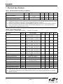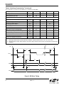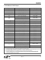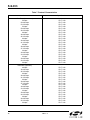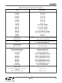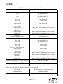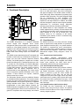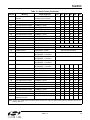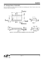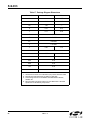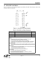
1
Si2493 V. 92 I SO MODEM ® WITH G L O B A L DAA Features This data sheet applies to Si2493 Revision D Data modem formats Over 6000 V capacitive isolation Parallel phone detect Globally-compliant line interface Overcurrent detection ITU-T, Bell bps up to 56 kbps V.21,V.22, V.29 Fast Connect V.44, V.42, V.42bis, MNP2-5 Automatic rate negotiation V.92 PCM upstream V.92 Quick connect V.92 Modem on hold 300 Type I and II caller ID decode No external ROM or RAM required UART, SPI, or parallel interface Flexible clock options Low-cost 32.768 kHz oscillator MHz oscillator 27 MHz clock input 4.915 Integrated DAA AT command set support SMS / MMS support Firmware upgradeable EEPROM interface Lead-free, RoHS-compliant packages Commercial or industrial temperature range DTMF detection/generation Ordering Information This data sheet is valid only for those chipset combinations listed on page 51. Pin Assignments Si2493 (16-Pin Option) Applications Set-top boxes Point-of-sale terminals Text / video telephones Digital video recorder Digital televisions Remote monitoring Description The Si2493 ISOmodem is a complete, ITU V.92-compliant, full-featured modem that provides conventional data formats with connect rates of up to 56,000 bps, full-duplex, over the Public Switched Telephone Network (PSTN). Offered as a chipset with the Si2493 system-side device and the Si3018 line-side device, the ISOmodem utilizes Silicon Laboratories’ patented Direct Access Arrangement (DAA) technology to provide a programmable telephone line interface with an unparalleled level of integration. This compact solution eliminates the need for a separate DSP, modem controller, codec, transformer, relay, opto-isolators, clocking crystal, and 2–4 wire hybrid. Available with a system-side packaging option of either a 16-pin SOIC or a 24-pin TSSOP, the Si2493 is ideal for embedded modem applications due to its flexibility, small footprint, and minimal external component count. Host Interface UART SPI Parallel Rev. 1.3 12/10 1 16 SS/RTS XTALO RI VD 2 15 DCD 3 4 14 13 MISO/RXD MOSI/TXD SCLK/CTS RESET 5 6 7 12 11 ESC VA GND INT 10 9 C1A C2A Si2493 System Side Si3018 Line Side Global DAA BOM Telco Tip Ring 8 Si2493 (24-Pin Option) CLKIN/XTALI 1 24 SDO/EECLK/D5 XTALO CLKOUT/EECS/A0 2 3 23 22 DCD/D4 ESC/D3 FSYNC/D6 4 21 VD3.3 GND 5 6 20 19 VD3.3 GND VDB VDA 7 18 SDI/EESD/D2 SS/RTS/D7 8 RI/D1 INT/DO AOUT/INT MOSI/TXD/WR 9 10 17 16 15 SCLK/CTS/CS 11 14 C1A RESET 12 13 C2A MISO/RXD/RD Si3018 QE DCT System Block Diagram Host CPU CLKIN/XTALI 1 RX IB 2 3 4 C1B C2B VREG 5 6 7 RNG1 8 16 15 DCT2 14 13 DCT3 QB QE2 12 11 10 9 IGND SC VREG2 RNG2 Capacitive Isolation Barrier Copyright © 2010 by Silicon Laboratories Si2493 Si2493 2 Rev. 1.3 Si2493 TABLE O F C ONTENTS Section Page 1. Electrical Specifications . . . . . . . . . . . . . . . . . . . . . . . . . . . . . . . . . . . . . . . . . . . . . . . . . . . . . . 4 2. Typical Application Schematic . . . . . . . . . . . . . . . . . . . . . . . . . . . . . . . . . . . . . . . . . . . . . . . . 11 3. Bill of Materials: Si2493 Chipset . . . . . . . . . . . . . . . . . . . . . . . . . . . . . . . . . . . . . . . . . . . . . . 13 4. Functional Description . . . . . . . . . . . . . . . . . . . . . . . . . . . . . . . . . . . . . . . . . . . . . . . . . . . . . . 18 4.1. Host Interface . . . . . . . . . . . . . . . . . . . . . . . . . . . . . . . . . . . . . . . . . . . . . . . . . . . . . . . . . 18 4.2. Command Mode . . . . . . . . . . . . . . . . . . . . . . . . . . . . . . . . . . . . . . . . . . . . . . . . . . . . . . . 19 4.3. Data Mode . . . . . . . . . . . . . . . . . . . . . . . . . . . . . . . . . . . . . . . . . . . . . . . . . . . . . . . . . . . 19 4.4. Fast Connect . . . . . . . . . . . . . . . . . . . . . . . . . . . . . . . . . . . . . . . . . . . . . . . . . . . . . . . . . 19 4.5. V.80 Synchronous Access Mode . . . . . . . . . . . . . . . . . . . . . . . . . . . . . . . . . . . . . . . . . . 19 4.6. Clocking . . . . . . . . . . . . . . . . . . . . . . . . . . . . . . . . . . . . . . . . . . . . . . . . . . . . . . . . . . . . . 19 4.7. Low-Power Modes . . . . . . . . . . . . . . . . . . . . . . . . . . . . . . . . . . . . . . . . . . . . . . . . . . . . . 19 4.8. Data Compression . . . . . . . . . . . . . . . . . . . . . . . . . . . . . . . . . . . . . . . . . . . . . . . . . . . . . 19 4.9. Error Correction . . . . . . . . . . . . . . . . . . . . . . . . . . . . . . . . . . . . . . . . . . . . . . . . . . . . . . . 19 4.10. Wire Mode . . . . . . . . . . . . . . . . . . . . . . . . . . . . . . . . . . . . . . . . . . . . . . . . . . . . . . . . . . 19 4.11. V.92 PCM Upstream . . . . . . . . . . . . . . . . . . . . . . . . . . . . . . . . . . . . . . . . . . . . . . . . . . 20 4.12. V.92 Quick Connect . . . . . . . . . . . . . . . . . . . . . . . . . . . . . . . . . . . . . . . . . . . . . . . . . . . 20 4.13. V.92 Modem-on-Hold . . . . . . . . . . . . . . . . . . . . . . . . . . . . . . . . . . . . . . . . . . . . . . . . . . 20 4.14. Caller ID Operation . . . . . . . . . . . . . . . . . . . . . . . . . . . . . . . . . . . . . . . . . . . . . . . . . . . 20 4.15. Parallel Phone Detection . . . . . . . . . . . . . . . . . . . . . . . . . . . . . . . . . . . . . . . . . . . . . . . 20 4.16. Overcurrent Detection . . . . . . . . . . . . . . . . . . . . . . . . . . . . . . . . . . . . . . . . . . . . . . . . . 22 4.17. Global Operation . . . . . . . . . . . . . . . . . . . . . . . . . . . . . . . . . . . . . . . . . . . . . . . . . . . . . 22 4.18. Firmware Upgrades . . . . . . . . . . . . . . . . . . . . . . . . . . . . . . . . . . . . . . . . . . . . . . . . . . . 22 4.19. DTMF Detection / Generation . . . . . . . . . . . . . . . . . . . . . . . . . . . . . . . . . . . . . . . . . . . 22 4.20. SMS/MMS Support . . . . . . . . . . . . . . . . . . . . . . . . . . . . . . . . . . . . . . . . . . . . . . . . . . . 22 4.21. Codec Interface (24-Pin Version Only) . . . . . . . . . . . . . . . . . . . . . . . . . . . . . . . . . . . . 22 4.22. EEPROM Interface (24-Pin Version Only) . . . . . . . . . . . . . . . . . . . . . . . . . . . . . . . . . . 22 4.23. AT Commands . . . . . . . . . . . . . . . . . . . . . . . . . . . . . . . . . . . . . . . . . . . . . . . . . . . . . . . 22 4.24. Extended AT Commands . . . . . . . . . . . . . . . . . . . . . . . . . . . . . . . . . . . . . . . . . . . . . . . 32 5. S-Registers . . . . . . . . . . . . . . . . . . . . . . . . . . . . . . . . . . . . . . . . . . . . . . . . . . . . . . . . . . . . . . . . 42 6. User-Access Registers (U-Registers) . . . . . . . . . . . . . . . . . . . . . . . . . . . . . . . . . . . . . . . . . . 45 7. Pin Descriptions: Si2493 (16-Pin Option) . . . . . . . . . . . . . . . . . . . . . . . . . . . . . . . . . . . . . . . 46 8. Pin Descriptions: Si2493 (24-Pin Option) . . . . . . . . . . . . . . . . . . . . . . . . . . . . . . . . . . . . . . . 48 9. Pin Descriptions: Si3018 . . . . . . . . . . . . . . . . . . . . . . . . . . . . . . . . . . . . . . . . . . . . . . . . . . . . . 50 10. Ordering Guide . . . . . . . . . . . . . . . . . . . . . . . . . . . . . . . . . . . . . . . . . . . . . . . . . . . . . . . . . . . 51 11. Package Markings (Top Markings) . . . . . . . . . . . . . . . . . . . . . . . . . . . . . . . . . . . . . . . . . . . 52 11.1. Si2493-D-FT Top Marking . . . . . . . . . . . . . . . . . . . . . . . . . . . . . . . . . . . . . . . . . . . . . . 52 11.2. Si2493-D-FS Top Marking . . . . . . . . . . . . . . . . . . . . . . . . . . . . . . . . . . . . . . . . . . . . . . 52 11.3. Si3018-F-FS Top Marking . . . . . . . . . . . . . . . . . . . . . . . . . . . . . . . . . . . . . . . . . . . . . . 52 12. Package Outline: 24-Pin TSSOP . . . . . . . . . . . . . . . . . . . . . . . . . . . . . . . . . . . . . . . . . . . . . 53 13. 24-Pin TSSOP Land Pattern . . . . . . . . . . . . . . . . . . . . . . . . . . . . . . . . . . . . . . . . . . . . . . . . . 54 14. Package Outline: 16-Pin SOIC . . . . . . . . . . . . . . . . . . . . . . . . . . . . . . . . . . . . . . . . . . . . . . . 55 15. 16-Pin SOIC Land Pattern . . . . . . . . . . . . . . . . . . . . . . . . . . . . . . . . . . . . . . . . . . . . . . . . . . . 57 Document Change List . . . . . . . . . . . . . . . . . . . . . . . . . . . . . . . . . . . . . . . . . . . . . . . . . . . . . . . . 58 Contact Information . . . . . . . . . . . . . . . . . . . . . . . . . . . . . . . . . . . . . . . . . . . . . . . . . . . . . . . . . . 60 Rev. 1.3 3 Si2493 1. Electrical Specifications Table 1. Recommended Operating Conditions Symbol Test Condition Min2 Typ Max2 Unit Ambient Temperature TA F-grade G-grade 0 –40 25 25 70 85 °C Si2493 Supply Voltage, Digital3 VD 3.0 3.3 3.6 V Parameter1 Notes: 1. The Si2493 specifications are guaranteed when the typical application circuit (including component tolerance) and any Si2493 and any Si3018 are used. See "2. Typical Application Schematic" on page 11. 2. All minimum and maximum specifications are guaranteed and apply across the recommended operating conditions. Typical values apply at nominal supply voltages and an operating temperature of 25 °C unless otherwise stated. 3. The digital supply, VD, operates from 3.0 to 3.6 V. Table 2. Loop Characteristics (VD = 3.0 to 3.6 V, TA = 0 to 70 °C for F-grade, TA = –40 to 85 °C for G-grade) Parameter Symbol DC Termination Voltage VTR DC Termination Voltage VTR DC Termination Voltage VTR DC Termination Voltage VTR DC Termination Voltage VTR DC Termination Voltage VTR DC Termination Voltage VTR On-Hook Leakage Current Operating Loop Current Operating Loop Current DC Ring Current ILK ILP ILP Ring Detect Voltage2 Ring Detect Voltage2 Ring Frequency Ringer Equivalence Number VRD VRD FR REN Test Condition ILIM1 IL = 20 mA, =0 DCV = 00, MINI = 11, DCR = 0 IL = 120 mA, ILIM = 0 DCV = 00, MINI = 11, DCR = 0 IL = 20 mA, ILIM = 0 DCV = 11, MINI = 00, DCR = 0 IL = 120 mA, ILIM = 0 DCV = 11, MINI = 00, DCR = 0 IL = 20 mA, ILIM = 1 DCV = 11, MINI = 00, DCR = 0 IL = 60 mA, ILIM = 1 DCV = 11, MINI = 00, DCR = 0 IL = 50 mA, ILIM = 1 DCV = 11, MINI = 00, DCR = 0 VTR = –48 V MINI = 00, ILIM = 0 MINI = 00, ILIM = 1 DC current flowing through ring detection circuitry RT = 0 RT = 1 Min Typ Max Unit — — 6.0 V 9 — — V — — 7.5 V 9 — — V — — 7.5 V 40 — — V — — 40 V — 10 10 — — — — 1.5 5 120 60 3 µA mA mA µA 12 18 15 — 15 21 — — 18 25 68 0.2 VRMS VRMS Hz Notes: 1. ILIM = U67, bit 9; DCV = U67, bits 3:2; MINI = U67, bits 13:12; DCR = U67, bit 7; RT = U67, bit 0. 2. The ring signal is guaranteed to not be detected below the minimum. The ring signal is guaranteed to be detected above the maximum. 4 Rev. 1.3 Si2493 TIP + 600 Si3018 IL VTR 10 µF – RING Figure 1. Test Circuit for Loop Characteristics Table 3. DC Characteristics, VD = 3.0 to 3.6 V (VD = 3.0 to 3.6 V, TA = 0 to 70 °C for F-grade, TA = –40 to 85 °C for G-grade) Parameter Symbol Test Condition Min Typ Max Unit High Level Input Voltage VIH 2.0 — — V Low Level Input Voltage VIL — — 0.8 V High Level Output Voltage VOH IO = –2 mA 2.4 — — V Low Level Output Voltage VOL IO = 2 mA — — 0.35 V Input Leakage Current IL –10 — 10 µA Pullup Resistance Pins RPU 50 125 200 k ID — 17 35 mA ID — 4.4 — mA — 80 — µA Total Supply Current* Total Supply Current, Wake-On-Ring* Total Supply Current, Powerdown * ID PDN = 1 *Note: All inputs at 0 or VD. All inputs held static except clock and all outputs unloaded (Static IOUT = 0 mA). Rev. 1.3 5 Si2493 Table 4. AC Characteristics (VD = 3.0 to 3.6 V, TA = 0 to 70 °C for F-grade, Fs = 8 kHz, TA = –40 to 85 °C for G-grade) Parameter Symbol Sample Rate Test Condition Fs Clock Input Frequency FXTL default Min Typ Max Unit — 8 — kHz — 4.9152 — MHz Mode1 — 27 — MHz Clock Input Frequency FXTL 27 MHz Clock Input Frequency FXTL 32 kHz Mode1 — 32.768 — kHz Receive Frequency Response Low –3 dBFS Corner, FILT = 0 — 5 — Hz Receive Frequency Response Low –3 dBFS Corner, FILT = 1 — 200 — Hz VFS — 1.1 — VPEAK Receive Full Scale Level2,3 VFS — 1.1 — VPEAK Dynamic Range4 DR ILIM = 0, DCV = 11, MINI = 00 DCR = 0, IL = 100 mA — 80 — dB Dynamic Range4 DR ILIM = 0, DCV = 00, MINI = 11 DCR = 0, IL = 20 mA — 80 — dB Dynamic Range4 DR ILIM = 1, DCV = 11, MINI = 00 DCR = 0, IL = 50 mA — 80 — dB Transmit Total Harmonic Distortion5 THD ILIM = 0, DCV = 11, MINI = 00 DCR = 0, IL = 100 mA — –72 — dB Transmit Total Harmonic Distortion5 THD ILIM = 0, DCV = 00, MINI = 11 DCR = 0, IL = 20 mA — –78 — dB Receive Total Harmonic Distortion5 THD ILIM = 0, DCV = 00, MINI = 11 DCR = 0, IL = 20 mA — –78 — dB Receive Total Harmonic Distortion5 THD ILIM = 1,DCV = 11, MINI=00 DCR = 0, IL = 50 mA — –78 — dB DRCID VIN = 1 kHz, –13 dBm — 50 — dB Transmit Full Scale Level2 Dynamic Range (Caller ID Mode) Notes: 1. Refer to “AN93: ISOmodem® Chipset Family Designer's Guide” for configuring clock input reset strapping. 2. Measured at TIP and RING with 600 termination at 1 kHz, as shown in Figure 1 on page 5. 3. Receive full scale level produces –0.9 dBFS at DTX. 4. DR = 20 x log |Vin| + 20 x log (rms signal/rms noise). Applies to both transmit and receive paths. Vin = 1 kHz, –3 dBFS. 5. Vin = 1 kHz, –3 dBFS. THD = 20 x log (rms distortion/rms signal). 6 Rev. 1.3 Si2493 Table 5. Absolute Maximum Ratings Parameter Symbol Value Unit DC Supply Voltage VD 4.1 V Input Current, Si2493 Digital Input Pins IIN ±10 mA Digital Input Voltage VIND –0.3 to (VD + 0.3) V CLKIN/XTALI Input Voltage VXIND –0.3 to (VD + 0.3) V TA –10 to 100 °C TSTG –40 to 150 °C Operating Temperature Range Storage Temperature Range Note: Permanent device damage may occur if the above absolute maximum ratings are exceeded. Functional operation should be restricted to the conditions as specified in the operational sections of this data sheet. Exposure to absolute maximum rating conditions for extended periods may affect device reliability. Table 6. Switching Characteristics1 (VD = 3.0 to 3.6 V, TA = 0 to 70 °C for F-grade, TA = –40 to 85 °C for G-grade) Parameter Symbol Min Typ Max Unit 2.048 — 49.152 MHz tBD –1 — 1 % RESET to RESET tRS 5.02 — — ms RESET to 1st AT Command tAT 300 — — ms Address Setup tAS 15 — — ns Address Hold tAH 0 — — ns WR Low Pulse Width tWL 50 — — ns tWDSU 20 — — ns Write Cycle Time tWC 120 — — ns Chip Select Setup tCSS 10 — — ns Chip Select Hold tCSH 0 — — ns tRL 50 — — ns tRLDD — — 20 ns Data Hold tDH 10 — — ns RD High to Hi-Z Time tDZ — — 30 ns UART Timing Parameters CLKOUT Output Clock Frequency Baud Rate Accuracy Reset Timing Parameters Parallel Timing Parameters Write Data Setup Time RD Low Pulse Width RD Low to Data Driven Time Notes: 1. All timing is referenced to the 50% level of the waveform. Input test levels are VIH = VD – 0.4 V, VIL = 0.4 V. 2. With 32.768 kHz clocking, allow 500 to the reset low-to-high minimum pulse on power-up and wake-from-power-down conditions. Rev. 1.3 7 Si2493 Table 6. Switching Characteristics1 (Continued) (VD = 3.0 to 3.6 V, TA = 0 to 70 °C for F-grade, TA = –40 to 85 °C for G-grade) Parameter Symbol Min Typ Max Unit tRC 120 — — ns tWRC 120 — — ns Read Cycle Time Write to Read Cycle Time Serial Peripheral Interface (SPI) Timing Parameters SS Falling to First SCLK Edge tSE 41 — — ns Last SCLK Edge to SS Rising tSD 41 — — ns SS Rising to MISO High-Z tSDZ — — 93 ns SCLK High Time tCKH 102 — — ns SCLK Low Time tCKL 102 — — ns MOSI Valid to SCLK Sample Edge tSIS 41 — — ns SCLK Sample Edge to MOSI Change tSIH 41 — — ns SCLK Shift Edge to MISO Change tSOH — — 93 ns SCLK cycle time tSCK 224 — — ns tNSS_INACT 81 — — ns Inactive time between SS actives Notes: 1. All timing is referenced to the 50% level of the waveform. Input test levels are VIH = VD – 0.4 V, VIL = 0.4 V. 2. With 32.768 kHz clocking, allow 500 to the reset low-to-high minimum pulse on power-up and wake-from-power-down conditions. SS T T SE T CKL SD SCLK* T CKH T T SIS SIH MOSI T SEZ T T SOH SDZ MISO Figure 2. SPI Slave Timing 8 Rev. 1.3 Si2493 t CSS t CSH t AS t AH CS ADDRESS = 0 or 1 A0 t RC t RL RD t DZ t RLDD t DH D[7:0] VALID DATA VALID DATA t RLDD Figure 3. Parallel Interface Read Timing t CSS t CSH t AS t AH CS A0 ADDRESS = 0 or 1 tW L tW C WR t W DSU t DH D[7:0] VALID DATA VALID DATA Figure 4. Parallel Interface Write Timing Rev. 1.3 9 Si2493 CS A0 ADDRESS = 0 or 1 WR tWRC RD tWDSU tDH D[7:0] VALID DATA VALID DATA tRLDD Figure 5. Parallel Interface Write Followed by Read Timing 10 Rev. 1.3 RESET_ RXD TXD CTS_ 8 5 6 7 16 15 14 11 3 RESET RXD TXD CTS RTS DCD ESC INT GPIO C51 C2A C1A XTALO CLKIN/XTALI GND 12 RTS_ DCD_ ESC INT_ GPIO 4 VD VA 13 9 10 2 1 C41 C40 Rev. 1.3 R9 C5 C2 C1 C6 10 7 4 6 5 VREG2 VREG IB C2B C1B U2 RNG1 RNG2 QE QE2 QB DCT2 DCT3 DCT RX 8 9 1 12 13 16 14 2 3 C4 R1 Q5 R2 R11 R10 C7 Q4 R4 R7 R8 R5 Q1 Z1 R3 Q2 Q3 C10 R6 + D1 C3 - FB1 FB2 C9 C8 R15 R16 Emissions option TIP RV1 RING Refer to AN93 Appendix A for layout guidelines. Please submit layout to Silicon Labs for review prior to PCB fabrication. Figure 6. Typical Si2493 Schematic with 16-pin System-Side Option R13 R12 Y1 External crystal option 1 2 U1 IGND C50 SC 15 + 11 VDD Si2493 2. Typical Application Schematic 11 RESET_ RTS_/D7 RXD/RD_ TXD/WR_ CTS_/CS_ CLKOUT/EECS_/A0 INT_/D0 RI_/D1 EESD/D2 EECLK/D5 DCD_/D4 ESC/D3 AOUT/INT_ D6 12 8 9 10 11 3 16 17 18 24 23 22 15 4 5 21 RESET RTS/D7 RXD/RD TXD/WR CTS/CS C51 C53 C2A C1A XTALO CLKIN/XTALI CLKOUT/EECS/A0 INT/D0 RI/D1 EESD/D2 EECLK/D5 DCD/D4 ESC/D3 AOUT/INT D6 U1 13 14 2 1 C41 C40 Rev. 1.3 R9 C5 Bias C2 C1 Bypass C6 10 7 4 6 5 VREG2 VREG IB C2B C1B U2 RNG1 RNG2 QE QE2 QB DCT2 DCT3 DCT RX 8 9 1 12 13 16 14 2 3 C4 R1 Q5 R10 Ring Detect/CID R2 R11 DC Term C7 Q4 R4 R7 R8 R5 Q1 Z1 R3 Q2 Q3 C10 Hookswitch R6 No Ground Plane In DAA Section + D1 C3 - Figure 7. Typical Si2493 Schematic with 24-pin System-Side Option R13 R12 Y1 External crystal option 1 2 VD3.3 VD 3.3 GND GND VDA VDB 6 20 7 19 C52 IGND 15 C50 SC 12 + 11 VDD FB1 FB2 C9 C8 R15 R16 Emissions option TIP RV1 RING Refer to AN93 Appendix A for layout guidelines. Please submit layout to Silicon Labs for review prior to PCB fabrication. Si2493 Si2493 3. Bill of Materials: Si2493 Chipset Component Value Supplier(s) C1, C2 33 pF, Y2, X7R, ±20% Panasonic, Murata, Vishay C3 10 nF, 250 V, X7R, ±20% Venkel, SMEC 1.0 µF, 50 V, Elec/Tant, ±20% Panasonic C4 C5, C6, C50, C52 1 0.1 µF, 16 V, X7R, ±20% Venkel, SMEC C7 2.7 nF, 50 V, X7R, ±20% Venkel, SMEC C8, C9 680 pF, Y2, X7R, ±10% Panasonic, Murata, Vishay C10 0.01 µF, 16 V, X7R, ±20% Venkel, SMEC C40 C41 4.9152 MHz: 33 pF, 16 V, NPO, ±5% 32.768 kHz: 18 pF, 16 V, NPO, ±5% 27 MHz: Not Populated 1 C51, C53 D1, D2 Venkel, SMEC 2 0.22 µF, 16 V, X7R, ±20% Venkel, SMEC Dual Diode, 225 mA, 300 V, CMPD2004S Central Semiconductor FB1, FB2 Ferrite Bead, BLM21AG601SN1 Murata Q1, Q3 NPN, 300 V, MMBTA42 OnSemi, Fairchild Q2 PNP, 300 V, MMBTA92 OnSemi, Fairchild Q4, Q5 NPN, 80 V, 330 mW, MMBTA06 OnSemi, Fairchild RV1 Sidactor, 275 V, 100 A Teccor, Protek, ST Micro R1 1.07 k, 1/2 W, 1% Venkel, SMEC, Panasonic R2 150 , 1/16 W, 5% Venkel, SMEC, Panasonic R3 3.65 k, 1/2 W, 1% Venkel, SMEC, Panasonic R4 2.49 k, 1/2 W, 1% Venkel, SMEC, Panasonic R5, R6 100 k, 1/16 W, 5% Venkel, SMEC, Panasonic R7, R8 20 M, 1/16 W, 5% Venkel, SMEC, Panasonic R9 1 M, 1/16 W, 1% Venkel, SMEC, Panasonic R10 536 , 1/4 W, 1% Venkel, SMEC, Panasonic R11 73.2 , 1/2 W, 1% Venkel, SMEC, Panasonic 56 , 1/16 W, 1% Venkel, SMEC, Panasonic R15, R16 0 , 1/16 W Venkel, SMEC, Panasonic U1 Si2493 Silicon Labs U2 Si3018 Silicon Labs R12, R13 3 32.768 kHz, 12 pF, 100 ppm, 35 k max ESR 4 Y1 4.9152 MHz, 20 pF, 100 ppm, 150 ESR ECS Inc., Siward 27 MHz (from external clock) Z1 Zener Diode, 43 V, 1/2 W, BZT84C43 On Semi Notes: 1. C52 and C53 should not be populated with the Si2493 16-pin package option. 2. Several diode bridge configurations are acceptable. For example, a single DF04S or four 1N4004 diodes may be used. 3. Murata BLM21AG601SN1 may be substituted for R15–R16 (0 ) to decrease emissions. 4. To ensure compliance with ITU specifications, frequency tolerance must be less than 100 ppm including initial accuracy, 5-year aging, 0 to 70 °C, and capacitive loading. For optimal V.92 PCM upstream performance, the recommended crystal accuracy is ±25 ppm. Rev. 1.3 13 Si2493 Table 7. Protocol Characteristics 14 Item Specification Data Rate (downstream) 56 kbps 54.666 kbps 53.333 kbps 52 kbps 50.666 kbps 49.333 kbps 48 kbps 46.666 kbps 45.333 kbps 44 kbps 42.666 kbps 41.333 kbps 40 kbps 38.666 kbps 37.333 kbps 36 kbps 34.666 kbps 33.333 kbps 32 kbps 30.666 kbps 29.333 kbps 28 kbps ITU-T V.90 ITU-T V.90 ITU-T V.90 ITU-T V.90 ITU-T V.90 ITU-T V.90 ITU-T V.90 ITU-T V.90 ITU-T V.90 ITU-T V.90 ITU-T V.90 ITU-T V.90 ITU-T V.90 ITU-T V.90 ITU-T V.90 ITU-T V.90 ITU-T V.90 ITU-T V.90 ITU-T V.90 ITU-T V.90 ITU-T V.90 ITU-T V.90 Data Rate (upstream) 48 kbps 46.666 kbps 45.333 kbps 44 kbps 42.666 kbps 41.333 kbps 40 kbps 38.666 kbps 37.333 kbps 36 kbps 34.666 kbps 33.333 kbps 32 kbps 30.666 kbps 29.333 kbps 28 kbps 26.666 kbps 25.333 kbps 24 kbps ITU-T V.92 ITU-T V.92 ITU-T V.92 ITU-T V.92 ITU-T V.92 ITU-T V.92 ITU-T V.92 ITU-T V.92 ITU-T V.92 ITU-T V.92 ITU-T V.92 ITU-T V.92 ITU-T V.92 ITU-T V.92 ITU-T V.92 ITU-T V.92 ITU-T V.92 ITU-T V.92 ITU-T V.92 Rev. 1.3 Si2493 Table 7. Protocol Characteristics (Continued) Item Specification Data Rate 33.6 kbps 31.2 kbps 28.8 kbps 26.4 kbps 24.0 kbps 21.6 kbps 19.2 kbps 16.8 kbps 14.4 kbps 12.0 kbps 9600 bps 7200 bps 4800 bps 2400 bps 1200 bps 300 bps 300 bps ITU-T V.34 ITU-T V.34 ITU-T V.34 ITU-T V.34 ITU-T V.34 ITU-T V.34 ITU-T V.34 ITU-T V.34 ITU-T V.34 or V.32bis ITU-T V.34 or V.32bis ITU-T V.34 or V.32bis ITU-T V.34 or V.32bis ITU-T V.34 or V.32bis ITU-T V.34, IV.32 bis, or V.22bis ITU-T V.22bis, V.23, or Bell 212A ITU-T V.21 Bell 103 Data Format Bit asynchronous Selectable 8, 9, 10, or 11 bits per character, which includes the start, stop, and parity bits. Compatibility ITU-T V.92, V.90, V.34, V.32bis, V.32, V.23, V.22bis, V.22, V.21, Bell 212A, and Bell 103 Operating Mode Switched network Two-wire full duplex Data Modulation 28 to 56 kbps (downstream) 24 to 48 kbps (upstream) 2.4 to 33.6 kbps 14.4 kbps 12.0 kbps 9600 kbps 9600 kbps 7200 kbps 4800 kbps 2400 kbps 1200 kbps 0 to 300 kbps V.90 as specified by ITU-T V.92 as specified by ITU-T V.34 as specified by ITU-T 128-level TCM/2400 Baud ±0.01% 64-level TCM/2400 Baud ±0.01% 32-level TCM/2400 Baud ±0.01% 16-level QAM/2400 Baud ±0.01% 16-level TCM/2400 Baud ±0.01% 4-level QAM/2400 Baud ±0.01% 16-level QAM/600 Baud ±0.01% 4-level PSK/600 Baud ±0.01% FSK 0–300 Baud ±0.01% Answer Tone ITU-T V.32bis, V.32, V.22bis, V.22, and V.21 modes Bell 212A and 103 modes 2100 Hz ±3 Hz 2225 Hz ±3 Hz Rev. 1.3 15 Si2493 Table 7. Protocol Characteristics (Continued) Item Transmit Carrier V.92 V.90 V.34 ITU-T V.32bis ITU-T V.32 ITU-T V.29 ITU-T V.22, V.22bis/Bell 212A Originate mode Answer mode ITU-T V.21 Originate mode Answer mode Bell 103 Originate mode Answer mode Specification As specified by ITU-T As specified by ITU-T As specified by ITU-T 1800 Hz ±0.01% 1800 Hz ±0.01% 1700 Hz ±1 Hz 1200 Hz ±0.5 Hz 2400 Hz ±1 Hz Mark (980 Hz ±12 Hz) Space (1180 Hz ±12 Hz) Mark (1650 Hz ±12 Hz) Space (1850 Hz ±12 Hz) Mark (1070 Hz ±12 Hz) Space (1270 Hz ±12 Hz) Mark (2025 Hz ±12 Hz) Space (2225 Hz ±12 Hz) Output Level Permissive—Switched network Receive Carrier ITU-T V.90 ITU-T V.34 ITU-T V.32bis ITU-T V.32 ITU-T V.29 ITU-T V.22, V.22bis/Bell 212A Originate mode Answer mode ITU-T V.21 Originate mode Answer mode Bell 103 Originate mode Answer mode –9 dBm maximum As specified by ITU-T As specified by ITU-T 1800 Hz ±7 Hz 1800 Hz ±7 Hz 1800 Hz ±7 Hz 2400 Hz ±7 Hz 1200 Hz ±7 Hz Mark (1650 Hz ±12 Hz) Space (1850 Hz ±12 Hz) Mark (1650 Hz ±12 Hz) Space (1850 Hz ±12 Hz) Mark (2025 Hz ±12 Hz) Space (2225 Hz ±12 Hz) Mark (1070 Hz ±12 Hz) Space (1270 Hz ±12 Hz) Carrier Detect (level for ITU-T V.22bis, V.22, V.21, 212, 103) in Switched Network Acquisition (–43 dBm) Release (–48 dBm) Hysteresis 2 dBm minimum ITU-T V.90, V.34, V.32/V.32bis are echo canceling protocols that use signal quality as criteria for maintaining connection. They also provide for self-training detection to force disconnect. 16 DTE Interface EIA/TIA-232-E (ITU-T V.24/V.28/ISO 2110) Line Equalization Automatic Adaptive Connection Options Loss of Carrier in ITU-T V.22bis and lower Rev. 1.3 Si2493 Table 7. Protocol Characteristics (Continued) Item Specification Phone Types 500 (rotary dial), 2500 (DTMF dial) Dialing Pulse and Tone DTMF Output Level Per Part 68 Pulse Dial Ratio Make/Break: 39/61% Ring Cadence On 2 seconds; Off 4 seconds Call Progress Monitor BUSY CONNECT (rate) NO ANSWER NO CARRIER NO DIALTONE OK RING RINGING Rev. 1.3 17 Si2493 4. Functional Description XTI UART Interface Data Bus C1 DAA Interface C2 Si3018/10 EEPROM Interface DSP EESD EECLK EECS RXD TXD CTS RTS DCD ESC RI XTO PLL Clocking Controller CLKOUT To Phone Line AOUT CS WR RD A0 D0-D7 Parallel Interface MISO MOSI SCLK SS SPI Interface The Si2493 allows for rapid integration into existing modem applications by providing a serial interface that can directly communicate to either a microcontroller via a UART interface or a PC via an RS-232 port. This interface allows for PC evaluation of the modem immediately upon powerup via the AT commands using standard terminal software. ROM Program Bus This device is ideal for embedded modem applications due to its small board space, low power consumption, and global compliance. The Si2493 solution includes a silicon DAA using Silicon Laboratories’ proprietary thirdgeneration DAA technology. This highly-integrated DAA can be programmed to meet worldwide PTT specifications for ac termination, dc termination, ringer impedance, and ringer threshold. In addition, the Si2493 has been designed to meet the most stringent worldwide requirements for out-of-band energy, billing-tone immunity, surge immunity, and safety requirements. RAM INT RESET 4.1. Host Interface Figure 8. Functional Block Diagram ® The Si2493 ISOmodem is a complete embedded modem chipset with integrated direct access arrangement (DAA) that provides a programmable line interface to meet global telephone line requirements. Available in two small packages, this solution includes a DSP data pump, modem controller, on-chip RAM and ROM, codec, DAA, analog output, and 27 MHz clock input. The Si2493 interfaces to the host processor through either an asynchronous serial interface, a synchronous Serial Peripheral Interface (SPI), or a parallel interface. The default is asynchronous serial communication. Selection of either SPI or parallel interface is done on power-up with reset strapping. Please refer to “AN93: ISOmodem® Chipset Family Designer's Guide” for details. The Si2493 accepts standard modem AT commands and provides connect rates up to 56/33.6/14.4/2.4 kbps fullduplex over the Public Switched Telephone Network (PSTN). The Si2493 features a complete set of modem protocols including all ITU-T standard formats up to V.92. 4.1.1. Asynchronous Serial Interface To provide the most flexibility, the Si2493 ISOmodem system-side device is offered in either a 24-pin TSSOP or a 16-pin SOIC package. The 16-pin version is footprintcompatible with the Si2401 ISOmodem and is recommended for most applications. The 16-pin version does not support the parallel, EEPROM or voice codec interface. If these features are required, customers should use the 24-pin version. The ISOmodem provides numerous additional features for embedded modem applications. The modem includes full type I and type II caller ID detection and decoding for global standards. Call progress monitoring is supported through standard result codes. The modem is also programmable to meet global settings. Because the Si2493 ISOmodem integrates the DAA, analog features, such as parallel phone detect, overcurrent detection, and global PTT compliance with a single design, are included. 18 The Si2493 supports asynchronous serial communication with data terminal equipment (DTE) at rates up to 307.2 kbps with the standard serial UART format. Upon powerup, the UART baud rate is automatically detected using the autobaud feature. 4.1.2. Serial Peripheral Interface (SPI) The serial peripheral interface (SPI) provides a flexible, full-duplex synchronous serial bus for host processor and Si2493 ISOmodem communication. When the Si2493 is powered up with SPI mode enabled the modem becomes an SPI slave, and the pins are configured to SS (slave select input, active low), MOSI (serial data input to modem), MISO (serial data output from modem) and SCLK (serial data clock input). Each SPI operation consists of a control-and-address byte and a data byte. 4.1.3. Parallel Interface (24-Pin Version Only) The Si2493 can also communicate via a parallel interface when using the 24-pin version. The parallel interface is an 8-bit data bus with a single bit address to memory mapped registers. Rev. 1.3 Si2493 4.2. Command Mode 4.7. Low-Power Modes Upon reset, the ISOmodem® is in command mode and accepts “AT” commands. An outgoing modem call can be made using the “ATDT#” (tone dial) or “ATDP#” (pulse dial) command after the device is configured. If the handshake is successful, the modem responds with the response codes detailed in Table 12 on page 40 and enters data mode. The Si2493 provides multiple low power modes. Using the S24 S-register, the Si2493 can be set to automatically enter sleep mode after a pre-programmed time of inactivity with either the DTE or the remote modem. The sleep mode is entered after (S24) seconds have passed since the last DTE activity, after the transmit FIFO is empty, and after the last data are received from the remote modem. 4.3. Data Mode The Si2493 ISOmodem is in data mode while it has a telephone line connection to another modem or is in the process of establishing a connection. Data protocols are available to provide error correction to improve reliability (V.42 and MNP2-4) and data compression to increase throughput (V.44, V.42bis and MNP5). Each connection between two modems in data mode begins with a handshaking sequence. During this sequence, the modems determine the line speed, data protocol, and related parameters for the data link. Configuration through AT commands determines the range of choices available to the modem during the negotiation process. 4.4. Fast Connect The Si2493 supports a fast connect mode of operation to reduce the time of a connect sequence in originate mode. The Fast Connect modes can be enabled for V.21, V.22, Bell103, and V.29 modulations. See AN93 for details. 4.5. V.80 Synchronous Access Mode The Si2493 supports a V.80 synchronous access mode of operation, which operates with an asynchronous DTE and a synchronous DCE. See “AN93: ISOmodem® Chipset Family Designer's Guide”. 4.6. Clocking The Si2493 contains an on-chip phase-locked loop (PLL) and clock generator to derive all necessary internal system clocks from a single clock input. A 32.768 kHz or 4.9152 MHz crystal can be used across XTALI and XTALO pins to form the master clock (±100 ppm max, ±25 ppm recommended) for the ISOmodem. The 32.768 kHz option can provide lower BOM costs and smaller footprint. Alternatively, a clock input of 27 MHz, 4.9152 MHz, or 32.768 kHz can be provided to XTALI if that clock source is available in the system. A 4.9152 MHz clock input is the default clock option. Other clock options are selected at power-up through reset strapping. Refer to AN93 for details. Additionally, the Si2493 can be placed in wake-on-ringmode using the command, AT&Z. In either mode, the ISOmodem remains in the sleep state until one of the following occurs: A 1-to-0 transition on TXD (UART mode). A 1-to-0 transition on SS (SPI mode). A 1-to-0 transition on CS (parallel mode). An incoming ring is detected. A parallel telephone is picked up. Line polarity reversal The Si2493 may also be placed in a complete powerdown mode. Once the Si2493 completely powers down, it can only be powered back on via the RESET pin. 4.8. Data Compression The modem can achieve DTE (host-to-ISOmodem) speeds greater than the maximum DCE (modem-tomodem) speed through the use of a data compression protocol. The compression protocols available are the ITU-T V.44, V.42bis, and MNP5 protocols. Data compression attempts to increase throughput by compressing the data before actually sending it. Thus, the modem is able to transmit more data in a given period of time. 4.9. Error Correction The Si2493 ISOmodem can employ error correction (reliable) protocols to ensure error-free delivery of asynchronous data sent between the host and the remote end. The Si2493 supports V.42 and MNP2-4 error correction protocols. V.42 (LAPM) is most commonly used and is enabled by default. 4.10. Wire Mode Wire mode is used to communicate with standard nonerror correcting modems. When optioned with \N3, the Si2493 falls back to wire mode if it fails in an attempt to negotiate a V.42 link with the remote modem. Error correction and data compression are not active in wire mode. Rev. 1.3 19 Si2493 4.11. V.92 PCM Upstream 4.14. Caller ID Operation The Si2493 supports the ITU-V.92 PCM upstream data protocol. This protocol allows the ISOmodem to connect at speed up to 48 kbps upstream. Previously the upstream connection rate was limited to 33.6 kbps. The PCM upstream mode is enabled by default; to disable, issue the AT command +PIG = 1 (see Table 8 on page 23). To view both downstream and upstream connect speeds in the connect result message, issue the command “AT \V4” or “AT+MR”. The Si2493 supports full type I and type II caller ID detection and decode. Caller ID is supported for the US Bellcore, European ETSI, UK, and Japanese protocols and is enabled via the +VCID, +VCDT, and +PCW commands. 4.12. V.92 Quick Connect The Si2493 supports the ITU-V.92 quick connect protocol. Quick connect enables the modem to save and reuse line condition parameters to reduce startup negotiation time. The quick connect feature is enabled by default in the Si2493. For information on changing the quick connect settings, see the +PSS and +PQC commands shown in Table 8 on page 23. 4.13. V.92 Modem-on-Hold The modem-on-hold (MOH) feature allows the modem user to answer an incoming call while connected online without dropping the internet connection. The modem will remain “on hold” for a period of time determined by the host and the ISP. There are four AT commands that control the operation of MOH. The commands are as follows: +PCW, +PMH, +PMHT, +PMHR. By changing these parameters, the user can enable/disable call waiting and MOH, set the MOH request timeout, and set the MOH initiate timeout. For further details and syntax on these commands see Table 8 on page 23. The MOH feature is most useful when the Si2493 is connected to a central office that allows call waiting. 20 4.15. Parallel Phone Detection The ISOmodem® is able to detect when another telephone, modem, or other device is using the phone line. This allows the host to avoid interrupting another phone call when the phone line is already in use and to intelligently handle an interruption when the ISOmodem is using the phone line. 4.15.1. On-Hook Line-in-use Detection When the ISOmodem is sharing the telephone line with other devices, it is important that it not interrupt a call in progress. To detect whether another device is using the shared telephone line, the host can use the ISOmodem to monitor the TIP-RING dc voltage with the line voltage sense (LVS) register (U6C, bits 15:8). The LVS bits have a resolution of 1 V per bit with an accuracy of approximately ±10%. Bits 0 through 6 of this 8-bit signed twos complement number indicate the value of the line voltage, and the sign bit (bit 7) indicates the polarity of TIP and RING. The ISOmodem can also monitor the TIP-RING dc voltage using the LVCS register (U79, bits 4:0). See Figure 9 on page 21. See also the %Vn commands for automatic line-in-use detection. 4.15.2. Off-Hook Intrusion Detection When the ISOmodem is off-hook, an algorithm is implemented in the ISOmodem to automatically monitor the TIP-RING loop current via the LVCS register. During the off-hook state, the LVCS register switches from representing the TIP-RING voltage to representing the TIP-RING current. See Figure 10 on page 21. Upon detecting an intrusion, the ISOmodem alerts the host of the condition via the INT pin. Rev. 1.3 Si2493 30 25 20 LVC S BITS 15 10 5 0 0 3 6 9 12 15 18 21 24 28 30 33 36 39 42 45 47 51 54 57 60 63 66 69 72 75 78 81 84 87 100 Loop Voltage (V) Figure 9. Loop Voltage Overload 30 25 20 CTR21 only LVCS BITS 15 10 5 0 0 3 6 9 12 15 18 21 24 27 30 33 36 39 42 45 48 51 54 57 60 63 66 69 72 75 78 81 84 87 90 93 140 Loop Current (mA) Figure 10. Loop Current Rev. 1.3 21 Si2493 4.16. Overcurrent Detection 4.20. SMS/MMS Support The Si2493 includes an overcurrent detection feature that measures the loop current at a programmable time after the Si2493 goes off-hook. This allows the Si2493 to detect if it is connected to an improper telephone line. The overcurrent detection feature may be enabled by setting the OCDM bit (U70, bit 11). OHT (U77, bits 8:0) sets the delay after off-hook until the loop current is measured. See “AN93: ISOmodem® Chipset Family Designer's Guide” for details. Short Message Service (SMS) is a service that allows text messages to be sent and received from one telephone to another via an SMS service center. Multimedia Messaging Service (MMS) extends the core SMS capability to send messages that include multimedia content. The Fax ISOmodem provides an interface that offers a great deal of flexibility in handling multiple SMS standards. This flexibility is possible because most of the differences between standards are handled by the host using the raw data itself. The Si2493 performs the necessary modulation/ demodulation of the data and provides two options for message packet structure (Protocol 1 and Protocol 2, as defined in ETSI ES 201 912). The rest of the data link layer and transfer layer are defined by the host system. The content of the message is entirely up to the host including any checksum or CRC. ETSI ES 201 912 describes two standard data and transfer layers that are commonly used. SMS typically relies on caller identification information to determine if the call should be answered using an SMS device or not. See “6.4. SMS Support” in AN93 for more information on how to configure the modem for SMS support. 4.17. Global Operation The Si2493 chipset contains an integrated silicon direct access arrangement (Silicon DAA) that provides a programmable line interface to meet international telephone line interface requirements. “AN93: Modem Designer’s Guide” gives the DAA register settings required to meet international PTT standards. Additionally, the user-access registers (via the AT:U and AT:R commands) may be programmed for countryspecific settings, such as dial tone, ring, ringback, and busy tone. See AN93 for complete details. 4.18. Firmware Upgrades The Si2493 contains an on-chip program ROM that includes the firmware required for the features listed in this data sheet. In addition, the Si2493 contains on-chip program RAM to accommodate minor changes to the ROM firmware. This allows Silicon Labs to provide future firmware updates to optimize the characteristics of new modem designs and those already deployed in the field. See AN93 for complete details. 4.19. DTMF Detection / Generation The Si2493 provides comprehensive DTMF tone generation and detection. The ISOmodem can generate single tones or DTMF tones using the +VTS command. DTMF tones may also be generated during dialing using the “ATDT” command. DTMF detection is only available in voice mode (FCLASS = 8). DTMF digits are reported from the modem to the host using <DLE> shielding. 4.21. Codec Interface (24-Pin Version Only) In order to support a full range of voice and data applications, the Si2493 includes an optional serial interface that connects to an external voice codec (Si3000). See AN93 for complete details. 4.22. EEPROM Interface (24-Pin Version Only) The Si2493 supports an optional serial peripheral interface (SPI) bus serial EEPROM Mode 3 with a 16-bit (8–64 kbit range) address. Upon powerup, if a pulldown resistor 10 k is placed between D6 and GND, the ISOmodem attempts to detect an EEPROM. The EEPROM is intended first for setting custom defaults, second for automatically loading firmware upgrades, and third to allow for user-defined AT command macros for use in custom AT commands or country codes. See AN93 for complete details. 4.23. AT Commands At powerup, the Si2493 is in the AT command mode. In command mode, the modem monitors the input (serial or parallel) checking constantly for a valid command (AT commands are described in Table 8.) 22 Rev. 1.3 Si2493 Table 8. Basic AT Command Set (Command Defaults in Bold) Command Action $ Display AT command mode settings. A Answer incoming call A/ Dn Re-execute last command. This is the only command not preceded by “AT” or followed by a <CR>. Dial The dial command, followed by 1 or more dial command modifiers, manually dials a phone number: Modifier Function ! or & Flash hook switch for FHT (U4F) ms (default: 500 ms) Pause before continuing for S8 seconds (default: , or < 2 seconds) ; Return to AT command mode @ Wait for silence. Polarity reversal detect. By placing the “G” character in the dial string (i.e. ATDTG1), the Si2493 will monitor the telephone line for polarity reversals. If a busy tone is detected, the Si2493 will report “POLARITY REVERSAL” if a polarity reversal was detected or “NO POLARITY REVERSAL” if a polarity reversal was not detected. G In each case, the result code is followed by “OK”. If the S7 timeout occurs before a busy tone is detected, the Si2493 will report “NO CARRIER”. Polarity reversal monitoring begins after the last digit is dialed and ends when the busy tone is detected or S7 timeout occurs. Note: It is not possible to establish a modem connection when using this command. L P T W En Local DTE echo E0 Disable E1 Enable Hn Hook switch. H0 Go on-hook (hang up modem). Redial last number. Pulse (rotary) dialing—pulse digits: 0, 1, 2, 3, 4, 5, 6, 7, 8, 9 Tone (DTMF) dialing—DTMF digits: *, #, A, B, C, D, 0, 1, 2, 3, 4, 5, 6, 7, 8, 9. Wait for dial tone before continuing for S14 seconds (default: 12 seconds). Blind dialing modes X0, X1 and X3 do not affect the W command. If the DOP bit (U7A, bit 7) is set, the “ATDTW” command will cause the ISOmodem® to pause dialing and either report an “OK” if a dialtone is detected or “NO DIALTONE” if a dial tone is not detected. Rev. 1.3 23 Si2493 Table 8. Basic AT Command Set (Command Defaults in Bold) (Continued) Command H1 Go off-hook. In Identification and checksum. I0 I1 Display Si2493 revision code. B: Revision B C: Revision C, etc. Display Si2493 firmware revision code (numeric). I7 Display line-side revision code. 18C = Si3018 revision C Display the ISOmodem® model number. “2493” = Si2493 Diagnostic results 1. See “AN93: ISOModem® Chipset Family Designer’s Guide” for details. I8 Diagnostic results 2. See AN93 for details. Ln Speaker volume operation L1 Low speaker volume L2 Medium speaker volume L3 High speaker volume Mn Speaker operation (via AOUT). M0 Speaker is always off. M1 Speaker is on while dialing and handshaking; off in data mode. M2 Speaker is always on. M3 Speaker is off while dialing, on during handshaking and retraining. On Return to data mode from Command mode operation. O0 Return to data mode. O1 Return to data mode and perform a full retrain (at any speed except 300 bps). O2 Return to data mode and perform rate renegotiation. Qn Response mode. Q0 Enable result codes (see Table 12 on page 40) Q1 Disable result codes (enable quiet mode). I3 I6 24 Action R Initiate V.23 reversal. Sn S-register operation (see Table 13 on page 42). S$ List contents of all S registers. Sn? Display contents of S-register n. Sn=x Set S-register n to value x (where n and x are decimal values). Vn Result code type (see Table 12 on page 40). V0 Numeric result codes. Rev. 1.3 Si2493 Table 8. Basic AT Command Set (Command Defaults in Bold) (Continued) Command V1 Xn X0 X1 Action Verbal result codes Call Progress Monitor (CPM)—This command controls which CPM signals are monitored and reported to the host from the Si2493. (See Table 12 on page 40.) Basic results; disable CPM—Blind dial (does not wait for dial tone). CONNECT message does not include speed. Extended results; disable CPM—Blind dial. CONNECT message includes speed. X3 Extended results and detect dial tone only—Add dial tone detection to X1 mode. Does not blind dial. Extended results and detect busy only—Add busy tone detection to X1 mode. X4 Extended results, full CPM—Full CPM enabled, CONNECT message includes speed. X2 Y0 Extended results—Full CPM enabled including ringback detection. Adds ringback detection to X4 mode. Long space disconnect—Modem hangs up after 1.5 seconds or more of continuous space while on-line. Disable. Y1 Enable. X5 Yn Z :E :I :M :P :R :U Hard Reset—This command is functionally equivalent to pulsing the RESET pin low. (See tAT in Table 6 on page 7.) Read from serial EEPROM. Interrupt Read—This command causes the ISOmodem® to report the lower 8 bits of the interrupt register I/O Control 0 (U70). The CID, OCD, PPD, and RI bits also are cleared, and the INT pin (INT bit in parallel mode) is deactivated on this read. Write to serial EEPROM. Program RAM Write—This command is used to upload firmware supplied by Silicon Labs to the Si2493. The format for this command is AT:Paaaa,xxxx,yyyy,.... where aaaa is the first address in hexadecimal and xxxx,yyyy,.... is data in hexadecimal. Only one :P command is allowed per AT command line. No other commands can be concatenated in the :P command line. This command is only for use with special files provided by Silicon Laboratories. Do not attempt to use this command for any other purpose. User-Access Register Read—This command allows the user to read from the user-access registers (see "6. User-Access Registers (U-Registers)" on page 45). The format is “AT:Raa”, where: aa = user-access address in hexadecimal. The “AT:R” command causes all the U- registers to be displayed. User-Access Register Write—This command allows the user to write to the 16-bit useraccess registers. (See page page 45.) The format is “AT:Uaa,xxxx,yyyy,zzzz,...” where aa = user-access address in hexadecimal. xxxx = Data in hexadecimal to be written to location aa. yyyy = Data in hexadecimal to be written to location (aa + 1). zzzz = Data in hexadecimal to be written to location (aa + 2). etc. Rev. 1.3 25 Si2493 Table 8. Basic AT Command Set (Command Defaults in Bold) (Continued) Command +DR=X +DS Options +DS = A +DS = A,B +DS = A,B,C +DS = A,B,C,D Action Data compression reporting. Mode X 0 Disabled 1 Enabled If enabled, the intermediate result code is transmitted at the point after error control negotiation. The format of this result code is as follows: Result code Mode +DR:NONE Data compression is not in use +DR:V42B Rec. V.42bis is in use in both directions +DR:V42B RD Rec. V.42bis is in use in receive direction only +DR:V42B TD Rec. V.42bis is in use in transmit directions only Controls V.42bis data compression function. A Direction 0 No compression 1 Transmit only 2 Receive only 3 Both Directions B Compression_negotiation 0 Do not disconnect if V.42 is not negotiated. 1 Disconnect is V.42 is not negotiated. C Maximum dictionary size 512 D +DS44 Options +DS44 = A +DS44 = A,B +DS44 = A,B,C +ES Options +ES = A +ES = A,,C 26 Maximum string size 6 to 250 (28 default) Controls V.44 data compression function. A Direction 0 No compression 1 Transmit only 2 Receive only 3 Both Directions B Compression_negotiation 0 Do not disconnect if V.44 is not negotiated. 1 Disconnect if Rec. V.42 is not negotiated. C Capability 0 Stream method Enable synchronous access mode. A Specifies the mode of operation when initiating a modem connection. D Disable synchronous assess mode. 6 Enable synchronous access mode when connection is completed and data state is entered. B Specifies fallback mode of operation. This parameter should not be used. C Specifies the mode of operation when answer a modem connection. D Disable synchronous assess mode. 8 Enable synchronous access mode when connection is completed and data state is entered. Rev. 1.3 Si2493 Table 8. Basic AT Command Set (Command Defaults in Bold) (Continued) Command Action Synchronous access mode control options A Specifies action taken if an underrun condition occurs during transparent sub-mode. 0 Modem transmits 8-bit SYN sequences on idle. B Specifies action taken if an underrun condition occurs after a flag during framed submode 0 Modem transmits 8-bit HDLC flags on idle. C Specifies action taken if an underrun or overrun condition occurs after a non-flag during +ESA Options framed sub-mode. +ESA = A 0 Modem transmits abort on underrun in middle of frame. +ESA = A,B 1 Modem transmits flag on underrun in middle of frame and notifies host of underrun +ESA = A,B,C or overrun. +ESA = A,B,C,E Specifies V.34 half duplex operation. +ESA = A,B,C,E,F D This parameter should not be used. +ESA = A,B,C,E,F E Specifies CRC polynomial used while in framed sub-mode. ,G 0 CRC generation checking disable. 1 16-bit CRC generation and checking is performed by the modem. F Specifies NRZI encoding and decoding. 0 NRZI encoding and decoding disabled. G Specifies SYN. 255 Class 1 Mode Enable for V.29 fast connect. X Mode +FCLASS = X 0 Off 1 Enables support for Class 1 mode for use in the V.29 fast connect mode. Class 1 Receive Carrier for V.29 fast connect. X Mode 2 Transmit V.21 (980 Hz) tone for longer than 100 ms, then send answer tone +FRM = X (2100/2225 Hz) for 200 ms. 95 V.29 short synchronous. 96 V.29 full synchronous. Class 1 Transmit Carrier for V.29 fast connect. X Mode 2 Transmit V.21 (980 Hz) tone. 53 Same as &T4, but transmit V.29 7200 bps. Data pattern set by S40 register. AT + FCLASS = 0 must be sent to restore the ISOmodem® to normal operation after +FTM = X test. 54 Same as &T4, but transmit V.29 9600 bps. Data pattern set by S40 register. AT + FCLASS = 0 must be sent to restore the ISOmodem to normal operation after test. 95 V.29 short synchronous. 96 V.29 full synchronous. Rev. 1.3 27 Si2493 Table 8. Basic AT Command Set (Command Defaults in Bold) (Continued) Command +GCI = X Action Country settings - Automatically configure all registers for a particular country. X Country 0 Japan 9 Australia A Austria F Belgium 16 Brazil 1B Bulgaria 20 Canada 26 China 27 Columbia 2E Czech Republic 31 Denmark 35 Ecuador 3C Finland 3D France 42 Germany 46 Greece 50 Hong Kong 51 Hungary 53 India 57 Ireland 58 Israel 59 Italy 61 South Korea 69 Luxembourg 6C Malaysia 73 Mexico 7B Netherlands 7E New Zealand 82 Norway 87 Paraguay 89 Philippines 8A Poland 8B Portugal 9C Singapore 9F South Africa A0 Spain A5 Sweden A6 Switzerland B8 Russia B4 United Kingdom B5 United States FE Taiwan Note: U-registers are configured to Silicon Laboratories’ recommended values. The +GCI command resets the U-registers and the S7 and S6 S-registers to default values before setting countryspecific values. Changes may be made by writing individual registers after sending the AT+GCI command. Refer to “AN93: ISOModem® Chipset Family Designer’s Guide” for details. +GCI? +GCI = ? 28 List current country code setting (response is: + GCI:<setting>) List all possible country code settings. Rev. 1.3 Si2493 Table 8. Basic AT Command Set (Command Defaults in Bold) (Continued) Command Action Specifies the flow control to be implemented. A Specifies the flow control method used by the host to control data from the modem 0 None 1 Local XON/OFF flow control. Does not pass XON/XOFF character to the remote +IFC Options modem. +IFC = A 2 Hardware flow control (RTS) +IFC = A,B B Specifies the flow control method used by the modem to control data from the host 0 None 1 Local XON/OFF flow control. 2 Hardware flow control (CTS). Transmit flow control threshold. A Threshold above which the modem will generate a flow off signal +ITF Options <0 to 511> bytes +ITF = A B Threshold below which the modem will generate a flow on signal +ITF = A,B <0 to 511> bytes +ITF = A,B,C C Polling interval for <EM><BNUM> indicator 0 to 300 in 10 msec units. Modulation reporting control. X Mode 0 Disabled 1 Enabled +MR = X If enabled, the intermediate result code is transmitted at the point during connect negotiation. The format of this result code is as follows: +MCR: <carrier> e.g. +MCR: V32B +MRR: <rate> e.g. +MRR: 14400 Modulation Selection. A Preferred modem carrier V21 ITU-T V.21 V22 ITU-T V.22 V22B ITU-T V.22bis V32 ITU-T V.32 +MS Options V32B ITU-T V.32bis +MS = A V34 ITU-T V.34 +MS = A,B V90 ITU-T V.90 +MS = A,B,C V92 ITU-T V.92 +MS = A,B,C,D B Automatic modulation negotiation +MS = A,B,C,D,E 0 Disabled +MS = A,B,C,D,E, 1 Enabled F C,D Min TX rate/Max TX rate are optional numeric values that specify the lowest value at which the DCE may establish a connection. If unspecified (set to 0), they are determined by the carrier and automode settings. E,F Min RX rate/Max RX rate are optional numeric values which specify the highest value at which the DCE may establish a connection. If unspecified (set to 0), they are determined by the carrier and automode settings. Rev. 1.3 29 Si2493 Table 8. Basic AT Command Set (Command Defaults in Bold) (Continued) Command +PCW = X 30 Action Controls the action to be taken upon detection of call waiting. Mode X 0 Toggle RI and collect type II Caller ID if enabled by +VCID. 1 Hang up. 2 Ignore call waiting. +PIG=X Controls the use of PCM upstream in a V.92 DCE. Mode X 0 Enable PCM upstream. 1 Disable PCM upstream. +PMH=X Controls the modem-on-hold procedures. Mode X 0 Enables V.92 MOH. 1 Disables V.92 MOH. +PMHF=X V.92 MOH hook flash. This command causes the DCE to go on-hook and then return offhook. If this command is initiated and the modem is not On Hold, Error is returned. +PMHR=X Initiate MOH. Requests the DCE to initiate or to confirm a MOH procedure. Valid only if MOH is enabled. X Mode 0 V.92 MOH request denied or not available. 1 MOH with 10 s timeout granted. 2 MOH with 20 s timeout granted. 3 MOH with 30 s timeout granted. 4 MOH with 40 s timeout granted. 5 MOH with 1 min. timeout granted. 6 MOH with 2 min. timeout granted. 7 MOH with 3 min. timeout granted. 8 MOH with 4 min. timeout granted. 9 MOH with 6 min. timeout granted. 10 MOH with 8 min. timeout granted. 11 MOH with 12 min. timeout granted. 12 MOH with 16 min. timeout granted. 13 MOH with indefinite timeout granted. 14 MOH request denied. Future request will also be denied. Rev. 1.3 Si2493 Table 8. Basic AT Command Set (Command Defaults in Bold) (Continued) Command +PMHT=X +PQC=X +PSS=X +VCDT = X +VCID = X +VCIDR? Action Controls access to MOH request and sets the timeout value. X Mode 0 Deny V.92 MOH request. 1 Grant MOH with 10 s timeout. 2 Grant MOH with 20 s timeout. 3 Grant MOH with 30 s timeout. 4 Grant MOH with 40 s timeout. 5 Grant MOH with 1 min. timeout. 6 Grant MOH with 2 min. timeout. 7 Grant MOH with 3 min. timeout. 8 Grant MOH with 4 min. timeout. 9 Grant MOH with 6 min. timeout. 10 Grant MOH with 8 min. timeout. 11 Grant MOH with 12 min. timeout. 12 Grant MOH with 16 min. timeout. 13 Grant MOH with indefinite timeout. V.92 Phase 1 and Phase 2 Control. X Mode 0 Enable Short Phase 1 and Short Phase 2. 1 Enable Short Phase 1. 2 Enable Short Phase 2. 3 Disable Short Phase 1 and Short Phase 2. Selection of full or short startup procedures. X Mode 0 The DCEs decide to use short startup procedures. 1 Forces the use of short startup procedures on next and subsequent connections. 2 Forces the use of full startup procedures on next and subsequent connections. Caller ID Type. X Mode 0 After ring only 1 Always on (Recommended Setting) 2 UK 3 Japan Caller ID Enable. X Mode 0 Off 1 On—formatted 2 On—raw data format Type II caller ID information — The Si2493 will display “+VCDIR:” followed by raw caller ID information including checksum. Rev. 1.3 31 Si2493 4.24. Extended AT Commands The extended AT commands are supported by the Si2493 and are described in Tables 9 through 11. Table 9. Extended AT& Command Set (Command Defaults in Bold) Command &$ Display AT& current settings. &D0 ESC is not used &D1 ESC escapes to command mode from data mode if also enabled by HES U70, bit 15. &D2 ESC assertion during a modem connection causes the modem to go on-hook and return to command mode. &D3 ESC assertion causes ATZ command (reset and return OK result code). &F 32 Action Restore factory default settings. &Gn Line connection rate limit—This command sets an upper limit on the line speed that the Si2493 can connect. Note that the &Hn commands may limit the line speed as well (&Gn not used for &H0 or &H1). Not all modulations support rates given by &G. Any improper setting will be ignored. &G3 1200 bps max &G4 2400 bps max &G5 4.8 kbps max &G6 7.2 kbps max &G7 9.6 kbps max &G8 12 kbps max &G9 14.4 kbps max &G10 16.8 kbps max &G11 19.2 kbps max &G12 21.6 kbps max &G13 24 kbps max &G14 26.4 kbps max &G15 28.8 kbps max &G16 31.2 kbps max &G17 33.6 kbps max &Hn Switched network handshake mode—&Hn commands must be on a separate command line from ATD, ATA, or ATO commands. &H0 V.90 with automatic fallback (56 kbps to 300 bps) &H1 V.90 only (56 kbps to 28 kbps) Rev. 1.3 Si2493 Table 9. Extended AT& Command Set (Command Defaults in Bold) (Continued) Command Action &H2 V.34 with automatic fallback (33.6 kbps to 300 bps) &H3 V.34 only (33.6 kbps to 2400 bps) &H4 ITU-T V.32bis with automatic fallback (14.4 kbps to 300 bps) &H5 ITU-T V.32bis only (14.4 kbps to 4800 bps) &H6 ITU-T V.22bis only (2400 bps or 1200 bps) &H7 ITU-T V.22 only (1200 bps) &H8 Bell 212 only (1200 bps) &H9 Bell 103 only (300 bps) &H10 ITU-T V.21 only (300 bps) &H11 V.23 (1200/75 bps) &H12 V.92 with automatic fallback &Pn Japan pulse dialing &P0 Configure Si2493 for 10 pulse-per-second pulse dialing. For Japan. &P1 Configure Si2493 for 20 pulse-per-second pulse dialing. For Japan. &Tn Test mode &T0 Cancel test mode (Escape to command mode to issue AT&T0). This command will also report the number of bit errors encountered on the previous &T4 or &T5 test. &T2 Initiate ITU-T V.54 (ANALOOP) test. Modulation set by &H AT command. Test loop is through the DSP (Si2493 device) only. ISOmodem® echoes data from TX pin (Register 0 in parallel mode) back to RX pin (Register 0 in parallel mode). &T3 Initiate ITU-T V.54 (ANALOOP) test. Modulation set by &H AT command. Test loop is through the DSP (Si2493), DAA interface section (Si2493), DAA interface (Si3018), and analog hybrid circuit (Si3018). ISOmodem echoes data from TX pin (Register 0 in parallel mode) back to RX pin (Register 0 in parallel mode). Phone line termination required as in Figure 1. To test only the link operation, the hybrid and AFE codec can be removed from the test loop by setting the DL bit (U62, bit 1). &T4 Initiate transmit as originating modem with automatic data generation. Modulation, data rate, and symbol rate are set by &H, &G, and S41. Data pattern is set by the S40 register. Continues until the ATH command is sent after an escape into command mode. Data is also demodulated as in ANALOOP, and any bit errors are counted to be displayed after the test using &T0. &T5 Initiate transmit as answering modem with automatic data generation. Modulation, data rate, and symbol rate are set by &H, &G, and S41. Data pattern is set by the S40 register. Continues until the ATH command is sent after an escape into command mode. Data is also demodulated as in ANALOOP, and any bit errors are counted to be displayed after the test using &T0. &T6 Compute checksum for firmware-upgradeable section of program memory. If no firmware upgrade is installed, &T6 returns 0x4474. &Xn Automatic determination of telephone line type. Rev. 1.3 33 Si2493 Table 9. Extended AT& Command Set (Command Defaults in Bold) (Continued) Command &X0 &X1 Action Abort &x1 or &x2 command. Automatic determination of telephone line type. Result code: WXYZn W: 0 = line supports DTMF dialing. 1 = line is pulse dial only. X: 0 = line supports 20 pps dialing. 1 = line supports 10 pps dialing only. Y: 0 = extension network present (PBX). 1 = outside line (PSTN) connected directly. Z: 0 = continuous dialtone. 1 = make-break dialtone. n: 0–9 (number required for outside line if Y = 0). Note: The initial number attempted for an outside line is controlled in S51. &X2 *Y2A &Z 34 Same as &X1, but Y result (PBX) is not tested. Produce a constant answer tone (ITU-T) and return to command mode. The answer tone continues until the ATH command is received or the S7 timer expires. Enter low-power wake-on-ring mode. Rev. 1.3 Si2493 Table 10. Extended AT% Command Set (Command Defaults in Bold) Command Action %$ Display AT% command settings. %B Report blacklist. See also S42 register. %Cn Data compression %C0 Disable V.42bis and MNP5 data compression %C1 Enable V.42bis in transmit and receive paths. If MNP is selected (\N2), then %C1 enables MNP5 in transmit and receive paths. %C2 Enable V.42bis in transmit path only. %C3 Enable V.42bis in receive path only. %On Answer mode. %O1 Si2493 will auto-answer a call in answer mode. %O2 Si2493 will auto-answer a call in originate mode. %Vn Automatic Line Status Detection. After the %V1 and %V2 commands are issued, the Si2493 will automatically check the telephone connection for whether or not a line is present. If a line is present, the Si2493 will automatically check if the line is already in use. Finally, the Si2493 will check line status both before going off-hook and again before dialing. %V1 uses the fixed method, and %V2 uses the adaptive method. %V0 (default) disables this feature. %V0 Disable automatic line-in-use detection. %V1 Automatic Line Status Detection—Fixed Method. Description: Before going off-hook with the ATD, ATO, or ATA commands, the Si2493 compares the line voltage (via LVCS) to registers NOLN (U83) and LIUS (U84): Loop Voltage 0 LVCS NOLN NOLN LVCS LIUS LIUS LCVS Action Report “NO LINE” and remain on-hook. Report “LINE IN USE” and remain on-hook. Go off-hook and establish a modem connection. Once the call has begun, the off-hook intrusion algorithm (described in "4.15.2. Off-Hook Intrusion Detection" on page 20) operates normally. In addition, the Si2493 will report “NO LINE” if the telephone line is completely disconnected. If the HOI bit (U77, bit 11) is set, “LINE IN USE” is reported upon intrusion. Rev. 1.3 35 Si2493 Table 10. Extended AT% Command Set (Command Defaults in Bold) (Continued) Command Action %V2 Automatic Line Status Detection—Adaptive Method. Description: Before going off-hook with the ATD, ATO, or ATA commands, the Si2493 compares the line voltage (via LVCS) to the NLIU (U85) register: Loop Voltage Action 0 LVCS (0.0625 x NLIU) Report “NO LINE” and remain on-hook. (0.0625 x NLIU) < LVCS (0.85 x NLIU) Report “LINE IN USE” and remain on-hook. (0.85 x NLIU) < LCVS Go off-hook and establish a modem connection. The NLIU register is updated every 1 ms with the minimum non-zero value of LVCS in the last 30 ms. This allows the Si2493 to eliminate errors due to 50/60 Hz interference and also adapt to relatively slow change in the on-hook dc reference value on the telephone line. This algorithm does not allow any non-zero values for NLIU below 0x0007. The host may also initialize NLIU prior to issuing the %V2 command. Once the call has begun, the off-hook intrusion algorithm (described in "4.15.2. Off-Hook Intrusion Detection" on page 20) operates normally. In addition, the Si2493 will report “NO LINE” if the telephone line is completely disconnected. If the HOI (U77, bit 11) bit is set, “LINE IN USE” is reported upon intrusion. 36 Rev. 1.3 Si2493 Table 11. Extended AT\ Command Set (Command Defaults in Bold) Command \$ Action Display AT\ command settings. \Bn Character length will be automatically set in autobaud mode \B0 6N1—six data bits, no parity, one stop bit, one start bit, eight bits total (\N0 only)1 \B1 7N1—seven data bits, no parity, one stop bit, one start bit, nine bits total (\N0 only)1 \B2 7P1—seven data bits, parity optioned by \P, one stop bit, one start bit, 10 bits total \B3 8N1—eight data bits, no parity, one stop bit, one start bit, 10 bits total \B5 8P1—eight data bits, parity optioned by \P, one stop bit, one start bit, 11 bits total (\N0 only) \B6 8X1—eight data bits, one escape bit, one stop bit, one start bit, 11 bits total (enables ninth-bit escape mode) \Nn Asynchronous protocol \N0 Wire mode (no error correction, no compression) \N2 MNP reliable mode. The Si2493 attempts to connect with the MNP protocol. If unsuccessful, the call is dropped. \N3 V.42 auto-reliable—The Si2493 attempts to connect with the V.42 protocol. If unsuccessful, the MNP protocol is attempted. If unsuccessful, wire mode is attempted. \N4 V.42 (LAPM) reliable mode (or drop call)—Same as \N3 except that the Si2493 drops the call instead of connecting in MNP or wire mode. \N5 V.42 and MNP reliable mode—The Si2493 attempts to connect with V.42. If unsuccessful, MNP is attempted. If MNP us unsuccessful, the call is dropped. \Pn Parity type will be automatically set in autobaud mode \P0 Even \P1 Space1 \P2 Odd \P3 Mark1 \Qn Modem-to-DTE flow control \Q0 Disable all flow control—This may only be used if the DTE speed and the VF speed are guaranteed to match throughout the call. \Q2 Use CTS only Notes: 1. When in autobaud mode, \B0, \B1, and \P1 will not be detected automatically. The combination of \B2 and \P3 will be detected. This is compatible with seven data bits, no parity, two stop bits. Seven data bits, no parity, one stop bit may be forced by sending AT\T17\B1. 2. The autobaud feature does not detect this rate. 3. Default is \T9 if a pulldown resistor is connected to the autobaud strap pin; otherwise, the default is \T16. Rev. 1.3 37 Si2493 Table 11. Extended AT\ Command Set (Command Defaults in Bold) (Continued) Command Action \Q3 Use RTS/CTS \Q4 Use XON/XOFF flow control for modem-to-DTE interface. Does not enable modem-to-modem flow control. \Tn DTE rate—Change DTE rate. When the Si2493 is configured in autobaud mode (default), \T0 through \T15 will lock the new baud rate and disable autobaud. When the ISOmodem® is not in autobaud mode (the autobaud strap pin low on powerup), the result code “OK” is sent at the old DTE rate. Subsequent commands must be sent at the new rate. \T0 300 bps \T1 600 bps \T2 1200 bps \T3 2400 bps \T4 4800 bps \T5 7200 bps \T6 9600 bps \T7 12.0 kbps2 \T8 14.4 kbps \T9 19.2 kbps3 \T10 38.4 kbps \T11 57.6 kbps \T12 115.2 kbps \T13 230.4 kbps \T14 245.760 kbps2 \T15 307.200 kbps \T16 Autobaud on3 \T17 Autobaud off; lock at current baud rate. Notes: 1. When in autobaud mode, \B0, \B1, and \P1 will not be detected automatically. The combination of \B2 and \P3 will be detected. This is compatible with seven data bits, no parity, two stop bits. Seven data bits, no parity, one stop bit may be forced by sending AT\T17\B1. 2. The autobaud feature does not detect this rate. 3. Default is \T9 if a pulldown resistor is connected to the autobaud strap pin; otherwise, the default is \T16. 38 Rev. 1.3 Si2493 Table 11. Extended AT\ Command Set (Command Defaults in Bold) (Continued) Command Action \U Serial mode—causes a low pulse (25 ms) on RI and DCD. INT to be the inverse of ESC. RTS to be inverse of CTS. Parallel mode—causes a low pulse (25 ms) on INT. This command terminates with a RESET. \Vn Connect message type \V0 Report connect message and protocol message \V2 Report connect message only (exclude protocol message) \V4 Report connect and protocol message with both upstream and downstream connect rates. Notes: 1. When in autobaud mode, \B0, \B1, and \P1 will not be detected automatically. The combination of \B2 and \P3 will be detected. This is compatible with seven data bits, no parity, two stop bits. Seven data bits, no parity, one stop bit may be forced by sending AT\T17\B1. 2. The autobaud feature does not detect this rate. 3. Default is \T9 if a pulldown resistor is connected to the autobaud strap pin; otherwise, the default is \T16. Rev. 1.3 39 Si2493 Table 12. Result Codes Numeric Meaning Verbal Response X0 X1 X2 X3 X4 X5 0 Command was successful OK X X X X X X 1 Link established at 300 bps or higher CONNECT X X X X X X 2 Incoming ring detected RING X X X X X X 3 Link dropped NO CARRIER X X X X X X 4 Command failed ERROR X X X X X X 5 Link establish at 1200 CONNECT 1200 X X X 6 Dial tone not present NO DIALTONE 7 Line busy BUSY 8 Remote not answering NO ANSWER X X X X X X X X X X X X X X 9 Ringback detected RINGING 10 Link established at 2400 CONNECT 2400 X X X X X X 11 Link established at 4800 CONNECT 4800 X X X X X 12 Link established at 9600 CONNECT 9600 X X X X X 14 Link established at 19200 CONNECT 19200 X X X X X 15 Link established at 7200 CONNECT 7200 X X X X X 16 Link established at 12000 CONNECT 12000 X X X X X 17 Link established at 14400 CONNECT 14400 X X X X X 18 Link established at 16800 CONNECT 16800 X X X X X 19 Link established at 21600 CONNECT 21600 X X X X X 20 Link established at 24000 CONNECT 24000 X X X X X 21 Link established at 26400 CONNECT 26400 X X X X X 22 Link established at 28800 CONNECT 28800 X X X X X 23 Link established at 31200 CONNECT 31200 X X X X X 24 Link established at 33600 CONNECT 33600 X X X X X 30 Caller ID mark detected CIDM X X X X X X 31 Hookswitch flash detected FLASH X X X X X X 32 UK CID State Tone Alert Signal detected STAS X X X X X X 33 Overcurrent condition X* X X X X X X 40 Blacklist is full BLACKLIST FULL (enabled via S42 register) X X X X X X 41 Attempted number is blacklisted. BLACKLISTED (enabled via S42 register) X X X X X X 42 No phone line present NO LINE (enabled via %Vn commands) X X X X X X 43 Telephone line is in use LINE IN USE (enabled via %Vn commands) X X X X X X 44 A polarity reversal was detected POLARITY REVERSAL (enabled via G modifier) X X X X X X *Note: X is the only verbal response code that does not follow the <CR><LF>Result Code<CR><LF> standard. There is no leading <CR><LF>. 40 Rev. 1.3 Si2493 Table 12. Result Codes (Continued) Numeric Meaning Verbal Response X0 X1 X2 X3 X4 X5 X X X X X X 45 A polarity reversal was NOT NO POLARITY REVERSAL detected (enabled via G modifier) 52 Link established at 56000 CONNECT 56000 X X X X X 60 Link established at 32000 CONNECT 32000 X X X X X 61 Link established at 48000 CONNECT 48000 X X X X X 63 Link established at 28000 CONNECT 28000 X X X X X 64 Link established at 29333 CONNECT 29333 X X X X X 65 Link established at 30666 CONNECT 30666 X X X X X 66 Link established at 33333 CONNECT 33333 X X X X X 67 Link established at 34666 CONNECT 34666 X X X X X 68 Link established at 36000 CONNECT 36000 X X X X X 69 Link established at 37333 CONNECT 37333 X X X X X 70 No protocol PROTOCOL: NONE Set with \V0 command. 75 Link established at 75 CONNECT 75 X 77 V.42 protocol PROTOCOL: V42 Set with \V0 command. 79 V.42bis protocol PROTOCOL: V42bis Set with \V0 command. 80 MNP2 protocol PROTOCOL: ALTERNATE, + CLASS 2 Set with \V command. 81 MNP3 protocol PROTOCOL: ALTERNATE, + CLASS 3 Set with \V command. 82 MNP4 protocol PROTOCOL: ALTERNATE, + CLASS 4 Set with \V command. 83 MNP5 protocol PROTOCOL: ALTERNATE, + CLASS 5 X X X X X 90 Link established at 38666 CONNECT 38666 X X X X X 91 Link established at 40000 CONNECT 40000 X X X X X 92 Link established at 41333 CONNECT 41333 X X X X X 93 Link established at 42666 CONNECT 42666 X X X X X 94 Link established at 44000 CONNECT 44000 X X X X X 95 Link established at 45333 CONNECT 45333 X X X X X 96 Link established at 46666 CONNECT 46666 X X X X X 97 Link established at 49333 CONNECT 49333 X X X X X 98 Link established at 50666 CONNECT 50666 X X X X X 99 Link established at 52000 CONNECT 52000 X X X X X 100 Link established at 53333 CONNECT 53333 X X X X X 101 Link established at 54666 CONNECT 54666 X X X X X 102 DTMF dial attempted on a pulse dial only line UN–OBTAINABLE NUMBER X X X X X X X X X X *Note: X is the only verbal response code that does not follow the <CR><LF>Result Code<CR><LF> standard. There is no leading <CR><LF>. Rev. 1.3 41 Si2493 5. S-Registers The S command allows reading (Sn?) or writing (Sn = x) the S-registers. The S-registers store values for functions that typically are rarely changed, such as timers or counters, and the ASCII values of control characters, such as carriage return. Table 13 summarizes the S-register set. Table 13. S-Register Description Definition S-Register (Decimal) Function Default (Decimal) Range Units 0 Automatic answer—Number of rings the Si2493 must detect before answering a call. 0 disables auto answer. 0 0–255 Rings 1 Ring counter. 0 0–255 Rings 2 ESC code character. 43 (+) 0–255 ASCII 3 Carriage return character. 13 (CR) 0–255 ASCII 4 Linefeed character. 10 (LF) 0–255 ASCII 5 Backspace character. 08 (BS) 0–255 ASCII 6 Dial tone wait timer—Number of seconds the Si2493 waits before blind dialing. Only applicable if blind dialing is enabled (X0, X1, X3). 02 0–255 seconds 7 Carrier wait timer—Number of seconds the Si2493 waits for carrier before timing out. This register also sets the number of seconds the modem waits for ringback when originating a call before hanging up. This register also sets the number of seconds the answer tone will continue while using the AT Y2A command. 80 0–255 seconds 8 Dial pause timer for , and < dial command modifiers. 02 0–255 seconds 9 Carrier presence timer—Time after a loss of carrier that a carrier must be detected before reactivating DCD. S9 is referred to as “carrier loss debounce time.” 06 1–255 0.1 second 10 Carrier loss timer—Time the carrier must be lost before the Si2493 disconnects. Setting 255 disables disconnect entirely. If S10 is less than S9, even a momentary loss of carrier causes a disconnect. 14 1–255 0.1 second 12 Escape code guard timer—Minimum guard time required before and after “+++” for the Si2493 to recognize a valid escape sequence. 50 1–255 0.02 second 14 Wait for dial tone delay value (in relation to the W dial modifier). Starts when “W” is executed in the dial string. 12 0–255 seconds * 42 Rev. 1.3 Si2493 Table 13. S-Register Description (Continued) Definition S-Register (Decimal) Function Default (Decimal) Range Units 24 Sleep Inactivity Time—Sets the time that the modem operates in normal power mode with no activity on the serial port, parallel port, or telephone line before entering low-power sleep mode. This feature is disabled if the timer is set to 0. 0 0–255 seconds 30 Disconnect Activity Timer—Sets the length of time that the modem stays online before disconnecting with no activity on the serial port, parallel port, or telephone line (Ring, hookswitch flash, or caller ID). This feature is disabled if set to 0. 0 0–255 minutes 38 Hang Up Delay Time—Maximum delay between receipt of ATH0 command and hang up. If time out occurs before all data can be sent, the NO CARRIER (3) result code is sent (operates in V.42 mode only). “OK” response is sent if all data is transmitted before timeout. S38 = 255 disables timeout and modem disconnects only if data is successfully sent or carrier is lost. 20 0–255 seconds 40 Data Pattern—Data pattern generated during &T4 and &T5 transmit tests. 0 = All spaces (0s) 1 = All marks (1s) 2 = Random data 0 0–2 41 V.34 symbol rate - Symbol rate for V.34 when using the &T4 and &T5 commands. 0 = 2400 symbols/second 1 = 2743 symbols/second 2 = 2800 symbols/second 3 = 3000 symbols/second 4 = 3200 symbols/second 5 = 3429 symbols/second A valid combination of symbol rate (S41) and data rate (&G) must be selected. Symbol Rate Allowable Data Rates 2400 2400–21600 2743 4800–26400 2800 4800–26400 3000 4800–28800 3200 4800–31200 3429 4800–33600 0 0–5 Rev. 1.3 43 Si2493 Table 13. S-Register Description (Continued) Definition S-Register (Decimal) Function Default (Decimal) Range 42 Blacklisting—The Si2493 will not dial the same number more than two times in three minutes. An attempt to dial a third time within three minutes will result in a “BLACKLISTED” result code. If the blacklist memory is full, any dial to a new number will result in a “BLACKLIST FULL” result code. Numbers are added to the blacklist only if the modem connection fails. The %B command will list the numbers on the blacklists. 0 = disabled 1 = enabled 0 (disabled) 0–1 43 Dial Attempts to Blacklist. When blacklisting is enabled with S42, this value controls the number of dial attempts that will result in a number being blacklisted. 4 0–4 — 44 Blacklist Timer. Period during which blacklisting is active. 180 0–255 seconds 50 Minimum on-hook time—Modem will remain on-hook for S50 seconds. Any attempt to go off-hook will be delayed until this timer expires. 3 0–255 seconds 51 Number to start checking for an outside line on a PBX. See &X command for details. 1 0–9 — 44 Rev. 1.3 Units Si2493 6. User-Access Registers (U-Registers) U-Registers are 16-bit registers written by the AT:Uaa command and read by the AT:R (read all U-Registers) or AT:Raa (read U-Register aa) commands (see the AT command list in Table 11 on page 37). Many aspects of the modem’s and DAA’s behavior can be enabled/ disabled, configured, monitored, and/or modified through U-Registers; however, most of them will not be needed in normal use. There are two types of U-Registers. The first represents a single 16-bit term, such as a filter coefficient, threshold, delay, or other quantity. These registers can be read from or written to as a single 16-bit value. The second type of U-Register is bit-mapped. Bit-mapped registers are written and/or read in hexadecimal, but each bit or combination of bits in the register represents an independent value or status information. These individual bits are used to enable or disable features and indicate states. Some U-Registers are reserved and not available to the user. Therefore, there are gaps in the available URegister address map. Additionally, some bits within available U-Registers are reserved. Any attempt to write a non-zero value to a reserved U-Register or bit may cause unpredictable modem operation. With over 100 U-Registers, the Si2493 offers an unprecedented level of programmability for a controllerbased modem. A detailed list of these registers and their use is beyond the scope of this data sheet. Refer to “AN93: ISOmodem® Chipset Family Designer’s Guide” for details. Rev. 1.3 45 Si2493 7. Pin Descriptions: Si2493 (16-Pin Option) Si2493 (16-Pin Option) Pin # 1 CLKIN/XTALI 1 16 SS/RTS XTALO RI VD 2 15 DCD 3 4 14 13 MISO/RXD MOSI/TXD SCLK/CTS RESET 5 6 7 12 11 ESC VA GND INT 10 9 C1A C2A 8 Pin Name Description CLKIN/XTALI XTALI—Crystal Oscillator Pin. Provides support for parallel resonant AT cut crystals. A 4.9152 MHz or 32.768 kHz crystal or a 32.768 kHz or 4.9152 or 27 MHz clock on XTALI is required. 2 XTALO 3 RI Ring Indicator. The RI on (active low) indicates the presence of an ON segment of a ring signal on the telephone line. 4 VD Supply Voltage. Provides the 3.3 V supply voltage to the Si2493. 5 MISO/RXD Master In Slave Out/Receive Data. Serial data output from modem in SPI mode. Data output to DTE RXD pin in UART mode. 6 MOSI/TXD Master Out Slave In/Transmit Data. Serial data input to modem in SPI mode. Data input from DTE TXD pin in UART mode. 7 SCLK/CTS Serial Data Clock/Clear to Send. Signals that the Si2493 is ready to receive more digital data on the TXD pin. Serial data clock input in SPI mode. 8 RESET 9 C2A Isolation Capacitor 2A. Connects to one side of the isolation capacitor C2. 10 C1A Isolation Capacitor 1A. Connects to one side of the isolation capacitor C1. 11 INT Interrupt Output. Active low interrupt output. 46 XTALO—Crystal Oscillator Pin. Serves as the output of the crystal amplifier. Reset Input. An active low input that is used to reset all control registers to a defined, initialized state. Rev. 1.3 Si2493 Pin # Pin Name Description 12 GND 13 VA 14 ESC Escape. A positive edge on this pin causes the modem to go from online (connected) mode to the offline (command) mode. 15 DCD Carrier Detect. Active low carrier detect. 16 SS/RTS Ground. Connects to the system digital ground. Regulator Voltage Reference. Connects to an external capacitor and serves as the reference for the internal voltage regulator. SPI Slave Select/Request to Send. Active low slave select in SPI mode. Active low request to send input used for flow control in UART mode. Rev. 1.3 47 Si2493 8. Pin Descriptions: Si2493 (24-Pin Option) Si2493 (24-Pin Option) CLKIN/XTALI 1 24 SDO/EECLK/D5 XTALO 23 CLKOUT/EECS/A0 2 3 DCD/D4 ESC/D3 FSYNC/D6 4 21 VD3.3 VD3.3 5 GND 6 20 19 GND VDB VDA 7 18 SDI/EESD/D2 SS/RTS/D7 8 RI/D1 INT/DO AOUT/INT 22 MOSI/TXD/WR 9 10 17 16 15 SCLK/CTS/CS 11 14 C1A RESET 12 13 C2A MISO/RXD/RD Pin # Pin Name Description 1 CLKIN/XTALI 2 XTALO 3 CLKOUT/EECS/ A0 Clock Output/EEPROM Chip Select/Address Bit 0. Clock output in serial mode. Active low read/write enable for SPI EEPROM in serial mode when pin 4 is pulled low during powerup. Address Enable in parallel mode. 4 FSYNC/D6 Frame Sync/Data Bit. Frame Sync output to codec in serial mode. Bidirectional parallel bus data bit 6 in parallel mode. 5, 21 VD3.3 Digital Supply Voltage. Provides the 3.3 V supply voltage to the Si2493. 6, 20 GND Ground. Connects to the system digital ground. 7,19 VDA, VDB Clock Input/Crystal Oscillator Pin. Provides support for parallel resonant AT cut crystals. A 4.9152 MHz or 32.768 kHz crystal or a 32.768 kHz or 4.9152 or 27 MHz clock on XTALI is required. Crystal Oscillator Pin. Serves as the output of the crystal amplifier. Regulator Voltage Reference. Connects to an external capacitor and serves as the reference for the internal voltage regulator. 8 48 SS/RTS/D7 SPI Slave Select/Request to Send/Data Bit. Active low slave select in SPI mode. Active low request to send input used for flow control in UART mode. Bidirectional parallel bus data bit 7 in parallel mode. Rev. 1.3 Si2493 Pin # Pin Name Description 9 MISO/RXD/RD Master In Slave Out/Receive Data/Read Enable. Serial data output from modem in SPI mode. Data output to DTE RXD pin in UART mode. Active low read enable pin in parallel mode. 10 MOSI/TXD/WR Master Out Slave In/Transmit Data/Write Enable. Serial data input to modem in SPI mode. Data input from DTE TXD pin in serial mode. Active low write enable pin in parallel mode. 11 SCLK/CTS/CS Serial Data Clock/Clear to Send/Chip Select. Serial data clock input in SPI mode. Signals that the Si2493 is ready to receive more digital data on the TXD pin in data mode. Active low chip select in parallel mode. 12 RESET Reset Input. An active low input that is used to reset all control registers to a defined initialized state. 13 C2A Isolation Capacitor 2A. Connects to one side of the isolation capacitor, C2. 14 C1A Isolation Capacitor 1A. Connects to one side of the isolation capacitor, C1. 15 AOUT/INT 16 INT/D0 Interrupt Output/Data Bit. Active low interrupt output in serial mode. Bidirectional parallel bus data bit 0 in parallel mode. 17 RI/D1 Ring Indicator/Data Bit. The RI on (active low) indicates the presence of an ON segment of a ring signal on the telephone line. Bidirectional parallel bus data bit 1 in parallel mode. 18 SDI/EESD/D2 Serial Data In/EEPROM Serial Data Input/Output/Data Bit. Serial Data In (to codec) output in serial mode. Bidirectional Input/Output to SPI EEPROM in serial mode when pin 4 is pulled low during power up. Bidirectional parallel bus data bit 2 in parallel mode. 22 ESC/D3 Escape/Data Bit. Hardware escape in serial mode. Bidirectional parallel bus data bit 3 in parallel mode. 23 DCD/D4 Carrier Detect/Data Bit. Active low carrier detect in serial mode. Bidirectional parallel bus data bit 4 in parallel mode. 24 SDO/EECLK/D5 Serial Data Out/EEPROM Clock/Data Bit 5. Serial Data Out (from codec) input in serial mode. Clock output for SPI EEPROM in serial mode when pin 4 is pulled low during power up. Bidirectional parallel bus data bit 5 in parallel mode. Analog Output/Interrupt Output. Analog output in serial mode. Active low interrupt output in parallel mode. Rev. 1.3 49 Si2493 9. Pin Descriptions: Si3018 Si3018 QE DCT RX IB 1 2 3 4 C1B C2B VREG 5 RNG1 8 6 7 16 15 DCT2 14 DCT3 QB QE2 IGND 13 12 11 10 9 SC VREG2 RNG2 Table 14. Si3018 Pin Descriptions Pin # 1 Pin Name QE 2 DCT 3 RX 4 IB 5 C1B 6 C2B 7 VREG 8 RNG1 9 RNG2 10 VREG2 11 SC 12 QE2 13 QB 14 DCT3 15 IGND 16 DCT2 50 Description Transistor Emitter. Connects to the emitter of Q3. DC Termination. Provides dc termination to the telephone network. Receive Input. Serves as the receive side input from the telephone network. Internal Bias. Provides a bias voltage to the device. Isolation Capacitor 1B. Connects to one side of isolation capacitor C1 and communicates with the system side. Isolation Capacitor 2B. Connects to one side of isolation capacitor C2 and communicates with the system side. Voltage Regulator. Connects to an external capacitor to provide bypassing for an internal power supply. Ring 1. Connects through a resistor to the RING lead of the telephone line. Provides the ring and caller ID signals to the Si2493. Ring 2. Connects through a resistor to the TIP lead of the telephone line. Provides the ring and caller ID signals to the Si2493. Voltage Regulator 2. Connects to an external capacitor to provide bypassing for an internal power supply. SC Connection. Enables external transistor network. Should be tied through a 0 resistor to IGND. Transistor Emitter 2. Connects to the emitter of Q4. Transistor Base. Connects to the base of transistor Q4. DC Termination 3. Provides the dc termination to the telephone network. Isolated Ground. Connects to ground on the line-side interface. DC Termination 2. Provides dc termination to the telephone network. Rev. 1.3 Si2493 10. Ordering Guide Chipset Max Speed System-Side Package System-Side Line-Side Temp Range Si2493 56 kbps 24-pin TSSOP Si2493-D-FT Si3018-F-FS 0 to 70 °C Si2493 56 kbps 16-pin SOIC Si2493-D-FS Si3018-F-FS 0 to 70 °C Si2493 56 kbps 24-pin TSSOP Si2493-D-GT Si3018-F-GS –40 to 85 °C Note: Add an “R” at the end of the device to denote tape and reel option. Rev. 1.3 51 Si2493 11. Package Markings (Top Markings) Codes for the Si2493-D-FT and Si2493-D-FS top marks are as follows: YY = Current Year WW = Work Week R = Die Revision TTTTT = Trace Code XX = Assembly Country Code 11.1. Si2493-D-FT Top Marking Figure 11. Si2493-D-FT Top Marking 11.2. Si2493-D-FS Top Marking Figure 12. Si2493-D-FS Top Marking 11.3. Si3018-F-FS Top Marking Figure 13. Si3018-F-FS Top Marking 52 Rev. 1.3 Si2493 12. Package Outline: 24-Pin TSSOP Figure 14 illustrates the package details for the Si2493 24-pin packaging option. Table 15 lists the values for the dimensions shown in the illustration. Figure 14. 24-Pin Thin Shrink Small Outline Package (TSSOP) Table 15. Package Diagram Dimensions Dimension Min Nom Max A — — 1.20 A1 0.05 — 0.15 A2 0.80 1.00 1.05 b 0.19 — 0.30 c 0.09 — 0.20 D 7.70 7.80 7.90 E E1 6.40 BSC 4.30 4.40 e L 0.65 BSC 0.45 0.60 L2 θ 4.50 0.75 0.25 BSC 0° — aaa 0.10 bbb 0.10 ccc 0.20 8° Notes: 1. All dimensions shown are in millimeters (mm) unless otherwise noted. 2. Dimensioning and Tolerancing per ANSI Y14.5M-1994. 3. This drawing conforms to the JEDEC Solid State Outline MO-153, Variation AD. 4. Recommended card reflow profile is per the JEDEC/IPC J-STD-020 specification for Small Body Components. Rev. 1.3 53 Si2493 13. 24-Pin TSSOP Land Pattern Figure 15 illustrates the recommended land pattern for the Si2493 24-Pin TSSOP. Table 16 lists the values for the dimensions shown in the illustration. Figure 15. 24-Pin TSSOP Land Pattern Diagram Table 16. 24-Pin TSSOP PCB Land Pattern Dimension Feature (mm) C1 Pad Column Spacing 5.80 E Pad Row Pitch 0.65 X1 Pad Width 0.45 Y1 Pad Length 1.40 Notes: 1. This Land Pattern Design is based on IPC-7351 specifications for Density Level B (Median Land Protrusion). 2. All feature sizes shown are at Maximum Material Condition (MMC) and a card fabrication tolerance of 0.05 mm is assumed. 54 Rev. 1.3 Si2493 14. Package Outline: 16-Pin SOIC Figure 16 illustrates the package details for the Si2493 16-pin packaging option. Table 17 lists the values for the dimensions shown in the illustration. Figure 16. 16-Pin Small Outline Integrated Circuit (SOIC) Package Rev. 1.3 55 Si2493 Table 17. Package Diagram Dimensions Dimension Min Max A — 1.75 A1 0.10 0.25 A2 1.25 — b 0.31 0.51 c 0.17 0.25 D 9.90 BSC E 6.00 BSC E1 3.90 BSC e 1.27 BSC L 0.40 L2 1.27 0.25 BSC h 0.25 0.50 θ 0° 8° aaa 0.10 bbb 0.20 ccc 0.10 ddd 0.25 Notes: 1. All dimensions shown are in millimeters (mm) unless otherwise noted. 2. Dimensioning and Tolerancing per ANSI Y14.5M-1994. 3. This drawing conforms to the JEDEC Solid State Outline MS-012, Variation AC. 4. Recommended card reflow profile is per the JEDEC/IPC J-STD-020 specification for Small Body Components. 56 Rev. 1.3 Si2493 15. 16-Pin SOIC Land Pattern Figure 17 illustrates the recommended land pattern for the Si2493 16-Pin SOIC. Table 18 lists the values for the dimensions shown in the illustration. Figure 17. 16-Pin SOIC Land Pattern Diagram Table 18. 16-Pin SOIC Land Pattern Dimensions Dimension Feature (mm) C1 Pad Column Spacing 5.40 E Pad Row Pitch 1.27 X1 Pad Width 0.60 Y1 Pad Length 1.55 Notes: General 1. All dimensions shown are in millimeters (mm) unless otherwise noted. 2. Dimensioning and Tolerancing per ASME Y14.5M-1994. 3. This Land Pattern Design is based on the IPC-7351 guidelines. 4. All dimensions shown are at Maximum Material Condition (MMC). Least Material Condition (LMC) is calculated based on a Fabrication Allowance of 0.05 mm. Solder Mask Design 5. All metal pads are to be non-solder mask defined (NSMD). Clearance between the solder mask and the metal pad is to be 60 µm minimum, all the way around the pad. Stencil Design 6. A stainless steel, laser-cut and electro-polished stencil with trapezoidal walls should be used to assure good solder paste release. 7. The stencil thickness should be 0.125 mm (5 mils). 8. The ratio of stencil aperture to land pad size should be 1:1. Card Assembly 9. A No-Clean, Type-3 solder paste is recommended. 10. The recommended card reflow profile is per the JEDEC/IPC J-STD-020 specification for Small Body Components. Rev. 1.3 57 Si2493 DOCUMENT CHANGE LIST Revision 0.91 to Revision 1.0 Updated “ Features” and " Description" on page 1. Added Figure 5 typical schematic with 16-pin system-side option. Updated Table 3 to include 16-pin system-side parameters. Updated default register setting in Table 14. Added 16-pin system-side option. Updated "4. Functional Description" on page 18. Added "7. Pin Descriptions: Si2493 (16-Pin Option)" on page 46. Updated "10. Ordering Guide" on page 51 to reflect part revision. Revision 1.0 to Revision 1.1 Added industrial temperature range devices. Revision 1.1 to Revision 1.2 Added Revision D additions and changes: 32.768 SPI kHz oscillator option interface Moved U-Register details to AN93. Added package markings. Revision 1.2 to Revision 1.3 Removed 5 V interface logic support. Lowered digital input voltage VIND max from 5.3 V to (VD + 0.3) V. Lowered total supply current (typ) from 26 to 17 mA. Added total supply current, wake-on-ring specification. 58 Rev. 1.3 Si2493 NOTES: Rev. 1.3 59 Si2493 CONTACT INFORMATION Silicon Laboratories Inc. 400 West Cesar Chavez Austin, TX 78701 Tel: 1+(512) 416-8500 Fax: 1+(512) 416-9669 Toll Free: 1+(877) 444-3032 Please visit the Silicon Labs Technical Support web page: https://www.silabs.com/support/pages/contacttechnicalsupport.aspx and register to submit a technical support request. The information in this document is believed to be accurate in all respects at the time of publication but is subject to change without notice. Silicon Laboratories assumes no responsibility for errors and omissions, and disclaims responsibility for any consequences resulting from the use of information included herein. Additionally, Silicon Laboratories assumes no responsibility for the functioning of undescribed features or parameters. Silicon Laboratories reserves the right to make changes without further notice. Silicon Laboratories makes no warranty, representation or guarantee regarding the suitability of its products for any particular purpose, nor does Silicon Laboratories assume any liability arising out of the application or use of any product or circuit, and specifically disclaims any and all liability, including without limitation consequential or incidental damages. Silicon Laboratories products are not designed, intended, or authorized for use in applications intended to support or sustain life, or for any other application in which the failure of the Silicon Laboratories product could create a situation where personal injury or death may occur. Should Buyer purchase or use Silicon Laboratories products for any such unintended or unauthorized application, Buyer shall indemnify and hold Silicon Laboratories harmless against all claims and damages. Silicon Laboratories, Silicon Labs, and ISOmodem are registered trademarks of Silicon Laboratories Inc. Other products or brandnames mentioned herein are trademarks or registered trademarks of their respective holders. 60 Rev. 1.3