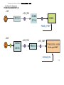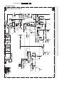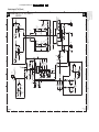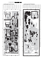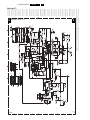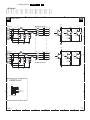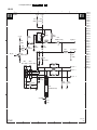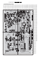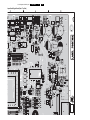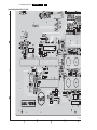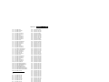
1
Colour TV
Chassis
TPS1.3A
LA
I_17610_000.eps
100408
Contents
Page
1. Technical Specifications, Connections, and Chassis
Overview
2
2. Safety Instructions, Warnings, and Notes
5
3. Directions for Use
6
4. Mechanical Instructions
7
5. Service Modes, Error Codes, and Fault Finding 10
6. Block Diagrams, Test Point Overviews, and
Waveforms
Wiring Diagram (37”)
13
Wiring Diagram (42”)
14
Wiring Diagram (47”)
15
Block Diagram Internal System (42”)
16
Block Diagram Internal System (47”)
17
Block Diagram Power Management (1)
18
Block Diagram Power Management (2)
19
External I/O (42” - 47”)
20
7. Circuit Diagrams and PWB Layouts
Diagram
Display Supply (32”)
(A) 21
Display Supply (37”-42”) (Part 1)
(A1) 23
Display Supply (37”-42”) (Part 2)
(A2) 24
Display Supply (47”)
(A) 26
SSB: DC / DC Power
(B01) 28
SSB: LIPS & Inverter I/F
(B02) 29
SSB: Tuner
(B03) 30
SSB: Video Input 1
(B04) 31
SSB: Video Input 2 (Side IO)
(B05) 32
SSB: DSUB Input
(B06) 33
SSB: HDMI Input 1
(B07) 34
SSB: HDMI Input 2 (Side IO)
(B08) 35
SSB: WT6702F (Standby MCU)
(B09) 36
SSB: Scaler MST98981CLD
(B10) 37
SSB: Flash ROM & Memory
(B11) 38
SSB: Key, IR BD, & ComPair I/F
(B12) 39
SSB: ITV I/F
(B13) 40
Contents
8.
9.
10.
11.
Page
SSB: Panel I/F
(B14) 41
SSB: Audio I/F
(B15) 42
SSB: Audio Amplifier
(B16) 43
SSB: Audio Out
(B17) 44
SSB: USB
(B18) 45
Side I/O Panel
(D) 56
Keyboard & Control Panel
(E) 58
IR & LED Panel
(J) 60
Alignments
63
Circuit Descriptions, Abbreviation List, and IC Data
Sheets
64
Abbreviation List
66
IC Data Sheets
68
Spare Parts List
71
Revision List
81
46-55
46-55
46-55
46-55
46-55
57
59
61
PWB
22
25
25
27
46-55
46-55
46-55
46-55
46-55
46-55
46-55
46-55
46-55
46-55
46-55
46-55
46-55
©
Copyright 2008 Koninklijke Philips Electronics N.V. Eindhoven, The Netherlands.
All rights reserved. No part of this publication may be reproduced, stored in a
retrieval system or transmitted, in any form or by any means, electronic,
mechanical, photocopying, or otherwise without the prior permission of Philips.
Published by CS 0864 BU CD Consumer Care
Printed in the Netherlands
Subject to modification
EN 3122 785 17610
EN 2
1.
Technical Specifications, Connections, and Chassis Overview
TPS1.3A LA
1. Technical Specifications, Connections, and Chassis Overview
1.1.3
Index of this chapter:
1.1 Technical Specifications
1.2 Connection Overview
1.3 Chassis Overview
Miscellaneous
Power supply
AC-input (V_ac)
Power consumption (W)
Notes:
• Figures can deviate due to the different set executions.
• Specifications are indicative (subject to change).
1.1
Technical Specifications
1.1.1
Vision
Power indicator
Auto power saving (W)
Display type
Screen size
Display area (HxV in mm)
Number of Pixels (HxV)
Pitch (HxV in mm)
Colour pixel arrangement
Display operating mode
Colour depth
Brightness (cd/m^2)
Viewing angle (CR>10)
Surface treatment
Electrical interface
Response Time (ms)
Contrast ratio
Backlight
Support Video Formats
1.1.2
:
:
:
:
:
:
:
:
:
:
:
:
:
:
:
:
:
:
:
:
:
:
:
:
:
:
:
:
:
:
:
LCD
42” (107 cm), 16:9
47” (119cm), 16.9
697.6 x 392.2 (42”)
1360 x 768
0.200x0.600 (37”)
0.227 x 0.681(42”)
0.761x0.761(47”)
RGB vertical stripe
Transmissive mode
Normally black
16.7M colours (8-bit)
500 (centre 1 pts, typ.)
R/L 178, U/D 178
Hard coating (3H)
LVDS
5 (37”and 42”)
8 (32”and 47”)
1000:1 (typ.)
16 EEFL
720x400
640x480
640x350
1024x768
1280x768
800x600
1280x800
1280x1024
1440x900
1680x1050
1920x1080
:
:
:
:
:
PAL
NTSC
SECAM
2x5 (32”)
2x10 (37”, 42”, & 47”)
Sound
Sound systems
Maximum power (W)
Horizontal scan
Horizontal
Vertical
Ambient conditions:
-Temperature
- Humidity
Dimensions (WxHxD in mm)
Weight (kg)
:
:
:
:
:
100 ~ 240
150 max (32”)
180 max (37”)
220 max (42”)
300 max (47”) (with
Smart Card)
: LED (On: Blue, Sleep
mode: Amber)
: < 18 with Smrt Crd,
< 3.5 without Smrt Crd
: 30 ~ 83 kHz
: 56 ~ 76 Hz
:
:
:
:
:
:
:
:
:
:
0 ~ 40 °C
20 to 70%
593x809x220 (32”)
666x929x262 (37”)
721x1033x262 (42”)
793x1150x310 (47”)
14.4 (32”)
19.8 (37”)
22 (42”)
33.4 (47”)
Technical Specifications, Connections, and Chassis Overview
1.2
Connection Overview
TPS1.3A LA
1.
EN 3
VGA: Video RGB - In
1
5
10
6
15
11
E_06532_002.eps
050404
Figure 1-3 VGA Connector
1
2
3
4
5
6
7
8
9
10
11
12
13
14
15
I_17610_002.eps
280308
Figure 1-1 Rear I/O connections
Note: The following connector colour abbreviations are used
(acc. to DIN/IEC 757): Bk= Black, Bu= Blue, Gn= Green, Gy=
Grey, Rd= Red, Wh= White, and Ye= Yellow.
1.2.1
Rear Connections
1
2
E_06532_017.eps
250505
Figure 1-2 HDMI (type A) connector
1
2
3
4
5
6
7
8
9
10
11
12
13
14
15
16
17
18
19
20
- D2+
- Shield
- D2- D1+
- Shield
- D1- D0+
- Shield
- D0- CLK+
- Shield
- CLK- n.c.
- n.c.
- DDC_SCL
- DDC_SDA
- Ground
- +5V
- HPD
- Ground
Data channel
Gnd
Data channel
Data channel
Gnd
Data channel
Data channel
Gnd
Data channel
Data channel
Gnd
Data channel
DDC clock
DDC data
Gnd
Hot Plug Detect
Gnd
0.7 VPP / 75 ohm
0.7 VPP / 75 ohm
0.7 VPP / 75 ohm
j
j
j
Gnd
Gnd
Gnd
Gnd
+5 V
Gnd
H
H
H
H
j
H
DDC data
0-5V
0-5V
DDC clock
j
j
j
j
CVI 1 & 2: Cinch: Video YPbPr - In, Audio - In
Gn - Video Y
1 VPP / 75 ohm
Bu - Video Pb
0.7 VPP / 75 ohm
Rd - Video Pr
0.7 VPP / 75 ohm
Wh - Audio L
0.5 VRMS / 10 kohm
Rd - Audio R
0.5 VRMS / 10 kohm
HDMI1 & 2: Digital Video, Digital Audio - In
19
18
- Video Red
- Video Green
- Video Blue
- n.c.
- Ground
- Ground Red
- Ground Green
- Ground Blue
- +5V_dc
- Ground Sync
- n.c.
- DDC_SDA
- H-sync
- V-sync
- DDC_SCL
j
H
j
j
H
j
j
H
j
j
H
j
j
jk
H
j
j
H
1.2.2
jq
jq
jq
jq
jq
Service Connector (ComPair)
1 - SDA-S
I2C Data (0 - 5 V)
2 - SCL-S
I2C Clock (0 - 5 V)
3 - Ground
Gnd
jk
j
H
Audio Out: Cinch: Audio - Out
Rd - Audio R
0.5 VRMS / 10 kohm
Wh - Audio L
0.5 VRMS / 10 kohm
kq
kq
Side AV
I_17610_003.eps
280308
Figure 1-4 Side AV
AV Input: Cinch: Video CVBS - In, Audio - In
Rd - Audio R
0.5 VRMS / 10 kohm
Wh - Audio L
0.5 VRMS / 10 kohm
Ye - Video CVBS
1 VPP / 75 ohm
AV Input: S-Video (Hosiden): Video Y/C - In
1 - Ground Y
Gnd
2 - Ground C
Gnd
3 - Video Y
1 VPP / 75 ohm
4 - Video C
0.3 VPPP / 75 ohm
jq
jq
jq
H
H
j
j
Cinch: Mono Speaker- Out
Bu - Audio - Mono
0.5 VRMS / 10 kohm
kq
Cinch: S/PDIF - Out
Bk - Coaxial
kq
0.4 - 0.6VPP / 75 ohm
EN 4
TPS1.3A LA
Technical Specifications, Connections, and Chassis Overview
Chassis Overview
A
B
E
1.3
1.
J
I_17610_004.eps
100408
Figure 1-5 Chassis Overview
Safety Instructions, Warnings, and Notes
TPS1.3A LA
2.
EN 5
2. Safety Instructions, Warnings, and Notes
Index of this chapter:
2.1 Safety Instructions
2.2 Warnings
2.3 Notes
•
2.1
Safety Instructions
Safety regulations require the following during a repair:
• Connect the set to the Mains/AC Power via an isolation
transformer (> 800 VA).
• Replace safety components, indicated by the symbol h,
only by components identical to the original ones. Any
other component substitution (other than original type) may
increase risk of fire or electrical shock hazard.
Safety regulations require that after a repair, the set must be
returned in its original condition. Pay in particular attention to
the following points:
• Route the wire trees correctly and fix them with the
mounted cable clamps.
• Check the insulation of the Mains/AC Power lead for
external damage.
• Check the strain relief of the Mains/AC Power cord for
proper function.
• Check the electrical DC resistance between the Mains/AC
Power plug and the secondary side (only for sets that have
a Mains/AC Power isolated power supply):
1. Unplug the Mains/AC Power cord and connect a wire
between the two pins of the Mains/AC Power plug.
2. Set the Mains/AC Power switch to the "on" position
(keep the Mains/AC Power cord unplugged!).
3. Measure the resistance value between the pins of the
Mains/AC Power plug and the metal shielding of the
tuner or the aerial connection on the set. The reading
should be between 4.5 Mohm and 12 Mohm.
4. Switch "off" the set, and remove the wire between the
two pins of the Mains/AC Power plug.
• Check the cabinet for defects, to prevent touching of any
inner parts by the customer.
2.2
•
2.3.2
•
•
•
•
•
•
•
•
All ICs and many other semiconductors are susceptible to
electrostatic discharges (ESD w). Careless handling
during repair can reduce life drastically. Make sure that,
during repair, you are connected with the same potential as
the mass of the set by a wristband with resistance. Keep
components and tools also at this same potential. Available
ESD protection equipment:
– Complete kit ESD3 (small tablemat, wristband,
connection box, extension cable and earth cable) 4822
310 10671.
– Wristband tester 4822 344 13999.
Be careful during measurements in the high voltage
section.
Never replace modules or other components while the unit
is switched "on".
When you align the set, use plastic rather than metal tools.
This will prevent any short circuits and the danger of a
circuit becoming unstable.
2.3
Notes
2.3.1
General
•
Measure the voltages and waveforms with regard to the
chassis (= tuner) ground (H), or hot ground (I), depending
on the tested area of circuitry. The voltages and waveforms
shown in the diagrams are indicative. Measure them in the
All resistor values are in ohms, and the value multiplier is
often used to indicate the decimal point location (e.g. 2K2
indicates 2.2 kohm).
Resistor values with no multiplier may be indicated with
either an "E" or an "R" (e.g. 220E or 220R indicates 220
ohm).
All capacitor values are given in micro-farads (μ= x10-6),
nano-farads (n= x10-9), or pico-farads (p= x10-12).
Capacitor values may also use the value multiplier as the
decimal point indication (e.g. 2p2 indicates 2.2 pF).
An "asterisk" (*) indicates component usage varies. Refer
to the diversity tables for the correct values.
The correct component values are listed in the Spare Parts
List. Therefore, always check this list when there is any
doubt.
BGA (Ball Grid Array) ICs
Introduction
For more information on how to handle BGA devices, visit this
URL: www.atyourservice.ce.philips.com (needs subscription,
not available for all regions). After login, select "Magazine",
then go to "Repair downloads". Here you will find Information
on how to deal with BGA-ICs.
BGA Temperature Profiles
For BGA-ICs, you must use the correct temperature-profile,
which is coupled to the 12NC. For an overview of these profiles,
visit the website www.atyourservice.ce.philips.com (needs
subscription, but is not available for all regions)
You will find this and more technical information within the
"Magazine", chapter "Repair downloads".
For additional questions please contact your local repair help
desk.
Warnings
•
Schematic Notes
•
2.3.3
Service Default Mode (see chapter 5) with a colour bar
signal and stereo sound (L: 3 kHz, R: 1 kHz unless stated
otherwise) and picture carrier at 475.25 MHz for PAL, or
61.25 MHz for NTSC (channel 3).
Where necessary, measure the waveforms and voltages
with (D) and without (E) aerial signal. Measure the
voltages in the power supply section both in normal
operation (G) and in stand-by (F). These values are
indicated by means of the appropriate symbols.
Manufactured under license from Dolby Laboratories.
"Dolby", "Pro Logic" and the "double-D symbol", are
trademarks of Dolby Laboratories.
2.3.4
Lead-free Soldering
Due to lead-free technology some rules have to be respected
by the workshop during a repair:
• Use only lead-free soldering tin Philips SAC305 with order
code 0622 149 00106. If lead-free solder paste is required,
please contact the manufacturer of your soldering
equipment. In general, use of solder paste within
workshops should be avoided because paste is not easy to
store and to handle.
• Use only adequate solder tools applicable for lead-free
soldering tin. The solder tool must be able:
– To reach a solder-tip temperature of at least 400°C.
– To stabilize the adjusted temperature at the solder-tip.
– To exchange solder-tips for different applications.
• Adjust your solder tool so that a temperature of around
360°C - 380°C is reached and stabilized at the solder joint.
Heating time of the solder-joint should not exceed ~ 4 sec.
Avoid temperatures above 400°C, otherwise wear-out of
tips will increase drastically and flux-fluid will be destroyed.
EN 6
•
3.
TPS1.3A LA
Directions for Use
example below it is 2008 week 10). The 6 last digits contain the
serial number.
To avoid wear-out of tips, switch "off" unused equipment or
reduce heat.
Mix of lead-free soldering tin/parts with leaded soldering
tin/parts is possible but PHILIPS recommends strongly to
avoid mixed regimes. If this cannot be avoided, carefully
clear the solder-joint from old tin and re-solder with new tin.
MODEL
: 32PF9968/10
PROD.NO: AG 1A0617 000001
2.3.5
S
Alternative BOM identification
The third digit in the serial number (example:
AG2B0335000001) indicates the number of the alternative
B.O.M. (Bill Of Materials) that has been used for producing the
specific TV set. In general, it is possible that the same TV
model on the market is produced with e.g. two different types
of displays, coming from two different suppliers. This will then
result in sets which have the same CTN (Commercial Type
Number; e.g. 28PW9515/12) but which have a different B.O.M.
number.
By looking at the third digit of the serial number, one can
identify which B.O.M. is used for the TV set he is working with.
If the third digit of the serial number contains the number "1"
(example: AG1B033500001), then the TV set has been
manufactured according to B.O.M. number 1. If the third digit is
a "2" (example: AG2B0335000001), then the set has been
produced according to B.O.M. no. 2. This is important for
ordering the correct spare parts!
For the third digit, the numbers 1...9 and the characters A...Z
can be used, so in total: 9 plus 26= 35 different B.O.M.s can be
indicated by the third digit of the serial number.
Identification: The bottom line of a type plate gives a 14-digit
serial number. Digits 1 and 2 refer to the production centre (e.g.
BZ is Suzhou), digit 3 refers to the B.O.M. code, digit 4 refers
to the Service version change code, digits 5 and 6 refer to the
production year, and digits 7 and 8 refer to production week (in
3. Directions for Use
You can download this information from the following websites:
http://www.philips.com/support
http://www.p4c.philips.com
MADE IN BELGIUM
220-240V ~ 50/60Hz
128W
VHF+S+H+UHF
BJ3.0E LA
E_06532_024.eps
260308
Figure 2-1 Serial number (example)
2.3.6
Board Level Repair (BLR) or Component Level Repair
(CLR)
If a board is defective, consult your repair procedure to decide
if the board has to be exchanged or if it should be repaired on
component level.
If your repair procedure says the board should be exchanged
completely, do not solder on the defective board. Otherwise, it
cannot be returned to the O.E.M. supplier for back charging!
2.3.7
Practical Service Precautions
•
•
It makes sense to avoid exposure to electrical shock.
While some sources are expected to have a possible
dangerous impact, others of quite high potential are of
limited current and are sometimes held in less regard.
Always respect voltages. While some may not be
dangerous in themselves, they can cause unexpected
reactions that are best avoided. Before reaching into a
powered TV set, it is best to test the high voltage insulation.
It is easy to do, and is a good service precaution.
Mechanical Instructions
TPS1.3A LA
4.
EN 7
4. Mechanical Instructions
Index of this chapter:
4.1 Cable Dressing
4.2 Service Positions
4.3 Assy/Panel Removal
4.4 Set Re-assembly
4.1
Notes:
• Figures below can deviate slightly from the actual situation,
due to the different set executions.
• Follow the disassemble instructions in described order.
They apply to the 32" model, but the described method is
comparable for the other screen sizes.
Cable Dressing
I_17610_005.eps
280308
Figure 4-1 Cable dressing (42” model)
EN 8
4.2
4.
TPS1.3A LA
Mechanical Instructions
Service Positions
4.3.2
1. Refer to next figure.
2. Unscrew two screws[1]
3. Release clips [2].
4. Unplug connector [3] and remove the board.
When defective, replace the whole unit
For easy servicing of this set, there are a few possibilities
created:
• The buffers from the packaging.
• The original aluminium stands.
• Foam bars (created for Service).
4.2.1
Keyboard Control Board
Foam Bars
1
1
2
3
I_17610_006.eps
280308
Figure 4-3 Keyboard control board
4.3.3
1
IR Board
1. Refer to next figure.
2. Unplug the connector [1].
3. Release clips [2] and remove the IR board.
When defective, replace the whole unit.
Required for sets
42"
2
1
I_17610_007.eps
280308
Figure 4-4 IR board
4.3.4
E_06532_018.eps
171106
Figure 4-2 Foam bars
Speakers
1. Refer to next two figures.
2. Unplug the connectors [1].
3. Remove the screws [2].
The foam bars (order code 3122 785 90580 for two pieces) can
be used for all types and sizes of Flat TVs. See figure “Foam
bars” for details. Sets with a display of 42” and larger, require
four foam bars [1]. Ensure that the foam bars are always
supporting the cabinet and never only the display. Caution:
Failure to follow these guidelines can seriously damage the
display!
By laying the TV face down on the (ESD protective) foam bars,
a stable situation is created to perform measurements and
alignments. By placing a mirror under the TV, you can monitor
the screen.
1
2
1
I_17610_008.eps
280308
Figure 4-5 Speaker-1
4.3
Assy/Panel Removal
4.3.1
Rear Cover
Warning: Disconnect the mains power cord before you remove
the rear cover.
1. Place the TV set upside down on a table top, using the
foam bars (see part "Service Position").
2. Remove the screws that secure the rear cover and the
stand (if mounted). The screws are located at the top,
bottom, left and right sides.
3. Lift the rear cover from the cabinet. Make sure that wires
and flat foils are not damaged during cover removal.
1
2
1
I_17610_008.eps
280308
Figure 4-6 Speaker-2
Mechanical Instructions
4.3.5
TPS1.3A LA
4.
EN 9
Power Supply Board
1.
2.
3.
4.
Refer to next figure.
Unplug all the connectors [1].
Remove the fixation screws [2]
Remove the board.
1
2
1
2
1
2
1
1
I_17610_011.eps
280308
Figure 4-8 SB removal
2
1
4.4
Set Re-assembly
To re-assemble the whole set, execute all processes in reverse
order.
I_17610_009.eps
280308
Figure 4-7 Power supply board
4.3.6
Scaler Board (SB)
Caution: it is absolutely mandatory to remount all different
screws at their original position during re-assembly. Failure to
do so may result in damaging the SB.
Removing the SB
1. See the figure ”SB removal”.
2. Unplug all of the cables [1].
3. Removed the parker screws [2].
Notes:
• While re-assembling, make sure that all cables are placed
and connected in their original position. See figure "Cable
dressing".
• Pay special attention not to damage the EMC foams at the
SB shields. Make sure, that EMC foams are put correctly
on their places.
EN 10
5.
TPS1.3A LA
Service Modes, Error Codes, and Fault Finding
5. Service Modes, Error Codes, and Fault Finding
Index of this chapter:
5.1 Test Points
5.2 Service Mode
5.3 Error Codes
5.4 Software Upgrading
5.1
Test Points
This chassis is NOT equipped with test points in the service
printing. These test points are NOT specifically mentioned in
the service manual.
5.2
Service Mode
5.2.1
Factory Mode or Service Alignment Mode (SAM)
How to Enter
To enter the Factory mode, use the following method:
• Press on the remote control the code “062596” directly
followed by the “DISPLAY/OUT” key.
• Press the “MENU” key and select “2K8 CH V1 00” to enter
the “Factory” mode as shown in the next two pictures.
Caution: This function is available for development and
service personnel only, not for end customers.
I_17610_012.eps
280308
Figure 5-2 Factory mode menu 2)
How to EXIT
Choose “EXIT”, then press the “MENU” button on the remote
control.
After entering the Factory mode, the following screen is visible,
the values can be adjusted according to the requested (see
Chapter 8).
5.2.2
Customer Service Mode (CSM)
Purpose
When a customer is having problems with his TV-set, he can
call his dealer or the Customer Helpdesk. The service
technician can then ask the customer to activate the CSM, in
order to identify the status of the set. Now, the service
technician can judge the severity of the complaint. In many
cases, he can advise the customer how to solve the problem,
or he can decide if it is necessary to visit the customer. The
CSM is a read only mode; therefore, modifications in this mode
are not possible.
How to Activate CSM
Key in the code ”123654” via the standard RC transmitter.
I_17610_010.eps
280308
Figure 5-1 Factory mode menu (1)
How to Navigate
By mean of the “CURSOR-DOWN/UP” knob on the RCtransmitter on the screen.
Service Modes, Error Codes, and Fault Finding
Contents of CSM
I_17610_013.eps
280308
Figure 5-3 CSM Menu
Menu Explanation
1. Set Type. Type number and region.
2. Production code. Product serial no.
3. SW naming main-processor. Software cluster and
version is displayed.
4. SW other-processor. Not applicable.
5. Code 1. Error buffer contents.
6. Code 2. Error buffer contents.
7. Key (HDCP): Indicates if the HDCP-key are valid (HDMI).
8. NVM-Name: Indicates the used LCD panel type and region
(NVM content and main SW depend on the used LCD
panel).
How to exit
Press ”MENU” on the RC-transmitter.
TPS1.3A LA
5.
EN 11
EN 12
5.3
5.
TPS1.3A LA
Service Modes, Error Codes, and Fault Finding
Error Codes
The error code buffer contains all errors detected since the last
time the buffer was erased. The buffer is written from left to
right. When an error occurs that is not yet in the error code
buffer, it is displayed at the left side and all other errors shift one
position to the right.
TO TV
TO
UART SERVICE
CONNECTOR
TO
I2C SERVICE
CONNECTOR
TO
UART SERVICE
CONNECTOR
Basically there are five kind of errors:
Error code
Event
0x01
Audio Decode Error
0x02
IIC bus Error
0x03
Tuner Error
0x04
NVRAM Error
0x05
Scaler Chip Error
ComPair II
RC in
RC out
Multi
function
Optional Power Link/ Mode
Switch
Activity
I 2C
RS232 /UART
PC
5.4
Software Upgrading
5.4.1
ComPair
Introduction
ComPair (Computer Aided Repair) is a Service tool for Philips
Consumer Electronics products. and offers the following:
1. ComPair features TV software upgrade possibilities.
2. ComPair helps you to quickly get an understanding on how
to repair the chassis in a short and effective way (this
feature is not supported in this chassis).
3. ComPair allows very detailed diagnostics and is therefore
capable of accurately indicating problem areas. You do not
have to know anything about I2C or UART commands
yourself, because ComPair takes care of this this feature is
not supported in this chassis).
4. ComPair speeds up the repair time since it can
automatically communicate with the chassis (when the uP
is working) and all repair information is directly available
this feature is not supported in this chassis).
Specifications
ComPair consists of a Windows based fault finding program
and an interface box between PC and the (defective) product.
The (new) ComPair II interface box is connected to the PC via
an USB cable. For the TV chassis, the ComPair interface box
and the TV communicate via a bi-directional cable via the
service connector(s).
How to Connect
This is described in the ComPair chassis fault finding database.
ComPair II Developed by Philips Brugge
HDMI
I2C only
Optional power
5V DC
E_06532_036.eps
150208
Figure 5-4 ComPair II interface connection
Caution: It is compulsory to connect the TV to the PC as
shown in the picture above (with the ComPair interface in
between), as the ComPair interface acts as a level shifter. If
one connects the TV directly to the PC (via UART), ICs will be
blown!
How to Order
ComPair II order codes:
• ComPair II interface: 312278591020.
• For SW see Philips service website.
• ComPair I2C interface cable: 312278590004 or
312278590630.
Note: If you encounter any problems, contact your local
support desk.
Block Diagrams, Test Point Overviews, and Waveforms
TPS1.3A LA
6.
13
6. Block Diagrams, Test Point Overviews, and Waveforms
Wiring Diagram (37”)
WIRING DIAGRAM 37”
I_17610_018.eps
080408
Block Diagrams, Test Point Overviews, and Waveforms
TPS1.3A LA
6.
14
Wiring Diagram (42”)
Wiring Diagram (42”)
I_17610_019.eps
100408
Block Diagrams, Test Point Overviews, and Waveforms
TPS1.3A LA
6.
15
Wiring Diagram (47”)
Wiring Diagram (47”)
I_17610_020.eps
080408
Block Diagrams, Test Point Overviews, and Waveforms
TPS1.3A LA
6.
16
Block Diagram Internal System (42”)
Key Bd
42PFL3403 Internal System Block Diagram
CN7301
C
N
9
0
2
X’FRM
T802
IR Bd
CN7302
L-R Speaker
CN6101
CN6102
LIPS Bd
C
N
7
2
0
1
AMP
TPA3120D
U6102
STDBY MCU
WT6702
1st_SPI
S25FL004A
NVRAM
M24C32
U4101
U4402
U4203
LCD Panel
X’FRM
T902/3
X’FRM
T901
Super LIPS
C
N
7
5
0
1
LVDS
HDMI_DDC
M24C02
DSUB_EDID
M24C02
U1501
U1401
HDMI DDC
M24C02
U1502
715T2690-1
MST98981CLDA
(MSPH102)
U4201
DDR
HY5DU281622
U4401(4402)
Tuner
Z017D (93)
W017D (98)
TU1101
715T2878-1
I_17610_021.eps
100408
Block Diagrams, Test Point Overviews, and Waveforms
TPS1.3A LA
6.
17
Block Diagram Internal System (47”)
Key Bd
47PFL3403 Internal System Block Diagram
CN7301
C
N
9
0
5
C
N
9
0
3
C
N
9
0
2
IR Bd
CN7302(7P)
L-R Speaker
CN6101
CN6102
LIPS Bd
C
N
7
2
0
1
AMP
TPA3120D
U6102
STDBY MCU
WT6702
1st_SPI
S25FL004A
NVRAM
M24C32
U4101
U4402
U4203
X’FRM
T905
LCD Panel
C
N
7
5
0
1
LVDS
MST98981CLDA
(MSPH102)
U4201
DDR
HY5DU281622
U4401(4402)
X’FRM
L903
HDMI_DDC
M24C02
DSUB_EDID
M24C02
U1501
U1401
HDMI DDC
M24C02
U1502
715T2828-1
Tuner
Z017D (93)
W017D (98)
TU1101
715T2878-1
I_17610_022.eps
100408
Block Diagrams, Test Point Overviews, and Waveforms
TPS1.3A LA
6.
18
Block Diagram Power Management (1)
POWER MANAGEMENT (1)
+5V_STBY
AIC1550
U7101
+3.3V_STBY
WT6702F
U4101
+3V3_HD_SW
+3V3_SW
S14835
Q7103
+5V_SW
AME8815
U7103
FB1503
PI3HDMI1212ABE
U1503
1st SPI Flash ROM
U4402
AIC1550
U7104
S14835
Q7106
+5V_SW1
AME8815
U7105
AME1117
U7106
+1V2
MST98981CLD-LF
U4201
+3V3
+2V6
HY5DU281622FTP5
DDR
U4401
TUNER
TU1101
I_17610_023.eps
080408
Block Diagrams, Test Point Overviews, and Waveforms
TPS1.3A LA
6.
19
Block Diagram Power Management (2)
POWER MANAGEMENT (2)
+12V
+12V_SW
SI4835
FB7105
PANEL
Q7114
PANEL_PWR
+24V
+24V_SW
+24V_AMP
SI4835
Q6105
FB6103
TPA3123D2 U6102
Audio post-AMP
SOUND_EN
I_17610_024.eps
080408
Block Diagrams, Test Point Overviews, and Waveforms
TPS1.3A LA
6.
20
External I/O (42” - 47”)
EXTERNAL I/O FOR 42_47PFL3403
SIF0
Tuner
HDMI 1
CVBS0
DVI-D
HDMI 2
R1,G1,B1
D-SUB
UART1
AUL2, AUR2
Com Pair
PC Audio
Cloning
CVBS
CVBS1
S-Video
Y0,C0
(ITV-1)
AUL1, AUR1
MST98981CLD
CVBS Audio
CVI-1 (Video)
CVI-2 (Video)
CVI-1 (Audio)
(5P)
Y,Pb,Pr (R2,G2,B2)
Y,Pb,Pr (R0,G0,B0)
AUL0, AUR0
Video I/F
(ITV-2)
AUL3, AUR3
CVBS2,Y1,C1
(10P)
SIDE AV
TPA6203A
1W AMP
AUL1, AUR1
CVI-2 (Audio)
HP(CN1303)
Bathroom
Speaker (ITV-2)
Remark : Reserve only for ITV function
I_17610_025.eps
080408
Circuit Diagrams and PWB Layouts
TPS1.3A LA
7.
21
7. Circuit Diagrams and PWB Layouts
Display Supply (32”)
1
2
3
4
7
6
5
9
8
1
+400V_F
FB904
2
Q901
SPW16N50
LS4148
B
P6KE160A
2
2
R916
IC901
0R
1
2
3
4
R984
12K
!
CONN_NC
S
6
S
470nF
7
S
BP/M
2
8
S EN/UV
1
R912
R908
R911
R910
D
ZD981
RLZ15B
R999
R985
!
1
C901
SG902
GS41-201MA
+
C983
0.1uF
10K
C988
10UF/50V_NC
C989
0.1uF
1
2
Jump
IC982
TL431
RLZ5.1B_NC
2
1
R992
!
ZD966
RLZ15B
R950
100K
1
2
HD955
Heatsink
STANDBY_IN
1
Q993
2N7002
D
3
4
R902
330K
HQ951
Heatsink
C950
1000pF/250V_NC
+400V_F
R901
330K
+400V
2
R903
330K
ZD965
RLZ27B
1
!
!
C
1
3
!
Q992
2N7002
18K_1%
R993
22K_1%
C906
1000pF/250V
470nF
R987
100R
ZD982
!
FB906
R909
680R_1%
!
D
R988
390K
1
1 L901
13mH
SG901
GS41-201MA
C982
100pF
+12V
R986
100R
R991
11K_1%
1
4
2
2
1
2
3
+24V_A
R990
0R
R995
3.3K
IC932
TCET1103G
1M
1M_1%
1M_1%
EF-20
!
4
R913
18K_1%
C915
1nF
C913
330nF
+
R983
220R
5
C981
33uF_50V
TNY277
1M_1%
33K
C914
1uF
3.5uH
10R
+
2
5
+400V_F
C904
+
2
2
IC931
R915
0.1R_1W
C912
220pF
R907
33K
2
1
8
7
6
B
3
1
1
CN904
FB901
R982
47R
R917
2
4
R996
1N4148
SG6961
220R
Jump
D981
R998
4
!
51K
3
R906
200K_NC
C902
470pF
C903
470pF
2
D935 SP1060
3
UG1007
47R
INV
VCC
COMP OUT
MOT GND
CS
ZCD
!
10
9
8
7
6
5
SG904
GS41-201MA
L902
13mH
+5VSB
L980
1
T901
D980
1
4
1
1
!
C910
10pF_NC
C984
2
10nF/100V
2
2
2 1
Bead
1
R919
3
SG903
GS41-201MA
1
!
3
2
10R
FB980
ZD980
2
C960
220pF/1KV_NC
1
2
HQ901
Heatsink
2
1
D903
R918
1
10uF/50V
HD935
Heatsink
C959
33uF 50V
C986
47uF 25V
C909
+
3
C911
0.1uF
C916
10pF
RGP10D
2
BEAD
2
L905
C951
2.2nF/1KV_NC
+400V
2
-
R905
47K
L904
BEAD
4
+
1
1
2
1
3
C953
2.2nF/500V
1
+
BU1006A-E3/45
C907
120uF450V
VCC_PI
1
2
1
7
8
9
1
VCC_PFC
BD901
ZD902
D982
2
RV902
HD902
Heatsink
TVR14561KFC4FY_NC
3
4
+
P6KE440A_NC
L906
PFC Choke_230uH
C905
1uF/450V
Jump
1
STTH8L06FP
A
2
1
Jump
C985
2200uF 10V
1
C980
1.5nF/500V
L903
BEAD_NC
2
FB905
D902
5
6
2
3
4
1
!
1
HBD901
Heatsink
1
2
A
A
+400V
2
FB902
2
Jump
HQ952
Heatsink
t
NR901
2
1
RFmin_FB
2
3
CN901
C933
220pF
C932
0.47uF
SOCKET
R958
18K_1%
C936
0.1uF
3
1
+
C943
C945
0.1uF
C944
470UF35V
1000UF35V
R957
2.7K
1
2
3
4
5
6
7
8
Css
VBOOT
DELAY
HVG
CF
OUT
RFmin
N.C.
STBY
Vcc
ISEN
LVG
LINE
GND
DIS PFC_STOP
16
15
14
13
12
11
10
9
R974
5.1K
R975
5.1K_NC
E
VCC_PFC
D952
LS4148
R936 10R
10
9
C954
2.2nF/500V_NC
Q952
2SK4097LS
11
12
1
+
C937
0.1uF
L6599D
R962
22R
L931
3.5uH
+12V
2
D956
SP1060
7
8
R963
51K
C939
10uF/50V
+12V_F
3
IC951
RFmin
STBY
R959
1M
+
+
1
!
2
SP20100
14
13
1
F901
T5AH/250V
16
R955
2M
3.9K_1%
R966
2
4
3
+24V
3.0uH
D955
T902
3
R961
51K
!
2
1
+24V_F
L971
1
2
22R
2
RV901
TVR14561KFC4FY
1
Q951
2SK4097LS
R960
R954
2M
1
!
2
!
F902
NC
LS4148
3
1
D951
1
R953
2M
SCK101R55LSY
E
11
DISPLAY SUPPLY (32”)
A
C
10
15
+
C946
470uF/25V
C947
220uF/25V
R976
1.2K_NC
ERL35
C941
R964
27nF/1000V
1K
C934
1uF
R956
24K
C935
0.1uF
C940
1nF
C952
1nF_NC
C938
0.1uF_NC
R965
0.33R_1W
F
F
+24V_A
+12V
+24V
+24V
D914
CN903
2
+12V
1
2
3
2
Q988
2N7002
2
STANDBY_IN
R997
1K
INVERTER-ON-OFF
BRIGHT-ADJ
G
WAFER 2.5MM 13P 64842
C958
0.1uF_NC
STANDBY_IN
1
2
C987
0.1uF
R973
1.96K _1%
R994
100K?
2
1
RLZ27B_NC
WAFER 2.5MM 12P
1
R977
2.4K_1/2W
1
2
1
IC953
TL431
IC991
TCET1103G
R981
47K_1%
1K_NC
3
2
+5VSB
4.7K
C957
0.1uF_NC
+24V
1
2
3
4
5
6
7
8
9
10
11
12
13
3
0.1uF_NC
R972
20.5K_1%
R970
R980
!
1
1
C949
ZD935
RLZ15B
R971
Jump
68nF
1
C948
ZD967
R945
10K
1INVERTER-ON-OFF
2 BRIGHT-ADJ
3
4
5
6
7
8
9
10 STANDBY
11
+5VSB
12
1
2
3
4
5
6
7
8
9
10
11
12
To panel
10R
+24V_F
2
3
G
VCC_PI
1
1
2
3
4
5
6
7
8
9
10
11
12
13
2
IC952
TCET1103G
C942
1nF_NC
3
2
0R
Q945
BC337
R937
R969
3.3K
To scaler
R968
10K
4
!
RFmin_FB
1
R967
100R_NC
4
STBY
Jump wire
0.1uF_NC
R989
RFmin
C956
CN902
VCC_PFC
H
H
I_17610_031.eps
080408
715T2870-1
1
2
3
4
5
6
7
8
9
10
11
BD901
C901
C902
C903
C904
C905
C906
C907
C909
C910
C911
C912
C913
C914
C915
C916
C932
C933
C934
C935
C936
C937
C938
C939
C940
C941
C942
C943
C944
C945
C946
C947
C948
C949
C950
C951
C952
C953
C954
C956
C957
C958
C959
C960
C980
C981
C982
C983
C984
C985
C986
C987
C988
C989
CN901
CN902
CN903
CN904
D902
D903
D914
D935
D951
D952
D955
D956
D980
D981
D982
F901
F902
FB901
FB902
FB904
FB905
FB906
FB980
HBD901
HD902
HD935
HD955
HQ901
HQ951
HQ952
IC901
IC931
IC932
IC951
IC952
IC953
IC982
IC991
L901
L902
L903
L904
L905
L906
L931
L971
L980
A1
D2
C2
C1
C2
A2
D5
A6
B4
B3
B3
C4
C3
C3
C4
B3
E3
E3
F3
F4
E5
E5
F4
E5
F5
F6
G2
E8
E9
E9
E8
E9
G3
G3
D5
A7
F5
A6
E6
F9
G9
G8
A8
B5
B7
C7
C7
C7
B9
B9
B10
H6
C7
C9
E1
G8
F10
C1
A5
B4
F9
B9
D5
E5
D8
E8
B7
B8
A8
E1
E1
C1
A2
A5
A6
D5
B9
A1
A4
A9
D7
B6
D6
D6
B3
C6
C8
E4
G2
G3
C9
G6
C2
B2
A2
B1
B2
A3
E8
D8
B10
NR901
Q901
Q945
Q951
Q952
Q988
Q992
Q993
R901
R902
R903
R905
R906
R907
R908
R909
R910
R911
R912
R913
R915
R916
R917
R918
R919
R936
R937
R945
R950
R953
R954
R955
R956
R957
R958
R959
R960
R961
R962
R963
R964
R965
R966
R967
R968
R969
R970
R971
R972
R973
R974
R975
R976
R977
R980
R981
R982
R983
R984
R985
R986
R987
R988
R989
R990
R991
R992
R993
R994
R995
R996
R997
R998
R999
RV901
RV902
SG901
SG902
SG903
SG904
T901
T902
ZD902
ZD935
ZD965
ZD966
ZD967
ZD980
ZD981
D1
B5
G5
D6
E6
G6
D10
D9
D2
D2
D1
B3
B3
C3
C3
D4
C5
C5
C4
C4
C5
B4
C4
B4
B4
E5
G5
G6
D10
D4
E4
E4
F4
E3
E3
E2
E5
E6
E5
E6
F5
F6
E3
G2
G3
G3
G3
G4
G4
H4
E9
E10
E9
G9
G6
G4
C7
C9
C7
C9
C10
C11
C7
G1
C9
C9
C9
D9
H7
C9
B8
G9
B7
C8
E2
A5
C1
C2
B1
B2
B8
E7
A6
G5
C10
C11
H2
B7
C7
Circuit Diagrams and PWB Layouts
TPS1.3A LA
7.
22
Layout Display Supply Panel (32”) (Top Side)
BD901
C901
C902
C903
C904
C905
C906
C907
C909
C939
C941
C943
D2
C3
D3
D2
D3
D1
B3
C3
C1
C1
B2
A1
C944
C946
C947
C950
C951
C953
C954
C959
C960
C980
C981
C984
715T2870-1
A1
A2
A1
D1
B3
B3
B1
B4
C2
B3
B4
A3
C985
C986
C988
CN901
CN902
CN903
CN904
D902
D914
D935
D955
D956
A3
A4
C3
D3
A3
A1
C3
B2
A3
A3
A2
A2
D980 B3
D982 B3
F901
D3
F902
D3
FB901 C3
FB902 D2
FB904 C3
FB905 B3
FB906 B3
FB980 A3
HBD901C2
HD902 B2
HD935
HD955
HQ901
HQ951
HQ952
IC931
IC932
IC952
IC953
IC982
IC991
J911
A3
A2
C2
B1
B1
B3
B3
B1
A1
A3
B3
B2
J912
J913
J914
J915
J916
J917
J918
J919
J920
J921
J922
J923
C2
C2
C1
C1
C1
B1
B1
B3
C1
C1
A3
A3
J924
J925
J926
J927
J928
J929
J930
L901
L902
L903
L904
L905
Layout Display Supply Panel (32”) (Bottom Side)
A2
A2
A2
A2
A1
A1
A3
C3
C2
D2
C2
D2
L906
L931
L971
L980
NR901
Q901
Q945
Q951
Q952
R915
R955
R965
D2
A2
A1
A4
C3
C2
B3
B1
B1
C2
C1
B1
R971
R976
R977
R980
R987
RV901
RV902
SG901
SG902
SG903
SG904
T901
A1
A3
A3
B3
A3
D3
C3
C3
D3
C2
D2
B3
T902
B1
ZD902 C3
ZD980 B3
I_17610_032.eps
080408
C910
C911
C912
C913
C914
C915
C916
C932
C933
C934
C935
C1
C1
C1
C1
C1
C1
C1
C1
C1
C1
C1
C936
C937
C938
C940
C942
C945
C948
C949
C952
C956
C957
C1
C1
C1
C1
C1
A1
A1
A1
C1
A3
A3
715T2870-1
C958
C982
C983
C987
C989
D903
D951
D952
D981
IC901
IC951
A3
B3
B3
A3
A3
C2
C1
C1
B3
C1
C1
Q988
Q992
Q993
R901
R902
R903
R905
R906
R907
R908
R909
B3
A3
A3
C3
C3
C3
C1
C1
C1
C1
C1
R910
R911
R912
R913
R916
R917
R918
R919
R936
R937
R945
D1
C1
C1
C1
C2
C1
C2
C2
C1
B3
B3
R950
R953
R954
R956
R957
R958
R959
R960
R961
R962
R963
A3
C1
C1
C1
C1
C1
C1
C1
C1
C1
C1
R964
R966
R967
R968
R969
R970
R972
R973
R974
R975
R981
C1
C1
C1
A1
A1
A1
A1
A1
A1
A1
A1
R982
R983
R984
R985
R986
R988
R989
R990
R991
R992
R993
B3
A3
B3
A3
A3
B3
C1
A3
A3
A3
A3
R994
R995
R996
R997
R998
R999
ZD935
ZD965
ZD966
ZD967
ZD981
A3
B3
B3
A3
B3
B3
B3
A3
A3
A1
B3
ZD982 A3
I_17610_033.eps
080408
Circuit Diagrams and PWB Layouts
TPS1.3A LA
7.
23
Display Supply (37”-42”) (Part 1)
2
1
3
5
4
6
7
8
9
10
11
DISPLAY SUPPLY (37”-42”) (PART 1)
A1
A1
A
A
FB905
R907
1M OHM
FB906
BEAD
Comp
3
2
-
6
ZCD
CS
MLL4148
D910
5
11
12
R961
2.2K OHM 1/8W
HQ903
TEA1530AT
R915
22 OHM 1/8W
R927
10 OHM
C904
3.3NF250V
!
C902
470PF
Q912
MMBT3906
C
12A
R946
1K OHM 1/8W
2
2
R934
4.7K OHM 1/8W
C923
1N5 50V
R924
0R36 5% 1W
R949
10K 1/8W
R937
1K OHM 1/8W
R939
100 OHM
C935
0.022uF/25V
ZD925
RLZ13B
ZD901
RLZ8.2B
R938
1.5K
D
Q911
PMBS3904
R948
22K OHM
ENA
IC921
KIA431A-AT/P
1
C909
0.47uF/275V
R941
2.61K
C944
0.01uF/25V
!
4
RV901
TVR14561KSC4AY
!
E
R901
510K 1/4W
C914
10NF 25V
!
R902
510K 1/4W
R962
1.5M OHM 1/4W
IC904
TCET1103G
3
!
E
2
!
1
SG902
L901
GS41-201MA
FPH5003AL 10mH 3.5A
SG901
GS41-201MA
R903
510K 1/4W
R944
2.2K OHM 1/8W
R905
1.5M OHM 1/4W
!
C949
0.0022uF/500V
SG903 NI
GS41-201MA
2
C945
2n2/500V
1
D914
P6KE180A
!
1
R906
1.5M OHM 1/4W
2
C951
470uF/16V
CN902
64842 12P 2.5MM
R953
100 OHM
5
T904
EF20
R956
10K
1
4
ZD908
RLZ15B
4
R921
3.3K
IC907
TCET1103
!
G
2
2
1
C947
100pF
R955
0 OHM
+
C948
C942
0.1uF
10UF/50V(NC)
ZD903
RLZ5.6B
1
ENA
DIM
12V
4
R959
10R
1
G
D
S
S
S BP/M
S EN/UV
D916
RGP10D
2
IC905
TNY277PN-TL
5
6
7
8
+ C946
22uF/50V
R951
47R
R922
12K
CN905
CONN(NC)
IC908
TL431
C952
0.1uF
R960
22KOHM +-1% 1/8W
Q910
RK7002
R957
15.4K OHM 1% 1/8W
C940
0.1uF
C939
0.1uF
C950
2200uF 10V
F
6
CN901
SOCKET
!
1
2
3
4
5
6
7
8
9
10
11
12
S/B
C930
0.01uF
+5VSB
+
+
3
1
1
2
F901
FUSE 5A 250V
2
3
7
8
2
3
1
2
3
4
RV903 NI
TVR14561KSC4AY
!
!
R947
47K OHM 1/8W
D917 SP1060
3
2
TH901
SCK101R55LSY
D915
UF1007
10
9
R945
10K OHM 1/8W
L907
0.8uH
1
1
F
Q909
PMBS3904
FB907
80R/3000mA
2
1
C908
0.68UF
2
C937
220uF 16V
HD921
R963
4.7K OHM 1/8W
!
R925
22K 1/8W
R926
10K 1/8W
t
12V
+
IC903
TCET1103G
D
!
L922
0.8uH
1
C901
470PF
R930
1K OHM 1/8W
2
1
!
2
C932
2200UF 16V
!
3
3
1
C903
3.3NF250V
+
C943
0.1uF
C918
0.33uF/25V
R931
680 OHM
B
ZD924
P6KE13A
10K OHM 1/8W
R932
C915
1uF/25V
Q907
MMBT2907AK
!
3
1
D921
SP10100
1
R940
4.7K OHM 1/8W
C938
220uF 35V
2
POWER ER-28
Q903
STP8NK80ZFP
R928
22K
+
2
2
D913
MLL4148
4
+ C922
47uF 35V
R904
0 OHM 1/4W
4
4
R943
100 OHM
R942
100 OHM
6
C917
1uF/25V
L902
SG905
6mH 2.0A GS41-201MA
!
C934
270PF 1KV
3
1
SG904
GS41-201MA
3
8
7
6
5
Vcc
DRAIN
GND
HVS
PROTECT DRIVER
CTRL
SENSE
R954
47 OHM 1/4W
1
1
R920
0.3 OHM 2W
2
2
1
2
3
4
R912
100K 1/8W
R919
0.3 OHM 2W
R913
10K 1/8W
2
R929
22K OHM 1/8W
D923
BAV21
IC901
Q902
STP20NM60FP
1
R950
1K OHM 1/4W
C
!
R916
4.7 OHM
SG6961
FB902
BEAD
FB901
BEAD
GND
Mult
R917
47 OHM
R914
39K 1/8W
1
4
1
4
C912
1uF/25V
8
7
23V
L921
0.8uH
+
C933
1000uF/35V
2
3
Vcc
Driver
D922
EGP30D
5
3
FB
2
R935
100 OHM
R936
100 OHM
9
10
2
1
+
1
7
8
!
ZD926
RLZ20B
1
3
1
1
C916
0.01uF
BD901
GBU606
270PF 1KV
C931
T901
2
D902
UF1007
Q901
STP20NM60FP(NC)
1
4.7 OHM(NC)
R910
3
1
R918
47K 1/8W
IC902
C921
0.0022uF/500V
1
1
C913
220PF/25V
B
R923
82K OHM 1W
)
R908
1 MOHM +-1% 1/4W
R909
1 MOHM +-1% 1/4W
2
C920
1uF/25V
HBD901
!
C929
2200pF/500V
RV902
TVR10511KSY(
ZD902
P6KE440A(NC)
1
R911
18.7K OHM
+ C907
150uF/450V
3.5*4.7
HD901
3
4
395V
C926
1500PF 500V
HQ901
2
T902
ER-33
C911
1uF/450V
STTH5L06FP
D901
6
1
!
2
!
S/B
R952
22K OHM
23V
S/B
+5VSB
H
H
C941
0.1uF
I_17610_027.eps
080408
715T2690-1
1
2
3
4
5
6
7
8
9
10
11
BD901
C901
C902
C903
C904
C907
C908
C909
C911
C912
C913
C914
C915
C916
C917
C918
C920
C921
C922
C923
C926
C929
C930
C931
C932
C933
C934
C935
C937
C938
C939
C940
C941
C942
C943
C944
C945
C946
C947
C948
C949
C950
C951
C952
CN901
CN902
CN905
D901
D902
D910
D913
D914
D915
D916
D917
D921
D922
D923
F901
FB901
FB902
FB905
FB906
FB907
HBD901
HD901
HD921
HQ901
HQ903
IC901
IC902
IC903
IC904
IC905
IC907
IC908
IC921
L901
L902
L907
L921
L922
Q901
Q902
Q903
Q907
Q909
Q910
Q911
Q912
R901
R902
R903
R904
R905
R906
R907
R908
R909
R910
B1
D1
D1
C8
C8
A5
E1
D1
A2
C2
B2
E4
C5
B2
C5
C6
B3
A7
C3
D5
A5
A6
F10
A8
B9
B9
B8
D8
B10
B10
H1
G1
H1
G4
C10
D10
F5
F5
G4
G5
F7
F7
F8
G7
F1
G1
G1
A4
B7
B3
B6
F6
F6
F5
F7
B8
B8
B7
F1
C1
C1
A6
A5
F7
B1
A4
C8
A4
B7
B5
B2
C8
E9
G4
G6
G7
D8
D1
C1
F7
B9
B9
B4
B4
C7
D4
F9
G8
D10
C10
E1
E1
E1
C3
E5
F5
A5
B5
B5
B4
R911
R912
R913
R914
R915
R916
R917
R918
R919
R920
R921
R922
R923
R924
R925
R926
R927
R928
R929
R930
R931
R932
R934
R935
R936
R937
R938
R939
R940
R941
R942
R943
R944
R945
R946
R947
R948
R949
R950
R951
R952
R953
R954
R955
R956
R957
R959
R960
R961
R962
R963
RV901
RV902
RV903
SG901
SG902
SG903
SG904
SG905
T901
T902
T904
TH901
ZD901
ZD902
ZD903
ZD908
ZD924
ZD925
ZD926
B2
C5
C2
C2
C6
B4
B3
B3
C4
C3
G7
F4
A7
D7
D4
D4
C7
C7
B4
C7
C5
C6
D6
B9
B9
D8
D9
D8
C5
D9
B9
B9
E9
F10
C10
F10
D10
D9
C2
F5
G8
G7
B10
G7
G7
G7
F6
G8
B7
E5
C8
E1
A6
F2
E1
E2
F2
C1
C1
A8
A3
F6
F1
D10
A6
G7
G5
B10
D8
B6
Circuit Diagrams and PWB Layouts
TPS1.3A LA
7.
24
Display Supply (37”-42”) (Part 2)
1
3
4
5
6
7
8
9
10
11
POWER SUPPLY (37”-42”) (PART 2)
A2
INVERTER
A
T803
TRF-UU28(NC)
6
12A
395V
1
D812
B3100B
CN803
CONN
3
C801
C847
2.2uF
5
Q801
2SK2996
0.1uF 450V
Q833
PMBS3904
R801
2K2 1/8W
R803
4R7
D805
31DF6
Q835
PMBS3906
Q834
RK7002
5V
D802
MLL4148
5
C855
2N2 50V
3
1
T801
DRV1
C817
1U
4
6
1
8
B
T802
R802
1K?
R810
100K?
D813
B3100B
1
2
C856
2N2 50V
R805
1K?
CN802
CONN
C802
6
0.47uF/500V TRF-UU35
C809
15pF/6KV
2
C808
2N2 50V
Q832
PMBS3906
1
5V
D811
SSM5819SPT
3
Q831
RK7002
5V
DRV1
R828
10K
C810
2.2uF
C844
1N
R826
75K
C820
2U2 16V
1
2
3
R807
22K
2
OVPT
D810
R833
100K?
2
OVPT
16
15
14
13
12
11
10
9
DRV1 PGND
VDDA DRV2
TIMER GNDA
CT
DIM
ISEN SSTCMP
VSEN
LCT
OVPT
ENA
NC1
NC2
R834
22K
OZ9938GN
C822
100N
R824
33K
5V
1
R819
3.3M
C845
220P
R851
620K
C814
5N6
C818
330pF
R885
510K?
C854
1uF/16V
5V
Q805
1
PMBS3906
C812
33N
E
R815
10?
12A
Q821
RK7002
VS1
F
2
C846
470N_NC
R868
220R 1/8W
13
R870
2K?
R831
1M
R814
75 OHM
R823
75 OHM
D827
LL4148
R881
10K
D828
LL4148
R882
10K
F
C841
100N
R883
1M
R822
75 OHM
Q822
RK7002
VS2
Q838
PMBS3904
C842
100N
R884
1M
2
2
1
C821
100N 50V
C815
100N
Q820
RK7002
C843
100N
R830
47K
3
R820
150K
R861
470R
R818
41.2K
IC801
1
2
3
4
5
6
7
8
DIM
CN804
CONN
D
D814
SSM5819SPT
BAV70
R821
22K
12A
R813
18K
R812
100K?
DRV2
R829
470K_NC
DRV2
E
C
2
1
3
D804
MLL4148
D806
31DF6
1
Q804
MMBT2907AK
3
Q830
PMBS3904
5
MLL4148
D803
R806
4R7
2
C
D
R811
18K
C806
2N2 50V
4
Q802
2SK2996
R804
2K2 1/8W
TRF-EF16
R856 1
1K
VS1
3
HQ801
2
9
12A
C807
15pF/6KV
4
8
1
Q803
MMBT2907AK
3
R860
22R 1/8W
2
B
2
1
7
MLL4148
D801
2
2
R855 1
1K
A
VS2
A2
2
G
1
ZD808
RLZ5.6B
R867
10R
5V
G
C816
1U 16V
H
H
I_17610_028.eps
080408
715T2690-1
1
2
3
4
5
6
7
8
9
10
11
C801
C802
C806
C807
C808
C809
C810
C812
C814
C815
C816
C817
C818
C820
C821
C822
C841
C842
C843
C844
C845
C846
C847
C854
C855
C856
CN802
CN803
CN804
D801
D802
D803
D804
D805
D806
D810
D811
D812
D813
D814
D827
D828
HQ801
IC801
Q801
Q802
Q803
Q804
Q805
Q820
Q821
Q822
Q830
Q831
Q832
Q833
Q834
Q835
Q838
R801
R802
R803
R804
R805
R806
R807
R810
R811
R812
R813
R814
R815
R818
R819
R820
R821
R822
R823
R824
R826
R828
R829
R830
R831
R833
R834
R851
R855
R856
R860
R861
R867
R868
R870
A5
C7
B8
B8
D8
C8
E4
E6
E6
F5
G2
C3
F6
E4
F4
E5
F9
G9
E10
E3
E6
F4
B1
E9
B4
C4
C9
A9
E1
B6
B5
C6
C5
B6
C6
E7
D8
A6
C6
D8
F8
F8
B6
E5
B6
C6
B6
C6
E6
E10
F10
F10
C2
D2
D2
B2
B2
B2
G2
B5
B5
B5
C5
C5
C5
E4
B9
B9
D9
D9
F7
F8
E6
E6
E3
E4
F8
F8
F4
E3
E5
D3
E7
F5
E7
E5
E6
B2
C2
B3
E2
G3
F2
F2
R881
R882
R883
R884
R885
T801
T802
T803
F9
F9
F9
G9
E10
B4
B7
A7
Circuit Diagrams and PWB Layouts
TPS1.3A LA
7.
25
Layout Display Supply Panel (37”-42”) (Top Side)
BD901
C801
C802
C807
C809
C901
C902
C903
C904
E1
B2
B2
A2
A2
E3
E3
D4
D3
C907
C908
C909
C911
C921
C922
C926
C929
C931
715T2690-1
D2
D4
E3
E2
B3
C2
D2
C3
C4
C932
C933
C934
C937
C938
C942
C945
C946
C949
C4
C4
C4
B4
B4
D3
D3
D3
C4
C950
C951
CN802
CN803
CN804
CN901
CN902
CN905
D805
D4
C4
A1
A2
A4
E4
B4
D4
B3
D806
D901
D902
D914
D915
D916
D917
D921
D922
B2
D2
B3
C3
D3
D3
C4
C4
C4
D923
F901
FB901
FB902
FB905
FB906
FPAD1
HBD901
HD901
C3
D4
E2
E2
C2
D2
B2
E1
D2
Layout Display Supply Panel (37”-42”) (Bottom Side)
HD921
HQ801
HQ901
HQ903
IC903
IC904
IC905
IC907
IC908
C4
B3
C1
C3
B4
C4
D3
D4
D4
IC921
J801
J802
J803
J806
J807
J809
J810
J901
B4
A4
A4
A4
A4
B3
A4
A4
D2
J902
J903
J904
J905
J906
J908
J909
J910
J911
C2
C1
D3
C2
B4
C4
E3
D2
B4
I_17610_029.eps
080408
J912
J913
J914
J915
J916
J917
J918
J919
J920
J921
J922
JC801
JC802
JC908
JC911
L901
L902
L907
L921
L922
Q801
Q802
Q901
Q902
Q903
R907
R919
R920
R923
R924
R931
R953
R954
RV901
RV902
RV903
T801
T802
T803
T901
T902
T904
TH901
ZD902
ZD924
C4
B4
D4
D3
C3
C3
C4
D4
C4
C3
D4
B2
B2
D4
E2
D3
E2
C4
B4
B4
A3
B3
C1
C1
C3
C2
D1
D1
B3
C3
C3
D4
B4
E4
D2
E4
A4
A2
A2
C3
C2
C4
D4
C2
B
C806
C808
C810
C812
C814
C815
C816
C817
A2
A2
A4
A4
A4
A4
A4
A4
C818
C820
C821
C822
C841
C842
C843
C844
715T2690-1
A4
A4
A3
A4
A3
A3
A3
A4
C845
C846
C847
C854
C855
C856
C912
C913
A4
A3
A4
A4
A4
B4
C2
C2
C914
C915
C916
C917
C918
C920
C923
C930
D3
C3
C2
C3
C3
C2
C3
B4
C935
C939
C940
C941
C943
C944
C947
C948
B4
B4
B4
B4
B4
A4
C3
C3
C952
D801
D802
D803
D804
D810
D811
D812
D4
A3
A3
B3
B3
A3
A2
B2
D813
D814
D827
D828
D910
D913
FB907
IC801
B3
A2
A3
A3
C1
C3
D4
A4
IC901
IC902
Q803
Q804
Q805
Q820
Q821
Q822
C3
C2
A3
B3
A4
A4
A3
A3
Q830
Q831
Q832
Q833
Q834
Q835
Q838
Q907
A4
A4
A4
A4
A4
A4
A4
D3
Q909
Q910
Q911
Q912
R801
R802
R803
R804
B4
D4
A4
B4
A3
A3
A3
B3
R805
R806
R807
R810
R811
R812
R813
R814
B3
B3
A4
A3
A3
A3
A3
A2
I_17610_030.eps
080408
R815 A2
R818 A4
R819 A4
R820 A4
R821 A4
R822 A2
R823 A2
R824 A4
R826 A4
R828 A4
R829 A4
R830 A4
R831 A4
R833 A4
R834 A4
R851 A4
R855 A4
R856 A4
R860 A4
R861 A4
R867 A4
R868 A4
R870 A4
R881 A3
R882 A3
R883 A3
R884 A3
R885 A4
R901 D4
R902 D4
R903 E4
R904 C2
R905 C3
R906 C3
R908 C2
R909 C2
R910 D1
R911 C2
R912 C3
R913 C2
R914 C2
R915 C3
R916 C1
R917 C1
R918 C2
R921 D4
R922 D3
R925 D3
R926 D3
R927 C3
R928 C3
R929 C1
R930 C3
R932 C3
R934 C3
R935 C4
R936 C4
R937 B4
R938 B4
R939 B4
R940 C3
R941 B4
R942 C4
R943 C4
R944 C4
R945 B4
R946 B4
R947 B4
R948 A4
R949 B4
R950 C2
R951 D3
R952 C4
R955 D4
R956 D4
R957 D4
R959 D3
R960 D4
R961 C3
R962 C3
R963 B4
SGM10 D3
SGM11 E3
SGM12 E3
SGM9 D3
ZD808 A4
ZD901 A4
ZD903 D4
ZD908 D3
ZD925 B4
ZD926 C3
Circuit Diagrams and PWB Layouts
TPS1.3A LA
7.
26
Display Supply (47”)
BD901
C900
C901
C902
C907
C908
C909
A4
B8
B3
B3
B6
B2
B3
C910
C912
C913
C915
C916
C918
C920
C7
D3
C3
D3
D3
D4
C4
C922
C923
C924
C925
C926
C927
C928
B10
D6
G9
E4
B6
E5
E5
C929
C930
C931
C932
C934
C935
C936
C6
C7
E6
E5
F10
B5
C9
C937
C939
C940
C941
C942
C945
C951
2
1
E8
G6
F8
G7
H9
F6
C9
C952
C955
C956
C959
C966
C967
C968
C9
F9
C9
E6
D5
C11
E5
C969
CN901
CN902
CN903
CN905
CN906
D901
3
G7
A1
D1
E1
E2
B4
B8
D902
D903
D908
D924
D927
D928
D930
C8
B6
F7
F6
F8
C8
D4
D931
D932
D936
D937
F901
FB903
FB904
FB919
FB920
FB921
FB922
FB923
HBD901
HD901
E6
E6
C6
D6
B1
B5
B6
5
4
F8
C6
B6
A4
B4
A4
B8
HD902
HD903
HD927
HD928
HQ902
HQ919
IC901
D8
B5
F8
C8
C6
C6
D5
IC902
IC903
IC909
IC910
IC911
IC913
IC914
C3
G5
E8
D9
G8
G8
B9
L901
L902
L903
L906
L907
L908
L909
B2
B3
B5
C10
F9
C10
C9
L964
Q902
Q915
Q916
Q917
Q918
Q919
7
6
C4
C5
E8
D3
D5
G9
C7
Q920
Q921
Q922
Q923
Q924
R913
R915
B7
C5
D8
D5
G7
D3
E8
8
R916
R917
R918
R919
R920
R924
R926
D8
G6
C4
G8
G10
C5
C5
R928
R929
R930
R932
R936
R937
R938
E8
C5
D6
D4
B10
B10
D10
R939
R940
R941
R943
R944
R945
R946
B10
B10
G9
F8
G9
G9
E9
10
9
R947
R949
R952
R953
R954
R955
R956
11
DISPLAY SUPPLY (47”)
A
G9
G8
C5
C6
E4
D4
C6
A
A
A
FB922 BEAD
3
1
R988
2K2 1/8W
R937
18K 1/8W
R939
1K5 1/8W
3
2
R936
100K?
2
3
1
220PF/1KV
1
C952
R990
3K3 1/8W
47uF 25V
C936
1000uF 35V
3
1000uF 35V
C951
1500UF 16V
C910
C956
C930
2
1
+
4.7K?
1
4
10uF 25V
2
3
1
2
47K 1/8W
4
3
R915
R982
BAV21
R965
R968
470R 1/4W
470R 1/4W
2
3
100?
R916
15K 1/8W
1
Q922
BC328-40
IC910
TCET1103G
IC909 !
TCET1103G
E
R928
2K7 1/8W
C959
R946
10
9
P6KE160A
ZD911
SBF1040CT
D927
2
L907
5V
2.3uH
1
C940
0.01uF 100V
RGP10D D908
4
R943
1.0K? 1%
2
3
R945
4
1
R949
3K3 1/8W
!
ZD910
G
10K 1/8W
C924
10K?
R919
R944
1
47?
R980
330K 1/8W
100N 50V
R947
3
IC913
TL431ACZ-AP
22K?
18K 1/8W
2
R991
BC857C
Q924
TNY277
2
100N 50V
C941
S EN/UV
BZX79-C15
R978
330K 1/8W
1
1
ZD912
2
C939
100NF/50V
BP/M
2
S
BZX79-C5V1
1
S
7
470R 1/6W
TCET1103G
IC911
4
R917 12K 1/6W
6
8
!
5
33uF/25V
D
F
7
+ C969
IC903
+
FB919 35R W5RH2.5X3X1.0
EF20 (10P)
T904
S
C955
2200UF 10V
2
8
5
+
2
1
D924
UG1006
C934
3
47uF 25V
1
1
C945
1500PF 500V
10NF/50V
C937
HD927
HEATSINK
22?
3
R976
STANDBY
10K?
Q918
BC847C
10K 1/6W
R920
C942
10NF/50V
4K7 1/8W
C928
100N 50V
R940
C907
16
15
14
13
12
11
10
9
Q915
BC847C
G
C967
100uF 35V
D902
SBF2060CT
!
VBOOT
Css
DELAY
HVG
CF
OUT
RFmin
N.C.
Vcc
STBY
ISEN
LVG
LINE
GND
DIS PFC_STOP
D932
R967
3N3 50V
C927
100K 1/6W
1
2
3
4
5
6
7
8
9
10
11
12
13
24A
2.3uH
D
2
F
1
2
3
4
5
6
7
8
9
10
11
12
13
R987
1
2
3
4
5
6
7
8
9
10
11
12
13
CN905
13P 2.5MM
24V
1
2
3
4
5
6
7
8
9
10
11
12
13
+
+
CN903
13P 2.5MM
L908
R938
L6599D
1M 1/8W
R958
1NF 50V
C925
E
HD902
HEATSINK
R984
IC901
1
2
3
4
5
6
7
8
C932
10N 25V
15K 1/4W R954
5V
RGP10D
D937
C
2U4H
12V
2
C966
3K3 1/6W
STANDBY
18
Q923
330?
+
1
R930
R979
270?
C918
R955
+
R941
10uF 25V
R966
4K7 1/6W
2K2 1/8W
R983
15K 1/8W
R962
470P 50V
R989
10R 1/8W
330N 25V
R986
R913
C915
12V
D930
BAV21
R985
4K7 1/6W
Q916
BC847C
24A
4K7 1/8W
BC857C
330R 1/6W
33K 1/8W
330N 25V
BC847C
Q917
SG6961
10K 1/8W
1
2
3
4
5
6
7
8
9
10
11
12
R924
0R12 1W
+
2M2 1/4W
CN902
64842 12P 2.5MM
68R 1/8W 47K 1/8W
R932
+
3
5
HD928
HEATSINK
14
12
220PF/1KV
ZCD
24V
L906
9
R963
100K 1/8W
330N 25V
C923
CS
33U
2.3uH
D928
2
SBF1040CT
17
1
D931
6
L909
15
HEATSINK
HQ902
R929
R952
2
7
GND
47K 1/8W
Driver
Mult
2u2F/16V
Comp
3
C912
2
C916
R975
4
L964
8
2M2 1/4W
R974
D
Vcc
FB
Q919
HEATSINK
HQ919
B
16
3
0R12 1W
R926
IC902
1
R970
1M 1/4W
C929
330PF/1KV
BC328-40 3 Q921 1
C922
100N 50V
D901
SBF2060CT
2
13
100N 630V
STW25NM60N
Q902
680R 1/8W
330nF/25V
10
11
5
R953
D936
RGP10D
C931
2M2 1/4W
T905 !
PT-009983
7
R957
68R 1/8W
R973
IC914
TL431ACZ-AP
3
100K 1/8W
BAV21
C920
HEATSINK
HD901
STP11NK50
2
FB920
R972
18K 1/8W
1
C913
1N 50V
R977
7
8
R971
1M 1/4W
5
2
14
13
35R W5RH2.5X3X1.0
FB921
1
2
1
R918 68K 1/8W
C
D903
STTH8L06FP
1
TH901 SCK0R75
R959
GS41-201MA
1000pF / 250V
Q920
STP11NK50
1
R956
68R 1/6W
22
SG2
2
3
2
1
270K 1/4W
GS41-201MA
SG4
HD903
! L903
QPH7008AL
12
10
t
3
4
470pF/250V
!
C900
C926 1.5NF/1KV
HEATSINK
FB923
BEAD
JUMP
CN906
!
L902
8mH 4.0A
+
220uF 450V
2.2uF 450V
C935
R961
330K 1/4W
35R W5RH2.5X3X1.0
2
!
FB904
3.5*4.7
4
!
R969
1M 1/4W
!
GBJ2506
BD901
1
C968
470pF/250V
C901
C909
3
HBD901
!
2
L901
8mH 4.0A
C902
F901
T6.3AH-250V
1
!
RV902
C908
0.68U 275V
!
!
4
TVR14511KFC4FY
!
!
0.68U 275V
20174
B
R960
270K 1/4W
!
1
L
2
1
1
E
HEATSINK
SG3
GS41-201MA
GS41-201MA
-
2
3
3.5*4.7
FB903
SG1
N
100N 50V
!
+
CN901
H
H
I_17610_034.eps
080408
715T2828-2
1
2
3
4
5
6
7
8
9
10
11
R957
R958
R959
R960
R961
R962
R963
R965
R966
R967
R968
R969
R970
R971
R972
R973
R974
R975
R976
R977
R978
R979
R980
R982
R983
R984
R985
R986
R987
R988
R989
R990
R991
RV902
SG1
SG2
SG3
SG4
T904
T905
TH901
ZD910
ZD911
D6
E4
B4
A4
B4
D3
C6
D9
D5
E5
D10
B6
B6
B6
C4
C4
D2
C2
F6
C2
G7
E6
G7
E6
D4
D6
D4
D3
E4
D5
D5
C10
G6
B2
A2
B2
A3
B3
F7
B8
B4
G6
F6
Circuit Diagrams and PWB Layouts
TPS1.3A LA
7.
27
Layout Display Supply Panel (47”) (Top Side)
BD901
C900
C901
C902
C907
C908
C909
C910
C926
C929
C930
C931
C934
D1
B3
E3
E3
D5
E4
E4
C3
D3
D2
C3
B4
A5
C935
C936
C938
C940
C945
C951
C952
C955
C956
C959
C966
C967
C969
715T2828-2
D2
A5
D2
A5
B5
A3
A3
A5
A3
C4
B4
A5
B5
CN901
CN902
CN903
CN905
CN906
D901
D902
D903
D908
D924
D927
D928
D930
E5
A5
A1
A1
E2
A4
A2
D3
B5
B5
A4
A2
C1
D931
D932
D936
D937
F901
FB903
FB904
FB919
FB920
FB921
FB922
FB923
HBD901
B4
B4
C4
C5
E5
D3
D3
A4
D2
D3
E2
E2
D1
HBD902
HD901
HD902
HD903
HD927
HD928
HQ902
HQ919
IC903
IC909
IC910
IC911
IC913
D1
A2
A4
D3
A4
A2
D3
C4
C5
B4
B2
B5
A5
IC914
J901
J902
J903
J904
J905
J906
J907
J908
J909
J910
J911
J913
B1
E1
D1
C2
D4
B4
B4
B5
B4
C4
A5
C5
C4
Layout Display Supply Panel (47”) (Bottom Side)
J914
J915
J918
J919
J920
J921
J922
J923
J925
J926
J927
L901
L902
A4
B1
E2
C2
E2
C4
A3
C3
A2
D4
B2
E4
E3
L903
L906
L907
L908
L909
Q902
Q919
Q920
Q921
Q922
R917
R920
R924
C2
A1
A5
A4
A5
D3
C4
C4
D2
B4
B5
A5
D3
R926
R928
R932
R943
R946
R955
R964
R985
R987
R989
RV902
T904
T905
D3
A4
C2
A5
A5
B4
C2
C1
C5
B4
D5
B5
B3
TH901
ZD910
ZD911
E2
B5
B5
C912
C913
C915
C916
C918
C920
C922
C923
I_17610_035.eps
080408
C1
C2
C1
C2
C1
C2
B2
C4
C924
C925
C927
C928
C932
C937
C939
C942
715T2828-2
A5
B4
B4
B4
C5
A4
C5
A5
C968 B4
IC901 C4
IC902 C2
J928 B4
Q915 A4
Q916 C1
Q917 B4
Q918 A5
Q923
R913
R915
R916
R918
R919
R929
R930
B4
C1
B4
B4
C2
A5
D3
B4
R936
R937
R938
R939
R940
R941
R944
R945
B2
B1
B2
B1
B1
A5
B5
B5
R947
R949
R952
R953
R954
R956
R957
R958
A5
B5
D2
C4
B4
C4
C5
C5
R959
R960
R961
R962
R963
R965
R966
R967
E2
E2
E2
C2
C4
B2
B4
B4
R968
R969
R970
R971
R972
R973
R976
R979
B2
C3
C3
C2
C2
C2
B5
B4
R982
R983
R984
R986
R988
R990
R991
B4
C1
B4
C1
B4
A5
B5
I_17610_036.eps
080408
Circuit Diagrams and PWB Layouts
TPS1.3A LA
7.
28
SSB: DC / DC Power
2
1
3
7
6
8
10
9
DC / DC POWER
B01
L7101
R7138
8
7
6
5
LX
VIN
GND
BP
SHDN MODE/SYNC
FB
RT
R7101
560K 1%
ZD7101
SSA34-E3(NC)
A
+3V3_STBY
0R05
6.8uH
2
1
2
3
4
+5V_STBY
11
B01
U7101
AIC1550POTR
A
5
4
C7104
33P
+
+
C7103
0.1uF
C7102
0.1uF
C7105
4.7UF
1
C7101
47uF 25V
C7107
0.1uF
C7106
47UF 25V
R7102
162K 1%
R7127
+5V_STBY
0R
B
U7103
AME8815AEGT330Z
1 VIN VOUT 3
1
+5V_SW
FB7101
A K
2
S1D-E3(NC)
GND
C7110
100UF 25V
+
1
C7120
0.1uF
2
C7121
10uF 50V
2
120R(NC)
3
1
2
3
4
R7106
3
56K
S
S
S
G
8
7
6
5
D
D
D
D
FB7102
1
2
+5V_SW
120R
U7104
AIC1550POTR
SI4835BDY
Q7102
BC847C
2
R7107
10K
C7109
100N 50V
1K
1
2
3
4
+5V_SW
1
C
Q7101
MUN2211TIG
L7103
LX
VIN
GND
BP
SHDN MODE/SYNC
FB
RT
2
8
7
6
5
+1V2
15uH
C
R7128
560K 1%
ZD7103
SSA34-E3(NC)
C7127
68P
+
+
C7124
47uF 25V
C7125
100N
C7126
100N
C7129
100UF/25V
C7128
4.7UF
1
5V_PWR_SW
1
9
C7123
100uF 10V
Q7103
R7105
56K
R7103
47K
R7104
C7122
0.1uF
2
+5V_STBY
+3V3_SW
+
TH
D7101
+
4
B
C7130
0.1uF
R7129
820K 1%
+5V_STBY
+
C7113
100UF 25V
FB7103
2
1
120R(NC)
R7130
8
7
6
5
D
D
D
D
FB7104
Q7105
BC847C
+5V_SW1
120R
1
+5V_SW1
A K
1
2
VIN
S1D-E3(NC)
R7112
10K
C7112
220N 25V
+
2
C7132
10uF 50V
1
C7131
0.1uF
VOUT
3
+3V3
3
+5V_SW1
+
C7133
0.1uF
C7134
100uF 10V
VOUT
2
TH
4
+2V6
+
+
C7136
10uF 50V
C7135
100N
2
5V_PWR_SW1
VIN
Q7104
MUN2211TIG
R7131
100R 1%
C7137
100N
R7132
110R 1%
C7138
100uF 10V
1
10
U7106
AME1117ACGTZ
D7102
2
1
SI4835BDY
1K
U7105
AME8815AEGT330Z
0R
ADJ
3
100K
S
S
S
G
1
R7111
2
3
1
2
3
4
TH
R7108
47K
R7109
D
Q7106
R7110
56K
GND
+5V_SW
4
D
+12V
E
E
+
C7116
100UF 25V
100K(NC)
3
R7116
3
S
S
S
G
8
7
6
5
D
D
D
D
2
1
+12V_SW
120R(NC)
Q7108
BC847C(NC)
C7115
220N 25V(NC)
1
C7139
0.1uF
1
0R05(NC)
R7135
56K
Q7107
MUN2211TIG(NC)
PANEL_PWR
R7133
47K
1
R7136
0R05(NC)
R7134
+12V
R7140
0R
+24V
R7141
0R(NC)
100K
1
2
3
4
S
S
S
G
D
D
D
D
R7142
0R05(NC)
8
7
6
5
2
120R
PANEL_VCC
+
R7137
10K
C7140
220N 25V
C7141
10uF 50V
C7142
0.1uF
1
1K
FB7111
1
SI4835BDY
Q7113
BC847C
2
3
Q7114
3
PANEL_PWR
FB7109
120R(NC)
F
+5V_SW
R7114
10
FB7108
120R(NC)
R7119
10K
2
12V_PWR_SW
1
1
FB7107
120R
FB7106
SI4835BDY(NC)
2
1K(NC)
R7113
9,10
1
2
3
4
R7118
2
R7139
47K(NC)
R7115
47K(NC)
F
Q7109
2
R7117
56K(NC)
2
+5V_SW
+5V_STBY
2
120R
+5V_STBY
+5V_SW2
+12V_SW
FB7105
1
+12V/24V
PANEL_PWR
Q7112
MUN2211TIG
2
1
+12V/24V
U7102
G
C7117
0.1uF(NC)
5
3
G
L7102
OUT
2
ON/OFF
GND
FB
4
IN
+5V_SW2
35uH(NC)
2
1
+
ZD7102
SSA34-E3(NC)
C7118
470uF 25V(NC)
1
AIC2510-50PM5(NC)
R7122
180K(NC)
+5V_SW
R7121
R7124
10K(NC)
H
1K(NC)
1
3
0.1uF(NC)
R7125
10K(NC)
100R(NC)
Q7111
BC847C(NC)
2
H
0R(NC)
C7119
R7123
3
R7120
47K(NC)
R7126
5V_PWR_SW2
715T2878-1
1
2
Q7110
MUN2211TIG(NC)
I_17610_037.eps
080408
1
10
2
3
4
5
6
7
8
9
10
11
C7101 A1
C7103 A2
C7105 A4
C7107 A5
C7110 B3
C7113 D3
C7116 E3
C7118 G4
C7120 B5
C7122 B6
C7124 C5
C7126 C6
C7128 C8
C7130 C9
C7132 D6
C7134 D7
C7136 D8
C7138 D9
C7140 F7
C7142 F9
D7102 D5
FB7102 C3
FB7104 D3
FB7106 F4
FB7108 E7
FB7111 F9
L7102 G4
Q7101 C2
Q7103 C3
Q7105 D2
Q7107 F2
Q7109 F3
Q7111 H2
Q7113 F7
R7101 A4
R7103 C2
R7105 C2
R7107 C4
R7109 D2
R7111 D2
R7113 F2
R7115 F2
R7117 E3
R7119 F4
R7121 H2
R7123 H2
R7125 H3
R7127 B5
R7129 C7
R7131 E8
R7133 F6
R7135 F7
R7137 F8
R7139 F2
R7141 G4
U7101 A2
U7103 B6
U7105 D6
ZD7101A3
C7102 A2
C7104 A4
C7106 A5
C7109 C3
C7112 D3
C7115 F3
C7117 G2
C7119 H4
C7121 B6
C7123 B7
C7125 C5
C7127 C8
C7129 C8
C7131 D5
C7133 D6
C7135 E8
C7137 E9
C7139 F8
C7141 F8
D7101 B5
FB7101 B3
FB7103 D3
FB7105 E4
FB7107 E7
FB7109 E8
L7101 A3
L7103 C7
Q7102 C2
Q7104 E2
Q7106 D3
Q7108 F3
Q7110 H2
Q7112 G6
Q7114 F7
R7102 A4
R7104 C2
R7106 C2
R7108 D2
R7110 D2
R7112 D4
R7114 F2
R7116 F3
R7118 F3
R7120 H2
R7122 H2
R7124 H3
R7126 G4
R7128 C7
R7130 D5
R7132 E8
R7134 F6
R7136 F7
R7138 A5
R7140 F4
R7142 F8
U7102 G3
U7104 C6
U7106 D8
ZD7102G3
Circuit Diagrams and PWB Layouts
TPS1.3A LA
7.
29
SSB: LIPS & Inverter I/F
CN7201
CN7202
C7201
C7202
C7203
C2
C2
A4
A4
B3
C7204
C7205
C7206
C7207
C7208
B4
D3
D4
D4
D3
C7209
C7210
C7211
C7212
C7213
D4
D4
D3
D4
D4
FB7201
FB7202
FB7203
FB7204
FB7205
FB7206
FB7207
Q7201
Q7202
R7201
E3
D3
A3
B3
A3
R7202
R7203
R7204
R7205
R7206
2
1
B02
C3
C3
C3
D3
D3
A3
A3
A4
A2
B3
R7208
R7209
R7210
R7211
R7212
B3
B2
C4
C4
C4
R7213
R7214
R7215
R7216
R7217
3
C4
D4
E4
E4
A3
4
5
6
7
8
LIPS & INVERTER I/F
B02
+3V3
A
+5V_SW1
R7201
1K
A
R7202
4K7(NC)
0R05
R7204
10R
BRIGHT_ADJ
3
R7203
10
BL_ADJ
R7205
10K
Q7201
BC847C
2
C7202
0.1uF(NC)
1
R7217
4K7
C7201
1U(NC)
+5V_SW1
R7206
10K
B
B
100R
INVERTER_ON_OFF
3
R7208
R7209
10K
Q7202
BC847C
2
C7203
1U(NC)
C
For PS
1
2
FB7201 120R
R7210
47R
1
2
FB7202 120R
R7211
47R
CN7201
63384 4P 2.0MM(NC)
D
INVERTER_ON_OFF
C
R7212
10K(NC)
CN7202
1
2
3
4
C7204
0.1uF
1
BL_EN
10
BRIGHT_ADJ
R7213
47K
FB7203
1
2
3
4
5
6
7
8
9
10
11
12
1
120R
2
C7205
0.1uF
+12V
C7206
0.1uF
+ C7207
470uF 25V
C7209
0.1uF
+ C7210
470uF 35V
FB7204
1
120R
2
C7208
0.1uF
63392 12P 2.0mm
+24V
R7214
1
2
FB7205 120R
FB7207
1
120R
47R
2
C7211
0.1uF
STANDBY
9
+5V_STBY
C7212
0.1uF
1
2
FB7206 120R
D
+ C7213
220UF 25V
R7215
47R
BST_ADJ
10
R7216
10K(NC)
E
E
I_17610_038.eps
080408
715T2878-1
1
2
3
4
5
6
7
8
Circuit Diagrams and PWB Layouts
TPS1.3A LA
7.
30
SSB: Tuner
CN1101
C1101
C1102
C1103
A2
C2
D2
D2
C1104
C1105
C1106
C1107
D2
C3
D3
D3
C1108
C1109
C1110
C1111
C1112
C1113
C1114
C1115
C5
D4
D4
C5
C5
C6
D5
D6
C1116
C1117
C1118
FB1101
FB1102
Q1101
R1101
R1102
C5
E3
C1
C1
R1103
R1104
R1105
R1106
R1107
R1108
R1109
R1110
D2
D2
E3
D3
2
1
E3
C4
C6
D4
R1111
R1112
R1113
R1114
R1115
R1116
R1117
R1118
D6
D6
D5
C5
3
TU1101 B1
TU1102 A1
D4
C4
D4
C5
4
6
5
7
8
TUNER
B03
CN1101
63388 8P 2.0MM(NC)
1
2
3
4
5
6
7
8
B03
D6
D6
D5
D3
A
A
TU1102
M15WPP-2PN-E(NC)
15
TH2
16
TH3
17
TH4
18
C1101
C1105
C1108
C1109
R1116
R1118
TU1101
Yes
Yes
Yes
Yes
NC
NC
TU1102
NC
NC
NC
NC
Yes
Yes
AF O/P
TH1
14
+5V,IF
13
12
CVBS
2ND IF SOUND
11
AS_IF
10
NC
9
AS_TU
6
SDA
5
SCL
4
3
+5V
N.C.
2
1
N.C.
ANT IN
TH3
TH4
AUDIO OUT
SIF OUT
NC
NC
NC
NC
TU1101
TAFT-W017D
23
24
C1108
+
15
16
17
18
19
20
NC
VIDEO OUT
AFT
12
13
14
TP(TU)
NC
GND
SDA
SCL
AS
6
7
8
9
10
11
1
2
3
4
5
21
22
NC
NC
+B
NC
AGC
B
TH1
TH2
B
C
C
470uF 10V
TV_CVBS
+
R1118
0R(NC)
1
2
FB1102 30R
C1101
2U2 50V
9,10,13
I2C_SCL
R1101
47R
R1102
47R
R1116
C1111
330P(NC)
R1114
75R 1%(NC)
47R
R1111
0R C1115
0.1uF
SIFP0
10
R1112
0R C1116
0.1uF
SIFM0
10
C1113
47N
TUNER_CVBS
10
C1112
330P(NC)
0R(NC)
C1109
TV_SIF
+
9,10,13
I2C_SDA
R1108
75R 1%
C1105
330N 16V
R1109
C1103
100P
C1104
100P
R1103
0R
10uF 50V
R1110
2K2(NC)
R1117
C1114
22P
0R(NC)
D
D
C1110
+5V_SW1
FB1101
1
C1102
0.1uF
Mono
+
R1104
0R(NC)
120R
R1115
10K(NC)
C1117
0.1uF(NC)
AUMONO
10
10uF 50V(NC)
R1113
100K(NC)
C1118
100P(NC)
2
+
C1106
1000uF 16V
R1106
10K(NC)
3
C1107
0.1uF
Q1101
BC847C(NC)
1
2
E
R1105
E
0R
R1107
10K(NC)
I_17610_039.eps
080408
715T2878-1
1
2
3
4
5
6
7
8
Circuit Diagrams and PWB Layouts
TPS1.3A LA
7.
31
SSB: Video Input 1
C1201
C1202
C1203
C1204
C1205
C1206
C1207
C1208
C1209
C1210
A2
A2
A3
A4
A4
C1211
C1212
C1213
C1214
C1215
A4
A4
C2
C2
C3
B4
B4
C4
C4
A6
C1216
C1217
C1218
C1219
C1220
CN1201
CN1202
CN1203
D1201
D1202
A7
A8
C6
C7
C8
A1
B1
D1
A6
A7
2
1
D1203
D1204
D1205
D1206
D1207
D1208
FB1201
FB1202
FB1203
FB1204
B7
A8
B6
B7
C7
FB1205
FB1206
R1201
R1202
R1203
B8
A2
A2
A3
B2
3
B2
C3
A2
A2
A3
R1204
R1205
R1206
R1207
R1208
A4
A4
A4
A4
C2
4
R1209
R1210
R1211
R1212
R1213
C2
C3
B4
B4
C4
6
5
7
8
VIDEO INPUT 1
B04
B04
+3V3_ESD
CN1201
RCA JACK 1x3V GBR
2
A
1
G_Y2
4
B_PB2
3
1
FB1201
1
FB1202
30R
2
1
FB1203
R1201
75R 1%
6
2
30R
R1203
C1202 75R 1%
10P(NC)
R1202
C1201 75R 1%
10P(NC)
30R
2
R1204
47R
C1204
47N
PR2+
PR2+
10
R1205
47R
C1205
47N
Y2+
Y2+
10
R1206
47R
C1206
47N
PB2+
PB2+
10
R1207
470R
C1207
1N
SOY2
SOY2
D1201
R_PR2
D1202
2
C1215
G_Y2
0.1uF(NC)
3
C1216
B_PB2
0.1uF(NC)
3
1
10
2
C1217
0.1uF(NC)
3
1
BAV99(NC)
C1203
10P(NC)
D1204
2
BAV99(NC)
D1203
BAS32L(NC)
BAV99(NC)
1
5
1
2
R_PR2
A K
A
B
B
+3V3_ESD
1
Y1
4
PB1
1
FB1204
2
30R
1
FB1205
2
30R
1
FB1206
2
30R
R1211
47R
C1211
47N
PR1+
PR1+
10
R1212
47R
C1212
47N
Y1+
Y1+
10
R1213
47R
C1213
47N
PB1+
PB1+
10
SOY1
10
R1214
3
R1208
75R 1%
6
R1210
C1209 75R 1%
10P(NC)
R1209
C1208 75R 1%
10P(NC)
470R
C1214
1N
SOY1
D1205
PR1
D1206
2
C1218
Y1
0.1uF(NC)
3
C1219
PB1
0.1uF(NC)
3
1
BAV99(NC)
D1207
BAS32L(NC)
5
C1220
0.1uF(NC)
1
BAV99(NC)
C
1
C
2
3
1
BAV99(NC)
C1210
10P(NC)
D1208
2
2
PR1
A K
CN1202
RCA JACK 1x3V GBR
2
For MM/DVB-T Module IN
D
D
CN1203
1
2
3
4
5
6
7
R_PR2
G_Y2
B_PB2
YPbPr2_AU_INL
YPbPr2_AU_INR
15
15
63387 7P 2.0MM(NC)
E
E
I_17610_040.eps
080408
715T2878-1
1
2
3
4
5
6
7
8
Circuit Diagrams and PWB Layouts
TPS1.3A LA
7.
32
SSB: Video Input 2 (Side IO)
2
1
B05
4
3
5
VIDEO INPUT 2 (SIDE IO)
B05
CN1301A
SJACK+RCA1X3H
12
7
C
9
13
A
Y
G
G
8
10
11
SIDE_SV_Y0
C1301
330P(NC)
1
4
C1303
47N
SV_Y0
10
C1302
330P(NC)
1
FB1302
R1303
75R 1%
CN1301B
SJACK+RCA1X3H
2
47R
A
R1301
75R 1%
SIDE_SV_C0
B
R1302
2
30R
1
FB1301
R1304
2
30R
C1304
330P(NC)
47R
C1306
47N
SV_C0
10
C1305
330P(NC)
B
SIDE_AV_CVBS
1
FB1303
R1305
75R 1%
R1306
2
30R
C1307
330P(NC)
47R
C1309
47N
AV_CVBS
10
C1308
330P(NC)
3
6
5
SIDE_AU_INL
SIDE_AU_INL
15
SIDE_AU_INR
SIDE_AU_INR
15
C
C
CN1302
R1307
1
2
3
4
5
6
7
8
9
10
100R
HP_DET_IN
SIDE_AV_CVBS
SIDE_SV_C0
SIDE_SV_Y0
SIDE_AU_INL
SIDE_AU_INR
HPL
HPR
HP_DET 10
C1310
100P(NC)
HPL
HPR
HP_DET_IN
16
16
CN1303
5
4
3
2
7
8
1
C1311
6N8
1
FB1304
2
120R
HPR
1
FB1305
2
120R
HPL
C1312
6N8
2SJ1508-001111
63390 10P 2.0MM(NC)
D
D
I_17610_041.eps
080408
715T2878-1
1
2
3
4
5
N1301A A1
N1301B B1
CN1302 C1
CN1303 C3
C1301 A2
C1302 A2
C1303 A3
C1304 B2
C1305 B2
C1306 A3
C1307 B2
C1308 B2
C1309 B3
C1310 C2
C1311 D3
C1312 D4
FB1301 A2
FB1302 A2
FB1303 B2
FB1304 C4
FB1305 C4
R1301 A2
R1302 A3
R1303 B2
R1304 A3
R1305 B2
R1306 B3
R1307 C2
Circuit Diagrams and PWB Layouts
TPS1.3A LA
7.
33
SSB: DSUB Input
C1401
C1402
C1403
C1404
C1405
C1406
C1407
C1408
C1409
C1410
C1411
C1412
A3
B3
B4
C2
D5
C8
CN1401
CN1402
D1401
D1402
D1403
D1404
C8
C8
C8
B5
B6
B7
FB1401
FB1402
FB1403
FB1404
Q1401
R1401
C4
C1
A3
B5
B6
B7
R1402
R1403
R1404
R1405
R1406
R1407
C5
C6
C7
C7
B1
B4
R1408
R1409
R1410
R1411
R1412
R1413
B4
B4
B4
B4
B4
B1
2
1
R1414
R1415
R1416
R1417
R1418
R1419
C1
C2
C2
C2
C2
C2
R1420
R1421
R1422
R1423
R1424
R1425
C2
C3
C3
C3
C3
D4
3
R1426
R1427
R1428
R1429
R1430
R1431
D4
D4
D4
C6
C6
C7
R1432
U1401
U1402
ZD1401
ZD1402
ZD1403
C7
C7
C7
C7
A5
A3
4
ZD1404 D4
ZD1405 D5
A3
B3
C1
D4
D4
D3
6
5
7
8
DSUB INPUT
B06
B06
+5V_STBY
A
+5V_SW
R1431
0R05
VGA5V
R1432
0R05(NC)
A
D1401
BAT54C
2
+3V3_STBY
3
1
VGA_5V
R1430
10K
C1401
0.1uF
R1401
2K7
U1401
1
2
3
4
+3V3_STBY
B
A0
A1
A2
GND
VCC
WP
SCL
SDA
R1403
2K7
+3V3_ESD
R1405
10K
8
7
6
5
DDC_DSUB_WP
7
D1402
R
C1403
33P(NC)
R1402
10R
R1404
10R
C1410
G
0.1uF(NC)
3
M24C02-WMN6TP
C1402
33P(NC)
D1403
2
R1406
22K(NC)
C1411
B
0.1uF(NC)
3
1
R1407
10K(NC)
D1404
2
2
C1412
0.1uF(NC)
3
BAV99(NC)
B
1
1
BAV99(NC)
2
BAV99(NC)
1
PWR_ON_OFF 9,10,12
BC847C(NC)
R1409
47R(NC)
VGA_5V
6
E
1Y0
1Y1
2Y0
2Y1
3Y0
3Y1
12
13
2
1
5
3
R1411
R1412
R1413
R1414
0R(NC)
0R(NC)
0R(NC)
0R(NC)
R1417
0R
ISP2_SDA
ISP1_SDA
ISP2_SCL
ISP1_SCL
10
9
10
9
R1418
0R
R1410
12
HS
U1402
74LV4053PW(NC)
13
VS
47R(NC)
14
DDCSCL
C
6
1
7
2
8
3
9
4
10
5
11
DDCSDA
R1416
0R
12
15
G
B
30R
2
FB1403
1
FB1404
1
R1426
30R
2
30R
2
VGA5V
R1423
75R 1%
1
2
FB1401 120R
ZD1405
16
CN1401
DSUB15-FEM
1
BZX84-C5V6
3
BZX84-C5V6
1
R1419
2K2
ZD1404
3
1
ZD1402
BZX84-C5V6
3
ZD1401
3
ZD1403
1
BZX84-C5V6
1
D
FB1402
1
R
3
15
4
2Z
3Z
63132 2P 2.54mm(NC)
S1
S2
S3
R1415
0R
12
ISP_SCL
17
14
16
11
10
9
GND
VEE
1
2
8
7
C
1Z
VCC
R1408
10K(NC)
CN1402
C1404
0.1uF(NC)
ISP_SDA
BZX84-C5V6
3
Q1401
R1424
75R 1%
R1427
47R
47R
C1406
C1407
47N
47N
RIN+
10
GIN+
10
10
10
R1428
47R
C1408
47N
BIN+
R1429
47R
C1409
47N
SOG
R1425
75R 1%
C1405
0.1uF
D
R1421
100R
HS_RGB
9,10
R1422
100R
VS_RGB
9,10
R1420
2K2
E
E
I_17610_042.eps
080408
715T2878-1
1
2
3
4
5
6
7
8
Circuit Diagrams and PWB Layouts
TPS1.3A LA
7.
34
SSB: HDMI Input 1
C1506
C1507
C1508
C1509
C1510
B3
B4
B4
A5
E3
E4
E4
D5
A7
A7
C1511
C1512
C1513
C1514
C1515
1
C1516
C1517
C1518
C1519
C1520
A7
A8
A8
A8
A9
C1521
C1522
C1523
C1524
C1526
A9
A9
A9
A10
B8
2
B07
C1528
C1529
C1530
CN1501
CN1502
B8
C8
C8
D8
D8
E8
D7
E7
A1
D1
D1501
D1502
D1503
D1504
D1505
FB1501
FB1502
FB1503
Q1501
Q1502
A5
D5
B7
B7
G4
3
5
D9
D9
D9
D9
D9
R1528
R1529
R1530
R1531
R1532
D9
E9
E9
F5
G7
R1533
R1534
R1535
R1536
R1537
R1538
R1539
U1501
U1502
U1503
G7
G8
G9
E7
F7
8
E9
E9
B5
E5
C7
ZD1501
ZD1502
ZD1503
ZD1504
ZD1505
B3
E3
C2
C1
C1
9
ZD1506
ZD1507
ZD1508
ZD1509
C1
E1
F1
F1
10
11
R_1TX2+B
R_1TX2-B
2
+3V3_SW
3
G_1TX1+B
G_1TX1-B
1
120R
TXCLK+B
TXCLK-B
R1505
R1506
4K7
R1507
4K7
C1509
10U 10V
8
7
6
5
1K
1
2
FB1501 120R
Q1501
2N7002
1
2
3
4
C1502
22P(NC)
C1503
22P(NC)
0R(NC)
R1511
3
R1517
4K7
R1515
R_1TX2+B
R_1TX2-B
G_1TX1+B
G_1TX1-B
B_1TX0+B
B_1TX0-B
TXCLK+B
TXCLK-B
C1508
0.1uF
R1518
10K
U1502
8
7
6
5
DDC_HDMI_WP
100R
100R
A0
A1
A2
GND
1
2
3
4
C1530
0.1uF
M24C02-WMN6TP
HD5V_A
C1506
22P(NC)
C1507
22P(NC)
R1519
22K(NC)
C1505
0.1uF
DDC_CLK_INA
DDC_CLK_INB
DDC_DAT_INA
DDC_DAT_INB
HPD_INA
3
3
1
2
FB1502 120R
VCC
WP
SCL
SDA
80
79
78
77
76
75
74
73
72
71
70
69
68
67
66
65
64
63
62
61
60
59
58
57
56
55
54
53
52
51
50
49
48
47
46
45
44
43
42
41
Q1506
BC847C
2
R1536
R1537
4K7
4K7
1
ZD1509
1
R1516
4K7
TXCLK+A
TXCLK-A
BZX84-C5V6
2
2
100R(NC)
ZD1502
ZD1508
1 DDC_DAT_INA
C
+3V3_HD_SW
R_1TX2+A
R_1TX2-A
G_1TX1+A
G_1TX1-A
B_1TX0+A
B_1TX0-A
TXCLK+A
TXCLK-A
C1529 0.1uF
HD5V_A
B_1TX0+A
B_1TX0-A
1
2
C1521
0.1uF
D1504
BAT54C
U1503
3
ZD1507
1 DDC_CLK_INA
B
C1520
0.1uF
1
1K
C1519
0.1uF
2
8
G_1TX1+A
G_1TX1-A
R1514
C1518
0.1uF
9,10
R_1TX2+A
R_1TX2-A
HPD_INA
C1517
0.1uF
+5V_HD_SW
1
D1502
BAT54C
R1512
R1513
C1516
0.1uF
+5V_HD_SW
D1503
BAT54C
R1509
22K(NC)
+5V_SW
DDC_CLK_INA
DDC_DAT_INA
C1515
0.1uF
0R(NC)
CEC
2
C1514
0.1uF
+3V3_HD_SW
2
TH1
TH2
TH3
TH4
TH5
C1513
0.1uF
HD5V_B
+5V_STBY
C1501
0.1uF
CEC_HDMI
R1510
1
2
3
4
5
6
7
8
9
10
11
12
13
14
15
16
17
18
19
C1512
0.1uF
Q1502
2N7002
HPD_INB
D2+
D2 Shield
D2D1+
D1 Shield
D1D0+
D0 Shield
D0CK+
CK Shield
CKCE Remote
NC
DDC CLK
DDC DATA
GND
+5V
HP DET
C1511
0.1uF
2
1
M24C02-WMN6TP
HD5V_B
1
+5V_STBY
A0
A1
A2
GND
VCC
WP
SCL
SDA
3
R1504
HPD_INB
100R
100R
3
R1502
R1503
C1510
0.1uF
HD5V_A
U1501
DDC_CLK_INB
DDC_DAT_INB
A
+3V3_HD_SW
C1504
0.1uF
R1508
10K
DDC_HDMI_WP
CN1502
CON-HDMI-V-19P
D
2
100R(NC)
B_1TX0+B
B_1TX0-B
ZD1504
1 DDC_CLK_INB
ZD1506
1
FB1503
1
BZX84-C5V6
D2+
D2 Shield
D2D1+
D1 Shield
D1D0+
D0 Shield
D0CK+
CK Shield
CKCE Remote
NC
DDC CLK
DDC DATA
GND
+5V
HP DET
HD5V_B
ZD1503
RCLAMP0502B
E
R1523
R1524
R1525
R1526
R1527
D4
D5
E5
D9
D9
7
D1501
BAT54C
1
2
3
4
5
6
7
8
9
10
11
12
13
14
15
16
17
18
19
ZD1501
TH1
TH2
TH3
TH4
TH5
20
21
22
23
24
R1517
R1518
R1519
R1521
R1522
E3
E3
E2
D5
D4
B07
ZD1505
2
1 DDC_DAT_INB
2
R1512
R1513
R1514
R1515
R1516
B4
B5
B5
C2
C3
1
C
R1507
R1508
R1509
R1510
R1511
6
+5V_SW
+5V_STBY
2
B3
B3
B2
A5
B4
HDMI INPUT 1
A
20
21
22
23
24
R1502
R1503
R1504
R1505
R1506
G5
G7
G9
E6
F6
4
CN1501
CON-HDMI-V-19P
B
Q1503
Q1504
Q1505
Q1506
Q1507
B3
E3
A6
C2
C3
3
C1501
C1502
C1503
C1504
C1505
HPD_INA
HPD_INB
+5V_HD_SW
3
F
Q1507
BC847C
2
CP
VDD33
CP
VDD33
D0+
D0CP
D1+
D1VDD33
SEL
GND
D2+
D2CP
D3+
D3VDD33
GND
VDD33
VDD33
GND
NC
CP
NC
VDD33
GND
NC
A0
VDD50
A1
GND
A2
GND
A3
IN
NC
NC
VDD50
EN
1
2
3
4
5
6
7
8
9
10
11
12
13
14
15
16
17
18
19
20
21
22
23
24
25
26
27
28
29
30
31
32
33
34
35
36
37
38
39
40
C1522
0.1uF
C1523
0.1uF
C1524
0.1uF
R1521
R1522
2R2
2R2
R_1TX2+
R_1TX2-
10
10
R1523
R1524
2R2
2R2
G_1TX1+
G_1TX1-
10
10
D
C1526
R1525
R1526
2R2
2R2
B_1TX0+
B_1TX0-
10
10
R1527
R1528
2R2
2R2
TXCLK1+
TXCLK1-
10
10
0.1uF
+3V3_HD_SW
R1538
1K8
C1528
0.1uF
E
R1539
1K5
R1529
R1530
22R
22R
SCL_HD1
SDA_HD1
10
10
HPD1_CTRL
HD_SEL_CTRL
F
1
+3V3_SW
VDD33
D0+A
D0-A
D1+A
D1-A
D2+A
D2-A
D3+A
D3-A
CP
VDD33
D0+B
D0-B
D1+B
D1-B
D2+B
D2-B
D3+B
D3-B
VDD33
GND
NC
NC
CP
NC
VDD33
GND
0B1
0B2
1B1
1B2
GND
2B1
2B2
3B1
3B2
NC
NC
VDD50
GND
PI3HDMI1212ABE
R1531
47K
DDC_HDMI_WP
D1505
BAT54C
+3V3_HD_SW
2
DDC_HDMI_WP
2
8
3
3
1
R1533
47K
DDC_WP 10
Q1503
BC847C
R1535
47K
HD_SEL_CTRL
G
HPD1_CTRL
6
R1532
DDC_DSUB_WP
10
R1534
Q1504
BC847C
2
HD_SEL
3
3
1
G
+3V3_HD_SW
10
Q1505
BC847C
2
HPD1
1
4K7
1
4K7
H
H
I_17610_043.eps
080408
715T2878-1
1
2
3
4
5
6
7
8
9
10
11
Circuit Diagrams and PWB Layouts
TPS1.3A LA
7.
35
SSB: HDMI Input 2 (Side IO)
2
1
3
4
5
HDMI INPUT 2 (SIDE IO)
B08
+5V_SW
TH1
TH2
TH3
TH4
TH5
2RX22RX1+
2RX12RX0+
2RX02RXC+
R1605
R1606
2R2(NC)
2R2(NC)
R_2TX2+
R_2TX2-
10
10
R1607
R1608
2R2(NC)
2R2(NC)
G_2TX1+
G_2TX1-
10
10
R1609
R1610
2R2(NC)
2R2(NC)
B_2TX0+
B_2TX0-
10
10
R1611
R1612
2R2(NC)
2R2(NC)
TXCLK2+
TXCLK2-
2RXC-
HD_5V_C
R1614
4K7(NC)
10
10
DDC_2CLK_IN
DDC_2DAT_IN
HPD_2IN
R1604
R1602
R1603
7
100R(NC)
100R(NC)
2
38
37
3.3V
TMDS_GND
TMDS_GND
TMDS_GND
NC
TMDS_GND
TMDS_GND
TMDS_GND
TMDS_GND
TMDS_GND
GND
TMDS_BYP GND
ZD1601
VCC
WP
SCL
SDA
A0
A1
A2
GND
1
2
3
4
M24C02-WMN6TP(NC)
C1603
22P(NC)
C1604
22P(NC)
R1617
22K(NC)
C1601
0.1uF(NC)
B
HD_5V_C
2RX2R1619
47K(NC)
2RX1+
R1620
4K7(NC)
R1621
4K7(NC)
R1624
0R(NC)
U1601B
2RX1-
7
CEC
2RX0+
2RX0-
3
4
35
6
33
7
32
9
30
10
29
12
27
13
26
15
24
2RX2+
R1618
2RXC+
10
2RXC-
16
17
18
19
CEC_IN
SCL_IN
SDA_IN
HPDET_IN
CEC_OUT
SCL_OUT
SDA_OUT
HPDET_OUT
23
22
21
20
CEC_IN
DDC_2CLK_IN
DDC_2DAT_IN
HPD_2IN
R1623
22R(NC)
SCL_HD2
10
R1622
22R(NC)
SDA_HD2
10
4K7(NC)
5
34
8
31
11
28
14
25
3
36
D
CM2021-02TR(NC)
C1605
0.1uF(NC)
I_17610_044.eps
080408
715T2878-1
1
C
CM2021-02TR(NC)
Q1601
BC847C(NC)
2
HPD2
1
C
C1602
0.1uF(NC)
U1602
HD5V_C
1
1
100R(NC)
8
7
6
5
U1601A
TMDS_D2+_4
TMDS_D2+_35
TMDS_D2-_6
5V TMDS_D2-_33
TMDS_D1+_7
TMDS_D1+_32
TMDS_D1-_9
TMDS_D1-_30
TMDS_D0+_10
TMDS_D0+_29
TMDS_D0-_12
TMDS_D0-_27
TMDS_CK+_13
TMDS_CK+_26
TMDS_CK-_15
TMDS_CK-_24
A
R1613
R1616
10K(NC)
DDC_HDMI_WP
2
1
FB1601 120R(NC)
1K(NC)
CON-HDMI-V-19P(NC)
HD_5V_C
R1615
4K7(NC)
CEC_IN
B
D
3
2RX2+
3
20
21
22
23
24
1
2
3
4
5
6
7
8
9
10
11
12
13
14
15
16
17
18
19
BZX84-C5V6(NC)
A
D2+
D2 Shield
D2D1+
D1 Shield
D1D0+
D0 Shield
D0CK+
CK Shield
CKCE Remote
NC
DDC CLK
DDC DATA
GND
+5V
HP DET
B08
HD5V_C
D1601
BAT54C(NC)
1
2
CN1601
2
3
4
5
CN1601 A1
C1601 B3
C1602 A5
C1603 B4
C1604 B4
C1605 D1
D1601 A5
FB1601 B3
Q1601 C3
R1602 B3
R1603 B3
R1604 B2
R1605 A3
R1606 A3
R1607 A3
R1608 A3
R1609 A3
R1610 A3
R1611 A3
R1612 A3
R1613 A5
R1614 A4
R1615 A4
R1616 A4
R1617 B4
R1618 C3
R1619 C3
R1620 C4
R1621 C4
R1622 C4
R1623 C4
R1624 C5
U1601A B1
U1601B C5
U1602 A5
ZD1601 B3
Circuit Diagrams and PWB Layouts
TPS1.3A LA
7.
36
SSB: WT6702F (Standby MCU)
2
1
3
4
6
5
WT6702F (STANDBY MCU)
B09
B09
FB4101
+3V3_STBY
+3V3_STBY
1
120R
2
C4101
10U 10V
A
33R
5 R4102
6 R4103
OSCO
OSCI
33R
33R
PWR_ON_OFF
RST_MSPH
6,10,12
10
B
+3V3_STBY
+3V3_SW
10K
10K
10K(NC)
10K(NC)
33K
33K(NC)
10K
3
WT6702F_S24 0
+3V3_STBY
R4128
R4127
R4126
R4125
R4124
R4123
R4122
R4121
+3V3_STBY
C
C4104
22P
X1401
32.768KHz
33K
GPIOC1/PWM1
GPIOC0/PWM0
1
2
2
R4105
32KOSCO
32KOSCI
33K
NPST
GPIOA0/AD0
GPIOA1/AD1
GPIOA2/AD2
GPIOA3/AD3/IR
GPIOB2/IRQ0
GPIOB3/IRQ1
GPIOB4/VIN
GPIOB5/HIN
GPIOB6/IRQ2/TXD
GPIOB7/IRQ3/RXD
GPIOA4/SCL3
GPIOA5/SDA3
GPIOA6/SCL1
GPIOA7/SDA1
GPIOB0/SCL2
GPIOB1/SDA2
1
C4103
22P
R4104
6K8
R4133
R4101
24
33K
R4132
TXD1
RXD1
12V_PWR_SW
LED2_STBY
ISP1_SCL
ISP1_SDA
I2C_SCL
I2C_SDA
10K
10,13
10,13
1,10
10,12
6,12
6,12
3,10,13
3,10,13
C4106
100P
4
22
21
20
19
12
11
33R
10
33R
9
33R
8
33R
7
33R(NC) 18
33R
17
22R
16
22R
15
33R
14
33R
13
33R
33R
33R
33R
33R
VDD_RTC
33K
R4131
C4105
22P
23
10K
R4130
RESET
R4120
R4119
R4118
R4117
R4116
HD_CEC
R4115
R4114
R4113
R4112
R4111
R4110
R4109
R4108
R4107
R4106
VDD
33K
U4101
VS_RGB
HS_RGB
B
OSCO
OSCI
KEY1
STANDBY
5V_PWR_SW
RC_IR_3V3
CEC_IRQ
6,10
6,10
C4102
0.1uF
VSS
10,12
2
1
10,12
10
R4129
A
U4102
C
D4101
0R
+3V3_STBY
R4136
100R(NC)
1
GND
2
RESET
Vcc
3
7,10
CEC_HDMI
CEC_HDMI
R4140
100R
R4134
27K
AP1701FWL(NC)
R4137
100K(NC)
R4135
0R05
HD_CEC
RESET
R4138
100R
R4139
C4108
0.1uF(NC)
+3V3_STBY
10K
+
C4109
4U7 50V
C4107
100P 50V(NC)
D
D
I_17610_045.eps
080408
715T2878-1
1
2
3
4
5
6
C4101 A3
C4102 A3
C4103 A6
C4104 A6
C4105 B2
C4106 B2
C4107 D4
C4108 C6
C4109 D5
D4101 C3
FB4101 A3
R4101 A5
R4102 B4
R4103 B4
R4104 B5
R4105 B5
R4106 B3
R4107 B3
R4108 B3
R4109 B3
R4110 B3
R4111 B3
R4112 B3
R4113 B3
R4114 B3
R4115 B3
R4116 B3
R4117 B3
R4118 B3
R4119 A3
R4120 A3
R4121 C2
R4122 C2
R4123 C2
R4124 C2
R4125 C2
R4126 C2
R4127 C2
R4128 C2
R4129 A2
R4130 A2
R4131 A2
R4132 A2
R4133 A2
R4134 C3
R4135 D3
R4136 C5
R4137 C5
R4138 D5
R4139 D6
R4140 D3
U4101 A3
U4102 C6
X1401 A6
Circuit Diagrams and PWB Layouts
TPS1.3A LA
7.
37
SSB: Scaler MST98981CLD
C4201
C4202
C4203
C4204
C4205
C4206
C4207
C4208
C4209
C4210
C4211
C4212
C4213
C4214
C4215
C4216
C4217
C4218
A1
A1
A2
A2
A2
B1
B1
C1
C1
C2
C2
C2
C2
C2
C3
C1
C1
C2
C4219
C4220
C4221
C4222
C4223
C4224
C4225
C4226
C4227
C2
C2
C2
D1
D1
E1
E1
F1
F1
C4228
C4229
C4230
C4231
C4232
C4233
C4234
C4235
C4236
1
C4237
C4238
C4239
C4240
C4241
C4242
C4243
C4244
C4245
F1
F1
F2
F2
F2
F2
G1
G1
A3
C4246
C4247
C4248
C4249
C4250
C4251
C4252
C4253
C4254
A5
A4
B4
C4
C3
C3
C3
C4
C4
2
CN4201 C10
D4201 A3
FB4201 A1
FB4202 B1
FB4203 C1
FB4204 C1
FB4205 D1
FB4206 E1
FB4207 E1
E3
E3
E3
E3
E3
E3
E3
B10
D10
R4207
R4208
R4209
R4210
R4211
R4212
R4213
R4214
R4215
FB4208 F1
HS1
H6
Q4201 H3
R4201 G1
R4202 G1
R4203 A3
R4204 A4
R4205 A5
R4206 A4
R4216
R4218
R4219
R4220
R4221
R4222
R4223
R4225
R4226
B3
C4
C4
E3
E3
E3
F4
F4
F4
4
3
R4227
R4228
R4229
R4230
R4231
R4232
R4233
R4234
R4235
F4
F4
F4
F4
G3
G3
G3
G3
G3
R4236
R4237
R4238
R4239
R4240
R4241
R4242
R4243
R4244
G4
G4
G4
G4
G4
G4
G4
G4
G5
G5
G6
G7
G7
G7
G7
G7
G7
G7
R4245
R4246
R4247
R4248
R4249
R4250
R4251
R4252
R4253
G7
G7
G7
G7
G7
G8
G7
G7
G8
6
5
R4254
R4255
R4256
R4257
R4258
R4259
R4260
R4261
R4262
G8
G7
G7
G7
G7
G8
C7
C7
C7
R4263
R4264
R4265
R4266
R4267
R4268
R4269
R4270
R4271
C7
B7
B7
B7
B7
B7
B7
B7
B7
7
R4272
R4273
R4274
R4275
R4276
R4277
R4278
R4279
R4280
B7
B7
B8
B8
B8
B8
B8
B8
B8
R4281
R4282
R4283
R4284
R4285
R4286
R4287
R4288
R4289
8
R4290
R4291
R4292
R4293
R4294
R4295
R4296
R4297
R4298
B8
B8
B8
B8
B8
B8
B8
A7
A7
A7
A7
A7
B9
A10
B10
C10
C10
D10
R4299
R4300
R4305
R4306
R4307
R4308
R4309
R4310
R4311
D10
D10
H3
C7
B8
A7
B8
G8
C7
R4312 B8
TP4201 D4
TP4202 D4
TP4203 D4
TP4204 E4
TP4205 E4
TP4208 F4
TP4209 F4
TP4210 C7
11
10
9
SCALER MST98981CLD
B10
TP4211 C7
TP4213 D4
TP4214 F4
U4201 B4
U4202 A10
U4203 D9
U4205 E9
X4201 A4
B10
VDDP
+
C4236
10uF 50V(NC)
A
100R(NC)
R4205
MSPH_RST
2
39, Pin58
D4201
BAS32L(NC)
AVDDA
120R
R4203
10K(NC)
A K
Pin14, Pin254, Pin
2
27P
C4203
100N
C4202
0.1uF
C4204
100N
C4205
100N
RST_MSPH
9
R4288
R4289
R4290
R4308
R4291
R4292
AVDD_MPLL
AVDD_MemPLL
AVDD_AU
X4201
14.318MHZ
1
C4201
10U 10V
100R
C4237
0.1uF
C4238
1
FB4201
1
+3V3_SW
POWER ON RESET
R4204
+3.3VSW for AVDDA
R4206
1M(NC)
AVDDA
VDDC
VDDP
VDDM
OTG_VBUS
OTG_DM
OTG_DP
OTG_CID
+3V3_SW
18
18
18
18
VDDP
VDDP
R4294
4K7(NC)
+3V3_STBY
U4202
AVDD_SIF
C4212
0.1uF
C4213
0.1uF
C4214
0.1uF
C4215
0.1uF
C4241
C
0.1uF
C4243
0.1uF(NC)
+1.2V for VDDC
C4242
FB4204
Pin101, Pin149, Pin185, Pi
+1V2
1
2
VDDC
C4216
10U 10V
C4217
0.1uF
C4218
0.1uF
C4219
0.1uF
C4220
0.1uF
0.1uF
26
27
28
VCLAMP
REFP
REFM
PB1+
Y1+
SOY1
PR1+
33
35
34
36
37
38
41
42
VCOM3
VCOM2
BIN0P
GIN0P
SOGIN0
RIN0P
HSYNC0
VSYNC0
HS_RGB
VS_RGB
BIN+
SOG
GIN+
RIN+
24
25
29
30
31
32
HSYNC1
VSYNC1
BIN1P
SOGIN1
GIN1P
RIN1P
0.1uF
n193, Pin240
120R
C4240
R4208
47R
C4244
47N
R4209
47R
C4245
47N
4
4
4
4
C4221
0.1uF
6,9
6,9
6
6
6
6
43 VSYNC2
44 BIN2P
45 R SOGIN2
T POINT
46 GIN2P
47 RIN2P
4
4
4
4
+3.3V for AVDD_SIF
FB4205
PB2+
SOY2
Y2+
PR2+
Pin63
TP4201
TP4202
47N
AV_CVBS
+3.3V for AVDD_AU
13
FB4206
Pin70
1
+3V3
2
C4224
10U 10V
+3.3V for AVDD_MemPLL
C4249
1uF
C4250
0.1uF
R4212
0R
+ C4251
10uF 50V
C4252
0.1uF
FB4207
Pin251
1
2
AVDD_MemPLL
120R
C4226
10U 10V
C4227
0.1uF
+2.6V for VDDM
F
SIFP0
3
SIFM0
C4225
0.1uF
C4248
4.7uF
+3V3
3
AVDD_AU
120R
E
CVBSOut
15
15
15
15
AUL0
AUR0
AUL1
AUR1
15
15
15
15
3
AUL2
AUR2
AUL3
AUR3
AUMONO
13
13
17
17
16
16
ITV_AUOutL
ITV_AUOutR
LineoutL
LineoutR
AUOutL
AUOutR
TP4208
TP4209
FB4208
in135, Pin147
Pin108, Pin114, Pin119, P
+2V6
1
2
VDDM
120R
C4228
10U 10V
C4229
0.1uF
C4230
0.1uF
C4231
0.1uF
C4232
0.1uF
C4233
0.1uF
3,9,13
3,9,13
6
6
I2C_SDA
I2C_SCL
TXD
RXD
I2C_SDA
I2C_SCL
ISP2_SDA
ISP2_SCL
KEY1#
12
3K3
6K8
10K
VDDM
R4201
10K
C4235
0.1uF
T POINT R
177 R DDCR_DA
T POINT
178 DDCR_CK
179 DDCA_DA
180 DDCA_CK
R4213
R4214
R4215
R4216
47R
47R
22R
22R
R4218
R4219
R4220
TP4214 171
SAR0
1K
172 SAR1
1K
T 173
POINTSAR2
R
1K
174 SAR3
SPI_DO
SPI_CZ
SPI_DI
SPI_CK
R4225
R4226
R4221
R4222
R4223
+3V3_SW
MVREF
G
C4234
1N
AUOUTL3
AUOUTR3
AUOUTL2
AUOUTR2
AUOUTL1
AUOUTR1
AUOUTL0
AUOUTR0
10K(NC)
10K(NC)
KEY2
81
82
83
84
85
86
87
88
R4227
10K
R4202
10K
R4228
10K(NC)
R4229
10K(NC)
R4230
10K
PWM0
PWM1
PWM2
PWM3
BL_ADJ
SPI_WP
BST_ADJ
MM_DVBT_SW
R4231
10K(NC)
R4232
10K
R4233
10K
+3V3_STBY
R4237
33K
+3V3_SW
+3V3_SW
2
11
2
13
11
11
11
11
R4235
100R
R4236
15K(NC)
18
RC_IR_3V3
DRV_USB
33K
33K
33K
33K
C4253
0.1uF(NC)
100R(NC)
LVB0M
LVB0P
LVB1M
LVB1P
LVB2M
LVB2P
LVBCKM
LVBCKP
LVB3M
LVB3P
LVB4M/NC
LVB4P/NC
220
219
218
217
216
215
214
213
212
211
210
209
LVA0M
LVA0P
LVA1M
LVA1P
LVA2M
LVA2P
LVACKM
LVACKP
LVA3M
LVA3P
LA4M/NC
LVA4P/NC
206
205
204
203
202
201
200
199
198
197
196
195
MDATA[0]
MDATA[1]
MDATA[2]
MDATA[3]
MDATA[4]
MDATA[5]
MDATA[6]
MDATA[7]
MDATA[8]
MDATA[9]
MDATA[10]
MDATA[11]
MDATA[12]
MDATA[13]
MDATA[14]
MDATA[15]
MCLK
MCLKZ
MCLKE
MVREF
UDQM
LDQM
DQS[0]
DQS[1]
RASZ
CASZ
WEZ
BARD[1]
BARD[0]
MADR[11]
MADR[10]
MADR[9]
MADR[8]
MADR[7]
MADR[6]
MADR[5]
MADR[4]
MADR[3]
MADR[2]
MADR[1]
MADR[0]
123
122
121
120
118
117
116
115
112
111
110
109
107
106
104
103
130
129
128
127
126
125
124
102
133
137
138
131
132
153
152
151
150
146
145
144
143
142
141
140
139
R4276
R4278
R4307
R4309
B
47R
47R
47R
TXD1
RXD1
OTG_OC_DET
ISP & Debug PORT
9,13
9,13
18
+5V_STBY
R4296
R4297
RXD
TXD
RXO0RXO0+
RXO1RXO1+
RXO2RXO2+
RXOCRXOC+
RXO3RXO3+
14
14
14
14
14
14
14
14
14
14
RXE0RXE0+
RXE1RXE1+
RXE2RXE2+
RXECRXEC+
RXE3RXE3+
14
14
14
14
14
14
14
14
14
14
CN4201
1
2
3
4
10R
10R
C
63384 4P 2.0MM
NVRAM
I2C address at A0
D
+3V3_SW
C4254
0.1uF
R4298
10K
R4299
10K(NC)
R4300
10K(NC)
U4203
MDATA0
MDATA1
MDATA2
MDATA3
MDATA4
MDATA5
MDATA6
MDATA7
MDATA8
MDATA9
MDATA10
MDATA11
MDATA12
MDATA13
MDATA14
MDATA15
MCLK
MCLKZ
CKE
MVREF
UDQM
LDQM
DQS0
DQS1
RASZ
CASZ
WEZ
BA1
BA0
MADR11
MADR10
MADR9
MADR8
MADR7
MADR6
MADR5
MADR4
MADR3
MADR2
MADR1
MADR0
1
2
3
4
A0
A1
A2
GND
VCC
WP
SCL
SDA
8
7
6
5
NVRAM_WP
I2C_SCL
I2C_SDA
M24C32-WMN6TP
U4205
1
2
3
4
MDATA[0..15]
MADR[0..11]
E0
E1
E2
VSS
VCC
WC
SCL
SDA
8
7
6
5
E
M24C32WBN6P PDIP8(NC)
MDATA[0..15]
11
MCLK
MCLKZ
CKE
11
11
11
UDQM
LDQM
DQS0
DQS1
RASZ
CASZ
WEZ
BA1
BA0
11
11
11
11
11
11
11
11
11
MADR[0..11]
11
F
AD[0]
AD[1]
AD[2]
AD[3]
AD[4]
AD[5]
AD[6]
AD[7]
WRZ
RDZ
ALE
C4247
5
3 TUNER_CVBS
GPIOB[6]
47R
47N
154
155
156
157
158
159
160
161
162
163
164
R4211
C4246
186
47R
GND
GND
GND
GND
GND
GND
GND
GND
GND
GND
GND
GND
GND
GND
GND
GND
TH1
R4210
48 C1
49 Y1
50 R C0
T POINT
51 R Y0
T POINT
52 CVBS3
TP4203
53 CVBS2
54 CVBS1
55 R VCOM1
T POINT
56 CVBS0
57 VCOM0
TP4204
59 CVBSOUT1
60 CVBSOUT0
T POINT R
62 SIF0P
TP4205
64 SIF1P
65 SIFM
69
T POINT R AUVREF
68 AUVRADP
67 AUVRADN
71 AUL0
72 AUR0
73 AUL1
74 AUR1
75 AUCOM
76 AUL2
77 AUR2
78 AUL3
79 AUR3
80 AUMONO
3
11
17
40
61
66
100
105
113
134
148
166
184
208
222
241
257
C4223
0.1uF
SV_C0
SV_Y0
167
SCK
168
SDI
169
SCZ
170
SDO
C4222
10U 10V
5
5
IRIN
AVDD_SIF
182
2
120R
R4274
R4275
R4277
R4279
R4280
R4281
R4282
R4283
R4284
R4285
R4286
R4287
R4312
226 T POINT R
225
224
223
U4201
MST98981CLD-LF
175 PWM0/MCUCFG0
176
PWM1/MCUCFG1
191 PWM2/MCUCFG2
192
PWM3/MCUCFG3
1
+3V3
10K(NC)
10K
10K
10K
10K
10K
10K
10K
10K
10K(NC)
10K(NC)
10K
10K
98
97
96
95
94
93
92
91
90
89
187
188
189
190
181
251
AVDD_MPLL
136
108
114
119
135
147
VDDM
VDDM
VDDM
VDDM
VDDM
99
165
183
194
207
221
235
VDDP
VDDP
VDDP
VDDP
VDDP
VDDP
VDDP
101
149
185
193
240
63
70
248
249
14
254
39
58
VDDC
VDDC
VDDC
VDDC
VDDC
GPIOF[9]
GPIOF[8]
GPIOF[7]
GPIOF[6]
GPIOF[5]
GPIOF[4]
GPIOF[3]
GPIOF[2]
GPIOF[1]
GPIOF[0]
OTG_VBUS
OTG_DM
OTG_DP
OTG_CID
INT
LVSYNC/GPIOE[0]
LVHSYNC/GPIOE[1]
LDE/GPIOE[2]
LCK/GPIOE[3]
TP4213
D
3
R4248
R4247
R4246
R4245
R4244
R4243
R4242
R4241
R4240
R4239
R4238
9,12
R4234
10K(NC)
47R
47R
47R
47R
47R
47R
47R
47R
56R
47R
47R(NC)
NVRAM_WP
DDC_WP
CEC_IRQ
CEC_HDMI
7
9
7,9
PWR_ON_OFF
5V_PWR_SW1
12V_PWR_SW
6,9,12
1
1,9
2ND_CZ
LED1_ON
LED2_STBY
11
12
9,12
G
33K(NC)
33K
33K
C4211
0.1uF
33K
C4210
0.1uF
RXBCKN
RXBCKP
RXB0N
RXB0P
RXB1N
RXB1P
RXB2N
RXB2P
HPLUGB
DDCDB_DA
DDCDB_CK
RESET
R4250
R4253
R4254
C4209
0.1uF
252
253
255
256
1
2
4
5
6
7
8
R4310
C4208
10U 10V
TXCLK2TXCLK2+
B_2TX0B_2TX0+
G_2TX1G_2TX1+
R_2TX2R_2TX2+
HPD2
SDA_HD2
SCL_HD2
10K
10K
VDDP
2
AP1702EWL(NC)
MSPH_RST
PANEL_PWR
1
BL_EN
2
24V_PWR_SW
16
AMP_STBY
16
AMP_MUTE
16
AMP_GAIN0
16
AMP_GAIN1
16
HP_STBY
16
HP_DET
5
HD_SEL
7
OD_SEL
14
5V_PWR_SW2
1
MM_DVBT_PWR 13
10K(NC)
10K
10K(NC)
10K(NC)
10K
207, Pin221, Pin235
2
120R
8
8
8
8
8
8
8
8
8
8
8
GND VCC
R4293
47R
47R
47R
47R
47R
47R
47R
47R
47R
47R
47R
47R
47R
R4255
R4256
R4257
R4258
R4259
Pin99, Pin165, Pin183, Pin194, Pin
1
+3V3_SW
SDA_HD1
SCL_HD1
7
7
R4273
247
R4272
246
R4271
245
R4270
244
R4269
243
R4268
242
R4267
239
R4266
238
R4265
237
R4264
236
R4263
234
R4306
233
R4311
232
TP4211
231
R4262
230
R4261
229 T POINT
R4260 R
228
TP4210
227
10K(NC)
+3.3VSW for VDDP
FB4203
DI[13]
DI[12]
DI[11]
DI[10]
DI[9]
DI[8]
DI[7]
DI[6]
DI[5]
DI[4]
DI[3]
DI[2]
DI[1]
DI[0]
IVSYNC
IHSYNC
IDE
ICLK
R4251
R4252
R4207
390R 1%
1
R4295
100K(NC)
R4249
C4207
0.1uF
RXACKN
RXACKP
RXA0N
RXA0P
RXA1N
RXA1P
RXA2N
RXA2P
HPLUGA
REXT
DDCDA_DA
DDCDA_CK
TXCLK1TXCLK1+
B_1TX0B_1TX0+
G_1TX1G_1TX1+
R_1TX2R_1TX2+
HPD1
AVDD_MEMPLL
C4206
10U 10V
9
10
12
13
15
16
18
19
20
21
22
23
7
7
7
7
7
7
7
7
7
AVDD_33
AVDD_33
AVDD_33
AVDD_33
120R
B
AVDDA
AVDD_SIF
AVDD_MPLL
AVDD_AU
Pin251
2
XIN
FB4202
1
+3V3_SW
HWRESET
27P
+3.3VSW for AVDD_MPLL
XOUT
250
2
C4239
47R(NC)
47R
47R
47R(NC)
47R
47R
A
+3V3_SW
HS1
Heat2pin(NC)
Q4201
2N7002
H
+3V3_SW
+3V3_STBY
KEY1#
KEY1
R4305
H
0R(NC)
2
1
9,12
I_17610_046.eps
080408
715T2878-1
1
2
3
4
5
6
7
8
9
10
11
Circuit Diagrams and PWB Layouts
TPS1.3A LA
7.
38
SSB: Flash ROM & Memory
2
1
B11
3
4
6
5
7
8
FLASH ROM & MEMORY
B11
1st SPI Flash ROM for Main Control
A
A
FB4401
1
+2V6
C4401
10U 10V
1
120R
FB4402
120R
DMC
+3V3_SW
DMQ
R4420
10K
+2V6
10
10
10
R4401
10K
R4414
R4415
R4413
SPI_CZ
SPI_DO
SPI_WP
82R
82R
SPI_FDO
0R(NC)
1
2
3
4
CS#
VCC
SO HOLD#
W#
SCK
GND
SI
MVREF-D
C4402
0.1uF
B
C4404
0.1uF
C4403
0.1uF
C4405
0.1uF
C4412
0.1uF
U4402
2
DMQ
DMC
+3V3_SW
2
C4406
0.1uF
C4407
0.1uF
C4408
0.1uF
C4409
0.1uF
8
7
6
5
SPI_FCK
SPI_FDI
R4416
R4417
82R
82R
R4421
0R
MX25L8005M2I-15G
C4410
0.1uF
R4402
10K
C4411
1N
B
MODEL
10
MADR[0..11]
MADR[0..11]
U4401
10
10
10
WEZ
CASZ
RASZ
MADR0 RP4405 4
MADR1
3
MADR2
2
MADR3
1
MADR4
4
MADR5
3
MADR6
2
MADR7
1
MADR8 RP4406 4
MADR9
3
MADR10
2
MADR11
1
RP4407
WEZ
R4403
CASZ
R4404
RASZ
R4405
10
10
DQS1
DQS0
DQS1
DQS0
R4406
R4407
56R
56R
UDQM
LDQM
R4408
R4409
56R
56R
C
D
10
10
UDQM
LDQM
10
10
BA0
BA1
10
10
MCLK
MCLKZ
BA0
BA1
MCLK+
MCLK-
5 47R
6
7
8
5
6
7
8
5 47R
6
7
8
47R
22R
22R
22R
ADR0
ADR1
ADR2
ADR3
ADR4
ADR5
ADR6
ADR7
ADR8
ADR9
ADR10
ADR11
29
30
31
32
35
36
37
38
39
40
28
41
A0
A1
A2
A3
A4
A5
A6
A7
A8
A9
A10/AP
A11
WEZM
CASZM
RASZM
21
22
23
WE
CAS
RAS
16
51
LDQS
UDQS
20
47
LDM
UDM
DQMS0
DQMS1
26
27
BA0
BA1
24
CS
14
17
NC
NC
34
48
66
6
12
52
58
64
VSS
VSS
VSS
VSSQ
VSSQ
VSSQ
VSSQ
VSSQ
SPI_CK 10
SPI_DI 10
MDATA[0..15]
DQ0
DQ1
DQ2
DQ3
DQ4
DQ5
DQ6
DQ7
2
4
5
7
8
10
11
13
DQ8
DQ9
DQ10
DQ11
DQ12
DQ13
DQ14
DQ15
54
56
57
59
60
62
63
65
VREF
49
RP4401 4
DATA8
DATA9
3
DATA10
2
DATA11
1
DATA12
4
DATA13
3
DATA14
2
DATA15
1
RP4402
DATA0
RP4403 4
DATA1
3
DATA2
2
DATA3
1
DATA4
4
DATA5
3
DATA6
2
DATA7
1
RP4404
MVREF-D
CLK
CLK
CKE
46
45
44
MCLKMCLK+
CKE
NC
NC
NC
NC
NC
NC
19
25
42
43
50
53
MVDD
MVDD
MVDD
VDDQ
VDDQ
VDDQ
VDDQ
VDDQ
1
18
33
3
9
15
55
61
5 47R
6
7
8
5
6
7
8
47R
5 47R
6
7
8
5
6
7
8
47R
R4410
MDATA8
MDATA9
MDATA10
MDATA11
MDATA12
MDATA13
MDATA14
MDATA15
MDATA[0..15]
U4402
CHINA (/93)
MX25L4005 (4M)
AP (/98)
MX25L8005 (8M)
10
C
MDATA0
MDATA1
MDATA2
MDATA3
MDATA4
MDATA5
MDATA6
MDATA7
2nd SPI Flash ROM for USB
+3V3_SW
150R 1%
+3V3_SW
D
CKE
10
R4418
10K(NC)
C4413
0.1uF(NC)
U4403
256M
R4411
22R
10
2ND_CZ
SPI_FDO
DMC
DMQ
R4419
10K(NC)
1
2
3
4
CS#
VCC
SO HOLD#
SCK
W#
SI
GND
8
7
6
5
SPI_FCK
SPI_FDI
MX25L8005M2I-15G(NC)
HY5DU281622FTP-5
E
E
DDR 2M x 16bit x 4BK
I_17610_047.eps
080408
715T2878-1
1
2
3
4
5
6
7
8
C4401 A1
C4402 B1
C4403 B1
C4404 B2
C4405 B2
C4406 B2
C4407 B2
C4408 B3
C4409 B3
C4410 B4
C4411 B4
C4412 A6
C4413 D7
FB4401 A2
FB4402 A2
RP4401 C4
RP4402 C4
RP4403 C4
RP4404 C4
RP4405 C2
RP4406 C2
RP4407 C2
R4401 B3
R4402 B3
R4403 C2
R4404 D2
R4405 D2
R4406 D2
R4407 D2
R4408 D2
R4409 D2
R4410 D4
R4411 D4
R4413 B5
R4414 A5
R4415 B5
R4416 B7
R4417 B7
R4418 D7
R4419 D7
R4420 A6
R4421 B7
U4401 C3
U4402 A6
U4403 D7
Circuit Diagrams and PWB Layouts
TPS1.3A LA
7.
39
SSB: Key, IR BD, & ComPair I/F
2
1
4
3
KEY, IR BD & COMPAIR I/F
B12
For Compair I/F
A
22R
22R
CN7301
63364 4P 2.0mm
3
R7308
R7309
ISP_SDA
ISP_SCL
BZX84-C5V6(NC)
R7303
0R
C7301
0.1uF
6
6
ZD7303
1
2
3
4
1
C7302
0.1uF
0R05
4R7
4R7
3
BZX84-C5V6 (NC)
3
ZD7301
1
ZD7302
1
BZX84-C5V6 (NC)
KEY1
KEY2
3
9,10
10
ZD7304
R7310
R7301
R7302
PWR_ON_OFF_IN
A
1
For Key BOARD
BZX84-C5V6(NC)
B12
B
6
5
1
2
3
CN7303
63383 3P 2.0mm (H=15mm)
IR IN/OUT I/F for MM/DVB-T Module/ Serial Plug (ITV Level 2)
For IR BOARD
B
+5V_STBY
+5V_STBY
14
16
6
E
15
4
2Z
3Z
1
C
S1
S2
S3
1Y0
1Y1
2Y0
2Y1
3Y0
3Y1
12
13
2
1
5
3
R7315
47K(NC)
IR_MODE
R7312
47R(NC)
R7313
47R(NC)
CN7304
63362 2P 2.0MM(NC)
+5V_STBY
Q7301
2N7002
9,10
RC_IR_3V3
9,10
LED2_STBY
RC_IR_5V
13
10
LED1_ON
6,9,10 PWR_ON_OFF
D
3
2
1
2
1
GND
VEE
R7314
Q7302
47R(NC)
MUN2211J(NC)
11
10
9
8
7
2
+5V_STBY
C7304
0.1uF(NC)
1Z
VCC
U7301
74LV4053PW(NC)
3
R7316
47K(NC)
R7311
R7304
R7305
47R(NC)
47R
100R
R7306
R7307
100R
100R
+5V_STBY
PWR_ON_OFF_IN
C7305
0.1uF
C7303
33P
C
CN7305
63363 3P 2.0mm(NC)
1
2
3
4
5
6
7
D
CN7302
63367 7P 2.0MM
I_17610_048.eps
080408
715T2878-1
1
2
3
4
5
6
CN7301 A3
CN7302 C5
CN7303 A6
CN7304 C4
CN7305 C5
C7301 A2
C7302 A2
C7303 D2
C7304 B4
C7305 D4
Q7301 C2
Q7302 C2
R7301 A2
R7302 A2
R7303 A3
R7304 D3
R7305 D3
R7306 D3
R7307 D3
R7308 A5
R7309 A5
R7310 A2
R7311 D3
R7312 C4
R7313 C4
R7314 C3
R7315 C4
R7316 B2
U7301 C3
ZD7301 A2
ZD7302 A1
ZD7303 A5
ZD7304 A5
Circuit Diagrams and PWB Layouts
TPS1.3A LA
7.
40
SSB: ITV I/F
2
1
6
5
7
ITV I/F
B13
1
2
3
4
5
FB7403
1
A
120R
2
I-BOARD SYSTEM I/F (ITV Level 2)
CN7402
Power for MM/DVB-T Module/ I-BOARD (ITV Level 2)
+12V/24V
I2C_SCL
I2C_SDA
+5V_STBY
C7414
10uF 50V
CN7401
63172 3P 2.5mm(NC)
R7414
CVBS_TERR_OUT
+
CN7406
64835 5P 2.5mm(NC)
3,9,10
3,9,10
C7415
0.1uF
0R(NC)
C7408
+
B13
4
3
A
47uF 25V(NC)
63385 5P 2.0mm(NC)
C7416
0.1uF
C7409
47P 50V(NC)
FB7401
1
2
3
1
120R
2
R7413
75R(NC)
+5V_STBY
2
1
2
3
4
5
+
C7401
470uF 25V
C7402
0.1uF
C7403
0.1uF
BC858CG(NC)
Q7403
1
3
FB7402
R7415
47R
R7416
47R
+5V_STBY
MM_DVBT_PWR
1
10
MM_DVBT_SW
Module
10
600R(NC)
C7401
470R(NC)
R7412
75R(NC)
C7406
0.1uF(NC)
C7407
10U 10V(NC)
R7408
10K(NC)
B
3
B
DVB-T/I-Board
R7410
2
as shown
Q7402
BC847C(NC)
2
220uF 25V
R7407
0R(NC)
C7405
10uF(NC)
R7411
75R(NC)
1
CVBSOut
10
+
MM
R7409
10K(NC)
LCD CLOCK I/F (ITV Level 2)
C
+5V_STBY
C
CN7403
PORT for ITV Level 1/ DVB-T Module
1
2
3
4
+5V_STBY
+5V_STBY
1
I2C_SCL
I2C_SDA
3
TH7401
MINISMDC075F-2
Q7401
BC847C
2
R7419
R7420
100R(NC)
100R(NC)
C7412
C7413
RC_IR_OUT
R7417
R7418
47R(NC)
47R(NC)
ZD7401
BZX84-C5V6
3
ZD7402
1
3
CN7408
ITV_AUOutL
ITV_AUOutR
BZX84-C5V6
ZD7403
1
3
BZX84-C5V6
ZD7404
R7406
BATHROOM AUDIO IN I/F (ITV Level 2)
1
D
10
10
CN7404
1
2
3
4
5
100R
100R
0.1uF(NC)
R7402
R7401
C7404
RXD1
TXD1
10K
9,10
9,10
t
2
100R
3
R7403
1
RC_IR_5V
1
12
BZX84-C5V6
63384 4P 2.0MM(NC)
1U(NC) 3
1U(NC) 2
1
D
64835 5P 2.5mm (H=15mm)
CN7407
3
2
1
63383 3P 2.0mm(NC)
C7410
2N2(NC)
R7421
22K(NC)
C7411
2N2(NC)
R7422
22K(NC)
63383 3P 2.0mm(NC)
E
E
I_17610_049.eps
080408
715T2878-1
1
2
3
4
5
6
7
C7401
C7402
C7403
C7404
C7405
C7406
C7407
C7408
C7409
C7410
C7411
C7412
C7413
C7414
C7415
C7416
CN7401
CN7402
CN7403
CN7404
CN7406
CN7407
CN7408
FB7401
FB7402
FB7403
Q7401
Q7402
Q7403
R7401
R7402
R7403
R7406
R7407
R7408
R7409
R7410
R7411
R7412
R7413
R7414
R7415
R7416
R7417
R7418
R7419
R7420
R7421
R7422
TH7401
ZD7401
ZD7402
ZD7403
ZD7404
A2
B2
B3
D5
B5
B5
B5
A6
A5
E2
E2
D3
D3
A2
A2
A3
A1
A4
C2
D7
A1
D7
D3
A3
B4
A3
C5
B6
B6
D5
D5
C5
D5
B5
B5
B5
B6
B7
B7
A7
A6
B1
B1
D7
D7
D1
D1
E2
E3
C6
D6
D6
D6
D6
Circuit Diagrams and PWB Layouts
TPS1.3A LA
7.
41
SSB: Panel I/F
2
1
B14
4
3
5
PANEL I/F
CN7501 B1
R7501 B2
R7502 C2
R7503 A2
R7504 B2
B14
PANEL_VCC
A
A
R7503
10K 1%(NC)
PANEL_HIGH
R7504
0R05
B
32
B
PANEL_HIGH
RXE3+
RXEC+
RXE2+
RXE1+
RXE0+
RXO3+
RXOC+
RXO2+
RXO1+
RXO0+
30
28
26
24
22
20
18
16
14
12
10
8
6
4
2
31
C
29
27
25
23
21
19
17
15
13
11
9
7
5
3
1
PANEL_VCC
R7501
RXE3RXECRXE2-
0R(NC)
OD_SEL
R7502
0R
RXE1RXE0RXO3RXOC-
RXE3+
RXE3RXEC+
RXECRXE2+
RXE2RXE1+
RXE1RXE0+
RXE0RXO3+
RXO3RXOC+
RXOCRXO2+
RXO2RXO1+
RXO1RXO0+
RXO0-
RXO2RXO1RXO0CN7501
60948 30P 1.25MM
OD_SEL
RXE3+
RXE3RXEC+
RXECRXE2+
RXE2RXE1+
RXE1RXE0+
RXE0-
10
10
10
10
10
10
10
10
10
10
RXO3+
RXO3RXOC+
RXOCRXO2+
RXO2RXO1+
RXO1RXO0+
RXO0-
10
10
10
10
10
10
10
10
10
10
OD_SEL
10
C
D
D
I_17610_050.eps
080408
715T2878-1
1
2
3
4
5
Circuit Diagrams and PWB Layouts
TPS1.3A LA
7.
42
SSB: Audio I/F
2
1
B15
3
4
5
AUDIO I/F
B15
CN1701
R1701
YPbPr1_AU_INL
2
1
10K
C1701
22P
A
4
3
R1703
YPbPr1_AU_INR
C1703
R1702
12K
100N
AUL0
10
C1702
560P
10K
A
C1706
100N
AUR0
10
C1709
100N
AUL1
10
C1712
100N
AUR1
10
C1715
100N
AUL2
10
C1718
100N
AUR2
10
RCA 1x2V WR
C1704
22P
R1704
12K
C1705
560P
YPbPr2_AU_INL
4
CN1702
R1705
YPbPr2_AU_INL
2
1
3
B
C1707
22P
YPbPr2_AU_INR
4
4
10K
R1707
YPbPr2_AU_INR
R1706
12K
C1708
560P
10K
B
RCA 1x2V WR
C1710
22P
R1708
12K
C1711
560P
FB1701
PC_AU_INL
CN1703
1
120R
2
1
2
R1709
10K
C1713
22P
R1710
12K
C1714
560P
FB1702
PC_AU_INR
3
1
120R
2
R1711
10K
Green PH JACK 3P V
C
C1716
22P
5
R1713
SIDE_AU_INL
SIDE_AU_INL
R1712
12K
10K
C1719
22P
5
R1715
SIDE_AU_INR
SIDE_AU_INR
C1722
22P
R1714
12K
C1721
100N
AUL3
10
C1724
100N
AUR3
10
C1720
560P
10K
R1716
12K
C
C1717
560P
C1723
560P
D
D
I_17610_051.eps
080408
715T2878-1
1
2
3
4
5
CN1701 A1
CN1702 B1
CN1703 C1
C1701 A3
C1702 A4
C1703 A5
C1704 A3
C1705 A4
C1706 A5
C1707 B3
C1708 B4
C1709 B5
C1710 B3
C1711 B4
C1712 B5
C1713 C3
C1714 C4
C1715 B5
C1716 C3
C1717 C4
C1718 C5
C1719 C3
C1720 C4
C1721 C5
C1722 D3
C1723 D4
C1724 D5
FB1701 B3
FB1702 C3
R1701 A4
R1702 A4
R1703 A4
R1704 A4
R1705 B4
R1706 B4
R1707 B4
R1708 B4
R1709 B4
R1710 C4
R1711 C4
R1712 C4
R1713 C4
R1714 C4
R1715 D4
R1716 D4
Circuit Diagrams and PWB Layouts
TPS1.3A LA
7.
43
SSB: Audio Amplifier
CN6101
C6101
C6103
C6105
C6107
C6109
C6111
D10
B3
B4
E2
E3
D3
C4
C6113
C6125
C6127
C6129
C6131
C6133
C6135
C6137
C6139
C6141
C6143
C6145
C6147
C6153
F4
D7
D8
F7
E9
G9
G9
E10
C7
C7
B9
B10
D8
E6
1
B16
C6155
C6157
C6159
C6161
C6163
C6165
FB6101
D9
G5
F6
G6
G4
H5
B4
FB6103
L6101
Q6101
Q6104
Q6106
R6101
R6103
D7
D9
B2
D6
C1
B2
B2
R6105
R6107
R6109
R6111
R6113
R6115
R6117
B5
E1
E2
F3
E4
C4
E4
R6119
R6121
R6123
R6137
R6139
R6141
R6143
D5
D5
C3
D6
D6
E9
E9
R6145
R6147
R6149
R6151
R6153
R6156
R6158
3
2
R6164
R6166
R6168
R6170
R6172
R6174
R6176
B7
B7
B8
C9
B9
B4
E7
C10
F10
G4
G3
H6
G6
G4
U6101B
U6103
CN6102
C6102
C6104
C6106
C6108
4
E4
B8
G10
B4
B5
E2
E3
C6110
C6112
C6114
C6126
C6128
C6130
C6132
E3
D4
D5
D8
E7
E9
D9
C6134
C6136
C6138
C6140
C6142
C6144
C6146
5
C6152
C6154
C6156
C6158
C6160
C6162
C6164
D9
E9
B7
B7
B8
B10
C10
E5
E6
G9
H5
F6
G4
H5
D6101
FB6102
FB6104
L6102
Q6103
Q6105
Q6107
6
B5
B4
A9
G9
D6
B3
G4
R6102
R6104
R6106
R6108
R6110
R6112
R6114
B2
B2
E1
E2
D3
D4
C4
R6116
R6118
R6120
R6122
R6124
R6138
R6140
7
D4
F4
E5
E5
F3
E6
D7
R6142
R6144
R6146
R6148
R6150
R6152
R6155
E9
E9
C7
C7
C8
A9
E5
8
R6157
R6163
R6165
R6167
R6169
R6171
R6173
B2
C10
F10
F4
G3
H6
G6
R6175
U6101A
U6102
U6104
G4
D4
E7
G5
9
10
AUDIO AMPLIFIER
B16
+5V_SW1
A
1
A
+24V
FB6104
120R(NC)
1
R6152
10R
180K
R6157
0R05
2
C6140
0R(NC)
AUOutR
1
A K
C6138
10N
+24V_SW
C6103
10uF 50V
470N
10 HP_STBY
1K
C6143
100N 50V
U6103
TPA6110A2DGNRG4
1 BYP
IN1- 8
2 GND VO1 7
3 SD
VDD 6
4 IN2VO2 5
R6123
R6150
100R
0R(NC)
C6145
R6151
HPR
5
HPL
5
330uF 10V
C6146
10K
1U 10V
R6148
22K
C6139
10N
330uF 10V
10K
1
+24V_SW
10K
+
R6146
C6144
220uF 16V
B
R6153
9
C6141
AUOutL
Q6106
MUN2211TIG
2
C6142
C6104
0.1uF
1
24V_PWR_SW
1U 10V
R6147
22K
10K
S3D
+
R6156
10K
2
+
R6149
100R
Q6101
BC847C
2
10
R6145
D6101
1
2
FB6101 120R
3
R6102
3
FB6102
120R(NC)
R6105
SI4835BDY
C6101
330N 50V
B
R6101
47K
C6102
0.1uF
8
7
6
5
D
D
D
D
+
R6104
S
S
S
G
TH
+5V_SW
Q6105
1
2
3
4
2
R6103
56K
C
C
R6114
150R(NC)
OP0_VCC
R6115
47K(NC)
R6112
47K(NC)
8
3 +
U6101A
TL062CD(NC)
1
R6121
0R(NC)
C6132
470N
10
AUD_LIN
AUD_RIN
R6122
0R(NC)
AMP_MUTE
C6153
C6154
R6158
10R
100N 25V
100N 25V
AUD_LIN
R6120
33K(NC)
C6128
1U
F
10K(NC)
R6124
0R(NC)
R6118
33K(NC)
C6113
100P(NC)
C6129
1U
1
2
3
4
5
6
7
8
9
10
11
12
PVCCL
SD
PVCCL
MUTE
LIN
RIN
BYPASS
AGND
AGND
PVCCR
VCLAMP
PVCCR
PGNDL
PGNDL
LOUT
BSL
AVCC
AVCC
GAIN0
GAIN1
BSR
ROUT
PGNDR
PGNDR
24
23
22
21
20
19
18
17
16
15
14
13
C6130
220N
C6131
220N
C6137
10UF/50V
+3V3_SW
C6159
0.1uF
AMP_GAIN0
AMP_GAIN1
C6163
330P
47K
47K
R6165
2K2
L6102
2
17
OUTL
OUTR
9
11
35uH
C6133
470N
R6173
R6174
C6135
+
+ C6161
470UF 10V
PGND
SGND
R6166
2K2
C6160
0.1uF
10
19
C1P
C1N
PVSS
SVSS
INL
INR
SVDD
PVDD
1U 1
3
5
7
13
15
C6158
1U
C6164
H
C6165
10R
10R
470uF 25V
C6156
470N
LOUT+ 1
2
G
CN6102
69072 2P 2.5MM
AUD_RIN
AUD_LIN
U6104
DRV601RTJR
33P
R6171
33K
33P
R6172
33K
H
I_17610_052.eps
080408
715T2878-1
1
2
3
10
10
NC
NC
NC
NC
NC
NC
TH1
1
R6175
R6176
10K
10K
C6157
/SDL
/SDR
Q6107
BC847C
2
4
6
8
12
16
20
21
10K
18
14
3
R6168
G
C6162
330P
E
F
R6167
47K
R6169
R6170
CN6101
63362 2P 2.0MM
+3V3_SW
+3V3_SW
10 AMP_MUTE
D
+
C6136
100N 50V
0R(NC)
C6152
47uF 25V(NC)
6 -
R6111
ROUT+ 1
2
+24V_AMP
U6102
TPA3123D2PWPR
R6144
Q6103
BC847C
Q6104
BC847C
0R(NC)
R6109
22K
R6139
47K
470uF 25V
C6155
470N
R6143
R6108 C6106
10N
22K
5 +
U6101B
TL062CD(NC)
7
4
C6105
10N
C6134
10K(NC)
1U 16V
R6113
47K(NC)
L6101
35uH
R6138
470R
+
R6155
150R(NC)
R6117
47K(NC)
C6110
1U(NC)
C6147
100N 50V
10K(NC)
C6108
C6127
100N 50V
R6142
100R
1U 16V
C6126
470uF 35V
R6141
R6107
C6107
8
10 AUOutR AUOutR
100R
ZD6101
BZX84-B18
100P(NC)
OP0_VCC
R6106
+
C6125
470uF 35V
33K(NC)
C6112
10 AUOutL AUOutL
+
AMP_STBY
TH1
R6116
R6164
2K2
2
R6140
10R
1
10K(NC)
120R
3
R6119
33K(NC)
4
R6110
10
R6137
1K5
AUD_RIN
2 -
D
E
1
R6163
2K2
+24V_AMP
FB6103
25
C6109
1U(NC)
+24V_SW
+ C6114
10uF 50V(NC)
+
C6111
100N 50V(NC)
4
5
6
7
8
9
10
Circuit Diagrams and PWB Layouts
TPS1.3A LA
7.
44
SSB: Audio Out
2
1
B17
3
4
6
5
AUDIO OUT
B17
A
A
+24V
1
2
FB6201 120R
C6210
100N 50V
R6209
R6213
150R
OP1_VCC
47K
+
8
R6207
47K
3
+
2
-
U6201A
TL062CD
1
B
R6205
10K
C6211
100UF 35V
C6212
2U2
1
FB6202
R6214
33K(NC)
4
C6205
1U
R6211
33K
C6207
100P
2
30R
R6216
100K
AUD_LOUT
C6214
100P 50V
CN6201
B
2
1
OP1_VCC
LineoutL
R6201
100R
C6203
1U 10V
10
LineoutR
R6202
100R
C6204
1U 10V
R6203 C6202
22K
2N2
C6206
1U
R6204
22K
R6208
47K
5
6
R6206
C
10K
4
47K
3
+
U6201B
TL062CD
7
RCA 1x2V WR
C6213
-
2U2
1
FB6203
R6215
33K(NC)
4
C6201
2N2
R6210
8
10
R6218
150R
R6212
33K
C6208
100P
2
30R
R6217
100K
AUD_ROUT
C6215
100P 50V
C
I_17610_053.eps
080408
715T2878-1
1
2
3
4
5
6
CN6201 B6
C6201 C2
C6202 C2
C6203 B3
C6204 B3
C6205 B3
C6206 C3
C6207 B4
C6208 C4
C6210 A3
C6211 A4
C6212 B5
C6213 C5
C6214 B6
C6215 C6
FB6201 A3
FB6202 B5
FB6203 C5
R6201 B1
R6202 B1
R6203 C2
R6204 C2
R6205 B3
R6206 C3
R6207 A3
R6208 B3
R6209 A4
R6210 B4
R6211 B4
R6212 C4
R6213 A4
R6214 B4
R6215 C4
R6216 B5
R6217 C5
R6218 B4
U6201A B4
U6201B C4
Circuit Diagrams and PWB Layouts
TPS1.3A LA
7.
45
SSB: USB
1
B18
2
3
USB
4
5
+5V_SW2
+5V_STBY
B18
R1814
0R05(NC)
R1813
0R05(NC)
A
1
A
Q1802
R1801
56K(NC)
R1810
47K(NC)
S
D
D
D
C1801
330N(NC)
CN1802
Mini USB CONN(NC)
B
R1805
100K(NC)
+
C1804
100uF 10V(NC)
R1807
6
7
1
2
3
4
5
L1801
0R(NC)
4
2
3
90R/400mA(NC)
R1808
OTG_DM
10
OTG_DP
10
OTG_CID
10
0R(NC)
C1807
1U 10V(NC)
330K(NC)
C1805
1P(NC)
C
R1812
15K(NC)
U1801
RCLAMP0504F.TCT(NC)
6
5
4
R1806
R1809
15K(NC)
3
2
1
8
9
C
6
3
VCC GND
4
1
1
2
3
4
OTG_OC_DET 10
51K(NC)
1
6
4 3 2 1
5
CN1801
USB A CONN(NC)
ZD1801
3
Q1801
MUN2211TIG(NC)
2
DRV_USB
OTG_VBUS 10
R1804
1
10
R1803
MINISMDC075F-2(NC)
1
2
C1803
0.1uF(NC)
BZX84-C5V6 (NC)
3
1K(NC)
1
2
FB1802 120R(NC)
75K(NC)
Q1803
BC847C(NC)
2
FB1801
120R(NC)
t
R1802
1
B
C1802
0.1uF(NC)
5
6
7
8
SI5441DC(NC)
1
3
R1811
G
D
D
D
2
+5V_SW
4
3
2
1
+5V_STBY
C1806
1P(NC)
D
D
I_17610_054.eps
080408
715T2878-1
1
2
3
4
5
CN1801 C2
CN1802 C2
C1801 B2
C1802 A3
C1803 B3
C1804 B3
C1805 C2
C1806 D3
C1807 C2
FB1801 A3
FB1802 A3
L1801 B3
Q1801 B1
Q1802 A2
Q1803 B2
R1801 A2
R1802 B2
R1803 B4
R1804 B4
R1805 B4
R1806 C2
R1807 B3
R1808 C3
R1809 C4
R1810 B1
R1811 B1
R1812 C4
R1813 A2
R1814 A3
U1801 C3
ZD1801 B2
Circuit Diagrams and PWB Layouts
TPS1.3A LA
7.
46
Layout Small Signal Board (Overview Top Side)
C1101
C1102
C1103
C1104
C1105
C1106
C1107
C1108
C1109
C1110
C1111
C1112
C1113
C1114
D5
D4
D5
D5
C5
B4
B5
C4
C5
C5
C4
C4
B4
C5
C1115
C1116
C1117
C1118
C1201
C1202
C1203
C1204
C1205
C1206
C1207
C1208
C1209
C1210
B4
B4
B4
D5
C4
C3
C3
B4
B4
B4
B4
C3
C3
C3
C1211
C1212
C1213
C1214
C1215
C1216
C1217
C1218
C1219
C1220
C1301
C1302
C1303
C1304
B4
B3
B3
B3
C3
C3
C3
C3
C3
C3
C5
C5
B4
C5
C1305
C1306
C1307
C1308
C1309
C1310
C1311
C1312
C1401
C1402
C1403
C1404
C1405
C1406
C5
B4
C5
C5
B4
B5
B5
B5
C3
C3
C3
C3
C3
B3
C1407
C1408
C1409
C1410
C1411
C1412
C1501
C1502
C1503
C1504
C1505
C1506
C1507
C1508
B3
B3
B3
C3
C3
C3
C2
D2
D2
C1
D2
D2
D2
D1
C1520
C1521
C1601
C1602
C1603
C1604
C1605
C1701
C1702
C1703
C1704
C1705
C1706
C1707
C2
C2
C1
C1
C1
C1
C1
B4
B4
B4
B4
B4
B4
B4
C1708
C1709
C1710
C1711
C1712
C1713
C1714
C1715
C1716
C1717
C1718
C1719
C1720
C1721
B4
B4
B4
B4
B4
B4
B4
B4
B4
B4
B4
B4
B4
B4
C1722
C1723
C1724
C1801
C1802
C1803
C1804
C1805
C1806
C1807
C4101
C4102
C4103
C4104
B4
B4
B4
D2
D2
D2
D5
D5
D5
D5
A2
A2
B2
B2
C4105
C4106
C4107
C4108
C4109
C4209
C4211
C4217
C4236
C4237
C4238
C4239
C4240
C4241
B2
B2
B2
A1
A1
B4
A3
B4
B2
B2
B2
B3
B3
B3
C4242
C4243
C4244
C4245
C4246
C4247
C4248
C4249
C4250
C4251
C4252
C4253
C4254
C4401
B3
B3
B3
B3
B4
B4
B4
B4
B4
B4
B4
B2
A4
B5
C4402
C4412
C4413
C6101
C6102
C6103
C6104
C6105
C6106
C6107
C6108
C6109
C6110
C6111
B5
A3
A4
A4
A4
A4
A4
B4
B4
B4
B4
A5
A5
A5
C6112
C6113
C6114
C6125
C6126
C6127
C6128
C6129
C6130
C6131
C6132
C6133
C6134
C6135
B5
B5
A5
A5
A5
A5
A5
A5
A5
A5
A5
A5
A5
A5
C6136
C6137
C6138
C6139
C6140
C6141
C6142
C6143
C6144
C6145
C6146
C6147
C6152
C6153
A5
A5
B5
B5
B5
B5
B5
B5
B5
B5
B5
A5
B5
A5
C6154
C6155
C6156
C6157
C6158
C6159
C6160
C6161
C6162
C6163
C6201
C6202
C6211
C6214
A5
A5
A5
A5
A5
A5
A5
A5
B5
B5
B4
B4
C4
D4
C6215
C7101
C7102
C7103
C7104
C7105
C7106
C7107
C7109
C7110
C7112
C7113
C7115
C7116
D4
A1
A1
A1
A1
B1
B1
A1
A3
A3
A2
A2
A2
A2
C7117
C7118
C7119
C7120
C7121
C7122
C7123
C7124
C7125
C7126
C7127
C7128
C7129
C7131
A1
A2
A1
A3
A3
A3
A3
A3
A3
A2
A2
B3
B2
A2
C7132
C7133
C7134
C7135
C7136
C7137
C7138
C7139
C7140
C7141
C7142
C7201
C7202
C7203
A2
A2
A2
A4
A4
A4
A4
B2
B2
B2
B2
B1
B1
B1
C7204
C7205
C7206
C7207
C7208
C7209
C7210
C7211
C7212
C7213
C7301
C7302
C7303
C7304
B1
A1
A1
A1
B1
B1
B1
A1
A1
A1
A4
A4
A4
A4
C7305
C7401
C7402
C7403
C7404
C7405
C7406
C7407
C7408
C7409
C7410
C7411
C7412
C7413
A4
A3
A3
A3
D3
A4
A3
A3
A3
A3
B4
B5
B4
B4
C7414
C7415
C7416
CN1101
CN1201
CN1202
CN1203
CN1301
CN1302
CN1303
CN1401
CN1402
CN1501
CN1502
A3
A3
A2
D5
D3
C3
C4
C5
B5
B5
C3
C2
C2
D2
CN1601
CN1701
CN1702
CN1703
CN1801
CN1802
CN4201
CN6101
CN6102
CN6201
CN7201
CN7202
CN7301
CN7302
C1
C4
D4
C4
D5
D5
A3
A5
A5
D4
A1
A1
A4
A4
CN7303
CN7304
CN7305
CN7401
CN7402
CN7403
CN7404
CN7406
CN7407
CN7408
CN7501
D1201
D1202
D1203
D3
A4
A4
A3
A3
A3
D3
A3
D5
B4
B2
C3
C3
C3
D1204
D1205
D1206
D1207
D1208
D1401
D1402
D1403
D1404
D1501
D1502
D1503
D1504
D1505
C3
C3
C3
C3
C3
C2
C3
C3
C3
C1
D1
C2
C2
D1
D1601
D4101
D4201
D6101
D7101
D7102
FB1101
FB1102
FB1201
FB1202
FB1203
FB1204
FB1205
FB1206
C1
B2
B2
A5
A3
A2
B5
C4
C4
C3
C3
C4
C3
C3
FB1301
FB1302
FB1303
FB1304
FB1305
FB1401
FB1402
FB1403
FB1404
FB1501
FB1502
FB1601
FB1701
FB1702
C5
C5
C5
B5
B5
C3
C3
C3
C3
C2
D2
C1
C4
C4
FB1801
FB1802
FB4101
FB4401
FB4402
FB6101
FB6102
FB6103
FB6104
FB6202
FB6203
FB7101
FB7102
FB7103
D2
D2
A2
B5
B5
A4
A4
A5
B5
D4
D4
A3
A2
A2
Part 1
I_17610_055a.eps
Part 2
I_17610_055b.eps
Part 3
I_17610_055c.eps
Part 4
I_17610_055d.eps
715T2878-1
I_17610_055.eps
100408
FB7104
FB7105
FB7106
FB7107
FB7108
FB7109
FB7111
FB7201
FB7202
FB7203
FB7204
FB7205
FB7206
FB7207
FB7401
FB7402
FB7403
L1801
L6101
L6102
L7101
L7102
L7103
Q1101
Q1401
Q1501
Q1502
Q1503
Q1504
Q1505
Q1506
Q1507
Q1601
Q1801
Q1802
Q1803
Q4201
Q6101
Q6103
Q6104
Q6105
Q6106
Q6107
Q7101
Q7102
Q7103
Q7104
Q7105
Q7106
Q7107
Q7108
Q7109
Q7110
Q7111
Q7112
Q7113
Q7114
Q7201
Q7202
Q7301
Q7302
Q7401
Q7402
Q7403
R1101
R1102
R1103
R1104
R1105
R1106
R1107
R1108
R1109
R1110
R1111
R1112
R1113
R1114
R1115
R1116
R1117
R1118
R1201
R1202
R1203
R1204
R1205
R1206
R1207
R1208
R1209
R1210
R1211
R1212
R1213
R1214
R1301
R1302
R1303
R1304
R1305
R1306
R1307
R1401
R1402
R1403
R1404
R1405
R1406
R1407
R1408
R1409
R1410
R1411
R1412
R1413
R1414
R1415
R1416
R1417
R1418
R1419
R1420
R1421
R1422
R1423
R1424
R1425
R1426
R1427
R1428
R1429
R1430
R1431
R1432
R1502
R1503
R1504
R1505
R1506
R1507
R1508
R1509
R1510
R1511
R1512
R1513
R1514
R1515
R1516
R1517
R1518
R1519
R1521
R1522
R1523
R1524
R1525
R1526
R1527
R1528
R1529
R1530
A2
A2
A2
B1
B1
B1
B2
A1
A1
A1
B1
B1
A1
A1
A3
A3
A2
D5
A5
A5
A1
A1
A3
C4
C2
C2
C2
D2
C2
C2
C2
C2
C1
D2
D2
D2
A3
A4
A5
A5
A4
A4
B5
A2
A2
A3
A2
A2
A2
A2
A2
A2
A2
A1
B1
B2
B2
B1
B1
A4
A4
D3
A3
A4
D5
D5
C4
C4
C4
C4
C4
C4
C4
C5
C4
C4
D5
C4
C5
C5
C5
C4
C4
C3
C3
C4
C4
C4
C4
C4
C3
C3
C4
C3
B3
C3
C5
C4
C5
C4
C5
C4
B5
C3
C3
C3
C3
C3
C3
C2
C3
C2
C3
C2
C2
C3
C3
C2
C3
C2
C3
C3
C3
C3
C3
C3
C3
C3
B3
B3
B3
B3
C3
C2
C2
D2
D2
C2
C1
D1
D1
D1
D2
C2
C2
D2
D2
D2
D1
D1
D1
D1
D2
B3
B3
B3
B3
B3
B3
B3
B3
C2
C2
R1531
R1532
R1533
R1534
R1535
R1536
R1537
R1602
R1603
R1604
R1605
R1606
R1607
R1608
R1609
R1610
R1611
R1612
R1613
R1614
R1615
R1616
R1617
R1618
R1619
R1620
R1621
R1622
R1623
R1624
R1701
R1702
R1703
R1704
R1705
R1706
R1707
R1708
R1709
R1710
R1711
R1712
R1713
R1714
R1715
R1716
R1801
R1802
R1803
R1804
R1805
R1806
R1807
R1808
R1809
R1810
R1811
R1812
R1813
R1814
R4101
R4102
R4103
R4104
R4105
R4106
R4107
R4108
R4109
R4110
R4111
R4112
R4113
R4114
R4115
R4116
R4117
R4118
R4119
R4120
R4121
R4122
R4123
R4124
R4125
R4126
R4127
R4128
R4129
R4130
R4131
R4132
R4133
R4134
R4135
R4136
R4137
R4138
R4139
R4140
R4203
R4204
R4205
R4206
R4208
R4209
R4210
R4211
R4212
R4213
R4214
R4215
R4216
R4218
R4219
R4220
R4221
R4222
R4223
R4225
R4226
R4227
R4228
R4229
R4230
R4231
R4232
R4233
R4234
R4235
R4236
R4237
R4238
R4239
R4240
R4241
R4242
R4243
R4244
R4245
R4246
R4247
R4248
R4249
R4250
R4251
R4252
R4253
R4254
R4255
R4256
R4257
R4258
R4259
R4260
R4261
R4262
R4263
R4264
R4265
R4266
R4267
R4268
C2
C2
C2
C2
C2
C2
C2
C1
C1
C1
C2
C2
C2
C2
C2
B2
B2
B2
C1
C1
C1
C1
C1
C1
C1
C1
C1
C1
C1
C1
B4
B4
B4
B4
B4
B4
B4
B4
B4
B4
B4
B4
B4
B4
B4
B4
D2
D2
D2
D2
D2
D5
D5
D5
D5
D2
D2
D5
D2
D2
A2
B2
B2
B2
B2
A2
A2
A2
A2
A2
A2
B2
B2
B2
B2
B2
A2
A2
A2
A2
B2
B2
A2
A2
A2
A2
A2
A2
B2
A2
A2
A2
A2
B2
B2
A2
A2
A2
A1
B2
B2
B2
B2
B3
B3
B3
C4
C4
B4
A3
A3
A3
A3
A3
A3
A3
A3
A3
A3
A3
A3
A3
A3
A3
A3
A3
A3
A3
A3
A3
A3
A3
A4
A4
A4
A4
A4
A4
A3
A3
A3
A3
A3
A4
A4
A4
A4
A4
A4
A3
A3
A3
A3
A3
B2
B2
B2
B2
B2
B2
B2
B2
B2
R4269
R4270
R4271
R4272
R4273
R4274
R4275
R4276
R4277
R4278
R4279
R4280
R4281
R4282
R4283
R4284
R4285
R4286
R4287
R4288
R4289
R4290
R4291
R4292
R4293
R4294
R4295
R4296
R4297
R4298
R4299
R4300
R4305
R4306
R4307
R4308
R4309
R4310
R4311
R4312
R4403
R4404
R4405
R4406
R4407
R4408
R4409
R4410
R4411
R4413
R4414
R4415
R4416
R4417
R4418
R4419
R4420
R4421
R6101
R6102
R6103
R6104
R6105
R6106
R6107
R6108
R6109
R6110
R6111
R6112
R6113
R6114
R6115
R6116
R6117
R6118
R6119
R6120
R6121
R6122
R6123
R6124
R6137
R6138
R6139
R6140
R6141
R6142
R6143
R6144
R6145
R6146
R6147
R6148
R6149
R6150
R6151
R6152
R6153
R6155
R6156
R6157
R6158
R6163
R6164
R6165
R6167
R6168
R6169
R6170
R6171
R6172
R6173
R6174
R6175
R6176
R6201
R6202
R6203
R6204
R6216
R6217
R7101
R7102
R7103
R7104
R7105
R7106
R7107
R7108
R7109
R7110
R7111
R7112
R7113
R7114
R7115
R7116
R7117
R7118
R7119
R7120
R7121
R7122
R7123
R7124
R7125
R7126
R7127
R7128
R7129
R7130
R7131
R7132
R7133
R7134
R7135
R7136
R7137
R7138
R7139
R7140
R7141
B2
B2
B2
B3
B3
B3
B3
B2
B2
B2
B2
B2
B2
B2
B2
B2
B2
B2
B2
A3
A3
A3
A3
A3
B2
B2
B2
A3
A3
A4
A4
A4
A3
B2
B2
A3
B3
A4
B2
B2
B4
B4
B4
B4
A4
B4
A4
A4
A4
A3
A3
A3
A3
A3
A3
A3
A3
A3
A4
A4
A4
A4
A5
B4
B4
B4
B4
A5
B5
A5
B5
A5
A5
B5
B5
B5
B5
B5
B5
B5
B5
B5
A5
A5
A5
A5
A5
A5
A5
A5
B5
B5
B5
B5
B5
B5
B5
B5
B5
B5
A4
A4
A5
A5
A5
A5
B5
B5
B5
B5
B5
B5
B5
B5
B5
B5
B4
B4
B4
B4
D4
D4
A1
A1
A2
A2
A2
A3
A3
A2
A2
A2
A2
A2
A2
A2
A2
A2
A2
A2
A2
A2
A2
A2
A1
A1
A1
A1
A3
A2
A2
A2
A4
A4
B1
B2
B1
B2
B2
A1
A2
A1
A1
R7142
R7201
R7202
R7203
R7204
R7205
R7206
R7208
R7209
R7210
R7211
R7212
R7213
R7214
R7215
R7216
R7217
R7301
R7302
R7303
R7304
R7305
R7306
R7307
R7308
R7309
R7310
R7311
R7312
R7313
R7314
R7315
R7316
R7401
R7402
R7403
R7406
R7407
R7408
R7409
R7410
R7411
R7412
R7413
R7414
R7415
R7416
R7417
R7418
R7419
R7420
R7421
R7422
R7501
R7502
R7503
R7504
RP4401
RP4402
RP4403
RP4404
RP4405
RP4406
RP4407
TH7401
TU1101
TU1102
U1401
U1402
U1501
U1502
U1503
U1601
U1602
U1801
U4101
U4102
U4201
U4202
U4203
U4205
U4401
U4402
U4403
U6101
U6102
U6103
U6104
U7101
U7102
U7103
U7104
U7105
U7106
U7301
X1401
X4201
ZD1401
ZD1402
ZD1403
ZD1404
ZD1405
ZD1501
ZD1502
ZD1503
ZD1506
ZD1509
ZD1601
ZD1801
ZD6101
ZD7101
ZD7102
ZD7103
ZD7301
ZD7302
ZD7303
ZD7304
ZD7401
ZD7402
ZD7403
ZD7404
B2
B1
B1
B1
B1
B1
B1
B1
B1
A1
A1
A1
A1
B1
A1
A1
B1
A4
A4
A4
A4
A4
A4
A4
D3
D3
A4
A4
A4
A4
A4
A4
A4
D3
D3
D3
D3
A4
A3
A4
A4
A3
A4
A4
A3
A3
A3
D3
D3
B4
B4
B4
B4
B2
B2
B2
B2
B4
B4
B4
B4
A4
A4
A4
D3
D5
D5
C2
C3
D1
D1
C2
C1
C1
D5
A2
A1
B3
B2
A4
A4
B4
A3
A3
B5
A5
B5
A5
A1
A1
A3
A2
A2
A4
A4
A2
B2
C3
C3
C3
C3
C3
C2
D2
C2
C2
D2
C1
D5
A5
A1
A1
A2
A4
A4
D3
D3
D3
D3
D3
D3
Circuit Diagrams and PWB Layouts
TPS1.3A LA
7.
47
Layout Small Signal Board (Part 1 Top Side)
Part 1
I_17610_055a.eps
100408
Circuit Diagrams and PWB Layouts
TPS1.3A LA
7.
48
Layout Small Signal Board (Part 2 Top Side)
Part 2
I_17610_055b.eps
100408
Circuit Diagrams and PWB Layouts
TPS1.3A LA
7.
49
Layout Small Signal Board (Part 3 Top Side)
Part 3
I_17610_055c.eps
100408
Circuit Diagrams and PWB Layouts
TPS1.3A LA
7.
50
Layout Small Signal Board (Part 4 Top Side)
Part 4
I_17610_055d.eps
100408
Circuit Diagrams and PWB Layouts
TPS1.3A LA
7.
51
Layout Small Signal Board (Overview Bottom Side)
C1509
C1510
C1511
C1512
C1513
C2
C2
C2
C2
C2
C1514
C1515
C1516
C1517
C1518
C2
C2
C2
C2
C2
C1519
C1522
C1523
C1524
C1526
C2
C2
C2
C2
C2
C1528
C1529
C1530
C4201
C4202
C2
C2
C2
B3
B3
C4203
C4204
C4205
C4206
C4207
B3
B3
B3
B3
B3
C4208
C4210
C4212
C4213
C4214
B3
A3
B3
B3
B3
C4215
C4216
C4218
C4219
C4220
B3
B3
A3
B3
B3
C4221
C4222
C4223
C4224
C4225
B3
B4
B3
B3
B3
C4226
C4227
C4228
C4229
C4230
B3
B3
A3
B3
B3
C4231
C4232
C4233
C4234
C4235
B3
A3
A3
B4
B4
C4403
C4404
C4405
C4406
C4407
B4
B4
B4
B4
B4
C4408
C4409
C4410
C4411
C6164
A4
A4
A4
A4
B5
C6165
C6203
C6204
C6205
C6206
B5
C4
C4
C4
C4
C6207
C6208
C6210
C6212
C6213
C4
C4
D4
D4
D4
C7130
FB1503
FB4201
FB4202
FB4203
B3
C2
B3
B3
B3
FB4204
FB4205
FB4206
FB4207
FB4208
B3
B3
B3
B3
A4
FB6201
R1538
R1539
R4201
R4202
D4
C2
C2
A4
B4
R4207
R4401
R4402
R6166
R6205
B3
A4
A4
A5
C4
R6206
R6207
R6208
R6209
R6210
C4
C4
C4
C4
C4
R6211
R6212
R6213
R6214
R6215
C4
C4
D4
C4
C4
R6218 C4
U6201 C4
ZD1504 C2
ZD1505 C2
ZD1507 D2
ZD1508 D2
Part 1
I_17610_056a.eps
Part 2
I_17610_056b.eps
Part 3
I_17610_056c.eps
Part 4
I_17610_056d.eps
715T2878-1
I_17610_056.eps
100408
Circuit Diagrams and PWB Layouts
TPS1.3A LA
7.
52
Layout Small Signal Board (Part 1 Bottom Side)
Part 1
I_17610_056a.eps
100408
Circuit Diagrams and PWB Layouts
TPS1.3A LA
7.
53
Layout Small Signal Board (Part 2 Bottom Side)
Part 2
I_17610_056b.eps
100408
Circuit Diagrams and PWB Layouts
TPS1.3A LA
7.
54
Layout Small Signal Board (Part 3 Bottom Side)
Part 3
715T2878-1
I_17610_056c.eps
100408
Circuit Diagrams and PWB Layouts
TPS1.3A LA
7.
55
Layout Small Signal Board (Part 4 Bottom Side)
Part 4
I_17610_056d.eps
100408
Circuit Diagrams and PWB Layouts
TPS1.3A LA
7.
56
Side I/O Panel
2
1
D
4
3
5
SIDE I/O PANEL
D
HR_DET
Front_CVBS
Front_C
Front_Y
CN0301
2SJ1508-001111
5
4
3
2
7
8
1
HR_ROUT
HR_LOUT
Aud_IN_L
Aud_IN_R
HR_LOUT
HR_ROUT
6N8 50V (NC)
HR_DET
C0301
A
C0302
6N8 50V (NC)
A
CN0302
63370 10P 2.0MM
CN0303B
SJACK+RCA1X3H
2
Front_CVBS
1
FB0301
4
B
1
2
3
4
5
6
7
8
9
10
1
2
Aud_IN_L
2
Aud_IN_R
R0301
75R 1%(NC)
120OHM
C0305
330P 50V (NC)
B
3
6
1
C0303
330P 50V(NC)
FB0302
120OHM
5
C0304
330P 50V(NC)
Front_C
CN0303A
SJACK+RCA1X3H
C
C
12
9
G
Y
G
Front_Y
8
10
11
R0308
75R 1%(NC)
R0309
75R 1%(NC)
330P 50V(NC)
C
C0306
7
C0307
330P 50V(NC)
D
D
I_17610_057.eps
090408
715T2977-1
1
2
3
4
5
CN0301 A1
CN0302 A5
N0303A C1
N0303B B1
C0301 A2
C0302 A2
C0303 C2
C0304 C2
C0305 B3
C0306 C3
C0307 C3
FB0301 B1
FB0302 B1
R0301 B3
R0308 C2
R0309 C2
Circuit Diagrams and PWB Layouts
TPS1.3A LA
7.
57
Layout Side I/O Panel (Top Side)
CN0301 A2
CN0302 A1
Personal Notes:
CN0303 A1
I_17610_058.eps
090408
715T2977-1
Layout Side I/O Panel (Bottom Side)
C0301
C0302
A2
A2
C0303
C0304
715T2977-1
A1
A2
C0305
C0306
A1
A1
C0307 A1
FB0301 A1
FB0302 A2
J001
A1
J002
J003
A2
A1
R0301
R0308
A1
A1
R0309
A1
I_17610_059.eps
090408
E_06532_012.eps
131004
Circuit Diagrams and PWB Layouts
TPS1.3A LA
7.
58
Keyboard & Control Panel
2
1
E
4
3
5
KEYBOARD & CONTROL PANEL
E
A
A
CN0101
1
2
3
4
63364 4P 2.0mm
C0101
C0102
C0103
R0101
470R 1/10W
B
100N 50V
100N 50V
R0102
5K6 1/10W
R0103
2K2 1/10W
R0104
470R 1/10W
R0105
5K6 1/10W
B
100N 50V
SW0101 2
SKHHAM2520-PL
1
4
SW0102 2
SKHHAM2520-PL
3
1
SW0103 2
4
SKHHAM2520-PL
3
1
4
SW0104 2
SKHHAM2520-PL
3
1
SW0105 2
4
SKHHAM2520-PL
3
1
4
SW0106 2
4
SKHHAM2520-PL
3
1
3
C
C
POWER
VOLUM-
VOLUM+
MENU
PROGRAM- PROGRAM+
D
D
I_17610_060.eps
090408
715T2939-1
1
2
3
4
5
CN0101 A1
C0101 B1
C0102 B2
C0103 B2
R0101 B3
R0102 B3
R0103 B4
R0104 B4
R0105 B5
SW0101 B2
SW0102 B3
SW0103 B3
SW0104 B4
SW0105 B4
SW0106 B5
Circuit Diagrams and PWB Layouts
TPS1.3A LA
7.
59
Layout Keyboard & Control Panel (Top Side)
CN0101 A2
SW0101 A3
SW0102 A1
SW0103 A1
SW0104 A2
SW0105 A3
Personal Notes:
SW0106 A3
I_17610_061.eps
090408
715T2939-1
Layout Keyboard & Control Panel (Bottom Side)
C0101 A2
C0102 A2
715T2939-1
C0103 A2
R0101 A2
R0102 A1
R0103 A2
R0104 A3
R0105 A2
I_17610_062.eps
090408
E_06532_012.eps
131004
Circuit Diagrams and PWB Layouts
TPS1.3A LA
7.
60
IR & LED Panel
1
J
2
4
3
IR & LED PANEL
5
J
+5V_STBY
R0206
R0201
1K2
1
A
EMI_GND
KPL-3015SURCK HYPER RED
KPL-3015PWF-A White
LED0202
2
2
3
3
LED0201
Q0201
A
1
390R
Q0202
2
2
Y
BC847C
1
1
BC847C
B
B
+5V_STBY
R0208
R0205
10K
10K
R0204
4K7
600R/200mA
600R/200mA
LED2_STBY 1
1
2
3
4
5
C
1
FB0201
600R/200mA
FB0203
FB0202
R0203
4K7
2
2
+5V_STBY
LED1_ON
1
C0203
FB0204
C0204
100N 50V
R0207
4K7
C0202
100P 50V
63385 5P 2.0mm
2
U0201
3
VS
1
OUT
2
GND
2
600R/200mA
C0201
1U 16V
2
C
TSOP34136SB1
ZD0201
BZX84-C5V1
C0205
100N 50V
100N 50V
1
1
FB0205
600R/200mA
R0202
220R
3
CN0201
1
D
D
I_17610_063.eps
090408
715T2940-1
1
2
3
4
5
CN0201 C1
C0201 C4
C0202 C3
C0203 C2
C0204 C2
C0205 C2
FB0201 C1
FB0202 C2
FB0203 C2
FB0204 C2
FB0205 C1
ED0201 A3
ED0202 A3
Q0201 B3
Q0202 B3
R0201 A3
R0202 C4
R0203 C4
R0204 B2
R0205 B3
R0206 A3
R0207 C3
R0208 B3
U0201 C5
ZD0201 C4
Circuit Diagrams and PWB Layouts
TPS1.3A LA
7.
R0205
R0206
R0207
R0208 A2
U0201 A2
ZD0201 A2
61
Layout IR & LED Panel (Top Side)
C0201
C0202
C0203
A2
A2
A2
C0204 A2
C0205 A1
FB0201 A1
FB0202 A1
FB0203 A1
FB0204 A1
FB0205 A1
ED0201 A1
ED0202 A2
715T2940-1
Q0201
Q0202
R0201
A1
A2
A2
R0202
R0203
R0204
A2
A2
A1
A1
A2
A2
Personal Notes:
I_17610_064.eps
090408
Layout IR & LED Panel (Bottom Side)
CN0201 A1
715T2940-1
I_17610_065.eps
090408
E_06532_012.eps
131004
Circuit Diagrams and PWB Layouts
TPS1.3A LA
7.
62
Personal Notes:
E_06532_013.eps
131004
Alignments
TPS1.3 A LA
8.
EN 63
8. Alignments
Table 8-1 Reading With Minolta CA-210
Index of this chapter:
8.1 Electrical Alignments
8.2 Serial Number Definition
Note:
The Service Modes are described in chapter 5. Menu
navigation is done with the CURSOR UP, DOWN, LEFT or
RIGHT keys of the remote control transmitter.
8.1
Electrical Alignments
8.1.1
White Balance Adjustment (PC Mode)
Normal (9300K) Cool (11500K)
Warm (6500K)
x
0.289 +/- 0.015
0.278 +/- 0.015
0.314 +/- 0.015
y
0.291 +/- 0.015
0.278 +/- 0.015
0.319 +/- 0.015
If you do not have a CA-210, the following R, G, and B values
are for your reference.
Table 8-2 Reference Value of R, G, and B
Equipment Requirements: Colour analyser.
Normal (9300K) Cool (11500K)
Warm (6500K)
R
120
120
120
G
102
102
100
B
100
107
87
Luminance > 400 cd/m2 in the centre of the screen when both
“contrast” and “brightness” are set to 100%. This group setting
about colour temperature is also applied in HDMI1/HDMI2/
CVI1/CVI2/AV/SideAV/PC. It means that all use the same
setting.
Display quality adjustment:
Use timing mode as described in 2.2, and uses the POPO
(Pixel On Pixel Off) pattern to adjust the clock until no stripe
and adjust the phase until clear picture. (AUTO ADJUST hot
key: press VOLUME n and VOLUME + keys together for 1
second). Check all six preset modes.
Check the analogue interface cable.
Check the colour poor and noise condition of 64 gray scale
pattern.
I_17610_014.eps
280308
Figure 8-1 Colour analyser
Access the “Factory” mode (RS232) in auto-alignment
system.The communication protocol switches to RS232.
Input Signal Type: PC signal
In “Factory” mode, apply 1360x768/60Hz with TVBAR100
pattern and set “brightness” and “contrast” to 50%.
Activate AUTO-COLOR function for auto ADC offset and gain
setup.
8.1.2
White-D Adjustment (Comp. Mode)
Apply 1080i/50Hz and the pattern TVBAR100 (see figure 8-2).
Alignment method:
Set Smart picture as “Personal” (Brightness= 50, Color= 50,
Contrast= 50);
Access the factory OSD first, then enable AUTO-COLOR to get
Comp ADC OFFSET and Comp ADC GAIN. Check if 64 gray
scales can be distinguished.
Colour Temp Alignments: Check chromaticity (x, y) coordinates specification as in table above.
Luminance> 400 cd/m2 in the centre of the screen in RICH
mode.
8.2
Serial Number Definition
BOM Code:
I_17610_015.eps
280308
Table 8-3 Panel type
Figure 8-2 TVBAR100
Colour Temp Alignment:
Apply a 1360x768/60Hz signal with white pattern, set
“brightness” at 100%, and “contrast” at 50%. Adjust the R, G,
and B Sub-Gain for the screen centre.
The 1931 CIE chromaticity (x, y) co-ordinates shall be:
PANEL SUPPLIER
Code
AU
1
CPT
2
LPL(LG)
3
QDI
4
CMO
5
HSD
6
SVA
7
EN 64
9.
TPS1.3 A LA
Circuit Descriptions, Abbreviation List, and IC Data Sheets
9. Circuit Descriptions, Abbreviation List, and IC Data Sheets
Index of this chapter:
9.1 Introduction
9.2 Block Diagram
9.3 Abbreviation List
9.4 IC Data Sheets
Notes:
• Only new circuits (circuits that are not published recently)
are described.
• Figures can deviate slightly from the actual situation, due
to different set executions.
9.1
Introduction
This chassis supports PC analogue input up to WXGA
resolution, and supports TV (RF) for all China (/93) and AP (/
98) systems: PAL B/G, PAL D/K, PAL I, SECAM B/G, SECAM
D/K, NTSC M, YC, CVBS, YPbPr, HDMI and PC signal input
from SDTV to HDTV (480i/p, 576i/p, 720p, 1080i/p).
The platform is also designed for the lowest power
consumption in off/stand-by mode (<0.3W) to fulfil new Philips
CE environment policy requirement.
It uses two main ICs: MST98981CLD (One Chip LCD-TV
Controller) and WT6702F (Stand-by MCU). The MST98981 is
one chip LCD-TV controller which has embedded ADC for HD/
Analogue D-sub input, ITU656/601 digital port for digital data
input, SD ADC for CVBS/YC input, video decoder, audio
decoder, TXT decoder, Micro controller, OSD engine, and up/
down scaler.
9.2
For displaying, it will connect the LVDS signal interface to the
WXGA panel via an LVDS cable. The WT6702F is mainly for
TV stand-by remaining function during off/stand-by mode.
When the TV set enters to off/stand-by mode, the MST98981
will be totally shut down and remains only the WT6702F to
meet the lowest power consumption.
The MST98981 is a high performance and fully integrated IC
for multi-function LCD TV/Monitor with resolutions up to SXGA/
WXGA+1440x900. It is configured with an integrated triple
ADC/PLL, an integrated DVI/HDCP/HDMI receiver, a multistandard TV video and audio decoder, a video de-interlacer, a
scaling engine, the MStarACE-3 colour engine, an on-screen
display controller, an 8-bit MCU, and a built-in output panel
interface. With an external frame buffer, 3D video decoding and
processing are fulfilled for high-quality TV applications. The
MST98981CLD also integrates intelligent power management
control capability for green-mode requirements and spreadspectrum support for EMI management
The MST98981CLD embeds the 3D motion de-interlace to
generate smooth picture quality for motion. A 3D comb filter
also recovers high details for still pictures. The special colour
processing technology provides favourite and natural colours.
The WT6702F is a micro controller for system power
management with Turbo 8051 compatible (3T) CPU, flash
memory, SRDAM, 2 PWMs, DPMS detector, 2 timer and
UART, 3 slave IIC interface, 4 channel 8-bit A/D converter, real
time clock, watch-dog timer, embedded ISP, power down mode
and embedded ICE mode.
Block Diagram
I_17610_016.eps
280308
Figure 9-1 Function diagram MST98980/1
Circuit Descriptions, Abbreviation List, and IC Data Sheets
TPS1.3 A LA
9.
EN 65
I_17610_017.eps
280308
Figure 9-2 Power management
EN 66
9.3
9.
TPS1.3 A LA
Circuit Descriptions, Abbreviation List, and IC Data Sheets
Abbreviation List
1080i
1080p
2CS
2DNR
3DNR
480i
480p
AARA
ACI
ADC
AFC
AGC
AM
AUO
AP
AR
ASD
AV
B-SC1-IN
B-SC2-IN
B-TXT
B/G
BTSC
C-FRONT
CBA
CL
CLUT
ComPair
CSM
CVBS
CVBS-EXT
CVBS-INT
CVBS-MON
CVBS-TER-OUT
DAC
DBE
DFU
DNR
DRAM
DSP
DST
DTS
DVD
DVI
DW
ED
EEPROM
EU
EXT
FBL
FBL-SC1-IN
1080 visible lines, interlaced
1080 visible lines, progressive scan
2 Carrier Sound
Spatial (2D) Noise Reduction
Temporal (3D) Noise Reduction
480 visible lines, interlaced
480 visible lines, progressive scan
Automatic Aspect Ratio Adaptation:
algorithm that adapts aspect ratio to
remove horizontal black bars; keeping
up the original aspect ratio
Automatic Channel Installation:
algorithm that installs TV channels
directly from a cable network by
means of a predefined TXT page
Analogue to Digital Converter
Automatic Frequency Control: control
signal used to tune to the correct
frequency
Automatic Gain Control: algorithm that
controls the video input of the feature
box
Amplitude Modulation
Acer Unipack Optronics
Asia Pacific
Aspect Ratio: 4 by 3 or 16 by 9
Automatic Standard Detection
Audio Video
Blue SCART1 in
Blue SCART2 in
Blue teletext
Monochrome TV system. Sound
carrier distance is 5.5 MHz
Broadcast Television System
Committee
Chrominance front input
Circuit Board Assembly (or PWB)
Constant Level: audio output to
connect with an external amplifier
Colour Look Up Table
Computer aided rePair
Customer Service Mode
Composite Video Blanking and
Synchronisation
CVBS signal from external source
(VCR, VCD, etc.)
CVBS signal from Tuner
CVBS monitor signal
CVBS terrestrial out
Digital to Analogue Converter
Dynamic Bass Enhancement: extra
low frequency amplification
Directions For Use: owner's manual
Dynamic Noise Reduction
Dynamic RAM
Digital Signal Processing
Dealer Service Tool: special
(European) remote control designed
for service technicians
Digital Theatre Sound
Digital Versatile Disc
Digital Visual Interface
Double Window
Enhanced Definition: 480p, 576p
Electrically Erasable and
Programmable Read Only Memory
EUrope
EXTernal (source), entering the set by
SCART or by cinches (jacks)
Fast Blanking: DC signal
accompanying RGB signals
Fast blanking signal for SCART1 in
FBL-SC2-IN
FBL-TXT
FLASH
FM
FMR
FRC
FRONT-C
FRONT-DETECT
FRONT-Y_CVBS
FTV
G-SC1-IN
G-SC2-IN
G-TXT
H
HD
HDMI
HP
I
I2C
I2S
IC
IF
Interlaced
IR
IRQ
Last Status
LATAM
LC04
LCD
LED
L/L'
LPL
LS
LVDS
M/N
MOSFET
MPEG
MSP
MUTE
NAFTA
NC
NICAM
NTSC
NVM
O/C
Fast blanking signal for SCART2 in
Fast Blanking Teletext
FLASH memory
Field Memory / Frequency Modulation
FM Radio
Frame Rate Converter
Front input chrominance (SVHS)
Front input detection
Front input luminance or CVBS
(SVHS)
Flat TeleVision
Green SCART1 in
Green SCART2 in
Green teletext
H_sync to the module
High Definition: 720p, 1080i, 1080p
High Definition Multimedia Interface,
digital audio and video interface
Head Phone
Monochrome TV system. Sound
carrier distance is 6.0 MHz
Integrated IC bus
Integrated IC Sound bus
Integrated Circuit
Intermediate Frequency
Scan mode where two fields are used
to form one frame. Each field contains
half the number of the total amount of
lines. The fields are written in "pairs",
causing line flicker.
Infra Red
Interrupt ReQuest
The settings last chosen by the
customer and read and stored in RAM
or in the NVM. They are called at startup of the set to configure it according
the customers wishes
LATin AMerica
Philips chassis name for LCD TV 2004
project
Liquid Crystal Display
Light Emitting Diode
Monochrome TV system. Sound
carrier distance is 6.5 MHz. L' is Band
I, L is all bands except for Band I
LG Philips LCD
Loud Speaker
Low Voltage Differential Signalling,
data transmission system for high
speed and low EMI communication.
Monochrome TV system. Sound
carrier distance is 4.5 MHz
Metal Oxide Semiconductor Field
Effect Transistor
Motion Pictures Experts Group
Multi-standard Sound Processor: ITT
sound decoder
MUTE Line
North American Free Trade
Association: Trade agreement
between Canada, USA and Mexico
Not Connected
Near Instantaneous Compounded
Audio Multiplexing. This is a digital
sound system, used mainly in Europe.
National Television Standard
Committee. Colour system used
mainly in North America and Japan.
Colour carrier NTSC M/N = 3.579545
MHz, NTSC 4.43 = 4.433619 MHz
(this is a VCR norm, it is not
transmitted off-air)
Non Volatile Memory: IC containing
TV related data (for example, options)
Open Circuit
Circuit Descriptions, Abbreviation List, and IC Data Sheets
ON/OFF LED
OSD
PAL
PC
PCB
PDP
PIG
PIP
PLL
Progressive Scan
PWB
RAM
RC
RC5 (6)
RGB
RGBHV
ROM
SAM
SC
SC1-OUT
SC2-B-IN
SC2-C-IN
SC2-OUT
S/C
SCL
SD
SDA
SDI
SDM
SDRAM
SECAM
SIF
SMPS
SND
SNDL-SC1-IN
SNDL-SC1-OUT
SNDL-SC2-IN
SNDL-SC2-OUT
SNDR-SC1-IN
SNDR-SC1-OUT
SNDR-SC2-IN
SNDR-SC2-OUT
SNDS-VL-OUT
SNDS-VR-OUT
SOPS
S/PDIF
SRAM
STBY
SVHS
SW
THD
TXT
uP
VL
On/Off control signal for the LED
On Screen Display
Phase Alternating Line. Colour system
used mainly in Western Europe
(colour carrier = 4.433619 MHz) and
South America (colour carrier PAL M =
3.575612 MHz and PAL N = 3.582056
MHz)
Personal Computer
Printed Circuit Board (or PWB)
Plasma Display Panel
Picture In Graphic
Picture In Picture
Phase Locked Loop. Used, for
example, in FST tuning systems. The
customer can directly provide the
desired frequency
Scan mode where all scan lines are
displayed in one frame at the same
time, creating a double vertical
resolution.
Printed Wiring Board (or PCB)
Random Access Memory
Remote Control transmitter
Remote Control system 5 (6), the
signal from the remote control receiver
Red, Green, and Blue. The primary
colour signals for TV. By mixing levels
of R, G, and B, all colours (Y/C) are
reproduced.
Red, Green, Blue, Horizontal sync,
and Vertical sync
Read Only Memory
Service Alignment Mode
SandCastle: two-level pulse derived
from sync signals
SCART output of the MSP audio IC
SCART2 Blue in
SCART2 chrominance in
SCART output of the MSP audio IC
Short Circuit
Clock signal on I2C bus
Standard Definition: 480i, 576i
Data signal on I2C bus
Samsung Display Industry
Service Default Mode
Synchronous DRAM
SEequence Couleur Avec Memoire.
Colour system used mainly in France
and Eastern Europe. Colour carriers =
4.406250 MHz and 4.250000 MHz
Sound Intermediate Frequency
Switch Mode Power Supply
SouND
Sound left SCART1 in
Sound left SCART1 out
Sound left SCART2 in
Sound left SCART2 out
Sound right SCART1 in
Sound right SCART1 out
Sound right SCART2 out
Sound right SCART2 out
Surround sound left variable level out
Surround sound right variable level out
Self Oscillating Power Supply
Sony Philips Digital InterFace
Static RAM
Stand-by
Super Video Home System
Sub Woofer / SoftWare
Total Harmonic Distortion
TeleteXT
Microprocessor
Variable Level out: processed audio
output toward external amplifier
VCR
VGA
WD
WYSIWYR
XTAL
YPbPr
Y/C
Y-OUT
YUV
TPS1.3 A LA
9.
EN 67
Video Cassette Recorder
Video Graphics Array
Watch Dog
What You See Is What You Record:
record selection that follows main
picture and sound
Quartz crystal
Component video (Y= Luminance, Pb/
Pr= Colour difference signals B-Y and
R-Y, other amplitudes w.r.t. to YUV)
Video related signals: Y consists of
luminance signal, blanking level and
sync; C consists of colour signal.
Luminance-signal
Baseband component video (Y=
Luminance, U/V= Colour difference
signals)
EN 68
9.4
9.
TPS1.3 A LA
Circuit Descriptions, Abbreviation List, and IC Data Sheets
IC Data Sheets
This section shows the internal block diagrams and pin layouts
of ICs that are drawn as "black boxes" in the electrical diagrams
(with the exception of "memory" and "logic" ICs).
9.4.1
Diagram B1A, MST98981CL
Pin Diagram (MST98981CL)
Note 1: This pin diagram is based on LVDS output. For details, please see the Output Type vs. Pin Configuration
at the end of the Pin Description section.
I_17610_067.eps
090408
Figure 9-3 Pin configuration
Circuit Descriptions, Abbreviation List, and IC Data Sheets
9.4.2
TPS1.3 A LA
Diagram B2A, P13HDMI1212_A
I_17610_066.eps
090408
Figure 9-4 Pin configuration
9.
EN 69
EN 70
TPS1.3 A LA
Circuit Descriptions, Abbreviation List, and IC Data Sheets
Diagram B3A, WT6702F
Block Diagram
Turbo 8031 MCU
8K bytes code
flash
8051
UART,Timer0,
Timer1
Internal 256
bytes SRAM
32K Oscillator
RTC
1st SIIC
internal bus
9.4.3
9.
2nd SIIC
3rd SIIC
RC
Oscillator
HV DPMS
Detector
Key Pad ADC
Interrupt
Processor
Reset
Processor
IR Detector
Clock
Processor
PWM
Clock off &
Wake Up
4 IRQ
Processor
Watchdog
timer
GPIO
Processor
I_17620_044.eps
260308
Figure 9-5 Function block diagram
Spare Parts List
TPS1.3 A LA
10.
10. Spare Parts List
Sets Listed per Model Number (CTN)
42PFL3403/93
1050
1053
1054
1056
1057
1185
1185
1186
1186
8801
8802
8803
8804
8805
8806
8807
8808
9965 100 14103
9965 100 14192
9965 100 14109
9965 100 14236
9965 100 14239
9965 100 14083
9965 100 14084
9965 100 14083
9965 100 14084
9965 100 14085
9965 100 14086
9965 100 14092
9965 100 14088
9965 100 14087
9965 100 14089
9965 100 14090
9965 100 14091
Panel LC420WXE-SAA1 LPL KOREA
SCALER PCB ASSY
POWER PCB ASSY
IR PCB ASSY
KEY BOARD ASSY
SPEAKER 6OHM 10W 46x155mm
SPEAKER 6OHM 10W 456x155mm
SPEAKER 6OHM 10W 46x155mm
SPEAKER 6OHM 10W 456x155mm
Cable 2P 400mm 75170
Cable 2P 960mm 75171
Cable 30P-15*2P 510mm 75164
Cable 3P-2P 770mm 75166
Cable 3P-2P 470mm 75165
Cable 4P-4P 970mm 75168
Cable 7P-5P 1050mm 75167
Cable 12P-12P 200mm 75169
47PFL3403/93
1050
1053
1054
1055
1056
1057
1185
1185
1186
1186
8801
8802
8803
8804
8805
8806
8807
8808
8809
9965 100 14705
9965 100 14800
9965 100 14709
9965 100 14803
9965 100 14236
9965 100 14239
9965 100 14691
9965 100 14692
9965 100 14691
9965 100 14692
9965 100 14693
9965 100 14694
9965 100 14700
9965 100 14698
9965 100 14699
9965 100 14695
9965 100 14696
9965 100 14697
9965 100 06770
Panel LC470WXN-SAA1 LPL KOREA
SCALER PCB ASSY
POWER PCB ASSY
SIDE AV PCB ASSY
IR PCB ASSY
KEY BOARD ASSY
SPEAKER 8OHM 10W 46x155mm
SPEAKER 8OHM 10W 45x155mm
SPEAKER 8OHM 10W 46x155mm
SPEAKER 8OHM 10W 45x155mm
Cable 2P 670mm 75162
Cable 2P 1020mm 75163
Cable 30P-15*2P 480mm 75156
Cable 13P-12P 900mm 75158
Cable 14P-13P 260mm 75157
Cable 4P-4P 970mm 75161
Cable 7P-5P 1200mm 75160
Cable 12P-12P 240mm 75159
Cable 10P-10P 170mm 75103
Main Power Supply Panel 42" [A]
Various
F901
F901
FB901
FB902
FB905
FB905
FB906
FB907
FB907
SG901
SG902
SG903
SG904
ZD808
ZD808
ZD901
ZD903
ZD903
ZD908
ZD908
ZD924
ZD924
ZD925
ZD925
ZD926
ZD926
9965 100 07543
9965 100 14138
9965 100 03349
9965 100 03349
9965 100 07438
9965 100 07439
9965 100 14082
9965 100 07268
9965 100 07269
9965 100 03566
9965 100 03566
9965 100 03566
9965 100 03566
9965 000 36079
9965 100 04051
9965 100 14070
9965 000 36079
9965 100 04051
9965 000 43895
9965 100 14179
9965 100 14180
9965 100 14182
9965 100 06270
9965 100 14069
9965 100 13119
9965 100 14178
Fuse 5A 250V
FUSE 5A 250V LITTELFUSE 215005
FERRITE BEAD
FERRITE BEAD
Bead coil
Bead coil
BEAD 3.5*6*0.8
BEAD HCB3216KF-800T30 bullwill
80R/3000mA HCB3216KF-800T30
SURGE PROTECT GS41-201MA A
SURGE PROTECT GS41-201MA A
SURGE PROTECT GS41-201MA A
SURGE PROTECT GS41-201MA A
RLZ 5.6B LLDS
RLZ5.6B
DIODE RLZ8.2B
RLZ 5.6B LLDS
RLZ5.6B
RLZ15B
RLZ15B
P6KE13A-E3
ZD P6KE13A
ZENER DIODE RLZ13B SEMTECH
RLZ 13B LLDS
RLZ20B LLDS
RLZ20B
9965 100 14186
9965 100 14117
9965 000 43408
9965 000 36049
9965 000 43408
9965 000 36049
9965 100 06267
9965 000 43409
9965 100 14174
CAP DMPE 100N 450V 10%
CAP MPP 470NF 500V 5%
CAP CHIP 0805 2N2 50V X7R /-1
15PF 5% SL 6KV
CAP CHIP 0805 2N2 50V X7R /-1
15PF 5% SL 6KV
CHIP 2.2UF 16V X7R 0805
33nF 10% 50V 0805
CAP 0805 5N6 50V X7R +/-10%
g
C801
C802
C806
C807
C808
C809
C810
C812
C814
C814
C815
C815
C816
C816
C817
C817
C818
C818
C820
C821
C821
C822
C822
C841
C841
C842
C842
C843
C843
C844
C844
C845
C845
C847
C854
C854
C901
C901
C901
C902
C902
C902
C903
C903
C904
C904
C907
C907
C907
C908
C908
C909
C909
C909
C911
C911
C912
C912
C913
C913
C914
C914
C915
C915
C916
C916
C917
C917
C918
C918
C920
C920
C921
C921
C922
C922
C922
C923
C923
C926
C929
C929
C930
C930
C931
C932
C932
C933
C933
C934
C935
C935
C937
C937
C938
C938
C938
C939
9965 100 14175
9965 000 43406
9965 000 43407
9965 000 42264
9965 000 42696
9965 000 42264
9965 100 14173
9965 000 36994
9965 000 44873
9965 100 06267
9965 000 43407
9965 100 14172
9965 000 43407
9965 100 14171
9965 000 43406
9965 000 43407
9965 000 43406
9965 000 43407
9965 000 43406
9965 000 43407
9965 000 44615
9965 100 14170
9965 000 43884
9965 000 44246
9965 100 06267
9965 000 42264
9965 100 11579
9965 000 43824
9965 100 02733
9965 100 13037
9965 000 43824
9965 100 02733
9965 100 13037
9965 100 14118
9965 100 14119
9965 100 14118
9965 100 14119
9965 100 14120
9965 100 14121
9965 100 14127
9965 100 09805
9965 100 14116
9965 000 43821
9965 100 07384
9965 100 14115
9965 000 44617
9965 000 44618
9965 000 42696
9965 100 11678
9965 000 43884
9965 100 14176
9965 000 43405
9965 100 11672
9965 000 42696
9965 100 11678
9965 000 43405
9965 100 11559
9965 000 42696
9965 100 11678
9965 000 44874
9965 100 14177
9965 000 42696
9965 100 11678
9965 000 43907
9965 000 44620
9965 000 37773
9965 000 43461
9965 100 14191
9965 000 45146
9965 100 04374
9965 100 03584
9965 000 43907
9965 000 44620
9965 000 43405
9965 100 11672
9965 100 14187
9965 000 44623
9965 100 14130
9965 000 44331
9965 100 14129
9965 100 14187
9965 100 02755
9965 100 04232
9965 100 14189
9965 100 14190
9965 100 14122
9965 100 14123
9965 100 14124
9965 000 43407
CAP 0805 5N6 50V X7R +/-10%
100nF 10% 25V 0805
100nF 10% 50V 0805
1μF 16V 0805
1μF 10% 25V 0805
1μF 16V 0805
CAP 0805 1U 25V X7R +/-10%
330pF 50V 0805
330pF 50V
CHIP 2.2UF 16V X7R 0805
100nF 10% 50V 0805
CAP 0805 100N 50V X7R +/-10%
100nF 10% 50V 0805
CAP 0805 100N 50V X7R +/-5%
100nF 10% 25V 0805
100nF 10% 50V 0805
100nF 10% 25V 0805
100nF 10% 50V 0805
100nF 10% 25V 0805
100nF 10% 50V 0805
1nF 10% 50V 0805
CAP 0805 1N 50V NPO +/-5%
220pF 50V 0805
220pF 5% 50V
CHIP 2.2UF 16V X7R 0805
1μF 16V 0805
1UF +-10% 16V X7R
470pF 10% 250VAC
470pF 10% 250V AC
470PF +-10% 250VAC
470pF 10% 250VAC
470pF 10% 250V AC
470PF +-10% 250VAC
3300PF 250VAC/400VAC
CER CAP 3300PF M 250VAC
3300PF 250VAC/400VAC
CER CAP 3300PF M 250VAC
EC 150uF 450V HS 30x31mm
EC 150uF 450V LSG 30x30mm
EC 150uF 450V 30*31mm
0.68uF +-10%
CAP X2 0.68U 275V MKP
0.47μF 275VAC
0.47UF +-10%
0.47UF 275VAC ARCO
1uF 5% 450V
1uF 5% 450V
1μF 10% 25V 0805
CHIP 1UF 25V X7R 0805
220pF 50V 0805
CAP 220PF 25V X7R 0805
10nF -10% 50V
CHIP 0.01UF 25V X7R 0805
1μF 10% 25V 0805
CHIP 1UF 25V X7R 0805
10nF -10% 50V
CHIP 0.01UF 50V X7R
1μF 10% 25V 0805
CHIP 1UF 25V X7R 0805
CHIP 0.33UF -10% 25V X7R 0805
CAP 0.33UF 50V X7R 0805
1μF 10% 25V 0805
CHIP 1UF 25V X7R 0805
2200pF 500V
200pF 10% 500V
105?J 47UF M 50V
47uF 35V
EC 47uF 35V RGA 6.3x11mm
1.5nF 10% 50V 0805
CAP 0805 1N5 50V NPO +/-5%
1500pF 10% 500V
2200pF 500V
200pF 10% 500V
10nF -10% 50V
CHIP 0.01UF 25V X7R 0805
C CAP. 270PF 1KV
2200uF 16V
CAP 2200UF 16V
1000uF 35V
CAP 1000UF 35V
C CAP. 270PF 1KV
0.022uF 25V 0805
22nF -10% 50V
EC 220uF 16V KM 8x12mm
ELCAP RGA 16V S 220U PM20 A
EC 220uF 35V KM 10x12mm
EC 220uF 35V RGA 10x12mm
EC 220uF 35V PF 10x12mm
100nF 10% 50V 0805
EN 71
EN 72
C939
C940
C940
C941
C941
C943
C943
C944
C944
C945
C945
C946
C946
C947
C947
C948
C948
C949
C949
C950
C950
C951
C951
C952
C952
CN802
CN803
CN901
CN902
10.
TPS1.3 A LA
Spare Parts List
9965 000 44292
9965 000 43407
9965 000 44292
9965 000 43407
9965 000 44292
9965 000 43407
9965 000 44292
9965 000 43405
9965 100 11672
9965 000 43906
9965 000 43907
9965 100 04357
9965 100 14188
9965 100 04039
9965 100 11670
9965 000 43407
9965 000 44292
9965 000 43906
9965 000 43907
9965 000 40057
9965 100 14128
9965 100 14125
9965 100 14126
9965 000 43407
9965 000 44292
9965 100 09616
9965 100 09616
9965 100 13056
9965 000 43344
0.1uF 50V 0805
100nF 10% 50V 0805
0.1uF 50V 0805
100nF 10% 50V 0805
0.1uF 50V 0805
100nF 10% 50V 0805
0.1uF 50V 0805
10nF -10% 50V
CHIP 0.01UF 25V X7R 0805
2200pF 500V
2200pF 500V
22μF 35V
105C RADIALE-CAPACTOR 22uF 35V
100pF 50Vp 0805
CHIP 100PF 50V NPD 0805
100nF 10% 50V 0805
0.1uF 50V 0805
2200pF 500V
2200pF 500V
2200uF 10V
CAP 2200uF 10V 13*20mm
EC CAP 105 J 470UF 16V
LOW ESR EC 470UF 16V
100nF 10% 50V 0805
0.1uF 50V 0805
9965 000 43872
9965 000 43380
9965 100 04362
9965 100 14157
9965 000 43872
9965 000 43380
9965 100 04362
9965 100 14157
9965 100 11655
9965 000 39749
9965 100 14151
9965 000 39749
9965 100 14151
9965 100 14160
9965 000 43976
9965 100 14155
9965 100 14156
9965 000 44860
9965 000 43386
9965 000 43390
9965 100 14160
9965 100 14160
9965 000 43395
9965 100 14158
9965 000 43381
9965 000 44978
9965 000 43382
9965 100 14150
9965 000 39749
9965 000 43390
9965 000 44861
9965 000 43380
9965 000 43380
9965 000 43388
9965 100 14152
9965 000 43973
9965 100 04694
9965 100 04383
9965 000 43381
9965 000 43381
9965 000 43382
9965 100 14150
9965 000 43382
9965 100 14150
9965 100 04385
9965 100 06541
9965 100 06541
9965 100 06541
9965 100 13092
9965 100 14169
9965 100 14169
9965 100 14074
9965 100 14080
9965 100 14159
9965 100 14167
9965 100 14159
9965 100 14167
9965 100 14163
9965 100 11649
9965 000 44297
9965 100 05559
2.2kΩ 5% 1/8W
1kΩ 1/10W
4.7Ω 55 1/8W
RST 4R7 1/8W 5%
2.2kΩ 5% 1/8W
1kΩ 1/10W
4.7Ω 55 1/8W
RST 4R7 1/8W 5%
RST CHIPR 22 KOHM +-5% 1/8W
100kΩ 0805
RSTR 18 KOHM +-5% 1/8W
100kΩ 0805
RSTR 18 KOHM +-5% 1/8W
RSTR 75 OHM +-5% 1/4W
10Ω 5% 1/4W
RST 39K 1/8W 5%
RSTR 39KOHM +-5% 1/8W YAGEO
3.3MΩ 0805
150kΩ 5% 1/8W
22kΩ 5% 1/8W
RSTR 75 OHM +-5% 1/4W
RSTR 75 OHM +-5% 1/4W
33kΩ 5% 1/8W
CHIP 75KOHM 1/10W
10kΩ 1/10W
47kΩ 1% 1/8W
1MOHM 1/10W
RSTR 1MOHM +-5% 1/8W YAGEO
100kΩ 0805
22kΩ 5% 1/8W
620kΩ 5% 1/8W
1kΩ 1/10W
1kΩ 1/10W
22Ω 1/10W
RSTR 22 OHM +-5% 1/8W YAGEO
10Ω 1/10W
RST CHIP 220R 1/8W 5%
2kΩ 5% 1/8W
10kΩ 1/10W
10kΩ 1/10W
1MOHM 1/10W
RSTR 1MOHM +-5% 1/8W YAGEO
1MOHM 1/10W
RSTR 1MOHM +-5% 1/8W YAGEO
510kΩ 5% 1/8W
RST CHIPR 510 KOHM +-5% 1/4W
RST CHIPR 510 KOHM +-5% 1/4W
RST CHIPR 510 KOHM +-5% 1/4W
RSTR 0 OHM +-5% 1/4W
RSTR 1.5 MOHM +-5% 1/4W
RSTR 1.5 MOHM +-5% 1/4W
1MOHM 5% 1/6W
1MOHM 5% 1/6W
RSTR 1 MOHM +-1% 1/4W FENGHUA
RSTR 1 MOHM +-1% 1/4W
RSTR 1 MOHM +-1% 1/4W FENGHUA
RSTR 1 MOHM +-1% 1/4W
RST 18K7 1/8W 1%
RST CHIPR 100 KOHM +-5% 1/8W
10kΩ 5% 1/8W
RST CHIPR 39 KOHM +-5% 1/8W
AC SOCKET V 3PST-01DR-BBBS3000
Connector 12p m
f
R801
R802
R803
R803
R804
R805
R806
R806
R807
R810
R811
R812
R813
R814
R815
R818
R818
R819
R820
R821
R822
R823
R824
R826
R828
R830
R831
R831
R833
R834
R851
R855
R856
R860
R860
R867
R868
R870
R881
R882
R883
R883
R884
R884
R885
R901
R902
R903
R904
R905
R906
R907
R907
R908
R908
R909
R909
R911
R912
R913
R914
R914
R915
R916
R917
R918
R919
R919
R920
R920
R921
R921
R922
R923
R924
R925
R926
R927
R928
R929
R930
R931
R931
R932
R934
R935
R936
R937
R938
R939
R940
R941
R942
R943
R944
R945
R946
R947
R948
R949
R950
R951
R952
R953
R953
R954
R954
R955
R956
R956
R957
R959
R960
R960
R961
R962
R963
RV901
RV902
9965 100 14156
9965 100 12255
9965 100 14166
9965 000 44294
9965 100 02493
9965 100 14111
9965 100 14114
9965 100 14111
9965 100 14114
9965 100 12256
9965 100 13086
9965 100 13075
9965 100 14110
9965 100 14076
9965 100 11655
9965 000 44297
9965 100 11645
9965 100 11655
9965 100 11655
9965 100 11648
9965 100 14075
9965 100 14081
9965 000 44297
9965 100 11664
9965 100 11668
9965 100 11668
9965 100 11648
9965 100 11651
9965 100 13071
9965 100 11664
9965 100 14154
9965 100 11668
9965 100 11668
9965 100 14165
9965 000 44297
9965 100 11648
9965 100 02493
9965 100 11655
9965 100 11646
9965 100 14168
9965 000 44294
9965 100 11655
9965 100 14073
9965 100 14079
9965 100 14077
9965 100 14078
9965 100 11644
9965 100 11646
9965 100 14161
9965 100 14162
9965 100 11667
9965 100 14153
9965 100 14164
9965 100 14165
9965 100 14169
9965 100 11664
9965 100 13029
9965 100 14112
RSTR 39KOHM +-5% 1/8W YAGEO
RST CHIPR 22 OHM +-5% 1/8W
RSTR 4.7 OHM +-5% 1/8W
47Ω 5% 1/8W
47kΩ 5% 1/8W
RST MOFR 0.3 OHM +-5% 2WS
0.3 OHM 5% 2W
RST MOFR 0.3 OHM +-5% 2WS
0.3 OHM 5% 2W
RST CHIPR 3.3 KOHM +-5% 1/8W
RSTR 3.3KOHM +-5% 1/8W YAGEO
RSTR 12 KOHM +-5% 1/8W
RST 82KOHM +-5% 1W
RST MOF 0R36 5% 1W
RST CHIPR 22 KOHM +-5% 1/8W
10kΩ 5% 1/8W
RST CHIPR 10 OHM +-5% 1/8W
RST CHIPR 22 KOHM +-5% 1/8W
RST CHIPR 22 KOHM +-5% 1/8W
RST CHIPR 1KOHM +-5% 1/4W
680 OHM 5% 1/6W
680OHM 5% 1/6W
10kΩ 5% 1/8W
RST CHIPR 4.7 KOHM +-5% 1/8W
RST CHIPR 100 OHM +-5% 1/4W
RST CHIPR 100 OHM +-5% 1/4W
RST CHIPR 1KOHM +-5% 1/4W
RST CHIPR 1.5 KOHM +-5% 1/8W
RSTR 100 OHM +-5% 1/8W
RST CHIPR 4.7 KOHM +-5% 1/8W
RSTR 2.61 KOHM +-1% 1/8W
RST CHIPR 100 OHM +-5% 1/4W
RST CHIPR 100 OHM +-5% 1/4W
RSTR 2.2 KOHM +-5% 1/8W
10kΩ 5% 1/8W
RST CHIPR 1KOHM +-5% 1/4W
47kΩ 5% 1/8W
RST CHIPR 22 KOHM +-5% 1/8W
RST CHIPR 10 KOHM +-1% 1/8W
RSTR 1 KOHM +-5% 1/4W
47Ω 5% 1/8W
RST CHIPR 22 KOHM +-5% 1/8W
100OHM +- 5% 1/6W
100OHM 5% 1/6W
47OHM 5% 1/4W
RST CFR 47R 1/4W 5%
RST CHIPR 0 OHM +-5% 1/8W
RST CHIPR 10 KOHM +-1% 1/8W
RSTR 10KOHM +-1% 1/8W YAGEO
RSTR 15.4KOHM +-1% 1/8W
RST CHIPR 10 OHM +-5% 1/4W
RSTR 22KOHM +-1% 1/8W YAGEO
RSTR 22KOHM +-1% 1/8W YAGEO
RSTR 2.2 KOHM +-5% 1/8W
RSTR 1.5 MOHM +-5% 1/4W
RST CHIPR 4.7 KOHM +-5% 1/8W
VARISTOR 560V TVR14561KFC4FY
VARISTOR 510V TVR10511KFC4A94Y
9965 100 14131
9965 100 14132
9965 000 43848
9965 100 07539
9965 000 40058
9965 100 11621
9965 000 40058
9965 100 11621
9965 000 40058
9965 100 11621
9965 100 14134
9965 100 14137
9965 100 14136
9965 100 14133
9965 100 14135
9965 100 14113
LINE FILTER 10mH3.5A HJC-S5086
LINE FILTER 10mH3.5A HJC-S5086
Line Filter 6mH 2.0A
Coil 6mH 1.8A
0.8μH
IND CHOKE 0.8uH MIN LITAI
0.8μH
IND CHOKE 0.8uH MIN LITAI
0.8μH
IND CHOKE 0.8uH MIN LITAI
DRIVER XFRM 1050uH420mohm EE16
XFMR 13mH YS04170249
XFMR 1200uH PPH7013AL
CHOKE 300uH 123mohm QPH7007AL
XFMR 970uH PPH7019AL
NTC 1R5/5A SCK101R55LGY
9965 000 43891
9965 100 03321
9965 100 07271
9965 100 14067
9965 000 43891
9965 100 03321
9965 100 07271
9965 100 14067
9965 000 43891
9965 100 03321
9965 100 07271
9965 100 14067
MLL4148 SMD
LL4148-GSO8
LL4148
DIODE LL4148PT Mini-Melf
MLL4148 SMD
LL4148-GSO8
LL4148
DIODE LL4148PT Mini-Melf
MLL4148 SMD
LL4148-GSO8
LL4148
DIODE LL4148PT Mini-Melf
b
L901
L901
L902
L902
L907
L907
L921
L921
L922
L922
T801
T803
T901
T902
T904
TH901
d
D801
D801
D801
D801
D802
D802
D802
D802
D803
D803
D803
D803
Spare Parts List
D804
D804
D804
D804
D805
D805
D806
D806
D810
D810
D811
D812
D813
D814
D827
D827
D827
D827
D828
D828
D828
D828
D901
D902
D902
D910
D910
D910
D910
D913
D914
D914
D915
D915
D916
D916
D916
D921
D921
D921
D922
D923
D923
9965 000 43891
9965 100 03321
9965 100 07271
9965 100 14067
9965 100 14139
9965 100 14141
9965 100 14139
9965 100 14141
9965 000 35995
9965 100 07221
9965 100 14071
9965 100 14072
9965 100 14072
9965 100 14071
9965 000 43891
9965 100 03321
9965 100 07271
9965 100 14067
9965 000 43891
9965 100 03321
9965 100 07271
9965 100 14067
9965 000 43857
9965 000 43437
9965 100 04358
9965 100 03321
9965 100 07271
9965 100 14067
9965 100 14068
9965 100 14068
9965 100 12259
9965 100 14183
9965 000 43437
9965 100 04358
9965 000 45156
9965 100 03578
9965 100 13139
9965 000 36957
9965 000 40064
9965 100 07249
9965 100 14140
9965 100 04449
9965 100 14184
MLL4148 SMD
LL4148-GSO8
LL4148
DIODE LL4148PT Mini-Melf
DIODE 31DF6-FC
DIODE 3A 600V 31GF6 DO-201AD
DIODE 31DF6-FC
DIODE 3A 600V 31GF6 DO-201AD
BAV70
DIODE BAV70PT SOT-23 CHENMKO
DIO SSM5819SPT SOD-123 CHENMKO
DIODE 3A/100V B3100B SMB
DIODE 3A/100V B3100B SMB
DIO SSM5819SPT SOD-123 CHENMKO
MLL4148 SMD
LL4148-GSO8
LL4148
DIODE LL4148PT Mini-Melf
MLL4148 SMD
LL4148-GSO8
LL4148
DIODE LL4148PT Mini-Melf
STTH5L06FP
UF1007 1A 1000V
BYV26EGP 1A 1000V
LL4148-GSO8
LL4148
DIODE LL4148PT Mini-Melf
MLL4148
MLL4148
DIODE P6KE180A DO-15
DIODE P6KE180A DO-15
UF1007 1A 1000V
BYV26EGP 1A 1000V
RGP10D
DIO REC RGP10D A (GULF) A
RGP10D
SP10100
MBRF10H100CT ITO-220AB
DIODE MBRF10100CT 10A/100V
Diode EGP30D
BAV21
DIODE BAV21 VISHAY
9965 000 36059
9965 100 11636
9965 000 44633
9965 000 36055
9965 000 40055
9965 100 11602
9965 000 36055
9965 000 40055
9965 100 11602
9965 100 13027
9965 000 36055
9965 000 40055
9965 000 40056
9965 000 43441
9965 100 14185
9965 000 43441
9965 100 14185
9965 100 04225
9965 100 13057
9965 100 04225
9965 100 13057
9965 100 14146
9965 100 14146
9965 000 35967
9965 100 02478
9965 000 42650
9965 000 44975
9965 100 14147
9965 000 42650
9965 000 44975
9965 100 14147
9965 000 42650
9965 000 44975
9965 100 14147
9965 100 02429
9965 100 14145
9965 000 42650
9965 000 44975
9965 100 14147
9965 000 35967
9965 100 02478
9965 100 02429
9965 100 14145
9965 000 42650
9965 000 44975
9965 100 14147
9965 000 35967
0Z9938
IC TEA1530AT/N2 SO-8 PHILIPS
SG6961
PC123Y22FZOF
PC123 Y82FZ0F
TCET1103G
PC123Y22FZOF
PC123 Y82FZ0F
TCET1103G
IC TNY277PN DIP-8C
PC123Y22FZOF
PC123 Y82FZ0F
TCET1103G
TL431ACZ
KIA431A-AT/P
TL431ACZ
KIA431A-AT/P
2SK2996
TRA 10A/500V STP11NK50ZFP
2SK2996
TRA 10A/500V STP11NK50ZFP
MMBT2907AK FAIRCHILD SOT-23
MMBT2907AK FAIRCHILD SOT-23
KEC 2N3906S-RTK/PS
PMBS3906
2N7002
RK7002
FET 2N7002ESPT 0.3A/60V SOT-23
2N7002
RK7002
FET 2N7002ESPT 0.3A/60V SOT-23
2N7002
RK7002
FET 2N7002ESPT 0.3A/60V SOT-23
PMBS3904
PMBS3904
2N7002
RK7002
FET 2N7002ESPT 0.3A/60V SOT-23
KEC 2N3906S-RTK/PS
PMBS3906
PMBS3904
PMBS3904
2N7002
RK7002
FET 2N7002ESPT 0.3A/60V SOT-23
KEC 2N3906S-RTK/PS
ce
IC801
IC901
IC902
IC903
IC903
IC903
IC904
IC904
IC904
IC905
IC907
IC907
IC907
IC908
IC908
IC921
IC921
Q801
Q801
Q802
Q802
Q803
Q804
Q805
Q805
Q820
Q820
Q820
Q821
Q821
Q821
Q822
Q822
Q822
Q830
Q830
Q831
Q831
Q831
Q832
Q832
Q833
Q833
Q834
Q834
Q834
Q835
Q835
Q838
Q838
Q902
Q903
Q903
Q903
Q907
Q909
Q909
Q910
Q910
Q910
Q911
Q911
Q912
Q912
BD901
BD901
BD901
TPS1.3 A LA
9965 100 02478
9965 100 02429
9965 100 14145
9965 100 14142
9965 000 40063
9965 000 44636
9965 100 14143
9965 100 14148
9965 000 44974
9965 100 02429
9965 000 42650
9965 000 44975
9965 100 14147
9965 000 44974
9965 100 02429
9965 100 02478
9965 100 14149
9965 100 03551
9965 100 03553
9965 100 14144
10.
PMBS3906
PMBS3904
PMBS3904
TR. STP20NM60 FP
FQPF8N80C
STP7NK80ZFP ST
STP8NK80ZFP BY ST TO-220FP
MMBT2907AK FAIRCHILD SOT-23
PMBS3904
PMBS3904
2N7002
RK7002
FET 2N7002ESPT 0.3A/60V SOT-23
PMBS3904
PMBS3904
PMBS3906
TRA MMBT3906 BLUE ROKET
BRIDGE 6A/600V GBU6J VISHAY
BRIDGE GBU606 6A/600V GBU
Diode GBU605
Main Power Supply Panel 47" [A]
Various
F901
F901
FB903
FB903
FB904
FB904
FB919
FB919
FB920
FB920
FB921
FB921
FB922
FB923
SG1
SG2
SG3
SG4
ZD910
ZD911
ZD911
ZD911
9965 100 09807
9965 100 14728
9965 100 13133
9965 100 13135
9965 100 13133
9965 100 13135
9965 100 13134
9965 100 14778
9965 100 13134
9965 100 14778
9965 100 13134
9965 100 14778
9965 100 14723
9965 100 14723
9965 100 12262
9965 100 12262
9965 100 12262
9965 100 12262
9965 100 14781
9965 100 14780
9965 100 14782
9965 100 14783
FUSE 6.3A 250V,Time Lag Fuse
FUSE 6.3A 250V LITTLEFUSE
FERRITE BEAD
FERRITE CORE 60R C8B RH TAP
FERRITE BEAD
FERRITE CORE 60R C8B RH TAP
FERRITE CORE 35R W5 RH
FERRITE BF-L25030W-768
FERRITE CORE 35R W5 RH
FERRITE BF-L25030W-768
FERRITE CORE 35R W5 RH
FERRITE BF-L25030W-768
FERRITE 510R C8B R6H 6x9.2(A)
FERRITE 510R C8B R6H 6x9.2(A)
SPARK GAP 200V GS41-201MA
SPARK GAP 200V GS41-201MA
SPARK GAP 200V GS41-201MA
SPARK GAP 200V GS41-201MA
DIODE BZX79-C15 DO-35
TVS P6KE160A DO-15
DIODE P6KE160A DO-15
DIODE P6KE160A DO-15
9965 100 14714
9965 100 13036
9965 100 13036
9965 100 14715
9965 100 14716
9965 100 14717
9965 100 09805
9965 100 14116
9965 100 09805
9965 100 14116
9965 100 14710
9965 100 14711
9965 100 14755
9965 100 14756
9965 100 14757
9965 100 13104
9965 100 14753
9965 100 14761
9965 000 44874
9965 100 14760
9965 000 44874
9965 100 14760
9965 000 44874
9965 100 14760
9965 100 11677
9965 000 44874
9965 100 14760
9965 100 11677
9965 100 13103
9965 100 14795
9965 100 14793
9965 100 14758
9965 100 14759
9965 100 11677
9965 100 12409
9965 100 14794
9965 100 14794
9965 100 05859
9965 100 14754
9965 100 12272
9965 100 14712
Y1 CAP 1000pF +-20% 250V
Y1 CAP 470pF +-10% 250V
Y1 CAP 470pF +-10% 250V
EC 220uF 450V HS 35x32mm
EC 220uF 450V LSG 35x30mm
EC 220uF 450V PL 35x32mm
0.68uF +-10%
CAP X2 0.68U 275V MKP
0.68uF +-10%
CAP X2 0.68U 275V MKP
CAP MPP 100NF 630V 5%
CAP MPP 100NF 630V 5%
CAP 0805 2U2 16V Y5V +/-20%
CAP 0805 2U2 16V Y5V -20%+80%
CAP 0805 2.2UF Z 16V Y5V
CAP 0805 1NF K 50V X7R
CAP 0805 1N 50V X7R +/-10%
CAP 0805 470PF J 50V NPO
CHIP 0.33UF -10% 25V X7R 0805
CAP 0805 330N 25V X7R +/-10%
CHIP 0.33UF -10% 25V X7R 0805
CAP 0805 330N 25V X7R +/-10%
CHIP 0.33UF -10% 25V X7R 0805
CAP 0805 330N 25V X7R +/-10%
CAP CHIP 0805 100N 50V X7R
CHIP 0.33UF -10% 25V X7R 0805
CAP 0805 330N 25V X7R +/-10%
CAP CHIP 0805 100N 50V X7R
CAP 0805 1NF J 50V NPO
CAP 0805 1N 50V NPO +/-5%
C CAP. 1500PF 1KV
CAP 0805 3N3 50V X7R +/-10%
CAP 0805 3300PF K 50V X7R
CAP CHIP 0805 100N 50V X7R
C CAP. 330PF 1KV RR
C CAP. 220PF 1KV
C CAP. 220PF 1KV
0.01μF 50V 0805
CAP 0805 10N 50V X7R +/-10%
105 J RADIAL E-CAPACTOR
CAP MPP 2.2uF 450V 5%
g
C900
C901
C902
C907
C907
C907
C908
C908
C909
C909
C910
C910
C912
C912
C912
C913
C913
C915
C916
C916
C918
C918
C920
C920
C922
C923
C923
C924
C925
C925
C926
C927
C927
C928
C929
C930
C931
C932
C932
C934
C935
EN 73
EN 74
C935
C936
C937
C937
C939
C940
C940
C942
C942
C945
C951
C951
C952
C952
C955
C955
C956
C956
C959
C959
C966
C967
C967
C967
C968
C969
C969
CN901
CN901
10.
TPS1.3 A LA
Spare Parts List
9965 100 14713
9965 100 12272
9965 100 05859
9965 100 14754
9965 100 11677
9965 100 14791
9965 100 14792
9965 100 05859
9965 100 14754
9965 100 03584
9965 100 13043
9965 100 13044
9965 100 13043
9965 100 13044
9965 100 14128
9965 100 14722
9965 100 14720
9965 100 14721
9965 100 03586
9965 100 14796
9965 100 14799
9965 100 13152
9965 100 14718
9965 100 14719
9965 100 11677
9965 100 14797
9965 100 14798
9965 100 13055
9965 100 13056
CAP MPP 2.2uF 450V 5%
105 J RADIAL E-CAPACTOR
0.01μF 50V 0805
CAP 0805 10N 50V X7R +/-10%
CAP CHIP 0805 100N 50V X7R
F/C PPN 10N 100V 2%
F/C PPN 10N 100V 5%
0.01μF 50V 0805
CAP 0805 10N 50V X7R +/-10%
1500pF 10% 500V
EC 1000uF 35V GF 13x25mm
EC CAP 1000UF 35V 12.5*25mm
EC 1000uF 35V GF 13x25mm
EC CAP 1000UF 35V 12.5*25mm
CAP 2200uF 10V 13*20mm
CAP 2200uF 10V 13*20mm
EC 1500UF 16V GF 13*20mm
EC 1500UF 16V ED 13*20mm
10uF 50V
EC 10uF 50V PF 5x11 mm
85 J RADIAL E-CAPACTOR 10uF25V
EC 100uF 35V KM 8x11.5mm
EC 100uF 35V RGA 8x11.5mm
EC 100uF 35V PF 8x12mm
CAP CHIP 0805 100N 50V X7R
EC 33uF 50V KM 6.3x11mm
EC 33uF 50V PF 6.3x11mm
AC SOCKET 3PIN+ 2 SCREW V/T
AC SOCKET V 3PST-01DR-BBBS3000
9965 100 14746
9965 100 02493
9965 100 13080
9965 100 14766
9965 100 14767
9965 100 14749
9965 000 44297
9965 100 14762
9965 100 14763
9965 100 14777
9965 100 14777
9965 100 14768
9965 100 14769
9965 100 02493
9965 100 14752
9965 100 14770
9965 100 14771
9965 100 11649
9965 000 44296
9965 100 11664
9965 100 14743
9965 100 14741
9965 100 14743
9965 100 14774
9965 100 14775
9965 100 11646
9965 100 14740
9965 100 14762
9965 100 14763
9965 100 14164
9965 100 12256
9965 100 14747
9965 100 11649
9965 100 14742
9965 100 14772
9965 100 14773
9965 100 14747
9965 100 14747
9965 100 13079
9965 100 14750
9965 100 14750
9965 100 13096
9965 100 02493
9965 100 11649
9965 100 14779
9965 100 14751
9965 100 14165
9965 100 11650
9965 100 14751
9965 100 14167
9965 100 14167
9965 100 14167
9965 100 14743
9965 100 14748
9965 100 12314
9965 100 14744
9965 100 13071
9965 100 11645
9965 100 14745
9965 000 43476
9965 100 14776
RSTR 33 KOHM +-5% 1/8W
47kΩ 5% 1/8W
RSTR 15KOHM +-5% 1/8W YAGEO
12KOHM 5% 1/6W
RST CFR 12K 1/6W 5%
RSTR 68 KOHM +-5% 1/8W
10kΩ 5% 1/8W
CFR 10KOHM +-5% 1/6W
RST CFR 12K 1/6W 5%
RST MOF 0R12 1W 1%
RST MOF 0R12 1W 1%
2.7KOHM 5% 1/6W
RST CFR 2K7 1/6W 5%
47kΩ 5% 1/8W
RSTR 4.7 KOHM +-5% 1/4W
330 OHM +-5% 1/6W
RST CFR 330R 1/6W 5%
RST CHIPR 100 KOHM +-5% 1/8W
2.2kΩ 1% 1/8W
RST CHIPR 4.7 KOHM +-5% 1/8W
RSTR 18 KOHM +-1% 1/8W
RSTR 1.5 KOHM +-1% 1/8W
RSTR 18 KOHM +-1% 1/8W
470OHM +-5% 1/6W
RST CFR 470R 1/6W 5%
RST CHIPR 10 KOHM +-1% 1/8W
RSTR 1KOHM +-1% 1/8W
CFR 10KOHM +-5% 1/6W
RST CFR 12K 1/6W 5%
RSTR 22KOHM +-1% 1/8W YAGEO
RST CHIPR 3.3 KOHM +-5% 1/8W
RST 68R 1/8W 5%
RST CHIPR 100 KOHM +-5% 1/8W
RSTR 15 KOHM +-1% 1/8W
3.3K OHM 5%*
RST CFR 3K3 1/6W 5%
RST 68R 1/8W 5%
RST 68R 1/8W 5%
RSTR 15 KOHM +-5% 1/8W
RST 270K 1/4W 5%
RST 270K 1/4W 5%
RSTR 330 KOHM +-5% 1/4W
47kΩ 5% 1/8W
RST CHIPR 100 KOHM +-5% 1/8W
PEAKING COIL 33U 10%
RSTR 470 OHM +-5% 1/4W
RSTR 2.2 KOHM +-5% 1/8W
RST CHIPR 1 MOHM +-5% 1/8W
RSTR 470 OHM +-5% 1/4W
RSTR 1 MOHM +-1% 1/4W
RSTR 1 MOHM +-1% 1/4W
RSTR 1 MOHM +-1% 1/4W
RSTR 18 KOHM +-1% 1/8W
RST 680R 1/8W 1%
RST CHIPR 22 OHM +-5% 1/4W
RST 270R 1/8W 5%
RSTR 100 OHM +-5% 1/8W
RST CHIPR 10 OHM +-5% 1/8W
RSTR 330 OHM +-5% 1/8W YAGEO
4.7kΩ 5% 1/6W
RST CFR 4K7 1/6W 5%
f
R913
R915
R916
R917
R917
R918
R919
R920
R920
R924
R926
R928
R928
R929
R930
R932
R932
R936
R937
R938
R939
R940
R941
R943
R943
R944
R945
R946
R946
R947
R949
R952
R953
R954
R955
R955
R956
R957
R958
R959
R960
R961
R962
R963
R964
R965
R966
R967
R968
R969
R970
R971
R972
R973
R976
R979
R982
R983
R984
R985
R985
R986
R987
R987
R988
R989
R989
R990
R991
RV902
9965 000 44297
9965 100 14764
9965 100 14765
9965 100 11664
9965 000 43476
9965 100 14776
9965 100 11664
9965 000 44294
9965 100 12249
10kΩ 5% 1/8W
CFR 100KOHM +-5% 1/6W
RST CFR 100K 1/6W 5%
RST CHIPR 4.7 KOHM +-5% 1/8W
4.7kΩ 5% 1/6W
RST CFR 4K7 1/6W 5%
RST CHIPR 4.7 KOHM +-5% 1/8W
47Ω 5% 1/8W
VARISTOR 510V TVR14511KFC4FY
9965 000 43362
9965 100 05867
9965 000 43362
9965 100 05867
9965 100 14724
9965 100 14727
9965 000 44634
9965 100 04990
9965 000 44635
9965 100 04989
9965 000 44635
9965 100 04989
9965 000 44635
9965 100 04989
9965 100 14135
9965 100 14725
9965 100 14726
Line Filter 8mH 4.0A
8μH 4.0A LF-006013-4
Line Filter 8mH 4.0A
8μH 4.0A LF-006013-4
PFC COIL 250uH 60mohmHJC-S7094
XFMR 250uH QPH7008AL
Coil 2.4μH 20% 4.5MΩ
Coil 2.4uH 20% 4.5mΩ
Coil 2.3uH 20% 7.2MΩ
Coil 2.3μH 20% 7.2MΩ
Coil 2.3uH 20% 7.2MΩ
Coil 2.3μH 20% 7.2MΩ
Coil 2.3uH 20% 7.2MΩ
Coil 2.3μH 20% 7.2MΩ
XFMR 970uH PPH7019AL
XFMR 2.5mH PT-009983
XFMR 2.5mH HJC-S7100
9965 100 14730
9965 100 14731
9965 100 14730
9965 100 14731
9965 100 14736
9965 100 14737
9965 100 12260
9965 100 13139
9965 100 13141
9965 100 14784
9965 100 14786
9965 100 13025
9965 100 13025
9965 100 14785
9965 100 14785
9965 100 14785
9965 100 12260
9965 100 13139
9965 100 13141
9965 100 14784
9965 100 12260
9965 100 13139
9965 100 13141
9965 100 14784
DIO SBT15006JST 15A/60V ML(LS)
DIO 60V/20A SBF2060CTITO-220AB
DIO SBT15006JST 15A/60V ML(LS)
DIO 60V/20A SBF2060CTITO-220AB
DIODE FMN-1106S 10A/600VTO-220
Diode STTH8L06FP TO-220FP
DIODE RGP10D DO-41
RGP10D
RGP10D
DIODE BYT42D VISHAY
DIODE UG1006 1A 800V DO-41
DIODE 40V/10A SBF1040CT
DIODE 40V/10A SBF1040CT
DIODE BAV21 PHILIPS
DIODE BAV21 PHILIPS
DIODE BAV21 PHILIPS
DIODE RGP10D DO-41
RGP10D
RGP10D
DIODE BYT42D VISHAY
DIODE RGP10D DO-41
RGP10D
RGP10D
DIODE BYT42D VISHAY
9965 100 14738
9965 000 44633
9965 100 13027
9965 100 11602
9965 100 13026
9965 100 11602
9965 100 13026
9965 100 11602
9965 100 13026
9965 100 13142
9965 100 14185
9965 100 14787
9965 100 13142
9965 100 14185
9965 100 14787
9965 100 14729
9965 100 11509
9965 100 14739
9965 100 11509
9965 100 14739
9965 100 11509
9965 100 14739
9965 100 11509
9965 100 14739
9965 100 13057
9965 100 14735
9965 100 13057
9965 100 14735
9965 100 14788
9965 100 14789
9965 100 14790
9965 100 14788
9965 100 14789
IC RESONANT L6599D SO-16N ST
SG6961
IC TNY277PN DIP-8C
TCET1103G
IC PC123Y82FZ0F
TCET1103G
IC PC123Y82FZ0F
TCET1103G
IC PC123Y82FZ0F
IC TL431ACZ-AP TO92
KIA431A-AT/P
IC AZ431AZ-AE1 TO-92 AAC
IC TL431ACZ-AP TO92
KIA431A-AT/P
IC AZ431AZ-AE1 TO-92 AAC
TRA STW25NM60N TO-247 ST
TRA BC847C 100mA/50V SOT-23
BC847C
TRA BC847C 100mA/50V SOT-23
BC847C
TRA BC847C 100mA/50V SOT-23
BC847C
TRA BC847C 100mA/50V SOT-23
BC847C
TRA 10A/500V STP11NK50ZFP
FET 2SK4097LS 9.5A/500V FI(LS)
TRA 10A/500V STP11NK50ZFP
FET 2SK4097LS 9.5A/500V FI(LS)
TRA TBC328-40 500mA/25V TO-92
TRA BC327 800mA/45V TO-92
TRA BC328-40 500mA/30V TO-92
TRA TBC328-40 500mA/25V TO-92
TRA BC327 800mA/45V TO-92
b
L901
L901
L902
L902
L903
L903
L906
L906
L907
L907
L908
L908
L909
L909
T904
T905
T905
d
D901
D901
D902
D902
D903
D903
D908
D908
D908
D908
D924
D927
D928
D930
D931
D932
D936
D936
D936
D936
D937
D937
D937
D937
ce
IC901
IC902
IC903
IC909
IC909
IC910
IC910
IC911
IC911
IC913
IC913
IC913
IC914
IC914
IC914
Q902
Q915
Q915
Q916
Q916
Q917
Q917
Q918
Q918
Q919
Q919
Q920
Q920
Q921
Q921
Q921
Q922
Q922
Spare Parts List
Q922
Q923
Q923
BD901
BD901
BD901
9965 100 14790
9965 100 13061
9965 100 13062
9965 100 14732
9965 100 14733
9965 100 14734
TRA BC328-40 500mA/30V TO-92
TRA SIG SM BC857CG (ONSE) R
TRA BC857C 100mA/50V SOT-23
BRIDGE D25XB60 25A 600V
BRIDGE GBJ2506 25A/600V
BRIDGE GBJ1506 15A/600V
Small Signal Board [B]
10.
9965 100 03322
9965 100 03325
9965 100 03322
9965 100 03325
9965 100 03322
9965 100 03325
9965 100 03322
9965 100 03325
BZX84-C5V6
BZX84-C5V6
BZX84-C5V6
BZX84-C5V6
BZX84-C5V6
BZX84-C5V6
BZX84-C5V6
BZX84-C5V6
9965 100 14181
9965 100 14203
9965 100 14204
9965 000 42262
9965 000 42259
9965 100 14226
9965 000 42259
9965 100 14226
9965 000 44249
9965 000 42607
9965 000 42262
9965 100 11117
9965 100 04333
9965 000 42232
9965 000 42229
9965 000 42262
9965 000 42262
9965 000 42232
9965 000 42232
9965 000 42232
9965 000 43977
9965 000 42232
9965 000 42232
9965 000 42232
9965 000 43977
9965 000 42232
9965 000 42232
9965 000 42232
9965 000 42722
9965 000 42722
9965 000 42262
9965 000 42262
9965 000 42232
9965 000 42232
9965 000 42232
9965 000 42232
9965 000 42262
9965 000 42262
9965 000 42262
9965 000 42262
9965 000 42233
9965 000 42262
9965 000 42262
9965 000 42262
9965 000 42262
9965 000 42262
9965 000 42262
9965 000 42262
9965 000 42262
9965 000 42262
9965 000 42262
9965 000 42262
9965 000 42262
9965 000 42262
9965 000 42262
9965 000 42262
9965 000 42262
9965 000 42262
9965 000 42262
9965 000 42262
9965 000 42229
9965 000 43889
9965 000 36040
9965 000 42229
9965 000 43889
9965 000 36040
9965 000 42229
9965 000 43889
9965 000 36040
9965 000 42229
9965 000 43889
9965 000 36040
9965 000 42229
9965 000 43889
9965 000 36040
9965 000 42229
9965 000 43889
9965 000 36040
9965 000 42229
9965 000 43889
9965 000 36040
9965 000 42229
EC 2U2 50V PF 5x11mm
EC 2U2 50V KM 5x11mm
EC 2U2 50V RGA 5x11mm
100nF 50V Y5V 0603
100pF 50V 0603
CAP 0603 100P 50V NPO +/-5%
100pF 50V 0603
CAP 0603 100P 50V NPO +/-5%
330nF 20% 16V
EC CAP 1000UF M 16V
100nF 50V Y5V 0603
EC 470uF 10V KW 8x9mm
10μF 50V
47nF 16V X7R 0603
22pF 50V NPO 0603
100nF 50V Y5V 0603
100nF 50V Y5V 0603
47nF 16V X7R 0603
47nF 16V X7R 0603
47nF 16V X7R 0603
1nF 5% 25V 0603
47nF 16V X7R 0603
47nF 16V X7R 0603
47nF 16V X7R 0603
1nF 5% 25V 0603
47nF 16V X7R 0603
47nF 16V X7R 0603
47nF 16V X7R 0603
6n8 50V X7R 0603
6n8 50V X7R 0603
100nF 50V Y5V 0603
100nF 50V Y5V 0603
47nF 16V X7R 0603
47nF 16V X7R 0603
47nF 16V X7R 0603
47nF 16V X7R 0603
100nF 50V Y5V 0603
100nF 50V Y5V 0603
100nF 50V Y5V 0603
100nF 50V Y5V 0603
10μF 20% 10V 1206
100nF 50V Y5V 0603
100nF 50V Y5V 0603
100nF 50V Y5V 0603
100nF 50V Y5V 0603
100nF 50V Y5V 0603
100nF 50V Y5V 0603
100nF 50V Y5V 0603
100nF 50V Y5V 0603
100nF 50V Y5V 0603
100nF 50V Y5V 0603
100nF 50V Y5V 0603
100nF 50V Y5V 0603
100nF 50V Y5V 0603
100nF 50V Y5V 0603
100nF 50V Y5V 0603
100nF 50V Y5V 0603
100nF 50V Y5V 0603
100nF 50V Y5V 0603
100nF 50V Y5V 0603
22pF 50V NPO 0603
560pF 50V 0805
0.1μF 10% 25V
22pF 50V NPO 0603
560pF 50V 0805
0.1μF 10% 25V
22pF 50V NPO 0603
560pF 50V 0805
0.1μF 10% 25V
22pF 50V NPO 0603
560pF 50V 0805
0.1μF 10% 25V
22pF 50V NPO 0603
560pF 50V 0805
0.1μF 10% 25V
22pF 50V NPO 0603
560pF 50V 0805
0.1μF 10% 25V
22pF 50V NPO 0603
560pF 50V 0805
0.1μF 10% 25V
22pF 50V NPO 0603
g
Various
1256
1257
1257
FB1101
FB1102
FB1201
FB1202
FB1203
FB1204
FB1205
FB1206
FB1301
FB1302
FB1303
FB1304
FB1305
FB1401
FB1402
FB1403
FB1404
FB1501
FB1502
FB1503
FB1701
FB1702
FB4101
FB4201
FB4202
FB4203
FB4204
FB4205
FB4206
FB4207
FB4208
FB4401
FB4402
FB6101
FB6103
FB6201
FB6202
FB6203
FB7102
FB7104
FB7105
FB7107
FB7111
FB7201
FB7202
FB7203
FB7204
FB7205
FB7206
FB7207
FB7401
FB7403
TU1101
X1401
X4201
X4201
ZD1401
ZD1401
ZD1402
ZD1402
ZD1403
ZD1403
ZD1404
ZD1404
ZD1405
ZD1405
ZD1501
ZD1501
ZD1502
ZD1502
ZD1503
ZD1504
ZD1505
ZD1506
ZD1507
ZD1508
ZD1509
ZD6101
ZD7303
ZD7303
ZD7304
ZD7304
ZD7401
ZD7401
ZD7402
ZD7402
TPS1.3 A LA
9965 100 14234
9965 100 14235
9965 100 14802
9965 100 02776
9965 000 42238
9965 000 42238
9965 000 42238
9965 000 42238
9965 000 42238
9965 000 42238
9965 000 42238
9965 000 42238
9965 000 42238
9965 000 42238
9965 100 04340
9965 100 04340
9965 100 02776
9965 000 42238
9965 000 42238
9965 000 42238
9965 100 02776
9965 100 02776
9965 100 02776
9965 100 04340
9965 100 04340
9965 100 04340
9965 100 04340
9965 100 04340
9965 100 04340
9965 100 04340
9965 100 04340
9965 100 04340
9965 100 04340
9965 100 04340
9965 100 04340
9965 100 04340
9965 100 02776
9965 100 02776
9965 100 02776
9965 000 42238
9965 000 42238
9965 100 02776
9965 100 02776
9965 100 02776
9965 100 02776
9965 100 02776
9965 100 02776
9965 100 02776
9965 100 02776
9965 100 02776
9965 100 02776
9965 100 02776
9965 100 02776
9965 100 02776
9965 100 02776
9965 100 14209
9965 100 13603
9965 000 44280
9965 000 44281
9965 100 03322
9965 100 03325
9965 100 03322
9965 100 03325
9965 100 03322
9965 100 03325
9965 100 03322
9965 100 03325
9965 100 03322
9965 100 03325
9965 100 03322
9965 100 03325
9965 100 03322
9965 100 03325
9965 100 14215
9965 100 03320
9965 100 03320
9965 100 03320
9965 100 03320
9965 100 03320
9965 100 03320
9965 100 14233
CPU ASSY(WELTREND)
FLASH ASSY
SPI FLASH ASSY
Bead 120 Ohm 3A
Bead 30Ω/700mA
Bead 30Ω/700mA
Bead 30Ω/700mA
Bead 30Ω/700mA
Bead 30Ω/700mA
Bead 30Ω/700mA
Bead 30Ω/700mA
Bead 30Ω/700mA
Bead 30Ω/700mA
Bead 30Ω/700mA
Bead 120Ω/3000mA
Bead 120Ω/3000mA
Bead 120 Ohm 3A
Bead 30Ω/700mA
Bead 30Ω/700mA
Bead 30Ω/700mA
Bead 120 Ohm 3A
Bead 120 Ohm 3A
Bead 120 Ohm 3A
Bead 120Ω/3000mA
Bead 120Ω/3000mA
Bead 120Ω/3000mA
Bead 120Ω/3000mA
Bead 120Ω/3000mA
Bead 120Ω/3000mA
Bead 120Ω/3000mA
Bead 120Ω/3000mA
Bead 120Ω/3000mA
Bead 120Ω/3000mA
Bead 120Ω/3000mA
Bead 120Ω/3000mA
Bead 120Ω/3000mA
Bead 120 Ohm 3A
Bead 120 Ohm 3A
Bead 120 Ohm 3A
Bead 30Ω/700mA
Bead 30Ω/700mA
Bead 120 Ohm 3A
Bead 120 Ohm 3A
Bead 120 Ohm 3A
Bead 120 Ohm 3A
Bead 120 Ohm 3A
Bead 120 Ohm 3A
Bead 120 Ohm 3A
Bead 120 Ohm 3A
Bead 120 Ohm 3A
Bead 120 Ohm 3A
Bead 120 Ohm 3A
Bead 120 Ohm 3A
Bead 120 Ohm 3A
Bead 120 Ohm 3A
TUNER TAFT-Z017D
XTL 1TC125DFNS004 32.768KHZ
Xtal 14.318Mhz 18pF
Xtal 14.318Mhz 18pF
BZX84-C5V6
BZX84-C5V6
BZX84-C5V6
BZX84-C5V6
BZX84-C5V6
BZX84-C5V6
BZX84-C5V6
BZX84-C5V6
BZX84-C5V6
BZX84-C5V6
BZX84-C5V6
BZX84-C5V6
BZX84-C5V6
BZX84-C5V6
IC RClamp0502B.TCT SC-75 3L
DIODE SMD ESD PROTECTER
DIODE SMD ESD PROTECTER
DIODE SMD ESD PROTECTER
DIODE SMD ESD PROTECTER
DIODE SMD ESD PROTECTER
DIODE SMD ESD PROTECTER
DIODE BZX84-B18 SOT-23 PHILIPS
C1101
C1101
C1101
C1102
C1103
C1103
C1104
C1104
C1105
C1106
C1107
C1108
C1109
C1113
C1114
C1115
C1116
C1204
C1205
C1206
C1207
C1211
C1212
C1213
C1214
C1303
C1306
C1309
C1311
C1312
C1401
C1405
C1406
C1407
C1408
C1409
C1501
C1504
C1505
C1508
C1509
C1510
C1511
C1512
C1513
C1514
C1515
C1516
C1517
C1518
C1519
C1520
C1521
C1522
C1523
C1524
C1526
C1528
C1529
C1530
C1701
C1702
C1703
C1704
C1705
C1706
C1707
C1708
C1709
C1710
C1711
C1712
C1713
C1714
C1715
C1716
C1717
C1718
C1719
C1720
C1721
C1722
EN 75
EN 76
C1723
C1724
C4101
C4102
C4103
C4104
C4105
C4106
C4109
C4109
C4109
C4201
C4202
C4203
C4204
C4205
C4206
C4207
C4208
C4209
C4210
C4211
C4212
C4213
C4214
C4215
C4216
C4217
C4218
C4219
C4220
C4221
C4222
C4223
C4224
C4225
C4226
C4227
C4228
C4229
C4230
C4231
C4232
C4233
C4234
C4235
C4237
C4238
C4239
C4240
C4241
C4242
C4244
C4245
C4246
C4247
C4248
C4249
C4250
C4251
C4252
C4254
C4401
C4402
C4403
C4404
C4405
C4406
C4407
C4408
C4409
C4410
C4411
C4412
C6101
C6101
C6102
C6103
C6104
C6105
C6106
C6107
C6108
C6125
C6125
C6126
C6126
C6127
C6128
C6129
C6130
C6131
C6132
C6132
10.
9965 000 43889
9965 000 36040
9965 000 42233
9965 000 42262
9965 000 42229
9965 000 42229
9965 000 42229
9965 000 42259
9965 100 14199
9965 100 14200
9965 100 14205
9965 000 42233
9965 000 42262
9965 000 43488
9965 000 43488
9965 000 43488
9965 000 42233
9965 000 42262
9965 000 42233
9965 000 42262
9965 000 42262
9965 000 42262
9965 000 42262
9965 000 42262
9965 000 42262
9965 000 42262
9965 000 42233
9965 000 42262
9965 000 42262
9965 000 42262
9965 000 42262
9965 000 42262
9965 000 42233
9965 000 42262
9965 000 42233
9965 000 42262
9965 000 42233
9965 000 42262
9965 000 42233
9965 000 42262
9965 000 42262
9965 000 42262
9965 000 42262
9965 000 42262
9965 000 43979
9965 000 42262
9965 000 42262
9965 100 11188
9965 100 11188
9965 000 42262
9965 000 42262
9965 000 42262
9965 000 42232
9965 000 42232
9965 000 42232
9965 000 42232
9965 000 42699
9965 000 42400
9965 000 42262
9965 100 04333
9965 000 42262
9965 000 42262
9965 000 42233
9965 000 42262
9965 000 42262
9965 000 42262
9965 000 42262
9965 000 42262
9965 000 42262
9965 000 42262
9965 000 42262
9965 000 42262
9965 000 43979
9965 000 42262
9965 100 14229
9965 100 14231
9965 000 42262
9965 100 04333
9965 000 42262
9965 000 42260
9965 000 42260
9965 000 42264
9965 000 42264
9965 000 43913
9965 000 43914
9965 000 43913
9965 000 43914
9965 000 43407
9965 000 42696
9965 000 42696
9965 000 42686
9965 000 42686
9965 000 43989
9965 100 14230
TPS1.3 A LA
Spare Parts List
560pF 50V 0805
0.1μF 10% 25V
10μF 20% 10V 1206
100nF 50V Y5V 0603
22pF 50V NPO 0603
22pF 50V NPO 0603
22pF 50V NPO 0603
100pF 50V 0603
EC 4U7 50V KM 5*11mm
4.7UF 20% 50V 105 J
EC 4U7 50V RGA 5*11mm
10μF 20% 10V 1206
100nF 50V Y5V 0603
100nF 25V 0603
100nF 25V 0603
100nF 25V 0603
10μF 20% 10V 1206
100nF 50V Y5V 0603
10μF 20% 10V 1206
100nF 50V Y5V 0603
100nF 50V Y5V 0603
100nF 50V Y5V 0603
100nF 50V Y5V 0603
100nF 50V Y5V 0603
100nF 50V Y5V 0603
100nF 50V Y5V 0603
10μF 20% 10V 1206
100nF 50V Y5V 0603
100nF 50V Y5V 0603
100nF 50V Y5V 0603
100nF 50V Y5V 0603
100nF 50V Y5V 0603
10μF 20% 10V 1206
100nF 50V Y5V 0603
10μF 20% 10V 1206
100nF 50V Y5V 0603
10μF 20% 10V 1206
100nF 50V Y5V 0603
10μF 20% 10V 1206
100nF 50V Y5V 0603
100nF 50V Y5V 0603
100nF 50V Y5V 0603
100nF 50V Y5V 0603
100nF 50V Y5V 0603
1nF 5% 50V 0603
100nF 50V Y5V 0603
100nF 50V Y5V 0603
CAP 0603 27P 50V NPO +/-5%
CAP 0603 27P 50V NPO +/-5%
100nF 50V Y5V 0603
100nF 50V Y5V 0603
100nF 50V Y5V 0603
47nF 16V X7R 0603
47nF 16V X7R 0603
47nF 16V X7R 0603
47nF 16V X7R 0603
4.7U/25V X7R
1μF 10V Y5V 20% 0603
100nF 50V Y5V 0603
10μF 50V
100nF 50V Y5V 0603
100nF 50V Y5V 0603
10μF 20% 10V 1206
100nF 50V Y5V 0603
100nF 50V Y5V 0603
100nF 50V Y5V 0603
100nF 50V Y5V 0603
100nF 50V Y5V 0603
100nF 50V Y5V 0603
100nF 50V Y5V 0603
100nF 50V Y5V 0603
100nF 50V Y5V 0603
1nF 5% 50V 0603
100nF 50V Y5V 0603
CAP 0805 330N 50V Y5V -20%+80%
CAP 0805 330N 50V Y5V -20%+80%
100nF 50V Y5V 0603
10μF 50V
100nF 50V Y5V 0603
10nF 50V X7R 0603
10nF 50V X7R 0603
1μF 16V 0805
1μF 16V 0805
470μF 35V
470μF 35V
470μF 35V
470μF 35V
100nF 10% 50V 0805
1μF 10% 25V 0805
1μF 10% 25V 0805
220nF 10% 25V
220nF 10% 25V
470nF 20% 50V
CER 1206 470N 50V Y5V +/-20%
C6133
C6133
C6134
C6134
C6135
C6135
C6136
C6137
C6138
C6139
C6140
C6141
C6142
C6143
C6144
C6144
C6145
C6145
C6145
C6146
C6146
C6146
C6147
C6153
C6153
C6154
C6154
C6155
C6155
C6156
C6156
C6157
C6158
C6159
C6160
C6161
C6161
C6161
C6162
C6163
C6164
C6165
C6201
C6202
C6203
C6204
C6205
C6206
C6207
C6208
C6210
C6211
C6211
C6211
C6212
C6213
C6214
C6215
C7101
C7101
C7101
C7102
C7103
C7104
C7105
C7106
C7107
C7109
C7110
C7110
C7112
C7113
C7113
C7116
C7116
C7120
C7121
C7122
C7123
C7124
C7124
C7124
C7125
C7126
C7127
C7128
C7129
C7129
C7130
C7131
C7132
C7133
C7134
C7135
9965 000 43989
9965 100 14230
9965 000 42604
9965 000 42605
9965 000 42604
9965 000 42605
9965 000 43407
9965 100 04333
9965 000 42260
9965 000 42260
9965 000 42400
9965 000 42400
9965 000 42263
9965 000 43407
9965 100 09799
9965 100 09800
9965 000 42245
9965 000 42246
9965 000 42247
9965 000 42245
9965 000 42246
9965 000 42247
9965 000 43407
9965 000 43488
9965 100 14227
9965 000 43488
9965 100 14227
9965 000 43989
9965 100 14230
9965 000 43989
9965 100 14230
9965 000 42696
9965 000 42696
9965 000 42262
9965 000 42262
9965 100 14196
9965 100 14197
9965 100 14198
9965 000 42231
9965 000 42231
9965 000 42230
9965 000 42230
9965 100 06760
9965 100 06760
9965 000 42400
9965 000 42400
9965 000 42696
9965 000 42696
9965 000 42259
9965 000 42259
9965 000 43407
9965 100 14193
9965 100 14194
9965 100 14195
9965 100 04818
9965 100 04818
9965 000 42259
9965 000 42259
9965 100 06753
9965 100 06754
9965 100 06755
9965 000 42262
9965 000 42262
9965 000 42230
9965 000 44243
9965 100 14202
9965 000 42262
9965 000 43407
9965 000 45203
9965 100 04042
9965 000 44245
9965 000 45203
9965 100 04042
9965 000 45203
9965 100 04042
9965 000 42262
9965 100 04333
9965 000 42262
9965 000 44247
9965 100 06753
9965 100 06754
9965 100 06755
9965 000 43488
9965 000 43488
9965 100 14228
9965 000 44243
9965 000 37776
9965 100 14206
9965 000 42262
9965 000 42262
9965 100 04333
9965 000 42262
9965 000 44247
9965 000 43488
470nF 20% 50V
CER 1206 470N 50V Y5V +/-20%
470μF 25V
470μF 25V EB 10X13mm
470μF 25V
470μF 25V EB 10X13mm
100nF 10% 50V 0805
10μF 50V
10nF 50V X7R 0603
10nF 50V X7R 0603
1μF 10V Y5V 20% 0603
1μF 10V Y5V 20% 0603
0.47uF 5% 10V 0603
100nF 10% 50V 0805
220μF 16V
220μF 16V
330uF 20% 10V
330uF 20% 10V
330uF 10V
330uF 20% 10V
330uF 20% 10V
330uF 10V
100nF 10% 50V 0805
100nF 25V 0603
CAP 0603 100N 25V X7R +/-10%
100nF 25V 0603
CAP 0603 100N 25V X7R +/-10%
470nF 20% 50V
CER 1206 470N 50V Y5V +/-20%
470nF 20% 50V
CER 1206 470N 50V Y5V +/-20%
1μF 10% 25V 0805
1μF 10% 25V 0805
100nF 50V Y5V 0603
100nF 50V Y5V 0603
EC 470UF 10V KM 8*11.5mm
EC 470UF 10V RGA 8*11.5mm
EC 470UF 10V PF 8*12mm
330pF 50V NPO 0603
330pF 50V NPO 0603
33pF 50V 0603
33pF 50V 0603
2.2nF 10% 50V
2.2nF 10% 50V
1μF 10V Y5V 20% 0603
1μF 10V Y5V 20% 0603
1μF 10% 25V 0805
1μF 10% 25V 0805
100pF 50V 0603
100pF 50V 0603
100nF 10% 50V 0805
EC 100uF 35V KM 8x11.5mm
EC 100uF 35V RGA 8x11.5mm
EC 100uF 35V PF 8x12mm
2.2uF 10% 25V
2.2uF 10% 25V
100pF 50V 0603
100pF 50V 0603
47uF 25V
47μF 25V
47μF 25V
100nF 50V Y5V 0603
100nF 50V Y5V 0603
33pF 50V 0603
4.7uF 10V -20%
EC 47UF 25V GF 5*11mm
100nF 50V Y5V 0603
100nF 10% 50V 0805
100uF 25V
100uF 25V
220nF 10% 25V 0805
100uF 25V
100uF 25V
100uF 25V
100uF 25V
100nF 50V Y5V 0603
10μF 50V
100nF 50V Y5V 0603
100μF 10V
47uF 25V
47μF 25V
47μF 25V
100nF 25V 0603
100nF 25V 0603
CAP 0603 68P 50V NPO +/-5%
4.7uF 10V -20%
100μF 25V
EC 100UF/25V ED 6.3*11mm
100nF 50V Y5V 0603
100nF 50V Y5V 0603
10μF 50V
100nF 50V Y5V 0603
100μF 10V
100nF 25V 0603
Spare Parts List
C7136
C7137
C7138
C7139
C7140
C7141
C7142
C7204
C7205
C7206
C7207
C7207
C7208
C7209
C7210
C7210
C7211
C7212
C7213
C7213
C7301
C7302
C7303
C7305
C7401
C7401
C7402
C7403
C7414
C7415
C7416
CN1303
CN1303
CN1401
CN1401
CN1501
CN1502
CN1703
CN1703
CN7501
9965 100 04333
9965 000 43488
9965 000 44247
9965 000 42262
9965 000 44245
9965 100 04333
9965 000 42262
9965 000 42262
9965 000 42262
9965 000 42262
9965 000 42604
9965 000 42605
9965 000 42262
9965 000 42262
9965 000 43913
9965 000 43914
9965 000 42262
9965 000 42262
9965 100 05088
9965 100 14201
9965 000 42262
9965 000 42262
9965 000 42230
9965 000 42262
9965 000 42604
9965 000 42605
9965 000 42262
9965 000 42262
9965 100 04333
9965 000 42262
9965 000 42262
9965 100 05113
9965 100 11465
9965 100 11468
9965 100 11469
9965 100 11596
9965 100 11596
9965 100 11464
9965 100 11466
9965 100 04820
10μF 50V
100nF 25V 0603
100μF 10V
100nF 50V Y5V 0603
220nF 10% 25V 0805
10μF 50V
100nF 50V Y5V 0603
100nF 50V Y5V 0603
100nF 50V Y5V 0603
100nF 50V Y5V 0603
470μF 25V
470μF 25V EB 10X13mm
100nF 50V Y5V 0603
100nF 50V Y5V 0603
470μF 35V
470μF 35V
100nF 50V Y5V 0603
100nF 50V Y5V 0603
EC 220UF 25V GF 8*11.5mm
EC 220UF 25V ED 8*12mm
100nF 50V Y5V 0603
100nF 50V Y5V 0603
33pF 50V 0603
100nF 50V Y5V 0603
470μF 25V
470μF 25V EB 10X13mm
100nF 50V Y5V 0603
100nF 50V Y5V 0603
10μF 50V
100nF 50V Y5V 0603
100nF 50V Y5V 0603
Jack 3.5mm 7p Bk
PHONE JACK 3.5mm 7P BLACK
D-SUB 15PIN FEMALE VERTICAL
D-SUB CONN V 15P F
HEADER 19P 5300-519-441-72
HEADER 19P 5300-519-441-72
PHONE JACK 3.5mm 3P V/A GREEN
PHONE JACK 3.5mm 3P V/T GREEN
Connector 30p
9965 000 42664
9965 000 42664
9965 000 42212
9965 000 42212
9965 000 42227
9965 000 42664
9965 000 42212
9965 000 42212
9965 000 42227
9965 000 42227
9965 000 42227
9965 000 44262
9965 000 44262
9965 000 44262
9965 000 42224
9965 000 42227
9965 000 42227
9965 000 42227
9965 000 44262
9965 000 44262
9965 000 44262
9965 000 42224
9965 000 42227
9965 000 44262
9965 000 42227
9965 000 44262
9965 000 42227
9965 000 44262
9965 000 42213
9965 000 45228
9965 000 42656
9965 000 45228
9965 000 42656
9965 000 42214
9965 000 42212
9965 000 42212
9965 000 42212
9965 000 42212
9965 000 42219
9965 000 42219
9965 000 42213
9965 000 42213
9965 000 42227
9965 000 42227
9965 000 42227
9965 000 44262
9965 000 44262
9965 000 44262
9965 000 44262
9965 000 42214
47Ω 5% 1/10W
47Ω 5% 1/10W
0Ω 5% 1/10W
0Ω 5% 1/10W
75Ω 1% 1/10W
47Ω 5% 1/10W
0Ω 5% 1/10W
0Ω 5% 1/10W
75Ω 1% 1/10W
75Ω 1% 1/10W
75Ω 1% 1/10W
47Ω 1% 1/10W
47Ω 1% 1/10W
47Ω 1% 1/10W
470Ω 5% 1/10W
75Ω 1% 1/10W
75Ω 1% 1/10W
75Ω 1% 1/10W
47Ω 1% 1/10W
47Ω 1% 1/10W
47Ω 1% 1/10W
470Ω 5% 1/10W
75Ω 1% 1/10W
47Ω 1% 1/10W
75Ω 1% 1/10W
47Ω 1% 1/10W
75Ω 1% 1/10W
47Ω 1% 1/10W
100Ω 5% 1/10W
2.7kΩ 5% 0.1W
10Ω 5% 1/10W
2.7kΩ 5% 0.1W
10Ω 5% 1/10W
10kΩ 5% 1/10W
0Ω 5% 1/10W
0Ω 5% 1/10W
0Ω 5% 1/10W
0Ω 5% 1/10W
2.2kΩ 5% 1/10W
2.2kΩ 5% 1/10W
100Ω 5% 1/10W
100Ω 5% 1/10W
75Ω 1% 1/10W
75Ω 1% 1/10W
75Ω 1% 1/10W
47Ω 1% 1/10W
47Ω 1% 1/10W
47Ω 1% 1/10W
47Ω 1% 1/10W
10kΩ 5% 1/10W
f
R1101
R1102
R1103
R1105
R1108
R1109
R1111
R1112
R1201
R1202
R1203
R1204
R1205
R1206
R1207
R1208
R1209
R1210
R1211
R1212
R1213
R1214
R1301
R1302
R1303
R1304
R1305
R1306
R1307
R1401
R1402
R1403
R1404
R1405
R1415
R1416
R1417
R1418
R1419
R1420
R1421
R1422
R1423
R1424
R1425
R1426
R1427
R1428
R1429
R1430
R1431
R1502
R1503
R1504
R1506
R1507
R1508
R1512
R1513
R1514
R1516
R1517
R1518
R1521
R1522
R1523
R1524
R1525
R1526
R1527
R1528
R1529
R1530
R1531
R1532
R1533
R1534
R1535
R1536
R1537
R1538
R1539
R1701
R1702
R1703
R1704
R1705
R1706
R1707
R1708
R1709
R1710
R1711
R1712
R1713
R1714
R1715
R1716
R4101
R4102
R4103
R4104
R4105
R4106
R4107
R4108
R4109
R4110
R4112
R4113
R4114
R4115
R4116
R4117
R4118
R4119
R4120
R4121
R4122
R4124
R4127
R4128
R4129
R4130
R4131
R4132
R4133
R4134
R4135
R4138
R4139
R4140
R4201
R4202
R4205
R4207
R4208
R4209
R4210
R4211
R4212
R4213
R4214
R4215
TPS1.3 A LA
9965 000 42212
9965 000 42213
9965 000 42213
9965 000 40053
9965 000 42225
9965 000 42225
9965 000 42214
9965 000 42213
9965 000 42213
9965 000 40053
9965 000 42225
9965 000 42225
9965 000 42214
9965 000 43957
9965 000 43957
9965 000 43957
9965 000 43957
9965 000 43957
9965 000 43957
9965 000 43957
9965 000 43957
9965 000 42217
9965 000 42217
9965 000 42277
9965 000 42225
9965 000 42277
9965 000 42225
9965 000 42277
9965 000 42225
9965 000 42225
9965 000 44044
9965 000 43958
9965 000 42214
9965 000 44265
9965 000 42214
9965 000 44265
9965 000 42214
9965 000 44265
9965 000 42214
9965 000 44265
9965 000 42214
9965 000 44265
9965 000 42214
9965 000 44265
9965 000 42214
9965 000 44265
9965 000 42214
9965 000 44265
9965 000 42222
9965 000 42222
9965 000 42222
9965 000 42254
9965 000 42254
9965 000 42222
9965 000 42222
9965 000 42217
9965 000 42217
9965 000 42222
9965 000 42222
9965 000 42222
9965 000 42222
9965 000 42222
9965 000 42222
9965 000 42222
9965 000 42222
9965 000 42222
9965 000 42222
9965 000 42214
9965 000 42214
9965 000 42254
9965 000 42214
9965 000 42214
9965 000 42254
9965 000 42214
9965 000 42254
9965 000 42254
9965 000 42669
9965 000 42221
9965 000 42212
9965 000 42213
9965 000 42214
9965 000 42213
9965 000 42214
9965 000 42214
9965 000 42213
9965 000 44263
9965 000 42664
9965 000 42664
9965 000 42664
9965 000 42664
9965 000 42212
9965 000 42664
9965 000 42664
9965 000 42217
0Ω 5% 1/10W
100Ω 5% 1/10W
100Ω 5% 1/10W
1KΩ 1/10W 5%
4.7kΩ 5% 1/10W
4.7kΩ 5% 1/10W
10kΩ 5% 1/10W
100Ω 5% 1/10W
100Ω 5% 1/10W
1KΩ 1/10W 5%
4.7kΩ 5% 1/10W
4.7kΩ 5% 1/10W
10kΩ 5% 1/10W
2.2Ω 5% 1/10W
2.2Ω 5% 1/10W
2.2Ω 5% 1/10W
2.2Ω 5% 1/10W
2.2Ω 5% 1/10W
2.2Ω 5% 1/10W
2.2Ω 5% 1/10W
2.2Ω 5% 1/10W
22Ω 5% 1/10W
22Ω 5% 1/10W
47kΩ 5% 1/10W
4.7kΩ 5% 1/10W
47kΩ 5% 1/10W
4.7kΩ 5% 1/10W
47kΩ 5% 1/10W
4.7kΩ 5% 1/10W
4.7kΩ 5% 1/10W
1.8kΩ 5% 1/10W
1.5kΩ 5% 1/10W
10kΩ 5% 1/10W
12kΩ 5% 1/10W
10kΩ 5% 1/10W
12kΩ 5% 1/10W
10kΩ 5% 1/10W
12kΩ 5% 1/10W
10kΩ 5% 1/10W
12kΩ 5% 1/10W
10kΩ 5% 1/10W
12kΩ 5% 1/10W
10kΩ 5% 1/10W
12kΩ 5% 1/10W
10kΩ 5% 1/10W
12kΩ 5% 1/10W
10kΩ 5% 1/10W
12kΩ 5% 1/10W
33Ω 5% 1/10W
33Ω 5% 1/10W
33Ω 5% 1/10W
33kΩ 5% 1/10W
33kΩ 5% 1/10W
33Ω 5% 1/10W
33Ω 5% 1/10W
22Ω 5% 1/10W
22Ω 5% 1/10W
33Ω 5% 1/10W
33Ω 5% 1/10W
33Ω 5% 1/10W
33Ω 5% 1/10W
33Ω 5% 1/10W
33Ω 5% 1/10W
33Ω 5% 1/10W
33Ω 5% 1/10W
33Ω 5% 1/10W
33Ω 5% 1/10W
10kΩ 5% 1/10W
10kΩ 5% 1/10W
33kΩ 5% 1/10W
10kΩ 5% 1/10W
10kΩ 5% 1/10W
33kΩ 5% 1/10W
10kΩ 5% 1/10W
33kΩ 5% 1/10W
33kΩ 5% 1/10W
6.8kΩ 5% 1/10W
27kΩ 5% 1/10W
0Ω 5% 1/10W
100Ω 5% 1/10W
10kΩ 5% 1/10W
100Ω 5% 1/10W
10kΩ 5% 1/10W
10kΩ 5% 1/10W
100Ω 5% 1/10W
390Ω 1% 1/10W
47Ω 5% 1/10W
47Ω 5% 1/10W
47Ω 5% 1/10W
47Ω 5% 1/10W
0Ω 5% 1/10W
47Ω 5% 1/10W
47Ω 5% 1/10W
22Ω 5% 1/10W
10.
EN 77
EN 78
R4216
R4218
R4219
R4220
R4221
R4222
R4223
R4227
R4230
R4232
R4233
R4235
R4237
R4239
R4240
R4241
R4242
R4243
R4244
R4245
R4246
R4247
R4248
R4251
R4252
R4253
R4254
R4256
R4259
R4260
R4261
R4262
R4263
R4264
R4265
R4266
R4267
R4268
R4269
R4270
R4271
R4272
R4273
R4275
R4276
R4277
R4278
R4279
R4280
R4281
R4282
R4283
R4284
R4287
R4289
R4290
R4291
R4292
R4296
R4297
R4298
R4306
R4307
R4309
R4310
R4311
R4312
R4401
R4402
R4403
R4404
R4405
R4406
R4407
R4408
R4409
R4410
R4411
R4414
R4415
R4416
R4417
R4420
R4421
R6101
R6102
R6103
R6104
R6106
R6107
R6108
R6109
R6137
R6138
10.
9965 000 42217
9965 000 40053
9965 000 40053
9965 000 40053
9965 000 43487
9965 000 42669
9965 000 42214
9965 000 42214
9965 000 42214
9965 000 42214
9965 000 42214
9965 000 42213
9965 000 42254
9965 000 42664
9965 000 42667
9965 000 42664
9965 000 42664
9965 000 42664
9965 000 42664
9965 000 42664
9965 000 42664
9965 000 42664
9965 000 42664
9965 000 42214
9965 000 42214
9965 000 42254
9965 000 42254
9965 000 42214
9965 000 42214
9965 000 42664
9965 000 42664
9965 000 42664
9965 000 42664
9965 000 42664
9965 000 42664
9965 000 42664
9965 000 42664
9965 000 42664
9965 000 42664
9965 000 42664
9965 000 42664
9965 000 42664
9965 000 42664
9965 000 42214
9965 000 42254
9965 000 42214
9965 000 42254
9965 000 42214
9965 000 42214
9965 000 42214
9965 000 42214
9965 000 42214
9965 000 42214
9965 000 42214
9965 000 42664
9965 000 42664
9965 000 42664
9965 000 42664
9965 000 42656
9965 000 42656
9965 000 42214
9965 000 42664
9965 000 42254
9965 000 42254
9965 000 42254
9965 000 42664
9965 000 42214
9965 000 42214
9965 000 42214
9965 000 42217
9965 000 42217
9965 000 42217
9965 000 42667
9965 000 42667
9965 000 42667
9965 000 42667
9965 000 44264
9965 000 42217
9965 000 42213
9965 000 42213
9965 000 42213
9965 000 42213
9965 000 42214
9965 000 42212
9965 000 42277
9965 000 40053
9965 000 44266
9965 100 07252
9965 000 42213
9965 000 42213
9965 000 42220
9965 000 42220
9965 000 43958
9965 000 42224
TPS1.3 A LA
Spare Parts List
22Ω 5% 1/10W
1KΩ 1/10W 5%
1KΩ 1/10W 5%
1KΩ 1/10W 5%
3.3kΩ 5% 1/10W
6.8kΩ 5% 1/10W
10kΩ 5% 1/10W
10kΩ 5% 1/10W
10kΩ 5% 1/10W
10kΩ 5% 1/10W
10kΩ 5% 1/10W
100Ω 5% 1/10W
33kΩ 5% 1/10W
47Ω 5% 1/10W
56Ω 5% 0.1W
47Ω 5% 1/10W
47Ω 5% 1/10W
47Ω 5% 1/10W
47Ω 5% 1/10W
47Ω 5% 1/10W
47Ω 5% 1/10W
47Ω 5% 1/10W
47Ω 5% 1/10W
10kΩ 5% 1/10W
10kΩ 5% 1/10W
33kΩ 5% 1/10W
33kΩ 5% 1/10W
10kΩ 5% 1/10W
10kΩ 5% 1/10W
47Ω 5% 1/10W
47Ω 5% 1/10W
47Ω 5% 1/10W
47Ω 5% 1/10W
47Ω 5% 1/10W
47Ω 5% 1/10W
47Ω 5% 1/10W
47Ω 5% 1/10W
47Ω 5% 1/10W
47Ω 5% 1/10W
47Ω 5% 1/10W
47Ω 5% 1/10W
47Ω 5% 1/10W
47Ω 5% 1/10W
10kΩ 5% 1/10W
33kΩ 5% 1/10W
10kΩ 5% 1/10W
33kΩ 5% 1/10W
10kΩ 5% 1/10W
10kΩ 5% 1/10W
10kΩ 5% 1/10W
10kΩ 5% 1/10W
10kΩ 5% 1/10W
10kΩ 5% 1/10W
10kΩ 5% 1/10W
47Ω 5% 1/10W
47Ω 5% 1/10W
47Ω 5% 1/10W
47Ω 5% 1/10W
10Ω 5% 1/10W
10Ω 5% 1/10W
10kΩ 5% 1/10W
47Ω 5% 1/10W
33kΩ 5% 1/10W
33kΩ 5% 1/10W
33kΩ 5% 1/10W
47Ω 5% 1/10W
10kΩ 5% 1/10W
10kΩ 5% 1/10W
10kΩ 5% 1/10W
22Ω 5% 1/10W
22Ω 5% 1/10W
22Ω 5% 1/10W
56Ω 5% 0.1W
56Ω 5% 0.1W
56Ω 5% 0.1W
56Ω 5% 0.1W
150 Ohm 1% 0.5W
22Ω 5% 1/10W
100Ω 5% 1/10W
100Ω 5% 1/10W
100Ω 5% 1/10W
100Ω 5% 1/10W
10kΩ 5% 1/10W
0Ω 5% 1/10W
47kΩ 5% 1/10W
1KΩ 1/10W 5%
56k Ohm 5% 0.1W
RST CHIPR 180 KOHM +5% 1/10W
100Ω 5% 1/10W
100Ω 5% 1/10W
22kΩ 5% 1/10W
22kΩ 5% 1/10W
1.5kΩ 5% 1/10W
470Ω 5% 1/10W
R6139
R6140
R6145
R6146
R6147
R6148
R6149
R6150
R6151
R6151
R6152
R6153
R6153
R6156
R6157
R6158
R6158
R6163
R6164
R6165
R6166
R6167
R6168
R6169
R6170
R6171
R6172
R6173
R6174
R6175
R6176
R6201
R6202
R6203
R6204
R6205
R6206
R6207
R6208
R6209
R6210
R6211
R6212
R6213
R6216
R6217
R6218
R7101
R7102
R7103
R7104
R7105
R7106
R7107
R7108
R7109
R7110
R7111
R7112
R7119
R7127
R7128
R7129
R7130
R7131
R7131
R7132
R7132
R7133
R7134
R7135
R7136
R7137
R7138
R7201
R7203
R7204
R7205
R7206
R7208
R7209
R7210
R7211
R7213
R7214
R7215
R7217
R7301
R7302
R7303
R7304
R7305
R7306
R7307
9965 100 05994
9965 000 42656
9965 000 42213
9965 000 42213
9965 000 42220
9965 000 42220
9965 000 42214
9965 000 42214
9965 000 42214
9965 000 42397
9965 000 43973
9965 000 42214
9965 000 42397
9965 000 42214
9965 000 42212
9965 000 42656
9965 100 14217
9965 100 14225
9965 100 14225
9965 100 14225
9965 100 14225
9965 000 42277
9965 000 42214
9965 000 42214
9965 000 42214
9965 000 42254
9965 000 42254
9965 000 42656
9965 000 42656
9965 000 42277
9965 000 42277
9965 000 42213
9965 000 42213
9965 000 42220
9965 000 42220
9965 000 42214
9965 000 42214
9965 000 42277
9965 000 42277
9965 000 42277
9965 000 42277
9965 000 42254
9965 000 42254
9965 000 43867
9965 000 42215
9965 000 42215
9965 000 43867
9965 100 14223
9965 100 14222
9965 000 42277
9965 000 40053
9965 000 44266
9965 000 44266
9965 000 42214
9965 000 42277
9965 000 40053
9965 000 44266
9965 000 42215
9965 000 42214
9965 000 42214
9965 000 42284
9965 100 14223
9965 100 14224
9965 000 42284
9965 100 14218
9965 100 14219
9965 100 14220
9965 100 14221
9965 000 42277
9965 000 40053
9965 000 44266
9965 000 42215
9965 000 42214
9965 000 42284
9965 000 40053
9965 000 42212
9965 000 42656
9965 000 42214
9965 000 42214
9965 000 42213
9965 000 42214
9965 000 42664
9965 000 42664
9965 000 42277
9965 000 42664
9965 000 42664
9965 000 42225
9965 000 43966
9965 000 43966
9965 000 42212
9965 000 42664
9965 000 42213
9965 000 42213
9965 000 42213
47kΩ 1% 1/10W
10Ω 5% 1/10W
100Ω 5% 1/10W
100Ω 5% 1/10W
22kΩ 5% 1/10W
22kΩ 5% 1/10W
10kΩ 5% 1/10W
10kΩ 5% 1/10W
10kΩ 5% 1/10W
15kΩ 5% 1/10W
10Ω 1/10W
10kΩ 5% 1/10W
15kΩ 5% 1/10W
10kΩ 5% 1/10W
0Ω 5% 1/10W
10Ω 5% 1/10W
RST 10R 1/10W 5%
RSTR 2.2KOHM +-5% 1/4W
RSTR 2.2KOHM +-5% 1/4W
RSTR 2.2KOHM +-5% 1/4W
RSTR 2.2KOHM +-5% 1/4W
47kΩ 5% 1/10W
10kΩ 5% 1/10W
10kΩ 5% 1/10W
10kΩ 5% 1/10W
33kΩ 5% 1/10W
33kΩ 5% 1/10W
10Ω 5% 1/10W
10Ω 5% 1/10W
47kΩ 5% 1/10W
47kΩ 5% 1/10W
100Ω 5% 1/10W
100Ω 5% 1/10W
22kΩ 5% 1/10W
22kΩ 5% 1/10W
10kΩ 5% 1/10W
10kΩ 5% 1/10W
47kΩ 5% 1/10W
47kΩ 5% 1/10W
47kΩ 5% 1/10W
47kΩ 5% 1/10W
33kΩ 5% 1/10W
33kΩ 5% 1/10W
150Ω 5% 1/8W
100kΩ 5% 1/10W
100kΩ 5% 1/10W
150Ω 5% 1/8W
RSTR 560KOHM +-1% 1/10W YAGEO
RST 162K 1/10W 1%
47kΩ 5% 1/10W
1KΩ 1/10W 5%
56k Ohm 5% 0.1W
56k Ohm 5% 0.1W
10kΩ 5% 1/10W
47kΩ 5% 1/10W
1KΩ 1/10W 5%
56k Ohm 5% 0.1W
100kΩ 5% 1/10W
10kΩ 5% 1/10W
10kΩ 5% 1/10W
0Ω 1/10W
RSTR 560KOHM +-1% 1/10W YAGEO
RST 820K 1/10W 1%
0Ω 1/10W
RSTR 100 OHM +-1% 1/10W
RSTR 100 OHM +-1% 1/10W YAGEO
RSTR 110 OHM +-1% 1/10W
RSTR 110 OHM +-1% 1/10W YAGEO
47kΩ 5% 1/10W
1KΩ 1/10W 5%
56k Ohm 5% 0.1W
100kΩ 5% 1/10W
10kΩ 5% 1/10W
0Ω 1/10W
1KΩ 1/10W 5%
0Ω 5% 1/10W
10Ω 5% 1/10W
10kΩ 5% 1/10W
10kΩ 5% 1/10W
100Ω 5% 1/10W
10kΩ 5% 1/10W
47Ω 5% 1/10W
47Ω 5% 1/10W
47kΩ 5% 1/10W
47Ω 5% 1/10W
47Ω 5% 1/10W
4.7kΩ 5% 1/10W
4.7Ω 5% 1/10W
4.7Ω 5% 1/10W
0Ω 5% 1/10W
47Ω 5% 1/10W
100Ω 5% 1/10W
100Ω 5% 1/10W
100Ω 5% 1/10W
Spare Parts List
R7308
R7309
R7310
R7401
R7402
R7403
R7406
R7415
R7416
R7502
R7504
RP4401
RP4402
RP4403
RP4404
RP4405
RP4406
RP4407
9965 000 42217
9965 000 42217
9965 000 42212
9965 000 42213
9965 000 42213
9965 000 42213
9965 000 42214
9965 000 42664
9965 000 42664
9965 000 42212
9965 000 42212
9965 000 43952
9965 000 43952
9965 000 43952
9965 000 43952
9965 000 43952
9965 000 43952
9965 000 43952
22Ω 5% 1/10W
22Ω 5% 1/10W
0Ω 5% 1/10W
100Ω 5% 1/10W
100Ω 5% 1/10W
100Ω 5% 1/10W
10kΩ 5% 1/10W
47Ω 5% 1/10W
47Ω 5% 1/10W
0Ω 5% 1/10W
0Ω 5% 1/10W
47Ω 5% 1/16W
47Ω 5% 1/16W
47Ω 5% 1/16W
47Ω 5% 1/16W
47Ω 5% 1/16W
47Ω 5% 1/16W
47Ω 5% 1/16W
9965 100 13052
9965 100 14207
9965 100 14208
9965 100 13052
9965 100 14207
9965 100 14208
9965 100 14232
9965 100 03222
9965 100 02440
9965 100 04456
COIL 35uH+/-10% 82mohm DR10*8
COIL 35uH+/-10% 82mohm DR10*8
COIL 35uH+/-10% 82mohm DR10*8
COIL 35uH+/-10% 82mohm DR10*8
COIL 35uH+/-10% 82mohm DR10*8
COIL 35uH+/-10% 82mohm DR10*8
COILSMD 6.8uH 20% SLF10155T
15μH 20%
PTC KMC5S075R001
PTC 0.45Ω 13.2V
9965 000 44258
9965 100 06782
9965 000 44258
9965 100 06782
9965 000 44258
9965 100 06782
9965 000 44258
9965 100 06782
9965 000 44258
9965 100 06782
9965 000 44258
9965 100 06782
9965 000 39751
9965 100 10423
BAT54C PHILIPS
BAT54C(L43)
BAT54C PHILIPS
BAT54C(L43)
BAT54C PHILIPS
BAT54C(L43)
BAT54C PHILIPS
BAT54C(L43)
BAT54C PHILIPS
BAT54C(L43)
BAT54C PHILIPS
BAT54C(L43)
0Ω 1/8W
DIODE 3A/200V S3D DO-214AB
b
L6101
L6101
L6101
L6102
L6102
L6102
L7101
L7103
TH7401
TH7401
d
D1401
D1401
D1501
D1501
D1502
D1502
D1503
D1503
D1504
D1504
D1505
D1505
D4101
D6101
9965 100 03458
9965 000 45224
9965 000 37397
9965 000 42211
9965 100 02479
9965 100 03458
9965 000 45224
9965 100 02479
9965 100 03458
9965 100 02479
9965 100 03458
9965 000 42650
9965 000 42651
9965 100 03293
9965 100 14147
9965 100 02479
9965 100 03458
9965 000 35965
9965 100 08599
9965 000 35965
9965 100 08599
9965 000 35965
9965 100 08599
9965 100 14214
9965 100 14216
9965 000 44284
9965 100 14801
9965 100 04673
9965 100 14212
9965 100 14213
9965 000 42394
9965 100 14210
9965 100 04345
9965 100 14211
9965 000 44276
9965 100 14211
9965 000 44276
9965 100 11788
10.
EN 79
BC847C
SI4835BDY
MUN2211J
PDTC114EK SC-59
BC847C
BC847C
SI4835BDY
BC847C
BC847C
BC847C
BC847C
2N7002
2N7002
RK7002
FET 2N7002ESPT 0.3A/60V SOT-23
BC847C
BC847C
M24C02-WMN6TP
AT24C02BN
M24C02-WMN6TP
AT24C02BN
M24C02-WMN6TP
AT24C02BN
IC PI3HDMI1212BE TSSOP-80
IC MST98981CLD-LF LQFP-256
M24C32-WMN6TP
IC AT24C32CN-SH-T SO8
HY5DU281622FTP-5-C
IC HYB25DC128160CE-5 TSOPII66
IC TPA3120D2PWPR HTSSOP24
TPA6110A2DGBRG4
IC DRV601RTJR QFN-20
IC TL062CD SO-8
IC AIC1550POTR MSOP8
AME8815AEGT330Z
IC AIC1550POTR MSOP8
AME8815AEGT330Z
AME1117ACGTZ
Side IO Panel [D]
g
CN0301
CN0301
CN0303
9965 100 05113 Jack 3.5mm 7p Bk
9965 100 11465 PHONE JACK 3.5mm 7P BLACK
9965 100 14805 S JACK + RCA JACK 1*3 Y/W/R
Keyboard & Control Panel [E]
ce
Q1501
Q1501
Q1501
Q1501
Q1502
Q1502
Q1502
Q1502
Q1503
Q1503
Q1504
Q1504
Q1505
Q1505
Q1506
Q1506
Q1507
Q1507
Q4201
Q4201
Q4201
Q4201
Q6101
Q6101
Q6103
Q6103
Q6104
Q6104
Q6105
Q6106
Q6106
Q6107
Q6107
Q7101
Q7101
Q7102
Q7102
Q7103
Q7104
Q7104
Q7105
Q7105
Q7106
Q7112
Q7112
Q7113
Q7113
Q7114
Q7201
Q7201
Q7202
Q7202
Q7301
Q7301
Q7301
Q7301
Q7401
Q7401
U1401
U1401
U1501
U1501
U1502
U1502
U1503
U4201
U4203
U4203
U4401
U4401
U6102
U6103
U6104
U6201
U7101
U7103
U7104
U7105
U7106
TPS1.3 A LA
9965 000 42650
9965 000 42651
9965 100 03293
9965 100 14147
9965 000 42650
9965 000 42651
9965 100 03293
9965 100 14147
9965 100 02479
9965 100 03458
9965 100 02479
9965 100 03458
9965 100 02479
9965 100 03458
9965 100 02479
9965 100 03458
9965 100 02479
9965 100 03458
9965 000 42650
9965 000 42651
9965 100 03293
9965 100 14147
9965 100 02479
9965 100 03458
9965 100 02479
9965 100 03458
9965 100 02479
9965 100 03458
9965 000 45224
9965 000 37397
9965 000 42211
9965 100 02479
9965 100 03458
9965 000 37397
9965 000 42211
9965 100 02479
9965 100 03458
9965 000 45224
9965 000 37397
9965 000 42211
9965 100 02479
2N7002
2N7002
RK7002
FET 2N7002ESPT 0.3A/60V SOT-23
2N7002
2N7002
RK7002
FET 2N7002ESPT 0.3A/60V SOT-23
BC847C
BC847C
BC847C
BC847C
BC847C
BC847C
BC847C
BC847C
BC847C
BC847C
2N7002
2N7002
RK7002
FET 2N7002ESPT 0.3A/60V SOT-23
BC847C
BC847C
BC847C
BC847C
BC847C
BC847C
SI4835BDY
MUN2211J
PDTC114EK SC-59
BC847C
BC847C
MUN2211J
PDTC114EK SC-59
BC847C
BC847C
SI4835BDY
MUN2211J
PDTC114EK SC-59
BC847C
Various
SW0101
SW0101
SW0101
SW0102
SW0102
SW0102
SW0103
SW0103
SW0103
SW0104
SW0104
SW0104
SW0105
SW0105
SW0105
SW0106
SW0106
SW0106
9965 100 02692
9965 100 03591
9965 100 14241
9965 100 02692
9965 100 03591
9965 100 14241
9965 100 02692
9965 100 03591
9965 100 14241
9965 100 02692
9965 100 03591
9965 100 14241
9965 100 02692
9965 100 03591
9965 100 14241
9965 100 02692
9965 100 03591
9965 100 14241
TACT SWITCH TSAB-2-NP
SWI TACT H=5 GY 160G SKHHAM B
TACT SW SKQRAAE010 BY ALPS
TACT SWITCH TSAB-2-NP
SWI TACT H=5 GY 160G SKHHAM B
TACT SW SKQRAAE010 BY ALPS
TACT SWITCH TSAB-2-NP
SWI TACT H=5 GY 160G SKHHAM B
TACT SW SKQRAAE010 BY ALPS
TACT SWITCH TSAB-2-NP
SWI TACT H=5 GY 160G SKHHAM B
TACT SW SKQRAAE010 BY ALPS
TACT SWITCH TSAB-2-NP
SWI TACT H=5 GY 160G SKHHAM B
TACT SW SKQRAAE010 BY ALPS
TACT SWITCH TSAB-2-NP
SWI TACT H=5 GY 160G SKHHAM B
TACT SW SKQRAAE010 BY ALPS
9965 000 42262
9965 000 42262
9965 000 42262
9965 100 14240
100nF 50V Y5V 0603
100nF 50V Y5V 0603
100nF 50V Y5V 0603
WAFER 4P RIGHT ANGLE PITCH 2.0
9965 000 42224
9965 000 43490
9965 000 42219
9965 000 42224
9965 000 43490
470Ω 5% 1/10W
5.6kΩ 5% 0.1W
2.2kΩ 5% 1/10W
470Ω 5% 1/10W
5.6kΩ 5% 0.1W
g
C0101
C0102
C0103
CN0101
f
R0101
R0102
R0103
R0104
R0105
EN 80
10.
TPS1.3 A LA
Spare Parts List
IR & LED Panel [J]
Various
FB0201
FB0201
FB0201
FB0202
FB0202
FB0202
FB0203
FB0203
FB0203
FB0204
FB0204
FB0204
FB0205
FB0205
FB0205
9965 000 43995
9965 000 43997
9965 100 02513
9965 000 43995
9965 000 43997
9965 100 02513
9965 000 43995
9965 000 43997
9965 100 02513
9965 000 43995
9965 000 43997
9965 100 02513
9965 000 43995
9965 000 43997
9965 100 02513
Bead 600Ω/200mA
Bead 600Ω/500mA
Bead 600Ω/200mA
Bead 600Ω/200mA
Bead 600Ω/500mA
Bead 600Ω/200mA
Bead 600Ω/200mA
Bead 600Ω/500mA
Bead 600Ω/200mA
Bead 600Ω/200mA
Bead 600Ω/500mA
Bead 600Ω/200mA
Bead 600Ω/200mA
Bead 600Ω/500mA
Bead 600Ω/200mA
9965 000 43985
9965 000 42259
9965 000 43980
9965 000 43980
9965 000 43980
9965 100 12411
1μF 20% 16V
100pF 50V 0603
100nF 20% 25V 0603
100nF 20% 25V 0603
100nF 20% 25V 0603
AUDIO IN
9965 100 04341
9965 000 42218
9965 000 42225
9965 000 42225
9965 000 42214
9965 000 42223
9965 000 42225
9965 000 42214
RST CHIP 1K2 1/10W 5%
220Ω 5% 1/10W
4.7kΩ 5% 1/10W
4.7kΩ 5% 1/10W
10kΩ 5% 1/10W
RST CHIPR 390 OHM -5% 1/10W
4.7kΩ 5% 1/10W
10kΩ 5% 1/10W
g
C0201
C0202
C0203
C0204
C0205
CN0201
f
R0201
R0202
R0203
R0204
R0205
R0206
R0207
R0208
b
LED0201
LED0202
9965 100 14237 LED SM white KPL-3015PWF-A
9965 100 14238 LED SM Hyper red KPL-3015SURCK
ce
Q0201
Q0202
U0201
9965 100 03458 BC847C
9965 100 03458 BC847C
9965 000 42727 TSOP34136SB1
Revision List
11. Revision List
Manual xxxx xxx xxxx.0
• First release.
TPS1.3 A LA
11.
EN 81