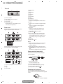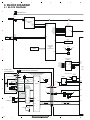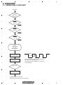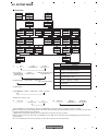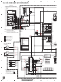
1
ORDER NO.
CRT4632
DEH-2350UB/XNES
CD RDS RECEIVER
DEH-2350UB
/XNES
DEH-2350UBG
DEH-2350UBSW
DEH-2350UB
DEH-2350UB
/XNES
/XNES
/XSES
/XNES1
This service manual should be used together with the following manual(s):
Model No.
CX-3269
Order No.
CRT4488
Mech. Module
S11.1STD-DOUT
Remarks
CD Mech. Module : Circuit Descriptions, Mech. Descriptions, Disassembly
For details, refer to "Important Check Points for Good Servicing".
PIONEER CORPORATION
1-1, Shin-ogura, Saiwai-ku, Kawasaki-shi, Kanagawa 212-0031, Japan
PIONEER ELECTRONICS (USA) INC. P.O. Box 1760, Long Beach, CA 90801-1760, U.S.A.
PIONEER EUROPE NV Haven 1087, Keetberglaan 1, 9120 Melsele, Belgium
PIONEER ELECTRONICS ASIACENTRE PTE. LTD. 253 Alexandra Road, #04-01, Singapore 159936
PIONEER CORPORATION 2010
K-ZZZ OCT. 2010 Printed in Japan
1
2
3
4
SAFETY INFORMATION
This service manual is intended for qualified service technicians; it is not meant for the casual do-it-yourselfer.
Qualified technicians have the necessary test equipment and tools, and have been trained to properly and safely repair
complex products such as those covered by this manual.
Improperly performed repairs can adversely affect the safety and reliability of the product and may void the warranty.
If you are not qualified to perform the repair of this product properly and safely, you should not risk trying to do so
and refer the repair to a qualified service technician.
A
Where in a manufacturer’s service documentation, for example in circuit diagrams or lists
of components, a symbol is used to indicate that a specific component shall be replaced only
by the component specified in that documentation for safety reasons, the following symbol shall
be used:
B
- Safety Precautions for those who Service this Unit.
When checking or adjusting the emitting power of the laser diode exercise caution in order to get safe, reliable
results.
Caution:
1. During repair or tests, minimum distance of 13 cm from the focus lens must be kept.
2. During repair or tests, do not view laser beam for 10 seconds or longer.
CAUTION:
USE OF CONTROLS OR ADJUSTMENTS OR PERFORMANCE OF PROCEDURES OTHER THAN THOSE
SPECIFIED HEREIN MAY RESULT IN HAZARDOUS RADIATION EXPOSURE.
C
CAUTION
This product is a class 1 laser product classified under the Safety of laser products, IEC
60825-1:2007, and contains a class 1M laser
module. To ensure continued safety, do not remove any covers or attempt to gain access to
the inside of the product. Refer all servicing to
qualified personnel.
D
CAUTION—CLASS 1M INVISIBLE LASER
RADIATION WHEN OPEN, DO NOT VIEW
DIRECTLY WITH OPTICAL INSTRUMENTS.
WARNING!
The AEL (accessible emission level )of the laser power output is less than CLASS 1
but the laser component is capable of emitting radiation exceeding the limit for
CLASS 1.
A specially instructed person should do servicing operation of the apparatus.
E
Laser diode characteristics
Wave length : 785 nm to 814 nm
Maximum output : 1 190 µW(Emitting period : unlimited)
Additional Laser Caution
Transistors Q101 in PCB drive the laser diodes.
When Q101 is shorted between their terminals, the laser diodes will radiate beam.
If the top cover is removed with no disc loaded while such short-circuit is continued,
the naked eyes may be exposed to the laser beam.
F
2
DEH-2350UB/XNES
1
2
3
4
5
6
7
8
CAUTION
Danger of explosion if battery is incorrectly replaced.
Replaced only with the same or equivalent type recommended by the manufacture.
Discord used batteries according to the manufacture's instructions.
A
B
C
D
E
F
DEH-2350UB/XNES
5
6
7
8
3
1
2
3
4
[Important Check Points for Good Servicing]
A
In this manual, procedures that must be performed during repairs are marked with the below symbol.
Please be sure to confirm and follow these procedures.
1. Product safety
Please conform to product regulations (such as safety and radiation regulations), and maintain a safe servicing environment by
following the safety instructions described in this manual.
1 Use specified parts for repair.
Use genuine parts. Be sure to use important parts for safety.
2 Do not perform modifications without proper instructions.
Please follow the specified safety methods when modification(addition/change of parts) is required due to interferences such as
radio/TV interference and foreign noise.
B
3 Make sure the soldering of repaired locations is properly performed.
When you solder while repairing, please be sure that there are no cold solder and other debris.
Soldering should be finished with the proper quantity. (Refer to the example)
4 Make sure the screws are tightly fastened.
Please be sure that all screws are fastened, and that there are no loose screws.
5 Make sure each connectors are correctly inserted.
Please be sure that all connectors are inserted, and that there are no imperfect insertion.
6 Make sure the wiring cables are set to their original state.
C
Please replace the wiring and cables to the original state after repairs.
In addition, be sure that there are no pinched wires, etc.
7 Make sure screws and soldering scraps do not remain inside the product.
Please check that neither solder debris nor screws remain inside the product.
8 There should be no semi-broken wires, scratches, melting, etc. on the coating of the power cord.
Damaged power cords may lead to fire accidents, so please be sure that there are no damages.
If you find a damaged power cord, please exchange it with a suitable one.
9 There should be no spark traces or similar marks on the power plug.
When spark traces or similar marks are found on the power supply plug, please check the connection and advise on secure
connections and suitable usage. Please exchange the power cord if necessary.
D
a Safe environment should be secured during servicing.
When you perform repairs, please pay attention to static electricity, furniture, household articles, etc. in order to prevent injuries.
Please pay attention to your surroundings and repair safely.
2. Adjustments
To keep the original performance of the products, optimum adjustments and confirmation of characteristics within specification.
Adjustments should be performed in accordance with the procedures/instructions described in this manual.
3. Lubricants, Glues, and Replacement parts
E
Use grease and adhesives that are equal to the specified substance.
Make sure the proper amount is applied.
4. Cleaning
For parts that require cleaning, such as optical pickups, tape deck heads, lenses and mirrors used in projection monitors, proper
cleaning should be performed to restore their performances.
5. Shipping mode and Shipping screws
To protect products from damages or failures during transit, the shipping mode should be set or the shipping screws should be
installed before shipment. Please be sure to follow this method especially if it is specified in this manual.
F
4
DEH-2350UB/XNES
1
2
3
4
5
6
7
8
CONTENTS
SAFETY INFORMATION .....................................................................................................................................2
1. SERVICE PRECAUTIONS................................................................................................................................6
1.1 SERVICE PRECAUTIONS .........................................................................................................................6
1.2 NOTES ON SOLDERING ...........................................................................................................................7
2. SPECIFICATIONS.............................................................................................................................................8
2.1 SPECIFICATIONS ......................................................................................................................................8
2.2 DISC/CONTENT FORMAT .........................................................................................................................8
2.3 PANEL FACILITIES.....................................................................................................................................9
2.4 CONNECTION DIAGRAM........................................................................................................................10
3. BASIC ITEMS FOR SERVICE ........................................................................................................................11
3.1 CHECK POINTS AFTER SERVICING .....................................................................................................11
3.2 PCB LOCATIONS .....................................................................................................................................12
3.3 JIGS LIST .................................................................................................................................................13
3.4 CLEANING ...............................................................................................................................................13
4. BLOCK DIAGRAM ..........................................................................................................................................14
4.1 BLOCK DIAGRAM....................................................................................................................................14
5. DIAGNOSIS ....................................................................................................................................................16
5.1 OPERATIONAL FLOWCHART .................................................................................................................16
5.2 ERROR CODE LIST.................................................................................................................................17
5.3 CONNECTOR FUNCTION DESCRIPTION .............................................................................................19
6. SERVICE MODE.............................................................................................................................................20
6.1 DISPLAY TEST MODE .............................................................................................................................20
6.2 CD TEST MODE.......................................................................................................................................21
7. DISASSEMBLY ...............................................................................................................................................22
8. EACH SETTING AND ADJUSTMENT ............................................................................................................28
8.1 CD ADJUSTMENT ...................................................................................................................................28
8.2 CHECKING THE GRATING AFTER CHANGING THE PICKUP UNIT ....................................................29
8.3 PCL OUTPUT CONFIRMATION...............................................................................................................31
9. EXPLODED VIEWS AND PARTS LIST ..........................................................................................................32
9.1 PACKING ..................................................................................................................................................32
9.2 EXTERIOR ...............................................................................................................................................34
9.3 CD MECHANISM MODULE .....................................................................................................................36
10. SCHEMATIC DIAGRAM................................................................................................................................38
10.1 TUNER AMP UNIT (GUIDE PAGE) ........................................................................................................38
10.2 KEYBOARD UNIT ..................................................................................................................................44
10.3 CD CORE UNIT (S11.1STD-DOUT) ......................................................................................................46
10.4 WAVEFORMS.........................................................................................................................................48
11. PCB CONNECTION DIAGRAM ....................................................................................................................50
11.1 TUNER AMP UNIT .................................................................................................................................50
11.2 KEYBOARD UNIT ..................................................................................................................................54
11.3 CD CORE UNIT (S11.1STD-DOUT) ......................................................................................................56
12. ELECTRICAL PARTS LIST ...........................................................................................................................58
A
B
C
D
E
F
DEH-2350UB/XNES
5
6
7
8
5
1
2
3
4
1. SERVICE PRECAUTIONS
1.1 SERVICE PRECAUTIONS
A
1. You should conform to the regulations governing the product (safety, radio and noise, and other
regulations), and should keep the safety during servicing by following the safety instructions
described in this manual.
2. Before disassembling the unit, be sure to turn off the power. Unplugging and plugging the connectors
during power-on mode may damage the ICs inside the unit.
3. To protect the pickup unit from electrostatic discharge during servicing, take an appropriate treatment
(shorting-solder) by referring to "the DISASSEMBLY".
4. After replacing the pickup unit, be sure to check the grating.
5. Be careful in handling ICs. Some ICs such as MOS type are so fragile that they can be damaged by
electrostatic induction.
6.
area and a heat sink becomes hot areas. Be careful not to burn yourself.
B
C
D
7. Software update
The software of this product is stored in IC671.
Please replace IC671 when making the version upgrade of software.
8. How to Handle Infrared Deteching unit for Remote Control of Grille
The infrared deteching unit for remote control of keyboard unit is not fixed with cushion, etc.
When external force is applied on the infrared deteching unit for remote control, the light receiving sensitivity might be
deteriorated since the lead bents and attaching angle of the light receiving part may be varied.
Please do not apply external force onto the infrared deteching unit for remote control. If any external force is applied by
mistake, please confirm whether lead bending may exist or not.
If the lead is bent, please correct the angle between the lead and the light receiving part to be 90 degrees or replace
the infrared deteching unit for remote control (GP1UXC14RK).
E
F
6
DEH-2350UB/XNES
1
2
3
4
5
6
7
8
9. Capacitor Bond Lock
Silicon Glue (GEM1017)
Place the capacitor in the center of the silk print, and confirm it does not touch to the connector. Then, apply silicon glue.
A
NG
OK
B
C
D
1.2 NOTES ON SOLDERING
For environmental protection, lead-free solder is used on the printed circuit boards mounted in this unit.
Be sure to use lead-free solder and a soldering iron that can meet specifications for use with lead-free solders for repairs
accompanied by reworking of soldering.
Compared with conventional eutectic solders, lead-free solders have higher melting points, by approximately 40 C.
Therefore, for lead-free soldering, the tip temperature of a soldering iron must be set to around 373 C in general, although
the temperature depends on the heat capacity of the PC board on which reworking is required and the weight of the tip of
the soldering iron.
E
Compared with eutectic solders, lead-free solders have higher bond strengths but slower wetting times and higher melting
temperatures (hard to melt/easy to harden).
The following lead-free solders are available as service parts:
Parts numbers of lead-free solder:
GYP1006 1.0 in dia.
GYP1007 0.6 in dia.
GYP1008 0.3 in dia.
F
DEH-2350UB/XNES
5
6
7
8
7
1
2
3
4
2. SPECIFICATIONS
2.1 SPECIFICATIONS
A
B
C
General
USB
Rated power source...............14.4 V DC
(allowable voltage range:
12.0 V to 14.4 V DC)
Grounding system...................Negative type
Maximum current consumption
.....................................................10.0 A
Backup current .......................4.0 mA or less
Dimensions (W × H × D):
DIN
Chassis .....................178 mm × 50 mm × 165
mm
Nose ...........................188 mm × 58 mm × 17 mm
D
Chassis .....................178 mm × 50 mm × 165
mm
Nose ...........................170 mm × 46 mm × 17 mm
Weight ..........................................1.2 kg
USB standard specification
.....................................................USB 2.0 full speed
Maximum current supply .... 500 mA
USB Class...................................MSC (Mass Storage Class)
File system..................................FAT12, FAT16, FAT32
WMA decoding format .........Ver. 7, 7.1, 8, 9, 10, 11, 12
(2ch audio)
(Windows Media Player)
MP3 decoding format ...........MPEG-1 & 2 Audio Layer 3
WAV signal format ..................Linear PCM & MS ADPCM
(Non-compressed)
Audio
AM tuner
Maximum power output .......50 W × 4
Continuous power output ... 22 W × 4 (50 Hz to 15 000
Hz, 5 % THD, 4 load, both
channels driven)
Load impedance ......................4 (4 to 8 allowable)
Preout maximum output level
.....................................................2.0 V
Tone controls:
Bass
Frequency................100 Hz
Gain ............................±12 dB
Mid
Frequency................1 kHz
Gain ............................±12 dB
Treble
Frequency................10 kHz
Gain ............................±12 dB
Subwoofer (mono):
Frequency..........................50/63/80/100/125 Hz
Slope....................................–18 dB/oct
Gain ......................................+6 dB to –24 dB
Phase ..................................Normal/Reverse
Frequency range......................531 kHz to 1 602 kHz (9 kHz)
530 kHz to 1 640 kHz (10
kHz)
Usable sensitivity.....................25 µV (S/N: 20 dB)
Signal-to-noise ratio...............62 dB (IEC-A network)
CD player
D
System ..........................................Compact disc audio system
Usable discs ..............................Compact disc
Signal-to-noise ratio...............94 dB (1 kHz) (IEC-A network)
Number of channels ..............2 (stereo)
WMA decoding format .........Ver. 7, 7.1, 8, 9, 10, 11, 12
(2ch audio)
(Windows Media Player)
MP3 decoding format ...........MPEG-1 & 2 Audio Layer 3
WAV signal format ..................Linear PCM & MS ADPCM
(Non-compressed)
FM tuner
Frequency range......................87.5 MHz to 108.0 MHz
Usable sensitivity.....................9 dBf (0.8 µV/75 , mono,
S/N: 30 dB)
Signal-to-noise ratio...............72 dB (IEC-A network)
SW tuner (DEH-2350UBSW)
Frequency range......................2 300 kHz to 7 735 kHz
(2 300 kHz to 2 495 kHz, 2
940 kHz to 4 215 kHz, 4 540
kHz to 5 175 kHz, 5 820 kHz
to 6 455 kHz, 7 100 kHz to 7
735 kHz)
9 500 kHz to 21 975 kHz
(9 500 kHz to 10 135 kHz, 11
580 kHz to 12 215 kHz, 13
570 kHz to 13 870 kHz, 15
100 kHz to 15 735 kHz, 17
500 kHz to 17 985 kHz, 18
015 kHz to 18 135 kHz, 21
340 kHz to 21 975 kHz)
Usable sensitivity.....................28 µV (S/N: 20 dB)
Signal-to-noise ratio...............62 dB (IEC-A network)
Infrared remote control
Wavelength.................................940 nm ±50 nm
Output ...........................................typ; 12 mw/sr per Infrared
LED
Note
Specifications and the design are subject to modifications without notice.
E
2.2 DISC/CONTENT FORMAT
F
8
DEH-2350UB/XNES
1
2
3
4
5
6
7
8
2.3 PANEL FACILITIES
A
Head unit
12 3 4
5
7 8 9
1
6
a
b
P art
S (SRC/OFF)
(Back/display/
scroll)
2
(eject)
9
3
(list)
a
FUNCTION
Press to select functions.
Press and hold to recall the initial
setting menu when the sources
are off.
k
LIST/
ENTER
Press to display the disc title,
track title, folder, or file list depending on the source.
While in the operating menu,
press to control functions.
c d
P art
8
j
B
Display indication
/DISP OFF
4
MULTI-CONTROL
(M.C.)
b
1 to 6
5
Disc loading slot
c
AUX input jack (3.5
mm stereo jack)
6
USB port
d
Detach button
7
B (BAND/ESC)
1
23 6 8
45 7
CAUTION
Indicator
Use an optional Pioneer USB cable (CD-U50E)
to connect the USB audio player/USB memory as any device connected directly to the
unit will protrude out from the unit and may
be dangerous.
Do not use unauthorized products.
1
Remote control
f
9
g
7
k
j
3
A lower tier of folder or menu exists.
(list)
The list function is operated.
5
(artist)
The disc (track) artist name is displayed.
6
(disc)
The disc (album) name is displayed.
7
(song)
The track (song) name is displayed.
A playable audio file has been selected while operating the list.
8
Part
Operation
a
VOLUME
Press to increase or decrease volume.
b
f
MUTE
Press to mute. Press again to unmute.
g
AUDIO
Press to select an audio function.
h
Press to select different displays.
DISP/SCRL Press and hold to scroll through
the text information.
LOC
(repeat)
(random)
(sound retriever)
C
Tuner: band and frequency
Program service name
Built-in CD player and USB:
elapsed playback time and
text information
An upper tier of folder or menu
exists.
9
e
b
State
Main display section
h
1
i
a
2
4
e
9
D
The local seek tuning is on.
Track or folder repeat is on.
E
Random play is on.
The sound retriever function is
on.
Press to pause or resume playback.
i
F
DEH-2350UB/XNES
5
6
7
8
9
1
2
3
4
2.4 CONNECTION DIAGRAM
A
This unit
3
1
2
3
4
5
B
5
6
7
8
9
a
b
c
d
e
2
1
4
5
Power cord input
Rear output or subwoofer output
Antenna input
Fuse (10 A)
Wired remote input
Hard-wired remote control adaptor can be
connected (sold separately).
f
g
Power cord
h
Perform these connections when not connecting a rear speaker lead to a subwoofer.
1
L
4
C
F
5
R
i
j
R
2
3
6
7
8
9
a
b
c
d
k
l
e
f
g
h
Perform these connections when using a subwoofer without the optional amplifier.
D
1
L
R
2
4
F
i
SW
Rear speaker
White
White/black
Gray
Gray/black
Green
Green/black
Violet
Violet/black
Black (chassis ground)
Connect to a clean, paint-free metal location.
Yellow
Connect to the constant 12 V supply terminal.
Red
Connect to terminal controlled by ignition
switch (12 V DC).
Blue/white
Connect to system control terminal of the
power amp or auto-antenna relay control
terminal (max. 300 mA 12 V DC).
Subwoofer (4 )
When using a subwoofer of 70 W (2 ), be
sure to connect the subwoofer to the violet
and violet/black leads of this unit. Do not connect anything to the green and green/black
leads.
Not used.
Subwoofer (4 )× 2
Notes
With a 2 speaker system, do not connect anything to the speaker leads that are not connected to speakers.
Change the initial setting of this unit. Refer to
SW CONTROL (rear output and subwoofer setting).
The subwoofer output of this unit is monaural.
3
6
7
8
9
a
b
c
d
Power amp (sold separately)
Perform these connections when using the
optional amplifier.
3
1
2
4
e
f
g
h
E
1
2
3
4
j
5
a
c
b
d
k
l
5
1 System remote control
Connect to Blue/white cable.
2 Power amp (sold separately)
3 Connect with RCA cable (sold separately)
4 To Rear output or subwoofer output
5 Rear speaker or subwoofer
To power cord input
Left
Right
Front speaker
Fastening the front panel
If you do not plan to detach the front panel,
the front panel can be fastened with the supplied
screw.
F
Screw
ES, ES1 : XXX7020
10
DEH-2350UB/XNES
1
2
3
4
5
6
7
8
3. BASIC ITEMS FOR SERVICE
3.1 CHECK POINTS AFTER SERVICING
A
To keep the product quality after servicing, please confirm following check points.
No.
1
4
Procedures
Confirm whether the customer complain has
been solved.
If the customer complain occurs with the
specific media, use it for the operation check.
Play back a CD.
(Track search)
Check FM/AM tuner action.
(Seek, Preset)
Switch band to check both FM and AM.
Check whether no disc is inside the product.
5
Appearance check
2 CD
3 FM/AM tuner
Item to be confirmed
The customer complain must not be
reappeared.
Display, audio and operations must be
normal.
No malfunction on display, audio and
operation.
Display, audio and operations must be
normal.
B
The media used for the operating check must
be ejected.
No scratches or dirt on its appearance after
receiving it for service.
See the table below for the items to be checked regarding audio:
Item to be checked regarding audio
Distortion
Noise
Volume too low
Volume too high
Volume fluctuating
Sound interrupted
C
D
E
F
DEH-2350UB/XNES
5
6
7
8
11
1
2
3
4
3.2 PCB LOCATIONS
A
C CD Core Unit (S11.1STD-DOUT)
B
A Tuner Amp Unit
C
B Keyboard Unit
A:DEH-2350UB/XNES
B:DEH-2350UBG/XNES
D
C:DEH-2350UBSW/XNES
D:DEH-2350UB/XSES
E:DEH-2350UB/XNES1
Unit Number
: CWN5489 (A, B, D, E)
: CWN5479 (C)
E
Unit Name
: Tuner Amp Unit
Unit Number
:
Unit Name
: Keyboard Unit
Unit Number
: CWX3985
Unit Name
: CD Core Unit (S11.1STD-DOUT)
F
12
DEH-2350UB/XNES
1
2
3
4
5
6
7
8
3.3 JIGS LIST
- Jigs List
Name
16P FFC
Test Disc
L.P.F.
A
Jig No.
GGD1310
TCD-782
Remarks
Tuner Amp Unit - CD Core Unit
Checking the grating
Checking the grating (Two pieces)
Grease No.
GEM1024
GEM1038
GEM1043
GEM1045
GEM1017
Remarks
CD Mechanism Module
CD Mechanism Module
CD Mechanism Module
CD Mechanism Module
Capacitor Bond Lock
- Grease List
Name
Grease
Grease
Grease
Grease
Silicon Glue
B
3.4 CLEANING
C
Before shipping out the product, be sure to clean the
following portions by using the prescribed cleaning
tools:
Portions to be cleaned
CD pickup lenses
Cleaning tools
Cleaning liquid : GEM1004
Cleaning paper : GED-008
D
E
F
DEH-2350UB/XNES
5
6
7
8
13
1
2
3
4
4. BLOCK DIAGRAM
4.1 BLOCK DIAGRAM
A
A
TUNER AMP UNIT
JA401
5
1
ANTENNA
16
2,3
18
FMMIXIN1
57
DACOUTL
PINDIN
LNAIN
RF FRONT END IC
IC401
TDA7706
34
I2CSCL
I2CSDA
RSTN
33
112 TUNSCL
111
TUNSDA
31
107
DAC
IC231
PCM1753DBQ
TUNPCE1
DACSCK
DACDATA
DACBDATA
B
DACBSCK
AUDIO_XOUT
DACLRCK
DACCS
1
91
BCK
88
2
87
13
DATA
85
14
84
16
89
3
124
15
MD
VOUTL
MC
7
SCK
LRCK
ML
JA961
WIRED
REMOTE
2 KEYAD
69
3 KEYD
129
KEYAD
KEYD
1 GND
RESET
38
RES
SYSTEM MICRO
COMPUTER
IC601
(1/2)
R5S7266ZD144FP
FLASH ROM
IC671
PEA011A8
IC651
S-80827CNMC-B8M
1
ILMPW
Q873
B.UP
ILM+B
C
Q872
ILMPW
132
REGULATOR IC
IC912
BA49182-V12
6
SW5V
SW5V
9
SWVDD
SYS+B
7
C
PICKUP UNIT
(P10.5)(SERVICE)
SYSPW
2
3
+B
VDD12
LD
LD-
MD
15
MD 5
12
15
5
8
8
V+3A
VDD
RF AMP, CD DECODER, MP3&WMA DECODER
DIGITAL SERVO/DATA • PROCESSOR
CPU, USB HOST CONTROLLER
GND
1
Q101
2
PD
93
REFO
USB5V REGULATOR
IC501
BD2226G
LD
Q102
PD
V+3A
VIN
VDD
FOCUS ACT.
TRACKING ACT.
E
FOP
3
2
TOP 1
TOM 4
LD+
14
3
2
FOM
FOP
USB5V
EN
5 VOUT
OC
1
B.UP
8
1
2
4 TOM
TD,FD
SD,MD
CN701
PVIN
VIN
EN/ 5
SYNC
19
VDD
3
18
4
20
CN701
9
8
VDD
SYNC
SW
USBCTL
USBFLG
VBUS
VDD3.3V
VD
VD
VO1-
VDSENS
2
15
1
16
VD
Q751
B.UP
Q752
VO2+
VO2-
M
15
VO3+
16
VO3-
M
LCOM
LCOP
17
VO4+
18
VO4-
14
LDIN
CNT
22
41
21
40
39
MUTE 9
38
35
S903
DSCSNS
67
MECHA VD
VO1+
SOM
SOP
CLCONT
CONT
RESET
29
RESET
8
CD DATA (CDSRQ,CDSTBY,SKIP,
SCL,SDA,DATA,BCLK,LRCK,WAIT)
9
RESET
120
CD DATA (CDSRQ,CDSTBY,SKIP,
SCL,SDA,DATA,BCLK,LRCK,WAIT)
DSCSNS
HOME
S901
HOME
2
VDCONT
LOEJ
DEH-2350UB/XNES
1
IC502
BD9008F
54
VDD
14 LD+
13
14
SYST
CO
IC301
BA5839FP
1 TOP
14
F
54
ACTUATOR/
MOTOR DRIVER
11
LOADING/CARRIAGE
MOTOR
PUEN
IC201
PE5756A
12
SPINDLE
MOTOR
REFOUT
AC,BD,E,F
HOLOGRAM
UNIT
FOM
B.UP
R5S72
REFO
VREF
4
10
CD CORE UNIT(S11.1 STD-DOUT)
CN101
12
VCC
128 SWVDD
141
BSENS
7 SYSPW
1
SW5VCNT
+BUP
D
11
VDD
8
VDD1.2V
BSENS
SWVDD
5
SYS+B
VDD3.3V
VDDCONT
3
4
CDRST
5
6
7
8
A
JA251
PL
3
PRE OUT
Q251
RCAG
TUNL
2
CD_Lch
1
P251
ELECTRONIC VOLUME/
SOURCE SELECTOR
IC201
PML022A
1
POUT_L 6
IN2_L
IN1_L
B
JA901
FUSE 10 A
AUX_Lch
4
B.UP
IN4+_L
FRONT_L
VST
VCK
VDT
26
15
30
14
31
13
18
STB
REAR_L
7
11
8
12
FL+
FLIn
RLIn
CLK
FL- 7
FL-
5
RL+
3
RL-
RL+
AMP
IC301
PAL007E
DATA
17
B.UP 15
FL+ 1
9
RL-
3
5
7
MUTE
Q351
(1/2)
22
BREM
B.REM 25
MUTE
14
POWER
CONNECTOR
Q351
(2/2)
MUTE
C
21
ASENS
Q931
ASENS
143
ACC
128 SWVDD
141
BSENS
7 SYSPW
B.UP
B
SYSTEM MICRO
COMPUTER
IC601
(2/2)
R5S7266ZD144FP
13
KEYBOARD UNIT
CN1901
CN801
SSENS
AUX L
19
SOURCE
18
142
19
18
FRONT_AUX
AUXGND 1
AUXR 3
AUXL 2
CN1821
AUXL
SOURCE
D
SOURCE 4
S1841
ROTARY COMMANDER
02
008F
S1845
ROT0
EN/ 5
SYNC
19
ROT1
131
ROT0
130
ROT1
6
4
6
4
ROT0
2
5
KDT2
ROT1
1
4
KST1
SYNC
3
18
20
USBCTL
KDT0
USBFLG
KDT1
KST2_2
54
KDT3
VBUS
KST0
KST1
KYDT
67
29
KYDT
8
8
20
KYDT
KST2_1
KYDT
IC801
TC7SET08FUS1
VDSENS
DPDT
28
2
4
DPDT
10
10
20
20
DPDT
18
DPDT
LCD DRIVER/
KEY CONTROLLER
IC1801
PD6340A
KST3
KST4
15
16
25
26
14
KEY MATRIX
13
12
11
28
E
LCD
V1801
B.UP
DSENS
14
120
DSENS
140
DSENS
VDCONT
REM
ILM+B
CDRST
5
5
3
3
17
1
REMOTE CONTROL
SENSOR
IC1802
GP1UXC14RK
ILM+B
D1868,D1869,D1870,D1871,
SWVDD
SW5V
SW5V
D1872,D1873,D1874,D1875,
D1876,D1877,D1878,D1879,
D1913
D1880,D1881,D1882,D1883
F
CN1911
USB5V
DM
DP
52
DM
53
DP
11
11
13
13
15
15
USB5V
USB5V
DM
DM
DP
DP
DEH-2350UB/XNES
5
6
7
8
2
3
USB
4
15
1
2
3
4
5. DIAGNOSIS
5.1 OPERATIONAL FLOWCHART
A
Power ON
Vcc = 1.2 V
Pin 5
PVcc = 3.3 V
Pin 1
BSENS
B
Pin 141
BSENS = L
ASENS
Pin 143
ASENS = L
C
DSENS
Pin 140
DSENS = L
Starts
communication
with Grille
microcomputer.
D
300 ms
SWVDD <- H
Pin 128
300 ms
In case of the above signal, the communication
with Grille microcomputer may fail.
If the time interval is not 300 msec, the oscillator
may be defective.
Source keys
operative
E
Source ON
SYSPW <- H
Pin 7
F
Completes power-on operation.
(After that, proceed to each source operation)
16
DEH-2350UB/XNES
1
2
3
4
5
6
7
8
5.2 ERROR CODE LIST
ERROR CODES
A
If a CD memory device is inoperable, or operation of such media is stopped by an error, the error mode is established and a
cause of the error is displayed by an error code. Indication of error codes is intended to reduce the number of calls from
customers and facilitate failure analysis and repair work in servicing.
(1) DISPLAY METHOD
If “0xFD” error mode is displayed in CD MODE (CD MODE area for display), an error code will be displayed in the MIN (minute
display) and SEC (second display) areas.
The same code is displayed in the MIN and SEC areas.
The TNO area is blank (#0FFH), as it conventionally was.
• Display example of the main unit
Depending on the display capability of LCDs, the display format varies, as shown below. XX denotes an error number.
Note: In a case of an OEM product, the error display format is subject to the specifications used by the equipment
manufacturer.
8-digit display
6-digit display
ERROR-xx
ERR-xx
B
4-digit display
E-xx
(2) LIST OF CD ERROR CODES (Error Mode: 0xFD)
Code Classification Error code to be displayed
Details and possible causes
C
7
Servo
TOC reading NG
TOC information cannot be read.
--> The partial disk or TOC content is illegal.
10
Servo
Carriage Home NG
11
Servo
Focus Search NG
The CRG cannot move toward the inner track.
The CRG cannot move from the inner track.
--> Defective HOME SW; Failure in CRG movement.
Focusing not available
--> Disc placed upside-down; Stains on the disc; excessive vibration.
12
Servo
Spindle Lock NG
Subcode NG
RF-amp NG
Spindle not locked. Subcode not readable.
Proper RF AMP gain not obtained.
--> Defective spindle; Scratches or stains on the disc; excessive vibration.
--> A CD-R disc that does not contain data loaded, or in a rare case, disc placed upside-down.
--> CD signal error.
15
Servo
Failure in RF data
RF not read
--> A CD-R disc that does not contain data loaded
--> A CD-RW disc that does not contain data loaded
17
Servo
Setup NG
AGC protection does not work. Focus can be easily lost.
--> Scratches or stains on the disc; excessive vibration.
30
Servo
Search Time Out
Failed to reach a target address
--> CRG tracking error; Scratches on the disc; Stains on the disc
50
Mechanism
Failure in ejection
Load NG
Disc ejection not completed
Disc loading not completed
--> A foreign object inserted in the mechanism; Disc jammed.
51
Mechanism
Failure in retried
turning for ejection
Disc could not be ejected even after disc turning had been retried.
--> A foreign object inserted in the mechanism; Disc jammed.
D
E
NOTES
• Indications of error codes are available only during disc operations, because CD operations are
unavailable if a mechanical error is generated.
• If the TOC cannot be read, this is not processed as an error, and operation continues accordingly.
• If you design a new head unit, be sure to use one of the display formats indicated in “Display example of
the main unit.”
• The 2 high-order digits of an error code denote the main
• How to restore from each error is shown below.
classification, shown below.
0x, 1x and 3x: ACC-OFF then ON, CD-OFF then ON,
0x: Servo-related errors
Disc ejection
1x: Servo-related errors
5X: ACC-OFF then ON, Disc ejection, Disc reloading
3x: Servo-related errors
5x: Mechanism-related errors
DEH-2350UB/XNES
5
6
7
8
F
17
1
2
3
4
USB storage device
A
Message
Cause
NO DEVICE
Turn the plug
When plug and
and play on.
play is off, no
USB storage deConnect a compatible USB stovice is conrage device.
nected.
FRMT READ
Sometimes there
is a delay between the start of
playback and
when you start to
hear any sound.
NO AUDIO
Action
Transfer the audio
files to the USB
storage device and
connect.
The connected
USB storage device has security
enabled
Follow the USB
storage device instructions to disable the security.
SKIPPED
The connected
USB storage device contains
WMA files embedded with
Windows Media DRM 9/10
Play an audio file
not embedded with
Windows Media
DRM 9/10.
PROTECT
All the files in the
USB storage device are embedded with
Windows Media
DRM 9/10
Transfer audio files
not embedded with
Windows Media
DRM 9/10 to the
USB storage device and connect.
N/A USB
Connect a USB
The USB device
connected to is portable audio
not supported by player or USB
memory that is
this unit.
USB Mass Storage
Class compliant.
Disconnect your
device and replace
it with a compatible USB storage
device.
CHECK USB
The USB connec- Check that the
tor or USB cable USB connector or
USB cable is not
has shortcaught in somecircuited.
thing or damaged.
C
D
The connected
USB portable
audio player/
USB memory
consumes more
than maximum
allowable current.
E
Cause
Action
Communication
failed.
Perform one of the
following operations.
–Turn the ignition
switch OFF and
back ON.
–Disconnect the
USB portable
audio player/USB
memory.
–Change to a different source.
Then, return to the
USB portable
audio player/USB
memory.
ERROR-23
USB storage device is not formatted with
FAT12, FAT16 or
FAT32
USB storage device should be formatted with FAT12,
FAT16 or FAT32.
Wait until the message disappears
and you hear
sound.
There are no
songs.
B
Message
ERROR-19
Disconnect the
USB portable
audio player/USB
memory and do
not use it. Turn the
ignition switch to
OFF, then to ACC
or ON and then
connect a compliant USB portable
audio player/USB
memory.
F
18
DEH-2350UB/XNES
1
2
3
4
5
6
7
8
5.3 CONNECTOR FUNCTION DESCRIPTION
A
B
WIRED
REAR
REMOTE OUTPUT
CONTROL
ANTENNA
15 13 11 9 7 5 3 1
16 14 12 10 8 6 4 2
1
2
3
4
5
6
7
8
9
10
11
12
13
14
15
16
FL+
FR+
FLFRRL+
RR+
RLRR-
NC
NC
NC
NC
ACC
B.REM
B.UP
GND
C
D
E
F
DEH-2350UB/XNES
5
6
7
8
19
1
2
3
4
6. SERVICE MODE
6.1 DISPLAY TEST MODE
A
The information such as the system microcomputer version is checked.
[How to enter Test mode]
Press “ 1 ” and “ 3 ” keys simultaneously to start resetting.
[Operation key]
Operation key
Processing
Remarks
Enter display test mode (2)
Switch to next test mode
1+3
B
[Test items]
Start display test mode (2).
(Press “ 1 ” + “ 3 ” keys simultaneously to start resetting.)
Key Illumination
Icon
Off
All off
On (an initial value)
All off
* Initial
condition
C
S
$ $ $ $
# # #
$ PD number
For PEA010A, "010A" is displayed
# System
microcomputer
version
For Ver.7.01, "701" is displayed
On (an initial value or
setting value of default
menu)
All off
D
Switching to next display
by pressing “ 1 ” + “ 3 ” keys simultaneously.
Display is normally updated
Product operation is performed as usual, in appearance. On (an initial value or
setting value of default
Switching to next display
menu)
by pressing “ 1 ” + “ 3 ” keys simultaneously.
E
On (lighting condition
of normal times)
Display update is stopped
The screen gets still when entering this item.
Switching to next display
by pressing “ 1 ” + “ 3 ” keys simultaneously.
On (an initial value or
setting value of default
menu)
On (state when
entering test mode)
F
20
DEH-2350UB/XNES
1
2
3
4
5
6
7
8
6.2 CD TEST MODE
- Flow Chart
Test Mode IN
TRK
Contents
MIN
Display
[BAND]
[2]
RF AMP *1
Gain switching
TRK MIN SEC
Power On
(T.Offset is adjusted)
TRK MIN SEC
00
[BAND]
TRK
MIN
00
SEC
[BAND]
91
91
SEC
TRK
MIN
TRK
MIN
SEC
0X
0X
0X
TRK
MIN
SEC
[<]
00 00 00
or 99 99 99
[3]
??
??
??
[3]
F,T,RF AGC*7
F.Bias display switching
TRK MIN SEC
??
??
??
[>]
[2]
CRG +
CRG -
*8
00 00 00
or 99 99 99
*8
00 00 00
or 99 99 99
[<]
RF AGC /
RF AGC coefficient display
TRK MIN SEC
SEC
[1]
Power Off
GG
Tracking Servo
Close
*2
?tr ?min ?sec
[BAND]
GG
[1]
Focus Mode switching
[1]
T.Close & AGC
Applicable servomechanism
Power Off
MIN
GG
[6]
Focus Close
S curve check
TRK MIN SEC
91
TRK
00
[3]
Power Off
A
[Key]
[CD] or [SOURCE]
Source ON
[4] + [6] -> BUP + ACC ON
Self-adjusting
switching *3
MIN SEC
TRK
??
[>]
CRG -
8X 8X 8X
or 9X 9X 9X
8X 8X 8X
or 9X 9X 9X
[<]
[>]
CRG/TR Jump -
*4
*4
?tr ?min ?sec
?tr ?min ?sec
MIN
SEC
T.Balance adjustment /
T.BAL coefficient display
TRK MIN SEC
??
??
??
[2]
CRG/TR Jump +
TRK
B
??
[2]
CRG +
F,T AGC / F.Bias
RF AGC
TRK MIN SEC
??
TRK
MIN
Tracking Open
SEC
?tr ?min ?sec
8X 8X 8X
or 9X 9X 9X
*6
C
[BAND]
[2]
Power Off
TRK
*1)
MIN
Tracking Open
t
TYP
TRK
8X 8X 8X
or 9X 9X 9X
SEC
MIN
SEC
*2) Focus Close
t
TRK
00MIN00SEC00
(TRK99MIN99SEC99)
+ 6 dB
t
TRK
06MIN06SEC06
S. Curve
t
01MIN01SEC01
TRK
[Key]
[BAND]
[<]
+ 12 dB
TRK
12MIN12SEC12
F EQ measurement setting
TRK
02MIN02SEC02
[>]
[1]
*3) F.Offset Display t T.Offset Display t Switch to the
order of the original display
[2]
[3]
[6]
*4) 100TR Jump
Operation
Test Mode
Power On/Off
CRG + / TR Jump +
(Direction of the external surface)
CRG - / TR Jump (Direction of the internal surface)
T. CLS & AGC & Applicable servomechanism /
AGC,AGC display setting
RF Gain switching / Offset adjustment display /
T.Balance adjustment / T. Open
F. Close,S. Curve / Rough Servo and RF AGC /
F,T,RF AGC
F. Mode switching / Tracking Close
D
*7) TRK/MIN/SEC t F.AGC t T.AGC Gain t F.Bias t RF AGC
E
*8) CRG motor voltage = 2 [V]
*9)
TYP (1X)
TRK
MIN
SEC
t
2X
t
22MIN22SEC22
TRK
TRK
1X
11MIN11SEC11
*10)
t
OFF(TYP)
TRK
MIN
SEC
FORCUS
t
70MIN70SEC70
TRK
TRACKING
71MIN71SEC71
TRK
After the [EJECT] key is pressed keys other than the [EJECT] key should not be pressed, until disc ejection is complete.
When the key [2] or [3] is pressed during the Focus Search, the power supply should be immediately turned off (otherwise the lens sticks
to Wall, causing the actuator to be damaged).
100TR Jump, the mechanism shall be set to the Tracking Close mode when the key is released.
When the power is turned on/off the gain of the RFAMP is reset to 0 dB. At the same time all the self-adjusting values shall return to the
default setting.
Do not do Tracking Servo Close before doing Focus Servo Close. (Because the overcurrent flows)
DEH-2350UB/XNES
5
6
7
8
F
21
1
2
3
4
7. DISASSEMBLY
While the photograph shown is slightly different from this model in shape, the disassembly procedure is the same.
A
- Removing the Panel Assy (Fig.1)
1
1
Remove the two hooks.
2
Remove the two hooks
and then remove the Panel Assy.
1
2
2
Fig.1
Panel Assy
B
- Removing the CD Mechanism Module (Fig.2, 3, 4)
1
Remove the screw.
2
Remove the two screws.
1
2
2
Fig.2
C
Heat sink side
The CD Mechanism Module side is made a bottom.
3
3
Fig.3
3
Push the area and remove the two hooks.
4
Slide the Tuner Amp Assy
in the direction of the arrow
and then remove the hooks
of upper and lower.
D
Tuner Amp Assy
CD Mechanism Module
Lift off the Tuner Amp Assy from the Heat sink side.
E
5
The Tuner Amp Unit is fixed into the ditch.
6
Disconnect the FFC
and then remove the CD Mechanism Module.
5
6
5
CD Mechanism Module
Fig.4
F
22
DEH-2350UB/XNES
1
2
3
4
5
6
7
8
A
- Removing the Tuner Amp Unit (Fig.5)
1
1
Remove the two screws.
2
Remove the two screws.
3
Straighten the tabs
at two locations indicated
and then remove the Tuner Amp Unit.
3
1
2
B
3
2
Fig.5
Tuner Amp Unit
C
- Attention of removing (Fig.6)
Don't remove this screws
excluding the dismantlement
of the CD Mechanism Module.
D
Fig.6
E
F
DEH-2350UB/XNES
5
6
7
8
23
1
2
3
4
- Disassembling the Panel Part (Fig.7, 8)
A
1. Remove the arm while bending the rib of the panel upward.
B
Fig.7
2. Press the upside hook and the bottom side hook of the
button at the same time, and pull out the button.
C
Fig.8
- Assembling the Panel Part (Fig.9, 10, 11)
1. Attach the button from the front side of the panel.
D
E
Fig.9
2. Attach the spring to the arm as shown in the figure.
The bended tip of the
spring is set to this side.
F
Hitch the spring to the groove.
24
Fig.10
DEH-2350UB/XNES
1
2
3
4
5
6
7
8
3. Fit the spring in the groove at the position shown in the figure.
A
4. Fit the boss on the lower side of the arm in the lower hole of
the panel, and then warp the rib on the panel in the direction
shown in the figure and fit the boss of the arm in the panel.
B
Fig.11
C
D
E
F
DEH-2350UB/XNES
5
6
7
8
25
1
2
3
4
How to carry the mecha unit
1. Hold the designated points (shown with dashed lines) of the upper chassis and the front/rear bracket.
2. Be careful not to hold the solid line portions or the CRG mecha part or insert foreign substances, to prevent distortion.
3. When holding the sides of the upper chassis, do not apply excessive force to prevent distortion. (Approx. 8N or less)
A
Correct way of holding the unit
B
Incorrect way of holding the unit
C
D
E
F
26
DEH-2350UB/XNES
1
2
3
4
5
6
7
8
How to remove the PU unit
1. Create an empty-clamp state according to “How to create empty clamp state (motor drive)”.
2. Hook the feeding screw biasing spring to a tentative hooking portion (Fig 2b). Be careful not to get injured by the
spring edge.
3. Hold the PU at the position A as shown in Fig 1. Slide the PU as far as possible toward the holder in the feeding screw
so that a joint on the outer end of the feeding screw is loosened.
4. As shown in Fig 3, move the rear end of the feeding screw laterally and then upward, to remove it from the outer holder.
5. Lift the PU unit to disengage it from Part B of the chassis (Fig 4), and remove the PU unit.
(Cautions) When re-installing the PU, be sure to first nip the chassis and the PU unit (Fig 4) at the position B.
Also, make sure to fully hook the feeding screw biasing spring (Fig 2a).
Please follow the service manual for adjustment of the PU unit after the re-installation.
Slide toward inner circumference
Fig 2a
A
Fig 2b
B
Fig 1
Fully-hooked state
Tentatively-hooked state
C
B
Fig 3
The spring is below a resin
flange and is built inside the
sheet metal bending.
A
Fig 4
D
Outer holder
Rear end of feeding screw
Normal built-in state
[Incorrect built-in state]
The chassis is not nipped between
the PU case and the PU rack.
How to move the PU to the outer circumference
E
1. Create an empty clamp state according to “How to create empty clamp state of mecha module”.
2. Apply 1.5 V to the CRG motor and move the PU to the outer circumference.
(Caution) After moving the PU to the outer circumference and performing necessary treatment,
make sure to solder the lead wires.
F
DEH-2350UB/XNES
5
6
7
8
27
1
2
3
4
8. EACH SETTING AND ADJUSTMENT
8.1 CD ADJUSTMENT
A
1) Cautions on adjustments
In this product the single voltage (3.3 V) is used for the
regulator. The reference voltage is the REFO1 (1.65 V)
instead of the GND.
If you should mistakenly short the REFO1 with the GND
during adjustment, accurate voltage will not be obtained,
and the servo’s misoperation will apply excessive shock
to the pickup. To avoid such problems:
a. Do not mix up the REFO1 with the GND when
connecting the (-) probe of measuring instruments.
Especially on an oscilloscope, avoid connecting the (-)
probe for CH1 to the GND.
b. In many cases, measuring instruments have the same
potential as that for the (-) probe. Be sure to set the
measuring instruments to the floating state.
c. If you have mistakenly connected the REFO1 to the GND,
turn off the regulator or the power immediately.
B
Before mounting and removing filters or leads for
adjustment, be sure to turn off the regulator.
For stable circuit operation, keep the mechanism
operating for about one minute or more after the
regulator is turned on.
C
2) Test mode
This mode is used to adjust the CD mechanism module.
To enter the test mode.
[4] + [6] -> BUP + ACC ON
To exit from the test mode.
Turn off the ACC and back up.
Notes:
a. During ejection, do not press any other keys than the
EJECT key until the loaded disc is ejected.
b. If you have pressed the ( ) key or ( ) key during focus
search, turn off the power immediately to protect the
actuator from damage caused by the lens stuck.
c. For the TR jump modes except 100TR, the track jump
operation will continue even if the key is released.
d. For the CRG move and 100TR jump modes, the tracking
loop will be closed at the same time when the key is
released.
e. When the power is turned off and on, the jump mode
is reset to the single TR (91), the RF amp gain is set to 0 dB,
and the auto-adjustment values are reset to the default
settings.
In the test mode, any software protections will not
work. Avoid applying any mechanical or electrical
shock to the mechanism during adjustment.
The RFAGC and RFO signals with a wide frequency range
are easy to oscillate. When observing the signals,
insert a resistor of 1k ohms in series.
The load and eject operation is not guarantied with the
mechanism upside down. If the mechanism is blocked
due to mistaken eject operation, reset the product or
turn off and on the ACC to restore it.
D
E
F
28
DEH-2350UB/XNES
1
2
3
4
5
6
7
8
8.2 CHECKING THE GRATING AFTER CHANGING THE PICKUP UNIT
A
Note :
The grating angle of the PU unit cannot be adjusted after the PU unit is changed. The PU unit in the CD mechanism
module is adjusted on the production line to match the CD mechanism module and is thus the best adjusted PU
unit for the CD mechanism module. Changing the PU unit is thus best considered as a last resort. However, if the
PU unit must be changed, the grating should be checked using the procedure below.
Purpose :
To check that the grating is within an acceptable range when the PU unit is changed.
Symptoms of Mal-adjustment :
If the grating is off by a large amount symptoms such as being unable to close tracking, being unable to perform
track search operations, or taking a long time for track searching.
Method :
Measuring Equipment
Measuring Points
Disc
Mode
B
Oscilloscope, Two L.P.F.
E, F, REFO1
TCD-782
TEST MODE
CD CORE UNIT
E
C
F
REFO1
L.P.F.
E
VREF
Xch
100 kohm
Oscilloscope
390 pF
F
100 kohm
VREF
390 pF
Ych
D
L.P.F.
Checking Procedure
1. In test mode, load the disc and switch the 3 V regulator on.
2. Using the right and left buttons, move the PU unit to the innermost track.
3. Press key 3 to close focus, the display should read "91". Press key 2 to implement the tracking
balance adjustment the display should now read "81". Press key 3. The display will change,
returning to "81" on the fourth press.
4. As shown in the diagram above, monitor the LPF outputs using the oscilloscope and check that the phase
difference is within 75 . Refer to the photographs supplied to determine the phase angle.
5. If the phase difference is determined to be greater than 75 try changing the PU unit to see if there is any
improvement. If, after trying this a number of times, the grating angle does not become less than 75 then the
mechanism should be judged to be at fault.
Note
Because of eccentricity in the disc and a slight misalignment of the clamping center the grating waveform may be
seen to "wobble" ( the phase difference changes as the disc rotates). The angle specified above indicates the
average angle.
Hint
Reloading the disc changes the clamp position and may decrease the "wobble".
E
F
DEH-2350UB/XNES
5
6
7
8
29
1
2
Grating waveform
3
4
Ech -> Xch 20 mV/div, AC
Fch -> Ych 20 mV/div, AC
A
0 degrees
30 degrees
45 degrees
60 degrees
75 degrees
90 degrees
B
C
D
E
F
30
DEH-2350UB/XNES
1
2
3
4
5
6
7
8
8.3 PCL OUTPUT CONFIRMATION
A
- PCL output
With the TESTIN (22 pin) status of IC601 to be “H”, it is shifted to PCL Output Test mode after reset started.
Check that square wave of 600.0 kHz is output from PCL (8 Pin) of IC601.
If clock signal is out of this range, this resonator (X602) must be changed for a new one.
B
C
D
E
F
DEH-2350UB/XNES
5
6
7
8
31
1
2
3
4
9. EXPLODED VIEWS AND PARTS LIST
NOTES : Parts marked by " * " are generally unavailable because they are not in our Master Spare Parts List.
The > mark found on some component parts indicates the importance of the safety factor of the part.
Therefore, when replacing, be sure to use parts of identical designation.
Screw adjacent to mark on the product are used for disassembly.
For the applying amount of lubricants or glue, follow the instructions in this manual.
(In the case of no amount instructions,apply as you think it appropriate.)
A
"
9.1 PACKING
B
C
D
E
F
32
DEH-2350UB/XNES
1
2
3
4
5
6
7
8
(1) PACKING SECTION PARTS LIST
Mark No.
*
*
Description
Mark No.
Part No.
Description
Part No.
10
Screw
TRZ50P080FTC
CXE3669
11
Polyethylene Bag
QEG3001
1
Unit Box
See Contrast table (2)
2
Contain Box
See Contrast table (2)
3
Remote Control Unit
4
Cord Assy
QDP3013
12
Protector
QHP3016
5
Accessory Assy
QEA3009
13
Case Assy
QXA3129
6
Polyethylene Bag
CEG1160
7
Handle
QNC3021
8
Screw Assy
YEA5082
9
Polyethylene Bag
CEG-127
A
14-1 Owner's Manual
CRD4530
*
14-2 Warranty Card
See Contrast table (2)
*
14-3 Service Network
See Contrast table (2)
(2) CONTRAST TABLE
DEH-2350UB/XNES, DEH-2350UBG/XNES, DEH-2350UBSW/XNES, DEH-2350UB/XSES and DEH-2350UB/
XNES1are constructed the same except for the following:
Mark
*
*
No.
Description
1
2
14-2
14-3
Unit Box
Contain Box
Warranty Card
Service Network
DEH-2350UB/
XNES
CHG7463
CHL7463
Not used
Not used
DEH-2350UBG/ DEH-2350UBSW/ DEH-2350UB/
XNES
XNES
XSES
CHG7465
CHL7465
Not used
Not used
CHG7467
CHL7467
Not used
Not used
CHG7464
CHL7464
Not used
Not used
B
DEH-2350UB/
XNES1
CHG7468
CHL7468
CRY1250
CRY1251
Owner's Manual,Installation Manual
Part No.
Language
CRD4530
English, Spanish(Espanol) ,Portuguese(B), Traditional Chinese, Arabic, Persian
C
D
E
F
DEH-2350UB/XNES
5
6
7
8
33
1
2
3
4
3
4
9.2 EXTERIOR
A
B
B
A
C
D
A
E
A
F
34
DEH-2350UB/XNES
1
2
5
6
7
8
(1) EXTERIOR SECTION PARTS LIST
Mark No.
>
Description
Mark No.
Part No.
Description
Part No.
1
Cord Assy
QDP3013
23
Connector
YNV5192
2
Screw
ASZ26P050FTC
24
Knob Unit
CXE3692
3
Screw
BSZ26P060FTC
25
Spring
YBL5010
4
Screw
BSZ26P080FTC
5
Screw
BSZ26P120FTC
26
Grille Unit
See Contrast table (2)
27
Door
See Contrast table (2)
QAC3052
6
Cable
CDE9337
28
Button(RIGHT, -, 1-6)
7
Tuner Amp Unit
See Contrast table (2)
29
Button(DETACH)
QAC3053
8
Screw
BPZ26P080FTC
30
Cover
QNS3125
9
Screw
BSZ26P060FTC
10
Screw
BSZ26P120FTC
31
CD Mechanism Module(S11.1) CXK5802
32
Case
A
QNB3001
11
Holder
CND5847
33
Holder
QNC3020
12
Heat Sink
QNR3002
34
Panel
QNS3127
13
Fuse (10 A)
YEK5001
35
Panel Assy
See Contrast table (2)
14
Detach Grille Assy
See Contrast table (2)
15
Screw
BPZ20P100FTC
CAI3203
B
36
Spring
QBH3001
37
Cover
See Contrast table (2)
38
Panel
See Contrast table (2)
39
Arm
See Contrast table (2)
16
Button(EJECT, SRC, BAND, LEFT)
17
Button(LIST, RPT, UP, DOWN) CAI3204
18
Spring
19
LCD(V1801)
CAW1998
40
Button
See Contrast table (2)
20
Holder
See Contrast table (2)
41
Remote Control Unit
CXE3669
42
Cover
CNS7068
43
Door
See Contrast table (2)
CBH2210
21
Lighting Conductor
QNV3022
22
Rubber Contact
QNV3023
C
(2) CONTRAST TABLE
DEH-2350UB/XNES, DEH-2350UBG/XNES, DEH-2350UBSW/XNES, DEH-2350UB/XSES and DEH-2350UB/
XNES1are constructed the same except for the following:
Mark
No.
Description
DEH-2350UB/
XNES
DEH-2350UBG/ DEH-2350UBSW/
XNES
XNES
DEH-2350UB/
XSES
DEH-2350UB/
XNES1
7
14
20
26
27
Tuner Amp Unit
Detach Grille Assy
Holder
Grille Unit
Door
CWN5489
CXE3787
QNC3027
CXE3735
CAT2921
CWN5489
CXE3786
QNC3027
CXE3732
CAT2921
CWN5479
CXE3788
QNC3027
CXE3738
CAT2921
CWN5489
CXE3787
QNC3018
CXE3734
Not used
CWN5489
CXE3787
QNC3027
CXE3735
CAT2921
35
37
38
39
40
Panel Assy
Cover
Panel
Arm
Button
*QXA3261
QNM3029
QNS3126
QNV3025
QNV3026
*QXA3261
QNM3029
QNS3126
QNV3025
QNV3026
*QXA3261
QNM3029
QNS3126
QNV3025
QNV3026
CXE3805(Panel Unit)
CNN1665
QNS3126
QNV3025
QNV3026
*QXA3261
QNM3029
QNS3126
QNV3025
QNV3026
43
Door
Not used
Not used
Not used
CAT2921
Not used
D
E
F
DEH-2350UB/XNES
5
6
7
8
35
1
2
3
4
9.3 CD MECHANISM MODULE
A
A
B
(C)
(C)
B
(A)
(C)
C
(A)
B
D
C
(A)
(D)
(A)
D
C
(D)
(C)
D
(B)
(D)
(A)
(A)
(C)
(A)
(A)
(A)
(C)
E
A
(C)
C
(A) : GEM1045
(B) : GEM1038
F
(C) : GEM1024
(C)
(D) : GEM1043
36
DEH-2350UB/XNES
1
2
3
4
5
6
7
8
CD MECHANISM MODULE SECTION PARTS LIST
Mark No.
Description
Mark No.
Part No.
Description
Part No.
50
Damper
CNW1198
51
Arm
CNW1726
1
.....
2
Screw
BSZ20P040FTC
3
Screw(M2 x 4)
CBA1835
4
Washer
CBF1038
52
Motor Unit
CXC4026
5
Spring
CBH3010
53
Screw Unit
CXC8894
54
Arm Assy
CXE3849
6
Spring
CBH2855
55
Washer
CBF1037
7
Spring
CBH2856
8
Spring
CBH2860
56
Washer
CBF1038
9
Screw
BSZ26P060FTC
57
Arm
CND5886
10
Spring
CBH3011
58
Collar
CNV6906
59
Roller
CNW1196
11
Spring
CBH3012
60
Gear Unit
CXC8893
12
Spring
CBH3014
13
Spring
CBH3015
61
Washer
YE15FTC
14
Spring
CBH3016
62
Chassis Unit
CXE3818
15
Spring
CBH3017
63
Motor Unit
CXE2273
64
Screw
JFZ20P025FTC
65
Screw
JGZ17P022FTC
EBA1028
16
Spring
CBH3086
CBH3019
17
Spring
18
.....
66
Screw
19
Spring
CBL1822
67
CD Core Unit (S11.1STD-DOUT)
20
Pickup Unit(S10.5)(Service)
CXX1942
68
Chassis
A
B
CWX3985
CNA3181
C
21
Bracket
CND4553
22
Arm
CND4555
23
Bracket
CND5709
24
Bracket
CND5710
25
Lever
CND5398
26
Sheet
CNN2280
27
Rack
CNV8342
28
Guide
CNW1171
29
Roller
CNW1172
30
Arm
CNW2157
31
Arm
CNW1174
32
Roller
CNW1175
33
Lever
CNW1176
34
Arm
CNW1177
35
Arm
CNW1178
36
Gear
CNW1180
37
Gear
CNW1181
38
.....
39
Gear
CNW1183
40
Rack
CNW1184
41
Gear
CNW1185
42
Gear
CNW1186
43
Gear
CNW1187
44
Gear
CNW1188
45
Clamper
CNW1190
46
Arm
CNW1192
47
Holder
CNW1193
48
Holder
CNW1194
49
Damper
CNW1197
D
E
F
DEH-2350UB/XNES
5
6
7
8
37
1
2
3
4
10. SCHEMATIC DIAGRAM
10.1 TUNER AMP UNIT (GUIDE PAGE)
Note: When ordering service parts, be sure to refer to " EXPLODED VIEWS AND PARTS LIST" or
"ELECTRICAL PARTS LIST".
C
120
CDSRQ
121
CDSTBY
122
123
ML
R605
124
NM
125
126
C602
0.1u/10
128
18
SWVDD5
19
KEYD
129
ROT1
130
ROT0
131
ILMPW
132
GND
NC
140
DSENS
BSENS
SSENS
ASENS
NC
ILMC1
GRILL
2
10
11
12
9
13
MC
DGND
MD
NC
ZEROL/NA
VCC
7 ZEROR/ZEROA
VOUTL
VCOM
8
VOUTR
AGND
6
5
4
16
SCK 15
ML 14
LRCK
3
IC231
DATA
BCK
C232
0 01u/16
C239
1000p/50
LRCK
DATA
SCK
SCK
ML
BCK
MC
MD
MC
CDSKIP
MD
DATA
BCK
LRCK
CDDATAIN
10p/50
C615
C617
NM
NM
NM
TCK
TMS
R618
C620
0.1u/10
0.1u/10
C619
220
R617
NM
R614
87
NM
100
R616
100
R611
R613
88
100
0.1u/10
R609
C612
C609
0.1u/10
77
78
TCK
AUDIO_X2
79
81
80
82
VSS7
PVCC6
AUDIO_X1
83
AUDIO_XOUT
VCC4
84
DACBSCK
85
CDSKIP
86
DACBDATA
89
DACLRCK
DACDATA
90
91
92
VSS8
PVCC7
DACSCK
93
95
94
VCC5
CDLRCKIN
CADATAIN
VDT
VCK
KYDT
DPDT
VST
FLG
MUTE
SYNC
R812 2.2k
2.2k
SWVD2
8.2k
ROT1
SWVD
2.2k
R808
ILMB
ILM
C851
4.7k
R851
C810 220p/50
C811 220p/50
NM
220p/50
C802
C803
C820
DGND
DZ2S068C
R813 2.2k
ILMG
GND
DGND USBGND ILM GND
3
USBCTL
VDCONT
ROT0
ROT0_2
G
DEH-2350UB/XNES
1
2
1
47k
R607
R806
8.2
USGND
D807 NM
USB GND
TELIN
R807
KYDT
NM
ILM GND
SYSPW
DPDT
KYDT2
D810
GND
DGND
NM
NM
ROT1_2
3
R803
NM
R814
ROT1 4
DGND 1
R810
8.2
R809
3 3
R815
ROT0 6
SW5V
2 2
US5V
ILM+B 5
ILMGND 2
11
0.1u/16
SWVD2
100
L802
CTF1713-A
44
C808
ILMB
ROT1_2
100
R820
ICLR1
D806 NM
KYDT 8
USBGND 7
R801
ICLR2
D801 DZ2S068C
USBGND 9
22k
DP
EJECT
DPDT 10
0 KYDT2
ROT0_2
R822
100
DPDT2
USB5V 12
EJECT 11
AUXG
R802
DM2 DM
ILMCLR1 13
DPDT2
R819
AUXR
22k
C812 1u/16
D802 DZ2S068C
ILMC1
F
The > mark found on some component parts indicates
the importance of the safety factor of the part.
Therefore, when replacing, be sure to use parts of
identical designation.
0.1u/10
C606
0.1u/10
ANTPW
DM 14
12
USB5V 11
DPDT
10
USBGND
9
KYDT
8
RGBDT/USBGND
7
ROT0
6
ILM+B
5
ROT1
4
SW5V
3
ILMGND
2
DGND
1
DP2
ILMCLR2 15
DM2
13
AUXG2
ILMC2
R821
D805 DZ2S068C
14
2.2k
NM
AUXL
D804 DZ2S068C
C818
DP 16
AUXR2
C805 NM
AUXGND 17
ILMC2
R811
NM
R816
NM
AUX R 18
GND
DP2
15
AUXL2
0.1u/16
RGBCK/ILMCLR1
AUXG2
16
CSENS 20
AUX L 19
R817
CSEN
0.1u/16
B
DM
AUXR2
17
2.2k
SRC
FLPILM
C809
RGBST/ILMCLR2
18
SRC2
FLAPILM 21
C806
DP
SRC2
1000p/50
AUXR
AUXGND
AUXL2
19
R818
SOURCE
NM
SOURCE 22
R823
20
D808
AUXL
CN802
RGBDT
CN801
CKS6288-A
D803 DZ2S068C
1
S691
2
1u/10
GND
CN1821
C613
NM
TELIN1
1
DSENS
DSENS1
DSENS
GRILL
801 - 850
SWVDD5 851 - 870
ILMPW
871 - 890
FLPILM 891 - 900
PW CONNECT 901 - 910
IC REG 911 - 930
ASENS
931 - 940
TELIN
941 - 950
A.ANT
951 - 960
W.REM
961 - 970
CDLRCKIN
C611
NC
139
144
GND
REFERENCE AREA MAP
WAIT
RGBDT
138
143
USBCTL
C504
E
PGND
VSS12
FLG
BD2226G
NM
R634
ILMCLR1
PVCC11
ILMCLR2
142
USBCTL
96
ROT0
ILMPW
141
VBUS
4
97 NC
KEYD
ROT1
47k
5
98
99
SWVDD
ASENS
FLG
/OC
TUNPDI
R5S7266ZD144FP
C807
EN
TUNPDO
IC601
FLPILM
VSS11
R606
VOUT
GND
RDS_INT
CDWAIT
PVCC10
D809 DZ2S068C
VIN
CDSCKIN
100
101
102
CDSTBY
DACCS
2.2k
C501 1u/10
3
1
PGND
WAIT
CDWAIT
CDLRCKIN
CDDATAIN
CE
0.1u/10
C607
/SSL
MISO
MOSI
PVCC8
103
VSS9
SYSTEM MICRO
CDRST
CDSRQ
SSENS
NM
2
220
R716
LRCK
DATA
BCLK
150
150
R715
R714
NM
NM
NM
R718
R719
R720
R712
CPPWR
VSS10
C604
R508
IC501
1
2
3
GND
LRCK
BCLK
DATA
4
5
6
7
SDA
RESET
9
10
VDD
DGND1
VDD4
SDA
CDSKIP
CDRST
47k
R672
104
105
106
107
VCC6
RSPCK
TUNPCE1
PVCC9
BSENS
GND
BD9008F
47k
R602
SYNC
1
SYNC
2
R507
8
NM
R506
7
51k
5
3
NM
C505
GND
6
4
7
137
RGBDT
RGBDT
6
RT
INV EN/SYNC
CRG03
5
GND
FB
135
R604
47k
VIN
SW
CEJQ221M16-P25
PVIN
22p/50
C508
18k
0.015u/16
R505
C506
4
8
134
0.1u/10
NC
CPRST
10k
R504
2
3
GND
C507
IC502
C603
136
D502
GND
D501
RB160L-40
47k
C503
220u/6.3
6.8k
NM
R503 R502
133
ILMCLR1
ILMCLR2
GND
38
127
20
1
CD_SDA
CDSCKIN
CDRST
CP_SCL
10 NC
ROM
11
ROM
RAM_MON 12 RAM_MON
13
PVCC2
14
0.1u/10
VDCONT
15
VSS2
R612
16
/RDSLK
47k
C610
17
VCC2
0.1u/10
18
USBCTL
19
C614 R610
SYNC
2.2k
20
/USBFLG
NM
21
MUTE
TESTIN
R615 100k
22
TESIN
23
C616
PVCC3
0.1u/10
24
VSS3
25
VCC3
26
C618 0.1u/10
VST
27
TESTCK
NC/TESTCLK
28
DPDT/TESTDO
29
KYDT/TESTDI
30
VCK
31
VDT
C621
32
118
TUNSDA
TUNSCL
47k
C608
0.1u/10
CDWAIT
1u/16
2 2
CP_SDA
R608
117
FLPILM
GND
RESET
150
C601
119
10k
C509
A
R713
116
CPRST
VDD3.3V
CP_SDA
0.1u/10
C605
114
115
100
USB5V
11 SKIP
VD
108
113
CP_SCL
CPPW
USB&USB5V
TUNPCE2
110
CP_SDA
TELIN
NM
C455
R428 0
CPRST
470
C502
109
CD_SCL
112
L411 NM
NM ipod CP
R501
CD_SDA
111
8.2
CP_SCL
L501
CTH1475-A
(CTH1420-A-TLB)
CD_SCL
NM
R416
NM
NM
R414
R415
NM
R418
CD_SCL
DSENS
R691
4.7k
X601
CSS1603-A
1
3
1
3
1
NM
R557
GND
EVOL
201 - 230
DAC
231 - 250
RCA
251 - 300
AMP
301 - 400
TUNER
401 - 500
USB&USB5V 501 - 550
I-POD
551 - 600
UCOM
601 - 650
RESET
651 - 670
FLASH ROM 671 - 690
DSENS
691 - 700
CD MECHA 701 - 750
MECHA VD 751 - 800
R430
NM
C447
1000p/50
CD_SDA
1/4W
R412
1
3
2.7k
16.934MHz
2
NM
GND
NM
0.1u/10
R556
SO
3
R417
10k
C552
2
5
D
4
7
CE#
PEA011A8
47k
R671
R420 10k
R419 10k
NM
C453
CTF1786-A
L415
C439 NM
NM
C436
C433
NM
C430
0.47u/10
1k
17
NC9
NC10
NC11
NC12
NC13
SO
VDD
GND
R427
GND
IC551
341S2162
16
VSS
I2C_SCL/SPI_SIMO
I2C_SDA/SPI_SOMI
VCC MODE0/SPI_CLK
NC8
nRESET
NC2
MODE1/SPI_nSS
NC1
8
NC7
NC6
NC5
NC4
NC3
HOLD#
4
0.1u/10
DGND
R561
6
CDSRQ
VDCONT
0.1u/10
49
50
31
VDIG
VCCREG1V2
REG1V2
VREG3V3
RSTN
RDSINT
29
30
28
0.1u/10
47k
11 12 13 14 15
9
WP#
C671
C440
R562
10
VSS
9
R560
SI
SCK
GND
100k
R553 10k
6
8
10k
R603
100
5
7
R601
R559
L671
CTF1786-A
IC671
SI
SCK
M2R6TP_GND
D601
RB551V-30
4.7k
R552 10k
CDSCKIN
9p/50
NM
C437
C435
C429
C428
L409
0.01u/16 R408
C427
NM
C434
C452
C423
NM
CTF1786-A
L408
33
R407
C432
C431 0.1u/10
NM
R409
C417
9p/50
AMMIXIN2
GNDSLINK
27
26
AMMIXIN1
0.1u/10
24
25
LNADEC2
23
22
C422
21
0.1u/10
GNDLNA
LNAIN
LNADEC
LNAOUT
LNAIN2
LNAOUT2
19
18
1M
R405
L410
FLASH ROM
NM
C801
47k
C551
VDD3.3V
GND
R558
GND
SW5V
CPPW
LCTC4R7K1608-T
NM
NM
B.UP
KN601
33
DGND
D GND
NM
NM
NM
34
DGND
1/4W
R410
NM
C703
GND
(CCG1218-A)
C442
46
GND1V2
45
GPIO0
44
GPIO1
43
GPIO2
42
GPIO3
41
GPIO4
40
GPIO5
39
GPIO6
GPIO7 38
GPIO8
GND3V3 37
VDD3V3
I2CSCL 36
I2CSDA
35
8.2
Q551
LSA1576UB(QRS)
L551
R551
RF
GND
*
RFGND
0.1u/10
RF
GND
*
L419
NM
C441
47 CCG1205-A
NM
AGND
C454
NM
R406
*
NM
C451
L417
R413
C444
L418
C421
L420
NM
20
17
0.01u/16
C702
48
VDD_CORE
IC401
NM
C705
NM
C706
NM
L416
TEST
TDA7706
C420
C415
L406
C418
CCG1192-A
(DCH1201-A)
L405
R704
4.7k
NM
TUNL
100k
C701
NM
C704
L412
NM
L413 NM
R421 0
0.1u/10
0.022u/16
R403
1
L701
R703
DGND
R429 NM
L414
0.01u/16
0.1u/10
C405
GND
C408
RFGND
C443
0.01u
1M
0.01u/16
C449
NM
C402
6p/50
C403
0.01u/16
C404
L401
0.15u
NM
C456
C
2
8
AGND
C438 NM
C413 NM
X2 3
32
C406
*
L404
X401
1
2
GND1
X1
CSS1806-A
(CSS1805-A-T)
FMPINDRV
4 FMPINDDEC
FMMIXDEC
5
FMMIXIN2
6 FMMIXIN1
GNDRF
C414
7
TCAM
1u/10
8
RF
VCCRF
GND C450
9
CK_SEL
NM
10
RFGND
GNDVCO
L402
LFREF
11
LFREF
CTF1786-A
C410 LF1 12
C407
LF1
0.1u/10 0.01u/16
13
VCCVCO
AGND
C411 0.01u/16
14
TCAM2
GND
RF
L403
15
C412
PINDDEC
CCG1192-A
CTF1786-A
16
(DCH1201-A)
PINDIN
RFGND
C445
C401
33p/50
36.48MHz
GND2
NM
KP2311E
RFGND C446
C409 0.01u/16
3
4
OSCOUT 53
OSCIN
VCC-REF 52
VDDIO1V2
VDDPLL1V2 51
2
D402
D401
KP2311E
1
750
R402
NM
CTF1786-A
L407
C448
220
R401
RFGND
FM(30%): -15.0 dBs
AM(30%): -15.0 dBs
3
7
0.01u/16
64
TVDAC
63 C416
TCFM
62 0.22u/16
PLLTEST
61
GND-PLL
60
VCC-PLL
59
VCC-ADC_DAC
58
DACOUTR
57
DACOUTL
56
GND-ADC_DAC
55 C426
VREFDEC
0.1u/10
GND-REF 54
P401
IMSA-6802-01Y900
KN401
M2R6TP_GND
0.1u/10
C419
1
3
4
6
VDSENS
4700p/25
1u/10
TUNGND
2
5
100
VDCONT
220
6 C1
TUNR
C235
100k
1k
RN4983
R711
5 B2
E1 1
R710
B1 2
100
100k
R709
NM
220
NM
0.1u/10
C753
C754
D751
RKZ8.2KG(B2)
R751
10k
47k
C751
R754
820
C23
CCG119
(DCH120
DAC
DGND
R717
PVCC1
2
NC
3
VSS1
4
EJECT
5
VCC1
6
ANTPW
PCL 7 SYSPW
8 PCL
C424
R753
4 E2
AGND
JA401
CKX1098-A
NM
GND
GND
C425 4700p/25
TUNER
Q752
C2 3
47k
R702
220
B
1u/10
C709
PGND
R701
R708
Detailed page
1000p/50
C708
NM
C710
VD1
Q751
2SD2396(K)
SKIP
VD2
SCL
15p
22p
2p
8pF
0.39uH
NM
1.5uH
2.2uH
0.39uH
0.27uH
330
360
390
7.4V
CDSRQ
NM
100p
82p
NM
0.27uH
CTF1389
22uH
47uH
NM
NM
1.5k
470
680
C408
C421
C427
C444
L404
L405
L406
L409
L417
L418
R403
R406
R408
Guide page
A-b
MECHA VD
R707
A-a
A-b
C
R752
A-a
A,B,D,E,
CCG1192-A 10U/10
(DCH1201-A)
C752
NM
*
12 SCL
VD
VKN1192-A
CN701
C707
13 /CDSTBY
14 /CDSRQ
15
CD
CN701
16
CD/USB:+5.1 dBs
8
A-a
Large size
SCH diagram
A-b
CDSTBY
A-a
CDSTBY
A
4
5
6
7
8
A
A-b
13
PML022A
5 IN4-_L
ROL
8
7
6
5
1
2
3
4
main
sub
CCG1205-A CCG1218-A
CCG1192-A DCH1201-A
CCG1201-A
R201
1k
C204
NM
C213
CCG1201-A
10p/50
C203
10p/50
C215
10p/50
C202
C201
CCG1192-A
(DCH1201-A)
0.22u/6.3
C211
C212
0.22u/6.3
NM
RN4983
RN1910
A : DEH-2350UB/XNES
B : DEH-2350UBG/XNES
C : DEH-2350UBSW/XNES
D : DEH-2350UB/XSES
E : DEH-2350UB/XNES1
2.2u/10
10u/10
4.7u/10
B
RT3T22M
UMH3N,RT3N66M
GND
VST
Q251
6
1
C1
E1
2
5
B1
B2
4
3
E2
C2
RN1910
R256
VDD3.3V
B.UP
C252
CCG1201-A
R252
GND
820
R253
820
C254
R254
10k
220
BSENS
1
SYSPW
2
12p/50
3
+B
R629
NM
4
SYSB
VDD3.3V
USB GND
1k
SW5V
5
VDD1
6
1.2V
7
8
SWVDD
9
BUP2
10
VDDCNT
Vcc
OUTY
TC7SET08FUS1
R813 2.2k
1u/10
R873
NM
C259
NM
C261
1000p/50
P-GND3
19
FR-
20
VCC
21
RR+
MUTE
10p/50
C314
C317
1p/50
C321
RR-
24
P-GND4
25
B.REM
10p/50
C319
C320
10p/50
10p/50
10p/50
23
D
1000p/50
C923
1000p/50
1000u/16
C926
1
C921
CKM1586-A
L901
600uH
18
2
1
CTH1432-A
ACC
GND
FUSE
YEK5001
(10A)
16 GND
17
>
15 B.UP
14 BREM
13 ACC
12 A.ANT
11 ILM
+BUP
10
TELIN
VDDCONT
RR2
RL2
RR1
RL1
FR2
FL2
FR1
9
TEL
8
RR-
7
RL-
6
RR+
5
RL+
4
FR-
3
FL-
2
FR+
1
FL+
FM(30%):+20.1 dBs
AM(30%):+20.1 dBs
AUX:+36.3 dBs
CD/USB:+36.2 dBs
E
0.1u/16
C931
R933
47k
R932
B.UP
SWVDD
Q951
5.6k
NM
47k
R872
INA
GND
FR+
SWVDD
E2 4
Q872
ILMPW
4
ILMPW
DIAG
9
3 C2
8
B2 5
2 B1
7
C1 6
1 E1
NM
ANTPW
D951
CRG03
OUT
GND6 GND1
GND5 GND2
GND4 GND3
6
IN
VDD
1
2
3
GND
4
5
NM
ANTPW
TELIN
D941
R943
NM
IC951
10
10k
LTC114EUB
5
0.1u/10
ROT0
INB
C817
2
3
8.2k
R952
1/16W
R941
10k
1k
1SS301
GND
15k
L941
2.2u
NM
ILM GND
GND
NM
ROT1
GND
W.REM
SWVDD
NOTE :
Symbol indicates a resistor.
No differentiation is made between chip resistors and
discrete resistors.
Symbol indicates a capacitor.
No differentiation is made between chip capacitors and
discrete capacitors.
1
3
2
0.1u/16
KEYAD
C962
NM
C852
NM
C851
4.7k
R851
C810 220p/50
C811 220p/50
GND
NM
L851
JA961
CKS4124-A
KEYD
C961
KEYD2
R961
KEYD
KEYAD2
1k
R962
KEYAD
1k
GND
0.1u/16
R808
1
17
AANT
VDD12
R942
R951
1/10W
Q953 4.7k
LTC114EUB
IC801
DPDT2
DPDT
C872
C871
ILM GND
KYDT
AC-GND
BREM
1SR154-400
VDD
22k
Q941
LSA1576UB(QRS)
Q952
2SB1731
C951
R874
NM
ILMCLR1
NM
RRIn
FRIn
16
FL1
A.ANT
TELIN
LTC114EUB
2.2k
AGND
15
1k
HZU7L(A1)
CRG03
DM
2.2k
22k
NM
R871
Q892
ILMCLR2
NM
3.3k
Q871
NM
8.2
RLIn
BUP1
D902
SW5V
R934
D952
DP
FLIn
12
GND
0.1u/16
3 3
D931
Q873
LSA1576UB(QRS)
10k
R810
8.2
R809
R891
AUXG
2 2
11
NM
AUXR
100
ASEN1
R931
C952
R892
AUXL
100
FL+
SVR
R893
47k
100
ASEN2
FLPILM
Q891
LSA1576UB(QRS)
9
10
1SR154-400
SYS+B
ASENS
Q931
LSC4081UB(QRS)
VDT
VCK
KYDT
DPDT
VST
FLG
FLPILM
CSENS
C315
D901
+B
ASENS
2.2k
P-GND1
GND
GND
SSENS
FL-
8
RFGND
C651
NM
SW5VCNT
1SR154-400
100k
C652
GND1
GND2
D912
0.1u/16
C922
CCG1201-A
NM
C919
1000p/50
C920 R912
CCG1201-A
C924
NM
C918
S-80827CNMC-B8M
NM
C917
4
CCG1201-A
C911
NC1
CCG1201-A
C912
VSS
NM
C916
VDD
CCG1201-A
C915
R911
5
NM
C913
NM
R651
NC2
C925
2
OUT
1
IC651
1
14.4V
SYSPW
GND
12
1SR154-400
D911
1000p/50
C914
RST
VCC
7
JA901
BSENS
C927
RESET
RL+
6
PW CONNECT
IC912
BA49182-V12
IC REGULATOR
NM
1
12MHz
2
1
YSS5005-A
(CSS1813-A-T)
X602
4
4
BSENS
SYSPW
3
R811
GND
GND
C633
STBY
5
C
GND
2
33
MUTE
GND
C318
D301
CRG03
E1 1
6 C1
RN4983
C312
0.1u/16
CCG1192-A
5 B2
CRG03
D302
C632
D651
MUTE
C260
10k
R303
GND
(DCH1201-A)
B1 2
10k
4 E2
C351
MUTE
CCH1732-A
MU1
4
22
C2 3
R352
10k
R632
C638
R353
1u/10
R351
3
P-GND2
RL-
18
C901
Q351
12p/50
47k
R620
0.1u/16
10p/50
GND
AC-GND
CCG1205-A
(CCG1218-A)
TAB
2
14
GND
CCG1205-A
(CCG1218-A)
1
13
C311
C310
C309
DP
DM
GND
R812 2.2k
100p/50
R257
Q252
6
1
C1
E1
5
2
B1
B2
4
3
E2
C2
RN1910
NM
NM
C334
NM
C333
NM
C332
C331
GND
0.47u/10
C306
0.47u/10
0.47u/10
GND
NM
GND
VBUS
100
C313
C308
GND
R633
47k
R304
R333
NM
NM
NM
R334
NM
R331
R332
SYS+B
SW5V
VDD3.3V
VDD1.2V
B.UP
0
R638
NM
0.47u/10
C307
0.47u/10
0.47u/10
C304
0.47u/10
C302
USBA GND
NM
1 E1
C305
C301
0.47u/10
C303
CSENS
GND
R302
2 B1
C1 6
10u/16
C316
VDSENS
0.1u/10
C621
C618
TESTCK
0.1u/10
2.2k
100k
R258
NM
NM
47k
GND
AGND
C631
VSS4
NC
NMI
PVCC4
NC
34
36
35
C629
only C
68
NM
C637
C635
10k
R628
D602
RB751S-40
0.1u/10
R631
69
47k
C630
R630
0.1u/10
70
3 C2
B2 5
11
R806
100p/50
47k
R621
TMS
71
STBY
E2 4
SWVDD5
C616
0.1u/10
IC301
PAL007E
Q301
R301
NM
PR
GND
DDCONGND
VDD1.2V
NM
PL
2
820
AMP
NM
R640
67
VDSENS 66
NC
65
GND
CSENS
MODEL
64
MODELAD
63
USBUVSS
C623
62
USBUVCC
0.1u/10
61
USBAVSS
C624
60
USBAVCC
0.1u/10
59
USBAPVCC
C625 0.1u/10
58
USBAPVSS
R626
57
REFRIN
56
5.6k F%
USBDVSS
C626
55
USBDVCC
54
0.1u/10
VBUS
53
DP
52
DM
51
USBDPVSS
C627
50
ASEMD
USBDPVCC
49
R622 0.1u/10
ASEMD
48
47k
USB_X2
47
R627
USB_X1
46
NM
VSS6
C628
45
PVCC5
0.1u/10
44
VSS5
R623
43
XTAL
R637 NM
42
1.5k
EXTAL
41
MD_BOOT0
R624 47k
40
MD_CLK0
R625 NM
39
PLLVSS
R636
38
RES
47k
PLLVCC 37
33
32
VDT
31
NC/TESTCLK
VCK
DPDT/TESTDO
KYDT/TESTDI
29
28
30
27
VST
VCC3
26
25
VSS3
PVCC3
24
TESIN
MUTE
/USBFLG
20
23
22
FRch
TRST
ASEBRK
TDO
TDI
75
TDO
ASEBRKAK/ASEBRK
74
TRST 73
TDI
TMS
77
TCK
TCK
78
76
NC
TESTIN
21
NM
0.1u/10
R615
NM
NM
C636
5
4
C634
6
3
47k
7
2
R619
NM
C620
0.1u/10
R618
79
80
81
VSS7
PVCC6
C622
72
AVREF
44FP
R807
CKB1056(A,B,C,E)
YKB5010(D)
PR
FR
VDD3.3V
L602
AVCC
MICRO
R814
PRE OUT
JA251
1
NM CCG1201-A
AVSS
R815
PL
KEYAD
KEYAD
L802
CTF1713-A
44
RCAG
GND
AUDIO_X2
82
VCC4
AUDIO_X1
0.1u/10
C619
83
84
AUDIO_XOUT
CDSKIP
DACBSCK
85
R616
R617
220
NM
NM
100
100
R611
R614
R613
87
86
89
88
DACDATA
DACBDATA
DACLRCK
8
NM
R639
1
2 2
10p/50
C617
NM
C615
L601
>
P251
CEK1286-A
3A
FL
16.934MHz
X601
CSS1603-A
1
3
1
3
PR
3
C253
CCG1201-A
FLch
22k
RL
RR
FL
FR
PRch
C257
SYS+B
PL
Set back chart
22k
820
MUTE
C255
CCG1201-A
100p/50
VCK
R255
R251
22k
C251
PLch
22k
TUNL
AUXL
AUXR
AUXG
FM(30%): -15.0 dBs
AM(30%): -15.0 dBs
AUX:+2.2 dBs
CD/USB:+5.1 dBs
FM(30%): -5.9 dBs
AM(30%): -5.9 dBs
AUX:+10.3 dBs
CD/USB:+10.2 dBs
RCA
100p/50
GND
GND
C256
NM
C258
NM
C214
SW5V
11
TUNER AMP UNIT
ROR
18
19
20
IN4-_R
6 POUT_L
POUT_R
7 FRONT_L
FRONT_R
8 REAR_L
REAR_R
9 NC1
NC2
10 VCC
STB
11 VREF
CLK
12 GND
DATA
22
23
24
21
IN4+_R
IN2_R
IN3_R
4 IN4+_L
IN1_R
NM
R207
NM
NM
R206
C231
CCG1192-A
(DCH1201-A)
C233
C232
0.01u/16
C239
1000p/50
3 IN3_L
3.2V
1800p/50
C238
C237
PCM1753DBQ
1800p/50
10
11
12
9
DGND
MD
NC
ZEROL/NA
VCC
7 ZEROR/ZEROA
VOUTL
VCOM
8
VOUTR
AGND
6
5
16
MC 13
SCK 15
ML 14
LRCK
4
IC231
BCK
DATA
3
1
2
LRCK
DATA
SCK
1u/10
R205
NM
SCK
ML
BCK
MC
C207
VDT
MC
MD
DATA
LRCK
C209
1u/10
FM(30%): -5.9 dBs
AM(30%): -5.9 dBs
AUX:+10.3 dBs
CD/USB:+10.2 dBs
L201
L231
CDSKIP
1u/10
AGND
820
D GND
C205
TUL
E-VOL
820
R231
IC201
LPF
R232
TUNR
NM
1 IN1_L
C235
2 IN2_L
DAC
A
14
1u/10
C234
CCG1192-A
(DCH1201-A)
15
1u/10
C206
16
C208
17
1u/10
TUR
C210
GND
NM : No Mount
DEH-2350UB/XNES
5
6
7
8
F
A
39
VCOM 9
OU
TCK
820
R231
B.UP
VDD3.3V
SW5V
NM
L231
AGND
1800p/50
1800p/50
NM
AGND
VOUTR
8
C232
0.01u/16
TMS
C238
C237
LPF
C623
GND
C624
0.1u/10
5.6k F%
C626
R626
0.1u/10
0.1u/10
C625
MODEL
RB751S-40
0.1u/10
C630
0.1u/10
70
69
0.1u/10
C622
71
68
AVSS
67
VDSENS 66
NC
65
CSENS
64
MODELAD
63
USBUVSS
62
USBUVCC
61
USBAVSS
60
USBAVCC
59
USBAPVCC
58
USBAPVSS
57
REFRIN
56
USBDVSS
55
USBDVCC
54
VBUS
53
DP
52
DM
51
KEYAD
AVREF
NC
AVCC
72
NM
NM
R206
R205
NM
1u/10
1u/10
1u/10
C205
C209
C207
E-VOL
FM(30%): -15.0 dBs
AM(30%): -15.0 dBs
AUX:+2.2 dBs
CD/USB:+5.1 dBs
D602
820
R628
PCM1753DBQ
C233
8
CCG1192-A
(DCH1201-A)
7
2
R619
TDI
1
TDO
6
3
U O_
78
TCK
77
TMS
76
TDI
75
TDO
ASEBRKAK/ASEBRK
74
TRST
ASEBRK
5
4
TRST
73
R207
AUXG
USBA GND
10k
C231
47k
AUXL
AGND
only C
3.2V
C212
TUNR
R232
R630
R631
47k
R621
AUXR
47k
47k
GND
C634
GND
C635
GND
R638
NM
10k
22
ROR
17
TUR
L601
NM
NM
R640
L602
NM
NM
R639
20
21
19
VDD3.3V
SYS+B
GND
NM
C214
NM
L201
100
R633
VDD1.2V
0.22u/6.3
15
16
10p/50
C204
14
CLK
13
12 GND
GND
DM
DP
VBUS
CSENS
VDSENS
KEYAD
GND
CCG1201-A
23
TUL
C211
TUNL
IC201
0.22u/6.3
NM
PML022A
NM
DATA
C213
24
C638
MUTE
VST
VCK
VDT
8
1
18
C201
CCG1192-A
(DCH1201-A)
VDD1.2V
7
2
NC2
9 NC1
10p/50
C215
ROL
C202
B.UP
6
3
STB
10 VCC
VDD3.3V
5
4
SYS+B
1 IN1_L
IN1_R
2 IN2_L
IN2_R
3 IN3_L
IN3_R
4 IN4+_L
IN4+_R
5 IN4-_L
IN4-_R
6 POUT_L
POUT_R
7 FRONT_L
FRONT_R
8 REAR_L
REAR_R
1u/10
NM
C636
NM
C637
0
R632
FL
R331
11 VREF
10p/50
C203
SW5V
FR
NM
R332
RL
R333
NM
RR
NM
R334
NM
4 E2
5 B2
C2 3
B1 2
Q351
10k
R351
GND
0.47u/10
0.47u/10
C302
0.47u/10
C304
0.47u/10
C303
C301
RN4983
RN1910
2.2u/10
10u/10
4.7u/10
220
R353
0.47u/10
C306
0.47u/10
C308
0.47u/10
C307
0.47u/10
C305
NM
R301
1 E1
C1 6
MU1
2 B1
B2 5
GND
GND
3 C2
E2 4
NM
Q301
C310
NM
R302
0.1u/16
CCH1732-A
C901
C309
CCG1205-A
(CCG1218-A)
GND
AMP
820
R254
820
CCG1201-A
C254
820
R253
C253
R252
820
MUTE
CCG1201-A
C252
CCG1201-A
R251
C251
NM CCG1201-A
FRch
FLch
PRch
PLch
RCA
RT3T22M
UMH3N,RT3N66M
main
sub
CCG1205-A CCG1218-A
CCG1192-A DCH1201-A
CCG1201-A
FM(30%): -5.9 dBs
AM(30%): -5.9 dBs
AUX:+10.3 dBs
CD/USB:+10.2 dBs
C331
C235
NM
C332
C234
CG1192-A
CH1201-A)
NM
C333
1u/10
NM
1u/10
NM
C334
1u/10
10k
C206
R352
C208
C351
C210
CCG1192-A
10k
A-a A-b
(DCH1201-A)
A
TUNER AMP UNIT
CCG1205-A
(CCG1218-A)
C311
GND
NM
10u/16
C316
C313
CRG03
D302
GND
GND
>
CEK1286-A
3A
P251
FM(30%): -5.9 dBs
AM(30%): -5.9 dBs
AUX:+10.3 dBs
CD/USB:+10.2 dBs
GND
AC-GND
GND
STBY
DDCONGND
FR
FL
PR
PL
RCAG
SVR
FLIn
10
11
MUTE
RRP-GND4
22
23
24
25
RR+
21
B.REM
FRVCC
P-GND3
20
FR+
18
19
17
RRIn
FRIn
AC-GND
16
15
AGND
14
13
RLIn
9
12
FLP-GND1
FL+
8
6
7
RL+
VCC
5
4
STBY
TAB
P-GND2
RL3
2
IC301
PAL007E
1
GND
1
2
3
PR
PL
CKB1056(A,B,C,E)
YKB5010(D)
PRE OUT
JA251
Set back chart
PR
PL
A : DEH-2350UB/XNES
B : DEH-2350UBG/XNES
C : DEH-2350UBSW/XNES
D : DEH-2350UB/XSES
E : DEH-2350UB/XNES1
Q251
6
1
C1
E1
5
2
B1
B2
4
3
E2
C2
RN1910
R303
R255
R256
R257
R258
C314
C317
C315
47k
22k
22k
22k
22k
10p/50
1p/50
Q252
6
1
C1
E1
5
2
B1
B2
4
3
E2
C2
RN1910
C255
C256
C258
A-b
01
4
G03
DEH-2350UB/XNES
12
100p/50
100p/50
C257
100p/50
100p/50
10p/50
3
C318
2
C319
1
NM
40
C261
F
3
C320
E
C260
D
NM
C259
C
R304
B
2
C321
A
1000p/50
1
4
NM
R201
1k
PVCC4
8.2
R810
8.2
R809
2.2k
R811
NM
39
DPDT
DPDT2
DEH-2350UB/XNES
8
A-b
GND
INA
INB
OUTY
Vcc
GND
TC7SET08FUS1
3
2
1
IC801
ILM GND
4
5
NM
LTC114EUB
3.3k
R893
GND
Q892
Q891
LSA1576UB(QRS)
FLPILM
0.1u/10
C629
R636
47k
R625
40
SWVDD
NM
L851
ROT1
ROT0
KYDT
ILMCLR1
ILMCLR2
DM
DP
AUXG
AUXR
AUXL
CSENS
R623
0.1u/10
R624 47k
41
42
43
44
C628
0.1u/10
C627
0.1u/10
5.6k F%
C626
R637 NM
1.5k
NM
46
45
47k
R627
47
R622
48
50
ASEMD
49
51
52
53
38
RES
PLLVCC 37
PLLVSS
MD_CLK0
MD_BOOT0
EXTAL
XTAL
VSS5
PVCC5
VSS6
USB_X1
USB_X2
ASEMD
USBDPVCC
USBDPVSS
DM
DP
VBUS
54
55
56
0.1u/10
R626
C625
1k
R629
12p/50
C632
USBA GND
C633
USB GND
12p/50
NM
R871
100k
NM
R651
D651
3
2
1
IC651
VSS
VDD
OUT
1u/10
ILM GND
10k
R874
4
5
VDD1.
ILMPW
LTC114EUB
Q872
Q873
LSA1576UB(QRS)
GND
Q871
NM
NC1
NC2
S-80827CNMC-B8M
RST
RESET
100
R633
ILMPW
DM
DP
VBUS
KEYD
KEYAD2
1k
R962
KEYAD
1k
R961
1 E1
2 B1
1
6
7
8
9
10
KEYAD
NM
IC951
C951
OUT
IN
GND
MUTE
W.REM
VDD
5
4
3
2
1
1
3
2
HZU7L(A1)
D931
GND
D951
CRG03
GND
A-a A-b
JA961
CKS4124-A
NM
GND4 GND3
GND5 GND2
GND6 GND1
DIAG
22k
ASEN1
5 B2
4 E2
E1 1
6 C1
RN4983
B1 2
C2 3
C3
IC REGULATOR
R931
KEYD
ASEN2
NM
C913
3 C2
NM
ANTPW
Q951
KEYD2
ANTPW
C1 6
B2 5
E2 4
TELIN
ASENS
SWVDD5
SYSPW
BSENS
MUTE
Q351
10k
R351
GND
NM
C919
1000p/50
C920 R912
GND
GND
VDDCNT
GND
1SS301
D941
(CCG1218-A)
14.4V
RR-
22
23
24
15k
R943
NM
2.2u
L941
TELIN
FM(30%):+20.1 dBs
AM(30%):+20.1 dBs
AUX:+36.3 dBs
CD/USB:+36.2 dBs
FL1
FR1
FL2
FR2
RL1
RR1
RL2
RR2
TELIN
AANT
NM : No Mount
FLFR+
FL+
3
2
1
RR+
FR4
RL-
RL+
5
RR-
6
TEL
9
7
8
10
11 ILM
12 A.ANT
13 ACC
14 BREM
15 B.UP
JA901
CKM1586-A
L901
600uH
FUSE
18
2
1
YEK5001
CTH1432-A
17
(10A)
BUP1
16 GND
PW CONNECT
B.REM
MUTE
P-GND4
21
25
FRVCC
RR+
20
P-GND3
18
19
FR+
17
ACC
C319
BREM
10p/50
D902
GND
10p/50
GND
C321
1SR154-400
1SR154-400
GND1
GND2
GND
D301
D901
C315
CRG03
D302
10p/50
NOTE :
Symbol indicates a resistor.
No differentiation is made between chip resistors and
discrete resistors.
Symbol indicates a capacitor.
No differentiation is made between chip capacitors and
discrete capacitors.
1k
10k
NM
R942
22k
Q941
LSA1576UB(QRS)
R941
1k
RFGND
1SR154-400
D912
ASENS
R934
GND
VDDCONT
+BUP
SWVDD
VDD12
VDD
SW5V
SYS+B
+B
SW5VCNT
SYSPW
BSENS
12
1SR154-400
D911
11
9
10
8
7
6
5
4
3
2
1
BUP2
SWVDD
1.2V
VDD1
SW5V
SYSB
+B
SYSPW
BSENS
0.1u/16
CCH1732-A
C901
C309
CRG03
(CCG1218-A)
IC912
BA49182-V12
GND
R952
1/16W
Q952
2SB1731
A.ANT
GND
GND
220
R353
MU1
GND
>
7
GND
REFRIN
USBDVCC
57
58
4
USBDVSS
SSENS
32
NC
33
33
C624
C871
USBAPVSS
34
VSS4
NC
NMI
35
X602
C631
2
2
1
YSS5005-A
(CSS1813-A-T)
1
12MHz
0.1u/16
VDD3.
VDD3.3V
0.1u/10
B.UP
B.UP
59
SW5V
SWVDD
60
CCG1192-A
USBAPVCC
36
R620
VDT
31
VDT
C351
1000u/16
C926
USBAVCC
R892
10k
C621
NM
R891
10k
1u/10
C3
NM
C917
C312
0.1u/16
C3
NM
C918
C318
10p/50
USBAVSS
NM
47k
0.1u/10
C851
47k
C852
FLPILM
0.1u/10
R632
C651
SYS+B
C925
Q931
LSC4081UB(QRS)
R911
1000p/50
C914
1
CCG1201-A
10k
C921
C931
(DCH1201-A)
1000p/50
C923
4
NM
C817
C652
47k
R872
NM
NM
C872
R932
C962
CCG1201-A
C915
C961
R873
NM
C916
0.1u/16
1000p/50
R352
0.1u/16
C922
0.1u/16
C638
5.6k
CCG1201-A
C912
47k
0.1u/16
NM
C320
10p/50
C3
CCG1201-A
C911
C952
CCG1201-A
C924
R933
D952
7
NM
6
CRG03
C927
5
6
R951
1/10W
Q953 4.7k
LTC114EUB
5
8
A
B
C
D
E
41
F
DEH-2350UB/XNES
4
KN401
RFGND
3
1
P401
*
RFGND C446
3
2
1
NM
C448
FM(30%): -15.0 dBs
AM(30%): -15.0 dBs
C417
IMSA-6802-01Y900
C402
*
L551
L418
6
7
8
9
10
NC7
NC6
NC5
NC4
NC3
C413 NM
L406
0.022u/16
R403
100
100
R559
R560
NC9
NC10
NC11
NC12
NC13
C424
*
TDA7706
IC401
AGND
NM
L416
R421 0
L414
L412
NM
L413 NM
DGND
R429 NM
GND
NM
R417
SI
SCK
FLPILM
ML
CDWAIT
CDSTBY
CDSRQ
CDRST
CPPW
C671
110
112
111
109
CD_SCL
0.1u/10
C602
0.1u/10
125
128
127
126
124
NM
123
122
121
120
119
118
117
116
115
R605
0.1u/10
CE#
SO
WP#
VSS
PEA011A8
R671 47k
VDD
HOLD#
114
CPRST
13 /CDSTBY
IC671
CD_SDA
8
7
6
5
SI
CP_SCL
C601
SCK
113
GND
GND
M2R6TP_GND
KN601
FLASH ROM
CP_SDA
CD_SCL
CD_SDA
1k
R427
B.UP
130
CP_SDA
CP_SCL
CPPW
SW5V
VDD3.3V
GND
0.01u/16
100k
C701
ROT1
GND
NM
1
8
R703
2
R704
4.7k
3
VDCONT
7
4
6
100k
5
RN4983
NM
6 C1
820
5 B2
E1 1
47k
R702
4 E2
R754
B1 2
R753
VD1
C2 3
Q752
R701
20
VDD3.3V
R428 0
L411 NM
8.2
DGND
0.1u/10
TUNL
TUNR
VDSENS
L419
GND
Q751
2SD2396(K)
129
DGND
8.2
DGND
1/4W 1/4W
R410 R412
NM
L410
33
34
NM
48
TEST
C441
47 CCG1205-A
VDD_CORE
(CCG1218-A)
46
C442
GND1V2
45
NM
GPIO0
44
GPIO1
43
GPIO2
42
GPIO3
41
GPIO4
40
GPIO5
39
GPIO6
GPIO7 38
GPIO8
GND3V3 37
VDD3V3
I2CSCL 36
I2CSDA
C440
35
2
X2 3
VD2
7.4V
KEYD
RF
GND
NM
AGND
C454
22p
2p
8pF
0.39uH
NM
1.5uH
2.2uH
0.39uH
0.27uH
330
360
390
MECHA VD
VKN1192-A
CD
CN701
19
*
RF
GND
X401
GND2
GND1
X1
CSS1806-A
(CSS1805-A-T)
1
4
36.48MHz
NM
100p
82p
NM
0.27uH
CTF1389
22uH
47uH
NM
NM
1.5k
470
680
C
R751
15p
NM
C753
A,B,D,E,
0.1u/10
C754
VD
16
SWVDD5
10k
R561
47k
R562
RFGND
0.01u/16
C415
4700p/25
C425 4700p/25
C408
C421
C427
C444
L404
L405
L406
L409
L417
L418
R403
R406
R408
D751
*
RKZ8.2KG(B2)
VD
15
18
17
IC551
341S2162
16
4.7k
R558
Q551
LSA1576UB(QRS)
11 12 13 14 15
R553 10k
R552 10k
LCTC4R7K1608-T
NM
L420
NM
L405
GND
C408
C404
C403
0.01u/16
0.1u/10
C405
C449
NM
0.1u/10
L401
0.15u
C456
RFGND
C443
0.01u
C406
L404
18
C401
17
FMPINDRV
4 FMPINDDEC
FMMIXDEC
5
FMMIXIN2
33p/50
6 FMMIXIN1
0.01u/16
GNDRF
C414
7
TCAM
1u/10
8
RF
VCCRF
GND C450
9
CK_SEL
NM
10
RFGND
GNDVCO
LFREF
L402
11
LFREF
CTF1786-A
C410 LF1 12
C407
LF1
0.1u/10 0.01u/16
13
VCCVCO
AGND
14
C411 0.01u/16
TCAM2
RFGND
L403
15
C412
PINDDEC
CCG1192-A
CTF1786-A
16
(DCH1201-A)
PINDIN
RFGND
C445
6p/50
TUNGND
2
0.1u/10
C409 0.01u/16
NM
19
C418
CCG1192-A
(DCH1201-A)
NM
47k
1M
R413
R551
C451
1u/10
L407
0.1u/10
C419
JA401
CKX1098-A
0.01u/16
M2R6TP_GND
C551
R401
D401
220
KP2311E
R402
D402
750
KP2311E
AGND
1M
CTF1786-A
L408
22
33
C428
23
LNADEC2
64
TVDAC
63 C416
TCFM
62 0.22u/16
PLLTEST
61
GND-PLL
60
VCC-PLL
59
21
20
C420
R407
0.1u/10
R406
56
C422
NM
R409
53
TUNER
R405
VCC-ADC_DAC
9p/50
C426
55
CTF1786-A
58
DACOUTR
57
DACOUTL
AMMIXIN1
25
24
0.1u/10
L409
GNDLNA
LNAIN
LNADEC
LNAOUT
LNAIN2
LNAOUT2
C421
30
GND-ADC_DAC
0.01u/16 R408
C423
31
AMMIXIN2
50
C436
54 0.1u/10
27
C429
51
NM
C432
9p/50
C431 0.1u/10
49
32
NM
GNDSLINK
26
C427
C452
NM
C437
L415
C439 NM
VDIG
C435
C438 NM
CCG1192-A 10U/10
(DCH1201-A)
C752
NM
NM
52
28
NM
C434
29
NM
C433
NM
0.1u/10
CTF1786-A
C455
C453
VREFDEC
GND-REF
OSCOUT
OSCIN
VCC-REF
VDDIO1V2
VDDPLL1V2
NM
C430
R418
10k
47k
C751
1000p/50
VDCONT
R420 10k
R415
R752
C447
NM
R419 10k
R430
NM
SCL
14 /CDSRQ
CDSRQ
C
220
CDSTBY
220
CDSTBY
1
2
3
4
NC
CP_SCL
CP_SDA
TUNSDA
TUNSCL
ROT1
KEYD
SWVDD
VSS11
PVCC10
FLPILM
DACCS
CDWAIT
CDSTBY
CDSRQ
CDRST
VSS10
CPPWR
PVCC9
CPRST
RESET
SDA
R707
CDSRQ
CN701
GND
GND
L671
CTF1786-A
GND
SO
NM
C703
NM
C702
C707
NM
NM
C706
NM
C705
C704
100k
GND
PGND
220
R716
R717
DGND
NM
NM
C710
1u/10
C709
1000p/50
C708
DAC
SYSTEM MICRO
R5S7266ZD144FP
IC601
NM
C235
C234
CCG1192-A
(DCH1201-A)
D GND
2 2
X601
CSS1603-A
1
3
1
3
16.934MHz
820
R231
820
R232
A
B.UP
VDD3.3V
SW5V
NM
L231
LPF
A-b
C238
CD/USB:+5.1 dBs
NM
100k
11 SKIP
R708
108
A-a A-b
NM
R601
VCCREG1V2
REG1V2
VREG3V3
RSTN
RDSINT
0.47u/10
C444
L417
VSS
2C_SCL/SPI_SIMO
2C_SDA/SPI_SOMI
MODE0/SPI_CLK
NC8
SET
68
69
70
71
72
67
VDSENS 66
NC
65
CSENS
64
MODELAD
63
USBUVSS
62
USBUVCC
61
USBAVSS
60
USBAVCC
59
USBAPVCC
58
USBAPVSS
57
REFRIN
56
USBDVSS
55
USBDVCC
54
VBUS
53
DP
52
DM
51
AVSS
KEYAD
AVREF
NC
AVCC
3
DE1/SPI_nSS
NM
R414
D601
RB551V-30
R416
10k
R603
12 SCL
CD_SCL
100
10
R709
SDA
220
SKIP
100
R710
C605
CDSKIP
R711
TUNPCE2
47k
104
CD_SDA
1k
R712
R672
0.1u/10
106
VCC6
107
RESET
9
L701
RSPCK
105
TUNPCE1
VDD
VDD4
8
NM
VSS9
CDDATAIN
C607
CDRST
7
DGND1
DATA
DATA
150
6
BCLK
150
R714
R713
R719
CDSCKIN
0.1u/10
CE
NM
BCLK
5
102
WAIT
1
CDWAIT
LRCK
LRCK
150
R715
NM
CDLRCKIN
100
R718
103
/SSL
CDDATAIN
NM
101
PVCC8
SCK
4
MISO
C609
R720
MOSI
GND
3
99
RDS_INT
92
MC
LRCK
1800p/50
PGND
2
PGND
WAIT
R634
98
TUNPDI
NM
97 NC
TUNPDO
CDSCKIN
96
CDSCKIN
CDLRCKIN
95
CDLRCKIN
94
VCC5
0.1u/10
NM
C611
VSS8
0.1u/10
93
CADATAIN
BCK
100
MD
PVCC7
R609
NM
C612
ML
DATA
NM
14
R611
C613
15
NM
C615
16
BCK
MC
C617
NM
R616
LRCK
10p/50
C619
R614
100
13
0.1u/10
R613
100
12
C239
C620
8
TCK
88
DACLRCK
91
DACSCK
0.1u/10
DATA
SCK
220
R617
MD
11
1000p/50
NM
R618
IC231
CDSKIP
10
1
BCK
SCK
2
DATA
ML
3
LRCK
MC
4
DGND
MD
5
NC
ZEROL/NA
6
VCC
7 ZEROR/ZEROA
VOUTL
VCOM
VOUTR
AGND
9
PCM1753DBQ
8
C233
TMS
C232
0.01u/16
7
89
DACDATA
90
R619
TDI
2
TDO
1
CCG1192-A
(DCH1201-A)
6
3
3
2
ASEBRK
C237
1
1800p/50
42
5
A-a
4
E
TRST
F
2
DACBDATA 87
86
CDSKIP
85
DACBSCK
84
AUDIO_XOUT
83
VCC4
82
VSS7
81
PVCC6
80
AUDIO_X1
79
AUDIO_X2
78
TCK
77
TMS
76
TDI
75
TDO
ASEBRKAK/ASEBRK
74
TRST 73
D
NM
C
C231
B
47k
A
47k
R621
1
4
USB5V
R
C
L501
CTH1475-A
(CTH1420-A-TLB)
GRILL
801 - 850
SWVDD5 851 - 870
ILMPW
871 - 890
FLPILM 891 - 900
PW CONNECT 901 - 910
IC REG 911 - 930
ASENS
931 - 940
TELIN
941 - 950
A.ANT
951 - 960
W.REM
961 - 970
GND
GND
GND
GND
1u/16
C509
USB&USB5V
GND
3
2
1
/OC
FLG
SYNC
CRG03
D502
12
13
14
15
16
17
18
19
20
DGND
ILMGND
SW5V
ROT1
ILM+B
ROT0
RGBDT/USBGND
KYDT
USBGND
1
2
3
4
5
6
7
8
9
USB5V 11
DPDT
10
RGBCK/ILMCLR1
DM
RGBST/ILMCLR2
DP
AUXGND
AUXR
SOURCE
AUXL
DSENS
R508
DGND
CN801
CKS6288-A
GND
R507
NM
CEJQ221M16-P25
USBCTL
R506
5
C507
51k
GND
NM
C505
6
7
8
CN1821
B
4
5
BD9008F
VOUT
BD2226G
EN
RT
GND
VIN
INV EN/SYNC
FB
SW
PVIN
IC501
GND
VIN
4
3
2
1
IC502
The > mark found on some component parts indicates
the importance of the safety factor of the part.
Therefore, when replacing, be sure to use parts of
identical designation.
EVOL
201 - 230
DAC
231 - 250
RCA
251 - 300
AMP
301 - 400
TUNER
401 - 500
USB&USB5V 501 - 550
I-POD
551 - 600
UCOM
601 - 650
RESET
651 - 670
FLASH ROM 671 - 690
DSENS
691 - 700
CD MECHA 701 - 750
MECHA VD 751 - 800
REFERENCE AREA MAP
470
C502
0.1u
GND
20
NM ipod CP
R556 2.7k
R557 4.7k
C552
4
0.1u/10
6
47k
C503
4
19
NM
R503 R502
7
5
18
6.8k
10k
R504
3
R501
1
17
220u/6.3
8
2
NC9
NC10
NC11
NC12
NC13
D501
RB160L-40
VSS
I2C_SCL/SPI_SIMO
I2C_SDA/SPI_SOMI
VCC MODE0/SPI_CLK
NC8
nRESET
NC2
MODE1/SPI_nSS
NC1
NC7
NC6
NC5
NC4
NC3
C508
9
22p/50
10
18k
0.015u/16
IC551
341S2162
16
C501 1u/10
R505
C506
10k
ILM GND
ILMC1
DM2
ILMC2
DP2
AUXG2
AUXR2
SRC2
AUXL2
GND
GND
DEH-2350UB/XNES
8
A-a A-b
R823
2.2k
GND
NM
3
DGND 1
ILMGND 2
SW5V
ROT1 4
ILM+B 5
ROT0 6
KYDT 8
USBGND 7
USBGND 9
DPDT 10
EJECT 11
USB5V 12
ILMCLR1 13
DM 14
ILMCLR2 15
DP 16
AUXGND 17
AUX R 18
CSENS 20
AUX L 19
FLAPILM 21
KYDT2
DPDT2
ILMC1
ILMC2
DP2
AUXG2
AUXR2
AUXL2
SRC2
ILMB
SWVD2
ROT1_2
ICLR2
DP
AUXG
AUXR
AUXL
CSEN
FLPILM
SRC
NC
SSENS
ASENS
BSENS
DSENS
NC
NC
RGBDT
VSS12
ILMCLR2
PVCC11
ILMCLR1
ILMPW
ROT0
ROT1
KEYD
SWVDD
VSS11
PVCC10
FLPILM
DACCS
CDWAIT
C803
NM
DGND USBGND ILM GND
NM
C802
144
143
142
141
140
139
138
137
136
135
134
133
132
131
130
129
128
127
126
125
124
CDRST
CDSRQ
CDSTBY
DGND
ILMG
SWVD
ROT1
ILM
ROT0
KYDT
USGND
DPDT
EJECT
US5V
ICLR1
DM2 DM
RGBDT
ROT0_2
CN802
SOURCE 22
C603
0.1u/10
0.1u/10
C602
NM
R605
123
122
121
NM
R816
R822
R821
NM
R817
R5S7266ZD144FP
IC601
22k
22k
R820
R801
R802
100
100
100
R807
R813 2.2k
R812 2.2k
2.2k
NM
2.2k
R814
R806
NM
R815
L802
CTF1713-A
44
11
GND
3 3
2 2
8.2
R810
8.2
R809
2.2k
R811
USBAVCC
USBAVSS
DPDT2
DPDT
SWVDD
A-b
GND
NM
L851
ROT1
ROT0
KYDT
ILMCLR1
ILMCLR2
DM
DP
AUXG
AUXR
AUXL
CSENS
SSENS
39
40
41
42
43
44
45
46
47
48
50
AS
49
51
52
53
54
55
56
57
58
59
60
38
RES
PLLVCC 37
PLLVSS
MD_CLK0
MD_BOOT0
EXTAL
XTAL
VSS5
PVCC5
VSS6
USB_X1
USB_X2
ASEMD
USBDPVCC
USBDPVSS
DM
DP
VBUS
USBDVCC
USBDVSS
REFRIN
USBAPVSS
USBAPVCC
7
GRILL
USB GND
SWVD2
ROT1_2
ILMB
ROT0_2
0 KYDT2
DSENS1
DSENS
ASENS
SSENS
BSENS
RGBDT
ILMCLR2
ILMCLR1
ILMPW
ROT0
ROT1
KEYD
SWVDD5
FLPILM
ML
CDWAIT
CDSTBY
CDSRQ
DPDT2
R819
USBCTL
FLG
VBUS
SYNC
CPRST
CP_SDA
CP_SCL
D601
RB551V-30
R604
47k
11 12 13 14 15
1u/10
10k
C504
R601
4
5
100k
10k
R603
3
6
47k
2
7
R602
1
8
47k
2.2k
NM
VCC2
R561
C604
/USBFLG
100
C818
0.1u/10
R606
D809 DZ2S068C
PVCC3
23
100
C606
VCC3
25
R560
34
R559
DSENS
R691
2
S691
1
RGBDT
1000p/50
R818
D808
0.1u/10
ANTPW
C805 NM
9
TELIN1
R607
SYSPW
D804 DZ2S068C
47k
0.1u/16
R803
0.1u/16
C809
C807
NM
NM
NM
NM
C801
1
PVCC1
2
NC
3
VSS1
4
EJECT
5
VCC1
6
ANTPW
PCL 7 SYSPW
8 PCL
C806
R608
TELIN
47k
D805 DZ2S068C
VSS4
NC
NMI
35
R552 10k
D801 DZ2S068C
TELIN
D803 DZ2S068C
10 NC
ROM
11
ROM
RAM_MON 12 RAM_MON
13
PVCC2
47k
C608
C812 1u/16
D802 DZ2S068C
VDCONT
14
0.1u/10
VDCONT
VSS2
15
0.1u/16
C808
USBCTL
18
0.1u/10
/RDSLK
16
D806 NM
21
NM
SYNC
19
R610
C614
17
R612
47k
C610
D807 NM
USBCTL
DZ2S068C
D810
100k
R615
20
2.2k
FLG
MUTE
MUTE
TESIN
22
TESTIN
C810 220p/50
C811 220p/50
SYNC
220p/50
C820
47k
R553 10k
8.2k
VSS3
24
C616
0.1u/10
NC/TESTCLK
27
TESTCK
VST
26
0.1u/10
C618
VST
R808
30
VCK
DPDT/TESTDO
28
DPDT
KYDT/TESTDI
29
KYDT
R851
32
C621
PVCC4
33
0.1u/10
VDT
31
VDT
VCK
4.7k
36
R620
NC
NM
7
C851
6
NM
5
6
C852
5
8
A-a
43
A
B
C
D
E
F
NM
44
1
2
3
F
B
DEH-2350UB/XNES
4
1/4W
KST0
2
1
S1824
2
1
2
S1826
1
1
2
1
2
1
2
1
2
2
S1830
CENTER
S1834
2
S1837
5
2
2
S1839
CLOCK
2
KST4
2.2k
R1805
NM
1/10W
1/4W
S1825
R1860
NM
D1858
NM
R1852
NM
D1856
NM
R1868
D1867
C1859
DGND
R1882
D1866
NM
1
C1857
IC1802
GP1UXC14RK
1/10W
EJECT
NM
2
D1863
S1840
NM
R1889
D1864
D1865
L1801
NM
19
R1866
1
NM
20
NM
NM
NM
2
1/4W
S1829
R1855
1
C1864
1
R1881
C1865
C1866
2
1/10W
6
NM
1
D1860
1
2
S1831
LIST
NM
D1861
D1862
1/4W
S1836
NM
S1833
R1864
2
R1854
DGND
NM
SEG36
1
S1822
NM
R1826
C1861
S1823
C1868
NM
NM
NM
0
33
34
35
36
S1821
NM
C1862
C1863
D1859
1
D1857
1
D1854
1
1/10W
R1824
SRC
R1862
17
1/4W
DGND
2
NM
R1825
NM
S1841
NM
KST3
NM
KST2
NM
1/10W
22
NM
CSS1547-A
X1801
R1853
25
NM
KST1
C1860
R1856
1
C1858
R1883
NM
R1823
C1855
D1853
1/10W
SEG33
SEG34
SEG35
SEG32
37
38
39
40
41
KDT2
KDT1
KDT0
SEG35
SEG34
SEG33
SEG32
SEG31
SEG30
SEG29
SEG28
SEG27
SEG26
SEG25
SEG24
SEG23
3
C1867
D1852
E
D1851
ILMGND
NM
LCD
R1858
28
NM
NM
NM
D
0
NM
R1802
VCC
18
SOURCE
R1884
CAW1998
1/4W
NC1
DPDT
REM
5.00MHz
NM
21
NM
D1855
KYDT
NM
23
NM
24
NM
MODA
SEG8
KDT2
GND
SEG9
26
3
VSS
CCG1192-A
R1803
X0
KDT3
R1851
KST2_2
27
C1856
X1
SEG10
KST4
C1854
SEG11
29
R1885
55
SEG39
C1853
KDT3
30
C1852
SEG13
REM
NC2
SEG38
2
KST4
SEG14
SEG37
31
1
SEG15
32
C1801
SEG36
SEG37
SEG38
SEG39
270
KDT1
KST0
KDT0
KDT1
SEG16
16
15
14
IC1801
PD6340A
KDT0
KST0
KST1
SEG31
SEG30
SEG29
SEG28
SEG27
42
43
44
SEG22
1911-1920
13
SEG7
SEG6
SEG5
KST2_1
KST3
VLCD
COM0
COM1
SEG26
SEG25
SEG24
45
SEG21
SEG20
1901-1910
USB IN
R1880
V1801
SEG23
46
47
48
1851-1900
FRONT AUX
270
DGND
SEG20
SEG21
SEG22
1821-1850
LED
KST1
64
12
63
KST2
62
SEG5
11
SEG6
KST3
61
10
SEG7
9
60
COM0
59
SEG8
8
SEG9
COM1
58
COM2
57
SEG10
SEG12
7
VDD
COM2
SEG11
COM3
56
6
SEG12
COM3
54
SEG0
SEG13
5
53
SEG0
SEG14
SEG1
52
4
SEG15
SEG1
51
SEG19
SEG18
SEG17
3
SEG16
SEG4
SEG3
SEG2
50
2
SEG19
SEG2
C
1
49
SEG17
SEG4
SEG18
SEG3
1u/10
C1802
1801-1820
SWITCH&CONNENCTOR
R1801
SEG0
SEG1
SEG2
SEG3
SEG4
SEG5
SEG6
SEG7
SEG8
SEG9
SEG10
SEG11
SEG12
SEG13
SEG14
SEG15
SEG16
SEG17
SEG18
SEG19
SEG20
SEG21
SEG22
SEG23
SEG24
SEG25
SEG26
SEG27
SEG28
SEG29
SEG30
SEG31
SEG32
SEG33
SEG34
SEG35
SEG36
SEG37
SEG38
SEG39
COM0
COM1
COM2
COM3
UCON&LCD
R1899
1
2
3
4
5
6
7
8
9
10
11
12
13
14
15
16
17
18
19
20
21
22
23
24
25
26
27
28
29
30
31
32
33
34
35
36
37
38
39
40
41
42
43
44
B
2
D1913
SMLXA4WBETW1(Z1)
1
2
3
4
5
6
7
8
9
10
11
12
13
14
15
16
17
18
19
20
21
22
23
24
25
26
27
28
29
30
31
32
33
34
35
36
37
38
39
40
41
42
43
44
1
4
10.2 KEYBOARD UNIT
A
S1827
S18
1
BAN
S183
1
S183
S1838
1
4
S184
3
1
1
S184
NM
DI
2.2k
R1806
R1804
100
CLEAR
BUTTON
COLOR2
NM
N
6
7
SOURCE
KDT3
KDT2
1826
CN1821
CKS6287-A
R1902
3
R1901
2
NM
5V
NM
DGND
AUX:+2.2 dBs
2
S1828
2
2
DGND
1
ILMGND
2
SW5V
3
ROT1
4
ILM+B
5
ROT0
6
USBGND
7
KYDT
8
DPDT
10
1
CSD1168-A
2
5
3
1
4
4
S1832
BAND
1
USB5V
11
ILMCLR1
12
DM
13
ILMCLR2
14
DP
15
AUXGND
16
3
AUXR
17
SOURCE
18
S1842
AUXL
19
DSENS
20
NM
27k
R1822
2
1
R1821
S1845
MULTI-CONTROL
S1835
DGND
4
S1838
1
839
2
2
1
LOCK
A
9
3
2
B
2
5
1
TER
A
KEYBOARD UNIT
C1903
NM
NM
C1902
C1901
NM
1
4
1
2
NM
VA1903
ILMGND
CKN1082-A
S1827
825
NM
VA1902
AUX
CN1901
VA1901
VA1904
NM
B
8
NM
5
2
CN801
S1843
NM
C
DGND
2 2
NM
D1802
DISP
3 3
2
D1801
1
DGND
NM
L1911
USB
CN1911
1/4W
1
2
1/10W
1/10W
1/4W
1/10W
1/4W
1/10W
1/4W
1/10W
1/4W
4 4
CLEAR
BUTTON
*1
1/4W
1/4W
1/10W
CLEAR
BUTTON
11
CKS6267-A
3
4
6
D
D1912
NM
D1911
NM
1k
R1898
2.2k
R1874
R1896
R1873
2.7k
R1895
R1872
2.7k
R1894
R1875
2.7k
R1897
R1871
NM
NM
R1860
NM
R1868
NM
R1852
5
D1874
D1876
D1880
D1870
D1872
D1878
D1858
D1856
NM
D1873
D1871
D1881
D1882
D1883
D1867
D1877
D1879
D1875
D1869
D1868
NM
NM
NM
NM
R1882
C1 1
5
B2 2
B1
4 C2
3
R1890
E2
IMX9
10k
NM
0
10k
SML-D12V8W(PQ)
B
SML-D12P8W(KL)
R1894
RS1/10SR272J-T
NM
R1895
RS1/10SR272J-T
NM
R1896
RS1/10SR272J-T
NM
R1897
RS1/10SR272J-T
NM
R1898
RS1/10SR102J-T
NM
R1871
NM
RS1/4SA561J-T
R1872
NM
RS1/4SA561J-T
R1873
NM
RS1/4SA561J-T
R1874
NM
RS1/4SA391J-T
R1875
NM
RS1/4SA561J-T
RED
GREEN
E
A : DEH-2350UB/XNES
B : DEH-2350UBG/XNES
C : DEH-2350UBSW/XNES
D : DEH-2350UB/XSES
E : DEH-2350UB/XNES1
10k
10k
Q1851
6 E1
R1888
NM
R1892
R1889
A,C,D,E,
COLOR1
R1891
NM
D1866
NM
R1893
D1863
C1859
C1868
COLOR1
C1867
*1
D1868-D1883
D1865
D1864
R1881
C1857
USBGND
F
ILMGND
B
DEH-2350UB/XNES
5
6
7
8
45
1
2
3
4
10.3 CD CORE UNIT (S11.1STD-DOUT)
CXX1942
PICKUP UNIT(P10.5)(SERVICE)
V3R3
4.7u/6.3
(2125)
2.7
2.4
(1/10W)
2.4
C104
(1/10SR,1608)
R101 R102 R103
E:P5+P10
F:P1+P6
*
A
R106
REFO
NM
FOM
0.1u/10
F
FOP
T
TOP
R229
83
470
84
C217
R216
85
56p/50
1.2k
86
10k
R214
C215
71
72
73
EFM
AD.Vdd
ASY
RFO
EQ2
EQ1
RF2RFA.GND2
88
A.Vdd2
0.1u/10
F
BD
F
90
F
T
91
E
T
92
89
A
B
F
E
93
REFO
d
C229
C223
94
FE95
68p/50
FE
0.1u/10
FEO
96
ADCIN
97
47p/50
98
TETE
99
0.01u/16
100
TE2
TEC
* C239
TEC
TEO
C225
5
c
0.1u/10
ADCIN
C224
INTQ(INT1)
C236
C101 C102 C110 C111
C204 C207 C235 C239
C240 C281 C282 C283 C284
C301 C307 C308
C601 C602
C701 C702 C703 C705 C707 C708
D101
CN702
TH201
Q201
R106
R297 R246
R603 R604
R710 R711
REFOUT
PD
CIRCUIT No.
M1 SPDL MOTOR
CXE2273
27p/50
/RST
D Digital Out model only
P P-BUS model only
C228
AC
REFO2
IIC-BUS model only
82
87
REFO1
D
RED
S
R225 R722
P
R242 R243 R707 R721 R723
INTQ
I
PD
8 SI
A
C205 C206
R601 R602 R606
SOM
SCK 7
S
RST
R281 R282 R283
R291 R292 R293 R299
6 SO
LD
D
BLK
5
I
81
C222
C
*
C3T
C219
0.1u/10
AGCI
RFO
CN101
CKS4808-A
A Analog Out model only
74
75
NM
NM
ATEST
*
C101
*
C110
F
AGCO
80
4
1
C220
3
1
TOM
LD
2
RFI
RFAGC
T
A.GND1
79
1800p/50
2
3
2
f
PD
78
1
4
3
PD
C216
5.6k
5
A.Vdd1
77
0.1u/10
NM
AC
6
4
F.ACT: Applying positive voltage to FOP,
the lens approaches DISC.
T.ACT: Applying positive voltage to TOP,
the lens moves outer circumference of DISC.
F
R217
5
76
C221
4.7k
6
NM
7
F
R218
TOP
7
T
REFO
C218
FOCUS ACT
TRK ACT
8
4p/50
FOP
9
8
E
E
FOM
9
T
F
HOLOGRAM UNIT
10
BD
TOM
11
10
AC
MD
12
11
EFM
ATEST
1M
A+C
12
V+3A
BD
R108
VR
ASY
F
V+3A
*
C111
VREF
39k
TOP
P1+P6
13
R215
NM
NM
* D101
* C102
GND
14
13
FOP
P5+P10
14
FOM
VCC
TOM
B+D
15
C213
VCC
LD+
15
LD
2.2k
2SA1577(QR)
LD-
B
R109
C214
Q101
LD
0.047u/10
Q102
LTA123JUB
LD1
3300p/50
PUEN
VDD
SOP
GND
PL
LCOM
C
LCOP
Parts with Polarity
M2 LOAD/CRG MOTOR
CXC4026
C205 C301 C308
FIN
2
29
NM
8
9
CONT
SWITCHES:
CD CORE UNIT
S901:HOME SWITCH.........ON-OFF
S903:DSCSNS SWITCH.....ON-OFF
S905:8EJ SWITCH..............ON-OFF
C306
10
1u/10
(1608)
11
FOP
F
FOM
F
TOM
T
13
TOP
T
14
12
GND1
CNT
SIN R306
CIN
2125:PARTS
LOEJ
C104
5
21
CLCONT
20
MUTE GND2
19
PowVcc1
PowVcc2
18
VO1VO417
VO1+
VO4+
16
VO3VO215
VO2+
VO3+
C307
MOTOR DRIVER LOGIC TABLE
C
NM
(1608)
LOAD
S
S
OFF
H
EJ
H
L
L
LOEJ
L
H
-
-
CONT
L
L
H
L
VD
CLCONT
LOEJ
SOM
LCOP
PGND
LCOM
C308
*
PLAY
CLCONT
C
DEH-2350UB/XNES
1
2
3
4
CVDD 3
SD
C209 C238 C240
C306 C307
C708
R101 R102 R103
R243 R246
R606
4
18k
8
VDD 1
C
30
CONT
C
MD
ICECK
18k
C305
R307
18k
4700p/25
1608:PARTS
S
7
IC301
BA5839FP
The underlined indicates the switch position.
46
0.022u/16
SOP
2
1
DSCSNS
FIN2
MDY
18k
NM
DSCSNS
CSN1081
FIN1
* C301
2
8SNS
R305
a
DSCSNS
F
TIN
NM
2
4 31
FD
HOME
8SNS
S903
4 31
3
CSN1080
S905
4 31
8EJ
HOME
S901
F
MDX
R308
C304
9
*
T
TD
HOME
* CKS5766-A
e
28
PreVcc
VR
27
2 OPIN2+
OPIN3+
26
3 OPIN2OPIN325
4 OPOUT2
OPOUT3
24
5 OPIN1+
OPINSL
23
6 OPIN1OPOUTSL
22
7 OPOUT1
LDIN
1
E
CN702
IC201 IC301
D101
Q101 Q102 Q201
2
OG
4 RESET
REFO
C
FD
6
C
C232
SKIP
/CDSRQ
/WAIT
ADENA
TEMP
VDSENS
10k
R235
C
S
10k
R260
NM
P R707
C16M
/CDSRQ
81
LRCK
RFO
SCKO
DOUT
EQ1
PA7
87
CONT
DSCSNS
PE5756A
90
B
12SNS
F
HOME
BCLK
D R293
C284
DATA
0
NM
LOEJ
CLCONT
39
R264
38
1k
CONT
DSCSNS
R245
100k
R253
8SNS
NM
36
R254
91
35
92
HOME
EJSW
34
E
LRCK
0
37
8SNS
33
*
31
IO.Vdd1
96
IO.GND1
ADCIN
97
TE-
RESET
TEO
C.GND
99
C.Vdd
TE2
00
0.01u/16
C210
VPP
X.GND
XTAL
CVDD
3
VDD2
ICEMD
GND
R603
R604
NM
NM
*
C601
C602
NM
NM
VD2
RESET
SDA
CN701
CKS6146-A
NM
(1608)
VD
NM
R602
NM
R601
A
SKIP
P R243
NM
6
SCL
VDSENS
CDSTBY
CDSRQ
VDSENS
A
D
VDD
VD1
D R299
C299 NM
(1608)
* C204 NM
* C240 NM
R294
470
0
Mask
Flash
0.1u/16 (1608)
CVDD
(1608)
C238 NM
2
1
C203
SCK
ICECK
VPP
0
A0
STB
VPP
NM
10 GND
8 SI
X201
CSS1603-A
16.934MHz
P R242
VPP 9
SCK 7
4 RESET
6 SO
5
CVDD 3
ICECK
2
C207
R232
0
10k
C209
A NM
*
VDD 1
A
/CDSRQ
R709
/CDSTBY
0
R706
R702
SCL
220
SKIP
100
R708
SDA
R701
0
*
RST
SCK
C206
Mask
Flash
RESET
220
CVDD
*
INTQ
NM
R232
0.1u/10
25
24
470
X.Vdd
/XTAL
23
R294
DA.Vdd
ICEMD
22
21
20
LOUT
DA.GND
19
18
17
REGC
DA.GND1
ROUT
15
16
DA.Vdd1
REG16
REGS
14
13
D.Vdd
D.GND
12
11
0.1u/10
SI
9
10
SO
SI
SO
8
SCK
/SCK
7
/STB
6
5
PD
A0
INTQ(INT1)
/RST
4
3
LD
2
1
NM
C233
27
0
*
CN702
* CKS5766-A
C205
R237
28
26
Vpp
ICECK
NM
0.1u/10
29
98
TEC
C211
30
R297
VDD1
FEO
/CDSTBY
ICECK
32
ICECK
FE95
47k
R296
/CDSTBY
REFOUT
94
C
100k
R240
EJSW
93
Flash
22
22
22
C282
NM
56
Mask
56
56
56
56
D R292
40
CLCONT
IC201
C281
NM
41
LOEJ
86
C283
NM
0
D
42
85
R283
56
43 R282
84
RF-
D
44 R281
83
EQ2
D R291
0
D
45
AGCI
82
RF2-
NM
R281
R282
R291
SDA
SCL
46
TX/EMPH
C3T
B
/WAIT
0
I R722
47
/WAIT
AGCO
80
A
GND
51
52
53
SKIP
PUEN
54
56
55
/ADENA
VDSENS
VDCONT
57
TEMP
58
Monitor0
59
61
62
60
Monitor1
Monitor2
63
SD2
Monitor3
64
65
FD
IO.Vdd2
66
67
TD
68
SD
69
MD
71
70
TEST
AD.GND
SCL
RFI
79
A.Vdd2
LRCK0
BSCK0
MONI0
MONI1
MONI2
F
T
C
S
C215
0.1u/10
R214
10k
72
73
EFM
ASY
AD.Vdd
/TESTIN
48
R225
P
R723
*
74
78
I
NM
49
*
IO.GND2
50
*
PC3
*
75
ADENA
SDA
A.GND2
ADENA
P R721
A.GND1
89
Q201
NM
TESTIN
A.Vdd1
88
TEMP
*
76
TEMP
*
ATEST
NM
*
EFM
SIGNAL LINE
FOCUS SERVO LINE
TRACKING SERVO LINE
CARRIAGE SERVO LINE
SPINDLE SERVO LINE
TH201
NM
ATEST
77
*
ASY
b
C235
VDD
R215
NM
(1608)
R246
C212
0.1u/10
GND
3300p/50
C213
T
0
10k
C231
4.7k
39k
A
PUEN
F
R262
C214
CD CORE UNIT(S11.1STD-DOUT)
1000p/50
4.7k
0.047u/10
8
1000p/50
R236
R263
7
PUEN
SD
TD
MD
5
100
RESET
LRCK
A R606
NM (1608)
DATA
DATA
BCLK
7.5V
2
VD
7.5V
3
/CDSRQ
4
/CDSTBY
5
SCL
6
SKIP
7
SDA
8
RESET
9
VDD
A
E
CN701
3.3V
GND
11 DATA
12 BCLK
LRCK
NM
(1608)
* C708
NM
NM
* C707
/WAIT
* C705
C710
1000p/50
13 LRCK
AAGND1 AAGND2
BLE
VD
10 GND
BCLK
I/O
1
14 GND
GND
15 PGND
GND
16 WAIT
NM
NM
C702
i h g
GND3
GND2
GND1
LRCK
(LOUT)
BCLK
(AGND)
WAIT
PGND2
PGND1
*
DATA
(ROUT)
*
NM
NM
NM
* C701
PGND
* C703
L
* R710
L
* R711
OFF
F
NO MOUNT PARTS (NM)
Land for manual soldering
C
DEH-2350UB/XNES
5
6
7
8
47
1
2
3
4
10.4 WAVEFORMS
- CD CORE UNIT
A
1DSCSNS
28SNS
4LOEJ
3HOME
5 V/div
5 V/div
5 V/div
5 V/div
Note : 1. The encircled numbers denote measuring points in the circuit diagram.
2. Reference voltage REFO1(1.65 V)
500 ms/div
1DSCSNS
5CLCONT
4LOEJ
6VD
5 V/div
5 V/div
5 V/div
10 V/div
500 ms/div
1DSCSNS
28SNS
4LOEJ
3HOME
5 V/div
5 V/div
5 V/div
5 V/div
12 cm CD Loading operation
12 cm CD Loading operation
8 cm CD Loading operation
Ref.:
GND
Ref.:
GND
Ref.:
GND
Mode:
Normal
Mode:
Normal
Mode:
Normal
aFIN
200 mV/div 500 ms/div
bRFOK(MONI_3) 2 V/div
7SIN
2 V/div
cTE
dFE
12 cm CD-DA setup operation after loading
12 cm CD-DA Source On setup operation
Source On setup operation
Ref.:
REFO
Ref.:
REFO
Ref.:
REFO
Mode:
Normal
Mode:
Normal
Mode:
Normal
500 ms/div
B
7SIN
8CIN
9TIN
1 V/div
500 mV/div
500 mV/div
2 s/div
500 mV/div 200 ms/div
500 mV/div
C
dFE
aFIN
cTE
9TIN
D
E
500 mV/div
500 mV/div
500 mV/div
500 mV/div
48
eMDX
7SIN
2 V/div
50 ms/div
500 mV/div
eMDX
7SIN
2 V/div
500 mV/div
5 s/div
CD-DA Play operation
Spindle waveform during play operation
Spindle waveform during play operation
(Wider)
Ref.:
REFO
Ref.:
REFO
Ref.:
REFO
Mode:
Normal
Mode:
Normal
Mode:
Normal
aFIN
dFE
F
20 ms/div
500 mV/div 200 ms/div
500 mV/div
cTE
fRFAGC
500 mV/div
500 mV/div
2 ms/div
fRFAGC
cTE
9TIN
1 V/div
500 s/div
500 mV/div
500 mV/div
Focus Search waveform
Track Open waveform
100 Track Jump waveform (32 Track Jump x 3)
Ref.:
REFO
Ref.:
REFO
Ref.:
REFO
Mode:
TEST
Mode:
TEST
Mode:
TEST
DEH-2350UB/XNES
1
2
3
4
5
fRFAGC
cTE
9TIN
6
1 V/div
500 mV/div
500 mV/div
2 ms/div
fRFAGC
cTE
8CIN
7SIN
7
1 V/div
200 ms/div
1 V/div
500 mV/div
2 V/div
8
gLRCK
hBCLK
iDATA
2 V/div
2 V/div
2 V/div
32 Tracks Jump waveform
(Zoom of 100 Track Jump waveform)
Search operation(Outter to Inner)
Digital Out waveform
Ref.:
REFO
Ref.:
REFO
Ref.:
GND
Mode:
TEST
Mode:
Normal
Mode:
Normal
1DSCSNS
5CLCONT
4LOEJ
5 V/div
5 V/div
5 V/div
500 ms/div
1DSCSNS
28SNS
4LOEJ
3HOME
5 V/div
5 V/div
5 V/div
5 V/div
500 ms/div
1DSCSNS
28SNS
4LOEJ
3HOME
B
5 V/div
5 V/div
5 V/div
5 V/div
12 cm CD Eject operation
8 cm CD Eject operation
12 cm CD Eject operation
Ref.:
REFO
Ref.:
AGND
Ref.:
GND
Mode:
Normal
Mode:
Normal
Mode:
Normal
fRFAGC
9TIN
cTE
aFIN
1 V/div
1 V/div
1 V/div
1 V/div
Black Dot (800
A
10 s/div
500 ms/div
C
500 s/div
m) during play
D
Ref.:
REFO
Mode:
Normal
E
F
DEH-2350UB/XNES
5
6
7
8
49
1
2
3
4
11. PCB CONNECTION DIAGRAM
11.1 TUNER AMP UNIT
150
W. REM
JA961
C314
C317
5
C501
R504
C505
IC501
1
C503
R501
C502
R503
R502
5
IC502
R507
C508
R505
C506
C507
R506
1
1
C509
110
100
C
90
80
70
D
60
50
C
40
CN701
E
30
20
10
F
Y
0
A
50
FRONT
X
10
20
30
40
50
60
70
DEH-2350UB/XNES
1
2
3
4
80
C310
C311
C315
C308
C306
C302
C304
C334
R334
R332
C332
D502
C305
C313
C254
C307
C316
C251
C303
C252
R252
C253
120
15
C301
1
R961
R256
C256
Q251
1
2
3
1
C261
SIDE B
1
2
10
C331
R331
R333
C333
R259
130
Q252
R258
C258
R254
R251
C255
R255
C260
P251
R253
C257
R257
JA251 3
C962
C259
2
B
Chip Part
C961
PRE OUT
140
SIDE A
P.C.Board
IC301
1
R962
Capacitor
Connector
> P 251 (
TUNER AMP UNIT
C504
A
D501
1.The parts mounted on this PCB
include all necessary parts for
several destination.
For further information for
respective destinations, be sure
to check with the schematic diagram.
2.Viewpoint of PCB diagrams
L501
NOTE FOR PCB DIAGRAMS
1
A
R30
R30
R30
5
6
7
8
A
> P 251 (A,7,129) Fuse 3 A
SIDE A
CEK1286
IC301
20
5
9
13
E
1
15
18
17
C309
>
R753
1
16
C752
D751
1
Q752
C754
C901
C318
B
C751
C753
R934
D951
D901
1
P401
C451
CN701
C430
C455
R412
R556
R819
R873
C231
C809
D804
C922
E
Q872
C916
C924
C914
C917
C920
R911
C919
10
C911
C918
C915
C923
5
1
IC912
E
R871
R811
C871
R872
C805
R820
R802
R874
R816
D803
D805
D802
R815
L802
D801
R814
10
5
R801
R810
R809
1
D807
C807
S691
R807
D810
C820
C810
D809
C811
R851
D806
R812
R808
R806
R803
R813
5
C803
E
R638
R821
R822
C812
1
Q873
R912
R633
R703
C701
1
D
L601
C912
R718
R719
R720
IC801
L419
R891
Q871
E
C872
C636
C634
L602
L231
R639
C913
L851
C429
R416
C238
C612
C611
R631
C233
C926
C817
R893
R892
R231
R232
C239
R562
R410
R559
R552
R553
R560
R605
C601
C626
R626
C625
R627
R637
10
IC231
5
R640
C704
C705
C706
5
1
15
1
C925
C851
1
C630 R621
R628
C622
D602
R817
R630
C632
R717
R716
C808
70
C623
C442
C441
E
Q892
Q891
E
C232
R632
C638
C852
R691
C801
C620
R619
1
C921
R713
R714
R715
C802
65
C234
C237
R618
C624
C627
R752
R751
R707
R701
R708
R709
R710
R711
R712
R702
C708
X602
1
C633
60
R613
R614
R616
X601
1
C637
R622
55
C435 C431
C432
L412
C437
C235
C635
R624
R704
1
50
C613
C615
D601
R603
R601
R625
L701
45
R623
C628
C621
R620
75
C651
80
35
C703
30
R636
15
85
25
40
C631
C629
10
90
20
C652
R629
1
X401
45
L415
R420
C617
R617
C619
40
C440
C436
R418
R611
IC601
1
D651
C707
95
15
R615
100
R634
C609
R609
C618
R651
C702
105
C607
C616
1
R427
R417
110
C605
R610
R201
L671
C453
R419
5
115
35
C671
5
C425
C424
C428
R409
R421
L416
L414
20
1
120
10
C610
R508
125
5
C608
IC651
130
R415
R414
L408
C426
IC401
L410
C433
IC671
1
R607
C614
135
1 R671
R557
R561
C434
L411
R428
C447
30
140
C604
C606
R608
C602
C603
1
R612
R606
R672
15
C552
25
R602
R604
C452
R558
20
10
C710
C709
R408
C427 C454
E
IC551
C
L407
C419
L409
Q551
KN601
C448
60
L551
R402
D402
C410
C422
C420
R407
55
R406
C423
C421
L401
C413 C449 C406
C409
C446
C438
C439
R551
C551
C418
R405
C415
C445
R401
C403
C402
C416
C412
L406
D401
L404
50
C214
C401
L405 C443
L403
C444
R403
D911
Q931
C213
L420
C417
L418
C411
C405
C407
E
R413
C408
C456
C450
C404
L402
C414
L417
5
C952
R429
C951
IC951
1
R931
C209
C211
C207
C205
KN401
C927
Q951
Q953
R932
Q941
R941
L201
C202
JA401
10
D931
E
C931
R933
10
C204
R943
5
E
E
Q952
ANTENNA
1
R942
1
C201
R206
R207
IC201
R205
1
L941
15
C215
C203
20
R952 R951
D952
D941
D902
C210
C206
C212
C208
R301
D912
C319
R351
L413
C312
D302
14
D301
C351
R352
C310
C311
C315
C308
C306
C302
C304
C334
R334
R332
C332
C305
C307
C303
10
15
Q301
1
R304
R302
R303
6
10
C331
R331
R333
C333
R353
2
Q751
R754
5
C301
C320
FUSE
25
Q351
1
L901
JA901 POWER SUPPLY
C321
15
1
10
C806
15
20
R818
CN802
D808
C818
1
10
15
R823
20
B
CN801
FRONT
80
5
90
100
110
120
130
140
CN1821
F
A
160
150
DEH-2350UB/XNES
5
6
7
8
51
1
A
A
2
3
4
TUNER AMP UNIT
1
B
1
C
PCL
TESTIN
D
E
1
1
1
F
A
52
160
150
140
130
120
110
DEH-2350UB/XNES
1
2
3
4
100
90
5
6
7
8
A
SIDE B
150
1
140
1
1
130
B
120
110
100
C
90
80
PCL
70
N
D
60
50
40
E
1
30
20
1
10
1
F
Y
100
90
80
70
60
50
40
30
20
10
X
0
A
DEH-2350UB/XNES
5
6
7
8
53
54
1
2
30
40
D1874
3
50
D1858
S1839
70
80
1
S1836
90
S1837
2
C1862
D1861
100
3
S1838
25
LCD
V1801
C1863
D1862
D1883
110
20
4
S1835
C1866
15
D1882
D1865
120
5
C1865
130
S1834
10
5
140
6
S1833
1
R1823
CN1901
AUX
150
1
USB
CN1911
160
A
60
DOWN
S1828
D1854
D1877
CLOCK
30
D1864
D1881
20
C1859
35
D1863
10
S1827
D1876
X
D1871
S1843
C1867
D1913
RIGHT
D1875
S1826
D1857
S1825
40
IC1802
2
Y
DISP
D1866
C1858
S1829
C1856
S1845
C1857
S1824
1
R1883
D1855
S1822
LEFT
D1859
S1842
C1860
D1872
D1867
BAND
S1832
E
MULTI-CONTROL
UP
D1856
C1854
D1873
LIST C1868
S1823
D
D1853
D1870
S1821
S1831
C
C1853
S1830
B
5
10
D1869
D1852
SRC
S1841
C1852
D1868
D1851
1
20
30
0
B
S1840
B
40
F
EJECT
1
3
4
11.2 KEYBOARD UNIT
KEYBOARD UNIT
SIDE A
D1880
D1879
C1861
D1860
D1878
C1855
DEH-2350UB/XNES
4
IC1801
45
50
10
15
X1801
55
R1805
D1802
D
D1801
1
R1821
R1822
R1892
R1889
1
5
Q1851
R1893 R1890
R1864
R1898
50
R1854
R1801
5
60
R1872
R1803
R1804
1
R1806
70
R1874
R1852
40
30
R1824
R1825
R1826
10
R1851
R1885 R1884
R1856
R1894
R1875
20
R1858
R1891
R1888
R1899
C1802
1
80
R1897
L1801
5
90
R1853
L1911
1
15
CN1821
10
C
100
R1882
R1881
R1871
R1880
R1895
1
30
25
20
CN801
A
110
1
D1911
R1896
R1901
R1902
20
120
R1860
R1862
R1855
C1864
C1901
C1902
VA1904
B
130
C1903
C1801 R1802
D1912
1
R1873
140
VA1903
40
1
150
VA1901
VA1902
35
A
160
R1866
F
X
Y
10
20
30
40
B
0
DEH-2350UB/XNES
55
8
7
6
5
SIDE B
KEYBOARD UNIT
60
B
8
7
6
5
R1868
E
1
2
3
4
11.3 CD CORE UNIT (S11.1STD-DOUT)
C
CD CORE UNIT (S11.1STD-DOUT)
SIDE A
A
PICKUP UNIT(P10.5)(SERVICE)
B
60
1
CN101
5
10
15
R217
C218
R218
C228
C235
R246
R229
C222
95
10
100
5
90
1
C223
M1
SPINDLE
MOTOR
C216
R216
C224
C225
C219
85
CN702
C217
REFO1
C221
R214
80
C
HOME
F
E
D101
1
C102
50
M2
LOADING/CARRIAGE
MOTOR
S901
TH201
C213
1
75
C214
40
R306
70
5
C215
R308
C307
R263
R262
C212
IC201
R307
60
15
C207
R236
65
10
C299
R235
C305 C304
C203
C238
C240
R215
R305
25
30
15
20
C204
X201 C209
55
20
30
R294
R707
25
IC301
1
R264
30
D
C210
R232
35
40
45
R282
C211
C702
50
R225
R708
20
1
R709
R281
5
R710
29
C306
10
C701
10
CN701
15
X
10
20
30
10
0
5
Y
A
1
E
40
50
CN701
60
70
F
C
56
DEH-2350UB/XNES
1
2
3
4
5
7
8
CD CORE UNIT (S11.1STD-DOUT)
SIDE B
A
B
R102
C101
C110
R101
R103
60
C111
C104
Q101
R108
E
Q102
R109
50
E
R106
C
C239
C236
C220
C229
C301
40
C205
C308
Q201
C206
E
R245
8EJ
R240
R296
R254
C231
30
R253
C232
S905
1
C
6
C233
R237
D
R723
R721
R722
R260
R702
R297
20
R701
R283
R242
C283
C602
C281
C282
R243
R602
R292
R291
R604
R606
DSCSNS
R299
R706
C708
R601
R293
C601
1
S903
10
C705
C703
C710
R603
C707
C284
R711
Y
E
70
60
50
40
30
20
10
0
X
F
C
DEH-2350UB/XNES
5
6
7
8
57
1
2
3
4
12. ELECTRICAL PARTS LIST
A
B
NOTE:
Parts whose parts numbers are omitted are subject to being not supplied.
The part numbers shown below indicate chip components.
Chip Resistor
RS1/_S___J,RS1/__S___J
Chip Capacitor (except for CQS.....)
CKS....., CCS....., CSZS.....
The > mark found on some component parts indicates the importance of the safety factor of the part.
Therefore, when replacing, be sure to use parts of identical designation.
Meaning of the figures and others in the parentheses in the parts list.
Example) IC 301 is on the point (face A, 91 of x-axis, and 111 of y-axis) of the corresponding
PC board.
IC 301 (A, 91, 111) IC NJM2068V
Circuit Symbol and No.
C
D
Circuit Symbol and No.
Part No.
A:DEH-2350UB/XNES
B:DEH-2350UBG/XNES
C:DEH-2350UBSW/XNES
D:DEH-2350UB/XSES
E:DEH-2350UB/XNES1
Unit Number : CWN5489(A,B,D,E)
: CWN5479(C)
Unit Name : Tuner Amp Unit
Unit Number :
Unit Name : Keyboard Unit
Unit Number : CWX3985
Unit Name : CD Core Unit(S11.1STD-DOUT)
A
Unit Number : CWN5489(A,B,D,E)
Unit Name
CWN5479(C)
: Tuner Amp Unit
MISCELLANEOUS
E
F
IC 201
IC 231
IC 301
IC 401
IC 501
(A,98,112)
(A,137,60)
(A,78,142)
(A,150,91)
(A,41,122)
IC 502
IC 601
IC 651
IC 671
IC 801
(A,20,114) IC
BD9008F
(A,113,67) IC
R5S7266ZD144FP
(A,92,63) IC
S-80827CNMC-B8M
(A,129,82) Flash ROM Unit PEA011A8
(A,108,25) L-MOS And Gate TC7SET08FUS1
IC 912
Q 251
Q 351
Q 751
(A,145,28) IC
(A,23,131) Chip Transistor
(A,88,127) Chip Transistor
(A,142,139) Transistor
58
IC
D/A Converter
IC
IC
IC
PML022A
PCM1753DBQ
PAL007E
TDA7706
BD2226G
BA49182-V12
RN1910
RN4983
2SD2396
Part No.
Q 752
(A,137,132) Chip Transistor
Q
Q
Q
D
D
872
873
931
301
302
(A,146,52) Transistor
(A,147,58) Transistor
(A,118,105) Transistor
(A,100,127) Diode
(A,97,127) Diode
LTC114EUB
LSA1576UB
LSC4081UB
CRG03
CRG03
D
D
D
D
D
401
402
501
502
601
(A,158,106) Diode
(A,158,100) Diode
(A,29,110) Diode
(A,22,125) Diode
(A,114,84) Diode
KP2311E
KP2311E
RB160L-40
CRG03
RB551V-30
D
D
D
D
D
602
751
801
802
803
(A,124,51) Diode
(A,141,131) Diode
(A,114,21) Diode
(A,116,21) Diode
(A,117,24) Diode
RB751S-40
RKZ8.2KG(B2)
DZ2S068C
DZ2S068C
DZ2S068C
D
D
D
D
D
804
805
809
810
901
(A,120,21) Diode
(A,119,25) Diode
(A,99,20) Diode
(A,109,21) Diode
(A,139,120) Diode
DZ2S068C
DZ2S068C
DZ2S068C
DZ2S068C
1SR154-400
D
D
D
D
L
902
911
912
931
401
(A,136,120) Diode
(A,156,65) Diode
(A,160,65) Diode
(A,116,108) Diode
(A,159,103) Chip Coil
1SR154-400
1SR154-400
1SR154-400
HZU7L(A1)
LCTAWR15J2520
L 402
L 403
L 404
(A,151,101)
(A,146,103)
(A,155,104)
(A,155,104)
(A,142,104)
L 405
L 406
Inductor
CTF1786
Inductor
CTF1786
Chip Coil(A,B,D,E) LCTAWR27J2520
Chip Coil(C)
LCTAWR39J2520
Inductor(A,B,D,E) CTF1389
(A,139,101) Inductor(A,B,D,E) LCTAW220J2520
(A,139,101) Chip Coil(C)
LCTAW1R5J2520
(A,162,96) Inductor
CTF1786
(A,162,94) Inductor
CTF1786
(A,138,94) Chip Coil(A,B,D,E) LCTAW470J2520
(A,138,94) Inductor(C)
LCTAW2R2J2520
L 407
L 408
L 409
L
L
L
L
RN4983
415
417
418
501
(A,146,81) Inductor
(A,138,107) Chip Coil(C)
(A,141,106) Chip Coil(C)
(A,34,110) Coil
CTF1786
LCTAWR39J2520
LCTAWR27J2520
CTH1475
DEH-2350UB/XNES
1
2
3
4
5
6
Circuit Symbol and No.
L
L
L
X
X
671
802
901
401
601
X 602
> P251
P 401
CN701
CN801
JA251
JA401
JA901
JA961
>
(A,109,51) Oscillator 12.000 MHz YSS5005
(A,7,129) Fuse 3 A
CEK1286
(A,155,109) Surge Protector IMSA-6802-01Y900
(A,91,39) Connector
VKN1192
(A,109,4) Connector
CKS6288
(A,19,138) Pin Jack(A,B,C,E) CKB1056
(A,19,138) Pin Jack(D)
YKB5010
(A,158,129) Antenna Jack YKS5041
(A,113,141) Plug
CKM1586
(A,42,139) Connector
CKS4124
Fuse 10 A
YEK5001
R
R
R
R
R
201
231
232
251
252
(A,96,63)
(A,142,60)
(A,143,60)
(A,19,131)
(A,29,131)
RAB4CQ102J
RS1/16SS821J
RS1/16SS821J
RS1/16SS821J
RS1/16SS821J
R
R
R
R
R
255
256
303
304
351
(A,21,131)
(A,26,131)
(A,86,123)
(A,86,125)
(A,92,127)
RS1/16SS223J
RS1/16SS223J
RS1/16SS103J
RS1/16SS473J
RS1/16SS103J
R
R
R
R
R
352
353
401
402
403
(A,90,128)
(A,92,128)
(A,161,106)
(A,161,100)
(A,139,103) (A,B,D,E)
(A,139,103) (C)
RS1/16SS103J
RS1/16SS221J
RS1/16SS221J
RS1/16SS751J
RS1/16SS152J
RS1/16SS331J
R 410
(A,142,99)
(A,138,97)
(A,138,97)
(A,139,96)
(A,138,92)
(A,138,92)
(A,136,80)
RS1/16SS105J
RS1/16SS471J
RS1/16SS361J
RS1/16SS330J
RS1/16SS681J
RS1/16SS391J
RS1/4SA8R2J
R
R
R
R
R
412
413
419
420
421
(A,137,85)
(A,145,108)
(A,132,72)
(A,133,72)
(A,153,80)
RS1/4SA8R2J
RS1/16SS105J
RS1/16SS103J
RS1/16SS103J
RS1/16SS0R0J
R
R
R
R
R
427
428
501
502
503
(A,142,84)
(A,139,87)
(A,22,120)
(A,23,117)
(A,21,117)
RS1/16SS102J
RS1/16SS0R0J
RS1/10SR471J
RS1/16SS4702F
RS1/16SS682J
R
R
R
R
R
504
505
506
508
561
(A,20,120)
(A,26,113)
(A,15,114)
(A,95,67)
(A,119,84)
RS1/16SS1002F
RS1/16SS183J
RS1/16SS513J
RS1/16SS103J
RS1/16SS103J
R
R
R
R
562
601
602
603
(A,118,80)
(A,112,85)
(A,109,82)
(A,111,85)
RS1/16SS473J
RS1/16SS103J
RS1/16SS473J
RS1/16SS104J
R 407
R 408
Circuit Symbol and No.
(A,133,78) Inductor
CTF1786
(A,114,26) Inductor
CTF1713
(A,112,141) Choke Coil 600 uH CTH1432
(A,161,87) Oscillator 36.48 MHz CSS1805
(A,129,61) Ceramic Resonator 16.934 MHz CSS1603
RESISTORS
R 405
R 406
7
Part No.
(A,B,D,E)
(C)
(A,B,D,E)
(C)
8
Part No.
R 604
(A,98,81)
RAB4CQ473J
R
R
R
R
R
606
607
608
609
610
(A,100,78)
(A,100,73)
(A,97,73)
(A,127,69)
(A,100,67)
RS1/16SS473J
RS1/16SS473J
RS1/16SS473J
RS1/16SS101J
RS1/16SS222J
R
R
R
R
R
611
612
613
615
617
(A,132,69)
(A,98,79)
(A,132,68)
(A,98,64)
(A,127,65)
RS1/16SS101J
RS1/16SS473J
RS1/16SS101J
RS1/16SS104J
RS1/16SS221J
R
R
R
R
R
619
620
621
622
623
(A,130,57)
(A,99,60)
(A,125,54)
(A,103,50)
(A,108,54)
RAB4CQ473J
RS1/16SS473J
RS1/16SS473J
RS1/16SS473J
RS1/16SS152J
R
R
R
R
R
R
624
626
628
629
630
631
(A,103,52)
(A,116,53)
(A,123,53)
(A,97,58)
(A,122,49)
(A,121,53) (C)
RS1/16SS473J
RS1/16SS5601F
RS1/16SS103J
RS1/16SS102J
RS1/16SS473J
RS1/16SS473J
R
R
R
R
R
632
633
636
638
651
(A,117,47)
(A,119,45)
(A,103,53)
(A,123,32)
(A,91,60)
RS1/16SS103J
RS1/16SS101J
RS1/16SS473J
RS1/16SS0R0J
RS1/16SS104J
R
R
R
R
R
671
672
691
701
702
(A,133,83)
(A,129,88)
(A,92,22)
(A,95,45)
(A,95,39)
RS1/10SR473J
RS1/10SR473J
RS1/10SR222J
RS1/16SS473J
RS1/16SS104J
R
R
R
R
R
703
704
707
708
709
(A,97,41)
(A,96,49)
(A,95,46)
(A,95,44)
(A,95,43)
RS1/16SS104J
RAB4CQ472J
RS1/16SS221J
RS1/16SS221J
RS1/16SS101J
R
R
R
R
R
710
711
712
713
714
(A,95,42)
(A,95,41)
(A,95,40)
(A,96,37)
(A,96,36)
RS1/16SS221J
RS1/16SS101J
RS1/16SS102J
RS1/16SS151J
RS1/16SS151J
R
R
R
R
R
715
716
717
751
752
(A,96,35)
(A,95,31)
(A,95,32)
(A,95,47)
(A,97,47)
RS1/16SS151J
RS1/16SS221J
RS1/16SS104J
RS1/16SS473J
RS1/16SS103J
R
R
R
R
R
753
801
802
806
807
(A,139,134)
(A,117,30)
(A,119,30)
(A,105,25)
(A,108,21)
RS1/10SR821J
RS1/10SR101J
RS1/10SR101J
RS1/10SR222J
RS1/10SR222J
R
R
R
R
R
808
809
810
811
812
(A,103,24)
(A,113,29)
(A,115,29)
(A,122,26)
(A,102,25)
RS1/16SS822J
RS1/10SR8R2J
RS1/10SR8R2J
RS1/10SR222J
RS1/10SR222J
R 813
R 819
R 820
(A,100,25)
(A,105,12)
(A,118,30)
RS1/10SR222J
RS1/10SR0R0J
RS1/10SR101J
DEH-2350UB/XNES
5
6
7
8
A
B
C
D
E
F
59
1
Circuit Symbol and No.
A
B
2
3
Part No.
R 821
R 822
(A,120,28)
(A,117,27)
RS1/16SS223J
RS1/16SS223J
R
R
R
R
R
823
851
872
873
874
(A,124,7)
(A,98,23)
(A,125,28)
(A,148,53)
(A,148,55)
RS1/10SR222J
RS1/16SS472J
RS1/10SR473J
RS1/16SS562J
RS1/16SS103J
R
R
R
R
R
911
912
931
932
933
(A,141,41)
(A,144,42)
(A,121,106)
(A,118,107)
(A,115,106)
RS1/10SR1R0J
RS1/10SR1R0J
RS1/16SS223J
RS1/16SS473J
RS1/16SS472J
R 934
R 961
R 962
(A,115,114)
(A,50,134)
(A,48,134)
RS1/4SA102J
RS1/16SS102J
RS1/16SS102J
CAPACITORS
C
D
E
F
C
C
C
C
C
201
202
203
204
205
(A,106,108) 10 uF
(A,100,106)
(A,103,108) 4.7 uF
(A,100,107)
(A,94,106)
CCG1192
CCSSCH100D50
CCG1201
CCSSCH100D50
CKSRYB105K10
C
C
C
C
C
206
207
208
209
210
(A,94,118)
(A,97,106)
(A,96,119)
(A,98,106)
(A,98,119)
CKSRYB105K10
CKSRYB105K10
CKSRYB105K10
CKSRYB105K10
CKSRYB105K10
C
C
C
C
C
211
212
215
232
233
(A,95,106)
(A,95,119)
(A,102,108)
(A,138,56)
(A,139,55) 10 uF
CKSSYB224K6R3
CKSSYB224K6R3
CCSSCH100D50
CKSSYB103K16
CCG1192
C
C
C
C
C
234
237
238
239
251
(A,138,66) 10 uF
(A,142,62)
(A,143,64)
(A,141,60)
(A,31,129) 4.7 uF
CCG1192
CCSRCH182J50
CCSRCH182J50
CKSSYB102K50
CCG1201
C
C
C
C
C
252
255
256
259
301
(A,35,131) 4.7 uF
(A,20,130)
(A,28,131)
(A,35,139)
(A,74,128)
CCG1201
CCSSCH101J50
CCSSCH101J50
CKSSYB102K50
CKSRYB474K10
C
C
C
C
C
302
303
304
305
306
(A,81,128)
(A,76,128)
(A,80,128)
(A,74,132)
(A,81,132)
CKSRYB474K10
CKSRYB474K10
CKSRYB474K10
CKSRYB474K10
CKSRYB474K10
C
C
C
C
C
307
308
309
310
311
(A,76,132)
(A,79,132)
(A,137,135)
(A,82,129) 2.2 uF
(A,82,131) 2.2 uF
CKSRYB474K10
CKSRYB474K10
CKSRYB104K16
CCG1205
CCG1205
C
C
C
C
C
312
313
314
315
317
(A,98,128)
(A,67,128)
(A,61,135)
(A,84,129)
(A,62,136)
CKSRYB104K16
CEVW100M16
CCSSCH100D50
CCSSCH100D50
CCSSCK1R0C50
(A,107,129)
(A,103,129)
CCSRCH100D50
CCSRCH100D50
C 318
C 319
60
4
Circuit Symbol and No.
Part No.
C 320
C 321
C 351
(A,96,133)
(A,92,137)
(A,94,127) 10 uF
CCSRCH100D50
CCSRCH100D50
CCG1192
C
C
C
C
C
401
402
403
404
405
(A,155,107)
(A,158,105)
(A,161,105)
(A,150,100)
(A,147,100)
CCSSCH330J50
CCSSCH6R0D50
CKSSYB103K16
CKSSYB104K10
CKSSYB104K10
C
C
C
C
C
C
406
407
408
409
410
411
(A,160,101)
(A,148,100)
(A,142,108) (C)
(A,162,101)
(A,148,99)
(A,145,100)
CKSSYB103K16
CKSSYB104K10
CCSSCH150J50
CKSSYB103K16
CKSSYB103K16
CKSSYB103K16
C
C
C
C
C
412
413
414
415
416
(A,144,101) 10 uF
(A,155,101)
(A,152,102)
(A,140,99)
(A,159,96)
CCG1192
CKSSYB103K16
CKSRYB105K10
CKSSYB103K16
CKSRYB224K16
C
C
C
C
C
417
418
419
420
421
(A,160,96)
(A,138,98) 10 uF
(A,158,93)
(A,140,97)
(A,137,96) (A,B,D,E)
(A,137,96) (C)
CKSSYB104K10
CCG1192
CKSRYB105K10
CKSSYB104K10
CCSSCH101J50
CCSSCH220J50
C
C
C
C
C
422
423
424
425
426
(A,143,98)
(A,136,96)
(A,162,92)
(A,162,93)
(A,158,91)
CKSSYB104K10
CKSSYB103K16
CKSSYB472K25
CKSSYB472K25
CKSSYB104K10
CCSSCH820J50
CCSSCK2R0C50
CCSSCH9R0D50
CCSSCH9R0D50
CKSRYB474K10
CKSSYB104K10
C 427
C
C
C
C
428
429
430
431
(A,138,91) (A,B,D,E)
(A,138,91) (C)
(A,161,90)
(A,161,85)
(A,139,85)
(A,158,84)
C
C
C
C
C
C
437
440
441
443
444
445
(A,156,82)
(A,147,83)
(A,152,82) 2.2 uF
(A,145,104)
(A,139,105) (C)
(A,142,101)
CKSSYB104K10
CKSSYB104K10
CCG1205
CKSSYB103K16
CCSSCH8R0D50
CKSSYB223K16
C
C
C
C
C
447
501
503
504
505
(A,142,86)
(A,38,122)
(A,32,120)
(A,44,123)
(A,12,121)
CKSSYB102K50
CKSRYB105K10
CEVQW221M6R3
CKSRYB105K10
CEJQ221M16
C
C
C
C
C
506
508
509
601
602
(A,27,113)
(A,25,114)
(A,24,110)
(A,116,80)
(A,113,80)
CKSSYB153K16
CCSSCH220J50
CKSRYB105K16
CKSSYB104K10
CKSSYB104K10
C
C
C
C
C
603
604
605
606
607
(A,109,80)
(A,99,76)
(A,126,74)
(A,100,75)
(A,128,73)
CKSSYB104K10
CKSSYB104K10
CKSSYB104K10
CKSSYB104K10
CKSSYB104K10
C
C
C
C
608
609
610
612
(A,100,71)
(A,127,70)
(A,100,69)
(A,130,69)
CKSSYB104K10
CKSSYB104K10
CKSSYB104K10
CKSSYB104K10
DEH-2350UB/XNES
1
2
3
4
5
6
Circuit Symbol and No.
C 616
(A,100,64)
7
Part No.
CKSSYB104K10
D 1869
C
C
C
C
C
617
618
619
620
621
(A,129,65) (A,B,D,E)
(A,99,63)
(A,127,64)
(A,132,61)
(A,100,60)
CCSSCH100D50
CKSSYB104K10
CKSSYB104K10
CKSSYB104K10
CKSSYB104K10
C
C
C
C
C
622
623
624
625
626
(A,124,53)
(A,119,53)
(A,118,52)
(A,117,53)
(A,115,53)
CKSSYB104K10
CKSSYB104K10
CKSSYB104K10
CKSSYB104K10
CKSSYB104K10
C
C
C
C
C
627
628
629
630
632
(A,113,52)
(A,109,54)
(A,104,54)
(A,123,54)
(A,110,49)
CKSSYB104K10
CKSSYB104K10
CKSSYB104K10
CKSSYB104K10
CCSSCH120J50
C
C
C
C
C
633
638
651
671
701
(A,108,49)
(A,117,45)
(A,95,60)
(A,133,81)
(A,98,41)
CCSSCH120J50
CKSRYB105K10
CKSRYB105K10
CKSSYB104K10
CKSSYB103K16
C
C
C
C
C
707
708
751
754
807
(A,88,30)
(A,87,32)
(A,142,127) 10 uF
(A,140,130)
(A,106,21)
CKSSYB102K50
CKSRYB105K10
CCG1192
CKSSYB104K10
CKSRYB104K16
C
C
C
C
C
808
809
810
811
812
(A,94,24)
(A,122,21)
(A,103,21)
(A,101,21)
(A,120,26)
CKSRYB104K16
CKSRYB104K16
CCSRCH221J50
CCSRCH221J50
CKSRYB105K16
C
C
C
C
C
817
818
820
871
901
(A,110,28)
(A,125,10)
(A,105,21)
(A,124,26)
(A,133,125) 3 300 uF/16 V
CKSSYB104K10
CKSQYB102K50
CCSRCH221J50
CKSRYB104K16
CCH1732
D 1870
D 1871
D 1872
D 1873
D 1874
D 1875
D 1876
D 1877
D 1878
D 1879
D 1880
D 1881
D 1882
D 1883
D 1913
X 1801
S 1845
CN1821
CN1901
CN1911
C
C
C
C
C
913
914
916
917
918
(A,140,40)
(A,141,44)
(A,150,43)
(A,138,41)
(A,153,42)
C
C
C
C
C
919
920
921
922
923
(A,145,40)
(A,147,42) 4.7 uF
(A,133,40)
(A,155,52)
(A,154,40)
C
C
C
C
926
931
961
962
(A,133,41)
(A,114,105)
(A,48,138)
(A,50,138)
4.7 uF
4.7 uF
4.7 uF
4.7 uF
CKSSYB102K50
CCG1201
CCG1201
CCG1201
CCG1201
V 1801
CKSSYB102K50
CCG1201
CKSRYB104K16
CEAT102M16(P30)
CKSSYB102K50
CKSRYB102K50
CKSRYB104K16
CKSSYB104K16
CKSSYB104K16
: Keyboard Unit
MISCELLANEOUS
IC 1801
IC 1802
D 1868
Part No.
(A,11,42) LED(B)
SML-D12P8W(KL)
(A,6,35) LED(RED) (A,C,D,E) SML-D12V8W(PQ)
(A,6,35) LED(B)
SML-D12P8W(KL)
(A,7,22) LED(RED) (A,C,D,E) SML-D12V8W(PQ)
(A,7,22) LED(B)
SML-D12P8W(KL)
(A,22,10) LED(RED) (A,C,D,E) SML-D12V8W(PQ)
(A,22,10) LED(B)
SML-D12P8W(KL)
(A,18,21) LED(RED) (A,C,D,E) SML-D12V8W(PQ)
(A,18,21) LED(B)
SML-D12P8W(KL)
(A,25,32) LED(RED) (A,C,D,E) SML-D12V8W(PQ)
(A,25,32) LED(B)
SML-D12P8W(KL)
(A,55,8) LED(RED) (A,C,D,E) SML-D12V8W(PQ)
(A,55,8) LED(B)
SML-D12P8W(KL)
(A,60,19) LED(RED) (A,C,D,E) SML-D12V8W(PQ)
(A,60,19) LED(B)
SML-D12P8W(KL)
B
(A,54,29) LED(RED) (A,C,D,E) SML-D12V8W(PQ)
(A,54,29) LED(B)
SML-D12P8W(KL)
(A,71,6) LED(RED) (A,C,D,E) SML-D12V8W(PQ)
(A,71,6) LED(B)
SML-D12P8W(KL)
(A,83,6) LED(RED) (A,C,D,E) SML-D12V8W(PQ)
(A,83,6) LED(B)
SML-D12P8W(KL)
(A,95,6) LED(RED) (A,C,D,E) SML-D12V8W(PQ)
(A,95,6) LED(B)
SML-D12P8W(KL)
(A,143,9) LED(RED) (A,C,D,E) SML-D12V8W(PQ)
(A,143,9) LED(B)
SML-D12P8W(KL)
(A,131,8) LED(RED) (A,C,D,E) SML-D12V8W(PQ)
(A,131,8) LED(B)
SML-D12P8W(KL)
(A,119,8)
(A,119,8)
(A,107,7)
(A,107,7)
(A,69,23)
(B,76,22)
C
LED(RED) (A,C,D,E) SML-D12V8W(PQ)
LED(B)
SML-D12P8W(KL)
LED(RED) (A,C,D,E) SML-D12V8W(PQ)
LED(B)
SML-D12P8W(KL)
White LED
SMLXA4WBETW1(Z1)
Ceramic Resonator 5.00 MHz CSS1547
(A,39,19) Encoder(MULTI-CONTROL) CSD1168
(B,108,10) Connector
CKS6287
(A,154,7) Jack(A,B,C,E)
CKN1082
(A,154,7) Jack(D)
YKN5001
(A,155,22) Connector(A,B,C,E) CKS6267
(A,155,22) Connector(D)
CKS6266
(A,143,32) LCD
CAW1998
D
R
R
R
R
R
1804
1805
1806
1822
1823
(B,147,30)
(B,74,18)
(B,73,16)
(B,55,28)
(A,146,4)
RS1/10SR101J
RS1/10SR222J
RS1/10SR222J
RS1/10SR273J
RS1/10SR0R0J
R
R
R
R
R
1824
1871
1872
1873
1874
(B,25,20)
(B,18,12) (B)
(B,53,8) (B)
(B,140,17) (B)
(B,42,8) (B)
RS1/10SR0R0J
RS1/4SA561J
RS1/4SA561J
RS1/4SA561J
RS1/4SA391J
R
R
R
R
R
1875
1880
1888
1894
1895
(B,18,17) (B)
(B,56,20)
(B,61,26)
(B,17,19) (A,C,D,E)
(B,56,12) (A,C,D,E)
RS1/4SA561J
RS1/4SA271J
RS1/10SR0R0J
RS1/10SR272J
RS1/10SR272J
(B,139,20) (A,C,D,E)
(B,16,13) (A,C,D,E)
(B,48,6) (A,C,D,E)
RS1/10SR272J
RS1/10SR272J
RS1/10SR102J
E
F
(B,88,24) IC
PD6340A
(A,160,35) Remote IC
GP1UXC14RK
(A,11,42) LED(RED) (A,C,D,E) SML-D12V8W(PQ)
R 1896
R 1897
R 1898
DEH-2350UB/XNES
5
A
RESISTORS
B
Unit Number :
Unit Name
8
Circuit Symbol and No.
6
7
8
61
1
2
Circuit Symbol and No.
R 1899
(B,61,13)
3
Part No.
A
(B,149,33) 10 uF
(B,98,24)
CCG1192
CKSRYB105K10
C
Unit Number : CWX3985
Unit Name
R
R
R
R
R
308
701
702
706
708
(A,58,36)
(B,37,21)
(B,38,20)
(B,43,11)
(A,40,22)
RS1/16SS183J
RS1/16SS101J
RS1/16SS101J
RS1/16SS221J
RS1/16SS0R0J
R 709
R 722
(A,40,21)
(B,37,22)
RS1/16SS0R0J
RS1/16SS0R0J
CAPACITORS
: CD Core Unit(S11.1STD-DOUT)
MISCELLANEOUS
B
Part No.
RS1/4SA271J
CAPACITORS
C 1801
C 1802
4
Circuit Symbol and No.
IC 201
IC 301
Q 101
Q 102
X 201
(A,28,33) IC
PE5756A
(A,64,27) IC
BA5839FP
(B,8,56) Transistor
2SA1577
(B,21,51) Chip Digital Transistor LTA123JUB
(A,15,27) Ceramic Resonator 16.934 MHz CSS1603
S 901
S 903
(A,42,53) Switch(HOME)
CSN1080
(B,21,12) Switch(DSCSNS) CSN1081
CN101
CN701
(A,16,58) Connector
(A,37,10) Connector
CKS4808
CKS6146
RESISTORS
C
C
C
C
C
104
203
209
210
211
(B,11,55)
(A,18,35)
(A,17,28)
(A,21,21)
(A,24,23)
CKSQYB475K6R3
CKSSYB104K10
CKSRYB104K16
CKSSYB104K10
CKSSYB104K10
C
C
C
C
C
212
213
214
215
216
(A,38,33)
(A,40,41)
(A,40,40)
(A,38,37)
(A,36,46)
CKSSYB104K10
CKSSYB332K50
CKSSYB473K10
CKSSYB104K10
CKSSYB182K50
C
C
C
C
C
217
218
219
220
221
(A,31,46)
(A,29,46)
(A,32,43)
(B,32,41)
(A,35,43)
CCSSCH560J50
CCSSCH4R0C50
CKSSYB104K10
CKSSYB104K10
CKSSYB104K10
C
D
E
F
R
R
R
R
R
101
102
103
108
109
(B,6,59)
(B,7,59)
(B,8,59)
(B,19,53)
(B,11,52)
RS1/10SR2R4J
RS1/10SR2R4J
RS1/10SR2R7J
RS1/16SS105J
RS1/16SS222J
C
C
C
C
C
222
223
224
225
228
(A,29,43)
(A,25,44)
(A,23,44)
(A,20,43)
(A,32,46)
CKSSYB104K10
CCSSCH680J50
CCSSCH470J50
CKSSYB103K16
CCSSCH270J50
R
R
R
R
R
214
215
216
217
218
(A,38,41)
(A,38,40)
(A,30,44)
(A,33,46)
(A,30,46)
RS1/16SS103J
RS1/16SS393J
RS1/16SS122J
RS1/16SS562J
RS1/16SS472J
C
C
C
C
C
229
231
232
233
236
(B,28,40)
(B,44,28)
(B,45,28)
(B,25,25)
(B,26,41)
CKSSYB104K10
CKSSYB102K50
CKSSYB102K50
CKSSYB103K16
CKSSYB104K10
R
R
R
R
R
225
229
232
235
236
(A,33,23)
(A,31,44)
(A,19,21)
(A,45,32)
(A,46,32)
RS1/16SS0R0J
RS1/16SS471J
RS1/16SS0R0J
RS1/16SS103J
RS1/16SS103J
C
C
C
C
C
238
299
304
305
306
(A,15,35)
(A,17,33)
(A,60,35)
(A,58,35)
(A,68,20)
CKSRYB104K16
CKSSYB104K10
CKSSYB472K25
CKSSYB223K16
CKSRYB105K10
R
R
R
R
R
237
240
245
254
260
(B,24,25)
(B,26,30)
(B,28,30)
(B,29,30)
(B,41,21)
RS1/16SS221J
RS1/16SS473J
RS1/16SS104J
RS1/16SS104J
RS1/16SS103J
C 710
(B,43,10)
CKSSYB102K50
R
R
R
R
R
262
263
264
281
282
(A,44,32)
(A,47,32)
(A,44,25)
(A,31,22)
(A,30,22)
RS1/16SS472J
RS1/16SS472J
RS1/16SS102J
RS1/16SS560J
RS1/16SS560J
R
R
R
R
R
283
291
292
293
294
(B,32,18)
(B,31,17)
(B,32,16)
(B,32,11)
(A,18,28)
RS1/16SS0R0J
RS1/16SS560J
RS1/16SS0R0J
RS1/16SS0R0J
RS1/16SS471J
R
R
R
R
R
296
299
305
306
307
(B,32,30)
(B,31,13)
(A,60,34)
(A,61,37)
(A,58,34)
RS1/16SS0R0J
RS1/16SS0R0J
RS1/16SS183J
RS1/16SS183J
RS1/16SS183J
62
Miscellaneous Parts List
M 1
M 2
Motor Unit(SPDL)
CXE2273
Motor Unit(LOAD/CRG)
CXC4026
Pickup Unit(S10.5)(Service) CXX1942
DEH-2350UB/XNES
1
2
3
4