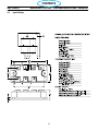
1
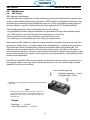
PC 650
TABLE OF CONTENTS
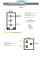
Plasmarc Cutting Console
SAFETY
INTRODUCTION
SPECIFICATIONS
MAIN SCHEMATIC
MAINTENANCE
REPLACEMENT PARTS
Service Manual
This manual provides service / troubleshooting
instructions for PC650 consoles beginning with
Serial Number P*J 623080
Manual # 0558006136 - Rev. 0
9/2006
208/230 Volt
460 Volt
220/230 Volt CE
400 Volt CE
PN: 0558003179
PN: 0558005328
PN: 0558005151
PN: 0558005152
Be sure this information reaches the operator.
You can get extra copies through your supplier.
caution
These INSTRUCTIONS are for experienced operators. If you are not fully familiar with the
principles of operation and safe practices for arc welding and cutting equipment, we urge
you to read our booklet, “Precautions and Safe Practices for Arc Welding, Cutting, and
Gouging,” Form 52-529. Do NOT permit untrained persons to install, operate, or maintain
this equipment. Do NOT attempt to install or operate this equipment until you have read
and fully understand these instructions. If you do not fully understand these instructions,
contact your supplier for further information. Be sure to read the Safety Precautions before installing or operating this equipment.
USER RESPONSIBILITY
This equipment will perform in conformity with the description thereof contained in this manual and
accompanying labels and/or inserts when installed, operated, maintained and repaired in accordance
with the instructions provided. This equipment must be checked periodically. Malfunctioning or
poorly maintained equipment should not be used. Parts that are broken, missing, worn, distorted or
contaminated should be replaced immediately. Should such repair or replacement become necessary, the manufacturer recommends that a telephone or written request for service advice be made
to the Authorized Distributor from whom it was purchased.
This equipment or any of its parts should not be altered without the prior written approval of the
manufacturer. The user of this equipment shall have the sole responsibility for any malfunction
which results from improper use, faulty maintenance, damage, improper repair or alteration by anyone other than the manufacturer or a service facility designated by the manufacturer.
SECTIONS
Safety
Introduction
Specifications
Glossary
Testing / Troubleshooting / Service
1
2
3
4
5
Schematic Section Map
5.0
Input Power Switch
5.1
Input Bridge
Buss Supply
5.2
IGBT Block
5.4
Output Transformer
Output Bridge
5.5
Control Transformer
5.7
PCB1 Control Board
5.8
Output Inductor
5.9
Startup Network
5.10
Fault Circuits
5.11
High Frequency
5.12
Shunt
5.13
Torch
5.14
Maintenance
Replacement Parts
General Information
5.3
5.6
6
7
8
CONTENTS
table of contents
Section / Title
Page
1.0 Safety Precautions . . . . . . . . . . . . . . . . . . . . . . . . . . . . . . . . . . . . . . . . . . . . . . . . . . . . . . . . . . . . . . . . . . . . . . . . . . . . . . . . . . . . 6
2.0 Introduction . . . . . . . . . . . . . . . . . . . . . . . . . . . . . . . . . . . . . . . . . . . . . . . . . . . . . . . . . . . . . . . . . . . . . . . . . . . . . . . . . . . . . . . . . 10
3.0 Power Specifications . . . . . . . . . . . . . . . . . . . . . . . . . . . . . . . . . . . . . . . . . . . . . . . . . . . . . . . . . . . . . . . . . . . . . . . . . . . . . . . . . 11
3.1 208 / 230 Wiring . . . . . . . . . . . . . . . . . . . . . . . . . . . . . . . . . . . . . . . . . . . . . . . . . . . . . . . . . . . . . . . . . . . . . . . . . . . . . . . 12
3.2 Machine Operation Flowchart . . . . . . . . . . . . . . . . . . . . . . . . . . . . . . . . . . . . . . . . . . . . . . . . . . . . . . . . . . . . . . . . . . 16
3.3 PC650 Machine Section Index . . . . . . . . . . . . . . . . . . . . . . . . . . . . . . . . . . . . . . . . . . . . . . . . . . . . . . . . . . . . . . . . . . 16
3.3 Sequence of Operations . . . . . . . . . . . . . . . . . . . . . . . . . . . . . . . . . . . . . . . . . . . . . . . . . . . . . . . . . . . . . . . . . . . . . . . . 17
3.3 Sequence of Operations . . . . . . . . . . . . . . . . . . . . . . . . . . . . . . . . . . . . . . . . . . . . . . . . . . . . . . . . . . . . . . . . . . . . . . . . 18
4.0 Glossary (General Definitions and Symbols) . . . . . . . . . . . . . . . . . . . . . . . . . . . . . . . . . . . . . . . . . . . . . . . . . . . . . . . . . . 19
5.0 Machine Testing / Troubleshooting / Service . . . . . . . . . . . . . . . . . . . . . . . . . . . . . . . . . . . . . . . . . . . . . . . . . . . . . . . . . . 22
5.0 Schematic Section Map 208/230 V 0558003302 . . . . . . . . . . . . . . . . . . . . . . . . . . . . . . . . . . . . . . . . . . . . . . . . . . 22
5.0 Schematic Section Map 460 V 0558005314 . . . . . . . . . . . . . . . . . . . . . . . . . . . . . . . . . . . . . . . . . . . . . . . . . . . . . . 23
5.0 Schematic Section Map 230 V CE 0558005343 . . . . . . . . . . . . . . . . . . . . . . . . . . . . . . . . . . . . . . . . . . . . . . . . . . 24
5.0 Schematic Section Map 400 V CE 0558005314 . . . . . . . . . . . . . . . . . . . . . . . . . . . . . . . . . . . . . . . . . . . . . . . . . . . 25
5.1 Input Power Switch (0558004125) . . . . . . . . . . . . . . . . . . . . . . . . . . . . . . . . . . . . . . . . . . . . . . . . . . . . . . . . . . . . . . . 26
5.2 Input Bridge . . . . . . . . . . . . . . . . . . . . . . . . . . . . . . . . . . . . . . . . . . . . . . . . . . . . . . . . . . . . . . . . . . . . . . . . . . . . . . . . . . . 28
5.3 Buss Supply . . . . . . . . . . . . . . . . . . . . . . . . . . . . . . . . . . . . . . . . . . . . . . . . . . . . . . . . . . . . . . . . . . . . . . . . . . . . . . . . . . . . 30
5.3.1 Buss Supply Schematic . . . . . . . . . . . . . . . . . . . . . . . . . . . . . . . . . . . . . . . . . . . . . . . . . . . . . . . . . . . . . . . . . . . . . . . . . 31
5.3.2 Buss Supply Values . . . . . . . . . . . . . . . . . . . . . . . . . . . . . . . . . . . . . . . . . . . . . . . . . . . . . . . . . . . . . . . . . . . . . . . . . . . . . 32
5.3.3 Buss Supply Testing . . . . . . . . . . . . . . . . . . . . . . . . . . . . . . . . . . . . . . . . . . . . . . . . . . . . . . . . . . . . . . . . . . . . . . . . . . . . 32
5.4 IGBT Block . . . . . . . . . . . . . . . . . . . . . . . . . . . . . . . . . . . . . . . . . . . . . . . . . . . . . . . . . . . . . . . . . . . . . . . . . . . . . . . . . . . . . 33
5.4.1 IGBT Driver Board . . . . . . . . . . . . . . . . . . . . . . . . . . . . . . . . . . . . . . . . . . . . . . . . . . . . . . . . . . . . . . . . . . . . . . . . . . . . . . 33
5.5 Main Transformer T1 . . . . . . . . . . . . . . . . . . . . . . . . . . . . . . . . . . . . . . . . . . . . . . . . . . . . . . . . . . . . . . . . . . . . . . . . . . . 36
5.5.1 Coupling Circuit . . . . . . . . . . . . . . . . . . . . . . . . . . . . . . . . . . . . . . . . . . . . . . . . . . . . . . . . . . . . . . . . . . . . . . . . . . . . . . . . 38
5.5.2 Current Transformer T4 (32958) . . . . . . . . . . . . . . . . . . . . . . . . . . . . . . . . . . . . . . . . . . . . . . . . . . . . . . . . . . . . . . . . . 39
5.6 Output Rectifier 1 (952150) . . . . . . . . . . . . . . . . . . . . . . . . . . . . . . . . . . . . . . . . . . . . . . . . . . . . . . . . . . . . . . . . . . . . . 40
5.7 Control Transformer T2 (35940) . . . . . . . . . . . . . . . . . . . . . . . . . . . . . . . . . . . . . . . . . . . . . . . . . . . . . . . . . . . . . . . . . 42
5.7.1 Axial Fan (951182) . . . . . . . . . . . . . . . . . . . . . . . . . . . . . . . . . . . . . . . . . . . . . . . . . . . . . . . . . . . . . . . . . . . . . . . . . . . . . . 46
5.8 Plasma Control Board (38214) . . . . . . . . . . . . . . . . . . . . . . . . . . . . . . . . . . . . . . . . . . . . . . . . . . . . . . . . . . . . . . . . . . . 47
5.8 Plasma Control Board Schematic (38214) . . . . . . . . . . . . . . . . . . . . . . . . . . . . . . . . . . . . . . . . . . . . . . . . . . . . . . . . 48
5.8.1 PCB1 Control Board and Bias Supplies . . . . . . . . . . . . . . . . . . . . . . . . . . . . . . . . . . . . . . . . . . . . . . . . . . . . . . . . . . . 49
5.8.2 PCB Torch Switch . . . . . . . . . . . . . . . . . . . . . . . . . . . . . . . . . . . . . . . . . . . . . . . . . . . . . . . . . . . . . . . . . . . . . . . . . . . . . . . 51
5.8.3Gas Circuit . . . . . . . . . . . . . . . . . . . . . . . . . . . . . . . . . . . . . . . . . . . . . . . . . . . . . . . . . . . . . . . . . . . . . . . . . . . . . . . . . . . . . 52
5.8.4 Pulse Width Modulator . . . . . . . . . . . . . . . . . . . . . . . . . . . . . . . . . . . . . . . . . . . . . . . . . . . . . . . . . . . . . . . . . . . . . . . . . 53
5.8.5 Overcurrent Sense . . . . . . . . . . . . . . . . . . . . . . . . . . . . . . . . . . . . . . . . . . . . . . . . . . . . . . . . . . . . . . . . . . . . . . . . . . . . . 54
5.8.6 Arc On Circuit . . . . . . . . . . . . . . . . . . . . . . . . . . . . . . . . . . . . . . . . . . . . . . . . . . . . . . . . . . . . . . . . . . . . . . . . . . . . . . . . . . 55
5.8.7 Lock In Switch Circuit . . . . . . . . . . . . . . . . . . . . . . . . . . . . . . . . . . . . . . . . . . . . . . . . . . . . . . . . . . . . . . . . . . . . . . . . . . . 56
5.8.8 Current Control . . . . . . . . . . . . . . . . . . . . . . . . . . . . . . . . . . . . . . . . . . . . . . . . . . . . . . . . . . . . . . . . . . . . . . . . . . . . . . . . 57
5.8.9 Over / Under Voltage Fault Circuit . . . . . . . . . . . . . . . . . . . . . . . . . . . . . . . . . . . . . . . . . . . . . . . . . . . . . . . . . . . . . . 58
5.8.10HF Activation . . . . . . . . . . . . . . . . . . . . . . . . . . . . . . . . . . . . . . . . . . . . . . . . . . . . . . . . . . . . . . . . . . . . . . . . . . . . . . . . . . 59
5.8.11Lock In Switch Circuit . . . . . . . . . . . . . . . . . . . . . . . . . . . . . . . . . . . . . . . . . . . . . . . . . . . . . . . . . . . . . . . . . . . . . . . . . . . 60
5.9 Output Inductor L1 - (952606) . . . . . . . . . . . . . . . . . . . . . . . . . . . . . . . . . . . . . . . . . . . . . . . . . . . . . . . . . . . . . . . . . . . 61
5.10 Startup Board PCB5 - (38131) . . . . . . . . . . . . . . . . . . . . . . . . . . . . . . . . . . . . . . . . . . . . . . . . . . . . . . . . . . . . . . . . . . . . 62
5.11 Trigger Lock Switch S2 . . . . . . . . . . . . . . . . . . . . . . . . . . . . . . . . . . . . . . . . . . . . . . . . . . . . . . . . . . . . . . . . . . . . . . . . . . 63
5.11.1PC650 Fault Monitoring . . . . . . . . . . . . . . . . . . . . . . . . . . . . . . . . . . . . . . . . . . . . . . . . . . . . . . . . . . . . . . . . . . . . . . . . 64
5.11.2Fault Light . . . . . . . . . . . . . . . . . . . . . . . . . . . . . . . . . . . . . . . . . . . . . . . . . . . . . . . . . . . . . . . . . . . . . . . . . . . . . . . . . . . . . 65
5.11.3Flow Switch (951202) . . . . . . . . . . . . . . . . . . . . . . . . . . . . . . . . . . . . . . . . . . . . . . . . . . . . . . . . . . . . . . . . . . . . . . . . . . . 65
5.12 High Frequency (951179) . . . . . . . . . . . . . . . . . . . . . . . . . . . . . . . . . . . . . . . . . . . . . . . . . . . . . . . . . . . . . . . . . . . . . . . 66
CONTENTS
table of contents
Section / Title
Page
5.12.1T3 High Frequency Transformer . . . . . . . . . . . . . . . . . . . . . . . . . . . . . . . . . . . . . . . . . . . . . . . . . . . . . . . . . . . . . . . . 67
5.12.2Spark Gap (0558001180) . . . . . . . . . . . . . . . . . . . . . . . . . . . . . . . . . . . . . . . . . . . . . . . . . . . . . . . . . . . . . . . . . . . . . . . . 68
5.12.3Air Test Switch . . . . . . . . . . . . . . . . . . . . . . . . . . . . . . . . . . . . . . . . . . . . . . . . . . . . . . . . . . . . . . . . . . . . . . . . . . . . . . . . . 69
5.13 Shunt (31488) . . . . . . . . . . . . . . . . . . . . . . . . . . . . . . . . . . . . . . . . . . . . . . . . . . . . . . . . . . . . . . . . . . . . . . . . . . . . . . . . . . 70
5.14 PT31 Torch (0558003183) . . . . . . . . . . . . . . . . . . . . . . . . . . . . . . . . . . . . . . . . . . . . . . . . . . . . . . . . . . . . . . . . . . . . . . . 71
6.0 Maintenance . . . . . . . . . . . . . . . . . . . . . . . . . . . . . . . . . . . . . . . . . . . . . . . . . . . . . . . . . . . . . . . . . . . . . . . . . . . . . . . . . . . . . . . . 72
6.0 IGBT Testing . . . . . . . . . . . . . . . . . . . . . . . . . . . . . . . . . . . . . . . . . . . . . . . . . . . . . . . . . . . . . . . . . . . . . . . . . . . . . . . . . . . 72
6.1 Buss Supply Power Control / IGBT Testing Procedure (1) . . . . . . . . . . . . . . . . . . . . . . . . . . . . . . . . . . . . . . . . . . 73
6.2 Buss Supply Power Control / IGBT Tester Schematic . . . . . . . . . . . . . . . . . . . . . . . . . . . . . . . . . . . . . . . . . . . . . . 75
6.3 Buss Supply Power Control / IGBT / MOSFET Testing . . . . . . . . . . . . . . . . . . . . . . . . . . . . . . . . . . . . . . . . . . . . . 76
6.4 208/230 V Wiring Diagram . . . . . . . . . . . . . . . . . . . . . . . . . . . . . . . . . . . . . . . . . . . . . . . . . . . . . . . . . . . . . . . . . . . . . . 77
6.5 460 V Wiring Diagram . . . . . . . . . . . . . . . . . . . . . . . . . . . . . . . . . . . . . . . . . . . . . . . . . . . . . . . . . . . . . . . . . . . . . . . . . 79
6.6 230 V CE Wiring Diagram . . . . . . . . . . . . . . . . . . . . . . . . . . . . . . . . . . . . . . . . . . . . . . . . . . . . . . . . . . . . . . . . . . . . . . 81
6.7 400 V CE Wiring Diagram . . . . . . . . . . . . . . . . . . . . . . . . . . . . . . . . . . . . . . . . . . . . . . . . . . . . . . . . . . . . . . . . . . . . . . 83
7.0 Replacement Parts . . . . . . . . . . . . . . . . . . . . . . . . . . . . . . . . . . . . . . . . . . . . . . . . . . . . . . . . . . . . . . . . . . . . . . . . . . . . . . . . . . . 85
7.1 General . . . . . . . . . . . . . . . . . . . . . . . . . . . . . . . . . . . . . . . . . . . . . . . . . . . . . . . . . . . . . . . . . . . . . . . . . . . . . . . . . . . . . . . . 85
7.2 Ordering . . . . . . . . . . . . . . . . . . . . . . . . . . . . . . . . . . . . . . . . . . . . . . . . . . . . . . . . . . . . . . . . . . . . . . . . . . . . . . . . . . . . . . . 85
7.3 PC650 Replacement Parts Front . . . . . . . . . . . . . . . . . . . . . . . . . . . . . . . . . . . . . . . . . . . . . . . . . . . . . . . . . . . . . . . . 86
7.4 PC650 Replacement Parts Front Inside . . . . . . . . . . . . . . . . . . . . . . . . . . . . . . . . . . . . . . . . . . . . . . . . . . . . . . . . . . 88
7.5 PC650 Replacement Parts Rear . . . . . . . . . . . . . . . . . . . . . . . . . . . . . . . . . . . . . . . . . . . . . . . . . . . . . . . . . . . . . . . . . 89
7.6 PC650 Replacement Parts Top Inside 2 . . . . . . . . . . . . . . . . . . . . . . . . . . . . . . . . . . . . . . . . . . . . . . . . . . . . . . . . . . 90
7.7 PC650 Replacement Parts Top Inside . . . . . . . . . . . . . . . . . . . . . . . . . . . . . . . . . . . . . . . . . . . . . . . . . . . . . . . . . . . . 92
7.8 PC650 Replacement Parts Top Inside 3 . . . . . . . . . . . . . . . . . . . . . . . . . . . . . . . . . . . . . . . . . . . . . . . . . . . . . . . . . . 93
7.9 PC650 Replacement Parts Left Inside . . . . . . . . . . . . . . . . . . . . . . . . . . . . . . . . . . . . . . . . . . . . . . . . . . . . . . . . . . . . 94
7.10 PC650 Replacement Parts Right Inside 230 . . . . . . . . . . . . . . . . . . . . . . . . . . . . . . . . . . . . . . . . . . . . . . . . . . . . . . 96
7.11 PC650 Replacement Parts Left Inside Detail 460 . . . . . . . . . . . . . . . . . . . . . . . . . . . . . . . . . . . . . . . . . . . . . . . . . 98
7.12 PC650 Replacement Parts Right Inside Detail 460 . . . . . . . . . . . . . . . . . . . . . . . . . . . . . . . . . . . . . . . . . . . . . . . . 99
7.13 PC650 Replacement Parts Outside . . . . . . . . . . . . . . . . . . . . . . . . . . . . . . . . . . . . . . . . . . . . . . . . . . . . . . . . . . . . . 100
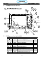
7.14 PC650 Replacement Parts Spreadsheet . . . . . . . . . . . . . . . . . . . . . . . . . . . . . . . . . . . . . . . . . . . . . . . . . . . . . . . . 101
8.0 Solenoid - Potentiometer - LED . . . . . . . . . . . . . . . . . . . . . . . . . . . . . . . . . . . . . . . . . . . . . . . . . . . . . . . . . . . . . . . . 106
8.1 Trouble Shooting Flow Chart . . . . . . . . . . . . . . . . . . . . . . . . . . . . . . . . . . . . . . . . . . . . . . . . . . . . . . . . . . . . . . . . . . 107
8.2 Low Voltage Check . . . . . . . . . . . . . . . . . . . . . . . . . . . . . . . . . . . . . . . . . . . . . . . . . . . . . . . . . . . . . . . . . . . . . . . . . . . . 108
8.3 PT31 Torch . . . . . . . . . . . . . . . . . . . . . . . . . . . . . . . . . . . . . . . . . . . . . . . . . . . . . . . . . . . . . . . . . . . . . . . . . . . . . . . . . . . . 109
Index . . . . . . . . . . . . . . . . . . . . . . . . . . . . . . . . . . . . . . . . . . . . . . . . . . . . . . . . . . . . . . . . . . . . . . . . . . . . . . . . . . . . . . . . . . . . . . .110
4&$5*0/
CONTENTS
4"'&5:13&$"65*0/4
section 1safety precautions
1.0 Safety Precautions
4BGFUZ1SFDBVUJPOT
6TFSTPG&4"#XFMEJOHBOEQMBTNBDVUUJOHFRVJQNFOUIBWFUIFVMUJNBUFSFTQPOTJCJMJUZGPSFOTVSJOHUIBUBOZPOF
XIPXPSLTPOPSOFBSUIFFRVJQNFOUPCTFSWFTBMMUIFSFMFWBOUTBGFUZQSFDBVUJPOT4BGFUZQSFDBVUJPOTNVTUNFFU
UIFSFRVJSFNFOUTUIBUBQQMZUPUIJTUZQFPGXFMEJOHPSQMBTNBDVUUJOHFRVJQNFOU5IFGPMMPXJOHSFDPNNFOEBUJPOT
TIPVMECFPCTFSWFEJOBEEJUJPOUPUIFTUBOEBSESFHVMBUJPOTUIBUBQQMZUPUIFXPSLQMBDF
"MMXPSLNVTUCFDBSSJFEPVUCZUSBJOFEQFSTPOOFMXFMMBDRVBJOUFEXJUIUIFPQFSBUJPOPGUIFXFMEJOHPSQMBTNB
DVUUJOHFRVJQNFOU*ODPSSFDUPQFSBUJPOPGUIFFRVJQNFOUNBZMFBEUPIB[BSEPVTTJUVBUJPOTXIJDIDBOSFTVMUJO
JOKVSZUPUIFPQFSBUPSBOEEBNBHFUPUIFFRVJQNFOU
"OZPOFXIPVTFTXFMEJOHPSQMBTNBDVUUJOHFRVJQNFOUNVTUCFGBNJMJBSXJUI
JUTPQFSBUJPO
MPDBUJPOPGFNFSHFODZTUPQT
JUTGVODUJPO
SFMFWBOUTBGFUZQSFDBVUJPOT
XFMEJOHBOEPSQMBTNBDVUUJOH
5IFPQFSBUPSNVTUFOTVSFUIBU
OPVOBVUIPSJ[FEQFSTPOis TUBUJPOFEXJUIJOUIFXPSLJOHBSFBPGUIFFRVJQNFOUXIFOJUJTTUBSUFEVQ
OPPOFJTVOQSPUFDUFEXIFOUIFBSDJTTUSVDL
5IFXPSLQMBDFNVTU
CFTVJUBCMFGPSUIFQVSQPTF
CFGSFFGSPNESBGUT
1FSTPOBMTBGFUZFRVJQNFOU
"MXBZTXFBSSFDPNNFOEFEQFSTPOBMTBGFUZFRVJQNFOUTVDIBTTBGFUZHMBTTFTnBNFQSPPG
DMPUIJOHTBGFUZHMPWFT
%POPUXFBSMPPTFmUUJOHJUFNTTVDIBTTDBSWFTCSBDFMFUTSJOHTFUDXIJDIDPVMECFDPNF
USBQQFEPSDBVTFCVSOT
(FOFSBMQSFDBVUJPOT
.BLFTVSFUIFSFUVSODBCMFJTDPOOFDUFETFDVSFMZ
8PSLPOIJHIWPMUBHFFRVJQNFOUNBZPOMZCFDBSSJFEPVUCZBRVBMJmFEFMFDUSJDJBO
"QQSPQSJBUFmSFFYUJORVJTIJOHFRVJQNFOUNVTUCFDMFBSMZNBSLFEBOEDMPTFBUIBOE
-VCSJDBUJPOBOENBJOUFOBODFNVTUOPUCFDBSSJFEPVUPOUIFFRVJQNFOUEVSJOHPQFSBUJPO
CONTENTS
section
1safety
precautions
4&$5*0/
4"'&5:13&$"65*0/4
8"3/*/(
8&-%*/("/%1-"4."$655*/($"/#&*/+63*06450:0634&-'"/%
05)&34 5",& 13&$"65*0/4 8)&/ 8&-%*/( 03 $655*/( "4, '03
:063 &.1-0:&34 4"'&5: 13"$5*$&4 8)*$) 4)06-% #& #"4&% 0/
."/6'"$563&34)";"3%%"5"
&-&$53*$4)0$,$BOLJMM
*OTUBMMBOEFBSUIHSPVOE
UIFXFMEJOHPSQMBTNBDVUUJOHVOJUJOBDDPSEBODFXJUIBQQMJDBCMFTUBOEBSET
%POPUUPVDIMJWFFMFDUSJDBMQBSUTPSFMFDUSPEFTXJUICBSFTLJOXFUHMPWFTPSXFUDMPUIJOH
*OTVMBUFZPVSTFMGGSPNFBSUIBOEUIFXPSLQJFDF
&OTVSFZPVSXPSLJOHTUBODFJTTBGF
'6.&4"/%("4&4$BOCFEBOHFSPVTUPIFBMUI
,FFQZPVSIFBEPVUPGUIFGVNFT
6TFWFOUJMBUJPOFYUSBDUJPOBUUIFBSDPSCPUIUPUBLFGVNFTBOEHBTFTBXBZGSPNZPVSCSFBUIJOH[POF
BOEUIFHFOFSBMBSFB
"3$3":4$BOJOKVSFFZFTBOECVSOTLJO
1SPUFDUZPVSFZFTBOECPEZ6TFUIFDPSSFDUXFMEJOHQMBTNBDVUUJOHTDSFFOBOEmMUFSMFOTBOEXFBS
QSPUFDUJWFDMPUIJOH
1SPUFDUCZTUBOEFSTXJUITVJUBCMFTDSFFOTPSDVSUBJOT
'*3&)";"3%
4QBSLTTQBUUFS
DBODBVTFmSF.BLFTVSFUIFSFGPSFUIBUUIFSFBSFOPJOnBNNBCMFNBUFSJBMTOFBSCZ
/0*4&&YDFTTJWFOPJTFDBOEBNBHFIFBSJOH
1SPUFDUZPVSFBST6TFFBSNVõTPSPUIFSIFBSJOHQSPUFDUJPO
8BSOCZTUBOEFSTPGUIFSJTL
."-'6/$5*0/$BMMGPSFYQFSUBTTJTUBODFJOUIFFWFOUPGNBMGVODUJPO
3&"%"/%6/%&345"/%5)&*/4536$5*0/."/6"-#&'03&*/45"--*/(0301&3"5*/(
1305&$5:0634&-'"/%05)&34
CONTENTS
section 1safety precautions
Full responsibility for the safety of personnel working on or near these systems rests on user of ESAB
Welding Equipment.
Incorrect operation can lead to an abnormal situation, injury to the operator and /or damage to the
equipment.
All personnel working with Plasma Cutting equipment must be fully familiar with
- handling of equipment
- location of emergency stops
- functions of equipment
- applicable safety regulations
- Plasma Cutting Process
Operator must make sure
- no one stays inside work area while machine starts
- no one is unprotected while arc is being struck
Work area must be
- free of machine parts, tools and other objects that can obstruct operator moving within the work
area
- so arranged, that emergency stop buttons are easily accessible
- free from draughts
Personal safety equipment
- always use proper safety equipment such as goggles, non flammable clothing, protective gloves
- never wear loose clothing, belts, bracelets, rings etc., which may catch on equipment or cause burns
Miscellaneous
- only authorized personnel may operate connected equipment
- check whether return cables are properly connected and grounded
-required fire fighting equipment should be easily available in specially and clearly marked areas
WARNING
ARC WELDING AND CUTTING CAN BE INJURIOUS TO YOURSELF
AND OTHERS. TAKE PRECAUTIONS WHEN WELDING OR CUTTING.
ASK YOUR EMPLOYER FOR SAFETY PRACTICES THAT SHOULD BE
BASED ON MANUFACTURER’S HAZARD DATA.
CONTENTS
section 1safety precautions
ELECTRIC SHOCK - Can kill
- Install and ground welding equipment in accordance with obligatory standards.
- Do not touch live electrical parts or electrodes with bare skin, wet gloves or wet clothes.
- Insulate yourself from ground and workpiece.
- Ensure your work position is safe.
FUMES AND GASES - Can be dangerous to your health
- Do not breath the fumes.
- Use ventilation and/or extraction to keep fumes and gases away from your breathing zone and surroundings.
FLASH - Can injure eyes and burn skin
- Protect your eyes and skin. Use correct helmet, lenses and wear protective clothes.
- Protect bystanders with suitable screens or curtains.
FIRE HAZARD
- Sparks (spatter) can cause fire. Make sure there are no inflammable materials nearby.
NOISE - Excessive noise can damage your hearing.
- Protect your ears. Use hearing protection.
- Warn bystanders of the risk.
MALFUNCTION - Call expert assistance in event of a malfunction.
CONTENTS
section 2INTRODUCTION
2.0Introduction
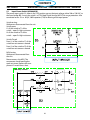
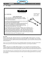
The PC650 is a compact Inverter Plasma unit designed to deliver up to 40 Amps of power at approximately 120 cutting volts. It has an adjustable output and a built in trigger “lock-in” circuit. This lightweight unit is supplied in versions that allow input voltages of 208/230/400/or 460 volts AC.
The system comes equipped with a PT31XL “drag type” torch and a spare parts kit. When connected to a
source of compressed air (250 CFH, 90 – 150 psi), the unit is capable of cutting 5/8” material and severing
¾” with an output current range of 10 to 40A.
2.1 Scope
The purpose of this manual is to provide qualified repair personnel with technical information, which will
assist in troubleshooting and repairing malfunctions
2.2 Service Manual format
The “machine operation” flow diagram starts the breakdown of the functionally of the PC650. Each of the
major components is divided into sections, which are described in the pages that follow. Each section in
the flow chart has a matching section on the main schematic and is applied to the description pages.
Each section starts with the schematic view with description, if the section includes a printed circuit PC
board, it is followed by a PC board schematic, the layout of the board and then the component list for
the board. Some PC boards will also have “mini descriptions” of selected circuits. This information is for
troubleshooting purposes only, PC board repair is not recommended.
10
CONTENTS
section 3
3.0
SPECIFICATIONS
Power Specifications
PC650 Power Specifications
Output:
40% duty cycle
40A/120V
60% duty cycle
30A/120V
100% duty cycle
22A/120V
Output Current Range
10 to 40 Amperes
Open Circuit Voltage
290 Vdc Nominal
Input @ 40A/120V
208/230 vac 1 ph. 50/60 Hz., 35/32 amps
Input @ 40A/120V
460 vac 3 ph. 50/60 Hz., 8/5 amps
Power factor @ 40A Output 76% (1 Phase)
Efficiency @ 40A Output
85% (Typical)
Air requirements
250 cfh at 80 psig
PC650 PHYSICAL INFORMATION
Length
16” (406 mm)
Length w/handles
25.70” (653 mm)
Height
16.38” (416 mm)
Width
12.50” (318 mm )
Weight
53 lbs (16 kg)
Shipping Weight
71 Lbs ( 32.3 Kg)
208/230 Volt PN: 0558003179 Console only
460 Volt
PN: 0558005328 Console only
The Powercut 650 is available as 208/230 VAC single-phase power, or as 460 VAC 3 phase.
The 208/230 volt model comes configured from the factory for 230 VAC operations. If using a 208 VAC
source for operation, the Powercut 650 must be reconfigured before using a 208 VAC source (See Section
3.1).
Note: The 460 VAC 3 phase unit is designed to work best when 3 phase input power is used, however
with a slight de-rating of the machine output, the PC650 can be used on single phase.
Reasons for de-rating:
Input diode stress. 1 phase uses 4 diodes at higher current levels
Buss capacitors will see higher ripple currents
11
CONTENTS
section 3
3.1
SPECIFICATIONS
208 / 230 Wiring
PC650 CE Power Specifications
Output:
40% duty cycle
40A/120V
60% duty cycle
30A/120V
100% duty cycle
22A/120V
Output Current Range
10 to 40 Amperes
Open Circuit Voltage
290 Vdc Nominal
Input @ 40A/120V
220/230 vac 1 ph. 50/60 Hz., 37/20 amps
Input @ 40A/120V
400 vac 3 ph. 50/60 Hz., 9 amps
Power factor @ 40A Output 76% (1 Phase)
Efficiency @ 40A Output
85% (Typical)
Air requirements
118 l/m @ 5.5 bar
PC650 CE PHYSICAL INFORMATION
Length
406 mm
Length w/handles
653 mm
Height
416 mm
Width
318 mm
Weight
Shipping Weight
16 kg
32.3 Kg
220/230 Volt PN: 0558005151 Console only
400 Volt
PN: 0558005153 Console only
The Powercut 650 “CE model” is available as 230 VAC single-phase power, or as 400 VAC 3 phase.
Note: The 400 VAC 3 phase unit is designed to work best when 3 phase input power is used, however with a slight de-rating
of the machine output, the PC650 can be used on single phase.
Reasons for de-rating:
Input diode stress. 1 phase uses 4 diodes at higher current levels
Buss capacitors will see higher ripple currents
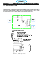
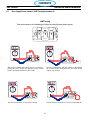
Connecting PC650 for 208 VAC input:
1. Unplug the unit from the primary input power.
2. Remove the left side panel by removing the rear handle and sliding the cover forward from the aluminum frame
rail.
3. Locate the input bridge (IBR) and the two-position terminal block on the left side of the unit towards the rear
panel. Locate the gray wire connected
to TB5-2 and to IBR terminal “R”. For 208-vac input, disconnect the gray wire from TB5-2 and then firmly connect it
to TB5-1.
4. Locate the output bridge (D1) on the left side towards the front panel. Disconnect and swap leads X2 and X3
from the main transformer. For 208 VAC input, X2 is connected to TB3 and X3 is connected to terminal 3 of D1.
Make sure the connections are firmly tightened.
5. Leave all other wires the same.
6. Reinstall cover by sliding it back into the frame rail. Connect the front handle and connect the Powercut 650 to
the 208 VAC input power.
12
CONTENTS
section 3
3.1
SPECIFICATIONS
208 / 230 Wiring
13
CONTENTS
section 3SPECIFICATIONS
3.1
208 / 230 Wiring
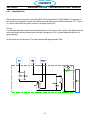
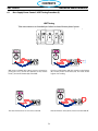
CONNECTIONS
ELECTRIC SHOCK CAN KILL! Precautionary measures should be taken to provide
maximum protection against electrical
shock. Be sure that all power is off by
opening the line (wall) disconnect switch
and by unplugging the power cord to the
unit when connections are made inside of
the power source.
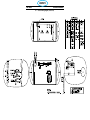
PRIMARY ELECTRICAL INPUT CONNECTIONS
FIGURE 3.1
A line (wall) disconnect switch with fuses or circuit breakers should be provided at
the main power panel (see Fig. 3-1 and Table 3-1 for fuse sizes). The input power
cable of the console may be connected directly to the disconnect switch or you
may purchase a proper plug and receptacle from a local electrical supplier. If using
plug/receptacle combination, see Table 3-1 for recommended input conductors for
connecting receptacle to line disconnect switch.
Be sure that the power source is properly
configured for your input power supply. DO
NOT connect a power source configured for
208/230 V to a 460 V input power supply.
Damage to the machine may occur.
NOTE: PC650 input cable differences
The colors of input phases of the CE models differ from those of the “non CE” models. Below is a table
comparing the two:
Input
L1
L2
L3
GND
Standard
Black
Red
White
Green
Input
L1
L2
L3
GND
CE
Brown
Grey
Black
Green/Yellow
400 & 460-Volt CE
For the 400 and 460-Volt units, it isn’t important which leg is connected to L1, L2 and L3, when 3-Phase
input is used, however if inputting 1 phase power, L2 will be the un-used leg. The T2 must have power to
operate and it is connected across L1 and L3.
208/230-Volt models
**FOR SINGLE-PHASE CONNECTION OF 230-Volt CE MODELS:**
If single-phase connection is desired, connect the BLACK leg to “L3” and the BROWN leg to “L1” with the GREY
(L2) leg disconnected, lugged, and taped back. , L2 will be the un-used leg. The T2 must have power to
operate and it is connected across L1 and L3
14
CONTENTS
section 3SPECIFICATIONS
3.1
208 / 230 Wiring
Recommended Sizes for Input Conductors and Line Fuses
Rated Input
Volts
Amp
Phases
208
35
230
32
400
9
1
1
3
460
8
3
Input & GND Conductor
CU/AWG*
Fuse Size
No. 10
No. 10
No. 12
No. 12
50
Amps
50
15
15
* Sized per National Code for 80°C rated copper conductors @ 30°C ambient. Not more than
three conductors in raceway or cable. Local codes should be followed if they specify sizes other
than those listed above.
CUSTOMER FUSED LINE DISCONNECT SWITCH (See Table
3.1 and WARNING in regards to
chassis ground in Section 3.4)
Factory supplied primary
power cable with plug.
Figure 3.1 Customer Fused Line Disconnect and Receptacle
15
CONTENTS
section 3
3.2
SPECIFICATIONS
Machine Operation Flowchart
3.3
PC650 Machine Section Index
Section Index
Sec. #5.
Section Name
Page
Sec. #5.
Section Name
Page
1
Input Switch S3
30
10
PCB5 Start-up Network
67
2
Input Bridge
32
11
Fault Circuits
68
3
Buss Supply
34
12
High Frequency
71
4
IGBT Block
37
13
Shunt
75
5
Output Transformer T1
40
14
Torch
76
6
Output Bridge
44
7
Control Transformer T2
46
8
PCB1 Control Board
51
9
Output Inductor
66
16
CONTENTS
section 3
3.3
SPECIFICATIONS
Sequence of Operations
17
CONTENTS
section 3
3.3
SPECIFICATIONS
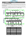
Sequence of Operations
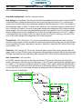
1.
The operator engages the torch switch on the torch, requesting a cutting operation. This closes
the torch switch connection at the control PCB (P5-1, P5-2). This enables the torch switch circuit, which,
ultimately, sends two logic signals out of that circuit. One signal leaves IC1-4 to enable the control chip
IC2 on PCB-1. The other signal leaves IC9-5 destined for the current control logic chip IC10 –1 via D22.
The start LED, LED1, lights up indicating start voltage is present. See Section 5.8.2.
2.
The gas flow solenoid is engaged and air moves through the torch.
section
3
sPeciFicAtions
3.
The Flow Switch closes.
4.
After a 2 second preflow delay, PCB1 relay K1 closes sending 115 VAC out to the HF circuit. The Spark Gap unit, SG, engages.
5.
IGBTs’sequence
are gated on
open circuit voltage is available at the torch
3.3
of and
operation
6.
The operator brings the torch nozzle in contact with the work surface
7.
The HF signal ionizes the air and sets an environment conducive to main arc creation.
8.
Main arc is established.
SEQUENCE OF
OPERATION
Trigger LOCK “UnLocK” position (Applies to PT-21AMX and PT-32EH Torches)
Push
Release
Torch Switch
Open
Close
Gas Solenoid Valve
2 sec.
Preflow
20 sec.
Postflow
Open
Close
Flow Switch
Fault Overload Light
HF Circuit
Energize
Pilot Arc
Inverter
Cutting Arc (Current)
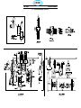
notes:
1. When the torch switch is pushed during postflow period, the postflow and preflow times are canceled, and the HF is
energized immediately.
2. When the red fault light comes on, cutting operation should be stopped. The postflow time starts from the moment the
torch switch is released.
18
11
CONTENTS
SECTION 4GLOSSARY
4.0Glossary (General Definitions and Symbols)
SYMBOL
NOTATION
NAME
VALUES
A
Amperage
n
Current: effectively the "amount of flow" of electricity.
V
Volts
n
Electromotive force: effectively the "pressure" of electron movement.
R
Resistance
n
Opposition to electron transfer: expressed in OHMS.
W
Watt
n
A measure of Power. Watts = V*A
F
Farad
n
Amount of electrical storage in a capacitor.
A voltage used to control or stabilize an electronic circuit. A forward bias
is voltage applied in the direction of the current flow within a transistor,
tube or circuit. A reverse bias is voltage applied in the opposite
direction.
BIAS
OCV
+
or
-
+
DESCRIPTION
n VOLTS
Open Circuit Voltage:
n
Number
µ
micro
+
ANODE:
+ Positive element of device.
-
CATHODE:
- Negative element of device - the banded end of a diode.
Cn
CAPACITOR
µF
Cn
ELECTROLITIC
CAPACITOR
µF
Rn
RESISTOR
Fn
FUSE
n A, n V
Device in series with a load which opens the circuit if its current
rating (A) is exceeded.
SW n
SWITCH
n A, n V
n P, n T
Device which opens and closes a circuit.
Dn
DIODE
A semi-conductor that conducts in only one direction
Dn
ZENER DIODE
A diode that permits high current flow without damage, the reverse
voltage remains almost constant over a wide range of currents, used
esp. to regulate voltage.
Dn
LIGHT EMITTING
DIODE
Semiconductor diode that emits light when conducting current
SCR
SILICON
CONTROLLED
RECTIFIER
Device having primary and secondary inductors for altering a-c signal
amplitudes, impedance matching,and isolation purposes. . A reverse
blocking triode thyristor
Ln
COIL
Wound wire device; current through the coil generates a electromagnetic field causing inductive reactance, which increases with
number of turns and density.
Ln
COIL (Iron Core)
Tn
TRANSFORMER
GROUND
Indicates that any number may be used in its place.
0.00000n One Millionth of any unit.
Ω, W
Stores energy in the electrostatic field generated between two metal
plates separated by an insulator. Typical values are in µF.
Electrolitic capacitors will be damaged if polarity is not correct. Capacitors can charge themselves from ambient electric fields and should be
handled with caution.
Component that opposes current flow proportionately to its Ohm (Ω)
rating. Power dissapation is expressed in Watts (Ω).
Adding a core to a coil increases the inductance produced.
Wound wire device with a primary and secondary coil(s) which increases
or decreases voltage applied to the primary based on coil and core
configuration. 1:1 transformers are used for isolation.
Identifies the earth (ground) connection. NOTE: Not for a protective
earth connection.
19
CONTENTS
SECTION 4GLOSSARY
4.0Glossary (General Definitions and Symbols)
SYMBOL
NOTATION
VALUES
DESCRIPTION
NEUTRAL
Electronic neutral or common.
PLUG
CONNECTION
Variously configured male/female separable connectors.
SOL n
SOLENOID
Electro-magnetically operated valve.
Mn
MOTOR
ltr
Mn
NAME
n Ø,HP,V
A device which converts electrical energy to mechanical energy (motion).
A resistor whose resistance changes with temperature.
THERMISTOR
T SW n
THERMAL
SWITCH
Qn
TRANSISTOR
A small base current controls the larger collector current.
TP n
TEST POINT
Dedicated location for obtaining quantification.
Kn
RELAY
Protective device that protects circuits from over temperature.
Collector
A transistor amplifies current.
Base
Emitter
or
n
n
n
n
n
or
or
or
n A, n V
WIRE NODE
Yn
CRYSTAL
LAMP
Electro-mechanical device for opening / closing a circuit.
Schematic representation of physical connection of wires.
n MHz
Device using the mechanical resonance of a physical crystal of piezoelectric material to create an electrical signal with a very precise
frequency.
Produces light by heating a filament.
20
CONTENTS
SECTION 4
4.0
GLOSSARY
Glossary (General Definitions and Symbolsl)
LOGIC SYMBOLS
NAME
SYMBOL
DESCRIPTION
An AND gate can have two or more inputs. The output of an AND gate is
true when all its inputs are true.
AND
INPUT
A
B
X
A
0
0
1
1
AND GATE
OUTPUT
B
0
1
0
1
X = AB
0
0
0
1
An OR gate can have two or more inputs. The output of an OR gate is
true when at least one of its inputs is true.
OR
INPUT
A
B
X
A
0
0
1
1
OR GATE
B
0
1
0
1
OUTPUT
X = A+B
0
1
1
1
A NAND gate can have two or more inputs. The 'o' on the output means
'not' showing that it is a Not AND gate. The output of a NAND gate is
true unless all its inputs are true.
NAND
A
B
X
INPUT
NAND GATE
A
0
0
1
1
OUTPUT
B
0
1
0
1
X=A B
1
1
1
0
A NOR gate can have two or more inputs. The 'o' on the output means
'not' showing that it is a Not OR gate. The output of a NOR gate is true
when none of its inputs are true.
NOR
INPUT
A
B
A
X
X
A
0
0
1
1
NOR GATE
NOT
(INVERTER)
OUTPUT
B
0
1
0
1
X=A+B
1
0
0
0
A NOT gate can only have one input. The 'o' on the output means 'not'.
The output of a NOT gate is the inverse (opposite) of its input, so the
output is true when the input is false. A NOT gate is also called an
inverter.
NOT
INPUT
A
0
1
21
OUTPUT
X=A
1
0
CONTENTS
section 5
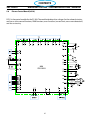
MACHINE TESTING / TROUBLESHOOTING / SERVICE
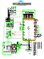
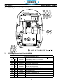
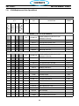
5.0Schematic Section Map 208/230 V 0558003302
1
2
7
3
11
8
11
4
5
13
6
9
10
12
CONTENTS
section 5
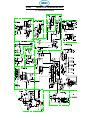
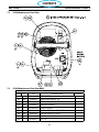
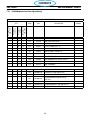
MACHINE TESTING / TROUBLESHOOTING / SERVICE
5.0Schematic Section Map 460 V 0558005314
7
1
2
3
11
4
5
6
13 10
9
11
8
12
CONTENTS
SECTION 5
MACHINE TESTING / TROUBLESHOOTING / SERVICE
5.0Schematic Section Map 230 V CE 0558005343
1
7
2
3
11
4
5
6
13
9
10
8
12
11
CONTENTS
section 5
MACHINE TESTING / TROUBLESHOOTING / SERVICE
5.0Schematic Section Map 400 V CE 0558005314
7
1
2
3
11
4
5
6
13
9
10
8
12
11
CONTENTS
SECTION 5
MACHINE TESTING / TROUBLESHOOTING / SERVICE
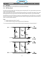
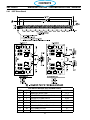
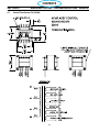
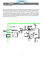
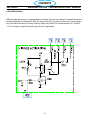
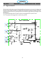
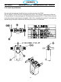
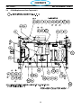
5.1Input Power Switch (0558004125)
The power input switch S3, when in the “ON” position, passes the input voltage, either 208 or 230 VAC, to
the input bridge IBR. Across the switch is a 275V, Metal Oxide Varistor (MOV1) for surge protection. Also
connected across S3 is a .047µF, 300V capacitor (C20) for filtering of the input power.
Switch testing:
With power disconnected from the unit:
Switch open:
L1 of the switch to T1 of the
switch - open Or High resistance
L3 of the switch to T3 of the
switch - open Or High resistance
Switch Closed:
From L1 of the switch to T1 of the
switch low resistance or shorted
From L3 of the switch to T3 of the
switch low resistance or shorted
MOV testing:
With power disconnected from
the unit:
Measure across the MOV. The
component should read high or
open resistance. Replace the component if it reads low or short.
460 Volt, 3 Phase
26
CONTENTS
SECTION 5
MACHINE TESTING / TROUBLESHOOTING / SERVICE
5.1Input Power Switch
PN: 0558004125 (208 / 230 V Units)
PN: 36107 (400 / 460 V Units)
27
CONTENTS
SECTION 5
MACHINE TESTING / TROUBLESHOOTING / SERVICE
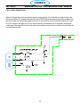
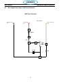
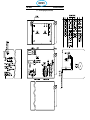
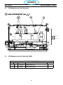
5.2Input Bridge
Single-phase 208 or 230 VAC power enters the rectifier block where it is rectified by the IBR and gated on
and off by an SCR. The rectified 325 VDC output (230VAC input) is coupled to the Bus Supply via L2 on
the negative side of the bridge, and is directly coupled to the IGBTs on the positive side.
L2 is an inductor that has 2 purposes. First to prevent the initial surge of current from damaging the
bridge rectifier and second as a bus filter device, assisting in DC ripple reduction.
SCR (Silicon Controlled Rectifier) is used as a series switch for the DC power during plasma operation.
The SCR is gated on by the PWM on PCB1 and is on when cutting and off when unit is at idle conditions.
During initial charging of the buss caps, power flows through the “precharge” resistor (R10), but when
cutting, R10 is bypassed by the SCR.
IBR Testing
Mode
Ω
Forward Resistance
500 K
Reverse Resistance
(out of circuit)
20 Meg+
Reverse Resistance
(in circuit)
99 K
Testing: 500 K Ohm forward resistance, reverse resistance - high resistance (20 Meg ohm or greater) out
of circuit. In circuit resistance is 99 K Ohm.
208/230 Volt
460 Volt
28
CONTENTS
SECTION 5
MACHINE TESTING / TROUBLESHOOTING / SERVICE
5.2Input Bridge
29
CONTENTS
SECTION 5
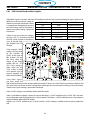
5.3
MACHINE TESTING / TROUBLESHOOTING / SERVICE
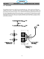
Buss Supply
Capacitor Information
caution
Serious Shock Possible!
Buss cap warning
Serious Shock Possible
The “buss capacitors” in the PC650 will maintain a voltage
charge for approximately 2 minutes after power is removed
from the input of the machine.
The arcing caused by discharging a capacitor into a short-circuit
can cause injury and component damage
To eliminate the voltage from the capacitor, connect the “bleeder resistor” across the poles of a charged capacitor and the
stored energy will discharge harmlessly through the resistor.
The approximate discharge time is 30 seconds.
When discharged, the cap can be partially tested by using a multimeter set to
the ohms scale. When checking a capacitor…Connect the + meter lead to the +
pole of the capacitor, and the – lead to the – pole. The meter display will show
a number that will change while the leads are connected, if the meter leads are
reversed, the display will change polarity and the value will change in the opposite direction from the first test, if the capacitor is good.
BLEEDER RESISTOR
6” Min. 16AWG
600 V Insulation
208 / 230 Volt
The buss supply of the 208 / 230 Volt PC 650 consists of 2 paralleled, 1000μF, 450Vdc capacitors (C1 & C2) that
charge up to the rectified DC voltage output from the input bridge (IBR). This stored voltage is input to the highspeed switching transistors (IGBTs) and inverted to form high frequency, square-wave AC that is then input to the
main transformer (T1).
Across C1 & C2 are 4, 50kΩ/12W resistors and a 1μF, 630Vdc capacitor. The capacitor, C3 and the resistors reduce
electrical noise, plus the resistors provide a discharge path for the buss caps during “off” conditions.
460 Volt
The buss supply consists of 2 1000μF, 400Vdc capacitors (C1 & C2), connected in series that charge up to the
rectified DC voltage output from the input bridge (IBR). This stored voltage is input to the high-speed switching
transistors (IGBTs) and inverted to form high frequency, square-wave AC that is input to the main transformer (T1).
Across each of the series caps is an RC network, which is comprised of a 10kΩ resistor in parallel with a 1μF capacitor. This network is used for noise reduction, plus the resistors provide a discharge path for the buss caps during
“off” conditions.
30
CONTENTS
SECTION 5
MACHINE TESTING / TROUBLESHOOTING / SERVICE
5.3.1 Buss Supply Schematic
208 / 230 Volt
460 Volt
31
CONTENTS
SECTION 5
MACHINE TESTING / TROUBLESHOOTING / SERVICE
5.3.2 Buss Supply Values
Buss Supply Values & Testing
208 / 230 Volt Model
The buss supply for the 208/230 Volt model of the PC650 consists of 3 capacitors and 4 resistors. R2, R15, R16 & R17
are all 50kΩ12Wresistors. The resistors are used for providing a discharge path for the buss supply. C3, a 1μF /
630Vdc capacitor, is used primarily for filtering.
The key components in the buss are the polarized capacitors, C1 & C2. These two caps are both 1000μF
/ 450Vdc capacitors. The buss can be measured across either cap because they are connected in parallel. To measure this buss, connect the positive (red) lead of a voltmeter to “+” post of either buss cap and
the negative (black) lead to the “-“ of the same cap. The nominal buss voltage value is 325Vdc. However,
since the tolerance of the input voltage is +/- 15%, the range of acceptable voltage buss readings is 277
– 375Vdc.
--WARNING---Buss caps can maintain a charge for some time after input power has been removed from the system.
It is imperative that these caps be discharged before testing. It is recommended that a bleeder resistor be used to
discharge the buss caps. The specifications of which should be approximately a 20kΩ, 20W resistor with high voltage insulation on its leads.
--See beginning of section 5.3 for details-460 Volt Model
The 460 Volt model of the PC650 consists of 4 caps and 2 resistors. Capacitors C15 & C3 (1μF, 630Vdc) are used for
filtering and resistors R15 & R2 (10kΩ, 20W) are used for providing a discharge path.
C1 & C2 (1000μF, 400Vdc) are the main buss components and because C1 & C2 are connected in series in the 460 Volt
model, the buss voltage is divided in half, with ½ of the buss voltage being across C1 and the other ½ being across
C2. To measure the total voltage, place the positive (red) lead on the “+” of the C1 and the negative (black) lead on
the “-“ of C2.
Ideally, the buss should read 650Vdc with 325Vdc being across C1 and 325Vdc being across C2. Due to the +/- 15%
tolerance of the input would yield a total buss voltage (across C1 & C2) of 553 – 748Vdc.
It is recommended to use a bleeder resistor to discharge the buss caps.
5.3.3 Buss Supply Testing
Testing Buss Capacitors
The buss capacitors can be easily tested to insure that they are good. It is recommended that a capacitance meter
be used to measure the capacitance, however, a good indication of a good cap can be determined by conducting
an ohms test.
With the machine powered down and caps fully discharged, place the red lead of a voltmeter, in the ohms scale, on
the “+” post of the buss cap and the black lead on the other post of the same cap. The resistance reading should be
in the MΩ range and should be increasing. Reverse the leads and the resistance reading should remain in the MΩ
range, however, the value should be decreasing.
Again, this is only a “good indication” that the capacitor is good. It is still recommended that the capacitance be checked with a capacitance meter.
32
CONTENTS
SECTION 5
MACHINE TESTING / TROUBLESHOOTING / SERVICE
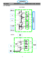
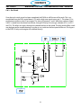
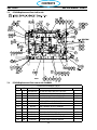
5.4IGBT Block
The Inverter block consists of the IGBT driver board and the IGBT block.
5.4.1IGBT Driver Board
The IGBT driver board conditions the 13 VAC gating signals coming from PCB1. This is done to reduce noise on these
signals and also to protect the IGBTs.
Signals are passed from the secondary of the PCB1 pulse transformer (T1) to the IGBT driver boards. These signals
feed through the driver board and connect to the IGBT module. Each IGBT module has a driver board attached.
The IGBT block consists of 2 IGBT devices mounted on a corresponding heat sink. Each IGBT device is a pair of IGBT
transistors contained within a single package. These devices function as high-speed switches to convert 325VDC to
325VAC. See test procedure Section 6.2.
Testing:
• Perform continuity test on fuse F1 and F2.
• Perform diode test on the four zener diodes to insure 0.7V diode drop
***It is recommended that both IGBTs and both IGBT driver boards be replaced if one is found to be faulty***
33
CONTENTS
SECTION 5
MACHINE TESTING / TROUBLESHOOTING / SERVICE
5.4.1IGBT Driver Board
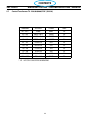
IGBT DRIVER BOARDS REPLACEMENT PARTS
ITEM
QTY
DESCRIPTION
2
4
6
7
8
2
4
2
2
2
CAPACITOR, .047UF @ 63V
DIODE, ZENER 18V, 2W 5% (1N4746A)
RESISTOR, 47.5 OHM 1/2W 1%
RESISTOR, 1K 1/2W 1%
RESISTOR, 2.74 OHMS 1/2W 1%
C1,2
ZD1-ZD4
R1,R2
R3,4
R5,6
10
11
16
4
AR
2
TERMINAL, FASTON .110TSX22-18GA
PLUG COMBICON 5 POS
FUSE, 1/2 AMP
P1
F1,2
34
SYMBOL
CONTENTS
SECTION 5
MACHINE TESTING / TROUBLESHOOTING / SERVICE
5.4.2IGBT Block
208 / 230 Volt
460 Volt
35
CONTENTS
SECTION 5
5.5
MACHINE TESTING / TROUBLESHOOTING / SERVICE
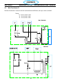
Main Transformer T1
The Main Transformer T1 takes the 325 VAC received from the IGBT block, and steps it down to 290 VAC.
Testing:
H1 – H2 Less than 1 Ohm
X1 – X2 Less than 1 Ohm
X1 – X3 Less than 1 Ohm
208 / 230 Volt
460 Volt
36
CONTENTS
SECTION 5
5.5
MACHINE TESTING / TROUBLESHOOTING / SERVICE
Main Transformer T1 (35941)
37
CONTENTS
SECTION 5
MACHINE TESTING / TROUBLESHOOTING / SERVICE
5.5.1 Coupling Circuit
The coupling circuit consists of resistor R9 (39kΩ, 2W) and capacitor C4 (20μF, 400Vdc). The purpose of
this network is to prevent DC power from flowing into the primary of the main transformer (T1). C4 acts
as a short to the 20 KHz AC power and acts as an open circuit to DC.
Testing:
It is recommended that a capacitance check be done on C4; however, with a meter in the diode scale the
value read should increase showing that the cap is charging up. This is a good indication that this is a
good capacitor.
For R9, perform a resistance test. The meter should read approximately 39kΩ.
38
CONTENTS
SECTION 5
MACHINE TESTING / TROUBLESHOOTING / SERVICE
5.5.2 Current Transformer T4 (32958)
Current transformer (T4) measures the current flowing through the primary of the main transformer (T1).
If this current is too high (100 amps), a signal (1 volt) is sent to the control board via P1-7 and P1-8 to the
over current circuitry (IC2, pin 3) that will indicate an over current fault on the PC650.
39
CONTENTS
SECTION 5
MACHINE TESTING / TROUBLESHOOTING / SERVICE
5.6Output Rectifier 1 (952150)
The Bridge diode D1 is a full wave bridge rectifier, which converts the IGBT’s 290 VAC output to dc volts
which is supplied to the shunt and output inductor (L1). Due to the tolerance of the inputs, the range of
values for this dc voltage is from 260Vdc to 290Vdc. The resistors in the circuit, R3 through R6, as well as
capacitors C5 through C8 are used for electrical noise suppression.
Testing:
With the unit shut down, disconnect the diode from the circuit and test it with an Ohmmeter in the
diode scale. Be mindful that the middle ac input post is not connected on the output bridge. Viewing the
diode with the positive / negative terminals to the left, the 3 ac input terminals are number 1 through 3
from top to bottom although this is not denoted on the diode itself.
To test, perform the following diode voltage checks:
Output Bridge Diode Voltage Checks
Probe (+)
Probe (-)
Value (V)
-
3
0.3
1
+
0.3
Post #2 is not connected
40
CONTENTS
SECTION 5
MACHINE TESTING / TROUBLESHOOTING / SERVICE
5.6Output Rectifier 1 (952150)
41
CONTENTS
SECTION 5
5.7
MACHINE TESTING / TROUBLESHOOTING / SERVICE
Control Transformer T2 (35940)
This transformer supplies reduced AC voltages to the PCB1 control board. It receives 230 volts on the H1
(red) and H3 (gray) leads on the primary, which is stepped down to multiple secondary voltages (See the
accompanying chart).
For the PC 650, the X1- X2 winding feeds 12VAC to the torch switch circuit. The X3-X4 18VAC winding is
not connected. The X5-X6 winding sends 12VAC to the –12VDC bias supply. Winding X7-X8 sends 24VAC
to the gas relay. The X9 – X10 winding sends 20VAC to the +12 & +15VDC bias supplies.
208 / 230 Volt
460 Volt
WINDING
RESISTANCE VALUE ± 15%
VAC ± 15%
H1 - H2
20 OHMS
208V, 50/60 Hz
H1 - H3
23 OHMS
230V, 50/60Hz
H1 - H4
43 OHMS
400V, 50/60 Hz
X1 - X2
1.2 OHMS
12.3V ± .2
X3 - X4
1.6 OHMS
18.3V ± .2
X5 - X6
1.2 OHMS
12.3V ± .2
X7 - X8
2.4 OHMS
24.9V ± .2
X9 - X10
2.0 OHMS
20.3V ± .2
X11 - X12
9.5 OHMS
125 V ± 1.0
42
CONTENTS
SECTION 5
5.7
MACHINE TESTING / TROUBLESHOOTING / SERVICE
Control Transformer T2 (35940)
43
CONTENTS
SECTION 5
5.7
MACHINE TESTING / TROUBLESHOOTING / SERVICE
Control Transformer T2 - 230/400/460/575V (332914)
TERMINAL
VOLTAGE
TURNS
AWG
H1 - H2 *
H1 - H3
H1 - H4
H1 - H5
X2 - X2
X3 - X4
X5 - X6
X7 - X8
X9 - X10
X11 - X12
230.0
402.5 ± 0.4
460.0 ± 0.4
575.0 ± 0.4
24.8 ± 0.5
20.2 ± 0.4
12.4 ± 0.4
18.4± 0.4
12.4 ± 0.4
125 ± 0.4
600T
1050T
1200T
1500T
65T
53T
32T
48T
32T
326T
26
26
26
26
25
25
25
25
25
25
* H1 - H2 COIL IS EXCITATION WINDING
44
CONTENTS
SECTION 5
5.7
MACHINE TESTING / TROUBLESHOOTING / SERVICE
Control Transformer T2 - 230/400/460/575V (32914)
45
CONTENTS
SECTION 5
MACHINE TESTING / TROUBLESHOOTING / SERVICE
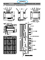
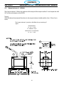
5.7.1Axial Fan (951182)
Active device cooling (the IGBTs, IBR and D1) is performed by axial fan M1.
This fan is connected across the 230-volt primary of the T2, and is on while the PC650 is in operation.
Open circuit resistance is 150 Ohms.
Specifications:
5.9 DIA. x 2.16 In., 247.2 CFM
230V 60Hz/ 55dB(A)/ -40 ~ +55°C
Metal housing and impeller
Shaded pole motor, air output over struts
Elec. connection via 2 leads AWG 18, 14 in. (365 mm) from outer edge of housing.
Mass = 38.8 oz (1100g)
AC AXIAL FAN
5.9 DIA. x 2.16 In., 247.2 CFM
230V 60Hz/ 55dB(A)/ -40 ~ +55°C
Metal housing and impeller. Shaded pole motor, air output over struts.
Elec. connection via 2 leads AWG 18, 14 in. (365 mm) from outer edge of housing.
Mass = 38.8 oz (1100 g).
0
100
200
300
Static Pressure
.5
6.375
400
.6
in. H2O
500 m3/hr
150
Pa
60 Hz
50 Hz
.4
.3
.2
50
.1
6.75
0
0
0
2.1875
100
5.875 OD
46
50
100
150
200
250 300 CFM
CONTENTS
SECTION 5
5.8
MACHINE TESTING / TROUBLESHOOTING / SERVICE
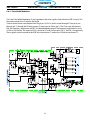
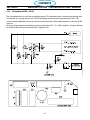
Plasma Control Board (38214)
PCB 1 is the control module for the PC 650. The module develops bias voltages for the onboard circuitry,
and has on it the control functions, PWM functions, error functions (current limit, over current detection)
and Arc on circuitry.
47
CONTENTS
section 5
MACHINE TESTING / TROUBLESHOOTING / SERVICE
5.8
Plasma Control Board Schematic (38214)
CONTENTS
SECTION 5
MACHINE TESTING / TROUBLESHOOTING / SERVICE
5.8.1 PCB1 Control Board and Bias Supplies
BIAS POWER SUPPLIES
The PCB1Control Board creates 4 bias voltages for circuit function. These voltages are +/- 12 volts DC, +15 Volts
DC and +5 volts DC. This provides operating voltages to the Pulse Width Modulator (PWM), the control circuit, the
torch switch circuit, the over current protection circuit and the arc on circuit.
Positive 12 and 15 volts are created on the board by VR1 and VR2 respectively. This circuit receives 20 Volts AC from
the PCB module control transformer on the connector plug P1 pins 3 and 4 (P1-3, P1-4). The voltage is applied to
BR2, a full wave bridge rectifier and converted to pulsating DC. The pulsating DC is then filtered by filter capacitor C32, a 1000 Microfarad capacitor, and fed to a 3-pin voltage regulator, VR1, an LM 7815 +15 volt regulator. The
positive DC is input on pin one of the regulator and outputted on pin 3. Pin 2 of the regulator is tied to ground.
The 15-volt output is then connected to C31, a 47 Microfarad capacitor for ripple and noise suppression, and then
distributed throughout the board.
Filtered DC from the rectifier circuit is also fed to VR2, an LM7812 3 pin voltage regulator. The capacitor C63, a 1000microfarad capacitor, is installed for additional filtering before applying voltage to pin 1 of the regulator. The Positive 12 volt output is derived from pin 3 of the regulator, and then fed across C30, a 47 Microfarad capacitor for ripple
and noise suppression, and then distributed throughout the board.
Capacitor C33 is installed ahead of the rectifier bridge for noise suppression
Negative 12-volt power is created by VR3, An LM7912 3 pin voltage regulator. 12 Volt power from the mains module
control transformer is supplied to the rectifier bridge via connector plug P1 pins 5 and 6 (P1-5, P1-6). The voltage is
applied to BR3, a full wave bridge rectifier and converted to pulsating DC. The pulsating DC is then filtered by filter
capacitor C35, a 1000-microfarad capacitor. The filtered DC is then applied to pin 2 of the LM7912, a negative 12 volt
3 pin voltage regulator chip. Pin one is connected to the negative output of the Rectifier Bridge and negative 12 volts
is distributed throughout the board via pin 3 of the LM7912. A 47 microfarad capacitor is applied across the output
of the LM7912 for ripple and
noise reduction.
The 5 volts for the board is
derived from the reference
voltage pin, pin 16, of the
UC3525an chip, IC6.
Testing:
With the unit energized and
the protective cover of the
PCB removed, perform the
following voltage checks:
POSITIVE SUPPLY TESTING
If the +12 and +15 volt rails
are missing, check for AC
voltage at the bridge rectifier BR2 – 20 VAC. If there is
AC voltage is present, check
for DC voltage from the output of rectifier BR2 – approximately 25VDC.
If there is AC voltage at the input of the bridge, but no DC output, replace the PCB module.
49
CONTENTS
SECTION 5
MACHINE TESTING / TROUBLESHOOTING / SERVICE
5.8.1 PCB1 Control Board and Bias Supplies
If the 20VAC signal is not there, check the PCB module transformer and associated cabling for output. If there is no
20VAC from the transformer, check for
TEST POINT
REFERENCE VALUE
FUNCTION
230 VAC input to the transformer. If there
TP0
GND
Reference Ground
is voltage there, deenergize the unit and
test the windings with an Ohmmeter. If
TP00
GND
Reference Ground
there are any open windings, replace the
TP1
Pos 15 VDC
15 vdc bias supply
transformer.
If there is only one of the two voltages
missing +12 or +15, check the associated
VR IC for a short, an open or for obvious
signs of physical damage. Replace the PCB
module.
TP2
Pos 12 VDC
12 vdc bias supply
TP3
Neg 12 VDC
Neg 12 vdc supply
TP4
Pos 5 VDC
Pos 5 VDC ref supply
If the negative 12VDC
supply is missing, check
for the presence of
12VAC at the input to
BR3. If there is AC voltage there, check the
output of the bridge
rectifier BR3 for -13.5
VDC. If this voltage is
there, check the VR3
IC for a short, an open
or for obvious signs of
physical damage. Replace the PCB module.
If the 12VAC signal is
not there, check the
PCB module transformer and associated cabling for output. If there is no 12VAC from the transformer, check for 230
VAC input to the transformer. If there is voltage there, deenergize the unit and test the windings with an Ohmmeter.
If there are any open windings, replace the transformer.
If the 13.5VDC voltage is not available, replace the PCB module.
If the +5 volt reference voltage is absent, first ensure that there is +15VDC available at pin 15 of IC6. The 5-volt reference is dependant upon the generation of 15 volts to power IC6. If there is +15VDC available and no 5-volt reference
voltage available, replace the PCB module.
If there is no +15 VDC available at pin 15 of IC6, and the +15VDC voltage is available at the test point, replace the
PCB.
50
CONTENTS
SECTION 5
MACHINE TESTING / TROUBLESHOOTING / SERVICE
5.8.2 PCB Torch Switch
The switch on the torch closes the circuit requesting a cutting operation sending 12 VAC across rectifier
bridge BR1 on the PCB control board. This 12 VAC signal originates from the PCB control transformer T2,
but it is routed through the torch. The torch closes the circuit that completes the 12VAC circuit on the
PCB module on Plug 5, pins 1 and 2 (P5-1 and P5-2). Capacitors C1, 2, 3 are installed for HF noise protection of the circuit. The rectified voltage from BR1 is fed across filter capacitor C4, LED1 lights up (which
indicates a START circuit condition) and then to a pair of opto isolator ICs. IC1 sends a “torch request on”
signal to the control chip IC2 pin6. This enables the logic circuit on IC2. IC9 sends a signal to the AND
gate IC10 in the Current Control circuit.
51
CONTENTS
SECTION 5
MACHINE TESTING / TROUBLESHOOTING / SERVICE
5.8.3Gas Circuit
Once the torch switch circuit has been completed, the PC650 air will flow out of the torch. This is accomplished from the PCB1 control board. IC2 sends a high state signal out on pin 11. This places Q2 in
conduction and allows relay K2 to energize. This closes K2 contacts 1 and 3. With these contacts closed,
24VAC is routed from the control transformer, through PCB relay K2, to the gas solenoid, SOL1, via P2-2
and P2-3. This allows air to pass through the solenoid and out to the nozzle. The relay and the flow switch
may be bypassed for troubleshooting using the air test switch on the front panel of the unit. This bypasses the PCB1 K2 relay and energizes the solenoid directly.
52
CONTENTS
SECTION 5
MACHINE TESTING / TROUBLESHOOTING / SERVICE
5.8.4 Pulse Width Modulator
IC6 is the Pulse Width Modulator IC and it generates the drive signals, which drive the IGBT circuitry. This
chip also provides the +5-volts for the board.
Current control comes into the board on Plug 6 pin 14 (P6-14) and is routed through IC5 on pin 6, out
through pin 7, through the 50-amp jumper J2, then input to IC6 on pin 2. The IC has two adjustments,
R34, the frequency adjustment and R51, the dead band adjustment. The frequency adjustment is set to
16 KHz. at the factory. The output of IC6 is routed to IC7 and IC8 from pins IC6-11 and IC6-14 respectively.
These signals are then routed to the IGBT drive transformer T1 and to the SCR drive transformer T2.
53
CONTENTS
SECTION 5
MACHINE TESTING / TROUBLESHOOTING / SERVICE
5.8.5Overcurrent Sense
The current limit circuitry receives an input from the current sense transformer T4 and inputs that signal
on pin 3 of IC3. This IC is a voltage comparator circuit and when its threshold is reached, 1V from the T4
transformer, sends an error signal to Pin 10 of IC6 and pin 3 of IC2. This has the effect of shutting down
the pulses generated from IC6, and thereby shutting down the PC650.
54
CONTENTS
SECTION 5
MACHINE TESTING / TROUBLESHOOTING / SERVICE
5.8.6Arc On Circuit
The Arc On circuit consists of IC4 and IC5 and their immediate supporting components. The input from
the shunt is routed to the PCB control board module via Plug 6, pins 10 and 11 (P6-10, P6-11). The shunt
circuit develops 75mV per amp, which it sends to the shunt amplifier. The shunt amplifier is set to fire
the arc on circuit with as little as 5 amps of cutting torch draw (0.375 Volts from the shunt). This output is
routed to IC2, as I ARC, and to a pair of inputs of IC5. The pin 12 input triggers the K3 relay via IC5 pin 14.
This is not utilized on the PC650.
The I ARC signal routed to pin 18 of IC2 is what turns off the HF relay, PCB1 K1, from the control board
internally.
55
CONTENTS
SECTION 5
MACHINE TESTING / TROUBLESHOOTING / SERVICE
5.8.7Lock In Switch Circuit
The PCB module incorporates some safety interlocks into the system. There are 2 safety switch functions
built into the board, a gas flow switch, and a thermal switch.
The Thermal switch is a normally closed switch and is routed to IC2 via Plug 1 pins 1 and 2 (P1-1, P1-2).
When an over temperature condition exists, the thermal switch opens, and an error signal is generated
by IC2 output on pin 13 and sent to pin 10 of IC6. This shuts down the PWM generation and shuts down
the main arc. The flow switch is connected to the PCB control board on P1-11 and P1-12.
The Flow switch detects airflow through the unit and when the flow dips below 190CFH, the flow switch
opens up, and an error signal is generated by IC2 output on pin 13 and sent to pin 10 of IC6. This shuts
down the PWM generation and shuts down the main arc.
56
CONTENTS
SECTION 5
MACHINE TESTING / TROUBLESHOOTING / SERVICE
5.8.8 Current Control
Current control on the Powercut 650 is controlled from the front panel. The variable resistor R1 mounted
on the front panel is connected to the positive 5-volt source of PCB1 on R1 pin 3 via P6-13 and to the 40A
branch of the PCB1 voltage divider on R1 pin 2 via P6-6. R1 pin 1 is connected to ground through the P612 connection of the PCB1 control board.
The variable of R1 connected to P6-6 flows to pin 6 of the voltage comparator IC5 on the control board.
The output signal of the comparator modulates Q7, the output of which is connected to pin 6 of the
pulse width modulator chip. This has the effect of varying the duty cycle of the generated waveform and
thereby increasing or decreasing a given current level.
57
CONTENTS
SECTION 5
MACHINE TESTING / TROUBLESHOOTING / SERVICE
5.8.9Over / Under Voltage Fault Circuit
The PCB Control board has a voltage monitoring circuit and major fault logic built onto it.
IC3 is a voltage comparator circuit, which monitors the unregulated voltage that feeds the positive 12
and 15 volt supplies. If the voltage dips below 11.8VDC IC3 sends an error signal to IC2 pin 4 and this
signal sets the fault on IC2 pin 6 turning on Q5 and Q6. This turns on the under voltage/over voltage fault
LED on the front panel. This shows on the front panel as a flashing light.
From the same unregulated reference point on the positive 12 and 15-volt bias supplies, the over voltage
sense circuit is monitored. This involves the voltage being input on IC2 pin 17 where it is monitored and
when it reaches 25VDC this will set the fault on IC2 pin 6 turning on Q5 and Q6. This turns on the under
voltage/over voltage fault LED on the front panel. This shows on the front panel as a flashing light.
Lastly, IC2 monitors the state of the PCB itself and in the event of a major fault, it will initiate turning on
the fault by setting IC2 pin 6 high and turning on Q5 and Q6. This turns on the under voltage/over voltage fault LED on the front panel. This shows on the front panel as a steady light.
58
CONTENTS
SECTION 5
MACHINE TESTING / TROUBLESHOOTING / SERVICE
5.8.10HF Activation
When the operator requests a cutting operation to begin, after the start voltage is acquired, the control
board will energize the onboard K1 relay. This occurs when IC2 pin 10 biases transistor Q1 into conduction. This allows the relay K1 to close, sending 120VAC out of the PCB1 control board on P2-12 and P2
-13. This voltage is routed to the spark gap unit for HF generation.
59
CONTENTS
SECTION 5
MACHINE TESTING / TROUBLESHOOTING / SERVICE
5.8.11Lock In Switch Circuit
When the Trigger lock switch on the front panel is engaged, this closes the lock in switch circuit on the
PCB control board. This engages the logic that allows the PC650 to continuously fire without depressing
the torch trigger constantly. The trigger lock switch is connected to the PCB control board via P6-1 and
P6-2. This activates the logic on IC2 pin 9 which maintains a continuous arc on regardless of the torch
switch input. The logic of the circuit is designed so that depressing the torch a second time will allow the
arc to be discontinued.
60
CONTENTS
SECTION 5
MACHINE TESTING / TROUBLESHOOTING / SERVICE
5.9Output Inductor L1 - (952606)
The Output Inductor L1 filters the ripple out of the output of the output rectifier D1 and couples the 300
VDC to the torch output on the PC650.
Testing:
With the device disconnected from the unit, the output inductor should read less than 1 Ohm of resistance.
The Output Inductor L2 provides a final filter for any remaining AC
ripple.
OHM READINGS:
H1 –H2 = < 1 Ohm
H1 –GROUND = Open
VOLTAGE TEST at 50 AMP LOAD:
H1 –H2 = < 5 VAC
61
CONTENTS
SECTION 5
MACHINE TESTING / TROUBLESHOOTING / SERVICE
5.10 Startup Board PCB5 - (38131)
The startup board assists with the arc creation process. This board provides a current boost during main
arc creation. Arc starting consists of C1and R1 providing increased starting performance. The C1/R1
circuit provides additional current to overcome the inductance of the output inductor at the start of the
main arc.
Testing: Using a capacitance checker to measure, the value of C1, C1 is 56μF capacitor. Using an ohmmeter to check the resistance, the value of R1 is equal to 25Ω.
62
CONTENTS
SECTION 5
MACHINE TESTING / TROUBLESHOOTING / SERVICE
5.11Trigger Lock Switch S2
The Torch lock switch reduces operator fatigue by allowing the operator to start main arc by depressing
the torch switch and then once the arc is created, allows the operator to release the trigger switch and
continue cutting with the torch. To discontinue the arc the operator simply depresses the trigger switch
and releases it.
This is governed by logic on the IC2 chip. The Switch is connected to PCB1 on pins P6-2 and
P6-1. This connects to the trigger lock in switch circuitry on PCB1.
63
CONTENTS
SECTION 5
MACHINE TESTING / TROUBLESHOOTING / SERVICE
5.11.1 PC650 Fault Monitoring
Over/Under voltage fault—Flashes 5 times per second.
Over voltage--This condition is the only one that will activate before the torch switch is closed. The PCB1
Control board has a voltage monitoring circuit and major fault logic built onto it. IC3 is a voltage comparator circuit, which monitors the unregulated voltage that feeds the positive 12 and 15 volt supplies. If
the voltage dips below 11.8VDC IC3 sends an error signal to IC2 pin 4 and this signal sets the fault on IC2
pin 12 turning on Q5 and Q6. This turns on the under voltage/over voltage fault LED on the front panel.
Under voltage-- From the same unregulated reference point on the positive 12 and 15-volt bias supplies,
the over voltage sense circuit is monitored. This involves the voltage being input on IC2 pin 17 where it
is monitored and when it reaches 25VDC this will set the fault on IC2 pin 12 turning on Q5 and Q6. This
turns on the under voltage/over voltage fault LED on the front panel.
Thermal Fault—LED is “Mostly On” --This circuit is activated when an open thermal switch is present
when the trigger switch is closed. The thermal switch fault will generate a flashing light on the fault light
on the front panel. This light is described as mostly on. Mostly on is when the LED is on for 9/10 of a second and off for 1/10.
Flow Fault—LED is Mostly Off-- This circuit is activated when an open flow switch is present when the
trigger switch is closed. The Flow switch will generate a flashing light on the fault light on the front panel.
This light is described as mostly off. Mostly off is when the LED is off for 9/10 of a second and on for 1/10.
Over Current Fault—LED is on solid
Lastly, PCB1 monitors the current in the main transformer (T1) primary, in the event of a major fault,
current in the primary will increase and at 100 amps a 1-volt AC signal is generated and supplied to pins,
P1-7 and P1-8. This voltage is rectified and fed to IC3 where a “Limit” signal is created and transferred to
IC2. IC2 will create an over current fault and will turn on the fault by setting IC2 pin 12 high and turning
on Q5 and Q6. This turns on the under voltage/over voltage fault LED on the front panel. This shows on
the front panel as a steady light.
64
CONTENTS
SECTION 5
MACHINE TESTING / TROUBLESHOOTING / SERVICE
5.11.2Fault Light
On the front panel of the PC65
0 is the fault light. This is a visual indication of problems with the unit. The fault light will flash an error
code for the user to translate. The fault codes are as follows:
In the event that the PCB control board has a voltage problem on the board, this turns on the under voltage/over voltage fault on the front panel. This shows on the front panel as an evenly flashing light meaning the light is on and off for equal durations, flashing 5 times per second.
The thermal switch fault will generate an error on the fault light of the front panel. This light is described
as mostly on – meaning it is on for 9/10th of a second off for 1/10th.
The Flow switch will generate an error on the fault light of the front panel. This light is described as
mostly off – meaning it is off for 9/10th of a second on for 1/10th.
In the event of a major fault – referred to as a current fault, the fault is shown as a steadily illuminated
fault light on the front panel of the PC650.
5.11.3Flow Switch (951202)
The Flow switch FS detects the presence of airflow in the unit. When there is air flowing to the torch in
the unit, the switch closes and allows the unit to operate. Should there be a loss of airflow through the
unit, the switch opens and main arc ceases.
The flow switch is connected to the PCB control board on P1-11 and P1-12, and detects any gas flow over
2.5 SCFM. Any flow less than that and the switch will open.
65
CONTENTS
SECTION 5
MACHINE TESTING / TROUBLESHOOTING / SERVICE
5.12High Frequency (951179)
When the PCB control board enables the 120VAC for HF activation from relay K1, the 120VAC is routed to
the high voltage transformer T5. This transformer steps up the 120VAC to 3500 VAC and passes it to the
Spark gap generator. This feeds a continuous HF signal to the torch at roughly 1.5 MHz.
66
CONTENTS
SECTION 5
MACHINE TESTING / TROUBLESHOOTING / SERVICE
5.12.1T3 High Frequency Transformer
67
CONTENTS
SECTION 5
MACHINE TESTING / TROUBLESHOOTING / SERVICE
5.12.2 Spark Gap (0558001180)
The spark gap unit generates the HF necessary to create main arc in the PC650.
The unit receives 115 VAC from PCB1 control board via relay K1. This voltage is stepped up to 3500 volts
AC by transformer T5 in the spark gap unit. The interaction of components T5, C13 and C14 form a tuned
circuit that creates a High Frequency of roughly 1.5 MHz. This is coupled to the torch on T3 and when the
operator brings the torch in contact with the work piece, main arc is established.
68
CONTENTS
SECTION 5
MACHINE TESTING / TROUBLESHOOTING / SERVICE
5.12.3Air Test Switch
The Air test switch (S1) bypasses the flow switch and opens the gas test solenoid to test integrity of the
gas flow circuit. In the test position, the switch couples the 24VAC from transformer T2 to the gas solenoid, bypassing the PCB relay and the flow switch.
69
CONTENTS
SECTION 5
5.13
MACHINE TESTING / TROUBLESHOOTING / SERVICE
Shunt (31488)
The Feedback shunt consists of a .001Ω resistor that feeds back a 0 – 100 mV signal to the PCB control
module on P6-10 & P6-11. This voltage is input to the shunt amplifier on IC4 and a positive voltage is output to the error amp section of IC5 pin 9. This is compared to the reference signal entering the circuit on
Pin 6 of IC5. The negative output of this op amp, on pin 7, is sent to Pin 9 of IC5 where they are summed.
Any voltage difference here results in an error signal being generated from pin 8 of IC 5 and sent to the
PWM chip, IC 6 on pin 2. This will increase or decrease the Duty cycle of the PC650 accordingly until the
current level is corrected.
70
CONTENTS
SECTION 5
5.14
MACHINE TESTING / TROUBLESHOOTING / SERVICE
PT31 Torch (0558003183)
The PC650 uses the PT-31XLPC torch. It comes ready to use out of the box and can cut material 5/8” inch
and server ¾” material.
Constructed of glass-reinforced phenolic, it is a rugged lightweight torch for general-purpose cutting.
The torch must come in contact with the material to draw an arc.
71
CONTENTS
section 6regular maintenance
6.0 Maintenance
6.0
IGBT Testing
IGBT Handling & Replacement
Since IGBT gates are insulated from any other conducting region, care should be taken to prevent static
build up, which could possibly damage gate oxides. All IGBT modules are shipped from the factory with
conductive foam contacting the gate and emitter sense pins. Always ground parts touching gate pins
during installation. In general, standard ESD precautions application to FETs should be followed.
Other handling precautions that should also be observed are as follows:
• Use grounded work station with grounded floors and grounded wrist straps when handling devices.
• Use a 100Ω resistor in series with the gate when performing curve tracer tests.
• Never install devices into systems with power connected to the system.
• Use soldering irons with grounded tips when soldering to gate terminals.
When mounting IGBT modules on a heatsink, certain precautions should be taken to prevent any damage against a sudden torque. If a sudden torque (“one-sided tightening”) is applied at only one mounting terminal the ceramic insulation plate or silicon chip inside the module may get damaged. The
mounting screws are to be fastened in the order shown in figure below. Also, care must be taken to
achieve maximum contact (i.e. minimum contact thermal resistance) for the best heat dissipation. Application of a thermal pad on the contact surface improves its thermal conductivity. See Replacement Parts
section for the required pad.
If an IGBT has failed, BOTH IGBTs must be replaced. Failure of either transistor always subjects the rectifier bridge to a high current surge, which substantially shortens its life. The rectifier bridge should be
replaced if the transistors have failed.
1
Completely clean mating surfaces and apply thermal conducting
paste / tape.
NOTE:
Small amounts of dirt between mating surfaces can
cause component failure or degraded performance;
DO NOT use silicon seal or other adhesives in place of
thermal paste.
Torque
Mounting ..............26 in-lb
Electrical Connection .........19 in-lb
72
Two-Point Mounting Type
Temporary tightening = 1 then 2
Final tightening = 2 then 1
2
CONTENTS
section 6regular maintenance
6.1
Buss Supply Power Control / IGBT Testing Procedure (1)
SECTION 5.5
_ TEST IGBT _ 1
IGBT Testing
Take measurements
on threaded
partbelow
below insulated
chrome
plated
spacer.spacer.
Take measurements
on threaded
part
insulated
chrome
plated
With
Withmeter
meteron
on“OHMS
“OHMS(Ω)”
(:)”setting,
setting,measure
measureresistance
resistanceby
by placing
the red
Collector
and
placing
the red
(+) (+)
leadlead
on on
thethe
Collector
(C2(C3
E1)E1)
and
the
the black
(-)on
lead
the Emitter
the IGBT.
black
(-) lead
theonEmitter
(C1) of(C1)
theof
IGBT.
The Gate should remain on once it has activated.
The Gate should remain on once it has activated.
Connecta a9 9VDC
VDCbattery
batterywith
withthe
the
negative
Emitter
Connect
negative
onon
thethe
Emitter
(E1)
(E1) and
and the
thepositive
positiveon
onthe
theGate
Gate(G1).
(G1).The
Themeter
metershould
should
register
registera alow
lowreading.
reading.
Short the Emitter / Gate (G1-E1) leads to turn the IGBT off.
Short the Emitter / Gate (G1-E1) leads to turn the IGBT off.
73
38
CONTENTS
section 6regular maintenance
6.1
Buss Supply Power Control / IGBT Testing Procedure (2)
SECTION 5.5 _ TEST IGBT _ 2
IGBT Testing
Take measurements
threaded part
insulated
chrome
plated spacer.
Take measurements
ononthreaded
partbelow
below
insulated
chrome
plated spacer.
With meter on “OHMS (Ω)” setting, measure resistance by
With meter on “OHMS (:)” setting, measure resistance by
placing the red (+) lead on the Collector (C2 E1) and the
placing the red (+) lead on the Collector (C3 E1) and the
black
(-) lead on the Emitter (E2) of the IGBT.
black (-) lead on the Emitter (E2) of the IGBT.
Connect a 9 VDC battery with the negative on the Emitter
Connect a 9 VDC battery with the negative on the Emitter
(E2) and the positive on the Gate (G2). The meter should
(E2) and the positive on the Gate (G2). The meter
register
a low reading.
should register
a low reading.
The Gate should remain on once it has activated.
Short the Emitter / Gate (G2-E2) leads to turn the IGBT off.
The Gate should remain on once it has activated.
Short the Emitter / Gate (G2-E2) leads to turn the IGBT
off.
74
39
CONTENTS
section 6regular maintenance
6.2
Buss Supply Power Control / IGBT Tester Schematic
IGBT Tester Schematic
IGBT TESTER
LARGE BLACK
CLIP
LARGE RED
CLIP
SMALL YELLOW
CLIP
1
+
LED 1
2
332
N.O.
3
47.5 K
4
SW 1
5
N.C.
9 V DC
+
3M
6
75
CONTENTS
section 6regular maintenance
6.3
Buss Supply Power Control / IGBT / MOSFET Testing
IGBT Tester
IGBT TEST
IGBT
C2
E1
BLACK LEAD
** Repeat steps for E2, C2 and G2
E2
RED LEAD
C1
G1 E1
1. CONNECT AS SHOWN
2. LED ON= SHORTED JUNCTION,
REPLACE PART
1. Connect as shown
3. PRESS
PUSHBUTTON
SWITCH:
2. Led On
= Shorted Junction, Replace
Part
3. Press
Switch:
LED
ONPush-button
= GOOD
Led On = Good
LED
BAD
ORReplace
OPEN,
LedOFF
Off = =
Bad
Or Open,
Part
REPLACE PART
** REPEAT STEPS
FOR E2,C2 AND
NOTE:
Black lead always on emitter
G2
Red lead always on collector
NOTE: Black
always
on Emitter
Yellowlead
on gate
connections
Red lead always on Collector
Yellow
gate
G1 =on
GATE
1 connections
G2 = GATE 2
E1 = EMITTER 1
E2 = EMITTER 2
C1 =G1
COLLECTOR
1
= GATE
C2 = COLLECTOR 2
E2 G2
YELLOW OR SMALL CLIP
1
G2 = GATE 2
SECTION 5.5 _ MOSFET TEST
E1 = EMITTER 1
E2 = EMITTER 2
C1 = COLLECTOR 1
C2 = COLLECTOR 2
MOSFET
YELLOW
1. Connect as shown
2. Led On = Shorted Junction, Replace Part
3. Press Push-button Switch:
Led On = Good
Led Off = Bad Or Open, Replace Part
G
S
RED
BLACK
D
G = GATE
D = DRAIN
S = SOURCE
1. CONNECT AS SHOWN :
LED ON = SHORTED JUNCTION, REPLACE PART
2. PRESS BUTTON :
LED ON =76GOOD
LED OFF = OPEN OR BAD JUNCTION, REPLACE PART
CONTENTS
section 6
Wiring Diagrams
6.4
208/230 V Wiring Diagram ( 0558003179 )
CONTENTS
section 6
Wiring Diagrams
6.4
208/230 V Wiring Diagram ( 0558003179 )
CONTENTS
section 6
Wiring Diagrams
6.5
460 V Wiring Diagram (0558005328)
CONTENTS
section 6
Wiring Diagrams
6.5
460 V Wiring Diagram (0558005328)
CONTENTS
section 6
Wiring Diagrams
6.6
230 V CE Wiring Diagram (0558005151)
CONTENTS
section 6
Wiring Diagrams
6.6
230 V CE Wiring Diagram (0558005151)
CONTENTS
section 6
Wiring Diagrams
6.7
400 V CE Wiring Diagram (0558005152)
CONTENTS
section 6
Wiring Diagrams
6.7
400 V CE Wiring Diagram (0558005152)
CONTENTS
section 7replacement parts
7.0
Replacement Parts
7.1General
Always provide the serial number of the unit on which the parts will be used. The serial number is
stamped on the unit nameplate.
7.2Ordering
To ensure proper operation, it is recommended that only genuine ESAB parts and products be used
with this equipment. The use of non-ESAB parts may void your warranty.
Replacement parts may be ordered from your ESAB Distributor.
Be sure to indicate any special shipping instructions when ordering replacement parts.
Refer to the Communications Guide located on the back page of this manual for a list of customer
service phone numbers.
Note
Bill of material items that have blank part numbers are provided for customer information only. Hardware items should be available through local sources.
85
CONTENTS
section 7replacement parts
7.3
PC650 Replacement Parts Front
86
CONTENTS
section 7replacement parts
7.3
PC650 Replacement Parts Front BOM
PC650 REPLACEMENT PARTS
ITEM
QTY
P/N
DESCRIPTION
10
1
21711
28
1
634518
SWITCH TOGGLE DPDT 2POS 15A 125V Q/D
S1
29
1
673213
SWITCH TOGGLE SPST 2POS 15A 125V Q/D
S2
40
2
951474
SWITCH SEAL BLACK
41
1
951526
LAMP NEON WHT
50
2
993426
GROMMET RUB 1.50ID 1.75GD X .06W
55
1
23602576
STRAIN RELIEF, (WORK CABLE)
61
AR
61325849
SCREW PHTF #6-32 X .25
62
AR
61325851
SCREW PHTF #6-32 X .38
85
AR
9910003
SEALANT PIPE SS PST
89
1
0558001176
POTENTIOMETER 10K 3W
90
1
0558001388
KNOB 1.17 DIA 1/4” SHAFT
95
1
97
2
0558002780
138
AR
64307860
139
1
680560
156
1
0558003353
158
1
951754
162
8
61325090
GAUGE 1.50 160PSI WHT CBM STL
SYMBOL
1
PL1
R1
0558003086M PANEL FRONT PC 650 TUBE
FOOT PLASMA TUBE
WSR LOCK #6 EXT TOOTH
CABLE WORK/GND
STRAIN RELIEF INPUT NPT3/4
LAMP LED YELLOW 12V
SCR 24006 STLZPC 0.250-20 X 1.00
87
PL2
CONTENTS
section 7replacement parts
7.4
PC650 Replacement Parts Front Inside
7.4
PC650 Replacement Parts Front Inside BOM
PC650 REPLACEMENT PARTS
ITEM
QTY
P/N
DESCRIPTION
57
AR
61341087
SCREW MACH. HEX HD .25-20 X 0.05
59
AR
61325826
SCREW PHTF #4-40 X .38
62
AR
61325851
SCREW PHTF #6-32 X .38
70
AR
63100100
NUT HEX BRASS 1/4-20
71
AR
63300100
NUT HEX STLZPC .250-20
94
4
0558001930
139
1
680560
140
2
64102996
WASHER LOCK BRONZE 1/4
141
2
64104075
WASHER FLAT BRASS 1/4
166
4
64302996
WASHER LOCK .250
PLASMA TUBE EXTRUDED BAR 16”
CABLE WORK/GND
88
SYMBOL
CONTENTS
section 7replacement parts
7.5
PC650 Replacement Parts Rear
7.5
PC650 Replacement Parts Rear BOM
PC650 REPLACEMENT PARTS
ITEM
QTY
P/N
DESCRIPTION
61
AR
61325849
SCREW PHTF #6-32 X .25
62
AR
61325851
SCREW PHTF #6-32 X .38
67
AR
61325900
SCREW PHTF #10-24 X .38
77
AR
64302920
WASHER LOCK #10
98
1
0558005659
136
1
13730763
NAMEPLATE CODE SERIAL STOCK
138
AR
64307860
WSR LOCK #6 EXT TOOTH
144
AR
65509506
RIVET 1/8 GRIP .251-.312
152
1
60909075
CAP LUG
FINGER GUARD
89
SYMBOL
CONTENTS
section 7replacement parts
7.6
PC650 Replacement Parts Top Inside 2
90
CONTENTS
section 7replacement parts
7.6
PC650 Replacement Parts Top Inside 2 BOM
PC650 REPLACEMENT PARTS
ITEM
QTY
P/N
DESCRIPTION
3
1
0558002183
6
1
461107
TEE STREET 1/8-27 NPT
24
1
952086
ELBOW MALE SWIVEL 90 DEG 1/4NPTM
30
1
0558006156
38
1
951202
SW FLOW .25GPN SPST
63
AR
61325852
SCREW PHTF #6-32 X .50
64
AR
61325853
SCREW PHTF #6-32 X .63
65
AR
61325878
SCREW PHTF #8-32 X .38
66
AR
61325880
SCREW PHTF #8-32 X .50
67
AR
61325900
SCREW PHTF #10-24 X .38
73
AR
63300886
NUT HEX #8-32
74
AR
63300916
NUT HEX #10-24
76
AR
64302860
WASHER LOCK #6
81
AR
64304860
WASHER FLAT #6
82
1
67100030
NPL PIPE 1/4 X .38 L BRS
85
AR
9910003
SEALANT PIPE SS PST
86
AR
90858003
TUBING PLAS .250ODX.040W BLK
104
1
0558003313
PARTITION TORCH PLUMB PC650
105
1
0558001180
SPARK GAP ASSEMBLY
112
1
13730583
113
1
647134
ADAPT A/I-G* F 1/8NPTM BKHD
124
1
952172
CONNECTOR MALE 1/4NPTM
143
AR
64307004
WASHER LOCK EXT TOOTH #10
147
AR
61325881
SCREW PH #8-32 X .625
149
AR
64302887
WASHER LOCK #8
170
AR
64307887
WASHER LOCK EXT TOOTH #8
171
AR
64304887
WASHER FLAT #8
SYMBOL
COVER HIGH FREQ KYDEX
VALVE SOL 1/8NPT 24VAC 60HZ
TERM BUSING .687”
91
SOL1
FS
CONTENTS
section 7replacement parts
7.7
PC650 Replacement Parts Top Inside
7.7
PC650 Replacement Parts Top Inside BOM
PC650 REPLACEMENT PARTS
ITEM
QTY
P/N
DESCRIPTION
SYMBOL
4
1
38131
PCB START UP NETWORK
PCB5
16
1
38214
PCB PLASMA CONTROL UNIVERSAL
PCB1
18
AR
950908
CABLE TIE PUSH MOUNT
50
2
993426
GROMMET RUB 1.50ID 1.75GD X .06W
52
1
993837
GROMMET RUB 0.44ID 0.56GD X .06W
62
AR
61325851
SCREW PHTF #6-32 X .38
65
AR
61325878
SCREW PHTF #8-32 X .38
83
AR
71200732
ADH SILICON RBR CLR
109
1
114
4
92W57
169
AR
64307860
0558003311M BRACKET CONTROL BOARD MTG PC650
GROMMET RUB .63 ID X .88 GD X .06
WSR 52010 STLZPC 0.138
92
CONTENTS
section 7replacement parts
7.8
PC650 Replacement Parts Top Inside 3
7.8
PC650 Replacement Parts Top Inside 3 BOM
PC650 REPLACEMENT PARTS
ITEM
QTY
P/N
DESCRIPTION
5
1
13730222
BUSHING SNAP .56
48
2
952207
HOLE PLUG NYLON
93
SYMBOL
CONTENTS
section 7replacement parts
7.9
PC650 Replacement Parts Left Inside
7.9
PC650 Replacement Parts Left Inside 230 BOM
PC650 REPLACEMENT PARTS
ITEM
QTY
P/N
1
1
0558005394
DESCRIPTION
SYMBOL
FILTER REG AIR LINE B07-234-A1KA
9
1
673038
BUSHING SNAP 1.38 ID X 1.75 MH
2
10
1
21711
GAUGE 1.50 160PSI WHT CBM STL
1
11
1
32958
TRANSFORMER ASSY CURRENT
19
1
951085
SWITCH TERMAL D/T 176 15A 120V
36
1
951191
PAD THERMAL INPUT BRIDGE
37
1
951192
PAD THERMAL OUTPUT BRIDGE
44
1
952147
HEATSINK 500I
45
1
952149
MODULE INPUT BRIDGE 40 AMP 1600V
IBR
46
1
952150
BRIDGE MODULE OUTPUT 60A @ 600V 100N
D1
47
2
952185
CAPC 1800UF 450VDC W/NUT
51
AR
10981006
SOLDER SN60 0.062 DIA. WRAP3
94
T4
TS1
C1,2
CONTENTS
section 7replacement parts
7.9
PC650 Replacement Parts Left Inside 230 BOM
PC650 REPLACEMENT PARTS
ITEM
QTY
P/N
DESCRIPTION
53
4
17721020
RESISTOR 20 OHM, 25 WATT
54
2
17750010
RESISTOR 50W 10 OHM 3%
56
2
60101025
PLUG HOLE HEX HD .25-20 X 0.50
58
AR
61308903
SCREW PHTF #10-24 X .62
59
AR
61325826
SCREW PHTF #4-40 X .38
62
AR
61325851
SCREW PHTF #6-32 X .38
63
AR
61325852
SCREW PHTF #6-32 X .50
64
AR
61325853
SCREW PHTF #6-32 X .63
65
AR
61325878
SCREW PHTF #8-32 X .38
66
AR
61325880
SCREW PHTF #8-32 X .50
67
AR
61325900
SCREW PHTF #10-24 X .38
75
AR
64302837
WASHER LOCK #4
76
AR
64302860
WASHER LOCK #6
77
AR
64302920
WASHER LOCK #10
78
AR
64304050
WASHER FLAT #10
83
AR
71200732
ADH SILICON RBR CLR
85
AR
9910003
SEALANT PIPE SS PST
86
AR
90858003
TUBING PLAS .250ODX.040W BLK
87
AR
90860018
TUBING .042ID X .016W BLK #16
101
1
0558003309
114
4
92W57
GROMMET RUB .63 ID X .88 GD X .06
119
1
951198
CORE SATURABLE
130
4
951193
PAD THERMAL POWER RESISTOR 25W
131
2
951194
PAD THERMAL POWER RESISTOR 50W
148
4
950626
CLAMP 1-EAR W/INSERT 13.3 GER
156
1
0558003353
157
1
952208
STANDOFF INSULATING NYLON
160
2
950518
GROMMET 2.12IC 2.5GD X .06W
164
AR
61325910
SCR STZP #10-32 X .38LG
171
AR
64304887
WASHER FLAT #8
HEATSINK BRACKET PC650
STRAIN RELIEF INPUT NPT3/4
95
SYMBOL
R3,4,5,6
R7,10
CONTENTS
section 7replacement parts
7.10
PC650 Replacement Parts Right Inside 230
96
CONTENTS
section 7replacement parts
7.10
PC650 Replacement Parts Right Inside 230 BOM
PC650 REPLACEMENT PARTS
ITEM
QTY
P/N
DESCRIPTION
SYMBOL
8
1
634220
TAB
12
1
32969
REACTOR ASSY HIGH FREQ
T3
1
14
1
35941
XFMR ASSY MAIN 230V & 460V
T1
18
AR
950908
CABLE TIE PUSH MOUNT
20
1
182W58
CABLE TIE SCREW MTG.
35
1
951182
FAN AC AXIAL
M1
49
1
952606
INDUCTOR OUTPUT
L1
61
AR
61325849
SCREW PHTF #6-32 X .25
64
AR
61325853
SCREW PHTF #6-32 X .63
65
AR
61325878
SCREW PHTF #8-32 X .38
66
AR
61325880
SCREW PHTF #8-32 X .50
68
AR
61325902
SCREW PHTF #10-24 X .50
72
AR
63300862
NUT HEX #6-32
74
AR
63300916
NUT HEX #10-24
76
AR
64302860
WASHER LOCK #6
77
AR
64302920
WASHER LOCK #10
81
AR
64304860
WASHER FLAT #6
83
AR
71200732
ADH SILICON RBR CLR
88
AR
90861726
TUBING SHRINK .38 ID
102
1
0558003310
114
4
92W57
138
AR
64307860
WSR LOCK #6 EXT TOOTH
149
AR
64302887
WASHER LOCK #8
159
1
951009
RCPT P/C* * 6POS 10A 300A
172
2
05S04016
SCR PAN HD M5-0.8 X 16 LG
TRANSFORMER BRACKET PC650
GROMMET RUB .63 ID X .88 GD X .06
97
PCB5 P1
CONTENTS
section 7replacement parts
7.11
PC650 Replacement Parts Left Inside Detail 460
7.11
PC650 Replacement Parts Left Inside Detail 460 BOM
PC650 REPLACEMENT PARTS
ITEM
QTY
P/N
DESCRIPTION
58
AR
61308903
SCREW PHTF #10-24 X .62
77
AR
64302920
WASHER LOCK #10
78
AR
64304050
WASHER FLAT #10
114
4
92W57
GROMMET RUB .63 ID X .88 GD X .06
98
SYMBOL
CONTENTS
section 7replacement parts
7.12
PC650 Replacement Parts Right Inside Detail 460
7.12
PC650 Replacement Parts Right Inside Detail 460 BOM
PC650 REPLACEMENT PARTS
ITEM
QTY
P/N
DESCRIPTION
65
AR
61325878
SCREW PHTF #8-32 X .38
149
AR
64302887
WASHER LOCK #8
171
AR
64304887
WASHER FLAT #8
99
SYMBOL
CONTENTS
section 7replacement parts
7.13
PC650 Replacement Parts Outside
7.13
PC650 Replacement Parts Outside BOM
PC650 REPLACEMENT PARTS
ITEM
QTY
P/N
DESCRIPTION
91
1
0558001918
PLASMA TUBE BOTTOM COVER 16”
92
1
0558001922
PLASMA TUBE TOP COVER 16”
93
2
0558001926
PLASMA TUBE SIDE COVER 16”
107
2
165
2
0558001916B PLASMA TUBE END COVER
13734588
LABEL ESAB
100
SYMBOL
CONTENTS
section 7replacement parts
7.14
PC650 Replacement Parts Spreadsheet
PC650 REPLACEMENT PARTS
2
1
ITEM
P/N
2
36404
BUSBAR IGBT
2
36425
BUSBAR 500i 400V
13
35940
XFMR AY CONTROL 208/230/400V
13
32914
XFMR AY CONTROL 460V
1
15
35945
INDUCTOR POWER FACTOR CORRECT
2
1
1
1
1
1
1
DESCRIPTION
SYMBOL
0558003179
- 208/230 V
0558005328
- 460 V
0558005151
- 230 V CE
0558005152400 V CE
QTY
T2
L2
1
2
1
2
17
950487
TERMINAL BLOCK (2 POS 20A)
TB1,5
1
2
1
2
21
951339
PLUG FEMALE PC 12 POS
P1,5
1
2
1
2
22
951340
PLUG FEMALE PC 14 POS
P2-6
1
4
1
4
23
951889
ADAPTOR TAB PUSH ON 90 DEG
1
1
25
1
26
1
1
1
1
2
1
0558954004 LABEL RATING PC-650 460V 3PH
26
0558954005 LABEL RATING PC-650 400V 3PH CE
HOSE CONNECTION 1/4 * BUY F/MFG
8
31
950708
BOARD SUPPORT CIR/LOCK
4
32
950823
BUSHING SNAP
1
1
33
951161
CAPACITOR 20 UF, 400VDC
2
2
39
0558005445 MODULE DUAL IGBT 100A 600V SEMIKRON
39
0558005462 MODULE DUAL IGBT 150A 1200V SK
4
1
1
1
2
1
2
1
42
951917
CAPACITOR 1200VDC 50uf
952207
HOLE PLUG NYLON
1
1
95
0558003086M PANEL FRONT PC 650 TUBE
95
0558005339M PANEL FRONT PC 650 TUBE (CE)
99
0558003307M TORCH COMPARTMENT COVER PC650
99
0558005498M TORCH COMPARTMENT COVER PC650 CE
1
1
CAPACITOR IGBT 1uf @ 630W VDC
48
1
1
1
951940
2
1
1
42
1
1
1
26
030354
2
1
LABEL RATING PC-650 208/230
27
1
1
955227
2
8
1
0558954034 LABEL CUSTOMER ASSISTANCE
1
1
2
100
0558003308 BASE ALUMINUM PC650
100
0558005341 BASE ALUMINUM PC650 CE
103
0558003312 COVER KYDEX PC650
101
C4
Q1,2
C15,16
C22
CONTENTS
section 7replacement parts
7.14
PC650 Replacement Parts Spreadsheet
PC650 REPLACEMENT PARTS
0558005151
- 230 V CE
0558005328
- 460 V
0558003179
- 208/230 V
ITEM
0558005152400 V CE
QTY
1
1
1
1
1
1
DESCRIPTION
105
0558001180 SPARK GAP ASSEMBLY
1
106
0558004125 SWITCH POWER DISCONN PC650
1
1
P/N
106
1
0558003306M REAR PANEL PC650
108
0558005340M REAR PANEL PC650 CE
1
1
1
1
2
115
1
1
1
2
116
1
117
117
1
1
S3
SWITCH POWER DISCONN PC650 600V 63A
108
1
1
36107
SYMBOL
0558006261 ELBOW UNION 90DEG 1/8NPTM
952083
CONNECTOR MALE 1/8NPTM
0558003360 PC-650 CABLE INPUT POWER 10’LG
37574
CABLE POWER INPUT PC-650 10FT
117
0558002799 PC-650 CABLE INPUT POWER 10’LG CE 6MM
117
0558001181 CABLE INPUT POWER 10FT 4MM
KIT COMPONENTS WIRE MAIN POWERCUT 650 208/230 V & CE
120
0558003304
KIT WIRE MAIN POWERCUT 650 (SEE
COMPONENTS BELOW)
1
1
1
1
951179
1
1
17145339
1
1
951471
DIODE ZENER 60V 75mA
2
2
672348
CAPACITOR .01uf 1KV
C11,C12
5
5
951313
CAPACITOR .01 uf 1KV
C5-8,C10
1
1
952204
CAPACITOR .01uf 250VAC
C9
2
2
951342
CAPACITOR 2500uf 15KV
C13,14
2
2
951469
CAPACITOR .022uf 250VAC
C17,C18
TRANSFORMER HIGH VOLTAGE
T5
RESISTOR 39K 2W
R9
102
ZD1
CONTENTS
section 7replacement parts
7.14
PC650 Replacement Parts Spreadsheet
PC650 REPLACEMENT PARTS
P/N
DESCRIPTION
SYMBOL
0558003179
- 208/230 V
ITEM
0558005328
- 460 V
0558005151
- 230 V CE
0558005152400 V CE
QTY
KIT COMPONENTS WIRE MAIN PC-650 400/460V & CE
120
0558005316
KIT WIRE MAIN PC-650 400/460V (SEE
COMPONENTS BELOW)
1
1
1
1
951179
1
1
17145339
1
1
951471
DIODE ZENER 60V 75mA
2
2
672348
CAPACITOR .01uf 1KV
C11,C12
5
5
951313
CAPACITOR .01 uf 1KV
C5-8,C10
1
1
952204
CAPACITOR .01uf 250VAC
C9
2
2
951342
CAPACITOR 2500uf 15KV
C13,14
2
2
951469
CAPACITOR .022uf 250VAC
C17,C18
TRANSFORMER HIGH VOLTAGE
T5
RESISTOR 39K 2W
R9
ZD1
KIT COMPONENTS _230V 1 Phase (PN: 0558003305)
1
122
0558003305
KIT WIRE POWERCUT 650 230V 1PH (SEE
COMPONENTS BELOW)
1
951028
CAPACITOR 1uf 630 VDC
C3
1
951470
CAPACITOR .047uf 300 VAC
C20
1
951321
VARISTOR METAL OXIDE, 275 V
MOV1
4
17235150
RESISTOR WW FIXED, 50K 12W
R2, R15-17
1
2062282
CAPACITOR .22uf 1 KV
C19
1
951515
CAPACITOR .047uf 660 VAC
C23
KIT COMPONENTS_460 V 3 Phase (PN: 0558005317)
1
122
0558005317
KIT WIRE POWERCUT 460V 3PH (SEE
COMPONENTS BELOW)
2
951028
CAPACITOR 1uf 630 VDC
3
950591
VARISTOR METAL OXIDE, 510 V
MOV1,2,3
2
17290210
RESISTOR WW FIXED, 10K 20W
R2,R15
1
2062282
CAPACITOR .22uf 1 KV
C19
1
952212
LINE REACTOR 3 PH 3%
L2
1
951515
CAPACITOR .047uf 660 VAC
103
C3, C15
C23
CONTENTS
section 7replacement parts
7.14
PC650 Replacement Parts Spreadsheet
PC650 REPLACEMENT PARTS
P/N
DESCRIPTION
SYMBOL
0558003179
- 208/230 V
ITEM
0558005328
- 460 V
0558005151
- 230 V CE
0558005152400 V CE
QTY
KIT COMPONENTS_230 V 1 Phase CE (PN: 0558005345)
1
122
0558005345
KIT WIRE POWERCUT 230V 1PH CE (SEE
COMPONENTS BELOW)
1
951028
CAPACITOR 1uf 630VDC
3
951321
VARISTOR METAL OXIDE, 275V
1
951515
CAPACITOR .047uF 660VAC
4
17235150
RESISTOR WW FIXED, 50K 12W
1
2062282
CAPACITOR .22UF 1KV
C3
MOV1,2,3
C23
R2,R15-R17
C19
KIT COMPONENTS_400 V 3Phase CE (PN: 0558005346)
1
122
0558005346
KIT WIRE POWERCUT 400V 3PH CE (SEE
COMPONENTS BELOW)
2
951028
CAPACITOR 1uf 630VDC
C3,C15
3
950591
VARISTOR METAL OXIDE, 510V
MOV1,2,3
2
17290210
RESISTOR WW FIXED, 10K 20W
R2,R15
1
2062282
CAPACITOR .22UF 1KV
C19
1
952212
LINE REACTOR 3PH 3%
L2
1
951515
CAPACITOR .047uf 660VAC
C23
2
2
1
2
123
951190
PAD THERMAL IGBT AL-370-134
1
1
1
1
132
31488
PC BOARD SHUNT
2
133
0558001177 PC BOARD IGBT DRIVER
PCB2/PCB3
133
0558001178 PC BOARD IGBT DRIVER
PCB3
2
1
1
1
1
1
134
954707
LABEL WARNING
134
955269
LABEL READ MANUAL
1
135
954716
LABEL 208/230 VOLT UNIT
1
1
137
2091514
LABEL WARNING
1
1
145
2091558
LABEL GROUND
1
1
146
955228
LABEL S/P KIT PT-31XLPC 40A
1
1
150
954008
LABEL DANGER HIGH VOLTAGE
1
104
PCB4
CONTENTS
section 7replacement parts
7.14
PC650 Replacement Parts Spreadsheet
PC650 REPLACEMENT PARTS
1
P/N
1
151
954700
LABEL INPUT 200VAC PCM-125
1
1
153
954746
LABEL FAULT INDICATOR
1
1
154
954506
LABEL ISO 9002
1
1
155
954981
DECAL PC-650 6.25 X 1.75
1
155
1
1
1
1
0558954003 DECAL PC-650 CE 6.25 X 1.75
161
954425
LABEL LR-30071 CSA NRTL /C
161
954565
LABEL CE LOGO
AR
AR
167
71200434
1
1
168
995204
1
2
DESCRIPTION
0558003179
- 208/230 V
ITEM
0558005328
- 460 V
0558005151
- 230 V CE
0558005152400 V CE
QTY
174
2
175
ADH LOCTITE Q-SET 49550
LABEL WARNING ELECTRICAL SHOCK
0455803880 EMC PC BOARD
951199
CORE SATURABLE
DRAWINGS
1
1
1
1
1
1
1
1
128
0558003302 SCHEMATIC POWERCUT 650 208/230V 1PH
128
0558005343 SCHEMATIC PC-650 230V 1PH CE
128
0558005314 SCHEMATIC POWERCUT 650 460V 3PH
129
0558003303
129
0558005342 DIAGRAM WIRING PC-650 230V 1PH CE
129
0558005344 DIAGRAM WIRING PC-650 400V 3PH CE
129
0558005315 DIAGRAM WIRING POWERCUT 650 460V 3PH
DIAGRAM WIRING POWERCUT 650
230V 1PH
105
SYMBOL
PDF
Complete
Documents
CONTENTS
SECTION 8GENERAL INFORMATION
8.0
Solenoid - Potentiometer - LED
6156 Solenoid
Yellow LED
R1
106
CONTENTS
SECTION 8GENERAL INFORMATION
8.1Trouble Shooting Flow Chart
107
CONTENTS
SECTION 8GENERAL INFORMATION
8.2Low Voltage Check
***Before performing Low Voltage Check be sure that PC650 is powered down***
Connect the Variac across the AC2 ( R) and AC1 (T) terminals of the IBR
Place a DC voltmeter across the IBR DC outputs, + and -. (Refer to IBR dwg)
Place an AC meter across the Variac outputs
Slowly increase the Variac voltage until the AC meter reads 50 VAC
Check the DC meter. It should read 70Vdc
Set a meter to measure VAC,
Place the meter across T2, X11 and X12 it should read approx 25 VAC
108
CONTENTS
SECTION 8GENERAL INFORMATION
8.3
PT31 Torch
Test Procedure for PT31XLPC torch
Equipment Required:
A.
B.
C.
Supply of 100 PSI Air or Nitrogen gas with regulator.
Test fixture P/N PG-071-16.
Reference documents:
Description
PT-31
Assembly drawings 20072
Instruction Manual F-14-246-J
Visual Inspection:
Determine that all components are properly located and securely
mounted. Check copper tube for proper angle and tightness; watch
for interference with other connections and shorts. Check power
cable connector for damaged threads.
Test Set-Up:
A.
B.
C.
D.
E.
Test:
A.
B.
C.
D.
E.
F.
G.
Verify that the power switch on bench is in the OFF position.
Verify that the bench Nitrogen switch is in the OFF position.
Verify that the bench Leak I switch is in the OFF position.
Connect the Nitrogen gas hose from fixture to supply line.
Attach the PT-31 torch to test fixture mark Torch Connection.
Turn the power switch on bench to the ON position.
Turn Nitrogen switch to bench test fixture ON.
Turn the Leak I switch on bench test fixture ON.
Verify that the valve on flow meter is to the ON position.
Adjust the pressure regulator is to read 45 PSI on pressure
gauge.
Observe the ball in the flow meter. If any reading of CFH the
torch body is bad.
Turn the Leak I switch on bench test fixture OFF.
Final Check:
If the visual checks of the torch and test items E and F are
accomplished satisfactorily, then remove torch from test fixture and
identify as tested and passed.
109
CONTENTS
Index
bias supply . . . . . . . . . . . . . . . . . . . . . . . . . . . . . . . . . . . . . . . . . . . . . . . . . . . . . . . . . . . . . . . . . . . . . . . . . . . . . . . . . . . . . . . . . . . . . . 50
C1 . . . . . . . . . . . . . . . . . . . . . . . . . . . . . . . . . . . . . . . . . . . . . . . . . . . . . . . . . . . . . . . . . . . . . . . . . . . . . . . . . . . . . . . . . . . . . . . . . 73, 76
D1 . . . . . . . . . . . . . . . . . . . . . . . . . . . . . . . . . . . . . . . . . . . . . . . . . . . . . . . . . . . . . . . . . . . . . . . . . . . . . . . . . . . . . . . . . . . . . . . . . . 40, 41
Gate . . . . . . . . . . . . . . . . . . . . . . . . . . . . . . . . . . . . . . . . . . . . . . . . . . . . . . . . . . . . . . . . . . . . . . . . . . . . . . . . . . . . . . . . . . . . . . . . . 72, 76
IGBT . . . . . . . . . . . . . . . . . . . . . . . . . . . . . . . . . . . . . . . . . . . . . . . . . . . . . . . . . . . . . . . . . . . . . . . . . . . . . . . . . . . . . . . 72, 73, 74, 75, 76
L1 . . . . . . . . . . . . . . . . . . . . . . . . . . . . . . . . . . . . . . . . . . . . . . . . . . . . . . . . . . . . . . . . . . . . . . . . . . . . . . . . . . . . . . . . . . . . . . . . . . . . . 61
L2 . . . . . . . . . . . . . . . . . . . . . . . . . . . . . . . . . . . . . . . . . . . . . . . . . . . . . . . . . . . . . . . . . . . . . . . . . . . . . . . . . . . . . . . . . . . . . . . . . . . . . 61
MOSFET . . . . . . . . . . . . . . . . . . . . . . . . . . . . . . . . . . . . . . . . . . . . . . . . . . . . . . . . . . . . . . . . . . . . . . . . . . . . . . . . . . . . . . . . . . . . . . . . . 76
PCB1 . . . . . . . . . . . . . . . . . . . . . . . . . . . . . . . . . . . . . . . . . . . . . . . . . . . . . . . . . . . . . . . . . . . . . . . . . . . . . . . . . . . . . . . . 3, 42, 44, 49, 50
S2 . . . . . . . . . . . . . . . . . . . . . . . . . . . . . . . . . . . . . . . . . . . . . . . . . . . . . . . . . . . . . . . . . . . . . . . . . . . . . . . . . . . . . . . . . . . . . . . . . . . . 63
T1 . . . . . . . . . . . . . . . . . . . . . . . . . . . . . . . . . . . . . . . . . . . . . . . . . . . . . . . . . . . . . . . . . . . . . . . . . . . . . . . . . . . . . . . . . . . . . . . . . . 36, 37
T2 . . . . . . . . . . . . . . . . . . . . . . . . . . . . . . . . . . . . . . . . . . . . . . . . . . . . . . . . . . . . . . . . . . . . . . . . . . . . . . . . . . . . . . . . . . 42, 43, 44, 45
T4 . . . . . . . . . . . . . . . . . . . . . . . . . . . . . . . . . . . . . . . . . . . . . . . . . . . . . . . . . . . . . . . . . . . . . . . . . . . . . . . . . . . . . . . . . . . . . . . . . . . . 39
thermal . . . . . . . . . . . . . . . . . . . . . . . . . . . . . . . . . . . . . . . . . . . . . . . . . . . . . . . . . . . . . . . . . . . . . . . . . . . . . . . . . . . . . . . . . . . . . . . . . 72
Torque . . . . . . . . . . . . . . . . . . . . . . . . . . . . . . . . . . . . . . . . . . . . . . . . . . . . . . . . . . . . . . . . . . . . . . . . . . . . . . . . . . . . . . . . . . . . . . . . . . 72
110
CONTENTS
revision history
1. Original release - 9/ 2006
111
CONTENTS
ESAB Welding & Cutting Products, Florence, SC Welding Equipment
COMMUNICATION GUIDE - CUSTOMER SERVICES
A.
CUSTOMER SERVICE QUESTIONS:
Telephone: (800)362-7080 / Fax: (800) 634-7548
Hours: 8:00 AM to 7:00 PM EST
Order Entry
Product Availability
Pricing Order Information Returns
B.
ENGINEERING SERVICE:
Telephone: (843) 664-4416 / Fax : (800) 446-5693
Hours: 7:30 AM to 5:00 PM EST
Warranty Returns Authorized Repair Stations Welding Equipment Troubleshooting
C.
TECHNICAL SERVICE:
Telephone: (800) ESAB-123/ Fax: (843) 664-4452
Part Numbers
Technical Applications
Specifications
Hours: 8:00 AM to 5:00 PM EST
Equipment Recommendations
D.
LITERATURE REQUESTS:
Telephone: (843) 664-5562 / Fax: (843) 664-5548
Hours: 7:30 AM to 4:00 PM EST
E.
WELDING EQUIPMENT REPAIRS:
Telephone: (843) 664-4487 / Fax: (843) 664-5557
Repair Estimates Repair Status
Hours: 7:30 AM to 3:30 PM EST
F.
WELDING EQUIPMENT TRAINING
Telephone: (843)664-4428 / Fax: (843) 679-5864
Training School Information and Registrations
Hours: 7:30 AM to 4:00 PM EST
G.
WELDING PROCESS ASSISTANCE:
Telephone: (800) ESAB-123 H.
TECHNICAL ASST. CONSUMABLES:
Telephone : (800) 933-7070
Hours: 7:30 AM to 4:00 PM EST
Hours: 7:30 AM to 5:00 PM EST
IF YOU DO NOT KNOW WHOM TO CALL
Telephone: (800) ESAB-123
Fax: (843) 664-4462
Hours: 7:30 AM to 5:00 PM EST
or
visit us on the web at http://www.esabna.com
The ESAB web site offers
Comprehensive Product Information
Material Safety Data Sheets
Warranty Registration
Instruction Literature Download Library
Distributor Locator
Global Company Information
Press Releases
Customer Feedback & Support
Manual #0558006136 - Rev. 0
9/2006
112