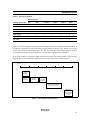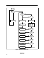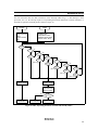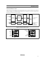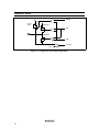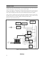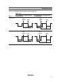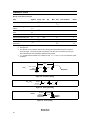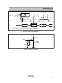
1
To all our customers Regarding the change of names mentioned in the document, such as Hitachi Electric and Hitachi XX, to Renesas Technology Corp. The semiconductor operations of Mitsubishi Electric and Hitachi were transferred to Renesas Technology Corporation on April 1st 2003. These operations include microcomputer, logic, analog and discrete devices, and memory chips other than DRAMs (flash memory, SRAMs etc.) Accordingly, although Hitachi, Hitachi, Ltd., Hitachi Semiconductors, and other Hitachi brand names are mentioned in the document, these names have in fact all been changed to Renesas Technology Corp. Thank you for your understanding. Except for our corporate trademark, logo and corporate statement, no changes whatsoever have been made to the contents of the document, and these changes do not constitute any alteration to the contents of the document itself. Renesas Technology Home Page: http://www.renesas.com Renesas Technology Corp. Customer Support Dept. April 1, 2003 Cautions Keep safety first in your circuit designs! 1. Renesas Technology Corporation puts the maximum effort into making semiconductor products better and more reliable, but there is always the possibility that trouble may occur with them. Trouble with semiconductors may lead to personal injury, fire or property damage. Remember to give due consideration to safety when making your circuit designs, with appropriate measures such as (i) placement of substitutive, auxiliary circuits, (ii) use of nonflammable material or (iii) prevention against any malfunction or mishap. Notes regarding these materials 1. These materials are intended as a reference to assist our customers in the selection of the Renesas Technology Corporation product best suited to the customer's application; they do not convey any license under any intellectual property rights, or any other rights, belonging to Renesas Technology Corporation or a third party. 2. Renesas Technology Corporation assumes no responsibility for any damage, or infringement of any third-party's rights, originating in the use of any product data, diagrams, charts, programs, algorithms, or circuit application examples contained in these materials. 3. All information contained in these materials, including product data, diagrams, charts, programs and algorithms represents information on products at the time of publication of these materials, and are subject to change by Renesas Technology Corporation without notice due to product improvements or other reasons. It is therefore recommended that customers contact Renesas Technology Corporation or an authorized Renesas Technology Corporation product distributor for the latest product information before purchasing a product listed herein. The information described here may contain technical inaccuracies or typographical errors. Renesas Technology Corporation assumes no responsibility for any damage, liability, or other loss rising from these inaccuracies or errors. Please also pay attention to information published by Renesas Technology Corporation by various means, including the Renesas Technology Corporation Semiconductor home page (http://www.renesas.com). 4. When using any or all of the information contained in these materials, including product data, diagrams, charts, programs, and algorithms, please be sure to evaluate all information as a total system before making a final decision on the applicability of the information and products. Renesas Technology Corporation assumes no responsibility for any damage, liability or other loss resulting from the information contained herein. 5. Renesas Technology Corporation semiconductors are not designed or manufactured for use in a device or system that is used under circumstances in which human life is potentially at stake. Please contact Renesas Technology Corporation or an authorized Renesas Technology Corporation product distributor when considering the use of a product contained herein for any specific purposes, such as apparatus or systems for transportation, vehicular, medical, aerospace, nuclear, or undersea repeater use. 6. The prior written approval of Renesas Technology Corporation is necessary to reprint or reproduce in whole or in part these materials. 7. If these products or technologies are subject to the Japanese export control restrictions, they must be exported under a license from the Japanese government and cannot be imported into a country other than the approved destination. Any diversion or reexport contrary to the export control laws and regulations of Japan and/or the country of destination is prohibited. 8. Please contact Renesas Technology Corporation for further details on these materials or the products contained therein. HD404818 Series 4-Bit Single-Chip Microcomputer Preliminary Rev. 2.0 Sept. 1998 Description T he H D4 04 81 8 Se ri es of 4-bit single-chip HMCS400 series microcomputers provide high program productivity. It incorporates a large size memory, LCD controller/driver, voltage comparator, and 32-kHz watch oscillator circuit. The HD404818 Series has both standard voltage versions and low voltage versions available. The standard voltage versions operate at 4.0 V to 6.0 V (mask ROM version) and 4.0 V to 5.5 V (PROM version), while the low voltage versions operate at 2.7 V to 6.0 V (mask ROM) and 3.0 V to 5.5 V (PROM). Low voltage versions include an L in their product name. Standard voltage versions: HD404812, HD404814, HD404816, HD404818, HD4074818 Low voltage versions: HD40L4812, HD40L4814, HD40L4816, HD40L4818, HD407L4818 The HD4074818 and HD407L4818, containing PROMs, are ZTAT microcomputers which can dramatically shorten system development time and smoothly proceed from debugging to mass production. ZTAT TM : Zero Turn Around Time ZTAT is a trademark of Hitachi Ltd. Features • • • • • • • • • • 2048-word × 10-bit ROM (HD404812, HD40L4812) 4096-word × 10-bit ROM (HD404814, HD40L4814) 6144-word × 10-bit ROM (HD404816, HD40L4816) 8192-word × 10-bit ROM (HD404818, HD40L4818, HD4074818, HD407L4818) 1184-digit × 4-bit RAM 30 I/O pins, including 10 high-current output pins, all CMOS and programmable as I/O pull-up MOS LCD controller/driver (32 segments × 4 commons) Three timer/counters Clock-synchronous 8-bit serial interface Six interrupt sources Two by external sources Four by internal sources HD404818 Series • Subroutine stack up to 16 levels, including interrupts • Instruction cycle time: 1 µs (fOSC = 4 MHz for HD404812/HD404814/HD404816/HD404818/HD4074818) 5 µs (fOSC = 800 kHz for HD40L4812/HD40L4814/HD40L4816/HD40L4818/HD407L4818) • Four low-power dissipation modes Standby mode Stop mode Watch mode Subactive mode • Internal oscillator: Main clock: Can be driven by ceramic oscillator, crystal oscillator, or external clock Subclock: 32.768-kHz crystal • Voltage comparator (2 channels) • Package 80-pin plastic flat package (FP-80B, FP-80A) 80-pin plastic thin flat package (TFP-80) 2 HD404818 Series Ordering Information Type Mask ROM Supply Voltage Product Name Model Name ROM (Word) Clock Frequency Package Standard (4.0 to 6.0 V) HD404812 HD404812FS 2,048 4 FP-80B HD404814 HD404816 HD404818 Low-voltage operation HD40L4812 (2.7 to 6.0 V) HD40L4814 HD40L4816 HD40L4818 ZTAT Standard (4.0 to 5.5 V) Low-voltage operation (3.0 to 5.5 V) HD4074818 HD404812H FP-80A HD404812TF TFP-80 HD404814FS 4,096 FP-80B HD404814H FP-80A HD404814TF TFP-80 HD404816FS 6,144 FP-80B HD404816H FP-80A HD404816TF TFP-80 HD404818FS 8,192 FP-80B HD404818H FP-80A HD404818TF TFP-80 HD40L4812FS 2,048 0.8 FP-80B HD40L4812H FP-80A HD40L4812TF TFP-80 HD40L4814FS 4,096 FP-80B HD40L4814H FP-80A HD40L4814TF TFP-80 HD40L4816FS 6,144 FP-80B HD40L4816H FP-80A HD40L4816TF TFP-80 HD40L4818FS 8,192 FP-80B HD40L4818H FP-80A HD40L4818TF TFP-80 HD4074818FS 8,192 4 FP-80B HD4074818H FP-80A HD4074818TF TFP-80 HD407L4818 HD407L4818FS 0.8 FP-80B HD407L4818H FP-80A HD407L4818TF TFP-80 3 HD404818 Series 4 61 62 63 64 65 66 60 2 59 3 58 4 57 5 56 6 55 7 54 8 53 9 10 52 51 TFP-80 FP-80A 11 50 40 39 38 37 36 35 34 33 32 41 30 31 43 42 20 29 44 18 19 28 45 17 27 46 16 26 47 15 25 48 14 24 49 13 23 12 (top view) (top view) 67 68 69 71 70 72 73 74 75 76 77 78 79 80 1 22 D4 D5 D6 D7 D8 D9 D10 VCref /D11 COMP0/D12 COMP1/D13 TEST X1 X2 GND SCK/R0 0 SI/R0 1 SO/R0 2 R0 3 R1 0 R1 1 21 SEG32 SEG31 SEG30 SEG29 SEG28 SEG27 SEG26 SEG25 SEG24 SEG23 SEG22 SEG21 SEG20 SEG19 SEG18 SEG17 SEG16 SEG15 SEG14 SEG13 SEG12 SEG11 SEG10 SEG9 R1 2 R1 3 R2 0 R2 1 R2 2 R2 3 R3 0 TIMO/R31 INT0 /R32 INT1 /R33 SEG1 SEG2 SEG3 SEG4 SEG5 SEG6 SEG7 SEG8 SEG9 SEG10 FP-80B 64 63 62 61 60 59 58 57 56 55 54 53 52 51 50 49 48 47 46 45 44 43 42 41 25 26 27 28 29 30 31 32 33 34 35 36 37 38 39 40 1 2 3 4 5 6 7 8 9 10 11 12 13 14 15 16 17 18 19 20 21 22 23 24 R2 0 R2 1 R2 2 R2 3 R3 0 TIMO/R3 1 INT0 /R3 2 INT1 /R3 3 SEG1 SEG2 SEG3 SEG4 SEG5 SEG6 SEG7 SEG8 D2 D3 D4 D5 D6 D7 D8 D9 D10 VC ref /D11 COMP0/D12 COMP1/D13 TEST X1 X2 GND SCK/R0 0 SI/R01 SO/R02 R03 R10 R11 R12 R13 D3 D2 D1 D0 RESET OSC2 OSC1 VCC NUMG NUMO NUMO V3 V2 V1 COM4 COM3 COM2 COM1 SEG32 SEG31 80 79 78 77 76 75 74 73 72 71 70 69 68 67 66 65 D1 D0 RESET OSC2 OSC1 VCC NUMG NUMO NUMO V3 V2 V1 COM4 COM3 COM2 COM1 Pin Arrangement SEG30 SEG29 SEG28 SEG27 SEG26 SEG25 SEG24 SEG23 SEG22 SEG21 SEG20 SEG19 SEG18 SEG17 SEG16 SEG15 SEG14 SEG13 SEG12 SEG11 HD404818 Series Pin Description Pin Number Pin Number FP-80B FP-80A, TFP-80 Pin Name I/O FP-80B FP-80A, TFP-80 Pin Name I/O 1 79 D2 I/O 31 29 R3 2/INT0 I/O 2 80 D3 I/O 32 30 R3 3/INT1 I/O 3 1 D4 I/O 33 31 SEG1 O 4 2 D5 I/O 34 32 SEG2 O 5 3 D6 I/O 35 33 SEG3 O 6 4 D7 I/O 36 34 SEG4 O 7 5 D8 I/O 37 35 SEG5 O 8 6 D9 I/O 38 36 SEG6 O 9 7 D10 I 39 37 SEG7 O 10 8 D11/VCref I 40 38 SEG8 O 11 9 D12/COMP0 I 41 39 SEG9 O 12 10 D13/COMP1 I 42 40 SEG10 O 13 11 TEST I 43 41 SEG11 O 14 12 X1 I 44 42 SEG12 O 15 13 X2 O 45 43 SEG13 O 16 14 GND 46 44 SEG14 O 17 15 R0 0/SCK I/O 47 45 SEG15 O 18 16 R0 1/SI I/O 48 46 SEG16 O 19 17 R0 2/SO I/O 49 47 SEG17 O 20 18 R0 3 I/O 50 48 SEG18 O 21 19 R1 0 I/O 51 49 SEG19 O 22 20 R1 1 I/O 52 50 SEG20 O 23 21 R1 2 I/O 53 51 SEG21 O 24 22 R1 3 I/O 54 52 SEG22 O 25 23 R2 0 I/O 55 53 SEG23 O 26 24 R2 1 I/O 56 54 SEG24 O 27 25 R2 2 I/O 57 55 SEG25 O 28 26 R2 3 I/O 58 56 SEG26 O 29 27 R3 0 I/O 59 57 SEG27 O 30 28 R3 1/TIMO I/O 60 58 SEG28 O 5 HD404818 Series Pin Number Pin Number FP-80B FP-80A, TFP-80 Pin Name I/O FP-80B FP-80A, TFP-80 Pin Name I/O 61 59 SEG29 O 71 69 V3 62 60 SEG30 O 72 70 NUMO 63 61 SEG31 O 73 71 NUMO 64 62 SEG32 O 74 72 NUMG 65 63 COM1 O 75 73 VCC 66 64 COM2 O 76 74 OSC 1 I 67 65 COM3 O 77 75 OSC 2 O 68 66 COM4 O 78 76 RESET I 69 67 V1 79 77 D0 I/O 70 68 V2 80 78 D1 I/O Note: I/O: Input/output pin, I: Input pin, O: Output pin, NUMO: Open, NUMG: GND 6 HD404818 Series Pin Functions Power Supply VCC: Apply the VCC power supply voltage to this pin. GND: Connect to ground. TEST: For test purposes only. Connect it to VCC. RESET: MCU reset pin. Refer to the Reset section for details. NUMG: Non-user pin. Connect it to GND. NUMO: Non-user pin. Do not connect it to any lines. Oscillators OSC 1, OSC2: Internal oscillator input pins. They both can be connected to a crystal, ceramic resonator, or external oscillator circuit. Refer to the Internal Oscillator Circuit section for details. X1, X2: Watch oscillator 32-kHz crystal pins. Ports D0–D13 (D Port): Fourteen 1-bit I/O ports. D0 to D9 are I/O ports and D 10 to D13 are input ports. D0–D9 are high current output ports (15 mA max.). D11–D13 are also available as voltage comparators. Refer to the Input/Output section for details. R0–R3 (R Ports): 4-bit I/O ports. R00, R01, R02, R31, R32, and R33 are multiplexed with SCK, SI, SO, TIMO, INT 0, and INT 1, respectively. Interrupts INT0, INT1: External interrupt pins. INT1 can be used as an external event input pin for timer B. INT0 and INT 1 are multiplexed with R32 and R33, respectively. For details, see the Interrupts section. Serial Interface SCK, SI, SO: The transmit clock I/O pin (SCK), serial data input pin (SI), and serial data output pin (SO) are used for serial interface. SCK, SI, and SO are multiplexed with R00, R01, and R0 2, respectively. For details, see the Serial Interface section. Timer TIMO: Variable duty-cycle pulse waveform output pin. See the Timer C section for details. 7 HD404818 Series LCD Driver/Controller V1, V2, V3: Power supply pins for the LCD driver. Since the LCD driving resistors are provided internally, no lines should be connected to these pins. The voltage on each pin is VCC ≥ V 1 ≥ V2 ≥ V3 ≥ GND. See the Liquid Crystal Display section for details. COM1 to COM4: Common signal output pins for the LCD display. See the Liquid Crystal Display section for details. SEG1 to SEG32: Segment signals output pins for the LCD display. See the Liquid Crystal Display section for details. Voltage Comparator COMP 0, COMP 1, VCref: Analog input pins for the voltage comparator. VCref is used as a reference voltage pin to input the threshold voltage of the analog input pin. 8 HD404818 Series VCC GND OSC 1 OSC 2 X1 X2 RESET TEST Block Diagram D port D0 D1 D2 D3 D4 D5 D6 D7 D8 D9 D10 D11 D12 D13 R0 port R00 R01 R02 R03 R1 port External interrupt control circuit R10 R11 R12 R13 R2 port INT0 INT1 R20 R21 R22 R23 R3 port System control circuit R30 R31 R32 R33 RAM (1,184 × 4 bits) W (2 bits) Timer A X (4 bits) Timer B VCref COMP0 COMP1 SPY (4 bits) ALU CPU Comparator Internal data bus Serial interface Internal address bus SI SO SCK Y (4 bits) Timer C Internal data bus TIMO SPX (4 bits) Highcurrent pins CA ST (1 bit) (1 bit) A (4 bits) V1 V2 V3 COM1 COM2 COM3 COM4 SEG1 SEG2 SEG3 SEG31 SEG32 B (4 bits) LCD driver circuit SP (10 bits) Instruction decoder PC (14 bits) ROM (2,048 × 10 bits) (4,096 × 10 bits) (6,144 × 10 bits) (8,192 × 10 bits) : Data bus : Signal lines 9 HD404818 Series Memory Map ROM Memory Map The ROM is described in the following paragraphs with the ROM memory map in figure 1. 0 $0000 Vector address 15 $000F 16 $0010 Zero-page subroutine (64 words) $003F 63 64 $0040 Pattern (4096 words) 4095 $0FFF 4096 $1000 Program * 8191 $1FFF 8192 $2000 Not used 16383 0 1 2 3 JMPL instruction (jump to reset routine) 4 5 6 7 8 9 JMPL instruction (jump to INT1 routine) 10 11 12 13 14 15 JMPL instruction (jump to INT0 routine) JMPL instruction (jump to timer A routine) JMPL instruction (jump to timer B routine) JMPL instruction (jump to timer C routine) JMPL instruction (jump to serial routine) $0000 $0001 $0002 $0003 $0004 $0005 $0006 $0007 $0008 $0009 $000A $000B $000C $000D $000E $000F Note: * HD404812, HD40L4812: 2048 words HD404814, HD40L4814: 4096 words HD404816, HD40L4816: 6144 words HD404818, HD40L4818, HD4074818, HD407L4818: 8192 words $3FFF Figure 1 ROM Memory Map Vector Address Area ($0000 to $000F): Locations $0000 through $000F are reserved for JMPL instructions to branch to the starting address of the initialization program and of the interrupt programs. After reset or an interrupt routine, the program is executed from the vector address. Zero-Page Subroutine Area ($0000 to $003F): Locations $0000 through $003F are reserved for subroutines. The program sequence branches to subroutines by the CAL instruction. Pattern Area ($0000 to $0FFF): Locations $0000 through $0FFF are reserved for ROM data. The P instruction allows the MCU to reference ROM data as a pattern. Program Area ($0000 to $07FF: HD404812, HD40L4812; $0000 to $0FFF: HD404814, HD40L4814; $0000 to $17FF: HD404816, HD40L4816; $0000 to $1FFF: HD404818, HD40L4818, HD4074818, HD407L4818): Used for program coding. 10 HD404818 Series RAM Memory Map The MCU also contains a 1,184-digit × 4-bit RAM as the data and stack area. In addition to these areas, interrupt control bits and special function registers are mapped on the RAM memory space. The RAM memory map (figure 2) is described in the following paragraphs. Interrupt Control Bits Area ($000 to $003): The interrupt control bits area (figure 3) is used for interrupt control. It is accessible only by RAM bit manipulation instructions. However, the interrupt request flag cannot be set by software. The RSP bit is used only to reset the stack pointer. Special Function Registers Area ($004 to $01F, $024 to $03F): The special function registers are the mode or data registers for the serial interface, timer/counters, LCD, and the data control registers for the I/O ports. These registers are classified into three types: write-only, read-only, and read/write as shown in figure 2. The SEM/REM and SEMD/REMD instructions are available for the LCD control register (LCR). Other registers cannot be accessed by RAM bit manipulation instructions. Register Flag Area ($020 to $023): Consist of the LSON, WDON, TGSP, and DTON flags which are bit registers accessible by the RAM bit manip ula tion instruction. The WDON flag can only be set, and only by the SEM/SEMD instruction. The DTON flag can be set, reset, and tested by the SEM/SEMD, REM/REMD, and TMD instructions. Note that the DTON flag is active only in subactive mode, and is normally reset in active mode. LCD Data Area ($050 to $06F): Locations $050 to $06F store the LCD data which is automatically transmitted to the segment driver as display data. The LCD is illuminated with 1s and faded with 0s. This area can be used as a data area. Data Area ($040 to $2CF, $100 to $2CF; Bank 0/1): The 16 digits of $040 through $04F are called memory registers (MR) and are accessible by the LAMR and XMRA instructions (figure 4). 464 digits of $100 through $2CF are selected as bank 0 or 1 depending on the value of the V register. Stack Area ($3C0 to $3FF): Locations $3C0 through $3FF are reserved for LIFO stacks to save the contents of the program counter (PC), status flag (ST), and carry flag (CA) when subroutine calls (CAL or CALL instruction) and interrupts are processed. This area can be used as a 16-level nesting stack in which one level requires 4 digits. Figure 4 shows the save condition. The program counter is restored by the RTN and RTNI instructions. The status and carry flags are restored only by the RTNI instruction. This area, when not used as a stack, is available as a data area. 11 HD404818 Series 0 $000 RAM-mapped registers 63 64 80 112 Memory registers (MR) LCD display area (32 digits) $03F $040 $050 $070 Data (144 digits) $100 Data (464 digits × 2) V = 0 (bank 0) V = 1 (bank 1) 0 1 2 3 4 5 6 7 8 9 10 11 $2CF 12 13 14 Interrupt control bits area Port mode register A Serial mode register $3BF 959 960 $3C0 Stack (64 digits) $3FF 1023 16 17 18 19 20 W W Serial data register lower (SRL) R/W Serial data register upper (SRU) R/W Timer mode register A (TMA) W Timer mode register B (TMB) W Timer B (TCBL/TLRL) (TCBU/TLRU) Miscellaneous register (MIS) Timer mode register C (TMC) Timer C (TCCL/TCRL) (TCCU/TCRU) 15 Not used (PMRA) (SMR) Not used Not used Port mode register B (PMRB) LCD control register LCD mode register Not used 32 (LCR) (LMR) $000 $001 $002 $003 $004 $005 $006 $007 $008 $009 R/W R/W $00A $00B W W $00C R/W R/W $00E $00F $010 $00D $011 W W W $012 $013 $014 $020 Register flag area $023 35 Not used The data area has two banks: bank 0 (V = 0) and bank 1 (V = 1) $100 Data (464 digits) V = 1 (bank 1) 48 49 50 51 Port R0 DCR Port R1 DCR (DCR0) (DCR1) Port R2 DCR Port R3 DCR (DCR2) (DCR3) Data (464 digits) V = 0 (bank 0) W $030 $031 W W W $032 $033 Not used $2CF Note: Do not use any area labelled "Not used". R: Read only W: Write only R/W: Read/write 59 60 61 Port D0 –D 3 DCR (DCRB) Port D4 –D 7 DCR (DCRC) 63 V register Port D8 –D 9 DCR (DCRD) Not used $03B $03C $03D R/W $03F 10 Timer counter B lower (TCBL) R Timer load register B lower (TLRL) W $00A 11 Timer counter B upper (TCBU) R Timer load register B upper (TLRU) W 14 Timer counter C lower (TCCL) R Timer load register C lower (TCRL) W $00E 15 Timer counter C upper (TCCU) R Timer load register C upper (TCRU) W $00F Figure 2 RAM Memory Map (1,184-digit × 4-bit) 12 (V-REG) W W W $00B HD404818 Series Bit 3 Bit 2 Bit 1 Bit 0 0 IM0 (IM of INT0 ) IF0 (IF of INT0 ) RSP (Reset SP bit) 1 IMTA (IM of timer A) IFTA (IF of timer A) IM1 (IM of INT1 ) IF1 (IF of INT1 ) $001 2 IMTC (IM of timer C) IFTC (IF of timer C) IMTB (IM of timer B) IFTB (IF of timer B) $002 3 Not used Not used IMS (IM of serial) IFS (IF of serial) $003 32 DTON Direct transfer on flag Not used WDON (Watchdog on flag) LSON (Low speed on flag) $020 IE (Interrupt enable flag) $000 $021 Not used $023 IF: Interrupt request flag IM: Interrupt mask IE: Interrupt enable flag SP: Stack pointer Note: Bits in the interrupt control bits area and register flag area are set by the SEM or SEMD instruction, reset by the REM or REMD instruction, and tested by the TM or TMD instruction. Other instructions have no effect. However, note the following usage limitations of RAM bit manipulation instructions. SEM/SEMD REM/REMD TM/TMD IF Not executed Allowed Allowed RSP Not executed Allowed Inhibited WDON Allowed Not executed Inhibited DTON Not executed in active mode Allowed Allowed Used in subactive mode Note: WDON is reset only by MCU reset. DTON is always reset in active mode. If the TM or TMD instruction is executed for the inhibited bits or non-existing bits, the value in ST becomes invalid. Figure 3 Configuration of Interrupt Control Bits and Register Flag Areas 13 HD404818 Series Memory registers 64 65 66 67 68 69 MR (0) MR (1) $040 MR (2) MR (3) $042 MR (4) $044 $045 Stack area 960 $041 $043 Level 16 Level 15 Level 14 Level 13 70 $046 Level 11 Level 10 71 MR (7) $047 Level 9 72 MR (8) MR (9) $048 Level 8 73 $049 74 MR (10) $04A 75 $04B 76 MR (11) MR (12) Level 7 Level 6 Level 5 $04C Level 4 77 MR (13) $04D Level 3 78 MR (14) MR (15) $04E Level 2 Level 1 $04F 1023 PC13 to PC0 : Program counter ST: Status flag CA: Carry flag Level 12 MR (5) MR (6) 79 $3C0 $3FF Bit 3 Bit 2 Bit 1 Bit 0 1020 ST PC13 PC12 PC11 $3FC 1021 PC10 PC 9 PC 8 PC 7 $3FD 1022 CA PC 6 PC 5 PC 4 $3FE 1023 PC 3 PC 2 PC 1 PC 0 $3FF Figure 4 Configuration of Memory Registers, Stack Area, and Stack Position 14 HD404818 Series Functional Description Registers and Flags The MCU provides ten registers and two flags for CPU operations. They are illustrated in figure 5 and described in the following paragraphs. 3 Accumulator 0 (A) Initial value: Undefined, R/W 3 B register Initial value: Undefined, R/W 0 (B) 0 V register Initial value: 0, R/W (V) 1 W register Initial value: Undefined, R/W 0 (W) 3 X register Initial value: Undefined, R/W 0 (X) 3 Y register Initial value: Undefined, R/W SPX register Initial value: Undefined, R/W SPY register Initial value: Undefined, R/W Carry Initial value: Undefined, R/W Status Initial value: 1, no R/W 0 (Y) 3 0 (SPX) 3 0 (SPY) 0 (CA) 0 (ST) 13 Program counter Initial value: 0, no R/W 0 (PC) 9 Stack pointer Initial value: $3FF, no R/W 1 5 1 1 1 0 (SP) Figure 5 Registers and Flags Accumulator (A), B Register (B): The accumulator and B register are 4-bit registers which hold the results of the arithmetic logic unit (ALU), and exchange data between memory, I/O, and other registers. 15 HD404818 Series V Register (V): The V register, available for RAM address expansion, selects the bank of locations $100– $2CF on the RAM address (464 digits) depending on its value. Therefore, when accessing locations $100– $2CF on the RAM address, specify the value of the V register (V = $0: bank 0; V = $1: bank 1). Locations $000–$0FF and $300–$3FF can be accessed independently of the V register. The V register is located at $03F of the RAM address area. W Register (W), X Register (X), Y Register (Y): The 2-bit W register and 4-bit X and Y registers address RAM indirectly. The Y register is also available for addressing port D. SPX Register (SPX), SPY Register (SPY): The 4-bit SPX and SPY registers are available for assisting the X and Y registers, respectively. Carry Flag (CA): The carry flag holds the ALU overflow generated by an arithmetic operation. It is also affected by the SEC, REC, ROTL, and ROTR instructions. During an interrupt, the carry flag is pushed onto the stack and restored back from the stack by the RTNI instruction. (It is unaffected by the RTN instruction.) Status Flag (ST): The status flag holds the ALU overflow, ALU non-zero, and the results of a bit test instruction for arithmetic or compare instructions. The status flag is a branch condition of the BR, BRL, CAL, or CALL instruction. The value of the status flag remains unchanged until an instruction which affects the next status is executed. The status flag becomes 1 after the BR, BRL, CAL, or CALL instruction is either executed or skipped. During an interrupt, the status flag is pushed onto the stack and restored back from the stack by the RTNI instruction, not by the RTN instruction. Program Counter (PC): The program counter is a 14-bit binary counter for holding the ROM address. Stack Pointer (SP): The stack pointer is a 10-bit register to indicate the next stacking area up to 16 levels. The stack pointer is initialized to RAM address $3FF at MCU reset. It is decremented by 4 as data is pushed onto the stack, and incremented by 4 as data is restored back from the stack. The stack pointer is initialized to $3FF either by MCU reset or by the RSP bit reset from the REM/REMD instruction. 16 HD404818 Series Reset Setting the RESET pin high resets the MCU. At power-on or when cancelling the stop mode for the oscillator, apply the reset input for at least t RC for the oscillator to stabilize. In all other cases, at least two instruction cycles of reset input are required for the MCU reset. Table 1 shows the components initialized by MCU reset, and each of its status. Table 1 Initial Values after MCU Reset Items Initial Value Contents Program counter (PC) $0000 Execute program from the top of the ROM address Status flag (ST) 1 Enable branching with conditional branch instructions Stack pointer (SP) $3FF Stack level is 0 V register (bank register) (V) 0 Bank 0 (memory) Interrupt flags/mask Interrupt enable flag (IE) 0 Inhibit all interrupts Interrupt request flag (IF) 0 No interrupt request Interrupt mask (IM) 1 Masks interrupt request Port data register (PDR) All bits are 1 Enable to transmit high Data control register (DCR) All bits are 0 Output buffer is off (high impedance) Port mode register A (PMRA) 0000 See Port Mode Register A section Port mode register B (PMRB) 0000 See Port Mode Register B section Timer mode register A (TMA) 0000 See Timer Mode Register A section Timer mode register B (TMB) 0000 See Timer Mode Register B section Timer mode register C (TMC) 0000 See Timer Mode Register C section Serial mode register (SMR) 0000 See Serial Mode Register section Prescaler S $000 Prescaler W $00 Timer counter A (TCA) $00 Timer counter B (TCB) $00 Timer counter C (TCC) $00 Timer load register B (TLR) $00 Timer load register C (TCR) $00 Octal counter 000 I/O Timer/counters, serial interface 17 HD404818 Series Table 1 Initial Values after MCU Reset (cont) Items LCD Bit register Miscellaneous register Initial Value Contents LCD control register (LCR) 000 Refer to description of LCD Control Register LCD mode register (LMR) 0000 Refer to description of LCD Duty/Clock Control Low speed on flag (LSON) 0 Refer to description of Low-Power Dissipation Mode Watchdog timer on flag (WDON) 0 Refer to description of Timer C Direct transfer on flag (DTON) 0 Refer to description of Low-Power Dissipation Mode (MIS) — Item Carry flag (CA) 000 After MCU Reset to Recover from Stop Mode After MCU Reset to Recover from Other Modes The contents of the items before MCU reset are not retained. It is necessary to initialize them by software. The contents of the items before MCU reset are not retained. It is necessary to initialize them by software. Accumulator (A) B register (B) W register (W) X/SPX registers (X/SPX) Y/SPY registers (Y/SPY) Serial data register (SR) RAM 18 The contents of RAM before MCU reset (just before STOP instruction) are retained. HD404818 Series Interrupts Six interrupt sources are available on the MCU: external requests (INT0, INT1), timer/counters (timers A, B, and C), and the serial interface. For each source, an interrupt request flag (IF), interrupt mask (IM), and interrupt vector addresses are provided to control and maintain the interrupt request. The interrupt enable flag (IE) is also used to control interrupt operations. Interrupt Control Bits and Interrupt Servicing: The interrupt control bits are mapped on $000 through $003 by the RAM space. They are accessible by RAM bit manipulations instructions, although the interrupt request flag (IF) cannot be set by software. The interrupt enable flag (IE) and IF are cleared to 0, and the interrupt mask (IM) is set to 1 after MCU reset. Figure 6 is a block diagram of the interrupt control circuit. Table 2 shows the interrupt priority and vector addresses, and table 3 shows the interrupt conditions corresponding to each interrupt source. The interrupt request is generated when IF is set to 1 and IM is 0. If IE is 1 at this time, the interrupt will be activated and vector addresses will be generated from the priority PLA corresponding to the interrupt sources. 19 HD404818 Series $ 000,0 Sequence control • Push PC/CA/ST • Reset IE • Jump to vector address IE $ 000,2 IF0 $ 000,3 IM0 Vector address Priority control logic $ 001,0 IF1 $ 001,1 IM1 $ 001,2 IFTA $ 001,3 IMTA $ 002,0 IFTB $ 002,1 IMTB $ 002,2 IFTC $ 002,3 IMTC $ 003,0 IFS $ 003,1 IMS Note: $m, n is RAM address $m, bit number n. Figure 6 Interrupt Control Circuit Block Diagram Table 2 Vector Addresses and Interrupt Priority Reset/Interrupt Priority Vector Addresses RESET — $0000 INT0 1 $0002 INT1 2 $0004 Timer A 3 $0006 Timer B 4 $0008 Timer C 5 $000A Serial 6 $000C 20 HD404818 Series Table 3 Interrupt Conditions Interrupt Source Interrupt Control Bit INT0 INT1 Timer A Timer B Timer C Serial IE 1 1 1 1 1 1 IF0 • IM0 1 0 0 0 0 0 IF1 • IM1 * 1 0 0 0 0 IFTA • IMTA * * 1 0 0 0 IFTB • IMTB * * * 1 0 0 IFTC • IMTC * * * * 1 0 IFS • IMS * * * * * 1 Note: *Don’t care. Figure 7 shows the interrupt processing sequence, and figure 8 shows the interrupt processing flowchart. If an interrupt is requested, the instruction being executed finishes in the first cycle. The IE is reset in the second cycle. In the second and third cycles, the carry flag, status flag, and program counter are pushed onto the stack. In the third cycle, the instruction is executed after jumping to the vector address. In each vector address, program the JMPL instruction to branch to the starting address of the interrupt program. The IF, which caused the interrupt, must be reset by software in the interrupt program. Instruction cycles 1 2 3 4 5 6 Instruction execution Interrupt acceptance Stacking; reset of IE Stacking; vector address generated JMPL instruction execution on the vector address Instruction execution at starting address of the interrupt routine Figure 7 Interrupt Processing Sequence 21 HD404818 Series Power on RESET = 1 ? Yes No Interrupt request ? Yes No No IE = 1? Yes Reset MCU Accept interrupt Execute instruction IE ←0 Stack ← (PC) Stack ← (CA) Stack ← (ST) PC ←(PC) + 1 PC← $0002 Yes INT0 interrupt ? No PC← $0004 Yes INT1 interrupt ? No PC← $0006 Yes Timer A interrupt ? No PC← $0008 Yes Timer B interrupt ? No PC ← $000A Yes Timer C interrupt ? No PC ← $000C Figure 8 Interrupt Processing Flowchart 22 (serial interrupt) HD404818 Series Interrupt Enable Flag (IE: $000, Bit 0): The interrupt enable flag enables/disables interrupt requests (table 4). It is reset by an interrupt and set by the RTNI instruction. Table 4 Interrupt Enable Flag IE Interrupt Enabled/Disabled 0 Disabled 1 Enabled External Interrupts (INT0, INT1): The external interrupt request inputs (INT0, INT1) can be selected by port mode register A (PMRA: $004). The external interrupt request flags (IF0, IF1) are set at the falling edge of INT0 and INT1 inputs, respectively (table 5). The INT1 input can be used as a clock signal input to timer B, in which timer B counts up at each falling edge of the INT1 input. When using INT1 as the timer B external event input, the external interrupt mask (IM1) has to be set so that the interrupt request by INT1 will not be accepted (table 6). More than two instruction cycle times (2t cyc/2tsubcyc ) are needed to detect the edge of INT 0 or INT1. External Interrupt Request Flags (IF0: $000, Bit 2; IF1: $001, Bit 0): The external interrupt request flags (IF0, IF1) are set at the falling edge of the INT0 and INT1 inputs, respectively (table 5). Table 5 External Interrupt Request Flags IF0, IF1 Interrupt Request 0 No 1 Yes External Interrupt Masks (IM0: $000, Bit 3; IM1: $001, Bit 1): The external interrupt masks mask the external interrupt requests (table 6). Table 6 External Interrupt Masks IM0, IM1 Interrupt Request 0 Enabled 1 Disabled (masked) Timer A Interrupt Request Flag (IFTA: $001, Bit 2): The timer A interrupt request flag is set by the overflow output of timer A (table 7). 23 HD404818 Series Table 7 Timer A Interrupt Request Flag IFTA Interrupt Request 0 No 1 Yes Timer A Interrupt Mask (IMTA: $001, Bit 3): The timer A interrupt mask prevents an interrupt request from being generated by the timer A interrupt request flag (table 8). Table 8 Timer A Interrupt Mask IMTA Interrupt Request 0 Enabled 1 Disabled (masked) Timer B Interrupt Request Flag (IFTB: $002, Bit 0): The timer B interrupt request flag is set by the overflow output of timer B (table 9). Table 9 Timer B Interrupt Request Flag IFTB Interrupt Request 0 No 1 Yes Timer B Interrupt Mask (IMTB: $002, Bit 1): The timer B interrupt mask prevents an interrupt request from being generated by the timer B interrupt request flag (table 10). Table 10 Timer B Interrupt Mask IMTB Interrupt Request 0 Enabled 1 Disabled (masked) Timer C Interrupt Request Flag (IFTC: $002, Bit 2): The timer C interrupt request flag is set by the overflow output of timer C (table 11). Table 11 Timer C Interrupt Request Flag IFTC Interrupt Request 0 No 1 Yes 24 HD404818 Series Timer C Interrupt Mask (IMTC: $002, Bit 3): The timer C interrupt mask prevents the interrupt from being generated by the timer C interrupt request flag (table 12). Table 12 Timer C Interrupt Mask IMTC Interrupt Request 0 Enabled 1 Disabled (masked) Serial Interrupt Request Flag (IFS: $003, Bit 0): The serial interrupt request flag is set when the octal counter counts eight transmit clock signals, or when data transfer is discontinued by resetting the octal counter (table 13). Table 13 Serial Interrupt Request Flag IFS Interrupt Request 0 No 1 Yes Serial Interrupt Mask (IMS: $003, Bit 1): The serial interrupt mask masks the interrupt request (table 14). Table 14 Serial Interrupt Mask IMS Interrupt Request 0 Enabled 1 Disabled (masked) 25 HD404818 Series Operating Modes The MCU has five operating modes that are specified by how the clock is used. The functions available in each mode are listed in table 15, and operations are shown in table 16. Transitions between operating modes are shown in figure 9. Table 16 provides additional information for table 26. Table 15 Functions Available in Each Operating Mode Mode Name Active Standby Stop Watch Subactive*4 Activation method RESET cancellation, interrupt request SBY instruction TMA3 = 0, STOP instruction TMA3 = 1, STOP instruction INT0 or timer A interrupt request from watch mode Status OP OP Stopped Stopped Stopped OP OP System oscillator 1 Subsystem oscillator OP OP OP * Instruction execution OP (øCPU) Stopped Stopped Stopped OP Peripheral function, interrupt (øPER) OP OP Stopped Stopped OP Clock function, interrupt (øCLK) OP OP Stopped OP *2 OP *2 RAM OP Retained Retained Retained OP Registers/flags OP Retained Reset Retained I/O Cancellation method OP Retained High impedance*3 RESET input, RESET input, RESET input STOP/SBY interrupt instruction request OP 3 Retained* OP *3 RESET input, RESET input, INT0 or timer A STOP/SBY instruction interrupt request Notes: OP indicates operating. 1. To reduce current dissipation, stop all oscillation in external circuits. 2. Refer to the Interrupt Frame section for details. 3. Refer to interrupt frame. 4. Subactive mode is an optional function to be specified on the function option list. 5. In the watch and subactive modes, the MCU requires a 32.768-kHz crystal oscillator. 26 HD404818 Series Table 16 Operations in Low-Power Dissipation Modes Function Stop Mode Watch Mode Standby Mode Subactive Mode*2 CPU Reset Retained Retained OP RAM Retained Retained Retained OP Timer A Reset OP OP OP Timer B Reset Stopped OP OP Timer C Reset Stopped OP OP Stopped* OP OP OP OP OP Retained Retained OP Serial interface Reset LCD Reset 3 1 I/O Reset* Notes: OP indicates operating. 1. Output pins are at high impedance. 2. Subactive mode is an optional function to be specified on the function option list. 3. Transmission/reception is activated if a clock is input in external clock mode. (However, interrupts are stopped.) Table 17 I/O Status in Low-Power Dissipation Modes Output Input Standby Mode, Watch Mode Stop Mode Active Mode, Subactive Mode D0–D 9 Retained High impedance Input enabled D10–D 13 — — Input enabled R0–R3 Retained High impedance Input enabled System Clock (øCPU) Non-time-base peripheral function clock (øPER) Operating Operating Stopped Active mode Standby mode Subactive mode Stopped — Watch mode (TMA3 = 1) Stop mode (TMA3 = 0) 27 HD404818 Series Reset Standby mode Active mode Stop mode (TMA3 = 0) f OSC : fX: ø CPU: ø CLK: ø PER: Operating Operating Stopped f cyc f cyc SBY (standby) Interrupt Timers A, B, C Serial, INT0 , INT 1 f OSC : fX: ø CPU: ø CLK: ø PER: (TMA3 = 0) Operating Operating f cyc f cyc f cyc STOP f OSC : fX: ø CPU: ø CLK: ø PER: Stopped Operating Stopped Stopped Stopped Watch mode (TMA3 = 1) f OSC : fX: ø CPU: ø CLK: ø PER: f OSC : fX: f cyc : f SUB : ø CPU : ø CLK : ø PER : LSON: DTON: Operating Operating Stopped f SUB f cyc SBY (standby) Interrupt Timers A, B, C Serial, INT0 , INT 1 Main oscillation frequency Suboscillation frequency for time-base f OSC /4 f X /8 System clock Clock for time-base Clock for other peripheral functions Low speed on flag Direct transfer on flag f OSC : fX: ø CPU: ø CLK: ø PER: (TMA3 = 1, LSON = 0) Operating Operating f cyc f SUB f cyc STOP INT0 , Timer A*1 Subactive mode Stopped Operating f SUB f SUB f SUB Notes: 1. 2. 3. 4. Stopped Operating Stopped f SUB Stopped *3 *2 f OSC : fX: ø CPU: ø CLK: ø PER: f OSC : fX: ø CPU: ø CLK: ø PER: STOP INT0 , Timer A* 1 STOP/SBY (LSON = 1)* 4 (TMA3 = 1, LSON = 1) f OSC : fX: ø CPU: ø CLK: ø PER: Stopped Operating Stopped f SUB Stopped Time-base interrupt STOP/SBY (DTON = 1, LSON = 0) STOP/SBY (DTON = 0, LSON = 0) DTON is not affected Figure 9 MCU Status Transitions Active Mode: The MCU operates according to the clock generated by the system oscillators OSC1 and OSC2. Standby Mode: The MCU enters standby mode when the SBY instruction is executed from active mode. In this mode, the oscillators, interrupts, timer/counters, and serial interface continue to operate, but all instruction execution-related clocks stop. The stopping of these clocks stops the CPU, retaining all RAM and register contents and maintaining the current I/O pin status. Standby mode is terminated by a RESET input oran interrupt request. If it is terminated by a RESET input, the MCU is reset as well. After an interrupt request, the MCU enters active mode and resumes, executing 28 HD404818 Series the next instruction after the SBY instruction. If the interrupt enable flag is 1, that interrupt is then processed; if it is 0, the interrupt request is left pending and normal instruction execution continues. A flowchart of operation in standby mode is shown in figure 10. Standby Watch Oscillator: Active Peripheral clocks: Active All other clocks: Stop Oscillator: Stop Suboscillator: Active Peripheral clocks: Stop All other clocks: Stop RESET =1? No Yes No IF0 = 1? Yes IM0 = 0? Yes No No IF1 = 1? Yes IM1 = 0? (SBY only) Yes No No IFTA = 1? Yes IMTA = 0? No Yes No IFTB = 1? Yes IMTB = No 0? (SBY only) Yes No IFTC = 1? Yes IMTC = No 0? (SBY only) Yes IFS = No 1? Yes IMS = 0? (SBY only) No Yes Restart processor clocks Restart processor clocks Execute next instruction (active mode) No IF = 1, IM = 0, and IE = 1? Yes Reset MCU Execute next instruction Accept interrupt Figure 10 MCU Operating Flowchart of Watch and Standby Modes 29 , HD404818 Series Stop Mode: The MCU enters stop mode if the STOP instruction is executed in active mode when TMA3 = 0. In this mode, the system oscillator stops, which stops all MCU functions as well. Stop mode is terminated by a RESET input as shown in figure 11. RESET must be high for at least one tRC to stabilize oscillation (refer to the AC Characteristics section). When the MCU restarts after stop mode is cancelled, all RAM contents are retained, but the accuracy of the contents of the accumulator, B register, W register, X/SPX register, Y/SPY register, carry flag, and serial data register cannot be guaranteed. Stop mode Oscillator Internal clock RESET t res STOP instruction execution t res ≥ t RC (stabilization time) Figure 11 Timing of Stop Mode Cancellation Watch Mode: The MCU enters watch mode if the STOP instruction is executed in active mode when TMA3 = 1, or if the STOP or SBY instruction is executed in subactive mode. Watch mode is terminated by a RESET input or a timer-A/INT0 interrupt request. For details on RESET input, refer to the Stop Mode section. When terminated by a timer-A/INT0 interrupt request, the MCU enters active mode if LSON is 0, or subactive mode if LSON is 1. After an interrupt request is generated, the time required to enter active mode is tRC for a timer A interrupt, and TX (where T + tRC ≤ TX ≤ 2T + tRC) for an INT0 interrupt, as shown in figure 12. Operation during mode transition is the same as that at standby mode cancellation (figure 10). 30 HD404818 Series Oscillation stabilization period Active mode Watch mode Active mode Interrupt strobe INT0 Interrupt request generation T (During the transition from watch mode to active mode only) T tRC TX T: Interrupt frame length tRC: Oscillation stabilization period Figure 12 Interrupt Frame Subactive Mode: The CPU operates with a clock generated by the X1 and X2 oscillation circuits. Functions that can operate in subactive mode are listed in table 16. When the STOP or SBY instruction is executed in subactive mode, the MCU enters either watch or active mode, depending on the statuses of LSON and DTON. The DTON flag can only be set in subactive mode; it is automatically reset after a transition to active mode. Subactive mode is an optional function that the user must specify on the function option list. Interrupt Frame: In watch and subactive modes, øCLK is supplied for timer A and the INT0 circuit. Prescaler W and timer A operate as time bases to generate interrupt frame timing. Three interrupt frame cycles (T) can be selected by the settings of the miscellaneous register, as shown in figure 13. In watch and subactive modes, timer A and INT0 interrupts are generated in synchronism with the interrupt frame. An interrupt request is generated at an interrupt strobe, except when the MCU enters active mode from watch mode. The INT0 falling edge is acknowledged regardless of the interrupt frame, but an interrupt is executed simultaneously with the second interrupt strobe. Timer A generates an overflow and interrupt request at an interrupt strobe. 31 HD404818 Series MIS: $00C MIS2 MIS MIS1 MIS0 T *1 t RC 1 Bit 0 Bit 0 0 0.24414 ms 0 1 1 0 15.625 ms 62.5 ms 1 1 t RC selection Refer to table 20 *1 0.12207 ms 0.24414 ms * 2 7.8125 ms 31.25 ms Not used Oscillation circuit condition External clock input Ceramic or crystal oscillator — Notes: 1. The value of t RC applies only when using a 32.768-kHz oscillator. 2. Only direct transfer. Figure 13 Miscellaneous Register Direct Transfer: By controlling the DTON, the MCU can be placed directly from subactive to active mode. The detailed procedure is as follows: • Set the DTON flag in subactive mode while LSON = 0. • Execute the STOP or SBY instruction. • After the oscillation stabilization time (a fixed value), the MCU will move automatically from subactive to active mode. Note that DTON ($020, bit 3) is valid only in subactive mode. When the MCU is in active mode, this flag is always at reset. The transition time (tD) from subactive to active mode is tRC < tD < T + tRC. STOP/SBY execution Internal execution time (< T) Subactive mode Oscillation stabilization time Active mode (LSON = 0, DTON = 1) Interrupt strobe Direct transfer timing T t RC T: Interrupt frame period t RC : Oscillation stabilization period Figure 14 Direct Transfer Timing MCU Operating Sequence: The MCU operates in the sequence shown in figures 15 to 17. It is reset by an asynchronous RESET input, regardless of its state. 32 HD404818 Series The low-power mode operation sequence is shown in figure 17. With the IE flag cleared and an interrupt flag set together with its interrupt mask cleared, if a STOP/SBY instruction is executed, the instruction is cancelled (regarded as an NOP) and the following instruction is executed. Before executing a STOP/SBY instruction, make sure all interrupt flags are cleared or all interrupts are masked. Power on RESET = 1 ? Yes Reset MCU No MCU operation cycle Figure 15 MCU Operating Sequence (power on) 33 HD404818 Series MCU operation cycle IF = 1 ? No Instruction execution Yes SBY/STOP instruction ? Yes No IM = 0 and IE = 1 ? Yes IE ← 0 Stack ← (PC), (CA), (ST) No Low-power mode operation cycle IF: IM: IE: PC: CA: ST: PC ← next location PC ← vector address Interrupt request flag Interrupt mask Interrupt enable flag Program counter Carry flag Status flag Figure 16 MCU Operating Sequence (MCU operation cycle) 34 HD404818 Series Low-power mode operation cycle IF = 1 and IM = 0 ? No Yes Standby/watch mode No Stop mode IF = 1 and IM = 0 ? Yes Hardware NOP execution Hardware NOP execution PC ← next Iocation PC ← next Iocation Instruction execution MCU operation cycle For specific IF and IM, see figure 10, MCU Operating Flowchart Figure 17 MCU Operating Sequence (low-power mode operation) Notes on Use: • In subactive mode, a timer A interrupt request or an external interrupt request (INT 0) occurs in synchronism with an interrupt strobe. If the STOP or SBY instruction is executed at the same time with an interrupt strobe, these interrupt requests will be cancelled and the corresponding interrupt request flags (IFTA, IF0) will not be set. In subactive mode, do not use the STOP or SBY instruction at the time of an interrupt strobe. 35 HD404818 Series • When the MCU is in watch mode or subactive mode, if the high level period before the falling edge of INT 0 is shorter than the interrupt frame, INT 0 is not be detected. Also, if the low level period after the falling edge of INT 0 is shorter than the interrupt frame, INT 0 is not be detected. Edge detection is shown in figure 18. The level of the INT0 signal is sampled by a sampling clock. When this sampled value changes to low from high, a falling edge is detected. In figure 19, the level of the INT0 signal is sampled by an interrupt frame. In (a) the sampled value is low at point A, and also low at point B. Therefore, a falling edge is not detected. In (b), the sampled value is high at point A, and also high at point B. A falling edge is not detected in this case either. When the MCU is in watch mode or subactive mode, keep the high level and low level period of INT 0 longer than the interrupt frame. INT0 Sampling High Low Low Figure 18 Edge Detection INT0 INT0 Interrupt frame Interrupt frame A: Low B: Low (a) High level period Figure 19 Sampling Example 36 A: High B: High (b) Low level period HD404818 Series Internal Oscillator Circuit , ' & % $ ./0'()!"+$*#, Figure 20 shows the block diagram of the internal oscillator circuit. A ceramic oscillator can be connected to OSC 1 and OSC2. A 32.768-kHz crystal oscillator can be connected to X1 and X2. External clock operation is available for the system oscillator. OSC1 System oscillator f OSC Subsystem oscillator fX 1/4 divider circuit OSC2 X1 X2 1/8 divider circuit Timing generator circuit f cyc Timing generator circuit f SUB Mode control circuit System clock (øCPU) System clock (øPER) Timer-base clock (øCLK) Figure 20 Internal Oscillator Circuit D0 COMP1/D13 RESET OSC 2 TEST X1 OSC 1 X2 V CC GND NUMG SCK/R00 GND Figure 21 Layout of Crystal and Ceramic Oscillators 37 HD404818 Series Table 18 Examples of Oscillator Circuits Circuit Configuration Circuit Constants External clock operation Oscillator OSC 1 Open OSC 2 Ceramic oscillator C1 OSC1 Ceramic Rf OSC2 HD404812, HD404814, HD404816, HD404818, HD4074818 Ceramic oscillator: CSA4.00MG (Murata) Rf = 1MΩ ± 20% C1 = C2 = 30 pF ± 20% C2 GND HD40L4812, HD40L4814, HD40L4816, HD40L4818, HD407L4818 Ceramic oscillator: CSB400P (Murata) CSB400P22 (Murata) Rf = 1 MΩ ± 20% C1 = C2 = 220 pF ± 5% CSB800J (Murata) CSB800J122 (Murata) Rf = MΩ ± 20% C1 = C2 = 220 pF ± 5% Crystal oscillator C1 OSC1 Crystal Rf OSC2 C2 GND L CS RS C0 38 HD404812, HD404814, HD404816, HD404818, HD4074818 C1: 10 to 22 pF ± 20% C2: 10 to 22 pF ± 20% Rf = 1 MΩ ± 20% Crystal: Equivalent to circut shown at bottom left. C0: 7 pF max. RS: 100 Ω max HD404818 Series Table 18 Examples of Oscillator Circuits (cont) Circuit Configuration Circuit Constants Crystal: 32.768 kHz: MX38T (Nippon Denpa Kogyo) C1: = 20 pF ± 20% C2: = 20 pF ± 20% RS: = 14 kΩ C0: = 1.5 pF Crystal oscillator C1 X1 Crystal X2 C2 GND L CS RS C0 Notes: 1. The circuit parameters above are recommended by the crystal or ceramic oscillator manufacturer. The circuit parameters are affected by the crystal or ceramic oscillator and floating capacitance when designing the board. When using the oscillator, consult with the crystal or ceramic oscillator manufacturer to determine the circuit parameters. 2. Writing among OSC1 and OSC 2 or X1 and X2, and other elements should be as short as possible, and should not cross other wires. Refer to figure 21. 3. When the 32.768-kHz crystal oscillator is not used, pin X1 must be fixed to V cc and pin X2 must be left open. 39 HD404818 Series Input/Output The MCU provides 26 I/O pins and 4 input-only pins including 10 high-current pins (15 mA max.). Twenty-six I/O pins contain programmable pull-up MOS. When each I/O pin is used as an input, the data control register (DCR) controls the output buffer. Table 19 shows the I/O pin circuit types. The configuration of the I/O buffers is shown in table 19. 40 HD404818 Series Table 19 I/O Pin Circuit Types I/O Pins I/O common pins (wint pull-up MOS) Circuit Pin Name VCC Pull-up control signal VCC DCR Output data PDR D0-D9 R0 0-R03 R1 0-R13 R2 0-R23 R3 0-R33 Input data Input control signal SCK VCC Pull-up control signal VCC DCR Output data SCK (internal) SCK Output pins (with pull-up MOS) VCC Pull-up control signal VCC DCR Output data Input pins SO or TIMO VCC PDR Pull-up control signal Input data Input control signal Input control VCref SO TIMO + – Input data Analog input INT0 INT1 SI D10 D11/VCref D12/COMP0 D13/COMP1 (Multiplexed with analog inputs) Mode select signal Note: For RO2/SO, refer to table 20, note 3. 41 HD404818 Series D Port: Consists of ten 1-bit I/O ports and four input ports. Pins D0 to D9 are high-current I/O pins (15 mA max.). The sum of the current for all D-port pins is up to 100 mA. D port can be set/reset by the SED/RED and SEDD/REDD instructions, and can be tested by the TD/TDD instruction. Output data is stored in the port data register. The output buffer for port D can be turned on/off by the D-port data control registers (DCRB, DCRC, DCRD). The DCR is located in the memory address area. Pins D 10 to D13 are input-only pins. Two operation modes are available for pins D 12 and D 13: digital input mode and analog input mode. The operation modes can be selected by port mode register B (PMRB; bits 1, 0). In the digital input mode, these pins can be used as input with the same characteristics as other I/O pins. In the analog input mode, users can read the result of the comparison between the reference voltage as input data. The reference voltage is input through D11/VC ref . R Port: Consists of four 4-bit I/O ports and can receive/transmit data by the LAR/LRA and LBR/LRB instructions. Output data is stored in the port data register (PDR) of each pin. The output buffers of the R ports can be turned on/off by the R-port data control registers (DCR0–DCR3). The DCR is located in the memory address area. Pins R00, R01, and R0 2 are multiplexed with SCK, SI, and SO, respectively. Pins R31, R32, and R3 3 are multiplexed with TIMO, INT0, and INT 1, respectively. Refer to figure 23. Pull-Up MOS Transfer Control: All I/O ports, except for pins D 10–D13, contain programmable pull-up MOS. Bit 3 of port mode register B (PMRB3) controls the activation of all pull-up MOS simultaneously. Pull-up MOS is controlled by the port data register (PDR) of each pin. Therefore, each bit of pull-up MOS can be individually turned on or off. Refer to table 20. The on/off status of each transistor and the peripheral function mode of each pin can be set independently. Unused I/O Pins: If unused pins are left floating, the LSI may malfunction because of noise. The I/O pins should be fixed as follows to prevent this: pull-up to VCC through internal pull-up MOS, or pull-up to VCC through a resistor of approximately 100 kΩ. 42 HD404818 Series Pin Internal bus MPX Comparator + – VC ref Mode register Figure 22 Configuration of D12 and D13 43 HD404818 Series SMR (serial mode register) ADR: $005 3 2 1 0 R0 0 /SCK pin mode selection PMRA (port mode register A) ADR: $004 3 2 1 0 R0 2 R01 R3 2 R3 3 /SO pin mode selection /SI pin mode selection /INT0 pin mode selection /INT1 pin mode selection PMRB (port mode register B) ADR: $012 3 2 1 0 D12 /COMP0 pin mode selection D13 /COMP1 pin mode selection R3 1 /TIMO pin mode selection Pull-up MOS on/off selection SMR Bit 3 Port select 0 R0 0 1 SCK Port select PMRA Port select PMRA Bit 1 Port select PMRA Bit 2 0 R3 3 0 R3 2 0 R01 0 R0 2 1 INT1 1 INT0 1 SI 1 SO PMRB PMRB Bit 1 Port select PMRB Bit 2 Port select PMRB Bit 3 Pull-up MOS on/off Bit 0 Port select 0 Off 0 R3 1 0 D13 0 D12 1 COMP1 1 COMP0 PMRA Bit 3 1 On 1 TIMO Figure 23 I/O Select Mode Registers 44 Bit 0 Port select HD404818 Series Table 20 Input/Output by Program Control PMRB Bit 3 0 1 DCR 0 PDR 0 1 0 1 0 1 0 1 PMOS (A) — — — On — — — On NMOS (B) — — On — — — On — Pull-up MOS — — — — — On — On 1 0 1 Notes: — indicates off status. 1. Combine the values of the above mode registers (PMRB3, DCR, and PDR) to select the input/output for PMOS (A), NMOS (B), and the pull-up MOS, individually. The DCR and PDR control each pin. Also, PMRB3 controls the on/off of all pull-up MOSs. 2. The second bit of the miscellaneous register (MIS2) controls R02/SO. When MIS2 is 1, PMOS (A) is off. MIS2 R0 2/SO PMOS (A) 0 On 1 Off 3. Each bit of DCR corresponds to each port as follows: DCR Bit 3 Bit 2 Bit 1 Bit 0 DCR0 R0 3 R0 2 R0 1 R0 0 DCR1 R1 3 R1 2 R1 1 R1 0 DCR2 R2 3 R2 2 R2 1 R2 2 DCR3 R3 3 R3 2 R3 1 R3 0 DCRB D3 D2 D1 D0 DCRC D7 D6 D5 D4 DCRD — — D9 D8 45 HD404818 Series VCC PMRB3 VCC Pull-up MOS PMOS (A) DCR NMOS (B) PDR Input data Input control signal Figure 24 Configuration of the Input/Output Buffer 46 HD404818 Series Timers The MCU provides prescalers S and W (each with a different input clock source), and three timer/ counters (timers A, B, and C). Figures 25, 26 and 27 show their diagrams. Prescaler S: The input to prescaler S is the system clock signal. The prescaler is initialized to $000 by MCU reset, and starts to count up with the system clock signal as soon as the RESET input goes low. The prescaler keeps counting up except at MCU reset and in the stop and watch modes. The prescaler provides input clock signals to timers A to C and the transmit clock of the serial interface. They can be selected by timer mode registers A (TMA), B (TMB), C (TMC), and the serial mode register (SMR), respectively. Prescaler W: The input to prescaler W is a clock which divides the X1 input clock by 8. The output of prescaler W is available as an input clock for timer A by controlling timer mode register A (TMA). Timer A Operation: After timer A is initialized to $00 by MCU reset, it counts up at every clock input signal. When the next clock signal is applied after timer A has counted up to $FF, timer A is set to $00 again, and an overflow output is generated. This sets the timer A interrupt request flag (IFTA: $001, bit 2) to 1. Therefore, timer A can function as an interval timer periodically generating overflow output at every 256th clock signal input (figure 25). To use timer A as a watch time base, set TMA3 to 1. Timer counter A receives prescaler W output, and timer A generates interrupts with accurate timing (reference clock = 32-kHz crystal oscil lator). When using timer A as a watch time base, prescaler W and the timer counter can be initialized to $0 by setting timer mode register A. The clock input signals to timer A are selected by timer mode register A (TMA: $008). 47 HD404818 Series 1/4 1/2 Timer A interrupt request flag (IFTA) (tsubcyc) Prescaler W (PSW) fSUB ÷2 ÷8 ÷ 16 ÷ 32 32.768-kHz oscillator 2 fSUB 1/2 tsubcyc Clock Timer counter A (TCA) Overflow System clock ø PER ÷2 ÷4 ÷8 ÷ 32 ÷ 128 ÷ 512 ÷ 1024 ÷ 2048 Selector Prescaler S (PSS) 3 Timer mode register A (TMA) Figure 25 Timer A Block Diagram 48 Internal data bus Selector Selector HD404818 Series Timer B Operation: Timer mode register B (TMB: $009) selects the auto-reload function, input clock source, and prescaler divide ratio for timer B. When an external event input is used as an input clock signal to timer B, select R33/INT1 as INT1 by port mode register A (PMRA: $004) to prevent an external interrupt request from occurring (figure 26) Timer B is initialized according to the data written into timer load register B by software. Timer B counts up at every clock input signal. When the next clock signal is applied to timer B after it is set to $FF, it will generate an overflow output. In this case, if the auto-reload function is selected, timer B is initialized according to the value of timer load register B. If it is not selected, timer B goes to $00. The timer B interrupt request flag (IFTB: $002, bit 0) will be set as this overflow is output. Timer B interrupt request flag (IFTB) Timer latch register BU (TLBU) Clock Timer counter B (TCB) Overflow System fcyc/fSUB clock (tcyc/tsubcyc) ÷ 2048 INT1 ÷2 ÷4 ÷8 ÷ 32 ÷ 128 ÷ 512 Selector Timer load register BU (TLRU) Prescaler S (PSS) Free-running control Internal data bus Timer latch register BL (TLBL) Timer load register BL (TLRL) 3 Timer mode register B (TMB) Figure 26 Timer B Block Diagram Timer C Operation: Timer mode register C (TMC: $00D) selects the auto-reload function and the prescaler divide ratio for timer C. Timer C is initialized according to the data written into timer load register C by software. Timer C counts up at every clock input signal. When the next clock signal is applied to timer C after it is set to $FF, it will generate an overflow output. In this case, if the auto-reload function is selected, timer C is initialized 49 HD404818 Series according to the value of timer load register C. If it is not selected, timer C goes to $00. The timer C interrupt request flag (IFTC: $002, bit 2) will be set as this overflow is output. Timer C is also available as a watchdog timer for detecting runaway programs. MCU reset occurs when the watchdog on flag (WDON) is 1 and the counter overflow output is generated by a runaway program. If timer C stops, the watchdog timer function also stops. In the standby mode, this function is enabled. Timer C provides a variable duty-cycle pulse output function (PWM). The output waveform differs depending on the contents of the timer mode register and timer load register C (figure 28). When selecting the pulse output function, set R31/TIMO to TIMO by controlling port mode register B. When timer C stops, this functions also stops. System reset signal Watchdog on flag (WDON) TIMO Timer C interrupt request flag (IFTC) Watchdog timer control logic Timer output control logic Timer latch register CU (TLCU) Timer latch register CL (TLCL) Timer counter C (TCC) System fcyc/fSUB clock (tcyc/tsubcyc) ÷2 ÷4 ÷8 ÷32 ÷128 ÷512 ÷1024 ÷2048 Selector Prescaler S (PSS) Overflow Timer load register CU (TCRU) Free-running/ reload control Timer load register CL (TCRL) 3 Timer mode register C (TMC) Figure 27 Timer C Block Diagram 50 Internal data bus Clock HD404818 Series T × (TCR + 1) TMC3 = 0 T T × 256 TMC3 = 1 T × (256 – TCR) Input clock period to counter (see table 23) T: TCR: The value of the timer load register Note: When TCR = $FF, this waveform is always fixed low. Figure 28 Variable Duty-Cycle Pulse Output Waveform 51 HD404818 Series Registers for Timers Timer Mode Register A (TMA: $008): Timer mode register A is a 4-bit write-only register which controls the timer A operation as table 21 shows. Timer mode register A is initialized to $0 at MCU reset. Timer Mode Register B (TMB: $009): Timer mode register B (TMB) is a 4-bit write-only register which selects the auto-reload function, the prescaler divide ratio, and the source of the clock input signal, as shown in table 22. Timer mode register B is initialized to $0 by MCU reset. The data of timer B changes at the second instruction cycle of a write instruction. Initialization of timer B by writing data into timer load register B should be performed after the contents of TMB are changed. Table 21 Timer Mode Register A TMA Bit 3 Bit 2 Bit 1 Bit 0 Source Prescaler, Input Clock Period, Operating Mode 0 0 0 0 PSS, 2048 tcyc 1 PSS, 1024 tcyc 0 PSS, 512 tcyc 1 PSS, 128 tcyc 0 PSS, 32 tcyc 1 PSS, 8 tcyc 0 PSS, 4 tcyc 1 PSS, 2 tcyc 0 PSW, 32 t subcyc 1 PSW, 16 t subcyc 0 PSW, 8 t subcyc 1 PSW, 2 t subcyc 0 PSW, 1/2 tsubcyc 1 Do not use 0 PSW, TCA reset 1 1 0 1 1 0 0 1 1 0 1 Timer A mode Time-base mode 1 Notes: 1. t subcyc = 244.14 µs (when a 32.768-kHz crystal oscillator is used) 2. Timer counter overflow output period (s) = input clock period (s) × 256 3. If PSW or TCA reset is selected while the LCD is operating, LCD operation halts (power switch goes off). When the LCD is connected for display, the PSW and TCA reset periods must be set in the program to the minimum. 4. In time base mode, the timer counter overflow output cycle must be greater than half of the interrupt frame period (T/2 = tRC). If 1/2 tsubcyc is selected, t RC must be 7.8125 ms ((MIS1, MIS0) = (0, 1), see figure 13). 52 HD404818 Series 5. The division ratio must not be modified during time base mode operation, otherwise an overflow cycle error will occur. Timer Mode Register C (TMC: $00D): Timer mode register C is a 4-bit write-only register which selects the auto-reload function, input clock source, and prescaler divide ratio, as table 23 shows. Timer mode register C is initialized to $0 at MCU reset. The contents of timer mode register C will change in the second instruction cycle after a write instruction to TMC. Therefore, it is required to initialize timer C after the contents of timer mode register C have been changed completely. Timer B (TCBL: $00A, TCBU: $00B, TLRL: $00A, TLRU: $00B): Timer B consists of an 8-bit writeonly timer load register, and an 8-bit read-only timer counter. Each of them has low-order digits (TCBL: $00A, TLRL: $00A) and high-order digits (TCBU: $00B, TLRU: $00B). (Refer to figure 26.) Timer counter B can be initialized by writing data into timer load register B. In this case, write the loworder digits first, and then the high-order digits. The timer counter is initialized when the high-order digit is written. The timer load register is initialized to $00 by MCU reset. The counter value of timer B can be obtained by reading timer counter B. In this case, read the high-order digits first, and then the low-order digits. The count value of the low-order digit is obtained when the highorder digit is read. Timer C (TCCL: $00E, TCCU: $00F, TCRL: $00E, TCRU: $00F): Timer C consists of the 8-bit writeonly timer load register and the 8-bit read-only timer counter. These individually consist of low-order digits (TCCL: $00E, TCRL: $00E) and high-order digits (TCCU: $00F, TCRU: $00F). The operation mode of timer C is the same as that of timer B. Table 22 Timer Mode Register B TMB3 Auto-Reload Function 0 No 1 Yes TMB2 TMB1 TMB0 Prescaler Divide Ratio, Clock Input Source 0 0 0 ÷ 2048 0 0 1 ÷ 512 0 1 0 ÷ 128 0 1 1 ÷ 32 1 0 0 ÷8 1 0 1 ÷4 1 1 0 ÷2 1 1 1 INT1 (external event input) 53 HD404818 Series Table 23 Timer Mode Register C TMC3 Auto-Reload Function 0 No 1 Yes TMC2 TMC1 TMC0 Prescaler Divide Ratio, Clock Input Source 0 0 0 ÷ 2048 0 0 1 ÷ 1024 0 1 0 ÷ 512 0 1 1 ÷ 128 1 0 0 ÷ 32 1 0 1 ÷8 1 1 0 ÷4 1 1 1 ÷2 Notes on Use When using the timer output as variable duty-cycle pulse (PWM) output, note the following point. From the update of the timer write register until the occurrence of the overflow interrupt, the PWM output differs from the period and duty settings, as shown in table 24. The PWM output should therefore not be used until after the overflow interrupt following the update of the timer write register. After the overflow, the PWM output will have the set period and duty cycle. 54 HD404818 Series Table 24 PWM Output Following Update of Timer load Register PWM Output Mode Timer load Register is Updated during High PWM Output Timer load register updated to value N Free running Timer load Register is Updated during Low PWM Output Timer load register updated to value N Interrupt request T × (255 – N) T × (N + 1) Interrupt request T × (N' + 1) T × (255 – N) Timer load register updated to value N Reload T Interrupt request T × (255 – N) T Timer load register updated to value N T × (N + 1) Interrupt request T T × (255 – N) T 55 HD404818 Series Serial Interface The serial interface transmits/receives 8-bit data serially. It consists of the serial data register, the serial mode register, port mode register A, the octal counter, and the selector (figure 29). Pin R00/SCK and the transmit clock signal are controlled by the serial mode register. The data of the serial data register can be written and read by software. The data in the serial data register can be shifted synchronously with the transmit clock signal. The STS instruction starts serial interface operations and resets the octal counter to $0. The octal counter starts to count at the falling edge of the transmit clock signal (SCK) and increments by one at the rising edge of the S C K. When the octal counter is reset to $0 after eight transmit clock signals, or when a transmit/receive operation is discontinued by resetting the octal counter, the serial interrupt request flag will be set. SCK I/O control logic I/O control logic Serial interrupt request flag (IFS) Serial data register (SR) SI Clock Selector 1/2 Transfer control signal Selector ÷2 ÷8 ÷32 ÷128 ÷512 ÷2048 3 System fcyc/fsub clock (tcyc/tsubcyc) Prescaler S (PSS) Figure 29 Serial Interface Block Diagram 56 Serial mode register (SMR) Port mode register (PMRA) Internal data bus SO Octal counter (OC) HD404818 Series Selection and Change of the Operation Mode: Table 25 shows the serial interface operation modes which are determined by a combination of the value in the port mode register and in the serial mode register. Initialize the serial interface by writing to the serial mode register to change the operation mode of the serial interface. Table 25 Serial Interface Operation Mode SMR3 PMRA1 PMRA0 Serial Interface Operating Mode 1 0 0 Clock continuous output mode 1 0 1 Transmit mode 1 1 0 Receive mode 1 1 1 Transmit/receive mode Operating State of Serial Interface: The serial interface has three operating states: the STS waiting state, transmit clock wait state, and transfer state (figure 30). The STS waiting state is the initialization state of the serial interface internal state. The serial interface enters this state in one of two ways: either by changing the operation mode through a change in the data in the port mode register, or by writing data into the serial mode register. In this state, the serial interface does not operate even if the transmit clock is applied. If the STS instruction is executed then, the serial interface shifts to the transmit clock wait state. In the transmit clock wait state, the falling edge of the first transmit clock causes the serial interface to shift to the transfer state, while the octal counter counts up and the serial data register shifts simultaneously. As an exception, if the clock continuous output mode is selected, the serial interface stays in transmit clock wait state while the transmit clock outputs continuously. The octal counter becomes 000 again after 8 external transmit clocks or by the execution of the STS instruction, the serial interface then returns to the transmit clock wait state, and the serial interrupt request flag is set simultaneously. In the transfer state the octal counter becomes 000 after 8 internal transmit clocks, the serial interface then enters the STS instruction waiting state, and the serial interrupt request flag is set simultaneously. When the internal transmit clock is selected, the transmit clock output is triggered by the execution of the STS instruction, and stops after 8 clocks. Program the SMR again to initialize the internal state of the serial interface when the PMRA is programmed in the transfer state or in the transmit clock wait state. Then the serial interface goes into the STS waiting state. 57 HD404818 Series STS waiting state on cti SM tru ST S ins to rite r te Transmit clock Transmit clock wait state (Octal counter = 000) ite wr ) 1 R s ← ck SM S clo (IF it m ns ) ra ← 1 lt na IFS ( in W 8 R Octal counter = 000 transmit clock disable 8 external transmit clocks STS instruction Transfer state (Octal counter ≠ 000) (IFS ← 1) Figure 30 Serial Interface Operation States Example of Transmit Clock Error Detection: The serial interface malfunctions when the transmit clock is disturbed by external noise. In this case, transmit clock errors can be detected by the procedure shown in figure 31. If more than 8 transmit clocks are applied in the transmit clock wait state, the state of the serial interface shifts in the following sequence: transfer state, transmit clock wait state, and transfer state again. The serial interrupt request flag should be reset before entering into the STS waiting state by writing data to SMR. This procedure causes the serial interface request flag to be set again. 58 HD404818 Series Transmission finished (IFS ← 1) Disable interrupt IFS ← 0 Write to SMR IFS = 1 ? Yes Transmit clock error processing No Normal end Figure 31 Transmit Clock Error Detection 59 HD404818 Series Registers for Serial Interface Serial Mode Register (SMR: $005): The 4-bit write-only serial mode register controls the R00/SCK, prescaler divide ratio, and transmit clock source (table 26, figure 32). A write signal to the serial mode register controls the internal state of the serial interface. A write signal to the serial mode register stops the serial data register and octal counter from applying the transmit clock, and it also resets the octal counter to $0 simultaneously. Therefore, when the serial interface is in the transfer state, a write signal causes the serial mode register to cease the data transfer and to set the serial interrupt request flag. Data in the serial mode register will change in the second instruction cycle after a write instruction to the serial mode register. Therefore, it is required to execute the STS instruction after the data in the serial mode register has been changed completely. The serial mode register will be reset to $0 by MCU reset. Serial Data Register (SRL: $006, SRU: $007): The 8-bit read/write serial data register consists of loworder digits (SRL: $006) and high-order digits (SRU: $007). The data in the serial data register will be output from the SO pin LSB first synchronously with the falling edge of the transmit clock signal. At the same time, external data will be input from the SI pin to the serial data register synchronously with the rising edge of the transmit clock. Figure 33 shows the I/O timing chart for the transmit clock signal and the data. The read/write operation of the serial data register should be performed after the completion of data transmit/receive. Otherwise, data accuracy cannot be guaranteed. Table 26 Serial Mode Register SMR3 R0 0/SCK 0 Used as R00 port input/output pin 1 Used as SCK input/output pin Transmit Clock SMR2 SMR1 SMR0 R0 0/SCK Port Clock Source Prescaler Divide Ratio System Clock Divide Ratio 0 0 0 SCK/output Prescaler ÷ 2048 ÷ 4096 0 0 1 SCK/output Prescaler ÷ 512 ÷ 1024 0 1 0 SCK/output Prescaler ÷ 128 ÷ 256 0 1 1 SCK/output Prescaler ÷ 32 ÷ 64 1 0 0 SCK/output Prescaler ÷8 ÷ 16 1 0 1 SCK/output Prescaler ÷2 ÷4 1 1 0 SCK/output System clock — ÷1 1 1 1 SCK/input External clock — 60 — HD404818 Series PMRA: $004 SMR: $005 PMRA3 PMRA2 PMRA1 PMRA0 SMR3 SMR2 SMR1 SMR0 Transmit clock selection R00/SCK pin mode selection R02/SO pin mode selection R01/SI pin mode selection Figure 32 Configurations and Functions of the Mode Registers Transmit clock 1 Serial output data 2 3 4 5 6 LSB 7 8 MSB Serial input data latch timing Figure 33 Serial Interface I/O Timing 61 HD404818 Series LCD Controller/Driver The MCU contains four common signal pins, the controller, and the driver. The controller and the driver drive 32 segment signal pins. The controller consists of display data RAM, the LCD control register (LCR), and the LCD duty-cycle/clock control register (LMR) (figure 34). Four programmable duty cycles and LCD clocks are available. Since the MCU contains a dual port RAM, display data can be transferred to segment signal pins automatically without program control. When selecting the 32-kHz oscillation clock as the LCD clock source, the system allows the LCD to display even in watch mode, in which the system clock halts. V CC Power switch V1 V2 V3 COM1 LCD common driver LCD power supply control circuit COM2 COM3 COM4 LCD clock Display on/off GND SEG1 2 Display control register SEG2 $050 Display area LCR: $013 (dual port RAM) LMR: $014 LCD dutycycle/clock control register 2 2 LCD segment driver $06F SEG32 RAM area Duty selection Clock selection LCD clock 3 1 System clock dividing output (CL1–CL3) 32-kHz clock dividing output (CL0) Figure 34 LCD Controller/Driver Configuration LCD Data Area and Segment Data ($050 to $06F): Figure 35 shows the configuration of the LCD RAM area. Each bit of this area, corresponding to four types of duty cycles, can be transmitted to the segment driver as display data by programming the area corresponding to the duty cycle. 62 HD404818 Series Bit 3 Bit 2 Bit 1 Bit 0 Bit 3 Bit 2 Bit 1 Bit 0 80 SEG1 SEG1 SEG1 SEG1 $050 96 SEG17 SEG17 SEG17 SEG17 $060 81 SEG2 SEG2 SEG2 SEG2 $051 97 SEG18 SEG18 SEG18 SEG18 $061 82 SEG3 SEG3 SEG3 SEG3 $052 98 SEG19 SEG19 SEG19 SEG19 $062 83 SEG4 SEG4 SEG4 SEG4 $053 99 SEG20 SEG20 SEG20 SEG20 $063 84 SEG5 SEG5 SEG5 SEG5 $054 100 SEG21 SEG21 SEG21 SEG21 $064 85 SEG6 SEG6 SEG6 SEG6 $055 101 SEG22 SEG22 SEG22 SEG22 $065 86 SEG7 SEG7 SEG7 SEG7 $056 102 SEG23 SEG23 SEG23 SEG23 $066 87 SEG8 SEG8 SEG8 SEG8 $057 103 SEG24 SEG24 SEG24 SEG24 $067 88 SEG9 SEG9 SEG9 SEG9 $058 104 SEG25 SEG25 SEG25 SEG25 $068 89 SEG10 SEG10 SEG10 SEG10 $059 105 SEG26 SEG26 SEG26 SEG26 $069 90 SEG11 SEG11 SEG11 SEG11 $05A 106 SEG27 SEG27 SEG27 SEG27 $06A 91 SEG12 SEG12 SEG12 SEG12 $05B 107 SEG28 SEG28 SEG28 SEG28 $06B 92 SEG13 SEG13 SEG13 SEG13 $05C 108 SEG29 SEG29 SEG29 SEG29 $06C 93 SEG14 SEG14 SEG14 SEG14 $05D 109 SEG30 SEG30 SEG30 SEG30 $06D 94 SEG15 SEG15 SEG15 SEG15 $05E 110 SEG31 SEG31 SEG31 SEG31 $06E 95 SEG16 SEG16 SEG16 SEG16 $05F 111 SEG32 SEG32 SEG32 SEG32 $06F COM4 COM3 COM2 COM1 COM4 COM3 COM2 COM1 Figure 35 Configuration of LCD RAM Area (dual port RAM) LCD Control Register (LCR: $013): The LCD control register is a 3-bit write-only register which controls the blanking of the LCD, activation of the power switch, and display in watch mode/subactive mode (table 27, figure 36). • Blank/display Blank: Segment signal is faded regardless of the LCD RAM data. Display: LCD RAM data is transmitted as a segment signal. • Power switch on/off Off: Power switch is off. On: Power switch is on and V1 is VCC. • Watch mode/subactive mode display Off: In the watch mode/subactive mode, all common/segment pins are fixed to GND, and the power switch is off. On: In the watch mode/subactive mode, LCD RAM data is transmitted as a segment signal. LCD Duty-Cycle/Clock Control Register (LMR: $014): The LCD duty-cycle/clock control register is a write-only register which specifies four display duty cycles and the reference clock for the LCD (table 28, figure 36). 63 HD404818 Series Table 27 LCD Control Register LCR BIT 2 Watch Mode/ Subactive Mode LCR Display BIT 1 Power Switch On/Off LCR BIT 0 Blank/ Display 0 Off 0 Off 0 Blank 1 On 1 On 1 Display Note: With the LCD in watch mode, use the divider output of the 32-kHz oscillator as an LCD clock and set LCR bit 2 to 1. When the system oscillator divider output is used as an LCD clock, set LCR bit 2 to 0. Table 28 LCD Duty-Cycle/Clock Control Register LMR Bit 3 Bit 2 Bit 1 Bit 0 Duty Cycle Select/Input Clock Select — — 0 0 1/4 duty cycle — — 0 1 1/3 duty cycle — — 1 0 1/2 duty cycle — — 1 1 Static 0 0 — — CL0 (32.768 kHz/64; when 32.768-kHz oscillator is used) 0 1 — — CL1 (fcyc/256) 1 0 — — CL2 (fcyc/2048) 1 1 — — CL3 (Refer to table 29) Note: fcyc is the system oscillator divider output. LCR (LCD control register) ADR = $013 2 1 0 Blank/display Power switch on/off Display on/off in watch mode (not used) LMR (LCD mode register) ADR = $014 3 2 1 0 Duty cycle selection Input clock selection Figure 36 LCD Control Register 64 HD404818 Series Table 29 LCD Frame Frequency LMR Static Bit 3 Bit 2 Bit 3 Bit 2 Bit 3 Bit 2 Bit 3 Bit 2 Instruction cycle time 0 0 0 1 1 0 1 1 CL0 CL1 CL2 CL3* 10 µs 512 Hz 390.6 Hz 48.8 Hz 24.4 Hz/64 Hz 1 µs 512 Hz 3906 Hz 488Hz 244 Hz/64 Hz LMR 1/2 Duty Cycle Bit 3 Bit 2 Bit 3 Bit 2 Bit 3 Bit 2 Bit 3 Bit 2 Instruction cycle time 0 0 0 1 1 0 1 1 CL0 CL1 CL2 CL3* 10 µs 256 Hz 195.3 Hz 24.4 Hz 12.2 Hz/32 Hz 1 µs 256 Hz 1953 Hz 244 Hz 122 Hz/32 Hz LMR 1/3 Duty Cycle Bit 3 Bit 2 Bit 3 Bit 2 Bit 3 Bit 2 Bit 3 Bit 2 Instruction cycle time 0 0 0 1 1 0 1 1 CL0 CL1 CL2 CL3* 10 µs 170.6 Hz 130.2 Hz 16.3 Hz 8.1 Hz/21.3 Hz 1 µs 170.6 Hz 1302 Hz 162.6 Hz 81.3 Hz/21.3 Hz LMR 1/4 Duty Cycle Bit 3 Bit 2 Bit 3 Bit 2 Bit 3 Bit 2 Bit 3 Bit 2 Instruction cycle time 0 0 0 1 1 0 1 1 CL0 CL1 CL2 CL3* 10 µs 128 Hz 97.7 Hz 12.2 Hz 6.1 Hz/16 Hz 1 µs 128 Hz 977 Hz 122 Hz 61 Hz/16 Hz Note: * Division ratio differs depending on the value of bit 3 of timer mode register A (TMA3 = 0/TMA3 = 1). If TMA3 = 0, CL3 = fcyc x duty cycle/4096; if TMA3 = 1, CL3 = 32.768 kHz x duty cycle/512. 65 HD404818 Series Large LCD Panel Driving and Driving Voltage (VLCD ): When using a large LCD panel, lower the dividing resistance by attaching external resistors in parallel with the internal dividing resistors (figure 37). Since the liquid crystal display board is of a matrix configuration, the path of the charge/discharge current through the load capacitors is very complicated. Moreover, since it varies depending on display conditions, the value of resistance cannot be determined by simply referring to the load capacitance of the liquid crystal display. The value of resistance must be experimentally determined according to the demand for power consumption of the equipment in which the liquid crystal display is implemented. Capacitor C (0.1 to 0.3 µF) is recommended to be attached. In general, R is 1 kΩ to 10 kΩ. Figure 37 shows a connection when changing the liquid crystal driving voltage (V LCD). In this case, the power supply switch for the dividing resistors (power switch) must be turned off. (Bit 1 of the LCR register is 0.) 66 HD404818 Series VCC (V 1 ) VCC (V1 ) R R C V2 V2 R R V3 C V3 C R C = 0.1 to 0.3 µF R GND GND VCC VCC VLCD COM1 . V1 SEG1 V2 to V3 SEG32 GND 4-digit LCD with signal 32 Static drive VCC VCC VLCD VLCD 2 . V1 SEG1 V2 to V3 SEG32 GND VCC VCC COM1 COM2 8-digit LCD 32 1/2 duty, 1/2 bias drive COM1 3 to . COM3 V1 V2 SEG1 to V3 GND SEG32 10-digit LCD with signal 32 1/3 duty, 1/3 bias drive VCC VCC VCC ≥ V LCD ≥ GND VLCD COM1 to COM4 4 V1 V2 SEG1 to V3 GND SEG32 . 16-digit LCD 32 1/4 duty, 1/3 bias drive Figure 37 Examples of LCD Connections 67 HD404818 Series Pin Description in PROM Mode The HD4074818 and HD407L4818 are ZTAT microcomputers incorporating a PROM. In the PROM mode, the MCU does not operate and the HD4074818 and HD407L4818 can program the on-chip PROM. Pin Number MCU Mode PROM Mode Pin Number MCU Mode PROM Mode FP80B FP-80A TFP-80 Pin Name I/O Pin Name I/O FP-80A FP-80B TFP-80 Pin Name I/O Pin Name I/O 1 79 D2 I/O O2 I/O 28 26 R2 3 I/O A12 I 2 80 D3 I/O O3 I/O 29 27 R3 0 I/O A13 I 3 1 D4 I/O O4 I/O 30 28 R3 1/TIMO I/O A14 I 4 2 D5 I/O O5 I/O 31 29 R3 2/INT0 I/O CE I 5 3 D6 I/O O6 I/O 32 30 R3 3/INT1 I/O OE I 6 4 D7 I/O O7 I/O 33 31 SEG1 O 7 5 D8 I/O 34 32 SEG2 O 8 6 D9 I/O 35 33 SEG3 O 9 7 D10 I VPP 36 34 SEG4 O 10 8 D11/VCref I A9 I 37 35 SEG5 O 11 9 D12/COMP0 I M0 I 38 36 SEG6 O 12 10 D13/COMP1 I M1 I 39 37 SEG7 O 13 11 TEST I TEST I 40 38 SEG8 O 14 12 X1 I GND 41 39 SEG9 O 15 13 X2 O 42 40 SEG10 O 16 14 GND 43 41 SEG11 O 17 15 R0 0/SCK I/O A1 I 44 42 SEG12 O 18 16 R0 1/SI I/O A2 I 45 43 SEG13 O 19 17 R0 2/SO I/O A3 I 46 44 SEG14 O 20 18 R0 3 I/O A4 I 47 45 SEG15 O 21 19 R1 0 I/O A5 I 48 46 SEG16 O 22 20 R1 1 I/O A6 I 49 47 SEG17 O 23 21 R1 2 I/O A7 I 50 48 SEG18 O 24 22 R1 3 I/O A8 I 51 49 SEG19 O 25 23 R2 0 I/O A0 I 52 50 SEG20 O 26 24 R2 1 I/O A10 I 53 51 SEG21 O 27 25 R2 2 I/O A11 I 54 52 SEG22 O 68 GND HD404818 Series MCU Mode PROM Mode Pin Number MCU Mode PROM Mode FP-80A FP-80B TFP-80 Pin Name I/O Pin Name Pin Number FP80B FP-80A TFP-80 Pin Name I/O Pin Name 55 53 SEG23 O 68 66 COM4 56 54 SEG24 O 69 67 V1 57 55 SEG25 O 70 68 V2 58 56 SEG26 O 71 69 V3 59 57 SEG27 O 72 70 NUMO 60 58 SEG28 O 73 71 NUMO 61 59 SEG29 O 74 72 NUMG VCC 62 60 SEG30 O 75 73 VCC VCC 63 61 SEG31 O 76 74 OSC 1 I 64 62 SEG32 O 77 75 OSC 2 O 65 63 COM1 O 78 76 RESET I 66 64 COM2 O 79 77 D0 I/O O0 I/O 67 65 COM3 O 80 78 D1 I/O O1 I/O I/O I/O O VCC VCC RESET I Note: I/O: Input/output pin, I: Input pin, O: Output pin 69 HD404818 Series Programmable ROM Operation The MCU on-chip PROM is programmed in PROM mode. PROM mode is set by pulling TEST, M0, and M1 low, and RESET high, as shown in figure 38. In PROM mode, the MCU does not operate. It can be programmed like a standard 27256 EPROM using a standard PROM programmer and an 80-to-28-pin socket adapter. Table 31 lists the recommended PROM programmers and socket adapters. Since an instruction of the HMCS400 series consists of 10 bits, the HMCS400 series microcomputer incorporates a conversion circuit to enable the use of a general-purpose PROM programmer. By this circuit, an instruction is read or programmed using two addresses, a lower 5 bits and upper 5 bits. For example, if 8 kwords of on-chip PROM are programmed by a general-purpose PROM pro-grammer, 16 kbytes of addresses ($0000–$3FFF) should be specified. Programming and Verification The MCU can be programmed at high speed without causing voltage stress or affecting data reliability. Table 30 shows how programming and verification modes are selected. Precautions 1. Addresses $0000 to $3FFF must be specified if the PROM is programmed by a PROM programmer. If addresses of $4000 or higher are accessed, the PROM may not be programmed or verified. Note that plastic package types cannot be erased and reprogrammed. Data in unused addresses must be set to $FF. 2. Ensure that the PROM programmer, socket adapter, and LSI match. Using the wrong programmer for the socket adapter may cause an overvoltage and damage the LSI. Make sure that the LSI is firmly fixed in the socket adapter, and that the socket adapter is firmly fixed onto the programmer. 3. The PROM should be programmed with VPP = 12.5 V. Other PROMs use 21 V. If 21 V is applied to the MCU, the LSI may be permanently damaged. 12.5 V is the Intel 27256 setting. Table 30 PROM Mode Selection Pin Mode CE OE VPP O0–O7 Programming Low High VPP Data input Verify High Low VPP Data output Programming inhibited High High VPP High impedance 70 HD404818 Series Table 31 PROM Programmers and Socket Adapters PROM Programmer Socket Adapter Manufacturer Type Name Manufacturer Type Name Package Type DATA I/O 121B 29B Hitachi HS460ESF01H FP-80B HS460ESH01H FP-80A HS461EST01H TFP-80 HS460ESF01H FP-80B HS460ESH01H FP-80A HS461EST01H TFP-80 AVAL Corp. PKW-1000 Hitachi VCC VCC VCC RESET TEST M 0 VPP M 1 VPP O0 to O7 Data O0 to O7 A 0 to A14 Address A 0 to A14 OE OE CE CE GND Figure 38 PROM Mode Dunction Diagram 71 HD404818 Series Addressing Modes RAM Addressing Modes As shown in figure 39, the MCU has three RAM addressing modes: register indirect addressing, direct addressing, and memory register addressing. Register Indirect Addressing Mode: The W register, X register, and Y register contents (10 bits total) are used as the RAM address. Direct Addressing Mode: A direct addressing instruction consists of two words, with the word (10 bits) following the opcode used as the RAM address. Memory Register Addressing Mode: The memory registers (16 digits from $040 to $04F) are accessed by executing the LAMR and XMRA instructions. ROM Addressing Modes and the P Instruction The MCU has four kinds of ROM addressing modes as shown in figure 40. Direct Addressing Mode: The program can branch to any address in ROM memory space by executing the JMPL, BRL, or CALL instruction. These instructions replace the 14 program counter bits (PC 13 to PC0) with 14-bit immediate data. Current Page Addressing Mode: The MCU has 32 pages of ROM with 256 words per page. By executing the BR instruction, the program can branch to an address in the current page. This instruction replaces the lower eight bits of the program counter (PC7 to PC0) with 8-bit immediate data. When the BR instruction is on a page boundary (256n + 255) (figure 41), executing it transfers the PC contents to the next page according to the hardware architecture. Consequently, the program branches to the next page when the BR instruction is used on a page boundary. The HMCS400 series cross macroassembler has an automatic paging facility for ROM pages. Zero-Page Addressing Mode: By executing the CAL instruction, the program can branch to the zero-page subroutine area, which is located at $0000–$003F. When the CAL instruction is executed, 6-bit immediate data is placed in the lower six bits of the program counter (PC5 to PC0) and 0s are placed in the higher eight bits (PC 13 to PC6). Table Data Addressing Mode: By executing the TBR instruction, the program can branch to the address determined by the contents of the 4-bit immediate data, accumulator, and B register. P Instruction: ROM data addressed by table data addressing can be referenced by the P instruction (figure 42). When bit 8 in the referred ROM data is 1, eight bits of ROM data are written into the accumulator and B register. When bit 9 is 1, eight bits of ROM data is written into the R1 and R2 port output registers. When both bits 8 and 9 are 1, ROM data is written into the accumulator and B register, and also to the R1 and R2 port output registers at the same time. 72 HD404818 Series The P instruction has no effect on the program counter. W register W1 W0 RAM address X register X3 X2 X1 Y register X0 Y3 Y2 Y1 Y0 AP9 AP8 AP7 AP6 AP5 AP4 AP3 AP2 AP1 AP0 Register Indirect Addressing Instruction 1st word Instruction 2nd word Opcode d RAM address 9 d8 d7 d6 d5 d4 d3 d2 d1 d0 AP9 AP8 AP7 AP6 AP5 AP4 AP3 AP2 AP1 AP0 Direct Addressing Instruction Opcode 0 RAM address 0 0 1 m3 m2 0 m1 m0 0 AP9 AP8 AP7 AP6 AP5 AP4 AP3 AP2 AP1 AP0 Memory Register Addressing Figure 39 RAM Addressing Modes 73 HD404818 Series Instruction 1st word [JMPL] [BRL] [CALL] Opcode p3 Program counter Instruction 2nd word p2 p1 p0 d9 d8 d7 d6 d5 d4 d3 d2 d1 d0 PC13 PC12 PC11 PC10 PC 9 PC 8 PC 7 PC 6 PC 5 PC 4 PC 3 PC 2 PC 1 PC 0 Direct Addressing Instruction [BR] Program counter Opcode b7 b6 b5 b4 b3 b2 b1 b0 PC13 PC12 PC11 PC10 PC 9 PC 8 PC7 PC 6 PC 5 PC 4 PC 3 PC 2 PC 1 PC 0 Current Page Addressing Instruction [CAL] 0 Program counter 0 0 a5 Opcode 0 0 0 0 a4 a3 a2 a1 a0 0 PC13 PC12 PC11 PC10 PC 9 PC 8 PC 7 PC 6 PC 5 PC 4 PC 3 PC 2 PC 1 PC 0 Zero Page Addressing Instruction [TBR] Opcode P3 P2 P1 P0 B register B3 0 Program counter B0 A3 A2 A1 A0 0 PC13 PC12 PC11 PC10 PC 9 PC 8 PC 7 PC 6 PC 5 PC 4 PC 3 PC 2 PC 1 PC 0 Table Data Addressing Figure 40 ROM Addressing Modes 74 B2 B1 Accumulator HD404818 Series 256 (n – 1) + 255 BR AAA 256n AAA NOP BR AAA BR BBB 256n + 254 256n + 255 256 (n + 1) BBB NOP Figure 41 Page Boundary between BR Instruction and Branch Destination 75 HD404818 Series Instruction [P] Opcode P3 P2 P1 P0 B register B3 0 B2 B1 Accumulator B0 A3 A2 A1 A0 0 Referred ROM address RA13 RA12 RA11 RA10 RA 9 RA 8 RA 7 RA 6 RA 5 RA 4 RA 3 RA 2 RA 1 RA 0 Address Designation ROM data RO9 RO8 RO7 RO6 RO5 RO4 RO3 RO2 RO1 RO0 Accumulator, B register ROM data B3 B2 B1 B0 A3 A A1 A 0 If RO 8 = 1 RO9 RO8 RO7 RO6 RO5 RO4 RO3 RO2 RO1 RO0 Output registers R1, R2 R23 R22 R21 R20 R13 R12 R11 R10 Pattern Figure 42 P Instruction 76 2 If RO 9 = 1 HD404818 Series Absolute Maximum Ratings HD404812, HD404814, HD404816, HD404818, and HD4074818 Absolute Maximum Ratings Item Symbol Value Unit Supply voltage VCC –0.3 to +7.0 V Programming voltage VPP –0.3 to +14.0 V Pin voltage VT –0.3 to VCC +0.3 V Total permissible input current ∑ Io 100 mA 2 Total permissible output current –∑ Io 50 mA 3 Maximum input current Io 4 mA 4, 5 30 mA 4, 6 7, 8 Maximum output current –I o 4 mA Operating temperature Topr –20 to +75 °C Storage temperature Tstg –55 to +125 °C Notes 1 Notes: Permanent damage may occur if these absolute maximum ratings are exceeded. Normal operation should be under the conditions of the electrical characteristics. If these conditions are exceeded, it may cause a malfunction or affect the reliability of the LSI. 1. D10 (VPP) of the HD4074818. 2. Total permissible input current is the sum of the input currents which flow in from all I/O pins to GND simultaneously. 3. Total permissible output current is the sum of the output currents which flow out from VCC to all I/O pins simultaneously. 4. Maximum input current is the maximum amount of input current from each I/O pin to GND. 5. R0–R3. 6. D0–D 9. 7. Maximum output current is the maximum amount of output current from VCC to each I/O pin. 8. D0–D 9 and R0–R3. 77 HD404818 Series HD40L4812, HD40L4814, HD40L4816, HD40L4818, and HD407L4818 Absolute Maximum Ratings Item Symbol Value Unit Supply voltage VCC –0.3 to +7.0 V Programming voltage VPP –0.3 to +14.0 V Pin voltage VT –0.3 to VCC + 0.3 V Total permissible input current ∑ Io 100 mA 2 Total permissible output current –∑ Io 50 mA 3 Maximum input current Io 4 mA 4, 5 30 mA 4, 6 7, 8 Maximum output current –I o 4 mA Operating temperature Topr –20 to +75 °C Storage temperature Tstg –55 to +125 °C Notes 1 Notes: Permanent damage may occur if these absolute maximum ratings are exceeded. Normal operation should be under the conditions of the electrical characteristics. If these conditions are exceeded, it may cause a malfunction or affect the reliability of the LSI. 1. D10 (VPP) of the HD407L4818. 2. Total permissible input current is the sum of the input currents which flow in from all I/O pins to GND simultaneously. 3. Total permissible output current is the sum of the output currents which flow out from VCC to all I/O pins simultaneously. 4. Maximum input current is the maximum amount of input current from each I/O pin to GND. 5. R0–R3. 6. D0–D 9. 7. Maximum output current is the maximum amount of output current from VCC to each I/O pin. 8. D0–D 9 and R0–R3. 78 HD404818 Series Electrical Characteristics for Standard-Voltage HD404812, HD404814, HD404816, HD404818, and HD4074818 Electrical Characteristics DC Characteristics (HD404812, HD404814, HD404816, HD404818: VCC = 4 to 6 V; HD4074818: VCC = 4 to 5.5 V; GND = 0 V, Ta = –20°C to +75°C, unless otherwise specified) Item Symbol Pin Min Input high voltage VIH RESET, SCK, INT0, SI, INT1 Input low voltage VIL Max Unit 0.8V CC VCC + 0.3 V OSC 1 VCC – 0.5 VCC + 0.3 V RESET, SCK, INT0, SI, INT1 –0.3 0.2V CC V OSC 1 –0.3 0.5 VCC – 1.0 Output high voltage VOH SCK, TIMO,SO Output low voltage VOL SCK, TIMO,SO Input/output leakage current |IIL| RESET, SCK, INT0, INT1, SI, SO, TIMO, OSC 1 Stop mode retaining voltage VSTOP VCC Typ Test Condition Notes V V –I OH = 1.0 mA 0.4 V I OL = 1.6 mA 1 µA Vin = 0 V to VCC 1 V Without 32-kHz oscillator 4 2 Current I CC1 dissipation in active mode VCC 3.5 7 mA VCC = 5 V, f OSC = 4 MHz 2 I CC2 VCC 6 12 mA VCC = 5 V, f OSC = 4 MHz 5 I SBY Current dissipation in standby mode VCC 1 2 mA VCC = 5 V, f OSC = 4 MHz 3 I SUB Current dissipation in subactive mode VCC 150 300 µA VCC = 5 V, LCD: On 75 150 µA 6 79 HD404818 Series Item Symbol Pin Min Typ Max Unit Test Condition I WTC1 Current dissipation in watch mode (1) VCC 10 20 µA VCC = 5 V, LCD: Off I WTC2 Current dissipation in watch mode (2) VCC 25 50 µA VCC = 5 V, LCD: On Current I STOP dissipation in stop mode VCC 1 10 µA VCC = 5 V, Notes: 1. Excluding output buffer current. 2. The MCU is in the reset state. Input/output current does not flow. • MCU in reset state • RESET, TEST: V CC 3. The timer operates and input/output current does not flow. • MCU in standby mode • Input/output in reset state • Serial interface: Stop • RESET: GND • TEST: V CC • D12 , D13: Digital input mode 4. RAM data retention. 5. D12/D13 is in the analog input mode. Input/output current does not flow. VC ref, D12, D13: GND 6. Applies to the HD404812, HD404814, HD404816, and HD404818. 80 Without 32-kHz oscillator Notes HD404818 Series Input/Output Characteristics for Standard Pins (HD404812, HD404814, HD404816, HD404818: V CC = 4 to 6 V; HD4074818: V CC = 4 to 5.5 V; GND = 0 V, Ta = –20°C to +75°C, unless otherwise specified) Item Symbol Pin Min Input high voltage VIH D10–D 13 , R0– R3 Input low voltage VIL Output high voltage Max Unit 0.7V CC VCC + 0.3 V D10–D 13 , R0–R3 –0.3 0.3V CC V VOH R0–R3 VCC – 1.0 Pull-up MOS –I PU current R0–R3 30 Output low voltage VOL Input/output leakage current |IIL| Test Condition Notes V –I OH = 1.0 mA 180 µA VCC = 5 V, Vin = 0 V R0–R3 0.4 V I OL = 1.6 mA D11–D 13 , R0– R3 1 µA Vin = 0 V to VCC 1 D10 1 µA Vin = 0 V to VCC 2 20 µA Vin = 0 V to VCC 3 Input high voltage VIHA D12, D13 (analog compare mode) Input low voltage VILA D12, D13 (analog compare mode) Analog input VCref voltage Typ 100 Vc ref+ 0.1 V VC ref – V 0.1 0 VCC – 1.2 V Notes: 1. Output buffer current is excluded. 2. Applies to HD404812, HD404814, HD404816, and HD404818. 3. Applies to HD4074818. 81 HD404818 Series Input/Output Characteristics for High-Current Pins (HD404812, HD404814, HD404816, HD404818: VCC = 4 to 6 V; HD4074818: VCC = 4 to 5.5 V; GND = 0V, Ta = –20°C to +75°C, unless otherwise specified) Item Symbol Pin Min Input high voltage VIH D0–D 9 Input low voltage VIL Output high voltage Max Unit 0.7V CC VCC + 0.3 V D0–D 9 –0.3 0.3V CC V VOH D0–D 9 VCC – 1.0 Pull-up MOS –I PU current D0–D 9 30 Output low voltage D0–D 9 Input/output leakage current* VOL |IIL| Typ 100 D0–D 9 Test Condition V –I OH = 1.0 mA 180 µA VCC = 5 V, Vin = 0 V 2.0 V I OL = 15 mA, VCC = 4.5 to 6 V 0.4 V I OL = 1.6 mA 1 µA Vin = 0 V to VCC Note: * Output buffer current is excluded. Liquid Crystal Circuit Characteristics (HD404812, HD404814, HD404816, HD404818: V CC = 4 to 6 V; HD4074818: V CC = 4 to 5.5 V; GND = 0 V, Ta = –20°C to +75°C, unless otherwise specified) Item Symbol Pin Min Typ Max Unit Test Condition Note Segment VDS driver voltage drop SEG1 to SEG32 0.6 V I d = 3 µA 1 Common VDC driver voltage drop COM1 to COM4 0.3 V I d = 3 µA 1 900 kΩ VCC V LCD power supply dividing resistance RW LCD voltage VLCD 100 V1 4 300 2 Notes: 1. Voltage drops from pins V 1, V2, V3, and GND to each segment and common pin. 2. Keep the relationship VCC ≥ V 1 ≥ V 2 ≥ V 3 ≥ GND when VLCD is supplied by an external power supply. 82 HD404818 Series AC Characteristics (HD404812, HD404814, HD404816, HD404818: VCC = 4 to 6 V; HD4074818: VCC = 4 to 5.5 V; GND = 0 V, Ta = –20°C to +75°C, unless otherwise specified) Item Symbol Pin Min Typ Max Unit Oscillation frequency f OSC OSC 1, OSC 2 1.6 4.0 4.2 MHz X1, X2 Oscillation frequency f OSC Instruction cycle time t cyc Oscillator stabilization time t RC OSC 1, OSC 2 (without 32 kHz) 32.768 4.0 4.2 MHz 0.95 1 2.5 µs 0.95 1 16 f CP OSC 1 Without 32 kHz 30 ms Crystal 1 7.5 ms Ceramic f OSC = 4 MHz 1 3 s Ta = –10° to 60°C 2 1.6 4.2 MHz 0.25 4.2 MHz X1, X2 External clock frequency Notes kHz 0.25 OSC 1, OSC 2 Test Condition 3 Without 32 kHz 3 External clock high width t CPH OSC 1 110 ns 3 External clock low width t CPL OSC 1 110 ns 3 External clock rise time t CPr OSC 1 20 ns 3 External t CPf clock fall time OSC 1 20 ns 3 INT0 high width t IH INT0 t cyc / 4, 6 INT0 low width t IL INT1 high width t IH INT1 2 t cyc 4 INT1 low width t IL INT1 2 t cyc 4 2 t subcyc INT0 2 t cyc / 4, 6 t subcyc 83 HD404818 Series Item Symbol Pin Min RESET high width t RSTH RESET 2 Input capacitance Cin D10 All pins except D10 RESET fall time t RSTf Analog comparator stabilization time t CSTB D12, D13 Typ Max Unit Test Condition Notes t cyc 5 15 pF f = 1 MHz, Vin = 0 V 8 90 pF f = 1 MHz, Vin = 0 V 9 15 pF f = 1 MHz, Vin = 0 V 20 ms 5 2 t cyc 7 Notes: 1. The oscillator stabilization time is the period up until the time the oscillator stabilizes after V CC reaches 4.0 V at power-on, or after RESET goes high. At power-on or stop mode release, RESET must be kept high for at least tRC. Since tRC depends on the ceramic oscillator’s circuit constant and stray capacitance, consult with the manufacturer when designing the reset circuit. 2. The oscillator stabilization time is the period up until the time the oscillator stabilizes after V CC reaches 4.0 V at power-on. The time required to stabilize the oscillator (t RC) must be obtained. Since t RC depends on the crystal circuit constant and stray capacitance, consult with the manufacturer. 3. See figure 43. 4. See figure 44. The unit t cyc is applied when the MCU is in standby mode or active mode. 5. See figure 45. 6. See figure 44. The unit t subcyc is applied when the MCU is in watch mode or subactive mode. t subcyc = 244.14 µs (when a 32.768-kHz crystal oscillator is used) 7. The analog comparator stabilization time is the period up until the analog comparator stabilizes and correct data can be read after placing D 12 /D13 into analog input mode. 8. Applies to HD404812, HD404814, HD404816, and HD404818. 9. Applies to HD4074818. 84 HD404818 Series Serial Interface Timing Characteristics During Transmit Clock Output (HD404812, HD404814, HD404816, HD404818: V CC = 4 to 6 V; HD4074818: V CC = 4 to 5.5 V; GND = 0 V, Ta = –20°C to +75°C, unless otherwise specified) Item Symbol Transmit clock cycle time t Scyc Pin SCK Min Typ Max Unit Test Condition Notes 1 t cyc / t subcyc 1, 2, 4 0.5 t Scyc 1, 2 Transmit clock high and low widths t SCKH, t SCKL SCK Transmit clock rise and fall times t SCKr, t SCKf SCK 100 ns 1, 2 Serial output data delay time t DSO SO 300 ns 1, 2 Serial input data setup time t SSI SI 200 ns 1 Serial input data hold time t HSI SI 150 ns 1 Pin Min SCK 1 t cyc / t subcyc 1, 4 0.5 t Scyc 1 During Transmit Clock Input Item Symbol Transmit clock cycle time t Scyc Transmit clock high and low widths t SCKH, t SCKL SCK Transmit clock rise and fall times t SCKr, Serial output data delay time Serial input data setup time Typ Max Unit Test Condition Notes SCK 100 ns 1 t DSO SO 300 ns 1, 2 t SSI SI 200 ns 1 Serial input data hold time t HSI SI 150 ns 1 Transmit clock completion t SCKHD detect time SCK 1 t cyc / t subcyc 1,2, 3, 4 t SCKf Notes: 1. See figure 46. 2. See figure 47. 3. The transmit clock completion detect time is the high level period after 8 pulses of transmit clocks are input. The serial interrupt request flag is not set if the next transmit clock is input before the transmit clock completion detect time has passed. 4. The unit t subcyc is applied when the MCU is in subactive mode. t subcyc = 244.14 µs (for a 32.768kHz crystal oscillator). 85 HD404818 Series 1/fCP VCC – 0.5 V 0.5 V OSC1 tCPH tCPr tCPL tCPf Figure 43 Oscillator Timing 0.8VCC 0.2VCC INT0, INT1 tIH tIL Figure 44 Interrupt Timing 0.8VCC 0.2VCC RESET tRSTH tRSTf Figure 45 Reset Timing t Scyc t SCKf SCK VCC – 2.0 V (0.8VCC )* 0.8 V (0.2VCC)* t SCKr After 8 pulses are input t SCKH t SCKHD t SCKL t DSO SO VCC – 2.0 V 0.8 V t SSI SI t HSI 0.8V CC 0.2VCC Note: * VCC – 2.0 V and 0.8 V are the threshold voltages for transmit clock output. 0.8V CC and 0.2VCC are the threshold voltages for transmit clock input. Figure 46 Serial Interface Timing 86 HD404818 Series VCC R L = 2.6 k Ω Test point C 30 pF R 1S2074 H or equivalent 12 kΩ Figure 47 Timing Load Circuit 87 HD404818 Series Electrical Characteristics for Low-Voltage Versions HD40L4812, HD40L4814, HD40L4816, HD40L4818, and HD407L4818 Electrical Characteristics DC Characteristics (HD40L4812, HD40L4814, HD40L4816, HD40L4818: VC C = 2.7 to 6 V; HD407L4818: VCC = 3 to 5.5 V; GND = 0 V, Ta = –20°C to +75°C, unless otherwise specified) Item Symbol Pin Min Input high voltage VIH RESET, SCK, INT0, SI, INT1 Input low voltage VIL Max Unit 0.9V CC VCC + 0.3 V OSC 1 VCC – 0.3 VCC + 0.3 V RESET, SCK, INT0, SI, INT1 –0.3 0.1V CC V OSC 1 –0.3 0.3 VCC – 1.0 Output high voltage VOH SCK, TIMO, SO Output low voltage VOL SCK, TIMO, SO Input/output leakage current |IIL| RESET, SCK, INT0, INT1, SI, SO, TIMO, OSC 1 Stop mode retaining voltage VSTOP VCC Typ Test Condition Notes V V –I OH = 0.5 mA 0.4 V I OL = 0.4 mA 1 µA Vin = 0 V to VCC 1 V Without 32-kHz oscillator 4 2 Current I CC1 dissipation in active mode VCC 400 1000 µA VCC = 3V, f OSC = 400 kHz 2 I CC2 VCC 1 2 mA VCC = 3 V, f OSC = 400 kHz, analog input mode (D12/D13 ) 5 I SBY Current dissipation in standby mode VCC 200 500 µA VCC = 3 V f OSC = 400 kHz 3 I SUB Current dissipation in subactive mode VCC 50 100 µA VCC = 3 V, LCD: On 35 70 µA 88 6 HD404818 Series Item Symbol Pin Min Typ Max Unit Test Condition I WTC1 Current dissipation in watch mode (1) VCC 5 15 µA VCC = 3 V, LCD: Off I WTC2 Current dissipation in watch mode (2) VCC 15 35 µA VCC = 3 V, LCD: On Current I STOP dissipation in stop mode VCC 1 10 µA VCC = 3 V, Without 32-kHz oscillator Notes Notes: 1. Excluding output buffer current. 2. The MCU is in the reset state. Input/output current does not flow. • MCU in reset state • RESET, TEST: V CC 3. The timer operates and input/output current does not flow. • MCU in standby mode • Input/output in reset state • Serial interface: Stop • RESET: GND • TEST: V CC • D0–D 13 , R0–R3: V CC • D12 , D13: Digital input mode 4. RAM data retention. 5. D12/D13 is in the analog input mode. Input/output current does not flow. VC ref, D12, D13: GND 6. Applies to HD40L4812, HD40L4814, HD40L4816, and HD40L4818. 89 HD404818 Series Input/Output Characteristics for Standard Pins (HD40L4812, HD40L4814, HD40L4816, HD40L4818: VCC = 2.7 to 6 V; HD407L4818: VCC = 3 to 5.5 V; GND = 0 V, Ta = –20°C to +75°C, unless otherwise specified) Item Symbol Pin Min Input high voltage VIH D10–D 13 , R0–R3 Input low voltage VIL Output high voltage Max Unit 0.7V CC VCC + 0.3 V D10–D 13 , R0–R3 –0.3 0.3V CC V VOH R0–R3 VCC –1.0 Pull-up MOS –I PU current R0–R3 5 Output low voltage VOL Input/output leakage current |IIL| Notes –I OH = 0.5 mA 90 µA VCC = 3 V, Vin = 0 V R0–R3 0.4 V I OL = 0.4 mA D11–D 13 , R0–R3 1 µA Vin = 0 V to VCC 1 D10 1 µA Vin = 0 V to VCC 2 20 µA Vin = 0 V to VCC 3 VIHA D12, D13 (Analog compare mode) Input low voltage VILA D12, D13 (Analog compare mode) 40 VC ref + 0.1 V VC ref – V 0.1 0 VCC – 1.2 V Notes: 1 Output buffer current is excluded. 2. Applies to HD40L4812, HD40L4814, HD40L4816, and HD40L4818. 3. Applies to HD407L4818. 90 Test Condition V Input high voltage Analog input VCref voltage Typ HD404818 Series Input/Output Characteristics for High-Current Pins (HD40L4812, HD40L4814, HD40L4816, HD40L4818: VCC = 2.7 to 6 V; HD407L4818: VCC = 3 to 5.5 V; GND = 0 V, Ta = –20°C to +75°C, unless otherwise specified) Item Symbol Pin Min Input high voltage VIH D0–D 9 Input low voltage VIL Output high voltage Max Unit 0.7V CC VCC + 0.3 V D0–D 9 –0.3 0.3V CC V VOH D0–D 9 VCC –1.0 Pull-up MOS –I PU current D0–D 9 5 Output low voltage D0–D 9 Input/output leakage current* VOL |IIL| Typ 40 D0–D 9 Test Condition V –I OH = 0.5 mA 90 µA VCC = 3 V, Vin = 0 V 2.0 V I OL = 15 mA, VCC = 4.5 to 6 V 0.4 V I OL = 0.4 mA 1 µA Vin = 0 V – VCC Note: * Output buffer current is excluded. Liquid Crystal Circuit Characteristics (HD40L4812, HD40L4814, HD40L4816, HD40L4818: V CC = 2.7 to 6 V; HD407L4818: VCC = 3 to 5.5 V; GND = 0 V, Ta = –20°C to +75°C, unless otherwise specified) Item Symbol Pin Min Typ Max Unit Test Condition Notes Segment driver voltage VDS drop SEG1 to SEG32 0.6 V I d = 3 µA 1 Common driver voltage VDC drop COM1 to COM4 0.3 V I d = 3 µA 1 900 kΩ VCC V LCD power supply dividing resistance RW LCD voltage VLCD 100 V1 2.7 300 2, 3 Notes: 1. Voltage drops from pins V 1, V2, V3, and GND to each segment and common pin. 2. Keep the relation V CC ≥ V 1 ≥ V 2 ≥ V 3 ≥ GND when VLCD is supplied by an external power supply. 3. VLCD min. = 2.7 V (HD40L4812, HD40L4814, HD40L4816, HD40L4818) VLCD min. = 3 V (HD407L4818) 91 HD404818 Series AC Characteristics (HD40L4812, HD40L4814, HD40L4816, HD40L4818: VC C = 2.7 to 6 V; HD407L4818: VCC = 3 to 5.5 V; GND = 0 V, Ta = –20°C to +75°C, unless otherwise specified) Item Symbol Pin(s) Min Typ Max Unit Oscillation frequency f OSC OSC 1, OSC 2 250 800 900 kHz X1, X2 Instruction cycle time t cyc Oscillator stabilization time t RC 32.768 4.45 OSC 1, OSC 2 X1, X2 External clock frequency f CP 5 Test Condition Notes kHz 16 µs 7.5 ms f OSC = 400 kHz 1 7.5 ms f OSC = 800 kHz 1 3 s Ta= –10° to 60°C 2 900 kHz 3 OSC 1 250 External clock high t CPH width OSC 1 525 ns 3 External clock low t CPL width OSC 1 525 ns 3 External clock rise t CPr time OSC 1 30 ns 3 External clock fall time t CPf OSC 1 30 ns 3 INT0 high width t IH INT0 t cyc/ 4, 6 2 t subcyc INT0 low width t IL INT0 2 t cyc/ 4, 6 t subcyc INT1 high width t IH INT1 2 t cyc 4 INT1 low width t IL INT1 2 t cyc 4 RESET high width t RSTH RESET 2 t cyc 5 Input capacitance D10 15 pF f = 1 MHz, Vin = 0 V 8 90 pF f = 1 MHz, Vin = 0 V 9 15 pF f = 1 MHz, Vin = 0 V 20 ms 5 2 t cyc 7 Cin All pins except D10 Reset fall time t RSTf Analog comparator stabilization time t CSTB D12, D13 Notes: 1. The oscillator stabilization time is the period from when VCC reaches 2.7 V (HD407L4818: VCC = 3.0 V) at power-on until the oscillator stabilizes, or after RESET goes high. At power-on or when recovering from stop mode, RESET must be kept high for more than t RC. Since tRC depends on the ceramic oscillator’s circuit constant and stray capacitance, consult with the ceramic oscillator manufacturer when designing the reset circuit. 92 HD404818 Series 2. The oscillator stabilization time is the period from when VCC reaches 2.7 V (HD407L4818: VCC = 3.0 V) at power-on until the oscillator stabilizes. The time required to stabilize the oscillator (t RC) must be obtained. Since tRC depends on the ceramic oscillator’s circuit constant and stray capacitance, consult with the ceramic oscillator manufacturer. 3. See figure 48. 4. See figure 49. The unit t cyc is applied when the MCU is in standby mode or active mode. 5. See figure 50. 6. See figure 49. The unit tsubcyc is applied when the MCU is in watch mode or subactive mode. t subcyc = 244.14 µs (when a 32.768-kHz crystal oscillator is used) 7. The analog comparator stabilization time is the period from when D12 /D13 is placed in analog input mode until the analog comparator stabilizes and correct data can be read. 8. Applies to HD40L4812, HD40L4814, HD40L4816, and HD40L4818. 9. Applies to HD407L4818. Serial Interface Timing Characteristics During Transmit Clock Output (HD40L4812, HD40L4814, HD40L4816, HD40L4818: VCC = 2.7 to 6 V; HD407L4818: VCC = 3 to 5.5 V; GND = 0 V, Ta = –20°C to +75°C, unless otherwise specified) Item Symbol Pin(s) Min Typ Max Unit Test Condition Notes Transmit clock cycle time t Scyc SCK 1 t cyc / t subcyc Transmit clock high and low widths t SCKH, t SCKL SCK 0.5 t Scyc 1, 2 Transmit clock rise and fall times t SCKr, t SCKf SCK 200 ns 1, 2 Serial output data delay time t DSO SO 500 ns 1, 2 Serial input data setup time t SSI SI 300 ns 1 Serial input data hold time t HSI SI 300 ns 1 1, 2, 4 93 HD404818 Series During Transmit Clock Input Item Symbol Pin(s) Min Typ Max Unit Test Condition Notes Transmit clock cycle time t Scyc SCK 1 t cyc / t subcyc 1, 4 Transmit clock high and low widths t SCKH, t SCKL SCK 0.5 t Scyc 1 Transmit clock rise and fall times t SCKr, t SCKf SCK 200 ns 1 Serial output data delay time t DSO SO 500 ns 1, 2 Serial input data setup time t SSI SI 300 ns 1 Serial input data hold time t HSI SI 300 ns 1 Transmit clock completion detect time t SCKHD SCK 1 t cyc / t subcyc 1, 2, 3, 4 Notes: 1. See figure 51. 2 See figure 52. 3. The transmit clock completion detect time is the high level period after 8 pulses of transmit clocks are input. The serial interrupt request flag is not set if the next transmit clock is input before the transmit clock completion detect time has passed. 4. t subcyc is applied when the MCU is in subactive mode. t subcyc = 244.14 µs (for a 32.768-kHz crystal oscillator). 1/fCP OSC1 VCC – 0.3 V 0.3 V tCPL tCPH tCPr tCPf Figure 48 Oscillator Timing INT0, INT1 0.9VCC 0.1VCC tIL tIH Figure 49 Interrupt Timing RESET 0.9VCC 0.1VCC tRSTH tRSTf Figure 50 Reset Timing 94 HD404818 Series After 8 pulses are input t Scyc t SCKf SCK VCC – 1.0 V (0.9VCC ) * 0.4 V (0.1VCC) * t SCKr t SCKL t SCKH t SCKHD t DSO SO VCC – 1.0 V 0.4 V t HSI t SSI 0.9V CC 0.1VCC SI Note: * VCC – 1.0 V and 0.4 V are the threshold voltages for transmit clock output. 0.9VCC and 0.1VCC are the threshold voltages for transmit clock input. Figure 51 Timing of Serial Interface VCC R L = 2.6 k Ω Test point C 30 pF R 1S2074 H or equivalent 12 kΩ Figure 52 Timing Load Circuit 95 HD404818 Series Notes on ROM Out Please pay attention to the following items regarding ROM out. On ROM out, fill the ROM area indicated below with 1s to create the same data size as an 8-kword version (HD404818 and HD40L4818). An 8-kword data size is required to change ROM data to mask manufacturing data since the program used is for an 8-kword version. This limitation applies when using an EPROM or a data base. ROM 2-kword version: HD404812, HD40L4812 Address $0800–$1FFF $0000 ROM 4-kword version: HD404814, HD40L4814 Address $1000–$1FFF $000F $0010 Zero-page subroutine (64 words) $003F $0040 $000F $0010 Zero-page subroutine (64 words) Pattern & program (4,096 words) Zero-page subroutine (64 words) $0FFF $1000 $17FF $1800 $0FFF $1000 Not used $000F $0010 $003F $0040 $003F $0040 $07FF $0800 Vector address Vector address Pattern & program (2,048 words) Not used $1FFF Fill this area with 1s 96 $0000 $0000 Vector address ROM 6-kword version: HD404816, HD40L4816 Address $1800–$1FFF Pattern (4,096 words) Program (6,144 words) Not used $1FFF HD404818 Series HD404812, HD404814, HD404816, HD404818, HD40L4812, HD40L4814, HD40L4816, HD40L4818 Option List Please check off the appropriate applications and enter the necessary information. HD404812 2-kword HD404814 HD404816 Department 4-kword ROM code name 6-kword LSI type number (Hitachi’s entry) Low-voltage operation HD40L4814 5-V operation / Name Low-voltage operation HD40L4812 5-V operation / Customer 1. ROM Size 5-V operation Date of order Low-voltage operation HD40L4816 5-V operation HD404818 8-kword Low-voltage operation HD40L4818 2. Optional Functions * With 32-kHz CPU operation and with watch time base * Without 32-kHz CPU operation and with watch time base Without 32-kHz CPU operation and without watch time base Note: * Options marked with an asterisk require a subsystem crystal oscillator (X1, X2). 3. ROM Code Media Please specify the first type below (the upper bits and lower bits are mixed together), when using the EPROM on-package microcomputer type (including ZTAT™ version). EPROM: The upper bits and lower bits are mixed together. The upper five bits and lower five bits are programmed to the same EPROM in alternating order (i.e., LULULU...). EPROM: The upper bits and lower bits are separated. The upper five bits and lower five bits are programmed to different EPROMs. 4. Oscillator Ceramic oscillator f= MHz Crystal oscillator f= MHz External clock f= MHz 5. Stop mode Used Not used 6. Package FP-80A FP-80B TFP-80 97 HD404818 Series Cautions 1. Hitachi neither warrants nor grants licenses of any rights of Hitachi’s or any third party’s patent, copyright, trademark, or other intellectual property rights for information contained in this document. Hitachi bears no responsibility for problems that may arise with third party’s rights, including intellectual property rights, in connection with use of the information contained in this document. 2. Products and product specifications may be subject to change without notice. Confirm that you have received the latest product standards or specifications before final design, purchase or use. 3. Hitachi makes every attempt to ensure that its products are of high quality and reliability. However, contact Hitachi’s sales office before using the product in an application that demands especially high quality and reliability or where its failure or malfunction may directly threaten human life or cause risk of bodily injury, such as aerospace, aeronautics, nuclear power, combustion control, transportation, traffic, safety equipment or medical equipment for life support. 4. Design your application so that the product is used within the ranges guaranteed by Hitachi particularly for maximum rating, operating supply voltage range, heat radiation characteristics, installation conditions and other characteristics. Hitachi bears no responsibility for failure or damage when used beyond the guaranteed ranges. Even within the guaranteed ranges, consider normally foreseeable failure rates or failure modes in semiconductor devices and employ systemic measures such as failsafes, so that the equipment incorporating Hitachi product does not cause bodily injury, fire or other consequential damage due to operation of the Hitachi product. 5. This product is not designed to be radiation resistant. 6. No one is permitted to reproduce or duplicate, in any form, the whole or part of this document without written approval from Hitachi. 7. Contact Hitachi’s sales office for any questions regarding this document or Hitachi semiconductor products. Copyright © Hitachi, Ltd., 1998. All rights reserved. Printed in Japan. 98