1
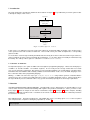
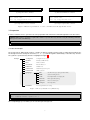
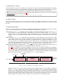
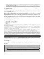
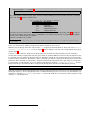
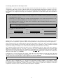
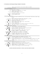
Institut f¨
ur Integrierte Systeme
Integrated Systems Laboratory
Department of Information Technology and Electrical Engineering
VLSI I: From Architectures to VLSI Circuits and FPGAs
227-0116-00L
Exercise 3
VHDL Synthesis
Prof. Dr. H. Kaeslin
Dr. N. Felber
SVN Rev.:
Last Changed:
1478
13-03-2015
Reminder:
With the execution of this training you declare that you understand and accept the regulations about using CAE/CAD
software installations at the ETH Zurich. These regulations can be read anytime at
http://eda.ee.ethz.ch/index.php/Regulations.
1 Introduction
The VLSI design flow is described in detail in the VLSI textbook. In Figure 1, a very rudimentary overview is given in order
to identify the subject of this exercise.
Specification
Algorithm Design
Architecture Design
VHDL Coding
behavioral VHDL
Synthesis
Netlist
Subject of this exercise
Physical Design
Chip Layout
Netlist
Figure 1: VLSI design flow overview.
In this exercise, you will learn to generate a gate-level netlist from a behavioral VHDL description of the circuit by means
of the synthesis tool S YNOPSYS D ESIGN C OMPILER. This tool will convert your VHDL description into a corresponding
gate-level netlist.
To ensure that a custom design can finally be fabricated at the foundry, the S YNOPSYS D ESIGN C OMPILER gets told to use
only a predefined selection of gates provided by the manufacturer, i.e., the gates which can actually be manufactured by
the foundry. The entirety of these gates are collected in a so-called standard cell library.
1.1 Software or Hardware
For all practical purposes, the syntax of VHDL is like most high-level programming languages. However the main purpose
of VHDL is to describe hardware. As hardware engineers, we are mostly forced to design circuits that meet certain
area, speed, and power requirements. We therefore need to know what hardware our carefully written code will result in.
Remember that each VHDL line will eventually contribute to the final hardware. In this sense, the VHDL language is more
like a schematic editor, than a programming language.
Writing good VHDL code is the first step to get exactly the desired circuit. Using realistic synthesis constraints with the
synthesis tools is the second step (you will learn how to set these constraints during this exercise). If done properly, these
two steps will allow you to describe and realize a very specific circuit that (hopefully) meets the design requirements.
2 Notation
Text-Based Command Inputs (Shell Commands): Throughout this exercise, different types of consoles will be used. In
order to avoid confusions and misunderstandings with regard to the provided commands (i.e., where you have to enter
them), Figure 2 shows an example of each of them. Furthermore, Figure 2c and Figure 2d illustrate examples, including
multiple-line commands and line breaks. It should be clear from the context in which window the commands provided in
the text have to be entered.
Files and Directories: File paths and directories, stated within this exercise, are always given relative to the root path of
your cockpit structure, except those during the preparation (cf. Section 3).
Student Task: Parts of the exercise where you are required to take action will be explained in a shaded box, just like
this paragraph.
2
cp /unspecified/shell.cmd .
sh >
(a) Unspecified shell command.
dvc >
dvc >
dvc >
cp /unix/shell.command .
(b) Standard UNIX shell command.
cp /this/is/a/design/vision/\
shell.cmd .
cp /copy/another.file .
dcs >
dcs >
dcs >
(c) Design Vision Console command.
cp /this/is/a/design/compiler/\
shell.cmd .
cp /copy/another.file .
(d) Design Compiler Shell command.
Figure 2: Different representations of console commands, used throughout this exercise.
3 Preparation
In order to start this exercise, you have to do some preparation work, which is described throughout the next subsections.
Student Task: Start by copying the required files and the respective directory structure using the following command
from your account’s root directory:
sh >
/home/vlsi1/u3/install.sh
3.1 Use the Cockpit
The design flow for digital circuits involves a number of different software packages that use different intermediate files.
The Design Center has developed an interface, i.e., a cockpit that will organize automatically a suited directory structure.
The synthesis-specific directory structure is highlighted in Figure 3.
design
.cockpitrc
Configuration for the cockpit
calibre
Final layout, DRC and LVS
docs
Links to documents
encounter
Place and Route tool
modelsim
Simulation tool
simvectors
Stimuli and expected responses
sourcecode
VHDL sourcecode
synopsys
tetramax
DDC
Save files for Synopsys (Synopsys native format)
WORK
Synthesis working directory
alib
Precompiled libraries for compile_ultra
netlist
Final output netlist (Verilog)
reports
Directory to write reports
scripts
Run scripts (TCL)
Test vector generation, test coverage
Figure 3: Directory structure for synthesis step.
Student Task: Change to the created directory and start the cockpit:
sh >
sh >
cd u3
icdesign umcL65 -update all &
The cockpit will pop up, from which you can start all required design tools.
3
4 Example I: GUI Guided Training
Basically, the S YNOPSYS D ESIGN C OMPILER tools can be subdivided into two major parts:
Design Vision: This is the graphical user interface (GUI) on top of the S YNOPSYS D ESIGN C OMPILER. It represents a
convenient way to interact with the compiler. Its main windows are illustrated in Figure 4 and explained in Section 4.1
and Section 4.2.
Design Compiler Shell (DC Shell): The DC Shell is a command-line-like tool, where all compiler commands can be typed
in as within a simple UNIX shell. The so called Tool Command Language (TCL) can be used in order to communicate
with the S YNOPSYS D ESIGN C OMPILER.
This part of the exercise represents a step-by-step example using the graphical user interface of the S YNOPSYS D ESIGN
C OMPILER. Thus, we will only make use of the Design Vision GUI, but we will come back to the DC Shell later in this
exercise.
4.1 Design Vision - Main Window
Now, let’s start the S YNOPSYS D ESIGN C OMPILER. In order to start the GUI of the S YNOPSYS D ESIGN C OMPILER choose
Design Vision-xg-t from the cockpit and click S YNOPSYS.
This will open a window of the Design Vision GUI. The main window (cf. Figure 4) hosts the Hierarchy Browser, Symbol,
and Schematic Viewer as well as the Console.
The menu bar with primary menus gives you access to commands, attributes, dialog boxes etc. In a second line you’ll find
shortcuts to commonly used commands.
Create Schematic
of Selected Objects
Online Help
& Man Pages
Hierarchy
Browser
Double click the hierarchy block
to open the schematic view.
Console
Window
Figure 4: Design Vision GUI interface to Design Compiler.
4
4.2 Design Vision - Console
The Design Vision Console provides a facility to enter commands in textual form, this way linking the graphical user-interface
to the command line interface (i.e., the DC Shell). Furthermore, all commands entered by mouse buttons are echoed here
in correct syntax. The command window also reflects all information displayed by reports and menu windows.
Note: Some specialized commands are not available through the graphical user interface. They must be entered in
the Design Vision Console or in the DC Shella .
a
To start the DC Shell in TCL mode use the cockpit with the DC Shell-xg-t option enabled.
4.3 Mouse Controls
The left mouse button is used to select one design object at a time. The middle mouse button is used to zoom. In the
display region use the right button to access the mouse menu. Among other things, the mouse menu is useful for zooming
the view.
4.4 Basic Synthesis Steps
Synthesis is a quite complex process, for which a more detailed explanation can be found in the VLSI textbook. Nevertheless, from a more abstract point of view, it can be subdivided into the following three main points:
Analyze Design: The analyze command converts the VHDL code into an intermediate format and stores it in a design
library (default: WORK ). Design libraries are the libraries you reference in VHDL using the library and use
statements. Once a design has been analyzed into a design library, it can be referenced from other (higher level)
designs. Special cases are VHDL packages, which have to be analyzed but not elaborated (they do not describe
designs).
Elaborate Design: The elaborate command reads a design unit from a design library into the S YNOPSYS D ESIGN C OM PILER memory. Referenced subdesigns are elaborated as well, if they can be found in the design library. For elaboration, VHDL generics can be set to their final values (overriding default values defined in the VHDL source code).
If you pass generics to an instantiated component in the VHDL code, the corresponding values will be propagated
to the subdesigns during elaboration. Generic values are appended to the base design name in S YNOPSYS D ESIGN
C OMPILER (an entity named adder will be named adder width8 if it has a generic width which is set to 8 ).
Compile Design: During the compilation process, the mapping of the generic logic and high level synthetic operators to
the available technology takes place. It can be initiated using the command compile_ultra.
Figure 5 shows optimization steps during compilation. In the first step, some high level mappings and optimizations
are done if the design is read in high-level (RTL) VHDL (or Verilog). The next step involves general boolean optimization. The logic can be flattened (converted to two-level logic) or structured (multi-level logic), for example. The last
step includes mapping to the target library and optimization, e.g. using complex gates available in the target library.
At the end, design rules (fanout, . . . ) are fixed and an area recovery step is performed.
Target Library
Generic Netlist
Constraints &
Attributes
Resource sharing
Implementation Selection
Operator Re-Ordering
Architectural Level
Flattening
Structuring
Logic Level
Combinational Mapping
Sequential Mapping
Design Rule Fixing
Optimized
Gate-Level
Netlist
Gate Level
Figure 5: Design optimization steps during compilation.
During the whole process, S YNOPSYS D ESIGN C OMPILER tries to attain the goals you set (you will learn setting these
goals, i.e., constraints, for the S YNOPSYS D ESIGN C OMPILER during this exercise). The constraints influence all the
steps involved. Setting timing constraints too tight will result in a large area. Per default, the S YNOPSYS D ESIGN
C OMPILER tries to fulfill the timing constraints first, then the area recovery step tries to reduce the area without
introducing new timing violations. Tight constraints will also lead to much longer compile times, since the S YNOPSYS
D ESIGN C OMPILER only stops when the constraints are met or when there is no more improvement.
5
Note: Although the command compile is still known by the S YNOPSYS D ESIGN C OMPILER, it has been replaced by compile_ultra. During this exercise, you may find the compile command somewhere, but this is
for demonstration purposes only.
4.5 The Sample Design
Now that you are familiar with the most important synthesis steps, we will explain how to use the S YNOPSYS D ESIGN
C OMPILER with the aid of a small sample design. Open the file ./sourcecode/crc4.vhd and have a look at the source. Make
sure you understand the design.
Start analyzing the design by selecting File→Analyze... in the Design Vision GUI. Press A DD... and in the pop-up
window select the file crc4.vhd. As library select WORK . You can tick the field Create new library if it doesn‘t exist. Click
OK to initiate the analyze step. You will not see any design in the Hierarchy Browser window as this command only checks
the syntax.
After having translated the VHDL source code, the next step in the S YNOPSYS D ESIGN C OMPILER synthesis flow is to build
a technology independent netlist, implementing the described behavior by means of generic circuit elements. Perform the
following steps in order to start the elaboration:
1. Navigate to File→Elaborate...
2. Select Library: WORK
3. Select Design: CRC4(BEHAVE CRC4)
4. Select Reanalyze out-of-date libraries
5. Click OK
You should now see an icon for crc4 in the Hierarchy Browser, indicating that the design is now present in S YNOPSYS
D ESIGN C OMPILER’s memory.
It is good practice to store your design after every important step in the synthesis flow. This eases potential re-iteration
steps. Select File→Save as... and change to the ./DDC directory in the Save Design dialog box that pops up. Save
the design in ∗.ddc format to a file named crc4.ddc.
Now, let us start mapping the circuit to the target library, i.e., perform the compilation step. Navigate to Design→\
Compile Design.... In the following pop-up window click the OK button to start the compilation of your design.
When the compilation finishes, the next step within the design flow is to make your design ready for further use in other
EDA tools. For that, you will now create a Verilog netlist from your design (which can later be read from other EDA tools).
In order to save your design as a Verilog netlist, you must first perform a simple conversion to adapt the internal S YNOPSYS
D ESIGN C OMPILER name definitions to standard Verilog definitions. Enter the following commands into the Design Vision
Console in order to perform the conversion:
dvc >
change_names -rule verilog -hierarchy
Afterwards, navigate to File→Save As..., select the netlists directory and enter the name crc4. Choose the format
VERILOG (v) and press S AVE. The netlist (crc4.v) is now ready for back-end design.
4.5.1 The Netlist
The Verilog netlist, which you have just created in the previous task, is a very widely accepted data format (i.e., can be read
by most of the CAE/CAD tools available on the market). Therefore, we will investigate it a little bit more in detail throughout
this section.
Student Task 1:
• All synthesis-related files can be found in the directory synopsys. Therefore, use a UNIX shell and change to
that directory first:
sh >
cd synopsys
• Next, navigate to the previously created netlist (If you have followed our instructions, it should be located in
./synopsys/netlists/).
6
• Open it using the less programa :
sh >
less crc4.v
The netlist contains a number of logic gates from the standard cell library, interconnected with some wires. Amongst
other cells, Table 1 lists those standard cells.
Table 1: Some gates of the standard cell library.
Standard Cell Description
ND2
DFQR
MUX2
XNR2
CKXOR2
2-Input NAND
D Flip-Flop
2-Bit Multiplexer
2-Input Exclusive Nor
2-Input Exclusive Or
Take paper and pencil and draw the schematic of the circuit by investigating the Verilog netlist (Table 1 may help you
in order to classify the gates of the netlist.). You do not need to draw the clock and the reset signal to every flip-flop,
because these signals are taken for granted.
Show the schematic to an assistant.
a
The less program only provides read-access to a file, and therefore guarantees that you do not make any unwanted changes to
the netlist.
The S YNOPSYS D ESIGN C OMPILER GUI is able to create schematics as well as symbols for a certain circuit on its own.
Hence, you can now check whether your previously drawn schematic is correct or not.
Switch back to the Design Vision GUI and select the crc4 design in the Hierarchy Browser. Next, click on the Create \
Schematic of Selected Objects icon (cf. Figure 4) and you will get a new view of the design with the three inputs
and the output1 .
In order to see the schematic, double click on the desgin in the schematic view. Does it match your own schematic?
You may have already recognized that each time you perform an operation within the S YNOPSYS D ESIGN C OMPILER GUI,
its command gets echoed in the Design Vision Console. During this example we only showed you how to use the GUI of the
S YNOPSYS D ESIGN C OMPILER. Nevertheless, all the commands can solely be entered in the Design Vision Console and
furthermore in the DC Shell as well. Because synthesis commands will repeat themselves quite often, it is good practice
to collect them in a script and later on you can start that script either by selecting File→Execute Script... (from the
Design Vision GUI) or by running the whole script (from the Design Vision Console or the DC Shell) by entering:
source ./scripts/synth.tcl
Currently, you have two different GUI windows of the S YNOPSYS D ESIGN C OMPILER opened. If you close the Design Vision
GUI by pressing the “x” at the top-right-hand corner, the DC Shell will stay opened. In order to close both windows, you
either have to navigate to File→Exit, or you enter exit into the DC Shell. Close the S YNOPSYS D ESIGN C OMPILER by
entering exit into the DC Shell.
1
Note that you can also observe the width of each I/O.
7
5 Example II: Getting to Grips with the Command Line
In the first exercise example you have learned what steps are necessary in order to synthesize a design described in VHDL
using the Design Vision GUI. Now we will treat the synthesis process more detailed by use of the DC Shell. This gives us
the opportunity to create command scripts, which can then be executed multiple times if required. Moreover, we will start
to deal with the definition of synthesis constraints.
5.1 Synthesis Constraints
Normally, a design has to respect a set of specifications (e.g., processing performance, area, power, etc.). The set of
specifications has to be given to the synthesis tool before the compilation process.
The constraints define your ”wishes” to the compiler. The compiler will do its best to map your HDL description into a netlist
that matches the constraints. Eventually, the compiler settles onto a circuit, the synthesized design. However, there is no
guarantee that the imposed constraints will be met. It is necessary, to check after the compilation if the circuit meets the
desired constraints. Sometimes the compiler will not be able to meet all the constraints. In this case you should do the
following:
• Check your constraints carefully, sometimes ”default” values found in example scripts may put unnecessary constraints on your design.
• If the circuit is only slightly larger/slower, a different compile optimization approach may help.
• If the performance gap is large (e.g., you needed a circuit working at 200 MHz, but the result is barely working with
100 MHz), you may have to step back and make architectural changes.
Throughout this and the next examples you will learn how to tell the S YNOPSYS D ESIGN C OMPILER to meet certain requirements.
5.2 The Sample Design
A gate-level schematic of the design you are dealing with during this example is illustrated in Figure 6. It represents a
hardware circuit of a generic Gray counter at the gate level. The necessary VHDL code is distributed over two design files,
namely:
graycnt.vhd
grayconv.vhd
The first file (graycnt.vhd) represents the circuit model to be synthesized and the second file is a package, made up of two
code conversion functions.
Before you proceed with the synthesis of these files, get acquired with them. Next, start the DC Shell by selecting DC
Shell-xg-t in the cockpit and press S YNOPSYS.
The window, which will pop up, represents the DC Shell. Compared to the Design Vision GUI (as described in the first
example in this exercise), the DC Shell does not provide a graphical user interface. Instead you can interact with the
S YNOPSYS D ESIGN C OMPILER based on textual commands. In order to get an idea on how powerful the DC Shell is, enter
the following command:
dcs >
help DC Shell Commands
This will show you a comprehensive list of the available commands within the DC Shell2 .
Note: If you are interested in detailed information about one of the commands, just enter man <command_name>.
This will show you the man pages of the respective command.
Now let us start building a synthesis script which may serve you as a base for further (more complex) scripts. Open the
file ./synopsys/scripts/synth.tcl and have a look at it. Throughout the whole script, you will find expressions bounded by
doubled angle brackets (e.g., <<Sample Expression>>). These expressions (including the bounding characters) will have
to be replaced by yourself during this example.
2
Don’t worry, you will only need a few of them in this exercise.
8
Student Task 2:
• In the following, the first two commands of the synthesis script are listeda .
remove_design -designs
sh rm -rf WORK/*
• Add a short description in the script and explain what these lines are doing b ?
• Enter the two commands into the DC Shell and execute them. Note that you can use the mouse in order to copy
the respective lines in the Tcl script by simply selecting them with the left mouse button and paste them into the
DC shell using the middle mouse button.
a
b
Comments in the script are initiated using the hash symbol.
The man pages may help you.
Create a command in order to analyze the two source files, which are part of the sample design and append it accordingly
in the synthesis script.
Note: If you cannot remember the exact syntax of the analyze command, one of the following hints may help you.
• Use the man pages (e.g. man analyze).
• Start the Design Vision GUI directly from the DC Shell by executing start_guia , do the analyze task there
and afterwards copy the command echoed in the Design Vision Console into your script.
a
Closing the Design Vision GUI can be achieved by entering stop_gui either in the Design Vision Console or in the DC Shell.
Proceed by determining a synthesis command for the elaborate step. In contrast to the previous example, this design
contains a generic parameter. Set that parameter to 5 from within your script. Again, refer to the previous note, if you do
not know the correct syntax of the elaborate command. Once again, execute the determined command.
If you now switch over to the Design Vision GUI again (If you have already closed it, you can start it again using the
start_gui command.), you will see the name of the design within the Hierarchy Browser, followed by the generic parameter values (e.g. graycnt GRAYWIDTH5 ).
As already mentioned earlier, every design is intended to fulfill some pre-defined requirements. One of the most important
constraints is the frequency with which the circuit is intended to run. Therefore, we will now set the target clock of our
sample design.
Insert the following lines of code into your synthesis script. Make sure that you insert it at the correct position (i.e., into the
Define Constraints section).
create_clock Clk_CI -period 1
This will set the target clock of the design to 1 GHz (i.e. a period of 1 ns).
Finally, you can compile your design using an appropriate command. Furthermore, insert that command in your synthesis script in order to use it again afterwards. This time, use the compile_ultra command in order to perform the
compilation.
As soon as you have found an appropriate compile command and inserted it into the synthesis script, the script should be
ready to re-run the whole synthesis flow without any further adaptions.
Re-run the whole synthesis flow using your script as follows:
dcs >
source ./scripts/synth.tcl
9
Afterwards you can check whether your re-run was successful or not with the check_design command.
Beside the S YNOPSYS D ESIGN C OMPILER commands you have inserted into the synthesis script on your own, some
already pre-defined commands exist. The section, displayed in the following, writes some reports about the synthesized
design into appropriate files:
# -------------------------------------------------------------------# Generate Reports
# -------------------------------------------------------------------report_timing > ./reports/timing.rpt
report_area -hierarchy > ./reports/area.rpt
report_register -nosplit > ./reports/registers.rpt
• The first command creates a report about timing information and stores it in the file ./reports/timing.rpt.
• The second command generates a report about the required area of the design. The output gets stored in the file
./reports/area.rpt and is represented using a hierarchical view. The values presented in the area report are given in
µm2 .
• The last row prints all registers within the design into the file ./reports/registers.rpt.
Note: The report commands, given in the synthesis script, represent only a small number of the available analysis
functionality of the S YNOPSYS D ESIGN C OMPILER. If you want to get a comprehensive list of the available report
commands within the S YNOPSYS D ESIGN C OMPILER, enter report into the DC Shell and then press TAB.
The second pre-defined section in the synthesis script creates the Verilog netlist as described in Example I in this exercise.
# -------------------------------------------------------------------# Write Out Data
# -------------------------------------------------------------------# Change names for Verilog.
change_names -rule verilog -hierarchy
# Write Verilog netlist.
write -hierarchy -format verilog -output ./netlists/graycnt.v
You may have recognized that for constrained timing paths, the command report_timing reports a value called slack.
If this value is positive, this means that the constraint set for the respective path has been met. If you get a value smaller
than zero, the respective path violates the timing constraint (i.e., has to be investigated further).
Student Task 3: Investigate the timing report a little bit more in detail and mark the critical path of the design within
the block diagram illustrated in Figure 6.
Does the design meet the timing requirements?
What is the value of the slack ?
Show your results of this example (the final synthesis script, the block diagram with the marked critical path, etc.) to
an assistant.
10
COUNT_DP_reg[4]
RST_RBI
CLK_CI
ENA_SI
Rst
E
D Q
COUNT_DO[4]
COUNT_DP_reg[3]
Rst
E
D Q
COUNT_DO[3]
COUNT_DP_reg[2]
Rst
E
D Q
COUNT_DO[2]
COUNT_DP_reg[1]
Rst
E
D Q
COUNT_DO[1]
COUNT_DP_reg[0]
Rst
E
D Q
Figure 6: Block diagram of the Gray Counter example.
11
COUNT_DO[0]
6 Example III: Constraining a Circuit
In this section, we will go through the synthesis process of a small design step by step and explore different constraints. Try
to understand all of the steps – for further explanations and more details please refer to the Synopsys Online Documentation
(SOLD), which can be launched using the following UNIX shell command:
sh >
synopsys-2014.09 sold
For the following steps we will use an example circuit that contains sequential cells as well as combinational parts. This
circuit could be part of the ALU inside the datapath of a processor, for doing some special kind of “multiply and accumulate”
operation. The sourcecode of the design can be found in the file ./sourcecode/datapath.vhd.
Have a look at the sourcecode in order to understand the design. If you did not yet start the cockpit, step into the root
directory of this exercise and start it:
sh >
sh >
cd u3
icdesign umcL65 &
Make sure that the DC Shell-xg-t option is selected and click S YNOPSYS in order to launch the DC Shell.
6.1 Initial Design
We will now guide you through the synthesis steps. You should already be familiar with many of the S YNOPSYS D ESIGN
C OMPILER commands mentioned throughout this example.
Note: Keep in mind what you have learned during the previous example of this exercise, i.e., that it might be a good
idea to build a script for all of your synthesis steps.
Analyze and elaborate the design:
dcs >
dcs >
analyze -format vhdl ../sourcecode/datapath.vhd
elaborate datapath
Now let’s just compile and see what will be generated by the S YNOPSYS D ESIGN C OMPILER.
dcs >
compile
Notice that the compilation process reports some information about the design. More detailed reports can be obtained by
means of S YNOPSYS D ESIGN C OMPILER’s report commands. As already mentioned during Example II, these commands
can be used to extract and analyze the performance figures of a synthesized netlist. Answer each of the following questions
by using the appropriate report command.
Student Task 4:
• What is the total cell area? A =
• What is the critical path length? tpd =
• What would be the maximum operating frequencya ? fmax =
• How many different references are used in this design? Nref =
• A single two-input ND2 gate occupies an area of 1 GE (Gate Equivalent). In the present technology (i.e., UMC
65 nm) the area required for a ND2 is equal to 1.44 µm2b . Determine the complexity of our current design in
gate equivalents. AreaGE =
a
b
Assume that registers are placed at the input and outputs with ideal timing parameters
For more information, check the corresponding entry in the DZ-Wiki under http://eda.ee.ethz.ch/index.php/UmcL65,
as well as the standard cell library application note and handbook available in your exercise directory under ./docs/\
stdcell low vt b03 appnote.pdf and ./docs/stdcell low vt b03 databook.pdf, respectively.
Note: Remember that most of your answers should have a measuring unit, otherwise they are meaningless.
12
6.2 Defining a Clock Period
In the above example, no constraints were given and the S YNOPSYS D ESIGN C OMPILER synthesized the design with the
minimum possible effort. The synthesis tool is able to extend its efforts to meet the specified timing constraints. Let us
have a look at what happens if we constrain the clock period of the circuit3 .
Remove the last design and start from scratch.
dcs >
dcs >
dcs >
remove_design -all
analyze -format vhdl ../sourcecode/datapath.vhd
elaborate datapath
The following command sets the clock period to 1 ns.
dcs >
create_clock Clk_CI -period 1.0
Now, we compile the circuit.
dcs >
compile
This time, the S YNOPSYS D ESIGN C OMPILER will try to come up with a netlist that meets the constrained clock period of
1 ns.
Student Task 5: Examine the resulting circuit by using the appropriate reporting commands. What is the effective
clock period and the required area now?
tpd =
A=
As one can see, the area is enlarged while the timing constraint is met. Furthermore, with the use of the command
report_reference, one can observe that the variety and specialization of the components has increased.
If you have investigated the timing reports of both the unconstrained and the constrained design in detail, you may have
recognized that the reported paths are different. Therefore, let us have a closer look at the different timings within a
sequential circuit.
6.3 Different Timing Paths
As depicted in Figure 7, the data paths of a sequential circuit can be subdivided into four categories with regard to their
timings:
combinational
circuitry
tio
i(k)
tso
present
input
tis
o(k)
present
output
tis : From input to state-holding registers (i → s),
tss
s(k)
present
state
state register
tss : From state-holding registers to state-holding registers (s → s),
s(k+1)
tso : From state-holding registers to output (s → o)
next
state
tio : From input to output (i → o).
CLK
Figure 7: Signal propagation paths through single-phase edge-triggered synchronous circuits.
3
Please refer to the VLSI 1 lecture notes for further information on timings.
13
Student Task 6: Using the report_timing command determine the timing information of the circuit. Which of the
timings illustrated in Figure 7 gets actually reported?
Which timing gets reported if you do not specify a clock constraint (i.e. the timing information gathered in Section 6.1)?
The four different timing paths of Figure 7 shall be investigated in the datapath.vhd circuit. Therefore, we need better
specified timing reports. In order to be able to report specific timing paths, we have to specify the start and/or end points
of the paths.
A meaningful starting point of a path is the input of our circuit (for tio and tis ) or the clock input of a flip-flop (for tso and tss ).
Similarly, the end points for a timing path are either circuit outputs (for tso and tio ) or the input pin of a flip-flop (for tis and
tss ).
Fortunately, it is easy to identify the inputs, outputs, and flip-flops within our netlist. This is because the S YNOPSYS D ESIGN
C OMPILER provides the commands all_registers, all_inputs and all_outputs. Furthermore, the command
report_cell can be used in order to report detailed information about logic cells. Registers will be named by the
S YNOPSYS D ESIGN C OMPILER by appending a “ reg” to the signal names. For example, a cell named DataxDP reg[14] is
certainly a flip-flop. Flip-flop clock pins are labeled with a CK .
Student Task 7: Use the commands all_registers, all_inputs, all_outputs, and report_cell to extract
specific cell information:
• Find all flip-flops and write down their names here:
• What is the name and the width of the data input?
Name =
Width =
• What is the name of the clock input?
Now, we have to combine the previously mentioned commands with the report_timing command in order to get all the
timing information illustrated in Figure 7 of our design. The start and the end points, which should be taken into consideration when using the report_timing command, can be determined using the arguments -from and -to, respectively. In
the following, an example printing the tis timing is given:
dcs >
report_timing -from [all_inputs] -to [all_registers -data_pins]
Student Task 8: By combining the report_timing command with the all_registers, all_inputs, and
all_outputs commands, complete the following timing information together with their respective slack:
tss =
tis =
tso =
tio =
slackss =
slackis =
slackso =
slackio =
What is the maximum clock frequency? Which one of the txy timing parameters dictates it?
fmax =
You are done with the first part of Exercise 3. Discuss your results with an assistant.
14
6.4 Input and Output Timing
In the following part we will examine the effect of the input and the output timing.
Input Timing: It is clear that the outputs of a circuit are not immediately available after the active clock edge. In our
example it takes roughly 0.74 ns for the outputs to appear after the active clock edge. This has to be taken into consideration
for the inputs of our circuit as well. More precisely, new inputs values will not be there immediately after the active clock
edge, a certain delay will elapse until our circuit sees valid data at its inputs.
Remove the design and start from scratch. Analyze, elaborate and constrain the design for a clock period of T = 1.0 ns,
then compile it. Continue with the constrained and compiled design, and add an input delay of 0.4 ns (Hint: man \
set_input_delay).
Output Timing: Try to imagine what happens when you sample the outputs of the design. The circuit doing the sampling
will see valid outputs only after a certain amount of time. Let us assume it will take 0.4 ns for all outputs to propagate
through the downstream circuit (i.e., the circuit connected to the outputs of our design). If this is the case, the data has to
be available at the output of our design already 0.4 ns in advance (that is: before the next active clock edge) such that the
downstream circuit is able to sample them correctly.
Student Task 9: Constrain the output timing in such a way that all outputs have settled 0.4 ns before the active
clock edge. This is to satisfy the downstream circuit that requires these 0.4 ns to sample our outputs correctly (Hint:
man set_output_delay). Check the reports now.
slackss =
slackis =
slackso =
slackio =
A=
As you can see, multiple timing violations occur in different paths. What has happened?
Up to now we have always looked at the most critical path in detail (every element on the path was visible). The following
command shows the worst 5 input to output paths with only their endpoints.
dcs >
report_timing -from [all_inputs] -to [all_outputs] -path end -max_paths 5
Student Task 10: Report the 10 worst register state to output paths (tso ) of the design. As you can see, there are
only a few paths violating the timing constraints. How many of them and what is the minimum/maximum slack of the
reported timing paths?
Nviolations =
slackmin =
slackmax =
Having seen that input and output timing add some additional constraints to the design, we have to include all the constraints
prior to compilation. The S YNOPSYS D ESIGN C OMPILER then considers these constraints and tries to meet the defined
requirements.
Student Task 11: Remove the design and start from scratch. Analyze, elaborate, set the input and output constraints
and then compile it. Now it is once more time to investigate all the different timing paths as well as the required area.
slackss =
slackis =
slackso =
slackio =
A=
Are there any open violating timing paths? If you check the reports now, what differences can you see? Can you
explain them?
15
6.5 Setting Input Drivers and Output Load
Input Drivers: In the next steps we want to investigate how the driver that drives the inputs of our circuit can affect the
overall timing. Until now the S YNOPSYS D ESIGN C OMPILER assumed ideal input signals that have infinitely steep edges.
In reality, our inputs are driven by the outputs of some other circuit with limited driving capabilities. That is, the edges of the
input signals to our design have finite ramp (rise and fall) times greater than zero and which depend on the input driver’s
strength.
Student Task 12:
• First, restart from scratch and compile the design, using the same constraints as before (A period of 1 ns, input
and output delays of 0.4 ns).
• Furthermore, let us add a driving cell constraint. Specify that all inputs of our circuit are being driven by a cell
that is equivalent in driving capability to the BUFM4W -cell (Hint: man set_driving_cell).
The following example describes the syntax of this command (To gather information about the library name,
have a look at the link command.):
dcs >
set_driving_cell -library <library_name> -lib_cell <cell_name> -pin \
<pin_name> [all_inputs]
• Investigate the timing information now.
slackss =
slackis =
slackso =
slackio =
A=
• What is the effect on the timing and on the area of the design (without compiling)?
Output Load: The propagation delay of a CMOS circuit depends also on the capacitive load it is driving at the outputs.
Basically, the more capacitance a gate has to drive, the longer it will take to charge (or discharge) the load capacitance.
At the moment we have not specified what is connected to the outputs of our circuit. Thus, the S YNOPSYS D ESIGN
C OMPILER assumes that there is no load connected to the outputs (i.e., the capacitance is equal to 0 F). But exactly that
may affect the timing considerably. Let us examine how much the output load can influence the timing.
Go on with the design from the previous task and use it as a starting point for this task. Have a look at the cell names
within one of the timing reports (e.g., ND2M2W , XOR2M2WA, etc.). The cell driving strength index is given by the digits
following the M character in the name of the standard cell. Depending on the cell, it ranges from 0 up to 48. For further
details, refer to the standard cell databook located in ./docs/stdcell low vt b03 databook.pdf. You will discover relatively low
drive gates at the outputs (e.g., ND2M2W).
Currently, there is no load connected to the outputs. Now, add a load corresponding to four times the load of the input
pin of the cell BUF1 to every output of the design (Hint: man set_load, man load_of). The following command is an
example and sets the load of all outputs equal to eight times the load of a BUFM4W:
dcs >
set_load [expr 8 * [load_of uk65lscllmvbbl_120c25_tc/BUFM4W/A]] [all_outputs]
Until now we have not modified the netlist, we have just changed the boundary conditions. It is possible to analyze
the timing under these conditions (without compiling a second time). If the S YNOPSYS D ESIGN C OMPILER knows about
the input driver and the output load ”in advance”, it is able (or at least it tries) to synthesize a netlist that can meet the
requirements. Therefore, these constraints should be added prior to compilation.
16
Student Task 13: Now, redo the compilation with the constraints listed in Table 2. Furthermore, keep the previously
determined input- and output-delays. For the last two columns of Table 2, you should have a look at the tSO timing
reports and write down the type of the gate at the respective output bit.
Table 2: Driving cell variations.
clock period
Specification
Driving Cell
Load
1.0 ns
1.0 ns
ideal
BUFM4W
ideal
8*BUFM4W
Cell Area [µm2 ]
Results
GateOut[0]
GateOut[7]
What conclusions can you derive from the results? What effect do the constraints on the driving cell and the load
have on the performance parameters?
6.6 Area/Timing Analysis
Student Task 14: Analyze the relationship between area and timing by constraining the present design with different
clock periods. Synthesize the design with the values listed in Table 3 and complete the missing numbers. For all of the
synthesis runs, set the input and output delays to 0.1 ns and do not use any input drivers and output loads. Moreover,
assure that you use a simple compile command in order to synthesize the design. For the empty Field (big: ) in the
first row of the table choose an appropriate value for the clock period.
Specification
Clock period T
Table 3: Clock period variations.
Results
Cell Area [GE] slackss [ns] T − slackss [ns]
big:
1.4 ns
1.2 ns
1.0 ns
0.8 ns
0.7 ns
0.6 ns
0.4 ns
0.0 ns
Use the following figure to plot your results as an AT graphic and show them to an assistant.
1400
1300
Area [GE]
1200
1100
1000
900
800
700
600
0.4
0.6
0.8
1
Clock Period - Slack [ns]
17
1.2
Be aware of the fact that the compilation steps will take longer and longer. The compiler has to push all its efforts to the
limit for increasing constraints!
7 Example IV: Magnitude Comparator
Our final example is located in the source file ./sourcecode/comparator.vhd and is a purely combinational 4-bit magnitude
comparator.
Student Task 15:
• Have a look at the VHDL code. Two binary inputs are compared to each other. If the first number is equal,
smaller, or larger than the second number, separate outputs are set accordingly.
• Now, synthesize the code and investigate the log, reports and resulting netlist. Note that while elaborating
the VHDL file, you have to set the parameter WIDTH : set it to 4 (Hint: elaborate <design_name> \
-parameters "<parameters> = XX").
• Are there some additional cells, which you had not intended?
• Correct the source code such as to prevent those cells from being inferred. After having changed the source
code, you have to perform an RTL simulation to verify the correct functionality of it. For that, we have already
prepared a testbench, which is located at ./sourcecode/comparator tb.vhd. For the simulation, you can use the
script located at ./modelsim/comparator compile rtl.csh
• Show your source code correction and the simulation results to an assistant.
18
8 Synthesis Hints
Throughout this section, some useful hints with regard to synthesis will be given. They may help you during this exercise
or during one of your future VLSI projects.
8.1 DesignVision
Command echoing The command echoing feature in the GUI is useful to become familiar with the S YNOPSYS D ESIGN
C OMPILER command syntax. Use the history command in order to see a list of all previously executed commands.
A script file can be generated by history -h > scripts/scriptfile.tcl. This file may then be edited and
run by means of the command source or the menu option File→Execute Script....
Graphical interface Most of the S YNOPSYS D ESIGN C OMPILER commands are available via the menu driven graphical
interface. However, some of the more versatile commands and specific command options have to be entered in
textual form. Use the help command to see a list of available commands.
Command option Most command options can be abbreviated to their shortest equivalent form (e.g., -h for -hierarchy,
. . . ). There have been some cases, where the full option worked but the abbreviated form did not work, however.
Commands response A successfully executed command is signaled by a 1 at the end of the associated report. A 0
indicates that the command failed. Be aware that certain commands (like analyzing a design file with more than
one design unit) involve multiple actions each of which is attributed a 1 or 0. Always apply yourself to the reports
generated and note any warnings issued by S YNOPSYS D ESIGN C OMPILER.
8.2 DC Shell
Startup The more you will use S YNOPSYS D ESIGN C OMPILER, the less you will use the GUI version of it. Starting the DC
Shell always from the cockpit may become annoying, because you have to start the cockpit first. Instead, you can
run the DC Shell from a UNIX shell using the command synopsys dc_shell-xg-t.
Manpages If you are looking for a certain command argument, but cannot remember the exact syntax, just have a look at
the manpage of the respective command (e.g., man create_clock). This definitely works out faster than browsing
through hundreds of pages within the S YNOPSYS D ESIGN C OMPILER manual, looking for the respective command.
8.3 Warnings
Warning and error messages: Synopsys can be very talkative. Sometimes you get buried in information, warning, and
error messages. Nevertheless, you should try to understand all these messages and not just ignore them. Often they
contain valuable hints and information, pointing to possible design problems or flaws.
Old data: Beware of old data lying around and causing problems. This might be data in the S YNOPSYS D ESIGN C OMPILER
memory, in design libraries or .ddc files on your search path. If you think your changes aren’t included or get
inexplicable problems, try cleaning all old data: remove all designs from memory, remove all files in your design
libraries and remove any unneeded .ddc file, especially in your working directory. It might be a good idea to save .ddc
files to a directory that is not on the S YNOPSYS D ESIGN C OMPILER’s search path, except for the ones you specifically
want to be included (use list search_path to check your path).
8.4 Design Objects
Cells & instances: S YNOPSYS D ESIGN C OMPILER does not make use of the terms cell and instance in a consistent way.
In general, they can be conceived to be synonyms in the context of S YNOPSYS D ESIGN C OMPILER.
Locate: To locate specific design objects in the schematic view use the menu entry Select→By Name.... In the command mode you can identify specific design objects by means of the find and filter commands.
Find: For finding all design objects of a particular type, shorthand commands exists (e.g., all_inputs, all_outputs,
all_registers).
19
9 Commonly used Synopsys Design Compiler Commands
Table 4: A short cheatsheet for the Synopsys Design Compiler.
Command Description
User Interface Commands
help List available commands
man Displays reference manual pages of a command
history Lists previously entered commands
sh Execute shell commands
source Read a file and evaluate it as a Tcl script
gui start Starts the application GUI
gui stop Stops the application GUI
exit
Design Database Commands
analyze Reads and analyzes the HDL files and stores the intermediate format in the specified design
library
elaborate Builds a design from the intermediate format (maps to gtech lib)
remove design Removes the designs or libraries from memory
check design Checks the current design for consistency
find Finds a design or library object
list instances Lists the instances in the current design or current instance
write Writes a design netlist to a file
current design Sets the working design
link Resolves design references (shows libraries and if there are black boxes)
write script Writes shell commands to save the current settings
Attribute and Constraint Commands
set attribute Sets an attribute to an object (cell, clock...)
create clock Creates a clock object and defines its waveform
set max delay Specifies a maximum delay target for paths in the current design
set driving cell Define the cell drives of the specified ports
set drive Define the driver’s strength to a driver of the specified ports
set load Sets the load attribute of the specified ports
load of Returns the capacitance of the specified library cell pin
set input delay Sets input delay on ports relative to a clock signal
set output delay Sets output delay on ports relative to a clock signal
all inputs Returns the input and inout ports of the current design
all outputs Returns the output and inout ports of the current design
all registers Returns the sequential cells of the current design
Optimization Commands
compile Performs the synthesis and optimization on the current design
compile ultra Performs a high-effort compile on the current design
set ungroup Sets the attribute that blocks are to be ungrouped during compile
set flatten Sets/unset the flatten attribute to enable or disable the flattening optimization step during
compile
set map only Sets the attribute so that they are excluded from logiclevel optimization during compile
Report and Analysis Commands
report timing Displays timing information about a design
report area Displays area information for the current design or instance
report hierarchy Displays the reference hierarchy of the current instance or design
report design Displays attributes of the current design
report net fanout Displays net fanout or buffer tree information for the current design
check timing Checks for possible timing problems in the current design
You have reached the end of Exercise 3. Discuss your results with an assistant.
20