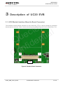
1
UC20 EVB User Guide
UMTS/HSPA Series
Rev. UC20_EVB_User_Guide_V1.0
Date: 2013-06-04
www.quectel.com
UMTS/HSPA
UC20 EVB User Guide
Our aim is to provide customers with timely and comprehensive service. For any
assistance, please contact our company headquarter:
Quectel Wireless Solutions Co., Ltd.
Room 501, Building 13, No.99, Tianzhou Road, Shanghai, China, 200233
Tel: +86 21 5108 6236
Mail: [email protected]
l
e
t
l
c
a
e
i
t
u
n
Q ide
f
n
o
C
Or our local office, for more information, please visit:
http://www.quectel.com/support/salesupport.aspx
For technical support, to report documentation errors, please visit:
http://www.quectel.com/support/techsupport.aspx
GENERAL NOTES
QUECTEL OFFERS THIS INFORMATION AS A SERVICE TO ITS CUSTOMERS. THE INFORMATION
PROVIDED IS BASED UPON CUSTOMERS’ REQUIREMENTS. QUECTEL MAKES EVERY EFFORT
TO ENSURE THE QUALITY OF THE INFORMATION IT MAKES AVAILABLE. QUECTEL DOES NOT
MAKE ANY WARRANTY AS TO THE INFORMATION CONTAINED HEREIN, AND DOES NOT ACCEPT
ANY LIABILITY FOR ANY INJURY, LOSS OR DAMAGE OF ANY KIND INCURRED BY USE OF OR
RELIANCE UPON THE INFORMATION. THE INFORMATION SUPPLIED HEREIN IS SUBJECT TO
CHANGE WITHOUT PRIOR NOTICE.
COPYRIGHT
THIS INFORMATION CONTAINED HERE IS PROPRIETARY TECHNICAL INFORMATION OF
QUECTEL CO., LTD. TRANSMITTABLE, REPRODUCTION, DISSEMINATION AND EDITING OF THIS
DOCUMENT AS WELL AS UTILIZATION OF THIS CONTENTS ARE FORBIDDEN WITHOUT
PERMISSION. OFFENDERS WILL BE HELD LIABLE FOR PAYMENT OF DAMAGES. ALL RIGHTS
ARE RESERVED IN THE EVENT OF A PATENT GRANT OR REGISTRATION OF A UTILITY MODEL
OR DESIGN.
Copyright © Quectel Wireless Solutions Co., Ltd. 2013. All rights reserved.
UC20_EVB_User_Guide
Confidential / Released
1 / 25
UMTS/HSPA
UC20 EVB User Guide
About the document
History
Revision
1.0
l
e
t
l
c
a
e
i
t
u
n
Q ide
f
n
o
C
Date
Author
Description
2013-05-31
Jerry You
Initial
UC20_EVB_User_Guide
Confidential / Released
2 / 25
UMTS/HSPA
UC20 EVB User Guide
Contents
About the document ................................................................................................................................... 2
Contents ....................................................................................................................................................... 3
Table Index ................................................................................................................................................... 4
Figure Index ................................................................................................................................................. 5
1
Introduction .......................................................................................................................................... 6
1.1. Safety Information ........................................................................................................................ 7
2
General Overview ................................................................................................................................. 9
2.1. Key Features ................................................................................................................................ 9
2.2. System Overview ....................................................................................................................... 10
2.3. UC20 TE-A and UC20 EVB_V1.01 ............................................................................................ 11
3
Description of UC20 EVB .................................................................................................................. 13
3.1. UC20 Module Interface (Board to Board Connector) ................................................................ 13
3.2. Test Points of UC20 ................................................................................................................... 16
3.3. SIM Card Interface ..................................................................................................................... 17
3.4. USB Device Interface ................................................................................................................. 18
3.5. RS-232 Interface ........................................................................................................................ 19
3.6. Switch and Buttons .................................................................................................................... 21
3.7. Status LEDs ............................................................................................................................... 22
3.8. Analog Audio Interface ............................................................................................................... 22
4
Operating Procedure for UC20 ......................................................................................................... 24
4.1. Turn on UC20 Module ................................................................................................................ 24
4.2. Turn off UC20 Module ................................................................................................................ 24
4.3. Reset .......................................................................................................................................... 25
4.4. Communication via USB or Serial Port ...................................................................................... 25
l
e
t
l
c
a
e
i
t
u
n
Q ide
f
n
o
C
UC20_EVB_User_Guide
Confidential / Released
3 / 25
UMTS/HSPA
UC20 EVB User Guide
Table Index
TABLE 1: FEATURES .......................................................................................................................................... 9
TABLE 2: PIN ASSIGNMENT OF B2B CONNECTOR ...................................................................................... 14
TABLE 3: PIN ASSIGNMENT ............................................................................................................................ 16
TABLE 4: PIN ASSIGNMENT-SIM CARD HOLDER J502 ................................................................................ 18
TABLE 5: PIN ASSIGNMENT-MAIN UART ....................................................................................................... 20
TABLE 6: FUNCTION OF SWITCH AND BUTTONS ........................................................................................ 21
l
e
t
l
c
a
e
i
t
u
n
Q ide
f
n
o
C
TABLE 7: DESCRIPTION OF LEDS ................................................................................................................. 22
TABLE 8: STATE OF NET_STATUS.................................................................................................................. 24
UC20_EVB_User_Guide
Confidential / Released
4 / 25
UMTS/HSPA
UC20 EVB User Guide
Figure Index
FIGURE 1: SYSTEM OVERVIEW ..................................................................................................................... 10
FIGURE 2: FIGURE OF UC20 TE-A AND UC20 EVB_V1.01 ............................................................................ 11
FIGURE 3: FIGURE OF ACCESSORIES.......................................................................................................... 12
FIGURE 4: BOARD TO BOARD CONNECTOR ............................................................................................... 13
FIGURE 5: TEST POINTS................................................................................................................................. 16
FIGURE 6: SIM1 INTERFACE .......................................................................................................................... 17
l
e
t
l
c
a
e
i
t
u
n
Q ide
f
n
o
C
FIGURE 7: MOLEX SIM CARD HOLDER ......................................................................................................... 17
FIGURE 8: USB INTERFACE ........................................................................................................................... 18
FIGURE 9: UART BLOCK DIAGRAM ............................................................................................................... 19
FIGURE 10: LEVEL MATCH CIRCUIT .............................................................................................................. 19
FIGURE 11: MAIN UART PORT ........................................................................................................................ 20
FIGURE 12: SWITCH AND BUTTONS ............................................................................................................. 21
FIGURE 13: LEDS ............................................................................................................................................. 22
FIGURE 14: AUDIO CODEC CIRCUIT ............................................................................................................. 23
UC20_EVB_User_Guide
Confidential / Released
5 / 25
UMTS/HSPA
UC20 EVB User Guide
1
Introduction
This document describes UC20 Evaluation Board Rev.1.01. The UC20 Evaluation Board is designed to
assist system integrator in developing and evaluating products based on Quectel Wireless Modules.
l
e
t
l
c
a
e
i
t
u
n
Q ide
f
n
o
C
This document gives a detailed description for interfaces of the UC20 module, provides technical
specifications and presents guidelines on how to connect UC20 module with UC20 Evaluation Board
Rev.1.01 and operate UC20 module.
UC20_EVB_User_Guide
Confidential / Released
6 / 25
UMTS/HSPA
UC20 EVB User Guide
1.1. Safety Information
The following safety precautions must be observed during all phases of the operation, such as usage,
service or repair of any cellular terminal or mobile incorporating module. Manufacturers of the cellular
terminal should send the following safety information to users and operating personnel and to incorporate
these guidelines into all manuals supplied with the product. If not so, Quectel does not take on any liability
for customer failure to comply with these precautions.
l
e
t
l
c
a
e
i
t
u
n
Q ide
f
n
o
C
Full attention must be given to driving at all times in order to reduce the risk of an
accident. Using a mobie while driving (even with a handsfree kit) cause distraction
and can lead to an accident. You must comply with laws and regulations restricting
the use of wireless devices while driving.
Switch off the cellular terminal or mobile before boarding an aircraft. Make sure it
switched off. The operation of wireless appliances in an aircraft is forbidden to
prevent interference with communication systems. Consult the airline staff about
the use of wireless devices on boarding the aircraft, if your device offers a Fight
Mode which must be enabled prior to boarding an aircraft.
Switch off your wireless device when in hospitals or clinics or other health care
facilities. These requests are desinged to prevent possible interference with
sentitive medical equipment.
GSM cellular terminals or mobiles operate over radio frequency signal and cellular
network and cannot be guaranteed to connect in all conditions, for example no
mobile fee or an invalid SIM card. While you are in this condition and need
emergent help, please remember using emergency call. In order to make or
receive call, the cellular terminal or mobile must be switched on and in a service
area with adequate cellular signal strength.
Your cellular terminal or mobile contains a transmitter and receiver. When it is ON ,
it receives and transmits radio frequency energy. RF interference can occur if it is
used close to TV set, radio, computer or other electric equipment.
UC20_EVB_User_Guide
Confidential / Released
7 / 25
UMTS/HSPA
UC20 EVB User Guide
In locations with potencially explosive atmospheres, obey all posted signs to turn
off wireless devices such as your phone or other cellular terminals. Areas with
potencially exposive atmospheres including fuelling areas, below decks on boats,
fuel or chemical transfer or storage facilities, areas where the air contains
chemicals or particles such as grain, dust or metal powders.
l
e
t
l
c
a
e
i
t
u
n
Q ide
f
n
o
C
UC20_EVB_User_Guide
Confidential / Released
8 / 25
UMTS/HSPA
UC20 EVB User Guide
2
General Overview
l
e
t
l
c
a
e
i
t
u
n
Q ide
f
n
o
C
2.1. Key Features
Table 1: Features
Feature
Implementation
Power supply
DC supply 4.5~5.5V
VBAT: 3.4V~4.3V at J102
SIM Interface
SIM1 Card (8 pins) connector with front tray loading and support card
detection
SIM2 Card (6 pins) connector with bottom tray loading and does not
support card detection ( reserved)
Support SIM cards: 3V and 1.8V
Audio Interface
One analog interface for connecting a handset or headset
Serial Interface
Two RS-232 interfaces:
COM1-serial interface for data communication (default 115200bps)
COM2-serial interface for debug purpose (reserved)
Max. baud rate: 460800 bps
USB Interface
High speed
Signal Indication
4 LEDS are available for signal indication
Physical Characteristics
Size: 13.6*10.6 cm
UC20_EVB_User_Guide
Confidential / Released
9 / 25
UMTS/HSPA
UC20 EVB User Guide
2.2. System Overview
COM1
l
e
t
l
c
a
e
i
t
u
n
Q ide
f
n
o
C
Debug
Port
Main
Port
UC20
B2B
COM2
LEDS
PCM
CODEC
SIM Card
DC
Power
Power
Switch
USB
PWRKEY
Button
RESET
Button
Analog
Audio
Figure 1: System Overview
UC20_EVB_User_Guide
Confidential / Released
10 / 25
UMTS/HSPA
UC20 EVB User Guide
2.3. UC20 TE-A and UC20 EVB_V1.01
3G
GPS
Antenna Antenna
Diversity
Reception
l
e
t
l
c
a
e
i
t
u
n
Q ide
f
n
o
C
Figure 2: UC20 TE-A and UC20 EVB_V1.01
UC20_EVB_User_Guide
Confidential / Released
11 / 25
UMTS/HSPA
UC20 EVB User Guide
RS232
Cable
GPS
Antenna
l
e
t
l
c
a
e
i
t
u
n
Q ide
f
n
o
C
DC 5V
Adaptor
USB
Cable
MAIN
Antenna
RF Cable
Headset
Figure 3: Accessories
UC20_EVB_User_Guide
Confidential / Released
12 / 25
UMTS/HSPA
UC20 EVB User Guide
3
Description of UC20 EVB
l
e
t
l
c
a
e
i
t
u
n
Q ide
f
n
o
C
3.1. UC20 Module Interface (Board to Board Connector)
The Panasonic board-to-board connector on the UC20 EVB_1.01 is a 100-pin double-row receptacle.
Several pins are reserved. Table 2 shows the names and positions of the pins on the UC20 EVB_V1.01.
100
2
99
1
J101
Figure 4: Board to Board Connector
UC20_EVB_User_Guide
Confidential / Released
13 / 25
UMTS/HSPA
UC20 EVB User Guide
Table 2: PIN Assignment of B2B Connector
Pin No.
Signal Name
Pin No.
Signal Name
1
GND
2
GND
3
GND
4
SIM_GND
5
RESERVED
6
SIM_RST
RESERVED
8
SIM_CLK
RESERVED
10
SIM_DATA
RESERVED
12
SIM_VDD
RESERVED
14
SIM_PRESENCE
RESERVED
16
GND
RESERVED
18
RESERVED
RESERVED
20
RESERVED
RESERVED
22
RESERVED
AGND
24
RESERVED
PCM_IN
26
RESERVED
PCM_OUT
28
RESERVED
PCM_SYNC
30
RESERVED
PCM_CLK
32
RESERVED
GND
34
RESERVED
35
I2C_SDA
36
RESERVED
37
I2C_SCL
38
GND
39
GND
40
DEBUG_TXD
41
RESERVED
42
DEBUG_RXD
43
RESET_N
44
RESERVED
45
PWRKEY
46
RESERVED
7
9
11
13
15
17
19
21
23
25
27
29
31
33
l
e
t
l
c
a
e
i
t
u
n
Q ide
f
n
o
C
UC20_EVB_User_Guide
Confidential / Released
14 / 25
UMTS/HSPA
UC20 EVB User Guide
47
GND
48
RESERVED
49
ADC1
50
RESERVED
51
GND
52
RESERVED
53
ADC0
54
GND
55
GND
56
RESERVED
57
l
e
t
l
c
a
e
i
t
u
n
Q ide
f
n
o
C
RESERVED
58
RESERVED
VRTC
60
RESERVED
STATUS
62
RESERVED
RESERVED
64
GND
NET_STATUS
66
VDD_EXT
NET_MODE
68
RI
RESERVED
70
DCD
RESERVED
72
CTS
RESERVED
74
RTS
GND
76
DTR
USB_DP
78
TXD
USB_DM
80
RXD
GND
82
RESERVED
USB_VBUS
84
RESERVED
RESERVED
86
RESERVED
87
RESERVED
88
RESERVED
89
RESERVED
90
RESERVED
91
GND
92
GND
93
GND
94
GND
95
VBAT
96
GND
97
VBAT
98
VBAT
59
61
63
65
67
69
71
73
75
77
79
81
83
85
UC20_EVB_User_Guide
Confidential / Released
15 / 25
UMTS/HSPA
UC20 EVB User Guide
99
VBAT
100
VBAT
NOTE
These pins connect directly with UC20 pins.
l
e
t
l
c
a
e
i
t
u
n
Q ide
f
n
o
C
3.2. Test Points of UC20
Header J701 are the test pins at the UC20 EVB_V1.01. Figure 5 shows the test points.
Figure 5: Test Points
Table 3: PIN Assignment
Pin No.
30
28
26
24
22
Signal Name
TXD
CTS
DTR
RXD
RTS
20
DCD
18
RI
16
GND
NOTES
1. These test pins belong to 3.3V power domain which is converted from UC20 Main UART pins.
UC20_EVB_User_Guide
Confidential / Released
16 / 25
UMTS/HSPA
UC20 EVB User Guide
2. The other pins are reserved.
3.3. SIM Card Interface
The UC20 EVB_V1.01 has two integrated SIM card interfaces. But SIM2 is reserved. A suitable SIM card
(3V or 1.8V) is required to start UC20 module. The SIM card holder J502 placed on the UC20
_EVB_V1.01 is from type Molex. Figure 5 shows the simplified interface schematic.
l
e
t
l
c
a
e
i
t
u
n
Q ide
f
n
o
C
SIM Card Holder
B2B Connector
J502
4
4
1
2
3
12
6
8
6
10
J101
Figure 6: SIM1 Interface
Figure 7: Molex SIM Card Holder
UC20_EVB_User_Guide
Confidential / Released
17 / 25
UMTS/HSPA
UC20 EVB User Guide
Table 4: Pin Assignment-SIM Card Holder J502
Pin No.
Signal Name
I/O
Function
1
SIM_VDD
O
Supply voltage U=3V or 1.8V for SIM1
card, generated by the module.
2
SIM_RST
O
SIM1 card reset..
3
SIM_CLK
O
SIM1 card clock.
4,8
5
6
7
l
e
t
l
c
a
e
i
t
u
n
Q ide
f
n
o
C
GND
/
Ground
VPP
/
Not connected.
SIM_DATA
I/O
Data line, bi-directional
SIM_PRESENCE
I
SIM1 card detection.
3.4. USB Device Interface
UC20 EVB_V1.01 provides a USB 2.0 High Speed interface. It is used for AT command, data transfer and
firmware upgrading.
J601
USB
Figure 8: USB Interface
UC20_EVB_User_Guide
Confidential / Released
18 / 25
UMTS/HSPA
UC20 EVB User Guide
3.5. RS-232 Interface
UC20 EVB_V1.01 offers two RS-232 interfaces: COM1 (MAIN UART) and COM2. COM2 is reserved.
The serial interface COM1 of the UC20 EVB_V1.01 is intended for the communication between UC20
module and the host application. The interface is a data and control interface for transmitting data and AT
command.
l
e
t
l
c
a
e
i
t
u
n
Q ide
f
n
o
C
Module
DB9
Connector
Level Shifter
UART Port
Figure 9: UART Block Diagram
Figure 10 shows the reference design of RS-233 level shifter.
SP3238
28
25
3.3V
1.8V
VCCA
DCD
TXD
CTS
RI
DCD_1.8V
TXD_1.8V
CTS_1.8V
RI_1.8V
RXD
DTR
RTS
GND
RXD_1.8V
DTR_1.8V
RTS_1.8V
GND
3
VCCB
24
23
22
19
DCD
DCD_3.3V
TXD
TXD_3.3V
CTS
CTS_3.3V
RI_3.3V
RI
Voltage
Level
MODULE
Translator
Module
1
GND
17
16
21
20
18
RXD_3.3V
RXD
DTR
DTR_3.3V
RTS
RTS_3.3V
3V
3.3V
13
C 1+
V+
C 1-
GND
C 2+
VCC
C 2-
V-
T1IN
T2IN
T3IN
T4IN
T5IN
/R1OUT
R1OUT
R2OUT
R3OUT
T4OUT
T2OUT
T3OUT
T1OUT
T5OUT
R1IN
R2IN
R3IN
27
2
26
4
GND
3V
3.3V
GND
10
6
7
5
12
8
9
11
ONLINE
15
/STATUS
14
/ SHUTDOWN
6
7
8
9
TO PC serial port
1
2
3
4
5
GND
Figure 10: Level Match Circuit
UC20_EVB_User_Guide
Confidential / Released
19 / 25
UMTS/HSPA
UC20 EVB User Guide
6
7
8
9
1
2
3
4
5
l
e
t
l
c
a
e
i
t
u
n
Q ide
f
n
o
C
Figure 11: Main UART Port
Table 5: Pin Assignment-Main UART
Pin No.
1
2
3
4
5
6
7
8
9
Signal Name
I/O
Description
DCD
O
Data carrier detection
RXD
I
Receive data
TXD
O
Transmit data
DTR
I
Data terminal ready
GND
/
GND
NC
/
NC
RTS
I
Request to send
CTS
O
Clear to send
RI
O
Ring indicator
NOTE
These pins are RS232 voltage level.
UC20_EVB_User_Guide
Confidential / Released
20 / 25
UMTS/HSPA
UC20 EVB User Guide
3.6. Switch and Buttons
UC20 EVB_V1.01 comprises two buttons and one switch. Figure 12 shows the switch and buttons.
l
e
t
l
c
a
e
i
t
u
n
Q ide
f
n
o
C
S201
S202
S203
Figure 12: Switch and Buttons
Table 6: Functionality of switch and buttons
Reference
S201
S202
S203
UC20_EVB_User_Guide
Functionality
Power supply
Turn on/off UC20 module
Restart UC20 module
Confidential / Released
21 / 25
UMTS/HSPA
UC20 EVB User Guide
3.7. Status LEDs
UC20 EVB_V1.01 comprises several status LEDs. Figure 13 shows the position of LEDs.
D102
D104
D101
D103
l
e
t
l
c
a
e
i
t
u
n
Q ide
f
n
o
C
Figure 13: LEDs
Table 7: Description of LEDs
Reference
D103
D101
D104
D102
Description
PWR_LED, power supply is ready.
STATUS, indicates UC20 module is in ON or OFF status.
NET_MODE, module works in 2G networks or 3G networks.
NET_STATUS, indicate UC20 module’s working status.
3.8. Analog Audio Interface
UC20 Module just provides digital audio interface (PCM). UC20 EVB_V1.01 equips an external audio
codec called NAU8814, which transfer PCM to analogy signal. There is one analogy audio interface at
UC20 EVB_V1.01. Analogy signal could be input and output via RJ11 or audio jack. Figure 14 shows
audio codec circuit.
UC20_EVB_User_Guide
Confidential / Released
22 / 25
MCLK
BCLK
UC20 PCM_CLK
PCM_SYNC
PCM_OUT
PCM_IN
FS
MIC_BIAS
MIC+
MIC-
MIC_BIAS
UMTS/HSPA
UC20 EVB User Guide
DACIN
CODEC
ADCOUT
NAU8814
SPKOUT+
I2C_SCL
SCLK
SDIN
l
e
t
l
c
a
e
i
t
u
n
Q ide
f
n
o
C
10K
10K
I2C_SDA
SPKOUT-
UC20 EVB_1.01
1.8V
Figure 14: Audio Codec Circuit
UC20_EVB_User_Guide
Confidential / Released
23 / 25
UMTS/HSPA
UC20 EVB User Guide
4
Operating Procedure for UC20
4.1. Turn on UC20 Module
l
e
t
l
c
a
e
i
t
u
n
Q ide
f
n
o
C
1. Connecting the UC20-TE-A module to the connector on UC20 EVB_V1.01, charging the 5V power
adapter, pulling up S201 to ON state, D103 (PWR_LED) will be bright.
2. Pressing the S202 (PWRKEY) for at least 100ms then release. The D101 (STATUS) will be light and
indicates power-on mode.
3. The D102 (NET_STATUS) will be blinking at a certain frequency. The network status of the module
can be judged by this LED. The working state of the Net Light is shown as below:
Table 8: State of NET_STATUS
State
Description
0.2s On/ 1.8s Off
The module is not synchronized with network.
1.8s On/ 0.2s Off
Idle mode.
0.125s On/ 0.125s Off
Data transfer is ongoing via GSM/3G network.
always on
Calling
NOTE
DC 5V adaptor is recommended for power supply and USB cable could be used as power supply as well
(max current is 500 mA).
4.2. Turn off UC20 Module
There are several ways to turn off UC20 module.
One way to switch off the module is using the AT command AT+QPWD=1. It is best and safest approach.
This procedure lets the module log off from the network and save data before it is shut down. The other
way to switch off the module is pressing S202 (PWRKEY) at least 0.5 second and release, the module will
be shut down after then.
UC20_EVB_User_Guide
Confidential / Released
24 / 25
UMTS/HSPA
UC20 EVB User Guide
4.3. Reset
The emergency restart option is only used in the case of emergency. In this situation, due to serious
problem, the software is not responding for more than 5 seconds.
Pulling down the module’s RESET_N pin by pressing the key S203 (more than 100ms) causes at release
a reset of UC20 Module. This may cause the loss of information stored in the memory since the reset is
initialized.
l
e
t
l
c
a
e
i
t
u
n
Q ide
f
n
o
C
4.4. Communication via USB or Serial Port
1.
2.
Install USB drive at PC or Laptop.
Power on UC20 module, select communication port number as
.
3.
4.
Configure AT Command Window, correct baud rate and port.
Operate the module via AT commands.
UC20_EVB_User_Guide
Confidential / Released
25 / 25