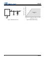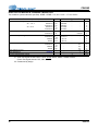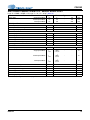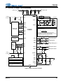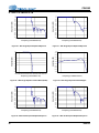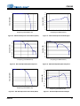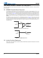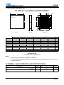
1
CS4265 104 dB, 24-Bit, 192 kHz Stereo Audio CODEC D/A Features A/D Features Multi-Bit Delta Sigma Modulator Multi-Bit Delta Sigma Modulator 104 dB Dynamic Range 104 dB Dynamic Range -90 dB THD+N -95 dB THD+N Up to 192 kHz Sampling Rates Stereo 2:1 Input Multiplexer Single-Ended Analog Architecture Programmable Gain Amplifier (PGA) – – Volume Control with Soft Ramp – – 0.5 dB Step Size Zero Crossing, Click-Free Transitions Pseudo-Differential Stereo Line Inputs ® Stereo Microphone Inputs Popguard Technology – Minimizes the Effects of Output Transients Filtered Line-Level Outputs Selectable Serial Audio Interface Formats – – – Left-Justified up to 24-bit I²S up to 24-bit Right-Justified 16-, 18-, 20-, and 24-bit Selectable 50/15 µs De-Emphasis 1.8 V to 5 V Reset PCM Serial Interface / Loopback Register Configuration I2C Control Data – – +32 dB Gain Stage Low-Noise Bias Supply Up to 192 kHz Sampling Rates Selectable Serial Audio Interface Formats – Left-Justified up to 24-bit – I²S up to 24-bit High-Pass Filter or DC Offset Calibration 3.3 V to 5 V Level Translator Serial Audio Output Level Translator Serial Audio Input ± 12 dB Gain, 0.5 dB Step Size Zero Crossing, Click-Free Transitions Volume Control Interpolation Filter Multibit Modulator Switched Capacitor DAC and Filter Volume Control Interpolation Filter Multibit Modulator Switched Capacitor DAC and Filter Left DAC Output Mute Control Transmitter Output Internal Voltage Reference High Pass Filter Mute Control Right DAC Output IEC60958-3 Transmitter High Pass Filter http://www.cirrus.com 3.3 V to 5 V Low-Latency Anti-Alias Filter Multibit Oversampling ADC Low-Latency Anti-Alias Filter Multibit Oversampling ADC Copyright Cirrus Logic, Inc. 2012 (All Rights Reserved) Microphone Bias Mic Bias +32 dB PGA MUX PGA +32 dB Mic Input 1&2 Stereo Line Input AUG '12 DS657F3 CS4265 System Features Synchronous IEC60958-3 Transmitter – Up to 192 kHz Sampling Rates – 75 Drive Capability Serial Audio Data Input Multiplexer Internal Digital Loopback Supports Master or Slave Operation Mute Output Control Power-Down Mode – Available for A/D, D/A, CODEC, Mic Preamplifier +3.3 V to +5 V Analog Power Supply +3.3 V to +5 V Digital Power Supply Direct Interface with 1.8 V to 5 V Logic Levels Supports I²C® Control Port Interface General Description The CS4265 is a highly integrated stereo audio CODEC. The CS4265 performs stereo analog-to-digital (A/D) and digital-to-analog (D/A) conversion of up to 24-bit serial values at sample rates up to 192 kHz. A 2:1 stereo input multiplexer is included for s electing between line-level or microphone-level inputs. The microphone input path includes a +32 dB gain stage and a low noise bias voltage supply. The PGA is availa ble for line or microphone inputs and provides gain or attenuation of 12 dB in 0.5 dB steps. The output of the PGA is followed by an advanced 5thorder, multi-bit delta sigma modulator and digital filtering/decimation. Sampled data is transmitted by the serial audio interface at rates from 4 kHz to 192 kHz in either Slave or Master Mode. The D/A converter is based on a 4th-order multi-bit delta sigma modulator with an ultra-linear low-pass filter and offers a volume control that operates with a 0.5 dB step size. It in corporates selectable soft ramp and zero crossing transition functions to eliminate clicks and pops. Standard 50/15 s de-emphasis is availa ble for a 44.1 kHz sample rate for compatibility with digital audio programs mastered using the 50 /15 s pre-emphasis technique. Integrated level translators allow ea sy interfacing between the CS4265 and other devices operating over a wide range of logic levels. The CS4265 is available in a 32-pin QFN package for both Commercial (-10° to +70° C) and Automotive (-40° to +105° C) grade. The CDB4265 is also available for device evaluation and implementation suggestions. Please refer to “Ordering Information” on page 57 for complete details. 2 DS657F3 CS4265 TABLE OF CONTENTS 1. PIN DESCRIPTIONS .......................................................................................................................... 7 2. CHARACTERISTICS AND SPECIFICATIONS ...................................................................................... 9 SPECIFIED OPERATING CONDITIONS ............................................................................................. 9 ABSOLUTE MAXIMUM RATINGS ....................................................................................................... 9 DAC ANALOG CHARACTERISTICS ................................................................................................. 10 DAC COMBINED INTERPOLATION & ON-CHIP ANALOG FILTER RESPONSE ............................ 11 ADC ANALOG CHARACTERISTICS ................................................................................................. 13 ADC ANALOG CHARACTERISTICS ................................................................................................. 15 ADC DIGITAL FILTER CHARACTERISTICS ..................................................................................... 16 DC ELECTRICAL CHARACTERISTICS ............................................................................................. 17 DIGITAL INTERFACE CHARACTERISTICS ...................................................................................... 18 SWITCHING CHARACTERISTICS - SERIAL AUDIO PORT ............................................................. 19 SWITCHING CHARACTERISTICS - I²C CONTROL PORT ............................................................... 22 3. TYPICAL CONNECTION DIAGRAM ................................................................................................... 23 4. APPLICATIONS ................................................................................................................................... 24 4.1 Recommended Power-Up Sequence ............................................................................................. 24 4.2 System Clocking ............................................................................................................................. 24 4.2.1 Master Clock ......................................................................................................................... 24 4.2.2 Master Mode ......................................................................................................................... 25 4.2.3 Slave Mode ........................................................................................................................... 25 4.3 High-Pass Filter and DC Offset Calibration .................................................................................... 25 4.4 Analog Input Multiplexer, PGA, and Mic Gain ................................................................................ 27 4.5 Input Connections ........................................................................................................................... 27 4.5.1 Pseudo-Differential Input ....................................................................................................... 27 4.6 Output Connections ........................................................................................................................ 28 4.7 Output Transient Control ................................................................................................................ 28 4.7.1 Power-Up .............................................................................................................................. 28 4.7.2 Power-Down .......................................................................................................................... 28 4.7.3 Serial Interface Clock Changes ............................................................................................. 28 4.8 DAC Serial Data Input Multiplexer .................................................................................................. 29 4.9 De-Emphasis Filter ......................................................................................................................... 29 4.10 Internal Digital Loopback .............................................................................................................. 29 4.11 Mute Control ................................................................................................................................. 30 4.12 AES3 Transmitter ......................................................................................................................... 30 4.12.1 TxOut Driver ........................................................................................................................ 30 4.12.2 Mono Mode Operation ......................................................................................................... 31 4.13 I²C Control Port Description and Timing ....................................................................................... 31 4.14 Status Reporting ........................................................................................................................... 32 4.15 Reset ............................................................................................................................................ 33 4.16 Synchronization of Multiple Devices ............................................................................................. 33 4.17 Grounding and Power Supply Decoupling .................................................................................... 33 4.18 Package Considerations ............................................................................................................... 33 5. REGISTER QUICK REFERENCE ........................................................................................................ 34 6. REGISTER DESCRIPTION .................................................................................................................. 36 6.1 Chip ID - Register 01h .................................................................................................................... 36 6.2 Power Control - Address 02h ......................................................................................................... 36 6.2.1 Freeze (Bit 7) ......................................................................................................................... 36 6.2.2 Power-Down MIC (Bit 3) ........................................................................................................ 36 6.2.3 Power-Down ADC (Bit 2) ....................................................................................................... 36 6.2.4 Power-Down DAC (Bit 1) ....................................................................................................... 37 6.2.5 Power-Down Device (Bit 0) ................................................................................................... 37 6.3 DAC Control - Address 03h ............................................................................................................ 37 DS657F3 3 CS4265 6.3.1 DAC Digital Interface Format (Bits 5:4) ................................................................................. 37 6.3.2 Mute DAC (Bit 2) ................................................................................................................... 37 6.3.3 De-Emphasis Control (Bit 1) .................................................................................................. 38 6.4 ADC Control - Address 04h ............................................................................................................ 38 6.4.1 Functional Mode (Bits 7:6) .................................................................................................... 38 6.4.2 ADC Digital Interface Format (Bit 4) ...................................................................................... 38 6.4.3 Mute ADC (Bit 2) ................................................................................................................... 39 6.4.4 ADC High-Pass Filter Freeze (Bit 1) ..................................................................................... 39 6.4.5 Master / Slave Mode (Bit 0) ................................................................................................... 39 6.5 MCLK Frequency - Address 05h .................................................................................................... 39 6.5.1 Master Clock Dividers (Bits 6:4) ............................................................................................ 39 6.6 Signal Selection - Address 06h ...................................................................................................... 40 6.6.1 DAC SDIN Source (Bit 7) ...................................................................................................... 40 6.6.2 Digital Loopback (Bit 1) ......................................................................................................... 40 6.7 Channel B PGA Control - Address 07h .......................................................................................... 40 6.7.1 Channel B PGA Gain (Bits 5:0) ............................................................................................. 40 6.8 Channel A PGA Control - Address 08h .......................................................................................... 40 6.8.1 Channel A PGA Gain (Bits 5:0) ............................................................................................. 40 6.9 ADC Input Control - Address 09h ................................................................................................... 41 6.9.1 PGA Soft Ramp or Zero Cross Enable (Bits 4:3) .................................................................. 41 6.9.2 Analog Input Selection (Bit 0) ................................................................................................ 41 6.10 DAC Channel A Volume Control - Address 0Ah ........................................................................... 41 6.11 DAC Channel B Volume Control - Address 0Bh ........................................................................... 42 6.11.1 Volume Control (Bits 7:0) .................................................................................................... 42 6.12 DAC Control 2 - Address 0Ch ...................................................................................................... 42 6.12.1 DAC Soft Ramp or Zero Cross Enable (Bits 7:6) ................................................................ 42 6.12.2 Invert DAC Output (Bit 5) .................................................................................................... 43 6.13 Status - Address 0Dh ................................................................................................................... 43 6.13.1 E to F C-Buffer Transfer ...................................................................................................... 43 6.13.2 Clock Error (Bit 3) ................................................................................................................ 43 6.13.3 ADC Overflow (Bit 1) ........................................................................................................... 43 6.13.4 ADC Underflow (Bit 0) ......................................................................................................... 43 6.14 Status Mask - Address 0Eh .......................................................................................................... 44 6.15 Status Mode MSB - Address 0Fh ................................................................................................. 44 6.16 Status Mode LSB - Address 10h .................................................................................................. 44 6.17 Transmitter Control 1 - Address 11h ............................................................................................ 44 6.17.1 E to F C-Data Buffer Transfer Inhibit (Bit 6) ........................................................................ 44 6.17.2 C-Data Access Mode (Bit 5) ................................................................................................ 44 6.18 Transmitter Control 2 - Address 12h ............................................................................................ 45 6.18.1 Transmitter Digital Interface Format (Bits 7:6) .................................................................... 45 6.18.2 Transmitter Output Driver Control (Bit 5) ............................................................................. 45 6.18.3 Transmitter Mute Control (Bit 4) .......................................................................................... 45 6.18.4 Transmitted Validity Bit Control (Bit 3) ................................................................................ 45 6.18.5 Transmitter Mono/Stereo Operation Control (Bit 2) ............................................................. 45 6.18.6 Mono Mode CS Data Source (Bit 1) .................................................................................... 45 6.18.7 Mono Mode Channel Selection (Bit 0) ................................................................................. 46 7. PARAMETER DEFINITIONS ................................................................................................................ 47 8. DAC FILTER PLOTS .................................................................................................................... 48 9. ADC FILTER PLOTS ......................................................................................................................... 50 10. EXTERNAL IEC60958-3 TRANSMITTER COMPONENTS ............................................................... 52 10.1 IEC60958-3 Transmitter External Components ............................................................................ 52 10.2 Isolating Transformer Requirements ............................................................................................ 52 11. CHANNEL STATUS BUFFER MANAGEMENT ................................................................................ 53 11.1 IEC60958-3 Channel Status (C) Bit Management ........................................................................ 53 4 DS657F3 CS4265 11.1.1 Accessing the E Buffer ........................................................................................................ 54 11.2 Serial Copy Management System (SCMS) .................................................................................. 54 11.3 Channel Status Data E Buffer Access .......................................................................................... 54 11.3.1 One-Byte Mode ................................................................................................................... 55 11.3.2 Two-Byte Mode ................................................................................................................... 55 12. PACKAGE DIMENSIONS .................................................................................................................. 56 13. THERMAL CHARACTERISTICS AND SPECIFICATIONS ............................................................... 56 14. ORDERING INFORMATION ........................................................................................................ 57 15. REVISION HISTORY .......................................................................................................................... 57 LIST OF FIGURES Figure 1.DAC Output Test Load ................................................................................................................ 12 Figure 2.Maximum DAC Loading .............................................................................................................. 12 Figure 3.Master Mode Serial Audio Port Timing ....................................................................................... 20 Figure 4.Slave Mode Serial Audio Port Timing ......................................................................................... 20 Figure 5.Format 0, Left-Justified up to 24-Bit Data ................................................................................... 21 Figure 6.Format 1, I²S up to 24-Bit Data ................................................................................................... 21 Figure 7.Format 2, Right-Justified 16-Bit Data. Format 3, Right-Justified 24-Bit Data. ....................................................................................................... 21 Figure 8.Control Port Timing - I²C Format ................................................................................................. 22 Figure 9.Typical Connection Diagram ....................................................................................................... 23 Figure 10.Master Mode Clocking .............................................................................................................. 25 Figure 11.Analog Input Architecture .......................................................................................................... 27 Figure 12.Pseudo-Differential Input Stage ................................................................................................ 28 Figure 13.De-Emphasis Curve .................................................................................................................. 29 Figure 14.Suggested Active-Low Mute Circuit .......................................................................................... 30 Figure 15.Control Port Timing, I²C Write ................................................................................................... 32 Figure 16.Control Port Timing, I²C Read ................................................................................................... 32 Figure 17.De-Emphasis Curve .................................................................................................................. 38 Figure 18.DAC Single-Speed Stopband Rejection ................................................................................... 48 Figure 19.DAC Single-Speed Transition Band .......................................................................................... 48 Figure 20.DAC Single-Speed Transition Band .......................................................................................... 48 Figure 21.DAC Single-Speed Passband Ripple ........................................................................................ 48 Figure 22.DAC Double-Speed Stopband Rejection .................................................................................. 48 Figure 23.DAC Double-Speed Transition Band ........................................................................................ 48 Figure 24.DAC Double-Speed Transition Band ........................................................................................ 49 Figure 25.DAC Double-Speed Passband Ripple ...................................................................................... 49 Figure 26.DAC Quad-Speed Stopband Rejection ..................................................................................... 49 Figure 27.DAC Quad-Speed Transition Band ........................................................................................... 49 Figure 28.DAC Quad-Speed Transition Band ........................................................................................... 49 Figure 29.DAC Quad-Speed Passband Ripple ......................................................................................... 49 Figure 30.ADC Single-Speed Stopband Rejection ................................................................................... 50 Figure 31.ADC Single-Speed Stopband Rejection ................................................................................... 50 Figure 32.ADC Single-Speed Transition Band (Detail) ............................................................................. 50 Figure 33.ADC Single-Speed Passband Ripple ........................................................................................ 50 Figure 34.ADC Double-Speed Stopband Rejection .................................................................................. 50 Figure 35.ADC Double-Speed Stopband Rejection .................................................................................. 50 Figure 36.ADC Double-Speed Transition Band (Detail) ............................................................................ 51 Figure 37.ADC Double-Speed Passband Ripple ...................................................................................... 51 Figure 38.ADC Quad-Speed Stopband Rejection ..................................................................................... 51 Figure 39.ADC Quad-Speed Stopband Rejection ..................................................................................... 51 Figure 40.ADC Quad-Speed Transition Band (Detail) .............................................................................. 51 Figure 41.ADC Quad-Speed Passband Ripple ......................................................................................... 51 DS657F3 5 CS4265 Figure 42.Consumer Output Circuit (VD = 5 V) ........................................................................................ 52 Figure 43.TTL/CMOS Output Circuit ......................................................................................................... 52 Figure 44.Channel Status Data Buffer Structure ....................................................................................... 53 Figure 45.Flowchart for Writing the E Buffer ............................................................................................. 54 LIST OF TABLES Table 1. Speed Modes .............................................................................................................................. 24 Table 2. Common Clock Frequencies ....................................................................................................... 24 Table 3. MCLK Dividers ............................................................................................................................ 25 Table 4. Slave Mode Serial Bit Clock Ratios ............................................................................................. 25 Table 5. Device Revision .......................................................................................................................... 36 Table 6. Freeze-able Bits .......................................................................................................................... 36 Table 7. DAC Digital Interface Formats .................................................................................................... 37 Table 8. De-Emphasis Control .................................................................................................................. 38 Table 9. Functional Mode Selection .......................................................................................................... 38 Table 10. ADC Digital Interface Formats .................................................................................................. 39 Table 11. MCLK Frequency ...................................................................................................................... 39 Table 12. DAC SDIN Source Selection ..................................................................................................... 40 Table 13. Example Gain and Attenuation Settings ................................................................................... 40 Table 14. PGA Soft Cross or Zero Cross Mode Selection ........................................................................ 41 Table 15. Analog Input Selection .............................................................................................................. 41 Table 16. Digital Volume Control Example Settings ................................................................................. 42 Table 17. DAC Soft Cross or Zero Cross Mode Selection ........................................................................ 43 Table 18. Transmitter Digital Interface Formats ........................................................................................ 45 6 DS657F3 CS4265 TXOUT VD DGND MCLK LRCK SCLK SDOUT SDIN1 1. PIN DESCRIPTIONS 32 31 30 29 28 27 26 25 SDA 1 24 SDIN2 SCL 2 23 TXSDIN VLC 3 22 VLS RESET 4 21 MUTEC VA 5 20 AOUTB AGND 6 19 AOUTA AINA 7 18 AGND AINB 8 17 VA Thermal Pad 9 10 11 12 13 14 15 16 SGND AFILTA AFILTB VQ FILT+ MICIN1 MICIN2 MICBIAS Top-Down (Through Package) View 32-Pin QFN Package Pin Name # Pin Description SDA 1 Serial Control Data (Input/Output) - Bidirectional data line for the I²C control port. SCL 2 Serial Control Port Clock (Input) - Serial clock for the I²C control port. 3 Control Port Power (Input) - Determines the required signal level for the control port interface. Refer to the Recommended Operating Conditions for appropriate voltages. RESET 4 Reset (Input) - The device enters a low-power mode when this pin is driven low. VA 5 Analog Power (Input) - Positive power for the internal analog section. AGND 6 Analog Ground (Input) - Ground reference for the internal analog section. AINA AINB 7, 8 Analog Input (Input) - The full-scale level is specified in the ADC Analog Characteristics specification table. SGND 9 Signal Ground (Input) - Ground reference for the analog line inputs. AFILTA AFILTB 10, 11 Antialias Filter Connection (Output) - Antialias filter connection for the ADC inputs. VQ 12 Quiescent Voltage (Output) - Filter connection for internal quiescent voltage. FILT+ 13 Positive Voltage Reference (Output) - Positive reference voltage for the internal sampling circuits. MICIN1 MICIN2 14, 15 Microphone Input (Input) - The full-scale level is specified in the ADC Analog Characteristics specification table. 16 Microphone Bias (Output) - Low noise bias supply for external microphone. Electrical characteristics are specified in the DC Electrical Characteristics table. VLC MICBIAS DS657F3 7 CS4265 VA 17 Analog Power (Input) - Positive power for the internal analog section. AGND 18 Analog Ground (Input) - Ground reference for the internal analog section. AOUTA AOUTB MUTEC VLS TXSDIN 19, 20 Analog Audio Output (Output) - The full scale output level is specified in the DAC Analog Characteristics specification table. 21 Mute Control (Output) - This pin is active during power-up initialization, reset, muting, when master clock left/right clock frequency ratio is incorrect, or power-down. 22 Serial Audio Interface Power (Input) - Determines the required signal level for the serial audio interface. Refer to the Recommended Operating Conditions for appropriate voltages. 23 Transmitter Serial Audio Data Input (Input) - Input for two’s complement serial audio data. SDIN2 24 Serial Audio Data Input 2 (Input) - Input for two’s complement serial audio data. SDIN1 25 Serial Audio Data Input 1 (Input) - Input for two’s complement serial audio data. SDOUT 26 Serial Audio Data Output (Output) - Output for two’s complement serial audio data. SCLK 27 Serial Clock (Input/Output) - Serial clock for the serial audio interface. 28 Left Right Clock (Input/Output) - Determines which channel, Left or Right, is currently active on the serial audio data line. MCLK 29 Master Clock (Input) - Clock source for the delta-sigma modulators. DGND 30 Digital Ground (Input) - Ground reference for the internal digital section. VD 31 Digital Power (Input) - Positive power for the internal digital section. TXOUT 32 Transmitter Line Driver Output (Output) - IEC60958-3 driver output. LRCK Thermal Pad 8 - Thermal Pad - Thermal relief pad for optimized heat dissipation. DS657F3 CS4265 2. CHARACTERISTICS AND SPECIFICATIONS SPECIFIED OPERATING CONDITIONS AGND = DGND = 0 V; All voltages with respect to ground. Parameters DC Power Supplies: Symbol Min Nom Max Units VA VD VLS VLC TA 3.13 3.13 1.71 1.71 -10 5.0 3.3 3.3 3.3 - 5.25 (Note 1) 5.25 5.25 +70 V V V V C Analog Digital Logic - Serial Port Logic - Control Port Ambient Operating Temperature (Power Applied) Notes: 1. Maximum of VA+0.25 V or 5.25 V, whichever is less. ABSOLUTE MAXIMUM RATINGS AGND = DGND = 0 V All voltages with respect to ground. (Note 2) Parameter Symbol Min Max Units VA VD VLS VLC Iin -0.3 -0.3 -0.3 -0.3 +6.0 +6.0 +6.0 +6.0 V V V V - 10 mA VINA AGND-0.3 VA+0.3 V VIND-S VIND-C -0.3 -0.3 VLS+0.3 VLC+0.3 V V Ambient Operating Temperature (Power Applied) TA -50 +125 C Storage Temperature Tstg -65 +150 C DC Power Supplies: Input Current Analog Digital Logic - Serial Port Logic - Control Port (Note 3) Analog Input Voltage Digital Input Voltage Logic - Serial Port Logic - Control Port 2. Operation beyond these limits may result in permanent damage to the device. Normal operation is not guaranteed at these extremes. 3. Any pin except supplies. Transient currents of up to ±100 mA on the analog input pins will not cause SCR latch-up. DS657F3 9 CS4265 DAC ANALOG CHARACTERISTICS Test Conditions (unless otherwise specified): AGND = DGND = 0 V; VA = 3.13 V to 5.25 V; VD = 3.13 V to 5.25 V or VA + 0.25 V, whichever is less; VLS = VLC = 1.71 V to 5.25 V; TA = -10° to +70° C for Commercial or -40° to +85° C for Automotive; Output test signal: 997 Hz full-scale sine wave; Test load RL = 3 k, CL = 10 pF (see Figure 1), Fs = 48/96/192 kHz. Measurement Bandwidth 10 Hz to 20 kHz; All Connections as shown in Figure 9 on page 23. Commercial Grade Parameter Symbol Automotive Grade Min Typ Max Min Typ Max Unit 98 95 90 87 104 101 96 93 - 96 93 88 85 104 101 96 93 - dB dB dB dB - -90 -81 -41 -93 -73 -33 -84 -87 - - -90 -81 -41 -93 -73 -33 -82 -85 - dB dB dB dB dB dB 95 92 88 85 101 98 93 90 - 93 90 86 83 101 98 93 90 - dB dB dB dB - -87 -78 -38 -90 -70 -30 -79 -82 - - -87 -78 -38 -90 -70 -30 -77 -80 - dB dB dB dB dB dB - 100 - - 100 - dB Interchannel Gain Mismatch - 0.1 0.25 - 0.1 0.25 dB Gain Drift - 100 - - 100 - ppm/°C Dynamic Performance for VA = 4.75 V to 5.25 V Dynamic Range 18 to 24-Bit 16-Bit (Note 4) A-Weighted unweighted A-Weighted unweighted Total Harmonic Distortion + Noise 18 to 24-Bit (Note 4) 0 dB -20 dB -60 dB THD+N 0 dB -20 dB -60 dB 16-Bit Dynamic Performance for VA = 3.13 V to 3.46 V Dynamic Range 18 to 24-Bit 16-Bit (Note 4) A-Weighted unweighted A-Weighted unweighted Total Harmonic Distortion + Noise 18 to 24-Bit 16-Bit Interchannel Isolation (Note 4) 0 dB -20 dB -60 dB THD+N 0 dB -20 dB -60 dB (1 kHz) DC Accuracy Analog Output Full Scale Output Voltage 0.60*VA 0.65*VA 0.70*VA 0.60*VA 0.65*VA 0.70*VA Vpp DC Current draw from an AOUT pin (Note 5) IOUT - - 10 - - 10 A AC-Load Resistance (Note 6) RL 3 - - 3 - - k Load Capacitance (Note 6) CL - - 100 - - 100 pF ZOUT - 150 - - 150 - Output Impedance 4. One-half LSB of triangular PDF dither added to data. 5. Guaranteed by design. The DC current draw represents the allowed current draw from the AOUT pin due to typical leakage through the electrolytic DC blocking capacitors. 10 DS657F3 CS4265 6. Guaranteed by design. See Figure 2. RL and CL reflect the recommended minimum resistance and maximum capacitance required for the internal op-amp’s stability. CL affects the dominant pole of the internal output amp; increasing CL beyond 100 pF can cause the internal op-amp to become unstable. DAC COMBINED INTERPOLATION & ON-CHIP ANALOG FILTER RESPONSE Parameter (Note 7,10) Symbol Combined Digital and On-chip Analog Filter Response Passband (Note 7) Min Typ Max Unit Single-Speed Mode to -0.1 dB corner to -3 dB corner 0 0 - 0.35 0.4992 Fs Fs Frequency Response 10 Hz to 20 kHz -0.175 - +0.01 dB StopBand 0.5465 - - Fs 50 - - dB - 10/Fs - s - - +0.05/-0.25 dB StopBand Attenuation (Note 8) Group Delay De-emphasis Error (Note 9) tgd Fs = 44.1 kHz Combined Digital and On-chip Analog Filter Response Passband (Note 7) Double-Speed Mode to -0.1 dB corner to -3 dB corner Frequency Response 10 Hz to 20 kHz StopBand StopBand Attenuation (Note 8) Group Delay tgd 0 0 - 0.22 0.501 Fs Fs -0.15 - +0.15 dB 0.5770 - - Fs 55 - - dB - 5/Fs - s Combined Digital and On-chip Analog Filter Response Quad-Speed Mode Passband (Note 7) 0 0 - 0.110 0.469 Fs Fs -0.12 - 0 dB 0.7 - - Fs 51 - - dB - 2.5/Fs - s to -0.1 dB corner to -3 dB corner Frequency Response 10 Hz to 20 kHz StopBand StopBand Attenuation (Note 8) Group Delay tgd 7. Filter response is guaranteed by design. 8. For Single-Speed Mode, the Measurement Bandwidth is 0.5465 Fs to 3 Fs. For Double-Speed Mode, the Measurement Bandwidth is 0.577 Fs to 1.4 Fs. For Quad-Speed Mode, the Measurement Bandwidth is 0.7 Fs to 1 Fs. 9. De-emphasis is available only in Single-Speed Mode. 10. Response is clock dependent and will scale with Fs. Note that the amplitude vs. frequency plots of this data (Figures 18 to 27) have been normalized to Fs and can be de-normalized by multiplying the X-axis scale by Fs. DS657F3 11 CS4265 3.3 µF V out AOUTx R L AGND C L Capacitive Load -- C L (pF) 125 100 75 25 2.5 3 Figure 1. DAC Output Test Load 12 Safe Operating Region 50 5 10 15 20 Resistive Load -- RL (k ) Figure 2. Maximum DAC Loading DS657F3 CS4265 ADC ANALOG CHARACTERISTICS Test conditions (unless otherwise specified): AGND = DGND = 0 V; VA = 3.13 V to 5.25 V; VD = 3.13 V to 5.25 V or VA + 0.25 V, whichever is less; VLS = VLC = 1.71 V to 5.25 V; TA = -10° to +70° C for Commercial or -40° to +85° C for Automotive; Input test signal: 1 kHz sine wave; measurement bandwidth is 10 Hz to 20 kHz; Fs = 48/96/192 kHz.; All connections as shown in Figure 9 on page 23. Line-Level Inputs Parameter Dynamic Performance for VA = 4.75 V to 5.25 V Dynamic Range (Note 13) (Note 13) Symbol PGA Setting: -12 dB to +6 dB A-weighted unweighted 40 kHz bandwidth unweighted PGA Setting: +12 dB Gain A-weighted unweighted 40 kHz bandwidth unweighted Typ Max Unit 98 95 - 104 101 98 - dB dB dB 92 89 - 98 95 92 - dB dB dB - -95 -81 -41 -92 -89 - dB dB dB dB - -92 -75 -35 -89 -86 - dB dB dB dB 93 90 - 101 98 95 - dB dB dB 89 86 - 95 92 89 - dB dB dB - -92 -78 -38 -84 -86 - dB dB dB dB - -89 -72 -32 -81 -83 - dB dB dB dB Total Harmonic Distortion + Noise (Note 13) (Note 13) (Note 12) PGA Setting: -12 dB to +6 dB -1 dB -20 dB -60 dB 40 kHz bandwidth -1 dB PGA Setting: +12 dB Gain -1 dB -20 dB -60 dB 40 kHz bandwidth -1 dB Min THD+N Dynamic Performance for VA = 3.13 V to 3.46 V Dynamic Range (Note 13) (Note 13) PGA Setting: -12 dB to +6 dB A-weighted unweighted 40 kHz bandwidth unweighted PGA Setting: +12 dB Gain A-weighted unweighted 40 kHz bandwidth unweighted Total Harmonic Distortion + Noise (Note 13) (Note 13) (Note 12) PGA Setting: -12 dB to +6 dB -1 dB -20 dB -60 dB 40 kHz bandwidth -1 dB PGA Setting: +12 dB Gain -1 dB -20 dB -60 dB 40 kHz bandwidth -1 dB THD+N Line-Level Inputs Commercial Grade Parameter Interchannel Isolation DS657F3 Symbol Min Typ Max Unit - 90 - dB 13 CS4265 DC Accuracy Gain Error Gain Drift - 100 10 - % ppm/°C 0.51*VA 6.12 0.57*VA 6.8 0.63*VA 7.48 Vpp k - 5 - % Line-Level Input Characteristics Full-scale Input Voltage Input Impedance Maximum Interchannel Input Impedance Mismatch (Note 11) Line-Level and Microphone-Level Inputs Commercial Grade Parameter Symbol Min Typ Max Unit - 0.1 - dB - 0.5 - 0.4 dB dB DC Accuracy Interchannel Gain Mismatch Programmable Gain Characteristics Gain Step Size Absolute Gain Step Error 11. Valid when the line-level inputs are selected. 14 DS657F3 CS4265 ADC ANALOG CHARACTERISTICS (Continued) Microphone-Level Inputs Parameter Dynamic Performance for VA = 4.75 V to 5.25 V Dynamic Range Symbol PGA Setting: -12 dB to 0 dB A-weighted unweighted PGA Setting: +12 dB A-weighted unweighted Total Harmonic Distortion + Noise (Note 12) PGA Setting: -12 dB to 0 dB -1 dB -20 dB -60 dB THD+N PGA Setting: +12 dB -1 dB Min Typ Max Unit 77 74 83 80 - dB dB 65 62 71 68 - dB dB - -80 -60 -20 -74 - dB dB dB - -68 - dB 77 74 83 80 - dB dB 65 62 71 68 - dB dB - -80 -60 -20 -74 - dB dB dB - -68 80 - dB dB - 300 5 - % ppm/°C 0.013*VA - 0.017*VA 60 0.021*VA - Vpp k Dynamic Performance for VA = 3.13 V to 3.46 V Dynamic Range PGA Setting: -12 dB to 0 dB A-weighted unweighted PGA Setting: +12 dB A-weighted unweighted Total Harmonic Distortion + Noise (Note 12) PGA Setting: -12 dB to 0 dB -1 dB -20 dB -60 dB THD+N PGA Setting: +12 dB -1 dB Interchannel Isolation DC Accuracy Gain Error Gain Drift Microphone-Level Input Characteristics Full-scale Input Voltage Input Impedance (Note 14) 12. Referred to the typical line-level full-scale input voltage 13. Valid for Double- and Quad-Speed Modes only. 14. Valid when the microphone-level inputs are selected. DS657F3 15 CS4265 ADC DIGITAL FILTER CHARACTERISTICS Parameter (Notes 15, 17) Symbol Min Typ Max Unit 0 - 0.4896 Fs - - 0.035 dB 0.5688 - - Fs 70 - - dB - 12/Fs - s 0 - 0.4896 Fs - - 0.025 dB Single-Speed Mode Passband (-0.1 dB) Passband Ripple Stopband Stopband Attenuation Total Group Delay (Fs = Output Sample Rate) tgd Double-Speed Mode Passband (-0.1 dB) Passband Ripple Stopband Stopband Attenuation Total Group Delay (Fs = Output Sample Rate) tgd 0.5604 - - Fs 69 - - dB - 9/Fs - s 0 - 0.2604 Fs - - 0.025 dB Quad-Speed Mode Passband (-0.1 dB) Passband Ripple Stopband Stopband Attenuation Total Group Delay (Fs = Output Sample Rate) tgd 0.5000 - - Fs 60 - - dB - 5/Fs - s - 1 20 - Hz Hz - 10 - Deg - 0 dB High-Pass Filter Characteristics Frequency Response -3.0 dB -0.13 dB (Note 16) Phase Deviation @ 20 Hz (Note 16) Passband Ripple Filter Settling Time - 105/Fs s 15. Filter response is guaranteed by design. 16. Response shown is for Fs = 48 kHz. 17. Response is clock-dependent and will scale with Fs. Note that the response plots (Figures 30 to 41) are normalized to Fs and can be de-normalized by multiplying the X-axis scale by Fs. 16 DS657F3 CS4265 DC ELECTRICAL CHARACTERISTICS AGND = DGND = 0 V, all voltages with respect to ground. MCLK=12.288 MHz; Fs=48 kHz; Master Mode. Parameter Symbol Min Typ Max Unit V V V V IA IA ID ID - 41 37 39 23 50 45 47 28 mA mA mA mA VA = 5 V VLS, VLC, VD=5 V IA ID - 0.50 0.54 - mA mA Power Consumption (Normal Operation) VA, VD, VLS, VLC = 5 V (Power-Down Mode) VA, VD, VLS, VLC = 3.3 V VA, VD, VLS, VLC = 5 V - - 400 198 4.2 485 241 - mW mW mW PSRR - 55 - dB VQ - 0.5 x VA - VDC IQ - - 1 A ZQ - 4.5 - k Power Supply Current (Normal Operation) VA = 5 VA = 3.3 VD, VLS, VLC = 5 VD, VLS, VLC = 3.3 Power Supply Current (Power-Down Mode) (Note 18) Power Supply Rejection Ratio (1 kHz) (Note 19) VQ Characteristics Quiescent Voltage DC Current from VQ VQ Output Impedance FILT+ Nominal Voltage Microphone Bias Voltage Current from MICBIAS (Note 20) FILT+ - VA - VDC MICBIAS - 0.8 x VA - VDC IMB - - 2 mA 18. Power-Down Mode is defines as RESET = Low with all clock and data lines held static and no analog input. 19. Valid with the recommended capacitor values on FILT+ and VQ as shown in the Typical Connection Diagram. 20. Guaranteed by design. The DC current draw represents the allowed current draw due to typical leakage through the electrolytic de-coupling capacitors. DS657F3 17 CS4265 DIGITAL INTERFACE CHARACTERISTICS Test conditions (unless otherwise specified): AGND = DGND = 0 V; VLS = VLC = 1.71 V to 5.25 V. Parameters (Note 21) High-Level Input Voltage VL = 1.71 V VL > 2.0 V Low-Level Input Voltage High-Level Output Voltage at Io = 2 mA Low-Level Output Voltage at Io = 2 mA Input Leakage Current Input Capacitance Maximum MUTEC Drive Current Serial Port Control Port Serial Port Control Port Serial Port Control Port Serial Port Control Port MUTEC TXOUT Serial Port Control Port MUTEC TXOUT (Note 22) Symbol Min Typ Max Units VIH VIH VIH VIH VIL VIL VOH VOH VOH VOH VOL VOL VOL VOL Iin 0.8xVLS 0.8xVLC 0.7xVLS 0.7xVLC VLS-1.0 VLC-1.0 VA-1.0 VD-1.0 - 3 0.2xVLS 0.2xVLC 0.4 0.4 0.4 0.4 ±10 1 - V V V V V V V V V V V V V V A pF mA 21. Serial Port signals include: MCLK, SCLK, LRCK, SDIN1, SDIN2, TXSDIN, SDOUT. Control Port signals include: SCL, SDA, RESET. 22. Guaranteed by design. 18 DS657F3 CS4265 SWITCHING CHARACTERISTICS - SERIAL AUDIO PORT Logic ‘0’ = DGND = AGND = 0 V; Logic ‘1’ = VL, CL = 20 pF. (Note 23) Parameter Sample Rate Single-Speed Mode Double-Speed Mode Quad-Speed Mode Symbol Min Typ Max Unit Fs Fs Fs 4 50 100 - 50 100 200 kHz kHz kHz fmclk tclkhl 1.024 8 45 50 51.200 55 MHz ns % -10 0 16 20 50 50 - 10 36 - % % ns ns ns ns 40 50 60 % - - ns - - ns MCLK Specifications MCLK Frequency MCLK Input Pulse Width High/Low MCLK Output Duty Cycle Master Mode LRCK Duty Cycle SCLK Duty Cycle SCLK falling to LRCK edge SCLK falling to SDOUT valid SDIN valid to SCLK rising setup time SCLK rising to SDIN hold time tslr tsdo tsdis tsdih Slave Mode LRCK Duty Cycle SCLK Period 9 Single-Speed Mode tsclkw 10 -------------------- 128 Fs Double-Speed Mode tsclkw 10 ----------------- 64 Fs Quad-Speed Mode tsclkw 10 ----------------- 64 Fs - - ns tsclkh tsclkl tslr tsdo tsdis tsdih 30 48 -10 0 16 20 - 10 36 - ns ns ns ns ns ns SCLK Pulse Width High SCLK Pulse Width Low SCLK falling to LRCK edge SCLK falling to SDOUT valid SDIN valid to SCLK rising setup time SCLK rising to SDIN hold time 9 9 23. See Figures 3 and 4 on page 20. DS657F3 19 CS4265 LRCK O utput t slr SCLK O utput t sdo SDO UT t t sdis sdih SDIN Figure 3. Master Mode Serial Audio Port Timing LRCK Input t t sclkh slr t sclkl SCLK Input t t sdo sclkw SDOUT t sdis t sdih SDIN Figure 4. Slave Mode Serial Audio Port Timing 20 DS657F3 CS4265 Channel B - Right Channel A - Left LRCK SCLK SDATA MSB -1 -2 -3 -4 -5 +5 +4 +3 +2 +1 LSB MSB -1 -2 -3 +5 -4 +4 +3 +2 +1 LSB Figure 5. Format 0, Left-Justified up to 24-Bit Data Channel A - Left LRCK Channel B - Right SCLK SDATA MSB -1 -2 -3 -4 -5 +5 +4 +3 +2 +1 LSB MSB -1 -2 -3 +5 +4 +3 +2 +1 LSB -4 Figure 6. Format 1, I²S up to 24-Bit Data LRCK Channel B - Right Channel A - Left SCLK SDATA LSB MSB -1 -2 -3 -4 -5 -6 +6 +5 +4 +3 +2 +1 LSB MSB -1 -2 -3 -4 -5 -6 +6 +5 +4 +3 +2 +1 LSB Figure 7. Format 2, Right-Justified 16-Bit Data. Format 3, Right-Justified 24-Bit Data. DS657F3 21 CS4265 SWITCHING CHARACTERISTICS - I²C CONTROL PORT Inputs: Logic 0 = DGND = AGND = 0 V, Logic 1 = VLC, CL = 30 pF. Parameter Symbol Min Max Unit SCL Clock Frequency fscl - 100 kHz RESET Rising Edge to Start tirs 500 - ns Bus Free Time Between Transmissions tbuf 4.7 - µs Start Condition Hold Time (prior to first clock pulse) thdst 4.0 - µs Clock Low time tlow 4.7 - µs Clock High Time thigh 4.0 - µs tsust 4.7 - µs thdd 0 - µs tsud 250 - ns - 1 µs Setup Time for Repeated Start Condition SDA Hold Time from SCL Falling (Note 24) SDA Setup time to SCL Rising Rise Time of SCL and SDA (Note 25) trc, trd Fall Time SCL and SDA (Note 25) tfc, tfd - 300 ns Setup Time for Stop Condition tsusp 4.7 - µs Acknowledge Delay from SCL Falling tack 300 1000 ns 24. Data must be held for sufficient time to bridge the transition time, tfc, of SCL. 25. Guaranteed by design. RST t irs Stop R e p e ate d Sta rt Sta rt t rd t fd Stop SDA t buf t t hdst t high t fc hdst t susp SCL t lo w t hdd t sud t ack t sust t rc Figure 8. Control Port Timing - I²C Format 22 DS657F3 CS4265 3. TYPICAL CONNECTION DIAGRAM +3.3V to +5V 10 µF 0.1 µF 0.1 µF VD +1.8V to +5V VA 0.1 µF VA Mute Drive MUTEC VLS 3.3 µF 47 k Note 4 SDIN1 AOUTB 3.3 µF TXSDIN Note 2 : C 10 k * C C TXOUT 10 µF 100 k * 1800 pF 100 k 10 µF SCL Signal Ground Right Analog Input 1 100 10 µF MICIN1 SDA Left Analog Input 1 * 1800 pF AIN1B RST 100 Microphone Input 1 Microphone Input 2 MICIN2 +1.8V to +5V 10 µF 2 k Note 1 RL VLC RL Note 3 MICBIAS 0.1 µF FILT+ AGND AGND Note 1: Resistors are required for I²C control port operation Note 3: The value of RL is dictated by the microphone carteridge. Note 4: Sets the LSB of the 7-bit chip address. See the I²C Control Port Description and Timing section. Rext Rext 470 4FsRext 470 10 µF AIN1A SGND 2 k Rext Optional Analog Muting This circuitry is intended for applications where the CS4265 connects directly to an unbalanced output of the design . For internal routing applications please see the DAC Analog Output Characteristics section for loading limitations. LRCK MicroController * For best response to Fs/2 : CS4265 SCLK Digital Audio Output 10 k 470 SDIN2 MCLK See Note 2 470 AOUTA SDOUT Digital Audio Processor +3.3V to +5V 0.1 µF 10 µF AFILTA AFILTB VQ DGND * 0.1 µF 47 µF * 2.2nF 2.2nF 10 µF 0.1 µF 10 µF * Capacitors must be C0G or equivalent Figure 9. Typical Connection Diagram DS657F3 23 CS4265 4. APPLICATIONS 4.1 Recommended Power-Up Sequence 1. Hold RESET low until the power supply, MCLK, and LRCK are stable. In this state, the Control Port is reset to its default settings. 2. Bring RESET high. The device will remain in a low power state with the PDN bit set by default. The control port will be accessible. 3. The desired register settings can be loaded while the PDN bit remains set. 4. Clear the PDN bit to initiate the power-up sequence. 4.2 System Clocking The CS4265 will operate at sampling frequencies from 4 kHz to 200 kHz. This range is divided into three speed modes as shown in Table 1. Mode Sampling Frequency Single-Speed 4-50 kHz Double-Speed 50-100 kHz Quad-Speed 100-200 kHz Table 1. Speed Modes 4.2.1 Master Clock MCLK/LRCK must maintain an integer ratio as shown in Table 2. The LRCK frequency is equal to Fs, the frequency at which audio samples for each channel are clocked into or out of the device. The FM bits (See “Functional Mode (Bits 7:6)” on page 38.) and the MCLK Freq bits (See “MCLK Frequency - Address 05h” on page 39.) configure the device to generate the proper clocks in Master Mode, and receive the proper clocks in Slave Mode. Table 2 illustrates several standard audio sample rates and the required MCLK and LRCK frequencies. LRCK (kHz) MCLK (MHz) 64x 96x 128x 192x 256x 384x 512x 768x 1024x 32 - - - - 8.1920 12.2880 16.3840 24.5760 32.7680 44.1 - - - - 11.2896 16.9344 22.5792 33.8680 45.1584 48 - - - - 12.2880 18.4320 24.5760 36.8640 49.1520 64 - - 8.1920 12.2880 16.3840 24.5760 32.7680 - - 88.2 - - 11.2896 16.9344 22.5792 33.8680 45.1584 - - 96 - - 12.2880 18.4320 24.5760 36.8640 49.1520 - - 128 8.1920 12.2880 16.3840 24.5760 32.7680 - - - - 176.4 11.2896 16.9344 22.5792 33.8680 45.1584 - - - - 192 12.2880 18.4320 24.5760 36.8640 49.1520 - - - Mode QSM DSM SSM Table 2. Common Clock Frequencies 24 DS657F3 CS4265 In both Master and Slave Modes, the external MCLK must be divided down based on the MCLK/LRCK ratio to achieve a post-divider MCLK/LRCK ratio of 256x for SSM, 128x for DSM, or 64x for QSM. Table 3 lists the appropriate dividers. MCLK/LRCK Ratio MCLK Dividers 64x - - ÷1 96x - - ÷1.5 128x - ÷1 ÷2 192x - ÷1.5 ÷3 256x ÷1 ÷2 ÷4 384x ÷1.5 ÷3 - 512x ÷2 ÷4 - 768x ÷3 - - 1024x ÷4 - - Mode SSM DSM QSM Table 3. MCLK Dividers 4.2.2 Master Mode As a clock master, LRCK and SCLK will operate as outputs. LRCK and SCLK are internally derived from MCLK with LRCK equal to Fs and SCLK equal to 64 x Fs as shown in Figure 10. MCLK Freq Bits MCLK ÷1 000 ÷1.5 001 ÷2 010 ÷3 011 ÷4 100 ÷256 00 ÷128 01 ÷64 10 LRCK FM Bits ÷4 00 ÷2 01 ÷1 10 SCLK Figure 10. Master Mode Clocking 4.2.3 Slave Mode In Slave Mode, SCLK and LRCK operate as inputs. The Left/Right clock signal must be equal to the sample rate, Fs, and must be synchronously derived from the supplied master clock, MCLK. The serial bit clock, SCLK, must be synchronously derived from the master clock, MCLK, and be equal to 128x, 64x, 48x or 32x Fs, depending on the desired speed mode. Refer to Table 4 for required clock ratios. SCLK/LRCK Ratio Single-Speed Double-Speed Quad-Speed 32x, 48x, 64x, 128x 32x, 48x, 64x 32x, 48x, 64x Table 4. Slave Mode Serial Bit Clock Ratios 4.3 High-Pass Filter and DC Offset Calibration When using operational amplifiers in the input circuitry driving the CS4265, a small DC offset may be driven into the A/D converter. The CS4265 includes a high-pass filter after the decimator to remove any DC offset DS657F3 25 CS4265 which could result in recording a DC level, possibly yielding clicks when switching between devices in a multichannel system. The high-pass filter continuously subtracts a measure of the DC offset fro m the output of the decimation filter. If the HPFFreeze bit (See “ADC High-Pass Filter Freeze (Bit 1)” on page 39.) is set during normal operation, the current value of the DC offset for the each channel is frozen and this DC offset will continue to be subtracted from the conversion result. This feature makes it possible to perform a system DC offset calibration by: 1. Running the CS4265 with the high-pass filter enabled until the filter settles. See the ADC Digital Filter Characteristics section for filter settling time. 2. Disabling the high-pass filter and freezing the stored DC offset. A system calibration performed in this way will eliminate offsets anywhere in the signal path between the calibration point and the CS4265. 26 DS657F3 CS4265 4.4 Analog Input Multiplexer, PGA, and Mic Gain The CS4265 contains a stereo 2-to-1 analog input multiplexer followed by a programmable gain amplifier (PGA). The input multiplexer is able to select either a line-level input source, or a mic-level input source, and route it to the PGA. The mic-level input passes through a +32 dB gain stage prior to the input multiplexer, allowing it to be used for microphone-level signals without the need for any external gain. The PGA stage provides 12 dB of gain or attenuation in 0.5 dB steps. Figure 11 shows the architecture of the input multiplexer, PGA, and mic gain stages. AINA MICIN1 MUX PGA +32 dB Analog Input Selection Bits Channel A PGA Gain Bits Channel B PGA Gain Bits AINB MICIN2 MUX +32 dB Out to ADC Channel A PGA Out to ADC Channel B Figure 11. Analog Input Architecture The “Analog Input Selection (Bit 0)” on page 41 outlines the bit settings necessary to control the input multiplexer and mic gain. “Channel B PGA Control - Address 07h” on page 40 and “Channel A PGA Control Address 08h” on page 40 outline the register settings necessary to control the PGA. By default, the linelevel input is selected by the input multiplexer, and the PGA is set to 0 dB. 4.5 Input Connections The analog modulator samples the input at 6.144 MHz (MCLK=12.288 MHz). The digital filter will reject signals within the stopband of the filter. However, there is no rejection for input signals which are (n 6.144 MHz) the digital passband frequency, where n=0,1,2,... Refer to the Typical Connection Diagram for the recommended analog input circuit that will attenuate noise energy at 6.144 MHz. The use of capacitors which have a lar ge voltage coefficient (such as ge neral-purpose ceramics) must be avoided since these can degrade signal linearity. Any unused analog input pairs should be left unconnected. 4.5.1 Pseudo-Differential Input The CS4265 implements a pseudo-differential input stage. The SGND input is intended to be used as a pseudo-differential reference signal. This feature allows for common mode noise rejection with singleended signals. Figure 12 shows a basic diagram outlining the internal implementation of the pseudo-differential input stage. The Typical Connection Diagram shows the recommended pseudo-differential input DS657F3 27 CS4265 topology. If pseudo-differential input functionality is not required, simply connect the SGND pin to AGND through the parallel combination of a 10 µF and a 0.1 µF capacitor. CS4265 A IN A VA + In to P G A 10 µF SGND 0.1 µF A IN B + - In to P G A N ote: If pseudo-differential input functionality is not required, the connections shown with dashed line should be added. Figure 12. Pseudo-Differential Input Stage 4.6 Output Connections The CS4265 DACs implement a switched-capacitor filter, followed by a continuous time low-pass filter. Its response, combined with tha t of the digital interpolator, is sh own in Section 8. “DAC Filter Plots” on page 48”. The recommended external analog circuitry is shown in the Typical Connection Diagram. The CS4265 DAC does not include phase or amplitude compensation for an external filter. Therefore, the DAC system phase and amplitude response is dependent on the external analog circuitry. 4.7 Output Transient Control The CS4265 uses Popguard® technology to minimize the effects of output transients during power-up and power-down. This technique eliminates the audio transients commonly produced by single-ended, singlesupply converters when it is implemented with external DC-blocking capacitors connected in series with the audio outputs. To make best use of this feature, it is necessary to understand its operation. 4.7.1 Power-Up When the device is initially powered-up, the DAC outputs AOUTA and AOUTB are clamped to VQ, which is initially low. After the PDN bit is released (set to ‘0’), the outputs begin to ramp with VQ towards the nominal quiescent voltage. This ramp takes approximately 200 ms to complete. The gradual voltage ramping allows time for the external DC-blocking capacitors to charge to VQ, effectively blocking the quiescent DC voltage. Audio output will begin after approximately 2000 sample periods. 4.7.2 Power-Down To prevent audio transients at power-down, the DC-blocking capacitors must fully discharge before turning off the power. In order to do this, either the PDN should be set or the device should be reset about 250 ms before removing power. During this time, the voltage on VQ and the DAC outputs will gradually discharge to GND. If power is removed before this 250 ms time period has passed, a transient will occur when the VA supply drops below that of VQ. There is no minimum time for a power cycle; power may be re-applied at any time. 4.7.3 Serial Interface Clock Changes When changing the clock ratio or sample rate, it is recommended that zero data (or near zero data) be present on the selected SDIN pin for at least 10 LRCK samples before the change is made. During the 28 DS657F3 CS4265 clocking change, the DAC outputs will always be in a zero-data state. If non-zero serial audio input is present at the time of switching, a slight click or pop may be heard as the DAC output automatically goes to its zero-data state. 4.8 DAC Serial Data Input Multiplexer The CS4265 contains a 2-to-1 serial data input multiplexer. This allows two se parate data sources to be input into the DAC without the use of any external multiplexing components. “Section 6.6.1 “DAC SDIN Source (Bit 7)” on page 40” describes the control port settings necessary to control the multiplexer. 4.9 De-Emphasis Filter The CS4265 includes on-chip digital de-emphasis optimized for a sample rate of 44.1 kHz. The filter response is shown in Figure 13. The frequency response of the de-emphasis curve scales proportionally with changes in sample rate, Fs. Please see Section 6.3.3 “De-Emphasis Control (Bit 1)” on page 38 for de-emphasis control. The de-emphasis feature is included to accommodate audio recordings that utilize 50/15 s pre-emphasis equalization as a means of noise reduction. De-emphasis is only available in Single-Speed Mode. Gain dB T1=50 µs 0dB T2 = 15 µs -10dB F1 3.183 kHz F2 Frequency 10.61 kHz Figure 13. De-Emphasis Curve 4.10 Internal Digital Loopback The CS4265 supports an internal digital loopback mode in which the output of the ADC is routed to the input of the DAC. This mode may be activated by setting the LOOP bit in the Signal Selection register (See “Signal Selection - Address 06h” section on page 40). When this bit is set, the status of the DAC_DIF[1:0] bits in register 03h will be disregarded by the CS4265. Any changes made to the DAC_DIF[1:0] bits while the LOOP bit is set will have no impact on operation until the LOOP bit is cleared, at which time the Digital Interface Format of the DAC will operate according to the format selected by the DAC_DIF[1:0] bits. While the LOOP bit is set, data will be present on the SDOUT pin in the format selected by the ADC_DIF bit in register 04h. DS657F3 29 CS4265 4.11 Mute Control The MUTEC pin becomes active during power-up initialization, reset, muting, if the MCLK to LRCK ratio is incorrect, and during power-down. The MUTEC pin is intended to be used as control for an external mute circuit in order to add off-chip mute capability. Use of the Mute Control function is not mandatory but recommended for designs requiring the absolute minimum in extraneous clicks and pops. Also, use of the Mute Control function can enable the system designer to achieve idle channel noise/signal-to-noise ratios which are only limited by the external mute circuit. The MUTEC pin is an active-low CMOS driver. See Figure 14 for a suggested active-low mute circuit. +VEE AC Couple AOUT 560 LPF Audio Out 47 k CS4265 -VEE +VA MMUN2111LT1 MUTEC 2 k 10 k -VEE Figure 14. Suggested Active-Low Mute Circuit 4.12 AES3 Transmitter The CS4265 includes an IEC60958-3 digital audio transmitter. A comprehensive buffering scheme provides write access to the channel status data. This buffering scheme is described in the “Channel Status Buffer Management” section on page 53. The IEC60958-3 transmitter encodes and transmits audio and digital data according to the IEC60958-3 (S/PDIF) interface standard. The transmitter receives audio data from the input pin TXSDIN and control clocks from the PCM Serial Interface. Audio and control data are multiplexed together and bi-phase mark encoded. The resulting bit stream is driven from the output pin TXOUT to an output connector either directly or through a transformer. The transmitter is clocked from the clock input pin MCLK. The channel status (C) bits in the transmitted data stream are taken from storage areas within the CS4265. The user can manually access the internal storage of the CS4265 to configure the transmitted channel status data. The “Channel Status Buffer M anagement” section describes the method of manually accessing the storage areas. The CS4265 transmits all zeros in the user (U) data fields. 4.12.1 TxOut Driver The line driver is a low skew, low impedance, single-ended output capable of driving cables directly. The driver is set to ground during reset (RESET = LOW), when no transmit clock is provided, and optionally 30 DS657F3 CS4265 under the control of a register bit. The CS4265 also allows immediate muting of the IEC60958-3 transmitter audio data through a control register bit. External components are used to terminate and isolate the external cable from the CS4265. These components are detailed in the “External IEC60958-3 Transmitter Components” section on page 52. 4.12.2 Mono Mode Operation An IEC60958-3 stream may be used in more than one way to transmit 192 kHz sample rate data. One method is to double the frame rate of the current format. This results is a stereo signal with a sample rate of 192 kHz. An alternate method is implemented using the two sub-frames in a 96 kHz frame rate IEC60958-3 signal to carry consecutive samples of a mono signal, resulting in a 192 kHz sample rate stream. This allows older equipment, whose IEC60958-3 transmitters and receivers are not rated for 192 kHz frame rate operation, to handle 192 kHz sample rate information. In this “mono mode”, two cables are needed for stereo data transfer. The CS4265 offers Mono Mode operation. The CS4265 is placed into and out of Mono Mode with the MMT control bit. In Mono Mode, the input port will run at the audio sample rate (Fs), while the IEC60958-3 transmitter frame rate will be at Fs/2. Consecutive left or right channel serial audio data samples may be selected for transmission on the A and B sub-frames, and the channel status block transmitted is also selectable. Using Mono Mode is only necessary if the incoming audio sample rate is already at 192 kHz and contains both left and right audio data words. The “Mono Mode” IEC60958-3 output stream may also be achieved by keeping the CS4265 in normal stereo mode and placing consecutive audio samples in the left and right positions in an incoming 96 kHz word-rate data stream. 4.13 I²C Control Port Description and Timing The control port is used to access the registers, allowing the CS4265 to be configured for the desired operational modes and formats. The operation of the control port may be completely asynchronous with respect to the audio sample rates. However, to avoid potential interference problems, the control port pins should remain static if no operation is required. SDA is a bidirectional data line. Data is clocked into and out of the part by the clock, SCL. A 47 k pull-up or pull-down on the SDOUT pin will set AD0, the least significant bit of the chip address. A pull-up to VLS will set AD0 to ‘1’ and a pull-down to DGND will set AD0 to ‘0’. The state of the SDOUT pin is sensed and AD0 is set upon the release of RESET. The signal timings for a read and write cycle are shown in Figure 15 and Figure 16. A Start condition is defined as a falling transition of SDA while the clock is high. A Stop condition is a rising transition while the clock is high. All other transitions of SDA occur while the clock is low. The first byte sent to the CS4265 after a Start condition consists of a 7-bit chip address field and an R/W bit (high for a read, low for a write). The upper 6 bits of the 7-bit address field are fixed at 100111. To communicate with a CS4265, the chip address field, which is the first byte sent to the CS4265, should match 100111 followed by the setting of AD0. The eighth bit of the address is the R/W bit. If the operation is a write, the next byte is the Memory Address Pointer (MAP), which selects the register to be read or written. If the operation is a read, the contents of the register pointed to by the MAP will be output. Following each data byte, the memory address pointer will automatically increment to facilitate block reads and writes of successive registers. Each byte is separated by an acknowledge bit. The ACK bit is output from the CS4265 after each input byte is read, and is input to the CS4265 from the microcontroller after each transmitted byte. DS657F3 31 CS4265 0 1 2 3 4 5 6 7 8 9 10 11 12 13 14 15 16 17 18 7 6 24 25 26 27 28 19 SCL CHIP ADDRESS (WRITE) 1 SDA 0 0 1 1 MAP BYTE 1 AD0 0 5 4 3 1 0 7 ACK 6 DATA +n DATA +1 DATA 2 1 ACK 0 7 6 1 0 7 6 1 0 ACK ACK STOP START Figure 15. Control Port Timing, I²C Write 0 1 2 3 4 5 6 7 8 9 10 11 12 13 14 15 16 17 18 19 20 21 22 23 24 25 26 27 28 SCL CHIP ADDRESS (WRITE) SDA 1 0 0 1 1 1 AD0 STOP MAP BYTE 7 0 6 5 4 3 2 1 ACK CHIP ADDRESS (READ) 1 0 0 0 1 1 1 AD0 1 ACK START DATA START 7 ACK DATA +1 0 7 ACK 0 DATA + n 7 0 NO ACK STOP Figure 16. Control Port Timing, I²C Read Since the read operation cannot set the MAP, an aborted write operation is used as a preamble. As shown in Figure 16, the write operation is aborted after the acknowledge for the MAP byte by sending a stop condition. The following pseudocode illustrates an aborted write operation followed by a read operation. Send start condition. Send 100111x0 (chip address & write operation). Receive acknowledge bit. Send MAP byte. Receive acknowledge bit. Send stop condition, aborting write. Send start condition. Send 100111x1(chip address & read operation). Receive acknowledge bit. Receive byte, contents of selected register. Send acknowledge bit. Send stop condition. 4.14 Status Reporting The CS4265 has comprehensive status reporting capabilities. Many conditions can be reported in the status register, as listed in the status register descriptions. See “Status - Address 0Dh” on page 43. Each source may be masked off through mask register bits. In addition, each source may be set to ris ing edge, falling edge, or level sensitive. Combined with the option of level-sensitive or edge-sensitive modes within the microcontroller, many different configurations are possible, depending on the needs of the equipment designer. 32 DS657F3 CS4265 4.15 Reset When RESET is low, the CS4265 enters a low-power mode and all internal states are reset, including the control port and registers, the outputs are muted. When RESET is high, the control port becomes operational, and the desired settings should be loaded into the control registers. Writing a 0 to the PDN bit in the Power Control register will then cause the part to leave the low-power state and begin operation. The delta-sigma modulators settle in a matter of microseconds after the analog section is powered, either through the application of power or by setting the RESET pin high. However, the voltage reference will take much longer to reach a final value due to the presence of external capacitance on the FILT+ pin. During this voltage reference ramp delay, both SDOUT and DAC outputs will be automatically muted. It is recommended that RESET be activated if the analog or digital supplies drop below the recommended operating condition to prevent power-glitch-related issues. 4.16 Synchronization of Multiple Devices In systems where multiple ADCs are required, care must be taken to achieve simultaneous sampling. To ensure synchronous sampling, the master clocks a nd left/right clocks mu st be the same for all o f the CS4265s in the system. If only one master clock source is needed, one solution is to place one CS4265 in Master Mode, and slave all of the other CS4265s to the one master. If multiple master clock sources are needed, a possible solution would be to supply all clocks from the same external source and time the CS4265 reset with the inactive edge of master clock. This will ensure that all converters begin sampling on the same clock edge. 4.17 Grounding and Power Supply Decoupling As with any high-resolution converter, the CS4265 requires careful attention to power supply and grounding arrangements if its po tential performance is to b e realized. Figure 9 shows the recommended power arrangements, with VA connected to a clean supply. VD, which powers the digital filter, may be run from the system logic supply (VLS or VLC) or may be powered from the analog supply (VA) via a resistor. In this case, no additional devices should be powered from VD. Power supply decoupling capacitors should be as near to the CS4265 as possible, with the low value ceramic capacitor being the nearest. All signals, especially clocks, should be kept away from the FILT+ and VQ pins in order to avoid unwanted coupling into the modulators. The FILT+ and VQ decoupling capacitors, particularly the 0.1 µF, must be positioned to minimize the electrical path from FILT+ and AGND. The CS4265 evaluation board demonstrates the optimum layout and power supply arrangements. To minimize digital noise, connect the CS4265 digital outputs only to CMOS inputs. 4.18 Package Considerations The CS4265 is available in the compact QFN package. The under side of the QFN package reveals a large metal pad that serves as a thermal relief to provide for maximum heat dissipation. This pad must mate with an equally dimensioned copper pad on the PCB and must be electrically connected to ground. A series of vias should be used to connect this copper pad to one or more larger ground planes on other PCB layers. In split ground systems, it is recommended that this thermal pad be connected to AGND for best performance. The CS4265 evaluation board demonstrates the optimum thermal pad and via configuration. DS657F3 33 CS4265 5. REGISTER QUICK REFERENCE This table shows the register names and their associated default values. Addr Function 01h Chip ID 02h Power Control 7 6 5 4 3 2 1 0 PART3 PART2 PART1 PART0 REV3 REV2 REV1 REV0 1 1 0 1 0 0 0 1 Reserved PDN_MIC PDN_ADC PDN_DAC PDN 0 0 0 0 1 Reserved MuteDAC DeEmph Reserved Freeze 0 03h DAC Control 1 04h ADC Control 05h MCLK Frequency Reserved Reserved 0 Reserved Reserved DAC_DIF1 DAC_DIF0 0 0 0 0 1 0 0 0 FM1 FM0 Reserved ADC_DIF Reserved MuteADC HPFFreeze M/S 0 0 0 0 0 0 0 0 Reserved MCLK Freq2 MCLK Freq1 MCLK Freq0 Reserved Reserved Reserved Reserved 0 0 0 0 0 0 0 0 Reserved Reserved Reserved LOOP Reserved 06h Signal Selection SDINSel 07h PGA Ch B Gain Control Reserved Reserved 08h PGA Ch A Gain Control Reserved Reserved 0 0 0 09h Analog Input Control 0 Reserved Reserved 1 0 0 0 0 0 0 0 0 Gain5 Gain4 Gain3 Gain2 Gain1 Gain0 0 0 0 0 0 0 Gain5 Gain4 Gain3 Gain2 Gain1 Gain0 0 0 0 0 0 0 PGASoft PGAZero Reserved Reserved Select Reserved Reserved Reserved 0 0 0 1 1 0 0 1 0Ah DAC Ch A Volume Control Vol7 Vol6 Vol5 Vol4 Vol3 Vol2 Vol1 Vol0 0 0 0 0 0 0 0 0 0Bh DAC Ch B Volume Control Vol7 Vol6 Vol5 Vol4 Vol3 Vol2 Vol1 Vol0 0 0 0 0Ch DAC Control 2 DACSoft 0Dh Status Reserved Reserved Reserved 0Eh Status Mask Reserved Reserved Reserved 0Fh Status Mode MSB Reserved Reserved Reserved 0 1 0 0 0 10h Status Mode LSB 1 0 0 0 0 0 0 0 Reserved Reserved Reserved 0 34 DACZero InvertDAC Reserved 0 0 0 0 0 0 Reserved Reserved Reserved Reserved 0 0 0 0 0 EFTC ClkErr Reserved ADCOvfl ADCUndrfl 0 0 0 0 0 EFTCM ClkErrM Reserved ADCOvflM ADCUndrflM 0 0 0 0 0 EFTC1 ClkErr1 Reserved ADCOvfl1 ADCUndrfl1 0 0 0 0 0 EFTC0 ClkErr0 Reserved ADCOvfl0 ADCUndrfl0 0 0 0 0 0 DS657F3 CS4265 Addr Function 7 6 5 4 3 2 1 0 11h Transmitter Control 1 Reserved EFTCI CAM Reserved Reserved Reserved Reserved Reserved 0 0 0 0 0 0 0 0 12h Transmitter Control 2 Tx_DIF1 Tx_DIF0 TxOff TxMute V MMT MMTCS MMTLR 0 0 0 0 0 0 0 0 - - - - - - - - 13h - C-Data Buffer 2Ah DS657F3 35 CS4265 6. REGISTER DESCRIPTION 6.1 Chip ID - Register 01h 7 PART3 6 PART2 5 PART1 4 PART0 3 REV3 2 REV2 1 REV1 0 REV0 Function: This register is Read-Only. Bits 7 through 4 are the part number ID, which is 1101b (0Dh), and the remaining bits (3 through 0) indicate the device revision as shown in Table 5 below. REV[2:0] Revision 001 A 010 B, C0 011 C1 Table 5. Device Revision 6.2 Power Control - Address 02h 7 Freeze 6.2.1 6 Reserved 5 Reserved 4 Reserved 3 PDN_MIC 2 PDN_ADC 1 PDN_DAC 0 PDN Freeze (Bit 7) Function: This function allows modifications to be made to certain control port bits without the changes taking effect until the Freeze bit is disabled. To make multiple changes to these bits take effect simultaneously, set the Freeze bit, make all changes, then clear the Freeze bit. The bits affected by the Freeze function are listed in Table 6. Name Register Bit(s) MuteDAC 03h 2 MuteADC 04h 2 Gain[5:0] 07h 5:0 Gain[5:0] 08h 5:0 Vol[7:0] 0Ah 7:0 Vol[7:0] 0Bh 7:0 TxMute 0Eh 4 Table 6. Freeze-able Bits 6.2.2 Power-Down MIC (Bit 3) Function: The microphone preamplifier block will enter a low-power state whenever this bit is set. 6.2.3 Power-Down ADC (Bit 2) Function: The ADC pair will remain in a reset state whenever this bit is set. 36 DS657F3 CS4265 6.2.4 Power-Down DAC (Bit 1) Function: The DAC pair will remain in a reset state whenever this bit is set. 6.2.5 Power-Down Device (Bit 0) Function: The device will enter a low-power state whenever this bit is set. The power-down bit is set by default and must be cleared before normal operation can occur. The contents of the control registers are retained when the device is in power-down. 6.3 DAC Control - Address 03h 7 6 5 4 3 2 1 0 Reserved Reserved DAC_DIF1 DAC_DIF0 Reserved MuteDAC DeEmph Reserved 6.3.1 DAC Digital Interface Format (Bits 5:4) Function: The required relationship between LRCK, SCLK and SDIN for the DAC is defined by the DAC Digital Interface Format and the options are detailed in Table 7 and Figures 5-7. DAC_DIF1 DAC_DIF0 Description 0 0 Left Justified, up to 24-bit data (default) 0 1 I²S, up to 24-bit data 1 0 Right-Justified, 16-bit Data 1 1 Right-Justified, 24-bit Data Format 0 1 2 3 Figure 5 6 7 7 Table 7. DAC Digital Interface Formats 6.3.2 Mute DAC (Bit 2) Function: The DAC outputs will mute and the MUTEC pin will become active when this bit is set. Though this bit is active high, it should be noted that the MUTEC pin is active low. The common mode voltage on the outputs will be retained when this bit is set. The muting function is effected, similar to attenuation changes, by the DACSoft and DACZero bits in the DAC Control 2 register. DS657F3 37 CS4265 6.3.3 De-Emphasis Control (Bit 1) Function: The standard 50/15 s digital de-emphasis filter response, Figure 17, may be implemented for a sample rate of 44.1 kHz when the DeEmph bit is configured as shown in Table 8. NOTE: De-emphasis is available only in Single-Speed Mode. DeEmph 0 1 Description Disabled (default) 44.1 kHz de-emphasis Table 8. De-Emphasis Control Gain dB T1=50 µs 0dB T2 = 15 µs -10dB F1 3.183 kHz F2 Frequency 10.61 kHz Figure 17. De-Emphasis Curve 6.4 ADC Control - Address 04h 7 6 5 4 3 2 1 0 FM1 FM0 Reserved ADC_DIF Reserved MuteADC HPFFreeze M/S 6.4.1 Functional Mode (Bits 7:6) Function: Selects the required range of sample rates. FM1 FM0 Mode 0 0 Single-Speed Mode: 4 to 50 kHz sample rates 0 1 Double-Speed Mode: 50 to 100 kHz sample rates 1 0 Quad-Speed Mode: 100 to 200 kHz sample rates 1 1 Reserved Table 9. Functional Mode Selection 6.4.2 ADC Digital Interface Format (Bit 4) Function: The required relationship between LRCK, SCLK and SDOUT is defined by the ADC Digital Interface Format bit. The options are detailed in Table 10 and may be seen in Figure 5 and Figure 6. 38 DS657F3 CS4265 ADC_DIF Description Format Figure 0 Left-Justified, up to 24-bit data (default) 0 5 1 I²S, up to 24-bit data 1 6 Table 10. ADC Digital Interface Formats 6.4.3 Mute ADC (Bit 2) Function: When this bit is set, the serial audio output of the both ADC channels is muted. 6.4.4 ADC High-Pass Filter Freeze (Bit 1) Function: When this bit is set, the internal high-pass filter is disabled. The current DC offset value will be frozen and continue to be subtracted from the conversion result. See “High-Pass Filter and DC Offset Calibration” on page 25. 6.4.5 Master / Slave Mode (Bit 0) Function: This bit selects either master or slave operation for the serial audio port. Setting this bit selects Master Mode, while clearing this bit selects Slave Mode. 6.5 MCLK Frequency - Address 05h 7 Reserved 6.5.1 6 MCLK Freq2 5 MCLK Freq1 4 MCLK Freq0 3 2 1 0 Reserved Reserved Reserved Reserved Master Clock Dividers (Bits 6:4) Function: Sets the frequency of the supplied MCLK signal. See Table 11 for the appropriate settings. MCLK Divider MCLK Freq2 MCLK Freq1 MCLK Freq0 ÷1 0 0 0 ÷ 1.5 0 0 1 ÷2 0 1 0 ÷3 0 1 1 ÷4 1 0 0 Reserved 1 0 1 Reserved 1 1 x Table 11. MCLK Frequency DS657F3 39 CS4265 6.6 Signal Selection - Address 06h 7 6 5 4 3 2 1 0 SDINSel Reserved Reserved Reserved Reserved Reserved LOOP Reserved 6.6.1 DAC SDIN Source (Bit 7) Function: This bit is used to select the serial audio data source for the DAC as shown in Table 12. SDINSel Setting DAC Data Source 0 1 SDIN1 SDIN2 Table 12. DAC SDIN Source Selection 6.6.2 Digital Loopback (Bit 1) Function: When this bit is set, an internal digital loopback from the ADC to the DAC will be enabled. Please refer to “Internal Digital Loopback” on page 29. 6.7 Channel B PGA Control - Address 07h 7 Reserved 6.7.1 6 Reserved 5 Gain5 4 Gain4 3 Gain3 2 Gain2 1 Gain1 0 Gain0 3 Gain3 2 Gain2 1 Gain1 0 Gain0 Channel B PGA Gain (Bits 5:0) Function: See “Channel A PGA Gain (Bits 5:0)” on page 40. 6.8 Channel A PGA Control - Address 08h 7 Reserved 6.8.1 6 Reserved 5 Gain5 4 Gain4 Channel A PGA Gain (Bits 5:0) Function: Sets the gain or attenuation for the ADC input PGA stage. The gain may be adjusted from -12 dB to +12 dB in 0.5 dB steps. The gain bits are in two’s complement with the Gain0 bit set for a 0.5 dB step. Register settings outside of the ±12 dB range are reserved and must not be used. See Table 13 for example settings. Gain[5:0] Setting 101000 -12 dB 000000 0 dB 011000 +12 dB Table 13. Example Gain and Attenuation Settings 40 DS657F3 CS4265 6.9 ADC Input Control - Address 09h 7 Reserved 6.9.1 6 Reserved 5 Reserved 4 PGASoft 3 PGAZero 2 Reserved 1 Reserved 0 Select PGA Soft Ramp or Zero Cross Enable (Bits 4:3) Function: Soft Ramp Enable Soft Ramp allows level changes, both muting and attenuation, to be implemented by incrementally ramping, in 1/8 dB steps, from the current level to the new level at a rate of 1 dB per 8 left/right clock periods. See Table 14. Zero Cross Enable Zero Cross Enable dictates that signal-level changes, either by attenuation changes or muting, will occur on a signal zero crossing to minimize audible artifacts. The requested level change will occur after a timeout period between 512 and 1024 sample periods (10.7 ms to 21.3 ms at 48 kHz sample rate) if the signal does not encounter a zero crossing. The zero cross function is independently monitored and implemented for each channel. See Table 14. Soft Ramp and Zero Cross Enable Soft Ramp and Zero Cross Enable dictate that signal-level changes, either by attenuation changes or muting, will occur in 1/8 dB steps and be implemented on a signal zero crossing. The 1/8 dB level change will occur after a time-out period between 512 and 1024 sample periods (10.7 ms to 21.3 ms at 48 kHz sample rate) if the signal does not encounter a zero crossing. The zero cross function is independently monitored and implemented for each channel. See Table 14. PGASoft 0 0 1 1 PGAZeroCross 0 1 0 1 Mode Changes to affect immediately Zero Cross enabled Soft Ramp enabled Soft Ramp and Zero Cross enabled (default) Table 14. PGA Soft Cross or Zero Cross Mode Selection Analog Input Selection (Bit 0) 6.9.2 Function: These bits are used to select the input source for the PGA and ADC. Please see Table 15. Select PGA/ADC Input 0 Microphone-Level Input 1 Line-Level Input Table 15. Analog Input Selection 6.10 DAC Channel A Volume Control - Address 0Ah See 6.11 DAC Channel B Volume Control - Address 0Bh. DS657F3 41 CS4265 6.11 DAC Channel B Volume Control - Address 0Bh 7 Vol7 6.11.1 6 Vol6 5 Vol5 4 Vol4 3 Vol3 2 Vol2 1 Vol1 0 Vol0 Volume Control (Bits 7:0) Function: The digital volume control allows the user to attenuate the signal in 0.5 dB increments from 0 to -127 dB. The Vol0 bit activates a 0.5 dB attenuation when set, and no attenuation when cleared. The Vol[7:1] bits activate attenuation equal to their decimal equivalent (in dB). Example volume settings are decoded as shown in Table 16. The volume changes are implemented as dictated by the DACSoft and DACZeroCross bits in the DAC Control 2 register (see Section 6.12.1). Binary Code Volume Setting 00000000 0 dB 00000001 -0.5 dB 00101000 -20 dB 00101001 -20.5 dB 11111110 -127 dB 11111111 -127.5 dB Table 16. Digital Volume Control Example Settings 6.12 DAC Control 2 - Address 0Ch 7 6 5 4 3 2 1 0 DACSoft DACZero InvertDAC Reserved Reserved Reserved Reserved Reserved 6.12.1 DAC Soft Ramp or Zero Cross Enable (Bits 7:6) Function: Soft Ramp Enable Soft Ramp allows level changes, both muting and attenuation, to be implemented by incrementally ramping, in 1/8 dB steps, from the current level to the new level at a rate of 1 dB per 8 left/right clock periods. See Table 17. Zero Cross Enable Zero Cross Enable dictates that signal-level changes, either by attenuation changes or muting, will occur on a signal zero crossing to minimize audible artifacts. The requested level change will occur after a timeout period between 512 and 1024 sample periods (10.7 ms to 21.3 ms at 48 kHz sample rate) if the signal does not encounter a zero crossing. The zero cross function is independently monitored and implemented for each channel. See Table 17. Soft Ramp and Zero Cross Enable Soft Ramp and Zero Cross Enable dictate that signal-level changes, either by attenuation changes or muting, will occur in 1/8 dB steps and be implemented on a signal zero crossing. The 1/8 dB level change will occur after a time-out period between 512 and 1024 sample periods (10.7 ms to 21.3 ms at 48 kHz sam- 42 DS657F3 CS4265 ple rate) if the signal does not encounter a zero crossing. The zero cross function is independently monitored and implemented for each channel. See Table 17. DACSoft DACZeroCross Mode 0 0 Changes to affect immediately 0 1 Zero Cross enabled 1 0 Soft Ramp enabled 1 1 Soft Ramp and Zero Cross enabled (default) Table 17. DAC Soft Cross or Zero Cross Mode Selection 6.12.2 Invert DAC Output (Bit 5) Function: When this bit is set, the output of the DAC is inverted. 6.13 Status - Address 0Dh 7 Reserved 6 Reserved 5 Reserved 4 EFTC 3 ClkErr 2 Reserved 1 ADCOvfl 0 ADCUndrfl For all bits in this register, a ‘1’ means the associated condition has occurred at least once since the register was last read. A ‘0’ means the associated condition has NOT occurred since the last reading of the register. Status bits that are masked off in the associated mask register will always be ‘0’ in this register. Thisregister defaults to 00h. 6.13.1 E to F C-Buffer Transfer Function: Indicates the completion of an E to F C-buffer transfer. See “Channel Status Buffer Management” on page 53 for more information. 6.13.2 Clock Error (Bit 3) Function: Indicates the occurrence of a clock error condition. 6.13.3 ADC Overflow (Bit 1) Function: Indicates the occurrence of an ADC overflow condition. 6.13.4 ADC Underflow (Bit 0) Function: Indicates the occurrence of an ADC underflow condition. DS657F3 43 CS4265 6.14 Status Mask - Address 0Eh 7 Reserved 6 Reserved 5 Reserved 4 EFTCM 3 ClkErrM 2 Reserved 1 ADCOvflM 0 ADCUndrflM Function: The bits of this register serve as a mask for the Status sources found in the register “Status - Address 0Dh” on page 43. If a mask bit is set to 1, the error is unmasked, meaning that its occurrence will affect the status register. If a mask bit is set to 0, the error is masked, meaning that its occurrence will not affect the status register. The bit positions align with the corresponding bits in the Status register. 6.15 Status Mode MSB - Address 0Fh 6.16 Status Mode LSB - Address 10h 7 Reserved Reserved 6 Reserved Reserved 5 Reserved Reserved 4 EFTC1 EFTC0 3 ClkErr1 ClkErr0 2 Reserved Reserved 1 ADCOvfl1 ADCOvfl0 0 ADCUndrfl1 ADCUndrfl0 Function: The two Status Mode registers form a 2-bit code for each Status register function. There are three ways to update the Status register in accordance with the status condition. In the Rising-Edge Active Mode, the status bit becomes active on the arriva l of the c ondition. In the Falling-Ed ge Active Mode, the status bit becomes active on the removal of the condition. In Level-Active Mode, the status bit is ac tive during the condition. 00 - Rising edge active 01 - Falling edge active 10 - Level active 11 - Reserved 6.17 Transmitter Control 1 - Address 11h 7 Reserved 6 EFTCI 5 CAM 4 Reserved 3 Reserved 2 Reserved 1 Reserved 0 Reserved 6.17.1 E to F C-Data Buffer Transfer Inhibit (Bit 6) Function: When cleared, C-data E to F buffer transfers are allowed. When set, C-data E to F buffer transfers are inhibited. See “IEC60958-3 Channel Status (C) Bit Management” on page 53. 6.17.2 C-Data Access Mode (Bit 5) Function: When cleared, the C-data buffer will operate in One-byte control port access mode. When set, the C-data buffer will operate in Two-byte control port access mode. See “IEC60958-3 Channel Status (C) Bit Management” on page 53. 44 DS657F3 CS4265 6.18 Transmitter Control 2 - Address 12h 7 Tx_DIF1 6 Tx_DIF0 5 TxOff 4 TxMute 3 V 2 MMT 1 MMTCS 0 MMTLR 6.18.1 Transmitter Digital Interface Format (Bits 7:6) Function: The required relationship between LRCK, SCLK and SDIN for the transmitter is defined by the Transmitter Digital Interface Format and the options are detailed in Table 18 and Figures 5-7. Tx_DIF1 Tx_DIF0 Description Format Figure 0 0 1 1 0 1 0 1 Left Justified, up to 24-bit data (default) I²S, up to 24-bit data Right-Justified, 16-bit Data Right-Justified, 24-bit Data 0 1 2 3 5 6 7 7 Table 18. Transmitter Digital Interface Formats 6.18.2 Transmitter Output Driver Control (Bit 5) Function: When this bit is cleared, the transmitter output pin driver will be in the normal operational mode. When set, the transmitter output pin driver will drive to a constant 0 V. 6.18.3 Transmitter Mute Control (Bit 4) Function: When this bit is cleared, the transmitter data will be in the normal operational mode. When set, the transmitter will output all zero data. 6.18.4 Transmitted Validity Bit Control (Bit 3) Function: This bit sets the transmitted Validity bit level. When this bit is cleared, valid linear PCM audio data is indicated. When this bit is set, invalid or non-linear PCM audio data is indicated. 6.18.5 Transmitter Mono/Stereo Operation Control (Bit 2) Function: When this bit is cleared, the transmitter will operate in stereo mode. When set, the transmitter will operate in Mono Mode with one input channel’s data output in both A and B subframes (see “IEC60958-3 Channel Status (C) Bit Management” on page 53) and the CS data defined by the MMTCS bit (see Section 6.18.6). 6.18.6 Mono Mode CS Data Source (Bit 1) Function: When this bit is cleared, the transmitter will transmit the channel A CS data in the A subframe and the channel B CS data in the B subframe. When this bit is set, the transmitter will transmit the CS data defined for the channel selected by the MMTLR bit in both the A and B subframes. DS657F3 45 CS4265 6.18.7 Mono Mode Channel Selection (Bit 0) Function: When this bit is cleared, channel A input data will be transmitted in both channel A and B subframes in mono mode. When this bit is set, channel B input data will be transmitted in both channel A and B subframes in Mono Mode. 46 DS657F3 CS4265 7. PARAMETER DEFINITIONS Dynamic Range The ratio of the rms value of the signal to the rms sum of all other spectral components over the specified bandwidth. Dynamic Range is a signal-to-noise ratio measurement over the specified bandwidth made with a -60 dBFS signal. 60 dB is added to resulting measurement to refer the measurement to full scale. This technique ensures that the distortion components are below the noise level and do not affect the measurement. This measurement technique has been accepted by the Audio Engineering Society, AES17-1991, and the Electronic Industries Association of Japan, EIAJ CP-307. Expressed in decibels. Total Harmonic Distortion + Noise The ratio of the rms value of the signal to the rms sum of all other spectral components over the specified bandwidth (typically 10 Hz to 20 kHz), including distortion components. Expressed in decibels. Measured at -1 and -20 dBFS as suggested in AES17-1991 Annex A. Frequency Response A measure of the amplitude response variation from 10 Hz to 20 kHz relative to the amplitude response at 1 kHz. Units in decibels. Interchannel Isolation A measure of crosstalk between the left and right channels. Measured for each channel at the converter's output with no signal to the input under test and a full-scale signal applied to the other channel. Units in decibels. Interchannel Gain Mismatch The gain difference between left and right channels. Units in decibels. Gain Drift The change in gain value with temperature. Units in ppm/°C. DS657F3 47 CS4265 8. DAC FILTER PLOTS Figure 18. DAC Single-Speed Stopband Rejection Figure 19. DAC Single-Speed Transition Band 0 -1 0.05 -2 0 -3 -0.05 Amplitude dB Amplitude dB -4 -5 -6 -0. 1 -0.15 -7 -0. 2 -8 -0.25 -9 -10 0.45 48 0.46 0.47 0.48 0.49 0.5 0.51 Frequency (normalized to Fs) 0.52 0.53 0.54 0.5 5 0 0.05 0.1 0.15 0.2 0.25 0.3 Frequency (normalized to Fs) 0.35 0.4 0.45 Figure 20. DAC Single-Speed Transition Band Figure 21. DAC Single-Speed Passband Ripple Figure 22. DAC Double-Speed Stopband Rejection Figure 23. DAC Double-Speed Transition Band 0.5 DS657F3 CS4265 1 0.8 0 0.7 -1 0.6 -2 0.5 Amplitude dB Amplitude dB -3 -4 -5 0.4 0.3 0.2 -6 0.1 -7 0 -8 -0. 1 -9 - 10 0.45 0.46 0.47 0.48 0.49 0.5 0.51 Frequency (normalized to Fs) 0.52 0.53 0.54 -0. 2 0.55 0 Figure 24. DAC Double-Speed Transition Band 0.05 0.1 0.15 0.2 0.25 0.3 Frequency (normalized to Fs) 0.35 0.4 0.45 0.5 Figure 25. DAC Double-Speed Passband Ripple 0 0 -10 -10 -20 -30 -20 Amplitude (dB) Amplitude (dB) -40 -50 -60 -30 -40 -70 -50 -80 -60 -90 -100 0 0.1 0.2 0.3 0.4 0.5 0.6 Frequency(normalized to Fs) 0.7 0.8 0.9 1 0.35 Figure 26. DAC Quad-Speed Stopband Rejection 0.4 0.45 0.5 0.55 0.6 Frequency(normalized to Fs) 0.65 0.7 0.75 Figure 27. DAC Quad-Speed Transition Band 0 0 -5 -10 -15 Amplitude dB Amplitude (dB) -0. 5 -20 -25 -30 -1 -35 -40 -45 -50 0.4 0.45 0.5 0.55 0.6 Frequency(normalized to Fs) 0.65 Figure 28. DAC Quad-Speed Transition Band DS657F3 0.7 -1. 5 0 0.05 0.1 0.15 0.2 0.25 0.3 Frequency (normalized to Fs) 0.35 0.4 0.45 0.5 Figure 29. DAC Quad-Speed Passband Ripple 49 CS4265 0 -10 -20 -30 -40 -50 -60 -70 -80 -90 -100 -110 -120 -130 -140 Amplitude (dB) Amplitude (dB) 9. ADC FILTER PLOTS 0.0 0.1 0.2 0.3 0.4 0.5 0.6 0.7 0.8 0.9 1.0 0 -10 -20 -30 -40 -50 -60 -70 -80 -90 -100 -110 -120 -130 -140 0.40 0.42 0.44 Frequency (norm alized to Fs) 0 0.10 -1 0.08 -2 0.06 -3 0.04 -4 -5 -6 -7 0.58 0.60 0.00 -0.04 -0.06 -0.08 -0.10 0.46 0.47 0.48 0.49 0.5 0.51 0.52 0.53 0.54 0 0.55 0.2 0.3 0.4 0.5 0.6 0.7 0.8 0.1 0.15 0.2 0.25 0.3 0.35 0.4 0.45 0.5 Figure 33. ADC Single-Speed Passband Ripple Amplitude (dB) 0 -10 -20 -30 -40 -50 -60 -70 -80 -90 -100 -110 -120 -130 -140 0.1 0.05 Frequency (norm alized to Fs) Figure 32. ADC Single-Speed Transition Band (Detail) Amplitude (dB) 0.56 -0.02 -9 Frequency (norm alized to Fs) 0.9 1.0 Frequency (norm alized to Fs) Figure 34. ADC Double-Speed Stopband Rejection 50 0.54 0.02 -8 0.0 0.52 Figure 31. ADC Single-Speed Stopband Rejection Amplitude (dB) Amplitude (dB) Figure 30. ADC Single-Speed Stopband Rejection -10 0.45 0.46 0.48 0.50 Frequency (norm alized to Fs) 0 -10 -20 -30 -40 -50 -60 -70 -80 -90 -100 -110 -120 -130 -140 0.40 0.42 0.44 0.46 0.48 0.50 0.52 0.54 0.56 0.58 0.60 Frequency (norm alized to Fs) Figure 35. ADC Double-Speed Stopband Rejection DS657F3 0 0.10 -1 0.08 -2 0.06 -3 0.04 Amplitude (dB) Amplitude (dB) CS4265 -4 -5 -6 -7 0.02 0.00 -0.02 -0.04 -8 -0.06 -9 -0.08 -10 0.46 0.47 0.48 0.49 0.50 0.51 -0.10 0.00 0.05 0.52 Frequency (norm alized to Fs) 0 -10 -20 -30 -40 -50 -60 -70 -80 -90 -100 -110 -120 -130 -140 0.1 0.2 0.3 0.4 0.5 0.6 0.7 0.8 0.15 0.20 0.25 0.30 0.35 0.40 0.45 0.50 Figure 37. ADC Double-Speed Passband Ripple Amplitude (dB) Amplitude (dB) Figure 36. ADC Double-Speed Transition Band (Detail) 0.0 0.10 Frequency (norm alized to Fs) 0.9 1.0 0 -10 -20 -30 -40 -50 -60 -70 -80 -90 -100 -110 -120 -130 -140 0.20 0.25 0.30 0.35 0.40 0.45 0.50 0.55 0.60 0.65 0.70 0.75 0.80 0.85 Frequency (norm alized to Fs) Frequency (norm alized to Fs) Figure 38. ADC Quad-Speed Stopband Rejection Figure 39. ADC Quad-Speed Stopband Rejection 0 0.10 -1 0.08 -3 0.06 -4 0.04 Amplitude (dB) Amplitude (dB) -2 -5 -6 -7 -8 0.15 0.20 0.25 0.30 0.35 0.40 0.45 0.50 Frequency (norm alized to Fs) Figure 40. ADC Quad-Speed Transition Band (Detail) DS657F3 0.00 -0.02 -0.04 -0.06 -9 -10 0.10 0.02 -0.08 -0.10 0.00 0.03 0.05 0.08 0.10 0.13 0.15 0.18 0.20 0.23 0.25 0.28 Frequency (norm alized to Fs) Figure 41. ADC Quad-Speed Passband Ripple 51 CS4265 10.EXTERNAL IEC60958-3 TRANSMITTER COMPONENTS This section details the external components required to interface the IEC60958-3 transmitter to cables and fiberoptic components. 10.1 IEC60958-3 Transmitter External Components The IEC60958-3 specifications call for an unbalanced drive circuit with an output impedance of 75 and an output drive level of 0.5 volts peak-to-peak ±20% when measured across a 75 load using no cable. The circuit shown in Figure 42 provides the proper output impedance and drive level using standard 1% resistors. If VD is driven from +3.3 V, use resistor values of 243 in place of the 374 resistor and a 107 resistor in place of the 90.9 resistor. The standard connector for a consumer application is an RCA phono socket. The TXOUT pin may be used to drive TTL or CMOS gates as shown in Figure 43. This circuit may be used for optical connectors for digital audio as they typically implement TTL or CMOS compatible inputs. This circuit is also useful when driving multiple digital audio outputs as RS422 line drivers typically implement TTL compatible inputs. TXO UT CS4265 374-R TXP RCA P hon o 90.9 Figure 42. Consumer Output Circuit (VD = 5 V) TXOUT CS4265 TTL or CMOS Gate Figure 43. TTL/CMOS Output Circuit 10.2 Isolating Transformer Requirements Please refer to Cirrus application note AN134: AES and SPDIF Recommended Transformers for resources on transformer selection. 52 DS657F3 CS4265 11.CHANNEL STATUS BUFFER MANAGEMENT The CS4265 has a comprehensive channel status (C) data buffering scheme which allows the user to manage the C data through the control port. 11.1 IEC60958-3 Channel Status (C) Bit Management The CS4265 contains sufficient RAM to store a full block of C data for both A and B channels (192x2 = 384 bits). The user may read from, or write to, these RAM buffers through the control port. The CS4265 manages the flow of channel status data at the block level, meaning that entire blocks of channel status information are buffered at the input, synchronized to the output time base, and then transmitted. The buffering scheme involves a cascade of two block-sized buffers, named E and F, as shown in Figure 44. The MSB of each byte represents the first bit in the serial C data stream. For example, the MSB of byte 0 (which is at control port address 13h) is the consumer/professional bit for channel status block A. The E buffer is accessible from the control port, allowing read and writing of the C data. The F buffer is used as the source of C data for the IEC60958-3 transmitter. The F buffer accepts block transfers from the E buffer. A 8-bits B 8-bits E 24 w ords F To AE S3 Transm itter Transm it D ata Buffer C ontrol Port Figure 44. Channel Status Data Buffer Structure DS657F3 53 CS4265 11.1.1 Accessing the E Buffer The user can monitor the data being transferred by reading the E buffer, which is mapped into the register space of the CS4265, through the control port. The user can modify the data to be transmitted by writing to the E buffer. The E buffer is only accessible when an MCLK signal is applied to the CS4265 and the device is out of the power-down state (the PDN bit in register 02h is cleared). If either of these conditions is not met, the values stored in the E buffer will not change when written via the control port. The user can configure the status register such that EFTC bit is set whenever an E to F transfer completes. With this configuration in place, periodic polling of the status register allows determination of the time periods acceptable for E buffer interaction. Also provided is an “E to F” inhibit bit. The “E to F” buffer transfer is disabled whenever the user sets this bit. This may be used whenever “long” control port interactions are occurring. A flowchart for reading and writing to the E buffer is shown in Figure 45. For writing, the sequence starts after an E to F transfer, which is based on the output time base. Begin Configure the EFTC status bit as Rising Edge active. Read the Status Register (Reg 0Dh) Is the EFTC bit set? No Yes Optionally set E to F inhibit Write E data If set, clear E to F inhibit Figure 45. Flowchart for Writing the E Buffer 11.2 Serial Copy Management System (SCMS) The CS4265 allows read/modify/write access to all the channel status bits. For consumer mode SCMS compliance, the host microcontroller needs to manipulate the Category Code, Copy bit and L bit appropriately. 11.3 Channel Status Data E Buffer Access The E buffer is organized as 24 x 16 -bit words. For each word, the most significant byte is the A channel data, and the least significant byte is the B channel data (see Figure 44). There are two methods of accessing this memory, known as One-Byte Mode and Two-Byte Mode. The desired mode is selected through a control register bit. 54 DS657F3 CS4265 11.3.1 One-Byte Mode In many applications, the channel status blocks for the A and B channels will be identical. In this situation, if the user reads a byte from one of the channel's blocks, the corresponding byte for the other channel will be the same. Similarly, if the user wrote a byte to one channel's block, it would be necessary to write the same byte to the other block. One-Byte Mode takes advantage of the often identical nature of A and B channel status data. When reading data in One-Byte Mode, a single byte is returned, which can be from channel A or B data, depending on a register control bit. If a write is being done, the CS4265 expects a single byte to be input to its control port. This byte will be written to both the A and B locations in the addressed word. One-Byte Mode saves the user substantial control port access time, as it effectively accesses two byte’s worth of information in 1 byte's worth of access time. If the control port's auto increment addressing is used in combination with this mode, multi-byte accesses such as full-block reads or writes can be done especially efficiently. 11.3.2 Two-Byte Mode There are those applications in which the A and B channel status blocks will not be the same, and the user is interested in accessing both blocks. In these situations, Two-Byte Mode should be used to access the E buffer. In this mode, a read will cause the CS4265 to output two bytes from its control port. The first byte out represents the A channel status data, and the second byte represents the B channel status data. Writing is similar, in that two bytes must now be input to the CS4265's control port. The A channel status data is first; B channel status data is second. DS657F3 55 CS4265 12.PACKAGE DIMENSIONS 32L QFN (5 X 5 mm BODY) PACKAGE DRAWING e b D Pin #1 Corner Pin #1 Corner E2 E A1 L A Top View DIM A A1 b D D2 E E2 e L 0.1280 0.1280 0.0118 Bottom View Side View INCHES NOM --0.0091 0.1969 BSC 0.1299 0.1969 BSC 0.1299 0.0197 BSC 0.0157 MIN -0.0000 0.0071 D2 MAX 0.0394 0.0020 0.0110 MIN -0.00 0.18 0.1319 3.25 0.1319 3.25 0.0197 0.30 MILLIMETERS NOM --0.23 5.00 BSC 3.30 5.00 BSC 3.30 0.50 BSC 0.40 NOTE MAX 1.00 0.05 0.28 3.35 3.35 0.50 1 1 1,2 1 1 1 1 1 1 JEDEC #: MO-220 Controlling Dimension is Millimeters. Notes: 1. Dimensioning and tolerance per ASME Y 14.5M-1995. 2. Dimensioning lead width applies to the plated terminal and is measured between 0.20 mm and 0.25 mm from the terminal tip. 13.THERMAL CHARACTERISTICS AND SPECIFICATIONS Parameters Package Thermal Resistance Allowable Junction Temperature 56 Symbol 2 Layer Board 4 Layer Board JA Min Typ Max Units - 52 38 - 125 °C/Watt °C/Watt C DS657F3 CS4265 14.ORDERING INFORMATION Product CS4265 CS4265 CDB4265 Description 24-bit, 192 kHz Stereo Audio CODEC 24-bit, 192 kHz Stereo Audio CODEC Package Pb-Free 32-QFN 32-QFN CS4265 Evaluation Board Yes Grade Commercial Temp Range -10° to +70° C Yes Automotive -40° to +105° C No - - Container Order # Tube CS4265-CNZ Tape & Reel CS4265-CNZR Tube CS4265-DNZ Tape & Reel CS4265-DNZR - CDB4265 15.REVISION HISTORY Release F1 F2 F3 Changes – Removed the MAP auto-increment functional description from the I²C Control Port Description and Timing section beginning on page 31. – Added device revision information to the Chip ID - Register 01h description on page 36. – Updated the VQ Output Impedance specification in the DC Electrical Characteristics table on page 17. – Updated the Microphone Interchannel Isolation specification in the ADC Analog Characteristics table on page 15. – Added Automotive Grade – Updated the DAC Analog Characteristics table on page 10. – Updated the ADC Analog Characteristics table on page 13. – Updated the DC Electrical Characteristics table on page 17. – Updated the Digital Interface Characteristics table on page 18. – Updated the Switching Characteristics - Serial Audio Port table on page 19. – Updated the Typical Connection Diagram on page 23. – Switched Channel B PGA Control - Address 07h on page 40 and Channel A PGA Control - Address 08h on page 40. – Added Table 3. Contacting Cirrus Logic Support For all product questions and inquiries, contact a Cirrus Logic Sales Representative. To find the one nearest you, go to www.cirrus.com IMPORTANT NOTICE Cirrus Logic, Inc. and its subsidiaries (“Cirrus”) believe that the information contained in this document is accurate and reliable. However, the information is subject to change without notice and is provided “AS IS” without warranty of any kind (express or implied). Customers are advised to obtain the latest version of relevant information to verify, before placing orders, that information being relied on is current and complete. All products are sold subject to the terms and conditions of sale supplied at the time of order acknowledgment, including those pertaining to warranty, indemnification, and limitation of liability. No responsibility is assumed by Cirrus for the use of this information, including use of this information as the basis for manufacture or sale of any items, or for infringement of patents or other rights of third parties. This document is the property of Cirrus and by furnishing this information, Cirrus grants no license, express or implied under any patents, mask work rights, copyrights, trademarks, trade secrets or other intellectual property rights. Cirrus owns the copyrights associated with the information contained herein and gives consent for copies to be made of the information only for use within your organization with respect to Cirrus integrated circuits or other products of Cirrus. This consent does not extend to other copying such as copying for general distribution, advertising or promotional purposes, or for creating any work for resale. CERTAIN APPLICATIONS USING SEMICONDUCTOR PRODUCTS MAY INVOLVE POTENTIAL RISKS OF DEATH, PERSONAL INJURY, OR SEVERE PROPERTY OR ENVIRONMENTAL DAMAGE (“CRITICAL APPLICATIONS”). CIRRUS PRODUCTS ARE NOT DESIGNED, AUTHORIZED OR WARRANTED FOR USE IN AIRCRAFT SYSTEMS, MILITARY APPLICATIONS, PRODUCTS SURGICALLY IMPLANTED INTO THE BODY, AUTOMOTIVE SAFETY OR SECURITY DEVICES, LIFE SUPPORT PRODUCTS OR OTHER CRITICAL APPLICATIONS. INCLUSION OF CIRRUS PRODUCTS IN SUCH APPLICATIONS IS UNDERSTOOD TO BE FULLY AT THE CUSTOMER’S RISK AND CIRRUS DISCLAIMS AND MAKES NO WARRANTY, EXPRESS, STATUTORY OR IMPLIED, INCLUDING THE IMPLIED WARRANTIES OF MERCHANTABILITY AND FITNESS FOR PARTICULAR PURPOSE, WITH REGARD TO ANY CIRRUS PRODUCT THAT IS USED IN SUCH A MANNER. IF THE CUSTOMER OR CUSTOMER’S CUSTOMER USES OR PERMITS THE USE OF CIRRUS PRODUCTS IN CRITICAL APPLICATIONS, CUSTOMER AGREES, BY SUCH USE, TO FULLY INDEMNIFY CIRRUS, ITS OFFICERS, DIRECTORS, EMPLOYEES, DISTRIBUTORS AND OTHER AGENTS FROM ANY AND ALL LIABILITY, INCLUDING ATTORNEYS’ FEES AND COSTS, THAT MAY RESULT FROM OR ARISE IN CONNECTION WITH THESE USES. Cirrus Logic, Cirrus, the Cirrus Logic logo designs, and Popguard are trademarks of Cirrus Logic, Inc. All other brand and product names in this document may be trademarks or service marks of their respective owners. I²C is a registered trademark of Philips Semiconductor. DS657F3 57