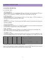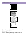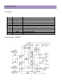
1
S/G No.:TCM500FEF0
Service Manual
Color Television
CHASSIS : CM-500/500F
Model :
DTU-29M5ME/MP/MT/MZ
DTU-29M6ME/MP/MT/MZ
DTU-29M7ME/MP/MT/MZ
DTU-29U1ME/MP/MT/MZ
DTU-29U5ME/MP/MT/MZ
DTU-29U8ME/MP/MT/MZ
DTU-29F1ME/MP/MT/MZ
DTU-29F2ME/MP/MT/MZ
DTU-29F3ME/MP/MT/MZ
MODEL OPTION LIST
MODEL
ME
MP
MT
MZ
TEXT
O
X
O
X
PIP
O
O
X
X
Caution
: In this Manual, some parts can be changed for improving. their
performance without notice in the parts list. So, if you need the
latest parts information, please refer to PPL(Parts Price List)in
Service Information Center.
JULY. 2005
TABLE OF CONTENTS
1. SPECIFICATIONS
2. SAFETY INSTRUCTION
3. CIRCUIT BLOCK DIAGRAM
4. ALIGNMENT INSTRUCTIONS
5. CM-500/F TYPICAL SERVICE DATA
6. ELECTRICAL PARTS LIST
7. EACH MODEL PARTS LIST
8. SCHEMATIC DIAGRAM
9. PRINTED CIRCUIT BOARD
10. MECHANICAL EXPLODED VIEW AND PARTS LIST
2
3
4
5
15
16
24
25
26
29
APPENDIX(Appendix is provide only by internet[http://svc.dwe.co.kr])
11. IC DESCRIPTION
12. TROUBLE SHOOTING GUIDE
38
68
-1-
1. SPECIFICATIONS
Items
Model
TV Standard
Color system
Sound system
Rated Voltage
Power consumption
Sound Output Power
Channel Conerage VHF
UHF
Tuning System
Program No. Indication
Program Selection
Aux. Terminal
Remote Control Unit
Screen size
DTU-29M5ME/MP/MT/MZ
DTU-29M6ME/MP/MT/MZ
DTU-29M7ME/MP/MT/MZ
DTU-29U1ME/MP/MT/MZ
DTU-29U5ME/MP/MT/MZ
DTU-29U8ME/MP/MT/MZ
DTU-29F1ME/MP/MT/MZ
DTU-29F2ME/MP/MT/MZ
DTU-29F3ME/MP/MT/MZ
PAL/SECAM, NTSC-4.43(AV)
B/G, D/K, I, H
AC 110-250V, 50/60Hz
73W(FLAT:110W)
7W+7W (FLAT:7.5W + 7.5W at EQUILIZER CENTER)
BAND I : CH 02 ~ CH04(48.25MHz ~ 62.25MHz)
BAND II : CH05 ~ CH12(175.25MHz ~ 224.25MHz)
CABLE BAND : S01 ~ S03, (69.25MHz ~ 83.25MHz)
S01 ~ S20, (105,25MHz ~ 294.25MHz)
HYPER BAND : S21~S41(303.25 ~ 463.25MHz)
BAND IV, V : CH21 ~ CH69(471.25MHz ~ 855.25MHz)
FS Tuning System
ON-Screen Display
200 Programs
AV1 input <RCA : input, Scart(Option): input, Output>
AV2 input <SIDE> (Model for 29U8 Seriese: FRONT)
DVD1, DVD2
OUTPUT<OPTION:TV OUT or Monitor OUT>
R-49C07
67.6Cm
-2-
2 SAFETY INSTRUCTION
2 SAFETY INSTRUCTION
NOTE : BEFORE SERVICING THIS CHASSIS READ THE “X-RAY RADIATION PRECAUTIONS”,
“SAFETY PRECAUTIONS” AND “PRODUCT SAFETY NOTICE” BELOW.
X-RAY RADIATION PRECAUTION
1. Excessive high voltage can produce potentially hazardous X-RAY RADIATION. To avoid
such hazards, the high voltage must not exceed the specified limit. The nominal value of the
high voltage of this receiver is 25.6KV [Normal Type](27.9KV [Flat Type]) at max beam
current. The high voltage must not, under any circumstances, exceed 28.6KV [Normal Type]
(30.9KV [Flat Type]). Each time a receiver requires servicing, the high voltage should be
checked. It is important to use an accurate and reliable high voltage meter.
2. The only source of X-RAY Radiation in this TV receiver is the picture tube. For continued XRAY RADIATION protection, the replacement tube must be exactly the same type tube as
specified in the parts list.
SAFETY PRECAUTION
1. Potentials of high voltage are present when this receiver is operating. Operation of the
receiver outside the cabinet or with the back cover removed involves a shock hazard from
the receiver.
1) Servicing should not be attempted by anyone who is not thoroughly familiar with the
precautions necessary when working on high voltage equipment.
2) Always discharge the picture tube to avoid the shock harzard before removing the anode
cap.
3) Discharge the high potential of the picture tube before handling the tube. The picture tube is
highly evacuated and if broken, glass fragments will be violently expelled.
2. If any Fuse in this TV receiver is blown, replace it with the FUSE specified in the
Replacement Parts List.
3. When replacing a high wattage resistor (metal oxide film resistor) in the circuit board, keep
the resistor 10 mm away from circuit board.
4. Keep wires away from high voltage or high temperature components.
5. This receiver must operate between AC 110-250 volts, 50/60Hz. NEVER connect to DC
supply or any other power or frequency.
PRODUCT SAFETY NOTICE
Many electrical and mechanical parts in this equipment have special safety-related
characteristics. These characteristics are often passed unnoticed by a visual inspection and the
X-RAY RADIATION protection afforded by them cannot necessarily be obtained by using
replacement components rated for higher voltage, wattage, etc. Replacement parts which have
these special safety characteristics are identified in this manual and its supplements, electrical
components having such features are identified by designated symbol ‘ 1 ’ on the parts list.
Before replacing any of these components, read the parts list in this manual carefully. The use
of substitutes replacement parts which do not have the same safety characteristics as specified
in the parts list may create X-RAY Radiation.
-3-
3.CIRCUIT BLOCK DIAGRAM
-4-
4. ALIGNMENT INSTRUCTIONS
DOCUMENT HISTORY
VERSION
V0.00
V1.00
V1.01
V1.02
DATE
26/10/04
12/11/04
25/11/04
29/11/04
V1.03
02/12/04
V1.04
V1.05
V1.06
17/12/04
20/01/05
16/02/05
COMMENTS
Document imported from project Cp520(Author J.D.Santos)
Major revision after visit in Gunpo RND
Tuner option revision(Byte1, bite2,1,0)
Curtain beep option added(Byte3, bits1)
Curtain ON/OFF bit setting corrected
Local key option bit changed.
Digital eye levels added
Local keyboard option 01 changed
AV stereo and Koran options added
Default setting in case of virgin EEPROM changed
-5-
ALIGNMENT INSTRUCTIONS
4.1MICROCONTROLLER CONFIGURATION : SERVICE MODE
To switch the TV set into service mode please see instruction below.
1 - Select PR. number 91
2 - Adjust sharpness to minimum and exit all menus.
3 - Within 2 seconds press the key sequence : RED - GREEN - menu
The software version is displayed beside the word Service, e.g. “SERVICE V1.00”.
To exit SERVICE menu press menu key or Stand By key.
4.2 SERVICE MODE NAVIGATION
Pr Up/Down remote keys : cycle through the service items available.
Vol -/+ remote keys
: Dec./Increment the values within range - Cycle trough option bits.
OK key
: Toggle bits in option byte
Order
1
2
3
4
5
6
7
8
9
10
11
12
13
14
15
16
17
18
Item
HOR CEN
RED GAIN
GRN GAIN
BLUE GAIN
RED BIAS
GRN BIAS
AGC LEVEL
G2 - SCREEN
OPTION1
OPTION2
OPTION3
V. LINEAR
V. SLOPE
S. CORRECT
VERT CENT
VERT SIZE
BRIGHINESS
SHIPPING
-6-
Default setting
ALIGNMENT INSTRUCTIONS
1 CONTROL BITS
There are two option bytes available (16 bits in all). These option bits are available from
FACTORY and SERVICE mode. First find the OPTION1, OPTION2 or OPTION3 control, and
then use the UP/DOWN and PLUS/MINUS keys on the relevant remote keypad to control the
bits.
The table below shows the three option bytes available.
Default setting in case of virgin EEPROM are shown in light grey.
4.3.1 OPTION1
B7
B6
B5
TOP FASTEXT TUBE
1 Teletext (FLOF)
4:3
OFF
OFF
0
TOP FASTEXT
Teletext (FLOF) TUBE
16:9
ON
ON
4.3.2 OPTION2
B7
1
B6
NEC
remote
control
B5
AV out:
monitor
Fixed to
‘0’
Daewoo
Remote
control
0
4.3.3 OPTION3
B7
1
B6
AV out:
Tuner
B5
B4
B3
Teletext
ON
Dolby
Virtual
OFF
Teletext
OFF
Dolby
Virtual
ON
B4
B3
Koran
functions
enabled
Koran
functions
enabled
B4
Teletext language table
0
Curtain
On
-7-
B1
Chassis
with E/W
correction
circuit
Chassis
with out
E/W
correction
circuit
B0
TUNER OPTIONS
(see table below)
B2
Local key option
(see table below)
B3
Curtain
OFF
B2
B2
B1
B0
Digital
eye
disabled
PARS
logo
OFF
Digital
eye
enabled
ON
B1
B0
PIP
OFF
Beep at
curtain
opening:
OFF
Full
stereo
PIP
ON
Beep at
curtain
opening:
ON
AV
Stereo
only
ALIGNMENT INSTRUCTIONS
4.4 USER GUIDE
4.4.1 ENTERING FACTORY MODE
To switch the TV set into FACTORY mode, use the factory remote control, and press on “SVC”.
The factory menu will appear on the screen, showing “FACTORY Vx,xx”(where x.xx is the
software version).
4.4.2 ENTERING OPTION BITS MENU
To find the option bits, push the button “OPT” once. To find OPTION2 press the button “OPT” a
second time.
4.4.3 SELECTING OPTION BITS
From left to right, bits 7 to 0 are shown. Navigation is done from the with FACTORY remocon
with the VOL MIN and VOL MAX buttons(otherwise known as EAST, WEST). The selected bit is
highlighted.
4.4.4 TOGGLING OPTION BITS
This is done by using the PR UP and PR DOWN button (otherwise known as NORTH,
SOUTH).
4.4.5 EXTING OPTION BITS MENU
Push the button “OPT” a third time. The full sequence enter to exit is;
FACTORY -> OPTION1 -> OPTION2 -> OPTION3 -> FACTORY
4.4.6 AFTER SETTING OPTION BITS
Before pushing on the shipping key, “BRI.”, it is necessary to push the “NORMAL” key to obtain
NORMAL I. This will reset all the sound and brightness settings to a factory defined level, as
well as some other settings such as sound PRESET and WAKE TIME/PROG.
Then, on pushing the shipping key, thess levels are memorised in the television, ready for
packing and delivery.
4.4.7 VERIFICATION
On pushing the shipping “BRI.” key, a four digit hexadecimal number is displayed in addition to
“SHIPPING”. This number is there to verify the option bits setting that has been entered. For
example the binary code 1001 1111(OPTION3) 0000 0111(OPTION2) 1100 0010(OPTION1)
will give 9F 07 C2 hex. The order of display is therefore OPTION3, OPTION2 then OPTION1
when reading from left to right.
-8-
ALIGNMENT INSTRUCTIONS
4.5 CONTROL DESCRIPTION
4.5.1 OPTION 1 BITS
- TOP Teletext(Bit 7)
Enables/disables the TV from displaying TOP row 24 link titles, and the dedicated TOP menu
table. A FLOF (if available) or SIMPLE / PAGETRACE presentation will be used.
- FLOF/Fastext (Bit 6)
Enables/disables the TV from displaying FLOF row 24 link titles. A TOP(if available) or
SIMPLE/PAGETRACE presentation will be used.
- Tube(Bit 5)
Define as 4:3 or16:9 tube. This will permit the ZOOM function to understand the formats that
should be available.
- Teletext ON/OFF(Bit 4)
Enables/disables the Teletext on TV. If Teletext is disabled, user can not select clock prog and
zoom selection in features menu. WSS is also disabled.
- Dolby Virtual(Bit 3)
Allows Doby Virtual (trademark) 3D effect to be available from the user control(button “3D”).
Note : Dolby Virtual is only available with some UOC reference.
- Tuner(Bits 2,1 & 0)
Configures the software to communicate with the tuner via i2c bus. Incorrect configuration may
not be immediately obvious, but will result in loss of functionality (e.g. unable to tune UHF
Bit2
0
0
0
0
1
1
Bit1
0
0
1
1
0
0
Bit0
0
1
0
1
0
1
LAN
No
No
No
No
Yes
Yes
Tuner
Philips (external AGC)
Philips (internal AGC)
Alps
Partsnic or Samsung
Philips UV1356A MK3 (external AGC)
Philips UV1356A MK3 (internal AGC)
channels, unable to tune some hyperband channels).
See also NVM mapping to configure parameters for automatic AGC adjustment when external
AGC is used. When internal AGC is used, the TOP is stored in NVM.
-9-
ALIGNMENT INSTRUCTIONS
4.5.2 OPTION 2 BITS
- Remote control(Bit 7)
This is not intended to be changed by use of the FACTORY remote control.
- NEC/Daewoo Remocon(Bit 6)
User remote control configuration, the choise being between the following;
- NEC remocon(‘1’)
- Daewoo R-49C07(‘0’)
The R-30SVC7 “FACTORY” remote control will never be affected by this setting.
- Local keyboard option (Bit 3 & 2)
0 mV ~ 220 mV
22 mV ~ 620 mV
620 mV ~ 1.06 V
1.06 V ~ 1.48 V
1.48 V ~ 1.79 V
1.79 V ~ 2.07 V
11
Not used
(TV/AV) Menu
Vol. Up
Vol. Dwn
Prog.Up
Prog.Dwn
10
Menu
TV/AV
Vol. Dwn
Vol. Up
Prog. Dwn
Prog. Up
01
Menu
Prog. Up
Prog. Dwn
Vol. Up
Vol. Dwn
TV/AV
00
Not used
- Digital eye ON/OFF(Bit 1)
Enables/disables the digital eye function.
When enabled and selected, the microcontroller measures DC level on IC pin 15, and adjusts
picture setting according to the table below.
0 mV ~ 450 mV
450 mV ~ 900 mV
900 mV ~ 1.35 V
1.35 V ~ 1.80 V
1.80 V ~ 2.25 V
2.25 V ~ 2.70 V
Brightness
18
28
30
32
34
36
Contast
30
46
50
55
60
63
Colour
28
28
29
30
31
32
Sharpness
27
29
30
31
32
33
- PARS Logo ON/OFF(Bit 0)
Enables/disables the display of PARS logo at power on.
4.5.3 OPTION 3 BITS
- Curtain function at power ON(Bit 7)
Enables/disables the curtain function at power ON. The frequency and volume of associated
beep sound is controlled by NVM data.
-10-
ALIGNMENT INSTRUCTIONS
- Teletext language option(Bit 6, 5&4)
Latin West
Latin East
Russia
Persia
Arabic
Not used
..
Not used
Bit6, 5&4
000
001
010
011
100
101
111
Teletext National Option table for each language option:
Teletext table C12 C13 C14
Latin West
Latin East
Russian
Arabic/
Persian
0
0
0
0
1
1
1
1
0
0
0
0
1
1
1
1
0
0
0
0
1
1
1
1
0
0
0
0
1
1
1
1
0
0
1
1
0
0
1
1
0
0
1
1
0
0
1
1
0
0
1
1
0
0
1
1
0
0
1
1
0
0
1
1
0
1
0
1
0
0
0
1
0
1
0
1
0
1
0
1
0
1
0
1
0
1
0
1
0
1
0
1
0
1
0
1
Basic Char.Set Twist Char.Set
Latin
Latin
Latin
Latin
Latin
Latin
Latin
Latin
Latin
Latin
Latin
Latin
Latin
Latin
Latin
Latin
Latin
Latin
Latin
Latin
Cyrillic
Cyrillic
Latin
Latin
Latin
Latin
Latin
Latin
Latin
Latin
Latin
Arabic
Latin
Latin
Latin
Latin
Latin
Latin
Latin
Latin
Latin
Latin
Latin
Latin
Latin
Latin
Latin
Latin
Latin
Latin
Latin
Latin
Latin
Latin
Latin
Latin
Latin
Latin
Latin
Latin
Latin
Latin
Latin
Latin
NOT
EW
English
German
Swedish/Fin
Italian
French
Spanish/Portuguese
Turkish
English
Polish
German
Estontan
German
German
Slovenian
Czech/Slovak
Rumanian
English
German
Estonian
German
Russia
Ukrainian
Czech/Slovak
Rumanian
English
German
Swedish/Fin
Italian
French
Spanish/Portuguese
Turkish
Arabic
West
West
West
West
West
West
West
West
East
East
East
East
East
East
East
East
West
West
East
East
East
East
East
East
West
West
West
West
West
West
West
West
- East/West correction (Bit 3)
You must enable this bit for large screen CRT which need EAST WEST correction circuitry.
- PIP(Bit 2)
Enable disable PIP function. Make sure PIP board is inserted in the main board.
- Beep at curtain opening(Bit 1)
Enable/disable beep sound at power ON.
-11-
ALIGNMENT INSTRUCTIONS
4.5.4 TV SET ALIGNMENT
(1) G2 ALIGNMENT
- Tune a colour bar pattern.
- Fine the “G2-SCREEN” item in service mode.
- Adjust screen volume(on FBT) to make the horizontal line just before disappeared.
(2) WHITE BALANCE
- Select a dark picture and adjust RED BIAS and GRN BIAS to the desired colour temperature.
- Select a bright picture and adjust RED, GRN and BLUE GAIN to the desired colour temperature.
(3) FOCUS
Adjust the Focus volume ( on FBT ) to have the best resolution on screen.
(4) VERTICAL GEOMETRY
Adjust V. LINEAR (linearity), S CORRECT (S. Correction), VERT SIZE (Vertical amplitude), VERT CENT (vertical
centring) to compensate for vertical distortion.
(5) HORIZONTAL PICTURE CENTRING
Adjust HOR CEN (Horizontal centre) to have the picture in the centre of the screen.
(6) EAST / WEST CORRECTION
Adjust the PARABOLA, HOR WIDTH, CORNER, HOR PARAL, EW TRAPEZ, to compensate for geometrical
distortion.
HOR PARAL
-12-
ALIGNMENT INSTRUCTIONS
HOR WIDTH
adjust for 90% overscan.
PARABOLA
CORNER B & CORNER T
EW TRAPEZ
3.7.7 AGC
- Make sure option bits are correct for the tuner fitted on the chassis (See above how to change option bits).
- Adjust the antenna signal level at 62 dB V± 2
- Tune a colour bar pattern.
- Find the “AGC LEVEL” item in service mode.
- Press the key “OK” on the remote keypad and wait until AGC level stabilise to the optimum value.
- Alternatively, use “Vol Up/Dwn” keys to adjust manually to the desired Tuner Take Over Point (TOP).
-13-
ALIGNMENT INSTRUCTIONS
Remote control
TELETEXT MODE
TV MODE
POWER
SOUND MUTE
NUMBER 0..9
POWER
SOUND MUTE
NUMBER 0..9
TV / AV
NORMAL
RECALL
MENU
PROGRAM UP (CURSOR UP)
VOLUME DOWN (CURSOR LEFT)
VOLUME UP (CURSOR RIGHT)
PROGRAM DOWN (CURSOR
DOWN)
MODE
OK / PRESET
PIP ON
PIP PICTURE SWAP
PIP POSITION
PIP PICTURE SOURCE
TV
VOL/BRIGHT MENU SELECTION
PAGE UP
VOL / BRIGHT DOWN
VOL / BRIGHT UP
PAGE DOWN
INDEX
RED
GREEN
YELLOW
CYAN
CANCEL
PAGE HOLD
TELETEXT TV
REVEAL
SUBPAGE
HEIGHT
TELETEXT
PIP PICTURE SIZE
SLEEP
ZOOM
3D (SOUND EFFECT)
-14-
5. CM-500/F TYPICAL SERVICE DATA
-15-
6. ELECTRICAL PARTS LIST
LOC
PART CODE
ZZ100
48B5849C07
ZZ110
PTACPWE135
30
4850Q00910
200
48586054K1
M821
4858213803
ZZ120
PTBCSHE135
M211
4852161121
M781
4857817630
ZZ130
PTPKCPE135
10
6520010100
M801
4858057600
M811
4858199100
M821
4858215601
ZZ131
48519A7810
ZZ132
58G0000182
ZZ140
PTCACAE135
M201A
4856017350
M201B
4856215402
M211A
7172401612
M211B
7172401612
M211C
7178301212
M231A
7172401612
M541
4855419800
M682
4856816300
M683
4856812001
SP01A
7172401212
SP02A
7172401212
V901
4859646261
ZZ200
PTFMSJE135
M201
4852079701
M231A
7178301212
M561
48556293SD
M781
4857821102
ZZ205
PTPCSWJ912
M191
4851945700
M191A
7178301011
M231
4852328201
M481
4854861401
M481A
4856716000
M591
4855933401
M591A
7178301011
ZZ210
PTSPPWD703
P601A
4850704S32
SP01
4858311110
SP02
4858311110
ZZ290
PTMPMSE135
C310
CEYD1H689W
C405
CMYH3C103J
C406
CMYH3C912J
C408
CMYE2D624J
C424
CEYF2A471V
C801
CL1UC3474M
C811
CH1BFE222M
C817
CEYF2C221V
C821
CEYF1E222V
C850
CEYD2G221D
D402
DRGP30J—D403
DDGP30L—D812
DRGP30J—D814
DSR306E20DF01
DLH2PR——
F801
5F3GB6322L
H01
485A101880
H02
485A101980
I301
PTC2SW8227
11TDA8358J-IC VERTICAL
0000A
4857028227
0000B
7174301011
PART NAME
DESCRIPTION
TRANSMITTER REMOCON
ACCESSORY AS
BATTERY
MANUAL INSTRUCTION
BAG INSTRUCTION
COVER BACK AS
COVER BACK
CLOTH BLACK
PACKING AS
STAPLE PIN
BOX CARTON
PAD
BAG P.E
CRT GROUND NET
COIL DEGAUSSING
CABINET AS
SCREW CRT FIX
WASHER RUBBER
SCREW TAPPTITE
SCREW TAPPTITE
SCREW TAPPTITE
SCREW TAPPTITE
SPEC PLATE
CLAMP WIRE
TIE CABLE
SCREW TAPPTITE
SCREW TAPPTITE
CRT
MASK FRONT AS
MASK FRONT
SCREW TAPPTITE
MARK BRAND
CLOTH BLACK
PANEL CONTROL AS
BUTTON CTRL
SCREW TAPPTITE
PANEL DECO
BUTTON POWER
SPRING
DECO EYE
SCREW TAPPTITE
SPEAKER AS
CONNECTOR
SPEAKER
SPEAKER
PCB MAIN MANUAL AS
C ELECTRO
C MYLAR
C MYLAR
C MYLAR
C ELECTRO
C LINE ACROSS
C CERA AC
C ELECTRO
C ELECTRO
C ELECTRO
DIODE
DIODE
DIODE
DIODE
LED BLOCK
FUSE GLASS TUBE
WIRE
WIRE
HEAT SINK ASS`Y
TDA8358J
HEAT SINK
SCREW TAPPTITE
R-49C07 (AAA)
DTU-29M5ME
R03/NN
DTM-2082CW
L.D.P.E TO.05X250X400(+20)
DTU-29M5ME
HIPS GY
FELT 400X20X0.7
DTU-29M5ME
AUTO W65
DW-3
EPS 29M5
PE FOAM t0.5x1600x1270
2903S-1015-1P
DC-29SF AL
DTU-29M5ME
6X27 L120 BK
CR T2.0
TT2 TRS 4X16 MFZN BK
TT2 TRS 4X16 MFZN BK
TT2 WAS 3X12 MFZN BK
TT2 TRS 4X16 MFZN BK
ART 150
NYLON 6 (V0)
NYLON66 DA100
TT2 TRS 4X12 MFZNBK
TT2 TRS 4X12 MFZNBK
A68KTB359X001(P) P38
DTU-29M5ME
HIPS GY
TT2 WAS 3X12 MFZN BK
SILVER DIA-CUTTING
FELT 340X10X1.5
DTQ-29M5
4951401+5545800
TT2 WAS 3X10 MFZN
ABS GY
ABS GY
SWPA PIE0.5
ABS BLUE
TT2 WAS 3X10 MFZN
DTC-29M5ME
YH025-04+YRT205+ULW=900
12W 8 OHM SP-58126F
12W 8 OHM SP-58126F
DTU-29M5ME
50V RHD 6.8MF (16X35.5)
1.6KV BUP 0.01MF J
1.6KV BUP 9100PF J
200V PU 0.62MF J
100V RSS 470MF (16X31.5)
0.47MF 1J(UCVSNDF/SV)+Q/O
U/C/V AC400V 2200PF
160V RSS 220MF (18X35.5)
25V RSS 2200MF (16X25)
400V FHS 220MF (25X40)
RGP30J DO-201AD 600V 3A
DGP30L
RGP30J DO-201AD 600V 3A
SR306E20
LH-2P-R
V/S TL 6.3A 250V MF51
1007AWG26=100
1007AWG26=180
1TDA8358J- + 7174301011
AL EX BK
TT2 RND 3X10 MFZN
REMARK
LOC
PART CODE
I601
PTA2SW8232
11LA42152-EIC AUDIO AMP
0000A
4857028232
0000B
7174301011
I701
1DA12072PQ
I702
124LC16B1B
I801
PTA2SW7924
11STRW67560000A
4857027924
0000B
7174300811
I802
1LTV817C—
I804
PTT2SW6902
11LD1117V33
0000A
4857026902
0000B
7174300811
I805
PTJ2SW7802
11K78R05—-IC REGULATOR
0000A
4857027802
0000B
7174300811
IF01
1346VF6—JPA01
4859110950
JPA02
4859111750
L301
58C7070085
L401
58H0000066
LF801
5PLF28A1—
M687
4853747800
PW801
4859903110
A000
4859903511
Q401
PTG2SW7609
1TST2009DH1
0000A
4857027609
0000B
7174300811
Q402
TKTC3229—
R801
DDC7R0M290
R803
RX10T339JS
SW801
5S40101143
T401
50H0000294
T402
5TD0000018
T801
50M4445B9TU01
4859724930
X701
5XJ24R576E
Z701
5PK3953M—
Z702
5PK9650M—
ZZ200
PTMPJ0E135
C407
CMXE2G273J
C409
CEXF2C339V
C421
CCXB3D681K
C422
CEXF2C101V
C423
CMXE2J472J
C427
CEXF1E471V
C613
CEXF1E222V
C803
CCXB3A472K
C804
CCXB3A472K
C806
CCXB3D471K
C813
CCXB3D471K
C818
CEXF2C101V
C820
CEXF1E222V
C824
CMXB2G122J
C835
CEXF1C471V
C838
CEXF1C102V
ZZ200
PTMPJBE135
10
2TM18006BE
E001
4856310300
E002
4856310300
E003
4856310300
E004
4856310300
E005
4856310600
E006
4856310600
-16-
PART NAME
DESCRIPTION
HEAT SINK ASS`Y
LA42152-E
HEAT SINK
SCREW TAPPTITE
IC
IC MEMORY
HEAT SINK ASS`Y
IC POWER
HEAT SINK
SCREW TAPPTITE
IC PHOTO COUPLER
HEAT SINK ASS`Y
IC REGULATOR
HEAT SINK
SCREW TAPPTITE
HEAT SINK ASS`Y
KIA78R05API
HEAT SINK
SCREW TAPPTITE
IC PREAMP
JACK PIN BOARD
JACK PIN BOARD
COIL CHOKE
COIL H-LINEARITY
FILTER LINE
RETA PCB
CORD POWER AS
CORD POWER
HEAT SINK ASS`Y
TR HORI
HEAT SINK
SCREW TAPPTITE
TR
POSISTOR
R CEMENT
SW POWER PUSH
FBT
TRANS DRIVE
TRANS SMPS
TUNER VARACTOR
CRYSTAL QUARTZ
FILTER SAW
FILTER SAW
PCB MAIN (RHU) AS
C MYLAR
C ELECTRO
C CERA
C ELECTRO
C MYLAR
C ELECTRO
C ELECTRO
C CERA
C CERA
C CERA
C CERA
C ELECTRO
C ELECTRO
C MYLAR
C ELECTRO
C ELECTRO
PCB MAIN M-10 AS
TAPE MASKING
EYE LET
EYE LET
EYE LET
EYE LET
EYE LET
EYE LET
1LA42152-E + 7174301011
AL EX BK
TT2 RND 3X10 MFZN
TDA12072PQ/N1D
24LC16B1B
1STRW6756- + 7174300811
STR-W6756
AL EX
TT2 RND 3X8 MFZN
LTV-817C
1LD1117V33 + 7174300811
LD1117AV33 3.3V 2% TO-220
AL EX BK
TT2 RND 3X8 MFZN
1K78R05—- + 7174300811
AL EX
TT2 RND 3X8 MFZN
346VF6
YS01-0001
PH-JB-9515
TLN-3062A
TRL-230D
LF-28A1
NYLON 66
KKP-419J-H03VVH2+H0U=2200
CW4232 H03VVH2-F=2250
TST2009DH1 + 7174300811
ST2009DHI
AL EX
TT2 RND 3X8 MFZN
KTC3229
ECPCD7R0M290
10W 3.3 OHM J TRIPOD SMALL
PS3-22SP (P.C.B)
LTC-432
THD-120
TSM-4445B9
UV1316/A I-4
HC-49/S 24.576MHZ 30PPM
K3953M
K9650M
DTU-29M5ME
400V PU 0.027MF J (TP)
160V RSS 3.3MF (8X16) TP
2KV B 680PF K (TAPPING)
160V RSS 100MF (16X25) TP
630V PU 4700PF J (TP)
25V 470MF 10X12.5
25V RSS 2200MF (16X25) TP
1KV B 4700PF K (TAPPING)
1KV B 4700PF K (TAPPING)
2KV B 470PF K (TAPPING)
2KV B 470PF K (TAPPING)
160V RSS 100MF (16X25) TP
25V RSS 2200MF (16X25) TP
400V EU 1200PF J
16V RSS 470MF (8X12)TP
16V RSS 1000MF (10X20) TP
DTU-29M5ME
6.2X500
BSR T0.2 (R1.6)
BSR T0.2 (R1.6)
BSR T0.2 (R1.6)
BSR T0.2 (R1.6)
BSR T0.2 (R2.3)
BSR T0.2 (R2.3)
REMARK
ELECTRICAL PARTS LIST
LOC
PART CODE
PART NAME
DESCRIPTION
E007
E008
E009
E010
E011
E012
E013
E014
E018
E019
E020
E021
E022
E023
E024
E025
E026
E027
E028
E029
E030
E031
E032
E033
E034
E035
E036
E037
E038
E039
E040
E042
E043
E044
E045
E046
E047
E048
E049
E050
E051
E059
E060
E065
E066
E067
E068
E069
E070
E080
E081
N0010
N0011
N0012
N0013
N005
N006
N007
N008
P402
P501
P601
P602
P603
P701
PD01
R310
R317
4856310300
4856310300
4856310300
4856310300
4856310600
4856310600
4856310600
4856310600
4856310300
4856310300
4856310300
4856310300
4856310600
4856310600
4856310600
4856310600
4856310300
4856310300
4856310300
4856310300
4856310300
4856310600
4856310600
4856310300
4856310300
4856310300
4856310600
4856310600
4856310600
4856310600
4856310300
4856310300
4856310600
4856310600
4856310600
4856310600
4856310600
4856310300
4856310300
4856310600
4856310600
4856310600
4856310600
4856310600
4856310600
4856310600
4856310600
4856310600
4856310600
4856310600
4856310600
4857417500
4857417500
4857417500
4857417500
4857417500
4857417500
4857417500
4857417500
485923182S
485923202S
485923172S
485923182S
485923192S
485923172S
485923162S
RS02Z129JS
RS02Z100JS
EYE LET
EYE LET
EYE LET
EYE LET
EYE LET
EYE LET
EYE LET
EYE LET
EYE LET
EYE LET
EYE LET
EYE LET
EYE LET
EYE LET
EYE LET
EYE LET
EYE LET
EYE LET
EYE LET
EYE LET
EYE LET
EYE LET
EYE LET
EYE LET
EYE LET
EYE LET
EYE LET
EYE LET
EYE LET
EYE LET
EYE LET
EYE LET
EYE LET
EYE LET
EYE LET
EYE LET
EYE LET
EYE LET
EYE LET
EYE LET
EYE LET
EYE LET
EYE LET
EYE LET
EYE LET
EYE LET
EYE LET
EYE LET
EYE LET
EYE LET
EYE LET
TERM PIN
TERM PIN
TERM PIN
TERM PIN
TERM PIN
TERM PIN
TERM PIN
TERM PIN
CONN WAFER
CONN WAFER
CONN WAFER
CONN WAFER
CONN WAFER
CONN WAFER
CONN WAFER
R M-OXIDE FILM
R M-OXIDE FILM
BSR T0.2 (R1.6)
BSR T0.2 (R1.6)
BSR T0.2 (R1.6)
BSR T0.2 (R1.6)
BSR T0.2 (R2.3)
BSR T0.2 (R2.3)
BSR T0.2 (R2.3)
BSR T0.2 (R2.3)
BSR T0.2 (R1.6)
BSR T0.2 (R1.6)
BSR T0.2 (R1.6)
BSR T0.2 (R1.6)
BSR T0.2 (R2.3)
BSR T0.2 (R2.3)
BSR T0.2 (R2.3)
BSR T0.2 (R2.3)
BSR T0.2 (R1.6)
BSR T0.2 (R1.6)
BSR T0.2 (R1.6)
BSR T0.2 (R1.6)
BSR T0.2 (R1.6)
BSR T0.2 (R2.3)
BSR T0.2 (R2.3)
BSR T0.2 (R1.6)
BSR T0.2 (R1.6)
BSR T0.2 (R1.6)
BSR T0.2 (R2.3)
BSR T0.2 (R2.3)
BSR T0.2 (R2.3)
BSR T0.2 (R2.3)
BSR T0.2 (R1.6)
BSR T0.2 (R1.6)
BSR T0.2 (R2.3)
BSR T0.2 (R2.3)
BSR T0.2 (R2.3)
BSR T0.2 (R2.3)
BSR T0.2 (R2.3)
BSR T0.2 (R1.6)
BSR T0.2 (R1.6)
BSR T0.2 (R2.3)
BSR T0.2 (R2.3)
BSR T0.2 (R2.3)
BSR T0.2 (R2.3)
BSR T0.2 (R2.3)
BSR T0.2 (R2.3)
BSR T0.2 (R2.3)
BSR T0.2 (R2.3)
BSR T0.2 (R2.3)
BSR T0.2 (R2.3)
BSR T0.2 (R2.3)
BSR T0.2 (R2.3)
DA-IB0214(D2.3/DY PIN)
DA-IB0214(D2.3/DY PIN)
DA-IB0214(D2.3/DY PIN)
DA-IB0214(D2.3/DY PIN)
DA-IB0214(D2.3/DY PIN)
DA-IB0214(D2.3/DY PIN)
DA-IB0214(D2.3/DY PIN)
DA-IB0214(D2.3/DY PIN)
YW025-05 (STICK)
YW025-07 (STICK)
YW025-04 (STICK)
YW025-05 (STICK)
YW025-06 (STICK)
YW025-04 (STICK)
YW025-03 (STICK)
2W 1.2 OHM J SMALL
2W 10 OHM J SMALL
REMARK
LOC
PART CODE
R403
R404
R406
R407
R408
R409
R414
R419
R422
R807
R813
R830
ZZ200
C102
C104
C106
C128
C130
C301
C305
C306
C313
C314
C402
C403
C410
C411
C412
C413
C414
C416
C425
C601
C602
C603
C604
C605
C606
C607
C608
C609
C610
C614
C701
C704
C707
C713
C716
C721
C722
C723
C726
C727
C730
C731
C732
C734
C735
C740
C749
C751
C752
C753
C754
C755
C756
C758
C759
RS01Z272JRS02Z101JS
RS02Z203JS
RS02Z102JS
RF01Z100JRS01Z103JRS02Z203JS
RS02Z201JS
85801060GY
RF02Z188KRF02Z688KRS02Z104JS
PTMPJRE135
CEXF1C100V
CEXF1H101V
CEXF1H101V
CEXF1H229V
CEXF1C101V
CMXM2A393J
CMXL1J104J
CMXL1J104J
CMXM2A473J
CMXM2A473J
CCXB2H222K
CMXM2A103J
CCXB2H561K
CEXF2E229V
CCXB2H221K
CMXL1J104J
CMXM2A473J
CCXB2H102K
CCXB2H102K
CEXF1E470V
CMXL1J224J
CMXL1J224J
CEXF1H100V
CCXB1H682K
CCXB1H682K
CMXM2A104J
CMXM2A104J
CMXM2A104J
CMXM2A104J
CEXF1C470V
CEXF1C101V
CEXF1E470V
CEXF1C101V
CEXF1C470V
CEXF1C101V
CEXF1C101V
CMXL1J224J
CEXF1H229V
CMXL1J104J
CEXF1C101V
CEXF1C101V
CEXF1E470V
CMXL1J224J
CMXL1J224J
CEXF1C101V
CEXF1C101V
CEXF1C101V
CMXL1J104J
CMXM2A104J
CMXL1J104J
CMXL1J154J
CEXF1H109V
CEXF1H100V
CMXL1J224J
CMXM2A682J
-17-
PART NAME
DESCRIPTION
R M-OXIDE FILM
R M-OXIDE FILM
R M-OXIDE FILM
R M-OXIDE FILM
R FUSIBLE
R M-OXIDE FILM
R M-OXIDE FILM
R M-OXIDE FILM
WIRE COPPER
R FUSIBLE
R FUSIBLE
R M-OXIDE FILM
PCB MAIN RADIAL AS
C ELECTRO
C ELECTRO
C ELECTRO
C ELECTRO
C ELECTRO
C MYLAR
C MYLAR
C MYLAR
C MYLAR
C MYLAR
C CERA
C MYLAR
C CERA
C ELECTRO
C CERA
C MYLAR
C MYLAR
C CERA
C CERA
C ELECTRO
C MYLAR
C MYLAR
C ELECTRO
C CERA
C CERA
C MYLAR
C MYLAR
C MYLAR
C MYLAR
C ELECTRO
C ELECTRO
C ELECTRO
C ELECTRO
C ELECTRO
C ELECTRO
C ELECTRO
C MYLAR
C ELECTRO
C MYLAR
C ELECTRO
C ELECTRO
C ELECTRO
C MYLAR
C MYLAR
C ELECTRO
C ELECTRO
C ELECTRO
C MYLAR
C MYLAR
C MYLAR
C MYLAR
C ELECTRO
C ELECTRO
C MYLAR
C MYLAR
1W 2.7K OHM J (TAPPING)
2W 100 OHM J SMALL
2W 20K OHM J SMALL
2W 1K OHM J SMALL
1W 10 OHM J (TAPPING)
1W 10K OHM J (TAPPING)
2W 20K OHM J SMALL
2W 200 OHM J SMALL
1/0.6 TIN COATING
2W 0.18 OHM K (TAPPING)
2W 0.68 OHM K (TAPPING)
2W 100K OHM J SMALL
DTU-29M5ME
RSS 16V 10MF 4X7
50V RSS 100MF (8X11.5) TP
50V RSS 100MF (8X11.5) TP
50V RSS 2.2MF (5X11) TP
16V RSS 100MF (6.3X11) TP
100V 0.039MF J (TP)
63V MEU 0.1MF J
63V MEU 0.1MF J
100V 0.047MF J (TP)
100V 0.047MF J (TP)
500V B 2200PF K (TAPPING)
100V 0.01MF J (TP)
500V B 560PF K (TAPPING)
250V RSS 2.2MF (8X11.5)TP
500V B 220PF K (TAPPING)
63V MEU 0.1MF J
100V 0.047MF J (TP)
500V B 1000PF K (TAPPING)
500V B 1000PF K (TAPPING)
RSS 25V 47MF 5X11 P5.0 TA
63V MEU 0.22MF J (TP)
63V MEU 0.22MF J (TP)
50V RSS 10MF (5X11) TP
50V B 6800PF K (TAPPING)
50V B 6800PF K (TAPPING)
100V 0.1MF J (TP)
100V 0.1MF J (TP)
100V 0.1MF J (TP)
100V 0.1MF J (TP)
16V RSS 47MF (5X11) TP
16V RSS 100MF (6.3X11) TP
RSS 25V 47MF 5X11 P5.0 TA
16V RSS 100MF (6.3X11) TP
16V RSS 47MF (5X11) TP
16V RSS 100MF (6.3X11) TP
16V RSS 100MF (6.3X11) TP
63V MEU 0.22MF J (TP)
50V RSS 2.2MF (5X11) TP
63V MEU 0.1MF J
16V RSS 100MF (6.3X11) TP
16V RSS 100MF (6.3X11) TP
RSS 25V 47MF 5X11 P5.0 TA
63V MEU 0.22MF J (TP)
63V MEU 0.22MF J (TP)
16V RSS 100MF (6.3X11) TP
16V RSS 100MF (6.3X11) TP
16V RSS 100MF (6.3X11) TP
63V MEU 0.1MF J
100V 0.1MF J (TP)
63V MEU 0.1MF J
63V MEU 0.15MF J
50V RSS 1MF (5X11) TP
50V RSS 10MF (5X11) TP
63V MEU 0.22MF J (TP)
100V 6800PF J (TP)
REMARK
ELECTRICAL PARTS LIST
LOC
PART CODE
C761
C765
C766
C767
C768
C770
C771
C772
C780
C781
C783
C784
C790
C805
C807
C808
C810
C812
C814
C819
C822
C825
C828
C836
C840
C860
C870
CD01
CD03
CV01
CV02
CV03
F801A
F801B
I803
L302
L303
L601
L812
Q101
Q403
Q602
Q701
Q704
Q705
Q706
Q707
Q708
Q721
Q722
Q810
Q852
Q853
QF01
R319
R426
R613
R614
R615
R616
SW701
SW702
SW703
SW704
SW705
SW706
ZZ200
10
CCXB1H101K
CEXF1H229V
CEXF1H229V
CMXL1J104J
CEXF1H229V
CEXF1C101V
CEXF1H478V
CEXF1H478V
CMXL1J104J
CMXL1J104J
CEXF1C100V
CEXF1C101V
CEXF1H479V
CEXF1H100V
CCXB1H821K
CCXB1H471K
CEXF1H109V
CCXR3A102K
CCXB3A271K
CEXF2A100V
CMXM2A102J
CCXF1H473Z
CEXF1C101V
CMXM2A104J
CEXF1H229V
CEXF1H330V
CEXF1C101V
CEXF1C470V
CEXF1C470V
CEXF1H478V
CEXF1H478V
CMXL1J104J
4857415001
4857415001
1K1A431B—
58C0000142
58C0000142
58C0000142
58C0000142
TKTC3198YTKTA1266YTKTA1266YTKTA1266YTKTC3198YTKTA1270YTKTC3198YTKTA1270YTKTC3198YTH2N7000—
TH2N7000—
TKSA1013YTKTC3198YTKTC3198YTKTC3198YRN02B181JS
RN02B222JS
RN01B229JS
RN01B229JS
RN01B229JS
RN01B229JS
5S50101090
5S50101090
5S50101090
5S50101090
5S50101090
5S50101090
PTMPJAE135
2TM14006LB
PART NAME
DESCRIPTION
C CERA
C ELECTRO
C ELECTRO
C MYLAR
C ELECTRO
C ELECTRO
C ELECTRO
C ELECTRO
C MYLAR
C MYLAR
C ELECTRO
C ELECTRO
C ELECTRO
C ELECTRO
C CERA
C CERA
C ELECTRO
C CERA
C CERA
C ELECTRO
C MYLAR
C CERA
C ELECTRO
C MYLAR
C ELECTRO
C ELECTRO
C ELECTRO
C ELECTRO
C ELECTRO
C ELECTRO
C ELECTRO
C MYLAR
CLIP FUSE
CLIP FUSE
IC REGULATOR(SHUNT)
COIL CHOKE
COIL CHOKE
COIL CHOKE
COIL CHOKE
TR
TR
TR
TR
TR
TR
TR
TR
TR
FET
FET
TR
TR
TR
TR
R METAL FILM
R METAL FILM
R METAL FILM
R METAL FILM
R METAL FILM
R METAL FILM
SW TACT
SW TACT
SW TACT
SW TACT
SW TACT
SW TACT
PCB MAIN AXIAL AS
TAPE MASKING
50V B 100PF K (TAPPING)
50V RSS 2.2MF (5X11) TP
50V RSS 2.2MF (5X11) TP
63V MEU 0.1MF J
50V RSS 2.2MF (5X11) TP
16V RSS 100MF (6.3X11) TP
50V RSS 0.47MF (5X11) TP
50V RSS 0.47MF (5X11) TP
63V MEU 0.1MF J
63V MEU 0.1MF J
RSS 16V 10MF 4X7
16V RSS 100MF (6.3X11) TP
50V RSS 4.7MF (5X11) TP
50V RSS 10MF (5X11) TP
50V B 820PF K (TAPPING)
50V B 470PF K (TAPPING)
50V RSS 1MF (5X11) TP
HIKR 1KV 1000PF K 125C
1KV B 270PF K (TAPPING)
100V RSS 10MF (6.3X11) TP
100V 1000PF J (TP)
50V F 0.047MF Z (TAPPING)
16V RSS 100MF (6.3X11) TP
100V 0.1MF J (TP)
50V RSS 2.2MF (5X11) TP
50V RSS 33MF (6.3X11) TP
16V RSS 100MF (6.3X11) TP
16V RSS 47MF (5X11) TP
16V RSS 47MF (5X11) TP
50V RSS 0.47MF (5X11) TP
50V RSS 0.47MF (5X11) TP
63V MEU 0.1MF J
PFC5000-0702
PFC5000-0702
KIA431B 2.495V 0.5% TO-92
ELC 0809 940K
ELC 0809 940K
ELC 0809 940K
ELC 0809 940K
KTC3198Y
KTA1266Y (TP)
KTA1266Y (TP)
KTA1266Y (TP)
KTC3198Y
KTA1270Y (TP)
KTC3198Y
KTA1270Y (TP)
KTC3198Y
H2N7000
H2N7000
KSA1013Y (TP)
KTC3198Y
KTC3198Y
KTC3198Y
2W 180 OHM J SMALL
2W 2.2K OHM J SMALL
1W 2.2 OHM J SMALL
1W 2.2 OHM J SMALL
1W 2.2 OHM J SMALL
1W 2.2 OHM J SMALL
THVH472GCA
THVH472GCA
THVH472GCA
THVH472GCA
THVH472GCA
THVH472GCA
DTU-29M5ME
3M #232 6.0X2000M
REMARK
LOC
PART CODE
PART NAME
DESCRIPTION
20
A001
C101
C103
C105
C107
C129
C415
C612
C702
C703
C705
C706
C712
C714
C715
C717
C719
C720
C728
C729
C733
C736
C739
C741
C750
C757
C760
C764
C769
C782
C785
C798
C799
C823
C830
CA02
CA03
CA07
CA08
CA09
CA10
CA19
CA20
CA30
CA31
CA35
CA36
CA39
CA40
CD02
CV16
CV17
CV18
CV30
CV31
CV32
D102
D301
D401
D404
D405
D406
D410
D602
D701
D702
D703
2TM10006LB
4859810993
CCZB1H102K
CCZB1H102K
CCZB1H103K
CCZB1H102K
CBZF1H104Z
CCZB1H561K
CBZF1H104Z
CBZF1H104Z
CBZF1H104Z
CBZF1H104Z
CBZF1H104Z
CCZB1H561K
CBZF1H104Z
CBZF1H104Z
CCZB1H102K
CCZB1H102K
CBZF1H104Z
CCZB1H103K
CCZB1H103K
CBZF1H104Z
CCZB1H102K
CCZB1H102K
CCZB1H103K
CCZB1H102K
CCZB1H223K
CCZB1H222K
CBZR1C392M
CBZF1H104Z
CBZF1H104Z
CBZF1H104Z
CZCH1H100J
CBZF1H104Z
CCZB1H103K
CCZB1H103K
CCZB1H102K
CCZB1H102K
CCZB1H102K
CCZB1H102K
CCZB1H102K
CCZB1H102K
CCZB1H102K
CCZB1H102K
CCZB1H102K
CCZB1H102K
CCZB1H102K
CCZB1H102K
CCZB1H102K
CCZB1H102K
CCZB1H103K
CCZB1H102K
CCZB1H102K
CCZB1H102K
CBZF1H104Z
CBZF1H104Z
CBZF1H104Z
DUZ33B——
D1N4937G—
D1N4937G—
D1N4937G—
D1N4004S—
DRGP15J—D1N4937G—
D1N4148—DUZ3R9B—D1N4148—D1N4148—-
TAPE MASKING
PCB MAIN
C CERA
C CERA
C CERA
C CERA
C CERA SEMI
C CERA
C CERA SEMI
C CERA SEMI
C CERA SEMI
C CERA SEMI
C CERA SEMI
C CERA
C CERA SEMI
C CERA SEMI
C CERA
C CERA
C CERA SEMI
C CERA
C CERA
C CERA SEMI
C CERA
C CERA
C CERA
C CERA
C CERA
C CERA
C CERA
C CERA SEMI
C CERA SEMI
C CERA SEMI
C CERA
C CERA SEMI
C CERA
C CERA
C CERA
C CERA
C CERA
C CERA
C CERA
C CERA
C CERA
C CERA
C CERA
C CERA
C CERA
C CERA
C CERA
C CERA
C CERA
C CERA
C CERA
C CERA
C CERA SEMI
C CERA SEMI
C CERA SEMI
DIODE ZENER
DIODE
DIODE
DIODE
DIODE
DIODE
DIODE
DIODE
DIODE ZENER
DIODE
DIODE
3M #232-MAP-C 6.2X2000M
330X246 D1B
50V B 1000PF K (AXIAL)
50V B 1000PF K (AXIAL)
HIKB 50V 0.01MF K AXIAL
50V B 1000PF K (AXIAL)
50V F 0.1MF Z
50V B 560PF K
50V F 0.1MF Z
50V F 0.1MF Z
50V F 0.1MF Z
50V F 0.1MF Z
50V F 0.1MF Z
50V B 560PF K
50V F 0.1MF Z
50V F 0.1MF Z
50V B 1000PF K (AXIAL)
50V B 1000PF K (AXIAL)
50V F 0.1MF Z
HIKB 50V 0.01MF K AXIAL
HIKB 50V 0.01MF K AXIAL
50V F 0.1MF Z
50V B 1000PF K (AXIAL)
50V B 1000PF K (AXIAL)
HIKB 50V 0.01MF K AXIAL
50V B 1000PF K (AXIAL)
HIBK 50V 0.022MF K AXL 52
50V B 2200PF K AXIAL
16V Y5R 3900PF M (AXIAL)
50V F 0.1MF Z
50V F 0.1MF Z
50V F 0.1MF Z
50V CH 10PF J
50V F 0.1MF Z
HIKB 50V 0.01MF K AXIAL
HIKB 50V 0.01MF K AXIAL
50V B 1000PF K (AXIAL)
50V B 1000PF K (AXIAL)
50V B 1000PF K (AXIAL)
50V B 1000PF K (AXIAL)
50V B 1000PF K (AXIAL)
50V B 1000PF K (AXIAL)
50V B 1000PF K (AXIAL)
50V B 1000PF K (AXIAL)
50V B 1000PF K (AXIAL)
50V B 1000PF K (AXIAL)
50V B 1000PF K (AXIAL)
50V B 1000PF K (AXIAL)
50V B 1000PF K (AXIAL)
50V B 1000PF K (AXIAL)
HIKB 50V 0.01MF K AXIAL
50V B 1000PF K (AXIAL)
50V B 1000PF K (AXIAL)
50V B 1000PF K (AXIAL)
50V F 0.1MF Z
50V F 0.1MF Z
50V F 0.1MF Z
UZ-33B
1N4937G (TAPPING)
1N4937G (TAPPING)
1N4937G (TAPPING)
1N4004S
RGP15J DO-204AC 600V 1.5A
1N4937G (TAPPING)
1N4148 (TAPPING)
UZ-3.9B
1N4148 (TAPPING)
1N4148 (TAPPING)
-18-
REMARK
ELECTRICAL PARTS LIST
LOC
PART CODE
PART NAME
DESCRIPTION
D704
D710
D750
D802
D803
D804
D805
D807
D808
D811
D813
D815
D816
D822
D899
DA01
DA04
DA05
DA09
DA10
DF02
DV01
DV02
J101
J102
J103
J104
J105
J106
J108
J109
J110
J111
J112
J113
J114
J117
J119
J121
J122
J123
J125
J130
J131
J132
J140
J145
J149
J150
J160
J170
J171
J180
J182
J183
J190
J191
J199
J235
J236
J239
J303
J304
J305
J308
J309
J310
J319
DUZ3R9B—D1N4148—DUZ9R1BM—
DLT2A05G—
DLT2A05G—
DLT2A05G—
DLT2A05G—
D1N4937G—
D1N4937G—
D1N4148—D1N4937G—
DRGP15J—DRGP15J—DMTZJ6R2CDMTZJ5R6BDMTZJ5R6BDMTZJ5R6BDMTZJ5R6BDMTZJ5R6BDMTZJ5R6BDUZ3R9B—DMTZJ5R6BDMTZJ5R6B85801060GY
85801060GY
85801060GY
85801060GY
85801060GY
85801060GY
85801060GY
85801060GY
85801060GY
85801060GY
85801060GY
85801060GY
85801060GY
85801060GY
85801060GY
85801060GY
85801060GY
85801060GY
85801060GY
85801060GY
85801060GY
85801060GY
85801060GY
85801060GY
85801060GY
85801060GY
85801060GY
85801060GY
85801060GY
85801060GY
85801060GY
85801060GY
85801060GY
85801060GY
85801060GY
85801060GY
85801060GY
85801060GY
85801060GY
85801060GY
85801060GY
85801060GY
85801060GY
85801060GY
85801060GY
DIODE ZENER
DIODE
DIODE ZENER
DIODE
DIODE
DIODE
DIODE
DIODE
DIODE
DIODE
DIODE
DIODE
DIODE
DIODE ZENER
DIODE ZENER
DIODE ZENER
DIODE ZENER
DIODE ZENER
DIODE ZENER
DIODE ZENER
DIODE ZENER
DIODE ZENER
DIODE ZENER
WIRE COPPER
WIRE COPPER
WIRE COPPER
WIRE COPPER
WIRE COPPER
WIRE COPPER
WIRE COPPER
WIRE COPPER
WIRE COPPER
WIRE COPPER
WIRE COPPER
WIRE COPPER
WIRE COPPER
WIRE COPPER
WIRE COPPER
WIRE COPPER
WIRE COPPER
WIRE COPPER
WIRE COPPER
WIRE COPPER
WIRE COPPER
WIRE COPPER
WIRE COPPER
WIRE COPPER
WIRE COPPER
WIRE COPPER
WIRE COPPER
WIRE COPPER
WIRE COPPER
WIRE COPPER
WIRE COPPER
WIRE COPPER
WIRE COPPER
WIRE COPPER
WIRE COPPER
WIRE COPPER
WIRE COPPER
WIRE COPPER
WIRE COPPER
WIRE COPPER
WIRE COPPER
WIRE COPPER
WIRE COPPER
WIRE COPPER
WIRE COPPER
UZ-3.9B
1N4148 (TAPPING)
UZ-9.1BM
LT2A05G (TP)
LT2A05G (TP)
LT2A05G (TP)
LT2A05G (TP)
1N4937G (TAPPING)
1N4937G (TAPPING)
1N4148 (TAPPING)
1N4937G (TAPPING)
RGP15J DO-204AC 600V 1.5A
RGP15J DO-204AC 600V 1.5A
MTZJ 6.2C
MTZJ 5.6B
MTZJ 5.6B
MTZJ 5.6B
MTZJ 5.6B
MTZJ 5.6B
MTZJ 5.6B
UZ-3.9B
MTZJ 5.6B
MTZJ 5.6B
1/0.6 TIN COATING
1/0.6 TIN COATING
1/0.6 TIN COATING
1/0.6 TIN COATING
1/0.6 TIN COATING
1/0.6 TIN COATING
1/0.6 TIN COATING
1/0.6 TIN COATING
1/0.6 TIN COATING
1/0.6 TIN COATING
1/0.6 TIN COATING
1/0.6 TIN COATING
1/0.6 TIN COATING
1/0.6 TIN COATING
1/0.6 TIN COATING
1/0.6 TIN COATING
1/0.6 TIN COATING
1/0.6 TIN COATING
1/0.6 TIN COATING
1/0.6 TIN COATING
1/0.6 TIN COATING
1/0.6 TIN COATING
1/0.6 TIN COATING
1/0.6 TIN COATING
1/0.6 TIN COATING
1/0.6 TIN COATING
1/0.6 TIN COATING
1/0.6 TIN COATING
1/0.6 TIN COATING
1/0.6 TIN COATING
1/0.6 TIN COATING
1/0.6 TIN COATING
1/0.6 TIN COATING
1/0.6 TIN COATING
1/0.6 TIN COATING
1/0.6 TIN COATING
1/0.6 TIN COATING
1/0.6 TIN COATING
1/0.6 TIN COATING
1/0.6 TIN COATING
1/0.6 TIN COATING
1/0.6 TIN COATING
1/0.6 TIN COATING
1/0.6 TIN COATING
1/0.6 TIN COATING
REMARK
LOC
J320
J321
J405
J406
J407
J408
J410
J411
J413
J418
J420
J421
J427
J428
J501
J502
J503
J505
J506
J507
J601
J602
J603
J604
J605
J608
J610
J611
J614
J615
J630
J631
J700
J701
J702
J703
J704
J705
J706
J707
J708
J709
J710
J711
J712
J713
J714
J715
J716
J717
J718
J719
J722
J723
J724
J725
J726
J727
J732
J733
J734
J735
J736
J737
J738
J739
J740
J743
-19-
PART CODE
PART NAME
DESCRIPTION
RD-AZ102J85801060GY
85801060GY
85801060GY
85801060GY
85801060GY
85801060GY
85801060GY
85801060GY
85801060GY
85801060GY
85801060GY
85801060GY
85801060GY
85801060GY
85801060GY
85801060GY
85801060GY
85801060GY
85801060GY
85801060GY
85801060GY
85801060GY
85801060GY
85801060GY
85801060GY
85801060GY
85801060GY
85801060GY
85801060GY
85801060GY
85801060GY
85801060GY
85801060GY
85801060GY
85801060GY
85801060GY
85801060GY
85801060GY
85801060GY
85801060GY
85801060GY
85801060GY
85801060GY
85801060GY
85801060GY
85801060GY
85801060GY
85801060GY
85801060GY
85801060GY
85801060GY
85801060GY
85801060GY
85801060GY
85801060GY
85801060GY
85801060GY
85801060GY
85801060GY
85801060GY
85801060GY
85801060GY
85801060GY
85801060GY
85801060GY
85801060GY
85801060GY
R CARBON FILM
WIRE COPPER
WIRE COPPER
WIRE COPPER
WIRE COPPER
WIRE COPPER
WIRE COPPER
WIRE COPPER
WIRE COPPER
WIRE COPPER
WIRE COPPER
WIRE COPPER
WIRE COPPER
WIRE COPPER
WIRE COPPER
WIRE COPPER
WIRE COPPER
WIRE COPPER
WIRE COPPER
WIRE COPPER
WIRE COPPER
WIRE COPPER
WIRE COPPER
WIRE COPPER
WIRE COPPER
WIRE COPPER
WIRE COPPER
WIRE COPPER
WIRE COPPER
WIRE COPPER
WIRE COPPER
WIRE COPPER
WIRE COPPER
WIRE COPPER
WIRE COPPER
WIRE COPPER
WIRE COPPER
WIRE COPPER
WIRE COPPER
WIRE COPPER
WIRE COPPER
WIRE COPPER
WIRE COPPER
WIRE COPPER
WIRE COPPER
WIRE COPPER
WIRE COPPER
WIRE COPPER
WIRE COPPER
WIRE COPPER
WIRE COPPER
WIRE COPPER
WIRE COPPER
WIRE COPPER
WIRE COPPER
WIRE COPPER
WIRE COPPER
WIRE COPPER
WIRE COPPER
WIRE COPPER
WIRE COPPER
WIRE COPPER
WIRE COPPER
WIRE COPPER
WIRE COPPER
WIRE COPPER
WIRE COPPER
WIRE COPPER
1/6 1K OHM J
1/0.6 TIN COATING
1/0.6 TIN COATING
1/0.6 TIN COATING
1/0.6 TIN COATING
1/0.6 TIN COATING
1/0.6 TIN COATING
1/0.6 TIN COATING
1/0.6 TIN COATING
1/0.6 TIN COATING
1/0.6 TIN COATING
1/0.6 TIN COATING
1/0.6 TIN COATING
1/0.6 TIN COATING
1/0.6 TIN COATING
1/0.6 TIN COATING
1/0.6 TIN COATING
1/0.6 TIN COATING
1/0.6 TIN COATING
1/0.6 TIN COATING
1/0.6 TIN COATING
1/0.6 TIN COATING
1/0.6 TIN COATING
1/0.6 TIN COATING
1/0.6 TIN COATING
1/0.6 TIN COATING
1/0.6 TIN COATING
1/0.6 TIN COATING
1/0.6 TIN COATING
1/0.6 TIN COATING
1/0.6 TIN COATING
1/0.6 TIN COATING
1/0.6 TIN COATING
1/0.6 TIN COATING
1/0.6 TIN COATING
1/0.6 TIN COATING
1/0.6 TIN COATING
1/0.6 TIN COATING
1/0.6 TIN COATING
1/0.6 TIN COATING
1/0.6 TIN COATING
1/0.6 TIN COATING
1/0.6 TIN COATING
1/0.6 TIN COATING
1/0.6 TIN COATING
1/0.6 TIN COATING
1/0.6 TIN COATING
1/0.6 TIN COATING
1/0.6 TIN COATING
1/0.6 TIN COATING
1/0.6 TIN COATING
1/0.6 TIN COATING
1/0.6 TIN COATING
1/0.6 TIN COATING
1/0.6 TIN COATING
1/0.6 TIN COATING
1/0.6 TIN COATING
1/0.6 TIN COATING
1/0.6 TIN COATING
1/0.6 TIN COATING
1/0.6 TIN COATING
1/0.6 TIN COATING
1/0.6 TIN COATING
1/0.6 TIN COATING
1/0.6 TIN COATING
1/0.6 TIN COATING
1/0.6 TIN COATING
1/0.6 TIN COATING
REMARK
ELECTRICAL PARTS LIST
LOC
J747
J748
J749
J750
J751
J752
J754
J755
J756
J757
J758
J759
J760
J761
J763
J764
J766
J767
J768
J769
J770
J771
J772
J774
J775
J776
J777
J778
J781
J782
J783
J784
J785
J786
J788
J789
J790
J791
J793
J794
J795
J797
J798
J801
J802
J803
J804
J807
J810
J811
J812
J813
J816
J817
J818
J819
J820
J821
J822
J831
J832
J833
J834
J850
J851
J852
J853
J854
PART CODE
PART NAME
DESCRIPTION
85801060GY
85801060GY
85801060GY
85801060GY
85801060GY
85801060GY
85801060GY
85801060GY
85801060GY
85801060GY
85801060GY
85801060GY
85801060GY
85801060GY
85801060GY
85801060GY
85801060GY
85801060GY
85801060GY
85801060GY
85801060GY
85801060GY
85801060GY
85801060GY
85801060GY
85801060GY
85801060GY
85801060GY
85801060GY
85801060GY
85801060GY
85801060GY
85801060GY
85801060GY
85801060GY
85801060GY
85801060GY
85801060GY
85801060GY
85801060GY
85801060GY
85801060GY
85801060GY
85801060GY
85801060GY
85801060GY
85801060GY
85801060GY
85801060GY
85801060GY
85801060GY
85801060GY
85801060GY
85801060GY
85801060GY
85801060GY
85801060GY
85801060GY
85801060GY
85801060GY
85801060GY
85801060GY
85801060GY
85801060GY
85801060GY
85801060GY
85801060GY
85801060GY
WIRE COPPER
WIRE COPPER
WIRE COPPER
WIRE COPPER
WIRE COPPER
WIRE COPPER
WIRE COPPER
WIRE COPPER
WIRE COPPER
WIRE COPPER
WIRE COPPER
WIRE COPPER
WIRE COPPER
WIRE COPPER
WIRE COPPER
WIRE COPPER
WIRE COPPER
WIRE COPPER
WIRE COPPER
WIRE COPPER
WIRE COPPER
WIRE COPPER
WIRE COPPER
WIRE COPPER
WIRE COPPER
WIRE COPPER
WIRE COPPER
WIRE COPPER
WIRE COPPER
WIRE COPPER
WIRE COPPER
WIRE COPPER
WIRE COPPER
WIRE COPPER
WIRE COPPER
WIRE COPPER
WIRE COPPER
WIRE COPPER
WIRE COPPER
WIRE COPPER
WIRE COPPER
WIRE COPPER
WIRE COPPER
WIRE COPPER
WIRE COPPER
WIRE COPPER
WIRE COPPER
WIRE COPPER
WIRE COPPER
WIRE COPPER
WIRE COPPER
WIRE COPPER
WIRE COPPER
WIRE COPPER
WIRE COPPER
WIRE COPPER
WIRE COPPER
WIRE COPPER
WIRE COPPER
WIRE COPPER
WIRE COPPER
WIRE COPPER
WIRE COPPER
WIRE COPPER
WIRE COPPER
WIRE COPPER
WIRE COPPER
WIRE COPPER
1/0.6 TIN COATING
1/0.6 TIN COATING
1/0.6 TIN COATING
1/0.6 TIN COATING
1/0.6 TIN COATING
1/0.6 TIN COATING
1/0.6 TIN COATING
1/0.6 TIN COATING
1/0.6 TIN COATING
1/0.6 TIN COATING
1/0.6 TIN COATING
1/0.6 TIN COATING
1/0.6 TIN COATING
1/0.6 TIN COATING
1/0.6 TIN COATING
1/0.6 TIN COATING
1/0.6 TIN COATING
1/0.6 TIN COATING
1/0.6 TIN COATING
1/0.6 TIN COATING
1/0.6 TIN COATING
1/0.6 TIN COATING
1/0.6 TIN COATING
1/0.6 TIN COATING
1/0.6 TIN COATING
1/0.6 TIN COATING
1/0.6 TIN COATING
1/0.6 TIN COATING
1/0.6 TIN COATING
1/0.6 TIN COATING
1/0.6 TIN COATING
1/0.6 TIN COATING
1/0.6 TIN COATING
1/0.6 TIN COATING
1/0.6 TIN COATING
1/0.6 TIN COATING
1/0.6 TIN COATING
1/0.6 TIN COATING
1/0.6 TIN COATING
1/0.6 TIN COATING
1/0.6 TIN COATING
1/0.6 TIN COATING
1/0.6 TIN COATING
1/0.6 TIN COATING
1/0.6 TIN COATING
1/0.6 TIN COATING
1/0.6 TIN COATING
1/0.6 TIN COATING
1/0.6 TIN COATING
1/0.6 TIN COATING
1/0.6 TIN COATING
1/0.6 TIN COATING
1/0.6 TIN COATING
1/0.6 TIN COATING
1/0.6 TIN COATING
1/0.6 TIN COATING
1/0.6 TIN COATING
1/0.6 TIN COATING
1/0.6 TIN COATING
1/0.6 TIN COATING
1/0.6 TIN COATING
1/0.6 TIN COATING
1/0.6 TIN COATING
1/0.6 TIN COATING
1/0.6 TIN COATING
1/0.6 TIN COATING
1/0.6 TIN COATING
1/0.6 TIN COATING
REMARK
LOC
J857
J879
J888
J890
J898
J899
JA01
JA05
JA07
JA08
JA09
JA10
JA11
JA12
JA13
JA14
JA15
JA16
JA17
JA19
JA20
JA22
JP01
JP02
JP03
JP04
JP05
JP08
JP09
JP10
JP11
JP12
JP13
JP14
JP21
JP22
JP23
JV01
JV02
JV03
JV04
JV05
JV07
JV08
JV09
JV20
L101
L404
L701
L702
L703
L704
L705
L706
L707
L708
L709
L714
L749
L750
L801
LA10
LA11
LA12
LA13
LA14
LA15
R101
-20-
PART CODE
PART NAME
DESCRIPTION
85801060GY
85801060GY
85801060GY
85801060GY
85801060GY
85801060GY
85801060GY
85801060GY
85801060GY
85801060GY
85801060GY
85801060GY
85801060GY
85801060GY
85801060GY
85801060GY
85801060GY
85801060GY
85801060GY
85801060GY
85801060GY
85801060GY
85801060GY
85801060GY
85801060GY
85801060GY
85801060GY
85801060GY
85801060GY
85801060GY
85801060GY
85801060GY
85801060GY
85801060GY
85801060GY
85801060GY
85801060GY
85801060GY
85801060GY
85801060GY
85801060GY
85801060GY
85801060GY
85801060GY
85801060GY
85801060GY
5CPZ470K04
58C0000026
5CPZ479K02
5CPZ479K02
5CPZ479K02
5CPZ479K02
5CPZ479K02
5CPZ479K02
5CPZ479K02
5CPZ479K02
5CPZ479K02
5CPZ479K02
5CPZ479K02
5CPZ479K02
5MC0000100
5CPZ100K04
5CPZ100K04
5CPZ100K04
5CPZ100K04
5CPZ100K04
5CPZ100K04
RD-AZ472J-
WIRE COPPER
WIRE COPPER
WIRE COPPER
WIRE COPPER
WIRE COPPER
WIRE COPPER
WIRE COPPER
WIRE COPPER
WIRE COPPER
WIRE COPPER
WIRE COPPER
WIRE COPPER
WIRE COPPER
WIRE COPPER
WIRE COPPER
WIRE COPPER
WIRE COPPER
WIRE COPPER
WIRE COPPER
WIRE COPPER
WIRE COPPER
WIRE COPPER
WIRE COPPER
WIRE COPPER
WIRE COPPER
WIRE COPPER
WIRE COPPER
WIRE COPPER
WIRE COPPER
WIRE COPPER
WIRE COPPER
WIRE COPPER
WIRE COPPER
WIRE COPPER
WIRE COPPER
WIRE COPPER
WIRE COPPER
WIRE COPPER
WIRE COPPER
WIRE COPPER
WIRE COPPER
WIRE COPPER
WIRE COPPER
WIRE COPPER
WIRE COPPER
WIRE COPPER
COIL PEAKING
COIL BEAD
COIL PEAKING
COIL PEAKING
COIL PEAKING
COIL PEAKING
COIL PEAKING
COIL PEAKING
COIL PEAKING
COIL PEAKING
COIL PEAKING
COIL PEAKING
COIL PEAKING
COIL PEAKING
COIL BEAD
COIL PEAKING
COIL PEAKING
COIL PEAKING
COIL PEAKING
COIL PEAKING
COIL PEAKING
R CARBON FILM
1/0.6 TIN COATING
1/0.6 TIN COATING
1/0.6 TIN COATING
1/0.6 TIN COATING
1/0.6 TIN COATING
1/0.6 TIN COATING
1/0.6 TIN COATING
1/0.6 TIN COATING
1/0.6 TIN COATING
1/0.6 TIN COATING
1/0.6 TIN COATING
1/0.6 TIN COATING
1/0.6 TIN COATING
1/0.6 TIN COATING
1/0.6 TIN COATING
1/0.6 TIN COATING
1/0.6 TIN COATING
1/0.6 TIN COATING
1/0.6 TIN COATING
1/0.6 TIN COATING
1/0.6 TIN COATING
1/0.6 TIN COATING
1/0.6 TIN COATING
1/0.6 TIN COATING
1/0.6 TIN COATING
1/0.6 TIN COATING
1/0.6 TIN COATING
1/0.6 TIN COATING
1/0.6 TIN COATING
1/0.6 TIN COATING
1/0.6 TIN COATING
1/0.6 TIN COATING
1/0.6 TIN COATING
1/0.6 TIN COATING
1/0.6 TIN COATING
1/0.6 TIN COATING
1/0.6 TIN COATING
1/0.6 TIN COATING
1/0.6 TIN COATING
1/0.6 TIN COATING
1/0.6 TIN COATING
1/0.6 TIN COATING
1/0.6 TIN COATING
1/0.6 TIN COATING
1/0.6 TIN COATING
1/0.6 TIN COATING
47UH 10.5MM K (LAL04TB)
HC-4035
4.7UH K (AXIAL 3.5MM)
4.7UH K (AXIAL 3.5MM)
4.7UH K (AXIAL 3.5MM)
4.7UH K (AXIAL 3.5MM)
4.7UH K (AXIAL 3.5MM)
4.7UH K (AXIAL 3.5MM)
4.7UH K (AXIAL 3.5MM)
4.7UH K (AXIAL 3.5MM)
4.7UH K (AXIAL 3.5MM)
4.7UH K (AXIAL 3.5MM)
4.7UH K (AXIAL 3.5MM)
4.7UH K (AXIAL 3.5MM)
HC-3550
10UH 10.5MM K (LAL04TB)
10UH 10.5MM K (LAL04TB)
10UH 10.5MM K (LAL04TB)
10UH 10.5MM K (LAL04TB)
10UH 10.5MM K (LAL04TB)
10UH 10.5MM K (LAL04TB)
1/6 4.7K OHM J
REMARK
ELECTRICAL PARTS LIST
LOC
R102
R103
R105
R107
R108
R109
R110
R115
R116
R190
R301
R303
R304
R305
R306
R308
R309
R312
R313
R314
R401
R402
R405
R410
R411
R412
R413
R418
R421
R450
R601
R602
R603
R604
R605
R606
R607
R609
R610
R612
R701
R702
R703
R704
R705
R706
R707
R708
R709
R710
R712
R713
R714
R715
R719
R720
R722
R724
R725
R726
R727
R729
R730
R733
R735
R736
R737
R739
PART CODE
PART NAME
DESCRIPTION
RD-AZ473JRD-AZ100JRD-2Z512JRD-AZ101JRD-AZ101JRD-AZ472JRD-AZ103JRD-AZ332JRD-AZ332JRD-2Z100JRD-4Z159JRD-AZ272JRD-AZ823JRD-AZ471JRD-AZ103JRD-4Z514JRD-AZ104JRD-AZ471JRN-4Z2201F
RN-4Z2201F
RD-4Z102JRD-4Z102JRD-4Z330JRD-AZ182JRD-AZ204JRD-AZ224JRD-4Z182J85801060GY
RD-4Z102JRD-4Z563JRD-AZ622JRD-AZ132JRD-AZ224JRD-AZ562JRD-AZ132JRD-AZ562JRD-AZ103JRD-AZ202JRD-AZ223JRD-AZ153JRD-AZ101JRD-AZ101JRD-AZ101JRD-AZ101JRD-AZ102JRD-AZ102JRD-AZ101JRD-AZ101JRD-AZ823JRD-AZ563JRD-AZ102JRD-AZ470JRD-AZ103JRD-AZ181JRD-AZ102JRD-AZ102JRD-AZ100JRD-AZ101JRD-AZ473JRD-AZ101JRN-AZ1002F
RD-AZ101JRD-AZ101JRD-AZ472JRD-AZ102JRD-AZ472JRD-AZ103J85801060GY
R CARBON FILM
R CARBON FILM
R CARBON FILM
R CARBON FILM
R CARBON FILM
R CARBON FILM
R CARBON FILM
R CARBON FILM
R CARBON FILM
R CARBON FILM
R CARBON FILM
R CARBON FILM
R CARBON FILM
R CARBON FILM
R CARBON FILM
R CARBON FILM
R CARBON FILM
R CARBON FILM
R METAL FILM
R METAL FILM
R CARBON FILM
R CARBON FILM
R CARBON FILM
R CARBON FILM
R CARBON FILM
R CARBON FILM
R CARBON FILM
WIRE COPPER
R CARBON FILM
R CARBON FILM
R CARBON FILM
R CARBON FILM
R CARBON FILM
R CARBON FILM
R CARBON FILM
R CARBON FILM
R CARBON FILM
R CARBON FILM
R CARBON FILM
R CARBON FILM
R CARBON FILM
R CARBON FILM
R CARBON FILM
R CARBON FILM
R CARBON FILM
R CARBON FILM
R CARBON FILM
R CARBON FILM
R CARBON FILM
R CARBON FILM
R CARBON FILM
R CARBON FILM
R CARBON FILM
R CARBON FILM
R CARBON FILM
R CARBON FILM
R CARBON FILM
R CARBON FILM
R CARBON FILM
R CARBON FILM
R METAL FILM
R CARBON FILM
R CARBON FILM
R CARBON FILM
R CARBON FILM
R CARBON FILM
R CARBON FILM
WIRE COPPER
1/6 47K OHM J
1/6 10 OHM J
1/2 5.1K OHM J
1/6 100 OHM J
1/6 100 OHM J
1/6 4.7K OHM J
1/6 10K OHM J
1/6 3.3K OHM J
1/6 3.3K OHM J
1/2 10 OHM J
1/4 1.5 OHM J
1/6 2.7K OHM J
1/6 82K OHM J
1/6 470 OHM J
1/6 10K OHM J
1/4 510K OHM J
1/6 100K OHM J
1/6 470 OHM J
1/4 2.20K OHM F
1/4 2.20K OHM F
1/4 1K OHM J
1/4 1K OHM J
1/4 33 OHM J
1/6 1.8K OHM J
1/6 200K OHM J
1/6 220K OHM J
1/4 1.8K OHM J
1/0.6 TIN COATING
1/4 1K OHM J
1/4 56K OHM J
1/6 6.2K OHM J
1/6 1.3K OHM J
1/6 220K OHM J
1/6 5.6K OHM J
1/6 1.3K OHM J
1/6 5.6K OHM J
1/6 10K OHM J
1/6 2K OHM J
1/6 22K OHM J
1/6 15K OHM J
1/6 100 OHM J
1/6 100 OHM J
1/6 100 OHM J
1/6 100 OHM J
1/6 1K OHM J
1/6 1K OHM J
1/6 100 OHM J
1/6 100 OHM J
1/6 82K OHM J
1/6 56K OHM J
1/6 1K OHM J
1/6 47 OHM J
1/6 10K OHM J
1/6 180 OHM J
1/6 1K OHM J
1/6 1K OHM J
1/6 10 OHM J
1/6 100 OHM J
1/6 47K OHM J
1/6 100 OHM J
1/6 10K OHM F
1/6 100 OHM J
1/6 100 OHM J
1/6 4.7K OHM J
1/6 1K OHM J
1/6 4.7K OHM J
1/6 10K OHM J
1/0.6 TIN COATING
REMARK
LOC
PART CODE
R740
R741
R742
R748
R749
R750
R751
R752
R753
R756
R757
R758
R759
R760
R761
R762
R772
R773
R774
R775
R776
R777
R780
R781
R782
R798
R799
R802
R806
R808
R809
R810
R811
R812
R818
R819
R821
R822
R823
R824
R825
R827
R840
R841
R842
R843
R848
R851
R852
RA01
RA05
RA06
RA07
RA30
RD01
RD02
RD03
RF01
RF02
RF03
RF04
RF05
RF06
RF08
RF09
RF10
RP01
RV10
85801060GY
RD-AZ101JRD-AZ101JRD-AZ220JRD-AZ103JRD-AZ472JRD-AZ101JRD-AZ113JRD-AZ113JRD-AZ332JRD-AZ102JRD-AZ393JRD-AZ183JRD-AZ101JRD-AZ101JRD-AZ391JRD-4Z473JRD-AZ472JRD-4Z473JRD-AZ472JRD-AZ332JRD-AZ332JRD-AZ101JRD-AZ682JRD-AZ682JRD-AZ752JRD-AZ103JRD-2Z824JRD-4Z221JRD-AZ103JRD-2Z152JRD-2Z100JRC-2Z825KP
RD-4Z102JRD-AZ473JRD-4Z103JRD-AZ473JRD-4Z682JRD-4Z392JRD-AZ103JRD-AZ432JRD-AZ151JRN-4Z1003F
RN-4Z1202F
RN-AZ1101F
RN-AZ1101F
RD-AZ393JRD-4Z363JRD-4Z563JRD-AZ750JRD-AZ750JRD-AZ750JRD-AZ750JRD-AZ750JRD-AZ273JRD-AZ101JRD-AZ122JRD-AZ151JRD-AZ221JRD-AZ361JRD-AZ361JRD-AZ561JRD-AZ112JRD-AZ223JRD-AZ131JRD-AZ101JRD-AZ103JRD-AZ101J-
-21-
PART NAME
DESCRIPTION
WIRE COPPER
R CARBON FILM
R CARBON FILM
R CARBON FILM
R CARBON FILM
R CARBON FILM
R CARBON FILM
R CARBON FILM
R CARBON FILM
R CARBON FILM
R CARBON FILM
R CARBON FILM
R CARBON FILM
R CARBON FILM
R CARBON FILM
R CARBON FILM
R CARBON FILM
R CARBON FILM
R CARBON FILM
R CARBON FILM
R CARBON FILM
R CARBON FILM
R CARBON FILM
R CARBON FILM
R CARBON FILM
R CARBON FILM
R CARBON FILM
R CARBON FILM
R CARBON FILM
R CARBON FILM
R CARBON FILM
R CARBON FILM
R CARBON COMP
R CARBON FILM
R CARBON FILM
R CARBON FILM
R CARBON FILM
R CARBON FILM
R CARBON FILM
R CARBON FILM
R CARBON FILM
R CARBON FILM
R METAL FILM
R METAL FILM
R METAL FILM
R METAL FILM
R CARBON FILM
R CARBON FILM
R CARBON FILM
R CARBON FILM
R CARBON FILM
R CARBON FILM
R CARBON FILM
R CARBON FILM
R CARBON FILM
R CARBON FILM
R CARBON FILM
R CARBON FILM
R CARBON FILM
R CARBON FILM
R CARBON FILM
R CARBON FILM
R CARBON FILM
R CARBON FILM
R CARBON FILM
R CARBON FILM
R CARBON FILM
R CARBON FILM
1/0.6 TIN COATING
1/6 100 OHM J
1/6 100 OHM J
1/6 22 OHM J
1/6 10K OHM J
1/6 4.7K OHM J
1/6 100 OHM J
1/6 11K OHM J
1/6 11K OHM J
1/6 3.3K OHM J
1/6 1K OHM J
1/6 39K OHM J
1/6 18K OHM J
1/6 100 OHM J
1/6 100 OHM J
1/6 390 OHM J
1/4 47K OHM J
1/6 4.7K OHM J
1/4 47K OHM J
1/6 4.7K OHM J
1/6 3.3K OHM J
1/6 3.3K OHM J
1/6 100 OHM J
1/6 6.8K OHM J
1/6 6.8K OHM J
1/6 7.5K OHM J
1/6 10K OHM J
1/2 820K OHM J
1/4 220 OHM J
1/6 10K OHM J
1/2 1.5K OHM J
1/2 10 OHM J
1/2 8.2M OHM K
1/4 1K OHM J
1/6 47K OHM J
1/4 10K OHM J
1/6 47K OHM J
1/4 6.8K OHM J
1/4 3.9K OHM J
1/6 10K OHM J
1/6 4.3K OHM J
1/6 150 OHM J
1/4 100K OHM F
1/4 12K OHM F
1/6 1.10K OHM F
1/6 1.10K OHM F
1/6 39K OHM J
1/4 36K OHM J
1/4 56K OHM J
1/6 75 OHM J
1/6 75 OHM J
1/6 75 OHM J
1/6 75 OHM J
1/6 75 OHM J
1/6 27K OHM J
1/6 100 OHM J
1/6 1.2K OHM J
1/6 150 OHM J
1/6 220 OHM J
1/6 360 OHM J
1/6 360 OHM J
1/6 560 OHM J
1/6 1.1K OHM J
1/6 22K OHM J
1/6 130 OHM J
1/6 100 OHM J
1/6 10K OHM J
1/6 100 OHM J
REMARK
ELECTRICAL PARTS LIST
LOC
PART CODE
RV11
RV12
RV13
RV14
RV15
RV16
RV17
RV18
RV19
RV20
RV21
RV22
RV23
RV31
RV32
RV33
ZZ300
PP01A
XP01
ZZ200
CCP01
CCP02
CCP05
CCP06
CCP07
CCP08
CCP10
CCP11
CCP12
CCP13
CCP14
CCP17
CCP20
CCP22
CCP28
IP01
RCP02
RCP03
RCP04
RCP05
RCP06
RCP10
ZZ200
CP04
CP09
CP15
CP16
CP21
CP24
CP25
IP02
QP03
RP16
ZZ200
A001
CP01
DP02
JP01
JP02
JP03
JP04
JP05
JP06
JP07
LP02
LP03
LP04
LP05
RD-AZ470JRD-AZ682JRD-AZ113JRD-AZ102JRD-AZ101JRD-AZ101JRD-AZ101JRD-AZ101JRD-AZ103JRD-AZ113JRD-AZ682JRD-AZ113JRD-AZ682JRD-AZ101JRD-AZ682JRD-AZ113JPTPMMSE154
4859274520
5XE20R250E
PTPMJ2E154
HCQK180JBA
HCQK180JBA
HCBK103KBA
HCBK473KBA
HCBK473KBA
HCBK473KBA
HCBK103KBA
HCBK473KBA
HCBK473KBA
HCBK473KBA
HCBK103KBA
HCBK103KBA
HCBK103KBA
HCBK103KBA
HCQK221JBA
1PVP9390AQ
HRFT101JBA
HRFT101JBA
HRFT101JBA
HRFT101JBA
HRFT101JBA
HRFT102JBA
PTPMJRE154
CEXF1C100A
CEXF1C100A
CEXF1C100A
CEXF1C100A
CEXF1C100A
CEXF1C221V
CEXF1C221V
1K1A431B—
TKTC3198YRN02B100JS
PTPMJAE154
4859815424
CCZF1H473Z
D1N4148—85801060GY
85801060GY
85801060GY
85801060GY
85801060GY
85801060GY
85801060GY
5CPZ100K02
5CPZ100K02
5CPZ100K02
5CPZ100K02
PART NAME
DESCRIPTION
R CARBON FILM
R CARBON FILM
R CARBON FILM
R CARBON FILM
R CARBON FILM
R CARBON FILM
R CARBON FILM
R CARBON FILM
R CARBON FILM
R CARBON FILM
R CARBON FILM
R CARBON FILM
R CARBON FILM
R CARBON FILM
R CARBON FILM
R CARBON FILM
PCB PIP MANUAL AS
CONN WAFER
CRYSTAL QUARTZ
PCB PIP CHIP B AS
C CHIP CERA
C CHIP CERA
C CHIP CERA
C CHIP CERA
C CHIP CERA
C CHIP CERA
C CHIP CERA
C CHIP CERA
C CHIP CERA
C CHIP CERA
C CHIP CERA
C CHIP CERA
C CHIP CERA
C CHIP CERA
C CHIP CERA
IC CHIP PIP
R CHIP
R CHIP
R CHIP
R CHIP
R CHIP
R CHIP
PCB PIP RADIAL AS
C ELECTRO
C ELECTRO
C ELECTRO
C ELECTRO
C ELECTRO
C ELECTRO
C ELECTRO
IC REGULATOR(SHUNT)
TR
R METAL FILM
PCB PIP AXIAL AS
PCB PIP
C CERA
DIODE
WIRE COPPER
WIRE COPPER
WIRE COPPER
WIRE COPPER
WIRE COPPER
WIRE COPPER
WIRE COPPER
COIL PEAKING
COIL PEAKING
COIL PEAKING
COIL PEAKING
1/6 47 OHM J
1/6 6.8K OHM J
1/6 11K OHM J
1/6 1K OHM J
1/6 100 OHM J
1/6 100 OHM J
1/6 100 OHM J
1/6 100 OHM J
1/6 10K OHM J
1/6 11K OHM J
1/6 6.8K OHM J
1/6 11K OHM J
1/6 6.8K OHM J
1/6 100 OHM J
1/6 6.8K OHM J
1/6 11K OHM J
DTU-29U1ME
YFAW025-120
HC-49/U 20.2500MHZ 30PPM
DTU-29U1ME
50V CH 18PF J 1608
50V CH 18PF J 1608
50V X7R 0.01MF K 1608
50V X7R 0.047MF K 1608
50V X7R 0.047MF K 1608
50V X7R 0.047MF K 1608
50V X7R 0.01MF K 1608
50V X7R 0.047MF K 1608
50V X7R 0.047MF K 1608
50V X7R 0.047MF K 1608
50V X7R 0.01MF K 1608
50V X7R 0.01MF K 1608
50V X7R 0.01MF K 1608
50V X7R 0.01MF K 1608
50V CH 220PF J 1608
PVP9390A-QG-A1
1/10 100 OHM J 1608
1/10 100 OHM J 1608
1/10 100 OHM J 1608
1/10 100 OHM J 1608
1/10 100 OHM J 1608
1/10 1K OHM J 1608
DTU-29U1ME
16V RSM 10MF 5X7
16V RSM 10MF 5X7
16V RSM 10MF 5X7
16V RSM 10MF 5X7
16V RSM 10MF 5X7
16V RSS 220MF (8X11.5) TP
16V RSS 220MF (8X11.5) TP
KIA431B 2.495V 0.5% TO-92
KTC3198Y
2W 10 OHM J SMALL
DTU-29U1ME
197X246 D1B
50V F 0.047MF Z
1N4148 (TAPPING)
1/0.6 TIN COATING
1/0.6 TIN COATING
1/0.6 TIN COATING
1/0.6 TIN COATING
1/0.6 TIN COATING
1/0.6 TIN COATING
1/0.6 TIN COATING
10UH K (AXIAL 3.5MM)
10UH K (AXIAL 3.5MM)
10UH K (AXIAL 3.5MM)
10UH K (AXIAL 3.5MM)
REMARK
LOC
PART CODE
LP06
5CPZ100K02
RP01
RD-AZ101JRP02
RD-AZ101JRP07
RD-AZ102JRP08
RD-AZ102JRP09
RD-AZ101JRP10
RD-AZ561JRP11
RD-AZ101JRP12
RN-AZ3301F
RP13
RN-AZ1101F
RP15
RD-AZ103JRP17
RD-AZ101JZZ320
PTUNSWE136
C930
CH1BFE472M
HP01
4859105240
I901
PTE3SW1100
11TDA6107AJ
0000A
4857031100
0000B
7174300811
ID01
1PNA4603HJV03
4859105450
M231
4851114004
M231A
7178301011
M681
4856812001
M781
4857821300
PA402
4850705S04
PA501
4850707S09
PA602
4850705S12
PA603
4850706S18
PDA1
4850703S18
SCT4
4859303530
ZZ200
PTUNJ0E136
C905
CEXF2E100V
ZZ200
PTUNJBE136
10
2TM18006BE
R914
RS02Z309JS
R916
RS02Z271JS
ZZ200
PTUNJRE136
C901
CCXB1H561K
C903
CMXL2E104K
C904
CEXF2E109V
C922
4SG0DX0001
C923
4SG0DX0001
C924
4SG0DX0001
C928
4SG0DX0001
C929
4SG0DX0001
CS01
CEXF1H100V
CS02
CEXF1H100A
RS01
RN01B151JS
RS02
RN01B151JS
ZZ200
PTUNJAE136
10
2TM14006LB
20
2TM10006LB
A001
4859813060
CA11
CCZB1H102K
CA12
CCZB1H102K
CA13
CCZB1H102K
CA14
CCZB1H102K
CD04
CCZB1H561K
D905
D1N4937G—
D906
D1N4937G—
D907
D1N4937G—
D908
DLT2A05G—
DA11
DMTZJ5R6BDA12
DMTZJ5R6BDA13
DMTZJ5R6BDD01
DMTZJ5R6BJS01
85801060GY
-22-
PART NAME
DESCRIPTION
COIL PEAKING
R CARBON FILM
R CARBON FILM
R CARBON FILM
R CARBON FILM
R CARBON FILM
R CARBON FILM
R CARBON FILM
R METAL FILM
R METAL FILM
R CARBON FILM
R CARBON FILM
PCB UNION AS
C CERA AC
JACK PHONE
HEAT SINK ASS’Y
IC VIDEO
HEAT SINK
SCREW TAPPTITE
IC PHOTO SENSOR
JACK PIN BOARD
PANEL AV ASSY
SCREW TAPPTITE
TIE CABLE
CLOTH BLACK
CONNECTOR
CONNECTOR
CONNECTOR
CONNECTOR
CONNECTOR
SOCKET CRT
PCB UNION RHU AS
C ELECTRO
PCB UNION M-10 AS
TAPE MASKING
R M-OXIDE FILM
R M-OXIDE FILM
PCB UNION RADIAL AS
C CERA
C MYLAR
C ELECTRO
SPARK GAP
SPARK GAP
SPARK GAP
SPARK GAP
SPARK GAP
C ELECTRO
C ELECTRO
R METAL FILM
R METAL FILM
PCB UNION AXIAL AS
TAPE MASKING
TAPE MASKING
PCB UNION
C CERA
C CERA
C CERA
C CERA
C CERA
DIODE
DIODE
DIODE
DIODE
DIODE ZENER
DIODE ZENER
DIODE ZENER
DIODE ZENER
WIRE COPPER
10UH K (AXIAL 3.5MM)
1/6 100 OHM J
1/6 100 OHM J
1/6 1K OHM J
1/6 1K OHM J
1/6 100 OHM J
1/6 560 OHM J
1/6 100 OHM J
1/6 3.3K OHM F
1/6 1.10K OHM F
1/6 10K OHM J
1/6 100 OHM J
DTU-29M5MT
AC400V 4700PF M U/C/V
LGT1516-0100
1TDA6107AJ + 7174300811
TDA6107AJF
A1050P-H24 T2.0
TT2 RND 3X8 MFZN
PNA4603H
YSC03P-4120-9S
2326802+5934302
TT2 WAS 3X10 MFZN
NYLON66 DA100
CLOTH
YH025-05+YBNH250+ULW=400
YH025-07+YST025+ULW=500
YH025-05+YST025+ULW=500
YH025-06+YST025+ULW=500
YH025-03+YBNH250+ULW=200
PCS629-03C
DTU-29M5MT
250V RSS 10MF (10X20) TP
DTU-29M5MT
6.2X500
2W 3 OHM J SMALL
2W 270 OHM J SMALL
DTU-29M5MT
50V B 560PF K (TAPPING)
250V MEU 0.1MF K
250V RSS 1MF (6.3X11)
SSG-102-A1(1.0KV) TAP
SSG-102-A1(1.0KV) TAP
SSG-102-A1(1.0KV) TAP
SSG-102-A1(1.0KV) TAP
SSG-102-A1(1.0KV) TAP
50V RSS 10MF (5X11) TP
50V RSM 10MF (5X7) TP
1W 150 OHM J SMALL
1W 150 OHM J SMALL
DTU-29M5MT
3M #232 6.0X2000M
3M #232-MAP-C 6.2X2000M
246X246/3(82X246) D1B
50V B 1000PF K (AXIAL)
50V B 1000PF K (AXIAL)
50V B 1000PF K (AXIAL)
50V B 1000PF K (AXIAL)
50V B 560PF K
1N4937G (TAPPING)
1N4937G (TAPPING)
1N4937G (TAPPING)
LT2A05G (TP)
MTZJ 5.6B
MTZJ 5.6B
MTZJ 5.6B
MTZJ 5.6B
1/0.6 TIN COATING
REMARK
ELECTRICAL PARTS LIST
LOC
PART CODE
JS02
JS03
LA01
LA02
R901
R902
R903
R905
R906
R907
R908
R909
R910
R912
R913
R915
R921
RA02
RD04
85801060GY
85801060GY
5CPZ100K04
5CPZ100K04
RD-AZ101JRD-AZ101JRD-AZ101JRD-AZ101JRD-AZ101JRD-AZ101JRC-2Z102KRC-2Z102KRC-2Z102KRD-2Z105JRD-2Z102J85801060GY
RD-4Z101JRD-AZ750JRD-AZ511J-
PART NAME
DESCRIPTION
WIRE COPPER
WIRE COPPER
COIL PEAKING
COIL PEAKING
R CARBON FILM
R CARBON FILM
R CARBON FILM
R CARBON FILM
R CARBON FILM
R CARBON FILM
R CARBON COMP
R CARBON COMP
R CARBON COMP
R CARBON FILM
R CARBON FILM
WIRE COPPER
R CARBON FILM
R CARBON FILM
R CARBON FILM
1/0.6 TIN COATING
1/0.6 TIN COATING
10UH 10.5MM K (LAL04TB)
10UH 10.5MM K (LAL04TB)
1/6 100 OHM J
1/6 100 OHM J
1/6 100 OHM J
1/6 100 OHM J
1/6 100 OHM J
1/6 100 OHM J
1/2 1K OHM K
1/2 1K OHM K
1/2 1K OHM K
1/2 1M OHM J
1/2 1K OHM J
1/0.6 TIN COATING
1/4 100 OHM J
1/6 75 OHM J
1/6 510 OHM J
REMARK
-23-
7. EACH MODEL PARTS LIST
LOC
A001
C313
C314
C405
C406
C408
C802
C811
C831
D820
D821
“J803
J804”
L401
LF801
R411
R841
R914
V901
PART NAME
PCB MAIN
C MYLAR
C MYLAR
C MYLAR
C MYLAR
C MYLAR
C LINE ACROSS
C CERA AC
C MYLAR
DIODE
DIODE
NORMAL
4859810993
100V 0.047MF J (TP)
100V 0.047MF J (TP)
1.6KV BUP 0.01MF J
1.6KV BUP 9100PF J
200V PU 0.62MF J
N.C
4.0KV 2200PF M AD AC250V
N.C
N.C
N.C
FLAT
4859811493
100V 0.056MF J (TP)
100V 0.056MF J (TP)
1.6KV BUP 7500PF J
1.6KV BUP 8200PF J
200V PU 0.39MF J
0.47MF 1J(UCVSNDF/SV)+Q/O
4.0KV 3300PF M SD AC250V
630V PU 0.047MF J
RL4A-015-308
RL4A-015-308
WIRE COPPER
1/0.6 TIN COATING
N.C
COIL H-LINEARITY
FILTER LINE
R CARBON FILM
R METAL FILM
R M-OXIDE FILM
CRT
TRL-230D
LF-28A1
1/6 200K OHM J
1/4 12K OHM F
2W 3 OHM J SMALL
“A68KTB359X001(B) P38(OEC)
A68QBC230X09(LG)”
O
TRL-350B
DLF-3055L
1/6 220K OHM J
1/4 15K OHM F
2W 3.9 OHM SMALL
“A68AKY13X04V(CPT)
A68QCU770X58 P38(LG)”
X (O:Model for 29U8 Series)
DIGITAL EYE MODULE
-24-
-25-
-26-
-27-
-28-
DTU-29M5
-29-
DTU-29M6
-30-
DTU-29M7
-31-
DTU-29U1
-32-
DTU-29U5
21
20
19
18
6
7
14
21
7172401612
SCREW TAPTITE
8
20
7172401612
SCREW TAPTITE
1
TT2 TRS 4X16 MFZN BK
19
7178301212
SCREW TAPTITE
2
TT2 WAS 3X12 MFZN BK
18
4855936700
DECO AV
1
PVC T0.25
4851114003
PANEL AV ASSY
1
2326802+5934301
SIDE AV PCB
1
CM-500F
17
16
8
9
10
11
12
13
15
1
2
3
4
5
16
17
15
7172401212
SEREW TAPTITE
1
TT2 TRS 4X12 MFZN BK
14
4852163101
COVER BACK
1
HIPS GY
13
4856015821
SCREW CRT FIX
4
SWRM+SK5 L=35
12
4856215402
WASHER RUBBER
4
CR T2.0
11
4859645360
CRT
1
CPT A68AKY13X
10
4859645360
CHASSIS
1
CM-500F
9
7178301011
SEREW TAPTITE
2
TT2 WAS 3X10 MFZN
8
4854955501
BUTTON CH
1
ABS GY
7
7172401212
SCREW TAPTITE
8
TT2 TRS 4X12 MFZN BK
6
4858311110
SPEAKER
2
12W 8 OHM SP-58126F
5
4852084001
MASK FRONT
1
HIPS GY
4
4855549700
DECO SENSOR
1
PC SMOG
3
4921300100
BRAND MARK
1
A1
2
4856716000
SPRING
1
SWPA PIE0.5
1
4854864601
BUTTON POWER
1
HIPS GY
No
PART CODE
UNITS
m/m
SCALE
1/1
Designed by
PART NAME
Checked by
Inspected by
Approved by
01.09.26
DAEWOO Electronics Corp.
Mechanical Design Team, TV Research Center
-33-
TT2 TRS 4X16 MFZN BK
MODEL
REFERENCE
Q ty
MATERIAL
REMARKS
PART NAME
DEVELOPMENT DWG
DTU-29U5
D
N 485009KU
DTU-29U8
4859645360
CM-500F
4858311110
12W 8Ω SP-58126F
DTU-29U8
-34-
DTU-29F1
CM-500F
4859845360
CPT A68AKY13X
CM-500F
DTU-29F1
CM-500F
-35-
DTU-29F2
CM-500F
4859845360
CPT A68AKY13X
DTU-29F2
CM-500F
-36-
DTU-29F3
CM-500F
CM-500F
4859845360
CPT A68AKY13X
DTU-29F3
CM-500F
-37-
11. IC DESCRIPTION
1. UOC III IC DESCRIPTION
1.1 UOC III Series
The UOC III series combines the functions of a Video Signal Processor (VSP) together with a
FLASH embedded TEXT/Control/Graphics m-Controller (TCG m-Controller) and US Closed
Caption decoder. In addition the following functions can be added:
- Teletext decoder with 10 page text memory
- Multi-standard stereo decoder
- BTSC stereo decoder
- Digital sound processing circuit
- Digital video processing circuit
1.2 BLOCK DIAGRAM
-38-
IC DESCRIPTION
-39-
IC DESCRIPTION
1.3 PINNING
QFP 90pin
1
2
Symbol
Short Description
VSSC
INT0/P0.5
3
4
5
6
7
8
9
VDDC
P1.0/INT1
P1.1/T0
P1.3/T1
P1.6/SCL
P1.7/SDA
VDDP(3.3V)
10
11
12
13
14
15
16
17
18
19
20
21
22
23
24
25
26
27
28
29
30
31
32
33
P2.0/TPWM
P2.1/PWM0
P3.0/ADC0
P3.1/ADC1
P3.2/ADC2
P3.3/ADC3
VDDA(3.3V)
VREF_GNDA_HPL+HPR
XTALIN
XTALOUT
VSSA1
DECDIG
VP1
PH2LF
PH1LF
GND1
SECPLL
DECBG
VIFIN1
VIFIN2
VSC
IREF
GNDIF
SIFIN1/DVBIN1(2)
Ground
“external interrupt 0 or port 0.5(4mA current
sinkingcapability for direct drive of LEDs)”
digital supply to core(1.8V)
port 1.0 or external interrupt 1
port 1.1 or Counter/Timer 0 input
port 1.3 or Counter/Timer 1 input
port 1.6 or I2C-bus clock line
port 1.7 or I2C-bus data line
supply to periphery and on-chip voltage
regulator(3.3V)
port 2.0 or Tuning PWM output
port 2.1 or PWM0 output
port 3.0 or ADC0 input
port 3.1 or ADC1 input
port 3.2 or ADC2 input
port 3.3 or ADC3 input
supply(3.3V)
negative reference ground SDAC(0V)
crystal oscillator input
crystal oscillator output
Ground
decoupling digital supply
1st supply voltage TV-processor(+5V)
phase-2 filter
phase-1 filter
ground 1 for TV-processor
SECAM PLL decoupling
bandgap decoupling
IF input 1
IF input 2
vertical sawtooth capacitor
reference current input
ground connection for IF amplifier
SIF input 1/ DVB input 1
-40-
IC DESCRIPTION
QFP 90pin
34
35
36
37
38
39
40
41
42
43
44
45
46
47
48
49
50
51
52
53
54
55
56
57
58
59
60
61
62
63
64
65
Symbol
Short Description
SIFIN2/DVBIN2(2)
SIF input 2/ DVB input 2
AGCOUT
tuner AGC output
“QSSO/AMOUT/AUDEEM(2)” “QSS intercarrier output/ AM output/
deemphasis(front-end audio out)”
AUDOUTSL
audio output for SCART/CINCH(left signal)
AUDOUTSR
audio output for SCART/CINCH(right signal)
GND2
ground 2 for TV processor
PLLIF
IF-PLL loop filter
SIFAGC/DVBAGC(2)
AGC sound IF/ internal-external AGC for DVB
applications
DVBO/IFVO/FMRO(2)
“Digital Video Broadcast output/ IF video output/
FMradio output”
VCC8V/5V
8 Volt supply for audio switches(or 5V)
AGC2SIF
AGC capacitor second sound IF
VP2
2nd supply voltage TV processor(+5V)
IFVO/SVO/CVBSI(2)
IF video output/ selected CVBS output/ CVBS input
AUDIOIN4L
audio-4 input(left signal)
AUDIOIN4R
audio-4 input(right signal)
CVBS4/Y4
CVBS4/Y4 input
AUDIOIN2L
audio 2 input(left signal)
AUDIOIN2R
audio 2 input(right signal)
CVBS2/Y2
CVBS2/Y2 input
AUDIOIN3L
audio 3 input(left signal)
AUDIOIN3R
audio 3 input(right signal)
CVBS3/Y3
CVBS3/Y3 input
C2/C3
chroma-2/3 input
AUDOUTLSL
audio output for audio power amplifier(left signal)
AUDOUTLSR
audio output for audio power amplifier(right signal)
AUDOUTHPL
audio output for headphone channel(left signal)
AUDOUTHPR
audio output for headphone channel(right signal)
CVBSO/PIP
CVBS/ PIP output
VSScomb
ground connection for comb filter
VDDcomb
supply voltage for comb filter(5V)
DECSDEM
decoupling sound demodulator
YSYNC
Y-input for sync separator
-41-
IC DESCRIPTION
QFP 90pin
66
67
68
69
70
71
72
Symbol
Short Description
YOUT
INSSW3
R/PRIN3
G/YIN3
B/PBIN3
SVM
FBISO/CSY
73
74
75
76
77
78
HOUT
EHTO
EWD/AVL(1)
VDRA
VDRB
VGUARD/SWIO
79
80
81
82
83
84
85
86
GND3
VP3
BCLIN
BLKIN
RO
GO
BO
VDDA1
87
88
89
90
GNDA
VDDA2(3.3)
VREFAD
VDDA(1.8)
Y-output (for YUV interface)
3rd RGB/ YPBPR insertion input
3rd R input / PR input
3rd G input / Y input
3rd B input / PB input
scan velocity modulation output
“flyback input/sandcastle output or composite H/V
timingoutput”
horizontal output
EHT/overvoltage protection input
East-West drive output or AVL capacitor
vertical drive A output
vertical drive B output
“V-guard input/ I/O switch (e.g. 4mA current
sinkingcapability for direct drive of LEDs)”
ground 3 for TV-processor
3rd supply for TV processor
beam current limiter input
black current input
Red output
Green output
Blue output
“analog supply for TCG m-Controller and digital
supplyfor TV-processor(+3.3V)”
Ground
supply voltage SDAC(3.3V)
reference voltage for audio ADCs(3.3/2V)
analogue supply for audio ADCs(1.8V)
-42-
IC DESCRIPTION
1.4 FEATURES
Analogue Video Processing (all versions)
· Multi-standard vision IF circuit with alignment-free PLL demodulator
· Internal (switchable) time-constant for the IF-AGC circuit
· Switchable group delay correction and sound trap (with switchable centre frequency) for the
demodulated CVBS signal
· DVB/VSB IF circuit for preprocessing of digital TV signals.
· Video switch with 2 external CVBS inputs and a CVBS output. All CVBS inputs can be used as Y-input
for Y/C signals. However, only 2 Y/C sources can be selected because the circuit has a chroma inputs. It
is possible to add an additional CVBS(Y)/C input (CVBSx) when the YUV interface and the RGB/YPRPB
input are not needed.
· Automatic Y/C signal detector
· Adaptive digital (4H/2H) PAL/NTSC comb filter for optimum separation of the luminance and the
chrominance signal.
· Integrated luminance delay line with adjustable delay time
· Picture improvement features with peaking (with switchable centre frequency, depeaking, variable
positive/negative peak ratio, variable pre-/overshoot ratio and video dependent coring), dynamic skin
tone control, gamma control and blue- and black stretching. All features are available for CVBS, Y/C and
RGB/YPBPR signals.
· Switchable DC transfer ratio for the luminance signal
· Only one reference (24.576 MHz) crystal required for the TCG m-Controller, digital sound processor,
Teletext and the colour decoder
· Multi-standard colour decoder with automatic search system and various “forced mode” possibilities
· Internal base-band delay line
· Indication of the Signal-to-Noise ratio of the incoming CVBS signal
· Linear RGB/YPBPR input with fast insertion.
· Tint control for external RGB/YPBPR signals
· Scan Velocity Modulation output. The SVM circuit is active for all the incoming CVBS, Y/C and
RGB/YPBPR signals. The SVM function can also be used during the display of teletext pages.
· RGB control circuit with ‘Continuous Cathode Calibration’, white point and black level off-set adjustment
so that the colour temperature of the dark and the light parts of the screen can be chosen independently.
· Contrast reduction possibility during mixed-mode of OSD and Text signals
· Adjustable ‘wide blanking’ of the RGB outputs
· Horizontal synchronization with two control loops and alignment-free horizontal oscillator
· Vertical count-down circuit
· Vertical driver optimized for DC-coupled vertical output stages
· Horizontal and vertical geometry processing with horizontal parallelogram and bow correction and
horizontal and vertical zoom
· Low-power start-up of the horizontal drive circuit Analogue video processing (stereo versions)
Analogue video processing (stereo versions)
· The low-pass filtered ‘mixed down’ I signal is available via a single ended
Analogue video processing (mono versions)
· The low-pass filtered ‘mixed down’ I signal is available via a single ended output stage
Digital Video Processing (some versions)
· Double Window mode applications. It is possible to display a video and a text window or 2 text
-43-
IC DESCRIPTION
windows in parallel.
· Linear and non-linear horizontal scaling of the video signal to be displayed.
Sound Demodulation (all versions)
· Separate SIF (Sound IF) input for single reference QSS (Quasi Split Sound) demodulation.
· AM demodulator without extra reference circuit
· The mono intercarrier sound circuit has a selective FM-PLL demodulator which can be switched to the
different FM sound frequencies (4.5/5.5/6.0/6.5 MHz). The quality of this system is such that the external
band-pass filters can be omitted. In the stereo versions of UOCIII the use of this demodulator is optional
for special applications. Normally the FM demodulators of the stereo demodulator/decoder part are used
(see below).
· The FM-PLL demodulator can be set to centre frequencies of 4.72/5.74 MHz so that a second sound
channel can be demodulated. In such an application it is necessary that an external bandpass filter is
inserted.
· The vision IF and mono intercarrier sound circuit can be used for the demodulation of FM radio signals.
With an external FM tuner also signals with an IF frequency of 10.7 MHz can be demodulated.
· Switch to select between 2nd SIF from QSS demodulation or external FM (SSIF)
Audio Interfaces and switching (stereo versions with Audio DSP)
· Audio switch circuit with 4 stereo inputs, a stereo output for SCART/CINCH, 1 stereo output for
HEADPHONE. The headphone channel has an analogue volume control circuit for the L and R channel.
Finally 1 stereo SPEAKER output with digital controls.
· AVL (Automatic Volume Levelling) circuit for the headphone channel.
· Digital input crossbar switch for all digital signal sources and destinations
· Digital output crossbar for exchange of channel processing functionality
Stereo Demodulator and Decoder (full stereo versions)
· Demodulator and Decoder Easy Programming (DDEP)
· Auto standard detection (ASD)
· Static Standard Selection (SSS)
· DQPSK demodulation for different standards, simultaneously with 1-channel FM demodulation
· NICAM decoding (B/G, I, D/K and L standard)
· Two-carrier multistandard FM demodulation (B/G, D/K and M standard)
· Decoding for three analog multi-channel systems (A2, A2+ and A2*) and satellite sound
· Adaptive de-emphasis for satellite FM
· Optional AM demodulation for system L, simultaneously with NICAM
· Identification A2 systems (B/G, D/K and M standard) with different identification time constants
· FM pilot carrier present detector
· Monitor selection for FM/AM DC values and signals, with peak and quasi peak detection option
· BTSC MPX decoder
· SAP decoder
· dbx® noise reduction
· Japan (EIAJ) decoder
· FM radio decoder
· Soft-mute for DEMDEC outputs DEC, MONO and SAP
· FM overmodulation adaptation option to avoid clipping and distortion
Audio Multi Channel Decoder (stereo versions with Audio DSP)
· Dolby® Pro Logic® (DPL)
-44-
IC DESCRIPTION
· Five channel processing for Main Left and Right, Subwoofer, Centre and Surround. To exploit this
feature an external DAC is required.
Volume and tone control for loudspeakers (stereo versions with Audio DSP)
· Automatic Volume Level (AVL) control
· Smooth volume control
· Master volume control
· Soft-mute
· Loudness
· Bass, Treble
· Dynamic Bass Boost (DBB)
· Dynamic Virtual Bass (DVB)
· BBE® Sound processing
· Graphic equalizer
· Processed or non processed subwoofer
· Programmable beeper
Reflection and delay for loudspeaker channels (stereo versions with Audio DSP)
· Dolby® Pro Logic® Delay
· Pseudo hall/matrix function
Psycho acoustic spatial algorithms, downmix and split in loudspeaker channels (stereo versions
with Audio DSP)
· Extended Pseudo Stereo (EPS)
· Extended Spatial Stereo (ESS)
· Virtual Dolby® Surround (VDS 422,423)
· SRS 3D and SRS TruSurround®
RDS/RBDS(Only possible with external FM RADIO DEMOD.)
· Demodulation of the European Radio Data system (RDS) or the USA Radio Broadcast Data System
(RBDS) signal
· RDS and RBDS block detection
· Error detection and correction
· Fast block synchronisation
· Synchronisation control (flywheel)
· Mode control for RDS/RBDS processing
· Different RDS/RBDS block information output modes
m-Controller
· 80C51 m-controller core standard instruction set and timing
· 0.4883 ms machine cycle
· maximum of 256k x 8-bit flash programmable ROM
· maximum of 8k x 8-bit Auxiliary RAM
· 12-level Interrupt controller for individual enable/disable with two level priority
· Two 16-bit Timer/Counter registers
· One 24-bit Timer (16-bit timer with 8-bit Pre-scaler)
· WatchDog timer
· Auxiliary RAM page pointer
· 16-bit Data pointer
· Stand-by, Idle and Power Down modes
· 12 general I/O pins
· 14 bits PWM for Voltage Synthesis Tuning
· 8-bit A/D converter with 4 multiplexed inputs
-45-
IC DESCRIPTION
· PWM (6-bits) outputs for analogue control functions
· Remote Control Pre-processor (RCP)
· Universal Asynchronous Receiver Transmitter (UART)
Data Capture
· Text memory up to 10 pages
· Inventory of transmitted Teletext pages stored in the Transmitted Page Table (TPT) and Subtitle
Page Table (SPT)
· Data Capture for US Closed Caption
· Data Capture for 525/625 line WST, VPS (PDC system A) and Wide Screen Signalling (WSS) bit
decoding
· Automatic selection between 525 WST/625 WST
· Automatic selection between 625 WST/VPS on line 16 of VBI
· Real-time capture and decoding for WST Teletext in Hardware, to enable optimized m-processor
throughput
· Automatic detection of FASTEXT transmission
· Real-time packet 26 engine in Hardware for processing accented, G2 and G3 characters
· Signal quality detector for video and WST/VPS data types
· Comprehensive teletext language coverage
· Vertical Blanking Interval (VBI) data capture of WST data
Display
· Teletext and Enhanced OSD modes
· Features of level 1.5 WST and US Close Caption
· 50Hz/60Hz display timing modes
· Two page operation for 16:9 screens
· Serial and Parallel Display Attributes
· Single/Double/Quadruple Width and Height for characters
· Smoothing capability of both Double Size, Double Width & Double Height characters
· Scrolling of display region
· Variable flash rate controlled by software
· Soft colours using CLUT with 4096 colour palette
· Globally selectable scan lines per row (9/10/13/16/) and character matrix [12x9, 12x10, 12x13, 12x16,
16x18, (VxH)]
· Fringing (Shadow) selectable from N-S-E-W direction
· Fringe colour selectable
· Contrast reduction of defined area
· Cursor
· Special Graphics Characters with two planes, allowing four colours per character
· 64 software redefinable On-Screen display characters
· 4 WST Character sets (G0/G2) in single device (e.g. Latin, Cyrillic, Greek, Arabic)
· G1 Mosaic graphics, Limited G3 Line drawing characters
· WST Character sets and Closed Caption Character set in single device
· SVM for Text
-46-
IC DESCRIPTION
2. LA42152 15W 2-CHANNEL AF POWER AMPLIFIER
2.1 Functions
- Po 15W x 2ch(Vcc = 16.5V, RL = 8 , THD = 10%)
- Built - in Standby function.
- Built - in Mute function.
- Full complement of built-in protection circuis
(Portection from shorting to ground, shorting to Vcc, load shorting, and overheating.)
2.2 BLOCK DIAGRAM
Standby
Vcc
5
7
Input amplifier
12 + OUT1
IN1
2
Output amplifier
Ri=
20kΩ
11 - OUT1
Vcc / ground shorting protection circuit
Load shorting protection circuit
Thermal protection circuit
PRE
3
GND
10
Power
GND
MUTE 6
8 + OUT2
IN2
Output amplifier
4
Ri=
20kΩ
9 - OUT2
Input amplifier
7
Ripple
Filter
-47-
IC DESCRIPTION
3. TDA8358J VERTICAL AMPLIFIER
The TDA8358J are power circuit for use in 90° and 110° colour deflection systems for field
frequencies of 25 to 200Hz field frequencies, and for 4:3 and 16/9 picture tubes. The IC contains
a vertical deflection output circuit, operating as a high efficiency class G system. The full bridge
output circuit allows DC coupling of the deflection coil in combination with single positive supply
voltages.
The east-west output stage is able to supply the sink current for a diode modulator circuit.
The IC is constructed in a Low Voltage DMOS(LVDMOS) process that combines bipolar, CMOS
and DMOS devices. DMOS transistors are used in the output stage because of the absence of
second breakdown.
3.1 TDA8358J
Features :
- Few external components
- Highly efficient fully DC-coupled vertical bridge output circuit
- Vertical flyback switch with short rise and fal times
- Built-in guard circuit
- Thermal protection circuit
- Improved EMC performance due to differential inputs
- East-west output stage
-48-
IC DESCRIPTION
3.2 PINNING
Pin
1
2
3
4
5
6
7
8
9
10
11
12
13
Symbol
INA
INB
VP
OUTB
INEW
VGND
EWGND
OUTEW
VFB
OUTA
GUARD
FEEDB
COMP
Description
Positeve vertical input
Negative vertical input
Supply voltage
Vertical output voltage B
East-west input voltage
Vertical ground
East-west ground
East-west output voltage
Flyback supply voltage
Vertical output voltage A
Guard output voltage
Input measuring resistor
Input compensation current
3.3 Block diagram TDA83583
-49-
IC DESCRIPTION
4 TDA6107AJF
The TDA6107AJF includes three video output amplifiers and is intended to drive the three
cathodes of a colour CRT directly. The device is contained in a plastic DIL-bent-SIL 9-pin
medium power(DBS9MPF) package, and uses high-voltage DMOS technology.
To obtain maximum performance, the amplifier should be used with black-current control.
4.1 Features
- Typical bandwidth of 5.5 MHz for an output signal of 60 Vpp
- High slew rate of 900V/ms
- No external components required
- Very simple application
- Single supply voltage of 200V
- Internal reference voltage of 2.5 V
- Fixed gain of 81.
- Black-current stabilisation (BCS) circuit with voltage window from 1.8 to 6 V and current
window form 100uA to -10mA
- Thermal protection
- Internal protection against positive flashover discharges appearing on the CRT
4.2 Pin description
Pin
1
2
3
4
5
6
7
8
9
Symbol
Vi(1)
Vi(2)
Vi(3)
GND
Iom
VDD
VOC(3)
VOC(2)
VOC(1)
Description
inverting input 1
inverting input 2
inverting input 3
ground (fin)
black current measurement output
supply voltage
cathode output 3
cathode output 2
cathode output 1
-50-
IC DESCRIPTION
4.3 Block diagram TDA6107AJF
5. 24WC16 - 16 KB EEPROM
5.1 Features :
- 16 Kbit serial I2C bus EEPROM
- 400KHz I2C Bus Compatible
- supply voltage : 1.8 V to 6.0 V
- Low Power CMOS Technology
- 1 Million Erase/Write cycles (minimum)
- 100 year data retention (minimum)
5.2 Pin description
Pin No.
1, 2, 3
5
6
7
8
4
Name
A0, A1, A2
SDA
SCL
WP
Vcc
Vss
Description
Device address – not used
Serial Data/Address Input/Output
Serial clock
Write control
Supply voltage
Ground
The memory device is compatible with the I2C memory standard. This is a two wire serial
interface that uses a bi-directional data bus and serial clock. The memory carries a built-in 4-bit
unique device type identifier code (1010) in accordance with the I2C bus definition.
Serial Clock (SCL)
The SCL input is used to strobe all data in and out of the memory.
Serial Data (SDA)
The SDA pin is bi-directional, and is used to transfer data in or out of the memory.
-51-
IC DESCRIPTION
6 STR - W6756
6.1 GENERAL DESCRIPTION
The STR-W6756 is an hybrid IC with a build-in MOSFET (Switching regulators) and control IC,
designed for flyback
converter type switch mode power supply applications.
6.2 FEATURES
- Small SIP fully isolated moulded 6 pins package
- Many protection functions :
-- Pulse-by-pulse overcurrent protection (OCP)
-- Overvoltage protection with latch mode (OVP)
-- Thermal protection with latch mode (TSD)
6.3 BLOCK DIAGRAM
-52-
IC DESCRIPTION
6.4 PIN DESCRIPTION
Terminal No.
1
3
4
5
Symbols
D
S/GND
Vcc
SS/OLP
6
FB
7
OCP/BD
Descriptions
Drain terminal
Source/Ground terminal
Power supply
Delay at Overload/Soft
Start set up Terminal
Feedback terminal
Overcurrent Protection Input
/Bottom Detection Terminal
-53-
Functions
MOSFET drain
MOSFET Source/Ground
Input of power supply for control circiut
Overload Protection and Soft
Opetation Time set up
Constant Voltage Control Signal Input,
Burst(intermittent) mode Oecillation Control
Overcurrent Detection Signal Input
/Bottom Detection Signal Input
IC DESCRIPTION
6.5 CONTROL PART-ELECTRICAL CHARACTERISTICS
Parameter
Terminal
Ratings
Symbol
Units
MIN
TYP
MAX
Power Supply Start-up Operation
Operation start voltage
4-3
Vcc(ON)
16.3
18.2
19.9
V
Operation stop voltage
4-3
Vcc(OFF)
8.8
9.7
10.6
V
Circuit current in operation
4-3
Icc(ON)
--
--
6
mA
Circuit current in non-operation
4-3
Icc(OFF
--
--
100
Oscillation Frequency
1-3
fosc
19
22
25
kHz
Soft Start Operation Stop Voltage
5-3
VSSOLP(SS)
1.1
1.2
1.4
V
Soft Start Operation Charging Current
5-3
ISSOLP(SS)
-710
-550
-390
Bottom-Skip Operation Threshold Voltage1
7-3
VOCPBD(BS1)
-0.720
-0.665 -0.605
V
Bottom-Skip Operation Threshold Voltage2
7-3
VOCPBD(BS2)
-0.485
-0.435 -0.385
V
Overcurrent Detection Threshold Voltage
7-3
VOCPBD(LIM)
-0.995
-0.940 -0.895
V
OCP/BD Terminal Outflow Current
7-3
IOCPBD
-250
-100
-40
Quasi-Resonant Operation Threshold Voltage1
7-3
VOCPBD(TH1)
0.25
0.40
0.52
V
Quasi-Resonant Operation Threshold Voltage2
7-3
VOCPBD(TH2)
0.67
0.80
0.93
V
FB Terminal Threshold Voltage
6-3
VFB(OFF)
1.32
1.45
1.58
V
FB Terminal Inflow Current(Normal Operation)
6-3
IFB(ON)
600
1000
1400
Normal Operation
Stand-by Operation
-
Stand-by Operation start Voltage
4-3
VCC(S)
10.3
11.1
12.1
V
Stand-by Operation start Voltage Interval
4-3
VCC(SK)
1.10
1.35
1.65
V
Stand-by Non-Operation Circuit Current
4-3
ICC(S)
--
20
56
FB Terminal Inflow Current(Stand-by)
6-3
IFB(S)
--
4
14
Stand-by Operation FB Terminal
6-3
VFB(S)
0.55
1.10
1.50
1-3
TON(MIN)
0.65
1.00
1.35
ec
Maximum ON Time
1-3
TON(MAX)
27.5
32.5
39.0
ec
OLP Operation Threshold Voltage
5-3
VSSOLP(OLP)
4.0
4.9
5.8
OLP Operation Charging Current
5-3
ISSOLP(OLP)
-16
-11
-6
OVP Operation Voltage
4-3
VCC(OVP)
25.5
27.7
29.9
Latch Circuit Holding Current
4-3
ICC(H)
--
45
140
Latch Circuit Release Voltage
4-3
VCC(La.OFF)
6.0
7.2
8.5
V
Threshold Voltage
Minimum ON Time
Protection Operation
-54-
V
V
V
IC DESCRIPTION
7 FUNCTIONAL DESCRIPTION OF VIDEO PROCESSOR
7.1 Vision IF amplifier
The vision IF amplifier can demodulate signals with positive and megative modulation. The PLL
demodulator is completely alignment-free.
The VCO of the PLL circuit is internal and the grequency is fixed to the required value by using
the clock ftequency of the TCG u-Controller as a reference. The setting of the various
frequencies (e.g. 38, 38.9, 45.75 and 58.75MHz) can be made via the control bits IFA-IFC in
subaddress 2FH. Because of the internal VCO the IF circuit has a high immunity to EMC
interferences.
The output of the AFC detector can be read from output byte o4H and has a resolution of
7bit(25kHz per step). By means of this information a fast tuning algorithm can be designed.
The IC contains a group delay correction circuit which can be switched between the BG and a
uncompensated group delay response characteristic. This hasthe advantage that in multistandard receivers no compromise has to be made for the choice of the SAW filter. This group
delay corection is realised for the demodulated CVBS output signal. The IC contains in addition
a sound trap circuit with a switchable centre frequency.
7.2 QSS sound circuit
The sound IF amplifier is similar to the vision IF amplifier and has an external AGC decoupling
capacitor.
The singler eference QSS mixer is realised by a multiplier. In this multiplier the SIF signal is
converted to the intercarrier frequency by mixing it with the regenerated picture carrier from the
VCO. The mixer output signal is supplied to the output via a high-pass filter for attenuation of
the residual video signals. With this system a high performance hi-fi stereo sound processing
can be achieved.
The AM sound demodulator is realised by a multiplier.The modulated sound IF signal is
multiplied in
phase with the limited SIF signal. The demodulator output signal is supplied to the output via a
low-pass filter for attenuation of the carrier harmonics.
Switching between the QSS output and AM output is made by means of the AM bit in
subaddress 33H.
7.3 FM demodulator
The FM demodulator is realised as narrow-band PLL with internal loop filter, which provides the
necessary selectivity without using an external band-pass filter. To obtain a good selectivity a
linear phase detector and a constant input signal amplitude are required. For this reason the
intercarrier signal is internally supplied to the demodulator via a gain controlled amplifier and
AGC circuit. To improve the selectivity an internal bandpass filter is connected in front of the
PLL circuit.
The nominal frequency of the demodulator is tuned to the required frequency (4.5/5.5/6.0/6.5
MHz) by means of a calibration circuit which uses the clock frequency of the TCG(1)-Controller
as a reference. It is also possible to frequencies of 4.72 and 5.74Mhz so that a second sound
channel can be demodulated. In the latter application an external bandpass filter has to be
-55-
IC DESCRIPTION
applied to obtain sufficient selectivity (the sound input can be activated by means of the setting
of CMB2-CMB0 bits in subaddress 4AH). The setting to the wanted frequency is realised by
means of the control bits FMA, FMB and FMC in the control bit 33H.
From the output status bytes it can be read whether the PL Lfrequency is inside or outside the
window and whether thePLL is in lock or not. With this information it is possible to make an
automatic search system for the incoming sound frequency. This can be realised by means of a
software loop which switches the demodulator to the various frequencies and then select the
frequency on which a lock condition has been found.
The amplitude deemphasis output signal changed with 6dB by means of the AGN bit. In this
way output signal differences between the 4.5 MHz standard (frequency deviation25 kHz) and
the other standards (frequency deviation50 kHz) can be compensated.
7.4 Audio input selector and volume contro
7.4.1 STEREO AND AV STEREO VERSIONS
The audio input selector circuit has 4 external stereo inputs, a stereo output for SCART/CINCH
and stereo outputs for headphone and audio power amplifiers. The selection is made with the
bits SAS2/0, SO2/0 and HPO2/0. AV stereo versions without Audio DSP have no headphone
output. The input signal selection for the volume controlled audio outputs is realised by the
HPO2/0 bits.
The gain from an external audio input to each of the (non-controlled) analog output is 0 or
+6dB(controlled by the DSG bit). A supply voltage of 5V allows input and output amplitude of
1VRMS full scale, as required to comply with the SCART specification, the audio supply voltage
must be 8V. In that case the gain of the audio amplifier must be doubled. This can be realised
with the DSG bit in subaddress 32H.
The circuit contains an analogue stereo volume control circuit with a control range of about
70dB.
This volume control circuit is used for the headphone channel (stereo versions with Audio DSP)
or for the main channel (AV stereo versions without Audio DSP). The analogue control circuit
also contains an Automatic Volume Levelling(AVL) function. When this function is activated it
stabilises the audio output signal to a certain level so that big fluctuations of the output power
are prevented.
7.4.2 MONO VERSIONS
The audio input selector circuit has 4 inputs for mono signals. The selection is made with the
HPO2/0 bits.
The circuit contains an analogue volume control circuit with a control range of about 70dB and
an AVL circuit.
7.5 CVBS and Y/C input signal selection
7.5.1 ALL VERSIONS
-56-
IC DESCRIPTION
The Ics have 3 inputs for external CVBS signals. All CVBS inputs can be used as Y input for the
insertion of Y/C signals.However, the CVBS(Y)2 input has to be combined with the C3 input. It
is possible to add and extra CVBS(Y/C) input via the pins which are intended to be used for
YUV interface (or RGB/YPrPb input). The selection of this additional CVBS(Y/C) input is made
via the YC bit.
The function of the IFVO/SVO/CVBSI pin is determined by the SVO1/SVO0 bits. When used as
output a selection can be made between the IF video output signal or the selected CVBS signal
(monitor out). This pin can also be used as additional CVBS input. This signal is inserted in
front of the group delay / sound trap circuit. It is also possible to use the group delay and sound
trap circuit for the CVBS2 signal (via the CV2 bit).
For the CVBS(Y/C) inputs the circuit can detect whether a CVBS or Y/C signal is present on the
input. The result can be read from the status register (YCD bit in subaddress 03H) and this
information can be used to put the input switch in the right position (by means of the INA-IND
bits in subaddress 38H). The Y/C detector is only active for the CVBS(Y)3/C3, CVBS(Y)4/C4
and CVBS(Y)x/Cx inputs. It is not active for the CVBS(Y)2/C3 input.
The video ident circuit can be connected to all video input signals. This ident circuit is
independent of the synchronisation and can be used to switch the synchronisation and can be
used to switch the presence of a video signal (via the VID bit). In this way a very stable OSD
can be realised. The result of the video ident circuit can be read from the output bit SID
(subaddress 00).
7.6 Synchronisation circuit
The IC contains separator circuits for the horizontal and vertical sync pulses. To obtain an
accurate timing of the displayed picture the input signal of the sync separator is not derived from the
various CVBS/Y or RGB/YPrPb inputs but from the YOUT pin. For this reason the YOUT pin must be
capacitively coupled to the YSYNC pin. The delay between the various inputs and the YOUT signal
can have rather large differences (e.g. comb filter active or not). By choosing the YOUT signal as
input signal for the sync separator these delays have no effect on the picture position. Only for RGB
signals without sync on green the input of the sync separator has to be connected to one of the
CVBS inputs. This selection is made by means of the SYS bit.
The horizontal drive signal is obtained from an internal VCO which is running at a frequency of
25 MHz. This oscillator is stabilised to this frequency by using the clock signal coming from the
reference oscillator of the TCG -Controller.
To obtain a stable On-Screen-Display (OSD) under all conditions it is important that the first
control loop is switched off or set to low gain when no signal is available at the input. The input
signal condition is detected by the video identification circuit. The video identification circuit can
automatically switch first control loop to a low gain when no input signal is available. This mode
is obtained when the VID bit is set to “0”. When the VID bit is “1” the mode of the first control
loop can be switched by means of the FOA/FOB or POC bits.
For a good performance during normal TV reception (display of the front-end signal) various
connections are active between the vision IF amplifier and the synchronisation circuit (e.g. gating
pulses for the AGC detector and noise gating of the sync separator). These connections are not
allowed when external video signals are displayed. The switching of these connections can be
coupled to the input signal selection bits (INA-IND). This mode is obtained when the VDXEN bit is
“0”. Due to the input signal selector configuration it is possible that the internal CVBS signal is
-57-
IC DESCRIPTION
available on one of the other CVBS inputs.In this condition the connections between the vision
IF amplifier and the synchronisation circuit can be switched on and off by means of the VDX bit.
The VDXEN bit must be set to “1” for this mode.
The vertical synchronisation is realised by means of a divider circuit.
7.7 Horizontal and vertical drive
The horizontal drive is switched on and off via the soft start/stop procedure. The soft start
function is realised by means of variation of the TON of the horizontal drive pulses. During the
soft-stop period the horizontal output frequency is doubled resulting in a reduction of the EHT
so that the picture tube capacitance can easily be discharged. In addition the horizontal drive
circuit has a ‘low-power start-up’ function.
The vertical ramp generator needs an external resistor and capacitor. For the vertical drive a
differential output current is available. The outputs must be DC coupled to the vertical output
stage.
The IC has the following geometry control functions:
> Vertical amplitude
> Vertical slope
> S-correction
> Vertical shift
> Vertical zoom
> Vertical scroll
> Vertical linearity correction. When required the linearity setting for the upper and lower part of
the screen can have a different setting.
> Horizontal shift
> EW width
> EW parabola width
> EW upper and lower corner parabola correction
> EW trapezium correction
> Horizontal parallelogram and bow correction.
When the East-West geometry function is not required (e.g. for 90 picture tubes) the EW output
pin can be used for the connection of the AVL capacitor. This function is chosen by means of
the AVLE bit.
7.8 Chroma, luminance and feature processing
Some versions contain a 4H/2H(2D) adaptive PAL/NTSC comb filter. The comb filter is
automatically activated when standard CVBS signals are received.A signal is considered as
“standard signal” when a PAL or NTSC signal is identified and when the vertical divider is in the
modes ‘standard narrow window’ or ‘standard TV norm’.For non-standard signals and for
SECAM signals the comb filter is bypassed and the signal is filtered by means of bandpass and
trap filters.
The chroma band-pass and trap circuits (including the SECAM cloche filter) are realised by
means of internal filters and are tuned to the right frequency by comparing the tuning frequency
with the reference frequency of the colour decoder.
-58-
IC DESCRIPTION
The circuit contains the following picture improvement features:
> Peaking control circuit. The peaking function can be activated for all incoming CVBS, Y/C
and RGB/YPrPb signals. Various parameters of the peaking circuit can be adapted by means
of the I2C-bus. The main parameters are:
- Peaking centre frequency (via the PF1/PF0 bits in subaddress 19H).
- Ratio of positive and negative peaks (via the RPO1/RPO0 bits in subaddress 47H). The
peaks in the direction “white” are the positive peaks.
- Ratio of pre- and aftershoots (via the RPA1/RPA0 bits in subaddress 47H).
> Video dependent coring in the peaking circuit. The coring can be activated only in the low light parts of the screen. This effectively reduces noise while having maximum peaking in the
bright parts of the picture.
> Black stretch. This function corrects the black level for incoming signals which have a
difference between the black level and the blanking level. The amount of stretching (A-A in
Fig. 72) and the minimum required back ground to activate the stretching can be set by
means of the I2C-bus (BSD/AAS in subaddress 45H).
> Gamma control. When this function is active the transfer characteristic of the luminance
amplifier is made non-linear.The control curve can be adapted by means of I2C-bus settings
(see Fig. 74). It is possible to make the gamma control function dependent on the picture
content (Average Picture Level, APL). The effect is illustrated in Fig. 75. Previously this
function was mentioned under the name “white stretch function”.
> Blue-stretch. This circuit is intended to shift colour near ‘white’ with sufficient contrast values
towards more blue to obtain a brighter impression of the picture.
> Dynamic skin tone (flesh) control. This function is realised in the YUV domain by detecting
the colours near to the skin tone.
7.9 Colour decoder
The ICs decode PAL, NTSC and SECAM signals. The PAL/NTSC decoder does not need
external reference crystals but has an internal clock generator which is stabilised to the required
frequency by using the clock signal from the reference oscillator of the TCG u -Controller.
Under bad-signal conditions (e.g. VCR-playback n feature mode), it may occur that the colour
killer is activated although the colour PLL is still in lock. When this killing action is not wanted it is possible
to overrule the colour killer by forcing the colour decoder to the required standard and to activate the FCObit (Forced Colour On) in subaddress3CH. The sensitivity of the colour decoder for PAL and NTSC can be
increased by means of the setting of the CHSE1/CHSE0 bits in subaddress 3CH.
The Automatic Colour Limiting (ACL) circuit (switchable via the ACL bit in subaddress 3BH)
prevents that oversaturation occurs when signals with a high chroma-to-burst ratio are received.
The ACL circuit is designed such that it only reduces the chroma signal and not the burst signal.
This has the advantage that the colour sensitivity is not affected by this function.
The SECAM decoder contains an auto-calibrating PLL demodulator which has two references,
viz: the divided reference frequency (obtained from the-Controller) which is used to tune the
PLL to the desired free-running frequency and the bandgap reference to obtain the correct
absolute value of the output signal. The VCO of the PLL is calibrated during each vertical
blanking period, when the IC is in search or SECAM mode. The frequency offset of the B-Y
demodulator can be reduced by means of the SBO1/SBO0 bits in subaddress 3CH.
-59-
IC DESCRIPTION
The base-band delay line is integrated. In devices without CVBS comb filter this delay line is
also active during NTSC to obtain a good suppression of cross colour effects. The demodulated
colour difference signals are internally supplied to the delay line. The baseband comb filter can
be switched off by means of the BPS bit (subaddress 3CH).
The subcarrier output is combined with a 3-level output switch (0 V, 2.1 V and 4.5 V). The
output level and the availability of the subcarrier signal is controlled by the CMB2-CMB0 bits.
7.10 RGB output circuit
In the RGB control circuit the signal is controlled on contrast, brightness and saturation. The IC
has a YUV interface so that additional picture improvement ICs can be applied. To compensate
signal delays in the external YUV path the clamp pulse in the control circuit can be shifted by
means of the CLD bit in subaddress 44H. When the YUV interface is not required some of the
pins can be used for the insertion of RGB/YPrPb signals or as additional CVBS(Y)/C input.
When the YUV interface is not used one of the pins (VOUT) is transferred to general purpose
output switch (SWO1). The IC has also a YUV interface to th edigita ldie. Via this loop digital
features like “double window” are added.
A tint control is available for the base-band U/V signals. For this reason this tint control can be
activated for all colour standards. The signals for OSD and text are internally supplied to the
control circuit. The output signal has an amplitude of about 1.2V black-to-white at nominal input
signals and nominal settings of the various controls.
A black level off-set can be made with respect to the level which is generated by the black current stabilization
system. In this way different colour temperatures can be obtained for the bright and the dark part of the
picture. The black level control is active on the Red and the Green output signal. It is also possible to control
the black level of the Blue and the Green output signal (OFB bit = 1).
In the Vg2 adjustment mode (AVG=1) the black current stabilization system checks the output
level of the 3 channels and indicates whether the black level of the highest output is in a certain
window(WBC-bit) or below or above this window (HBC-bit). This indication can be read from the
status byte 01 and can be used for automatic adjustment of the Vg2 voltage during the
production of the TV receiver. During this test the vertical scan remains active so that the
indication of the 2 bits can be made visible on the TV screen.
The control circuit contains a beam current limiting circuit and a peak white limiting circuit. The
control is realised by means of a reduction of the contrast and brightness control settings. The way
of control (first contrast and then brightness or contrast and brightness in parallel) can be chosen by
means of the CBS bit (subaddress 44H). The peak white level is adjustable via the I2C-bus.
To prevent that the peak white limiting circuit reacts on the high frequency content of the video signal a
low-passfilter is inserted in front of the peak detector. The circuit also contains a soft-clipper which
prevents that the high frequency peaks in the output signal become too high. The difference between the
peak white limiting level and the soft clipping level is adjustable via the I2C-bus in a few steps.
During switch-off of the TV receiver a fixed beam current is generated by the black current
control circuit. This current ensures that the picture tube capacitance is discharged. During the
switch-off period the vertical deflection can be placed in an overscan position so that the
discharge is not visible on the screen.
A wide blanking pulse can be activated in the RGB outputs by means of the HBL bit in subaddress 43H.
The timing of this blanking can be adjusted by means of the bits WBF/R bits in subaddress 26H.
-60-
IC DESCRIPTION
8 GENERAL DESCRIPTION OF THE TV SOUND OF SOUND PROCESSOR
The TV Sound Processor is a digital TV sound processor for analog multi-channel sound
systems in TV sets. It is based on a 24 bit DSP and designed to support several applications.
A new easy-to-use control concept was implemented for easiest configuration programming of
the very complex functionality of the TV Sound Processor. Pre-defined setups are available for
all implemented sound processing modes. Aloud speaker switching concept allows it to adapt
the pre-defined setups to the specific loudspeaker application.The built-in intelligence for predefined standards and Auto Standard Detection (ASD) allows an easy setup of the demodulator
and decoder part.
The control concept for the audio processor is based on the following new features:
> Pre-defined setups for the sound processing modes like Dolby® Pro Logic® and Virtual
Dolby® Surround (422, 423)
> Flexible configuration of audio outputs to the loudspeaker configuration with an additional
output crossbar
> Master volume function
The control concept for the demodulator and decoder (DEMDEC) is based on the following new
features:
> Easy demodulator setup for all implemented standards with Demodulator and Decoder Easy
Programming (DDEP) for a pre-selected standard or combined with Auto Standard Detection
(ASD) for automatic detection of a transmitted standard
Other features of the DEMDEC are:
> M/BTSC and N standards supported
> M/Japan (EIAJ) supported
> FM Radio stereo decoding
> Alignment-free, fully digital system
> For BTSC full dbx® performance
> SAP demodulation (without dbx®) simultaneously with stereo decoding, or mono plus SAP
with dbx®
> Line/pilot frequency selectable from 15.734 kHz and 15.625 kHz (or automatic detection /
auto search)
> High selectivity for pilot detection, high robustness against high-frequent audio components
> Pilot lock indicator
> SAP detector
> Separate noise detectors for stereo and SAP with adjustable threshold levels, hysteresis,
and automute function.
An overview of the supported standards and sound systems and their key parameters is given
in the following tables.
The analog multi-channel sound systems (A2, A2+ and A2*) are sometimes also named 2CS (2
carrier systems).
-61-
IC DESCRIPTION
ANALOG 2-CARRIER SYSTEMS
[Table] Frequency modulation
[Table] Identification for A2 systems
2-CARRIERSYSTEMSWITHNICAM
[Table] NICAM standards
Note 1. See ‘EBU specification’ or equivalent specification.
9 FUNCTIONAL DESCRIPTION SOUND PROCESSOR
9.1 The UOC III TV Sound Concept
The UOCIII sound concept is implemented over the video processor and TCG-microcontroller.
Only relevant blocks, functions and signal flows for sound are given.
-62-
IC DESCRIPTION
The tuner receives a RF signal and converts it to IF. Via appropriate SAW filters the SIF signal
is delivered to the QSS stage of the video processor and if channels according to standard L/L’
are received also to the AM demodulator. The Quasi Split Sound demodulation generates the
SSIF or intercarrier signal. By the SSIF switch it is possible to choose between the internally
derivedintercarrier and an external second SIF(2NDSIFEXT), e.g. an intercarrier coming from a
PIP frontend. In other applications a 10.7MHz radio IF or satellite FM may be connected to this
input. The selected SSIF passes some anti alias filtering, is amplified in an AGC amplifier (SSIF
AGC) and is then converted from analogue to digital (SSIF ADC).
The audio signal out of the AM demodulator is connected to the analogue crossbar at the video
processor. All other inputs to this multiplexer/audio switch come from external, either from a PIP
frontend or SCART/CINCH(AUDINx) or the DAC output signals from the digital controller. The
audio AD converters are digitising the audio signals foreseen for further digital processing. One
stereo output (AUDOUTS) is available for connections to SCART/CINCH sockets.
The sound part on the digital controller consists of the demodulator/decoder(DEMDEC), a
digital input crossbar, the digital audio processing for the loudspeaker and DAC channels, the
I2S processing and interfacing, a digital output crossbar as well as the DA conversion.
An auxiliary audio control (volume control, AUX audio contr.) is available on the video
processor.
Here it is applied to the headphone channel.
The part of the concept located in the digital controller will be described in the next chapters.
-63-
IC DESCRIPTION
9.2 Functional Overview Of the digital controller sound part
The digital controller sound part consists of the SSIFADC, audio ADCs, DEMDEC HW, the
sound DSP core, audio DACs and I2S interface hardware as shown in fig below. The DEMDEC
part of the Sound DSP is used for the decoder and partly demodulator tasks. The AUDIO part
provides the sound features, from the level adjust unit up to the output crossbar. Audio DACs
and I2S hardware are converting the processed signals to analogue or digital audio.
The SSIF signal is applied to the SSIF ADC for conversion and is then fed to the DEMDEC
hardware processing mainly for demodulation but also some decoding tasks.
Remainingdecoding is done in the DEMDEC block of the Sound DSP. The DEMDEC
processing will be described in the next chapter.
The audio signals (AUD ADC IN) from the analogue crossbar pass the audio ADC and are fed
directly into the AUDIO part of the Sound DSP like the I2S signals, which is coming from I2S
processing hardware. After level adjust all signals from the DEMDEC and the I2S input are
available at the digital input crossbar. A special input is provided for the Noise/Silence
Generator needed for olby® Pro Logic® processing.
In standard TV applications the main channel signal(L,R) will be connected to the DAC2 for
reproduction at the speakers. With multichannel signals centre, surround or subwoofer
channels may be passed to the I2S outputs where external DACs may be applied. By this it is
possible to build Dolby Normal/Wide, Dolby Phantom Centre or Dolby 3 Stereo set-ups and
also a VDS423 application.
-64-
IC DESCRIPTION
9.3 Demodulator and decoder
INTRODUCTION
The TV sound processor provides an easy-to-use programming interface and built-in
intelligence for the demodulator and decoder part.
The sound demodulator is able to search for sound carriers and react to transmission mode
changes autonomously, without interaction of the micro controller software.
It is possible for a typical terrestrial TV application to setup the entire demodulator with
transmission of few control words.
The control interface still allows access to every detail, called demodulator expert mode, for
special applications such as satellite TV, more elaborated search algorithms etc.
The new TV Sound Processor Demodulator and
Decoder Easy Programming(DDEP) interface provides three possible approaches to setup the
demodulator and decoder parts:
> Auto Standard Detection (ASD)
> Static Standard Selection (SSS)
> Demodulator and Decoder Expert Mode (DDXM)
MIXER
The digitized 2nd SIF input signal is fed to the mixers, which mix one or both input sound carriers down to
zero IF. The mixer frequency is derived by the standard setting (Easy Programming) or in the Demodulator
and Decoder Expert Mode (DDXM) by a 24-bit control word for each carrier.
For NICAM demodulation, a feedback signal is added to the control word of the second carrier
mixer to establish a carrier-frequency loop.
FM AND AM DEMODULATION
An FM or AM input signal is fed via a band-limiting filter to a one of two demodulators that can
be used for either FM or AM demodulation. Four filters with different bandwidth are available.
The output signal of the first demodulator can be used for further demodulation of multiplex
signals used in the BTSC, EIAJ and FM Radio standards.
FM IDENTIFICATION
The identification of the FM sound mode is performed by AM synchronous demodulation of the pilot signal
and narrow-band detection of the identification frequencies. The result is available via the control bus
interface. A selection can be made for three different modes that represent different trade-offs between
speed and reliability of identification. The mode is set by DDEP (for FM two-carrier standards) or via
expert mode. DDEP also performs automatic FM de-matrix control in dependence on the identification.
FM/AM DECODING
A high-pass filter suppresses DC offsets from the FM/AM demodulators due to carrier
frequency offsets and supplies the monitor/peak function with DC values and an un-filtered
signal, e.g. for the purpose of carrier detection.
The audio bandwidth is approx. 15 kHz.
The de-emphasis function offers fixed settings for the supported standards (50s, 60s, 75s and J17).
-65-
IC DESCRIPTION
A matrix performs the de-matrixing of the A2 stereo, dual and mono signals to obtain the left (L)
and right (R) or language A and B signals.
FM PILOT CARRIER PRESENT DETECTOR
The TV Sound Processor provides FM A2 standard pilot carrier detection.
NICAM DEMODULATION
The NICAM signal is transmitted via DQPSK modulation at a bit rate of 728kBit/s. The NICAM
demodulator performs DQPSK demodulation and feeds the resulting bit stream and clock signal
to the NICAM decoder.
A timing loop controls the sample rate conversion circuitry to lock the sampling rate to the
symbol timing of the NICAM data.
NICAM DECODER
The NICAM decoder performs all decoding functions in accordance with theEBU NICAM 728
specification. After locking to the frame alignment word, the data is de scrambled by applying
the defined pseudo-random binary sequence; the NICAM decoder will then synchronize to the
periodic frame flag bitC0.
The status of the NICAM decoder can be read out from the NICAM status register by the user
(see the control-bus register description). The OSB bit indicates that the decoder has locked to
the NICAM data. The VDSP bit indicates that the decoder has locked to the NICAM data and
that the data is valid sound data. The C4 bit indicates that the sound conveyed by the FM mono
channel is identical to the sound conveyed by the NICAM channel. The error byte contains the
number of sound sample errors, resulting from parity checking, that occurred in the past 128ms
period. The Bit Error Rate (BER) can be calculated using the following equation;
During NICAM mode a switchable J17 de-emphasis is supplied.
-66-
IC DESCRIPTION
NICAM AUTO-MUTE
If the Auto Standard Detection (ASD) or the Static Standard Detection (SSS) feature is
activated the following auto mute function is in effect.
If NICAM B/G, I, D/K is received, the auto-mute is enabled and the signal quality becomes poor,
the built-in control automatically switches the output signal (DEC output) to FM channel 1. The
automatic switching depends on the NICAM bit error rate. The auto-mute function can be
disabled via the control bus.
This function is enabled by setting bit NIC_AMUTE to 0. Upper and lower error limits may be
defined by writing appropriate values to the corresponding control bits (NICLOERRLIM and
NICUPERRLIM). When the number of errors in a 128 ms period exceeds the upper error limit
the auto-mute function will switch the output sound from NICAM to what ever sound is on the
first sound carrier(FM or AM). When the error count is smaller thanthe lower error limit the
NICAM sound is restored.
The auto-mute function can be disabled by setting bit NIC_AMUTE to 1. In this condition clicks
become audible when the error count increases; the user will hear a signal of degrading quality.
For NICAM L applications, it is recommended to demodulate AM sound in the first sound IF.
The demodulated AM is provided by the internal IF processor. For applications with external IF
processing the external demodulated AM signal can be connected to the SCART/Mono input of
the TV Sound Processor. By setting the EXTAM bit, the auto-mute function will switch to the
audio ADC input signal named EXTAM instead of switching to the first sound carrier. The ADC
source selector should be set to internal AM mono signal or to the external SCART/mono input,
where the AM sound signal should be connected.
-67-
12. TROUBLE SHOOTING CHARTS
1. NO RASTER
CHECK MAIN
B+(130V/133V:
Flat Model)
ABNORMAL
CHECK VOLTAGE
OF C850
295VDC AT 230V
CHECK HEATER VOLTAGE
VIDEO B+(189V) LINE
NORMAL
NORMAL
ABNORMAL
CHECK/REPLACE
F801
ABNORMAL
CHECK/REPLACE
I801
(STR-W6756)
CHECK Horizontal
AT PIN 73 OF I701
NORMAL
CHECK/REPLACE
D802-D805,R803
CHECK/REPLACE
I802(LTV-817C)
NORMAL
CHECK VOLTAGE AT
PIN 21 OF I701
ST-BY:L
POWER ON:H
CHECK VOLTAGE AT
PIN I701
NORMAL
CHECK SIGNAL AT PIN
7(SCL), 8(SDA) OF I701
CHECK VCC
AT PIN 9.16, 86.88 OF I701
CHECK SIGNAL AT
PIN 7.8 OF I701
CHECK/REPLACE
I804(3.3V)
I805(5V)
CHECK/REPLACE
I701
ABNORMAL
CHECK VOLTAGE
PIN OF I701
CHECK/REPLACE
X701(24.576MHz), I701
CHECK/REPLACE
Q402,Q401,T402
R404,D401
CHECK/REPLACE
CRT BLOCK
-68-
TROUBLE SHOOTING CHARTS
2. NO PICTURE(RASTER OK)
CHECK SIGNAL AT PIN
1 OF Z701
NORMAL
ABNORMAL
CHANGE INPUT MODE
RF --> AV --> RF
CHECK SIGNAL AT PIN
83, 84, 85 OF I701
NORMAL
CHANGE SIGNAL
IF OF TUNER
CHECK VOLTAGE AT PIN
22,43,45,63,80 OF I701
ABNORMAL
NORMAL
NORMAL
CHECK/REPLACE
Q502,Q503,Q504,Q505
CHECK SIGNAL AT PIN
72,76,77 OF I701
ABNORMAL
NORMAL
CHECK/REPLACE
SCL,SDA, B+ OF I701
CHECK SIGNAL AT
CATHODE OF CRT
ABNORMAL
CHECK/REPLACE
SCL, SDA OF I701
CHECK/REPLACE
CRT BOARD
CHECK/REPLACE
SCL, SDA, SIGNAL &
TUNER
-69-
TROUBLE SHOOTING CHARTS
3. NO COLOR
ABNORMAL
CHECK SIGNAL AT
28,29 PIN OF I701
NORMAL
CHANGE THE SYSTEM
PAL ---> SECAM
CHECK/REPLACE
IF OF TUNER
NORMAL
ABNORMAL
CHECK/REPLACE
Z701, Z702
CHECK R,G,B SIGNAL
83,84,85TH OF I701
CHECK/REPLACE
CRT PART
-70-
TROUBLE SHOOTING CHARTS
4. NO PICTURE
CHECK
28,29 OF I701
NORMAL
ABNORMAL
CHECK SIGNAL OUT AT
R,G,B OF I701
ABNORMAL
CHECK / REPLACE
I701
CHANGE INPUT MODE
RF --> AV --> RF
CHECK
AV Signal
CHECK SIGNAL AT
IF OF TUNER
ABNORMAL
CHECK/REPLACE
SCL, SDA, B+
OF TUNER
NORMAL
ABNORMAL
NORMAL
CHECK SIGNAL AT
R,G,B INPUT AND
R,G,B OUTPUT OF I901
CHECK
Connection of AV JACK
ABNORMAL
CHECK
189V Line Heater Voltage
NORMAL
CHECK/REPLACE
CRT
-71-
NORMAL
TROUBLE SHOOTING CHARTS
5. NO VERTICAL SCANNING(ONE HORIZONTAL LINE RASTER)
CHECK
DY CONNECTOR
NORMAL
CHECK INPUT
VOLTAGE OF I301
ABNORMAL
CHECK/REPLACE
D410, D301
46V LINE, 16V LINE
NORMAL
CHECK
VERTICAL INPUT
(Vin) OF I301
ABNORMAL
CHECK
76,77 PIN OF I701
ABNORMAL
ABNORMAL
CHECK
VERTICAL OUTPUT
(Vout) OF I301
CHECK/REPLACE
I301
CHECK/.REPLACE
I701
NORMAL
NORMAL
CHECK/REPLACE
DY
CHECK/.REPLACE
R313, R314
C313, C314
R305, R312
C305, C306
CHECK
Vertical Output
(Vout) of I301
-72-
NORMAL
TROUBLE SHOOTING CHARTS
6. NO MAN SOUND(RF)
CHECK SIGNAL AT PIN
8,9,11,12, OF I601
NORMAL
CHECK
Speaker & Connector
NORMAL
Replade I601
NORMAL
CHECK/REPLACE
R602, R604,
R605, R606,
R606, C606
ABNORMAL
CHECK SIGNAL AT PIN
2,4 OF I601
NORMAL
ABNORMAL
CHECK SIGNAL AT PIN
57,58, I701
ABNORMAL
CHECK SIF OUT OF
I701
NORMAL
ABNORMAL
REPLACE TUNER
-73-
CHECK VOLTAGE AT PIN
33,34 OF I701
TROUBLE SHOOTING CHARTS
7. NO EXTERNAL AV(RF OK)
CHECK CONNECTION
OF AV1,AV2,DVD1,DVD2
NORMAL
CHECK SIGNAL AT PIN
49,52,55,68,69,70 OF I701
ABNORMAL
CHECK Signal of
AV1,AV2,DVD1,DVD2
ABNORMAL
CHECK / REPLACE
I701
ABNORMAL
CHECK/REPLACE
I901
NORMAL
CHECK SIGNAL AT PIN
R,G,B 83,84,85 OF I701
NORMAL
CHECK SIGNAL AT
R,G,B Input and
R,G,B Ouput
of I901
-74-
TROUBLE SHOOTING CHARTS
8. REMOTE CONTROL UNIT TROUBLE
CHECK BATTERY AND
LED OF REMOCON
ABNORMAL
REPLACE
BATTERY
ABNORMAL
REPLACE
PREAMP IC(IF01)
NORMAL
CHECK IR OF PREAMP
AND VCC OF PREAMP IC(IF01)
NORMAL
CHECK / REPLACE
2’nd PIN OF I701
-75-
DAEWOO ELECTRONICS CORP.
686, AHYEON-DONG, MAPO-GU,
SEOUL, KOREA.
C.P.O. BOX 8003 SEOUL KOREA
PRINTED DATE : JULY. 2005