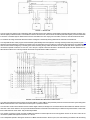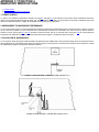
1
Sinclair QL Service Manual
Prepared by THORN (EMI) DATATECH LTD for SINCLAIR RESEARCH LTD
OCTOBER 1985
© Sinclair Research Ltd.
SERVICE MANUAL X-1204
List of Contents
SECTION 1 SYSTEM DESCRIPTION
SECTION 2 DISASSEMBLY/ASSEMBLY
SECTION 3 SYSTEM TEST
SECTION 4 FAULT DIAGNOSIS AND REPAIR
Appendix A Known Bugs and their Remedies
Appendix B User Hints
Appendix C Mandatory Modifications
Appendix D Microdrive Fault Finding
SECTION 5 PARTS LISTS
List of Illustrations
RS 232 Link
Keyboard Matrix Interconnections
QL Block Diagram
QL Circuit Diagram (Issue 5)
QL Circuit Diagram (Issue 6)
Motor Location Jig
Keyboard Format
Head Chassis
Issue 5 Board - Component Side Modification
Issue 5 Board - Solder Side Modification
Issue 6 Board - Solder Side Modification
Microdrive Signals (100 kHz WRITE)
Microdrive Signals (100 kHz READ)
Microdrive Signals (100 kHz FORMAT READ)
ULA 2G007 - Internal Circuit
Printed Circuit Board (Issue 5) Component Layout
Printed Circuit Board (Issue 6) Component Layout
History Sheet
MANUAL ISSUE TEXT CIRCUIT/LAYOUT DIAGRAMS
1
2
3
REMARKS
JANUARY 1985
JUNE 1985
Minor changes made to pages 1.5, 3.6, 4.1, 4.3, 4.4, 4.15, 4.17 and 5.7.
OCTOBER 1985
Appendices A, B, C and D added to Section 4.
SECTION 1
SYSTEM DESCRIPTION
LIST OF CONTENTS
1.
2.
3.
4.
5.
6.
7.
8.
9.
Introduction
Architecture
MC68008 CPU
Intel 8049 Intelligent Peripheral Controller (IPC)
Memory Organisation
Peripheral Control (ZX8301, ZX8302 and IC28)
Microdrive
Power Supplies
Test
RS232 Link
Keyboard Matrix Interconnections
QL Block Diagram
QL Circuit Diagram (Issue 5)
QL Circuit Diagram (Issue 6)
1. INTRODUCTION
1.1 The QL computer can be regarded in hardware terms as a combination of an enhanced Spectrum microcomputer, an Interface 1, an Interface 2
and two Microdrives within the same case. In practice the resemblance to the Spectrum is small, since the QL requires two microprocessors to
accommodate powerful new software and is provided with 128k bytes of inbuilt DRAM. A block diagram of the Sinclair QL is given in Figure 1.3.
1.2 Two main versions of the QL are in circulation. A certain number of boards to build standards up to Issue 5 were issued in either ROM or
EPROM versions with another ROM mounted pickaback in IC33 position. The second, volume production, version of the board to build standard
Issue 6, and subsequent, features 48k of on-board ROM realised in two memory devices. In the following description the two versions are referred
to as the pre-Issue 6 and the post-Issue 6 versions. The main differences between the two versions, as far as the circuit description is concerned,
are that IC17 and IC27 have been deleted and IC38 added in the post-Issue 6 version.
2. ARCHITECTURE
2.1 The architecture of the QL shown in Figure 1.3 incorporates much that is typical of microcomputer systems, but certain innovations make it
atypical. Two microprocessors, an Intel 8049 and a Motorola 68008 are used, and the availability of 128k of DRAM plus a minimum of 200k on the
two microdrives provides unusual storage facilities. The 8049 is designated the Intelligent Peripheral Controller (IPC) and the 68008 is the CPU.
Two additional semi-custom ICs ZX8301 and ZX8302 control defined areas of the system, under the supervision of the CPU.
2.2 The microcomputer electronics are housed on a single printed circuit board which also houses a regulated power supply fed from an external
power unit. The keyboard forms part of the upper case assembly and is connected to the p.c. board via J11 and J12. The microdrive headboards
and microdrive chassis, including the microdrives and the motors, form two complete sub-assemblies which plug in to the main p.c. board.
2.3 To the rear and side of the case are plug assemblies which accommodate the following:
1.
2.
3.
4.
5.
main expansion connector, J1
ROM cartridge, J2
joystick, J3, J4
RS232, J5, J6
extra microdrives, EC1
3. MC68008 CPU
3.1 The Motorola MC68008 is a 32-bit microprocessor with an 8-bit data bus and is responsible for the overall timing and control of the QL. The
firmware, which is outside the scope of this manual, resides in either a ROM or an EPROM depending on the version. The 68008 has an external
clock, generated by the ZX8301 and has the usual bus input/output arrangement, viz. data bus, address bus and control bus. It operates semisynchronously in this configuration.
3.2 Data Bus. D0-D7 forms an 8-bit bi-directional data bus with active high, tri-state outputs. It is used for data exchanges with the memory, with the
ZX8302 and ZX8301 and with the peripherals.
3.3 Address Bus. Twenty bits A0-A19 are available for select and address purposes. A0-A15 form a 16-bit address bus with active high. The
address bus provides the address for memory (up to 128k bytes) data exchanges and for data-exchanges with the QL and microdrive. Three bits
A0, A1 and A5 are used for this latter purpose. Bits A16-A19 are used for device selection.
3.4 Control Bus. The control bus is a collection of individual signals which supervise the flow of data on the address and data busses. The block
diagram shows most of these signals but reference to the circuit diagram shows other control signals available at the expansion port. Control lines
are summarised below.
3.5 Interrupt Control (IPL0/2, IPL1). These inputs indicate the encoded priority level of the device requesting an interrupt, and are fed by IC24 (pins
23, 24) and IC23 (pin 26). A satisfactory interrupt condition must exist for two successive clocks before triggering an internal interrupt request. An
interrupt acknowledge sequence is indicated by the function codes, FC0 and FC1. In this configuration FC0 and FC1 are NANDed together at
IC27,6 and the output routed to the valid peripheral address (VPA) input to the CPU. This input indicates that the processor should use automatic
vectoring for an interrupt. The IPL signals and VPA may also be input from an external device via J1, the main expansion connector.
3.6 A16 and A17. These two address bits select ZX8301 and are decoded by it to assert the relevant CAS0 and CAS1 signal and ROMOEH and
PCENL for the ZX8302 chip enable. For this purpose their states are either low and high, or high and low respectively. When ROM is being
addressed both are in the low state.
3.7 CLK Input. The CLK input denoted CLKCPU is the 7.5 MHz system clock from ZX8301. It is also fed to IC23 and IC24 and to the expansion
port connector.
3.8 Asynchronous data transfers are handled using the following control signals: DTACK, R/W, DS and AS. These signals are explained in the
following paragraphs.
3.9 DTACK (Data Transfer Acknowledge). This input indicates that the data transfer is completed, and is sent by the ZX8301 or through the
expansion connector. When the processor recognises DTACK during a read cycle, data is latched and the bus cycle is terminated. When DTACK
is recognised during a write cycle, the bus cycle is terminated.
3.10 R/W. This tri-state signal defines the data bus transfer as a read or write cycle. The R/W signal also works in conjunction with the data strobe
as explained in the following paragraph.
3.11 DS (Data Strobe). This tri-state signal controls the flow of data on the data bus as shown in the table below. When the R/W line is high, the
processor reads from the data bus as indicated. When the R/W line is low the processor writes to the data bus as shown.
DS R/W
1
0
0
D0-D7
No valid data
1 Valid Data Bits 0-7 (Read Cycle)
0 Valid Data Bits 0-7 (Write Cycle)
If the CPU is addressing an external device with one of address bits A18 and A19 set, emitter follower TR8 is switched on by the signal KILLH from
IC38. This sets the DSMCL (Data Strobe Master Chip - Active Low; the 'Master Chip' is the ZX8301) line permanently high thus disabling IC23 and
IC22. The local DS signal is still enabled to J1, the expansion port, to control R/W operations from an external device. In the pre-Issue 6 version
TR8 is switched from IC18.
3.12 AS (Address Strobe). This tri-state signal indicates that there is a valid address on the address bus.
3.13 Four other groups of control signals are used by the CPU. These four groups are routed to J1 only and are associated with Bus Arbitration
Control, Peripheral Control, Processor Status and System Control in respect of external devices.
3.14 Bus Arbitration Control. An explanation of this function is included for information only. It is not used by the QL but could be used by
peripherals. The 68008 contains a simple 2-wire arbitration circuit designed to work with daisy-chained networks, priority encoded networks, or a
combination of these techniques. This circuit is used in determining which device will be the bus master device. The BR (Bus Request) input is wire
ORed with all other devices that could be bus masters. This device indicates to the processor that some other device desires to become the bus
master. Bus requests may be used at any time in a cycle or even if no cycle is being performed. The BG (Bus Grant) output signal indicates to all
other potential bus master devices that the processor will release bus control at the end of the current bus cycle.
3.15 M6800-compatible Peripheral Control is exercised through the VPA and E output lines. VPA is derived from two processor status signals
FC1 and FC0 as described above though this is only used for auto vectoring. E (Enable) is the standard enable signal common to all M6800 type
peripheral devices. The period for this output is 10 MC68008 clock periods (six clocks low, four clocks high).
3.16 Processor Status (FC0, FC1 and FC2) are function code outputs which indicate the state (user or supervisor) and the cycle type currently
being executed, as shown in the table below. The information indicated by the function code outputs is valid whenever address strobe (AS) is
active.
Function Code Output
FC2 FC1 FC0
LOW
LOW
LOW
LOW
HIGH
HIGH
HIGH
LOW
LOW
HIGH
HIGH
LOW
LOW
HIGH
Cycle Type
LOW (Undefined, Reserved)
HIGH
User Data
LOW
User Program
HIGH (Undefined, Reserved)
LOW (Undefined, Reserved)
HIGH
Supervisor Data
LOW Supervisor Program
HIGH
HIGH
HIGH Interrupt Acknowledge
3.17 System Control inputs are used to either reset or halt the processor and to indicate to the processor that bus errors have occurred. There are
three system control signals: BERR, HALT and RESET.
3.18 BERR (Bus Error). Not used on the QL.
3.19 RESET and HALT. The bidirectional RESET signal line acts to reset (start a system initialisation sequence) the processor in response to an
external RESET signal. An internally generated reset (result of a reset instruction) causes all external devices to be reset and the internal state of
the processor is not affected. A total system reset (processor and external devices) is the result of external HALT and RESET signals applied at
the same time. HALT and RESET are tied together on the QL.
4. INTEL 8049 INTELLIGENT PERIPHERAL CONTROLLER (IPC)
4.1 The 8049, IC24, is a totally self-sufficient 8-bit single chip microcomputer containing 2 k bytes of program memory and 128 bytes of RAM. It is
clocked internally at 11 MHz from crystal X4.
4.2 In this application the function of the 8049 is to:
1.
2.
3.
4.
receive RS232 interface signals,
monitor the keyboard,
control the loudspeaker,
control the joystick.
The IPC utilises a data bus, two 8-bit I/O ports and some control lines to control these functions.
4.3 Data Bus. DB0-DB7 constitutes an 8-bit bi-directional data bus with active high tri-state input/outputs. It is used only as input for scanning the
keyboard and joysticks.
4.4 Control Bus. Control is exercised by a number of discrete signals which organise the direction and flow of data between the 8049 and the
ZX8302, and also communicate with, and monitor, other areas of the QL.
4.5 Control Lines. The role of each control line is as follows:
1.
2.
3.
4.
5.
6.
7.
8.
9.
10.
11.
T1. Timer/Counter Input, 4 times the baud rate set by the user, controlled by a ZX8302 register.
WR. Output strobe, active low, used as a read or write strobe to enable keyboard, joystick or RS232 data to IC23 over the P27 link line.
P10-P17. Output lines used to scan the keyboard and joysticks in conjunction with DB0-DB7.
P26. Not used on QL.
P21. Loudspeaker output.
P27. Serial link transmitting data to IC23.
P24, P25. RS232 handshake lines.
RESET. Input from IC23 used to initialise the 8049.
CLKCPU. Clock input from ZX8301.
P23, P22 (IPL1, IPL2). Interrupt request lines to 68008 CPU.
INT, P20. Interrupt input. INT initiates an interrupt on reception of RS232 first transition. P20 is used to read the data on the RS232 receive
lines.
4.6 RS232 Link. IC24 is responsible for the receive side of the RS232 serial data link only, and IC23 the transmit side. Since, the RS232 link is
best understood as an entity both aspects are discussed here.
4.7 J5 and J6 are two RS232 connectors. J6 is connected so that the device connected to it may act as the Data Terminal Equipment (DTE) which
originates the Data Terminal Ready (DTR) signal. J5 connects to the Data Communications Equipment (DCE) i.e. the local QL assumes DTE
status. Figure 1.1 illustrates this schematically.
4.8 The RS232 interface uses an 11-bit ASCII data frame, viz. one start bit, eight data bits and two stop bits comprise one character. Two stop bits
are always sent but the interface receives compatibly with one except at 9600 baud, where one and a half stop bits are required. Data is
transmitted asynchronously in the full duplex mode.
4.9 Consider the QL as the DTE. Both DTE and DCE are switched on and have their DTR signals asserted. CTS and DTR (Clear to Send, Data
Terminal Ready) do not form a handshake pair but are similar signals going in opposite directions. Serial data is transmitted by IC23 via driver
IC25/6 and received by line receiver IC26/11. From IC26/11 data is fed to NAND gate IC27/9, pin 10 of which is set to the high state by the
program, and input to IC24 pins 6 and 21 via IC27/11.
FIGURE 1.1 RS232 LINK
4.10 On receipt of a start bit, IC24 is interrupted, and a subroutine clocks in the data bits, synchronised by the baud rate generator. The data, up to
about 20 bytes per RS232 channel, is tnen buffered in IC24. At the same time, IC24 receives commands (and sends reports) via the serial link with
IC18 which i-s controlled by IC23. When IC24 receives a command from IC18 to empty one of its buffers, it does so, down the serial link via IC23.
4.11 With the QL acting as the DCE data and control is managed in a similar way utilising different IC25 and IC26 receivers/drivers.
4.12 Keyboard Monitor. Under program control the 8049 systematically scans the keyboard, recording which keys have been pressed. Figure 1.2
shows the way the keyboard is connected. It consists of an 8 x 8 matrix with one key, the shift key, connected to three input lines. The intersection of
each row and column is bridged by a normally open contact. Pressing the key closes this switch. The row 'outputs' and column 'inputs' are shown
connected to separate connectors J11 and J12, one to the port 1 outputs of IC24 and the other to the data bus inputs. Pull-down resistors R17 to
R24 ensure that when none of the key-switches are closed row inputs KBO0 to KBO7 remain low.
FIGURE 1.2 KEYBOARD MATRIX INTERCONNECTIONS
4.13 When the keyboard scanning routines are entered (KBOn is output, KBIn is input) the 8049 performs successive I/O read cycles setting each
KBO0 to KBO7 line low in turn. At the same time the I/O port 1 inputs are scanned.
4.14 There are a total of eleven diodes used for isolation. Eight of these, D4 through D11 are isolation diodes which isolate the different rows from
each other. Three of the diodes D1 to D3 provide individual isolation for the Shift Control and Alt keys so that these keys have diodes in series with
them in both directions of the matrix. They are thus fully isolated.
4.15 Joystick. Connectors J3 and J4 provide a FIRE input and the four switch inputs for each of two joysticks. One line is not used. J3 and J4 are
connected in parallel with keyboard connectors J11 and J12.
4.16 Loudspeaker Operation. During the execution of a BEEP instruction the IPC writes to port 2, P21 thus switching on transistor TR1 and driving
the loudspeaker. The loudspeaker is damped by resistor R104 (post-Issue 6 only).
5. MEMORY ORGANISATION
5.1 Introduction
5.1.1 The pre-Issue 6 version was supplied in both EPROM and ROM forms with on-board straps enabling the selection of ROM. Both versions
have 48k of ROM and in both versions there are 128k bytes of RAM memory. Figure 1.3 shows how the memory is organised.
5.1.2 The lower 48k bytes (addresses 0000-BFFF) are implemented in one 32k and one 16k byte ROM, IC33 and IC34 respectively which hold the
monitor program. This program is a complex 68008 machine code program divided broadly into two parts: the operating system and the BASIC
interpreter. Details of the program content are outside the scope of this manual.
5.1.3 32k bytes of memory (addresses C000-FFFF) have been left assigned to the ROM cartridge while 128k bytes of RAM (addresses 200003FFFF) are implemented on sixteen 64k-bit dynamic RAMs, IC1-IC16.
5.2 Read/Write Operations
The following description should be read in conjunction with the circuit diagrams given in Figures 1.4 (pre-Issue 6) and 1.5 (post-Issue 6).
5.2.1 Read Only Memory. The CPU addresses the ROM/EPROM directly during memory read cycles using the address bus A15-A0. In the preIssue 6 version, depending on the ROM/EPROM fit, the enabling and selection pins on IC33 and IC34 are set by link selection on IC17. Links JU1
to JU6 via gate circuit IC17 are used to provide the correct signals; the link fit requirements for different ROM/EPROM versions is listed on the
circuit diagram, Figure 1.4. In the post-Issue 6 version the ROMs are enabled directly by the signal ROMOEH from ZX8301.
5.2.2 RAM Memory (IC1-IC16). The sixteen RAM ICs making up the 16k x 64 bit RAM memory are organised as two matrices of 256 rows x 256
columns i.e. IC1-8 and IC9-16. Thus, separate 8-bit row and column addresses are required to access any one of the 64k locations in each
section. These addresses are supplied by the CPU (68008) on address bus A0 to A15 via tri-state address multiplexers IC19 and IC20. These
multiplexers decode from sixteen to eight lines and outputs enabled by the row address select line (RASL) signal from the ZX8301. The valid data
address (VDA) selects the address from the CPU (via multiplexers IC19, IC20) or from the ZX8301. ROWL from the ZX8301 selects the
row/column address. The R/W signal from the CPU informs the ZX8301 to expect either a read or a write cycle. For a write cycle the ZX8301
enables the write enable (WEL) line to the memory.
5.2.3 The eight bits each of column and row address are routed to both 64k sections of the RAM but the signals 'column address select 0' (CAS0L)
and 'column address select 1' (CAS1L) from the ZX8301 ensure that only the required half of the memory is active. Address bits A16 and A17 from
the CPU are decoded by the ZX8301 to enable the relevant CAS signal. The row address select line (RASL) signal from the ZX8301 is enabled
during all read and write cycles from RAM.
5.2.4 The ZX8301 has priority when accessing memory since it must access the memory mapped display area in the RAM at set intervals in order
to build up the video for the TV display. When the ZX8301 requires to access memory, it asserts the VDA signal to CPU address multiplexers
IC19, IC20 and addresses RAM directly via its own address bus on pins 13, 17, 18, 20, 22, 24, 27 and 28.
5.2.5 Isolation between the two data busses D0-D7 and DB0-DB7 is accomplished using bus transceiver IC21. During ZX8301 memory cycles
IC21 is disabled by negating the signal DEL from Hard Array Logic (HAL) IC38. This signal is controlled by ZX8301 signal TXOEL. In the pre-Issue
6 version, which does not incorporate the HAL, TXOEL is fed directly to IC21.
5.2.6 Refresh for the DRAM memory is accomplished during normal read cycles i.e. most rows are refreshed each time the ZX8301 accesses the
memory mapped display area during picture compilation, the remaining rows are refreshed as a result of other read cycles also known to occur at
regular intervals within the refresh period.
6. PERIPHERAL CONTROL (ZX8301, ZX8302, IC38 and IC28)
6.1 ZX8301, IC22.
The ZX8301 carries out the following functions:
1.
2.
3.
4.
5.
TV picture generation
master clock generation
system address decode
DRAM refresh
control of the bus transceiver.
6.1.1 The TV picture generation section of IC22 operates in conjunction with the memory mapped picture display area to produce five colour TV
signals suitable for driving a colour monitor. These signals, red, green and blue (RGB), CSYNCL (composite sync) and VSYNCH (vertical sync) are
routed to connector J7. The RGB and CSYNCL signals are also input to IC28 which produces composite PAL to drive a domestic TV receiver. The
same signals are mixed in transistor TR9 to produce a composite video signal to drive a standard monochrome monitor. VSYNCH is also routed to
IC23 where it is used to provide an interrupt at the frame rate. This is used to give a time reference to the job scheduling supervisor in the operating
system.
6.1.2 Using the 15 MHz crystal clock, X1, IC22 derives line and field timing compatible with the external receiver. Video is derived by accessing the
memory mapped display area in the RAM in a set sequence at set times throughout the picture frame. The addresses are necessarily independent
of the CPU and appear on IC22 address lines DA0 through DA7.
6.1.3 The net result is the five video signals output from IC22 on pins 32, 31, 30, 12 and 11.
6.1.4 The RGB signals are fed to level-setting resistor divider network R48-R53 and a.c. coupled to RGB-to-PAL converter IC28 on pins 3, 4 and 5.
The composite sync signal CSYNC is input on pin 2. External components of the circuit provide a number of clamp circuits; the luminance and
chrominance signals are fed out, filtered and fed back in; the chrominance 4.43 crystal oscillator is connected; and a CR lead/lag network
introduces a 90° phase shift. The crystal has a very high tolerance and does not need trimming.
6.1.5 The composite PAL signal is output on pin 9, divided down and applied to an encapsulated UHF modulator M1.
6.1.6 Master clock is divided by two in IC22 from the externally connected 15 MHz crystal X1 and distributed via output pin 7 to various destinations
on the board, and to J1 the main expansion connector.
6.1.7 The system address decode signal PCENL, routed to peripheral controller ZX8302 pin 10, is derived differently on the two board versions.
On the pre-Issue 6 board it is output from ZX8301 pin 39 and is derived from a combination of one of the decodes from address lines A16 and
A17, and A14 (via DA6). In the post-Issue 6 version it is output from HAL pin 17 and is derived in a similar way from a decode of address lines
A16, A17 and A6.
6.2 ZX8302, IC23.
The ZX8302 is termed the peripheral chip since it controls all signals to and from the peripheral devices. Signals to/from the following are
supervised:
Keyboard
Speaker
by serial link to IPC
Joystick
RS232 (half)
RS232 (half)
Net
Microdrive
Real-Time clock
Interrupt control
6.2.1 IC23, in common with IC24, works autonomously and is polled by the CPU. It has its own 32 kHz crystal clock X2 and has an external interrupt
input on pin 2 from J1, the expansion connector. Switch S3 connected to pin 21 resets the device when operated. Pin 28 output resets the CPU
and IPC.
6.2.2 Address lines A0, A1 and A5 from the CPU select the specific device requiring service viz: one of (a) to (e) in paragraph 5.2 above. The
VSYNCH and PCENL signals input on pins 10 and 32 have been discussed in paragraph 6.1.1 and 6.1.7 respectively. The DSMCL signal is
discussed in paragraph 3.11.
6.2.3 Serial data from the various devices is converted to parallel data in IC23 and output to the data bus as DB0-DB7. Parallel data from the bus
is converted to serial data and routed to the relevant device for transmission.
6.2.4 The RS232 serial link, the keyboard and the joystick operation have already been discussed in the 8049µC (IC24) section.
6.2.5 The two Net jack plugs J9 and J10 are connected in the same way as in the Spectrum Interface 1 circuit. The network is common emitter in
that all stations on the network can either source current into the net or be turned off, i.e. be set in tri-state. Jack plugs are used such that those
sockets which are unused serve to terminate the network.
6.2.6 When a jack is inserted in the socket it opens up a connection to a 330Ω resistor, R15 or R16, disconnecting it from the circuit. With a
network set up, the two end stations would be the only ones with the 330Ω resistors in circuit. There is therefore their combined resistance, giving a
pull-down impedance of about 165Ω to the circuit. IC23 contains the interface and control circuitry for the network.
6.2.7 The real-time clock is run from the 32 kHz crystal X2 on pins 31 and 30. Date and time are resettable under software control. On pre-Issue 6
QLs, a trimming capacitor TC1 enabled trimming of the oscillator frequency. On the post-Issue 6 the trimming capacitor has been replaced by a
fixed capacitor.
6.2.8 The remaining lines out from IC23 are the microdrive control and data lines on pins 3, 1, 19, 21, 33 and 34. These inputs and outputs are
discussed in Section 7, MICRODRIVE.
7. MICRODRIVE
7.1 Introduction
7.1.1 Microdrive organisation and control in the QL is similar to that found in the Spectrum, bearing in mind that the two QL microdrives are
integrated into the system and that Interface 1 functions are all executed by IC23; also the frequency is different and write protect is different.
7.1.2 Additional microdrives may be connected to the system via connector EC1.
7.1.3 Only one microdrive may be in use at any instant. The required microdrive and the type of operation, read or write, is selected under software
control. During a read operation data is read from the selected microdrive tape. During a write operation the microdrive tape is erased before
being written. The erase head is displaced from the write head and is timed by IC23 to sink current before the write head is enabled.
7.2 Microdrive Selection
7.2.1 Microdrives are selected using the MDSELDH and MDSELCKN signals from IC23. Each microdrive control chip, IC29 and IC30, contain one
stage of a shift register, realised by a flip-flop. MDSELCKN is connected to each microdrive and MDSELDH is routed to pin 22 (COMMS IN) of
IC29, which is the input to the shift register. The shift register output on pin 20 (COMMS OUT) is routed to COMMS IN in IC30. COMMS OUT on
IC30 pin 20 is routed to microdrive expansion connector EC1. The selected microdrive has a '1' on its COMMS OUT pin. Thus the required
microdrive is selected by shifting the '1' accordingly.
7.2.2 COMMS OUT not only feeds the next microdrive; it is used to select its own chip internal functions and to select the LED, the motor, and the
erase current for the selected microdrive. Therefore while this signal is low the motor is disabled, the LED is off, no current can flow through the
microdrive switch (S1 or S2), and no erase current can flow.
7.2.3 Consider the motor drive circuit for number 1 motor. A high on pin 20 of IC29 turns on TR4. This pulls the base of TR6 low, turning it on and
switching power to motor 1. Capacitor C21 and resistor R28 time constant ensures that the motor does not cut out too quickly and damage the
tape. The red LED D20 is switched on at the same time. With TR6 turned on and write protect switch S1 closed the erase head current circuit is
enabled via pin 6 of headboard 1 connector. When the erase output is enabled on pin 1 of IC23, transistor TR3 switches on and current flows in the
selected microdrive erase head. Diodes D18 and D16 provide protection against reverse currents. Diodes D12 across the erase head and D15
perform similar functions. The amount of current flowing in the erase head is limited by R25.
7.2.4 Write protection is achieved by the action of the microswitch on the microdrive chassis. The switch is operated by the write protect tab on the
microdrive cartridge. When the tab is present the select supply line is connected to the erase coil, enabling the QL to write normally. When the tab
is absent, the supply to the erase head is disconnected, and the MDRDWL line is held high (read mode) via R100/101 and D22/23 (see Section 5,
para 3.1). This line is clamped to 5 volts maximum by diode D29. The purpose of D22/23 is to prevent unselected microdrives with no cartridge
inserted (or with writeprotected cartridge inserted) from loading the MDRDWL line.
7.3 Read/Write Operations
7.3.1 The MDRDWL signal on IC23 pin 3 places the selected microdrive in either the read or the write mode, and enables the read or the write
amplifiers.
7.3.2 Data is recorded on two tracks using a standard stereo cassette head arrangement and is written in bytes, one byte to one track and the next
byte to the other track. It is recovered in the same way. The tape itself is one continuous loop. Since hardware takes care of switching between
tracks the software sees the tape as one doublelength single track.
7.3.3 Power to the microdrive circuits has to be filtered and IC31 and capacitors C9 and C11 are used to accomplish this. IC31 is the regulator.
7.3.4 Read Cycle. Consider IC29 and headboard 1. In the read mode the signals appearing in the two read coils inside the heads are differentially
amplified through two amplifier chains within IC29. The signals are then converted to digital form to enable logic processing. The outputs from the
two amplifiers, in digital form are enabled into the DATA 1 and DATA 2 outputs from IC29 on pins 24 and 19. These signals are routed to the
interface within IC23 via RAH (Read and Write) 1 and 2, pins 21 and 19.
7.3.5 The signal recorded on magnetic tape is at the greatest when the rate of change of the signal imposing it is at its fastest. Therefore when a
squarewave has been written, the greatest recovered voltage is obtained on the edge of the pulse. Since the object of the exercise is to produce a
waveform which changes at the peaks of the recovered signal, IC29 contains amplifiers to bring the signal up to the required level, and a peak
detect circuit which changes state when the input reaches its greatest level. The peak detector is followed by a hysteresis circuit which ensures that
the output does not change on spurious signals.
7.3.6 The gain of the circuit should not need to be changed, as only one type of high quality video tape is used. The reproduced signal levels may
be read across capacitors C15 and C17 and are typically in the order of 400 to 500 mV and 250 to 350 mV for the low frequency and high
frequency signals respectively. In the record mode the modulator in IC23 converts the ones and zeros in the data into FM (frequency modulation)
where there is always a transition at the beginning of the bit cell. If the data is a one there is a transition at the beginning and in the middle of the bit
cell, which means essentially that the frequency doubles if the data contains ones. Hence high and low frequencies at C15 and C17.
7.3.7 Write Cycle. When the MDRDWL signal from IC23 goes low the selected microdrive is placed in the write mode. This has the effect of
changing DATA 1 and DATA 2 on IC29 from outputs to inputs. These inputs are used to drive current sources for track 1 and track 2. When DATA
1 is high for example, current is pulled in one direction through the head, when it is low current is pulled in the other direction.
8. POWER SUPPLIES
8.1 A custom-built power pack, external to the main board, supplies 9 volts d.c. at 2 amps and 44 volts peak-to-peak a.c. to the board input on
connector J3. The power pack uses a thyristor to limit peak voltages on the d.c., but is otherwise unregulated and has significant ripple.
8.2 The a.c. input is applied to two rectifiers IC37 and IC36 to produce +12 volts at 80 milliamps and -12 volts at 50 milliamps, respectively.
8.3 The d.c. input is regulated down to +5 volts by regulator IC35.
8.4 All three supplies are completely protected in that the regulators are equipped with thermal and short circuit shutdown.
9. TEST
9.1 A good simple test of the equipment may be carried out by connecting a loopback cable to the RS232 interface connectors J5 and J6 and
instructing them to talk to each other. The technique for receiving RS232 involves the data passing through the IPC, through ZX8302 and back onto
the processor data bus. If this functions correctly it is close to a guarantee that the whole system is functional.
9.2 A test tape is available which exercises most of the functions of the QL and is a useful initial diagnostic tool. See Section 3 for details.
FIGURE 1.3 QL BLOCK DIAGRAM
FIGURE 1.4 QL CIRCUIT DIAGRAM (Issue 5)
FIGURE 1.5 QL CIRCUIT DIAGRAM (Issue 6)
SECTION 2
DISASSEMBLY/ASSEMBLY
1. Disassembly
Access to Internal Components
Microdrive
Circuit Board
Loudspeaker
Microdrive: Disassembly for Repair
Keyboard: Disassembly for Repair
2. Assembly
Loudspeaker
Circuit Board
Microdrives
Keyboard
Case Assembly
1. DISASSEMBLY
1.1 Access to Internal Components
1.1.1 Unplug all input/output leads and turn the QL upside down to reveal eight self-tapping screws, 4 x 5/16-in along the front edge, below the overhang, and 4 x 1.1/4-in along the rear edge. Remove the screws (CAUTION: do not remove the two screws visible on the base immediately below
the microdrives). Hold the two halves of the case together and return the QL right-side up. The top half of the case, including the keyboard, can now
be separated from the bottom half, although it remains connected to it by two flexible ribbon cables and the leads from three LEDs.
1.1.2 To separate the upper and lower case halves completely, free the membrane tails from the edge connector sockets on the board by pinching
them between forefinger and thumb (adjacent to the socket) and then exerting upward pressure. Release six leads from the 'snapaction' wire post
socket, adjacent to the TV modulator can, by pinching the black plastic moulding between forefinger and thumb and raising it up off the board until
resistance is felt; the leads can then be pulled free.
1.2 Microdrive
1.2.1 Remove the heatsink adjacent to the microdrives by releasing the attachment screw for the +5V regulator IC35; retain the M3 x 10mm screw
with brass plain and crinkle washers for assembly.
1.2.2 Remove three pan-head, self-tapping screws securing the microdrive to the lower case - two visible at opposite corners of the microdrive
chassis (5/16-in and 1/2-in). CAUTION: not to be confused with the countersunk motor screws and a third (3/4-in) accessible from the underside of
the lower case.
1.2.3 Lift the microdrive from its mounting position and free the two ribbon cables from sockets on the board by pinching them between forefinger
and thumb (adjacent to socket) and then exerting upward pressure.
1.3 Circuit Board
1.3.1 Remove both microdrives as detailed in para 1.2. Remove the reset button.
1.3.2 Release the loudspeaker leads from the 'snap-action' wire post socket, adjacent to the TV modulator can, together with two pan-head screws
securing the circuit board to the lower case. The screws are located in the vicinity of the external bus connector and the loudspeaker; retain the 1/4in screws and fibre washers for assembly.
1.3.3 Remove the push-fit microdrive extension bung from the lower case, and carefully work the circuit board free from the locating dowels by lifting
it at the bus extension connector end.
1.4 Loudspeaker
1.4.1 Remove the microdrives and circuit board as detailed in paras 1.2 and 1.3.
1.4.2 Using a scalpel or similar tool, break the adhesive seal between the loudspeaker housing and the lower cover and lift the speaker from the
locating dowels.
1.5 Microdrive: Disassembly for Repair
1.5.1 Stripping for repair is limited to the p.c. board, motor assembly and the microswitch. Each is secured by screws, readily identified once the
microdrive is removed from the lower case.
1.6 Keyboard: Disassembly for Repair
1.6.1 Separate the upper and lower case halves as described in para 1.1.
1.6.2 Release six 1/4-in pan head screws securing the keyboard backing plate to the upper case. This allows the plate, with membrane attached,
to be lifted clear revealing the keyboard bubble mat below. The membrane is separated from the plate by carefully breaking the adhesive seal
holding the ribbon cables in position; the bubble mat is simply lifted from its position revealing a set of keys below.
1.6.3 Individual keys can be removed for cleaning by holding the key depressed and gently prising the retaining sleeve off the underside of the key
using a small screwdriver inserted under the rim.
2. ASSEMBLY
2.1 Assembly of the QL and its component parts is generally the reverse of disassembly. Points worthy of note are given below.
2.2 Loudspeaker. Attach double-sided adhesive tape, locate base over locating dowels adjacent to grille in the lower case and apply pressure to
effect an even bond.
2.3 Circuit Board. Locate RESET button end first and once secured, replace the microdrive extension bung and loudspeaker leads. Replace reset
button.
2.4 Microdrives. The ULA on the microdrive fitted in the left-hand (MDV1) position is protected by an RF shield. Ensure that the shield is in place
before starting re-assembly. Start assembly by straightening the bare wire-ends of the ribbon cables and then pushing them hone in their
respective sockets. Care is required to ensure the connections are made satisfactorily.
2.5 Keyboard. The bubble mat, membrane and backing plate are perforated to accommodate six locating dowels moulded in the upper case. It
may prove advantageous to release the adhesive bond between the membrane and the backing plate to aid alignment.
2.6 Case Assembly. Before screwing the case halves together, reconnect the keyboard ribbon cables and LEDs to their sockets on the circuit
board. The LED connections are as follows:
Pin Diode Wire Colour
1
2
3
4
5
6
D21k
D21a
D20k
D20a
D27k
D27a
Black
Grey
Black
White
Black
Red
Function
MDV2 (red)
MDV1 (red)
POWER (yellow)
SECTION 3
SYSTEM TEST
1. Introduction
2. System Test
3. Procedure
1. Power-Up
2. Colour Test
3. Sound Test
4. Network Test
5. RS232C Loopback Test
6. Keyboard Test
7. Joystick Test
8. Real-Time Clock Test
9. Microdrive 2 Test
10. Microdrive 1 Test
11. Microdrive Tape Not Inserted Correctly
12. End of Test
1. INTRODUCTION
1.1 The use of the following test procedure is strongly recommended after carrying out unit repairs, thus ensuring that a once defective unit is
completely operational before return to the owner. The procedures can also be used effectively during fault diagnosis (Section 4).
1.2 Adjustments. The pre-Issue 6 QLs have a trimming capacitor TCI associated with the real time clock. It is factory-set to give a clock frequency
of 32.768 kHz at IC23 pins 30 and 31 and should not require further adjustment.
2. SYSTEM TEST
2.1 The system test is conducted with the QL connected to a colour monitor and a domestic colour TV receiver so checking both display paths.
Additional test equipment is required as follows:
1.
2.
3.
4.
System 2 Test Software - supplied as microdrive cartridge.
2-off blank microdrive cartridges - passed as being suitable for system test.
RS232C loopback cable
2-off industry standard joysticks
2.2 With the QL powered-up and the test software loaded and running, the test progresses through 9 well-defined states during which each of the
QL's functions is exercised. Some stages require the operator to respond to prompts displayed on the TV/monitor, others run autonomously
outputting only a test 'passed' or 'failed' message. At the end of system test the message QL TEST COMPLETE is displayed.
3. PROCEDURE
3.1 Power Up
3.1.1 Connect the QL and power-up as if for normal use; check that the yellow 'power on' LED is illuminated and the following message is
displayed on both screens:
3.1.2 Connect the RS232 loopback cable, connect the joysticks to the QL's CTL1 and CTL2 sockets, insert the system 2 test cartridge in
microdrive 1 (MDV1) and press the F2 key. Check that the microdrive 1 LED lights up when the drive is running.
3.1.3 At some stage during program loading a title page is displayed briefly. A short time later two bleeps are heard and a message is displayed
requesting a blank cartridge to be placed in MDV2.
3.1.4 Insert a blank tape cartridge into MDV2 as requested.
3.2 Colour Test
3.2.1 After the message to load a blank cartridge into MDV2 is displayed, both screens should clear and then display the following colour test card.
NOTE: On each colour bar the word 'Test' should be written 8 times, once in each of the following colours from top to bottom Black - Blue - Red
- Magenta - Green - Cyan - Yellow - White
3.2.2 Check that the colours on the monitor are the same as those on the TV; check that the flashing text is satisfactory; type OK to proceed.
3.3 Sound Test
3.3.1 Check that the following is displayed:
3.3.2 After hearing two cycles of trimphone followed by the low pitch tone, type OK to continue.
3.4 Network Test
3.4.1 Check that the following is momentarily displayed:
Network test : OK
3.5 RS232C Loopback Test
3.5.1 Check that the following is displayed:
3.5.2 Connect the loopback cable in the QL's SER1 and SER2 sockets and press the space bar; the following message should be temporarily
displayed:
3.6 Keyboard Test
3.6.1 Check that the following is displayed:
3.6.2 Press the key indicated by a dark blue background on the display. The blue background should be replaced by green and move onto the next
key. Press all keys in sequence and note that on pressing the ALT key the message: 'keyboard test complete' is displayed momentarily.
NOTE: Each key should be pressed individually, NOT skimmed over. If keys have a tendency to stick, the cause should be investigated.
3.7 Joystick Test
3.7.1 Check that the following is displayed:
3.7.2 Ignore the message concerning the joystick test board (intended for factory use only). Instead press the F1, F2, F3, F4 and F5 keys on the
keyboard followed by the Left, Right, Space, Up and Down keys on the keyboard. The background colour of each key on the display should change
from blue to green as in the keyboard test. On pressing the last key the message 'joystick test complete' is displayed momentarily.
3.8 Real-Time Clock Test
3.8.1 Check that the following are displayed momentarily:
3.9 Microdrive 2 Test
3.9.1 Check that the following message is displayed and that MDV2 starts to run and the corresponding red LED is illuminated.
3.9.2 Insert a blank cartridge in MDV1.
3.9.3 After a short delay the following message should be displayed:
NOTE: On pressing the space bar two bleeps should be heard and the following message displayed in green:
Microdrive 2 test OK
3.10 Microdrive 1 Test
3.10.1 As microdrive 2 test (para 3.9).
3.11 Microdrive Test Not Inserted Correctly
3.11.1 If during either microdrive test, the cartridge is not inserted correctly the following message is displayed in red:
3.11.2 Re-insert the cartridge in MDV1 or MDV2 as appropriate and press the space bar. If the test fails a second time the following message is
displayed:
3.11.3 Insert a new cartridge in MDV1 or MDV2 as appropriate and press the space bar. If the test fails again the message in para 3.11.1 is
repeated; re-insert the cartridge and press the space bar.
3.11.4 If the test fails a fourth time, the following message is displayed and the test is abandoned.
3.12 End of Test
3.12.1 On satisfactory completion of Microdrive 1 Test the following message should be displayed on green:
QL TEST COMPLETE
3.12.2 Press the RESET pushbutton and check that the display is as shown in para 3.1.1.
SECTION 4
FAULT DIAGNOSIS AND REPAIR
1. Introduction
1. Test Equipment
2. Modification History
3. Mandatory Modifications
2. Fault Diagnosis
1. Techniques
2. Power Up
3. Keyboard
4. Microdrive
5. Video
6. Fault-Finding Guide
3. Repair
4. Firmware Upgrade
1. INTRODUCTION
1.1 Test Equipment
1.1.1 Section 4 is intended as a guide to fault diagnosis and repair. It is assumed that users have a reasonable knowledge of electronic servicing,
theory and standard fault-finding techniques and have access to the test equipment and tools required to carry out the task. The table below
contains a list of the minimum test equipment and materials.
EQUIPMENT
SPECIFICATION/MANUFACTURER
Oscilloscope with probe (x1O)
Multimeter
Colour Television
New microdrive cartridges
Head cleaner
Double-sided adhesive tape
Extension ribbon/connectors for J11, J12 and front panel LED wiring (to enable operation with cover off)
ZX Microdrive
Motor location jig
Rise time: 0.02 µs/cm
General purpose
Open market
as required, Sinclair
Open market
Open market
Make up on site
Sinclair
See Figure 4.1
1.1.2 See Section 5 for the board layouts of the Issue 5 and Issue 6 boards.
FIGURE 4.1 MOTOR LOCATION JIG
1.2 Modification History
1.2.1 The only area that has seen substantive modification is the ROM/EPROM section of the memory. The following table sets out the various fits.
Build Standard IC
ROM/EPROM
Software Standard
Remarks
Build Standard IC
D6
D7
D8
D9
D10
D11-D14
IC33
IC34
IC33
IC34
IC33
IC34
IC33
IC34
IC33
IC34
IC33
IC34
ROM EPROM
32k
32k
16k
32k
16k
Software Standard
Remarks
AH
16k of EPROM mounted pickaback on IC33
JM
16k of EPROM mounted pickaback on IC33
32k
16k
32k
16k
15k
32k
16k
-
AH
AH
JM
JM
1.2.2 A newly laid out p.c. board was introduced at Issue 6 to reflect the removal of IC17 and IC27 and the addition of HAL IC38. Resistors R102,
R103 and R104 were added at this stage and trimming capacitor TC1 was replaced with a fixed capacitor C53 of 22pF. The parts list reflects
minor changes to component values. Board layouts are shown in Figures 5.1 and 5.2.
1.3 Mandatory Modifications
Certain component modifications have been introduced to improve performance in specific areas. These components should be checked for on all
units coming in for repair, and if necessary, fitted as a matter of course. These components are listed below:
1. Add resistor R104 (82 Ω) in TR1 collector circuit. It should be noted that this resistor is fitted in a non-standard way in the collector leg
between the transistor and the board.
2. Replace resistor R92 (was 220 Ω) with a resistor of value 390 Ω.
3. Add resistor R105 (1 KΩ) across capacitor C19.
4. Add resistor R106 (1 KΩ) across diode D17.
5. Add diode D22 (1N4148) in series with R100.
6. Add diode D23 (1N4148) in series with R101.
7. Add resistors R102, R103 (33 KΩ) between pins 19 and 21 of IC23 and VM12 (-12V rail). It is convenient to do this by laying the resistors on
top of IC23 and running a flying lead from their common connection to pin 1 (VM12) of IC25.
8. If EPROMs are fitted, upgrade firmware (IC33, IC34) to D11 standard and return salvaged EPROMs to Sinclair Research Limited. Details of
the methods used to upgrade to D11 standard are set out in sub-section 4.
9. Add MDV2 stand-off spacer.
2. FAULT DIAGNOSIS
2.1 Techniques
2.1.1 In a closed loop system such as a computer, because of the interdependance of numerous component parts, fault diagnosis is not
necessarily straight-forward. In addition, because of the high speed cyclic operation, interpretation of any waveforms on control, data and address
lines as being valid depends to a large extent on practical experience of the system. There are however, certain checks with valid waveforms and
levels that can be carried out before substituting any integrated circuits. Experience has shown that the best method of initially checking waveforms
and levels can be to compare with the same point in a known serviceable board. The following pages provide a basic fault-finding procedure and
furnish a list of possible faults along with suggested ways of curing them.
2.1.2 With a densely populated board such as in the Sinclair QL, a careful physical examination of the board can sometimes indicate an obvious
fault. Burst-out discrete components or an overheated track show up immediately, as do the attentions of an enthusiastic amateur. Bearing in mind
the latter, short circuits caused by hairline solder 'splatter' can be of several ohms resistance and can cause some very misleading fault symptoms.
2.1.3 It may be that the label on the faulty unit setting out the customer's assessment of the fault is unreliable. It is therefore usually best to approach
the repair task with an open mind and start the diagnosis with no pre-conceived idea of the fault.
2.1.4 Where the substitution method is used to check a suspect component, the suspect component should be connected into the known
serviceable unit rather than the other way around. The faulty component is less likely to damage the working unit, thus safeguarding the unit and the
known serviceable component.
2.1.5 Provided first principles are adhered to and a common-sense approach is adopted, it will be found after a short space of time that fixing a
faulty QL is very much a routine operation.
2.2 Power Up
NOTE: It may be advantageous to operate the QL with the cover removed, using extension connectors (see para 1.1.1).
2.2.1 At switch-on, the yellow power indicator illuminates and the QL should automatically power-up and produce a clear screen with the following
displayed at the bottom centre of the screen:
F1...MONITOR
F2...TELEVISION
© 1983 Sinclair Research Ltd
2.2.2 This indicates that most of the system is working. If the QL does not power up, and display the expected copyright screen, switch off and
repeat the power-up operation two or three times. It is possible for the QL to lock-up on start-up and appear lifeless.
2.2.3 Lack of a copyright screen indicates a fundamental failure. First check voltages as set out in the table below.
FUNCTION
± 12 V voltage regulator input
+ 5 V voltage regulator input
+ 12 V voltage regulator output
+ 5 V voltage regulator output
CIRCUIT REF
WAVEFORM/VOLTAGE
+ side of D26
15.6 V a.c. ± 2.0 V
+ side of C41
+ 9.0 V a.c. ± 2.0 V
FT side of C38 + 12.0 V d.c. ± 0.25 V (no discernible ripple)
FT side of C42 + 5.0 V ± 0.15 V (no discernible ripple)
2.2.4 The state of the display screen provides a good indication of the possible fault. Three general categories of fault display may be isolated.
2.2.5 A completely blank screen on switch-on is often caused by a faulty IC22 (8301). Since this is a plug-in component it can easily be substituted.
If this does not cure the problem, suspect a video fault and if it has not already been done, plug in both a monitor and a TV and check for video
output. If a replacement IC22 is not available, check that the clock signal to the CPU, and the RGB output signals are present.
2.2.6 If the RAM test is seen to be starting up before the system crashes, it means that the 8301 is working and that the ROM is being read and the
program is starting to be executed correctly. The start of the RAM test is indicated by the display of a fine pattern , of green, white, red and black
dots (tweed pattern) which move quickly down the screen and disappear. Fault-finding would start with the RAMs in this instance.
2.2.7 If the screen displays a geometric pattern (for example, red and green vertical bars), it means that the 8301 is working properly but is not
actually starting to execute the ROM code, it is not overwritng the RAM data. It is possible that the 8301 clock to the CPU is missing, or again that
RAM is faulty. An absent CPU can also give the same effect.
2.2.8 If the machine reaches the end of the RAM test, displays a geometric pattern and then reverts to a blank screen it could mean any one of the
following:
1. possible ROM fault,
2. problem with communication to IC23 (8302) or IC24 (IPC) - check that crystal X4 is oscillating and check for activity on the serial link betwen
the 8302 and the IPC (pins 29, 35 on IPC),
3. lack of communication between the 8302 and the IPC - this would inhibit the copyright prompt,
4. a continuous interrupt to IC18 (CPU) - this causes the CPU to loop up in trying to service its interrupts.
2.2.9 If the ROM enable signal (pin 33, 8301) is not present, the ROM is unable to excute correct code. If, on switch-on, random flickering patterns
are displayed, accompanied by excited beeping noises this suggests a faulty ROM. If the ROM is functioning but the RAM is not, then the screen
displays a white or green screen. This testifies that there is something wrong with the RAM.
2.2.10 The RAM test is divided into two parts, the first where it checks that it is possible to store ones, zeros and random pattern in every RAM
location, and the second part a few seconds later when it checks that the stored data is still there. A white screen means that the first part of the test
has failed and a green screen means that the second part has failed.
2.2.11 A green screen can mean either that memory is not being refreshed or that there is a possible short in one of the address or data lines
causing mis-routing of a bit of data. Check visually for shortcircuits across pins or address data lines in the, RAM area itself and then further afield
(e.g. at the CPU). It may then be necessary to carry out checks using an ohmmeter. Bear in mind that it is possible to obtain misleading readings
when, for example, the meter is feeding back through the CPU.
2.2.12 If the screen is not quite pure white or green and has either very narrow vertical stripes, or a vertical pattern of dots, this indicates that one bit
in the system is faulty, either as a result of a fault within one of the RAM chips or of a short-circuit across a data/address line. In order to pin-point
the faulty RAM chip, proceed as follows:
1. Take a probe and connect one end to ground.
2. Touch the probe on the data pin of each RAM in turn and observe the screen.
3. As the probe short-circuits a data line, a vertical black line or series of black lines appears on the screen. When this black line coincides with
whatever pattern is on the screen, dots or stripe(s), then the offending chip has been found. In fact, since the two banks of RAM are connected
together via the data bus it could be an IC from either bank (e.g. either IC1 or IC9). With this example, IC1 would need to be changed since
this is part of the memory mapped area of the store. In general, a long vertical stripe suggests a data line short-circuit, and dots suggest a
RAM fault.
2.2.13 If RESET is pressed and a 'tweed' pattern is seen on the screen for a certain time and it then reverts to white, this suggests that some failure
has been found in the second bank of RAM.
2.2.14 To summarise, if on power up a white or green screen is displayed, it indicates that the RAMs are in general working, and that the machine
is very close to being fully operational. It suggests a data or address line short-circuit or a faulty RAM chip.
2.2.15 If it is plain that the machine has not really started performing the RAM check at all, check for the regular occurrence of the DTACK signal
(pin 31, CPU). If this is not present the RAM test can never be initiated. Check for a short-circuit on the DTACK line and check the 8301, particularly
the DSMCL signal. A high level on the latter disables the 8301.
2.2.16 Where uncertainty exists as to the best place to start fault finding, carry out the following checks by comparing with a known good board:
Pin 32 - VSYNCH
IC23 Pin 10 - PCENL
Pin 8 - DCSML
Pin 21 - DTACK
IC18 Pin 30 - R/W
Pin 29 - DS
Pin 38 - VDA
Pin 37 - ROWL
Pin 33 - ROMOEH
IC22 Pin 9 - CASOL
Pin 8 - RASL
Pin 40 - WEL
Pin 10 - CASIL
Pin 28 - RESETOUTL
Pins 30, 31 - XTAL
Pin 25 - CLOCK
D0-D7 - Data Lines
A0-A17 - Address Lines
Pin 36 - TXOEL
Pin 4 - RDWL
Pin 12 - CSYNCL
Pin 30 - RED
Pin 31 - GREEN
Pin 32 - BLUE
Pin 7 - CLOCK
2.2.17 When the fault persists it may be necessary to start changing individual plug-in ICs, in the order IC18, IC22, IC23, IC24 and IC28. After each
change of IC the unit must be powered up to check for correct initialisation.
2.2.18 A method of fault-finding that might be of use in checking non plug-in ICs is to use a 'test IC' device. This can be made up using an IC test
clip, to which is attached a serviceable IC (of the relevant type for example 4164 for RAM) to bridge across each suspect IC in turn. This method is
not guaranteed to work but can often save a lot of time unecessarily changing suspect ICs.
2.3 Keyboard
2.3.1 The keyboard is connected as shown in Figure 4.2. The configuration is basically an 8 by 8 matrix with partial extra diode isolation. From an
examination of the faulty keys it should be possible to isolate a faulty membrane or circuit component. Possible keyboard faults are listed in
paragraph 2.6.
2.3.2 Apparent major keyboard problems could be associated with the 8302 or the IPC itself but more commonly faults are likely to be on the
membrane or the connectors. If a given row or column does not respond, the fault can be narrowed down to one of the connectors. If a pair of keys
is faulty it could be that there is a short-circuit between them. Again, it is possible that two rows might not be working, indicating a short-circuit.
Check for these with the ohmmeter.
2.3.3 To see what is happening on the keyboard, connect a double-beam oscilloscope, and trigger from one of the keyboard outputs (e.g. KBO1).
Check that all the other outputs are going high at successive intervals. The effects of a short-circuit affect the timing of the scan pulses and can
easily be seen.
2.3.4 A common fault is a break in the keyboard membrane. If the break is close to the connector it is possible to remove the ribbon from the
connector, slice off a short section above the break and plug it back in again. If the break is elsewhere a new membrane is required. The main
objective in this area is to establish whether the fault is on the membrane or the board.
2.4 Microdrive
2.4.1 The microdrives have been a source of some problems in the pre-lssue 6 units. The mechanical layout is shown in Figure 4.3. Mote that it is
not possible to replace the read/write head on the microdrives, but all other components are replaceable. If the system test indicates a microdrive
failure, the indicated microdrive, MDV1 or MDV2, must be further investigated. Where the fault finding guide (para 2.4) indicates microdrive failure,
refer back to this paragraph.
2.4.2 Establish that on-board voltages are correct by carrying out the checks set out in the table below. Circuit references are for MDV1 (with
MDV2 references in brackets).
VOLTAGE
+5V
+9V
CIRCUIT REF.
VOLTAGE VALUE
IC30 (IC29) pin 11, 7, 9 + 5 V d.c. ± 0.25 V (no discernible ripple)
Pin 6 (6) of ribbon connector
+9V
2.4.3 Microdrive problems can be conveniently split into mechanical and electrical faults. Some typical faults in both categories are listed in para
2.4.6 below.
2.4.4 If it is not possible to load from either microdrive, load MDV1 with a known serviceable pre-recorded tape and key in the following program:
100
110
120
130
140
150
160
170
180
200
210
220
DEFine PROCedure sedes(n,flag)
reg=98336:pc_sel=2+flag
FOR i=1 TO n
POKE reg,pc_sel
pc_sel=pc_sel&&253
POKE reg,pc_sel
pc_sel=2
END FOR i
END DEFine
DEFine PROCedure start_mdv(n)
sedes n,1
END DEFine
300 DEFine PROCedure stop_all
310 sedes 8,0
320 END DEFine
Key-in start_mdv(n) to turn on drive number n and to keep it spinning continuously. Key-in stop_all to stop all drives spinning.
1.
2.
3.
4.
5.
6.
Start microdrive 1.
Using an oscilloscope, check that a signal is present from the read head (INA, IC29) and trace it through to the RAW inputs on the 8302.
If there is nothing coming from the head, then the head is faulty.
If there is an input to IC29 but no output, it suggests a faulty IC or headboard component.
Check the connector in the same way.
Carry out the same procedure on microdrive 2. If both drives appear to be working it could be that the fault lies in the 8302. Since it is a plugin chip it is easy to check this.
7. Check the clock signal on pin 25 of the 8302.
2.4.5 An alternative method is to use a known serviceable ZX microdrive plugged into the microdrive expansion port. This isolates faults to either
the machine or the microdrives.
2.4.6 Load and run the system test tape. Section 3, System Test, provides details on how to load this test. The following table lists possible faults
and remedies. Where it is necessary to change or adjust the position of the motor, the motor jig (Figure 4.1) must be used.
SYMPTOM
REMEDY
Screen displays 'Put a blank tape in MDV1 (MDV2)' even
when tape present
1.
2.
Check/replace TR7 (TR6).
Replace IC30 (IC29).
Screen displays 'Failed microdrive test'
1.
2.
3.
4.
5.
6.
7.
8.
Check for write protect tab on cartridge.
Check headboard connector (HBC)1(2).
Check microswitch.
Check/adjust motor.
Check R35(R34), R37(R36), C16(C15), C18(C17).
Renew IC30(IC29).
Renew IC23.
Renew IC22.
Microdrive does not operate when selected.
1.
2.
3.
Check TR7 (TR6), TR5 (TR4)
Check motor.
Check microdrive mechanics for:
Tight cartridge tape.
1.
Weak clamp spring (listen for clicks/crunch sounds).
2.
3.
Faulty/maladjusted rollers.
Adjust motor.
Noisy operation.
Fails to format.
Jammed tape.
Damaged cartridges.
Microdrive incompatibility.
NOTE: If motor has over-heated, check for buckled baseplate. Renew
complete microdrive unit.
4.
Head failure.
LED failure.
Renew complete microdrive unit.
Renew LED (LED is push-fitted).
Check mod state (see Section 4, para 1.2.2)
Unreliable loading/saving, machine locking-up.
Continuous running MDV1(MDV2).
MDVs do not activate.
Check HBC1(2).
1.
2.
3.
Renew IC30 (IC29).
Renew IC23,
Check motor position and roller.
Renew TR7(TR6)
Renew IC23.
Erase function not working.
MDV1(2) does not run
1.
2.
Check TR3, D28.
Renew IC23.
Check TR7(TR6), TR5(TR4)
2.5 Video
2.5.1 Video faults are either total, when there is absence of monitor and TV signal, or may be categorised as either monitor or TV faults.
2.5.2 If a TV is initially connected and is giving no picture it might be worth tuning the set slighly either side of the expected tuning point. (It is
possible the modulator has drifted slightly). If a picture is displayed but without colour, use the oscilloscope to check that crystal X3 is actually
oscillating. Look at the video output and check for colour modulation on top of the luminance signal. If it appears that chrominance and luminance
are present at the video output but the TV does not give colour, it probably means that the crystal frequency is wrong and the TV cannot lock on to it
properly. If no chroma is present then the chroma oscillator is not oscillating. If the chroma is present and there is no TV colour it is possible that
changing slightly the value of C31 may be sufficient to bring back the colour. Check, using a monitor or by looking at the signals that RGB inputs are
present. If they are, consider changing IC28, and checking the circuitry around it.
2.5.3 It is possible that the modulator is faulty. This is checked by removing IC28 and feeding the VIDEO signal (from TR9) in via R85. This gives a
rather low contrast signal in black and white only.
2.6 Fault-Finding Guide
2.6.1 The following table is not intended to be an exhaustive list of the faults that might occur on the Sinclair QL. It is intended as a guide only to
possible courses of action to follow when faults show up in particular areas of the circuit. These areas are listed in the table with sub-headings, in
no particular order of priority. It is envisaged that the system test has been loaded, or an attempt has been made to load it, in order to check for a
faulty condition.
AREA
Screen
Power
Display
Keyboard
SYMPTOM
ACTION
Check voltages (para 2.2.3)
Renew IC22
Renew IC24
TV/monitor screens black. Power light on. Fails to power-up.
Check RAMs
Renew IC34
Renew IC18
Renew IC33
PSU noisy.
Change PSU
Loss of power.
Check IC37, IC36
Erratic display after warm-up period.
Check RAMs.
Check C35, C36, R85, R86.
Check C29, R54 and components around IC28.
No colour TV output.
Renew modulator M1.
Renew IC28.
Dark TV screen.
Renew modulator M1.
No B/W TV output.
Renew TR9.
No colour monitor output.
Renew IC22.
Renew crystal X3.
Fails colour test.
Check
components
around IC28.
Colour loss/fades.
Renew IC28.
TV output distorted.
Renew IC35.
No TV output.
Blurred vision.
Renew IC22.
TV picture drifting continuously.
Check C23, C24, C25.
TV/monitor picture drifting. Gradual loss of colour in use.
Renew IC22.
Fails keyboard test:
Check connectors J11, J12.
Keyboard does not respond.
Check ribbon cable.
Multi-character printing.
Keyboard bounce.
Renew membrane.
Keys sticking down.
Key(s) does not register.
Key(s) does not always register.
Renew bubble mat.
Clean
key surfaces.
'Sticky' key(s).
Renew bubble mat.
Renew IC24
Continues to fail keyboard test.
Renew IC18
Renew IC23
Keyboard locks-up after prolonged use.
RS232-C/Printer
Fails RS232 loopback test.
Network
Fails network test.
Renew IC24
Renew IC18
Check J5, J6
Renew IC25, IC26
Renew IC23
Renew IC24
Check J9, J10
Check TR2 and associated components.
Fails sound test:
Sound
No sound
Real-time clock
Joystick
Fails real-time clock test
Fails joystick test.
Fails reset test
Does not reset.
General
System locks up after prolonged use.
Computer 'crashes' at random intervals or after prolonged use.
Check TR1
Check R104 (post-Issue 6)
Renew IC24
Check R91, R80, C1, C53.
Check J3, J4, J2
Check reset switch.
Check reset switch spring.
Renew crystal X2.
Renew IC23
Renew IC34
Renew IC24
3. REPAIR
3.1 Renewal of components should be carried out using recognised desoldering/heatsinking techniques to prevent damage to the component or to
the printed circuit board. Other points to be noted are listed below:
1. When replacing a keyboard matrix, take care that the ribbon connectors are fully inserted into the board connectors, and are not kinked
during insertion.
2. Make sure there is a good contact made between the voltage regulator (IC35) body and the associated heatsink in order to ensure adequate
heat conduction.
3. When regulator IC35 is being renewed it is recommended that a suitable proprietary thermal grease is applied to the rear surface of the
component body.
4. The modulator should be renewed as a complete unit.
5. When renewing/replacing plug-in ICs it is advisable to use the correct removal and insertion tools. Avoid contaminating the connection pins
by handling.
6. When handling ICs take normal anti-static precautions. It is recommended that only a suitably earthed, low power soldering iron be used.
7. After any component has been renewed the circuit board should be examined carefully, to ensure that there are no solder 'splatters' which
may cause short circuits between tracks or connector pins.
4. FIRMWARE UPGRADE
4.1 It is often obvious that an upgrade is required by the presence of a pickaback device in position IC33. However, in all instances, refer to the
build standard and serial number found on a label stuck to the bottom of the case, e.g. D09 123456. Prefix D09 refers to the build standard and
123456 gives the serial number. All units to build standards D8 and below, plus D10, must be upgraded to D11 or later firmware.
4.2 The materials for the upgrade are:
1. 1 x 32k ROM
2. 1 x 16k ROM, build standard JM - see parts list
3. 3 x wire links
4.3 The upgrade is carried out as follows:
1.
2.
3.
4.
5.
6.
7.
8.
9.
Remove top cover (refer to Section 2, Disassembly/Assembly).
Remove and discard any kynar links from A14, IC34 and JU points.
Remove all links.
Remove IC17 (74LS00).
Remove IC33 and IC34.
Fit links JU2, JU3 and JU4.
Fit 32k ROM to IC33 position.
Fit 16k ROM to IC34 position.
Refit top cover.
10. Return EPROMs to Sinclair Research Ltd.
FIGURE 4.2 KEYBOARD FORMAT
FIGURE 4.3 HEAD CHASSIS
APPENDIX A TO SECTION 4
KNOWN BUGS AND THEIR REMEDIES
1.
2.
3.
4.
5.
6.
Monitor Connections
Known Bugs
Printing Problems
SER Outputs
How to Cure a Crashing QL
Flickering Displays
1. MONITOR CONNECTIONS
1.1 You may have been experiencing difficulty in getting an adequate performance from a monitor connected to your QL. Given below is a revised
set of wiring instructions for the connection lead. These instructions replace those given in page 31 in the Concepts section of the QL User Guide.
1.2 Monitor Connections. A monitor may be connected to the QL via the RGB socket on the back of the computer. Connection is via an 8-way DIN
plug plus cable for colour monitors, or a 3-way DIN plug plus cable for monochrome. The RGB socket connections are as in the following table, and
the column indicating wire colour refers to the colour coding used on the 8-way cable and connector available from Sinclair Research Ltd. Pin
designation is as shown in the diagram attached.
1.3 A monochrome monitor can be connected using a screened lead with a 3-way or an 8-way DIN plug at the QL end. Only pins 2 (ground) and 3
(composite video) need to be connected via the cable to the monitor. The connection at the monitor end varies according to the monitor but is
usually a phono plug. The monitor must have a 75 ohm 1V pk-pk composite video non-inverting input (which is the industry standard). Both 3-way
DIN plugs and phono plugs are commonly available from audio shops.
1.4 An RGB (colour) monitor can be connected using a lead with an 8-way DIN plug at the QL end. The connection at the monitor end varies
according to the monitor (there is no industry standard) and is often supplied with it. A suitable cable with an 8-way DIN plug at one end and bare
wires at the other end is available from Sinclair Research Ltd.
1.5 A composite PAL monitor, or the composite video input on some VCRs may work with the QL. Only pins 2 (ground) and 1 (composite PAL)
need to be connected via a cable, to the monitor or VCR.
Diagram of Monitor Connection Viewed from the Rear of the QL
Pin Function
1
2
3
4
5
6
7
8
Signal
PAL
Composite PAL
GND
Ground
VIDEO Composite Mono Video
CSYNC
Composite Sync
VSYNC
Vertical Sync
GREEN
Green
RED
Red
BLUE
Blue
Wire Colour
Signal Level
Orange
Green
Brown
Yellow
Blue
Red
White
Purple
1V pk-pk into 75 ohm
1V pk-pk into 75 ohm
0 to 5V TTL (active low)
0 to 5V TTL (active high)
0 to 5V TTL (active high)
0 to 5V TTL (active high)
0 to 5V TTL (active high)
2. KNOWN BUGS
2.1 There are a number of bugs still alive in the QL. Some are rather obscure, but here is a list of the ones that could cause a customer to return a
QL as "faulty", together with the clue you should look for when you suspect a bug is the real problem.
1. If you delete a procedure which was at the end of a program and then call the same procedure from the keyboard, and then call CLEAR, the
QL may crash.
Clue: Computer crashes after CLEAR command.
2. "LIST" within a program can cause various unfortunate states, e.g. "not implemented".
Clue: "LIST" within a program.
3. The command "CURSOR #n, a, b, c, d" is not accepted.
Clue: "CURSOR #n, a, b, c, d" gives "bad parameter" (NB: message "channel not open" is NOT a bug).
4. If an expression in a DATA statement starts with a bracket [(], the rest of the DATA line is ignored.
Clue: DATA ...., ( ...),
5. GOSUB in short FOR loops can act as ENDFOR.
Clue: GOSUB in a short FOR loop.
6. If you ask for DIR mdv8_, then DIR mdv2_ will not work properly thereafter.
Clue: DIR mdv8_
NOTE: A bad microdrive 2 can cause the same symptoms, so beware!
7. If a program aborts in the middle of a PROCedure, and you type EDIT, you get "not implemented", and you are left editing a spurious line
number.
Clue: EDITing PROCedures.
8. Sometimes variable names get over-written by the word "PRINT". This is random, so far as we know.
Clue: "PRINT" in unexpected places.
9. If you declare more than 9 local variables, all sorts of unexpected things can come up on the screen.
Clue: LOCal a, b, c, d, e, f, g, h, i, j, ...
Note that if the "fault" can be repeatedly demonstrated on the customer's QL, but not on another one with the same RDM version, then it is not a
bug.
If the fault cannot be reproduced at all on the customer's QL, then it MAY be a random bug (e.g. item (h) above), but this is most unlikely.
2.2 In some circumstances, the use of slices of strings leads to memory being allocated which cannot be reclaimed without the use of CLEAR.
Either of these will run out of memory eventually:
10 DIM a$(10,10)
20 a$(5) = "hello"
30 REPeat x: PRINT a$(5, 1 TO 4)
or
30 REPeat x: PRINT a$(5)(1 TO 4)
2.3 CLEAR, LOAD or NEW are the only ways of getting this memory back; these commands delete all the variables. (Remember that RUN on its
own leaves variables untouched - put a CLEAR and/or restore at the start of your program if you need to). To avoid this problem, use:
30 REPeat x: temp$=a$(5): PRINT temp$(1 TO 4)
This problem only arises with string arrays, not with numerical ones.
2.4 One bug has inadvertently been introduced into the QL with the introduction of the JS ROM. in a procedure, if you SELect ON one of the
parameters of the procedure, you get "bad name", unless you are SELecting ON the last one.
i.e. DEF PROCedure f(x,y)
...
SELect ON x gives "bad name"
SELect ON y is OK.
This bug is only present in the JS ROM. You should also note that you cannot SELect ON a character string.
2.5 Another obscure bug on the QL is as follows. If you ever open the SER2 port, either by an explicit OPEN command, or indirectly by LOAD,
COPY, SAVE etc, please note that the channel can never be properly closed again, even using the CLOSE command. In fact CLOSE (SER2)
closes SER2 output and SER1 input.
2.6 One effect of this is that if you subsequently input data via SER1, and you have a device that is also trying to send to SER2, the data streams
will get muddled. One way round the problem is to unplug the lead from SER2 when not in use. This bug is present on all current versions of ROM
(AH, JM and JS).
3. PRINTING PROBLEMS
3.1 If a customer complains that his printer will not print more than about a page of output from his QL, he should check the wiring in the lead.
3.2 Many printers require the DTR line to be connected to pin 20. Some of these, by chance, work with the DTR line connected to pin 4, until one
buffer full of data is printed.
3.3 If the problem does occur, look at the wiring of the RS-232 lead on the end that connects to the printer, and check that a lead exists, connected
from pin 4 to pin 20.
4. SER OUTPUTS
4.1 There is one potential fault with the SER outputs from the QL that is not obvious to find.
4.2 If either pin 1 (ground) or pin 6 (+12V) is not properly connected (e.g. lead not soldered to pcb), on either SER1 or SER2, the port may work,
although any device that draws power from the QL, (e.g. a serial-to-parallel converter) would not operate.
4.3 Apart from checking visually, one test would be to connect pins 1 and 6 externally and check that 15 mA to 20 mA of current flows.
5. HOW TO CURE A CRASHING QL
5.1 You may have a QL that "freezes" after a few hours of operation. We do not yet fully understand why this happens with some computers.
5.2 To cure the problem, take out all the ICs that plug into sockets, in the main pcb. Using some proprietary cleaning fluid, clean the legs of the ICs,
and the sockets; then replace the ICs. In most instances, this cures the fault.
6. FLICKERING DISPLAYS
6.1 Run the following program to demonstrate an annoying screen flicker.
10 BLOCK 40,40,40,40,20
20 GO TO 10
This is common to all QLs, and all versions of ROM.
6.2 You can also see the effect if you move window 0 to put the cursor near the top left-hand corner of the screen. In this position the cursor has not
had time to refresh itself before the screen refresh reaches it.
APPENDIX B TO SECTION 4
USER HINTS
The following points may be of help in spotting 'non-faults' on QLs.
1. Please note that if you want the QL to tell you which version of ROM it has, you should enter 'PRINT VER$' and not 'PRINT VERS'.
2. If you try to run Abacus, Archive, Easel or Quill on microdrive 2 instead of microdrive 1, you get an error message, typically 'AT END 200 NOT
FOUND'.
3. When saving data on microdrive 2 while using Abacus, etc., remember to use a formatted cartridge in microdrive 2 otherwise you get the
message 'CANNOT OPEN FILE'.
4. If you have opened a data file when using Archive, remember to close it before removing the cartridge, otherwise future access may be
difficult.
5. If you press the SHIFT key at the same time as the space bar, nothing happens when you are using Super Basic.
APPENDIX C TO SECTION 4
MANDATORY MODIFICATIONS
1. Fitment Checks
2. Improvement to Microdrive Performance
1. FITMENT CHECKS
1.1 Refer to the mandatory modifications described on page 4.3 and page 5.1 in this manual. To check that if these modifications have been
made, look for R102 and R103 through the SER1 port. If these resistors are in place you can assume that the other modifications have been
carried out. With build state D12 or higher the modifications have already been incorporated.
2. IMPROVEMENT TO MICRODRIVE PERFORMANCE
2.1 On any QL requiring repair, it is recommended that the following modification be automatically carried out at the same time. On Issue 5 boards,
cut the +5V track in position A on the component side of the board and in position B on the solder side. Then connect two links as shown in
positions C and D. (See Figures C1 and C2). On Issue 6 boards, both track cuts are on the solder side. (See Figure C3). All current production
incorporates this modification, which is identified by serial number D16 or higher, or modification label A4 or higher.
3. COLLAR FOR QL MICRODRIVE 2
3.1 On any QL for repair, fit a special collar beneath the far right fixing screw of MDV2 (the screw by the side spring). This is to prevent the lid of the
QL from hitting the top of the MDV2 board, which can upset the position of the head. Use a countersunk screw in place of the original one. Collars
are available from Sinclair's normal spares distribution channels.
FIGURE C1 ISSUE 5 BOARD - COMPONENT SIDE (SRL/EI/1118-1)
FIGURE C2 ISSUE 5 BOARD - SOLDER SIDE (SRL/EI/1118-2)
FIGURE C3 ISSUE 6 BOARD - SOLDER SIDE (SRL/EI/1119-1)
APPENDIX D TO SECTION 4
MICRODRIVE FAULT FINDING
1. Introduction
2. Mechanical Checks
3. Using the Signal Test Program
Write Check
Read Check
Erase Check
4. Faults on Early Microdrives
1. INTRODUCTION
1.1 This guide is intended to give a base of understanding for the most frequent faults occurring on QL microdrives. It contains descriptions of faults
and tests to help in finding them.
1.2 The microdrive is a slave mechanism for transferring data to and from magnetic tape. Its role therefore is not interpreting data, but ensuring that
data presented to it for writing is read and returned in the same manner.
1.3 Before tackling signal testing, it is recommended that a mechanical check is carried out as detailed in Sub-Section 2, as this can save time,
depending on the fault.
1.4 The program 'SIGNAL TEST' sends 100kHz to a microdrive in write mode, (erasing simultaneously) then puts it in read mode so that signals
returned can be observed. This enables the performance of electronics and mechanics to be assessed with a steady waveform on an oscilloscope.
1.5 A two channel oscilloscope is required, as this can be set for measurement of differential signal nodes by adding CH1 and CH2 and inverting
CH2.
2. MECHANICAL CHECKS
2.1 Mechanical faults can adversely affect readability of tapes and subtleties, if not appreciated, can lead to a 'witch hunt' for a fault. The following
exercises help, though it must be stressed that the mechanics are inter-dependent, so over-adjustment of one aspect may affect another. The
effects of mechanical faults can be seen by using the signal test program as for read faults.
2.2 Roller: The motor drive roller should not be distorted in any way and should have the specified gap between it and the collar beneath it.
2.3 Motor Position: If not correct, this can cause tape slipping and speed problems. If these problems exist, check position using the appropriate
jig.
2.4 Side Spring: With the tape spinning in the drive, push the cartridge away from the roller, depressing the spring. When released, the cartridge
should return and spin freely against the roller without slipping or jitter. The top of the spring should be reasonably level and it should not foul the
chassis.
2.5 Head Position: The digital head should have both front feet and at least one rear foot touching the chassis. It is not always possible for the other
foot to touch due to head manufacture adjustments. If the head is tilted up, down or sideways, it will compound the'effects described for head
spring. The face of the head should be clean.
2.6 Head Springs: Poor compatibility can be caused if this is weak or distorted. Looking from the front of the drive, the top of the springs should
appear about level with the bottom of the lower head guides.
2.7 The effect of the springs can be checked using the signal test program as in sub-section 3 below. A tape should be written to and the pk-pk
level noted when reading. This level should be reasonably attainable after the cartridge has been twisted clockwise and released and then anticlockwise and released. There is a problem if the level drops significantly after settling for 7 seconds, in either direction.
3. USING THE SIGNAL TEST PROGRAM
3.1 To use the 'signal test' program (Table D1) proceed as follows:
1. Load the program into the QL and remove the program cartridge. A known good blank cartridge should be inserted into the drive to be
tested.
2. The program asks which drive is to be analysed and when this has been entered, 100kHz is written to the cartridge in that drive for 8
seconds. The QL then 'beeps' and the drive is then 'reading' the cartridge.
3. Pressing the SPACE BAR stops and starts the process.
3.2 Write Check
3.2.1 When 'signal test' is writing to tape, check that TTL data lines ULA pins 19 (24) are correct, as fig D1. If so, look at pins 4 and 5 (14 and 15)
and compare to fig D2. If the signal is not present it is due to a faulty ULA or head.
3.3 Read Check
3.3.1 After writing to tape, carry out the following while in read mode.
1. Check data lines ULA pins 19 (24) and compare to fig D3. If the waveform is very unstable in X axis, a mechanical fault is probable. If the
waveform is poor or is not present at all check the pk-pk signal at pins 4 and 5 (14 and 15). See fig D4.
2. If the signal is present and correct there is a fault in the intermediate read stages. See circuit and fig D5. If the signal is not present at all and
the write check is correct, then the head is faulty.
3. A low voltage at this point, due to a worn head, however can cause soft errors to occur when reading (e.g. 150 mV pk-pk).
4. If the waveform is very unstable in the Y axis (greatly differing pk-pk levels) the erase function is suspect. (This effect can also be caused by a
poor tape).
3.4 Erase Check
3.4.1 This may be found to be necessary from the write and read checks. The effect described is due to residual magnetism in the tape from
previous recordings not being erased when recording.
3.4.2 The microswitch is usually the culprit and can be checked for operation with power removed using a multimeter. To check erase using 'signal
test' program, measure the following voltages:
1. during write/erase cycle:
HBC, Pin 11:
Non Write Protected 5.6V Approx.
Write Protected 0.8V Approx.
2. during read:
HBC, Pin 11:
Non Write Protected 9.0V Approx.
Write Protected 0.1V Approx.
4. FAULTS ON EARLY MICRODRIVES
4.1 Two faults are described below which may be present on some earlier microdrive ULAs but have since been remedied:
Pin 1 Latch Up: This was known to occur at power on or during writing. The pin voltage sometimes 'latches' at approximately 4V and does not
return to normal signal or quiescent value.
Data Line Non Tri-State: This does not affect the drive which is faulty, as this appears to work normally. When inactive, the data lines should be
tri-state, but some have been known to remain at approximately 4.5V, thus preventing the other microdrive(s) to function. It is unlikely that any
escaped factory production tests.
10 REMark SIGNAL TEST V1.0
20 REMark 15.4.85, CWS, Tech. Services
30 REMark THORN-EMI DATATECH, FELTHAM.
40 PAPER 0:INK 7
50 CLS
60 CSIZE 2,1:PRINT "
SIGNAL TEST V1.0":CSIZE 0,0
70 PRINT \"Enter drive choice, 1 or 2"
80 INPUT x
90 IF x = 1 THEN SIGTEST 1: ELSE SIGTEST 2
100 GO TO 50
110 DEFine PROCedure SIGTEST(DRIVE)
120 CLS
130 PAPER 0:INK 7:CLS
140 PRINT \\"PRESS SPACE TO RUN DRIVE ";DRIVE
150 PAUSE
160 PRINT \"Writing..."
170 POKE 98336,3:POKE 98336,1
180 IF DRIVE = 2 THEN POKE 98336,2:POKE 98336,0
190 POKE 98338,1:REMark set 100kHz
200 POKE 98336,12
210 PAUSE 400
220 BEEP 1000,3
230 PRINT \"Reading..."
240 POKE 98336,0
250 PRINT \"PRESS SPACE TO STOP DRIVE ";DRIVE
260 PAUSE
270 POKE 98336,2:POKE 98336,0
280 IF DRIVE = 1 THEN POKE 98336,2:POKE 98336,0
290 END DEFine
300 DEFine PROCedure save_data_io
310 OPEN #4;ser1
320 PRINT #4;CHR$(0);CHR$(255);
330 CLOSE #4
340 PAUSE 50
350 SAVE ser1
360 END DEFine
TABLE D1 - SIGNAL TEST PROGRAM
FIGURE D2
FIGURE D1
MICRODRIVE SIGNAL (100 KHZ WRITE)
FIGURE D3
FIGURE D6
FIGURE D5
FIGURE D4
MICRODRIVE SIGNALS (100 KHZ READ)
FIGURE D7
MICRODRIVE SIGNALS (FORMAT READ)
FIGURE D8
FIGURE D9 ULA 2G007 - INTERNAL CIRCUIT
SECTION 5
PARTS LISTS
1.
2.
3.
4.
Serial Numbers
Parts List/Modification History
Retrospective (Mandatory) Modifications
Notes to Tables
1. SERIAL NUMBERS
1.1 The serial number is visible on a label attached to the underside of the Sinclair QL thus: D13 59643. Prefix D13 relates to the build standard
(B/S) and Issue Number, 59643, is the number of the production run.
2. PARTS LISTS / MODIFICATION HISTORY
2.1 Parts lists for the Sinclair QL are presented in tabular form. They cover p.c. board Issue 5 (build standard D6 to D13) and p.c. board Issue 6
(build standard 14 and beyond). The Issue 6 p.c. board introduces a number of relatively minor circuit changes from Issue 5. These are illustrated in
Figures 5.1 and 5.2 and itemised in Tables 5.1 to 5.5 under separate columns labelled Issue 5 and Issue 6.
2.2 Items listed on Issue 5 relate to build standard D13, incorporating the latest version firmware (i.e. 32k and 16k JM masked ROMs in IC33, IC34
respectively). Earlier build standards (D6 to D10) saw the progressive introduction of improved firmware starting with a pickaback 16k EPROM
replacing the external 'dongle'. A history of these early units is tabulated below.
BUILD STANDARD
IC33
D6
D7
D8
D9
D10
D11-D14
2 x 16k EPROM
2 x 16k EPROM
32k ROM
32k ROM
32k EPROM
32k ROM
IC34
MASK
16k EPROM AH
16k EPROM JM
16k EPROM AH
16k ROM
AH
16k EPROM JM
16k ROM
JM
2.3 Build standard D12 saw the introduction of modifications to the microdrive circuits foil owed by a new microdrive cartridge chassis at build
standard D13. The JM version ROM firmware and microdrive improvements were carried out to Issue 6 (build standards D14, D15).
3. RETROSPECTIVE (MANDATORY) MODIFICATIONS
3.1 In order to improve performance and reliability the following components must be added/replaced on all pre-build standard 12 QLs returned for
repair (see Section 4).
1.
2.
3.
4.
5.
6.
R104 (82 Ω) introduced in TR1 collector circuit.
R92 (formerly 220 Ω) increased to 390 Ω.
R105/R106 (1 kΩ) introduced across C19, D17.
D22/D23 (1N4148) introduced in series with R100/R101.
R102/R103 (33 kΩ) introduced between IC23 pins 21 and 19 and VM12 (-12 V rail).
firmware (IC33, IC34) to be upgraded to build standard D11.
4. NOTES TO TABLES
1.
2.
3.
4.
5.
6.
Early Issue 5 boards fitted with 43 kΩ resistors; do not replace unless it does not meet colour test criteria.
Retrospective (mandatory) modification required - see sub-section 3 (above) and Section 4 - Fault Diagnosis and Repair.
Fitted according to build standard and Issue.
BC183P is alternative type - NOTE: leads are reverse of BC184.
IC17 only fitted on Issue 5 EPROM versions.
IC38 replaces IC27 on Issue 6 versions.
TABLE 5.1 GENERAL ASSEMBLY
Description
QL Base Assembly
Microdrive Chassis (2 off) - Table 5.3
Final PCB Assembly - Table 5.5
Loudspeaker Assembly
Heatsink Assembly - Table 5.2
Bottom Case Moulding
Bottom Case Fixings
1/4-in self-tap (2 off)
PCB Fixings
Fibre washer (2 off)
5/16-in self-tap (2 off)
1/2-in self-tap (2 off) MDV Fixings
3/4-in self-tap (2 off)
QL Keyboard Assembly
Yellow LED (D27)
Red LED - 2 off (D20, D21)
QL Membrane
Keyboard Backplate
Manufacturer/Type
60 Ω, 23 mm, TV
Keyboard and Bubble Mat
Keyboard Assembly Fixings
Adhesive Cable Clip
Double-sided Tape (0.5-in wide)
1/4-in self-tap - keyboard backplate
ROM Cartridge Bung
MDV Extension Bung
BUS Extension Bung
General Assembly Fixings
5/16-in self-tap (4 off)
Keyboard/Base
1 1/4-in self-tap (4 off)
TABLE 5.2 HEATSINK ASSEMBLY
Description
Manufacturer/Type
Heatsink
Wakefield Mk.2
+5V Regulator (IC35)
7805
3-pin connector
Molex, 4025
Heatsink Fixings
M3 x 10 mm pan hd screw 1-off
M3 plain washer
1-off
M3 crinkle washer
1-off
TABLE 5.3 MICRODRIVE CHASSIS
Description
Manufacturer/Type
Microdrive Cassette Chassis Assembly
Cassette Chassis
Motor Assembly
Microswitch Assembly
Drive Roller (parallel)
Plastic Roller
Cassette Chassis Fixings
M2.5 x 4 csk self-tap, motor fixings
2,28 x 3/5-in self-tap, microswitch fixing
Microdrive PCB Assembly - Table 5.4
PCB Fixings
No. 4 x 5/16-in self-tap (2 off)
Fibre Washers (2 off)
ULA Screen
TABLE 5.4 MICRODRIVE BOARD
Circuit Ref
MDV1 MDV2
ISSUE 5
ISSUE 6
Notes
Rating/% Tol
CAPACITORS (all axial types unless otherwise stated)
C5
C6
330 pF
2.5%
C9
C10 0.47 F
35V
C11 C12 0.22 F
35V
C13 C14 330 pF
2.5%
C15 C16 220 pF
As Issue 5
2.5%
C17 C18 220 pF
2.5%
C49 C50 47 nF
50V
C51 C52 47 nF
50V
DC28 DC29 100 F
50V, 10%+80%
RESISTORS
R34 R35 330R
5%, 1/4W
R36 R37 330R
5%, 1/4W
R38 R39 4K7
5%, 1/4W
Manufacturer/Type
HS30, Suflex
ITT
ITT
HS30, Suflex
HS30, Suflex
HS30, Suflex
R40 R41 4K7
R42 R43 4K7
R44 R45 4K7
R100 R101 2K2
DIODES
D12 D13 1N4148
D14 D15 1N4148
D22 D23 1N4148
INTEGRATED CIRCUITS
IC29 IC30 2G007-Issue 3
IC31 IC32 78M05
MISCELLANEOUS
HBC1 HBC2 A10021
As Issue 5
5%, 1/4W
5%, 1/4W
5%, 1/4W
5%, 1/4W
As Issue 5
(2)
ULA
Ferranti
+5V Regulator
As Issue 5
As Issue 5 2-off each
7-way flex. connector/cable
TABLE 5.5 FINAL BOARD ASSEMBLY
Circuit Ref
CAPACITORS
C1
C2
C4
C19
C20
C21
C22
C23
C24
C25
C26
C27
C28
C29
C30
C31
C32
C33
C34
C35
C36
C37
C38
C39
C40
C41
C42
C43
C44
C45
C46
C47
C48
C53
DC1-29
RESISTORS
R1-R6
R7
ISSUE 5
32 pF
22 pF
4.7 pF
47 nF
47 nF
22 µF
22 pF
22 pF
22 pF
22 µF
0.01 pF
0.1 pF
0.1 µF
220 pF
220 pF
16 pF
0.01 µF
0.1 µF
47 pF
100 µF
47 nF
470 pF
4.7 µF
470 µF
4.7 pF
0.33 pF
47 pF
0.1 µF
0.1 µF
1 nF
0.1 µF
22 µF
0.01 µF
NOT USED
0.1 pF
3K3
330R
ISSUE 6
As Issue 5
22 pF
As Issue 5
22 pF
0.1 µF
Notes
Rating/% Tol
5%
5%
25V, -10%+50%
50V
50V
16V
16V
16V, -10%+50%
16V, -10%+50%
16V, -10%+50%
20%
50V, -20%+80%
50V, -20%+80%
10%
10%
5%
20%
50V, -20%+80%
5%
-10%, +80%
50V
25V, -10%+50%
16V
25V
16V
50V
10V
50V, -20%+80%
50V, -20%+80%
2%
50V, -20%+80%
16V
20%
5%
50V, -20%+80%
5%, 1/4W
5%, 1/4W
Manufacturer/Type
Ceramic
Ceramic/TB
Electrolytic/Axial
Electrolytic/Radial
Electrolytic/Radial
Electrolytic/Axial
Electrolytic/Axial
Electrolytic/Axial
Ceramic/TB
Ceramic
Ceramic/TB
Ceramic/TB
Electrolytic/Axial
Electrolytic/Axial
Electrolytic/Radial
Electrolytic/Radial
Electrolytic/Radial
Electrolytic/Radial
Electrolytic/Radial
Ceramic
Electrolytic/Radial
Ceramic/TB
Ceramic
R8
R9
R10
R11
R12
R13
R14
R15
R16
R17-24
R25
R26
R27
R28
R29
R32
R33
R46
R47
R48
R49
R50
R51
R52
R53
R54
R55
R56
R57
R58
R59
R61
R62-69
R70
R71
R72-79
R80
R35
R86
R87
R88
R89
R90
R91
R92
R93
R94
R95
R96
R97
R98
R99
R102
R103
R104
47K
3K3
680R
1K
3K9
10K
47R
330R
330R
10K
180R
3K3
3K3
1K
1K
820R
820R
1K
2K2
8K2
8K2
8K2
1K
1K
1K
47K
2K2
6K8
11K
55K6
22K
15R
3K3
1M
2K2
33R
15M
100R
270R
1K
75R
1K
1K
47K
390R
3K3
3K3
1K
2K2
1K
4K7
2K2
33K
33K
82R
As Issue 5
(1)
(2)
ZERO Ω
ZERO Ω
82R
(2)
(2)
(2)
5%, 1/4W
5%, 1/4W
5%, 1/4W
5%, 1/4W
5%, 1/4W
5%, 1/4W
5%, 1/4W
5%, 1/4W
5%, 1/4W
5%, 1/4W
5%, 1/4W
5%, 1/4W
5%, 1/4W
5%, 1/4W
5%, 1/4W
5%, 1/4W
5%, 1/4W
5%, 1/4W
5%, 1/4W
5%, 1/4W
5%, 1/4W
5%, 1/4W
5%, 1/4W
5%, 1/4W
5%, 1/4W
1%, 1/4W
1%, 1/4W
5%, 1/4W
5%, 1/4W
5%, 1/4W
5%, 1/4W
5%, 1/4W
5%, 1/4W
5%, 1/4W
5%, 1/4W
5%, 1/4W
0.5W
5%, 1/4W
5%, 1/4W
5%, 1/4W
5%, 1/4W
5%, 1/4W
5%, 1/4W
5%, 1/4W
5%, 1/4W
5%, 1/4W
5%, 1/4W
5%, 1/4W
5%, 1/4W
5%, 1/4W
5%, 1/4W
5%, 1/4W
5%, 1/4W
5%, 1/4W
5%, 1/4W
R105
1K
R106
1K
JU1-6
ZERO Ω
DIODES
D1-D17
1N4148
D20
LD235R
D21
LD235R
D25
BA157
D26
BA157
D27
LD235Y
D28
1N4148
D29
1N4148
TRANSISTORS
TR1
BC184
TR2
ZTX510/BSX29-SGS
TR3
BC184
TR4
BC184
TR5
RC184
TR6
ZTX551
TR7
ZTX551
TR8
ZTX313/MPS2369
TR9
ZTX313/HPS2369
INTEGRATED CIRCUITS
HM4864P-2
TMS4164-15NL
MCM6665AP15
MK4564N15
IC1-16
UPD4164C-3
MSM3764-15RS
TMS4146-12NL
HYB4164P2BD
IC17
74LS00
IC18
MC68008
IC19, IC20
74LS257
IC21
74LS245
IC22
ZX8301
IC23
ZX8302
IC24
8049
IC25
1488
IC26
1489A
IC27
74LS03
IC28
MC1377P
IC33
IC34
23128
IC36
79L12
IC37
78L12
IC38
CONNECTORS
J1
64-way
J2
30-way
J3, J4
603A LH
J5, J6
603A RH
J7
Jack
J8
3-pin Skt
J9, J10
Jack
1K
1K
-
(2)
(2)
(3)
5%, 1/4W
5%, 1/4W
RED LED
RED LED
SIFAM
SIFAM
YELLOW LED
SIFAM
As Issue 5
(4)
(4)
(4)
As Issue 5 (4)
Alternatives
As Issue 5
(5)
MC1377P
23256
(2)
23128
(2)
79L12
78L12
HAL16L8 (6)
As Issue 5
Hitachi
Texas
Motorola
Mostek
NEC
OKI
Texas
SIE
Motorola
NOT Nat. Semi
NOT Nat. Semi
Plessey/Sinclair
NCR/Sinclair
NEC
Motorola
32k ROM, JM Mask
16k ROM, JM Mask
-12V Regulator
+12V Regulator
Sinclair
Viking, Euro connector A/B
Edge connector
BICC, BT type
BICC, BT type
8-pin DIN
Phillips, Mains
Single pol, NC
J11
TE9FS/18B
J12
TE11FS/18B
HBC1/2
LS
MWP2P-1B
LEDS (D20, D21, D27) MWP6P-1B
MISCELLANEOUS COMPONENTS
TC1
540pF
M1
UM1233
X1
HC18-U
X2
MX38
X3
HC18T-U
X4
S3
RESET
4 off
As Issue 5
P/B Switch
9-way flex
11-way flex
Aries, 7-way flex. socket
Burndy
Burndy
Trimmer
Astex, E36 Modulator
15MHz, 20ppm
32.768kHz, 20ppm
4.4336MHz, 20ppm
11MHz, 10ppm
Schadow, DPCO
FIGURE 5.1 PRINTED CIRCUIT BOARD (Issue 5) COMPONENT LAYOUT
FIGURE 5.2 PRINTED CIRCUIT BOARD (Issue 6) COMPONENT LAYOUT
Table of Contents
Sinclair QL Service Manual
List of Contents
List of Illustrations
History Sheet
SECTION 1
SYSTEM DESCRIPTION
LIST OF CONTENTS
1. INTRODUCTION
2. ARCHITECTURE
3. MC68008 CPU
4. INTEL 8049 INTELLIGENT PERIPHERAL CONTROLLER (IPC)
5. MEMORY ORGANISATION
5.1 Introduction
5.2 Read/Write Operations
6. PERIPHERAL CONTROL (ZX8301, ZX8302, IC38 and IC28)
6.1 ZX8301, IC22.
6.2 ZX8302, IC23.
7. MICRODRIVE
7.1 Introduction
7.2 Microdrive Selection
7.3 Read/Write Operations
8. POWER SUPPLIES
9. TEST
SECTION 2
DISASSEMBLY/ASSEMBLY
1. DISASSEMBLY
1.1 Access to Internal Components
1.2 Microdrive
1.3 Circuit Board
1.4 Loudspeaker
1.5 Microdrive: Disassembly for Repair
1.6 Keyboard: Disassembly for Repair
2. ASSEMBLY
SECTION 3
SYSTEM TEST
1. INTRODUCTION
2. SYSTEM TEST
3. PROCEDURE
3.1 Power Up
3.2 Colour Test
3.3 Sound Test
3.4 Network Test
3.5 RS232C Loopback Test
3.6 Keyboard Test
3.7 Joystick Test
3.8 Real-Time Clock Test
3.9 Microdrive 2 Test
3.10 Microdrive 1 Test
3.11 Microdrive Test Not Inserted Correctly
3.12 End of Test
SECTION 4
FAULT DIAGNOSIS AND REPAIR
1. INTRODUCTION
1.1 Test Equipment
1.2 Modification History
1.3 Mandatory Modifications
2. FAULT DIAGNOSIS
2.1 Techniques
2.2 Power Up
2.3 Keyboard
2.4 Microdrive
2.5 Video
2.6 Fault-Finding Guide
3. REPAIR
4. FIRMWARE UPGRADE
APPENDIX A TO SECTION 4 KNOWN BUGS AND THEIR REMEDIES
1. MONITOR CONNECTIONS
2. KNOWN BUGS
3. PRINTING PROBLEMS
4. SER OUTPUTS
5. HOW TO CURE A CRASHING QL
6. FLICKERING DISPLAYS
APPENDIX B TO SECTION 4 USER HINTS
APPENDIX C TO SECTION 4 MANDATORY MODIFICATIONS
1. FITMENT CHECKS
2. IMPROVEMENT TO MICRODRIVE PERFORMANCE
3. COLLAR FOR QL MICRODRIVE 2
APPENDIX D TO SECTION 4 MICRODRIVE FAULT FINDING
1. INTRODUCTION
2. MECHANICAL CHECKS
3. USING THE SIGNAL TEST PROGRAM
3.2 Write Check
3.3 Read Check
3.4 Erase Check
4. FAULTS ON EARLY MICRODRIVES
SECTION 5
PARTS LISTS
1. SERIAL NUMBERS
2. PARTS LISTS / MODIFICATION HISTORY
3. RETROSPECTIVE (MANDATORY) MODIFICATIONS
4. NOTES TO TABLES