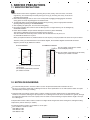
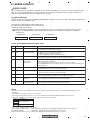
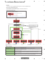
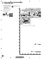
1
ORDER NO. CRT5370 DEH-X36UI/XNUC CD RDS RECEIVER DEH-X36UI /XNUC DEH-X3600UI DEH-X3650UI DEH-X3650UI DEH-X3650UI DEH-X3690UI /XNUC /XNCS /XNGS /XNGS1 /XNID This service manual should be used together with the following manual(s): Model No. CX-3287 Order No. CRT4759 Mech. Module S11.6STD Remarks CD Mech. Module : Circuit Descriptions, Mech. Descriptions, Disassembly PIONEER CORPORATION 1-1, Shin-ogura, Saiwai-ku, Kawasaki-shi, Kanagawa 212-0031, Japan PIONEER ELECTRONICS (USA) INC. P.O. Box 1760, Long Beach, CA 90801-1760, U.S.A. PIONEER EUROPE NV Haven 1087, Keetberglaan 1, 9120 Melsele, Belgium PIONEER ELECTRONICS ASIACENTRE PTE. LTD. 253 Alexandra Road, #04-01, Singapore 159936 PIONEER CORPORATION 2013 K-ZZZ JULY 2013 Printed in Japan 1 2 3 4 SAFETY INFORMATION CAUTION This service manual is intended for qualified service technicians; it is not meant for the casual do-it-yourselfer. Qualified technicians have the necessary test equipment and tools, and have been trained to properly and safely repair complex products such as those covered by this manual. Improperly performed repairs can adversely affect the safety and reliability of the product and may void the warranty. If you are not qualified to perform the repair of this product properly and safely, you should not risk trying to do so and refer the repair to a qualified service technician. A WARNING This product may contain a chemical known to the State of California to cause cancer, or birth defects or other reproductive harm. Health & Safety Code Section 25249.6 - Proposition 65 B Where in a manufacturer’s service documentation, for example in circuit diagrams or lists of components, a symbol is used to indicate that a specific component shall be replaced only by the component specified in that documentation for safety reasons, the following symbol shall be used: - Safety Precautions for those who Service this Unit. When checking or adjusting the emitting power of the laser diode exercise caution in order to get safe, reliable results. Caution: 1. During repair or tests, minimum distance of 13 cm from the focus lens must be kept. 2. During repair or tests, do not view laser beam for 10 seconds or longer. C CAUTION: USE OF CONTROLS OR ADJUSTMENTS OR PERFORMANCE OF PROCEDURES OTHER THAN THOSE SPECIFIED HEREIN MAY RESULT IN HAZARDOUS RADIATION EXPOSURE. CAUTION This product is a class 1 laser product classified under the Safety of laser products, IEC 60825-1:2007. D WARNING! The AEL (accessible emission level )of the laser power output is less than CLASS 1 but the laser component is capable of emitting radiation exceeding the limit for CLASS 1. A specially instructed person should do servicing operation of the apparatus. E Laser diode characteristics Wave length : 785 nm to 814 nm Maximum output : 1 190 µW(Emitting period : unlimited) Additional Laser Caution Transistors Q101 in PCB drive the laser diodes. When Q101 is shorted between their terminals, the laser diodes will radiate beam. If the top cover is removed with no disc loaded while such short-circuit is continued, the naked eyes may be exposed to the laser beam. F 2 DEH-X36UI/XNUC 1 2 3 4 5 6 7 8 CAUTION A Danger of explosion if battery is incorrectly replaced. Replaced only with the same or equivalent type recommended by the manufacturer. Discord used batteries according to the manufacturer's instructions. B C D E F DEH-X36UI/XNUC 5 6 7 8 3 1 2 3 4 CONTENTS SAFETY INFORMATION..................................................................................................................................... 2 1. SERVICE PRECAUTIONS ............................................................................................................................... 5 1.1 SERVICE PRECAUTIONS ........................................................................................................................ 5 1.2 NOTES ON SOLDERING .......................................................................................................................... 5 2. SPECIFICATIONS ............................................................................................................................................ 6 2.1 SPECIFICATIONS ..................................................................................................................................... 6 2.2 DISC/CONTENT FORMAT ........................................................................................................................ 9 3. BASIC ITEMS FOR SERVICE........................................................................................................................ 10 3.1 CHECK POINTS AFTER SERVICING..................................................................................................... 10 3.2 PCB LOCATIONS .................................................................................................................................... 10 3.3 JIGS LIST .................................................................................................................................................11 3.4 CLEANING................................................................................................................................................11 4. BLOCK DIAGRAM.......................................................................................................................................... 12 5. DIAGNOSIS.................................................................................................................................................... 14 5.1 OPERATIONAL FLOWCHART ................................................................................................................ 14 5.2 ERROR CODE LIST ................................................................................................................................ 15 5.3 CONNECTOR FUNCTION DESCRIPTION ............................................................................................. 18 6. SERVICE MODE ............................................................................................................................................ 19 6.1 DISPLAY TEST MODE 1 ......................................................................................................................... 19 6.2 DISPLAY TEST MODE 2 ......................................................................................................................... 20 6.3 SOFTWARE VERSION UP METHOD ..................................................................................................... 21 6.4 CD TEST MODE ...................................................................................................................................... 22 7. DISASSEMBLY .............................................................................................................................................. 23 8. EACH SETTING AND ADJUSTMENT ........................................................................................................... 29 8.1 CD ADJUSTMENT................................................................................................................................... 29 8.2 CHECKING THE GRATING AFTER CHANGING THE PICKUP UNIT.................................................... 30 8.3 PCL OUTPUT CONFIRMATION.............................................................................................................. 32 9. EXPLODED VIEWS AND PARTS LIST.......................................................................................................... 33 9.1 PACKING ................................................................................................................................................. 34 9.2 EXTERIOR............................................................................................................................................... 36 9.3 CD MECHANISM MODULE..................................................................................................................... 38 10. SCHEMATIC DIAGRAM............................................................................................................................... 40 10.1 TUNER AMP UNIT (GUIDE PAGE) ....................................................................................................... 40 10.2 KEYBOARD UNIT.................................................................................................................................. 46 10.3 CD CORE UNIT (S11.6VA) .................................................................................................................... 48 10.4 WAVEFORMS ........................................................................................................................................ 50 11. PCB CONNECTION DIAGRAM.................................................................................................................... 52 11.1 TUNER AMP UNIT................................................................................................................................. 52 11.2 KEYBOARD UNIT .................................................................................................................................. 56 11.3 CD CORE UNIT (S11.6VA) .................................................................................................................... 58 12. ELECTRICAL PARTS LIST .......................................................................................................................... 60 A B C D E F 4 DEH-X36UI/XNUC 1 2 3 4 5 6 7 8 1. SERVICE PRECAUTIONS 1.1 SERVICE PRECAUTIONS A 1. You should conform to the regulations governing the product (safety, radio and noise, and other regulations), and should keep the safety during servicing by following the safety instructions described in this manual. 2. Before disassembling the unit, be sure to turn off the power. Unplugging and plugging the connectors during power-on mode may damage the ICs inside the unit. 3. To protect the pickup unit from electrostatic discharge during servicing, take an appropriate treatment (shorting-solder) by referring to "the DISASSEMBLY". 4. After replacing the pickup unit, be sure to check the grating. 5. Be careful in handling ICs. Some ICs such as MOS type are so fragile that they can be damaged by electrostatic induction. 6. Notes about installation and pin number description of Power IC (IC301: PA2032A) The Power IC, PA2032A used on tha Tuner Amp Unit is a 25 pin IC. The same PCB of the Tuner Amp Unit is used for other models that use a 27 pin IC, too. So, the PCB has lands for a 27 pin IC. When you replace the Power IC, install the Power IC onto 25 pins (2- 26 pin) located in the center of 27 pins for IC301. B Therefore, when you check the Power IC on the block diagram, the schematic diagram and the PCB connection diagram, you have to pay attention as follows. BLOCK DIAGRAM SCHEMATIC DIAGRAM 12 (11) No connection 1 2 3 4 5 6 7 8 9 10 11 12 13 14 15 16 17 18 19 20 21 22 23 24 25 No connection 13 (12) 10 (9) 8 (7) 6 (5) 4 (3) 23 (22) H-SW 2 (1) 26 (25) OFF.DET The pin number is a number on the PCB (silk printing). The number in parentheses means the pin number of IC itself. The pin number of left side is a number on the PCB (silk printing). C The pin number of right side (in the IC frame) means the pin number of IC itself. D 1.2 NOTES ON SOLDERING For environmental protection, lead-free solder is used on the printed circuit boards mounted in this unit. Be sure to use lead-free solder and a soldering iron that can meet specifications for use with lead-free solders for repairs accompanied by reworking of soldering. E Compared with conventional eutectic solders, lead-free solders have higher melting points, by approximately 40 C. Therefore, for lead-free soldering, the tip temperature of a soldering iron must be set to around 373 C in general, although the temperature depends on the heat capacity of the PC board on which reworking is required and the weight of the tip of the soldering iron. Compared with eutectic solders, lead-free solders have higher bond strengths but slower wetting times and higher melting temperatures (hard to melt/easy to harden). The following lead-free solders are available as service parts: Parts numbers of lead-free solder: GYP1006 1.0 in dia. GYP1007 0.6 in dia. GYP1008 0.3 in dia. DEH-X36UI/XNUC 5 6 F 7 8 5 1 2 3 4 2. SPECIFICATIONS 2.1 SPECIFICATIONS DEH-X36UI/XNUC, DEH-X3600UI/XNUC A General Signal-to-noise ratio ......... 94 dB (1 kHz) (IHF-A network) Number of channels ........ 2 (stereo) MP3 decoding format ...... MPEG-1 & 2 Audio Layer 3 WMA decoding format ..... Ver. 7, 7.1, 8, 9, 10, 11, 12 (2 ch audio) (Windows Media Player) WAV signal format ........... Linear PCM & MS ADPCM (Non-compressed) Power source ...................14.4 V DC (10.8 V to 15.1 V allowable) Grounding system ............Negative type Maximum current consumption ..................................10.0 A Backup current.................. 4.0 mA or less Dimensions (W × H × D): DIN Chassis ............................ 178 mm × 50 mm × 165 mm (7 in. × 2 in. × 6-1/2 in.) Nose ................................ 188 mm × 58 mm × 15 mm (7-3/8 in.× 2-1/4 in.× 5/8 in.) D Chassis ............................ 178 mm × 50 mm × 165 mm (7 in.× 2 in.× 6-1/2 in.) Nose ................................ 170 mm × 46 mm × 15 mm (6-3/4 in.× 1-3/4 in.× 5/8 in.) B USB Weight ............................. 1 kg (2.2 lbs) Audio Maximum power output ... 50 W × 4 70 W × 1/2 Ω (for subwoofer) Continuous power output ................................... 22 W × 4 (50 Hz to 15 000 Hz, 5 % THD, 4 Ω load, both channels driven) Load impedance .............. 4 Ω (4 Ω to 8 Ω allowable) Preout maximum output level ................................... 2.0 V Loudness contour ............ +10 dB (100 Hz), +6.5 dB (10 kHz) (volume: –30 dB) Equalizer (5-Band Graphic Equalizer): Frequency ........................ 80 Hz/250 Hz/800 Hz/2.5 kHz/ 8 kHz Equalization range ........... ±12 dB (2 dB step) Subwoofer (mono): Frequency ........................ 50 Hz/63 Hz/80 Hz/100 Hz/ 125 Hz/160 Hz/200 Hz Slope ...............................–12 dB/oct, –24 dB/oct Gain ................................ +6 dB to –24 dB Phase .............................. Normal/Reverse C D CD player System ............................Compact disc audio system Usable discs .................... Compact disc USB standard specification ................................... USB 2.0 full speed Maximum current supply ................................... 1 A USB Class ....................... MSC (Mass Storage Class) File system....................... FAT12, FAT16, FAT32 MP3 decoding format ...... MPEG-1 & 2 Audio Layer 3 WMA decoding format ..... Ver. 7, 7.1, 8, 9, 10, 11, 12 (2 ch audio) (Windows Media Player) WAV signal format ........... Linear PCM & MS ADPCM (Non-compressed) FM tuner Frequency range .............. 87.9 MHz to 107.9 MHz Usable sensitivity ............. 9 dBf (0.8 µV/75 Ω, mono, S/N: 30 dB) Signal-to-noise ratio ......... 72 dB (IHF-A network) AM tuner Frequency range .............. 530 kHz to 1 710 kHz Usable sensitivity ............. 25 µV (S/N: 20 dB) Signal-to-noise ratio ......... 62 dB (IHF-A network) CEA2006 Specifications Power output ................... 14 W RMS × 4 Channels (4 Ω and 1 % THD+N) S/N ratio .......................... 91 dBA (reference: 1 W into 4 Ω) Note Specifications and the design are subject to modifications without notice. E Securing the front panel The front panel can be secured with the supplied screw. F Screw (BPZ20P060FTC) (UC) (XXX7020) (Except UC) 6 DEH-X36UI/XNUC 1 2 3 4 5 6 7 8 DEH-X3650UI/XNCS A General Number of channels ........ 2 (stereo) MP3 decoding format ...... MPEG-1 & 2 Audio Layer 3 WMA decoding format ..... Ver. 7, 7.1, 8, 9, 10, 11, 12 (2 ch audio) (Windows Media Player) WAV signal format ........... Linear PCM & MS ADPCM (Non-compressed) Rated power source .........14.4 V DC (allowable voltage range: 12.0 V to 14.4 V DC) Grounding system ............Negative type Maximum current consumption ..................................10.0 A Backup current................. 4.0 mA or less Dimensions (W × H × D): DIN Chassis ............................ 178 mm × 50 mm × 165 mm Nose ................................ 188 mm × 58 mm × 15 mm D Chassis ............................ 178 mm × 50 mm × 165 mm Nose ................................ 170 mm × 46 mm × 15 mm Weight ............................. 1 kg Audio Maximum power output ... 50 W × 4 70 W × 1/2 Ω (for subwoofer) Continuous power output ................................... 22 W × 4 (50 Hz to 15 000 Hz, 5 % THD, 4 Ω load, both channels driven) Load impedance .............. 4 Ω (4 Ω to 8 Ω allowable) Preout maximum output level ................................... 2.0 V Loudness contour ............ +10 dB (100 Hz), +6.5 dB (10 kHz) (volume: –30 dB) Equalizer (5-Band Graphic Equalizer): Frequency ........................ 80 Hz/250 Hz/800 Hz/2.5 kHz/ 8 kHz Equalization range ........... ±12 dB (2 dB step) Subwoofer (mono): Frequency ........................ 50 Hz/63 Hz/80 Hz/100 Hz/ 125 Hz/160 Hz/200 Hz Slope ...............................–12 dB/oct, –24 dB/oct Gain ................................ +6 dB to –24 dB Phase .............................. Normal/Reverse USB USB standard specification ................................... USB 2.0 full speed Maximum current supply ................................... 1 A USB Class ....................... MSC (Mass Storage Class) File system....................... FAT12, FAT16, FAT32 MP3 decoding format ...... MPEG-1 & 2 Audio Layer 3 WMA decoding format ..... Ver. 7, 7.1, 8, 9, 10, 11, 12 (2 ch audio) (Windows Media Player) WAV signal format ........... Linear PCM & MS ADPCM (Non-compressed) B FM tuner Frequency range .............. 87.5 MHz to 108.0 MHz Usable sensitivity ............. 9 dBf (0.8 µV/75 Ω, mono, S/N: 30 dB) Signal-to-noise ratio ......... 72 dB (IEC-A network) C AM tuner Frequency range .............. 531 kHz to 1 602 kHz (9 kHz) 530 kHz to 1 640 kHz (10 kHz) Usable sensitivity ............. 25 µV (S/N: 20 dB) Signal-to-noise ratio ......... 62 dB (IEC-A network) Note Specifications and the design are subject to modifications without notice. D CD player System ............................Compact disc audio system Usable discs .................... Compact disc Signal-to-noise ratio ......... 94 dB (1 kHz) (IEC-A network) E F DEH-X36UI/XNUC 5 6 7 8 7 1 2 3 4 DEH-X3650UI/XNGS, DEH-X3650UI/XNGS1 A General WAV signal format ........... Linear PCM & MS ADPCM (Non-compressed) Rated power source .........14.4 V DC (allowable voltage range: 12.0 V to 14.4 V DC) Grounding system ............Negative type Maximum current consumption ..................................10.0 A Backup current.................. 4.0 mA or less Dimensions (W × H × D): DIN Chassis ............................ 178 mm × 50 mm × 165 mm Nose ................................ 188 mm × 58 mm × 15 mm D Chassis ............................ 178 mm × 50 mm × 165 mm Nose ................................ 170 mm × 46 mm × 15 mm Weight ............................. 1 kg B USB USB standard specification ................................... USB 2.0 full speed Maximum current supply ................................... 1 A USB Class ....................... MSC (Mass Storage Class) File system....................... FAT12, FAT16, FAT32 MP3 decoding format ...... MPEG-1 & 2 Audio Layer 3 WMA decoding format ..... Ver. 7, 7.1, 8, 9, 10, 11, 12 (2 ch audio) (Windows Media Player) WAV signal format ........... Linear PCM & MS ADPCM (Non-compressed) Audio Maximum power output ... 50 W × 4 70 W × 1/2 Ω (for subwoofer) Continuous power output ................................... 22 W × 4 (50 Hz to 15 000 Hz, 5 % THD, 4 Ω load, both channels driven) Load impedance .............. 4 Ω (4 Ω to 8 Ω allowable) Preout maximum output level ................................... 2.0 V Loudness contour ............ +10 dB (100 Hz), +6.5 dB (10 kHz) (volume: –30 dB) Equalizer (5-Band Graphic Equalizer): Frequency ........................ 80 Hz/250 Hz/800 Hz/2.5 kHz/ 8 kHz Equalization range ........... ±12 dB (2 dB step) Subwoofer (mono): Frequency ........................ 50 Hz/63 Hz/80 Hz/100 Hz/ 125 Hz/160 Hz/200 Hz Slope ...............................–12 dB/oct, –24 dB/oct Gain ................................ +6 dB to –24 dB Phase .............................. Normal/Reverse C CD player D System ............................Compact disc audio system Usable discs .................... Compact disc Signal-to-noise ratio ......... 94 dB (1 kHz) (IEC-A network) Number of channels ........ 2 (stereo) MP3 decoding format ...... MPEG-1 & 2 Audio Layer 3 WMA decoding format ..... Ver. 7, 7.1, 8, 9, 10, 11, 12 (2 ch audio) (Windows Media Player) FM tuner Frequency range .............. 87.5 MHz to 108.0 MHz Usable sensitivity ............. 9 dBf (0.8 µV/75 Ω, mono, S/N: 30 dB) Signal-to-noise ratio ......... 72 dB (IEC-A network) MW tuner Frequency range .............. 531 kHz to 1 602 kHz (9 kHz) 530 kHz to 1 640 kHz (10 kHz) Usable sensitivity ............. 25 µV (S/N: 20 dB) Signal-to-noise ratio ......... 62 dB (IEC-A network) SW tuner Frequency range .............. 2 300 kHz to 7 735 kHz (2 300 kHz to 2 495 kHz, 2 940 kHz to 4 215 kHz, 4 540 kHz to 5 175 kHz, 5 820 kHz to 6 455 kHz, 7 100 kHz to 7 735 kHz) 9 500 kHz to 21 975 kHz (9 500 kHz to 10 135 kHz, 11 580 kHz to 12 215 kHz, 13 570 kHz to 13 870 kHz, 15 100 kHz to 15 735 kHz, 17 500 kHz to 17 985 kHz, 18 015 kHz to 18 135 kHz, 21 340 kHz to 21 975 kHz) Usable sensitivity ............. 28 µV (S/N: 20 dB) Signal-to-noise ratio ......... 62 dB (IEC-A network) Note Specifications and the design are subject to modifications without notice. E F 8 DEH-X36UI/XNUC 1 2 3 4 5 6 7 8 DEH-X3690UI/XNID General Rated power source .........14.4 V DC (allowable voltage range: 12.0 V to 14.4 V DC) Grounding system ............Negative type Maximum current consumption ..................................10.0 A Backup current.................. 4.0 mA or less Dimensions (W × H × D): DIN Chassis ............................ 178 mm × 50 mm × 165 mm Nose ................................ 188 mm × 58 mm × 15 mm D Chassis ............................ 178 mm × 50 mm × 165 mm Nose ................................ 170 mm × 46 mm × 15 mm Weight ............................. 1 kg WAV signal format ........... Linear PCM & MS ADPCM (Non-compressed) A USB USB standard specification ................................... USB 2.0 full speed Maximum current supply ................................... 1 A USB Class ....................... MSC (Mass Storage Class) File system....................... FAT12, FAT16, FAT32 MP3 decoding format ...... MPEG-1 & 2 Audio Layer 3 WMA decoding format ..... Ver. 7, 7.1, 8, 9, 10, 11, 12 (2 ch audio) (Windows Media Player) WAV signal format ........... Linear PCM & MS ADPCM (Non-compressed) B Audio Maximum power output ... 50 W × 4 70 W × 1/2 Ω (for subwoofer) Continuous power output ................................... 22 W × 4 (50 Hz to 15 000 Hz, 5 % THD, 4 Ω load, both channels driven) Load impedance .............. 4 Ω (4 Ω to 8 Ω allowable) Preout maximum output level ................................... 2.0 V Loudness contour ............ +10 dB (100 Hz), +6.5 dB (10 kHz) (volume: –30 dB) Equalizer (5-Band Graphic Equalizer): Frequency ........................ 80 Hz/250 Hz/800 Hz/2.5 kHz/ 8 kHz Equalization range ........... ±12 dB (2 dB step) Subwoofer (mono): Frequency ........................ 50 Hz/63 Hz/80 Hz/100 Hz/ 125 Hz/160 Hz/200 Hz Slope ...............................–12 dB/oct, –24 dB/oct Gain ................................ +6 dB to –24 dB Phase .............................. Normal/Reverse CD player System ............................Compact disc audio system Usable discs .................... Compact disc Signal-to-noise ratio ......... 94 dB (1 kHz) (IEC-A network) Number of channels ........ 2 (stereo) MP3 decoding format ...... MPEG-1 & 2 Audio Layer 3 WMA decoding format ..... Ver. 7, 7.1, 8, 9, 10, 11, 12 (2 ch audio) (Windows Media Player) FM tuner Frequency range .............. 87.5 MHz to 108.0 MHz Usable sensitivity ............. 9 dBf (0.8 µV/75 Ω, mono, S/N: 30 dB) Signal-to-noise ratio ......... 72 dB (IEC-A network) MW tuner Frequency range .............. 531 kHz to 1 602 kHz (9 kHz) 530 kHz to 1 640 kHz (10 kHz) Usable sensitivity ............. 25 µV (S/N: 20 dB) Signal-to-noise ratio ......... 62 dB (IEC-A network) C SW tuner Frequency range .............. 2 300 kHz to 7 735 kHz (2 300 kHz to 2 495 kHz, 2 940 kHz to 4 215 kHz, 4 540 kHz to 5 175 kHz, 5 820 kHz to 6 455 kHz, 7 100 kHz to 7 735 kHz) 9 500 kHz to 21 975 kHz (9 500 kHz to 10 135 kHz, 11 580 kHz to 12 215 kHz, 13 570 kHz to 13 870 kHz, 15 100 kHz to 15 735 kHz, 17 500 kHz to 17 985 kHz, 18 015 kHz to 18 135 kHz, 21 340 kHz to 21 975 kHz) Usable sensitivity ............. 28 µV (S/N: 20 dB) Signal-to-noise ratio ......... 62 dB (IEC-A network) D Note Specifications and the design are subject to modifications without notice. E 2.2 DISC/CONTENT FORMAT F DEH-X36UI/XNUC 5 6 7 8 9 1 2 3 4 3. BASIC ITEMS FOR SERVICE 3.1 CHECK POINTS AFTER SERVICING A To keep the product quality after servicing, please confirm following check points. No. 1 4 Procedures Confirm whether the customer complain has been solved. If the customer complain occurs with the specific media, use it for the operation check. Play back a CD. (Track search) Check FM/AM tuner action. (Seek, Preset) Switch band to check both FM and AM. Check whether no disc is inside the product. 5 Appearance check 2 CD 3 FM/AM tuner B Item to be confirmed The customer complain must not be reappeared. Display, audio and operations must be normal. No malfunction on display, audio and operation. Display, audio and operations must be normal. The media used for the operating check must be ejected. No scratches or dirt on its appearance after receiving it for service. See the table below for the items to be checked regarding audio: Item to be checked regarding audio Distortion Noise Volume too low Volume too high Volume fluctuating Sound interrupted C D 3.2 PCB LOCATIONS C CD Core Unit (S11.6VA) A Tuner Amp Unit A:DEH-X36UI/XNUC B:DEH-X3600UI/XNUC C:DEH-X3650UI/XNCS E:DEH-X3650UI/XNGS F:DEH-X3650UI/XNGS1 G:DEH-X3690UI/XNID Unit Number : QWM3628(A,B) Unit Number : QWM3629(C) Unit Number : QWM3630(E,F) Unit Number : QWM3631(G) Unit Name : Tuner Amp Unit Unit Number : Unit Name : Keyboard Unit Unit Number : CWX4269 Unit Name : CD Core Unit(S11.6VA) E B Keyboard Unit F 10 DEH-X36UI/XNUC 1 2 3 4 5 6 7 8 3.3 JIGS LIST - Jigs List Name 16P FFC Test Disc L.P.F. A Jig No. GGD1310 TCD-782 Remarks Tuner Amp Unit - CD Core Unit Checking the grating Checking the grating (Two pieces) Grease No. GEM1024 GEM1043 Remarks CD Mechanism Module CD Mechanism Module - Grease List Name Grease Grease B C 3.4 CLEANING D Before shipping out the product, be sure to clean the following portions by using the prescribed cleaning tools: Portions to be cleaned CD pickup lenses Cleaning tools Cleaning liquid : GEM1004 Cleaning paper : GED-008 E F DEH-X36UI/XNUC 5 6 7 8 11 1 2 3 4 4. BLOCK DIAGRAM A ANTENNA A TUNER AMP UNIT JA401 DACOUTL 1 5 16 2,3 18 57 FMMIXIN1 A :DEH-X3 B :DEH-X3 C :DEH-X3 E :DEH-X3 F :DEH-X3 G :DEH-X3 PINDIN LNAIN FM/AM TUNER IC401 TDA7706 I2CSCL I2CSDA RSTN 34 93 33 94 31 88 TUN_SCL RESET IC671 S-80827CNMC-B8M TUN_SDA TUNRES B 39 RES 1 VDD OUT 2 VDD3.3V JA891 56 WIRED REMOTE 2 KEYAD KEYAD 105 3 KEYD KEYD 1 GND SYSTEM MICRO COMPUTER IC601 (1/2) R5S726A0D216FP FLASH ROM IC681 A B :PEB106A8 C E F G :PEB103A8 ILMPW Q871 B.UP ILM+B Q872 VCC VDD3.3V iPod CP IC531 337S3959 C SCL SDA RST 19 ILMPW Q531 8 25 6 91 2 92 7 24 CPPWR CP_SCL CP_SDA REGULATOR IC IC911 BA49183-V12 CPRST 6 SW5V 9 SWVDD 7 VDD3.3V 8 VDD1.2V 5 SYS+B SW5V SWVDD VDD VDDCONT BSENS SYSPW SW5VCNT C PICKUP UNIT (P11)(SERVICE) 7 Q101 LD LD+ +B SYS+B 10 10 VDD V+3A 1 MD MD 11 11 2 PD LD PUEN VDD USB5V 5 8 8 FOM FOCUS ACT. TRACKING ACT. 93 FOP 3 3 2 2 TOP 1 TOM 4 IC301 BD8223EFV 1 TOP 4 TOM 8 9 SOP M REFOUT OC SOM LCOP LCOM CN701 VDD TD,FD VCC 5 118 LX EN 6 98 SYNC DDON FB BST 3 119 4 120 USBCTL USBFLG CN701 9 9 VDD VDD3.3V 55 FCO+ VD VD FCO23 40 22 41 MUTE 21 39 CNT SLLDO+ SLLDO- 35 S903 DSCSNS VDSENS 2 2 1 1 B.UP Q752 CLCONT 85 LOEJ 2 VDCONT CONT RESET 29 8 8 RESET 33 DSCSNS HOME CD DATA (CDSRQ,CDSTBY,SKIP, SCL,SDA,DATA,BCLK,LRCK,WAIT) S901 HOME VD Q751 CD DATA (CDSRQ,CDSTBY,SKIP, SCL,SDA,DATA,BCLK,LRCK,WAIT) DEH-X36UI/XNUC 1 SYSTEM COMP IC6 (2 R5S726A MECHA VD 3 SPO+ 2 SPO- 5 4 VDD TKO- RESET 12 B.UP 10 IC201 PEQ094A 38 F 1 1 7 TKO+ LDIN LOADING/CARRIAGE MOTOR 4 PD SD,MD 10 M SYSPW Q601 4 ACTUATOR/ MOTOR DRIVER FOM FOP 7 SPINDLE MOTOR BSENS AC,BD,VC,E,F HOLOGRAM UNIT E VOUT VIN EN REFO SWVDD 3 SYNC 54 REFO VREF 8 B.UP IC552 BD2232G-G Q102 LD 8 IC551 BD9876EFJ RF AMP, CD DECODER DIGITAL SERVO/DATA • PROCESSOR CPU V+3A 90 2 USB5V REGULATOR CD CORE UNIT(S11.6 VA) CN101 7 VCC 113 1 VDD12 +BUP D 11 3 4 CDRST 5 6 7 8 A ELECTRONIC VOLUME/ SOURCE SELECTOR IC201 PM9013A A :DEH-X36UI/XNUC B :DEH-X3600UI/XNUC C :DEH-X3650UI/XNCS E :DEH-X3650UI/XNGS F :DEH-X3650UI/XNGS1 G :DEH-X3690UI/XNID JA251 PL 35 OUTPL INAN1L PL 3 PREOUT 40 TUNL RCAG 1 FL FL 6 RCAG 4 Q251 P251 Q252 B 3.3V EVOL_LRCK EVOL_BCK EVOL_DATA EVOL_DT EVOL_CK EVOL_CS EVOL_RST 81 19 104 20 103 21 106 22 110 23 108 24 111 25 87 26 AUXL 37 JA901 MCLK LRCLK FUSE 10A 18 17 15 B.UP B.UP BCLK DIN OUTFL DATA OUTRL 33 12(11) 34 13(12) CLK FLIn RLIn FL+ MUTE STB Q301 (1/2) RESETB INBP4L 10(9) FL+ 8(7) FL- POWER AMP FLIC301 6(5) RL+ PA2032A RL+ 4(3) RL- RL- 1 3 5 7 Q301 (2/2) MUTE ANTPW 117 23(22) 17 2(1) H-SW MUTE BREM 26(25) 14 POWER SUPPLY EVOL_MCK C OFF.DET ASENS Q941 90 8 B.UP SWVDD ASENS ACC 13 BSENS SYSPW B SYSTEM MICRO COMPUTER IC601 (2/2) R5S726A0D216FP CN801 AUXL SSENS SOURCE 35 KEYBOARD UNIT JA1921 CN1931 19 19 18 18 FRONT AUX 113 89 AUXR 3 AUXL 2 AUXL SORUCE S1842 SOURCE MULTI-CONTROL AUXGND 1 4 2 3 1 S1830 ROT0 ROT1 53 ROT0 54 ROT1 6 6 4 4 ROT0 2 5 KDT2 ROT1 1 4 KST1 D 3 118 SYNC ILM+B 5 5 ILM+B SWVDD 3 3 SWVDD P04 P05 P06 Q601 P07 98 DDON KYDT DPDT 119 120 KYDT 22 8 8 10 10 20 20 99 KYDT 2 4 DPDT P01 LCD DRIVER/ KEY CONTROLLER IC1802 100 URX/P35 PDC202B IC801 TC7SET08FUS1 23 P00 UTX/P34 DPDT P02 P03 94 KDT0 95 KDT1 96 KDT2 97 KDT3 90 KST0 91 KST1 92 KST2 93 KST3 KEY MATRIX USBCTL USBFLG DSENS 34 DSENS LCD V1802 DSENS ILM+B RGB DRIVER IC1851 BH2228FV AO4 98 RMIN/P73/INT/T0IN REMOTE CONTROL SENSOR Q1852 (1/2) IC1941 PNJ4833M 1 E 4 Q1853 (1/2) 55 VDSENS RED LCD AO5 5 GREEN LCD Q1853 (2/2) UP RGBDT/DIMMER RGBCS/ILMCLR2 RGBCK/ILMCLR1 RGBDT 15 RGBST/ILMCLR2 11 RGBCK/ILMCLR1 7 14 12 7 14 12 RGBDT 12 RGBST 10 RGBCK 11 BLUE LCD DI CSB RED Key AO6 Q1851 (1/2) CLK GREEN Key BLUE Key VDCONT AO1 33 6 Q1859 1 Q1858 Q1857 Q1868 Q1867 Q1866 Q1851 (2/2) CDRST AO2 AO3 USB5V DM DP 49 DM 50 DP 11 11 13 13 15 15 2 Q1852 (2/2) D1885, D1886 3 ILM+B USB5V ILM+B USB5V DM DP DP 6 7 F CN1911 DM DEH-X36UI/XNUC 5 D1882, D1883, D1884 8 2 3 USB 85 21 4 13 1 2 3 4 5. DIAGNOSIS 5.1 OPERATIONAL FLOWCHART A Power ON Vcc : Pin 12, 20, 43, 78, 86, 109 PVcc : Pin 3, 16, 28, 36, 48, 69, 82,101, 112 Vcc = 1.2 V PVcc = 3.3 V BSENS B Pin 90 BSENS = L ASENS Pin 89 ASENS = L DSENS Pin 34 C DSENS = L Starts communication with Grille microcomputer. D 300 ms SWVDD <- H Pin 113 300 ms Source keys operative In case of the above signal, the communication with Grille microcomputer may fail. If the time interval is not 300 msec, the oscillator may be defective. E Source ON SYSPW <- H Pin 8 Completes power-on operation. (After that, proceed to each source operation) F 14 DEH-X36UI/XNUC 1 2 3 4 5 6 7 8 5.2 ERROR CODE LIST ERROR CODES If a CD memory device is inoperable, or operation of such media is stopped by an error, the error mode is established and a cause of the error is displayed by an error code. Indication of error codes is intended to reduce the number of calls from customers and facilitate failure analysis and repair work in servicing. A (1) DISPLAY METHOD If “0xFD” error mode is displayed in CD MODE (CD MODE area for display), an error code will be displayed in the MIN (minute display) and SEC (second display) areas. The same code is displayed in the MIN and SEC areas. The TNO area is blank (#0FFH), as it conventionally was. • Display example of the head unit Depending on the display capability of LCDs, the display format varies, as shown below. XX denotes an error number. Note: In a case of an OEM product, the error display format is subject to the specifications used by the equipment manufacturer. 8-digit display 6-digit display ERROR-xx ERR-xx B 4-digit display E-xx (2) LIST OF CD ERROR CODES (Error Mode: 0xFD) Code Classification Error code to be displayed 07 Servo TOC reading NG Details and possible causes TOC information cannot be read. --> The partial disk or TOC content is illegal. C 10 Servo Carriage Home NG The pickup cannot move toward the inner track. The CRG cannot move from the inner track. --> Defective HOME SW; Failure in CRG movement. Focusing not available --> Disc placed upside-down; Stains on the disc; excessive vibration. 11 Servo Focus NG 12 Servo Spindle Lock NG Subcode NG RF-amp NG Spindle not locked. Subcode not readable. Proper RF AMP gain not obtained. --> Defective spindle; Scratches or stains on the disc; excessive vibration. --> A CD-R/RW disc that does not contain data loaded, or in a rare case, disc placed upside-down. --> RF signal error. 15 Servo RF NG The digital signal from the disc cannot be detected. --> A CD-R/RW disc that does not contain data loaded. 17 Servo Setup NG The laser output cannot be adjusted. Focus can be easily lost. --> Scratches or stains on the disc; excessive vibration. 30 Servo Search Time Out Failed to reach a target address. And, the search became a timeout. --> Carriage/Tracking error; Scratches on the disc; Stains on the disc 50 Mechanism Load NG Eject NG Disc loading/ejection not completed --> A foreign object inserted in the mechanism; Disc jammed. 51 Mechanism Failure in retried turning for ejection Disc could not be ejected even after disc turning had been retried. --> A foreign object inserted in the mechanism; Disc jammed. D E NOTES • Indications of error codes are available only during disc operations, because CD operations are unavailable if a mechanical error is generated. • If the TOC cannot be read, It stops because of error 07. • If you design a new head unit, be sure to use one of the display formats indicated in “Display example of the head unit.” • The 2 high-order digits of an error code denote the main classification, shown below. code classification 0x 1x Servo-related errors 3x 5x Mechanism-related errors • How to restore from each error is shown below. Servo-related errors(0X, 1X, 3X) : Servo-related errors CD Off, Eject, ACC Off, Back-up Off, Communication reset, Reset Load NG/Eject NG(50) : Reload, Eject, ACC Off, Back-up Off, Communication reset, Reset Failure in retried turning for ejection : CD On, Eject, ACC Off, Back-up Off, Communication reset, Reset DEH-X36UI/XNUC 5 6 7 F 8 15 1 A 2 Symptoms are written in bold and causes in regular, non-indented text. Regular, indented text is used to indicate actions to be taken. 4 USB storage device/iPod FORMAT READ Sometimes there is a delay between the start of playback and when you start to hear any sound. Wait until the message disappears and you hear sound. Common AMP ERROR B 3 This unit fails to operate or the speaker connection is incorrect; the protective circuit is activated. Check the speaker connection. If the message fails to disappear even after the engine is switched off/on, contact your dealer or an authorized Pioneer Service Station for assistance. NO AUDIO There are no songs. Transfer the audio files to the USB storage device and connect. The connected USB storage device has security enabled. Follow the USB storage device instructions to disable the security. CD player SKIPPED ERROR-07, 11, 12, 17, 30 C The disc is dirty. Clean the disc. The connected USB storage device contains DRM protected files. The protected files are skipped. The disc is scratched. Replace the disc. PROTECT ERROR-07, 10, 11, 12, 15, 17, 30, A0 All the files on the connected USB storage device are embedded with DRM. Replace the USB storage device. There is an electrical or mechanical error. Turn the ignition switch OFF and back ON, or switch to a different source, then back to the CD player. ERROR-15 The inserted disc is blank. Replace the disc. D N/A USB The connected USB device is not supported by this unit. Connect a USB Mass Storage Class compliant device. Disconnect your device and replace it with a compatible USB storage device. ERROR-23 CHECK USB Unsupported CD format. Replace the disc. FORMAT READ Sometimes there is a delay between the start of playback and when you start to hear any sound. Wait until the message disappears and you hear sound. E NO AUDIO The inserted disc does not contain any playable files. Replace the disc. SKIPPED PROTECT All the files on the inserted disc are embedded with DRM. Replace the disc. 16 CHECK USB The connected USB storage device consumes more than maximum allowable current. Disconnect the USB storage device and do not use it. Turn the ignition switch to OFF, then to ACC or ON and then connect only compliant USB storage devices. CHECK USB The inserted disc contains DRM protected files. The protected files are skipped. F The USB connector or USB cable has shortcircuited. Check that the USB connector or USB cable is not caught in something or damaged. The iPod operates correctly but does not charge. Make sure the connection cable for the iPod has not shorted out (e.g., not caught in metal objects). After checking, turn the ignition switch OFF and back ON, or disconnect the iPod and reconnect. DEH-X36UI/XNUC 1 2 3 4 5 6 7 ERROR-19 MAINTENANCE Communication failed. Perform one of the following operations. –Turn the ignition switch OFF and back ON. –Disconnect the USB storage device. –Change to a different source. Then, return to the USB source. Pandora system is undergoing maintenance. Try again later. SKIP LIMIT iPod failure. Disconnect the cable from the iPod. Once the iPod’s main menu is displayed, reconnect the iPod and reset it. CHECK APP 8 A Skip limit reached. Do not exceed the skip limit. Due to music licensing restrictions, Pandora limits the total number of skips per hour. B This version of the Pandora application is not supported. Connect a device that has a compatible version of the Pandora application installed. ERROR-23 USB storage device was not formatted with FAT12, FAT16 or FAT32. USB storage device should be formatted with FAT12, FAT16 or FAT32. CHECK DEVICE Device error message displayed in Pandora application. Unable to play music from Pandora. Please check your connected device. ERROR-16 The iPod firmware version is old. Update the iPod version. C NO STATION iPod failure. Disconnect the cable from the iPod. Once the iPod’s main menu is displayed, reconnect the iPod and reset it. No station found. Create a station in the Pandora application on your connected device. NO ACTIVE ST STOP No station selected. Select a station. There are no songs in the current list. Select a list that contains songs. STATION FULL NOT FOUND A new station cannot be added. Delete an old station to open a spot for a new one. No related songs. Transfer songs to the iPod. D CAN.T DELETE Pandora The station could not be deleted. Run the same command for another station. ERROR-19 Communication failed. Disconnect the cable from the device. Once the device’s main menu is displayed, reconnect the device and reset it. NO NETWORK The connected device is out of area. Connect the connected device to a network. E NO SERVICE START UP APP The connected device is out of area. Connect the connected device to a network. The Pandora application has not started running yet. Start up the Pandora application. CAN.T PLAY INOPERABLE The operation was disabled. Run the same command for another station. The operation was disabled. Run the same command for another track. Apps TRY AGAIN START UP APP Unable to save thumb rating. Unable to save BookMark. Unable to add station. Try again later. DEH-X36UI/XNUC 5 F The application has not started running yet. Follow the instructions that appear on the screen. 6 7 8 17 1 2 3 4 5.3 CONNECTOR FUNCTION DESCRIPTION A B WIRED REMOTE CONTROL ANTENNA INPUT 15 13 11 9 7 5 3 1 FRONT OUTPUT 16 14 12 10 8 6 4 2 C 1 2 3 4 5 6 7 8 9 10 11 12 13 14 15 16 FL+ FR+ FLFRRL+ RR+ RLRR- REAR OUTPUT or SUBWOOFER OUTPUT NC NC NC NC ACC B.REM B.UP GND D E F 18 DEH-X36UI/XNUC 1 2 3 4 5 6 7 8 6. SERVICE MODE 6.1 DISPLAY TEST MODE 1 A [How to enter Test mode] Press and hold "MIX" and "LIST" buttons together, and turn BUP and ACC on. SOURCE LIST MIX B BAND ROTARY Grille condition Conf. item All light up All light off Conf. LCD pattern 1 (* And change ILM color) Conf. LCD pattern 2 Operate MIX + LIST SOURCE Show LCD Draw 1 No light Draw2 RGB White No light BAND Draw 3 Red ROTARY center Draw 4 Green C Drawings Style Draw1 ALL light up Draw2 ALL light off Draw3 D Draw4 E F DEH-X36UI/XNUC 5 6 7 8 19 1 2 3 4 6.2 DISPLAY TEST MODE 2 A The information such as the system microcomputer version is checked. [How to enter Test mode] Press and hold "1" and "3" buttons together, and turn BUP and ACC on. [Operation key] Operation key Processing 1+3 Enter display test mode Switch to next test mode Remarks B [Test items] Start display test mode. Press and hold "1" and "3" buttons together, and turn BUP and ACC on. Key Illumination Icon Off All off On (an initial value) All off * Initial condition System Version information is displayed. C S $ $ $ $ # # # $ PD number For PEA010A, "010A" is displayed # System microcomputer version For Ver.7.01, "701" is displayed On (an initial value or setting value of default menu) All off D Switching to next display by pressing “ 1 ” + “ 3 ” buttons together. Display is normally updated Product operation is performed as usual, in appearance. On (an initial value or setting value of default Switching to next display menu) by pressing “ 1 ” + “ 3 ” buttons together. E On (lighting condition of normal times) Display update is stopped The screen gets still when entering this item. Switching to next display by pressing “ 1 ” + “ 3 ” buttons together. On (an initial value or setting value of default menu) On (state when entering test mode) F 20 DEH-X36UI/XNUC 1 2 3 4 5 6 7 8 6.3 SOFTWARE VERSION UP METHOD Overview This mode is used for upgrading the MCU software of system using USB memory. A How to enter in USB rewriting mode Press and hold "1" and "2" buttons together, and turn BUP and ACC on. USB rewriting operation flow Explanatory note Screen display and ON/OFF of illumination Characters displayed on the screen USB Red frame: illumination lights up Gray frame: illumination lights off B Blue characters: operation to be carried out by a user of USB rewriting function Press and hold "1" and "2" buttons together, and turn BUP and ACC on. START UPDT Press LIST button * After connecting USB memory in which upgrading file is stored, press LIST button. (4) Retry count over Retry rewriting C As the reset is internally carried out, display and illumination go out Check of upgrading file is started (2) Upgrading file is not detected Upgrading file error CHECK FILE First time After retry Rewriting is started If the power supply is turned OFF during rewriting, retry the rewriting. DON'T STOP Switched every 5 seconds D (3) Rewriting failed PRG **/100 (1) Rewriting succeeded CAN'T UPDT COMPLETE Display is continued until the power supply is turned OFF In 5 seconds, usual operation (OFF SOURCE) FILE ERROR ERR->RETRY In 5 seconds, usual operation (OFF SOURCE) In 5 seconds, rewriting is retried ERR->RETRY In 5 seconds, rewriting is retried E Result of rewriting (1) Rewriting succeeded Displayed when USB rewriting is normally terminated. In 5 seconds, usual operation (OFF SOURCE) is started. (2) Upgrading file error Upgrading file is not detected Displayed when there is no upgrading file in USB memory or the data of upgrading file is different. In 5 seconds, usual operation (OFF SOURCE) is started. If the upgrading file error is detected or the upgrading file is not detected after the rewriting is retried, the rewriting is failed. In 5 seconds, rewriting is retried. (3) Rewriting failed Displayed when the writing of upgrading file in serial Flash is not normally terminated. Or, displayed if the upgrading file error is detected or the upgrading file is not detected after the rewriting is retried. In 5 seconds, rewriting is retried. (4) Retry count over Displayed when the retry becomes unavailable because the retry count is exceeded. The display is continued until the power supply is turned OFF. If the power supply is turned ON again, the display is not changed. The upgrading using USB is disabled, so it is necessary to write programs in serial Flash using E10A. DEH-X36UI/XNUC 5 6 7 8 F 21 1 2 3 4 6.4 CD TEST MODE - Flow Chart A To enter the test mode: [4] + [6] -> BUP + ACC ON [Key] [CD] or [SOURCE] Source ON TRK Contents MIN Display [BAND] [2] RF AMP *1 Gain switching TRK MIN SEC Power On (T.Offset is adjusted) TRK MIN SEC 00 B [BAND] MIN SEC [BAND] 91 91 SEC TRK MIN *2 TRK MIN SEC 0X 0X 0X [BAND] TRK MIN SEC [>] Tracking Servo Close 00 00 00 or 99 99 99 [3] SEC [1] Power Off GG ?? ?? ?? [3] F,T,RF AGC*5 F.Bias display switching TRK MIN SEC ?? ?? ?? [<] CRG - *6 00 00 00 or 99 99 99 *6 00 00 00 or 99 99 99 [<] CRG - 8X 8X 8X or 9X 9X 9X 8X 8X 8X or 9X 9X 9X [>] [<] CRG/TR Jump - *4 *4 TRK ?tr ?min ?sec ?tr ?min ?sec MIN SEC TRK MIN ?? T.Balance adjustment / T.BAL coefficient display TRK MIN SEC ?? ?? ?? SEC Tracking Open 8X 8X 8X or 9X 9X 9X Tracking Open 8X 8X 8X or 9X 9X 9X SEC t MIN SEC + 6 dB t TRK 06MIN06SEC06 + 12 dB TRK 12MIN12SEC12 D *2) Focus Close t TRK 00MIN00SEC00 (TRK99MIN99SEC99) S. Curve t 01MIN01SEC01 TRK F EQ measurement setting TRK 02MIN02SEC02 [Key] [BAND] [>] [<] [1] *3) F.Offset Display t RF.Offset t T.Offset Display t Switch to the order of the original display [2] [3] [6] *4) 100TR Jump E ?? [2] TYP TRK MIN ?tr ?min ?sec Power Off *1) ?? [2] CRG/TR Jump + F,T AGC / F.Bias RF AGC TRK MIN SEC Self-adjusting switching *3 MIN SEC TRK [2] CRG + [BAND] TRK [2] CRG + [>] RF AGC / RF AGC coefficient display TRK MIN SEC ?tr ?min ?sec C GG [1] Focus Mode switching [1] T.Close & AGC Applicable servomechanism Power Off MIN GG [6] Focus Close S curve check TRK MIN SEC 91 TRK 00 [3] Power Off TRK 00 Operation Test Mode Power On/Off CRG + / TR Jump + (Direction of the external surface) CRG - / TR Jump (Direction of the internal surface) T. CLS & AGC & Applicable servomechanism / AGC,AGC display setting RF Gain switching / Offset adjustment display / T.Balance adjustment / T. Open F. Close,S. Curve / Rough Servo and RF AGC / F,T,RF AGC F. Mode switching / Tracking Close *5) TRK/MIN/SEC t F.AGC t T.AGC Gain t F.Bias t RF AGC *6) CRG motor voltage = 2 [V] After the [EJECT] key is pressed keys other than the [EJECT] key should not be pressed, until disc ejection is complete. When the key [2] or [3] is pressed during the Focus Search, the power supply should be immediately turned off (otherwise the lens sticks to Wall, causing the actuator to be damaged). In the case of 100TR Jump, the mechanism shall be set to the Tracking Close mode when the key is released. When the power is turned on/off the gain of the RFAMP is reset to 0 dB. At the same time all the self-adjusting values shall return to the default setting. Do not do Tracking Servo Close before doing Focus Servo Close. (Because the overcurrent flows) F 22 DEH-X36UI/XNUC 1 2 3 4 5 6 7 8 7. DISASSEMBLY While the photograph shown is slightly different from this model in shape, the disassembly procedure is the same. A - Removing the Panel Assy (Fig.1) 1 1 Release the two latches. 2 Release the two latches and then remove the Panel Assy. 1 2 2 Panel Assy B Fig.1 - Removing the CD Mechanism Module (Fig.2) 1 Remove the screw. 2 Remove the two screws. 1 2 The CD Mechanism Module side is made a bottom. 2 C Heat Sink side 4 3 3 3 Push the area and remove the two hooks. 4 Slide the Tuner Amp Assy in the direction of the arrow. Tuner Amp Assy D CD Mechanism Module Lift off the Tuner Amp Assy from the Heat Sink side. 5 The Tuner Amp Assy is fixed into the ditch. 6 Disconnect the FFC and then remove the CD Mechanism Module. E 6 5 CD Mechanism Module F Fig.2 DEH-X36UI/XNUC 5 6 7 8 23 1 A 2 3 4 - Removing the Tuner Amp Unit (Fig.3) Tuner Amp Unit 1 Remove the two screws. 2 Remove the two screws and then remove the Tuner Amp Unit. 2 B 2 1 1 C Fig.3 - Attention of removing (Fig.4) D Don’t remove this screws excluding the dismantlement of the CD Mechanism Module. E CD Mechanism Module F Fig.4 24 DEH-X36UI/XNUC 1 2 3 4 5 6 7 8 - Disassembling the Panel Part (Fig.5, 6) A 1. Remove the arm while bending the rib of the panel upward. B Fig.5 2. Press the upside hook and the bottom side hook of the button at the same time, and pull out the button. C Fig.6 - Assembling the Panel Part (Fig.7, 8, 9) 1. Attach the button from the front side of the panel. D E Fig.7 2. Attach the spring to the arm as shown in the figure. The bended tip of the spring is set to this side. F Hitch the spring to the groove. DEH-X36UI/XNUC 5 6 7 Fig.8 8 25 1 2 3 4 3. Fit the spring in the groove at the position shown in the figure. A 4. Fit the boss on the lower side of the arm in the lower hole of the panel, and then warp the rib on the panel in the direction shown in the figure and fit the boss of the arm in the panel. B Fig.9 C D E F 26 DEH-X36UI/XNUC 1 2 3 4 5 6 7 8 How to carry the mecha unit A 1. Hold the designated points (shown with dashed lines) of the upper chassis and the front/rear bracket. 2. Be careful not to hold the solid line portions or the CRG mecha part or insert foreign substances, to prevent distortion. 3. When holding the sides of the upper chassis, do not apply excessive force to prevent distortion. (Approx. 8N or less) Handling OK B Handling NG C D E F DEH-X36UI/XNUC 5 6 7 8 27 1 2 3 4 How to remove the PU unit A 1. Create an empty-clamp state according to “How to create empty clamp state (motor drive)”. 2. Hook the feeding screw biasing spring to a tentative hooking portion (Fig 2b). Be careful not to get injured by the spring edge. 3. Hold the PU at the position A as shown in Fig 1. Slide the PU as far as possible toward the holder in the feeding screw so that a joint on the outer end of the feeding screw is loosened. 4. As shown in Fig 3, move the rear end of the feeding screw laterally and then upward, to remove it from the outer holder. 5. Lift the PU unit to disengage it from Part B of the chassis (Fig 4), and remove the PU unit. (Cautions) When re-installing the PU, be sure to first nip the chassis and the PU unit (Fig 4) at the position B. Also, make sure to fully hook the feeding screw biasing spring (Fig 2a). Please follow the service manual for adjustment of the PU unit after the re-installation. B Slide toward inner circumference Fig 2a Fig 2b Fig 1 Fully-hooked state C B Fig 3 Tentatively-hooked state The spring is below a resin flange and is built inside the sheet metal bending. A Fig 4 D Outer holder Rear end of feeding screw [Incorrect built-in state] The chassis is not nipped between the PU case and the PU rack. Normal built-in state E F 28 DEH-X36UI/XNUC 1 2 3 4 5 6 7 8 8. EACH SETTING AND ADJUSTMENT 8.1 CD ADJUSTMENT A 1) Cautions on adjustments In this product the single voltage (3.3 V) is used for the regulator. The reference voltage is the REFO1 (1.65 V) instead of the GND. If you should mistakenly short the REFO1 with the GND during adjustment, accurate voltage will not be obtained, and the servo’s misoperation will apply excessive shock to the pickup. To avoid such problems: a. Do not mix up the REFO1 with the GND when connecting the (-) probe of measuring instruments. Especially on an oscilloscope, avoid connecting the (-) probe for CH1 to the GND. b. In many cases, measuring instruments have the same potential as that for the (-) probe. Be sure to set the measuring instruments to the floating state. c. If you have mistakenly connected the REFO1 to the GND, turn off the regulator or the power immediately. Before mounting and removing filters or leads for adjustment, be sure to turn off the regulator. For stable circuit operation, keep the mechanism operating for about one minute or more after the regulator is turned on. 2) Test mode This mode is used to adjust the CD mechanism module. To enter the test mode. [4] + [6] -> BUP + ACC ON CD Source ON To exit from the test mode. Turn off the ACC and back up. Notes: a. During ejection, do not press any other keys than the EJECT key until the loaded disc is ejected. b. If you have pressed the [2] key or [3] key during focus search, turn off the power immediately to protect the actuator from damage caused by the lens stuck. c. For the TR jump modes except 100TR, the track jump operation will continue even if the key is released. d. For the CRG move and 100TR jump modes, the tracking loop will be closed at the same time when the key is released. e. When the power is turned off and on, the jump mode is reset to the single TR (91), the RF amp gain is set to 0 dB, and the auto-adjustment values are reset to the default settings. B C In the test mode, any software protections will not work. Avoid applying any mechanical or electrical shock to the mechanism during adjustment. The RFAGC and RFO signals with a wide frequency range are easy to oscillate. When observing the signals, insert a resistor of 1k ohms in series. The load and eject operation is not guarantied with the mechanism upside down. If the mechanism is blocked due to mistaken eject operation, reset the product or turn off and on the ACC to restore it. D E F DEH-X36UI/XNUC 5 6 7 8 29 1 2 3 4 8.2 CHECKING THE GRATING AFTER CHANGING THE PICKUP UNIT A Note : The grating angle of the PU unit cannot be adjusted after the PU unit is changed. The PU unit in the CD mechanism module is adjusted on the production line to match the CD mechanism module and is thus the best adjusted PU unit for the CD mechanism module. Changing the PU unit is thus best considered as a last resort. However, if the PU unit must be changed, the grating should be checked using the procedure below. Purpose : To check that the grating is within an acceptable range when the PU unit is changed. Symptoms of Mal-adjustment : If the grating is off by a large amount symptoms such as being unable to close tracking, being unable to perform track search operations, or taking a long time for track searching. B Method : Measuring Equipment Measuring Points Disc Mode Oscilloscope, Two L.P.F. E, F, REFO1 TCD-782 TEST MODE CD CORE UNIT C L.P.F. F E E Xch 100 kohm REFO1 Oscilloscope 390 pF VREF D Ych F 100 kohm VREF 390 pF L.P.F. Checking Procedure 1. In test mode, load the disc and switch the 3 V regulator on. 2. Using the > and < buttons, move the PU unit to the innermost track. 3. Press key 3 to close focus, the display should read "91". Press key 2 to implement the tracking balance adjustment the display should now read "81". Press key 3. The display will change, returning to "81" on the fourth press. 4. As shown in the diagram above, monitor the LPF outputs using the oscilloscope and check that the phase difference is within 75 . Refer to the photographs supplied to determine the phase angle. 5. If the phase difference is determined to be greater than 75 try changing the PU unit to see if there is any improvement. If, after trying this a number of times, the grating angle does not become less than 75 then the mechanism should be judged to be at fault. Note Because of eccentricity in the disc and a slight misalignment of the clamping center the grating waveform may be seen to "wobble" ( the phase difference changes as the disc rotates). The angle specified above indicates the average angle. Hint Reloading the disc changes the clamp position and may decrease the "wobble". E F 30 DEH-X36UI/XNUC 1 2 3 4 5 6 Grating waveform 7 8 Ech -> Xch 20 mV/div, AC Fch -> Ych 20 mV/div, AC 0 degrees A 30 degrees B 45 degrees 60 degrees C D 75 degrees 90 degrees E F DEH-X36UI/XNUC 5 6 7 8 31 1 2 3 4 8.3 PCL OUTPUT CONFIRMATION A - PCL Output In the normal operation mode (with the detachable panel installed, the ACC switched ON, the standby mode cancelled), shift the TESTIN IC601(Pin 99) terminal to H. The clock signal is output from the PCL terminal IC601(Pin115). The frequency of the clock signal is 600 kHz that is divided by 20th of the oscillation frequency of X601 (12MHz). The clock signal should be 600 kHz(- 25 Hz, + 25 Hz). If the clock signal is out of the range, the X'tal (X601) should be replaced with new one. B C D E F 32 DEH-X36UI/XNUC 1 2 3 4 5 6 7 8 9. EXPLODED VIEWS AND PARTS LIST NOTES : Parts marked by " * " are generally unavailable because they are not in our Master Spare Parts List. The > mark found on some component parts indicates the importance of the safety factor of the part. Therefore, when replacing, be sure to use parts of identical designation. Screw adjacent to mark on the product are used for disassembly. For the applying amount of lubricants or glue, follow the instructions in this manual. (In the case of no amount instructions,apply as you think it appropriate.) A " B C D E F DEH-X36UI/XNUC 5 6 7 8 33 1 2 3 4 9.1 PACKING A X3600UI/XNUC X3650UI/XNCS X3650UI/XNGS X3650UI/XNGS1 X3690UI/XNID B X36UI/XNUC A C X3600UI/XNUC X3650UI/XNCS X3650UI/XNGS X3650UI/XNGS1 X3690UI/XNID X3600UI/XNUC X3650UI/XNCS X3650UI/XNGS X3650UI/XNGS1 X3690UI/XNID D A E X3650UI/XNCS X3650UI/XNGS X3650UI/XNGS1 X3690UI/XNID X36UI/XNUC X3600UI/XNUC X36UI/XNUC X3600UI/XNUC X3600UI/XNUC X3650UI/XNCS X3650UI/XNGS X3650UI/XNGS1 X3690UI/XNID F 34 DEH-X36UI/XNUC 1 2 3 4 5 6 7 8 (1) PACKING SECTION PARTS LIST Mark No. Description Mark No. Part No. Part No. 10 Screw TRZ50P080FTC See Contrast table (2) 11 Unit Box See Contrast table (2) Protector See Contrast table (2) 12 Contain Box See Contrast table (2) Protector See Contrast table (2) 13 Card Remote Control Unit QXE1047 14 Case Assy See Contrast table (2) 15-1 Owner's Manual See Contrast table (2) 1 Cord Assy CDP1480 2 Polyethylene Bag See Contrast table (2) 3 Protector 4 5 6 Description Screw See Contrast table (2) 7 Polyethylene Bag CEG1160 8 Screw See Contrast table (2) * 15-2 Warranty Card See Contrast table (2) 9 Handle QNC3021 * 15-3 Service Network See Contrast table (2) (2) CONTRAST TABLE DEH-X36UI/XNUC, DEH-X3600UI/XNUC, DEH-X3650UI/XNCS, DEH-X3650UI/XNGS, DEH-X3650UI/XNGS1 and DEH-X3690UI/XNID are constructed the same except for the following: Description DEH-X36UI/ XNUC 2 3 4 5 6 Polyethylene Bag Protector Protector Protector Screw CEG1173 CHP4103 CHP4104 Not used BPZ20P060FTC CEG1173 Not used Not used CHP4594 BPZ20P060FTC QEG3001 Not used Not used CHP4594 Not used QEG3001 Not used Not used CHP4594 Not used QEG3001 Not used Not used CHP4594 Not used 8 11 12 14 15-1 Screw Unit Box Contain Box Case Assy Owner's Manual CRZ50P090FTC QHG3481 QHL3481 Not used QRD3201 CRZ50P090FTC QHG3480 QHL3480 Not used QRD3201 Not used QHG3482 QHL3482 QXA3129 QRD3202 Not used QHG3483 QHL3483 QXA3129 QRD3203 Not used QHG3484 QHL3484 QXA3129 QRD3203 15-2 15-3 Warranty Card Service Network QRY3001 Not used QRY3001 Not used Not used Not used Not used Not used CRY1394 CRY1395 Mark * * No. Mark * * No. Description DEH-X3600UI/ XNUC DEH-X3650UI/ XNCS DEH-X3650UI/ XNGS A B DEH-X3650UI/ XNGS1 C DEH-X3690UI/ XNID 2 3 4 5 6 Polyethylene Bag Protector Protector Protector Screw QEG3001 Not used Not used CHP4594 Not used 8 11 12 14 15-1 Screw Unit Box Contain Box Case Assy Owner's Manual Not used QHG3485 QHL3485 QXA3129 QRB3343 15-2 15-3 Warranty Card Service Network CRY1304 CRY1305 D E Owner's Manual,Installation Manual Part No. Language QRD3201 English, French, Spanish(Espanol) QRD3202 English, Spanish(Espanol), Portuguese(B) QRD3203 English, Traditional Chinese, Arabic, Persian QRB3343 English F DEH-X36UI/XNUC 5 6 7 8 35 1 2 3 4 9.2 EXTERIOR A B B A C D A E A F 36 DEH-X36UI/XNUC 1 2 3 4 5 6 7 8 (1) EXTERIOR SECTION PARTS LIST Mark No. > Description Mark No. Part No. Description Part No. 25 Spring CBH2210 BSZ26P080FTC 26 Button (EJECT) QAC3131 Screw BSZ26P120FTC 27 Button (DETACH) QAC3137 Cord Assy CDP1480 28 Button (MIX) QAC3138 29 Button (1-6) QAC3140 QBH3001 30 ••••• ••••• 1 Screw ASZ26P050FTC 2 Screw BSZ26P060FTC 3 Screw 4 5 6 Spring 7 Cover QNM3029 8 Panel QNS3126 31 9 Arm QNV3025 32 Cover QNS3615 10 Button QNV3026 33 Lighting Conductor QNV3074 34 Lighting Conductor QNV3075 11 CD Mechanism Module (S11.6VA)CXK5805 35 Segment LCD (V1802) CAW2041 12 FFC QDE3029 13 Case QNB3013 36 Holder QNC3068 14 Holder QNC3020 37 ••••• 15 Panel QNS3576 38 Lighting Conductor 39 Rubber Connector QNV3079 40 Knob Unit QXA3670 YBL5010 A B QNV3073 16 Tuner Amp Unit See Contrast table (2) 17 Screw BPZ26P080FTC 18 Screw BSZ26P060FTC 41 Spring 19 Screw BSZ26P120FTC 42 Button Unit QXA3946 20 Holder QNC3049 43 Grille Unit See Contrast table (2) 44 Door QAT3012 45 Card Remote Control Unit QXE1047 21 Heat Sink See Contrast table (2) 22 Fuse (10 A) YEK5001 23 Detachable Grille Assy See Contrast table (2) 46 Cover CNS7068 24 Screw BPZ20P100FTC 47 Cushion QNM3097 C (2) CONTRAST TABLE DEH-X36UI/XNUC, DEH-X3600UI/XNUC, DEH-X3650UI/XNCS, DEH-X3650UI/XNGS, DEH-X3650UI/XNGS1 and DEH-X3690UI/XNID are constructed the same except for the following: Mark No. Description 16 21 23 Tuner Amp Unit Heat Sink Detachable Grille Assy Grille Unit 43 Mark No. Description 16 21 23 Tuner Amp Unit Heat Sink Detachable Grille Assy Grille Unit 43 DEH-X36UI/ XNUC DEH-X3600UI/ XNUC DEH-X3650UI/ XNCS DEH-X3650UI/ XNGS DEH-X3650UI/ XNGS1 QWM3628 QNR3010 QXA3914 QWM3628 QNR3010 QXA3913 QWM3629 QNR3010 QXA3915 QWM3630 QNR3002 QXA3915 QWM3630 QNR3002 QXA3915 QXA3959 QXA3958 QXA3960 QXA3960 QXA3960 D DEH-X3690UI/ XNID QWM3631 QNR3002 QXA3916 E QXA3961 F DEH-X36UI/XNUC 5 6 7 8 37 1 2 3 4 9.3 CD MECHANISM MODULE A A B (A) (B) B (A) (B) C (A) (A) B C C (A) D (A) (A) D (A) (B) (A) (B) E A C (A) (A) : GEM1024 F (A) 38 (B) : GEM1043 DEH-X36UI/XNUC 1 2 3 4 5 6 7 8 CD MECHANISM MODULE SECTION PARTS LIST Mark No. Description Mark No. Part No. Description Part No. 50 Damper CNW1198 CBA1835 51 Arm CNW1726 Washer CBF1038 52 Motor Unit(M2)(LOAD/CRG) CXC4026 Spring CBH3010 53 Screw Unit CXC8894 54 Arm Assy CXE6232 55 Washer CBF1037 CBF1038 1 ..... 2 Screw BSZ20P040FTC 3 Screw(M2 x 4) 4 5 6 Spring CBH2855 7 Spring CBH2856 8 Spring CBH2860 56 Washer 9 Screw BSZ26P060FTC 57 Arm CND6242 10 Spring CBH3011 58 Collar CNW2444 59 Roller CNW2500 11 Coil Spring CBH3095 60 Gear Unit CXE6225 12 Spring CBH3014 13 Spring CBH3015 61 Washer YE15FTC 14 Spring CBH3016 62 Chassis Unit CXE4528 15 Spring CBH3017 63 Motor Unit(M1)(SPDL) CXE2273 64 Screw JFZ20P025FTC 65 Screw JGZ17P022FTC 16 Spring CBH3086 CBH3019 17 Spring 18 ..... 66 Screw EBA1028 19 Leaf Spring CBL1824 67 CD Core Unit (S11.6VA) CWX4269 20 PU Unit(P11)(Service) CXX4754 68 Chassis CNA3181 A B C 21 Bracket CND4553 22 Arm CND6406 23 Bracket CND6127 24 Bracket CND5710 25 Lever CND5398 26 Sheet CNN3678 27 Rack CNV8342 28 Guide CNW2240 29 Roller CNW1172 30 ..... 31 Arm CNW2241 32 Roller CNW1175 33 ..... 34 Arm CNW1177 35 Arm CNW1178 36 Gear CNW1180 37 Gear CNW1181 38 ..... 39 Gear CNW1183 40 Rack CNW1184 41 Gear CNW1185 42 Gear CNW1186 43 Gear CNW1187 44 Gear CNW2287 45 Clamper CNW1190 46 Arm CNW1192 47 Holder CNW1193 48 Holder CNW1194 49 Damper CNW1197 D E F DEH-X36UI/XNUC 5 6 7 8 39 1 2 3 4 10. SCHEMATIC DIAGRAM 10.1 TUNER AMP UNIT (GUIDE PAGE) A Note: When ordering service parts, be sure to refer to " EXPLODED VIEWS AND PARTS LIST" or "ELECTRICAL PARTS LIST". A-a VDIG VCCREG1V2 REG1V2 VREG3V3 RSTN RDSINT TUN_SDA CTF1786- L413 C465 C466 C468 C464 C461 TUN_SCL DGND 32 31 30 29 NM GND 10 6 SKIP 9 VDD 5 SCL 8 RESET 3 4 /CDSTBY 2 7 SDA VD VD /CDSRQ 1 DGND1 VDD4 RESET SCL SKIP SDA CDSRQ NM C709 CDSTBY 1k R710 R711 100 220 100 R708 R709 220 0.1u/10 D751 C752 DZ2J082M0 390 1/4 R752 R753 47k R705 C7 N NM C7 N R724 NM GND TUN_RST 1000p/50 DGND AGND CDRST CDSKIP CD_SDA CDSTBY CDSRQ CD_SCL FLASH ROM IC681 47k R684 47k MCLK CDWAIT VDCONT ASENS BSENS *2 1 8 CS VCC NC/SIO3 7 SO/SIO1 3 SCLK 6 WP/SIO2 4 5 GND SI/SIO0 2 KN1 47k DGND IC681 PEB106A8 PEB103A8 A, B C-G RESETB *2 RF GND C459 100p/50 *1 VDCONT VDSENS C440 C439 0.1u/16 C441 0 TUN_RST NM C435 0.47u/10 L411 NM R414 *1 3.3V *1 R413 8.2 1/4W 8.2 SW5V PEB106A8 M2R6TP_GND C622 0.1u/10 0.1u/10 85 22p/50 C625 C624 47k 98 DDON 99 TESTIN R647 STB 109 Vcc 0.1u/10 110 EVOL_DT R650 1k 111 SWVDD5 112 PVcc 0.1u/10 113 SWVDD 120 C620 220 R625 220 220 220 220 R627 R626 R628 220 R629 R631 R630 100 R632 47k 47k C621 0.1u/10 C623 0.1u/10 81 R633 82 VOUT D GND FLG 19 18 AUXR 17 AUXGND 16 DP RGBST/ILMCLR2 15 KYDT RGBDT/DIMMER ILMPW OFFSET RGBST/ILMCLR2 BTDATA BT_LRCK BT_BCK 2.2k DSENS BT_RST AUXL SOURCE R801 2.2k GND R803 22k R804 22k R805 100 R806 R807 100 100 11 L 14 44 DM 13 12 RGBCK/ILMCLR1 11 DPDT 10 USBGND 9 KYDT 8 RGBDT 7 6 CT US5V NM USB5V R818 CN1931 20 ROT0 5 A GRILLE DGND USBGND ILM GND DEH-X36UI/XNUC 3 4 VA801 EZJP0V270RM D811 NM NM D810 D809 DZ2S068C D808 DZ2S068C 0.1u/16 C808 D807 DZ2S068C C807 1u/10 D806 DZ2S068C NM D803 DZ2S068C D804 DZ2S068C NM C814 ILMG C806 0.1u/16 C803 NM USGND C804 NM NM DGND C805 1 D802 DZ2S068C DGND NM : No Mount NM 4 SWVDD 3 2 ILMGND C802 ROT1 DZ2S068C ILM+B D801 The > mark found on some component parts indicates the importance of the safety factor of the part. Therefore, when replacing, be sure to use parts of identical designation. B DEH-X36UI/XNUC DEH-X3600UI/XNUC DEH-X3650UI/XNCS DEH-X3650UI/XNGS DEH-X3650UI/XNGS1 DEH-X3690UI/XNID 220p/50 J DSENS VBUS RGBDT/DIMMER R802 C801 CN801 CKS6452- SYSPW USBCTL GND A B C E F G RGBCK/ILMCLR1 USBCLT DGND BTTX FLG BTRX 4 C813 OC NM EN D805 DZ2S068C GND R663 NM VIN C560 NM C561 1u/10 C569 NM C562 3 5 RGBDT IC552 BD2232G-G 1 NOTE : Symbol indicates a resistor. No differentiation is made between chip resistors and discrete resistors. Symbol indicates a capacitor. No differentiation is made between chip capacitors and discrete capacitors. MD_CLK 79 78 Vcc 77 QIO3 76 Vss 75 QIO2 74 QIO1 73 QIO0 72 QSSL 71 Vss 70 QSPCLK 69 PVcc 83 80 MD_BOOT EVOL_MCK 84 Vss PVcc VDCONT GND GND 2 2 /CDWAIT Vcc EVOL_RST BTTESTIN SYNC SYNC 0.1u/10 DDON EN C604 BST 10k R664 10k 5 R661 NM R653 GND SYNC USBCTL /USBFLG R603 3.3V 220u/16 C552 1u/16 C551 C565 CCG1222- C570 NM 6 MUTE 119 FLG VCC C563 SYNC RAM_MON C603 0.1u/10 EN FIN FB Vss PCL 118 SYNC 2.2k USBCTL 8 7 117 NM VC B.UP 4.7u BST R652 SYNC PCL 115 RAM_MON 116 0.1u/10 4 VCC MUTE NM 3 FB GND E C630 R601 NM VC Lx GND 9 EVOL_CS 114 C633 GND 2 CMS03 D551 EVOL_CK C629 1k NM NM C555 6800p/25 C554 R551 GND 6.8k 220u/6.3 C556 C557 1u/10 4.7u C564 CCG1201D552 RB056L-40 0 NM IC551 BD9876EFJ 1 LX 1u/10 C559 GND 180k D 470 R554 iPod CP@(2.0C) C553 0.01u/16 43k D NC3 R552 SCL C558 RST TP1 5 R555 6 4 R553 3 NC2 VCC R535 4.7k 7 R534 2.7k 8 PAD 9 C532 0.1u/10 1 USB&USB5V Vss 108 1k CP_SDA L551 CTH1524- EVOL_DATA R649 NM USB5V KEYD 106 R648 CPRST IC531 337S3959 105 107 100 A, B, C E, F G C602 CP_SCL R539 EVOL_LRCK R662 NM 100 100 EVOL_BCK 104 ROM NM R537 103 R651 47k R532 2.2k R540 R644 100 R645 100 47k CPPWR BT_TESTMD C601 4.7k 102 R602 DATA PVcc 0.1u/10 3 PVcc C631 22p/50 GND R533 2.2k D602 RB551VM-30 Vss 101 4 BT_BCK 5 Vss 6 BT_LRCK 7 BTDATA 8 SYSPW 9 ROM 10 Vss 11 RGBCK/ILMCLR1 12 Vcc 13 BTRX 14 BTTX 15 RGBCS/ILMCLR2 16 PVcc 17 ANTPW 18 Vss 19 ILMPW 20 Vcc 21 RGBDT/DIMMER 22 KYDT only A, B KEYD DIN CLK Q531 LSAR523UB R538 BT_TESTMD 22p/50 C628 100 0.1u/10 BCLK LRCLK IC601 R5S726A0D216FP *3 100k BTRST 1k NM R536 TESTIN R643 CP_SCL CP_SDA TUN_SCL C626 BT_TESTIN KEYD KEYAD 0.1u/16 C892 C891 CKS6437- C627 22p/50 KEYD2 KEYAD2 1k R892 TUNRES /CDSRQ 10k R891 KEYAD 89 CD_SDA R669 1 3 2 JA891 GND L531 90 CD_SCL CDSRQ 97 KEYD W.REM TUN_SDA 96 Q601 LTC014YEB 0.1u/16 D 94 95 DDON C894 1000p/50 C893 VA891 NM R893 NM 1000p/50 VA892 NM MIC1P MIC1N 6 5 4 3 2 1 93 CD_SDA 2 GND GND NM CD_SCL 1 C974 NM /ASENS 92 R641 R642 TUN_SDA 2.2k 91 CP_SDA TUN_SCL GND /BSENS CP_SCL 4.7k NM NM R973 47k 1 R972 BTRX R668 GND NM R646 2 BTTX R971 4.7k 3 BT_RST R639 4 MIC1N 47k R637 47k NM 47k 5 GND R636 BT_BCK R640 6 GND MIC1P BTDATA BT_LRCK L971 NM BTTOSYS 100 100 C972 7 100 R975 MIC1P MIC1N 8 SYSTOBT 47k 1 0.01u/16 86 9 R531 2 R704 100k R634 1k GND R974 R976 (W/R) 1 3 R703 4.7k R635 1k 10 NM 40 4 6 C701 JA892 F 5 8 87 BTLRCK GND C531 6 7 R638 12 NRST_CPU 0.1u/10 GN 5 RN4983 C973 47p/50 GND 13 NC1 1 88 GND 14 BTBCK 11 SDA 4 2 NM C971 VCC 15 2 3 BT Connector VCC 16 GND VDCONT Q752 GND NM CN971 (RMIC) C753 NM 0.27uH 1.5uH 0.39uH 2.2uH 330 360 0 390 NM 0.1u/10 0.01u/16 NM 1u/10 NM 1u/10 NM DCH1246 NM 0.01u/10 NM 10p/50 1u/10 C438 NM C468 28 27 NM C436 NM R410 34 *1 R412 C433 1000p/50 RFGND C442 0.1u/10 I2CSDA 33 C437 NM DGND C432 82p/50 I2CSCL 35 47k R702 100k L701 NM 36 CN7 R701 220 37 CTF1389 NM 4.7uH NM 47uH 390 470 NM 680 VD1 R707 38 Q751 KTD2092 R706 39 7.4V VD2 CCG1201-A-T 10u/10 C751 NM NM C446 NM C MECHA VD NM 8p/50 22p/50 2p/50 1u/10 0.47u/10 0.1u/16 NM 100p/50 1000p/50 NM 1u/10 0.1u/10 0.01u/16 0.1u/10 NM 68n NM 10k NM VKN1192- R682 GND C445 0.1u/10 C449 NM R417 C451 AMMIXIN2 26 LNADEC2 LNAIN2 LNAOUT2 AMMIXIN1 25 22 23 NM 24 R409 0 C427 0.1u/10 33 100p/50 47u *1 L415 CD CN701 NM NM DGND C BTDATA 62 R408 470 RF GND RF GND CCG1218C443 E, F, G 15p/50 0.01u/16 B.UP 1/4W C429 L410 L414 NM C467 0.1u/10 C444 SW Model C682 C458 RFGND DGND NM AGND RF GND 1000p/50 RFGND C431 NM 0.01u/16 C462 GND DGND C463 NM C459 C447 C448 C467 L405 L406 L407 L408 L409 L410 R403 R408 R409 R411 C445 0 No SW A, B, C NM NM 3p/50 NM 100p/50 82p/50 R681 C465 *1 *1 C434 *1 21 *1 L416 NM 40 VDD3V3 C430 680 NM 1u/10 R407 1M R404 C423 8p/50 R405 C466 C425 CCG119210u L409 0.39u NM C422 1M R406 C421 3p/50 0.01u/16 0.01u/16 L408 4.7u L407 0.27u C428 390 CTF1389 L405 68n C424 R403 C419 15p/50 L406 C420 0.01u/16 C428 C432 C435 C439 41 GND3V3 0.1u/10 GNDLNA C418 0.022u/16 LNADEC 16 RFGND LNAOUT TCAM2 15 CCG119210u PINDDEC PINDIN VCCVCO GND RFGND GPIO8 17 C416 NM C415 0.1u/10 CTF1786- GPIO7 LF1 LNAIN 14 LFREF TDA7706 18 C414 0.01u/16 NM 46 45 GNDVCO CK_SEL 20 C413 0.1u/10 A GND 12 13 RFGND L404 11 IC401 C460 10 R416 NM 47 2.2u 48 GPIO2 GPIO3 GPIO4 GPIO5 GPIO6 VCCRF R411 9 0.01u/16 *1 C420 C421 C423 DGND TEST 44 VDD_CORE GND1V2 43 GPIO0 42 GPIO1 TCAM 8 AGND R415 GNDRF 7 *1 C419 *1 L418 NM L417 FMPINDRV FMPINDDEC FMMIXIN1 6 C412 0.1u/10 C411 63 64 FMMIXIN2 19 C406 0.01u/16 0.01u/16 C405 C407 NM C408 0.01u/16 6p/50 C409 L402 0.15u C402 0.01u/16 C403 1u/10 AGND orRFGND C404 NM 2 FMMIXDEC 4 5 CTF1786- 0.1u/10 C401 0.1u/10 RFGND RF GND L403 C461 C417 3 TCFM 2 33p/50 *1 TVDAC 1 C426 750 RN731VN 220 L401 0.27u R402 C410 D402 R401 D401 B RN731VN Detailed page A-b 3 PLLTEST 61 GND-PLL 60 VCC-PLL 59 VCC-ADC_DAC 58 DACOUTR 57 DACOUTL 56 GND-ADC_DAC 55 VREFDEC 54 GND-REF 53 OSCOUT 52 OSCIN 51 VCC-REF VDDIO1V2 50 VDDPLL1V2 49 NM A-a X2 GND1 X1 CSS1848- 0.1u/10 1 C454 RFGND X401 36.48MHz 4 GND2 C448 0.1u/10 9p/50 9p/50 L419 CTF1786- DCH1246 C455 0.22u/16 C450 C464 1u/6.3 TUNL GNDSLINK M2R6TP_GND NM Guide page P402 3 C453 1 2 KN2 HSPC16701B02 P401 A-b TUNR C456 4700p/25 0.1u/10 C452 YKS5041- TUNGND A-a AGND L420 CTF1786- FM: -14.7 dBs AM: -14.5 dBs JA401 C457 4700p/25 C447 1u/10 *1 TUNER ANTENNA R754 Large size SCH diagram A-b 1u/10 A-a 5 6 7 8 A A-b 10u 22k C258 R258 100p/50 100p/50 22k R257 C257 1 Q252 5 4 C261 0.01u/10 NM C260 C259 100p/50 100p/50 0.1u/10 22k R254 R253 C254 RN1910 3 6 C334 NM C319 100p/50 1p/50 C320 C321 C326 C325 C324 13 14 15 16 17 18 19 20 21 22 23 24 25 No connection 1000p/50 10p/50 10p/50 10p/50 10p/50 ACC 10 9 RL2 RL1 FR2 FL2 FR1 FL1 RFGND FUSE YEK5001 8 7 TEL RRRL- 6 RR+ 5 RL+ 4 FR- 3 FL- 2 FR+ 1 FL+ C930 NM RFGND GND FM:+20.3 dBs AM:+20.5 dBs AUX:+35.3 dBs CD:+35.6 dBs USB:+35.7 dBs E 0.1u/16 C941 1k 47k R942 R879 1.2k ASENS NM TELIN D951 L951 15k BTH1101DAN202UM GND C969 GND 6 CCG1192-A 10u R310 GND 0 D302 NM Dim off 12.13 V Dim on 8.03 V ILM GND NM B.REM&A.ANT C961 RGBDT/DIMMER GND ROT0 NM ILMPW C322 0.1u/16 R873 NM C968 5 RN4983 (10A) 11 D301 DZ2J075M0 4 1 17 12 NM C913 1000p/50 C912 1000u/16 0.1u/16 C914 R911 1 CCG1201-A 4.7u C915 NM C917 1000p/50 C916 D912 > R944 3.3k (1/10W) D871 R874 390 NM D872 R875 DPDT 8.2k H-SW 12 NM 3 Q875 LTC043EEB KYDT R815 NM 1608 C328 47k 1SR154-400 GND R951 2 47k NM 0.1u/16 C871 R876 NM 47k C872 0.1u/16 2.2k 2.2k 9 15 B.UP 14 BREM &A.ANT 13 ACC RR1 1k Q874 R878 RGBCK/ILMCLR1 8 11 16 GND 11 VDDCONT 12 GND CRG03 D941 DZ2J068M0 TELIN LED Supply B.UP1 BREM RR2 22k Q951 LSAR523UB Q873 2SD1767(QR) D902 TELIN 4.7u CCG1201-A C918 SYS+B SWVDD NM C919 CCG1201-A C920 NM C921 CCG1201-A C922 4.7u 4.7u ASENS1 22k R943 Q941 LSCR523UB R941 B.UP3 1SR154-400 D911 CRG03 10k R872 ASENS2 GND2 D901 R953 NM GND1 L901 R952 NM C873 2.2k 7 10 D 9 SWVDD 10 +BUP GND R871 600uH 2 1 CTH1432- GND R812 6 FL+ JA901 GND R605 CDSCKIN NM C925 1 R912 1000p/50 C926 RESET NM C923 4 CCG1201-A C924 NC1 NM 5 VDD VSS VDDCNT 22k NC2 C929 OUT R914 SWVDD5 IC671 Q872 LTC143EUB DM C323 22k 1u/10 C335 NM R307 B.UP2 CDLRCKIN SSENS RGBST/ILMCLR2 5 FLP-GND1 18 7 VDD 8 VDD12 SWVDD ASENS 2.2k 27 5 SYS+B 6 SW5V 1.2V DGND R811 100p/50 C333 NM C332 NM C331 NM NM NM NM C312 C311 C310 C309 NM DSENS VDD 4.7u 1u/10 C672 NM C671 R311 NM C329 470 R304 470 470 470 R302 R303 R301 SW5V C928 3 DP R816 2.2k SYS+B B.UP SW5V 1.2V 15k 12MHz SSENS S-80827CNMC-B8M NM CDSTBY TELIN DPDT KYDT CPPWR R814 3 SW5VCNT 4 +B C911 4 D671 100k R810 R813 SYSPW 47k 47k R610 2 NM R671 R809 22 IC911 BA49183-V12 1 BSENS 2 SYSPW BSENS R913 NM C927 CDSCKIN Vss 2p/50 C673 1 RL+ VCC C Q302 NM GND CDDATAIN NM R606 31 30 29 PVcc TELIN CPPWR CDSTBY 27 26 NM 28 R670 NM NM R607 32 22 3 3 MUTE +B R877 CTF1713- NM SYSB AUXR AUXG 44 RN4983 22k AUXL 2 2 26 GND IC REGULATOR USB GND RST 4 R308 SYSPW RGB Supply L801 6 3 STBY 25 P-GND4 BSENS 2.2k 11 1 C607 22k 22k 5 GNDTP2 220 4 2 B.UP CCH2040GND 2200u/16 R306 2 RL- GND Q871 2SA1577(QR) CPRST RGBDT/DIMMER ILMPW OFFSET RGBST/ILMCLR2 BTTX BTRX RGBCK/ILMCLR1 R804 GND C314 0.1u/16 C901 CDRST R808 100 100 1u/16 OFFSET GND NM 33 C605 0.1u/10 R604 KYDT DPDT 24 23 34 RGBDT 0.1u/10 TELIN1 25 CPRST /CDRST /DSENS CDDADATIN CDLRCKIN R609 0.1u/10 DSENS1 R608 AC_GND C313 P-GND2 11 SVR 12 FLIn 13 RLIn 14 AGND 15 RRIn 16 FRIn 17 AC-GND 18 FR+ 19 P-GND3 20 FR21 VCC 22 RR+ 23 MUTE 24 RR- AGND 12p/50 C606 36 SSENS 35 22 RGBDT/DIMMER 21 Vss ILMPW ANTPW PVcc Vcc 20 19 18 17 C604 R603 R664 10k BTTX RGBCS/ILMCLR2 16 14 15 C603 0.1u/10 13 NM Vcc BTRX PVcc GND OFF.DET 1 POWER SUPPLY 38 10 GND No connection CKM1613CSS1847- X601 R611 C609 0.1u/10 1 X1 0.1u/10 NC2 C610 47k X2 3 NM 41 15k R660 R659 12p/50 NC1 2 C608 1.5k CKIO 37 Vss NM 0.1u/10 C611 PVcc R613 0.22u/16 Q301 GND NMI 42 Vss 40 RGBCK/ILMCLR1 NM DM Vcc 43 Vss MUTE DP R612 0.22u/16 C303 10k 3 RES 39 12 NM C615 47k C307 R305 ROT1 ROT0 47k 47 7 0.22u/16 MU1 CDSKIP PVcc 48 6 NM C327 R615 5 GNDTP1 9 10u/16 C318 0.22u/16 GND KEYAD DM 49 PLLVcc 11 C614 GND ASEMDR614 EXTAL 44 10 NM R616 47k DP 50 4 VDD1.2V NM R620 VDSENS ASEMD 51 Vss 46 0.1u/10 NM C617 C616 AGND 3 8 GND AGND 10k 47k MODEL RB751SM-40 R617 D601 R618 47k 0.1u/10 only A, B R619 58 KEYAD 56 VDSENS 55 Vss C602 Q251 MCLK LRCLK BCLK DIN DATA CLK STB RESETB AUXR TUNR TUNL C612 *3 NM STBY C317 C301 TRST 47k R622 R623 ASEBRK 47k TRST 61 59 MODELAD 57 R619 NM 47k 47k NM L602 C613 0.1u/10 XTAL 45 47k VDD3.3V NM R621 2 AMP R309 10k 60 R312 NM SYS+B 5.78 V C305 ROT0 53 100 GND 12p/50 5 6 7 TDI 3 TDO 4 TMS 2 64 65 R625 R626 R627 R628 R629 R630 63 TDO ASEBRK 62 TDI TCK TMS C620 0.1u/10 TCK 1 66 220 220 220 220 220 220 8 C622 22p/50 C621 0.1u/10 100 R632 47k 47k R633 R631 81 80 4 CSS1794- 16.9344MHz GND CDSKIP 52 R806 R807 GND IC301 PA2032A 2.2k *3 R805 820 GND2 C618 3X2 12p/50 ROT1 54 A, B, C E, F G R251 1 3.3V 47k C681 C619 2 AVref AVcc AVss R618 47k 22k NM C251 CCG12014.7u PREOUT 5 4 FR R313 L601 R5S726A0D216FP 820 CKB1099- 2 1 6 NM X1 1 2 DGND MD_CLK 79 78 Vcc 77 QIO3 76 Vss 75 QIO2 74 QIO1 73 QIO0 72 QSSL 71 Vss 70 QSPCLK 69 PVcc 68 AUDIO_X1 67 AUDIO_X2 MD_BOOT EVOL_MCK X603 GND1 3 R624 IC601 JA251 3 X602 CSS1603- 16.9344MHz 1 R683 47k C683 3p/50 NM R682 PEB106A8 PL PR FL 1 0.1u/10 47k R685 CS VCC NC/SIO3 7 SO/SIO1 3 SCLK 6 WP/SIO2 4 5 GND SI/SIO0 RCAG 2 R259 NM The pin number of right side (in the IC frame) means the pin number of IC itself. C682 AUXL AUXG CDSCKIN CDLRCKIN CDWAIT CDDATAIN CDSKIP CDRST CD_SDA CD_SCL CDSTBY CDSRQ 47k MCLK NM 8 CCG12014.7u FRch L681 IC681 > 3.0A P251 CEK1386- 820 R252 C252 FLch GND R255 22k NM PRch RR PR FR The pin number of left side is a number on the PCB (silk printing). R684 47k R681 FLASH ROM 2 R803 C255 CCG1201- 4.7u FR FL RR 1 AGND GND 1 820 MUTE 2 AGND USBGND B RL Set back chart R256 CCG12014.7u 6 NM USB GND ROR *2 C256 PLch ucomD RFGND GND C227 R723 NM RCA FM: -6.6 dBs AM: -6.4 dBs AUX:+9.3 dBs CD:+10.4 dBs USB:+10.6 dBs B.REM& 961 - 970 A.ANT BT MOD 971 - 990 3 C219 CCG1192- C218 47u/16 C224 0.1u/10 NM 2 10u DGND L201 RN1910 C223 1000p/50 AGND MECHA VD 751 - 800 GRILL 801 - 850 SWVDD5 851 - 870 ILMPW 871 - 890 W.REM&MIC 891 - 900 PW CONNECT 901 - 910 IC REG 911 - 940 ASENS 941 - 950 TELIN 951 - 960 RCA 251 - 300 AMP 301 - 400 TUNER 401 - 470 iPod CP 531 - 550 USB&USB5V 551 - 600 UCOM 601 - 670 RESET 671 - 680 FLASH ROM 681 - 690 DSENS 691 - 700 CD MECHA 701 - 750 C253 REFERENCE AREA MAP EVOL 201 - 250 DGND 21 22 23 0.1u/10 C215 24 25 26 0.1u/10 27 0.1u/10 NM C214 28 35 33 34 32 36 37 NM AGND DGND R722 NM NM TUNER AMP UNIT 4 R721 NM NM R724 A 6.8k NM C221 5 1u/10 NM NM C703 C201 C706 38 40 IC201 PM9013A 10p/50 10p/50 C702 L701 NM R705 C234 R704 100k 1u/10 DGND 1 INAN1R INAN1L 2 INAP2R INAP2L 3 INBN3R C205 INBN3L 1u/10 4 INBP4R C203 INBP4L 5 IN5R C226 IN5L 6 OUTPR NM OUTPL 7 OUTRR C232 OUTRL 8 OUTFR NM OUTFL C207 0.1u/10 9 AVDDR1 AGNDL1 C208 0.1u/10 10 AVDDR2 AGNDL2 C210 11 VREFR C209 10u VREFL 150p/50 CCG119212 AGNDR1 AVDDL1 13 AGNDR2 AVDDL2 14 DGND C229 DVDD2 10u 1000p/50 15 TEST C216 L202 RESETB CCG1192- CTF1793- 16 REG C228 STB C217 NM 17 DVDD1 CLK NM 18 DOUT 0.1u/10 C220 DATA C235 19 MCLK CCG1192DIN 10u 20 LRCLK BCLK 150 150 R715 R716 R717 220 100 1k R710 C704 10p/50 C705 R711 R709 R703 4.7k 100 1 R708 8 220 2 220 7 R707 3 R706 4 6 150 GND A GND 1u/10 100k 39 NM R719 5 C233 1u/10 C213 1u/10 C202 31 150p/50 NM PGND GND 29 C211 1u/10 C206 C710 220 R718 100k C204 C231 DGND PGND C212 CCG1192- PGND WAIT BCLK DATA DGND1 LRCK VDD4 SCL SKIP SDA RESET CDSRQ CDSTBY NM 47k R702 FM: -5.7 dBs AM: -5.5 dBs AUX:+9.3 dBs CD:+9.6 dBs USB:+9.7 dBs C236 30 NM C225 C708 R720 NM R701 RL FL 16 WAIT 13 LRCK ROL C707 NM 15 PGND 14 GND GND 12 BCLK 11 DATA 10 6 SKIP 9 VDD 5 SCL 8 RESET CN701 7 SDA VD C 4 /CDSTBY VD 2 1 KN1192- 3 N701 /CDSRQ CD C330 NM AGND GND ILMPW 2.2k ROT1 SWVDD L851 F 2 3 INB 5 Vcc INA GND OUTY 4 TC7SET08FUS1 C811 NM IC801 1 DPDT 0.1u/10 NM C851 4.7k R851 NM C852 C810 220p/50 VA802 EZJP0V270RM C809 220p/50 VA801 EZJP0V270RM D811 NM NM D810 D809 DZ2S068C 0.1u/16 D808 DZ2S068C C808 D807 DZ2S068C C807 1u/10 D806 DZ2S068C R817 GND GND A SWVDD GND DEH-X36UI/XNUC 5 6 7 8 41 VDD 9 GND 10 NM C702 GND DGND1 C 5 K 6 8 C 3 7 M NM C703 L701 NM C620 PVcc 69 QSPCLK 0.1u/10 0 11 DATA DATA 150 R715 R685 DGND 14 GND R618 47k 22k NM R619 NM 47k 47k AVref AVcc AVss C710 X602 CSS1603- 1 2 47 Vss 46 Vss PVcc 48 DM 49 DP 50 ASEMD 51 CDSKIP 52 ROT0 53 ROT1 54 KEYAD 56 VDSENS 55 MODELAD 57 58 59 60 3 16.9344MHz NM L681 R723 NM R722 NM R721 NM 10p/50 C706 10p/50 10p/50 C705 C704 100k GND C202 C206 2.2k 47k ASEMDR614 47k R616 47k R615 CSS1794- X603 AGND MODEL 0.1u/10 C612 1u/10 1u/10 1u/10 NM C233 47k R618 *3 USBGND NM 4 only A, B 12p/50 GND2 C618 X1 1 16.9344MHz 3X2 2 R624 12p/50 C619 GND1 C613 0.1u/10 NM PGND GND R719 220 12 BCLK BCLK 150 CDDATAIN R716 68 TUNL 13 LRCK LRCK 150 47k 8 TCK 1 40 15 PGND 7 IC201 PM9013A 16 WAIT TMS 2 NM C234 1 1u/10 C201 TUNR R717 AUDIO_X1 CDSCKIN R683 47k C683 3p/50 CDLRCKIN 39 2 PGND WAIT R718 CDWAIT 0.1u/10 6 C681 5 TDI 3 38 3 R619 6 NM C204 47k TDO 4 67 AUDIO_X2 66 TCK 65 TMS 64 TDI 63 TDO ASEBRK 62 37 AUXR 1u/10 C205 4 1u/10 C203 5 C226 D601 47k 36 C231 33 8 10k R623 ASEBRK 47k TRST 61 34 7 C232 RB751SM-40 R617 9 AGND NM C207 0.1u/10 DGND 26 GND GND NM NM R620 L602 NM NM R621 L601 ROR 23 DGND VDD3.3V VDD1.2V NM USB GND C227 24 10u C212 CCG119211 C210 NM C615 DGND R622 31 150p/50 10 C208 0.1u/10 C616 C614 10u C209 NM NM C617 12 150p/50 CCG1192NM C229 R659 TRST 35 NM 32 0.1u/10 C213 30 29 C211 0.1u/10 C214 28 0.1u/10 C215 27 13 INAN1R INAN1L INAP2R INAP2L INBN3R INBN3L INBP4R INBP4L IN5R IN5L OUTPR OUTPL OUTRR OUTRL OUTFR OUTFL AVDDR1 AGNDL1 AVDDR2 AGNDL2 VREFR VREFL AGNDR1 AVDDL1 AGNDR2 AVDDL2 DGND DVDD2 TEST RESETB 1000p/50 15k R660 22 DIN 25 STB DVDD1 DATA 21 MCLK BCLK LRCLK 20 CLK 17 REG 14 10u 15 C216 L202 CCG1192- CTF1793- 16 C228 C217 NM 15k DM DP CDSKIP ROT1 ROT0 VDSENS KEYAD MUTE AGND AGND DGND RR PR FR ucomD RFGND GND NM L201 DGND 1000p/50 C223 NM C221 AGND C218 47u/16 DOUT 18 NM 0.1u/10 C220 19 C235 CCG119210u MCLK LRCLK BCLK DIN DATA CLK STB RESETB CCG1192C219 1.2V C224 0.1u/10 B.UP PGND SYS+B 10u SW5V NM C225 1u/10 SYS+B 5.78 V 470 C236 R301 A GND R302 R720 NM FL 470 NM GND MUTE 6 1 4 5 RN4983 Q301 10k R305 2 3 C303 GND 220 R306 0.22u/16 C307 GND 0.22u/16 0.22u/16 C305 0.22u/16 FRch FLch PRch PLch C301 RCA 251 - 300 AMP 301 - 400 TUNER 401 - 470 iPod CP 531 - 550 USB&USB5V 551 - 600 UCOM 601 - 670 RESET 671 - 680 FLASH ROM 681 - 690 DSENS 691 - 700 CD MECHA 701 - 750 REFERENCE AREA MAP EVOL 201 - 250 FM: -5.7 dBs AM: -5.5 dBs AUX:+9.3 dBs CD:+9.6 dBs USB:+9.7 dBs 470 RL C309 NM ROL NM C310 AUXL AUXG C611 NM C311 C707 NM 0.1u/10 NM C312 C708 C256 820 AGND 1u/16 C313 GND CCH2040GND 2200u/16 C901 GND C314 0.1u/16 10k R309 R251 C251 820 820 R252 R255 CCG12014.7u CCG12014.7u C252 C255 CCG1201- 4.7u 820 MUTE R256 B.REM& 961 - 970 A.ANT BT MOD 971 - 990 CCG12014.7u MU1 A MECHA VD 751 - 800 GRILL 801 - 850 SWVDD5 851 - 870 ILMPW 871 - 890 W.REM&MIC 891 - 900 PW CONNECT 901 - 910 IC REG 911 - 940 ASENS 941 - 950 TELIN 951 - 960 C333 NM 6 A-a A-b R307 NM Q252 GND FR RR R259 NM FR FL PR PL RCAG NM Q302 GND AGND AC_GND 8 27 26 25 24 23 22 No connection H-SW 25 P-GND4 21 20 19 18 17 16 15 14 13 12 11 10 9 7 P-GND1 6 5 4 3 2 FL- VCC RL+ STBY RL- P-GND2 OFF.DET 1 No connection IC301 PA2032A FL+ 11 SVR 12 FLIn 13 RLIn 14 AGND 15 RRIn 16 FRIn 17 AC-GND 18 FR+ 19 P-GND3 20 FR21 VCC 22 RR+ 23 MUTE 24 RR- 10 GNDTP1 9 8 7 6 5 4 3 2 1 PREOUT CKB1099- JA251 NM GND GND 5 4 2 1 6 3 R312 STBY 2 NM B.UP GND 1 > P251 CEK1386- 3.0A Set back chart FL RL RCA 0.01u/10 R313 R308 GNDTP2 NM 10u/16 C318 C317 AMP GND FM: -6.6 dBs AM: -6.4 dBs AUX:+9.3 dBs CD:+10.4 dBs USB:+10.6 dBs TUNER AMP UNIT 1 6 N701 3.3V C331 NM C327 C332 NM 1u/10 C335 NM 4 22k C329 C334 NM 3 2 5 Q251 22k R257 R254 R253 1 4 3 R311 R258 22k 22k 22k R304 470 A-b NM 2 5 RN1910 RN1910 4 47k C258 C257 C254 C328 C319 C320 C321 C259 100p/50 100p/50 100p/50 C253 100p/50 NM 1608 100p/50 1p/50 100p/50 3 C323 DEH-X36UI/XNUC 10p/50 2 C260 1 C324 42 C261 F 0.1u/10 E 10p/50 D C325 C 3 10p/50 A C326 B 2 10p/50 1 4 The pin number of left side is a number on the PCB (silk printing). The pin number of right side (in the IC frame) means the pin number of IC itself. R303 RGBDT/DIMMER CTF1713- L801 3 3 2 2 CPRST 47 41 38 PVcc 36 CKIO 37 Vss RES 39 Vss 40 PLLVcc NMI 42 Vcc 43 EXTAL 44 XTAL 45 Vss 46 Vss PVcc 48 DM 49 2.2k R817 2.2k GND 2.2k 2.2k 0.1u/10 C610 GND 100k NM R671 DM DP AUXR AUXG AUXL SSENS SWVDD NM ROT1 ROT0 KYDT RGBCK/ILMCLR1 L851 1.5k R613 D671 RGBST/ILMCLR2 NM 0.1u/10 DSENS1 R608 C606 R611 C609 0.1u/10 47k NM R612 DGND SWVDD DPDT C607 VSS VDD OUT IC671 NC1 NC2 R606 R607 USB GND 12p/50 RESET S-80827CNMC-B8M 3 2 1 RST C608 12p/50 NM ILM GND NM R877 4 5 R659 NM 15k CDRST CDLRCKIN CDDATAIN GND Q873 2SD1767(QR) Q872 LTC143EUB GND GND INA Vcc OUTY IC801 INB 3 1 2 MUTE 4 5 SW5V 6 5 4 Dim off 12.13 V Dim on 8.03 V RN4983 Q874 LED Supply ASENS SWVDD5 SYSPW BSENS OFFSET Q875 LTC043EEB TC7SET08FUS1 3 2 1 ILMPW NM DPDT SSENS DSENS RGB Supply Q871 2SA1577(QR) GND DM DP CDSKIP ROT1 ROT0 GND C929 RGBDT/DIMMER ILMPW TELIN 22k R941 A-a A-b ASENS2 Q301 6 5 4 MUTE RN4983 IC REGULATOR GND 1 2 3 10k R305 ASENS1 GND D941 GND CCG1192-A 10u MU1 B.REM&A.ANT GND C969 C968 NM DZ2J068M0 220 R306 22k R914 22k R913 VDDCNT B.UP2 R952 1k R951 GND AGND NM C330 D302 NM 0 R310 C930 L951 15k BTH1101- R953 NM GND VCC MUTE RR+ 27 26 FM:+20.3 dBs AM:+20.5 dBs AUX:+35.3 dBs CD:+35.6 dBs USB:+35.7 dBs FL1 FR1 FL2 FR2 RL1 RR1 RL2 RR2 TELIN 25 24 23 22 21 20 (10A) RLRR+ RL+ FRFLFR+ FL+ 6 5 4 3 2 1 RR- TEL 7 8 9 10 11 12 15 B.UP 14 BREM &A.ANT 13 ACC YEK5001 FUSE > JA901 CKM1613- 16 GND 17 18 No connection H-SW RR25 P-GND4 24 23 22 B.UP1 ACC B.UP3 BREM GND2 GND D902 NM RFGND GND DAN202UM GND D951 D901 GND1 1SR154-400 GND Q302 NM NM R308 GNDTP2 1SR154-400 GND 2 1 CTH1432- L901 600uH TELIN RFGND ASENS 1k R944 22k Q951 LSAR523UB GND D912 D911 CRG03 11 VDDCONT 12 GND 9 SWVDD 10 +BUP 7 VDD 8 VDD12 5 SYS+B 6 SW5V 3 SW5VCNT 4 +B IC911 BA49183-V12 1 BSENS 2 SYSPW CRG03 SWVDD 1.2V VDD SW5V SYSB +B SYSPW BSENS CCH2040GND 2200u/16 7 8 A-b R812 R811 2.2k R816 2.2k R814 R813 22 R810 22 R809 2.2k R808 31 32 47k 47k 0.1u/10 DP 50 SSENS 35 /CDRST /DSENS 34 CDDADATIN 33 CDLRCKIN R619 NM 47k 47k PVcc R618 47k 22k NM Vss C611 ASEMDR614 NM ASEMD 51 C851 CDSKIP 52 CDSCKIN R615 47k 1u/10 ROT0 53 47k 2p/50 C673 X601 X2 3 NC2 4 NC1 2 1 X1 22k VDSENS B.UP R879 1.2k C323 10p/50 R616 47k 4.7u C DPDT 23 DPDT CPPWR 25 TELIN R670 26 CDSTBY 27 CDSTBY KYDT 22 KYDT EZJP0V270RM NM D811 CCG1201-A C922 C324 10p/50 ROT1 54 8.2k R610 C672 SYS+B NM C928 28 NM NM R604 TELIN NM NM C923 29 C605 0.1u/10 NM R605 CDSCKIN TELIN1 CPPWR C810 220p/50 30 R815 PVcc R851 R609 C671 C852 R912 1000p/50 C926 C925 4.7u 1 CCG1201-A C924 CSS18470.1u/16 C873 24 VA802 EZJP0V270RM 220p/50 C872 SWVDD NM C921 12MHz 47k R878 CPRST C809 NM SYS+B NM C919 47k NM C927 Q941 LSCR523UB 4.7u CCG1201-A C920 R942 CCG1201-A C918 4.7u C325 10p/50 KEYAD VDSENS 55 1000u/16 R307 R911 NM C917 1000p/50 C916 C327 R943 1 CCG1201-A 4.7u C915 1u/10 C335 NM 0.1u/16 C914 6.8k 15k R660 0.1u/16 C871 10k R875 NM NM DZ2J075M0 R871 NM R876 R872 3.3k (1/10W) NM D872 D871 R874 390 C913 1000p/50 C912 C941 NM C326 10p/50 AVss C811 1000p/50 0.1u/16 C911 3.3V 0.1u/10 7 47k 1.2V R873 NM DEH-X36UI/XNUC C961 6 NM 5 NM 6 D301 mber of IC itself. C322 0.1u/16 5 8 POWER SUPPLY A B C D E 43 F 4.7k KN2 C410 *1 33p/50 RFGND 2 RFGND L405 68n C466 L407 0.27u CTF1389 C419 15p/50 L406 1u/10 1 GND (W/R) (RMIC) NM JA892 2 MIC1N 5 GND 3 6 BTTOSYS GND 7 SYSTOBT 4 8 MIC1P 9 GND NRST_CPU 6 5 4 3 2 1 BTLRCK 10 BTBCK 11 BTDATA 12 GND 13 GND 14 VCC 15 VCC 16 NM CN971 R976 C973 47p/50 GND C462 GND R973 NM L971 MIC1P MIC1N C974 NM TCAM2 VCCVCO LF1 LFREF *1 NM 0.01u/16 GND *1 47u C429 L410 DGND GND 1000p/50 RFGND C431 NM C430 2 3 DGND C433 34 35 36 37 38 39 40 41 42 43 44 45 46 I2CSDA 33 I2CSCL VDD3V3 GND3V3 GPIO8 GPIO7 DGND *1 KEYD 0 *1 *1 DGND 0.1u/10 C442 NM CCG1218C443 R892 R891 DGND AGND RF GND C459 100p/50 KEYAD L411 NM R413 8.2 1/4W R414 *1 8.2 R412 R415 0 L414 NM C467 48 0.1u/10 C444 47 2.2u *1 NM R416 NM L418 NM L417 AGND *1 TEST VDD_CORE GND1V2 GPIO0 GPIO1 GPIO2 GPIO3 GPIO4 GPIO5 GPIO6 DGND 1/4W 1000p/50 RFGND 1 3 2 X2 GND1 X1 CSS1848- *1 JA891 W.REM RF GND C463 NM NM GND R972 NM R971 GND 2.2k 100 100 100 R975 R974 TDA7706 CK_SEL PINDDEC PINDIN FMPINDRV FMPINDDEC 1 4 GND2 IC401 GNDVCO X401 1k 1k TUN_RST TUN_SDA TUN_SCL NM L415 L416 NM TUNL 36.48MHz TUNR VCCRF TCAM GNDRF FMMIXIN1 FMMIXIN2 FMMIXDEC C425 CCG119210u 16 15 RF GND 0.01u/16 C424 BT Connector NM DGND *1 *1 L408 4.7u 390 R403 C418 0.022u/16 CCG119210u 14 C415 13 0.01u/16 12 11 10 9 8 7 6 5 4 3 2 1 NM C454 C414 0.01u/16 C412 0.1u/10 C411 AGND C455 0.22u/16 1u/10 AGND orRFGND C404 NM C402 0.01u/16 C403 C401 RFGND 0.1u/10 RFGND C458 RFGND DGND NM AGND RF GND C465 0.01u/16 FM: -14.7 dBs AM: -14.5 dBs A GND RFGND C420 0.01u/16 GND CTF1786- L404 CTF1786- RF GND L403 1 L401 0.27u 3 YKS5041- JA401 HSPC16701B02 P401 C456 4700p/25 56 C457 4700p/25 VCC-PLL ANTENNA 220 RN731VN 9p/50 C451 M2R6TP_GND 1M R406 C446 TUNGND 0.1u/10 6p/50 P402 750 D402 R402 RN731VN C406 R401 D401 L402 0.15u C461 C417 C408 0.01u/16 C413 C416 C409 NM C421 3p/50 GNDLNA 17 *1 KEYD2 KEYAD2 C465 C466 C468 C464 C461 C459 C447 C448 C467 L405 L406 L407 L408 L409 L410 R403 R408 R409 R411 C445 C428 C432 C435 C439 C420 C421 C423 C419 E, F, G 15p/50 0.01u/16 SW Model KEYD KEYAD BTRX BTTX BT_RST BT_LRCK BT_BCK BTDATA B.UP NM 0.27uH 1.5uH 0.39uH 2.2uH 330 360 0 390 NM 0.1u/10 0.01u/16 NM 1u/10 NM 1u/10 NM DCH1246 NM 0.01u/10 NM CTF1389 NM 4.7uH NM 47uH 390 470 NM 680 NM 8p/50 22p/50 2p/50 1u/10 0.47u/10 0.1u/16 NM 100p/50 1000p/50 NM 1u/10 0.1u/10 0.01u/16 0.1u/10 NM 68n NM A, B, C NM NM 3p/50 NM 100p/50 82p/50 No SW BCLK LRCLK DDON CDSRQ 3.3V *2 NM R642 Q601 LTC014YEB only A B 22p/50 C628 C627 22p/50 CD_SDA CD_SCL TUN_SDA TUN_SCL CP_SDA CP_SCL SW5V VD2 MECHA VD A, B C-G NM R641 BT_TESTMD R645 100 R644 100 0.1u/10 C626 100k TESTIN R643 M2R6TP_GND KN1 7.4V EVOL_LRCK KEYD 105 EVOL_BCK BT_TESTMD PVcc Vss TESTIN DDON /CDSRQ CD_SDA CD_SCL TUN_SDA 104 103 102 101 100 99 98 97 96 95 94 93 92 91 47k 47k R637 R636 6 5 2 1 4 3 RN4983 VDCONT Q752 Q751 KTD2092 IC681 PEB106A8 PEB103A8 GND CCG1201-A-T 10u/10 C751 NM C464 1u/6.3 18 NM L420 CTF17860.1u/10 C452 LNADEC 51 DCH1246 C453 LNAIN 0.1u/10 0.1u/10 C422 1u/10 64 TVDAC 63 TCFM 62 PLLTEST 61 GND-PLL 60 LNAOUT 20 LNAIN2 21 0.1u/10 R407 0.01u/16 L419 C428 0.01u/16 C405 C423 8p/50 L409 0.39u C450 AMMIXIN1 0.1u/10 23 NM 24 LNADEC2 C460 C407 NM NM R404 CTF1786- 59 DACOUTR 58 VCC-ADC_DAC 57 DACOUTL 0.1u/10 54 VREFDEC 55 27 NM GND-ADC_DAC R417 53 OSCOUT 52 OSCIN 29 NM LNAOUT2 22 C427 33 31 GNDSLINK 26 680 19 C449 50 VCC-REF VDDIO1V2 VDDPLL1V2 9p/50 32 C468 AMMIXIN2 25 R409 0 R411 100p/50 NM D751 NM C448 0.1u/10 49 1u/10 C438 NM GND-REF R410 C432 82p/50 C436 28 C434 C426 R408 470 C972 R754 C447 1u/10 L413 C439 VDIG VCCREG1V2 REG1V2 VREG3V3 RSTN RDSINT NM C435 C891 1000p/50 C753 10k 47k C445 0.1u/10 CTF17860.1u/16 C441 0.1u/10 C752 *1 R638 C701 GND 0.01u/16 VD1 8 7 6 5 1 2 3 4 NM R724 NM R705 R704 100k R703 4.7k 100k 47k R702 R701 VKN1192- CN701 CD CP_SCL CP_SDA TUN_SCL /CDSRQ *2 3 TUNER 4.7k DZ2J082M0 VDCONT R752 ASENS C CS IC681 FLASH ROM VD R5S726A0D216FP IC601 NM C703 NM C702 GND PEB106A8 8 VCC 2 NC/SIO3 7 SO/SIO1 3 SCLK 6 WP/SIO2 4 5 GND SI/SIO0 1 A, B, C E, F G *3 A-b CN701 VDD 9 A-a A-b R640 30 /16 C440 10p/50 C437 NM 0.47u/10 892 NM C971 R893 NM R639 R405 VA891 NM TUN_RST R635 1k NM MIC1P MIC1N C893 CDWAIT R753 47k 4.7k 1M C894 1000p/50 BSENS 47k 390 1/4 RESETB R634 1k VDSENS 47k C625 C624 C709 C623 0.1u/10 NM MCLK C622 NM 1000p/50 VA892 NM 4 16 DEH-X36UI/XNUC R669 DGND R618 47k 22k NM R619 NM 47k 47k AVref AVcc AVss 1 NM L681 R723 R722 R721 10p/5 C706 10p/5 10p/5 C705 C704 100 R71 P P AS CDS R R VDS KE MODE 3 R668 R631 VDCONT 0.1u/10 0.1u/10 R681 22p/50 100 R632 47k 47k R633 47k NM C682 C621 0.1u/10 90 /BSENS 89 /ASENS 88 TUNRES 87 EVOL_RST 86 Vcc 85 VDCONT 84 Vss 83 /CDWAIT 82 PVcc 81 EVOL_MCK 80 MD_BOOT MD_CLK 79 78 2 77 4 /CDSTBY CDSTBY VD 1 R682 220 R630 Vcc CDSRQ 220 R706 220 R707 R629 CDSRQ 100 R708 CD_SCL R628 220 CDSTBY 47k SDA 7 75 Vss 71 220 GND 10 220 R684 47k 5 SCL 220 74 220 SDA R627 QIO1 76 QIO3 6 SKIP SCL SKIP 220 R709 CDSKIP 8 RESET RESET 1k R711 CDRST 100 R710 CD_SDA 220 73 QIO2 0.1u/10 68 VDD4 Vss R626 QIO0 72 QSSL 8 DGND1 70 R625 11 DATA DATA 150 R715 R685 16 WAIT TCK 1 L701 NM C620 12 BCLK BCLK 150 R716 PVcc CDSCKIN R683 47k C683 3p/50 CDDATAIN AUDIO_X1 69 QSPCLK 13 LRCK LRCK 150 R717 14 GND CDLRCKIN 7 3 TMS 2 2 47k 15 PGND PGND WAIT R718 CDWAIT 1 0.1u/10 44 C681 A-a 6 F 5 E TDI 3 D TDO 4 C R623 ASEBRK 47k B TRST 61 A 2 67 AUDIO_X2 66 TCK 65 TMS 64 TDI 63 TDO ASEBRK 62 1 4 0.1u/10 C531 R531 4 3 PAD 9 5 6 7 8 C893 NC3 SCL RST 100 100 R537 R538 USB5V GND CKS6437- NM R539 NM R540 L551 CTH1524- JA891 1 3 2 GND DGND NM : No Mount The > mark found on some component parts indicates the importance of the safety factor of the part. Therefore, when replacing, be sure to use parts of identical designation. C892 0.1u/16 C891 GND A B C E F G GND Lx FB VC FIN GND 9 EN GND VIN OC VOUT 4 5 SYNC EN BST VCC R891 5 6 7 8 SYNC EN BST VCC R892 1k 1k GND 1u/16 C551 B B.UP 3.3V CN1931 CMS03 D551 KEYD2 KEYAD2 A-a A-b USBCLT FLG GND C552 DEH-X36UI/XNUC DEH-X3600UI/XNUC DEH-X3650UI/XNCS DEH-X3650UI/XNGS DEH-X3650UI/XNGS1 DEH-X3690UI/XNID 3 2 1 4 3 2 1 IC551 BD9876EFJ IC552 BD2232G-G FB VC GND LX USB&USB5V GND KEYAD C553 0.01u/16 KEYD 0.1u/16 MIC1P MIC1N VCC iPod CP@(2.0C) NC2 NC1 SDA 2 1 VA891 NM NOTE : Symbol indicates a resistor. No differentiation is made between chip resistors and discrete resistors. Symbol indicates a capacitor. No differentiation is made between chip capacitors and discrete capacitors. GND 47k GND R893 NM IC531 337S3959 R533 2.2k C894 1000p/50 4.7k R534 2.7k C532 0.1u/10 R532 2.2k 1000p/50 VA892 NM R536 R535 4.7k NM NM C558 L531 470 R555 Q531 LSAR523UB TP1 R554 220u/6.3 C556 GND R552 R553 W.REM 0 180k D 43k D C555 R551 (W/R) C557 1u/10 4.7u C564 CCG1201D552 RB056L-40 C569 NM C562 6800p/25 6.8k NM C561 NM MIC1P MIC1N C560 NM C554 1u/10 C570 NM C563 1u/10 C559 4.7u C565 CCG1222NM 6 5 4 3 2 1 220u/16 NM 14 15 16 17 18 19 8 9 10 11 4 5 DGND ILMGND 1 SWVDD 3 2 ROT1 ILM+B RGBDT 7 6 ROT0 KYDT USBGND DPDT USB5V DM 13 RGBCK/ILMCLR1 12 DP RGBST/ILMCLR2 AUXGND AUXR SOURCE AUXL DSENS 20 FLG R801 BT_TESTMD R647 2.2k GND 10k R653 2.2k SYNC C803 NM 115 120 119 118 117 DGND USBGND ILM GND ILMG BTTESTIN USGND C804 NM DGND US5V PCL 114 113 112 111 110 109 108 107 106 105 104 103 102 101 100 99 98 RAM_MON 116 0.1u/10 C630 0.1u/10 1k 1k C629 1k R645 100 R644 100 0.1u/10 C626 100k TESTIN R643 97 96 MUTE RAM_MON PCL Vss SWVDD PVcc EVOL_CS EVOL_DT Vcc EVOL_CK Vss D GND CP_SDA TUN_SCL SYNC USBCTL /USBFLG EVOL_DATA KEYD EVOL_LRCK EVOL_BCK BT_TESTMD PVcc Vss TESTIN DDON /CDSRQ CD_SDA CD_SCL IC601 R5S726A0D216FP R804 R803 R806 R807 22k 22k R805 A, B, C E, F G *3 R618 47k 22k NM 44 11 100 100 100 CTF1713- L801 KE P C PLL EX P AS CDS R R VDS SS /CDRST /DSE CDDADATIN CDLRCKIN R619 NM 47k 47k AVss 3 3 2 2 R 8 A-b R817 2.2k R816 2.2k 2.2k 2.2k R814 R R813 22 R810 22 R809 2.2k R808 7 GRILLE 100 R652 R650 R649 R648 D602 RB551VM-30 220p/50 J C801 47k 22p/50 C628 only A, B USBCTL SYNC MUTE Q601 LTC014YEB C627 22p/50 SWVDD5 STB DATA KEYD DIN CLK BCLK LRCLK CN801 CKS6452- USBCTL FLG SYNC DDON CPRST CP_SDA CP_SCL CPPWR KEYD KEYAD DDON 10k JA892 NM 47k R646 (RMIC) C633 NM R651 47k CD_SDA R818 Vss CDSRQ D801 R661 NM R669 C631 22p/50 VBUS RGBDT/DIMMER R802 DZ2S068C BTTX 14 R668 2.2k BT_TESTIN 1 R601 NM D802 DZ2S068C TELIN GND C601 CDSCKIN GND 30 GND BT_RST NM C805 DSENS NM C802 2 BTRST 3 PVcc C806 0.1u/16 BTDATA 6 Vss 5 R662 NM R663 NM 4 BT_BCK 0.1u/10 BT_BCK NM C814 Vss 10 47k BT_LRCK 7 BTDATA BT_LRCK D803 DZ2S068C D804 DZ2S068C SYSPW 8 ROM SYSPW NM C813 ROM 9 R602 D805 DZ2S068C 12 Vcc 13 NM C602 0.1u/10 BTRX RGBCK/ILMCLR1 11 RGBCK/ILMCLR1 C807 1u/10 D806 DZ2S068C 16 C603 0.1u/10 RGBCS/ILMCLR2 15 RGBST/ILMCLR2 BTRX D807 DZ2S068C R603 BTTX PVcc D808 DZ2S068C 19 ILMPW ANTPW 17 R664 10k OFFSET C808 0.1u/16 RGBDT ILMPW NM D810 18 D809 DZ2S068C 20 C604 RGBDT/DIMMER 21 0.1u/10 Vcc 22 KYDT KYDT 23 DPDT RGBDT/DIMMER DPDT 24 CPPWR 25 TELIN1 CPPWR 26 R670 R604 TELIN CDSTBY 27 CDSTBY PVcc 28 NM NM 29 C605 0.1u/10 NM CPRST CPRST VA801 EZJP0V270RM D811 NM 7 VA802 EZJP0V270RM 220p/50 DEH-X36UI/XNUC C810 220p/50 6 C809 6 R605 5 CDSCKIN 5 8 A-a 45 A B C D E F NM 46 1 B 2 3 B R G B S29 4 2 1 3 CSG1155- 1 LIST S1836 CSG1155CSG1155- 6 4 S1839 S1840 4 2 4 2 4 2 3 1 3 1 3 CSG1155CSG1155- 1 3 1 SOURCE DGND IC1941 PNJ4833M REMOTE 100 R G F DEH-X36UI/XNUC 4 DGND B R 12 S28 36 2 3 13 35 SEG29 4 1 VFS SEG28 2 3 2 AO2 CSG1155- 4 5 RIGHT 4 P02 KST2 S1835 14 1 VSS 2 3 3 IC1851 4 1 1 AO1 2 3 2 1 3 4 1 5 10k NM R1810 D1801 2 3 2 2 3 HN1C01FU(YGR) 0.1u/10 C1805 4 1 4 1 2 3 4 2 3 6 RES XT1 5 6 4 1 S27 92 S1828 NM NM CSG1155- C1862 NM S1823 SMLVN6RGB2UK(B) 34 VSS1 CF1 CF2 7 EJECT NM 1 SEG27 VDD1 8 LEFT NM 3 S0/P10 S1822 C1861 1k 1 S1/P11 9 10 SEG5 SEG0 SEG1 SEG2 SEG3 SEG4 KDT3 KDT2 KDT1 KDT0 3 D1883 C1860 NM Q1851 3 S2/P12 CSG1155- 4 V1802 CAW20414 5 1 S3/P13 11 12 CSG1155- 3 3 S4/P14 SEG6 SEG7 SEG8 SEG9 SEG10 SEG11 SEG12 SEG13 GRILLE uCON 2 R1941 VCC S43 R1943 50 5 S42 SEG43 4 SEG42 49 78 1 79 6 S72 S41 6 S40 48 COM0 1 47 SEG41 SOURCE GND SEG40 2 3 80 COM2 2 1 S73 10u S39 KST3 C1941 46 S1838 CCG1192-A 1 DISP 6 SEG39 CSG1155- 7 3 S1834 3 KST3 MIX 2 P03 93 S1826 2 3 2 33 CSG1155- 4 COM1 82 COM0 81 COM1 S38 S66 S67 S68 4 SEG26 S5/P15 13 S1821 5 S37 45 NM 44 SEG38 C1859 REM SEG37 S65 2 S6/P16 14 15 16 17 18 19 SEG14 SEG15 SEG16 SEG17 SEG18 1u/10 SMLVN6RGB2UK(B) D R1854 8 1 S36 76 HN1C01FU(YGR) COM3 SEG36 100 0.1u/10 68 C1803 S64 4 KST1 NM 85 COM3 84 COM2 83 NM V3 S35 43 S63 2 KST2 C1858 S34 42 100 41 SEG35 S62 4 KDT2 Q1859 LSCR523UB R1858 SEG34 R1866 0.1u/10 R1867 C1801 S71 S70 S69 KST0 NM 86 S61 2 P70/INT0/T0LCP D1882 V2 S60 S8 S9 S10 S11 S12 20 21 22 23 CSS1547- C1857 S33 S59 4 KST0 100 40 S58 KDT0 89 Q1858 LSCR523UB R1857 SEG33 S57 KDT1 94 P71/INT1/T0HCP 68 0.1u/10 S56 95 P04 KST1 R1864 C1802 S55 P05 S25 S7/P17 S24 32 90 NM 47k 87 S54 31 SEG25 91 R1865 R1809 V1 S53 SEG24 P01 4 88 S32 S52 S23 P00 5 S31 39 S51 30 KYDT 3 38 SEG32 S50 SEG23 URX/P35 UTX/P34 98 RMIN/P73/INT/T0IN P07 97 P06 96 99 DGND SEG31 S49 S13 S14 S15 100 2 Q1857 LSCR523UB R1856 75 S30 S48 29 IC1802 74 73 72 71 70 37 S47 SEG22 S19 S20 S21 S22 S26 SEG68 SEG67 SEG66 69 68 67 66 65 64 63 62 SEG30 PDC202B SEG65 SEG64 SEG63 SEG62 SEG61 SEG60 SEG59 SEG58 SEG57 SEG56 SEG55 61 60 59 58 57 56 55 54 53 24 25 DGND 68 R1862 SEGMENT LCD SEG54 SEG53 SEG52 SEG51 SEG50 SEG49 SEG48 SEG47 C S16 S17 S18 28 S44 S45 S46 SEG21 52 51 5MHz NM R1863 SEG44 SEG20 27 SEG46 26 SEG45 X1801 6 SEG0 SEG1 SEG2 SEG3 SEG4 SEG5 SEG6 SEG7 SEG8 SEG9 SEG10 SEG11 SEG12 SEG13 SEG14 SEG15 SEG16 SEG17 SEG18 SEG19 SEG20 SEG21 SEG22 SEG23 SEG24 SEG25 SEG26 SEG27 SEG28 SEG29 SEG30 SEG31 SEG32 SEG33 SEG34 SEG35 SEG36 SEG37 SEG38 SEG39 SEG40 SEG41 SEG42 SEG43 SEG44 SEG45 SEG46 SEG47 SEG48 SEG49 SEG50 SEG51 SEG52 SEG53 SEG54 SEG55 SEG56 SEG57 SEG58 SEG59 SEG60 SEG61 SEG62 SEG63 SEG64 SEG65 SEG66 SEG67 SEG68 SEG69 COM0 COM1 COM2 COM3 SEG19 C1804 1 1 2 3 4 5 6 7 8 9 10 11 12 13 14 15 16 17 18 19 20 21 22 23 24 25 26 27 28 29 30 31 32 33 34 35 36 37 38 39 40 41 42 43 44 45 46 47 48 49 50 51 52 53 54 55 56 57 58 59 60 61 62 63 64 65 66 67 68 69 70 71 72 73 74 B 2 SMLVN6RGB2UK(B) C1856 SEG0 SEG1 SEG2 SEG3 SEG4 SEG5 SEG6 SEG7 SEG8 SEG9 SEG10 SEG11 SEG12 SEG13 SEG14 SEG15 SEG16 SEG17 SEG18 SEG19 SEG20 SEG21 SEG22 SEG23 SEG24 SEG25 SEG26 SEG27 SEG28 SEG29 SEG30 SEG31 SEG32 SEG33 SEG34 SEG35 SEG36 SEG37 SEG38 SEG39 SEG40 SEG41 SEG42 SEG43 SEG44 SEG45 SEG46 SEG47 SEG48 SEG49 SEG50 SEG51 SEG52 SEG53 SEG54 SEG55 SEG56 SEG57 SEG58 SEG59 SEG60 SEG61 SEG62 SEG63 SEG64 SEG65 SEG66 SEG67 SEG68 SEG69 COM0 COM1 COM2 COM3 1 4 10.2 KEYBOARD UNIT A KEY MATRIX S1824 CSG1155- DGND DPDT BAND S1832 KDT3 CSG1155- BACK S1837 CSG1155- 5 S1842 CSG1155- 77 MU SEG69 C1854 C1855 0.01u/16 1u/10 R1942 R1944 DGND RED Key GREEN Key BLUE Key E ILMGND RGB G 5 6 7 8 KDT3 A B REFERENEC AREA MAP S1824 4 2 3 1 GRILLE uCON & LCD KEY MATRIX&ROTARY RGB USB AUX CONNECTOR REMOTE CSG1155- BAND S1832 4 2 3 1 KEYBOARD UNIT :1801-1820 :1821-1850 :1851-1910 :1911-1920 :1921-1930 :1931-1940 :1941-1950 SOURCE CSG1155- KYDT BACK 1 CSG1155- B NM 2 3 D1932 4 NM D1931 DPDT S1837 5 DGND DGND 2 NM 27k S1830 5 R1825 R1824 SWVDD CN1931 CKS6451 3 DGND 1 4 ILMGND L1931 CSD1168-A DGND NM MULTI-CONTROL ILM+B R1851 R1931 R1852 2.2k 2.2k C1855 R1932 2.2k R1853 1u/10 2.2k C1854 2 SWVDD 3 ROT1 4 ILM+B 2.2k 1 5 ROT0 6 RGBDT 7 KYDT 8 USBGND 9 DPDT 10 USB5V 11 RGBCK 12 0.01u/16 C A CN801 AUX:+2.0 dBs 4 1k CKS6443- 19 20 D 1 4 3 2 18 DSENS L1911 5 6 7 R1855 8 1 RED LCD 17 AUXL DGND NM USB CN1911 16 AUXR 1 BLUE LCD AUXGND SOURCE 2 3 DGND GREEN LCD 14 DP 15 NM NM C1852 NM C1853 C1851 9 8 BH2228FV NC2 7 NC1 VDD CSB 10 RGBST 6 AO6 12 11 CLK 5 AO5 4 AO4 DI VFS 13 2 AO2 1 AO1 IC1851 VSS DGND 3 AO3 14 DM 13 2 1 2 3 NM D1911 NM NM D1912 C1913 C1911 0.1u/16 Q1853 NM L1923 R1923 NM CTF1389-A L1922 R1922 NM CTF1389-A DGND C1914 L1921 R1921 C1912 0.1u/16 ILMGND CTF1389-A 5 6 6 4 Q1852 HN1C01FU(YGR) 1 4 5 6 5 4 HN1C01FU(YGR) 3 2 3 NM 100 DGND AUX JA1921 YKN5006-A E NM C1922 C1921 C1923 D1923 NM NM 3 2 1 NM Q1868 LSCR523UB R1861 NM ILMGND 68 R1872 R1873 DGND C1915 NM 100 NM R1871 68 Q1867 LSCR523UB R1860 R1870 100 68 NM R1869 R1868 Q1866 LSCR523UB R1859 ILMGND NM G C1868 R NM 4 5 3 2 6 1 B C1869 G D1886 C1870 NM R SMLVN6RGB2UK(B) B 3 2 D1885 4 5 6 1 NM C1867 NM C1866 NM NM C1865 C1863 NM G SMLVN6RGB2UK(B) R C1864 B 3 2 D1884 4 5 6 1 NM C1862 SMLVN6RGB2UK(B) ILMGND F B DEH-X36UI/XNUC 5 6 7 8 47 1 2 3 4 10.3 CD CORE UNIT (S11.6VA) PU UNIT(P11)(SERVICE) CXX4754 2.4 2.7 (1/10W) PUEN 4.7u/6.3 (2125) Q102 LTA123JUB R111 R110 LD1 Q101 VR LD LD_CURRENT LD AC TOM HOLOGRAM UNIT FOM FOP FOCUS ACT TOP TRK ACT 11 10 10 9 9 8 8 7 7 6 6 5 5 4 4 3 3 2 2 1 1 1M NM PD NM 11 EFM C PD 76 C221 V+3A f E A TOM C220 FOM 0.1u/10 TOP 1u/10 (1608) C204 E F B A TOP FOP FOM TOM CKS4808-A 79 C219 81 0.1u/10 RFO C228 R229 82 18p/50 RFI AGCO C217 39p/50 C3T AGCI RFO 1k EQ2 84 EQ1 85 RF2- 86 RF- 91 E 92 0.1u/10 C236 d FE C TE C225 TEC B F C223 94 E 68p/50 95 REFOU FEFEO 96 c 1608:PARTS C205 C209 C238 C307 C308 C708 A 93 REFO 0.1u/10 A.Vdd2 89 F C229 A.GND2 88 90 C A.GND1 83 470 R216 B REFO2 A.Vdd1 87 REFO1 Land for manual soldering 1500p/50 C222 0.1u/10 NM A 78 80 FOP CN101 T.ACT: Applying positive voltage to TOP, the lens moves outer circumference of DISC. C C216 RFAGC C205 F.ACT: Applying positive voltage to FOP, the lens approaches DISC. 77 0.1u/10 5.6k F 12 ATEST 4.7k VCC 12 ASY F C218 GND VREF D3 13 5p/50 R218 R217 LD+ 13 B C201 MD D1 14 C110 Vc 15 14 0.1u/10 B 15 C111 E VR 0.01u/16 BD D4 C101 D5 R108 NM D101 NM 2SA1577(QR) 1.5k C102 D2 NM NM R109 C214 Vref VCC C104 (1/10SR,1608) R101 R102 R103 V3R3 2.4 A C224 97 47p/50 98 C TETEO 99 TE2 100 0.01u/16 TEC 2125:PARTS M1 SPDL MOTOR CXE2273 NM C239 R101 R102 R103 R246 C104 LD PD BLK SOM Parts with Polarity D IC201 IC301 D101 Q101 Q102 Q201 RED SOP M2 LOAD/CRG MOTOR VDD C301 GND BL LCOM YW LCOP CXC4026 8SNS 1 DSCSNS 2 S903 DSCSNS CSN1081-A FOP 7 FOM 8 TOM 9 DSCSNS 10 TOP 1u/10 (1608) C308 11 12 13 SD C315 FIN 24 NM a9 TIN 5 FD TD 23 CLCONT 22 LOEJ 21 PRTOUT 20 PREGND 19 FCO+ PRTLIM 18 R309 TKRNF PRTF 17 FCRNF PRTT 16 TKCDET PREVCC 15 FCCDET 4 CONT FCO- C306 14 25 MOTOR DRIVER LOGIC TABLE CLCONT LOEJ CONT LOAD H H L VD C301 SWITCHES: CD CORE UNIT(S11.6VA) S901:HOME SWITCH.........ON-OFF S903:DSCSNS SWITCH.....ON-OFF 47k NM 8SNS NM CIN 26 NM 6 2 S905 5 27 MD C313 LCOP CSN1080-A 4 NM 8 SIN NM C312 NM LCOM HOME 2 431 43 1 431 E 3 SOP HOME 28 C314 2 SOM HOME 3 S901 SPIN POWVCC SLIN SPOBIAS SPO+ TKIN SLLDOFCIN SLLDO+ CNT POWGND LDIN 29 TKO- GND TKO+ MUTE 0.1u/10 1 CN702 7 IC301 BD8223EFV C307 1u/10 (1608) C 48 CLCONT CONT F LOEJ PGND The underlined indicates the switch position. DEH-X36UI/XNUC 1 2 3 4 EJ H L L PLAY L H OFF L L 5 6 7 8 PUEN LD_CURRENT 12k 12k R303 PUEN SKIP /CDSRQ TEMP 93 95 96 97 98 99 ADENA IO.GND1 TEO C.GND C.Vdd NM NM LOEJ 40 CLCONT 39 CONT R264 38 1k DSCSNS 37 R245 100k R253 8SNS NM C R254 35 HOME EJSW 100k R240 47k /CDSTBY ICECK ICECK R297 C211 NM 0.1u/10 29 R237 28 C233 27 0.01u/16 C210 26 RESET 220 R232 0.1u/10 XTAL X.GND CVDD VDD2 3 6 VPP 9 SCK 7 /CDSRQ CVDD 3 CKS6146-A I/O VD NM ICECK 5 CN701 VD2 VD1 RESET SDA SKIP SCL CDSRQ CDSTBY GND CN702 VDD 1 D VDD C299 0.1u/10 0.1u/16 (1608) 16.934 MHz 0.1u/16 (1608) VDD1 2 X201 CSS1603-A CVDD ICECK VPP C209 10 GND RESET 4 8 SI 6 SO 2 SCK ND C238 SCK NM C202 DD ICEMD 0.1u/10 C203 A0 STB RST INTQ 1 24 470 VPP CVDD 25 /XTAL ICEMD X.Vdd 23 22 DA.Vdd DATA 0 R294 21 20 DA.GND LOUT 19 18 REGC Vpp 17 DA.GND1 16 REGS ROUT DA.Vdd1 15 13 14 REG16 D.GND 12 11 D.Vdd SI SI SO 9 10 SO BCLK C284 30 RESET 8 NM 56 32 TE- SCK NM GND LRCK0 51 /CDSRQ /TESTIN 52 54 53 SKIP /PUEN /ADENA 55 57 56 VDCONT TEMP LD_CURRENT 58 59 Monitor0 61 62 60 Monitor1 SD2 Monitor2 Monitor3 63 64 IO.Vdd2 IO.GND2 65 67 66 FD TD SD 68 70 71 69 MD TEST AD.GND 72 IO.Vdd1 LD C282 NM 31 FEO 1 C281 33 ICECK TEC 56 43 R282 34 /CDSTBY C NM C239 HOME EJSW TE2 100 1u/16 NC1 E FE- 44 R281 36 F REFOUT 94 47p/50 NC2 LRCK 56 NM 45 VPP 92 E C225 DSCSNS B 91 C224 73 A 90 68p/50 IC201 PEQ094A A.Vdd2 89 E C CONT A.GND2 88 SCL C283 41 CLCONT RF- SDA R291 42 LOEJ RF2- 87 C223 PA7 /SCK 86 85 DOUT EQ1 /STB 1k EQ2 A0 84 SCKO 7 39p/50 470 R216 LRCK 6 C217 83 RFO 5 18p/50 TX/EMPH C3T /WAIT 46 AGCI INTQ(INT1) 82 /RST 81 BSCK0 49 47 /WAIT AGCO B 48 SCL 4 C219 50 PC3 SDA RFI 80 0.1u/10 O C228 R229 EFM A.GND1 3 1500p/50 79 AD.Vdd 75 74 ASY ATEST 78 A.Vdd1 PD 77 2 76 TEMP TESTIN ATEST C216 TEMP TH201 NM 10k R260 NM LD_CURRENT C250 C16M MONI0 MONI1 MONI2 FDX TDX b C235 VDD e TDY FDY MDY 0.1u/10 MDX (1608) R246 0.1u/10 C212 C213 10k C215 R214 39k EFM CD CORE UNIT(S11.6VA) GND R215 ASY C 4.7k R306 4.7k 4.7k 4.7k 4.7k 3300p/50 C214 0.047u/16 R308 4.7k 0.1u/10 R310 R311 R312 R313 R304 C302 C303 1000p/50 1000p/50 C304 C305 0.022u/16 FD R307 1k MD R305 SD 1k TD A R706 /CDSTBY SCL R702 SKIP 100 R701 SDA 220 100 RESET 1 VD 7.5V 2 VD 7.5V 3 /CDSRQ 4 /CDSTBY 5 SCL 6 SKIP 7 SDA 9 VDD 10 GND DATA NM C708 NM C707 NM C705 C710 1000p/50 GND 15 PGND GND GND3 GND2 LRCK GND1 WAIT IIC-BUS Digital DATA BCLK D 14 GND 16 WAIT NM NM C701 NM C702 NM C703 PGND NM OFF L L R710 PLAY L H GND 13 LRCK /WAIT R711 EJ H L L E CN701 12 BCLK LRCK D 3.3V 11 DATA BCLK VER LOGIC TABLE A 8 RESET i h g PGND2 PGND1 GND F C DEH-X36UI/XNUC 5 6 7 8 49 1 2 3 4 10.4 WAVEFORMS - CD CORE UNIT(S11.6VA) A 1DSCSNS 3HOME 4LOEJ 5 V/div 5 V/div 5 V/div 500 ms/div Note : 1. The encircled numbers denote measuring points in the circuit diagram. 2. Reference voltage REFO1(1.65 V) 1DSCSNS 5CLCONT 4LOEJ 6VD1 5 V/div 5 V/div 5 V/div 10 V/div 12 cm CD Loading operation 12 cm CD Loading operation Ref.: GND Ref.: GND Mode: Normal Mode: Normal 500 ms/div B 7SIN 8CIN 9TIN C aFIN 200 mV/div 500 ms/div bRFOK(MONI_2) 2 V/div 7SIN 2 V/div cTE dFE 12 cm CD-DA setup operation after loading 12 cm CD-DA Source On setup operation Source On setup operation Ref.: REFO Ref.: REFO Ref.: REFO Mode: Normal Mode: Normal Mode: Normal 1 V/div 500 mV/div 500 mV/div dFE aFIN cTE 9TIN D 500 mV/div 500 mV/div 500 mV/div 500 mV/div F 50 20 ms/div eMDX 7SIN 2 V/div 50 ms/div 500 mV/div eMDX 7SIN 500 mV/div 200 ms/div 500 mV/div 5 μs/div 2 V/div 500 mV/div CD-DA Play operation Spindle waveform during play operation Spindle waveform during play operation (Wider) Ref.: REFO Ref.: REFO Ref.: REFO Mode: Normal Mode: Normal Mode: Normal aFIN dFE E 1 s/div 500 mV/div 200 ms/div 500 mV/div cTE fRFAGC 500 mV/div 500 mV/div 2 ms/div fRFAGC cTE 9TIN 1 V/div 500 μs/div 500 mV/div 500 mV/div Focus Search waveform Track Open waveform 100 Track Jump waveform (32 Track Jump x 3) Ref.: REFO Ref.: REFO Ref.: REFO Mode: TEST Mode: TEST Mode: TEST DEH-X36UI/XNUC 1 2 3 4 5 fRFAGC cTE 9TIN 6 1 V/div 500 mV/div 500 mV/div 2 ms/div fRFAGC cTE 8CIN 7SIN 7 1 V/div 200 ms/div 1 V/div 500 mV/div 2 V/div 8 gLRCK 2 V/div hBCLK 2 V/div iDOUT(DATA) 2 V/div 32 Tracks Jump waveform (Zoom of 100 Track Jump waveform) Search operation(Outter to Inner) Digital Out waveform Ref.: REFO Ref.: REFO Ref.: GND Mode: TEST Mode: Normal Mode: Normal 1DSCSNS 5CLCONT 4LOEJ 5 V/div 5 V/div 5 V/div 1DSCSNS 3HOME 4LOEJ 500 ms/div B 5 V/div 5 V/div 5 V/div 12 cm CD Eject operation 12 cm CD Eject operation Ref.: GND Ref.: GND Mode: Normal Mode: Normal fRFAGC 9TIN cTE aFIN 1 V/div 1 V/div 1 V/div 1 V/div A 10 us/div 500 ms/div C 500 μs/div Black Dot (800 μm) during play D Ref.: REFO Mode: Normal E F DEH-X36UI/XNUC 5 6 7 8 51 1 2 3 4 11. PCB CONNECTION DIAGRAM 11.1 TUNER AMP UNIT TUNER AMP UNIT 150 W.REM JA891 PREOUT 140 6 SIDE A Chip Part P.C.Board SIDE B R259 C254 R254 P251 130 Q251 3 VA891 C891 3 2 1 4 1 R891 5 R892 6 C894 VA892 3 R893 R255 1 C252 5 C893 Q252 1 2 C260 1 2 C328 C319 C320 C331 C301 C318 C251 R555 C562 C551 C556 120 C557 C563 C558 C555 C570 1 C565 C554 R551 C553 110 C564 R553 R552 R554 1 C552 D552 L551 100 C > P 251 (A,6,130) Fuse 3.0 A CEK1386 90 80 70 D 60 50 40 E C 30 CN701 20 10 B CN1931 Y F 0 A 52 X 10 20 30 40 50 DEH-X36UI/XNUC 1 2 3 C305 C256 D551 IC551 5 C33 C317 C255 R252 C259 JA892 C892 4 5 C261 B 1 JA251 4 60 70 C311 R303 Capacitor Connector C309 R301 A C257 R257 1.The parts mounted on this PCB include all necessary parts for several destination. For further information for respective destinations, be sure to check with the schematic diagram. 2.Viewpoint of PCB diagrams C258 R258 NOTE FOR PCB DIAGRAMS R253 C253 R251 R256 A 5 6 7 8 A SIDE A C326 POWER SUPPLY 25 C325 R312 3 5 7 9 11 13 15 1 18 17 Q752 D902 C323 C324 JA401 C421 P402 P401 R406 C422 L401 C453 60 55 50 L414 C448 R416 L415 C417 C404 C413 L403 C403 R415 L417 C419 R413 D912 D911 1 R879 E Q874 R873 L601 R621 D R871 L602 R609 R872 R659 R670 C449 L418 C445 R620 R664 E R660 C914 15 Q871 C871 R604 C414 C416 C412 C438 Q872 E R876 R603 R662 CN971 C616 C617 C605 R616 C614 C615 C971 1 X401 Q873 D671 R671 R611 R605 R607 R606 R602 C604 C603 C602 C457 C456 C450 R417 L416 C C673 R608 C601 C464 L420 L419 C607 C672 C606 R610 30 C462 C451 R412 D872 25 C467 55 50 45 40 20 1 C671 C452 C459 C447 C443 C444 C442 IC671 C455 R953 R951 R618 R619 R628 R626 C620 R625 R627 15 R615 R614 C608 C611 R613 R612 C610 1 X601 35 10 L413 C437 C466 C405 R402 C402 45 C440 D601 R875 R653 R601 C436 C407 C406 40 C439 R685 C681 60 90 R646 C463 C236 R535 R537 R536 R540 R639 R640 R636 R637 R635 R634 C625 R638 C624 R632 C623 R633 R631 C621 R629 R630 R682 85 R533 80 R532 75 5 R661 R663 R973 70 115 120 Q601 1 35 C435 L402 C401 D402 C458 IC401 R414 R623 1 R617 C609 R410 C431 C434 L411 R401 C408 C409 C454 C460 1 C410 D401 30 105 110 C633 R652 C441 C618 R624 C411 C427 25 100 R669 E IC601 C432 C433 R411 R754 R753 R622 95 C630 R651 R668 X602 L410 X603 1 R683 1 R409 20 R642 R641 C619 5 IC531 R539 C627 R643 C628 C626 R644 R645 R647 C631 R648 R649 C629 R650 C426 R408 R407 C429 C428 L681 C683 C420 L406 D871 C228 C229 IC681 C425 1 R684 C622 R538 R308 C225 L405 L407 C423 C465 L408 C461 R403 L404 E C612 C613 C234 C201 C205 20 R681 C682 D602 L201 C224 25 L202 C219 C215 L531 5 L409 R313 Q302 C220 C217 Q531 E 1 E Q951 C231 30 15 C235 R405 C968 C211 C213 C214 KN2 C969 R952 35 C221 C930 C218 C212 10 C210 D951 1 65 C203 40 C206 5 C216 C233 IC201 1 C223 L951 C204 C446 C911 C226 C207 R531 C532 C531 R534 B C751 C330 C202 C208 C232 C209 C753 D901 ANTENNA Q941 C227 E R752 1 C901 C314 C961 E R941 1 16 R874 R942 14 C424 R309 12 R404 C418 C415 R307 R305 C329 10 C430 R306 8 C468 1 Q301 R302 Q751 C752 D751 C322 C321 C310 C335 6 D301 R304 C312 C327 4 D302 C311 R303 C309 R301 C318 C313 R310 C332 C303 R944 C307 R943 C333 C334 C305 C941 C301 D941 C331 R311 C320 2 FUSE C319 317 L901 JA901 20 15 10 10 15 IC301 5 5 1 1 10 R974 R975 C973 R976 C972 L971 E Q875 C918 C929 C710 C928 C925 R971 R972 N701 15 R722 C704 R723 1 R818 1 5 10 D804 C927 R912 C915 10 IC911 C707 C924 R913 C919 C912 5 C923 1 E C802 R801 R808 R803 D805 L801 C920 R911 R878 C873 C813 D808 VA802 C810 R804 1 R813 VA801 D801 IC801 D810 D811 D809 D807 R814 R815 15 C809 R802 D802 C560 C559 C808 C811 R816 C805 C803 R817 L851 C921 C916 C926 C872 R805 C851 R851 R877 R809 R811 R806 R807 R812 R810 C561 IC552 1 D806 KN1 C708 R718 5 10 CN701 1R703 C852 C913 C702 R705 C705 R717 R719 R706 R711 R720 R716 C569 C922 C703 R914 R708 R709 R710 R702 R721 R715 C706 R724 R701 R707 1 R704 C701 C974 L701 C807 5 C917 C709 C814 D803 C804 C806 15 20 CN801 C801 F FRONT 0 70 80 90 100 110 120 130 140 DEH-X36UI/XNUC 5 6 150 7 160 A 8 53 1 A A 2 3 4 TUNER AMP UNIT 1 B 1 C TESTIN PCL D 1 1 E 1 F 160 A 54 150 140 130 120 110 100 90 DEH-X36UI/XNUC 1 2 3 4 80 5 6 7 8 SIDE B A 150 1 140 1 1 130 B 120 110 100 C 90 80 70 D 60 50 40 E 30 20 10 Y 80 70 60 50 40 30 20 10 X F 0 A DEH-X36UI/XNUC 5 6 7 8 55 40 30 20 X 0 Y R1866 10 20 R1857 40 30 BACK S1832 MULTI-CONTROL BAND S1824 R1825 R1824 Q1859 R1867 10 10 R1855 D1883 IC1851 C1870 R1854 R1858 Q1858 D1882 Q1853 C1855 C1854 R1865 Y 0 20 50 LEFT S1821 R1861 R1860 D1931 D1886 60 1 5 10 15 20 25 30 35 40 45 50 130 1 35 V1802 2 S1838 40 SEGMENT LCD 30 3 S1839 45 65 S1837 60 S1836 5 120 4 110 25 S1840 100 20 DISP S1834 90 55 80 RIGHT S1823 15 50 70 X1801 Q1857 R1864 X MIX S1826 C1805 C1804 LIST 0 10 S1830 95 D1932 Q1852 R1863 10 SOURCE 90 C1869 C1853 R1856 R1862 20 30 85 D1801 R1810 10 R1859 IC1802 80 5 Q1866 60 70 1 R1869 R1868 55 65 C1851 R1853 30 Q1851 40 S1828 R1871 R1870 Q1867 1 R1809 50 S1842 Q1868 L1931 5 75 R1932 R1931 60 EJECT L1911 15 10 70 S1822 70 140 R1942 R1941 R1944 D1912 20 80 L1922 90 40 6 S1835 AUX 160 JA1921 150 D1885 USB CN1911 IC1941 C1911 C1862 C1863 C1864 D1911 L1921 R1921 C1921 C1922 100 1 C1912 R1923 L1923 110 1 DEH-X36UI/XNUC CN801 120 1 E 130 1 4 3 2 1 56 140 B 1 F 1 1 C1858 C1857 C1856 5 E 1 E 1 150 1 C1868 5 1 E 1 5 160 1 1 C1852 C1915 C1861 C1860 C1859 E R1852 1 1 1 5 1 10 R1851 1 C1803 C1801 C1802 1 D 5 1 C1914 C1867 E CN1931 C1913 1 A 1 C1865 C1923 E 1 R1943 D1923 C1941 1 R1873 R1872 R1922 1 1 6 1 1 C 1 1 2 C1866 B 1 5 1 3 5 4 3 2 1 D1884 5 SIDE B KEYBOARD UNIT B SIDE A KEYBOARD UNIT B 4 3 2 1 11.2 KEYBOARD UNIT A 5 6 7 8 A B C D E F DEH-X36UI/XNUC 5 6 7 8 57 1 2 3 4 11.3 CD CORE UNIT (S11.6VA) C CD CORE UNIT(S11.6VA) SIDE A A PU UNIT(P11) (SERVICE) 60 B TH201 C235 CN101 10 LOAD/CRG MOTOR 1 R246 R232 15 R254 5 1 HOME S901 C201 50 CN702 R253 R245 1 5 10 F E C238 C299 C C710 R297 R706 C205 40 C705 R702 C707 R701 C220 SPDL MOTOR 30 CN701 D 15 10 5 A 1 CN701 C702 C307 20 R710 C701 C312 10 R304 E R303 C308 R308 R306 REFO1 10 15 1 20 25 C306 R307 R305 R264 5 IC301 R309 Y 0 X F 10 20 30 40 50 C 58 DEH-X36UI/XNUC 1 2 3 4 5 7 8 CD CORE UNIT(S11.6VA) SIDE B A R101 R103 R102 D101 C102 C202 60 R108 B Q102 Q101 E E C104 X201 1 R109 50 R294 15 20 25 95 90 R282 R281 85 40 R291 80 45 C283 50 60 40 C204 C218 R216 C219 R229 C216 C221 55 C R110 R111 C222 IC201 C281 C282 C301 C223 C236 C229 C284 35 R240 C110 C111 30 C211 C101 C224 100 10 5 C210 C239 C233 R237 C225 C203 C209 1 C 6 65 70 R218 C217 C228 R217 75 30 R260 C215 C250 R215 R214 C212 D 1 C708 S905 C214 C213 20 R711 C703 C305 C304 C302 C303 C313 C314 C315 R313 R312 R311 R310 1 E DSCSNS 10 S903 Y 0 50 40 30 20 10 X F C DEH-X36UI/XNUC 5 6 7 8 59 1 2 3 4 12. ELECTRICAL PARTS LIST A B NOTE: Parts whose parts numbers are omitted are subject to being not supplied. The part numbers shown below indicate chip components. Chip Resistor RS1/_S___J,RS1/__S___J Chip Capacitor (except for CQS.....) CKS....., CCS....., CSZS..... The > mark found on some component parts indicates the importance of the safety factor of the part. Therefore, when replacing, be sure to use parts of identical designation. Meaning of the figures and others in the parentheses in the parts list. Example) IC 301 is on the point (face A, 91 of x-axis, and 111 of y-axis) of the corresponding PC board. IC 301 (A, 91, 111) IC NJM2068V The expression of the unit in this manual is shown by u instead of . Please do not make a mistake. Circuit Symbol and No. C D E A:DEH-X36UI/XNUC B:DEH-X3600UI/XNUC C:DEH-X3650UI/XNCS E:DEH-X3650UI/XNGS F:DEH-X3650UI/XNGS1 G:DEH-X3690UI/XNID Unit Number : QWM3628(A,B) Unit Number : QWM3629(C) Unit Number : QWM3630(E,F) Unit Number : QWM3631(G) Unit Name : Tuner Amp Unit Unit Number : Unit Name : Keyboard Unit Unit Number : CWX4269 Unit Name : CD Core Unit(S11.6VA) A Unit Number : QWM3628(A,B) Unit Number : Unit Number : Unit Number : Unit Name : QWM3629(C) QWM3630(E,F) QWM3631(G) Tuner Amp Unit MISCELLANEOUS F Circuit Symbol and No. Part No. IC 201 IC 301 IC 401 IC 531 IC 551 60 (A,102,107) LSI (A,78,142) IC (A,150,91) IC (A,94,88) IC (A,20,111) Regulator IC PM9013A PA2032A TDA7706 337S3959 BD9876EFJ IC 552 IC 601 IC 671 IC 681 Part No. IC 801 (A,106,24) (A,111,77) (A,131,75) (A,114,94) (A,114,94) (A,105,18) IC BD2232G-G IC R5S726A0D216FP IC S-80827CNMC-B8M Flash ROM Unit(A,B) PEB106A8 Flash ROM Unit(C,E,F,G) PEB103A8 L-MOS And Gate TC7SET08FUS1 IC 911 Q 251 Q 252 Q 301 Q 531 (A,145,28) Regulator IC (A,14,130) Chip Transistor (A,24,131) Chip Transistor (A,86,127) Chip Transistor (A,94,97) Transistor BA49183-V12 RN1910 RN1910 RN4983 LSAR523UB Q Q Q Q Q 601 751 752 871 872 (A,93,68) Transistor (A,142,139) Transistor (A,141,134) Chip Transistor (A,144,59) Transistor (A,144,67) Transistor LTC014YEB KTD2092 RN4983 2SA1577 LTC143EUB Q D D D D 941 401 402 551 552 (A,96,121) Transistor (A,158,107) Diode (A,158,100) Diode (A,23,124) Diode (A,22,104) Diode LSCR523UB RN731VN RN731VN CMS03 RB056L-40 D D D D D 601 602 751 801 802 (A,130,81) Diode(A,B) (A,91,75) Diode(A,B) (A,137,135) Diode (A,105,15) Diode (A,93,17) Diode RB751SM-40 RB551VM-30 DZ2J082M0 DZ2S068C DZ2S068C D D D D D 803 804 805 806 807 (A,126,15) (A,119,14) (A,120,13) (A,116,13) (A,114,13) DZ2S068C DZ2S068C DZ2S068C DZ2S068C DZ2S068C D D D D D 808 809 901 902 911 (A,117,13) Diode (A,112,13) Diode (A,141,127) Diode (A,137,127) Diode (A,158,66) Diode DZ2S068C DZ2S068C 1SR154-400 1SR154-400 CRG03 D D L L L 912 941 202 401 402 (A,161,66) Diode (A,93,125) Diode (A,94,102) Inductor (A,155,104) Chip Coil (A,159,104) Chip Coil CRG03 DZ2J068M0 CTF1793 LCTAWR27J2520 LCTAWR15J2520 Diode Diode Diode Diode Diode DEH-X36UI/XNUC 1 2 3 4 5 6 Circuit Symbol and No. L L L L 403 404 405 406 (A,151,102) (A,146,102) (A,151,108) (A,148,105) Inductor Inductor Inductor(A,B,C) Inductor(A,B,C) CTF1786 CTF1786 LCYB68NJ1608 CTF1389 L 407 L 408 (A,147,107) (A,141,104) (A,141,104) (A,143,109) Chip Coil(E,F,G) Inductor(A,B,C) Inductor(E,F,G) Chip Coil(E,F,G) LCTAWR27J2520 LCTC4R7K1608 LCTC1R5K1608 LCTAWR39J2520 L 409 L 410 Circuit Symbol and No. R 409 R 411 L L L L 413 419 420 551 (A,137,94) (A,137,94) (A,144,82) (A,161,95) (A,161,96) (A,30,107) L L X X X 801 901 401 601 602 (A,115,17) Inductor CTF1713 (A,112,141) Choke Coil 600 uH CTH1432 (A,161,88) Crystal Resonator 36.48 MHz CSS1848 (A,127,76) Crystal Resonator 12 MHz CSS1847 (A,117,90)Ceramic Resonator 16.934 MHz CSS1603 > P251 Chip Coil(A,B,C) Inductor(E,F,G) Inductor Inductor Inductor Inductor 7 Part No. LCTAW470J2520 LCTAW2R2J2520 CTF1786 CTF1786 CTF1786 CTH1524 P 402 VA801 VA802 CN701 (A,6,130) Fuse 3.0 A (A,156,111) Surge Absorber (A,108,13) SMD Varistor (A,101,13) SMD Varistor (A,114,32) Connector CEK1386 HSPC16701B02 MLV0402ES012V0010N MLV0402ES012V0010N VKN1192 CN801 JA251 JA401 JA891 JA901 (A,109,4) Connector (A,19,138) Pin Jack (A,158,129) Antenna Jack (A,42,138) Jack (A,114,141) Connector CKS6452 CKB1099 YKS5041 CKS6437 CKM1613 Fuse 10 A YEK5001 > RESISTORS R R R R R 251 252 253 254 255 (A,18,131) (A,13,128) (A,15,131) (A,12,131) (A,30,132) RS1/16SS821J RS1/16SS821J RS1/16SS223J RS1/16SS223J RS1/16SS821J R R R R R 256 257 258 301 302 (A,19,131) (A,28,131) (A,22,131) (A,68,127) (A,82,125) RS1/16SS821J RS1/16SS223J RS1/16SS223J RS1/16SS471J RS1/16SS471J R R R R R 303 304 305 306 307 (A,74,127) (A,78,126) (A,90,127) (A,90,129) (A,89,128) RS1/16SS471J RS1/16SS471J RS1/16SS103J RS1/16SS221J RS1/16SS223J R R R R R 309 310 311 401 402 (A,89,125) (A,100,129) (A,88,125) (A,161,106) (A,161,100) RS1/16SS103J RS1/16SS0R0J RS1/16SS473J RS1/16SS221J RS1/16SS751J R 404 R 406 (A,139,104) (A,B,C) (A,139,104) (E,F,G) (A,142,99) (A,154,108) RS1/16SS391J RS1/16SS331J RS1/16SS105J RS1/16SS105J R 407 R 408 (A,139,96) (A,137,97) (A,B,C) RS1/16SS330J RS1/16SS471J R 403 6 (A,137,97) (E,F,G) (A,144,98) (E,F,G) RS1/16SS361J RS1/16SS0R0J RS1/16SS681J RS1/16SS391J RS1/4SA8R2J RS1/4SA8R2J RS1/16SS0R0J RS1/16SS0R0J R R R R 412 413 414 415 (A,138,91) (A,B,C) (A,138,91) (E,F,G) (A,153,78) (A,158,78) (A,139,87) (A,152,80) R R R R R 531 532 533 534 535 (A,91,94) (A,91,85) (A,92,85) (A,94,92) (A,95,92) RS1/16SS473J RS1/16SS222J RS1/16SS222J RS1/16SS272J RS1/16SS472J R R R R R 536 537 538 551 552 (A,96,92) (A,96,85) (A,96,84) (A,26,111) (A,30,112) RS1/16SS472J RS1/16SS101J RS1/16SS101J RS1/16SS682J RS1/16SS0R0J R R R R R 553 554 555 602 609 (A,27,112) (A,27,110) (A,39,124) (A,107,63) (A,122,64) RS1/16SS1803D RS1/16SS4302D RS1/10SR471J RS1/16SS473J RS1/16SS473J R R R R R 610 611 613 614 615 (A,122,70) (A,123,69) (A,122,76) (A,123,78) (A,130,79) RS1/16SS473J RS1/16SS473J RS1/16SS152J RS1/16SS473J RS1/16SS473J R 619 R 622 R 623 (A,125,67) (A,131,81) (A,125,82) (A,B,C) (A,125,82) (E,F) (A,126,82) (E,F,G) (A,125,87) (A,130,85) RS1/16SS473J RS1/16SS103J RS1/16SS473J RS1/16SS223J RS1/16SS473J RS1/16SS473J RAB4CQ473J R R R R R 625 626 627 628 629 (A,114,90) (A,113,90) (A,112,88) (A,111,90) (A,109,92) RS1/16SS221J RS1/16SS221J RS1/16SS221J RS1/16SS221J RS1/16SS221J R R R R R 630 631 632 633 634 (A,110,89) (A,108,92) (A,106,91) (A,107,90) (A,103,88) RS1/16SS221J RS1/16SS473J RS1/16SS473J RS1/16SS101J RS1/16SS102J R R R R R 635 636 637 638 639 (A,102,88) (A,100,91) (A,101,90) (A,104,92) (A,98,91) RS1/16SS102J RS1/16SS473J RS1/16SS473J RS1/16SS473J RS1/16SS472J R R R R R 640 643 644 645 646 (A,99,91) (A,99,82) (A,98,79) (A,96,79) (A,93,75) RS1/16SS472J RS1/16SS104J RS1/16SS101J RS1/16SS101J RS1/16SS103J R R R R R 647 648 649 650 651 (A,98,78) (A,95,76) (A,95,75) (A,95,74) (A,97,71) RS1/16SS101J RS1/16SS102J RS1/16SS102J RS1/16SS102J RS1/16SS473J R 616 R 617 R 618 DEH-X36UI/XNUC 5 8 Part No. 7 8 A B C D E F 61 1 Circuit Symbol and No. A B 2 3 Part No. Circuit Symbol and No. R R R R 652 653 659 660 (A,98,69) (A,100,66) (A,124,61) (A,124,60) RS1/16SS222J RS1/16SS103J RS1/16SS153J RS1/16SS153J R R R R R R 664 668 669 671 681 682 (A,133,62) (A,93,71) (A,95,69) (A,130,69) (A,109,97) (A,110,91) RS1/16SS103J RS1/16SS473J RS1/16SS473J RS1/16SS104J RS1/16SS473J RS1/16SS473J R R R R R 683 684 685 701 702 (A,120,92) (A,109,94) (A,120,96) (A,108,38) (A,114,38) RS1/16SS473J RS1/16SS473J RS1/16SS473J RS1/16SS473J RS1/16SS104J R R R R R 703 704 706 707 708 (A,118,28) (A,110,40) (A,108,36) (A,109,38) (A,110,38) RAB4CQ472J RS1/16SS104J RS1/16SS221J RS1/16SS221J RS1/16SS101J R R R R R 709 710 711 715 716 (A,111,38) (A,112,38) (A,114,39) (A,117,36) (A,118,36) RS1/16SS221J RS1/16SS101J RS1/16SS102J RS1/16SS151J RS1/16SS151J R R R R R 717 718 719 752 753 (A,119,36) (A,123,36) (A,122,36) (A,144,134) (A,127,91) RS1/16SS151J RS1/16SS221J RS1/16SS104J RS1/4SA391J RS1/16SS473J R R R R R 754 801 802 803 804 (A,127,92) (A,125,22) (A,104,15) (A,121,18) (A,119,18) RS1/16SS103J RS1/10SR222J RS1/10SR222J RS1/16SS223J RS1/16SS223J R R R R R 805 806 807 808 809 (A,121,19) (A,118,20) (A,120,20) (A,124,20) (A,115,21) RS1/10SR101J RS1/10SR101J RS1/10SR101J RS1/10SR222J RS1/10SR220J R R R R R 810 811 812 813 814 (A,114,21) (A,117,20) (A,113,21) (A,107,16) (A,101,19) RS1/10SR220J RS1/10SR222J RS1/10SR222J RS1/10SR222J RS1/10SR222J R R R R R 815 816 817 851 871 (A,100,19) (A,96,19) (A,95,19) (A,93,20) (A,143,65) RS1/16SS822J RS1/10SR222J RS1/10SR222J RS1/16SS472J RS1/10SR332J R R R R R 872 878 891 892 911 (A,143,62) (A,124,26) (A,58,138) (A,58,136) (A,145,40) RS1/16SS103J RS1/10SR473J RS1/16SS102J RS1/16SS102J RS1/10SR1R0J R R R R R 912 913 914 941 942 (A,141,41) (A,154,41) (A,131,40) (A,94,121) (A,94,122) RS1/10SR1R0J RS1/16SS223J RS1/16SS223J RS1/16SS223J RS1/16SS473J C D E F 62 R 943 R 944 (A,95,125) (A,99,123) 4 Part No. RS1/16SS682J RS1/4SA102J CAPACITORS C C C C C 201 202 203 204 205 (A,96,115) (A,105,116) (A,92,116) (A,107,115) (A,94,116) CKSRYB105K10 CKSRYB105K10 CKSRYB105K10 CKSRYB105K10 CKSRYB105K10 C C C C C 206 207 208 209 210 (A,107,114) (A,95,108) (A,94,106) (A,93,104) 10 uF (A,96,106) CKSRYB105K10 CKSSYB104K10 CKSSYB104K10 CCG1192 CCSSCH151J50 C C C C C 211 212 213 214 215 (A,110,107) (A,108,109) 10 uF (A,108,106) (A,108,104) (A,108,102) CCSSCH151J50 CCG1192 CKSSYB104K10 CKSSYB104K10 CKSSYB104K10 C C C C C 216 217 218 219 220 (A,92,101) 10 uF (A,95,100) (A,114,109) (A,112,103) 10 uF (A,106,98) 10 uF CCG1192 CKSSYB104K10 XCEVW470M16 CCG1192 CCG1192 C C C C C 223 224 229 236 251 (A,91,101) (A,115,103) (A,110,112) (A,110,104) (A,35,128) 4.7 uF CKSSYB102K50 CKSSYB104K10 CKSSYB102K50 CKSRYB105K10 CCG1201 C C C C C 252 253 254 255 256 (A,17,127) 4.7 uF (A,17,130) (A,11,130) (A,35,132) 4.7 uF (A,31,130) 4.7 uF CCG1201 CCSSCH101J50 CCSSCH101J50 CCG1201 CCG1201 C C C C C 257 258 260 261 301 (A,26,131) (A,21,131) (A,33,138) (A,6,133) (A,69,129) CCSSCH101J50 CCSSCH101J50 CKSSYB104K10 CKSSYB103K16 CKSRYB224K16 C C C C C 303 305 307 313 314 (A,80,129) (A,72,129) (A,77,129) (A,84,130) (A,135,126) CKSRYB224K16 CKSRYB224K16 CKSRYB224K16 CKSRYB105K16 CKSRYB104K16 C C C C C 317 319 320 321 322 (A,60,129) (A,62,134) (A,64,134) (A,83,129) (A,106,126) XCEVW100M16 CCSSCH101J50 CCSSCK1R0C50 CCSSCH101J50 CKSRYB104K16 C C C C C 323 324 325 326 327 (A,106,129) (A,102,129) (A,94,132) (A,95,140) (A,88,129) CCSRCH100D50 CCSRCH100D50 CCSRCH100D50 CCSRCH100D50 CKSRYB105K10 C C C C C 401 402 403 405 406 (A,154,100) (A,155,101) (A,153,102) (A,162,101) (A,160,101) CKSSYB104K10 CKSSYB103K16 CKSRYB105K10 CKSSYB103K16 CKSSYB103K16 DEH-X36UI/XNUC 1 2 3 4 5 6 Circuit Symbol and No. C C C C C 408 409 410 411 412 (A,161,105) (A,157,105) (A,155,107) (A,148,99) (A,148,101) CKSSYB103K16 CCSSCH6R0D50 CCSSCH330J50 CKSSYB103K16 CKSSYB104K10 C C C C C C C 413 414 415 416 418 419 420 (A,150,101) (A,146,100) (A,144,101) 10 uF (A,147,100) (A,142,101) (A,147,110) (E,F,G) (A,151,106) (E,F,G) CKSSYB104K10 CKSSYB103K16 CCG1192 CKSSYB104K10 CKSSYB223K16 CCSSCH150J50 CKSSYB103K16 C C C C C C 421 423 424 425 426 427 (A,154,111) (A,B,C) (A,144,106) (E,F,G) (A,141,101) (A,139,99) 10 uF (A,140,97) (A,144,97) CCSSCJ3R0C50 CCSSCH8R0D50 CKSSYB103K16 CCG1192 CKSSYB104K10 CKSSYB104K10 (A,137,96) (A,B,C) (A,137,96) (E,F,G) (A,136,96) (A,139,90) CCSSCH101J50 CCSSCH220J50 CKSSYB103K16 CKSSYB102K50 (A,138,92) (A,138,92) (A,136,91) (A,139,86) (A,139,86) (A,B,C) (E,F,G) CCSSCH820J50 CCSSCK2R0C50 CKSSYB102K50 CKSRYB474K10 CKSRYB105K10 (A,145,80) (E,F,G) (A,142,86) (A,137,89) (A,146,83) (A,152,82) 2.2 uF CKSRYB104K16 CKSSYB102K50 CCSSCH100D50 CKSSYB104K10 CCG1218 C 449 C 450 (A,157,82) (A,157,83) (A,158,85) (A,158,85) (A,161,85) (A,161,90) CKSSYB104K10 CKSRYB105K10 CKSSYB104K10 CKSSYB103K16 CCSSCH9R0D50 CCSSCH9R0D50 C C C C C (A,159,91) (A,159,94) (A,160,96) (A,159,97) (A,162,92) CKSSYB104K10 CKSRYB105K10 CKSSYB104K10 CKSRYB224K16 CKSSYB472K25 C 461 C 464 (A,162,93) (A,154,83) (A,B,C) (A,154,83) (E,F,G) (A,145,104) (A,B,C) (A,162,98) 1 uF(E,F,G) CKSSYB472K25 CCSSCH101J50 CKSSYB102K50 CKSSYB104K10 DCH1246 C C C C C C 465 466 467 468 531 532 (A,142,106) (E,F,G) (A,137,79) (E,F,G) (A,151,81) (E,F,G) (A,142,79) (E,F,G) (A,91,93) (A,94,93) C C C C C 551 552 553 555 556 C 557 C 560 C 428 C 429 C 430 C 432 C 433 C 435 C C C C C 439 440 441 442 444 C 445 C 447 C 448 451 452 453 455 456 C 457 C 459 7 Part No. 8 Circuit Symbol and No. Part No. C 561 C 564 C 565 (A,103,24) (A,33,114) 4.7 uF (A,16,107) 4.7 uF CKSRYB105K10 CCG1201 CCG1222 C C C C C 601 602 603 604 605 (A,105,66) (A,109,65) (A,111,65) (A,113,65) (A,117,65) CKSSYB104K10 CKSSYB104K10 CKSSYB104K10 CKSSYB104K10 CKSSYB104K10 C C C C C 606 607 608 609 610 (A,122,71) (A,127,73) (A,127,78) (A,122,73) (A,122,75) CKSSYB104K10 CCSSCH120J50 CCSSCH120J50 CKSSYB104K10 CKSSYB104K10 C C C C C 611 612 613 620 621 (A,122,77) (A,123,82) (A,124,82) (A,114,88) (A,109,88) CKSSYB104K10 CKSSYB104K10 CKSSYB104K10 CKSSYB104K10 CKSSYB104K10 C C C C C 622 623 624 625 626 (A,106,93) (A,106,88) (A,105,88) (A,104,90) (A,100,80) CCSSCH220J50 CKSSYB104K10 CKSSYB104K10 CKSSYB104K10 CKSSYB104K10 C C C C 627 628 629 630 (A,97,81) (A,96,81) (A,99,75) (A,99,73) CCSSCH220J50 CCSSCH220J50 CKSSYB104K10 CKSSYB104K10 C C C C C C 631 672 681 683 701 704 (A,97,77) (A,123,73) 1 uF (A,121,96) (A,120,94) (A,111,40) (A,120,39) CCSSCH220J50 DCH1246 CKSSYB104K10 CCSSCJ3R0C50 CKSSYB103K16 CCSSCH100D50 C C C C C 705 706 752 753 801 (A,118,39) (A,117,38) (A,140,136) (A,147,130) 4.7 uF (A,124,6) CCSSCH100D50 CCSSCH100D50 CKSSYB104K10 CCG1201 CCSRCH221J50 C C C C C 806 807 808 809 810 (A,125,8) (A,122,14) (A,108,19) (A,97,16) (A,96,13) CKSRYB104K16 CKSRYB105K10 CKSRYB104K16 CCSRCH221J50 CCSRCH221J50 C C C C C 811 873 891 892 901 (A,104,20) (A,124,24) (A,52,138) (A,34,139) (A,133,124) 2 200 uF/16 V CKSSYB104K10 CKSRYB104K16 CKSRYB104K16 CKSRYB104K16 CCH2040 CKSSYB103K16 CKSRYB105K10 CKSSYB104K10 CKSRYB105K10 CKSSYB104K10 CKSSYB104K10 C C C C C 912 913 914 915 916 (A,152,40) (A,131,43) (A,156,56) (A,132,42) (A,147,43) 4.7 uF CKSSYB102K50 CKSSYB102K50 XCEAT102M16 CKSRYB104K16 CCG1201 (A,13,121) (A,13,107) (A,15,110) (A,25,112) (A,32,120) XCEVW221M16 CKSRYB105K16 CKSSYB103K16 CKSSYB682K25 CEVQW221M6R3 C C C C C 917 919 921 923 926 (A,145,46) (A,151,42) (A,135,42) (A,159,41) (A,140,44) CKSSYB102K50 CCG1201 CCG1201 CCG1201 CCG1201 (A,33,116) (A,108,21) CKSRYB105K10 CKSRYB105K10 C 927 C 941 (A,140,42) (A,96,124) (A,B,C) (E,F,G) (A,B,C) (A,B,C) (A,B,C) (E,F,G) DEH-X36UI/XNUC 5 6 7 4.7 uF 4.7 uF 4.7 uF 4.7 uF A B C D E F CKSSYB102K50 CKSRYB104K16 8 63 1 2 Circuit Symbol and No. C 969 A (A,135,113) 10 uF 3 Part No. CCG1192 B Unit Number : Unit Name : Keyboard Unit MISCELLANEOUS B C D E IC 1802 IC 1851 IC 1941 Q 1851 Q 1852 (B,84,22) IC (B,47,21) IC (A,155,39) IR RC REC Module (B,31,8) Chip Transistor (B,32,11) Chip Transistor PDC202B BH2228FV PNJ4833M HN1C01FU HN1C01FU Q Q Q Q Q 1853 1857 1858 1859 1866 (B,56,24) Chip Transistor (B,20,9) Transistor (B,12,10) Transistor (B,12,24) Transistor (B,110,26) Transistor HN1C01FU LSCR523UB LSCR523UB LSCR523UB LSCR523UB Q Q D D D 1867 1868 1882 1883 1884 (B,120,26) Transistor (B,128,27) Transistor (A,9,20) LED (A,41,20) LED (A,162,26) LED LSCR523UB LSCR523UB SMLVN6RGB2UK(B) SMLVN6RGB2UK(B) SMLVN6RGB2UK(B) D D L L L 1885 1886 1921 1922 1923 (A,148,23) LED (A,47,23) LED (B,136,11) Inductor (B,131,6) Inductor (B,140,7) Inductor SMLVN6RGB2UK(B) SMLVN6RGB2UK(B) CTF1389 CTF1389 CTF1389 X S S S S 1801 1821 1822 1823 1824 (B,69,22) Ceramic Resonator 5.00 MHz CSS1547 (A,51,5) Push Switch CSG1155 (A,11,41) Push Switch CSG1155 (A,67,5) Push Switch CSG1155 (A,15,5) Push Switch CSG1155 S S S S S 1826 1828 1830 1832 1834 (A,5,20) Push Switch CSG1155 (A,35,33) Push Switch CSG1155 (A,25,19) Encoder(MULTI-CONTROL) CSD1168 (A,35,5) Push Switch CSG1155 (A,76,5) Push Switch CSG1155 S S S S S 1835 1836 1837 1838 1839 (A,146,5) Push Switch (A,123,5) Push Switch (A,130,5) Push Switch (A,99,5) Push Switch (A,107,5) Push Switch CSG1155 CSG1155 CSG1155 CSG1155 CSG1155 S 1840 S 1842 CN1911 CN1931 JA1921 (A,83,5) Push Switch (A,15,33) Push Switch (A,155,26) Connector (B,109,10) Connector (A,156,11) Jack CSG1155 CSG1155 CKS6443 CKS6451 YKN5006 V 1802 (A,53,32) Segment LCD CAW2041 F R 1856 R 1857 (B,26,10) (B,28,8) RS1/16SS101J RS1/16SS101J R R R R R 1858 1859 1860 1861 1862 (B,13,13) (B,101,23) (B,58,21) (B,58,24) (B,24,7) RS1/16SS101J RS1/16SS101J RS1/16SS101J RS1/16SS101J RS1/16SS680J R R R R R 1864 1866 1868 1870 1872 (B,17,8) (B,11,20) (B,115,25) (B,125,27) (B,131,26) RS1/16SS680J RS1/16SS680J RS1/16SS680J RS1/16SS680J RS1/16SS680J R 1931 R 1932 R 1944 (B,74,6) (B,78,6) (B,144,27) RS1/10SR222J RS1/10SR222J RS1/10SR101J C C C C C 1801 1802 1803 1804 1805 (B,78,12) (B,77,12) (B,79,12) (B,72,21) (B,72,23) CKSSYB104K10 CKSSYB104K10 CKSSYB104K10 CKSRYB105K10 CKSSYB104K10 C C C C C 1854 1855 1911 1912 1941 (B,52,23) (B,52,24) (B,164,34) (B,140,16) (B,144,29) 10 uF CKSSYB103K16 CKSRYB105K10 CKSRYB104K16 CKSRYB104K16 CCG1192 C Unit Number : CWX4269 Unit Name : CD Core Unit(S11.6VA) MISCELLANEOUS IC 201 IC 301 Q 101 Q 102 X 201 (B,24,38) IC PEQ094A (A,37,12) IC BD8223EFV (B,12,54) Transistor 2SA1577 (B,16,55) Chip Digital Transistor LTA123JUB (B,25,50) Ceramic Resonator 16.934 MHz CSS1603 S 901 S 903 CN101 CN701 (A,43,54) (B,22,13) (A,17,58) (A,26,30) Spring Switch(HOME) CSN1080 Spring Switch(DSCSNS) CSN1081 Connector CKS4808 Connector CKS6146 RESISTORS 1809 1810 1824 1851 1852 (B,76,10) (B,63,21) (B,32,31) (B,50,16) (B,48,16) RS1/16SS473J RS1/16SS103J RS1/16SS273J RS1/10SR222J RS1/10SR222J R 1853 R 1854 R 1855 (B,52,9) (B,41,18) (B,42,22) RS1/10SR222J RAB4CQ102J RAB4CQ102J 64 Part No. CAPACITORS RESISTORS R R R R R 4 Circuit Symbol and No. R R R R R 101 102 103 108 109 (B,7,59) (B,8,59) (B,10,59) (B,14,58) (B,15,50) RS1/10SR2R4J RS1/10SR2R4J RS1/10SR2R7J RS1/16SS105J RS1/16SS152J R R R R R 214 215 216 217 218 (B,18,28) (B,17,28) (B,13,36) (B,10,33) (B,10,36) RS1/16SS103J RS1/16SS393J RS1/16SS102J RS1/16SS562J RS1/16SS472J R R R R 229 232 237 240 (B,13,35) (A,31,55) (B,34,45) (B,35,40) RS1/16SS471J RS1/16SS0R0J RS1/16SS221J RS1/16SS473J DEH-X36UI/XNUC 1 2 3 4 5 Circuit Symbol and No. 6 Part No. R 245 (A,34,46) RS1/16SS104J R R R R R 254 260 264 281 282 (A,37,56) (B,30,27) (A,22,9) (B,34,38) (B,34,39) RS1/16SS104J RS1/16SS103J RS1/16SS102J RS1/16SS560J RS1/16SS560J R R R R R 291 294 303 304 305 (B,34,35) (B,28,49) (A,28,12) (A,29,11) (A,27,9) RS1/16SS560J RS1/16SS471J RS1/16SS123J RS1/16SS123J RS1/16SS102J R R R R R 306 307 308 309 310 (A,27,12) (A,26,9) (A,26,12) (A,35,7) (B,31,9) RS1/16SS472J RS1/16SS102J RS1/16SS472J RS1/16SS473J RS1/16SS472J R R R R R 311 312 313 701 702 (B,31,10) (B,31,11) (B,31,12) (A,22,38) (A,24,38) RS1/16SS472J RS1/16SS472J RS1/16SS472J RS1/16SS101J RS1/16SS101J R 706 (A,33,42) RS1/16SS221J 7 Circuit Symbol and No. C 710 (A,34,43) 8 Part No. CKSSYB102K50 A B CAPACITORS C C C C C C 104 110 111 203 205 (B,15,52) (B,11,44) (B,12,44) (B,22,47) (A,17,41) CKSQYB475K6R3 CKSSYB104K10 CKSSYB103K16 CKSSYB104K10 CKSRYB105K10 C C C C C 209 210 211 212 213 (B,29,48) (B,33,44) (B,34,42) (B,23,29) (B,18,26) CKSRYB104K16 CKSSYB104K10 CKSSYB104K10 CKSSYB104K10 CKSSYB332K50 C C C C C 214 215 216 217 218 (B,17,26) (B,19,29) (B,13,33) (B,10,35) (B,10,37) CKSSYB473K16 CKSSYB104K10 CKSSYB152K50 CCSSCH390J50 CCSSCH5R0C50 C C C C C 219 220 221 222 223 (B,14,35) (A,18,39) (B,14,32) (B,14,37) (B,13,42) CKSSYB104K10 CKSSYB104K10 CKSSYB104K10 CKSSYB104K10 CCSSCH680J50 C C C C C 224 225 228 229 233 (B,14,45) (B,14,47) (B,10,34) (B,9,41) (B,33,46) CCSSCH470J50 CKSSYB103K16 CCSSCH180J50 CKSSYB104K10 CKSSYB103K16 C C C C C 236 238 299 302 303 (B,8,41) (A,26,45) (A,26,43) (B,29,12) (B,30,12) CKSSYB104K10 CKSRYB104K16 CKSSYB104K10 CKSSYB102K50 CKSSYB102K50 C C C C C 304 305 306 307 308 (B,28,12) (B,27,12) (A,32,7) (A,42,19) (A,32,16) CKSSYB223K16 CKSSYB104K10 CKSSYB104K10 CKSRYB105K10 CKSRYB105K10 D E F DEH-X36UI/XNUC 5 6 7 8 65