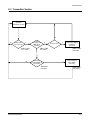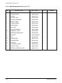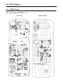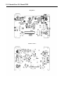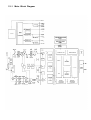
1
PORTABLE CELLULAR
TELEPHONE
SCH-1500 Series
SERVICE
PORTABLE CELLULAR TELEPHONE
Manual
CONTENTS
1. General Introduction
2. Specification
3. Installation
4. Nam Programming
5. Product Support Tools
6. Circuit Description
7. Test Procedure
TALK
END/
1
2 ABC
3 DEF
4 GHI
5 JKL
6 MNO
7PQRS
8 TUV
9WXYZ
OK
9. Exploded Views and Parts List
10. PCB Diagrams
0 OPER
CLR
8. Trouble Shooting
MENU
11. Electrical Parts List
12. Block & Circuit Diagrams
ELECTRONICS
Samsung Electronics Co.,Ltd.
1. General Introduction
The SCH-1500 DBDM phone functions as both analog phone working in AMPS (Advanced Mobile Phone
Service) mode and digital phone working in PCS (Personal Communication Service) mode.
The following standards and minimum performance standards shall be met or exceeded by each subscriber
unit.
Air Interface
The Subscriber Unit shall be Dual mode and Dual band in compliance with ANSI J-STD-008 and TIA/EIA IS95A(Analog).
ANSI J-STD-008 : Personal Station-Base Station Compatibility Requirements for 1.8 to 2.0 GHz CDMA PCS.
ANSI J-STD-018 : Recommended Minimum Performance Requirements for 1.8 to 2.0 GHz CDMA Personal
Stations.
CDG Ref. Document #27 : High Rate Speech Service Option for Wideband Spread Spectrum System.
TIA/EIA IS-96A : Speech Service Option 1 Standard for Dual mode Wideband Spread Spectrum Cellular
Systems.
TIA/EIA IS-125 : Recommended Minimum Performance standards for Digital Cellular Wideband Spread
Spectrum Speech Service Option1.
TIA/EIA IS-126-A : Mobile Station Loop back Service Option standard.
CDMA Receiver/Transmitter Specifications and Requirements
The Subscriber Unit shall comply with ANSI J-STD-008 and meet or exceed TIA/EIA IS-98A. The Subscriber
Unit shall comply with Personal Station Class II.
Analog Receiver/Transmitter Specifications and Requirements
The Subscriber Unit shall comply with TIA/EIA IS-95A and meet or exceed TIA/EIA IS-95. The Subscriber Unit
shall comply with Mobile Station Power Class III (600mW).
Samsung Electronics
1-1
General Introduction
Memo
1-2
Samsung Electronics
2. Specification
2-1 General
Frequency Range
Transmitter
Receiver
PCS Mode
: 1850 ~ 1910 MHz
: 1930 ~ 1990 MHz
AMPS Mode
824 ~ 849 MHz
869 ~ 894 MHz
Channel Spacing
: 1.25 MHz
30 kHz
Number of Channels
: 1200
832
Duplex Spacing
: 80 MHz
45 MHz
Frequency Stability
: (FRX - 80MHz) ± 150Hz
± 2.5 ppm
Operating Temperature
: -30 C ~ 60 C
Operating Voltage
HHP
Hands-free
: 7.2V DC (± 10%)
: 13.7V DC (± 10%)
Size and Weight
including standard battery
including extended-life battery
: 14.6 x 5.4 x 2.5 cm, 191 cc, 220 g (7.7 ounces)
: 14.6 x 5.4 x 3.35 cm, 250 cc, 226 g (7.9 ounces)
Samsung Electronics
o
o
2-1
Specification
2-2 AMPS Mode
TRANSMITTER
RF output power
: 0.6 W (+2/ - 4 dB)
Carrier ON/OFF Conditions
ÒONÓ Condition
ÒOFFÓ Condition
: within ± 3 dB of specification output (in 2mS)
: below - 60 dBm (in 2mS)
Compressor
Compression Rate
Attack Time
Recovery Time
Reference Input
: 2:1
: 3 mS
: 13.5 mS
: Input level for producing a nominal ± 2.9 kHz peak
frequency deviation of transmitted carrier
Preamphasis
: 6 dB/OCT within 0.3 ~ 3 kHz
Maximum Frequency Deviation
F3 of G3
Supervisory Audio Tone
Signaling Tone
Wideband Data
: ± 12 kHz (± 10 %)
: ± 2 kHz (± 10 %)
: ± 8 kHz (± 10 %)
: ± 8kHz (± 10 %)
Post Deviation Limiter Filter
3.0 kHz ~ 5.9 kHz
5.9 kHz ~ 6.1 kHz
6.1 kHz ~ 15 kHz
Over 15 kHz
: above 40LOG (F/3000) dB
: above 35 dB
: above 40 LOG (F/3000) dB
: above 28 dB
Spectrum Noise Suppression
For All Modulation
f0 + 20 kHz ~ f0 + 45 kHz
: above 26 dB
For Modulation by Voice and SAT
f0 + 45 kHz
: above 63 + 10LOG (Py) dB
For Modulation by WBD (without SAT) and ST (with SAT)
f0 + 45 kHz ~ f0 + 60 kHz
: above 45 dB
f0 + 60 kHz ~ f0 + 90 kHz
: above 65 dB
f0 + 90 kHz ~ 2f0
: above 63 + 10LOG (Py) dB
(where f0 = carrier frequency,
Py = mean output power in watts)
Harmonic and Conducted Spurious Emissions
2-2
: above 43 + 10 LOG (Py) dB
Samsung Electronics
Specification
RECEIVER
DE-Emphasis
: -6 dB/OCT within 0.3 ~ 3 kHz
Expander
Expansion Rate
Attack Time
Recovery Time
Reference Input
: 1:2
: within 3 mS
: within 13.5 mS
: Output level to a 1000 Hz tone from a carrier within ±
2.9 kHz peak frequency deviation
Sensitivity
: 12 dB SINAD/-116 dBm
Intermodulation Spurious Response Attenuation
: above 65 dB
RSSI Range
: above 60 dB
Protection Against Spurious Response Interference
: above 60 dB
In Band Conducted Spurious Emissions
Transmit Band
Receive Band
: below -60 dBm
: below -80 dBm
Out of Band Conducted Spurious Emissions
: below - 47 dBm
Radiated Spurious Emissions
Frequency Range
25 ~ 70 MHz
70 ~ 130 MHz
130 ~ 174 MHz
174 ~ 260 MHz
260 ~ 470 MHz
470 ~ 1 GHz
Samsung Electronics
Maximum Allowable EIRP
-45
-41
-41
-32
-32
-21
dBm
dBm
~ -32 dBm
dBm
~ -26 dBm
dBm
2-3
Specification
2-3 PCS Mode
TRANSMITTER
Waveform Quality
: 0.944 or more
Open loop Power Control Range
-25 dBm
-65 dBm
-104 dBm
: -60.5 dBm ~ 41.5 dBm
: -20.5 dBm ~ -1.5 dBm
: +15.0 dBm ~ +30.0 dBm
Minimum Tx Power Control
: -50 dBm below
Closed Loop Power Control Range
: ±24 dB
Maximum RF Output Power
: 200 mW (+23 dBm)
Occupied Bandwidth
: 1.23 MHz
Conducted Spurious Emissions @ 1.25 MHz
: -42 dBc/30 KHz
RECEIVER
Rx Sensitivity and Dynamic Range
(Rate Set 1)
: -104 dBm, FER=0.5% or less
: -25 dBm, FER=0.5% or less
Conducted Spurious Emission
1930 ~ 1990 MHz
1850 ~ 1910 MHz
All Other Frequencies
: <-81 dBm
: <-61 dBm
: <-47 dBm
Single Tone Desensitization
Rx power = -101 dBm
Tone power = -30 dBm
Tone offset from carrier = ±1.25 MHz
: lower than 1%
Intermodulation Spurious Response Attenuation
Rx power = -101 dBm
Tone power 1 = -43 dBm
Tone power 2 = -43 dBm
Tone 1 offset from carrier = ±1.25 MHz
Tone 2 offset from carrier = ±2.05 MHz
: lower than 1%
2-4
Samsung Electronics
Specification
2-4 PCS Debug Display Information
To select debug display mode : Press [MENU] + [8] + [0], and press [0] + [4] + [0] + [7] + [9] + [3] or
press [0] + [0] + [0] + [0] + [0] + [0].
1 Sxxxxx : SID (System Identification) toggle
Nxxxxx : NID (Network Identification) toggle
IN IDLE MODE
1
4
7
2
3
SIDxxxxx SIx
x
T - xx
Dxxx - xx
Pxxx
CHxxxx
xx xx
12
6
8
3 Handset Status : 0 - NO SVC
1 - Synchronization
2 - Paging (Idle)
3 - Reg. Access state
4 - Traffic Initialization
5 - Waiting for order
6 - Waiting for answer
7 - Conversation state
8 - Exit
5
IN CONVERSATION MODE
9
10
2 SIx : Slot cycle index (lowest between the system
and the phone will be used)
1. SI0 : Slot Index 0
2. SI1 : Slot Index 1
3. SI2 : Slot Index 2
11
4 T-xx : Tx adjust, Value ranges from +63~0~63dB
TVx RVx xx x
T - xx
Dxxx - xx
Pxxx
CHxxxx
xx xx
3
5 Dxxx : Sector power in dBm
6 -xx : ec/lo
7 Pxxx : PN offset
12
8 CHxxxx : Channel number
9 TV : Tx vocoder rate (8 is full rate, 1 is 1/8th rate)
10 RV : Rx vocoder rate (8 is full rate, 1 is 1/8th rate)
11 xx : Walsh code used in traffic channel
12 System acquisition state
Samsung Electronics
2-5
Specification
2-5 AMPS Debug Display Information
To select debug display mode : Press [MENU] + [8] + [0], and press [0] + [4] + [0] + [7] + [9] + [3] or
press [0] + [0] + [0] + [0] + [0] + [0].
1 SIDxxxxx : AMPS Home System ID
1
7
4
2 PWRx : Power Level 0 ~ 7
3 SATx : Supervisory Audio Tone code (0 ~ 3)
2
3
SIDxxxxx
x
x
PWRx
RSSIxxx
SATx
CHxxxx
xx xx
5
4 x (Using Frequency Band) : A Band or B Band
5 RSSIxxx : RSSI value
6 CHxxx : Using Channel
8
6
7 Handset Status : 1 - Initialization state
2 - Idle state
3 - System Access state
4 - Voice channel state
8 System acquisition state
2-6
Samsung Electronics
3. Installation
3-1 Installing a Battery Pack
1.
2.
To attach the battery pack after charging, align it
with the phone about 1cm (1/2Ó) away from its
place so that the two arrows on the phone are
seen, the battery charge contacts pointing
downward.
3.
To remove the battery pack, release it by
pressing the button on the rear of the phone.
4.
Slide the battery pack downward about 1cm
(1/2Ó) and lift it away from the phone.
Slide the battery pack upwards until it clicks
firmly into position. The phone is now ready to
be turned on.
Press this button to release
the battery pack.
3-2 For Desk Top Use
1.
Choose a proper location to install the charger
for desk top use.
2.
Plug the power cord of the charger into an
appropriate wall socket. When the power is
connected correctly, the lamps turn on briefly.
3.
To charge the battery pack, insert the battery
pack into the rear slot of the charger. The lamp
marked BAT on the front panel of the charger
lights up red.
4.
If you do not wish to use the phone while
charging the battery, insert the phone with the
battery pack attached into the front slot of the
charger. The lamp marked PHONE on the front
panel of the charger lights up red.
Specifications using DTC
SCH-1500 MAIN
STANDARD
BATTERY
PACK : BTL859S
EXTENDED
BATTERY PACK
: BTL1359L
Battery Type
Charging Time
SEC. code
Standard Battery Extended battery
(Li-Ion, 850mAH)
(Li-Ion, 1350mAH)
3 hours
5 hours
GH43-10114A
GH43-10113A
DTC : DTC59
Figure 3-1 Charging the Phone and Battery
Samsung Electronics
3-1
Installation
3-3 For Mobile Mount
3-3-1 Antenna
3-3-2 Cradle
1.
1.
Choose a location where it is easy to reach and
does not interfere with the driverÕs safe
operation of the car.
2.
Separate the two halves of the clamshell by
removing the two large slotted screws. See the
figure 3-2.
3.
Drill holes and mount the lower half of the
clamshell by using the screws.
4.
Place the cradle onto the remaining half of the
clamshell and assemble them by using the
screws.
5.
Reassemble the two halves of the clamshell
together. Adjust the mounting angle and tighten
the two slotted screws.
Choose a proper location to install the antenna.
¥The center of the roof top provides the best
performance.
¥The edge of the rear trunk also provides a
good performance. However, the antenna
should be higher than the roof of the car.
¥In case of on-glass antenna, you should align
the antenna base with the round plate to
connect the cables correctly.
2.
Mount the antenna vertically, connect the
antenna cable.
3.
Tighten the antenna nut fully.
CRADLE
HHP
ANTENNA
CLAM SHELL
MOUNT UPPER
HANDS
FREE BOX
FIXED SCREW
CLAM SHELL
MOUNT LOWER
CAR
56
40
Figure 3-2 Cradle Installation
3-2
Samsung Electronics
Installation
3-3-3 Hands-Free Box
3-3-4 Hands-Free Microphone
1.
Drill holes in a proper location for the handsfree box, attach the mounting bracket by using
the screws. See the figure 3-3.
1.
2.
Install the hands-free box into the bracket.
It is recommended to install the microphone
where it is 30-45 cm (12-18Ó) away from the
driver. Choose the location where is least
susceptible to interference caused by external
noise sources, ie, adjacent windows, radio
speakers, etc. Normal place is the sun visor.
2.
Once the microphone has been correctly
positioned, connect the microphone wire to the
MIC jack on the hands-free box.
MOUNTING BRACKET
56
40
Figure 3-3 Hands-Free Box Installation
Samsung Electronics
3-3
Installation
3-3-5 Cables
1.
Connect the cradle and the hands-free box with
the data cable. See the figure 3-4.
2.
Connect the antenna cable to the RF jack of the
cradle.
3.
Connect one of the power cable to the battery or
ignition terminal. Connect the red wire to the
battery (+) terminal, black wire to the vehicle
chassis. Then connect the battery (-) terminal to
the vehicle chassis.
4.
Connect the other end of the power cable to the
PWR jack of the hands-free box.
Notes:
¥It is recommended to connect the power cable
directly to the battery to avoid power noise.
¥Make sure the connection between the battery (-)
terminal and vehicle chassis is made correctly.
¥Make sure the fuse having a proper capacity is
used on the power cable.
¥Make sure the cables do not pass over any sharp
metal edge that may damage it.
TA
LK
1
4G
RS
PQ
*
8T
L
9
ER
OP
R
6M
3D
D/
EF
NO
Z
XY
W
#
OK
EN
BC
5 JK
UV
0
CL
2A
HI
7
ME
NU
Figure 3-4 Cable Connections
3-4
Samsung Electronics
4. NAM Programming
NAM features can be programmed as follows:
Notes:
- If you enter the NAM program mode, each item shows the currently stored data. Go to the next item by
pressing OK.
- You can modify the data by entering a new data.
- If you enter a wrong digit, press CLR to delete the last digit. Press and hold CLR to delete all digit.
- To scroll items backwards press the VOLUME button on the left side of the phone.
4-1 Single NAM
4-1-1 General Setup
LCD Display
Key in
Function
Menu, 5, 0
Select NAM programming
Enter Lock
??????
6-digit code
Enter random 6 digit code (MSL)
SVC Menum i
1:Phone#
2:General
3:NAM
2
Choose ÔGENERALÕ
ESN
Volume ¹
Electronic Serial Number of the phone is displayed
CAI version
1
Volume ¹
Common Air Interface version is displayed
SCM
Volume ¹
Station Class Mark displays the power class, transmission,
slotted class, dual mode.
B0000000
10101010
Lock Code
0000
Slot Mode
No
4-digit code
OK
Lock code, current status is displayed.
-to change, enter new code.
-stores it.
m or i
OK
Slot mode. ÔYesÕ indicates the slot mode.
-changes the status.
-store it.
0~7
OK
Slot mode index. The higher, the longer sleeping time.
-to change, enter new one.
-stores it.
Slot Index
2
Samsung Electronics
4-1
NAM Programming
4-1-2 Phone #
LCD Display
Key in
Function
SVC Menum i
1:Phone#
2:General
3:NAM
1
Choose ÔPhone#Õ
Phone #
1234567890
Mobile ID #
1234567890
Phone number
OK
Mobile ID
OK
4-1-3 Setting Up NAM
LCD Display
Key in
Function
SVC Menum i
1:Phone#
2:General
3:NAM
Volume ¹
NAM Programming Menu is displayed.
SVC Menum i
3:NAM
3
Choose ÔSetup NAMÕ.
Number
OK
IMSI Mobile Country Code, current code is displayed.
-to change, enter new one.
-stores it.
Number
OK
IMSI Mobile Network Code, current code is displayed.
-to change, enter new one.
-stores it.
Class number
OK
CDMA Access Overload Class, current status is displayed.
-to change, enter new one.
-stores it.
IMSI_MCC
310
IMSI_MNC
00
CDMA ACCOLC
0
4-2
Samsung Electronics
NAM Programming
LCD Display
Key in
Function
m or i
OK
CDMA Home system ID, current status is displayed
-changes the status
-stores it.
Yes
m or i
OK
CDMA foreign SID, current status is displayed.
-changes the system.
-stores it.
Yes
m or i
OK
CDMA foreign NID, current status is displayed.
-changes the system
-stores it.
Number
OK
SID written in the list, current status is displayed.
-to change, enter new one.
-store it.
Number
OK
NID written in the list, current status is displayed.
-to change, enter new one.
-stores it.
CDMA Home SID
Yes
CDMA fSID
CDMA fNID
HOME SID
1700
NID
1
Samsung Electronics
4-3
NAM Programming
4-2 Dual NAM
4-2-1 General Setup
LCD Display
Enter Lock
??????
SVC Menum i
1:Phone#
2:General
3:NAM1
4:NAM2
ESN
Key in
Function
Menu, 5, 0
Select NAM programming
6-digit code
Enter random 6 digit code (MSL)
2
Choose ÔGENERALÕ
Volume ¹
Electronic Serial Number of the phone is displayed
Volume ¹
Common Air Interface version is displayed
Volume ¹
Station Class Mark displays the power class, transmission,
slotted class, dual mode.
B0000000
CAI version
1
SCM
10101010
Lock Code
0000
Slot Mode
No
4-digit code
OK
Lock code, current status is displayed.
-to change, enter new code.
-stores it.
m or i
OK
Slot mode. ÔYesÕ indicates the slot mode.
-changes the status.
-store it.
0~7
OK
Slot mode index. The higher, the longer sleeping time.
-to change, enter new one.
-stores it.
Slot Index
2
4-4
Samsung Electronics
NAM Programming
4-2-2 Phone # NAM1
LCD Display
Key in
Function
SVC Menum i
1:Phone#
2:General
3:NAM1
4:NAM2
1
Choose ÔPhone#Õ
Phone #
1:NAM1
2:NAM2
1
Choose ÔNAM1Õ
Phone #
1234567890
Mobile ID #
1234567890
Phone number
OK
Mobile ID
OK
4-2-3 Phone # NAM2
LCD Display
Key in
Function
SVC Menum i
1:Phone#
2:General
3:NAM1
4:NAM2
1
Choose ÔPhone#Õ.
Phone #
1:NAM1
2:NAM2
2
Choose ÔNAM2Õ.
Phone #
1234567890
Mobile ID #
1234567890
Samsung Electronics
Phone number
OK
Mobile ID
OK
4-5
NAM Programming
4-2-4 Setting Up NAM1
LCD Display
Key in
Function
SVC Menum i
1:Phone#
2:General
3:NAM1
4:NAM2
Volume ¹
NAM Programming Menu is displayed.
SVC Menum i
3:NAM1
3
Choose ÔSetup NAM1Õ.
Number
OK
IMSI Mobile Country Code, current code is displayed.
-to change, enter new one.
-stores it.
Number
OK
IMSI Mobile Network Code, current code is displayed.
-to change, enter new one.
-stores it.
Class number
OK
CDMA Access Overload Class, current status is displayed.
-to change, enter new one.
-stores it.
m or i
OK
CDMA Home system ID, current status is displayed
-changes the status
-stores it.
Yes
m or i
OK
CDMA foreign SID, current status is displayed.
-changes the system.
-stores it.
Yes
m or i
OK
CDMA foreign NID, current status is displayed.
-changes the system
-stores it.
Number
OK
SID written in the list, current status is displayed.
-to change, enter new one.
-store it.
Number
OK
NID written in the list, current status is displayed.
-to change, enter new one.
-stores it.
IMSI_MCC
310
IMSI_MNC
00
CDMA ACCOLC
0
CDMA Home SID
Yes
CDMA fSID
CDMA fNID
HOME SID
1700
NID
1
4-6
Samsung Electronics
NAM Programming
4-2-5 Setting Up NAM2
LCD Display
Key in
Function
SVC Menum i
1:Phone#
2:General
3:NAM1
4:NAM2
Volume ¹
NAM Programming Menu is displayed.
SVC Menum i
4: NAM2
4
Choose ÔSetup NAM2Õ.
310
Number
OK
IMSI Mobile Country Code, current code is displayed.
-to change, enter new one.
-stores it.
00
Number
OK
IMSI Mobile Network Code, current code is displayed.
-to change, enter new one.
-stores it.
Class number
OK
CDMA Access Overload Class, current status is displayed.
-to change, enter new one.
-stores it.
m or i
OK
CDMA Home system ID, current status is displayed
-changes the status
-stores it.
Yes
m or i
OK
CDMA foreign SID, current status is displayed.
-changes the system.
-stores it.
Yes
m or i
OK
CDMA foreign NID, current status is displayed.
-changes the system
-stores it.
Number
OK
SID written in the list, current status is displayed.
-to change, enter new one.
-store it.
Number
OK
NID written in the list, current status is displayed.
-to change, enter new one.
-stores it.
IMSI_MCC
IMSI_MNC
CDMA ACCOLC
0
CDMA Home SID
Yes
CDMA fSID
CDMA fNID
HOME SID
1700
NID
1
Samsung Electronics
4-7
NAM Programming
Memo
4-8
Samsung Electronics
5. Product Support Tools
5-1 General
These tools enable you to edit or transfer all the EEPROM data of SCH-1500 DBDM phone.
Equipment Required
Software Installation
¥ IBM compatible PC (above 386, 33MHz, 8MB
RAM, DOS 5.0, 500K of memory free to execute
program, and 1MB of disk space free for software
upgrade.)
1. Insert the PST floppy disk into drive (A:).
¥ SCH-1500 DM cable
3. Copy all files of the drive (A:) to the directory
you made.
¥ SCH-1500 Battery
2. Create an appropriate directory to the drive (C:)
for PST software.
4. Execute PSTxx.EXE to run the PST program.
Connection
Connect the test jig to COM1 port on the PC and
connect the interface cable of the test jig to the
phone.
Note : There are three executable files in the new
directory you made:
PSTxx.EXE: PST program where xx is the PST
version number.
Caution : When you use the PST program with a
notebook PC, you might encounter some problems.
Check your serial port setup in your notebook PC
(see your notebook PC manual).
DonÕt worry about the serial port setup when you
use a desktop PC.
Samsung Electronics
5-1
Product Support Tolls
5-2 Product Support Tool (PST)
The Product Support Tool(PST) offers you the
ability to interface with the SCH-1500 DBDM phone
using a personal computer. You can program the
phone, swap phone data, and download software
upgrades.
Notes :
¥ This software is made to be executed on the MSDOS, not on the DOS mode within Windows95. If
this software is executed on Windows 95 by
mistake, it may work abnormally and damage the
phone especially while downloading. Please
check the mode you are using.
¥ You can transfer EEPROM data one unit at a time.
¥ It is illegal to copy to several units.
EDITING FIELDS
Once you are in a particular screen, you may want
to change a value of any field. A highlighted cursor
can be moved to each editable field by using the
arrow keys. A field can only be edited if the cursor
is on that field (that is, if the field is highlighted.)
1. Begin the editing process by pressing <Enter>
key.
2. To accept the new value, press <Enter> key. To
about edit mode and return to the old value,
press <Esc> key.
3. The value of some field that is fixed types will be
changed by just pressing <Enter> key.
See table 5-1 for the list of editing keys.
5-2-1 Getting Started
MAIN MENU SCREEN
5-2-2 Operation Procedure
1. At the DOS prompt, type ÒPSTxxÓ where xx is
the release version.
2. The Main Menu screen is displayed.
SERVICE PROGRAMMING
Notes :
¥ The Main Menu screen shows the basic tasks that
are available.
¥ Move the cursor through the menu choices and
press <Enter> key to select a task.
EXITING THE PROGRAM
1. Press <Esc> key until you find the Main Menu
screen.
2. Select the ÒQUITÓ option on the Main Menu or
press <Alt-X> key, and the PST program is over.
The Service Programming screens enable you to set
and change the service parameters of the phones,
read and write to internal phone book, and transfer
phone book data to other phone. There five options
listed on the Service Programming Main Menu.
The parameter modification is done on the ÒEdit
ParametersÓ screens. The variables found on those
screens can be preset from a phone or a previously
saved file. Select ÒRead Data from FileÓ or ÒRead
Data from PhoneÓ to preset the values.
READ DATA FROM FILE
Use this command to enter the name of a file whose
extension is ÒmmcÓ. The values read from the
named file will initialize the parameter values seen
on the ÒEdit Parameters.Ó
5-2
Samsung Electronics
Product Support Tolls
READ DATA FROM PHONE
SAVE DATA TO FILE
Use this command to replace the current
programmable parameter values with the values
that are currently programmed into the phone.
The values are read from the phone that must be
properly connected to the PST with power on.
Use this command to save the current parameters in
a file. Once you enter a filename, press <Enter> key
to write all current parameters to the file.
WRITE ALL TO PHONE
EDIT PARAMETERS
Use this command to edit Number Assignment
Module (NAM) items and User Preference (U1)
items
There are five screens.
1. General Settings: some writable, some read only.
2. Parameters associated with NAM 1.
3. Parameters associated with NAM 2.
4. First User Preferences.
5. Second User Preferences.
Use this command to write the changed parameter
values to the phone.
Writing the changed values to the phone may take
up to a minute.
Notes :
¥ Some items have dependencies on other items,
and they will be written to the phone together.
¥ If you intend to use this ÒWrite All to PhoneÓ
feature, it is recommended that you do a ÒRead
Data from PhoneÓ first, and then make the
changes, so that nothing gets inadvertently
overwritten.
Function Keys
Esc : Save and Exit
F1 : Displays help message about a selected field.
F6 : Takes you to the General parameters screen.
F7 : Takes you to the NAM 1 parameters screen.
F8 : Takes you to the NAM 2 parameters screen.
F9 : Takes you to the first UI preferences.
F10 : Takes you to the second UI preferences.
Valid & Invalid Data
Upon startup, all items are initialized ÒinvalidÓ.
All fields display the question marks instead of
data. After reading from a phone or a file, if the
question marks still show in a field, then that item
has never been written to the phone or saved to the
file.
Samsung Electronics
5-3
Product Support Tolls
SOFTWARE DOWNLOADER
SETUP
Use this screen to download new software to the
phone. The various windows are displayed to
inform the user of the phone data and the progress
of download.
You can setup SCH-1500 only. Use this screen to
choose com.port. you want to setup.
The software downloader task of the PST is
responsible for downloading a BIN file into the
flash memory on the phone. It verifies that the
given BIN file is compatible with the target phone,
and performs all the protocol necessary to
successfully download the file.
SPACE : Scroll through menu.
Function keys
ENTER : Accepts the phone type chosen.
ESC and ALT-x : Cancel operation and returns to
Main Menu.
To begin a software downloader, use the following
procedure.
QUIT
1. Press <F4> key to choose a BIN file of the new
software to be loaded into the phone. An Edit
box will pop up asking for BIN file name. Enter
full file name or press <Enter> key to see the
lists of BIN files in the current directory. Using
the arrow key, choose the appropriate BIN file,
then press <Enter> key.
You can exit the PST program.
2. Press <F8> key to change the mode of the phone
from hands-free mode to DM offline mode. This
function is to view the software and hardware
version of the phone. By setting the phone to
DM offline mode, the upper left window should
display the phone's data. If the phone fails to
change mode, an error sound and message will
occur. In that case, please check the power, link,
and COM port configuration.
3. Press <ALT-D> key to begin download. Various
messages and progress bar will inform the user
of the progress of the download.
Caution : DO NOT REMOVE POWER WHILE THE
PHONE IS BEING DOWNLOADED !
4. Press <Esc> key to return to Main Menu.
5-4
Samsung Electronics
6. Circuit Description
6-1 Logic Section
6-1-1 Power Supply
CPU
With the battery installed on the phone and by
pressing the PWR key, the VBATT and ON_SW
signals will be connected. This will turn on Q110
(2SC4081BR) and will drive DC-DC converter
(U130) to output 5.2V. This in turn will be supplied
to regulators (U110 and U120), thus releasing them
from the shut-down state to output regulated 3.3V.
INTEL 80186 CMOS type 16-bit microprocessor is
used for the main processing. The CPU controls all
the circuitry. For the CPU clock, 27MHz resonator is
used.
FLASH ROM (U106)
The VBATT applied to ON_SW will turn on Q111
(DTC144EE) resulting in the signal ON_SW_SENSE
to change state from HIGH to LOW. This will allow
MSM to send out PS_HOLD (logical HIGH) to turn
on Q110 even after the PWR key is released.
The voltage (+3.3VD) from U120 is used in the
digital parts of MSM and BBA. The voltage
(+3.3VA) from U110 is used in the analog part of
BBA and Audio circuit.
One 8 MBIT FROM is used to store the terminal's
program. Using the down-loading program, the
program can be changed even after the terminal is
fully assembled.
SRAM (U107)
One 2 MBIT SRAM is used to store the internal flag
information, call processing data, and timer data.
6-1-2 Logic Part
EEPROM (U108)
The Logic part consists of internal CPU of MSM,
RAM, ROM and EEPROM. The MSM receives
TCXO and CHIPX8 clock signals from the BBA and
controls the phone during the CDMA and the FM
mode. The major components are as follows:
¥CPU : INTEL 80186 core
¥FROM
: U126 (MBM29LV800T) - 8MBIT
FLASH ROM
¥SRAM
: U127 (KM68U2000LTGI) - 2MBIT
STATIC RAM
¥EEPROM
: U113 (AT24C128W) - 128KBIT
SERIAL EEPROM
One 128 KBIT EEPROM is used to store ESN, NAM,
power level, volume level, and telephone number.
KEYPAD
For key recognition, key matrix is setup using
SCAN0-6 of STORE signals and KEY0-3 of input
ports of MSM. Eight LEDs and backlight circuitry
are included in the keypad for easy operation in the
dark.
LCD MODULE
LCD module contains a controller which will
display the information onto the LCD by 8-bit data
from the MSM. It also consists a DC-DC converter
to supply -3.5V for fine view angle and LCD
reflector to improve the display efficiency.
Samsung Electronics
6-1
Circuit Description
6-1-3 Baseband Part
MOBILE SYSTEM MODEM (MSM)
ADC Interface
The MSM equipped with the INTEL 80186 CPU
core is an important component of the CDMA
cellular phone. The MSM comes in a 176 pins TQFP
package. The interface block diagram is shown on
page 6-3.
ADC_CLK (pin 3), ADC_ENABLE (pin 1) and
ADC_DATA (pin 2) are required to control the
internal ADC in the BBA.
MICROPROCESSOR INTERFACE
Includes the UART. Also, supports Diagnostic
Monitor (DM) and HP equipment interface.
The interface circuitry consists of reset circuit,
address bus (A0-A19), data bus (AD0-AD15), and
memory controls (ALE, DT_R, HWR/, LWR/,
RAM_CS/, ROM_CS).
CODEC Interface
INPUT CLOCK
¥CPU clock: 27 MHz
¥TXCO/4 (pin 34): 4.92 MHz. This clock signal from
the BBA is the reference clock for the MSM except
in CDMA mode.
¥CHIPX8 : 9.8304 MHz. The reference clock used
during the CDMA mode.
BBA INTERFACE
CDMA, FM Data Interface
¥TXIQDATA0-7 (pins 24-32) : TX data bus used
during both CDMA and FM mode.
¥C_RX_IDATA0-3 (pins 16-20) and C_RX_QDATA03 (pins 12-15) : RX data bus used during CDMA
mode.
¥FM_RX_IDATA (pin 7) and FM_RX_QDATA (pin
8) : RX data bus used during FM mode.
Clock
¥TX_CLK (pin 22), TX_CLK/(pin 23) : Analog to
Digital Converter (ADC) reference clock used in
TX mode.
¥CHIPX8 : ADC reference clock used in CDMA RX
mode.
¥FMCLK : Reference clock in FM RX mode.
6-2
Data Port Interface
The MSM outputs 2.048 MHz PCM_CLK (pin 19)
and 8 KHz CODEC_SYNC (pins 16,20) to the
CODEC (U310). The voice PCM data from the MSM
(U101) PCM_DIN (pin135) is compressed into 8KHz
by QCELP algorithm in the CDMA mode. In FM
mode, the data is processed by D_FM.
RF Interface
TX : TX_AGC_ADJ (pin 35) port is used to control
the TX power level and PA_ON (pin 44) signal is
used to control the power amplifier.
RX : AGC_REF (pin 36) port is used to control the
RX gain and TRK_LO_ADJ (pin 45) is used to
compensate the TCXO clock.
General Purpose I/O Register Pins
Input/output ports to control external devices.
Power Down Control
When the IDLE/ signal turns LOW, only the TX
sections will be disabled. If both the IDLE/ and
SLEEP/ changes to LOW, all the pins except for the
TXCO is disabled.
Samsung Electronics
Circuit Description
ANTENNA
RF
UNIT
XTAL
PA_ON
SYNTH_LOCK
TRK_LO_ADJ
TX_AGC_ADJ
RX_AGC_ADJ
RF
INTERFACE
80186
MICROPROCESSOR
CORE
RESIN/
RESOUT
LWR/
HWR/
RD/
DT_R/
EXTERNAL
RAM, ROM,
EEPROM,
DISPLAY &
OTHER
PERIPHERALS
PCS6/
RAM_CS/
ROM_CS/
EEPROM_CS/
AD0~AD15
A0~A19
MSM2
IDLE/
SLEEP/
FM/
FIFOED SERIAL
DATA PORT
DP_TX_DATA
DP_RX_DATA
MODE
CONTROL
SUPPORT
KEYSENSE0~4
C_RX_IDATA0~3
C_RX_QDATA0~3
CHIPX8
Q5312
CDMA
BASEBAND
ANALOG 2
(BBA2)
I_OFFSET, Q_OFFSET
TXCLK, TXCLK/
TX_IQDATA0~7
MSM 1. 0 CORE
(CDMA
PROCESSING)
RINGER
RINGER
CDMA
MODE
FM
MODE
FM_RX_IDATA
FM_RX_QDATA
FM_RX_STB
FM_RX_CLK
KEYPAD
GENERAL
PURPOSE
INTERFACE
VOCODER
CORE
PCM_CLK
PCM_SYNC
PCM_DIN
PCM_DOUT
CODEC
DFM
PROCESSING
TXCO/4
ADC_ENABLE
ADC_DATA
ADC_CLK
GENERAL
PURPOSE
ADC
SUPPORT
SPK
AMP
MIC
Figure 6-1 Baseband Block Diagram
Samsung Electronics
6-3
Circuit Description
6-1-4 Audio Part
TX AUDIO PATH
The voice signal output from microphone is filtered
and amplified by the internal OP-AMP and is
converted to PCM data by the CODEC (U310). This
signal is then applied to the MSM (U100)'s internal
vocoder.
RX AUDIO PATH
The PCM data out from the MSM is converted to
audio signal by ADC of CODEC (U310), is then
amplified by the speaker amplifier (U330) to be sent
to the speaker unit.
RX AUDIO PATH
De-Emphasis Circuit
This circuit is 1st LPF featuring -6dB/oct to reduce
signal loss and noise in Rx path.
Expander
The expander features 1:2 level to reduce signal loss
and noise in Rx path. The zero crossing level of the
expander is ±2.9 kHz/dev, attack time is 3 mS, and
release time is 13.5 mS.
Volume Adjust
Volume can be adjusted up to 6 steps for the user to
obtain a proper loudness of received signal.
FM TX PATH
Pre-Emphasis Circuit
The circuit features +6dB/oct to reduce signal loss
and noise in Tx path.
6-1-5 TX WBD, ST, And SAT
These signals are generated from MSM. The
modulation level of TX WBD and ST is
±8kHz/dev, and SAT is ±2kHz/dev.
Compressor
The compressor features 2:1 level to reduce signal
loss and noise in Tx path. The zero crossing level of
the compressor is ±2.9 kHz/dev, attack time is 3 mS,
and release time is 13.5 mS.
Limiter
The limiter performs to cut ±0.53 Vp-p or higher
audio signal level so that the FM frequency
deviation is not over ±12kHz/dev. The function is
used to avoid confusion over phone line. LPF is
used to reduce a specific high frequency of limited
signal.
6-4
6-1-6 Buzzer Driving Circuitry
Buzzer generates alert tone. When the buzzer
receives the timer signal from the MSM, it generates
alert tone. The buzzer level is adjusted by the alert
signal's period generated from the MSM timer.
6-1-7 Key Tone Generator
Ringer signal (pin 49) out from MSM (U100) is
passed through 2 serial LPF consisting of R341,
C342, R340, and C341, amplified at the speaker amp
(U330), and comes out to speaker. In hands-free
mode, the key tone is applied to RX audio line
through the LPF and C338, R335.
Samsung Electronics
Circuit Description
6-2 Receiver (For PCS)
LOW NOISE AMPLIFIER (LNA)
IF SAW BAND PASS FILTER
The low noise amplifier featuring 1.6dB Noise
Figure and 16dB gain amplifier a weak signal
receiver from the base station to obtain the
optimum signal level.
IF SAW BPF (F402) is used for CDMA system
having 1.23MHz wide band and ±630kHz
bandwidth. The filter also climinates spurious
signals generated at the mixer.
DOWN CONVERTER (MIXER)
VOLTAGE CONTROLLED OSCILLATOR
First local signal is applied to this down converter.
The down converter transfers the signal amplified
at the LNA into 210.38 MHz IF signal. 210.38MHz
IF signal is made by subtracting 1960 ±30 MHz RF
signal from 1750 ± 30 MHz first local signal. The
LAN is U401 and down converter is U407.
The VCO (U616) generates the signal having
1750MHz center frequency and ±30MHz deviation
with voltage control. PLL IC (U640) controls this
signal.
PHASE LOCKED LOOP (PLL)
LOCAL BUFFER AMPLIFIER
Buffer (U408) amplifies signal to be applied to the
local input of the down converter (U407) when a
phase is locked between U616 and U640.
Input reference frequency is generated at VCTCXO
(U680) and the divider signal is generated at VCO.
PLL compares the two signals and generates the
desired signal with a preprogrammed counter
which controls voltage.
IF AUTOMATIC AGIN CONTROLLER (AGC)
AMP
VOLTAGE CONTROLLED TEMPERATURE
COMPENSATED CRYSTAL OSCILLATOR
210.38MHz IF signal is applied to IF AGC amplifier.
AGC output level is applied to BBA (Base Band
Analog). The AGC amp (U403) keep the signal at a
constant level by controlling the gain. Dynamic
range is 90dB, up gain +45dB, and down gain
-45dB.
It provides 19.68MHz reference frequency to PLL
(U640) and BBA (U600). A correct frequency turning
is made by the voltage control.
TEMPERATURE TO VOLTAGE CONVERTER
RF BAND PASS FILTER (BPF)
The RF BPF (F401) passes only a specific frequency
(1960±30MHz) from the signal received from the
mobile station. The band width is 60MHz.
The Temperature to Voltage Converter (U691)
detects temperature. It is used to compensate active
component characteristics due to the temperature
difference.
DUPLEXER
Duplexer (F406) controls to transmit through the
antenna only the signals within acceptable Tx
frequency range (1880 ±30MHz). It also matches
LNA (U401) input in receiving part and PA out in
transmitter part with the antenna.
Samsung Electronics
6-5
Circuit Description
6-3 Receiver (For AMPS)
LOW NOISE AMPLIFIER (LNA)
IF SAW BAND PASS FILTER
The low noise amplifier featuring 1.6dB Noise
Figure and 16dB gain amplifier a weak signal
receiver from the base station to obtain the
optimum signal level.
IF SAW BPF (F404) is used for AMPS system having
30kHz channel spacing and ±15kHz bandwidth.
The filter also climinates the spurious signals at the
mixer.
DOWN CONVERTER (MIXER)
VOLTAGE CONTROLLED OSCILLATOR
First local signal is applied to this down converter.
The down converter transfers the signal amplified
at the LNA into 85.38 MHz IF signal. 85.38MHz IF
signal is made by subtracting 881 ±12.5 MHz RF
signal from 966 ± 12.5 MHz first local signal. The
LAN is U404 and down converter is U412.
The VCO (U660) generates the signal having
966MHz center frequency and ±12.5MHz deviation
with voltage control. PLL IC (U640) controls this
signal.
PHASE LOCKED LOOP (PLL)
LOCAL BUFFER AMPLIFIER
Buffer (U411) amplifies signal to be applied to the
local input of the down converter (U412) when a
phase is locked between U660 and U640.
Input reference frequency is generated at VCTCXO
(U680) and the divider signal is generated at VCO.
PLL compares the two signals and generates the
desired signal with a preprogrammed counter
which controls voltage.
IF AUTOMATIC AGIN CONTROLLER (AGC)
AMP
VOLTAGE CONTROLLED TEMPERATURE
COMPENSATED CRYSTAL ASCILLATOR
85.38MHz IF signal is applied to IF AGC amplifier.
AGC output level is applied to BBA (Base Band
Analog). The AGC amp (U403) keep the signal at a
constant level by controlling the gain. Dynamic
range is 90dB, up gain +45dB, and down gain
-45dB.
It provides 19.68MHz reference frequency to PLL
(U640) and BBA (U600). A correct frequency turing
is made by the voltage control.
DUPLEXER
RF BAND PASS FILTER (BPF)
The RF BPF (F403) passes only a specific frequency
(881.49±12.5MHz) from the signal received from the
mobile station. The band width is 25MHz.
6-6
Duplexer (F405) controls to transmit through the
antenna only the signals within acceptable Tx
frequency range (836 ±12.5MHz). It also matches
LNA (U404) input in receiving part and PA out in
transmitter part with the antenna.
Samsung Electronics
Circuit Description
6-4 Transmitter Section (For PCS)
POWER AMP
ANTENNA
Power Amp module (U550) amplifier signal to be
sent out to the base station through the antenna.
ANT allows signal to send to receive from the base
station.
DRIVER AMP
RF BAND PASS FILTER (BPF)
The driver amp (U522) allows the signal input to
the Power Amp module (U550) to be within a
specified level.
The RF BPF (F522, F521) accepts only specific
frequency (1880±30MHz) to send it out to power
and Power Amp module. The band width is
60MHz.
UP CONVERTER (MIXER)
ISOLATOR
The up converter (U521) receives the first local
signal to generate 1880±30 MHz from the signal
controlled by TX AGC amp (U501). 1880 ±30 MHz
signal comes out from the mixer output by adding
130MHz IF signal to 1750±30MHz first local signal.
The driver ampÕs reference number is U522 and up
converterÕs reference number is U521.
Isolator (U542) is used to reduce a reflected signal to
protect the power amp module from being
damaged.
POWER SUPPLY REGULATOR
IF AUTOMATIC GAIN CONTROLLER AMP
The signal out to BBA (Base Band Analog) should
be a constant level. The TX IF AGC amp (U501)
controls power to keep the signal at a constant level.
Dynamic range is 85dB, up gain -40dB, and down
gain -45dB.
Samsung Electronics
The power supply regulator (U751, U130) supply a
regulated power to each part of transmitter. U130
supplies 4.8V to Power Amp module (U550). U751
supplies 4.2V to the others.
6-7
Circuit Description
6-5 Transmitter Section (For AMPS)
POWER AMP MODULE
ANTENNA
Power Amp module (U571) amplifier signal to be
sent out to the base station through the antenna.
ANT allows signal to send to receive from the base
station.
UP CONVERTER (MIXER)
RF BAND PASS FILTER (BPF)
The up converter (U561) receives the first local
signal to generate 836±12.5 MHz from the signal
controlled by TX AGC amp (U501). 836 ±12.5 MHz
signal comes out from the mixer output by adding
130MHz IF signal to 966±12.5MHz first local signal.
The RF BPF (F562) accepts only specific frequency
(836±12.5MHz) to send it out to base station
module. The band width is 25MHz.
POWER SUPPLY REGULATOR
IF AUTOMATIC GAIN CONTROLLER AMP
The signal out to BBA (Base Band Analog) should
be a constant level. The TX IF AGC Amp (U501)
controls power to keep the signal at a constant level.
Dynamic range is 85dB, up gain -40dB, and down
gain -45dB.
6-8
The power supply regulator (U751, U130) supply a
regulated power to each part of transmitter. U751
supplies 4.2V to TX driver (U562), mixer (U561) and
TX AGC Amp (U501). U130 supplies 4.8V to power
amp (U571).
Samsung Electronics
Circuit Description
6-6 Desk-Top Rapid Charger
The Desk-Top Rapid Charger DTC58 consists of power supply and controller.
6-6-1 Flyback type SMPS
AC INPUT SECTION
Secondary regulator : Q2, D8, L3, C19
AC power protector and regulator
The rectified dc voltage by D4 and C8 changes to a
constant dc voltage through this circuit.
Alternating line current is converted to a high dc
voltage after being rectified with BD1 and C2. This
circuit also includes AC surge protector MOV1, fuse
F1 to protect circuit from overcurrent, and EMI
noise filter consisting of C1 and LF1.
Inverse voltage protector : D6,D7
This circuit protects voltage leakage from the
battery pack when power is off.
Switching controller and transformer
Switching controller IC1 supplies a constant voltage
and current to the secondary through a photo
coupler IC7. Transformer consists of four coils of
wire wound together. W1 is connected to the
primary, W2 supplies power to IC1, W3 and W4 are
connected to the secondary and supply power. D1
and D2 is a snubber circuit and absorbs a reverse
voltage generated when the transformer's primary
winding is off.
6-6-2 Controller
DC OUTPUT SECTION
It detects battery install, charging status,
output terminal short, and temperature.
MICRO CONTROLLER : HIC
HIC consists of u-COM which controls whole
charging system, and others as follows:
-I/O port
-A/D converter
-Power on delay
-Timer
Constant voltage output : HIC, IC7, VR1
HIC detects the voltage output from secondaries
and feeds back to primary after converting current
using IC7A. The converted current controls IC1
through D3 and IC7B.
BATTERY INSTALL DETECTION : HIC
HIC recognizes that the battery is installed or not by
detecting the voltage between C/F terminal of
battery and GND.
half-wave rectifier : D4, D5, C8, C11
CURRENT DETECTION: R5, R6, R11, R12, HIC
This circuit converts the transformer's alternating
current output to direct current.
The battery charged current is converted to DC by
R5, R6, R11, R12. The voltage is amplified 16 times
through HIC, then applies to u-COM.
Secondary filter : L1, L2, C9, C12
This circuit minimizes the ripple noise in the dc
signal output from the rectifier.
VOLTAGE DETECTION : HIC
HIC pin 12 and 13 detect the input voltage which
applies to u-COM A/D terminal.
Samsung Electronics
6-9
Circuit Description
BATTERY TEMPERATURE DETECTION : HIC,
TH1
HIC calculates the thermistor TH1 resistance value
to determine the battery battery temperature.
CURRENT LIMITER : HIC
It limits current flowing to the battery if the current
is higher than the reference voltage in HIC.
6-7 Travel Charger
Rapid charger, TC59-US is composed of power supply part and control part.
6-7-1 Power Supply Part (Flyback Type Smps Circuit)
AC INPUT SECTION
SECONDARY POWER SECTION
AC input protection circuit and rectifier circuit
Output constant voltage circuit : U4, D24, R17
AC power through the AC plug is rectifiered to DC
power of high voltage through the D1, D2, D3, D4,
C1 and C2. MOV1 is used by protection circuit from
AC power surge. F1 is fuse to prevent overcurrent.
L1 and L2 is EMI noise protection filter of switching
power.
The HIC detects output voltage and compares it
with reference voltage in HIC. The error is fed to
primary circuit by U2B. The feedback error is
converted to current by U2A and D7. The current
controlls U1.
Secondary rectifier circuit : D21, C21
Switching controller and transformer
U1 supplies constant voltage and constant current
to secondary circuit through the transformer. D5, D6
absorbs the reverse voltage when transformer
winding turns off.
The secondary AC output of transformer is rectified
to DC voltage.
Secondary filter circuit : L20, C22
It minimizes the high frequency ripple noise, which
is caused by primary oscilation.
Reverse current protection circuit : D20
When power is off, it protects the reverse flow of
current from battery pack.
6-10
Samsung Electronics
Circuit Description
6-7-2 Control part
MICOM CONTROLLER : U4
VOLTAGE DETECTION CIRCUIT : U4
U4 is include u-COM to controlled whole charging
system and include following internal circuit.
- General input / Output port
- A/D converter
- Reset delay circuit (power on delay)
- Timer
U-COM A/D through U4 pin15 detected voltage.
It is carried following functions
- Battery recognition
- Charging termination condition detection
- Output short detection and output protection
- Temperature detection
Battery temperature detection determined
temperature by use of thermistor resistor variation
of battery by U4.
BATTERY TEMPERATURE DETECTION
CIRCUIT : U4
CURRENT LIMIT CIRCUIT : U4
BATTERY RECOGNITION CIRCUIT : U4
Battery identity detection on determined to voltage
detection battery internal between ID and GND.
When soft-change, current detection circuit limited
current flow to battery, reference voltage mode than
detected current, detected current and U4 internal
reference voltage.
CURRENT DETECTION CIRCUIT : R14, R15,
R16, U4
Battery charging current is changed voltage through
R14, R15, R16. This voltage inputted U-COM to 16
times amplifiered through U4.
Samsung Electronics
6-11
Circuit Description
6-8 Cigarette Lighter Adaptor
6-8-1 Functional Specification
FUNCTIONS OF CLA
SUMMERY
¥ Protection Circuit
Protection Circuit is the circuit against the
electrical stress which is occured at unexpected
conditions of the source power of CLA unit such
as reverse voltage or overcurrent.
This standard describes on the specifications of CLA
(Cigarette Lighter Adapter) for the SCH-1500
DBDM phone of SAMSUNG.
¥ Detection of DBDM phone
If cellular phone is connected to CLA, the CLA
lamp is on to display whether charge will be done
normally or not.
CLA AS ADAPTER AND CHARGER
¥ Adapter
directly supplies power in order to operate DBDM
phone independent of the battery pack.
¥ Detect Carrier-On
In the case of Carrier-On, CLA detects the
resistance of the Cellular Phone and reduces the
charge current.
¥ Charger
for the Li-ion battery pack.
¥ Detect Full-Charge
If the temperature of the battery pack is higher
than the temperature outside of the cellular
phone, CLA detects the battery fully charged and
the state will be converted to the Trickle Charge.
ELECTRICAL SPECIFICATION
¥ Input Voltage : 11V to 30V DC (normal voltage :
13.7V DC)
¥ Output Current
- HHP power & battery power setting : 8.2V DC
±0.05V/ 0mA
- Output current : 0mA to 660mA
- Current limit of this unit should be kept 660mA
± 40mA.
- Output voltage range : 8.2V -0.4/ +0.2
- LED green : 180mA±30mA
¥ Ripple & Noise : 100mVp-p
¥ Normal Fuse Capacity : 250V, 2A
¥ Charging Time
STD : about 4 hours
EXT : about 5 hours
ENVIRONMENTAL SPECIFICATION
CLA CURL CABLE CONNECTION
5
4
3
2
1
PIN NO (CLC)
Description
PIN NO (HHP)
#1
HP power
9
#2
V-BATT
12/13/16
#3
V-F
N.C
#4
C/F
3
#5
GND
2/4/6
¥ Temperature
o
o
- Operating Temperature : -30 C to 75 C
o
o
- Storage Temperature : -35 C to 85 C
¥ Humidity
- Operating Humidity : 5% to 90%
- Storage Humidity : 5% to 95%
6-12
Samsung Electronics
Circuit Description
6-8-2 Circuit description
POWER SUPPLY
CHARGE CURRENT CONTROL CIRCUIT
This circuit supplies HHP& battery with power
received from Cigar Lighter jack of automobile.
U2A, U4, Q1 and side circuit detects R4Õs flowing
current, controls no 5 pin of U1 then charge current
and charge voltage.
POWER CIRCUIT OF CHARGE FOR HHP
POWER & BATTERY
LED ACTIVATING CIRCUIT
This Switching Regulator produces needed power
for charging HHP power & battery, supplied U1,
D1, D2, C1, C2, L1, R25 from Cigar Lighter jack of
automobile.
LED activating circuit compares to voltage
difference between R4 source and D4 PROP controls
Q3, Q4 through U2B comparator for Q6 and side
circuit then activates LED.
CONFIRMING CIRCUIT OF EXITING BATTERY
OR NOT
AUTO POWER ON CIRCUIT
U3A reads separated voltage between resistance
battery C/F and R20, controls no. 5 pin of U1
through reference voltage and comparator then
decides to produce Vcc or not.
Q9, Q10 and side circuit makes power on the circuit
allowed Vcc power to no 9 HHP pin (power on) by
turned on Q9, following up the producing Vcc.
6-9 Hands-Free Kit
6-9-1 Charging Circuit
6-9-3 Speaker circuit
A constant voltage is used for the hands-free kit.
This circuit converts DC 12-24V input current to
8.4V DC to charge the battery. When the battery is
fully charged, the charge current drops and the
circuit operates as a constant voltage.
This circuit eliminates HHP noise, and controls the
sound quality and speaker volume using analog Cmos IC which checks the speaker signal up to 8
steps. 5W audio amplifier amplifies the speaker
signal.
6-9-2 u-Processor
6-9-4 Microphone Circuit
Micro processor controls charging power and
charging current to protect the phone. It also allows
to communicate with a HHP, and to convert from
hands-free mode to private mode, and vice verse. It
adjusts speaker volume at 8 steps and attenuates
echo and noise occurred during conversation.
This circuit separates ground to eliminate the noise
occurring from the HHP antenna and microphone.
u-processor controls this circuit to attenuate echo
which may occur in Land side.
Samsung Electronics
6-13
Circuit Description
6-10 Test Command Table
To change the phone from normal mode to test mode, you should enter the following keys. :
Press [4 7 * 8 6 9 # 1 2 3 5]
Command No.
(OP, AB, RB)
Command SW Name
01(1F, 0, 0)
T_SUSPEND_I
Terminate the normal mode, enter to the test mode.
02(3f, 0, 0)
T_RESTART_I
Terminate the test mode, enter to the normal mode.
03(FD, 0, 0)
T_SAVE_VAL_I
Save value in EEPROM. (Only for Auto test)
04(1D, 0, 1)
T_GET_MODE_I
Get mode. (CDMA or AMPS)
05(1C, 1, 0)
T_SET_MODE I
Set mode to CDMA or AMPS. (Only for Auto test)
06(1E, 0, 0)
T_WRITE_NV_I
Write an EEPROM item. (one of the NV items)
07(81, 0, 0)
T_CARRIERON_I
Turn the carrier on.
08(82, 0, 0)
T_CARRIEROFF_I
Turn the carrier off.
09(83, 4, 0)
T_LOADSYN_I2)
Set the synthesizer to the channel specified by ch_ data.
10(84, 1, 0)
T_PWRLEVEL_I2)
Set the RF power attenuation to the specified value.
11(85, 0, 0)
T_RXMUTE_I
Mute the receive-audio signal.
12(86, 0, 0)
T_RXUNMUTE_I
Unmute the receive-audio signal.
13(87, 0, 0)
T_TXMUTE_I
Mute the transmit-audio signal.
14(88, 0, 0)
T_TXUNMUTE_I
Unmute the transmit-audio signal.
16(8F, 0, 0)
T_STON_I
Transmit a continuous Signaling Tone (ST).
17(90, 0, 0)
T_STOFF_I
Stop transmit a continuous Signaling Tone (ST).
20(94, 4, 0)
T_TEST_SYS_I
22(91,96,96)
Description
Roam Test System
1)
T_SNDNAM_I
Display and send NAM information.
1)
23(95, 3, 4)
T_SNDVERSION_I
24(9F, 7, 8)
T_SNDESN_I
Display and return ESN.
25(92, 0, 0)
T_BACKLIGHT_ON_I
Turn on the backlight.
26(93, 0, 0)
T_BACKLIGHT_OFF_I
Turn off the backlight.
27(96, 0, 0)
T_LAMP_ON_I
Turn on the LAMP.
28(97, 0, 0)
T_LAMP_ON_I
Turn off the LAMP.
29(9A, 5, 0)
T_REBUILD_I
Rebuild EEPROM.
30(9D,16, 0)
T_PLINE_I
Display and return production date.
1)
2)
Display and return S/W version.
32(A0, 1, 0)
T_SATON_I*
Enable the transmission of SAT.
33(A1, 0, 0)
T_SATOFF_I*
Disable the transmission of SAT.
34(A2, 0, 0)
T_CDATA_I
Transmit continuous 5-word Reverse CTL CH message.
35(A3, 0, 0)
T_VOLUME_UP_I
Increase value of the last command. (Only for autotest)
36(A4, 0, 0)
T_VOLUME_DOWN_I
Decrease value of the last command. (Only for autotest)
6-14
Samsung Electronics
Circuit Description
Command No.
(OP, AB, RB)
Signal. Name
Description
2)
42(AA, 1, 0)
T_DTMFON_I
Activate DTMF generator with keycode.
43(AB, 0, 0)
T_DTMFOFF_I
Deactivate DTMF generator.
44(B0, 0, 0)
T_COMPANDORON_I
Enable the compressor and expandor.
45(B1, 0, 0)
T_COMPANDOROFF_I
Disable the compressor and expandor.
46(B2, 0, 0)
T_AMPS_VCLINE_I*
Enter Analog voice channel state.
47(B3, 3, 0)
T_AMPS_AUD_GAIN_I
FM audio gain.
48(B4, 0, 0)
T_VIBRATOR_ON_I
Activate a vibrator.
49(B5, 0, 0)
T_VIBRATOR_OFF_I
Deactivate a vibrator.
50(B6, 0, 4)
T_BATT_TYPE_I
Battery type.
51(B7, 1, 1)
T_BBA_I
BASIC supplier
52(B9, 2, 2)
T_HW_VERSION_I
HW version
57(BC, 0, 0)
T_MIC_ON_I
Mic path on.
58(BD, 0, 0)
T_MIC_OFF_I
Mic path off.
59(BE, 0, 0)
T_ALLPATH_I
Set RX Path, TX path Unmute to Earpiece.
60(BF, 3, 0)
T_AMPS_TX_GAIN_I
61(C0, 3, 0)
T_AMPS_RX_GAIN_I
62(C1, 3, 0)
T_DTMF_VOL_TX_I
63(C2, 3, 0)
T_TX_LIMITER_I
64(C3, 3, 0)
T_AMPS_SAT_LEVEL_I
65(C4, 3, 0)
T_AMPS_FREQ_SGAIN_I
66(C5, 3, 0)
T_AMPS_ST_GAIN_I
2)3)
AMPS TX Audio Gain Control.
2)3)
AMPS RX Audio Gain Control.
2)3)
AMPS TX DTMF Gain Control.
2)3)
AMPS TX Limiter Gain Control.
2)3)
AMPS TX SAT level Control.
2)3)
2)3)
1)
AMPS TX Master Gain Control.
AMPS TX ST Gain Control.
67(C6, 3, 6)
T_READ_BATT_I
68(C8, 0, 3)
T_VBATT1_I
69(C9, 0, 3)
T_VBATT2_I
70(CA, 3, 0)
T_WRITE_BATT_I
71(D1, 3, 0)
T_CDMA_TXADJ_I
72(D2, 3, 0)
T_AMPS_TXADJ_I
73(D3, 1, 0)
T_SET_PA_R_I
Set PA R1, R0 in CDMA.
74(D4, 4, 0)
T_TXRAS_ADJ_I
TX Ras table adjust.
75(D5, 0, 3)
T_READ_RSSI_I
Samsung Electronics
Read low batt in the standby, talk mode.
3)
Set the low battery position in the standby.
3)
Set the low battery position in the talking.
3)3)
2)
2)
2)
3)
Write low battery Level Value to NVM.
Change pdm TX AGC in CDMA.
Change pdm TX AGC in AMPS.
Read a RSSI.
6-15
Circuit Description
Command No.
(OP, AB, RB)
Signal. Name
Description
3)
76(D5, 3, 0)
T_WRITE_RSSI_I
Writes RSSI.
77(D7, 0, 3)
T_READ_TEMP_I
Read Temp.
78(D8, 0, 3)
T_READ_HDET_I
Read High Detect.
79(D9, 1, 0)
T_BUZZER_ON_I
Buzzer On at DTMF 0 key.
80(DA, 0, 0)
T_BUZZER_OFF_I
Buzzer Off.
81(E3, 0, 0)
T_VOC_PCMLPON_I
Play a PCM LOOP BACK.
82(E4, 0, 0)
T_VOC_PCMLPOFF_I
Play off a PCM LOOP BACK.
85(E7, 0, 0)
T_SPEAKER_ON_I
Turn on the speaker path.
86(E8, 0, 0)
T_SPEAKER_OFF_I
Turn off the speaker path.
87(E9, 0, 0)
T_AMPS_LOOP_TEST_I
Play a PCM AMPS loopback.
88(EA, 0, 0)
T_TRK_ADJ_I
RM TRK_LO_ADJ control.
89(EB, 0, 0)
T_CD_TRK_ADJ_I
CDMA TRK _LO_ADJ control.
90(F0, 4, 0)
T_HW_CHANFLAT_I
HW flatness channel.
91(F1, 4, 0)
T_SW_CHANFLAT_I
SW flatness channel.
92(F2, 3, 0)
T_AMPS_TX_PWR_2_I )
93(F3, 3, 0)
T_AMPS_TX_PWR_3_I
Adjust the channel flatness of AMPS.
95(F4, 4, 0)
T_PCS_HW_CHANFLAT_I
PCS HW flatness channel
96(F5, 4, 0)
T_PCS_SW_CHANFLAT_I
PCS SW flatness channel.
97(F6, 4, 0)
T_PCS_CH_CHANFLAT_I
PCS channel flatness adjust.
98(F7, 4, 0)
T_PCS_CH_MAX_MIN_I
Edge channel Max.Min power code.
100(FF, 4, 0)
T_MAX_I
2)
3)
2)3
2)3)
Setting the volume for Power Level.
1) The AB (Input Argument Byte Number) values of these commands are used only in the manual test. In
automatic test mode, the AB is regarded as 0.
2) You can assign the value for these commands. If the AB value is assigned without argument, the test is
achieved with the value stored in EEPROM.
3) After you get a desired test value by performing these commands, if you want to save the value into
EEPROM, use T-SAVE-VAL-I command to store the test value into the corresponding position.
*OP: Operation Command Number
AB: Input Argument Byte Number
RB: Return Byte Number
*SAT 32, 33 are not operating in MSM2 CHIP test
*46 command is required in Rx, and Tx path test at AMPS mode.
6-16
Samsung Electronics
7. Test Procedure
7-1 List of Equipment
¥ DC Power Supply
¥ Test Jig
¥ Test Cable
¥ CDMA Mobile Station Test Set
¥ Spectrum Analyzer (include CDMA test mode)
HP8924C, HP83236B, CMD-80, etc
HP8596E
7-2 Configuration of Test
7-2-1 Hand Set
Spectrum Analyzer
RF In
HP8924C
Test Cable
Duplexer Out
Antenna In
From
Duplexer Out
To ANT In
Directional Coupler
RF In/Out
HP83236B
Test Jig
DC Power Supply
(+7.2 V)
7-2-2 Hands-Free
HANDS FREE
KIT BOX
ANTENNA
CRADLE
DATA
PWR
Orange
Red
Black
Samsung Electronics
DC POWER
SUPPLY
(+13.7V)
7-1
Test Procedure
7-2-3 Test Cable Connection Diagram
TEST JIG
AUTO SELECT
DC POWER INPUT PORT
LEFT: AUDIO IN
RIGHT: AUDIO OFF
CHANGE VOLTAGE LEVEL
BY MODEL (7.2 VDC)
RED: +
BLACK: GND
UP: AUTO POWER ON
DOWN: NOT USE
DB25 CONNECTOR
CONNECT TO DB25
CONNECTOR OF
TEST CABLE
T
E
S
T
AUTO
A-IN
PRB -DC7.2V+
DB9 CONNECTOR
TO PC
CONNECT TO IBM PC
SERIAL PORT
HHP I/F TEST JIG
P
A
C
K
TO HP
TO A-OUT
CONNECT TO
AUDIO OUT PORT OF
TEST EQUIPMENT
(USE BNC CABLE)
TO A-IN
CONNECT TO
AUDIO IN PORT OF
TEST EQUIPMENT
(USE BNC CABLE)
RJ11 CONNECTOR
CONNECT TO HP
SERIAL PORT
PROBE
NOT USED
TEST CABLE
DB25 CONNECTOR
I/F CONNECTOR
CONNECT TO DB25 CONNECTOR OF
TEST CABLE
CONNECT TO HHP
BNC CONNECTOR
CONNECT TO RF IN/OUT PORT OF TEST
EQUIPMENT Cable Loss : 1.2 ~ 2.1 dB
Items needed to purchase from SAMSUNG
ITEMS
PARTS#
REMARK
RF TEST CABLE
GH97-00687A
* Cable Loss : 1.9 GHz (PCS) 2.1 dB, 800 MHz (Cellular) 1.2 dB
RF I/F Pack AssÕy
GH80-10502A
Including
1. Power Cable (Black, Red)
2. 9-pin RS 232 Cable
DM Cable
GH39-30515A
Connection between Phone and PC
7-2
Samsung Electronics
Test Procedure
7-3 Test Procedure
7-3-1 Change the test mode
A. To change the phone from normal mode to test
mode, you should enter the following keys.
: Press [4 7 * 8 6 9 # 1 2 3 5]
B. The command [0 1] (Suspend) is entered to start
test.
: Press [0 1]
C. To finish the test mode, you should enter the
command [0 2]
: Press [0 2]
7-3-2 Channel selection and Tx power
output level control
1.9GHZ (PCS)
A. To select PCS mode, you should enter the
following keys.
1) Press [4 7 * 8 6 9 # 1 2 3 5]
2) Press [2 0 3 0 0 0 0] + [OK] + [0 2]
B. You should change the phone from normal mode
to test mode
: Press [4 7 * 8 6 9 # 1 2 3 5]
C. You should change [0 1] (Suspend) is entered to
start test.
: Press [0 1]
D. You should enter the following keys.
: Press [0 9 0 6 0 0] + [#] + [0 7] + [3 4] +
[7 1 4 0 0]
¥ If you enter the command [0 9] you can select
the channel.
ex) [0 9 X X X X] ; Under bar means channel
number, and channel number must be 4
digits.
¥ The command [0 7] means carrier on.
¥ If you enter the command [3 4] you can
spread the carrier.
Samsung Electronics
¥ If you enter the command [7 1] you can
control the power output level. Following
under bar means AGC code. And you can
control the power output level using
[SEND]/[END/ ] keys.
ex) [7 1 X X X]
¥ [#] key means the escape of current command.
800MHZ CELLULAR (AMPS)
A. To select AMPS mode, you should enter the
following keys.
1) Press [4 7 * 8 6 9 # 1 2 3 5].
2) Press [2 0 1 0 0 0 0] + [OK] + [0 2]
ex) [1 0 0 0 0] means SYS_A, and [1 0 0 0 1]
means SYS_B.
B. You should change the phone from normal mode
to test mode.
: Press [4 7 * 8 6 9 # 1 2 3 5]
C. The command [0 1 4 6 0 1] (Suspend) is entered
to start test.
: Press [0 1] + [4 6] + [0 1]
D. You should enter the following keys.
: Press [0 9 0 3 6 3] + [#] + [0 7] + [7 2 3 6 3]
¥ If you enter the command [0 9] you can select
the channel.
ex) [0 9 X X X X] ; Under bar means channel
number, and channel number must be 4
digits.
¥ The command [0 7] means carrier on.
¥ If you enter the command [7 2] you can
control the power output level. Following
under bar means AGC code. And you can
control the power output level using
[SEND]/[END/ ] keys.
ex) [7 2 X X X]
¥ [#] key means the escape of current command.
7-3
Test Procedure
Memo
7-4
Samsung Electronics
8. Troubleshooting
8-1 Logic Section
8-1-1 No Power
Press PWR button.
U120 pin3,4 input =5.2V?
N
Check U120 and its neighboring circuits
Y
U110 pin6 input = S5.2V?
N
Check U110 and its neighboring circuits.
Y
U120 pin 6 output=3.3V?
N
Check U120 and its neighboring circuits.
Y
U110 pin4 output=3.3V?
N
Check U110 and its neighboring circuits.
Y
END
Samsung Electronics
8-1
Troubleshooting
8-1-2 Abnormal initial operation (Normal +3.3V voltage source)
Press PWR Key
TCXO CLK
applied to U600 pin 26?
N
Check VCTCXO output, C600
Replace if required.
N
Check U600 and its neighboring
circuits. Replace if required.
N
Check MSM board, U100 pins 93-96,
98-105, 107-117, 119-126, and
128-132. Replace if required.
N
Check 'H' level input from
U200 pin59, U600 pin79.
N
Check the LED and its neighboring
circuits. Replace if required.
N
Check the LCD pins and its neighboring
circuits. Replace if required.
Y
TCXO/4 CLK signal outputted
from U600 pin 29?
Y
RAM-CS signal outputted
from U100 pin 92?
Y
CHIP X 8 CLK
signal outputted from
U600 pin 52?
Y
LED on?
Y
Normal initial
display on LCD?
Y
END
8-2
Samsung Electronics
Troubleshooting
8-1-3 Abnormal Backlight Operation
Press any button on the phone.
'H' level outputted
from U100 pin 60?
N
Check U100 pin 60. Replace if required.
Y
'H' level
from U100 pin 60 drive Q140
through R144?
N
Check R142, R144, and Q140.
Replace if required.
N
Check R146, R147, R148 and
Q141. Replace if required.
Y
Normal Q141 operation?
Y
The voltage applied
to LCD pins 38, 41?
N
Resolder R141 and R142.
Y
Backlight LED on
Samsung Electronics
8-3
Troubleshooting
8-1-4 Abnormal Key Data Input
Check initial status.
Scanning signals
outputted from U100 pins159,
160, 163-167?
N
Resolder U100 pins 159, 160
and 163-167.
Y
Resolder U100
pins 168, 169, 170, 172 and 173.
Resolder J100.
Y
Normal Key data input?
N
Replace the Keypad assembly.
Y
END
8-4
Samsung Electronics
Troubleshooting
8-1-5 Abnormal Keytone
Abnormal keytone.
CLK waveform outputted
from U100 pin 49?
N
Check U100 pin 49. Replace if required.
Y
CLK waveform applied
from U330 pin 2?
N
Resolder R341, C342, R340, C341,
C337, and C334
Y
CLK waveform applied
to U330 pin 3?
N
Check U330, C333, and C334.
Replace if required.
Y
Normal keytone?
N
Replace the Keypad assembly.
Y
END
Samsung Electronics
8-5
Troubleshooting
8-1-6 Abnormal Alert Tone
Abnormal Keytone.
'Low' level on U100 pin 56?
N
Check U100 pin 56. Replace if required.
Y
CLK waveform applied
to J100 pin 12?
N
Check Q350, Q351, R350 and D350.
Replace if required.
Y
Is the buzzer
connection correct?
N
Connect the buzzer correctly.
Y
Check the buzzer
and replace if required.
8-6
Samsung Electronics
Troubleshooting
8-2 Receiver Section
8-2-1 AMPS mode
Start AMPS mode.
Check
AMPS 12dB SINAD
OK?
Y
N
Check LNA
in/output OK?
N
Check Duplexer
& LNA power.
(Gain: +16dB)
Y
Y
Check MIXER
in/output OK?
N
Check 1st
N
local & mixer power
OK?
(Gain(AMPS): +10dB)
(Local:0dBm)
Y
Check IF Filter
in/output OK?
N
Check PLL(U640)
& VCO output.
(VCO output: -6dBm)
Check IF Filter
soldering.
(Loss: -5dB)
Y
Y
Check AGC amp
in/output OK?
N
Check 2nd
local & AGC control
vlotage OK?
N
Check PLL(U640)
& BBA #80.
(Gain: +/-45dB)
Y
RF RX AMPS OK.
(BBA input: -53dBm)
Samsung Electronics
8-7
Troubleshooting
8-2-2 PCS mode
Start PCS mode.
Normal PCS SVC
& ROAM OK?
N
Check PCS Rx path.
Y
Setup PCS call. OK?
N
Check Transmitter.
Y
Measure PCS FER.
N
8-8
Normal PCS RF?
Samsung Electronics
Troubleshooting
8-3 Transmitter Section
Abnormal
Transmitter section.
N
N
Check U501
TX IF Level OK?
Y
Check
U521(PCS), U561
(AMPS) RF out
Level OK?
AMPS:-21dBm
PCS:-13dBM
N
Check PLL OK?
Y
AMPS:-17dBm
PCS:-4dBM
Check U563(AMPS)
U524(PCS)
local level.
AMPS:-10dBm
PCS:-3dBm
Y
N
Check U522
(PCS) U562(AMPS) RF
Out level OK?
AMPS:3dBm
PCS:7dBm
Samsung Electronics
Y
Check U550(PCS)
U571(AMPS)
Pout level.
AMPS:28dBm
PCS:23dBm
8-9
Troubleshooting
8-4 Desk-Top Rapid Charger
N
N
Bat. A installed?
Y
Y
Set Bat. A as
Master Mode
Bat. B installed?
Y
Bat. B installed?
Set Bat. B as
Master Mode
N
N
Bat. A installed?
Y
N
Bat. A removed?
N
N
Y
Bat. A
charging finished?
Y
Set Bat. A as
Trickle charge mode
Bat. B
charging finished?
N
Y
Y
Set Bat. B as
Trickle charge mode
N
N
Bat. B removed?
Y
N
Bat. B
charging finished?
Y
Set Bat. B as
Trickle charge mode
8-10
Bat. B removed?
Bat. A
charging finished?
Y
N
Bat. A removed?
Y
Set Bat. A as
Trickle charge mode
Samsung Electronics
Troubleshooting
8-5 Travel Charger
In case of charge fault
(test with 6.2V battery)
Is LED turned on ?
Is Q7 turned on?
1
Change AH1504F
Check R14, 15, 16, U2B, U2A
1
Is Q7 turned on ?
Is charge curent
over 630mA ?
Samsung Electronics
Check F1, L1, AH1504G
Check R14, 15, 16, U2B, U2A
8-11
Troubleshooting
8-6 Cigarette Lighter Adaptor
In the case of LED-on fault
Is battery pack connected ?
N
Connect battery to a phone
Y
Is the value of V/F correct ?
N
Battery pack fault
Y
Is the voltage at
pin-5 of U1 high ?
N
Check F1, U1, U3, Q8, Q7
Y
Check the interface
plug and phone
8-12
Samsung Electronics
Troubleshooting
In the case of charge fault
(test with a battery of 6.2V)
Is the color of LED red ?
N
Check Q6, U2B, Q4, U1
Y
Is the voltage at
R7 under 2.48V ?
N
Check R6, R7, VR1, U4
Y
Is the voltage at
pin-5 of U1 high ?
N
Check F1, U1, U3, Q8, Q7
Y
Check the interface
plug and phone
Samsung Electronics
8-13
Troubleshooting
8-7 Hands Free Kit
8-7-1 Power
N
D1 > 12V
Check Power Cable
Fuse from the
10, 13PIN of CON4
Y
F2 > 12V
N
Y
Check the
voltage between R100
and R101, more
than 12V(?).
N
Ignition(CON4 6PIN)
Call on Signal Check.
Y
Q13, E2 Check
HFPWR > 12V
N
To connect Hand Set.
Check low state
from MGND.
Y
EXPWR > 12V
N
Check low STATE from
R96 and, Check
R19//18//18+//18++//17
(more than 0.3V ?)
Y
END
8-14
Samsung Electronics
Troubleshooting
8-7-2 Audio Part
MIC PIN
Check MIC PIN, Signal OK?
N
Check R29, and CON2 R32
Y
Check U6A(1PIN), Signal OK?
N
Check C12, R34, and 35
Y
Check U6C(8PIN), Signal OK?
N
Check C14, and U7
Y
END
SPEAKER
Y
Check SPEAKER, output OK?
N
Check SPK PIN, Signal OK?
N
Check Cradle, and Cable
Y
Check U8B(7PIN), Signal OK?
N
Check U8, R72, 49, 60, and U10
Y
END
Samsung Electronics
8-15
Troubleshooting
8-7-3 Data Comm & Cont.
Check MPU (1PIN), 5V?
N
Check INTPWR PIN, and U4
Y
Normal X1 output?
N
Check C40, and C41
Y
Check MPU 17, and 18PIN,
DATA PULSE?
N
Check D11, D15, Q11, and 12
Y
END
8-16
Samsung Electronics
9. Exploded Views and Parts List
9-1 DBDM Phone Exploded View
9-2 DBDM Phone Parts List
9-3 Desk-Top Rapid Charger Exploded View
9-4 Desk-Top Rapid Charger Parts List
9-5 Travel Charger
9-6 Cigarette Lighter Adaptor
9-7 Hands Free Kit Exploded View
9-8 Hands Free Kit Parts List
9-9 Cradle Exploded View
9-10 Cradle Parts List
9-11 Main Packing Layout
9-11-1 Main Packing Layout (with DTC)
9-11-2 Main Packing Parts List (with DTC)
9-11-3 Main Packing Layout (with TC)
9-11-4 Main Packing Parts List (with TC)
9-12 Hands-Free Kit Packing Layout
9-13 Hands-Free Kit Packing Parts List
Samsung Electronics
9-1
Exploded Views and Parts List
9-1 DBDM Phone Exploded View
1
2
3
49
53
4
5
6
50
48
7
8
9
11
10
12
15
16
13
17
14
18
51
19
52
21
20
46
55
22
24
25
23
27
54
26
28
29
47
33
30
36
34
31
37
32
38
35
39
40
42
41
43
44
45
9-2
Samsung Electronics
Exploded Views and Parts List
9-2 DBDM Phone Parts List
NO
LEVEL
DESCRIPTION
1
2
SEC. CODE
Q’TY
MEA FRONT ASS’Y
GH97-01297A
1
MEC FRONT ASS’Y
GH75-00032A
1
SCH-1500
GH75-11185A
1
SCH-1510/1530/1531
3
3
TAPE WINDOW
GH74-10657A
1
4
3
FRONTCOVER
GH72-41604A
1
8
3
SPONGE LCD
GH73-10513A
1
12
3
TAPE SPEAKER
GH74-10546A
1
49
3
REFLECT LED
GH72-40008A
1
REMARK
1
2
TAPE WINDOW BOHO
GH72-10001A
1
2
2
WINDOW LCD
GH72-30011A
1
SCH-1500
GH72-30015A
1
SCH-1510
GH72-30017A
1
SCH-1530
GH72-30019A
1
SCH-1531
5
2
SHIELD STRIP(C)
GH71-10641A
1
6
2
SHIELD STRIP(B)
GH71-10640A
1
7
2
KNOB VOLUME
GH64-10017A
1
9
2
KEYPAD RUBBER
GH73-40652A
1
SCH-1500
GH73-40710A
1
SCH-1510/1530/1531
10
2
BUZZER HOLDER
GH73-40709A
1
11
2
CLOTH POLYESTER
0107-001004
1
13
2
SPONGE
GH74-10743A
1
14
2
RUBBER BUZZER
GH73-40649A
1
15
2
BUZZER TAPE
GH74-10742A
1
16
2
KEYPAD PCB ASS’Y
GH59-10072A
1
17
2
HOLDER MIC
GH73-40538A
1
18
2
CLOTH POLYESTER
GH63-20001A
1
19
2
RUBBER BUZZER
GH73-40649A
1
20
2
SHIELD COVER
GH72-41557A
1
48
2
GASKET CLOTH BUZZER
GH63-20001A
1
50
2
SHIELD STRIP(A)
GH71-10639A
1
51
2
SHIELD TAPE
GH74-00100A
2
52
2
SHIELD COVER SPONGE
GH74-00082A
3
53
2
GASKET
GH63-00002A
1
Samsung Electronics
9-3
Exploded Views and Parts List
NO
LEVEL
DESCRIPTION
1
2
SEC. CODE
Q’TY
MEA REAR ASS’Y
GH97-01296A
1
MEC REAR ASS’Y
GH75-11186A
1
35
3
BUSHING ANTENNA
GH71-40004A
1
38
3
REAR COVER
GH72-41559A
1
39
3
SPRING LOCKER
GH70-10516A
1
40
3
LOCKER MAIN
GH72-41560A
1
27
2
SHIELD FRAME
GH71-10003A
1
28
2
SHIELD STRIP(B)
GH71-10640A
1
29
2
SHIELD STRIP(D)
GH71-10643A
1
30
2
SHIELD STRIP
GH71-10644A
1
32
2
SPONGE
GH74-10526A
1
33
2
TAPTITE SCREW (M2.6 X 4)
6003-000366
1
34
2
MOTOR
GH31-10002A
1
47
2
SHIELD STRIP(F)
GH71-00019A
1
54
2
SHIELD STRIP(B)
GH71-10640A
1
REMARK
21
1
SHIELD CAN
GH71-10727A
1
22
1
PBA MAIN-1500 PBA
GH92-01165A
1
23
1
COVER CONNECTOR
GH73-40005A
1
24
1
D-BOARD TAPE
GH74-10723A
1
EXCEPT SCH-1530/1531
25
1
HOLDER PLATE
GH71-10009A
2
EXCEPT SCH-1530/1531
26
1
D-BOARD
GH41-10638A
1
EXCEPT SCH-1530/1531
31
1
SHIELD SPONGE
GH74-10585A
1
EXCEPT SCH-1530/1531
36
1
ANTENNA TUBE
-
1
37
1
ANTENNA
GH42-10521A
1
41
1
BAR CODE LABEL
JF68-30527H
1
42
1
MACHINE BH M2 L8 STAR
6001-000101
4
43
1
LABEL ID MAIN
GH68-31107A
1
SCH-1500
GH68-31166A
1
SCH-1510
GH68-31168A
1
SCH-1530/1531
44
1
STD BATT. ASS’Y
GH43-10114A
1
45
1
LONG BATT. ASS’Y
GH43-10113A
1
46
1
CONTACT SPONGE
GH74-00065A
1
55
1
ANTENNA CONTACT
GH71-10694A
1
9-4
Samsung Electronics
Exploded Views and Parts List
9-3 Desk-Top Rapid Charger Exploded View
Charging Time Standard Battery (850mAH)
3 hours
Extended Battery (1350mAH) 5 hours
Environmental Charge
Specification
0 oC ~ 40 oC
Storage
-30 oC ~ 80 oC
Desk-Top Rapid Charger Ass’y : GH44-40072A
1
6
5
4
3
2
9
7
5
8
10
11
12
13
14
Samsung Electronics
9-5
Exploded Views and Parts List
9-4 Desk-Top Rapid Charger Parts List
NO
9-6
DESCRIPTION
SEC. CODE
Q’TY
1
CASE, TOP
1
2
HOUSING, BATTERY
1
3
HOOK, PLATE (LARGE)
1
4
HOOK (B)
2
5
WASHER
4
6
VH, M2.6, L6 (2W), BLK
4
7
HOOK (A)
2
8
VH, M3, L8, BLK
3
9
ASS’Y, AC POWER CORD
1
10
ASS’Y, R/C BOARD
1
11
CASE, BOTTOM
1
12
BUMPON
4
13
VH, M2.6, L12(2W), BLK
4
14
LABEL, ID, R/C
1
REMARK
Samsung Electronics
Exploded Views and Parts List
9-5 Travel Charger
Travel Charger Ass’y : GH44-40082A
Standard Battery (850mAH)
3 hours
Extended Battery (1350mAH)
6 hours
Environmental
Charge
0 oC ~ 40 oC
Specification
Storage
-30 oC ~ 80 oC
Charging Time
Samsung Electronics
9-7
Exploded Views and Parts List
9-6 Cigarette Lighter Adaptor
Cigatte Lighter Adaptor Ass’y : GH44-40075A
Standard Battery (850mAH)
4 hours
Extended Battery (1350mAH)
5 hours
Environmental
Charge
0 oC ~ 40 oC
Specification
Storage
-30 oC ~ 80 oC
Charging Time
9-8
Samsung Electronics
Exploded Views and Parts List
9-7 Hands Free Kit Exploded View
Hands Free Kit Ass’y : GH96-01103A
2
1
3
4
5
6
8
7
9
10
Samsung Electronics
11
9-9
Exploded Views and Parts List
9-8 Hands Free Kit Parts List
NO
9-10
DESCRIPTION
SEC. CODE
Q’TY
1
HOUSING, UPPER, H/F
GH97-00693A
1
2
LABEL, LOGO, H/F
GA68-30642A
1
3
FELT, SPEAKER, H/F
GH74-10521A
1
4
AUDIO SPEAKER, C/D
3001-000186
1
5
TAPTITE, B, BH, +, M3, L6
6003-000115
4
6
PBA
GH41-1056AA(100)
1
7
HEATSINK, H/F
GH71-10559A
1
8
BUMPON
9
HOUSING, LOWER, H/F
GH97-00694A
1
10
TAPTITE, B, BH, +, M3, L12
6003-000161
4
11
LABEL, ID, HFK
GH68-30841A
1
REMARK
2
Samsung Electronics
Exploded Views and Parts List
9-9 Cradle Exploded View
1
2
3
4
5
7
6
8
9
8
11
12
10
14
16
15
13
Samsung Electronics
9-11
Exploded Views and Parts List
9-10 Cradle Parts List
NO
DESCRIPTION
SEC. CODE
Q’TY
1
HOUSING, UPPER
GH72-40739A
1
2
SOCKET, PLATE
GH70-10526A
1
3
LOCKER
GH72-40742A
2
4
SPRING, TORTION
GH70-10527A
2
5
EJECTOR
GH72-40743A
1
6
SPRING, EJECTOR
GH70-10520A
2
7
FRAME
GH72-40741A
1
8
TAPTITE, B, BH, +, M2.6, L6, C BLK
6003-000107
6
9
PBA, CRADLE
GH41-10573A
1
10
HOUSING, LOWER
GH72-40740A
1
11
TAPTITE, B, BH, +, M2, L6, C BLK
6002-000342
1
12
HOLDER, CRADLE
GH72-40622A
1
13
CURL CORD
GH39-60506A
1
14
MAS, B, BH, +, M3, L8
6001-000133
1
15
LABEL, ID
GH68-30832A
1
16
DATA CABLE
GH81-10504A
1
9-12
REMARK
Samsung Electronics
Exploded Views and Parts List
9-11 Main Packing Layout
9-11-1 Main Packing Layout (with DTC)
7
8
9 10
11 17 18 19
6
WXYZ
9
#
MENU
TUV
8
OK
OPER
0
PQRS
*
7
CLR
12
PWR
END
DEF
2
JKL
5
1
4
GHI
TALK
ABC
6
3
2
MNO
Sprint
1
3
13
15
14
16
4
5
Samsung Electronics
9-13
Exploded Views and Parts List
9-11-2 Main Packing Parts List (with DTC)
NO
DESCRIPTION
SEC. CODE
Q’TY
1
SHIELDING BAG
GH69-30500A
1
2
PE BAG
GG69-30517A
1
3
BAG STD. BATT.
GH69-30503A
1
4
CUSHION CASE MAIN
GH69-20680A
1
5
BOX GIFT MAIN
GH69-11146A
1
6
PP-BAG MANUAL
GH69-30518A
1
7
USER MANUAL
GH68-60671A
1
8
IPR CARD
GH68-60564A
1
9
QUICK REFERENCE
GH68-70688A
1
10
WARRANTY CARD
GH68-70560A
1
11
MAN(BOOK)-INSURANCE
GH68-60564A
1
12
MAIN SET
SCH-1500B/XAR
1
13
DTC
GH44-40072A
1
14
STD BATTERY
GH43-10114A
1
15
HANGER STRAP
GH72-41051A
1
16
SILICAGEL
GA69-90502A
1
17
ACCESSORY GUIDE
GH68-00218A
1
18
ACTIVITY CARD
GH68-70750A
1
19
TERMS & CONDITION CARD
GH68-70751A
1
9-14
REMARK
Samsung Electronics
Exploded Views and Parts List
9-11-3 Main Packing Layout (with TC)
11 12 14 15 16
10
1
13 17 18
2
6
3
9
7
8
4
19
5
Samsung Electronics
9-15
Exploded Views and Parts List
9-11-4 Main Packing Parts List (with TC)
NO
DESCRIPTION
SEC. CODE
Q’TY
REMARK
1
SHIELDING BAG
GH69-30500A
1
2
PE BAG
GG69-30517A
1
SCH-1510
GA69-30533A
1
SCH-1530/1531
3
BAG STD. BATT.
GH69-30503A
1
4
CUSHION CASE MAIN
GH69-20769A
1
5
BOX GIFT MAIN
GH69-11266A
1
SCH-1510
GH69-11268A
1
SCH-1530/1531
SCH-1510B/CDT
1
SCH-1510
SCH-1500BB/XAR
1
SCH-1530/1531
6
MAIN SET
7
TC
GH44-40082A
1
8
STD BATTERY
GH43-10114A
1
9
HANGER STRAP
GH72-41051A
1
10
PP-BAG MANUAL
GH69-30518A
2
SCH-1510 : 1EA
11
IPR CARD
GH68-70752A
1
EXCEPT SCH-1510
12
QUICK REFERENCE (ENGLISH)
GH68-00051A
1
EXCEPT SCH-1510
13
QUICK REFERENCE (FRENCH)
1
EXCEPT SCH-1510
14
WARRANTY CARD
GH68-70737A
1
EXCEPT SCH-1510
15
RESISTRATION CARD
GH68-70735A
1
EXCEPT SCH-1510
16
USER MANUAL (ENGLISH)
GH68-00050A
1
EXCEPT SCH-1510
17
USER MANUAL (FRENCH)
GH68-00052A
1
EXCEPT SCH-1510
18
USER MANUAL
GH68-00244A
1
SCH-1510
19
SILICAGEL
GA69-90502A
1
9-16
GH68-00053A
Samsung Electronics
Exploded Views and Parts List
9-12 Hands-Free Kit Packing Layout
1
2
3
5
4
6
7
8
Samsung Electronics
9-17
Exploded Views and Parts List
9-13 Hands-Free Kit Packing Parts List
NO
DESCRIPTION
SEC. CODE
Q’TY
1
USER’S MANUAL, H/F
GH68-60560A
1
2
ASS’Y, CRADLE
GH90-00578A
1
3
POWER CABLE
GH39-10501A
1
4
ASS’Y, HANDS-FREE MICROPHONE
1
5
CLAMSHELL, MOUNT
1
6
ASS’Y, HANDS-FREE KIT/BRACKET MOUNTING
GH90-00577A
1
7
CUSHION, BASE
GH69-20550A
1
8
BOX, GIFT
GH69-10842A
1
9-18
REMARK
Samsung Electronics
10. PCB Diagrams
10-1
DBDM Phone
10-1-1 Main Board PCB (REV : 2.1)
Top View
Bottom View
10-1-2 Memory Board PCB (REV : 2.0)
10-2 Desk-Top Rapid Charger Board PCB
10-3 Travel Charger Board PCB
10-4 Cigarette Lighter Adaptor Board PCB
10-5 Hands-Free Kit Board PCB
10-6 Cradle PCB
Memo
11. Electrical Parts List
11-1 DBDM Phone
11-1-1 Main Board Assembly
NO
DESCRIPTION
SEC.CODE
REMARK
- Capacitors C100,C101
Ceramic, 18P
2203-000425
C106,C107,C108
Ceramic, 0.1U
2203-000189
C111
Tantalum, Chip 1U/16V
2404-000151
C112
Ceramic, 0.1U
2203-000189
C113
Tantalum, Chip 10UF/6.3V
2404-000139
C114
Ceramic, 1000P
2203-000438
C120
Tantalum, Chip 1U/16V
2404-000151
C121
Ceramic, 0.1U
2203-000189
C122
Tantalum, Chip 10UF/6.3V
2404-000139
CI30
Tantalum, Chip 100U/16V
2404-001003
C131
Ceramic, 0.1U
2203-000189
C132
Ceramic, 3300P
2203-000714
C133
Ceramic, 27P
2203-000679
C134
Tantalum, Chip 220U/10V
2404-001025
C135
Ceramic, 1000P
2203-000438
C136
Ceramic, 100P
2203-000234
C140.C141
Tantalum, Chip 1U/16V
2404-000151
C142
Tantalum, Chip 4.7U/10V
2404-000232
C160
Ceramic, 0.01U
2203-000254
C165,C310
Ceramic, 0.1U
2203-000189
C311,C312,C313
Tantalum, Chip 1U/16V
2404-000151
C314
Ceramic, 1U
2203-005065
C315
Ceramic, 39P
2203-000854
C320
Ceramic, 0.1U
2203-000189
C321
Ceramic, 220P
2203-000585
C323
Ceramic, 1U
2203-005065
C324
OPEN_C
OPEN_C
C325
Ceramic, 0.1U
2203-000189
C326,C327,C328
Ceramic, 15P
2203-000386
C330
Ceramic, 1500P
2203-000138
C331
Ceramic, 5600P
2203-001033
C332
Ceramic, 0.1U
2203-000189
C333,C334
Ceramic, 680P
2203-001124
Samsung Electronics
11-1
Electrical Parts List
NO
DESCRIPTION
SEC.CODE
C335
Tantalum, Chip 4.7U/10V
2404-000232
C336
Ceramic, 2200P
2203-000489
C337
Ceramic, 0.01U
2203-000254
C338
Ceramic, 5600P
2203-001033
C339
Ceramic, 0.01U
2203-000254
C340
Ceramic, 390P
2203-000836
C341
Ceramic, 0.022U
2203-001405
C342
Ceramic, 0.1U
2203-000189
C350,C351,C353,
Ceramic, 15P
2203-000386
C362
Ceramic, 0.033UF
2203-001416
C364
Ceramic, 0.01U
2203-000254
C365
Ceramic, 1000P
2203-000438
C370,C371
Ceramic, 8200P
2203-001210
C375
Ceramic, 0.01U
2203-000254
C376
Ceramic, 0.1U
2203-000189
C377
Ceramic, 0.01U
2203-000254
C378
Ceramic, 0.1U
2203-000189
C379
Tantalum, Chip 1U/16V
2404-000151
C383,C384
Ceramic, 470P
2203-000941
C388
Ceramic, 0.01U
2203-000254
C389
Ceramic, 0.1U
2203-000189
C390
Ceramic, 0.01U
2203-000254
C391
Ceramic, 0.1U
2203-000189
C392
Ceramic, 0.01U
2203-000254
C393
Ceramic, 0.1U
2203-000189
C394
Ceramic, 0.01U
2203-000254
C395
Ceramic, 0.1U
2203-000189
C396
Ceramic, 0.01U
2203-000254
C397
Ceramic, 0.1U
2203-000189
C398
Ceramic, 0.01U
2203-000254
C399
Ceramic, 0.1U
2203-000189
C401
Ceramic, 1000P
2203-000438
C402
Ceramic, 2700P
2203-000530
C403
Ceramic, 4P
2203-001017
C405
Ceramic, 100P
2203-000234
C407
Ceramic, 1000P
2203-000438
C408,C409
Ceramic, 100P
2203-000234
C410
Ceramic, 5P
2203-001437
C411
Ceramic, 3P
2203-000870
REMARK
C354,C355,C356
11-2
Samsung Electronics
Electrical Parts List
NO
DESCRIPTION
SEC.CODE
C413
Ceramic, 100P
2203-000234
C414
Ceramic, 12P
2203-000330
C415,C416
Ceramic, 1000P
2203-000438
C417
Ceramic, 12P
2203-000330
C418
Ceramic, 1000P
2203-000438
C419
Ceramic, 12P
2203-000330
C420
Ceramic, 1000P
2203-000438
C421
Ceramic, 12P
2203-000330
C422
OPEN_C
OPEN_C
C423,C424
Ceramic, 1000P
2203-000438
C425
Ceramic, 5P
2203-001437
C426
OPEN_C
OPEN_C
C428,C429
Ceramic, 1000P
2203-000438
C431
Ceramic, 0.01U
2203-000254
C432
Ceramic, 1000P
2203-000438
C434
Ceramic, 12P
2203-000330
C435
Ceramic, 1000P
2203-000438
C436
Ceramic, 12P
2203-000330
C439
Ceramic, 3P
2203-000870
C440
Ceramic, 1P
2203-000466
C441
Ceramic, 5P
2203-001437
C443
Ceramic, 100P
2203-000234
C445
Ceramic, 5P
2203-001437
C446
Ceramic, 100P
2203-000234
C448
Ceramic, 3900P
2203-000725
C449
Ceramic, 24P
2203-000643
C450
Ceramic, 1000P
2203-000438
C451
Ceramic, 100P
2203-000234
C453,C454
Ceramic, 1000P
2203-000438
C455
Ceramic, 0.047UF
2203-001432
C456
Tantalum, Chip 4.7U/10V
2404-000232
C457,C459
Ceramic, 1000P
2203-000438
C462
Ceramic, 0.047UF
2203-001432
C463
Ceramic, 1000P
2203-000438
C464
Ceramic, 47P
2203-000995
C465
Ceramic, 56P
2203-001072
C467
Ceramic, 3P
2203-000870
C468
Ceramic, 1000P
2203-000438
C469,C470
Ceramic, 100P
2203-000234
C471
Ceramic, 20P
2203-000550
Samsung Electronics
REMARK
11-3
Electrical Parts List
NO
DESCRIPTION
SEC.CODE
C472
Ceramic, 1000P
2203-000438
C473
Ceramic, 10P
2203-000278
C474
Ceramic, 15P
2203-000386
C475
Ceramic, 3900P
2203-000725
C499
Ceramic, 2P
2203-000696
C500
Ceramic, 4P
2203-001017
C501,C502
Ceramic, 1000P
2203-000438
C503
Ceramic, 220P
2203-000585
C504,C505
Ceramic, 12P
2203-000330
C506
Ceramic, 1000P
2203-000438
C507
Ceramic, 0.1U
2203-000189
C508,C509,C510
Ceramic, 1000P
2203-000438
C512
Tantalum, Chip 4.7U/10V
2404-000232
C513
Ceramic, 100P
2203-000234
C514
Ceramic, 15P
2203-000386
C515
Ceramic, 4P
2203-001017
C516
Ceramic, 1000P
2203-000438
C519
Ceramic, 15P
2203-000386
C520
Ceramic, 2P
2203-000696
C521
Ceramic, 1000P
2203-000438
C522,C523,C524,C525
Ceramic, 15P
2203-000386
C526
Ceramic, 100P
2203-000234
C528
Ceramic, 15P
2203-000386
C529
Ceramic, 1P
2203-000466
C530
Ceramic, 1000P
2203-000438
C531
Ceramic, 15P
2203-000386
C534
Ceramic, 100P
2203-000234
C535,C536
Ceramic, 15P
2203-000386
C537,C538
Ceramic, 1000P
2203-000438
C547
Ceramic, 100P
2203-000234
C548
Ceramic, 1000P
2203-000438
C552
Ceramic, 15P
2203-000386
C553
Ceramic, 0.1U
2203-000189
C558
Ceramic, 100P
2203-000234
C559,C560,C561
Ceramic, 15P
2203-000386
C562,C563,C564
Ceramic, 100P
2203-000234
C565
Ceramic, 15P
2203-000386
C566,C567,C568,C569
Ceramic, 100P
2203-000234
C570
Ceramic, 1000P
2203-000438
C571,C572,C573
Tantalum, Chip 3.3U/6.3V
2404-000216
C574
Ceramic, 1000P
2203-000438
C576
Ceramic, 100P
2203-000234
11-4
REMARK
Samsung Electronics
Electrical Parts List
NO
DESCRIPTION
SEC.CODE
C577,C578
Tantalum, Chip 4.7U/10V
2404-000232
C580
Ceramic, 1P
2203-000466
C581,C582,C583
Ceramic, 0.1U
2203-000189
C584
Ceramic, 0.01U
2203-000254
C585
Ceramic, 15P
2203-000386
C586
Ceramic, 0.047UF
2203-001432
C587
Ceramic, 100P
2203-000234
C589
Ceramic, 10P
2203-000278
C590
Ceramic, 100P
2203-000234
C591
OPEN_C
OPEN_C
C600
Ceramic, 1000P
2203-000438
C601,C602
Ceramic, 0.01U
2203-000254
C603
Ceramic, 100P
2203-000234
C604
Ceramic, 0.01U
2203-000254
C605
Tantalum, Chip 10UF/6.3V
2404-000139
C606
Ceramic, 1000P
2203-000438
C607
Ceramic, 0.01U
2203-000254
C608
Ceramic, 1000P
2203-000438
C609
Ceramic, 0.01U
2203-000254
C610,C611
Ceramic, 11P
2203-000300
C614
Ceramic, 0.01U
2203-000254
C615,C618
Ceramic, 1000P
2203-000438
C619
Ceramic, 0.01U
2203-000254
C620
Ceramic, 150P
2203-000359
C621
Ceramic, 0.1U
2203-000189
C622
Ceramic, 100P
2203-000234
C623,C626
Ceramic, 1000P
2203-000438
C627
Ceramic, 0.01U
2203-000254
C628
Ceramic, 1000P
2203-000438
C629
Ceramic, 0.01U
2203-000254
C631
Ceramic, 100P
2203-000234
C632
Ceramic, 6P
2203-001178
C633
Ceramic, 470P
2203-000941
C635
Ceramic, 1000P
2203-000438
C636
Ceramic, 0.047UF
2203-001432
C637
Tantalum, Chip 2.2U/16V
2404-000167
C638,C639,C640
Ceramic, 1000P
2203-000438
C641
Ceramic, 100P
2203-000234
C642
Ceramic, 0.01U
2203-000254
C643,C644
Ceramic, 100P
2203-000234
Samsung Electronics
REMARK
11-5
Electrical Parts List
NO
DESCRIPTION
SEC.CODE
C645
Ceramic, 0.01U
2203-000254
C646,C647
Ceramic, 15P
2203-000386
C648,C649
Ceramic, 100P
2203-000234
C650,C651
Ceramic, 10P
2203-000278
C652
Ceramic, 100P
2203-000234
C653,C654
Ceramic, 10P
2203-000278
C656
Ceramic, 0.1U
2203-000189
C657,C658
Ceramic, 1000P
2203-000438
C660
Tantalum, Chip 10UF/6.3V
2404-000139
C661
Ceramic, 0.01U
2203-000254
C666
Tantalum, Chip 10UF/6.3V
2404-000139
C667
Ceramic, 0.01U
2203-000254
C668
Ceramic, 0.1U
2203-000189
C669
Tantalum, Chip 1U/16V
2404-000151
C670
Ceramic, 0.01U
2203-000254
C671
Ceramic, 1P
2203-000466
C672,C673,C674
Ceramic, 100P
2203-000234
C681
Ceramic, 0.01U
2203-000254
C682
Tantalum, Chip 10UF/6.3V
2404-000139
C683,C690
Ceramic, 0.01U
2203-000254
C691
Ceramic, 15P
2203-000386
C692
Ceramic, 0.01U
2203-000254
C693
Ceramic, 100P
2203-000234
C694
Ceramic, 0.01U
2203-000254
C695
Ceramic, 1000P
2203-000438
C696,C710,C711,
C712,C740
Ceramic, 0.01U
2203-000254
C741
Ceramic, 0.1U
2203-000189
C742
Tantalum, Chip 10UF/6.3V
2404-000139
C743
Ceramic, 12P
2203-000330
C751
Ceramic, 0.01U
2203-000254
C752
Tantalum, Chip 10UF/6.3V
2404-000139
C753
Ceramic, 0.1U
2203-000189
C754,C755
Ceramic, 0.01U
2203-000254
C756
Tantalum, Chip 4.7U/10V
2404-000232
C761
Ceramic, 12P
2203-000330
C762,C763
Ceramic, 15P
2203-000386
C764
Ceramic, 100P
2203-000234
C765,C766
Ceramic, 15P
2203-000386
C767,C768
Ceramic, 100P
2203-000234
C770
Ceramic, 15P
2203-000386
11-6
REMARK
Samsung Electronics
Electrical Parts List
NO
DESCRIPTION
SEC.CODE
REMARK
- Diodes D130
DIODE, RB160L-40TE25
0404-000115
D140,D320,D340
DIODE, 1SS226
0407-000122
D350,D351
DIODE, DAN202UT106
0407-000115
D380
LED, Chip, RED, 2.0
0601-000355
D383,D384,D386,
D387
DIODE, 1SS226
0407-000122
D390
DIODE, DAN202UT106
0407-000115
D603,D610,D611,
D620,D631
DIODE, 1SV229
0405-000107
D690
DIODE, 1SS226
0407-000122
- Filters F401
Filter, SAW, 1960MHz
2904-001021
F402
Filter, SAW
2904-001080
F403
Filter, SAW
2904-001011
F404
Filter, SAW, 85.38MHz
2904-001074
F405
Filter,Duplexer
2909-001004
F406
Filter,Duplexer
2909-001037
F501
Filter-BPF,SAFC130.4
2904-001082
F521,F522
Filter, SAW, 1880MHz
2904-001020
F562
Filter, SAW
2904-001012
F601
FILTER, SAW
2904-001103
- Connectors J100
Connector,Socket
3710-000341
J200
Connector,Socket
3711-003924
J300
Connector,Socket
3710-001021
J390
Connector,Socket
3710-001105
Samsung Electronics
11-7
Electrical Parts List
NO
DESCRIPTION
SEC.CODE
REMARK
- INDUCTOR L130
L401
L402
L403
L404
L405
L406
L407
L408
L409
L410,L411
L412
L413
L414
L415
L416
L417
L420
L421
L422
L426,L427
L428
L429,L430
L432
L433
L434
L435
L436
L437
L498
L499
L501
L502,L503
L504
L521,L523
L524
L527
L528
L529
L530
L531
L532
11-8
Inductor, CHIP, 22UH
Inductor, SMD, 6.8N
Inductor, SMD, 8.2N
OPEN_L
Inductor, SMD, 3.3N
Inductor, SMD, 4.7N
Inductor, SMD, 3.3N
Inductor, SMD, 15N
Inductor, SMD, 33N
Inductor, SMD, 100N
Inductor, SMD, 8.2N
Inductor, SMD, 390N
Inductor, SMD, 820N
Inductor, SMD, 2.2N
Inductor, SMD, 22N
Inductor, SMD, 8.2N
Inductor, SMD, 5.6N
Inductor, SMD, 15N
Inductor, SMD, 33N
Inductor, SMD, 22N
Inductor, SMD, 18N
Inductor, SMD, 47N
Inductor, SMD, 2.7U
Inductor, SMD, 12N
Inductor, SMD, 120N
Inductor, SMD, 39N
Inductor, SMD, 8.2N
Inductor, SMD, 22N
Inductor, SMD, 18N
Inductor, SMD, 22N
Inductor, SMD, 15N
Inductor, SMD, 390N
Inductor, SMD, 2.7U
Inductor, SMD, 330N
Inductor, SMD, 3.3N
Inductor, SMD, 2.2N
Inductor, SMD, 3.9N
Inductor, SMD, 2.2N
Inductor, SMD, 1.8N
Inductor, SMD, 3.3N
Inductor, SMD, 2.7U
Inductor, SMD, 5.6U
2703-001429
2703-001296
2703-001080
OPEN_L
2703-001178
2703-001206
2703-001291
2703-001190
2703-001174
2703-001172
2703-001080
2703-000203
2703-000268
2703-001205
2703-001305
2703-001080
2703-001284
2703-001190
2703-001174
2703-001305
2703-001189
2703-000309
2703-000301
2703-001173
2703-000265
2703-001285
2703-001080
2703-001305
2703-001189
2703-001305
2703-001190
2703-000297
2703-000301
2703-000190
2703-001291
2703-001205
2703-001295
2703-001205
2703-001289
2703-001291
2703-000301
2703-001255
Samsung Electronics
Electrical Parts List
NO
L533
L535
L536
L544
L546
L561
L562
L563
L564
L565
L600
L610
L620
L630
L640
L650
L660,L661,L662
DESCRIPTION
BID Inductor, SMD
Inductor, SMD, 330N
Inductor, SMD, 5.6U
Inductor, SMD, 2.7U
Inductor, SMD, 47N
Inductor, SMD, 33N
Inductor, SMD, 27N
Inductor, SMD, 18N
Inductor, SMD, 12N
OPEN_L
Inductor, SMD, 750N
Inductor, SMD, 47N
Inductor, SMD, 22N
Inductor, SMD, 220N
Inductor, SMD, 2.7U
Inductor, SMD, 27N
Inductor, SMD, 2.7U
SEC.CODE
REMARK
3301-001158
2703-000195
2703-001255
2703-000301
2703-001259
2703-001174
2703-001306
2703-001189
2703-001173
OPEN_L
2703-000237
2703-001679
2703-001678
2703-001680
2703-000301
2703-000304
2703-000301
- Transistor Q110
Q111
Q130
Q140
Q141
Q142
Q150
Q340
Q350
Q351
Q380
Q390
Q391
Q581
Q582
Q583
Q690
Q741,Q742,Q751,Q752
Samsung Electronics
Small Signal
Digital, DTC144EE
Digital, DTA144EE
Small Signal
Small Signal
Small Signal
Small Signal
Digital, DTC114EE
Small Signal
Digital, DTA144EE
Digital, DTC144EE
Small Signal
Small Signal
Small Signal
Small Signal
Small Signal
Digital, DTA114EE
Digital, DTC114EE
0501-000218
0504-000168
0504-000172
0501-000218
0501-000457
0501-000162
0501-000462
0504-000167
0501-000457
0504-000172
0504-000168
0501-000457
0501-000218
0501-000162
0501-000218
0501-000462
0504-001016
0504-000167
11-9
Electrical Parts List
NO
DESCRIPTION
SEC.CODE
REMARK
- Resistor C438,C612,C613,C634
R100
R102
R106,R107
R108
R109
R110
R111
R112,R113,R114,R115
R116
R117
R118
R119
R120
R121
R122
R123
R124
R125
R126
R127
R130
R131
R132
R133
R134
R135
R140
R141,R142
R143
R144
R145
R146,R147,R148
R149,R150
R151
R152,R153
R154
R155
R156
R157
R158,R159
R160
11-10
Chip,
Chip,
Chip,
Chip,
Chip,
Chip,
Chip,
Chip,
Chip,
Chip,
Chip,
Chip,
Chip,
Chip,
Chip,
Chip,
Chip,
Chip,
Chip,
Chip,
Chip,
Chip,
Chip,
Chip,
Chip,
Chip,
Chip,
Chip,
Chip,
Chip,
Chip,
Chip,
Chip,
Chip,
Chip,
Chip,
Chip,
Chip,
Chip,
Chip,
Chip,
Chip,
0
10K
4.7K
10K
1K
15K
150K
22K
100K
6.8K
47K
100K
4.7K
270K
10K
22K
100K
0
22K
6.8K
3K
1K
0.1(2%)
27K(1%)
100K(1%)
39K(1%)
100K
91K
20
1K
22K
10K
56
10K
0
10K
4.7K
39K
10K
2.2K
10K
100K
2007-000171
2007-000148
2007-000143
2007-000148
2007-000140
2007-000151
2007-000164
2007-000153
2007-000162
2007-000146
2007-000157
2007-000162
2007-000143
2007-000636
2007-000148
2007-000153
2007-000162
2007-000171
2007-000153
2007-000146
2007-001323
2007-000140
2007-007063
2007-007138
2007-007107
2007-007134
2007-000162
2007-001244
2007-003010
2007-000140
2007-000153
2007-000148
2007-002970
2007-000148
2007-000171
2007-000148
2007-000143
2007-000831
2007-000148
2007-000141
2007-000148
2007-000162
Samsung Electronics
Electrical Parts List
NO
DESCRIPTION
SEC.CODE
R161,R162
R163
R170,R171
R172
R310
R311
R312
R320
R321
R322
R324
R325
R330
Chip, 100
OPEN_R
Chip, 100
Chip, 0
Chip, 10K
Chip, 47K
Chip, 4.7K
Chip, 2K
Chip, 180K
Chip, 10K
Chip, 180K
Chip, 6.8K
Chip, 270K
2007-000138
OPEN_R
2007-000138
2007-000171
2007-000148
2007-000157
2007-000143
2007-000137
2007-001339
2007-000148
2007-001339
2007-000146
2007-000636
R332
R333
R334
R335
R336
R340
R341
R343
R350
R351
R352
R360
R361
R363,R364
R365
R366,R367
R368
R370,R371,R372,R373
R374
R380
R383,R385
R386
R387
R388,R389
R390
R391
R394
R395
R396
R397
Chip, 33K
Chip, 3.9K
Chip, 75K
Chip, 10K
Chip, 47K
Chip, 4.7K
Chip, 1.2K
Chip, 150K
Chip, 1K
Chip, 56K
Chip, 3.9K
Chip, 8.2K
Chip, 10K
Chip, 47K
Chip, 470
Chip, 22K
Chip, 0
Chip, 20K
Chip, 0
Chip, 150
Chip, 470
Chip, 22K
OPEN_R
Chip, 470
OPEN_R
Chip, 2.2K
Chip, 4.7K
Chip, 10K
Chip, 4.7K
Chip, 10K
2007-000775
2007-007001
2007-007021
2007-000148
2007-000157
2007-000143
2007-001319
2007-000164
2007-000140
2007-000159
2007-007001
2007-000147
2007-000148
2007-000157
2007-000932
2007-000153
2007-000171
2007-000152
2007-000171
2007-001306
2007-000932
2007-000153
OPEN_R
2007-000932
OPEN_R
2007-000141
2007-000143
2007-000148
2007-000143
2007-000148
Samsung Electronics
REMARK
11-11
Electrical Parts List
NO
DESCRIPTION
SEC.CODE
R398
R399
R400
R401
R402
R403
R404
R406
R407
R408
R409
R410
R411
Chip,
Chip,
Chip,
Chip,
Chip,
Chip,
Chip,
Chip,
Chip,
Chip,
Chip,
Chip,
Chip,
4.7K
10K
3K
1.2K
180
10K
3.9K
3.6K
30
20K
47
3.6K
1.2K
2007-000143
2007-000148
2007-001323
2007-001319
2007-001307
2007-000148
2007-007001
2007-007148
2007-001291
2007-000152
2007-000174
2007-007148
2007-001319
R412
R413
R415
R416,R417
R421
R422
R423
R424
R425,R427
R428
R430
R501
R502,R503
R504
R505
R506
R507
R508,R509
R510,R511
R512
R514
R521
R523
R524
R528
R529
R561
R562
R563
R564
Chip, 8.2K
Chip, 30
Chip, 56
Chip, 82
Chip, 47
Chip, 51
Chip, 12K
Chip, 180
Chip, 1.2K
Chip, 51
OPEN_R
Chip, 510
Chip, 3.3K
Chip, 1.2K
Chip, 56K
Chip, 10K
Chip, 30
Chip, 510
Chip, 39
Chip, 18
Chip, 100
Chip, 430
Chip, 4.7K
Chip, 18
Chip, 390
Chip, 18K
Chip, 27
Chip, 130K
Chip, 100
Chip, 430
2007-000147
2007-001291
2007-007128
2007-001217
2007-000174
2007-001298
2007-000149
2007-001307
2007-001319
2007-001298
OPEN_R
2007-002796
2007-001325
2007-001319
2007-000159
2007-000148
2007-001291
2007-002796
2007-001295
2007-001288
2007-000138
2007-003019
2007-000143
2007-001288
2007-007095
2007-001333
2007-003112
2007-001336
2007-000138
2007-003019
11-12
REMARK
Samsung Electronics
Electrical Parts List
NO
R565
R566
R567
R571
R572
R581,R582.R583
R584
R585
R586
R587
R588
R589
R590
R591
R592
R593
R594
R595
R596
R597
R603
R604
R606
R610,R611
R612
R614
R620
R622
R631
R633
R634
R635
R636,R637
R638
R642
R644
R654
R655
R656
R665,R667,R669
R670
R671
R680
R690
Samsung Electronics
DESCRIPTION
Chip, 18
Chip, 51
Chip, 47
Chip, 680
Chip, 1K
OPEN_R
Chip, 100K
Chip, 1K
Chip, 4.7K
Chip, 47K
Chip, 82K
Chip, 4.7K
Chip, 10K
Chip, 10K
Chip, 22K
Chip, 3.9K
Chip, 30
Chip, 10
Chip, 1K
Chip, 1.8K
Chip, 10K
Chip, 39K(1%)
Chip, 18
Chip, 10K
Chip, 18
Chip, 33K
Chip, 1M
Chip, 18
Chip, 10K
Chip, 300(1%)
Chip, 10K(1%)
Chip, 1.2K(1%)
Chip, 10K
Chip, 1.8K
Chip, 510
Chip, 150
Chip, 1K
Chip, 75
Chip, 75
Chip, 100
Chip, 510
Chip, 5.1K
Chip, 100
Chip, 3K
SEC.CODE
REMARK
2007-001288
2007-001298
2007-000174
2007-001119
2007-000140
OPEN_R
2007-000162
2007-000140
2007-000143
2007-000157
2007-000161
2007-000143
2007-000148
2007-000148
2007-000153
2007-007001
2007-001291
2007-000172
2007-000140
2007-001320
2007-000148
2007-007134
2007-001288
2007-000148
2007-001288
2007-000775
2007-000170
2007-001288
2007-000148
2007-007133
2007-007142
2007-007137
2007-000148
2007-001320
2007-002796
2007-001306
2007-000140
2007-007009
2007-007009
2007-000138
2007-002796
2007-000144
2007-000138
2007-001323
11-13
Electrical Parts List
NO
R691
R692
R693
R694
R695
R710,R711
R712,R713
R740
R750
R751,R752
R753,R754
DESCRIPTION
Chip,
Chip,
Chip,
Chip,
Chip,
Chip,
Chip,
Chip,
Chip,
Chip,
Chip,
13K(1%)
4.7K(1%)
10K
1.2K
20K
1.2K
56K
100K
100K
1.2K
56K
SEC.CODE
REMARK
2007-007131
2007-007136
2007-000148
2007-001319
2007-000152
2007-001319
2007-000159
2007-000162
2007-000162
2007-001319
2007-000159
- IC’s TH690
U100
U106
U107
U108
U110
U120
U130
U140
U160
U310
U320
U330
U331
U340
U401
U403
U404
U406
U407
U408
U409,U411
U412
U501
U502
U521
U522
U524
U542
U550
11-14
IC, Thermistor, NTH5G36B
IC, Data COMM,. MSM2.3
IC, Flash Memory
IC, SRAM, KM68V2000LTGI
IC, Eeprom, AT24C128W
IC, Voltage Regulator
IC, Voltage Regulator
IC, DC-DC CON, LTC1265
Display-LCD
IC, CMOS Logic, TC7S04F
IC, ASP, TLV320AC36IPTR
IC, TTL, 4W53, MUX
IC, Audio Amp, KA8602BD
IC, CMOS Logic, TC4S66F
IC, OP Amp, LMC7101AIM5
IC, Drive Amp, BFP420
IC, AGC Amp, 5500
IC, Drive Amp, AT31033
IC, Seperator, SLF080AL
Freq, Mixer, SLM170AL
IC, Drive Amp, BFP420
IC, Drive Amp, AT31033
Freq, Mixer, GN2018
IC, AGC Amp, 5505
IC, SW-395, SWITCH
Freq, Mixer, MRFIC1813
IC, Drive Amp, BFP450
IC, Drive Amp, AT32011
IC, Freq Isolator
IC, Power Amp, RI21108U
1404-001040
1205-001383
1107-001033
1106-001130
1103-001062
1203-001468
1203-001335
1203-001039
GH07-20535A
0801-002192
1204-001106
0803-003010
1201-000103
1001-000133
1201-001006
0501-002096
1201-001075
0501-000512
4709-001113
4709-001103
0501-002096
0501-000512
1201-001247
1201-001076
1001-001048
1205-001267
0501-002067
0501-002060
4709-001092
1201-001329
Samsung Electronics
Electrical Parts List
NO
DESCRIPTION
SEC.CODE
U561
U562
U563
U571
U572
U581,U582
U600
U603
U604
U616
U640
U660
U680
Freq, Mixer, UPC8106T1
IC, Drive Amp, UPC2771T1
IC, Drive Amp, AT32011
IC, Power Amp, UN00403
IC, Invertor, MAX829
IC, OP Amp, LMC7101AIM5
IC, Data COMM,. BBA2
IC, SW-395, SWITCH
IC, TTL, 4W53, MUX
Oscillator, VCO(PCS)
IC, PLL Synthesis
Oscillator, VCO(FM)
Oscillator, VCTCXO
1204-001013
1201-001009
0501-002060
GH13-10568A
1203-001366
1201-001006
1205-001203
1001-001048
0803-003010
2806-001022
1209-001128
2806-001146
2809-001205
U690
U711
U712,U713
U741
U742,U750
U751
U752
U760
X100
IC,BU4051BCFV, MUX/DEMUX
IC, CMOS Logic, TC7S04F
IC, CMOS Logic, TC7S08F
IC, Voltage Regulator
FET-S/W, SI9933ADY
IC, Voltage Regulator
FET-S/W, SI9933ADY
IC, PWR Splittor, STH03R
Resonator Ceramic, 27MHz
1001-001019
0801-002192
0801-000303
1203-001501
0505-001170
1203-001501
0505-001170
4709-001119
2802-001048
Samsung Electronics
REMARK
11-15
Electrical Parts List
11-1-2 Memory Board Assembly
NO
DESCRIPTION
SEC.CODE
REMARK
- Capacitor C220
Ceramic 0.1uF
2203-000189
- Connector J210
60PIN CONN SOCKET
3710-001340
- Resistor R220, R221
Chip, 10K
2007-000148
- IC’s U220
11-16
FLASH MEMORY
MBM29LV800T
1107-001033
Samsung Electronics
Electrical Parts List
11-2 Desk-Top Rapid charger
NO
DESCRIPTION
SPECIFICATION
QTY
- Capacitors C1
MP
250VAC 0.1UF M “X”
1
C2
Electrolytic
400V22uF 85’C 13X20
1
C3
MY
100V 0.0015uF J
1
C4
CHIP
0.22uF Z, 1206
1
C5
Electrolytic
16V 47uF, 5X7 85’C
2
C6
CHIP
IC HYBRID
0.1uF Z, 0805
AH1511A
9
1
C7
CHIP
0.00047uF J, 1206
2
C8
Electrolytic
16V 330uF, 8X11.5 105’C
2
C9
Electrolytic
16V470uF, 10X12.5 105’C
2
C10
CHIP
0.00047uF J, 1206
2
C11
Electrolytic
10V 1000uF 105’C 10X16
1
C12
Electrolytic
16V 330uF, 8X11.5 105’C
2
C13
Ceramic
250VAC 222-Y1
1
C14~18
CHIP
IC HYBRID
0.1uF Z, 0805
AH1511A
9
1
C19
Electrolytic
16V470uF, 10X12.5 105’C
2
C21~23
CHIP
IC HYBRID
0.1uF Z, 0805
AH1511A
9
1
C24
Electrolytic
16V 47uf, 5X7 85’C
2
C26
CHIP
0.22uF Z, 0805
1
-Diodes D1
T.V.S DIODE
600W 200V +/-5% SOD-57
1
D2
DIODE UF
1KV 1A
1
D3
DIODE SW
75V 225MA, D0-35
1
D4, 5
DIODE SCHOTKY
5A 60V D0-201AD
2
D6, 7, 8
DIODE SCHOT
40V 1A, D0-41
3
-Connectors JP1
JUMP WIRE
0.6PHI 10mm
4
JP2
JUMP WIRE
0.6PHI 7.5mm
2
JP4
JUMP WIRE
0.6PHI 10mm
4
JP5
JUMP WIRE
0.6PHI 7.5mm
2
Samsung Electronics
11-17
Electrical Parts List
NO
DESCRIPTION
SPECIFICATION
QTY
JP6
JUMP WIRE
0.6PHI 10mm
4
JP7
CHIP
0.0HM F, MCR10
1
JP8, 9
CHIP
0.0HM J, MCR18
8
JP10, 11
JUMP WIRE
0.6PHI 12.5mm
3
JP12
JUMP WIRE
0.6PHI 10mm
4
JP13
CHIP
0.0HM J, MCR18
8
JP16, 17, 18
CHIP
0.0HM J, MCR18
8
JP21
CHIP
0.0HM J, MCR18
8
JP23
CHIP
0.0HM J, MCR18
8
JP24
JUMP WIRE
0.6PHI 12.5mm
3
- Coils L1
CHOKE ASS’Y
13PHI, 82Ts 0.4 M/M
1
L2, 3
CHOKE ASS’Y
DR6.5, 0.5-17.5TS
1
- Resistors R1
CHIP
6.2 OHM J, MCR18
1
R5, 6
CHIP
1 OHM F, MCR18
4
R8
CHIP
68 OHM J, MCR18
1
R11, 12
CHIP
1 OHM F, MCR18
4
R13
CHIP
1.5 KOHM F, MCR10
1
R14
CHIP
2.2 KOHM F, MCR10
1
R15, 16
CARBON RESISTOR
1/4W 4.7M OHM
2
R17
CHIP
470 OHM J, MCR18
1
R18
CHIP
10K OHM J, MCR10
1
- Miscellaneous 1CARTON=1/40
CARTON BOX
1CARTON=1/40
PAD
VINYL SACK
1CARTON=2/40
MAIN BOARD
0.050
1CARTON=6/40
CARD BOARD(B)
0.150
1CARTON=12/40
CARD BOARD(A)
0.300
BD1
DIODE BRDG
11-18
0.025
3PO-233A, (CP-RC800)
4PO-393, 170X350X. 05
600V 1A, DB TYPE
0.020
1
1
Samsung Electronics
Electrical Parts List
NO
DESCRIPTION
SPECIFICATION
QTY
BOTOM & TOP
SCREW
BAT. CONTACT
BAT. CONTACT
HEAT SINK
SCREW
VH, T2. 6X12(2W), BLK
4P, SMALL (DTC10)
4P, LARGE (DTC10)
4PO-396A
BH, M3X5, B/Z
4
1
1
1
1
CASE BOTTOM
BUMPON
10X1.6T
4
CASE TOP
LABEL
LABEL
4LO-210A, GATE
4PL315A0, (DTC57)
1
1
CON1
CONN. HEADER
2PIN
1
CON1 (INPUT)
AC POWER CORD
BATTERY HOUSING
CASE BOTTOM
CASE TOP ASS’Y
HOOK ASY (LEFT)
HOOK ASY (RIGHT)
3PH113A0, (DTC58)
2PO-096, (DTC57)
(DTC57)
4PO-374 (RC100)
4PO-375 (RC100)
1
1
1
1
1
1
MICRO FUSE
250VAC 1A/TR5-T, TUV
1
HOUSING & TOP SCREW
VH, T3X8, BLK
3
HOOK & HOUSING
SCREW
VH, T2. 6X6 (2W), BLK
4
IC1
IC PWM P/S
220VAC, 3PIN
1
IC3
IC V. REF
36V 100MA 1%
1
IC7
IC OPTO
32V, 50mA, 4pin
55V, 60mA, 4pin, GB
1
LED1, 2
LED ASS’Y
LED
4PO-371A
RECT, 5X2, (RED/GRN)
2
1
LF1
LINE FILTER
UU9.8 125Ts
1
MOV1
VARISTOR
M.O.V
300V 3KA `VDE’
300V, PHI 12
1
PTF1
DTC58 TRANS
MAIN TRANS ASS’Y
1
Q1, 2, 3
TRANSISTOR
SOT-89
3
SK1
CONN. HEADER
4PIN (5267-04A)
1
SK2
CONN. HEADER
3PIN (5267-03A)
1
TH1
THERMISTOR
10K OHM/25’C
1
U10
MICOM IC
P.C.B
PIC16C72, 28PIN SOP
DTC57 PCB(CEM-1 1.2T)
1
1
VR1
SEMI-FIXED RES
1K OHM 20% TOP
1
F1
Samsung Electronics
11-19
Electrical Parts List
11-3 Hands-Free Kit
NO
DESCRIPTION
SPECIFICATION
QTY
C1
Ceramic 104 Z
14
C2
Ceramic 332 Z
2
C3
Ceramic 471 Z
2
C4, 5
Ceramic 104 Z
14
C6
Ceramic 332 Z
2
C7
Ceramic 104 Z
14
C8
Ceramic 102 Z
7
C9
Ceramic 224 Z
5
C10
Ceramic 222 Z
1
C11
Ceramic 471 Z
2
C12
Ceramic 224 Z
5
C13
Ceramic 102 Z
7
C14, 15
Ceramic 104 Z
14
C16, 17
Ceramic 473 Z
3
C18
Ceramic 102 Z
7
C19, 20
Ceramic 104 Z
14
C21
Ceramic 472 Z
1
C22
Ceramic 224 Z
5
C23
Ceramic 104 Z
14
C24
Ceramic 100Z
C25
Ceramic 304 Z
2
C26
Ceramic 223 Z
1
C27
Ceramic 304 Z
2
C28, 29
Ceramic 224 Z
5
C30
Ceramic 473 Z
3
C31, 32, 33
Ceramic 102 Z
7
C34
Ceramic 103 Z
1
C35, 36, 37, 38
Ceramic 100Z
C39
Ceramic 102 Z
7
Ceramic 470 Z
2
HIROSE20
1
- Capacitors -
C40, 41
2012
- Connectors -
CON1
11-20
HIROSE20
Samsung Electronics
Electrical Parts List
NO
DESCRIPTION
SPECIFICATION
QTY
CON2
MJ-25-1
MJ-25-01
1
CON4
HIROSE13
HIROSE13
1
- Diodes D1
AXIAL
P6KE39A
1
D2
CHIP
IN5819(SS-14)
2
D3, 4
CHIP
LL4004 M4
2
D5
CHIP
IN5819(SS-14)
2
D6
1/2W CHIP
ZENER DIODE 5.1V
3
D7, 8
CHIP
LL4148MELF
2
D9~14
1/2W CHIP
ZENER DIODE 6.2V
6
D15, 16
1/2W CHIP
ZENER DIODE 5.1V
3
- Transistors Q1
TO-126
KSB1151Y
3
Q2
SOT-23
KSR1101 MTF
1
Q3
SOT-23
KST3906 MTF
1
Q4
TO-126
KSB1151Y
3
Q5
SOT-23
KSR1109MTF(KRC110S)
1
Q6
SOT-23
KSR1102 MTF
1
Q7
TO-126
KSB1151Y
3
Q8
SOT-23
KSR1103 MTF
1
Q9
SOT-23
KSR1110
1
Q11, 12
SOT-23
KSR1104 MTF
4
Q13
DIP
IRFU9024
1
Q14, 15
SOT-23
KSR1104 MTF
4
Chip 200, 1/4W
3
Chip 100, 1/4W
2
Chip 390, 1/4W
4
Chip 1 OHM
11
R10
Chip 300 OHM
1
R11
Chip 6.2K OHM
1
R12
Chip 3.9K OHM
8
R13
Chip 10K OHM
12
- Resistors R1
R2
3216
R3, 4
R5, 6, 7, 8, 9
Samsung Electronics
0805
11-21
Electrical Parts List
NO
SPECIFICATION
QTY
R14
Chip 2.2K OHM
1
R14+
Chip 1K OHM
6
R14++
Chip 15K OHM
3
R15
Chip 200, 1/4W
3
R15+
Chip 5.1K OHM
5
R15+++
Chip 100K OHM
5
R16
Chip 5.1K OHM
5
Chip 1 OHM
11
Chip 200, 1/4W
3
Chip 100, 1/4W
2
R22, 23
Chip 390, 1/4W
4
R24
Chip 51K OHM 1%
1
R25
Chip 10K OHM 1%
1
R26
Chip 220 OHM
1
R27, 28
Chip 2K OHM
3
R29
Chip 5.6K OHM
2
R30
Chip 10K OHM
12
R31
Chip 7.5K OHM
2
R32
Chip 100K OHM
5
R33
Chip 3.9K OHM
8
R34
Chip 7.5K OHM
2
R35
Chip 56K OHM
2
R36
Chip 3.9K OHM
8
R37
Chip 8.2K OHM
3
R38
Chip 15K OHM
3
R39
Chip 27K OHM
2
R40
Chip 62K OHM
1
R41
Chip 120K OHM
2
R42
Chip 240K OHM
1
R43
Chip 510K OHM
1
R44
Chip 8.2K OHM
3
R45
Chip 3.9K OHM
8
R46, 47
Chip 150k OHM
4
R48
Chip 56K OHM
2
R49, 50, 51
Chip 20K OHM 1%
4
R17, 18, 18+,
R18++, 19
DESCRIPTION
0805
R20
R21
11-22
3216
Samsung Electronics
Electrical Parts List
NO
SPECIFICATION
QTY
R52
Chip 240K OHM
1
R53
Chip 20K OHM 1%
4
R54
Chip 51K OHM
2
R55
Chip 10K OHM
12
R56
Chip 68K OHM
2
R57
Chip 120K OHM
2
R58
Chip 39K OHM
1
R59
Chip 82K OHM
1
R60
Chip 5.6K OHM
2
R61
Chip 3K OHM
4
R62
Chip 8.2K OHM
3
R63
Chip 3K OHM
4
R64
Chip 240K OHM
1
R65
Chip 3K OHM
4
R66
Chip 10K OHM
12
R67
Chip 30K OHM
3
R68
Chip 75K OHM
1
R69
Chip 200K OHM
1
R70
Chip 500K OHM
1
R71
CHIP 1.3M OHM
1
R72
Chip 2K OHM
3
R73
Chip 16K OHM
1
R74
Chip 240K OHM
1
R75
Chip 15K OHM
3
R76
Chip 5.1K OHM
5
R77
Chip 20K OHM
4
R78
Chip 30K OHM
3
R79
Chip 100K OHM
5
R80
Chip 1K OHM
6
Chip 1 OHM
11
R82, 83
Chip 150k OHM
4
R84
Chip 5.1K OHM
5
R85
Chip 100K OHM
5
R86
Chip 240K OHM
1
R87
Chip 3K OHM
4
R88
Chip 51K OHM
2
R81
Samsung Electronics
DESCRIPTION
0805
11-23
Electrical Parts List
NO
DESCRIPTION
SPECIFICATION
QTY
Chip 4.3K OHM
1
4.7K
1
R91, 92
Chip 100K OHM 1%
2
R93, 94, 95
Chip 10K OHM
12
R96
Chip 1K OHM
6
R97
Chip 27K OHM
2
R98
Chip 10K OHM
12
R99
Chip OHM
R100
Chip 100K OHM
5
R101
Chip 68K OHM
2
R102, 103, 104
Chip 20K OHM
4
R106
Chip OHM
R107
Chip 30K OHM
3
R108
Chip 5.1K OHM
5
R109, 110
Chip OHM
R113, 114, 115
Chip 1K OHM
6
R89
R90
POTENTIONMETER
- IC’s U1
SOP-8
LM2904
1
U2
SOP-8
LM2903
1
U3
SOP-8
NJM2360M
1
U4, 5
TO-92W
KIA78L05BP
2
U6
SOP-14
LM2902
2
U7
SOP-16
MC14051
2
U8
SOP-14
LM2902
2
U9
DIL-16
TDA1905
1
U10
SOP-16
MC14051
2
U11
DIL-28
PIC16C73
1
DATA CABLE ASS’Y
CURL CORD ASS’Y
2PIN HARNESS ASS’Y
MIC ASS’Y
POWER CABLE ASS’Y
SCH-300 DATA CABLE
66dB
FUSE(125V 1.5A)
1
1
1
1
1
E1, 2
10X16
CAP 470u/35V
2
E3
8X11.5
CAP 470u/16V
4
- Miscellaneou CABLE ASS’Y
11-24
Samsung Electronics
Electrical Parts List
NO
DESCRIPTION
SPECIFICATION
QTY
E4
5X11
CAP 4.7u/50V
1
E5
5X11
CAP 1u/50V
2
E6
5X11
CAP 10u/16V
3
E7
8X11.5
CAP 470u/16V
4
E8
5X11
CAP 1u/50V
2
E9
5X11
CAP 100u/10V
1
E10,11
5X11
CAP 10u/16V
3
E12
5X11
CAP 4u7/8V
1
E13
8X11.5
CAP 470u/16V
4
E14
5X11
CAP 47u/16V
1
E15
8X11.5
CAP 470u/16V
4
E16
5X11
CAP 22u/16V
1
28P
1
IC SOCKET
INTERFACE Ass’y
LOGO STICKER
1
COVER TOP
1
COVER BOTTOM
1
GRILL SPEAKER
2
BRACKET
PC
1
SCREW
PH2 3 x 12B
4
SCREW
TH1 4 x 20B
4
LABEL (HFB21)
PH2 3 x 12B
1
PLATE SHIELD
AL 0.5T
1
SPONGE
PI 15 x 5T
2
L3, 4
L TYPE (13PIE)
COIL 400uH
2
PCB
127X86X1.6T FR4
SPEAKER
X1
Samsung Electronics
1
4 ohm/3W
1
WAFER 2PIN(2.54mm)
STRAIGHT
1
X-TAL
3.6864MHz
1
11-25
Electrical Parts List
11-4 Cradle
NO
DESCRIPTION
SPECIFICATION
QTY
Ceramic 221 Z
1
Ceramic 103 Z
4
KSR1104
3
R1
Chip 1K OHM
3
R2
Chip 12K OHM
1
R4
Chip 1K OHM
3
Chip 1.5K OHM
1
R6
Chip 1K OHM
3
R7
Chip 220 OHM
1
- Capacitors C1
0805
C2, 3, 4, 5
-Transistors Q1, 2, 3
SOT-23
- Resistors -
R5
0805
- Miscellaneou HJ3
LEDCON
SAM5270
1
J1
PHOTO INTERRUPT
SG-215
1
PCB
53.1X1.6T FR4
TH1
THERMISTER
10K -J
1
U$3
WAFER R/ANGLE
15p-2mm
1
U$15
WAFER R/ANGLE
12p-2mm
1
11-26
1
Samsung Electronics
12. Block & Circuit Diagrams
12-1
Main Block Diagram
12-2
Desk-Top Rapid Charger Block Diagram
12-3
Travel Charger Block Diagram
12-4
Cigarette Lighter Adaptor Block Diagram
12-5
Hands-Free kit Block Diagram
12-6
Logic Circuit Diagram (REV : 2.1)
12-7
Memory Board Circuit Diagram (REV : 2.0)
12-8
RF Circuit Diagram (REV : 2.1)
12-9
Desk-Top Rapid Charger Circuit Diagram
12-10
Travel Charger Circuit Diagram
12-11
Cigarette Lighter Adaptor Circuit Diagram
12-12
Hands-Free Circuit Diagram
12-12-1
12-12-2
12-12-3
12-13
Power Supply
Audio Amp.
Comm. & Cont.
Cradle Circuit Diagram
12-1
Main Block Diagram
12-2
Desk-Top Rapid Charger Block Diagram
12-3
Travel Charger Block Diagram
12-4
Cigarette Lighter Adaptor Block Diagram
12-5
Hands-Free Kit Block Diagram
12-6
Logic Circuit Diagram (REV : 2.1)
12-7
Memory Board Circuit Diagram (REV : 2.0)
12-8
RF Circuit Diagram (REV : 2.1)
12-9
Desk-Top Rapid Charger Circuit Diagram
12-10
Travel Charger Circuit Diagram
12-11
Cigarette Lighter Adaptor Circuit Diagram
12-12
12-12-1
Hands-Free Circuit Diagram
Power Supply
12-12-2
Audio Amp.
12-12-3
Comm. & Cont.
12-13
Cradle Circuit Diagram
Memo