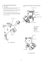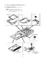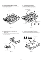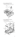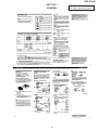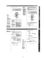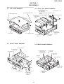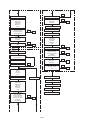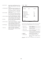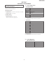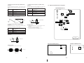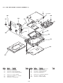
1
DVP-S3000 RMT-D100E/D100U SERVICE MANUAL US Model Canadian Model Chinese Model Hong Kong Model Singapore Model SPECIFICATIONS • Audio/video/S-link connecting cord (1) (US, Canadian) • Audio/Video connecting cord (1) (Chinese, Hong Kong, Singapore) • S video cable (1) • Remote commander (remote) RMT-D100U (1) (US, Canadian) • Remote commander (remote) RMT-D100E (Chinese, Hong Kong, Singapore) • sony R6 (size AA) batteries (2) Design and specifications are subject to change without notice. CD/DVD PLAYER MICROFILM SAFETY CHECK-OUT After correcting the original service problem, perform the following safety checks before releasing the set to the customer: 1. LEAKAGE TEST Check the area of your repair for unsoldered or poorly-soldered connections. Check the entire board surface for solder splashes and bridges. The AC leakage from any exposed metal part to earth ground and from all exposed metal parts to any exposed metal part having a return to chassis, must not exceed 0.5 mA (500 microamperes). Leakage current can be measured by any one of three methods. 2. Check the interboard wiring to ensure that no wires are “pinched” or contact high-wattage resistors. 3. Look for unauthorized replacement parts, particularly transistors, that were installed during a previous repair. Point them out to the customer and recommend their replacement. 1. A commercial leakage tester, such as the Simpson 229 or RCA WT-540A. Follow the manufacturers' instructions to use these instruments. 4. Look for parts which, though functioning, show obvious signs of deterioration. Point them out to the customer and recommend their replacement. 2. A battery-operated AC milliammeter. The Data Precision 245 digital multimeter is suitable for this job. 3. Measuring the voltage drop across a resistor by means of a VOM or battery-operated AC voltmeter. The “limit” indication is 0.75V, so analog meters must have an accurate lowvoltage scale. The Simpson 250 and Sanwa SH-63Trd are examples of a passive VOM that is suitable. Nearly all battery operated digital multimeters that have a 2V AC range are suitable. (See Fig. A) 5. Check the line cord for cracks and abrasion. Recommend the replacement of any such line cord to the customer. 6. Check the B+ voltage to see it is at the values specified. 7. Check the antenna terminals, metal trim, “metallized” knobs, screws, and all other exposed metal parts for AC leakage. Check leakage as described below. To Exposed Metal Parts on Set WARNING!! 0.15 µF 1.5 k Ω WHEN SERVICING, DO NOT APPROACH THE LASER EXIT WITH THE EYE TOO CLOSELY. IN CASE IT IS NECESSARY TO CONFIRM LASER BEAM EMISSION, BE SURE TO OBSERVE FROM A DISTANCE OF MORE THAN 25 cm FROM THE SURFACE OF THE OBJECTIVE LENS ON THE OPTICAL PICK-UP BLOCK. AC Voltmeter (0.75 V) Earth Ground CAUTION: Fig. A Using AC voltmeter to check AC leakage The use of optical instrument with this product will increase eye hazard. CAUTION Use of controls or adjustments or performance procedures other than those specified herein may result in hazardous radiation exposure. SAFETY-RELATED COMPONENT WARNING!! ATTENTION AU COMPOSANT AYANT RAPPORT À LA SÉCURITÉ! COMPONENTS IDENTIFIED BY MARK ! OR DOTTED LINE WITH MARK ! ON THE SCHEMATIC DIAGRAMS AND IN THE PARTS LIST ARE CRITICAL TO SAFE OPERATION. REPLACE THESE COMPONENTS WITH SONY PARTS WHOSE PART NUMBERS APPEAR AS SHOWN IN THIS MANUAL OR IN SUPPLEMENTS PUBLISHED BY SONY. LES COMPOSANTS IDENTIFIÉS PAR UNE MARQUE ! SUR LES DIAGRAMMES SCHÉMATIQUES ET LA LISTE DES PIÈCES SONT CRITIQUES POUR LA SÉCURITÉ DE FONCTIONNEMENT. NE REMPLACER CES COM- POSANTS QUE PAR DES PIÈCES SONY DONT LES NUMÉROS SONT DONNÉS DANS CE MANUEL OU DANS LES SUPPLÉMENTS PUBLIÉS PAR SONY. –2– TABLE OF CONTENTS Section Title Page Section Title Page Service Note ............................................................................. 4 5. IC PIN FUNCTION DESCRIPTION 1. 5-1. 5-2. 5-3. 5-4. 5-5. 5-6. 5-7 5-8 Interface Control Pin Function (MB-75 Board IC021) ..... 5-1 Drive Control Pin Function (MB-75 Board IC136) ........... 5-2 Extended Output Port 0 (MB-75 Board IC147) ............... 5-3 Extended Output Port 1 (MB-75 Board IC148) ............... 5-3 Extended Output Port 2 (MB-75 Board IC149) ............... 5-3 Extended Output Port 3 (MB-75 Board IC150) ............... 5-3 D/A Converter (MB-75 Board IC722) .............................. 5-3 System Control Pin Function (MB-75 Board IC090) ....... 5-4 GENERAL This Player Can Play the Following Discs ....................... 1-1 Getting Started ............................................................... 1-1 Basic Operations ............................................................ 1-2 Playing Discs in Various Modes ...................................... 1-8 Setting and Adjustments ................................................. 1-10 Additional Information ..................................................... 1-12 2. DISASSEMBLY 2-1. 2-2. 2-3. 2-4. 2-5. 2-6. 2-7. 2-8. 2-9. 2-10. Top Case Removal .......................................................... 2-1 Front Panel Removal ...................................................... 2-1 AU-201, 203 Board Removal .......................................... 2-1 MB-80 Board Removal .................................................... 2-1 MD Block Ass’y Removal ................................................ 2-2 Try Removal .................................................................... 2-2 Optical Pick-up Removal ................................................. 2-2 TT-40 Board Removal ..................................................... 2-2 Internal Views ................................................................. 2-3 Circuit Boards ................................................................. 2-4 3. BLOCK DIAGRAMS 3-1. 3-2. 3-3. 3-4. 3-5. 3-6. 3-7. 3-8. 3-9. Overall Block Diagram 1 (RF, Servo, Audio Power) ........ 3-1 Overall Block Diagram 2 (Signal Process) ...................... 3-6 RF/Servo Block Diagram ................................................ 3-11 Data Process Block Diagram .......................................... 3-14 Video Block Diagram ...................................................... 3-16 System Control Block Diagram ....................................... 3-21 Audio Block Diagram ...................................................... 3-24 Mode Control Block Diagram .......................................... 3-27 Power Supply Block Diagram .......................................... 3-30 4. PRINTED WIRING BOARDS AND SCHEMATIC DIAGRAMS 4-1. 4-2. Frame Schematic Diagram ............................................. 4-1 Printed Wiring Boards and Schematic Diagrams ............ 4-5 TT-40, LM-56 Printed Wiring Boards ............................... 4-5 TT-40, LM-56 Schematic Diagram .................................. 4-7 MB-80 Printed Wiring Board ........................................... 4-12 MB-80 (Interface) Schematic Diagram ............................ 4-17 MB-80 (CPU) Schematic Diagram .................................. 4-21 MB-80 (Drive Control) Schematic Diagram ..................... 4-25 MB-80 (DVD Data Process) Schematic Diagram ............ 4-28 MB-80 (CD ROM Decode) Schematic Diagram .............. 4-31 MB-80 (MPEG Video Decode) Schematic Diagram ........ 4-35 MB-80 (Video EQ, Letter Box, Sub Picture) Schematic Diagram ........................................................ 4-39 MB-80 (Audio Decode) Schematic Diagram ................... 4-42 MB-80 (Video) Schematic Diagram ................................ 4-45 MB-80 (Digital Servo) Schematic Diagram ..................... 4-51 MB-80 (RF Block) Schematic Diagram ........................... 4-55 MB-80 (Drive) Schematic Diagram ................................. 4-59 FP-611/619, PW-116/117 Printed Wiring Boards ............ 4-63 FP-611/619, PW-116/117 Schematic Diagram ................ 4-65 AU-201/203, PS-408/413 Schematic Diagram ............... 4-67 AU-201/203, PS-408/413 Printed Wiring Boards ............ 4-71 SR-740, SUB Printed Wiring Boards and Schematic Diagram ......................................................... 4-74 SR-745, SUB Printed Wiring Boards and Schematic Diagram ......................................................... 4-77 6. TEST MODE 6-1. Starting up Test Mode ..................................................... 6-1 6-2. Syscon Diagnosis ........................................................... 6-1 6-3. Drive Auto Adjustment .................................................... 6-10 6-4. Drive Manual Operation .................................................. 6-13 6-4-1. Drive Manual Operation wnu creen ........................... 6-13 6-4-2. Disc Type ................................................................... 6-13 6-4-3. Manual Control 1 ....................................................... 6-13 6-4-4. Manual Control 2 ....................................................... 6-14 6-4-5. Manual Control 3 ....................................................... 6-14 6-4-6. Manual Adjust 1 ......................................................... 6-15 6-4-7. Manual Adjust 2 ......................................................... 6-15 6-4-8. Auto Adjust ................................................................ 6-15 6-4-9. Check ......................................................................... 6-16 6-5. Emergency History ......................................................... 6-18 6-6. Other Checks .................................................................. 6-18 7. ELECTRICAL ADJUSTMENT 7-1. 1. 2. 7-2. 7-3. 1. 2. 3. 4. 5. 6. 7. 8. 7-4. 1. 2. 3. 4. 5. 6. 7. 7-5. Power Supply Check ....................................................... 7-1 PS-408/413 Board .......................................................... 7-1 MB-80 Board ................................................................... 7-1 +5.2 V Adjustment ........................................................... 7-1 Adjustment of System Control ........................................ 7-2 27 MHz Free Run ............................................................ 7-2 22 MHz Adjustment ........................................................ 7-2 33 MHz Check ................................................................ 7-2 33 MHz Lock Check ........................................................ 7-2 24 MHz Adjustment ........................................................ 7-3 36 MHz Check ................................................................ 7-3 36 MHz Lock Check ........................................................ 7-3 16 MHz Check ................................................................ 7-3 Adjustment of Video System Video Level Adjustment .................................................. 7-4 S-Terminal Output Check ................................................ 7-4 Checking Composite Video Output B-Y .......................... 7-4 Checking Composite Video Output R-Y .......................... 7-5 Checking Composite Video Output Y .............................. 7-5 Checking S Video Output S-C ........................................ 7-5 Checking S Video Output DC Level ................................ 7-5 Adjustment Related Parts Arrangement ......................... 7-6 8. REPAIR PARTS LIST 8-1. Exploded Views .............................................................. 8-1 8-1-1. Case Assembly .......................................................... 8-1 8-1-2. Front Panel Assembly ................................................ 8-2 8-1-3. Chassis Assembly ..................................................... 8-3 8-1-4. DVD Mechanism Chassis Assembly (1) .................... 8-4 8-1-5. DVD Mechanism Chassis Assembly (2) .................... 8-5 8-2. Electrical Parts List ......................................................... 8-6 –3– SERVICE NOTE 1. DISK REMOVAL PROCEDURE (at POWER OFF) 1) 2) 3. HOW TO SERVICE THE MD BLOCK ASS’Y 1) 2) Insert a cross-tip screwdriver into a hole at the bottom, and rotate the cam gear 1 in direction A. (See Fig. 1) Note: To prevent a damege of cam gear, rotate it in direction A by 1/4 turn. Draw out the tray 2 in direction B by hand, and remove a disk. (See Fig. 1) 3) 4) Remove the top case from the main unit. (Refer to 2-1) Remove the front panel. (Refer to 2-2) Note: Do not disconnect wiring. Remove the MD block ass’y. (Refer to 2-5) Remove the MD upper cover, and mount as shown in Fig. 3. Claws MD upper cover 1 Cam gear B 2 Tray Hole A Fig. 1 2. HOW TO SERVICE AU-201, 203 AND MB80 BOARDS 1) 2) Remove the top case from the set. (Refer to 2-1) Remove the AU-201, 203 board. (Refer to 2-3) Note: Do not disconnect wiring. Remove the MB-80 board. (Refer to 2-4) Note: Do not disconnect wiring. Erect MB-80 board on three circuit board holders. (See. Fig. 2) Erect AU-201, 203 board on two claws. (See Fig. 2) 3) 4) 5) MB-80 board Front panel Fig. 3 5) 6) Install the MD block ass’y as shown in Fig. 4. Note: Place a cushion at the position A. Connect three flexible flat cables. MD block ass’y MD upper cover AU-201 board (US, Canadian model) AU-203 board (Chinese, Hong Kong, Singapore model) MD block ass’y Three flexible flat cable Two claws Three circuit board holders A Fig. 2 Fig. 4 –4– 4. NOTE ON MOUNTEING SLED MOTOR 1) 2) Push the sled motor assy 1 toward direction A. (See Fig.5) Tighten two screws 2 (M1.7 × 2.5). 1 Sled motor ass’y A 2 Two screws (M1.7 × 2.5) Fig. 5 3) 4) Raising the MD block assy 3 90 º with the side down. confirm that the optical pick-up 4 falls by self weight. (See Fig. 6) Further, with the front side of MD block assy 3 up, confirm that the optical pick-up falls by self weight. 3 MD block ass’y Upper Upper Lower Front side Lower 4 Optical pick-up Fig. 6 –5– Front side 5. REPLACING OPTICAL PICK-UP 5-1. 3) Handling 1) A red laser diode for DVD requires more attention to static electricity than general infrared laser diodes for CD. Because its durability to static electricity is far weaker than that of infrared laser diodes, always use an earth band when handling the optical pick-up block as service parts. 2) As for the flexible board KHS-180A (RP) packed as service parts, the short lands have been soldered to protect from static electricity. Accordingly, remove solders when replacing optical pick-up. (See Fig. 7) In handling the KHS-180A (RP), do not touch inhibited parts shown in Fig. 8, but grip the slide base bearing and U-shaped guide. Slide base bearing Skew sensor Lens actuator covers Objective lenses DVD short land Laser holder U-shaped guide OEIC Touch inhibited parts • Objective lens • Skew sensor • Laser holder • Laser coupler • Flexible board • OEIC • Lens actuator covers CD short land Flexible board Connector Fig. 7 Flexible board Laser coupler Fig. 8 KHS-180A (RP) –6– 6. NOTE ON ASSEMBLING MECHANICAL DECK 6-1. 1) Application of Grease Grease must be applied if the following parts were replaced. (See Fig. 9) NOTE 1: Recommended grease is Foil KG-70MP. NOTE 2: In applying grease, take care not to allow grease to stick to other parts (particularly, rubber belt, spindle motor, and optical pick-up) Base unit holder 2 bosses Slide base Skew cam Cam gear Tray 3 grooves NOTE: Add grease if tray moves slowly. Loading pulley shaft NOTE: Add grease if tray generates noise periodically. Fig. 9 –7– 6-2. Cleaning Spindle Motor Turntable 6-4. Deformation of Insulator 1) 2) 1) 2) 3) Remove the tray. (Refer to 2-6) Clean the spindle motor turntable if disc antiskid rubber (black) is dirty. (See Fig.10) Assemble the spindle base into the base unit. Lock with 4 shoulder screws. (See Fig.12) Check if 4 insulators deformed. (See Fig.12) Four step screws Spindle motor Turntable Two insulators Insulator Two insulators Good Fig. 12 Fig. 10 6-5. Note on connecting OPT Harness 6-3. Aligning Phase of Cam Gear and Drive Gear 1) 1) Align triangle marks when assembling the cam gear and drive gear. (See Fig.11) The optical pick-up could be destroyed unless the OPT harness is connected normally to the connector. (See Fig.13) OPT harness Good NG Connector Drive gear NG Cam gear Align triangle marks. Fig. 11 Fig. 13 –8– 6-6. Note on Mounting LM-51 Board 1) 2) Align two bosses. (See Fig.14) Fix the board securely with screws (PTPWH 2 × 5). (The sensor will not function normally if the board floats up.) Screw (PTPWH2 × 5) LM-56 board Two bosses Fig.14 6-7. Note on Mounting TT-701 Board 1) 2) 3) Align two bosses. (See Fig.15) Align four tabs. (See Fig.15) Fix the board securely with 3 screws (BV 3 × 10). (The sensor will not function normally if the board floats up.) Three screws (BV3 × 10) TT-40 board Boss Two claws Two claws Boss Fig.15 –9– DVP-S3000 SECTION 1 GENERAL 1-1 This section is extracted from US model instruction manual. 1-2 1-3 1-4 1-5 1-6 1-7 1-8 1-9 1-10 1-11 1-12E 1-12 DVP-S3000 SECTION 2 DISASSEMBLY Note: Follow the disassembly procedure in the numerical order given. 2-1. TOP CASE REMOVAL 2-3. AU-201, 203 BOARD REMOVAL 8 AU-201 board (US, Canadian model) AU-203 board (Chinese, Hong Kong, Singapore model) 2 Three tapping screws 1 Two tapping screws 2 Connector (CN954) 1 Flexible flat cable (FAM-5) (CN381) 4 Top case 6 Two tapping screws 3 Two tapping screws 3 Connector (CN011) 2-2. FRONT PANEL REMOVAL 7 Screw (BV3 × 10) 5 Connector (CN382) 4 Flexible flat cable (FAM-6) (CN005) 2-4. MB-80 BOARD REMOVAL 2 Three bosses 1 Two screws (BV3 × 10) 3 Two claws 1 Three flexible flat cables (FTM-3) (CN885/886/980) 4 Screw (BV3 × 10) 2 Connector (CN001) 5 Two screws (BV3 × 10) 7 MB-80 board 6 Three screws (BV3 × 10) 5 claw 6 Front panel 3 Flexible flat cable (FTT-4) (CN009) 4 Two claws 7 Flexible flat cable (FTT-4) (CN101) 2-1 2-5. MD BLOCK ASS’Y REMOVAL 2 Three screws (BV3 × 10) 2-7. OPTICAL PICK-UP REMOVAL 3 MD block ass’y 4 Optical pick-up 3 Main shaft 1 Three flexible flat cables (FTM-3) (CN005/006/007) 2 screw (PTTWH2 × 5) 1 OP-15 flexible board (CN001) 2-8. TT-40 BOARD REMOVAL 2-6. TRAY REMOVAL 5 Four screws (BV3 × 10) 1 Two screws (BV3 × 10) 7 TT-40 board 3 MD upper cover 4 Two screws (BV3 × 10) 2 Flat cable (spindle motor) (CN002) 5 Press pully bracket 1 Connector (CN004) 7 Pull the tray to direction of the arrow B. 9 Remove the tray 3 LT-31 flexible board (CN003) 4 OP-15 flexible board (CN001) 2 claw A B 8 claw 6 Two claws 6 Rotate the cam gear to direction of the arrow A . 2-2 2-9. INTERNAL VIEWS Skew motor ass’y X-3947-138-1 Optical pick-up (KHS-180A/J1N) 8-820-005-02 Sled motor ass’y X-3947-137-1 Sled motor ass’y X-3947-137-1 Optical pick-up (KHS-180A/J1N) 8-820-005-02 DC motor (spindle) 1-698-944-11 KU160 (CD sensor) 8-749-013-33 DC motor (spindle) 1-698-944-11 Motor (loading) 1-698-942-21 2-3 2-10. CIRCUIT BOARD LOCATION SR-740 (US, Canadian model) SR-745 (Chinese, Hong Kong, Singapore model) SWITCHING REGULATOR LM-56 (SLED) PS-408 (US, Canadian model) PS-413 (Chinese, Hong Kong, Singapore model) (POWER) AU-201 (US, Canadian model) AU-203 (Chinese, Hong Kong, Singapore model) (AUDIO) TT-40 (RF/SERVO) PW-116 (US, Canadian model) PW-117 (Chinese, Hong Kong, Singapore model) (IR/POWER SWITCH) DC MOTOR (SPINDLE) FP-611 (US, Canadian model) FP-619 (Chinese, Hong Kong, Singapore model) (FL DRIVER/FUNCTION SWITCH) 2-4E 2-4 MB-80 (SIGNAL PROCESS/SERVO) 5-1. INTERFACE CONTROL PIN FUNCTION (IC021 on MB-80 Board (1/12)) Pin No. Pin Name I/O 1,2 CL1, 0 I Input of sub clock (32kHz) Function 3,4 GND – Ground 5,6 X0–1 I Input of main clock (8MHz) 7 GND – 8 RST I Pin No. Pin Name I/O 59-66 N.C. – Function Not used 67 VCC – Power supply 68-75 N.C. – Not used Ground 76 CS I CS (SYSCON) Input of RESET signal 77 SI I SI (SYSCON) RESET O SRESET (SYSCON) 78 SO O SO (SYSCON) INTMS O XINTM S (SYSCON) 79 CLK I CLK (SYSCON) 80-82 N.C. – Not used 83 GND – Ground 84-87 AD0–3 I Analog input 11 AUDIO MUTE O SAUDIO MUTE (L) 12 IFDIAG I DIAG (H) 13 NITSC O NTSC (H) /PAL (L) 14,15 N.C. – Not used 88 TEST 1 I Input of TEST 1 signal 16 FLCS O XFLCS (FL) 89 TEST 2 I Input of TEST 2 signal 17 REF V I XREF-V (VSYNC) 90 N.C. – Not used 18 INTSM I XINTSM (SYSCON) 91 N.C. – Not used 5-1 N.C. – Not used 92 VCC – Power supply 25 POWER CONT O POWER-CONT (H) 93 POWER-FAIL I Input of POWER-FAIL (AD INPUT) 26 DATA BOUND O DATA-BOUND 94 N.C. – Not used 27 N.C. – Not used 95 CGRA 16 I CGRA16 Character generator font ROM address 16 28 CMOD I CMOD 96 CGRA 17 I CGRA17 Character generator font ROM address 17 29 P.FAIL O Power fail 97 CGRA 18 I CGRA18 Character generator font ROM address 18 30 CGSO O CGSO (FL & OSDC) 98 N.C. – Not used 31 CGCLK O CGCLK (FL & OSDC) 99 N.C. – Not used 32 WSIRCS I WSIRCS 100 VCC – Power supply 33 CGCS O CGCS (OSDC) 34 V MUTE O Video mute 35 STATUS O STATUS (H) 36 N.C. – TSEL (OSDC) Not used 37 STATUS O FSEL (OSDC) 38 N.C. – TRE (OSDC) Not used 39-48 N.C. – Not used 49 VCC – Power supply 50-57 N.C. – Not used 58 GND – Ground DVP-S3000 19-24 5. IC PIN FUNCTION DESCRIPTION 9 10 5-2. DRIVE CONTROL PIN FUNCTION (IC136 on MB-80 Board (3/12)) Pin No. 1 Pin Name VCC I/O – 2 MRST O 3 12 RST 4 CD DET 5 TRAY OUT 6 CHUCK Function Pin No. 65 Pin Name VSS I/O – Peripheral circuits reset signal (L: Reset) 66 EXTAL I Input of 16.9MHz O 12V system power control signal 67 XTAL I Input of 16.9MHz I Input of DVD/CD discriminate sensor 68 VCC – Power supply I Tray out end (H: End) 69 AS O Address strobe I Chucking down end (H: End) 70 RD O Read 71 HWR O H_Write Power supply 7 LOCK I Good Frame Sync dat (H: OK, L: NG) 8 XPNM I RF Pro PLL Mode (L: Normal) 9 FOK I Focus OK (H: OK, L: NG) 10 N.C. – 11 VSS – Function Ground 72 LWR O L_Write 73–75 MD0–2 I Operation mode setting (Mode 2) Not used 76 A VCC – Power supply Ground 77 VREF – Reference voltage 12 CPDTO O Serial data output to each IC 78 N.C. – Not used 13 SDCS (SO) O Serial data output to jig 79 HYDET1 I Input of sled FG2 5-2 14 CPDTI I Serial data input from each IC 80 P FAIL I Power down pre signal 15 SDSC (SI) I Serial data input from jig 81 PI I Input of pull–in signal 16 CPCK O Serial clock to each IC 82 SLD2– I Input of sled offset 17 SCKCS O Serial clock to jig 83 SLD2+ I Input of sled offset 18–21 D0–3 I/O Data bus 0–3 84 VCOM I Input of VCO adjustment 22 VSS – Ground 85 JIG BUSY I Serial busy signal from Jig 23–25 D4–6 I/O Data bus 4–6 86 A VSS – Ground 26–34 D7–15 I/O Data bus 7–15 87 SCOR I CXD2545 address storing request signal 35 VCC – Power supply 88 INT-SC I Serial data 36–43 A0–7 O Address bus 0–7 89 SOINT I Jitter storing request signal 44 VSS – Ground 90 SYS_INT I Interrupt request signal from Syscon 45–50 A8–13 O Address bus 8–13 91 ROM BUSY I EEPROM Ready/Busy signal 51–56 A14–19 O Address bus 14–19 92 VSS I Ground 57 VSS – Ground 93 TKC I Input of sled FG count 58 WAIT I WAIT signal (fixed to “H”) 94 FCMPL I FEZC Low det 59 BREQ I Input of bus request 95 FCMPH O FEZC High det 60 BACK O Output of bus ACK 96 SENS I Input of SENS signal 61 SYS CLK O Output of system clock (for check) 97 HFG I Input of spindle FG 62 STBY I Fixed to “H” 98 DVDLDON O LD ON/OFF control for DVD 63 RES I Input of Reset by SH (L: Reset) 99 CDLCON O LD ON/OFF control for CD 64 NMI I Fixed to “L” 100 LT MUTE O 5-3. EXTENDED OUTPUT PORT0 (IC147 on MB-80 Board (3/12)) Pin No. Pin Name 2 SQCK MSK I/O O Function SubQ Read Clock Mask 5-6. EXTENDED OUTPUT PORT3 (IC150 on MB-80 Board (3/12)) Pin No. 2 Pin Name TILT/H I/O O Function Tilt Filter change 5 ROM CS O Chip Select for EEPROM 5 SPGC1 O Selection of low band boost (H: 12 cm, L: 8 cm) 6 DA XLD O Load Signal for D/A 6 CD/DVD O DVD/CD (H: DVD, L: CD) 9 SUBQ XOE O SubQ Output Enable 9 Q4 – Not used 12 XLAT O Latch Signal for CXD2545 12 SPCTL0 O Spindle Control [SPCTL0: SPCTL1] 15 SPCTL1 O 15 SDEN O Serial Output Enable For SSI3720 16 SLD MODE O Sled Control change 19 INT CS O Serial data forward request 5-4. [0: 0] = control, [0: 1] = not control, [1: 0] = acceleration, [1: 1] = deceleration 16 CLVH O Spindle CLVH Control 19 Q8 – Not used EXTENDED OUTPUT PORT1 (IC148 on MB-80 Board (3/12)) 5-3 Pin No. 2 Pin Name XLT I/O O Function Latch Signal for RF Pro 5 SOEN O Serial Output Enable for RF Pro 6 SCK MSK O 9 SCLK 12 5-7. D/A CONVERTER (IC722 on MB-75 Board (10/12)) Pin No. 1 Pin Name VSS I/O – Serial command transfer clock master 2 HYCNTR O Adjustment of hall element output O SENS reading clock 3 SDCNTR O Target sled speed FJUMP- O Focus Jump Pulse 4 TI OFFSET O Tilt sensor offset output 15 FJUMP+ O Focus Jump Pulse 5 LOAD/UNLOAD O Loading/Unloading Control 16 DRV BUSY O Communication inhibit request from system controller 6 TI DRIVE O For tilt forced movement 19 LOCK MON O Spindle LOCK Monitor Out 7 SDINIT O Offset adjusting signal of sled motor drive 8 VDD – Power supply 5-5. EXTENDED OUTPUT PORT2 (IC149 on MB-80 Board (3/12)) Function Ground 9 VCC – Power supply 10 A08 – Not used Function Interrupt request to system controller 11 DO O Serial Data Output 12 LD I Serial Data Load O Spindle forced stop (L: Stop) Active only at out of control 13 CLK I Serial Clock Input O Focus Hold 14 DI I Serial Data Input AVCO O For VCO adjustment GND – Ground Pin No. 2 Pin Name DRV INT I/O O 5 NST 6 FHOLD 9 FDWN O Focus Gain Down (L: Normal) 15 12 LOAD ON O Loading/Unloading Moter ON/OFF 16 15 DET ON O CD Det Sensor LED ON/OFF 16 LP ON O VCO Control 19 MUTE O Date output (CXD2545) control 5-8. SYSTEM CONTROL PIN FUNCTION (IC090 on MB-80 Board (2/12)) Pin No. Pin Name I/O Function Pin No. 66 Pin Name IRQ0 I/O I 1 IRQ6 I Input of interrupt from CXD1186, CXD8663Q, CXD8669Q 2 IRQ7 I 3 VSS – Function Input of interrupt signal from SP, BFD, drive controller Input of interrupt from CXD1900 67 DREQ0 I Input of DMA request from CK Digital ground 68 IRQ2 I Input of VSYNC (FID) interrupt signal Data bus AD0-AD7 69 IRQ3 I Input of interrupt signal from CK, DSP5600 Digital ground 70 VCC – Digital power supply 4–11 AD0–7 I/O 12 VSS – 13,14 AD8–9 I/O Data bus AD8, AD9 71 CK O Output of internal clock 15 VCC – Digital power supply 72 VSS – Digital ground 16–21 AD10–15 I/O Data bus AD10-AD15 73 EXTAL – 20MHz crystal connection pin 22 VSS – Digital ground 74 XTAL – 20MHz crystal connection pin 23–30 A0–7 O Address bus A0-A7 75 VCC – Digital power supply 31 VSS – Digital ground 76 NMI – Not used 32–39 A8–15 O Address bus A8-A15 77 VCC – Digital power supply WDTOVF – Not used 40 VSS – Digital ground 78 41,42 A16–17 O Address bus A16, A17 79 RES I Input of reset signal 5-4 43 VCC – Digital power supply 80 MD0 I Input of mode select 0 (fixed to “1”) 44–47 A18–21 O Address bus A18-A21 81 MD1 I Input of mode select 1 (fixed to “0”) 48 CS0 O Chip select signal for external ROM 82 MD2 I Input of mode select 2 (fixed to “0”) 49 CS1 O Chip select signal for external RAM 83,84 VCC – Digital power supply 50 CS2 – Not used 85 AVCC – Analog power supply 51 CS3 O Chip select signal for RAM common to drive controller 86 AVREF – Reference power supply 52 VSS – Digital ground 87 PC0 I Input of DIAG mode select signal 53 PA0 O Not used 88 PC1 I Input of EMPH signal from CXD2545 54 PA1 O Output of squeeze mode 89 PC2 I Input of request from drive controller PC3 I Input of request from DSP56000 55 CS6 O Output of chip select signal to external device 90 56 WAIT I Input of wait signal 91 AVSS – Analog ground 57 WR O Output of write signal 92 PC4 I Input of FID signal from CXD1914 58 PA5 O Output of IF controller serial data control 93 PC5 I Input of request from I/F controller 59 RD O Output of read signal 94 PC6 I Input of control 1 60 PA7 O Not used 95 PC7 I Input of control 2 61 VSS – Digital ground 96 VSS – Digital ground 62 PA8 O Output of serial select signal to L chip 97 PB0 O Output of request to I/F controller 63 PA9 O Output of serial select signal to CXD1914 98 PB1 O Output of request to drive controller 64 PA10 O Output of serial select signal to audio DAC 99 VCC – Digital power supply 65 PA11 O Output of error free signal 100 PB2 O Output of clock system switching (DVD/CD) Pin No. Pin Name I/O Function 101 PB3 O Output of reset signal to audio DAC 102 PB4 O Output of reset signal to peripheral device 103 PB5 O Output of serial select signal to DSP56000 104 PB6 O Output of HREQ signal latch reset to DSP56000 105 PB7 O Output of serial select signal to video equalizer 106 VSS – Digital ground 107 RxD0 I Input of serial data from other than CXD1914 108 TxDO1 O Output of serial data to other than CXD1914 109 RxD1 I Input of serial data from CXD1914 110 TxD1 O Output of serial data to CXD1914 111 SCK0 O Output of serial clock to other than CXD1914 112 SCK1 O Output of serial clock to CXD1914 5-5 E 5-5 DVP-S3000 SECTION 6 TEST MODE 6-1. Starting up Test Mode If [0] key on standard commander is pressed during initial menu display, the Diagnosis screen as shown in Figure 2 is displayed, and a checking starts from the top of diagnosis check items list sequentially. After a checking started, standard commander keys are accepted while a message or title is blinking, so that you can go to the next job. With the DVP-S3000 in standby status, press [TIME], [CLEAR], and [POWER] keys on the standard commander in this order. And, the Test mode starts up and the initial menu shown in Figure 1 appears on the video display. Test Mode Menu Syscon Diagnosis 0. Syscon Diagnosis 1. Drive Auto Adjustment IF con SYScon Ver.x.xx (xxxx) Ver.x.xx (0000) DRVcon Ver.0.00 (0000) 2. Drive Manual Operation 3. Emergency History ROM Check 4.OtherChecks SIRCS:ff KEY:ff RATE: 29 Exit: POWER Key Figure 2 Figure 1 Initial menu In this mode, ROM revision number (Ver. No.) of each control IC (MPU) and its checksum are displayed. However, Syscon checksum and Drvcon value are obtained in the process of diagnosis check, and therefore they are initially 0. On the fifth line, an item is displayed, and IF control information is displayed at the bottom though it is not related to a checking of each item. If Syscon Diagnosis is selected, a checking starts immediately, and the result of initial ROM check and Syscon ROM checksum are displayed as shown in Figure 3. In the Test mode, necessary operations are all done with the keys on standard commander or operation panel. The test mode can be finished and the set returns to the power off status when the [POWER] key is pressed whichever mode, except during checking of Syscon Diagnosis, you are working in now. 6-2. Syscon Diagnosis In the Syscon Diagnosis, intermittent blocks such as 0-ff, 500-5ff, a00-aff, f00-fff, 1400-14ff, etc. (address) are checked. All of the operation are done with standard commander keys, and a menu cannot be selected but all items are checked. After result display, you can only select either “continue to next item” or “cancel”, and continue and retry in case of written data error are not available. Syscon Diagnosis IF con SYScon Ver.x.xx (xxxx) Ver.x.xx (xxxx) DRVcon Ver.0.00 (0000) ROM Check ★★ Press Remocon Key★★ SIRCS:ff KEY:ff RATE: 29 Figure 3 6-1 N Data in ( ) indicates Syscon checksum (2-3) Syscon RAM (IC094) check Confirm the result, and to cancel checking, press [RETURN], [MENU], or [POWER]. Or, to continue next checking, press other than these keys. The ROM revision and checksum of Drvcon are displayed when executing “DrvCon Data Exchange” and “DrvCon EPROM” respectively. Also, in case of an error, the error code and information are displayed as shown in Figure 4. IC093 (Syscon ROM) n IC094 (Syscon RAM) collating check Checking range: 0x01000000 - 0x0101ffff IC093 (Syscon ROM) data (program codes) are transferred in DMA mode in the unit of 64 bytes to the IC094 (Syscon RAM), then they are read every 1 byte and compared with data in IC093. As the Syscon RAM check is made by saving the data into internal RAM (DMA transfer), the data are written and read every 64 bytes, and interruption during that time is completely masked. If compared data are not same, a checking is suspended, and error code 05, its address, written data, and read data are displayed. Select the subsequent processing by pressing a key. As this check is made through DMA transfer, if Repeat is selected, the data are transferred in DMA mode again to the block where this error occurred and a checking is continued from the error address. Syscon Diagnosis IF con Ver.x.xx (xxxx) SYScon DRVcon Ver.x.xx (xxxx) Ver.x.xx (xxxx) CXD 1900BQ DRAM Error Code: 05 Address: 000abcde Write Data: fb Read Data: ff N Name of item checked N Error code N Error address (3) Clock N Written data (2/4 digits) N Read data (2/4 digits) (3-2) Audio clock system output switching (CD side) I/O output The audio clock system is switched to the CD side. In this check, the Syscon itself does not detect an error. Observe output signals with an instrument. SIRCS:ff KEY:ff RATE: 29 Figure 4 (3-3) Audio clock system output switching (DVD side) Except error code “05” (write/read data mismatch error), the address and data fields show “0”. When a checking is over or cancelled, “Diag OK” or “Diag Error End” message blinks. If a key is pressed here, the test mode initial menu is resumed. The “Diag Error End” is displayed only when the Syscon detects an error, and visual inspection result is out of the display. I/O output The audio clock system is switched to the DVD side. In this check, the Syscon itself does not detect an error. Observe output signals with an instrument. (4) Drvcon 6-2-1. General description of checking method (4-2) Drvcon (IC136) reset check This section describes briefly a checking method for each item in the order of menus. Numbers in ( ) for respective items are diagnosis item numbers. Hard Reset n DRV BUSY response input The Hard Reset signal is output, and after cancelling the reset, whether DRV BUSY signal changes from “low” to “high” is checked. The detection timing of DRV BUSY “low” is about 250 msec after the reset is cancelled. Also, whether the signal becomes “high” later is checked. (2) Memory (2-2) Syscon ROM (IC093) check Calculation of checksum After confirming “high” or “low” of DRV BUSY signal 250 msec after reset was cancelled, if the signal does not go “high” though about 300 msec elapsed, the reset error 02 is output. Calculation range: 0x00000000 - 0x000fffff (at commercial products, 8Mbit ROM) All 8bit data from address 0 to ROM size are added (checksum), and output as 4-digit hexadecimal number. In this check, the IC090 (Syscon) itself does not detect an error. The result is displayed on the screen. Compare it with original ROM checksum. 6-2 (4-3) Drvcon common RAM (IC138) check (4-6) Drvcon SRAM check IC093 (Syscon ROM) n IC138 (common RAM) collating check IC090 (Syscon) n IC136 (Drvcon) check request command Checking range: 0x03000001 - 0x03000fff The SRAM check command is sent from IC090 to IC136, and its response result is displayed. In case of an error, the error information of Drvcon is read, then the error code 05, error address, written data, and read data are displayed. After confirming that the RAM areas common to Drvcon are not occupied by Drvcon (namely, the contents of common RAM addresses are true), the IC093 (Syscon RAM) codes are copied to the IC138 (common RAM) areas from address 1, then the data are read for checking. If all are same, the IC093 code bits are inverted and checked again. If compared data are not same, a checking is suspended, and error code 05, its address, written data, and read data are displayed. After checking, reset the Drvcon because irregular values are written to the IC138. (4-7) EEPROM check IC090 (Syscon) n IC136 (Drvcon) check request command If common RAM areas are occupied by Drvcon and they are not opened even after about 2 seconds, the write error 03 is output. The EEPROM check command is sent from IC090 to IC136, and its response result is displayed. The error code 74 when IC139 (EEPROM) write signal is not ready, or error code 05 when written data and read data are not same, error address, written data, and read data are displayed. (4-4) Drvcon data exchange check (4-8) RF Processor check IC090 (Syscon) n IC136 (Drvcon), IC136 (Drvcon) n IC090 (Syscon) command path check IC090 (Syscon) n IC136 (Drvcon) check request command The RF processor check command is sent from IC090 to IC136, and its response result is displayed. In case of an error in IC770 (RF processor), the error code 76 is output. The path check command is sent from IC090 (Syscon) to IC136 (Drvcon), and as a result, whether the data same as sent data is returned to the IC138 (common RAM) is checked. In the Syscon Diagnosis, only the ROM revision is displayed. If no response is returned from Drvcon or the data are not same, the error code 73 is output. (4-9) CXD2545 RAM check The CXD2545 check command is sent from IC090 to IC136, and its response result is displayed. In case of an error in IC717 (CXD2545), the error code 75 is output. (4-5) Drvcon interrupt line check IC136 (Drvcon) n IC090 (Syscon), IC090 (Syscon) n IC136 (Drvcon) interrupt line check (4-10) Drvcon ROM check If CXD8663Q check command is sent from IC090 to IC136, the IC136 returns IC181 (CXD8663Q) register read/write command. Receiving this command, the IC090 outputs a response signal implying that the interrupt signal was received, then the IC136 confirms this signal input and writes the Command Done to the IC138 (common RAM). When the Command Done is not returned even after 1 second, the error code 70 (DRV INT is not detected) is output if the interrupt signal has not been received, or the error code 71 (Drvcon does not recognize SYS INT) is output if the interrupt signal has been received. Also, upon detection of an error in IC181 (CXD8663Q) by this command, the error code 30 is output. IC090 n IC136 check request command The EPROM check command is sent from IC090 to IC136. The Drvcon calculates checksum of IC140 (EPROM), and returns its result and the checksum value is displayed, if there is no error. Compare the result displayed on the screen with the checksum of original EPROM. (4-11) VCO offset automatic adjustment IC090 n IC136 check request command The VCO offset automatic adjust command is sent from IC090 to IC136. If automatic adjustment failed, the error code 77 is output. If DRV INT signal is kept “low”, the Syscon repeats an interrupt processing continuously, thus making error display impossible. For this reason, only for this command, the Drvcon returns the DRV INT signal to “high” even if SYS INT is not detected. (The Syscon makes judgment whether Command Done is returned or not.) Here, if the Syscon makes no response, the DRV INT signal itself will be faulty. (5) Data supply system (5-2) IC217 (CXD8598R) reset check Write to register n Hard reset n Read from register Registers to be checked: TSC2 (0x06200011) TSC1 (0x06200012) TSC0 (0x06200013) Data other than 0 are written to readable and writable registers in IC217 (CXD8598R), and they are read after hard reset, then the error code 02 is output if they are not cleared to 0. 6-3 (5-3) IC217 (CXD8598R) register check As SERR signal from IC181 (CXD8663Q) to IC217 (CXD8598R) is not initialized, this signal line is shut off and fixed to “high” before checking. Register write n Register read collating check Registers to be checked: TSC2 (0x06200011) TSC1 (0x06200012) TSC0 (0x06200013) (5-8) IC181 (CXD8663Q) to IC217 (CXD8598R) connection check IC093 (Syscon ROM) n IC181 (CXD8663Q) n IC217 (CXD8598R) Incrementing 1 each starting from 0, data are written to readable and writable registers, then they are read for checking. Incrementing initial value by 1 each, a check is repeated 256 times. If compared data are not same, a checking is suspended, and error code 05, its address, written data, and read data are displayed. Write to register n Hard reset n Read from register DVD bit stream data stored in IC093 are transferred to the IC182 (external DRAM of IC181), and IC217 (CXD8598R) transfer end interruption is checked, which occurs by flowing data to the IC217 (CXD8598R). If the transfer end interruption is not detected, the error code 21 is output. As SERR signal from IC181 (CXD8663Q) to IC217 (CXD8598R) is not initialized, this signal line is shut off and fixed to “high” before checking. Register to be checked: INTRMASK (0x22) (5-9) IC184 (CXD8669AQ) reset check Data other than 0 are written to readable and writable register in IC181 (CXD8663Q), and they are read after hard reset, then the error code 02 is output if they are not cleared to 0. Write to register n Hard reset n Read from register (5-5) IC181 (CXD863Q) register check Data other than 0 are written to readable and writable register in IC184 (CXD8669AQ), and they are read after hard reset, then the error code 02 is output if they are not cleared to 0. (5-4) IC181 (CXD8663Q) reset check Register to be checked: SYSINI (0xe1) Register write n Register read collating check (5-10) IC184 (CXD8669AQ) register check Register mask data to be checked 0x20 0xbf 0x22 0xff 0x25 0xff 0x26 0xff 0x27 0xff Register write n Register read collating check Register mask data to be checked 0xe0 0x80 0xe1 0xff 0xe4 0xc0 0xe5 0xc0 0xe6 0xf8 Incrementing 1 each starting from 0, data are written to readable and writable registers, then they are read for checking. Incrementing initial value by 1 each, a check is repeated 256 times. However, some bits that cannot be written are masked. If compared data are not same, a checking is suspended, and error code 05, its address, written data, and read data are displayed. Incrementing 1 each starting from 0, data are written to readable and writable registers, then they are read for checking. Incrementing initial value by 1 each, a check is repeated 256 times. However, some bits that cannot be written are masked. If compared data are not same, a checking is suspended, and error code 05, its address, written data, and read data are displayed. (5-6) IC181 (CXD8663Q) DRAM check ROM n IC181 (CXD8663Q) n DRAM n IC181 (CXD8663Q) read collating check (5-11) IC216 (CXD1186) reset check Checking range: 0x00000000 - 0x0007ffff Write to register n Hard reset n Read from register ROM pattern is copied to all areas to be checked. Each time 256 bytes are copied, 255 bytes of original (ROM) address are returned. A reading check is made after data are written to all areas. If compared data are not same, a checking is suspended, and error code 05, its address, written data, and read data are displayed. Registers to be checked: DADRC_L (0x06380007) DADRC_H (0x06380008) HXFRC_L (0x06380009) HXFRC_H (0x0638000A) HADRC_L (0x0638000B) HADRC_H (0x0638000C) (5-7) IC181 (CXD8663Q) interrupt line check IC093 (Syscon ROM) n IC181 (CXD8663Q) n IC217 (CXD8598R) Data other than 0 are written to readable and writable register in IC216 (CXD1186), and they are read after hard reset, then the error code 02 is output if they are not cleared to 0. DVD bit stream data stored in IC093 are transferred to the IC182 (external DRAM of IC181), and the SD bus sector header detect interruption is checked, which occurs by flowing data to the IC217 (CXD8598R). If the header of SD bus sector in IC181 (CXD8663Q) is not detected, the error code 31 is output. 6-4 (5-12) IC216 (CXD1186) register check Incrementing 1 each starting from 0, data are written to readable and writable register, then they are read for checking. Incrementing initial value by 1 each, a check is repeated 256 times. However, some bits that cannot be written are masked. If compared data are not same, a checking is suspended, and error code 05, its address, written data, and read data are displayed. Register write n Register read collating check Registers to be checked: DADRC_L (0x06380007) DADRC_H (0x06380008) HXFRC_L (0x06380009) HXFRC_H (0x0638000A) HADRC_L (0x0638000B) HADRC_H (0x0638000C) (6-4) IC281 (CXD1900BQ) DRAM check IC093 (ROM) n IC281 n IC280, IC282 n NIC284 (DRAM) n IC281 read collating check Incrementing 1 each starting from 0, data are written to readable and writable registers, then they are read for checking. Incrementing initial value by 1 each, a check is repeated 256 times. If compared data are not same, a checking is suspended, and error code 05, its address, written data, and read data are displayed. Checking range: 0x00000000 - 0x0003ffff (data bus width = 64bits) IC093 ROM pattern is copied to all areas to be checked. Because of large DRAM capacity, each time 256 bytes are copied, 255 bytes of original (IC093) address are returned. A reading check is made after data are written to all areas. The error code 03 when writing is not ready, or error code 04 when reading is not ready is output, then a check is finished. Also, if compared data are not same, a check is suspended, and error code 05, its address, written data, and read data are displayed. However, the data are displayed every 8 bits, though the bus width of IC281 (CXD1900BQ) is 64 bits. Namely, actual address is the displayed value shifted by 3 bits to the right where lower 3 bits indicate the byte position. For example, in the case of display shown below: (5-13) IC216 (CXD1186) SRAM check IC093 (Syscon ROM) n IC216 (CXD1186) n IC215 (SRAM) n IC216 read collating check Checking range: 0x00000000 - 0x00007fff IC093 ROM pattern is copied to all areas to be checked. Each time 256 bytes are copied, 255 bytes of original (ROM) address are returned. A reading check is made after data are written to all areas. After SRAM write addresses are set, error code 03 when writing is not ready, or after read addresses are set, error code 04 when reading is not ready is output, then a check is finished. Also, if compared data are not same, a check is suspended, and error code 05, its address, written data, and read data are displayed. IC281 (CXD1900BQ) DRAM Error Code: 05 Address: 000abcde Write Data: fb Read Data: ff (5-14) IC216 (CXD1186) to IC217 (CXD8598R) connection check If displayed value 0 0 0 A B C D E is expressed with binary number, 0000 0000 0000 1010 1011 1100 1101 1110. If it is shifted by 3 bits to the right, 0000 0000 0000 0001 0101 0111 1001 1011 110. That is, assuming that the top of address 0 0 0 1 5 7 9 B in hexadecimal notation is 0th byte, the 6th byte is erroneous such as FB n FF (as for the bit position in the same manner, the 53rd bit is 0 n 1, assuming that MSB is 0th and LSB is 63rd). IC093 (ROM) n IC216 (CXD1186) n IC217 (CXD8598R) VCD bit stream data stored in IC093 are transferred to the IC215 (external SRAM of IC216), and IC217 (CXD8598R) transfer end interruption is checked, which occurs by flowing data to the IC217 (CXD8598R). If the transfer end interruption is not detected, the error code 21 is output. Further, SCR is read to check its value. If the value is not the one in sector transferred, the error code 22 is output. (6-5) CXD1914 VSync check IC475 (CXD1914Q) VSync interrupt cycle measurement (6) Video Decoder The VSync interruption is enabled for about 160msec, and the number of VSync interruption from NTSC encoder is counted. The operation is normal if the count is more than 9 times and less than 11 times. If out of this range, the error code 41 is output. The SCI1 interruption is also enabled, as the NTSC encoder processing is required due to VSync interruption. (6-2) IC281 (CXD1900BQ) reset check Write to register n Hard reset n Read from register Register to be checked: PLYMOD (0x06080002) (6-6) IC281 (CXD1900BQ) VSync interrupt line check Data other than 0 are written to readable and writable register in IC281 (CXD1900BQ), and they are read after hard reset, then the error code 02 is output if they are not cleared to 0. IC281 (CXD1900BQ) VSync interrupt detection check (6-3) IC281 (CXD1900BQ) register check The VSync interruption of IC281 (CXD1900BQ) is enabled and whether interruption is made is checked. If no interruption is made though 2 seconds elapsed, the error code 41 is output. Register write n Register read collating check (6-7) Register to be checked: PLYMOD (0x06080002) 6-5 IC217 (CXD8598R) to IC281 (CXD1900BQ) connection check IC093 (ROM) n IC312 (CXD8600R) n IC313, IC319 (SRAM) n IC312 read collating check IC093 n IC216 n IC215 n IC216 n IC217 n IC281 n IC280, IC282 ~ NIC284 Checking range: 0x00000001 - 0x0003ff000 VCD bit stream data stored in IC093 are transferred via IC216 (CXD1186) to the IC215 (SRAM), and the sequence header interruption and transfer end interruption from IC281 are checked, which occur by flowing data to the IC281 (CXD1900BQ) via IC216 (CXD1186) and IC217 (CXD8598R). The error code 21 when transfer end interruption for transferred sectors is not detected, or error code 42 when sequence header interruption is not detected is output. Data other than 0 are written to readable and writable register in IC312 (CXD8600R), and they are read after hard reset, then the error code 02 is output if they are not cleared to 0. The IC312 (CXD8600R) cannot designate read/write address of SRAM. Internal pointer manages the addresses automatically. Accordingly, the reading order is same as the writing order. IC093 pattern is copied to all areas to be checked. Each time 256 bytes are copied, 255 bytes of original (IC093) address are returned. A reading check is made after data are written to all areas. As the Syscon Diagnosis is a simplified check, actual check range is 1/5 of the above mentioned checking range. Unlike other RAM checks, the addresses are not skipped. The address 0 in each area has specific meaning, and therefore arbitrary data cannot be written. After the fixed data is written to address 0, a check starts from address 1, and the last 255 bytes are not checked because of a complicated program. If compared data are not same, a check is suspended, and error code 05, its address, written data, and read data are displayed. However, IC312 (CXD8600R) cannot designate an address, and the repeat check is ignored. Also, in case of an error in VB, 0x10000000 is added to the address for explicit discrimination. (7-3) IC312 (CXD8600R) register check (7-5) IC217 (CXD8598R) to IC312 (CXD8600R) connection check Register write n Register read collating check IC093 (ROM) n IC181 (CXD8663Q) n IC217 (CXD8598R) n IC312 (CXD8600R) (7) Subpictures (7-2) IC312 (CXD8600R) reset check Write to register n Hard reset n Read from register Register to be checked: WRITE_READ_TOP (0x06000050) Registers to be checked: VB_LUMINANCE (0x06000050) VB_LUMINANCE+1 VB_LUMINANCE+2 VB_LUMINANCE+3 VB_LUMINANCE+4 VB_LUMINANCE+5 VB_LUMINANCE+6 VB_LUMINANCE+7 VB_LUMINANCE+8 VB_LUMINANCE+9 VB_LUMINANCE+A VB_LUMINANCE+B VB_LUMINANCE+C VB_LUMINANCE+D VB_LUMINANCE+E VB_LUMINANCE+F The bit stream data including subpictures stored in IC093 (ROM) are transferred to the IC182 (external DRAM of IC181). Then, SP Arrive signal from IC312 is checked, which is generated by flowing the data to the IC312 (CXD8600R) via IC217 (CXD8598R). The error code 61 is output when data arrival cannot be confirmed though 2 seconds elapsed after data transfer request was sent to the IC181 (CXD8663Q). As SERR signal from IC181 (CXD8663Q) to IC217 (CXD8598R) is not initialized, this signal line is shut off and fixed to “high” before checking. When an error occurred, confirm (5-8) IC181 (CXD8663Q) to IC217 (CXD8598R) connection check. (7-6) IC312 (CXD8600R) interrupt line check IC093 (ROM) n IC181 (CXD8663Q) n IC217 (CXD8598R) n IC312 (CXD8600R) The values written to the registers in IC312 (CXD8600R) are read from the same address WRITE_READ_TOP in any registers. Therefore, the Diagnosis function cannot read data after data were written to all registers. A checking is made by reading every register. If compared data are not same, a check is suspended, and error code 05, its address, written data, and read data are displayed. The bit stream data including subpictures stored in IC093 (ROM) are transferred to the IC182 (external DRAM of IC181). Then, the PTS interrupt is checked, which occurs by flowing the data to the IC312 (CXD8600R) via IC217 (CXD8598R). The error code 62 is output when an interruption cannot be confirmed though 2 seconds elapsed after data transfer request was sent to the IC181 (CXD8663Q). As SERR signal from IC181 (CXD8663Q) to IC217 (CXD8598R) is not initialized, this signal line is shut off and fixed to “high” before checking. When an error occurred, confirm (5-8) IC181 (CXD8663Q) to IC217 (CXD8598R) connection check. (7-4) IC312 (CXD8600R) SRAM check (8) Video Related 6-6 (8-2) Video encoder check (color bar output) I/O output The color bar is turned on for the NTSC encoder color bar enable command IC475 (NTSC encoder). In this check, the Syscon itself does not detect an error. Confirm the video display screen. Make S-terminal output potential 0V. In this check, the Syscon itself does not detect an error. Observe the potential at the S-terminal with an instrument. (8-8) S-terminal output check (5V) (8-3) Video output check I/O output IC093 (ROM) n IC216 (CXD1186) n IC217 (CXD8598R) n IC281 (CXD1900BQ) n Video signal output Make S-terminal output potential 5V. In this check, the Syscon itself does not detect an error. Observe the potential at the S-terminal with an instrument. The bit stream data of still picture stored in IC093 (ROM) are transferred to the IC215 (SRAM of IC216), then the picture is displayed on the video screen by flowing data to the IC281 (CXD1900BQ) via IC217 (CXD8598R). If an error is present in any path, that code is output and a checking is finished. If no error is found, the controller waits for key entry. Check the video display screen. (8-9) S-terminal output check (2.5V) (9) Audio Related (9-2) IC380 (CXD8603R) reset check (8-4) IC310 (CXD8602Q) check (letter box output) Write to register n Hard reset n Read from register IC093 (ROM) n IC216 (CXD1186) n IC217 (CXD8598R) n IC281 (CXD1900BQ) n IC310 (CXD8602Q) n Video signal output Register to be checked: RAADRS (0x06100004) Data other than 0 are written to readable and writable register in IC380 (CXD8603R), and they are read after hard reset, then the error code 02 is output if they are not cleared to 0. Though this register has 16-bit length, MSB is always 0. The bit stream data of still picture stored in IC093 (ROM) are transferred to the IC215 (SRAM of IC216), then the picture is displayed on the video screen by flowing data to the IC281 (CXD1900BQ) via IC217 (CXD8598R). In such a case, the letter box on command is output on the IC310 (CXD8602Q). If no error is found, the controller waits for key entry. Check the video display screen. (9-3) IC380 (CXD8603R) register check Register write n Register read collating check Register to be checked: RAADRS (0x06100004) (8-5) Video equalizer check (brightness control) Incrementing 1 each starting from 0, data are written to readable and writable register, then they are read for checking. Incrementing initial value by 1 each, a check is repeated 32768 times. If compared data are not same, a checking is suspended, and error code 05, its address, written data, and read data are displayed. Because of 16-bit length, 4-digit data is displayed (however, MSB is always 0). IC093 (ROM) n IC216 (CXD1186) n IC217 (CXD8598R) n IC281 (CXD1900BQ) n IC317 (CXD8664Q) n Video signal output The bit stream data of still picture stored in IC093 (ROM) are transferred to the IC215 (SRAM of IC216), then the picture is displayed on the video screen by flowing data to the IC281 (CXD1900BQ) via IC217 (CXD8598R). If no error is found, the brightness change command is sent to the IC317 (CXD8664Q). The controller waits for key entry after changing the brightness twice. Confirm that the brightness of video display screen changes. (9-4) IC380 (CXD8603R) SRAM check IC093 (ROM) n IC380 (CXD8603R) n IC383 (SRAM) n IC380 read collating check Checking range: 0x00000000 - 0x00007fff (8-6) Subpicture output check The bit stream data including subpicture stored in IC093 (ROM) are transferred to the IC312 (CXD8600R) via IC181 (CXD8663Q) and IC217 (CXD8598R), and the picture is displayed on the video screen unless an error is found. Check the video display screen. IC093 (ROM) pattern is copied to all areas to be checked. Each time 256 bytes are copied, 255 bytes of original (IC093) address are returned. A reading check is made after data are written to all areas. The data write/read to IC383 (SRAM) are executed every 256 bytes using the direct access function of the IC380 (CXD8603R). If compared data are not same, a checking is suspended, and error code 05, its address, written data, and read data are displayed. (8-7) S-terminal output check (0V) (9-5) IC217 (CXD8598R) to IC380 (CXD8603R) connection check IC093 (ROM) n IC181 (CXD8663Q) n IC217 (CXD8598R) n IC312 (CXD8600R) n Video signal output 6-7 (CXD8603R) is read for checking. The error code 10 is output if the data are not same as original bit stream data. IC093 (ROM) n IC216 (CXD1186) n IC217 (CXD8598R) n IC380 (CXD8603R) SRAM read collating check The bit stream data of MPEG-AUDIO stored in IC093 (ROM) are transferred by only one sector to the IC215 (external SRAM of IC216), then they are flown to the IC380 (CXD8603R) via IC217 (CXD8598R). If no error is found, the data are transferred to the SRAM in IC380 (CXD8603R) and compared with original ROM data. The first 512 bytes in code buffer are read from IC380 (CXD8603R) SRAM into internal RAM of CPU, and whether 256 byte pattern after 12th bytes in effective area of MPEG-AUDIO bit stream data stored in ROM is contained is searched. If not found, the pattern to be searched is shifted one byte each, and a searching is repeated maximum 256 times. The check passed if 256 bytes are same successively. If same pattern is not found, the error code 10 is output. (9-9) MPEG audio digital output check IC093 (ROM) n IC216 (CXD1186) n IC217 (CXD8598R) n IC380 (CXD8603R) n Digital Audio I/F audio signal output The bit stream data of MPEG-Audio stored in IC093 (ROM) are transferred to the IC216 (CXD1186). Then, the data are flown to the Digital Audio Interface via IC217 (CXD8598R) and CK to regenerate audio signals. For the data, audio frequencies are different between left and right channels. Using left and right channels mixing function, the same stream is checked three times in the order of left channel, right channel, and both channels on. In this diagnosis, the kind of expected errors is many because of complicated paths, but the diagnosis is finished upon detection of an error. Confirm the content of error from the error code list. If no error is detected, a sound is generated three times, then a message is output and the controller waits for key entry. (9-6) Audio decoder boot check AC-3 codes are downloaded to the audio decoder. The error code 50 if download is not terminated successfully, or error code 51 if AC-3 codes downloading failed is output. When an error occurred here, the subsequent audio related diagnosis may be rejected, resulting in unconditional output of error code 50. (9-10) MPEG audio analog output check IC093 (ROM) n IC216 (CXD1186) n IC217 (CXD8598R) n CK n Analog Audio I/F audio signal output (9-7) IC380 (CXD8603R) interrupt line check The bit stream data of MPEG-Audio stored in IC093 (ROM) are transferred to the IC216 (CXD1186). Then, the data are flown to the Analog Audio Interface via IC217 (CXD8598R) and CK to regenerate audio signals. For the data, audio frequencies are different between left and right channels. Using left and right channels mixing function, the same stream is checked three times in the order of left channel, right channel, and both channels on. In this diagnosis, the kind of expected errors is many because of complicated paths, but the diagnosis is finished upon detection of an error. Confirm the content of error from the error code list. If no error is detected, a sound is generated three times, then a message is output and the controller waits for key entry. IC093 (ROM) n IC181 (CXD8663Q) n IC217 (CXD8598R) n IC380 (CXD8603R) The bit stream data including Navi Pack stored in IC093 (ROM) are transferred to the DRAM of IC181 (CXD8663Q). Then, the Navi Ready interruption is checked, which occurs by flowing the data to the IC380 (CXD8603R) via IC217 (CXD8598R). The error code 55 is output when an interruption cannot be confirmed though 2 seconds elapsed after data transfer request was sent to the IC181 (CXD8663Q). As SERR signal from IC181 (CXD8663Q) to IC217 (CXD8598R) is not initialized, this signal line is shut off and fixed to “high” before checking. When an error occurred, confirm (5-8) IC181 (CXD8663Q) to IC217 (CXD8598R) connection check. (9-11) Audio attenuator check IC093 (ROM) n IC216 (CXD1186) n IC217 (CXD8598R) n IC380 (CXD8603R) n Analog Audio I/F audio signal output (9-8) DREQ/NCST check IC093 (ROM) n IC181 (CXD8663Q) n IC217 (CXD8598R) n IC380 (CXD8603R) read data pattern check The bit stream data of MPEG-Audio stored in IC093 (ROM) are transferred to the IC216 (CXD1186). Then, the data are flown to the Analog Audio Interface via IC217 (CXD8598R) and IC380 (CXD8603R) to regenerate audio signals. In such a case, DAC attenuation value is set to 1/4 of normal value to lower the volume. For the data, audio frequencies are different between left and right channels. Using left and right channels mixing function, the same stream is checked three times in the order of left channel, right channel, and both channels on. In this diagnosis, the kind of expected errors is many because of complicated paths, but the diagnosis is finished upon detection of an error. Confirm the content of error from the error code list. If no error is detected, a sound is generated three times, then a mes- The bit stream data including Navi Pack stored in IC093 (ROM) are transferred to the DRAM of IC181 (CXD8663Q). Then, the data are flown to the IC380 (CXD8603R) via IC217 (CXD8598R). The error code 55 is output when Navi Ready interruption cannot be confirmed though 2 seconds elapsed after data transfer request was sent to the IC181 (CXD8663Q). As SERR signal from IC181 (CXD8663Q) to IC217 (CXD8598R) is not initialized, this signal line is shut off and fixed to “high” before checking. When an error occurred, confirm (5-8) IC181 (CXD8663Q) to IC217 (CXD8598R) connection check. If no error is found, the Navi Pack transferred to the SRAM in IC380 6-8 sage is output and the controller waits for key entry. Check if the volume level becomes lower (about half) than that in (9-10). 91: Check of this item is cancelled by key entry 92: Check of all items is cancelled by key entry 99: Other errors (9-12) AC-3 audio output check IC093 (ROM) n IC181 (CXD8663Q) n IC217 (CXD8598R) n IC380 (CXD8603R) n Audio signal output The bit stream data including AC-3 audio stored in IC093 (ROM) are transferred to the DRAM of IC181 (CXD8663Q). Then, the data are flown to the IC380 (CXD8603R) via IC217 (CXD8598R) to regenerate audio signals. As SERR signal from IC181 (CXD8663Q) to IC217 (CXD8598R) is not initialized, this signal line is shut off and fixed to “high” before checking. This diagnosis turns on all channels to turn on both analog and digital outputs. If no error is detected, a sound is generated, then a message is output and the controller waits for key entry. g Diagnosis Error code list 01: A mode not supported was selected 02: Reset error 03: Data write error 04: Data read error 05: Written and read data are not same 10: Data transfer error between chips 12: Stop by time out 21: IC217 (CXD8598R) transfer end interrupt is not detected 22: IC217 (CXD8598R) SCR not same 30: Drvcon detects an error in IC181 (CXD8663Q) 31: IC181 (CXD8663Q) SD bus sector header is not detected 41: Vsync interrupt is not detected 42: Sequence header is not detected 50: Audio related chips initialize error 51: Audio stream change error 52: Audio decoder is not in play mode 53: Audio decoder is not in stop mode 54: IC380 (CXD8603R) chip PTS is not detected 55: IC380 (CXD8603R) chip NAVI is not detected 56: No data arrives at IC380 (CXD8603R) chip code buffer 57: No data in IC380 (CXD8603R) chip code buffer is consumed 61: No sub-picture data arrives 62: Sub-picture PTS is not detected 70: DRV INT is not detected 71: Drvcon does not recognize SYS INT 72: Drvcon does not make a response 73: Drvcon communication data error 74: Drvcon EEPROM busy time out 75: Drvcon CXD2545 NG 76: Drvcon RF processor NG 77: Drvcon VCO preset NG 90: Error judged by inspector 6-9 6-3. Drive Auto Adjustment The tray opens after the ENTER key is pressed and the initialization is finished. Then, place the DVD_SL disc for adjustment. Press the ENTER key to start adjustment. During adjustment, the tangential skew adjustment screen is displayed. Make this adjustment only when the pickup was replaced. As for adjustment, rotate the T-SKEW adjusting screw on the pickup so that the displayed jitter becomes minimum (CCW makes jitter smaller). Avoid extreme rotation or interference of screwdriver with the disc. After adjustment, a message to apply a screw locking agent will be displayed if jitter value is within the specification. Then, apply a drip of locking agent to the recess of screw. Hence, change discs following the given messages on OSD, and the adjustment is finished if there is no problem. Note that if “All” is selected, the data of previous adjustment are erased and initial values are set. The drive can be automatically adjusted, except disc change and tangential skew adjustment. For a disc, use the disc for adjustment. In case of abnormality, press the [stop] key to stop adjustment. If the drive does not stop, prevent secondary failure by taking proper action such as disconnection of the power cable. This adjustment should be made after repair is finished and no trouble is present in the drive. A trouble, if present, causes NG and the adjustment to be aborted. As the secondary failure could occur, perform automatic adjustment after the drive is completely repaired. With the initial menu displayed, press [1] on standard commander, and the screen as shown in Figure 5 will appear. T-SKEW adjusting screw Drive Auto Adjustment SA.00000 SI.00 EMG.OO N Blinking Select No. 0: All 2: DVD SL 3: CD 4: DVD-DL STOP: Press STOP Key Figure 7 Figure 5 If “All” is selected, the screen shown in Figure 6 is displayed. Drive Auto Adjustment SA.00000 SI.00 EMG.OO 0: Adjustment ALL 0: All 2: DVD SL 2: CD 3: DVD-DL START: Press ENTER Key STOP: Press STOP Key N Blinking Figure 6 6-10 Drive Automatic Adjustment Flowchart Service Mode ON Brake ON FOK check Tracking ON Sled ON Brake OFF AGC ON CLVA Loading HYDET init sled init HOME Position Adj. disc selection Note: If selecting other than ALL, adjustment routine for selected disc only is executed JITTER ON Tangential skew adjustment DVD_SL adjustment Eject Jitter OFF Auto Focus Offset Auto Tilt Offset Auto Focus Offset Auto Focus Gain Auto Tracking Gain Auto EQ Pull in Memory Place DVD_SL disc for adj. Loading NG NG disc type check Jitter ON Jitter Check Jitter OFF EEPROM Default set (Only if selecting ALL) NG Servo Stop LDON SP ON Tilt ON Focus ON CLVS Screw locking agent search check stop NG stop Auto Tracking Offset CD adjustment Brake ON FOK check Tracking ON Sled ON Brake OFF AGC ON CLVA Eject Disc change DVD_SLnCD Loading Auto Focus Offset Auto Tilt Offset Auto Focus Offset Go to Home Position NG Servo Stop Home Position disc type check LDON SP ON Tilt ON Focus ON CLVS LDON SP ON Tilt ON Focus ON CLVS Tan-Position (to next page) 6-11 NG Auto Tracking Offset Layer0 check Brake ON FOK check Tracking ON Sled ON Brake OFF CLVA Jitter ON Jitter check Jitter OFF Auto Focus Offset Auto Focus Gain Auto Tracking Gain Pull in Memory stop CLVS F_Jump(0 n 1) NG stop Auto Tracking Offset Jitter ON Jitter check Jitter OFF search check stop NG Brake ON FOK check Tracking ON Sled ON Brake OFF CLVA NG stop NG stop Layer1 check DVD_DL adjustment Auto Focus Offset Auto Focus Gain Auto Tracking Gain Auto EQ Pull in Memory Eject Disc change CD n DVD_DL Loading NG stop Jitter ON Jitter check Jitter OFF NG search check (incl. layer Jump) stop NG stop NG disc type check LDON SP ON Tilt ON Focus ON CLVS Auto VCO Servo stop Auto Focus Offset Eject Brake ON FOK check Tracking ON Sled ON Brake OFF ACG ON CLVA Auto Focus Offset Auto Tilt Offset Auto Focus Offset Auto Focus Gain Auto Tracking Gain Auto EQ Pull in Memory Remove disc loading End NG stop 6-12 stop 6-4-2. Disc Type 6-4. Drive Manual Operation In performing manual operation, observe the following points: Select correct disc type on the Disc Type screen. First, select “7. Check” and execute “4. Hydet init” and “5. Sled init”. (See Figure 9) With the initial menu displayed, if [2] on standard commander is pressed, the screen shown in Figure 11 is displayed. In case of abnormality, press [stop] immediately to stop operation and turn off the power. Do not execute Auto Adjust while executing FG Pause. Also, as these commands are not protected, take care not to press wrong key. Disk type 6-4-1. Drive Manual Operation Menu Screen 5. DVD DL 8cm 6. Disc type check SA.000000 0. DVD SL SI.00 EMG.00 12cm 1. CD 12cm 2. DVD DL 12cm 3. DVD SL 4. CD 8cm 8cm Drive Manual Operation SA.000000 SI.00 DVD SL EMG.00 12cm Figure 10 On this screen, select the type of disc used. “6. Disc type check” judges the disc loaded. Confirm that judgment result meets the loaded disc type. Judgment may fail if adjustment is not made yet immediately after EEPROM Default Set. The CD which is not cut up to the CD/VDV detection sensor position is judged as DVD. The optical system will be damaged if other disc is loaded after selecting DVD DL. 0. Disc Type 1. Manual Control 1 2. Manual Control 2 3. Manual Control 3 4. Manual Adjust 1 5. Manual Adjust 2 6. Auto Adjust 7. Check 6-4-3. Manual Control 1 Manual Control 1 check SA.000000 SI.00 EMG.00 0. SRAM Check 1. EEPRM Check 2. CDDET Check 3. EPROM Default 4. Hydet Init SA.000000 SI.00 EMG.00 0. LD 1. SP off off 7. CLVS 8. CLVA 2. Tilt 3. Focus off off 9. FG n. Sled FWD 4. Brake 5. Track off off N. Sled RVS . Tilt Up 6. Sled off n This screen provides a menu for manual operation, and you can go directly to each screen from here. To return to this screen from each screen, press the RETURN key. For switching between respective screens, use the CLEAR key. n Figure 8 DVD SL 12cm . Tilt Down Figure 11 5. Sled Init 6. EEPROM Data On this screen, turn on/off servo operation items necessary for playing. Normally, turn on the items from 1 sequentially, and normal trace is executed at CLVA. For the Brake, turn it off after turning on the Sled. During normal operation, AGC is turned on. Figure 9 6-13 This screen will be used mainly for layer jump control. Confirm the sector information (SI) so as not to mistake layer jump direction of DVD_DL. The layer is 0 when SI is even number, or layer is 1 when odd number. Wrong jump direction causes OPT failure. 0. AGC : Turn on/off focus error auto gain control on pull-in level. 1. Pause : Pause is made by executing track jump once per revolution. 2. FCS.Srch : The focus drive system is checked by applying same voltage to the focus drive as that in focus search. 3. Defect : Turn on/off defect. 4. Tilt H : Increase tilt gain. 5. FJ0 n 1 : After layer jump L0 n L1, tracking loop is not turned on. 6. FJ1 n 0 : After layer jump L1 n L0, tracking loop is not turned on. 7. LJ0 n 1 : After layer jump L0 n L1, tracking loop is turned on. 8. LJ1 n 0 : After layer jump L1 n L0, tracking loop is turned on. 0. LD 1. SP : Turn on/off the laser diode. : Turn on/off the spindle. At SP ON, the spindle runs in constant velocity mode. 2. TILT : Turn on/off the tilt servo. 3. Focus : Focus searching is executed and focus is turned on. Operation is terminated if focus is not turned on after focus search is retried about 3 times. 4. Brake : Turn on/off the tracking brake. If turning on the tracking, turn on the brake. Also, turn off the brake during tracing. 5. Track : Turn on/off the tracking servo. 6. Sled : Turn on/off the sled servo. 7. CLVS : Spindle rough servo. 8. CLVA : Spindle normal servo. 9. FG : Spindle in constant velocity mode n. : Move the sled system outside. Perform this with the tracking turned off. N. : Move the sled system inside. Perform this with the tracking turned off. . : Move the tilt system up. . : Move the tilt system down. 6-4-5. Manual Control 3 n Manual Control 3 SI.00 EMG.00 Manual Control 2 0. FWD 1. RVS ITJ ITJ 5. Eject 6. Load SA.000000 2. FWD 3. RDS 500TJ 500TJ 7. Door Open 8. Door Close n SA.000000 6-4-4. Manual Control 2 SI.00 EMG.00 4. Home 0. AGC off 5. FJ0 n 1 1. Pause 2. FCS. Srch off off 6. FJ1 n 0 7. LJ0 n 1 3. Defect 4. Tilt_H off off 8. LJ1 n 0 DVDDL 12cm DVD SL 12cm Figure 13 On this screen, track jump, etc. are executed. Figure 12 6-14 0. FWD 1TJ 1. RVS 1TJ 2. FWD 500TJ 3. RVS 500TJ 4. HOME 5. Eject 6-4-7. : : : : : : Jump one track forward. Jump one track reversely. Jump 500 tracks forward (fine search). Jump 500 tracks reversely (fine search). Move to home position. Eject disc (not including door open). Execute this with the door left open. 6. Load : Load disc (not including door close) 7. Door Open : Open the front panel door. 8. Door Close : Close the front panel door. Execute this in the loading completed status. Manual Adjust 2 Manual Adjust 2 SA.000000 SI.00 EMG.00 0. Jitter on 1. 4 Focus Offset xx 2. Tilt Offset 6-4-6. Manual Adjust 1 Manual Adjust 1 SA.000000 SI.00 $ EMG.00 28 DVD_SL 0. 4 TRK. Off set xx Figure 15 1. Focus Gain 2. TRK. Gain On this screen, manual adjustment can be made where jitter measurement is executed. 3. Tilt Gain 4. Sled Gain 0. Jitter : Turn on/off jitter measurement. Jitter will not be measured unless the drive runs at CLVS or CLVA. 1. Focus Offset : Adjust focus offset. 2. Tilt offset : Adjust tilt offset. 5. VCO Offset DVDSL 12cm 6-4-8. Auto Adjust Figure 14 Auto Adjust On this screen, manual adjustment can be made where jitter measurement is not executed. 0. TRK Offset : 1. Focus Gain : 2. TRK Gain : 3. Tilt Gain : 4. Sled Gain : 5. VCO Offset: 12cm SA.000000 Adjust tracking offset. Adjust focus gain. Adjust tracking gain. The tilt gain is fixed, and no adjustment is made. Do not adjust this. Set VCO control voltage. SI.00 EMG.00 0. Auto Tilt Gain 1.4 Auto TRK. Offset 2. Auto Tilt Offset 3. Auto Focus Offset 4. Auto EQ 5. Auto Focus Gain 6. Auto TRK. Gain 7.auto VCO DVDSL 12cm Figure 16 On this screen, each item can be automatically adjusted individually. Note, however, that there are some restrictions. 6-15 6-4-9. Check 0. Auto Tilt Gain : Adjust tilt gain. Adjusted result is not reflected on the ROM. Executed this at least with LD and Tilt turned on. (Not used at present) 1. Auto TRK Offset : Adjust tracking offset automatically. Adjusted result is reflected on the ROM. Turn off tracking with the Focus turned on. Do not execute this at outside track because pickup moves outside. It is recommended to turn on CLVS. 2. Auto Tilt Offset : Adjust tilt offset automatically. Adjusted result is reflected on the ROM. Execute this with CLVA turned on. If NG, retry this after focus offset and tangential skew are adjusted. 3. Auto Focus Offset : Adjust focus offset automatically. Adjusted result is reflected on the ROM. Execute this with CLVA turned on. If NG, retry this after tilt offset and tangential skew are adjusted. 4. Auto EQ : Adjust RF equalizer properly. Adjusted result is not reflected on the ROM. Execute this with CLVA turned on. 5. Auto Focus Gain : Adjust focus gain automatically. Adjusted result is reflected on the ROM. Execute this with CLVA turned on if possible. If NG, the system will be defective, and repair it. 6. Auto TRK gain : Adjust tracking gain automatically. Adjusted result is reflected on the ROM. Execute this with CLVA turned on if possible. If NG, the system will be defective, and repair it. 7. Auto VCO : Adjust VCO voltage. Adjusted result is reflected on the ROM. Execute this with all items turned OFF. check SA.000000 SI.00 EMG.00 0. SRAM Check ok 1. EEPRM Check 2. CDDET Check (ok) (CD) 3. EEPROM Default set 4. Hydet Init (set) (OK) 5. Sled Init 6. EEPROM Data (OK) DVDSL 12cm Figure 17 On this screen, various checking can be made. Note, however, that some items such as EEPROM Default set are not recoverable. 0. SRAM check : Check communication between H8 and SRAM (CXK58257). 1. EEPROM check : Check communication between H8 and EEPROM (AK6420). 2. CDDET check : Check CD detection sensor. Result is shown on the right side. 3. EEPROM Default set : Use this to set EEPROM set values to default values. Before executing this, it is recommended to record current values. 4. Hydet init : Initialize for direct searching. 5. Sled init : Cancel the sled stop position offset. 6. EEPROM data : Display EEPROM set values list. Display is made with HEX numbers “00”~”FF”. If the check on this screen is NG EMG turns to the number that is not “00..” 6-16 EEPROM data screen display (at default setting) EEPROM data CD DVD 80 SL 80 L0 80 L1 80 Focus Gain TRK Offset 30 80 18 80 30 80 30 80 TRK Gain Tilt Offset 30 80 30 80 30 80 30 80 Pullin Level Sled Gain 9e 10 9f 18 ab 18 ab 18 3a 76 35 76 30 76 Set No. Focus Offset 00 EQ Init VCO Offset Figure 18 This screen displays various set values including adjusted results stored in the EEPROM. Set No. Focus Offset Focus Gain TRK. Offset TRK. Gain Tilt Offset Pullin Level EQ Init VCO Offset : : : : : : : : : Nothing is displayed (00 is displayed) 00~FF 80 center (DVD_SL) 00~7F 20 center (DVD_SL) 00~FF 80 center (DVD_SL) 00~7F 30 center (DVD_SL) 00~FF 80 center (DVD_SL) 80~B0 approx. (DVD_SL) Fixed value 70~80 approx. (DVD_SL) 6-17 6-5. Emergency History The following hidden commands are available. Data clear can be confirmed from the fact that the screen display changes. With the initial menu displayed, press [3] key on the standard commander, and the information on emergency history of Drvcon and Syscon will be displayed. This information is given over two pages, which can be changed over with [1] and [2] keys. To return to the initial menu, press [0] key. EMG. Hist Page.01 Clearing laser ON hours Press [DISPLAY] and [CLEAR] keys on the standard commander in this order. Clearing emergency history Press [TITLE] and [CLEAR] keys on the standard commander in this order. After repair is finished, always clear emergency history data. N Page N CD laser ON hours CD000000 Hour EMGMech Disc TimeH TimeM TimeL 00 00 00 00 00 00 N Emergency history of Drvcon (latest) Clearing Syscon preset Press [DVD MENU] and [CLEAR] keys on the standard commander in this order. history (2) N Emergency of Drvcon history (3) N Emergency of Drvcon history (4) N Emergency of Drvcon 00 00 00 00 00 00 00 00 00 00 00 00 00 00 00 00 00 00 Page 1: 1Key Page 2: 2Key Exit For EMG code, Mech mode, and Disc information of history display, see “Drvcon emergency code list”, “Drvcon Mech mode list”, and “Drvcon disc status list”. 6-6. Other Checks With the initial menu displayed, press [4] key on the standard commander, and the information such as destination and ROM revision will be displayed. At this time, LED and display tube lighting check is also executed. : 0key Figure 19 EMG. Hist Page.02 DVD000000 Hour 00 00 00 00 00 00 00 00 00 00 00 00 00 00 00 00 00 00 00 00 00 00 00 00 N DVD laser ON hours history (5) N Emergency of Drvcon history (6) N Emergency of Drvcon history (7) N Emergency of Drvcon Emergency history (6) of Syscon Emergency history (5) of Syscon Emergency history (4) of Syscon Emergency history (3) of Syscon Emergency history (2) of Syscon Emergency history (latest) of Syscon Rom Revision IF con Ver.x.xx (xxxx) N IFcon rev., checksum SYScon Ver.x.xx (xxxx) DRVcon Ver.x.xx (xxxx) N Syscon rev., checksum N Drvcon rev., checksum Area Type N Destination of set (xx) Region (xx) SW1 OFF N Set region number N Status of S001 SW2 N Status of S002 OFF SIRCS:ff KEY:ff RATE: 29 N IFcon internal information Figure 21 After mode is selected, checksum calculation and information reading are executed, thus requiring time before display. Also, during this display, LEDs and display tube are all turned on. Page 1: 1Key Page 2: 2Key Exit : 0key The status of keys on standard commander and operation panel is displayed in real time. However, if [POWER] key is pressed, the power is turned off after display. Also, this mode is terminated if pressing [RETURN] key. The door is opened/closed by pressing [PANEL] key on operation panel. When [RETURN] key is pressed, LED and display tube are turned off and the initial screen is resumed. Note: A number of two decimal places of Rom Revision is a design management code and therefore ignore it. Figure 20 6-18 Communication system 80: Communication NG How to see Emergency History (b) Syscon emergency codes list 1 2 3 4 5 Stop system 10: Stop request from drive controller was received 11: At the mode change command, the mode could not be changed within specified time and the drive stopped. 12: Retry due to supply error failed and the drive stopped. 13: Disc directory configuration and information file are illegal and the drive stopped. 14: The drive stopped as a DVD-R disc was used. 15: Coded data could not be decoded and the drive stopped. 16: At slow R, the destination of reverse search is illegal and the drive stopped. 17: Information file reading failed and the drive stopped. 6 DVD : Selector address CD : minute & second frame 1 2 3 4 5 6 EMG CODE MECH MODE DISC TIME (MSB) TIME TIME (LSB) 1 EMG CODE a) Drvcon emergency code list Initial 00: No Emergency 01: RAM check NG (IC138) 02: ROM check NG (ICS140) 03: EEPROM RW NG (IC139) 04: EEPROM BUSY Time Out (IC139) 05: CXD2545 (IC717) check NG 06: CXD8599 (IC710) check NG 07: CXD8663 (IC181) check NG 08: HYDET NG 09: SDCNTL NG 0A: VCO NG 0B: Focus Gain Adj NG 0C: Trk Gain Adj NG 0D: Jitter NG Door & Tray system 10: Door Time Out 11: Tray Time Out Spindle system 20: Spindle Lock Time Out 21: Spindle Out of Control Sled system 30: Home Position Time Out 31: Sled FG NG 32: Sled Drv NG Tilt system start up/down 50: Focus Search Time Out Trace system 60: CL VLOCK NG 61: PLL NG 62: Address Continuity NG 63: PLL Lock Time Out 64: CLV Lock Time Out 65: Layer slip NG Seek system 70: Address Read NG 71: Seek NG 72: Focus Jump NG 73: TOC Read Time Out 74: FOK NG 75: Req Address NG 76: Req Time NG 77: Req Track No NG Retry system 20: Disc data reading failed and retry was made. 21: Video decoder operation failed and retry was made. 22: Retry was made due to DMX error. 23: At slow R, retry was made due to data supply time out. 24: At slow R, retry was made due to wrong Navi Pack address. 25: At slow R, video decoder operation failed and retry was made. 26: At slow R, retry was made due to failure of display picture preparation. 27: At FF/FR, retry was made due to data supply time out. 28: At FF/FR, video decoder operation failed and retry was made. Power system 80: The power turned off because of power off request from drive controller 81: The mode change to Stop mode failed and the power turned off. 2 MECH MODE (Drvcon Mech mode list) 00: Power ON Ready (immediately after power on) 10: Eject 20: Stop 30: Trace (data supply mode) 40: Pause 50: Scan 60: Mecha Initialize 70: Load 80: Unload 90: Spin Up (disc startup operation) A0: Spin Down (disc stop operation) B0: Seek (search mode) C0: Error Recovery D0: Service 3 DISC (Drvcon status list) bit Value:0 Value:1 0: DVD/CD DVD CD 1: 12cm/8cm 12cm 8cm 2: Layer Single Dual 3: Reflectivity High Low 4: Judge/No judge Judge No judge 5: Disc/No disc Disc No disc 6: CDROM Not True 7: Track Density (DVD) 0.74 mm 0.80 mm Note: If judge/no judge is not “judge”, correct data have not been written. 6-19E 6-19 DVP-S3000 SECTION 7 ELECTRICAL ADJUSTMENT 7-1. Power Supply Check In making adjustment, refer to 7-5. Adjustment Related Parts Arrangement. 1. PS-408/413 Board This section describes procedures and instructions necessary for adjusting electrical circuits in this set. Instruments required: 1) Color monitor TV 2) Oscilloscope 1 or 2 phenomena, band width over 100 MHz, with delay mode 3) Frequency counter (over 8 digits) 4) Digital voltmeter 5) Standard commander 6) DVD reference disc HLX-502 (J-6090-068-A) (dual layer) HLX-503 (J-6090-069-A) (single layer) Mode E-E Instrument Digital voltmeter EVER +5V check Test point CN954 1 pin Specification 5 ±0.5V POWER FAIL check Test point CN954 2 pin Specification 4V ~ 5V (POWER ON) Checking method: 1) Confirm that each voltage satisfies the specification. 2. MB-80 Board Mode E-E Instrument Digital voltmeter –7V check Test point W001 9 pin Specification –7 ±0.5V +12V check Test point W001 7 pin Specification +12 ±0.5V +5.2V check Test point W001 1, 2 pins Specification +5.2 ±0.2V Checking method: 1) Confirm that each voltage satisfies the specification. 7-2. +5.2 V Adjustment (SR-740/745 board) 7-1 Mode E-E Measuring Insrument Digital voltmerter Measurement Point Pin !™ of CN201 Adjusting Element VR 201 Specified Value +5.2 ± 0.2 V 3. 33 MHz Check (MB-80 board) <Purpose> 33 MHz is the reference clock for audio system to play CD (including video CD), and if it is not adjusted correctly, no sound will be generated or sounds will be distorted. 7-3. Adjustment of System Control 1. 27MHz Free Run (MB-80 board) <Purpose> 27MHz is the reference clock for the MPEG system, and if it is not adjusted correctly, checking of 22 MHz and 33 MHz lock in the following steps will result in NG. Mode E-E Test point TP019 (33 MHz) Mode E-E Instrument Oscilloscope, Frequency counter Test point TP018 (27MHz FREE RUN) Specification 33868800 ±150Hz Instrument Oscilloscope, Frequency counter Adjusting element RV001 Specification 27000000 ±100Hz Checking method: 1) In the “0” Syscon Diagnosis of the test mode initial menu, select the CD mode. 2) Confirm that the waveform at TP019 is normal. 3) Confirm that the frequency is 33868800 ±150Hz. Adjusting method: 1) Connect TP025 (XULK) to the GND. 2) Confirm that the waveform at TP018 is normal. 3) Adjust RV001 to attain 27000000 ± 100 Hz. 4) After adjustment, disconnect TP025 from GND. Figure 7-3 Figure 7-1 4. 33 MHz Lock Check (MB-80 board) <Purpose> This checks whether 33 MHz is synchronized with reference clock 27MHz for MPEG system. If it is not locked, the sounds and pictures are not synchronous during MPEG playing or playing is suspended. 2. 22MHz Adjustment (MB-80 board) <Purpose> 22MHz is the reference clock to generate 33 MHz clock, and if it is not adjusted correctly, checking of 33 MHz will result in NG. Mode E-E Mode E-E Test point TP022 (512fs) Test point TP021 (PH-COMP) Instrument Oscilloscope, Frequency counter Instrument Oscilloscope, Frequency counter Adjusting element CT001 Specification 21.6 ±0.01kHz Specification 22579200 ±100Hz Checking method: 1) In the “0” Syscon Diagnosis of the test mode initial menu, select the CD mode. 2) Confirm that a rectangular wave at TP021 is locked. 3) Confirm that the frequency is 21.6 ±0.01kHz. Adjusting method: 1) In the “0” Syscon Diagnosis of the test mode initial menu, select the CD mode. 2) Confirm that the waveform at TP022 is normal. 3) Adjust CT001 to attain 22579200 ±100Hz. Figure 7-4 Figure 7-2 7-2 5. 24 MHz Adjustment (MB-80 board) <Purpose> 24 MHz is the reference clock to generate 36 MHz clock, and if it is not adjusted correctly, checking of 36 MHz will result in NG. Mode E-E Test point TP022 (512fs) Instrument Oscilloscope, Frequency counter Adjusting element CT002 Specification 24576000 ±100Hz 7. 36 MHz Lock Check (MB-80 board) <Purpose> This checks whether 36 MHz is synchronized with reference clock 27 MHz for MPEG system. If it is not locked, the sounds and pictures are not synchronous during MPEG playing or playing is suspended. Mode Adjusting method: 1) In the “0” Syscon Diagnosis of the test mode initial menu, select the DVD mode. 2) Confirm that the waveform at TP022 is normal. 3) Adjust CT002 to attain 24576000 ±100Hz. E-E Test point TP021 (PH-COMP) Instrument Oscilloscope, Frequency counter Specification 24.0 ±0.01 kHz Checking method: 1) In the “0” Syscon Diagnosis of the test mode initial menu, select the DVD mode. 2) Confirm that a rectangular wave at TP021 is locked. 3) Confirm that the frequency is 24.0 ±0.01 kHz. Figure 7-7 Figure 7-5 8. 16 MHz Check (MB-80 board) <Purpose> 16 MHz is the reference clock for audio system to play CD (including video CD), and if it is not adjusted correctly, no sound will be generated or sounds will be distorted. 6. 36 MHz Check (MB-80 board) <Purpose> 36 MHz is the reference clock for audio system to play DVD, and if it is not adjusted correctly, no sound will be generated or sounds will be distorted. Mode Mode E-E Test point TP020 (36 MHz) Instrument Oscilloscope, Frequency counter Specification 36864000 ±150 Hz E-E Test point IC770 20 pin Instrument Oscilloscope, Frequency counter Specification 16934400 ±75 Hz. Checking method: 1) Confirm that the waveform at IC770 @º pin is normal. 2) Confirm that the frequency is 16934400 ±75 Hz. Checking method: 1) In the “0” Syscon Diagnosis of the test mode initial menu, select the DVD mode. 2) Confirm that the waveform at TP020 is normal. 3) Confirm that the frequency is 36864000 ±150 Hz. Figure 7-8 Figure 7-6 7-3 3. Checking Composite Video Output B-Y(MB-80 board) <Purpose> This checks composite video output B-Y. If it is incorrect, correct colors will not be displayed when connected to, for instance, projector. 7-4. Adjustment of Video System 1. Video Level Adjustment (MB-80 board) <Purpose> This adjustment is made to satisfy the NTSC Standard, and if not adjusted correctly, the brightness will be too large or small. Mode CXD1914 (ENC) check in test mode menu “0” Syscon Diagnosis Mode CXD1914 (ENC) check in test mode menu “0” Syscon Diagnosis Signal Color bars Signal Color bars Test point CN005 1 pin (terminating 75 ) Test point CN005 !¡ pin (terminating 75 ) Instrument Oscilloscope Instrument Oscilloscope Specification 700 ±30 mVp-p Adjusting element RV479 Specification 1 ±0.02 Vp-p Checking method: 1) Confirm that the B-Y level is 700 ±30 mVp-p. Adjusting method: 1) In the test mode initial menu “0” Syscon Diagnosis, set so that CXD1914 color bars are generated. 2) Adjust the RV479 to attain 1 ±0.02 Vp-p. 700 ±30 mVp-p 1 ±0.05 Vp-p Figure 7-11 4. Checking Composite Video Output R-Y(MB-80 board) <Purpose> This checks composite video output R-Y. If it is incorrect, correct colors will not be displayed when connected to, for instance, projector. Figure 7-9 2. S-terminal Output Check (MB-80 board) <Purpose> Check S-terminal video output. If it is incorrect, pictures will not be displayed correctly in spite of connection to the TV with an Sterminal cable. Mode CXD1914 (ENC) check in test mode menu “0” Syscon Diagnosis Signal Color bars Mode CXD1914 (ENC) check in test mode menu “0” Syscon Diagnosis Test point CN005 3 pin (terminating 75 ) Instrument Oscilloscope Signal Color bars Specification 700 ±30 mVp-p Test point CN005 7 pin (terminating 75 ) Instrument Oscilloscope Specification 1 ±0.05 Vp-p Checking method: 1) Confirm that the R-Y level is 700 ± 30 mVp-p. Checking method: 1) In the test mode initial menu “0” Syscon Diagnosis, set so that CXD1914 color bars are generated. 2) Confirm that the S-Y level is 1 ± 0.05 Vp-p. 700 ±30 mVp-p 1 ±0.05 Vp-p Figure 7-12 Figure 7-10 7-4 5. Checking Composite Video Output Y (MB-80 board) <Purpose> This checks composite video output Y. If it is incorrect, correct brightness will not be attained when connected to, for instance, projector. 7. Checking S Video Output DC Level (MB-80 board) <Purpose> This checks signals for S1 and S2 compatible TV. If they are not correct, the TV will not switch automatically to letter box, etc. Mode MB-80 BOARD (Side A) CXD1914 (ENC) check in test mode menu “0” Syscon Diagnosis Mode CXD1914 (ENC) check in test mode menu “0” Syscon Diagnosis 7-5. Adjustment Related Parts Arrangement Signal Color bars 8 6 2 Signal Color bars Test point CN005 9 pin Test point CN005 5 pin (terminating 75 ) Instrument Digital voltmeter Instrument Oscilloscope Specification Specification 1 ±0.05 Vp-p S-terminal 0V: 0V +0 S-terminal 5V: 5.0 –1.5 V 11 9 7 5 3 1 CN005 RV479 VIDEO LEVEL TP022 512 fs W001 1 IC381 CN382 TP020 36 MHz Connection: Checking method: 1) Confirm that the Y level is 1 ±0.05 Vp-p. TP018 27 MHz FREE-RUN 12 CN005 100µF + 1 ±0.05 Vp-p 75Ω ±1% 9 CT001 22 MHz Digital voltmeter 100k ±1% RV001 27 MHz FREE-RUN 8 Figure 7-13 CXD1914 (ENC) check in test mode menu “0” Syscon Diagnosis Signal Color bars Test point CN005 9 pin Instrument Oscilloscope Specification 286 ±20 mVp-p IC002 TP025 XULK TP021 PH-COMP 6. Checking S Video Output S-C (MB-80 board) <Purpose> This checks whether the S-C satisfies the NTSC Standard. If it is not correct, the colors will be too dark or light. Mode CT022 24 MHz Checking method: 1) In the test mode initial menu “0” Syscon Diagnosis, select Sterminal 0V. Confirm that the voltage at CN005 9 pin is 0V. 2) Press any key to select S-terminal 5V. +0 Confirm that the voltage at CN005 9 pin is 5.0 –1.5 V. 51 30 20 80 1 TP019 33 MHz IC770 Connection: CN005 ICS140 100µF + 75Ω ±1% 9 Oscilloscope 100k ±1% 8 SR-740/745 BOARD (Side A) PS-408/413 BOARD (Side A) Checking method: 1) Confirm that the S-C burst is 286 ±20 mVp-p. T901 VR201 +5.2V 1 F001 3 CN201 286 ±20 mVp-p 12 CN101 Figure 7-14 7-5 CN954 1 7-6 E 5. Checking Composite Video Output Y (MB-80 board) <Purpose> This checks composite video output Y. If it is incorrect, correct brightness will not be attained when connected to, for instance, projector. 7. Checking S Video Output DC Level (MB-80 board) <Purpose> This checks signals for S1 and S2 compatible TV. If they are not correct, the TV will not switch automatically to letter box, etc. Mode MB-80 BOARD (Side A) CXD1914 (ENC) check in test mode menu “0” Syscon Diagnosis Mode CXD1914 (ENC) check in test mode menu “0” Syscon Diagnosis 7-5. Adjustment Related Parts Arrangement Signal Color bars 8 6 2 Signal Color bars Test point CN005 9 pin Test point CN005 5 pin (terminating 75 ) Instrument Digital voltmeter Instrument Oscilloscope Specification Specification 1 ±0.05 Vp-p S-terminal 0V: 0V +0 S-terminal 5V: 5.0 –1.5 V 11 9 7 5 3 1 CN005 RV479 VIDEO LEVEL TP022 512 fs W001 1 IC381 CN382 TP020 36 MHz Connection: Checking method: 1) Confirm that the Y level is 1 ±0.05 Vp-p. TP018 27 MHz FREE-RUN 12 CN005 100µF + 1 ±0.05 Vp-p 75Ω ±1% 9 CT001 22 MHz Digital voltmeter 100k ±1% RV001 27 MHz FREE-RUN 8 Figure 7-13 CXD1914 (ENC) check in test mode menu “0” Syscon Diagnosis Signal Color bars Test point CN005 9 pin Instrument Oscilloscope Specification 286 ±20 mVp-p IC002 TP025 XULK TP021 PH-COMP 6. Checking S Video Output S-C (MB-80 board) <Purpose> This checks whether the S-C satisfies the NTSC Standard. If it is not correct, the colors will be too dark or light. Mode CT022 24 MHz Checking method: 1) In the test mode initial menu “0” Syscon Diagnosis, select Sterminal 0V. Confirm that the voltage at CN005 9 pin is 0V. 2) Press any key to select S-terminal 5V. +0 Confirm that the voltage at CN005 9 pin is 5.0 –1.5 V. 51 30 20 80 1 TP019 33 MHz IC770 Connection: CN005 ICS140 100µF + 75Ω ±1% 9 Oscilloscope 100k ±1% 8 SR-740/745 BOARD (Side A) PS-408/413 BOARD (Side A) Checking method: 1) Confirm that the S-C burst is 286 ±20 mVp-p. T901 VR201 +5.2V 1 F001 3 CN201 286 ±20 mVp-p 12 CN101 Figure 7-14 7-5 CN954 1 7-6 E DVP-S3000 SECTION 8 REPAIR PARTS LIST 8-1. EXPLODED VIEWS NOTE: • -XX and -X mean standardized parts, so they may have some difference from the original one. • Items marked “∗” are not stocked since they are seldom required for routine service. Some delay should be anticipated when ordering these items. • Color Indication of Appearance Parts Example: KNOB, BALANCE (WHITE) . . . (RED) ↑ ↑ Parts Color Cabinet’s Color • Abbreviation CND: Canadian CH : Chinese • The mechanical parts with no reference number in the exploded views are not supplied. • Hardware (# mark) list and accessories and packing materials are given in the last of the electrical parts list. The components identified by mark ! or dotted line with mark ! are critical for safety. Replace only with part number specified. Les composants identifie´s par une marque ! sont critiques pour la se´curite´. Ne les remplacer que par une pie´ce portant le neme´ro spe´cifie´. HK: Hong Kong SP : Singapore 4 8-1-1. CASE ASSEMBLY 5 3 3 6 #3 2 3 7 #3 #3 1 Ref. No. 1 1 2 2 2 3 3 * 4 Part No. Description X-3602-115-1 X-3947-227-1 3-979-416-01 3-979-416-11 3-979-416-21 FOOT ASSY (CH, HK, SP) FOOT ASSY (US, CND) COVER, TRAY (US, CND) COVER, TRAY (CH, HK) COVER, TRAY (SP) 3-710-901-41 SCREW, TAPPING (US, CND, SP) 3-710-901-51 SCREW, TAPPING (CH, HK) 3-974-981-01 CASE, TOP (SP) Remark Ref. No. Part No. * 4 * 4 5 3-974-981-11 CASE, TOP (US, CND) 3-974-981-21 CASE, TOP (CH, HK) 1-475-086-31 COMMANDER, STANDARD (RMT-D100E) (CH, HK, SP) 1-475-086-51 COMMANDER, STANDARD (RMT-D100U) (US, CND) 9-939-686-01 LID, BATTERY CASE (for RMT-D100E/D100U) 5 6 * 7 8-1 Description #1 3-979-417-01 HOLDER, MD Remark 8-1-2. FRONT PANEL ASSEMBLY 63 63 61 62 63 53 59 54 52 55 60 56 63 57 #2 58 51 Ref. No. Part No. Description 51 51 51 52 52 A-6062-026-A A-6062-028-A A-6062-029-A 4-963-404-21 4-963-404-81 PANEL BLOCK ASSY (1010UC) (US, CND) PANEL BLOCK ASSY (1010SP) (SP) PANEL BLOCK ASSY (1010CN) (CH, HK) EMBLEM (5-A), SONY (US, CND, SP) EMBLEM (5-A), SONY (CH, HK) 53 53 53 54 54 3-979-425-01 3-979-425-11 3-979-425-21 3-979-426-01 3-979-426-11 BUTTON, POWER (POWER) (US, CND) BUTTON, POWER (POWER) (CH, HK) BUTTON, POWER (POWER) (SP) BUTTON, MENU (US, CND) BUTTON, MENU (CH, HK) 54 55 3-979-426-21 BUTTON, MENU (SP) 3-979-430-01 BUTTON, PLAY (§. ·. P. p. =. +) (US, CND) 3-979-430-11 BUTTON, PLAY (§. ·. P. p. =. +) (CH, HK) 3-979-430-21 BUTTON, PLAY (§. ·. P. p. =. +) (SP) 3-979-431-01 BUTTON, DISPLAY (US, CND) 55 55 56 Remark Ref. No. Part No. Description 56 57 57 57 58 3-979-431-21 3-979-429-01 3-979-429-11 3-979-429-21 3-979-428-01 BUTTON, DISPLAY (CH, HK, SP) BUTTON, TITLE (US, CND) BUTTON, TITLE (CH, HK) BUTTON, TITLE (SP) BUTTON, ENTER (US, CND) 58 58 * 59 * 59 60 3-979-428-11 3-979-428-21 A-6065-046-A A-6065-058-A 3-979-427-01 BUTTON, ENTER (CH, HK) BUTTON, ENTER (SP) PW-117 BOARD, COMPLETE (CH, HK, SP) PW-116 BOARD, COMPLETE (US, CND) BUTTON, CURSOR (US, CND) 60 60 * 61 * 61 62 3-979-427-11 3-979-427-21 A-6065-045-A A-6065-057-A 3-979-555-01 BUTTON, CURSOR (CH, HK) BUTTON, CURSOR (SP) FP-619 BOARD, COMPLETE (CH, HK, SP) FP-611 BOARD, COMPLETE (US, CND) SPRING, ELECTROSTATIC 8-2 63 3-979-433-01 SCREW (+P 2.6), TAPPING Remark 8-1-3. CHASSIS ASSEMBLY The components identified by mark ! or dotted line with mark ! are critical for safety. Replace only with part number specified. Ref. No. Part No. Description * 101 102 108 109 * 110 3-691-950-01 3-531-576-01 1-782-867-11 1-782-191-11 A-6065-044-A * 110 111 112 113 114 A-6065-056-A 1-782-193-11 1-782-865-11 3-703-571-12 3-710-901-41 * 115 * 115 3-979-418-01 PLATE, JACK (US, CND) 3-979-418-21 PLATE, JACK (CH, HK, SP) Remark Les composants identifiés par une marque ! sont critiques pour la sécurité. Ne les remplacer que par une pièce portant le neméro spécifié. Ref. No. Part No. Description SPACER, P.C.BOARD RIVET (CH, HK, SP) CABLE, FLEXIBLE FLAT (FTT-4) 13P CABLE, FLEXIBLE FLAT (FTM-3) PS-413 BOARD, COMPLETE (CH, HK, SP) * 116 * 116 * 117 * 117 ! 120 3-974-969-31 3-974-969-21 A-6065-043-A A-6065-055-A 1-468-199-11 PANEL, REAR (CH, HK, SP) PANEL, REAR (US, CND) AU-203 BOARD, COMPLETE (CH, HK, SP) AU-201 BOARD, COMPLETE (US, CND) SR-740 BOARD, COMPLETE (US, CND) PS-408 BOARD, COMPLETE (US, CND) CABLE, FLEXIBLE FLAT (FAM-5) CABLE, FLEXIBLE FLAT (FAM-6) 20P BUSHING (2104), CORD SCREW, TAPPING ! 120 ! CNP901 ! CNP901 ! CNP901 ! CNP901 1-468-200-11 1-690-609-81 1-751-673-31 1-782-510-11 1-782-960-11 SR-745 BOARD, COMPLETE (CH, HK, SP) CORD, POWER (US, CND) CORD, AC POWER (HK) CORD, POWER (CH) CORD, POWER (SP) ! T901 ! T901 1-429-784-11 TRANSFORMER, POWER (US, CND) 1-431-593-11 TRANSFORMER, POWER (CH, HK, SP) 8-3 Remark 8-1-4. DVD MECHANISM CHASSIS ASSEMBLY (1) #3 not supplied 155 166 158 154 160 #3 166 159 161 157 156 #3 152 #7 not supplied 162 M903 153 163 164 165 #3 151 Ref. No. Part No. Description Ref. No. Part No. Description 151 152 153 154 155 3-975-090-01 3-975-073-01 3-975-087-01 3-975-086-01 3-975-072-01 TRAY GEAR, CAM GEAR, DRIVE GEAR, TRAY DRIVING GEAR, LOADING (MIDWAY) Remark 160 * 161 162 * 163 * 164 3-975-089-01 3-975-074-01 3-975-077-01 3-975-088-01 X-3947-008-4 BRACKET, PRESS PULLEY PULLEY, PRESS SCREW, BU STOPPER HOLDER, BASE UNIT BASE ASSY, LO 156 157 158 159 3-975-071-01 3-669-596-00 3-975-070-01 3-975-085-01 PULLEY, LOADING WASHER (2.3), STOPPER BELT PULLEY, MOTOR * 165 166 M903 A-6065-052-A TT-40 BOARD, COMPLETE 4-981-923-01 SCREW (M), STEP 1-698-942-21 MOTOR (LOADING) 8-4 Remark 8-1-5. DVD MECHANISM CHASSIS ASSEMBLY (2) 208 207 215 209 206 215 210 220 #9 219 218 215 216 211 217 215 215 205 M501 213 M902 204 202 M901 214 212 202 The components identified by mark ! or dotted line with mark ! are critical for safety. Replace only with part number specified. #8 202 201 203 202 Ref. No. Part No. Description * 201 * 202 * 203 204 * 205 3-975-066-01 3-975-061-01 3-975-056-01 3-975-058-01 3-975-063-01 STOPPER, SKEW SHAFT INSULATOR BASE, SPINDLE CAM, SKEW BASE, SLIDE * 206 ! 207 208 209 * 210 3-975-065-01 8-820-005-02 1-665-390-11 3-975-067-01 3-975-064-01 SHAFT, MAIN OPTICAL PICK-UP KHS-180A/J1N OP-15 FLEXIBLE BOARD GEAR, RACK RETAINER, SLED GEAR * 211 212 A-6065-053-A LM-56 BOARD, COMPLETE 1-665-327-11 LT-31 FLEXIBLE BOARD Remark Les composants identifie´s par une marque ! sont critiques pour la se´curite´. Ne les remplacer que par une pie´ce portant le neme´ro spe´cifie´. Ref. No. Part No. Description * 213 214 215 216 217 3-975-059-01 3-975-057-01 4-974-711-01 4-974-725-01 8-749-013-33 RETAINER, SKEW GEAR GEAR, SKEW SCREW (2X5) (P TYIGHT), (+) PTTWH SCREW (M1.7X2.5), P IC KU160 (CD SENSOR) 218 219 220 M501 M901 A-4683-008-A 4-974-720-01 4-974-726-01 X-3947-137-1 1-698-944-11 GEAR ASSY, LIMITTER GEAR (S-B) GEAR (S-A) MOTOR ASSY, SLED MOTOR, DC (SPINDLE) M902 X-3947-138-1 MOTOR ASSY, SKEW 8-5 Remark DVP-S3000 AU-201 AU-203 8-2. ELECTRICAL PARTS LIST NOTE: • Due to standardization, replacements in the parts list may be different from the parts specified in the diagrams or the components used on the set. • -XX and -X mean standardized parts, so they may have some difference from the original one. • RESISTORS All resistors are in ohms. METAL: Metal-film resistor. METAL OXIDE: Metal oxide-film resistor. F: nonflammable • Items marked “*” are not stocked since they are seldom required for routine service. Some delay should be anticipated when ordering these items. The components identified by mark ! or dotted line with mark ! are critical for safety. Replace only with part number specified. • SEMICONDUCTORS In each case, u: µ, for example: uA. . : µA. . uPA. . : µPA. . uPB. . : µPB. . uPC. . : µPC. . uPD. . : µPD. . Les composants identifiés par une marque ! sont critiquens pour la sécurité. Ne les remplacer que par une pièce portant le neméro spécifié. • CAPACITORS uF: µF When indicating parts by reference number, please include the board. • COILS uH: µH Ref. No. Part No. Description Remark Ref. No. * * A-6065-055-A AU-201 BOARD, COMPLETE (US,Canadian) A-6065-043-A AU-203 BOARD, COMPLETE (Chinese,Hong Kong,Singapore) ********************** (Ref.No. 2,000 Series) < CAPACITOR > C410 C411 C412 C413 C414 1-162-283-31 1-162-283-31 1-106-343-00 1-130-484-00 1-130-495-00 CERAMIC CERAMIC MYLAR MYLAR MYLAR 120PF 120PF 1000PF 0.012uF 0.1uF 10% 10% 5% 5% 5% 50V 50V 200V 50V 50V C415 C416 C417 C510 C511 1-126-023-11 1-136-808-11 1-128-489-11 1-162-283-31 1-162-283-31 ELECT FILM ELECT CERAMIC CERAMIC 100uF 100PF 3300uF 120PF 120PF 20% 5% 20% 10% 10% 25V 100V 16V 50V 50V C512 C513 C514 C515 C516 1-106-343-00 1-130-484-00 1-130-495-00 1-126-023-11 1-136-808-11 MYLAR MYLAR MYLAR ELECT FILM 1000PF 0.012uF 0.1uF 100uF 100PF 5% 5% 5% 20% 5% 200V 50V 50V 25V 100V C517 C709 1-128-489-11 ELECT 3300uF 1-163-009-11 CERAMIC CHIP 0.001uF 20% 10% C710 C711 1-126-023-11 ELECT 1-137-399-11 FILM 100uF 0.1uF 16V 50V (US,Canadian) 20% 25V 5% 50V C715 C716 C801 C802 C803 1-163-239-11 1-107-682-11 1-126-046-11 1-163-009-11 1-163-251-11 CERAMIC CHIP CERAMIC CHIP ELECT CERAMIC CHIP CERAMIC CHIP 33PF 1uF 3.3uF 0.001uF 100PF 5% 10% 20% 10% 5% 50V 16V 50V 50V 50V C804 C805 C806 C807 C808 1-163-251-11 1-124-721-11 1-124-721-11 1-161-494-00 1-161-494-00 CERAMIC CHIP ELECT ELECT CERAMIC CERAMIC 100PF 10uF 10uF 0.022uF 0.022uF 5% 20% 20% 50V 50V 50V 25V 25V C809 C810 C811 C812 C813 1-161-494-00 1-161-494-00 1-124-910-11 1-124-721-11 1-136-850-11 CERAMIC CERAMIC ELECT ELECT FILM 0.022uF 0.022uF 47uF 10uF 0.1uF Part No. Description Remark C814 C815 C816 C819 C820 1-136-850-11 1-124-721-11 1-124-910-11 1-136-850-11 1-136-850-11 FILM ELECT ELECT FILM FILM 0.1uF 10uF 47uF 0.1uF 0.1uF 5% 20% 20% 5% 5% 63V 50V 50V 63V 63V C821 C822 C823 C824 C827 1-136-850-11 1-124-721-11 1-124-721-11 1-124-689-11 1-163-239-11 FILM ELECT ELECT ELECT CERAMIC CHIP 0.1uF 10uF 10uF 1000uF 33PF 5% 20% 20% 20% 5% 63V 50V 50V 16V 50V C845 1-124-721-11 ELECT 10uF 20% 50V < CONNECTOR > 20% 20% 5% CN701 * CN801 * CN802 * CN803 1-770-648-11 1-770-642-11 1-564-704-11 1-564-705-11 CONNECTOR, FFC/FPC 20P CONNECTOR, FFC/FPC 11P PIN, CONNECTOR (SMALL TYPE) 2P PIN, CONNECTOR (SMALL TYPE) 3P < DIODE > D501 D506 D727 D729 8-719-404-49 8-719-404-49 8-719-056-89 8-719-404-49 DIODE DIODE DIODE DIODE MA111 MA111 MA8120-TX (US,Canadian) MA111 < FERRITE BEAD > FB701 FB702 FB703 FB704 FB705 1-414-553-11 1-414-553-11 1-414-553-11 1-414-553-11 1-414-553-11 INDUCTOR INDUCTOR INDUCTOR INDUCTOR INDUCTOR FB706 FB707 FB711 FB712 FB713 1-414-553-11 1-414-553-11 1-414-553-11 1-414-553-11 1-414-135-11 INDUCTOR 0UH INDUCTOR 0UH INDUCTOR 0UH INDUCTOR 0UH (US,Canadian) INDUCTOR CHIP 0UH FB714 FB715 * FB720 25V 25V 50V 50V 63V 0UH 0UH 0UH 0UH 0UH 1-414-135-11 INDUCTOR CHIP 0UH 1-414-135-11 INDUCTOR CHIP 0UH 1-500-449-21 BEAD, FERRITE (SMD) < FILTER > FL401 FL501 8-6 1-233-893-21 FILTER, CHIP EMI 1-233-893-21 FILTER, CHIP EMI AU-201 Ref. No. FL503 FL701 FL702 Part No. Description Ref. No. Remark 1-233-893-21 FILTER, CHIP EMI 1-416-488-11 COIL, TRAP (US,Canadian) 1-416-488-11 COIL, TRAP (US,Canadian) < IC > IC401 IC501 IC701 IC702 IC801 8-759-712-02 8-759-712-02 8-749-921-12 8-759-242-70 8-759-370-62 IC IC IC IC IC NJM2114D NJM2114D GP1F32T (DIGITAL OPTICAL OUT) TC7WU04F CXD8505BQ < JACK > * J701 J702 J703 J704 1-779-872-11 JACK, PIN 4P (LINE OUT AUDIO1,2) 1-764-188-21 JACK (SMALL TYPE)(DIA. 3.5)(S LINK) (US,Canadian) 1-779-744-11 JACK, PIN 1P (LINE OUT VIDEO) 1-764-591-11 CONNECTOR, ROUND TYPE (S VIDEO OUT) J706 1-779-382-11 JACK, PIN 1P (DIGITAL COAXIAL OUT) < COIL > L401 L501 L503 1-408-947-00 INDUCTOR 1-408-947-00 INDUCTOR 1-410-119-11 INDUCTOR 2.2mH 2.2mH 1mH < TRANSISTOR > TRANSISTOR TRANSISTOR TRANSISTOR TRANSISTOR TRANSISTOR AU-203 FP-611 FP619 Part No. Description R513 R514 R515 R517 R519 1-259-422-11 1-259-380-11 1-259-422-11 1-216-065-00 1-216-065-00 CARBON CARBON CARBON METAL CHIP METAL CHIP R520 R706 1-259-423-11 CARBON 620 1-216-049-91 METAL GLAZE 1K R711 R713 1-216-009-00 METAL CHIP 1-216-022-00 METAL CHIP 22 75 1/6W 1/10W (US,Canadian) 5% 1/10W 5% 1/10W R803 R804 R805 R806 R807 1-216-182-00 1-216-182-00 1-216-182-00 1-216-198-91 1-216-198-91 METAL GLAZE METAL GLAZE METAL GLAZE METAL GLAZE METAL GLAZE 220 220 220 1K 1K 5% 5% 5% 5% 5% 1/8W 1/8W 1/8W 1/8W 1/8W R808 R809 R810 R819 R820 1-216-198-91 1-216-198-91 1-216-198-91 1-259-464-11 1-259-464-11 METAL GLAZE METAL GLAZE METAL GLAZE CARBON CARBON 1K 1K 1K 33K 33K 5% 5% 5% 5% 5% 1/8W 1/8W 1/8W 1/6W 1/6W R821 R822 R823 R824 R825 1-259-464-11 1-259-464-11 1-259-464-11 1-259-464-11 1-259-464-11 CARBON CARBON CARBON CARBON CARBON 33K 33K 33K 33K 33K 5% 5% 5% 5% 5% 1/6W 1/6W 1/6W 1/6W 1/6W 1-259-464-11 CARBON 33K 1-216-049-91 METAL GLAZE 1K 1-216-121-91 METAL GLAZE 1M 5% 5% 5% 1/6W 1/10W 1/10W Q203 Q204 Q303 Q401 Q403 8-729-424-18 8-729-424-18 8-729-424-18 8-729-231-55 8-729-231-55 UN2113 UN2113 UN2113 2SC2878-AB 2SC2878-AB R826 R829 R830 Q501 Q503 8-729-231-55 TRANSISTOR 2SC2878-AB 8-729-231-55 TRANSISTOR 2SC2878-AB T701 Remark 560 10 560 4.7K 4.7K 5% 5% 5% 5% 5% 1/6W 1/6W 1/6W 1/10W 1/10W 5% 5% < TRANSFORMER > < RESISTOR > A-6065-057-A FP-611 BOARD, COMPLETE (US,Canadian) A-6065-045-A FP-619 BOARD, COMPLETE (Chinese,Hong Kong,Singapore) *************************** (Ref.No. 2,000 Series) * * R221 R222 R321 R405 R406 1-216-097-91 1-216-097-91 1-216-097-91 1-259-458-11 1-259-458-11 METAL GLAZE METAL GLAZE METAL GLAZE CARBON CARBON 100K 100K 100K 18K 18K 5% 5% 5% 5% 5% 1/10W 1/10W 1/10W 1/6W 1/6W R407 R408 R409 R410 R411 1-259-460-11 1-259-460-11 1-259-427-11 1-259-434-11 1-259-488-11 CARBON CARBON CARBON CARBON CARBON 22K 22K 910 1.8K 330K 5% 5% 5% 5% 5% 1/6W 1/6W 1/6W 1/6W 1/6W R412 R413 R414 R415 R417 1-259-422-11 1-259-422-11 1-259-380-11 1-259-422-11 1-216-065-00 CARBON CARBON CARBON CARBON METAL CHIP 560 560 10 560 4.7K 5% 5% 5% 5% 5% 1/6W 1/6W 1/6W 1/6W 1/10W R419 R420 R505 R506 R507 1-216-065-00 1-259-423-11 1-259-458-11 1-259-458-11 1-259-460-11 METAL CHIP CARBON CARBON CARBON CARBON 4.7K 620 18K 18K 22K 5% 5% 5% 5% 5% 1/10W 1/6W 1/6W 1/6W 1/6W R508 R509 R510 R511 R512 1-259-460-11 1-259-427-11 1-259-434-11 1-259-488-11 1-259-422-11 CARBON CARBON CARBON CARBON CARBON 22K 910 1.8K 330K 560 5% 5% 5% 5% 5% 1/6W 1/6W 1/6W 1/6W 1/6W 1-459-795-11 COIL (WITH CORE) 3-884-241-01 SHEET (C), ADHESIVE < CAPACITOR > 8-7 C001 C002 C003 C004 C005 1-163-031-11 1-126-163-11 1-163-251-11 1-124-589-11 1-165-319-11 CERAMIC CHIP ELECT CERAMIC CHIP ELECT CERAMIC CHIP 0.01uF 4.7uF 100PF 47uF 0.1uF 20% 5% 20% 50V 50V 50V 16V 50V C006 C007 C008 C009 C010 1-124-589-11 1-124-589-11 1-124-248-00 1-126-163-11 1-126-154-11 ELECT ELECT ELECT ELECT ELECT 47uF 47uF 22uF 4.7uF 47uF 20% 20% 20% 20% 20% 16V 16V 35V 50V 6.3V C011 C012 C104 C105 C106 1-163-031-11 1-165-319-11 1-165-319-11 1-165-319-11 1-163-031-11 CERAMIC CHIP CERAMIC CHIP CERAMIC CHIP CERAMIC CHIP CERAMIC CHIP 0.01uF 0.1uF 0.1uF 0.1uF 0.01uF 50V 50V 50V 50V 50V C107 C108 1-163-031-11 CERAMIC CHIP 0.01uF 1-163-031-11 CERAMIC CHIP 0.01uF 50V 50V FP-611 Ref. No. FP619 Part No. LM-56 MB-80 Description Ref. No. Remark < CONNECTOR > CN101 CN151 1-691-647-11 SOCKET, CONNECTOR 13P 1-506-486-11 PIN, CONNECTOR 7P < DIODE > D001 D003 D004 D005 D006 8-719-210-39 8-719-210-39 8-719-420-90 8-719-977-69 8-719-404-49 DIODE DIODE DIODE DIODE DIODE EC10QS-04 EC10QS-04 MA8051-M DTZ24B MA111 (US,Canadian) D007 D101 D102 D103 8-719-404-49 8-719-404-49 8-719-404-49 8-719-032-98 DIODE MA111 (US,Canadian) DIODE MA111 DIODE MA111 LED SEL5820A-TP15 (DNR) (Chinese,Hong Kong,Singapore) 1-414-135-11 INDUCTOR CHIP 0UH 1-414-135-11 INDUCTOR CHIP 0UH 1-500-449-21 BEAD, FERRITE (SMD) < FILTER > FL001 Description Remark R108 1-216-059-00 METAL CHIP 2.7K 5% 1/10W R109 R110 R111 R112 R113 1-216-063-91 1-216-071-00 1-216-059-00 1-216-063-91 1-216-071-00 3.9K 8.2K 2.7K 3.9K 8.2K 5% 5% 5% 5% 5% 1/10W 1/10W 1/10W 1/10W 1/10W R114 R115 R116 1-216-063-91 METAL GLAZE 3.9K 5% 1/10W 1-216-059-00 METAL CHIP 2.7K 5% 1/10W 1-216-037-00 METAL CHIP 330 5% 1/10W (Chinese,Hong Kong,Singapore) R117 R118 1-216-071-00 METAL CHIP 1-216-073-00 METAL CHIP METAL GLAZE METAL CHIP METAL CHIP METAL GLAZE METAL CHIP 8.2K 10K 5% 5% 1/10W 1/10W < SWITCH > < FERRITE BEAD > FB101 FB102 * FB103 Part No. 1-233-893-21 FILTER, CHIP EMI S101 S102 S103 S104 S105 1-762-365-21 1-762-365-21 1-762-365-21 1-762-365-21 1-771-215-11 SWITCH, TACTILE (RETURN) SWITCH, TACTILE (ENTER) SWITCH, TACTILE (TITLE) SWITCH, TACTILE (DVD MENU) SWITCH, TACTILE (←/↑/↓/→) S109 S110 S111 S112 S113 1-762-365-21 1-762-365-21 1-762-365-21 1-762-365-21 1-762-365-21 SWITCH, TACTILE (OPEN/CLOSE) SWITCH, TACTILE (PREV) SWITCH, TACTILE (NEXT) SWITCH, TACTILE (PAUSE) SWITCH, TACTILE (PLAY) S114 S115 1-762-365-21 SWITCH, TACTILE (STOP) 1-762-365-21 SWITCH, TACTILE (DISPLAY/DNR) < IC > IC001 8-759-438-82 IC uPD16311GC-AB6 < COIL > L001 1-414-185-41 INDUCTOR < TRANSFORMER > 22uH T001 1-448-740-31 TRANSFORMER, DC-DC CONVERTER < FLUORECENT INDICATOR > A-6065-053-A LM-56 BOARD, COMPLETE ********************** (Ref.No. 3,000 Series) * ND001 1-517-639-11 TUBE, FLUORESCENT INDICATOR < TRANSISTOR > < CONNECTOR > Q001 Q002 8-729-105-29 TRANSISTOR 2SA1385 8-729-010-05 TRANSISTOR MSB709-RT1 CN501 1-691-799-11 SOCKET, CONNECTOR 8P < IC > < RESISTOR > R001 R002 R003 R004 R005 1-216-009-00 1-216-073-00 1-216-073-00 1-216-081-00 1-216-063-91 METAL CHIP METAL CHIP METAL CHIP METAL CHIP METAL GLAZE 22 10K 10K 22K 3.9K 5% 5% 5% 5% 5% 1/10W 1/10W 1/10W 1/10W 1/10W R006 R007 R013 R014 R019 1-216-063-91 1-216-073-00 1-216-091-00 1-216-049-91 1-216-025-91 METAL GLAZE METAL CHIP METAL CHIP METAL GLAZE METAL GLAZE 3.9K 10K 56K 1K 100 5% 5% 5% 5% 5% 1/10W 1/10W 1/10W 1/10W 1/10W R020 R021 R023 R024 R025 1-216-025-91 1-216-025-91 1-216-073-00 1-216-073-00 1-216-073-00 METAL GLAZE METAL GLAZE METAL CHIP METAL CHIP METAL CHIP 100 100 10K 10K 10K 5% 5% 5% 5% 5% 1/10W 1/10W 1/10W 1/10W 1/10W R026 R105 R106 R107 1-216-073-00 1-216-059-00 1-216-063-91 1-216-071-00 METAL CHIP METAL CHIP METAL GLAZE METAL CHIP 10K 2.7K 3.9K 8.2K 5% 5% 5% 5% 1/10W 1/10W 1/10W 1/10W IC501 IC502 8-719-052-42 IC ELEMENT, HOLE HW-108A-FT(D) 8-719-052-42 IC ELEMENT, HOLE HW-108A-FT(D) MB-80 BOARD, COMPLETE ********************** (Ref.No. 1,000 Series) < CAPACITOR > 8-8 C005 C009 C010 C012 C013 1-126-206-11 1-126-204-11 1-126-204-11 1-128-004-11 1-128-004-11 ELECT CHIP ELECT CHIP ELECT CHIP ELECT CHIP ELECT CHIP 100uF 47uF 47uF 10uF 10uF 20% 20% 20% 20% 20% 6.3V 16V 16V 16V 16V C014 C015 C016 C017 C018 1-162-970-11 1-162-913-11 1-162-970-11 1-126-206-11 1-162-970-11 CERAMIC CHIP CERAMIC CHIP CERAMIC CHIP ELECT CHIP CERAMIC CHIP 0.01uF 8PF 0.01uF 100uF 0.01uF 10% 0.5PF 10% 20% 10% 25V 50V 25V 6.3V 25V MB-80 Ref. No. Part No. Description Remark C020 C021 C023 C025 C027 1-126-206-11 1-104-852-11 1-162-970-11 1-104-852-11 1-162-912-11 ELECT CHIP TANTAL. CHIP CERAMIC CHIP TANTAL. CHIP CERAMIC CHIP 100uF 22uF 0.01uF 22uF 7PF 20% 20% 10% 20% 0.5PF 6.3V 10V 25V 10V 50V C029 C035 C036 C037 C039 1-162-907-11 1-162-970-11 1-162-970-11 1-126-206-11 1-162-970-11 CERAMIC CHIP CERAMIC CHIP CERAMIC CHIP ELECT CHIP CERAMIC CHIP 2PF 0.01uF 0.01uF 100uF 0.01uF 0.25PF 10% 10% 20% 10% 50V 25V 25V 6.3V 25V C040 C041 C042 C043 C044 1-126-206-11 1-162-970-11 1-162-970-11 1-162-970-11 1-162-970-11 ELECT CHIP CERAMIC CHIP CERAMIC CHIP CERAMIC CHIP CERAMIC CHIP 100uF 0.01uF 0.01uF 0.01uF 0.01uF 20% 10% 10% 10% 10% 6.3V 25V 25V 25V 25V C046 C047 C048 C049 C051 1-126-206-11 1-162-970-11 1-162-970-11 1-162-924-11 1-162-921-11 ELECT CHIP CERAMIC CHIP CERAMIC CHIP CERAMIC CHIP CERAMIC CHIP 100uF 0.01uF 0.01uF 56PF 33PF 20% 10% 10% 5% 5% 6.3V 25V 25V 50V 50V C052 C053 C054 C055 C057 1-126-206-11 1-162-970-11 1-164-227-11 1-162-970-11 1-107-826-11 ELECT CHIP CERAMIC CHIP CERAMIC CHIP CERAMIC CHIP CERAMIC CHIP 100uF 0.01uF 0.022uF 0.01uF 0.1uF 20% 10% 10% 10% 10% 6.3V 25V 25V 25V 16V C058 C070 C071 C074 C075 1-162-970-11 1-162-905-11 1-162-907-11 1-162-915-11 1-162-915-11 CERAMIC CHIP CERAMIC CHIP CERAMIC CHIP CERAMIC CHIP CERAMIC CHIP 0.01uF 1PF 2PF 10PF 10PF 10% 0.25PF 0.25PF 0.5PF 0.5PF 25V 50V 50V 50V 50V C076 C077 C078 C079 C080 1-162-918-11 1-162-915-11 1-162-917-11 1-162-915-11 1-162-970-11 CERAMIC CHIP CERAMIC CHIP CERAMIC CHIP CERAMIC CHIP CERAMIC CHIP 18PF 10PF 15PF 10PF 0.01uF 5% 0.5PF 5% 0.5PF 10% 50V 50V 50V 50V 25V C081 C082 C083 C084 C086 1-128-004-11 1-162-970-11 1-162-970-11 1-162-970-11 1-162-970-11 ELECT CHIP CERAMIC CHIP CERAMIC CHIP CERAMIC CHIP CERAMIC CHIP 10uF 0.01uF 0.01uF 0.01uF 0.01uF 20% 10% 10% 10% 10% 16V 25V 25V 25V 25V C087 C088 C089 C091 C092 1-162-970-11 1-162-970-11 1-162-970-11 1-162-919-11 1-162-919-11 CERAMIC CHIP CERAMIC CHIP CERAMIC CHIP CERAMIC CHIP CERAMIC CHIP 0.01uF 0.01uF 0.01uF 22PF 22PF 10% 10% 10% 5% 5% 25V 25V 25V 50V 50V C096 C097 C098 C099 C100 1-162-970-11 1-162-970-11 1-162-970-11 1-162-970-11 1-162-970-11 CERAMIC CHIP CERAMIC CHIP CERAMIC CHIP CERAMIC CHIP CERAMIC CHIP 0.01uF 0.01uF 0.01uF 0.01uF 0.01uF 10% 10% 10% 10% 10% 25V 25V 25V 25V 25V C101 C102 C105 C106 C107 1-162-970-11 1-162-970-11 1-162-970-11 1-162-970-11 1-162-970-11 CERAMIC CHIP CERAMIC CHIP CERAMIC CHIP CERAMIC CHIP CERAMIC CHIP 0.01uF 0.01uF 0.01uF 0.01uF 0.01uF 10% 10% 10% 10% 10% 25V 25V 25V 25V 25V C108 C109 C110 C116 1-162-970-11 1-162-970-11 1-162-970-11 1-162-970-11 CERAMIC CHIP CERAMIC CHIP CERAMIC CHIP CERAMIC CHIP 0.01uF 0.01uF 0.01uF 0.01uF 10% 10% 10% 10% 25V 25V 25V 25V Ref. No. 8-9 Part No. Description Remark C117 1-162-970-11 CERAMIC CHIP 0.01uF 10% 25V C118 C120 C122 C123 C124 1-162-970-11 1-162-970-11 1-162-970-11 1-107-826-11 1-107-826-11 CERAMIC CHIP CERAMIC CHIP CERAMIC CHIP CERAMIC CHIP CERAMIC CHIP 0.01uF 0.01uF 0.01uF 0.1uF 0.1uF 10% 10% 10% 10% 10% 25V 25V 25V 16V 16V C125 C126 C127 C128 C129 1-162-970-11 1-162-970-11 1-162-970-11 1-162-970-11 1-104-851-11 CERAMIC CHIP CERAMIC CHIP CERAMIC CHIP CERAMIC CHIP TANTAL. CHIP 0.01uF 0.01uF 0.01uF 0.01uF 10uF 10% 10% 10% 10% 20% 25V 25V 25V 25V 10V C130 C134 C136 C137 C139 1-162-970-11 1-162-970-11 1-162-970-11 1-162-970-11 1-162-970-11 CERAMIC CHIP CERAMIC CHIP CERAMIC CHIP CERAMIC CHIP CERAMIC CHIP 0.01uF 0.01uF 0.01uF 0.01uF 0.01uF 10% 10% 10% 10% 10% 25V 25V 25V 25V 25V C140 C142 C143 C144 C147 1-162-970-11 1-162-970-11 1-162-970-11 1-162-970-11 1-162-970-11 CERAMIC CHIP CERAMIC CHIP CERAMIC CHIP CERAMIC CHIP CERAMIC CHIP 0.01uF 0.01uF 0.01uF 0.01uF 0.01uF 10% 10% 10% 10% 10% 25V 25V 25V 25V 25V C148 C150 C151 C152 C154 1-162-970-11 1-128-004-11 1-128-004-11 1-162-970-11 1-162-970-11 CERAMIC CHIP ELECT CHIP ELECT CHIP CERAMIC CHIP CERAMIC CHIP 0.01uF 10uF 10uF 0.01uF 0.01uF 10% 20% 20% 10% 10% 25V 16V 16V 25V 25V C156 C158 C159 C160 C161 1-162-970-11 1-162-970-11 1-162-970-11 1-162-970-11 1-162-970-11 CERAMIC CHIP CERAMIC CHIP CERAMIC CHIP CERAMIC CHIP CERAMIC CHIP 0.01uF 0.01uF 0.01uF 0.01uF 0.01uF 10% 10% 10% 10% 10% 25V 25V 25V 25V 25V C162 C164 C165 C166 C167 1-162-970-11 1-162-970-11 1-162-970-11 1-162-970-11 1-107-826-11 CERAMIC CHIP CERAMIC CHIP CERAMIC CHIP CERAMIC CHIP CERAMIC CHIP 0.01uF 0.01uF 0.01uF 0.01uF 0.1uF 10% 10% 10% 10% 10% 25V 25V 25V 25V 16V C169 C170 C171 C172 C173 1-107-826-11 1-162-919-11 1-107-826-11 1-107-826-11 1-107-826-11 CERAMIC CHIP CERAMIC CHIP CERAMIC CHIP CERAMIC CHIP CERAMIC CHIP 0.1uF 22PF 0.1uF 0.1uF 0.1uF 10% 5% 10% 10% 10% 16V 50V 16V 16V 16V C174 C180 C181 C182 C183 1-107-826-11 1-162-970-11 1-162-970-11 1-162-970-11 1-162-970-11 CERAMIC CHIP CERAMIC CHIP CERAMIC CHIP CERAMIC CHIP CERAMIC CHIP 0.1uF 0.01uF 0.01uF 0.01uF 0.01uF 10% 10% 10% 10% 10% 16V 25V 25V 25V 25V C184 C185 C188 C189 C190 1-162-970-11 1-162-970-11 1-162-970-11 1-162-970-11 1-162-970-11 CERAMIC CHIP CERAMIC CHIP CERAMIC CHIP CERAMIC CHIP CERAMIC CHIP 0.01uF 0.01uF 0.01uF 0.01uF 0.01uF 10% 10% 10% 10% 10% 25V 25V 25V 25V 25V C191 C192 C193 C194 C195 1-162-970-11 1-162-970-11 1-162-970-11 1-162-970-11 1-162-970-11 CERAMIC CHIP CERAMIC CHIP CERAMIC CHIP CERAMIC CHIP CERAMIC CHIP 0.01uF 0.01uF 0.01uF 0.01uF 0.01uF 10% 10% 10% 10% 10% 25V 25V 25V 25V 25V C196 C198 1-162-970-11 CERAMIC CHIP 0.01uF 1-162-970-11 CERAMIC CHIP 0.01uF 10% 10% 25V 25V MB-80 Ref. No. Part No. Description Remark C199 C205 C206 1-162-970-11 CERAMIC CHIP 0.01uF 1-128-004-11 ELECT CHIP 10uF 1-162-970-11 CERAMIC CHIP 0.01uF 10% 20% 10% 25V 16V 25V C207 C208 C209 C210 C211 1-128-004-11 1-162-970-11 1-162-970-11 1-162-970-11 1-162-970-11 ELECT CHIP CERAMIC CHIP CERAMIC CHIP CERAMIC CHIP CERAMIC CHIP 10uF 0.01uF 0.01uF 0.01uF 0.01uF 20% 10% 10% 10% 10% 16V 25V 25V 25V 25V C212 C213 C214 C215 C216 1-162-970-11 1-162-970-11 1-128-004-11 1-162-970-11 1-162-970-11 CERAMIC CHIP CERAMIC CHIP ELECT CHIP CERAMIC CHIP CERAMIC CHIP 0.01uF 0.01uF 10uF 0.01uF 0.01uF 10% 10% 20% 10% 10% 25V 25V 16V 25V 25V C217 C218 C219 C220 C221 1-162-970-11 1-162-970-11 1-162-970-11 1-162-970-11 1-162-970-11 CERAMIC CHIP CERAMIC CHIP CERAMIC CHIP CERAMIC CHIP CERAMIC CHIP 0.01uF 0.01uF 0.01uF 0.01uF 0.01uF 10% 10% 10% 10% 10% 25V 25V 25V 25V 25V C222 C223 C224 C225 C226 1-162-970-11 1-128-004-11 1-162-970-11 1-128-004-11 1-162-970-11 CERAMIC CHIP ELECT CHIP CERAMIC CHIP ELECT CHIP CERAMIC CHIP 0.01uF 10uF 0.01uF 10uF 0.01uF 10% 20% 10% 20% 10% 25V 16V 25V 16V 25V C230 C231 C232 C234 C235 1-162-970-11 1-162-970-11 1-162-970-11 1-162-970-11 1-162-970-11 CERAMIC CHIP CERAMIC CHIP CERAMIC CHIP CERAMIC CHIP CERAMIC CHIP 0.01uF 0.01uF 0.01uF 0.01uF 0.01uF 10% 10% 10% 10% 10% 25V 25V 25V 25V 25V C236 C237 C238 C239 C240 1-162-970-11 1-162-970-11 1-162-970-11 1-162-970-11 1-162-970-11 CERAMIC CHIP CERAMIC CHIP CERAMIC CHIP CERAMIC CHIP CERAMIC CHIP 0.01uF 0.01uF 0.01uF 0.01uF 0.01uF 10% 10% 10% 10% 10% 25V 25V 25V 25V 25V C241 C242 C243 C245 C247 1-162-970-11 1-162-970-11 1-162-970-11 1-162-970-11 1-162-970-11 CERAMIC CHIP CERAMIC CHIP CERAMIC CHIP CERAMIC CHIP CERAMIC CHIP 0.01uF 0.01uF 0.01uF 0.01uF 0.01uF 10% 10% 10% 10% 10% 25V 25V 25V 25V 25V C248 C250 C251 C252 C253 1-162-970-11 1-162-970-11 1-162-970-11 1-162-970-11 1-162-970-11 CERAMIC CHIP CERAMIC CHIP CERAMIC CHIP CERAMIC CHIP CERAMIC CHIP 0.01uF 0.01uF 0.01uF 0.01uF 0.01uF 10% 10% 10% 10% 10% 25V 25V 25V 25V 25V C255 C256 C257 C265 C266 1-162-970-11 1-162-970-11 1-162-970-11 1-107-826-11 1-162-970-11 CERAMIC CHIP CERAMIC CHIP CERAMIC CHIP CERAMIC CHIP CERAMIC CHIP 0.01uF 0.01uF 0.01uF 0.1uF 0.01uF 10% 10% 10% 10% 10% 25V 25V 25V 16V 25V C267 C268 C270 C271 C272 1-162-970-11 1-162-970-11 1-162-970-11 1-162-970-11 1-162-970-11 CERAMIC CHIP CERAMIC CHIP CERAMIC CHIP CERAMIC CHIP CERAMIC CHIP 0.01uF 0.01uF 0.01uF 0.01uF 0.01uF 10% 10% 10% 10% 10% 25V 25V 25V 25V 25V C273 C274 C275 C276 C277 1-162-970-11 1-162-970-11 1-162-970-11 1-162-970-11 1-162-970-11 CERAMIC CHIP CERAMIC CHIP CERAMIC CHIP CERAMIC CHIP CERAMIC CHIP 0.01uF 0.01uF 0.01uF 0.01uF 0.01uF 10% 10% 10% 10% 10% 25V 25V 25V 25V 25V Ref. No. 8-10 Part No. Description Remark C278 C279 C280 C281 C282 1-162-970-11 1-107-826-11 1-162-970-11 1-104-535-11 1-104-537-11 CERAMIC CHIP CERAMIC CHIP CERAMIC CHIP FILM CHIP FILM CHIP 0.01uF 0.1uF 0.01uF 470PF 680PF 10% 10% 10% 5% 5% 25V 16V 25V 50V 50V C284 C285 C286 C287 C288 1-162-970-11 1-162-970-11 1-107-826-11 1-162-970-11 1-162-970-11 CERAMIC CHIP CERAMIC CHIP CERAMIC CHIP CERAMIC CHIP CERAMIC CHIP 0.01uF 0.01uF 0.1uF 0.01uF 0.01uF 10% 10% 10% 10% 10% 25V 25V 16V 25V 25V C291 C307 C308 C313 C316 1-162-970-11 1-107-826-11 1-104-851-11 1-107-826-11 1-107-826-11 CERAMIC CHIP CERAMIC CHIP TANTAL. CHIP CERAMIC CHIP CERAMIC CHIP 0.01uF 0.1uF 10uF 0.1uF 0.1uF 10% 10% 20% 10% 10% 25V 16V 10V 16V 16V C318 C319 C320 C323 C324 1-107-826-11 1-107-826-11 1-126-205-11 1-162-970-11 1-162-970-11 CERAMIC CHIP CERAMIC CHIP ELECT CHIP CERAMIC CHIP CERAMIC CHIP 0.1uF 0.1uF 47uF 0.01uF 0.01uF 10% 10% 20% 10% 10% 16V 16V 6.3V 25V 25V C325 C326 C327 1-162-970-11 CERAMIC CHIP 0.01uF 1-162-970-11 CERAMIC CHIP 0.01uF 1-107-826-11 CERAMIC CHIP 0.1uF 10% 10% 10% 25V 25V 16V (US,Canadian) C328 1-107-826-11 CERAMIC CHIP 0.1uF 10% C329 1-107-826-11 CERAMIC CHIP 0.1uF C331 1-107-826-11 CERAMIC CHIP 0.1uF C333 C334 1-128-004-11 ELECT CHIP 10uF 1-162-970-11 CERAMIC CHIP 0.01uF 16V (US,Canadian) 20% 16V 10% 25V C361 C362 C363 C369 C371 1-162-970-11 1-162-970-11 1-126-206-11 1-126-205-11 1-162-970-11 CERAMIC CHIP CERAMIC CHIP ELECT CHIP ELECT CHIP CERAMIC CHIP 0.01uF 0.01uF 100uF 47uF 0.01uF 10% 10% 20% 20% 10% 25V 25V 6.3V 6.3V 25V C372 C374 C375 C376 C378 1-162-917-11 1-126-205-11 1-162-970-11 1-126-205-11 1-162-970-11 CERAMIC CHIP ELECT CHIP CERAMIC CHIP ELECT CHIP CERAMIC CHIP 15PF 47uF 0.01uF 47uF 0.01uF 5% 20% 10% 20% 10% 50V 6.3V 25V 6.3V 25V C379 C381 C384 C385 C386 1-162-917-11 1-162-970-11 1-162-970-11 1-107-826-11 1-162-970-11 CERAMIC CHIP CERAMIC CHIP CERAMIC CHIP CERAMIC CHIP CERAMIC CHIP 15PF 0.01uF 0.01uF 0.1uF 0.01uF 5% 10% 10% 10% 10% 50V 25V 25V 16V 25V C387 C388 C389 C390 C395 1-126-206-11 1-162-970-11 1-162-917-11 1-162-970-11 1-107-826-11 ELECT CHIP CERAMIC CHIP CERAMIC CHIP CERAMIC CHIP CERAMIC CHIP 100uF 0.01uF 15PF 0.01uF 0.1uF 20% 10% 5% 10% 10% 6.3V 25V 50V 25V 16V C396 C400 C401 C403 C404 1-107-826-11 1-162-970-11 1-162-970-11 1-162-970-11 1-128-004-11 CERAMIC CHIP CERAMIC CHIP CERAMIC CHIP CERAMIC CHIP ELECT CHIP 0.1uF 0.01uF 0.01uF 0.01uF 10uF 10% 10% 10% 10% 20% 16V 25V 25V 25V 16V C405 1-107-686-11 TANTAL. CHIP 4.7uF 20% 16V 16V (US,Canadian) 10% 16V (US,Canadian) 10% MB-80 Ref. No. Part No. Description Remark C406 C407 C409 C411 1-162-970-11 1-104-851-11 1-162-970-11 1-104-851-11 CERAMIC CHIP TANTAL. CHIP CERAMIC CHIP TANTAL. CHIP 0.01uF 10uF 0.01uF 10uF 10% 20% 10% 20% 25V 10V 25V 10V C418 C419 C420 C429 C430 1-162-970-11 1-162-970-11 1-162-970-11 1-162-970-11 1-162-970-11 CERAMIC CHIP CERAMIC CHIP CERAMIC CHIP CERAMIC CHIP CERAMIC CHIP 0.01uF 0.01uF 0.01uF 0.01uF 0.01uF 10% 10% 10% 10% 10% 25V 25V 25V 25V 25V C431 C433 C434 C439 C440 1-162-970-11 1-126-205-11 1-126-205-11 1-162-970-11 1-162-970-11 CERAMIC CHIP ELECT CHIP ELECT CHIP CERAMIC CHIP CERAMIC CHIP 0.01uF 47uF 47uF 0.01uF 0.01uF 10% 20% 20% 10% 10% 25V 6.3V 6.3V 25V 25V C441 C442 C443 C444 C446 1-162-970-11 1-162-970-11 1-162-970-11 1-162-970-11 1-126-206-11 CERAMIC CHIP CERAMIC CHIP CERAMIC CHIP CERAMIC CHIP ELECT CHIP 0.01uF 0.01uF 0.01uF 0.01uF 100uF 10% 10% 10% 10% 20% 25V 25V 25V 25V 6.3V C447 C448 C449 C451 C452 1-126-206-11 1-107-826-11 1-126-205-11 1-162-970-11 1-128-004-11 ELECT CHIP CERAMIC CHIP ELECT CHIP CERAMIC CHIP ELECT CHIP 100uF 0.1uF 47uF 0.01uF 10uF 20% 10% 20% 10% 20% 6.3V 16V 6.3V 25V 16V C454 C455 C456 C457 C458 1-162-970-11 1-164-227-11 1-109-982-11 1-162-970-11 1-162-970-11 CERAMIC CHIP CERAMIC CHIP CERAMIC CHIP CERAMIC CHIP CERAMIC CHIP 0.01uF 0.022uF 1uF 0.01uF 0.01uF 10% 10% 10% 10% 10% 25V 25V 10V 25V 25V C459 C460 C461 C462 C463 1-162-970-11 1-162-970-11 1-162-970-11 1-162-970-11 1-126-206-11 CERAMIC CHIP CERAMIC CHIP CERAMIC CHIP CERAMIC CHIP ELECT CHIP 0.01uF 0.01uF 0.01uF 0.01uF 100uF 10% 10% 10% 10% 20% 25V 25V 25V 25V 6.3V C466 C469 C475 C476 C477 1-162-970-11 1-162-970-11 1-162-970-11 1-162-970-11 1-162-970-11 CERAMIC CHIP CERAMIC CHIP CERAMIC CHIP CERAMIC CHIP CERAMIC CHIP 0.01uF 0.01uF 0.01uF 0.01uF 0.01uF 10% 10% 10% 10% 10% 25V 25V 25V 25V 25V C480 C481 C483 C484 C486 1-162-962-11 1-162-962-11 1-164-004-11 1-162-970-11 1-162-970-11 CERAMIC CHIP CERAMIC CHIP CERAMIC CHIP CERAMIC CHIP CERAMIC CHIP 470PF 470PF 0.1uF 0.01uF 0.01uF 10% 10% 10% 10% 10% 50V 50V 25V 25V 25V C487 C490 C492 C493 C494 1-162-970-11 1-162-970-11 1-104-851-11 1-162-927-11 1-165-176-11 CERAMIC CHIP CERAMIC CHIP TANTAL. CHIP CERAMIC CHIP CERAMIC CHIP 0.01uF 0.01uF 10uF 100PF 0.047uF 10% 10% 20% 5% 10% 25V 25V 10V 50V 16V C495 C496 C497 C498 C499 1-162-970-11 1-162-970-11 1-164-489-11 1-162-970-11 1-162-965-11 CERAMIC CHIP CERAMIC CHIP CERAMIC CHIP CERAMIC CHIP CERAMIC CHIP 0.01uF 0.01uF 0.22uF 0.01uF 0.0015uF 10% 10% 10% 10% 10% 25V 25V 16V 25V 50V C500 C501 C502 C515 C518 1-104-851-11 1-162-970-11 1-162-968-11 1-126-206-11 1-162-970-11 TANTAL. CHIP CERAMIC CHIP CERAMIC CHIP ELECT CHIP CERAMIC CHIP 10uF 0.01uF 0.0047uF 100uF 0.01uF 20% 10% 10% 20% 10% 10V 25V 50V 6.3V 25V Ref. No. 8-11 Part No. Description Remark C519 C520 C522 C523 C524 1-107-826-11 1-107-826-11 1-107-826-11 1-162-970-11 1-104-851-11 CERAMIC CHIP CERAMIC CHIP CERAMIC CHIP CERAMIC CHIP TANTAL. CHIP 0.1uF 0.1uF 0.1uF 0.01uF 10uF 10% 10% 10% 10% 20% 16V 16V 16V 25V 10V C525 C526 C527 C528 C529 1-162-970-11 1-162-959-11 1-162-970-11 1-162-970-11 1-162-970-11 CERAMIC CHIP CERAMIC CHIP CERAMIC CHIP CERAMIC CHIP CERAMIC CHIP 0.01uF 330PF 0.01uF 0.01uF 0.01uF 10% 5% 10% 10% 10% 25V 50V 25V 25V 25V C530 C531 C532 C533 C534 1-162-970-11 1-104-851-11 1-104-851-11 1-104-851-11 1-162-970-11 CERAMIC CHIP TANTAL. CHIP TANTAL. CHIP TANTAL. CHIP CERAMIC CHIP 0.01uF 10uF 10uF 10uF 0.01uF 10% 20% 20% 20% 10% 25V 10V 10V 10V 25V C535 C536 C537 C538 C539 1-162-970-11 1-162-970-11 1-107-826-11 1-164-217-11 1-162-970-11 CERAMIC CHIP CERAMIC CHIP CERAMIC CHIP CERAMIC CHIP CERAMIC CHIP 0.01uF 0.01uF 0.1uF 150PF 0.01uF 10% 10% 10% 5% 10% 25V 25V 16V 50V 25V C540 C541 C542 C543 C544 1-107-826-11 1-162-970-11 1-162-970-11 1-162-970-11 1-162-970-11 CERAMIC CHIP CERAMIC CHIP CERAMIC CHIP CERAMIC CHIP CERAMIC CHIP 0.1uF 0.01uF 0.01uF 0.01uF 0.01uF 10% 10% 10% 10% 10% 16V 25V 25V 25V 25V C545 C546 C547 C548 C549 1-107-826-11 1-107-826-11 1-162-970-11 1-162-970-11 1-107-826-11 CERAMIC CHIP CERAMIC CHIP CERAMIC CHIP CERAMIC CHIP CERAMIC CHIP 0.1uF 0.1uF 0.01uF 0.01uF 0.1uF 10% 10% 10% 10% 10% 16V 16V 25V 25V 16V C550 C552 C554 C555 C558 1-162-970-11 1-128-004-11 1-162-970-11 1-126-206-11 1-162-964-11 CERAMIC CHIP ELECT CHIP CERAMIC CHIP ELECT CHIP CERAMIC CHIP 0.01uF 10uF 0.01uF 100uF 0.001uF 10% 20% 10% 20% 10% 25V 16V 25V 6.3V 50V C574 C575 C577 C580 C581 1-164-489-11 1-164-245-11 1-104-851-11 1-128-004-11 1-128-004-11 CERAMIC CHIP CERAMIC CHIP TANTAL. CHIP ELECT CHIP ELECT CHIP 0.22uF 0.015uF 10uF 10uF 10uF 10% 10% 20% 20% 20% 16V 25V 10V 16V 16V C583 C585 C586 C587 C588 1-162-969-11 1-164-489-11 1-128-596-11 1-162-970-11 1-162-968-11 CERAMIC CHIP CERAMIC CHIP ELECT CHIP CERAMIC CHIP CERAMIC CHIP 0.0068uF 0.22uF 3.3uF 0.01uF 0.0047uF 10% 10% 20% 10% 10% 25V 16V 50V 25V 50V C589 C590 C591 C592 C593 1-162-967-11 1-162-968-11 1-128-004-11 1-162-967-11 1-164-346-11 CERAMIC CHIP CERAMIC CHIP ELECT CHIP CERAMIC CHIP CERAMIC CHIP 0.0033uF 0.0047uF 10uF 0.0033uF 1uF 10% 10% 20% 10% 50V 50V 16V 50V 16V C594 C595 C596 C598 C599 1-164-346-11 1-162-967-11 1-162-962-11 1-162-967-11 1-164-346-11 CERAMIC CHIP CERAMIC CHIP CERAMIC CHIP CERAMIC CHIP CERAMIC CHIP 1uF 0.0033uF 10% 470PF 10% 0.0033uF 10% 1uF 16V 50V 50V 50V 16V C600 C601 C602 C603 1-162-970-11 1-162-967-11 1-162-962-11 1-165-176-11 CERAMIC CHIP CERAMIC CHIP CERAMIC CHIP CERAMIC CHIP 0.01uF 0.0033uF 470PF 0.047uF 25V 50V 50V 16V 10% 10% 10% 10% MB-80 Ref. No. Part No. Description Remark Ref. No. Part No. Description C604 1-128-004-11 ELECT CHIP 10uF 20% 16V C605 C606 C607 C608 C609 1-164-227-11 1-162-970-11 1-164-346-11 1-164-227-11 1-128-004-11 CERAMIC CHIP CERAMIC CHIP CERAMIC CHIP CERAMIC CHIP ELECT CHIP 0.022uF 0.01uF 1uF 0.022uF 10uF 10% 10% 25V 25V 16V 25V 16V C610 C611 C612 C613 C614 1-162-970-11 1-164-156-11 1-164-156-11 1-162-970-11 1-162-970-11 CERAMIC CHIP CERAMIC CHIP CERAMIC CHIP CERAMIC CHIP CERAMIC CHIP 0.01uF 0.1uF 0.1uF 0.01uF 0.01uF 10% C615 C616 C617 C618 C619 1-164-156-11 1-162-970-11 1-164-156-11 1-164-156-11 1-164-346-11 CERAMIC CHIP CERAMIC CHIP CERAMIC CHIP CERAMIC CHIP CERAMIC CHIP 0.1uF 0.01uF 0.1uF 0.1uF 1uF C620 C621 C622 C623 C624 1-126-204-11 1-164-346-11 1-126-204-11 1-107-826-11 1-128-004-11 ELECT CHIP CERAMIC CHIP ELECT CHIP CERAMIC CHIP ELECT CHIP 47uF 1uF 47uF 0.1uF 10uF 20% C625 C626 C627 C628 C629 1-128-004-11 1-107-826-11 1-164-346-11 1-128-004-11 1-128-004-11 ELECT CHIP CERAMIC CHIP CERAMIC CHIP ELECT CHIP ELECT CHIP 10uF 0.1uF 1uF 10uF 10uF 20% 10% C630 C633 C634 C635 C636 1-164-156-11 1-164-156-11 1-164-156-11 1-164-156-11 1-164-346-11 CERAMIC CHIP CERAMIC CHIP CERAMIC CHIP CERAMIC CHIP CERAMIC CHIP 0.1uF 0.1uF 0.1uF 0.1uF 1uF C637 C638 C639 C640 C641 1-126-204-11 1-164-156-11 1-164-156-11 1-164-156-11 1-164-156-11 ELECT CHIP CERAMIC CHIP CERAMIC CHIP CERAMIC CHIP CERAMIC CHIP 47uF 0.1uF 0.1uF 0.1uF 0.1uF C642 C643 C644 C645 C646 1-164-156-11 1-164-346-11 1-164-346-11 1-126-204-11 1-164-346-11 CERAMIC CHIP CERAMIC CHIP CERAMIC CHIP ELECT CHIP CERAMIC CHIP 0.1uF 1uF 1uF 47uF 1uF C647 C648 C649 C650 C651 1-164-156-11 1-164-156-11 1-164-156-11 1-164-346-11 1-165-176-11 CERAMIC CHIP CERAMIC CHIP CERAMIC CHIP CERAMIC CHIP CERAMIC CHIP 0.1uF 0.1uF 0.1uF 1uF 0.047uF 10% 25V 25V 25V 16V 16V C652 C653 C654 C655 C656 1-164-217-11 1-165-176-11 1-164-217-11 1-107-826-11 1-164-227-11 CERAMIC CHIP CERAMIC CHIP CERAMIC CHIP CERAMIC CHIP CERAMIC CHIP 150PF 0.047uF 150PF 0.1uF 0.022uF 5% 10% 5% 10% 10% 50V 16V 50V 16V 25V C901 C902 C903 C904 C905 1-162-970-11 1-162-970-11 1-162-970-11 1-162-970-11 1-162-970-11 C657 C658 C659 C660 C662 1-162-970-11 1-162-970-11 1-162-970-11 1-164-346-11 1-162-927-11 CERAMIC CHIP CERAMIC CHIP CERAMIC CHIP CERAMIC CHIP CERAMIC CHIP 0.01uF 0.01uF 0.01uF 1uF 100PF 10% 10% 10% C906 1-128-004-11 ELECT CHIP 5% 25V 25V 25V 16V 50V C663 C664 1-164-227-11 CERAMIC CHIP 0.022uF 1-162-927-11 CERAMIC CHIP 100PF 10% 5% 25V 50V 10% 20% 10% 10% 10% 20% 10% 20% 20% 20% 25V 25V 25V 25V 25V C671 C672 C674 1-165-176-11 CERAMIC CHIP 0.047uF 10% 1-165-176-11 CERAMIC CHIP 0.047uF 10% 1-162-965-11 CERAMIC CHIP 0.0015uF 10% C676 C678 C679 C802 1-162-970-11 1-162-967-11 1-162-970-11 1-162-970-11 C803 1-104-852-11 TANTAL. CHIP C804 25V 25V 25V 25V 16V C805 C806 16V 16V 16V 16V 16V C807 C808 16V 16V 16V 16V 16V C811 C810 C812 C813 25V 25V 25V 25V 16V 20% C814 C815 16V 25V 25V 25V 25V C816 C817 C818 20% 25V 16V 16V 16V 16V Remark C819 C820 C821 C822 CERAMIC CHIP 0.01uF 10% 25V CERAMIC CHIP 0.0033uF 10% 50V CERAMIC CHIP 0.01uF 10% 25V CERAMIC CHIP 0.01uF 10% 25V (Chinese,Hong Kong,Singapore) 22uF 20% 10V (Chinese,Hong Kong,Singapore) 1-104-852-11 TANTAL. CHIP 22uF 20% 10V (Chinese,Hong Kong,Singapore) 1-162-970-11 CERAMIC CHIP 0.01uF 10% 25V (Chinese,Hong Kong,Singapore) 1-162-970-11 CERAMIC CHIP 0.01uF 10% 25V (Chinese,Hong Kong,Singapore) 1-162-970-11 CERAMIC CHIP 0.01uF 10% 25V 1-162-970-11 CERAMIC CHIP 0.01uF 10% 25V (Chinese,Hong Kong,Singapore) 1-162-970-11 CERAMIC CHIP 0.01uF 10% 25V (Chinese,Hong Kong,Singapore) 1-162-970-11 CERAMIC CHIP 0.01uF 10% 25V (Chinese,Hong Kong,Singapore) 1-162-970-11 CERAMIC CHIP 0.01uF 10% 25V (Chinese,Hong Kong,Singapore) 1-162-970-11 CERAMIC CHIP 0.01uF 10% 25V (Chinese,Hong Kong,Singapore) 1-162-970-11 CERAMIC CHIP 0.01uF 10% 25V (Chinese,Hong Kong,Singapore) 1-162-970-11 CERAMIC CHIP 0.01uF 10% 25V (Chinese,Hong Kong,Singapore) 1-162-970-11 CERAMIC CHIP 0.01uF 10% 25V (Chinese,Hong Kong,Singapore) 1-162-970-11 CERAMIC CHIP 0.01uF 10% 25V (Chinese,Hong Kong,Singapore) 1-162-970-11 CERAMIC CHIP 0.01uF 10% 25V (Chinese,Hong Kong,Singapore) 1-162-970-11 CERAMIC CHIP 0.01uF 10% 25V (Chinese,Hong Kong,Singapore) 1-162-970-11 CERAMIC CHIP 0.01uF 10% 25V (Chinese,Hong Kong,Singapore) 1-162-970-11 CERAMIC CHIP 0.01uF 10% 25V (Chinese,Hong Kong,Singapore) 1-162-970-11 CERAMIC CHIP 0.01uF 10% 25V (Chinese,Hong Kong,Singapore) CERAMIC CHIP CERAMIC CHIP CERAMIC CHIP CERAMIC CHIP CERAMIC CHIP 0.01uF 0.01uF 0.01uF 0.01uF 0.01uF 10% 10% 10% 10% 10% 25V 25V 25V 25V 25V 10uF 20% 16V < CONNECTOR > CN005 CN008 * CN009 * CN011 8-12 16V 16V 50V 1-779-344-11 1-573-806-21 1-784-023-21 1-564-507-11 CONNECTOR, FFC/FPC 20P PIN, CONNECTOR (1.5MM) (SMD)6P CONNECTOR, FLEXIBLE 13P PLUG, CONNECTOR 4P MB-80 Ref. No. Part No. * CN135 1-573-304-11 CONNECTOR, BOARD TO BOARD 8P CN381 * CN382 CN885 CN886 CN980 1-774-766-11 1-770-469-21 1-779-343-11 1-779-343-11 1-779-343-11 CN981 Description Remark Ref. No. CONNECTOR, FFC/FPC 11P PIN, CONNECTOR (PC BOARD) 2P CONNECTOR, FFC/FPC 23P CONNECTOR, FFC/FPC 23P CONNECTOR, FFC/FPC 23P 1-573-768-21 PIN, CONNECTOR (1.5MM) (SMD)5P < TRIMMER > CT001 CT002 1-141-422-11 CAP, ADJ 10PF 1-141-422-11 CAP, ADJ 10PF < DIODE > D001 D037 D601 D766 D886 8-719-055-86 8-719-420-14 8-719-404-49 8-719-421-27 8-719-404-49 DIODE DIODE DIODE DIODE DIODE KV1470TL1-3 MA8082-M (US,Canadian) MA111 MA728 MA111 Part No. Description Remark FL006 FL007 FL008 FL009 FL010 1-233-893-21 1-239-400-11 1-233-893-21 1-233-893-21 1-239-400-11 FILTER, CHIP EMI FILTER, CHIP EMI FILTER, CHIP EMI FILTER, CHIP EMI FILTER, CHIP EMI FL011 FL012 FL013 FL014 FL015 1-233-893-21 1-239-400-11 1-233-893-21 1-233-893-21 1-239-400-11 FILTER, CHIP EMI FILTER, CHIP EMI FILTER, CHIP EMI FILTER, CHIP EMI FILTER, CHIP EMI FL016 FL033 FL034 FL035 FL036 1-233-893-21 1-233-893-21 1-233-893-21 1-233-893-21 1-239-400-11 FILTER, CHIP EMI FILTER, CHIP EMI FILTER, CHIP EMI FILTER, CHIP EMI FILTER, CHIP EMI FL037 FL038 FL039 FL040 FL041 1-239-400-11 1-239-400-11 1-233-893-21 1-233-893-21 1-233-893-21 FILTER, CHIP EMI FILTER, CHIP EMI FILTER, CHIP EMI FILTER, CHIP EMI FILTER, CHIP EMI FL042 FL043 FL044 FL045 FL090 1-233-893-21 1-233-893-21 1-233-893-21 1-233-893-21 1-233-893-21 FILTER, CHIP EMI FILTER, CHIP EMI FILTER, CHIP EMI FILTER, CHIP EMI FILTER, CHIP EMI FL091 FL092 FL093 FL135 FL136 1-233-893-21 1-233-893-21 1-233-893-21 1-233-893-21 1-233-893-21 FILTER, CHIP EMI FILTER, CHIP EMI FILTER, CHIP EMI FILTER, CHIP EMI FILTER, CHIP EMI FL137 FL138 FL139 FL180 FL181 1-233-893-21 1-233-893-21 1-233-893-21 1-233-893-21 1-233-893-21 FILTER, CHIP EMI FILTER, CHIP EMI FILTER, CHIP EMI FILTER, CHIP EMI FILTER, CHIP EMI FL182 FL183 FL184 FL185 FL186 1-233-893-21 1-239-400-11 1-239-400-11 1-233-893-21 1-233-893-21 FILTER, CHIP EMI FILTER, CHIP EMI FILTER, CHIP EMI FILTER, CHIP EMI FILTER, CHIP EMI FL215 FL216 FL217 FL280 FL281 1-233-893-21 1-233-893-21 1-233-893-21 1-233-893-21 1-233-893-21 FILTER, CHIP EMI FILTER, CHIP EMI FILTER, CHIP EMI FILTER, CHIP EMI FILTER, CHIP EMI FL282 FL283 FL284 FL285 FL310 1-233-893-21 1-233-893-21 1-233-893-21 1-233-893-21 1-233-893-21 FILTER, CHIP EMI FILTER, CHIP EMI FILTER, CHIP EMI FILTER, CHIP EMI FILTER, CHIP EMI FL311 FL312 FL313 FL314 1-233-893-21 1-233-893-21 1-233-893-21 1-233-893-21 FILTER, CHIP EMI FILTER, CHIP EMI FILTER, CHIP EMI FILTER, CHIP EMI (Chinese,Hong Kong,Singapore) < FUSE > ! F001 ! F003 ! F005 ! F006 ! F007 1-533-710-11 1-533-771-21 1-533-771-21 1-533-710-11 1-533-710-11 FUSE (SMD)(1.6A) FUSE (SMD)(0.8A) FUSE (SMD)(0.8A) FUSE (SMD)(1.6A) FUSE (SMD)(1.6A) ! F008 ! F009 ! F010 ! F011 ! F805 1-533-710-11 1-533-710-11 1-533-771-21 1-533-771-21 1-533-855-21 FUSE (SMD)(1.6A) FUSE (SMD)(1.6A) FUSE (SMD)(0.8A) FUSE (SMD)(0.8A) FUSE (SMD)(0.125A) ! F806 1-533-855-21 FUSE (SMD)(0.125A) < FERRITE BEAD > FB005 FB006 FB008 FB015 FB053 1-414-553-11 1-414-553-11 1-414-553-11 1-414-553-11 1-500-283-11 INDUCTOR 0UH INDUCTOR 0UH INDUCTOR 0UH INDUCTOR 0UH INDUCTOR, FERRITE BEAD FB054 FB055 FB056 FB059 FB060 1-500-283-11 1-500-283-11 1-500-283-11 1-500-283-11 1-500-283-11 INDUCTOR, FERRITE BEAD INDUCTOR, FERRITE BEAD INDUCTOR, FERRITE BEAD INDUCTOR, FERRITE BEAD INDUCTOR, FERRITE BEAD FB061 FB180 FB181 1-500-283-11 INDUCTOR, FERRITE BEAD 1-412-390-21 INDUCTOR CHIP 0uH 1-412-390-21 INDUCTOR CHIP 0uH < FILTER > FL001 FL002 FL003 FL004 FL005 1-233-893-21 1-233-893-21 1-239-400-11 1-239-400-11 1-233-893-21 FILTER, CHIP EMI FILTER, CHIP EMI FILTER, CHIP EMI FILTER, CHIP EMI FILTER, CHIP EMI The components identified by mark ! or dotted line with mark ! are critical for safety. Replace only with part number specified. 8-13 Les composants identifiés par une marque ! sont critiques pour la sécurité. Ne les remplacer que par une pièce portant le neméro spécifié. MB-80 Ref. No. FL315 Part No. Description Ref. No. Remark FL380 1-233-893-21 FILTER, CHIP EMI (Chinese,Hong Kong,Singapore) 1-233-893-21 FILTER, CHIP EMI (Chinese,Hong Kong,Singapore) 1-233-893-21 FILTER, CHIP EMI FL381 FL382 FL383 FL384 FL475 1-233-893-21 1-233-893-21 1-239-400-11 1-239-400-11 1-233-893-21 FILTER, CHIP EMI FILTER, CHIP EMI FILTER, CHIP EMI FILTER, CHIP EMI FILTER, CHIP EMI FL476 FL477 FL479 FL480 FL481 1-233-893-21 1-239-400-11 1-233-894-21 1-233-893-21 1-233-893-21 FILTER, CHIP EMI FILTER, CHIP EMI FILTER, LOW PASS (14MHz) FILTER, CHIP EMI FILTER, CHIP EMI FL482 FL483 FL484 FL716 FL717 1-239-400-11 1-239-400-11 1-233-893-21 1-233-893-21 1-233-893-21 FILTER, CHIP EMI FILTER, CHIP EMI FILTER, CHIP EMI FILTER, CHIP EMI FILTER, CHIP EMI FL316 < IC > IC002 IC003 IC004 IC005 IC006 8-759-449-38 8-759-431-14 8-759-510-71 8-759-431-14 8-759-981-48 IC IC IC IC IC MSM10S0050-039GS-2K PQ3TZ53U BA10358F-E2 PQ3TZ53U RC082M2G2 IC008 IC009 IC010 IC011 IC012 8-759-271-88 8-759-271-88 8-759-447-77 8-759-447-77 8-759-081-44 IC IC IC IC IC TC7SHU04FU-TE85R TC7SHU04FU-TE85R TC7WH74FU(TR12R) TC7WH74FU(TR12R) TC74VHC04F(EL) IC015 IC016 IC017 IC021 8-759-434-20 8-759-423-49 8-759-058-58 8-759-481-49 IC IC IC IC PST572DML MC74F125MEL TC7S04FU(TE85R) MB89099PF-G-DPX1010U-BND (US,Canadian) IC021 IC022 IC024 IC025 8-759-481-50 IC MB89099PF-G-DPX1010E-BND (Chinese,Hong Kong,Singapore) 8-759-356-27 IC NJM2129M-TE2 (US,Canadian) 8-759-196-97 IC TC7SH32FU-TE85R 8-759-196-93 IC TC7SH00FU-TE85R IC026 IC027 IC028 IC090 IC092 8-759-196-93 8-759-271-86 8-759-271-86 8-759-489-89 8-759-058-62 IC IC IC IC IC TC7SH00FU-TE85R TC7SH04FU-TE85R TC7SH04FU-TE85R HD6437034AD49F TC7S08FU(TE85R) IC093 IC094 IC095 IC096 IC097 8-759-481-47 8-759-449-34 8-759-344-37 8-759-423-32 8-759-096-87 IC IC IC IC IC MSM534002C-DPX1010GS-AKR1 HM628128ALFP-5 MC74AC138MEL MC74AC32MEL TC7WU04FU(TE12R) IC098 IC099 IC100 IC101 IC102 8-759-423-49 8-759-180-53 8-759-423-38 8-759-423-38 8-759-423-49 IC IC IC IC IC MC74F125MEL TC74AC244FS-EL MC74ACT245MEL MC74ACT245MEL MC74F125MEL IC103 IC104 8-759-423-33 IC MC74AC74MEL 8-759-180-53 IC TC74AC244FS-EL Description Remark IC105 IC106 IC135 8-759-180-53 IC TC74AC244FS-EL 8-759-423-38 IC MC74ACT245MEL 8-759-180-53 IC TC74AC244FS-EL IC136 IC137 IC138 IC139 IC140 8-759-427-97 8-759-344-37 8-759-448-51 8-759-468-72 8-759-481-51 IC IC IC IC IC HD6413002F17 MC74AC138MEL N341256SO-55TE2 AK6420HM-E2 MSM532000B-DPX1010RS IC141 IC142 IC144 IC145 IC146 8-759-423-49 8-759-180-53 8-759-196-97 8-759-423-49 8-759-096-87 IC IC IC IC IC MC74F125MEL TC74AC244FS-EL TC7SH32FU-TE85R MC74F125MEL TC7WU04FU(TE12R) IC147 IC148 IC149 IC150 IC154 8-759-270-56 8-759-270-56 8-759-270-56 8-759-270-56 8-759-058-62 IC IC IC IC IC SN74HC377ANS-E20 SN74HC377ANS-E20 SN74HC377ANS-E20 SN74HC377ANS-E20 TC7S08FU(TE85R) IC180 IC181 IC182 IC183 IC184 8-759-423-33 8-759-460-93 8-759-490-27 8-759-196-97 8-759-460-94 IC IC IC IC IC MC74AC74MEL CXD8663Q HM514800CLJ7Z TC7SH32FU-TE85R CXD8669AQ IC185 IC215 IC216 IC217 IC219 8-759-082-57 8-759-448-51 8-752-363-62 8-759-449-40 8-759-423-49 IC IC IC IC IC TC7W04FU(TE12R) N341256SO-55TE2 CXD1186CQ CXD8598R MC74F125MEL IC280 IC281 IC282 IC283 IC284 8-759-389-93 8-752-386-59 8-759-389-93 8-759-389-93 8-759-389-93 IC IC IC IC IC HM514260CTT-7Z CXD1900BQ HM514260CTT-7Z HM514260CTT-7Z HM514260CTT-7Z IC310 IC311 IC312 IC313 IC315 8-759-449-39 8-759-350-08 8-759-449-45 8-759-449-34 8-759-186-57 IC IC IC IC IC CXD8602Q MSM518222B-30GS-KR1 CXD8600R HM628128ALFP-5 TC74VHC175F(EL) IC316 8-759-442-77 IC MSM518126-50JSDR1 (Chinese,Hong Kong,Singapore) 8-759-453-79 IC CXD8664Q (Chinese,Hong Kong,Singapore) 8-752-381-72 IC CXD1853Q (Chinese,Hong Kong,Singapore) IC317 IC318 8-14 Part No. IC380 IC381 IC382 IC383 IC385 8-759-490-29 8-759-449-42 8-759-082-57 8-759-448-51 8-759-058-62 IC IC IC IC IC CXD8603BR DSP56009 TC7W04FU(TE12R) N341256SO-55TE2 TC7S08FU(TE85R) IC474 IC475 IC485 IC486 IC487 8-759-711-58 8-752-379-07 8-759-066-59 8-759-066-59 8-759-066-59 IC IC IC IC IC NJM78L05UA CXD1914Q TC74HC4053AFS-EL TC74HC4053AFS-EL TC74HC4053AFS-EL IC491 IC492 IC493 IC494 IC717 8-759-449-30 8-759-186-26 8-759-079-46 8-759-490-77 8-752-369-78 IC IC IC IC IC MB90091APF-G-001-BND TC74VHC02F(EL) TC74VHC00FS(EL) MSM534001C-CPX1010GS-KR1 CXD2545Q MB-80 Ref. No. Part No. Description Q520 Q521 Q522 Q526 Q527 8-729-230-63 8-729-230-63 8-729-230-63 8-729-420-24 8-729-420-24 TRANSISTOR TRANSISTOR TRANSISTOR TRANSISTOR TRANSISTOR 2SC4116-YG 2SC4116-YG 2SC4116-YG 2SB1218A-QRS 2SB1218A-QRS NJM3403AM(TE2) BA10358F-E2 BA10393F-E2 BA10393F-E2 NJM3403AM(TE2) Q528 Q532 Q533 Q534 Q538 8-729-420-24 8-729-230-63 8-729-230-63 8-729-230-63 8-729-143-13 TRANSISTOR TRANSISTOR TRANSISTOR TRANSISTOR TRANSISTOR 2SB1218A-QRS 2SC4116-YG 2SC4116-YG 2SC4116-YG 2SC4176-B34 LB1896-TE-B NJM3404AM LA6527N-TE-B BA5970FP-E2 BA6295AFP-E2 Q539 Q540 Q542 Q543 Q544 8-729-143-13 8-729-143-07 8-729-420-24 8-729-420-24 8-729-420-24 TRANSISTOR TRANSISTOR TRANSISTOR TRANSISTOR TRANSISTOR 2SC4176-B34 2SA1610-Y33 2SB1218A-QRS 2SB1218A-QRS 2SB1218A-QRS Q545 Q546 Q547 Q552 Q563 8-729-230-63 8-729-230-63 8-729-230-63 8-729-403-35 8-729-230-63 TRANSISTOR TRANSISTOR TRANSISTOR TRANSISTOR TRANSISTOR 2SC4116-YG 2SC4116-YG 2SC4116-YG UN5113 2SC4116-YG Part No. Description Remark IC722 IC723 IC768 IC769 IC770 8-759-067-52 8-759-510-73 8-759-448-71 8-759-331-71 8-759-449-41 IC IC IC IC IC MB88347PFV-G-BND-ER BA10393F-E2 BU4053BCFV-E2 NJM4558E(TE2) CXD8599Q IC771 IC775 IC777 IC778 IC886 8-759-701-36 8-759-510-71 8-759-510-73 8-759-510-73 8-759-701-36 IC IC IC IC IC IC887 IC888 IC889 IC890 IC891 8-759-333-63 8-759-701-39 8-759-384-55 8-759-449-55 8-759-452-00 IC IC IC IC IC IC892 IC982 IC983 8-759-448-71 IC BU4053BCFV-E2 8-759-701-39 IC NJM3404AM 8-759-448-71 IC BU4053BCFV-E2 Ref. No. < COIL > Remark L003 L004 L005 L006 L013 1-409-529-41 1-409-529-41 1-409-529-41 1-409-529-41 1-412-939-11 COIL, CHOKE COIL, CHOKE COIL, CHOKE COIL, CHOKE INDUCTOR 10uH 10uH 10uH 10uH 1uH Q564 Q565 Q566 Q567 Q568 8-729-420-24 8-729-230-63 8-729-420-24 8-729-230-63 8-729-420-24 TRANSISTOR TRANSISTOR TRANSISTOR TRANSISTOR TRANSISTOR 2SB1218A-QRS 2SC4116-YG 2SB1218A-QRS 2SC4116-YG 2SB1218A-QRS L014 L020 L475 L476 L477 1-412-939-11 1-414-755-11 1-409-556-11 1-414-755-11 1-414-755-11 INDUCTOR INDUCTOR COIL, CHOKE INDUCTOR INDUCTOR 1uH 22uH 47uH 22uH 22uH Q584 Q585 Q586 Q587 Q588 8-729-230-63 8-729-230-63 8-729-230-63 8-729-230-63 8-729-230-63 TRANSISTOR TRANSISTOR TRANSISTOR TRANSISTOR TRANSISTOR 2SC4116-YG 2SC4116-YG 2SC4116-YG 2SC4116-YG 2SC4116-YG L483 L484 L485 L486 L488 1-414-755-11 1-414-755-11 1-216-295-11 1-216-295-11 1-414-755-11 INDUCTOR 22uH INDUCTOR 22uH CONDUCTOR, CHIP (2012) CONDUCTOR, CHIP (2012) INDUCTOR 22uH Q589 Q765 Q766 Q886 Q887 8-729-230-63 8-729-230-63 8-729-015-76 8-729-230-63 8-729-403-35 TRANSISTOR TRANSISTOR TRANSISTOR TRANSISTOR TRANSISTOR 2SC4116-YG 2SC4116-YG UN5211-TX 2SC4116-YG UN5113 L489 L492 L496 L769 L770 1-414-755-11 1-409-556-11 1-414-755-11 1-409-556-11 1-414-756-11 INDUCTOR COIL, CHOKE INDUCTOR COIL, CHOKE INDUCTOR 22uH 47uH 22uH 47uH 47uH Q888 Q889 Q890 Q891 8-729-230-63 8-729-822-84 8-729-403-35 8-729-403-35 TRANSISTOR TRANSISTOR TRANSISTOR TRANSISTOR 2SC4116-YG 2SB1202FAST UN5113 UN5113 L771 L773 1-409-556-11 COIL, CHOKE 1-414-756-11 INDUCTOR 47uH 47uH < RESISTOR > < TRANSISTOR > Q003 Q004 Q090 Q091 Q496 8-729-230-63 8-729-922-65 8-729-015-76 8-729-015-76 8-729-230-63 TRANSISTOR TRANSISTOR TRANSISTOR TRANSISTOR TRANSISTOR 2SC4116-YG 2SD1760F5-PQR UN5211-TX UN5211-TX 2SC4116-YG Q497 Q498 Q499 Q500 Q501 8-729-230-63 8-729-230-63 8-729-230-63 8-729-230-63 8-729-230-63 TRANSISTOR TRANSISTOR TRANSISTOR TRANSISTOR TRANSISTOR 2SC4116-YG 2SC4116-YG 2SC4116-YG 2SC4116-YG 2SC4116-YG Q502 Q508 Q511 Q515 Q516 8-729-420-24 8-729-230-63 8-729-420-24 8-729-420-24 8-729-420-24 TRANSISTOR TRANSISTOR TRANSISTOR TRANSISTOR TRANSISTOR 2SB1218A-QRS 2SC4116-YG 2SB1218A-QRS 2SB1218A-QRS 2SB1218A-QRS 8-15 R002 R003 R004 R005 R006 1-216-821-11 1-216-821-11 1-216-857-11 1-216-801-11 1-216-829-11 METAL CHIP METAL CHIP METAL CHIP METAL CHIP METAL CHIP 1K 1K 1M 22 4.7K 5% 5% 5% 5% 5% 1/16W 1/16W 1/16W 1/16W 1/16W R007 R008 R009 R010 R011 1-216-829-11 1-216-821-11 1-216-801-11 1-216-857-11 1-216-801-11 METAL CHIP METAL CHIP METAL CHIP METAL CHIP METAL CHIP 4.7K 1K 22 1M 22 5% 5% 5% 5% 5% 1/16W 1/16W 1/16W 1/16W 1/16W R012 R013 R014 R015 R016 1-216-821-11 1-216-801-11 1-216-793-11 1-216-793-11 1-216-821-11 METAL CHIP METAL CHIP METAL GLAZE METAL GLAZE METAL CHIP 1K 22 4.7 4.7 1K 5% 5% 5% 5% 5% 1/16W 1/16W 1/16W 1/16W 1/16W R017 R020 R021 1-216-801-11 METAL CHIP 1-216-801-11 METAL CHIP 1-216-817-11 METAL CHIP 22 22 470 5% 5% 5% 1/16W 1/16W 1/16W MB-80 Ref. No. Part No. Description Remark R022 R023 1-216-801-11 METAL CHIP 1-216-857-11 METAL CHIP 22 1M 5% 5% 1/16W 1/16W R024 R025 R026 R027 R028 1-216-805-11 1-218-871-11 1-218-871-11 1-216-845-11 1-216-845-11 METAL CHIP METAL GLAZE METAL GLAZE METAL CHIP METAL CHIP 47 10K 10K 100K 100K 5% 0.50% 0.50% 5% 5% 1/16W 1/16W 1/16W 1/16W 1/16W R030 R031 R032 R033 R034 1-216-837-11 1-216-825-11 1-216-809-11 1-216-825-11 1-216-841-11 METAL CHIP METAL CHIP METAL CHIP METAL CHIP METAL CHIP 22K 2.2K 100 2.2K 47K 5% 5% 5% 5% 5% 1/16W 1/16W 1/16W 1/16W 1/16W R035 R036 R037 R038 R039 1-216-813-11 1-216-842-11 1-216-839-11 1-216-837-11 1-216-837-11 METAL CHIP METAL CHIP METAL CHIP METAL CHIP METAL CHIP 220 56K 33K 22K 22K 5% 5% 5% 5% 5% 1/16W 1/16W 1/16W 1/16W 1/16W R041 R042 R043 R044 R045 1-216-198-91 1-216-815-11 1-216-198-91 1-216-198-91 1-216-827-11 METAL GLAZE METAL CHIP METAL GLAZE METAL GLAZE METAL CHIP 1K 330 1K 1K 3.3K 5% 5% 5% 5% 5% 1/8W 1/16W 1/8W 1/8W 1/16W R047 R052 R057 R058 R062 1-216-833-11 1-216-821-11 1-216-833-11 1-216-821-11 1-216-797-11 METAL CHIP METAL CHIP METAL CHIP METAL CHIP METAL CHIP 10K 1K 10K 1K 10 5% 5% 5% 5% 5% 1/16W 1/16W 1/16W 1/16W 1/16W R063 R067 R068 R074 R075 1-216-820-11 1-216-801-11 1-216-801-11 1-216-821-11 1-216-829-11 METAL CHIP METAL CHIP METAL CHIP METAL CHIP METAL CHIP 820 22 22 1K 4.7K 5% 5% 5% 5% 5% 1/16W 1/16W 1/16W 1/16W 1/16W R076 R077 R078 R079 R080 1-216-829-11 1-216-829-11 1-216-829-11 1-216-829-11 1-216-833-11 METAL CHIP METAL CHIP METAL CHIP METAL CHIP METAL CHIP 4.7K 4.7K 4.7K 4.7K 10K 5% 5% 5% 5% 5% 1/16W 1/16W 1/16W 1/16W 1/16W R081 R082 R083 R084 R085 1-216-809-11 1-216-833-11 1-216-809-11 1-216-833-11 1-216-809-11 METAL CHIP METAL CHIP METAL CHIP METAL CHIP METAL CHIP 100 10K 100 10K 100 5% 5% 5% 5% 5% 1/16W 1/16W 1/16W 1/16W 1/16W R086 R087 R088 R089 R090 1-216-829-11 1-216-829-11 1-216-833-11 1-216-833-11 1-216-833-11 METAL CHIP METAL CHIP METAL CHIP METAL CHIP METAL CHIP 4.7K 4.7K 10K 10K 10K 5% 5% 5% 5% 5% 1/16W 1/16W 1/16W 1/16W 1/16W R091 R092 R093 R094 R095 1-216-833-11 1-216-837-11 1-216-829-11 1-216-833-11 1-216-833-11 METAL CHIP METAL CHIP METAL CHIP METAL CHIP METAL CHIP 10K 22K 4.7K 10K 10K 5% 5% 5% 5% 5% 1/16W 1/16W 1/16W 1/16W 1/16W R096 R097 R098 R100 R101 1-216-809-11 1-216-829-11 1-216-857-11 1-216-829-11 1-216-829-11 METAL CHIP METAL CHIP METAL CHIP METAL CHIP METAL CHIP 100 4.7K 1M 4.7K 4.7K 5% 5% 5% 5% 5% 1/16W 1/16W 1/16W 1/16W 1/16W R102 1-216-829-11 METAL CHIP 4.7K 5% 1/16W Ref. No. 8-16 Part No. Description Remark R103 R104 R105 R106 1-216-829-11 1-216-829-11 1-216-829-11 1-216-801-11 METAL CHIP METAL CHIP METAL CHIP METAL CHIP 4.7K 4.7K 4.7K 22 5% 5% 5% 5% 1/16W 1/16W 1/16W 1/16W R108 R112 R113 R119 R120 1-216-829-11 1-216-829-11 1-216-829-11 1-216-809-11 1-216-829-11 METAL CHIP METAL CHIP METAL CHIP METAL CHIP METAL CHIP 4.7K 4.7K 4.7K 100 4.7K 5% 5% 5% 5% 5% 1/16W 1/16W 1/16W 1/16W 1/16W R122 R123 R124 R125 R126 1-216-829-11 1-216-829-11 1-216-829-11 1-216-829-11 1-216-829-11 METAL CHIP METAL CHIP METAL CHIP METAL CHIP METAL CHIP 4.7K 4.7K 4.7K 4.7K 4.7K 5% 5% 5% 5% 5% 1/16W 1/16W 1/16W 1/16W 1/16W R127 R128 R129 R130 R131 1-216-829-11 1-216-829-11 1-216-841-11 1-216-841-11 1-216-841-11 METAL CHIP METAL CHIP METAL CHIP METAL CHIP METAL CHIP 4.7K 4.7K 47K 47K 47K 5% 5% 5% 5% 5% 1/16W 1/16W 1/16W 1/16W 1/16W R132 R134 R136 R137 R138 1-216-841-11 1-216-821-11 1-216-821-11 1-216-821-11 1-216-821-11 METAL CHIP METAL CHIP METAL CHIP METAL CHIP METAL CHIP 47K 1K 1K 1K 1K 5% 5% 5% 5% 5% 1/16W 1/16W 1/16W 1/16W 1/16W R139 R141 R143 R144 R145 1-216-821-11 1-216-833-11 1-216-833-11 1-216-833-11 1-216-841-11 METAL CHIP METAL CHIP METAL CHIP METAL CHIP METAL CHIP 1K 10K 10K 10K 47K 5% 5% 5% 5% 5% 1/16W 1/16W 1/16W 1/16W 1/16W R146 R148 R149 R150 R151 1-216-801-11 1-216-829-11 1-216-829-11 1-216-829-11 1-216-829-11 METAL CHIP METAL CHIP METAL CHIP METAL CHIP METAL CHIP 22 4.7K 4.7K 4.7K 4.7K 5% 5% 5% 5% 5% 1/16W 1/16W 1/16W 1/16W 1/16W R154 R155 R156 R158 R162 1-216-829-11 1-216-809-11 1-216-864-11 1-216-864-11 1-216-809-11 METAL CHIP METAL CHIP METAL CHIP METAL CHIP METAL CHIP 4.7K 100 0 0 100 5% 5% 5% 5% 5% 1/16W 1/16W 1/16W 1/16W 1/16W R163 R165 R166 R167 R168 1-218-484-11 1-216-813-11 1-216-813-11 1-218-484-11 1-216-803-11 METAL GLAZE METAL CHIP METAL CHIP METAL GLAZE METAL CHIP 750 220 220 750 33 5% 5% 5% 5% 5% 1/16W 1/16W 1/16W 1/16W 1/16W R169 R170 R171 R172 R173 1-216-803-11 1-216-803-11 1-216-803-11 1-216-825-11 1-216-821-11 METAL CHIP METAL CHIP METAL CHIP METAL CHIP METAL CHIP 33 33 33 2.2K 1K 5% 5% 5% 5% 5% 1/16W 1/16W 1/16W 1/16W 1/16W R174 R175 R176 R177 R179 1-216-821-11 1-216-821-11 1-216-821-11 1-216-825-11 1-216-821-11 METAL CHIP METAL CHIP METAL CHIP METAL CHIP METAL CHIP 1K 1K 1K 2.2K 1K 5% 5% 5% 5% 5% 1/16W 1/16W 1/16W 1/16W 1/16W R181 R182 R183 R184 R185 1-216-821-11 1-216-821-11 1-216-821-11 1-216-821-11 1-216-833-11 METAL CHIP METAL CHIP METAL CHIP METAL CHIP METAL CHIP 1K 1K 1K 1K 10K 5% 5% 5% 5% 5% 1/16W 1/16W 1/16W 1/16W 1/16W MB-80 Ref. No. Part No. Description Remark R186 R195 R196 R197 R198 1-216-833-11 1-216-801-11 1-216-833-11 1-216-833-11 1-216-833-11 METAL CHIP METAL CHIP METAL CHIP METAL CHIP METAL CHIP 10K 22 10K 10K 10K 5% 5% 5% 5% 5% 1/16W 1/16W 1/16W 1/16W 1/16W R199 R200 R201 R202 R204 1-216-833-11 1-216-833-11 1-216-833-11 1-216-809-11 1-216-801-11 METAL CHIP METAL CHIP METAL CHIP METAL CHIP METAL CHIP 10K 10K 10K 100 22 5% 5% 5% 5% 5% 1/16W 1/16W 1/16W 1/16W 1/16W R206 R209 R212 R213 R214 1-216-809-11 1-216-805-11 1-216-833-11 1-216-813-11 1-216-809-11 METAL CHIP METAL CHIP METAL CHIP METAL CHIP METAL CHIP 100 47 10K 220 100 5% 5% 5% 5% 5% 1/16W 1/16W 1/16W 1/16W 1/16W R215 R216 R217 R218 R219 1-216-801-11 1-216-801-11 1-216-805-11 1-216-805-11 1-216-805-11 METAL CHIP METAL CHIP METAL CHIP METAL CHIP METAL CHIP 22 22 47 47 47 5% 5% 5% 5% 5% 1/16W 1/16W 1/16W 1/16W 1/16W R220 R221 R222 R223 R224 1-216-805-11 1-216-805-11 1-216-805-11 1-216-805-11 1-216-805-11 METAL CHIP METAL CHIP METAL CHIP METAL CHIP METAL CHIP 47 47 47 47 47 5% 5% 5% 5% 5% 1/16W 1/16W 1/16W 1/16W 1/16W R225 R226 R227 R228 R229 1-216-805-11 1-216-805-11 1-216-805-11 1-216-803-11 1-216-805-11 METAL CHIP METAL CHIP METAL CHIP METAL CHIP METAL CHIP 47 47 47 33 47 5% 5% 5% 5% 5% 1/16W 1/16W 1/16W 1/16W 1/16W R230 R231 R232 R233 R235 1-216-805-11 1-216-805-11 1-216-805-11 1-216-837-11 1-216-833-11 METAL CHIP METAL CHIP METAL CHIP METAL CHIP METAL CHIP 47 47 47 22K 10K 5% 5% 5% 5% 5% 1/16W 1/16W 1/16W 1/16W 1/16W R241 R250 R251 R260 R269 1-216-809-11 1-216-805-11 1-216-805-11 1-216-801-11 1-216-801-11 METAL CHIP METAL CHIP METAL CHIP METAL CHIP METAL CHIP 100 47 47 22 22 5% 5% 5% 5% 5% 1/16W 1/16W 1/16W 1/16W 1/16W R270 R271 R272 R273 R299 1-216-801-11 1-216-801-11 1-216-801-11 1-216-809-11 1-216-801-11 METAL CHIP METAL CHIP METAL CHIP METAL CHIP METAL CHIP 22 22 22 100 22 5% 5% 5% 5% 5% 1/16W 1/16W 1/16W 1/16W 1/16W R300 R302 R303 R305 R307 1-216-801-11 1-216-805-11 1-216-805-11 1-216-809-11 1-216-805-11 METAL CHIP METAL CHIP METAL CHIP METAL CHIP METAL CHIP 22 47 47 100 47 5% 5% 5% 5% 5% 1/16W 1/16W 1/16W 1/16W 1/16W R308 R309 R310 R311 R312 1-216-801-11 1-216-809-11 1-216-833-11 1-216-833-11 1-216-821-11 METAL CHIP METAL CHIP METAL CHIP METAL CHIP METAL CHIP 22 100 10K 10K 1K 5% 5% 5% 5% 5% 1/16W 1/16W 1/16W 1/16W 1/16W R313 R315 R316 R317 1-216-841-11 1-216-821-11 1-216-841-11 1-216-833-11 METAL CHIP METAL CHIP METAL CHIP METAL CHIP 47K 1K 47K 10K 5% 5% 5% 5% 1/16W 1/16W 1/16W 1/16W Ref. No. 8-17 Part No. Description Remark R318 1-216-833-11 METAL CHIP 10K 5% 1/16W R319 R320 R321 R325 R326 1-216-801-11 1-216-801-11 1-216-801-11 1-216-801-11 1-216-801-11 METAL CHIP METAL CHIP METAL CHIP METAL CHIP METAL CHIP 22 22 22 22 22 5% 5% 5% 5% 5% 1/16W 1/16W 1/16W 1/16W 1/16W R327 R328 R329 R331 R332 1-216-801-11 1-216-833-11 1-216-833-11 1-216-833-11 1-216-833-11 METAL CHIP METAL CHIP METAL CHIP METAL CHIP METAL CHIP 22 10K 10K 10K 10K 5% 5% 5% 5% 5% 1/16W 1/16W 1/16W 1/16W 1/16W R334 1-216-821-11 METAL CHIP 1K 5% R335 R336 1-216-833-11 METAL CHIP 1-216-821-11 METAL CHIP 10K 1K 1/16W (US,Canadian) 5% 1/16W 5% 1/16W R337 R338 R339 R340 R341 1-216-825-11 1-216-825-11 1-216-801-11 1-216-801-11 1-216-801-11 METAL CHIP METAL CHIP METAL CHIP METAL CHIP METAL CHIP 2.2K 2.2K 22 22 22 5% 5% 5% 5% 5% 1/16W 1/16W 1/16W 1/16W 1/16W R342 R361 R362 R363 R364 1-216-813-11 1-216-833-11 1-216-833-11 1-216-833-11 1-216-821-11 METAL CHIP METAL CHIP METAL CHIP METAL CHIP METAL CHIP 220 10K 10K 10K 1K 5% 5% 5% 5% 5% 1/16W 1/16W 1/16W 1/16W 1/16W R365 R366 R367 R368 R369 1-216-821-11 1-216-821-11 1-216-821-11 1-216-845-11 1-216-833-11 METAL CHIP METAL CHIP METAL CHIP METAL CHIP METAL CHIP 1K 1K 1K 100K 10K 5% 5% 5% 5% 5% 1/16W 1/16W 1/16W 1/16W 1/16W R370 R371 R372 R373 R374 1-216-833-11 1-216-833-11 1-216-805-11 1-216-805-11 1-216-805-11 METAL CHIP METAL CHIP METAL CHIP METAL CHIP METAL CHIP 10K 10K 47 47 47 5% 5% 5% 5% 5% 1/16W 1/16W 1/16W 1/16W 1/16W R375 R376 R377 1-216-805-11 METAL CHIP 1-216-809-11 METAL CHIP 1-216-809-11 METAL CHIP 47 100 100 5% 5% 5% R378 1-216-821-11 METAL CHIP 1K 5% R379 1-216-821-11 METAL CHIP 1K R380 R382 R386 R387 R388 1-216-801-11 1-216-809-11 1-216-809-11 1-216-841-11 1-216-833-11 METAL CHIP METAL CHIP METAL CHIP METAL CHIP METAL CHIP 22 100 100 47K 10K 5% 5% 5% 5% 5% 1/16W 1/16W 1/16W 1/16W 1/16W R389 R390 R391 R421 R422 1-216-801-11 1-216-801-11 1-216-801-11 1-216-805-11 1-216-805-11 METAL CHIP METAL CHIP METAL CHIP METAL CHIP METAL CHIP 22 22 22 47 47 5% 5% 5% 5% 5% 1/16W 1/16W 1/16W 1/16W 1/16W R426 R433 R434 R435 R436 1-216-833-11 1-216-801-11 1-216-801-11 1-216-803-11 1-216-803-11 METAL CHIP METAL CHIP METAL CHIP METAL CHIP METAL CHIP 10K 22 22 33 33 5% 5% 5% 5% 5% 1/16W 1/16W 1/16W 1/16W 1/16W 1/16W 1/16W 1/16W (US,Canadian) 1/16W (US,Canadian) 5% 1/16W (US,Canadian) MB-80 Ref. No. Part No. Description Remark R437 R438 R444 R446 R447 1-216-807-11 1-216-825-11 1-216-833-11 1-216-805-11 1-216-825-11 METAL CHIP METAL CHIP METAL CHIP METAL CHIP METAL CHIP 68 2.2K 10K 47 2.2K 5% 5% 5% 5% 5% 1/16W 1/16W 1/16W 1/16W 1/16W R448 R449 R453 R459 R463 1-216-825-11 1-216-809-11 1-218-831-11 1-216-797-11 1-218-831-11 METAL CHIP METAL CHIP METAL GLAZE METAL CHIP METAL GLAZE 2.2K 100 220 10 220 5% 5% 0.50% 5% 0.50% 1/16W 1/16W 1/16W 1/16W 1/16W R464 R466 R467 R471 R472 1-216-801-11 1-216-805-11 1-216-805-11 1-216-805-11 1-216-815-11 METAL CHIP METAL CHIP METAL CHIP METAL CHIP METAL CHIP 22 47 47 47 330 5% 5% 5% 5% 5% 1/16W 1/16W 1/16W 1/16W 1/16W R473 R474 R475 R480 R481 1-216-805-11 1-216-805-11 1-218-831-11 1-216-827-11 1-216-821-11 METAL CHIP METAL CHIP METAL GLAZE METAL CHIP METAL CHIP 47 47 220 3.3K 1K 5% 5% 0.50% 5% 5% 1/16W 1/16W 1/16W 1/16W 1/16W R482 R483 R489 R491 R492 1-216-821-11 1-216-821-11 1-216-801-11 1-216-805-11 1-216-829-11 METAL CHIP METAL CHIP METAL CHIP METAL CHIP METAL CHIP 1K 1K 22 47 4.7K 5% 5% 5% 5% 5% 1/16W 1/16W 1/16W 1/16W 1/16W R493 R495 R498 R499 R501 1-216-823-11 1-216-801-11 1-216-827-11 1-216-801-11 1-216-827-11 METAL CHIP METAL CHIP METAL CHIP METAL CHIP METAL CHIP 1.5K 22 3.3K 22 3.3K 5% 5% 5% 5% 5% 1/16W 1/16W 1/16W 1/16W 1/16W R506 R507 R511 R514 R518 1-216-821-11 1-216-831-11 1-216-827-11 1-216-833-11 1-216-845-11 METAL CHIP METAL CHIP METAL CHIP METAL CHIP METAL CHIP 1K 6.8K 3.3K 10K 100K 5% 5% 5% 5% 5% 1/16W 1/16W 1/16W 1/16W 1/16W R519 R521 R525 R526 R531 1-216-849-11 1-216-829-11 1-216-829-11 1-216-829-11 1-216-825-11 METAL CHIP METAL CHIP METAL CHIP METAL CHIP METAL CHIP 220K 4.7K 4.7K 4.7K 2.2K 5% 5% 5% 5% 5% 1/16W 1/16W 1/16W 1/16W 1/16W R532 R533 R540 R541 R542 1-216-825-11 1-216-825-11 1-216-825-11 1-216-827-11 1-216-825-11 METAL CHIP METAL CHIP METAL CHIP METAL CHIP METAL CHIP 2.2K 2.2K 2.2K 3.3K 2.2K 5% 5% 5% 5% 5% 1/16W 1/16W 1/16W 1/16W 1/16W R543 R544 R545 R549 R550 1-216-827-11 1-216-825-11 1-216-827-11 1-216-829-11 1-216-829-11 METAL CHIP METAL CHIP METAL CHIP METAL CHIP METAL CHIP 3.3K 2.2K 3.3K 4.7K 4.7K 5% 5% 5% 5% 5% 1/16W 1/16W 1/16W 1/16W 1/16W R551 R555 R556 R557 R561 1-216-829-11 1-216-825-11 1-216-825-11 1-216-825-11 1-216-825-11 METAL CHIP METAL CHIP METAL CHIP METAL CHIP METAL CHIP 4.7K 2.2K 2.2K 2.2K 2.2K 5% 5% 5% 5% 5% 1/16W 1/16W 1/16W 1/16W 1/16W R562 R563 R565 R566 1-216-825-11 1-216-821-11 1-216-817-11 1-216-833-11 METAL CHIP METAL CHIP METAL CHIP METAL CHIP 2.2K 1K 470 10K 5% 5% 5% 5% 1/16W 1/16W 1/16W 1/16W Ref. No. 8-18 Part No. Description Remark R567 1-216-833-11 METAL CHIP 10K 5% 1/16W R568 R569 R570 R571 R572 1-216-821-11 1-216-825-11 1-216-829-11 1-216-807-11 1-216-807-11 METAL CHIP METAL CHIP METAL CHIP METAL CHIP METAL CHIP 1K 2.2K 4.7K 68 68 5% 5% 5% 5% 5% 1/16W 1/16W 1/16W 1/16W 1/16W R573 R574 R575 R576 R577 1-216-807-11 1-216-825-11 1-216-825-11 1-216-825-11 1-216-807-11 METAL CHIP METAL CHIP METAL CHIP METAL CHIP METAL CHIP 68 2.2K 2.2K 2.2K 68 5% 5% 5% 5% 5% 1/16W 1/16W 1/16W 1/16W 1/16W R578 R579 R580 R581 R582 1-216-807-11 1-216-807-11 1-216-807-11 1-216-807-11 1-216-807-11 METAL CHIP METAL CHIP METAL CHIP METAL CHIP METAL CHIP 68 68 68 68 68 5% 5% 5% 5% 5% 1/16W 1/16W 1/16W 1/16W 1/16W R583 R584 R585 R586 R587 1-216-803-11 1-216-803-11 1-216-803-11 1-216-803-11 1-216-803-11 METAL CHIP METAL CHIP METAL CHIP METAL CHIP METAL CHIP 33 33 33 33 33 5% 5% 5% 5% 5% 1/16W 1/16W 1/16W 1/16W 1/16W R588 R590 R591 R597 R601 1-216-833-11 1-216-801-11 1-216-801-11 1-216-833-11 1-216-803-11 METAL CHIP METAL CHIP METAL CHIP METAL CHIP METAL CHIP 10K 22 22 10K 33 5% 5% 5% 5% 5% 1/16W 1/16W 1/16W 1/16W 1/16W R602 R603 R616 R617 R618 1-216-803-11 1-216-833-11 1-216-801-11 1-216-825-11 1-218-839-11 METAL CHIP METAL CHIP METAL CHIP METAL CHIP METAL GLAZE 33 10K 22 2.2K 470 5% 5% 5% 5% 0.50% 1/16W 1/16W 1/16W 1/16W 1/16W R619 R620 R621 R622 R623 1-216-823-11 1-218-851-11 1-216-821-11 1-216-825-11 1-216-801-11 METAL CHIP METAL GLAZE METAL CHIP METAL CHIP METAL CHIP 1.5K 1.5K 1K 2.2K 22 5% 0.50% 5% 5% 5% 1/16W 1/16W 1/16W 1/16W 1/16W R624 R625 R626 R628 R629 1-216-825-11 1-216-825-11 1-216-864-11 1-216-833-11 1-216-833-11 METAL CHIP METAL CHIP METAL CHIP METAL CHIP METAL CHIP 2.2K 2.2K 0 10K 10K 5% 5% 5% 5% 5% 1/16W 1/16W 1/16W 1/16W 1/16W R633 R634 R635 R642 R643 1-216-825-11 1-216-807-11 1-216-825-11 1-216-825-11 1-218-851-11 METAL CHIP METAL CHIP METAL CHIP METAL CHIP METAL GLAZE 2.2K 68 2.2K 2.2K 1.5K 5% 5% 5% 5% 0.50% 1/16W 1/16W 1/16W 1/16W 1/16W R645 R650 R651 R653 R654 1-216-845-11 1-216-841-11 1-216-841-11 1-216-845-11 1-216-827-11 METAL CHIP METAL CHIP METAL CHIP METAL CHIP METAL CHIP 100K 47K 47K 100K 3.3K 5% 5% 5% 5% 5% 1/16W 1/16W 1/16W 1/16W 1/16W R655 R666 R675 R677 R678 1-216-827-11 1-216-807-11 1-216-839-11 1-216-825-11 1-218-839-11 METAL CHIP METAL CHIP METAL CHIP METAL CHIP METAL GLAZE 3.3K 68 33K 2.2K 470 5% 5% 5% 5% 0.50% 1/16W 1/16W 1/16W 1/16W 1/16W R679 R680 1-216-823-11 METAL CHIP 1-216-825-11 METAL CHIP 1.5K 2.2K 5% 5% 1/16W 1/16W MB-80 Ref. No. Part No. Description Remark R681 R682 R683 1-218-851-11 METAL GLAZE 1.5K 1-216-825-11 METAL CHIP 2.2K 1-218-839-11 METAL GLAZE 470 0.50% 5% 0.50% 1/16W 1/16W 1/16W R684 R685 R686 R687 R688 1-216-823-11 1-216-827-11 1-216-833-11 1-216-827-11 1-216-849-11 METAL CHIP METAL CHIP METAL CHIP METAL CHIP METAL CHIP 1.5K 3.3K 10K 3.3K 220K 5% 5% 5% 5% 5% 1/16W 1/16W 1/16W 1/16W 1/16W R689 R690 R691 R692 R693 1-216-856-11 1-216-833-11 1-216-827-11 1-216-827-11 1-216-857-11 METAL CHIP METAL CHIP METAL CHIP METAL CHIP METAL CHIP 820K 10K 3.3K 3.3K 1M 5% 5% 5% 5% 5% 1/16W 1/16W 1/16W 1/16W 1/16W R694 R701 R702 R703 R704 1-216-857-11 1-218-871-11 1-218-877-11 1-216-821-11 1-216-830-11 METAL CHIP METAL GLAZE METAL GLAZE METAL CHIP METAL CHIP 1M 10K 18K 1K 5.6K 5% 0.50% 0.50% 5% 5% 1/16W 1/16W 1/16W 1/16W 1/16W R705 R706 R712 R713 R714 1-216-829-11 1-216-809-11 1-216-809-11 1-216-829-11 1-216-829-11 METAL CHIP METAL CHIP METAL CHIP METAL CHIP METAL CHIP 4.7K 100 100 4.7K 4.7K 5% 5% 5% 5% 5% 1/16W 1/16W 1/16W 1/16W 1/16W R715 R721 R723 R725 R727 1-216-837-11 1-216-809-11 1-216-801-11 1-216-801-11 1-216-801-11 METAL CHIP METAL CHIP METAL CHIP METAL CHIP METAL CHIP 22K 100 22 22 22 5% 5% 5% 5% 5% 1/16W 1/16W 1/16W 1/16W 1/16W R731 R736 R737 R738 R739 1-216-833-11 1-216-801-11 1-216-801-11 1-216-801-11 1-216-801-11 METAL CHIP METAL CHIP METAL CHIP METAL CHIP METAL CHIP 10K 22 22 22 22 5% 5% 5% 5% 5% 1/16W 1/16W 1/16W 1/16W 1/16W R740 R741 R742 R743 R744 1-216-801-11 1-216-801-11 1-216-833-11 1-216-825-11 1-216-825-11 METAL CHIP METAL CHIP METAL CHIP METAL CHIP METAL CHIP 22 22 10K 2.2K 2.2K 5% 5% 5% 5% 5% 1/16W 1/16W 1/16W 1/16W 1/16W R745 R746 R747 R748 R749 1-216-849-11 1-216-833-11 1-216-833-11 1-216-833-11 1-216-833-11 METAL CHIP METAL CHIP METAL CHIP METAL CHIP METAL CHIP 220K 10K 10K 10K 10K 5% 5% 5% 5% 5% 1/16W 1/16W 1/16W 1/16W 1/16W R750 R751 R752 R753 R754 1-216-833-11 1-216-823-11 1-216-824-11 1-216-833-11 1-216-851-11 METAL CHIP METAL CHIP METAL CHIP METAL CHIP METAL CHIP 10K 1.5K 1.8K 10K 330K 5% 5% 5% 5% 5% 1/16W 1/16W 1/16W 1/16W 1/16W R755 R757 R758 R759 R760 1-216-827-11 1-216-837-11 1-218-827-11 1-218-864-11 1-216-821-11 METAL CHIP METAL CHIP METAL GLAZE METAL GLAZE METAL CHIP 3.3K 22K 150 5.1K 1K 5% 5% 0.50% 0.50% 5% 1/16W 1/16W 1/16W 1/16W 1/16W R763 R764 R765 R766 R767 1-216-857-11 1-216-833-11 1-216-839-11 1-216-837-11 1-216-827-11 METAL CHIP METAL CHIP METAL CHIP METAL CHIP METAL CHIP 1M 10K 33K 22K 3.3K 5% 5% 5% 5% 5% 1/16W 1/16W 1/16W 1/16W 1/16W Ref. No. 8-19 Part No. Description Remark R768 R769 R770 R771 R775 1-216-825-11 1-216-821-11 1-216-837-11 1-216-825-11 1-216-827-11 METAL CHIP METAL CHIP METAL CHIP METAL CHIP METAL CHIP 2.2K 1K 22K 2.2K 3.3K 5% 5% 5% 5% 5% 1/16W 1/16W 1/16W 1/16W 1/16W R776 R777 R779 R780 R781 1-216-851-11 1-216-841-11 1-216-809-11 1-216-821-11 1-216-837-11 METAL CHIP METAL CHIP METAL CHIP METAL CHIP METAL CHIP 330K 47K 100 1K 22K 5% 5% 5% 5% 5% 1/16W 1/16W 1/16W 1/16W 1/16W R785 R787 R788 R789 R790 1-216-857-11 1-216-821-11 1-216-839-11 1-216-819-11 1-216-833-11 METAL CHIP METAL CHIP METAL CHIP METAL CHIP METAL CHIP 1M 1K 33K 680 10K 5% 5% 5% 5% 5% 1/16W 1/16W 1/16W 1/16W 1/16W R791 R793 R794 R795 R796 1-216-833-11 1-216-829-11 1-216-809-11 1-216-857-11 1-216-833-11 METAL CHIP METAL CHIP METAL CHIP METAL CHIP METAL CHIP 10K 4.7K 100 1M 10K 5% 5% 5% 5% 5% 1/16W 1/16W 1/16W 1/16W 1/16W R797 R798 R799 R800 R801 1-216-833-11 1-216-839-11 1-216-819-11 1-216-821-11 1-216-833-11 METAL CHIP METAL CHIP METAL CHIP METAL CHIP METAL CHIP 10K 33K 680 1K 10K 5% 5% 5% 5% 5% 1/16W 1/16W 1/16W 1/16W 1/16W R802 R803 R804 R805 R806 1-218-863-11 1-216-833-11 1-216-825-11 1-216-837-11 1-216-833-11 METAL GLAZE METAL CHIP METAL CHIP METAL CHIP METAL CHIP 4.7K 10K 2.2K 22K 10K 0.50% 5% 5% 5% 5% 1/16W 1/16W 1/16W 1/16W 1/16W R807 R808 R809 R812 R815 1-216-833-11 1-216-833-11 1-216-833-11 1-216-835-11 1-218-446-11 METAL CHIP METAL CHIP METAL CHIP METAL CHIP METAL CHIP 10K 10K 10K 15K 1 5% 5% 5% 5% 5% 1/16W 1/16W 1/16W 1/16W 1/16W R816 R817 R818 R819 R820 1-218-446-11 1-216-134-00 1-216-134-00 1-218-446-11 1-218-446-11 METAL CHIP METAL CHIP METAL CHIP METAL CHIP METAL CHIP 1 2.2 2.2 1 1 5% 5% 5% 5% 5% 1/16W 1/8W 1/8W 1/16W 1/16W R821 R822 R823 R824 R825 1-216-134-00 1-216-134-00 1-218-859-11 1-218-863-11 1-218-863-11 METAL CHIP METAL CHIP METAL GLAZE METAL GLAZE METAL GLAZE 2.2 2.2 3.3K 4.7K 4.7K 5% 5% 0.50% 0.50% 0.50% 1/8W 1/8W 1/16W 1/16W 1/16W R826 R827 R828 R829 R830 1-216-845-11 1-216-845-11 1-218-851-11 1-216-833-11 1-216-845-11 METAL CHIP METAL CHIP METAL GLAZE METAL CHIP METAL CHIP 100K 100K 1.5K 10K 100K 5% 5% 0.50% 5% 5% 1/16W 1/16W 1/16W 1/16W 1/16W R831 R833 R834 R835 R837 1-216-833-11 1-216-855-11 1-218-875-11 1-218-875-11 1-216-821-11 METAL CHIP METAL CHIP METAL GLAZE METAL GLAZE METAL CHIP 10K 680K 15K 15K 1K 5% 5% 0.50% 0.50% 5% 1/16W 1/16W 1/16W 1/16W 1/16W R838 R839 R840 R842 1-216-839-11 1-218-871-11 1-216-849-11 1-216-821-11 METAL CHIP METAL GLAZE METAL CHIP METAL CHIP 33K 10K 220K 1K 5% 0.50% 5% 5% 1/16W 1/16W 1/16W 1/16W MB-80 Ref. No. Part No. Description Remark R843 1-216-849-11 METAL CHIP 220K 5% 1/16W R845 R846 R847 R848 R849 1-216-845-11 1-218-861-11 1-218-862-11 1-218-871-11 1-218-877-11 METAL CHIP METAL GLAZE METAL GLAZE METAL GLAZE METAL GLAZE 100K 3.9K 4.3K 10K 18K 5% 0.50% 0.50% 0.50% 0.50% 1/16W 1/16W 1/16W 1/16W 1/16W R850 R852 R853 R854 R855 1-216-821-11 1-216-821-11 1-218-871-11 1-216-789-11 1-218-871-11 METAL CHIP METAL CHIP METAL GLAZE METAL CHIP METAL GLAZE 1K 1K 10K 2.2 10K 5% 5% 0.50% 5% 0.50% 1/16W 1/16W 1/16W 1/16W 1/16W R856 R857 R858 R859 R860 1-218-855-11 1-216-789-11 1-216-829-11 1-216-789-11 1-216-789-11 METAL GLAZE METAL CHIP METAL CHIP METAL CHIP METAL CHIP 2.2K 2.2 4.7K 2.2 2.2 0.50% 5% 5% 5% 5% 1/16W 1/16W 1/16W 1/16W 1/16W R861 R862 R865 R866 R867 1-216-798-11 1-216-797-11 1-216-840-11 1-216-833-11 1-216-833-11 METAL GLAZE METAL CHIP METAL CHIP METAL CHIP METAL CHIP 12 10 39K 10K 10K 5% 5% 5% 5% 5% 1/16W 1/16W 1/16W 1/16W 1/16W R868 R869 R870 R871 R872 1-216-798-11 1-216-833-11 1-216-798-11 1-216-797-11 1-216-864-11 METAL GLAZE METAL CHIP METAL GLAZE METAL CHIP METAL CHIP 12 10K 12 10 0 5% 5% 5% 5% 5% 1/16W 1/16W 1/16W 1/16W 1/16W R873 R874 R875 R876 R877 1-216-833-11 1-216-797-11 1-216-833-11 1-216-797-11 1-216-797-11 METAL CHIP METAL CHIP METAL CHIP METAL CHIP METAL CHIP 10K 10 10K 10 10 5% 5% 5% 5% 5% 1/16W 1/16W 1/16W 1/16W 1/16W R878 R879 R880 R881 R882 1-216-797-11 1-216-797-11 1-216-833-11 1-216-823-11 1-216-841-11 METAL CHIP METAL CHIP METAL CHIP METAL CHIP METAL CHIP 10 10 10K 1.5K 47K 5% 5% 5% 5% 5% 1/16W 1/16W 1/16W 1/16W 1/16W R883 R884 R885 R886 R887 1-216-797-11 1-216-833-11 1-216-837-11 1-216-833-11 1-216-833-11 METAL CHIP METAL CHIP METAL CHIP METAL CHIP METAL CHIP 10 10K 22K 10K 10K 5% 5% 5% 5% 5% R888 R889 R890 R891 R892 1-216-833-11 1-216-833-11 1-216-821-11 1-216-797-11 1-216-797-11 METAL CHIP METAL CHIP METAL CHIP METAL CHIP METAL CHIP 10K 10K 1K 10 10 R893 R894 R895 R896 R897 1-218-901-11 1-217-671-11 1-216-854-11 1-216-839-11 1-217-671-11 METAL GLAZE METAL CHIP METAL CHIP METAL CHIP METAL CHIP R898 R899 R900 R901 R902 1-218-901-11 1-218-901-11 1-216-839-11 1-217-671-11 1-216-841-11 METAL GLAZE METAL GLAZE METAL CHIP METAL CHIP METAL CHIP R903 R904 Ref. No. Part No. Description Remark R906 R907 R909 1-216-833-11 METAL CHIP 10K 1-217-671-11 METAL CHIP 1 1-218-901-11 METAL GLAZE 180K 5% 5% 0.50% 1/16W 1/10W 1/16W R910 R911 R912 R913 R914 1-216-839-11 1-218-901-11 1-218-901-11 1-216-839-11 1-218-901-11 METAL CHIP METAL GLAZE METAL GLAZE METAL CHIP METAL GLAZE 33K 180K 180K 33K 180K 5% 0.50% 0.50% 5% 0.50% 1/16W 1/16W 1/16W 1/16W 1/16W R918 R919 R920 R921 R922 1-216-827-11 1-216-821-11 1-218-859-11 1-216-845-11 1-216-844-11 METAL CHIP METAL CHIP METAL GLAZE METAL CHIP METAL CHIP 3.3K 1K 3.3K 100K 82K 5% 5% 0.50% 5% 5% 1/16W 1/16W 1/16W 1/16W 1/16W R924 R925 R926 R927 R928 1-216-864-11 1-216-845-11 1-216-864-11 1-216-864-11 1-216-833-11 METAL CHIP METAL CHIP METAL CHIP METAL CHIP METAL CHIP 0 100K 0 0 10K 5% 5% 5% 5% 5% 1/16W 1/16W 1/16W 1/16W 1/16W R929 R930 R932 R933 R943 1-218-272-11 1-216-845-11 1-216-845-11 1-216-845-11 1-216-864-11 METAL GLAZE METAL CHIP METAL CHIP METAL CHIP METAL CHIP 5.1K 100K 100K 100K 0 5% 5% 5% 5% 5% 1/16W 1/16W 1/16W 1/16W 1/16W R944 R947 1-216-821-11 METAL CHIP 1-216-801-11 METAL CHIP R948 1-216-833-11 METAL CHIP R949 1-216-833-11 METAL CHIP R950 1-216-833-11 METAL CHIP R967 1-216-801-11 METAL CHIP R968 1-216-801-11 METAL CHIP 1/16W 1/16W 1/16W 1/16W 1/16W R969 R970 R971 R972 R973 1-218-873-11 1-216-849-11 1-216-864-11 1-216-845-11 1-216-864-11 5% 5% 5% 5% 5% 1/16W 1/16W 1/16W 1/16W 1/16W R983 180K 1 560K 33K 1 0.50% 5% 5% 5% 5% 1/16W 1/10W 1/16W 1/16W 1/10W 180K 180K 33K 1 47K 0.50% 0.50% 5% 5% 5% 1/16W 1/16W 1/16W 1/10W 1/16W 1-216-833-11 METAL CHIP 10K 1-218-901-11 METAL GLAZE 180K 5% 0.50% 1/16W 1/16W 8-20 METAL GLAZE METAL CHIP METAL CHIP METAL CHIP METAL CHIP 1K 5% 1/16W 22 5% 1/16W (Chinese,Hong Kong,Singapore) 10K 5% 1/16W (Chinese,Hong Kong,Singapore) 10K 5% 1/16W (Chinese,Hong Kong,Singapore) 10K 5% 1/16W (Chinese,Hong Kong,Singapore) 22 5% 1/16W (Chinese,Hong Kong,Singapore) 22 5% 1/16W (Chinese,Hong Kong,Singapore) 12K 220K 0 100K 0 0.50% 5% 5% 5% 5% 1-216-864-11 METAL CHIP 0 5% R984 1-216-864-11 METAL CHIP 0 R985 1-216-864-11 METAL CHIP 0 R986 1-216-864-11 METAL CHIP 0 R987 1-216-864-11 METAL CHIP 0 R988 1-216-864-11 METAL CHIP 0 R989 1-216-864-11 METAL CHIP 0 R990 1-216-864-11 METAL CHIP 0 1/16W 1/16W 1/16W 1/16W 1/16W 1/16W (US,Canadian) 5% 1/16W (US,Canadian) 5% 1/16W (US,Canadian) 5% 1/16W (US,Canadian) 5% 1/16W (US,Canadian) 5% 1/16W (US,Canadian) 5% 1/16W (US,Canadian) 5% 1/16W (US,Canadian) MB-80 Ref. No. Part No. Description Ref. No. Remark R991 1-216-864-11 METAL CHIP 0 R992 1-216-864-11 METAL CHIP 0 R994 1-216-809-11 METAL CHIP R995 1-216-809-11 METAL CHIP R996 1-216-833-11 METAL CHIP R997 R998 R999 1-216-829-11 METAL CHIP 1-216-829-11 METAL CHIP 1-216-829-11 METAL CHIP 5% 1/16W (US,Canadian) 5% 1/16W (US,Canadian) RZ065 RZ066 Part No. PS-408 PS-413 Description 1-216-833-11 METAL CHIP 1-216-841-11 METAL CHIP Remark 10K 5% 47K 5% 1/16W 1/16W (Hong Kong) < THERMISTOR > 100 5% 1/16W (Chinese,Hong Kong,Singapore) 100 5% 1/16W (Chinese,Hong Kong,Singapore) TH001 TH002 1-810-814-21 THERMISTOR, NTC (1608) 1-810-814-21 THERMISTOR, NTC (1608) < VIBRATOR > 10K 5% 1/16W (Chinese,Hong Kong,Singapore) 4.7K 5% 1/16W 4.7K 5% 1/16W 4.7K 5% 1/16W X001 X002 X003 X004 X090 1-767-402-21 1-767-399-11 1-767-401-11 1-578-689-21 1-760-655-41 VIBRATOR, CRYSTAL (22.5792MHz) VIBRATOR, CRYSTAL (24.576MHz) VIBRATOR, CRYSTAL (27MHz) VIBRATOR (8MHz) VIBRATOR, CRYSTAL (20MHz) X280 1-767-474-21 OSCILLATOR, CRYSTAL (66MHz) < CONPOSITION CIRCUIT BLOCK > * * * * * RB280 RB281 RB282 RB283 RB284 1-233-270-11 1-233-270-11 1-233-270-11 1-233-270-11 1-233-270-11 NETWORK, RES (8 GANG) 10K NETWORK, RES (8 GANG) 10K NETWORK, RES (8 GANG) 10K NETWORK, RES (8 GANG) 10K NETWORK, RES (8 GANG) 10K * * * * * RB285 RB286 RB287 RB288 RB289 1-233-270-11 1-233-270-11 1-233-270-11 1-233-270-11 1-233-270-11 NETWORK, RES (8 GANG) 10K NETWORK, RES (8 GANG) 10K NETWORK, RES (8 GANG) 10K NETWORK, RES (8 GANG) 10K NETWORK, RES (8 GANG) 10K 1-533-223-11 HOLDER, FUSE < CAPACITOR > C902 C952 C954 C955 C956 < VARIABLE RESISTOR > RV001 RV479 A-6065-056-A PS-408 BOARD, COMPLETE (US,Canadian) A-6065-044-A PS-413 BOARD, COMPLETE (Chinese,Hong Kong,Singapore) ********************** (Ref.No. 2,000 Series) * * 1-238-663-11 RES, ADJ, CARBON 4.7K 1-238-663-11 RES, ADJ, CARBON 4.7K 1-104-705-11 1-126-942-61 1-126-964-11 1-126-964-11 1-126-960-11 FILM ELECT ELECT ELECT ELECT 0.1uF 1000uF 10uF 10uF 1uF 20% 20% 20% 20% 20% 250V 25V 50V 50V 50V < RESISTOR > < CONNECTOR > RZ005 RZ020 RZ021 1-216-801-11 METAL CHIP 1-216-833-11 METAL CHIP 1-216-836-11 METAL CHIP 22 5% 1/16W 10K 5% 1/16W 18K 5% 1/16W (US,Canadian) RZ021 1-216-827-11 METAL CHIP 3.3K 5% CN901 CN902 * CN954 1-580-230-11 PIN, CONNECTOR (PC BOARD) 2P 1-691-960-11 PIN, CONNECTOR (PC BOARD) 3P 1-564-705-11 PIN, CONNECTOR (SMALL TYPE) 3P < DIODE > 1/16W (Chinese) RZ021 1-216-832-11 METAL CHIP 8.2K 5% 1/16W (Hong Kong,Singapore) RZ031 RZ032 RZ033 RZ034 RZ035 1-216-817-11 1-216-821-11 1-216-817-11 1-216-817-11 1-216-821-11 METAL CHIP METAL CHIP METAL CHIP METAL CHIP METAL CHIP 470 1K 470 470 1K 5% 1/16W 5% 1/16W 5% 1/16W 5% 1/16W 5% 1/16W RZ036 RZ038 RZ039 RZ040 RZ053 1-216-821-11 1-216-821-11 1-216-817-11 1-216-821-11 1-216-841-11 METAL CHIP METAL CHIP METAL CHIP METAL CHIP METAL CHIP 1K 1K 470 1K 47K 5% 5% 5% 5% 5% RZ054 RZ055 RZ061 RZ062 RZ063 1-216-833-11 1-216-831-11 1-216-843-11 1-216-805-11 1-216-805-11 METAL CHIP METAL CHIP METAL CHIP METAL CHIP METAL CHIP 10K 5% 1/16W 6.8K 5% 1/16W 68K 5% 1/16W 47 5% 1/16W 47 5% 1/16W RZ064 1-216-805-11 METAL CHIP ! D951 ! D952 ! D953 ! D954 D956 D957 8-719-200-82 8-719-200-82 8-719-200-82 8-719-200-82 8-719-911-19 DIODE DIODE DIODE DIODE DIODE 11ES2 11ES2 11ES2 11ES2 1SS119 8-719-911-19 DIODE 1SS119 < FUSE > 1/16W 1/16W 1/16W 1/16W 1/16W ! F901 ! F901 1-532-743-11 FUSE, GLASS TUBE (2A/125V)(US,Canadian) 1-532-203-11 FUSE, TIME-LAG (T2AL/250V) (Chinese,Hong Kong,Singapore) < TERMINAL > 47 5% * ET951 1-537-738-21 TERMINAL, EARTH < FILTER > FL951 FL952 1/16W 8-21 1-233-893-21 FILTER, CHIP EMI 1-233-893-21 FILTER, CHIP EMI The components identified by mark ! or dotted line with mark ! are critical for safety. Replace only with part number specified. Les composants identifiés par une marque ! sont critiques pour la sécurité. Ne les remplacer que par une pièce portant le neméro spécifié. PS-408 Ref. No. Part No. PS-413 PW-116 Description PW-117 Remark < IC > IC951 TT-40 Ref. No. Part No. * A-6065-052-A TT-40 BOARD, COMPLETE ********************* (Ref.No. 3,000 Series) 8-759-708-05 IC NJM78L05A < LINE FILTER > ! LF901 1-416-446-11 FILTER, LINE 8-729-421-19 TRANSISTOR UN2213 8-729-424-46 TRANSISTOR UN211E < RESISTOR > R951 R952 1-216-089-91 METAL GLAZE 47K 1-216-089-91 METAL GLAZE 47K 5% 5% 1/10W 1/10W < TRANSFORMER > ! T901 ! T901 1-429-784-11 TRANSFORMER, POWER (US,Canadian) 1-431-593-11 TRANSFORMER, POWER (Chinese,Hong Kong,Singapore) * * A-6065-058-A PW-116 BOARD, COMPLETE (US,Canadian) A-6065-046-A PW-117 BOARD, COMPLETE (Chinese,Hong Kong,Singapore) ********************** (Ref.No. 4,000 Series) < CAPACITOR > C151 1-126-154-11 ELECT Remark < CAPACITOR > < TRANSISTOR > Q951 Q952 Description 47uF 20% 6.3V C001 C002 C014 C015 C020 1-162-970-11 1-128-004-11 1-128-004-11 1-128-004-11 1-128-004-11 CERAMIC CHIP ELECT CHIP ELECT CHIP ELECT CHIP ELECT CHIP 0.01uF 10uF 10uF 10uF 10uF 10% 20% 20% 20% 20% 25V 16V 16V 16V 16V C025 C026 C027 C028 C029 1-128-004-11 1-128-004-11 1-162-964-11 1-162-970-11 1-162-966-11 ELECT CHIP ELECT CHIP CERAMIC CHIP CERAMIC CHIP CERAMIC CHIP 10uF 10uF 0.001uF 0.01uF 0.0022uF 20% 20% 10% 10% 10% 16V 16V 50V 25V 50V C030 C031 C032 C033 C035 1-162-966-11 1-162-966-11 1-128-004-11 1-162-966-11 1-162-970-11 CERAMIC CHIP CERAMIC CHIP ELECT CHIP CERAMIC CHIP CERAMIC CHIP 0.0022uF 0.0022uF 10uF 0.0022uF 0.01uF 10% 10% 20% 10% 10% 50V 50V 16V 50V 25V C036 C037 C038 C039 C040 1-128-004-11 1-128-004-11 1-164-739-11 1-128-004-11 1-128-004-11 ELECT CHIP ELECT CHIP CERAMIC CHIP ELECT CHIP ELECT CHIP 10uF 10uF 560PF 10uF 10uF 20% 20% 5% 20% 20% 16V 16V 50V 16V 16V C041 C042 C043 C044 C045 1-128-004-11 1-162-964-11 1-164-172-11 1-164-172-11 1-107-826-11 ELECT CHIP CERAMIC CHIP CERAMIC CHIP CERAMIC CHIP CERAMIC CHIP 10uF 0.001uF 0.0056uF 0.0056uF 0.1uF 20% 10% 10% 10% 10% 16V 50V 25V 25V 16V C046 C047 C048 C049 C050 1-107-826-11 1-162-970-11 1-107-826-11 1-107-826-11 1-165-176-11 CERAMIC CHIP CERAMIC CHIP CERAMIC CHIP CERAMIC CHIP CERAMIC CHIP 0.1uF 0.01uF 0.1uF 0.1uF 0.047uF 10% 10% 10% 10% 10% 16V 25V 16V 16V 16V C051 C052 C053 C054 C055 1-107-826-11 1-164-677-11 1-164-677-11 1-162-927-11 1-109-982-11 CERAMIC CHIP CERAMIC CHIP CERAMIC CHIP CERAMIC CHIP CERAMIC CHIP 0.1uF 0.033uF 0.033uF 100PF 1uF 10% 10% 10% 5% 10% 16V 16V 16V 50V 10V C056 C057 C058 C059 C060 1-165-176-11 1-164-217-11 1-162-962-11 1-162-970-11 1-107-826-11 CERAMIC CHIP CERAMIC CHIP CERAMIC CHIP CERAMIC CHIP CERAMIC CHIP 0.047uF 150PF 470PF 0.01uF 0.1uF 10% 5% 10% 10% 10% 16V 50V 50V 25V 16V C061 C062 C063 C068 C073 1-128-004-11 1-107-826-11 1-107-826-11 1-162-970-11 1-107-826-11 ELECT CHIP CERAMIC CHIP CERAMIC CHIP CERAMIC CHIP CERAMIC CHIP 10uF 0.1uF 0.1uF 0.01uF 0.1uF 20% 10% 10% 10% 10% 16V 16V 16V 25V 16V C074 C075 C076 C077 C078 1-107-826-11 1-107-826-11 1-107-826-11 1-107-826-11 1-162-970-11 CERAMIC CHIP CERAMIC CHIP CERAMIC CHIP CERAMIC CHIP CERAMIC CHIP 0.1uF 0.1uF 0.1uF 0.1uF 0.01uF 10% 10% 10% 10% 10% 16V 16V 16V 16V 25V < DIODE > D151 D152 D153 8-719-404-49 DIODE MA111 8-719-404-49 DIODE MA111 8-719-981-49 LED GL3ED8 (ON/STANDBY) < IC > IC151 8-749-011-22 IC GP1U27X < COIL > L151 1-412-031-11 INDUCTOR CHIP 47uH < TRANSISTOR > Q151 8-729-424-08 TRANSISTOR UN2111 < RESISTOR > R151 R152 R154 1-247-815-91 CARBON 1-249-415-11 CARBON 1-216-081-00 METAL CHIP 220 680 22K 5% 5% 5% 1/4W 1/4W 1/10W < SWITCH > S151 S153 1-762-365-21 SWITCH, TACTILE (POWER) 1-762-365-21 SWITCH, TACTILE (SET UP MENU) The components identified by mark ! or dotted line with mark ! are critical for safety. Replace only with part number specified. Les composants identifiés par une marque ! sont critiques pour la sécurité. Ne les remplacer que par une pièce portant le neméro spécifié. 8-22 TT-40 Ref. No. Part No. Description C079 C080 C085 C086 C087 1-162-970-11 1-162-970-11 1-162-970-11 1-162-970-11 1-162-964-11 CERAMIC CHIP CERAMIC CHIP CERAMIC CHIP CERAMIC CHIP CERAMIC CHIP C088 C089 C090 1-162-970-11 CERAMIC CHIP 0.01uF 1-162-970-11 CERAMIC CHIP 0.01uF 1-126-205-11 ELECT CHIP 47uF CN001 * CN002 * CN003 CN004 CN005 CN006 CN007 Remark 1-216-821-11 1-216-797-11 1-216-817-11 1-218-348-11 1-218-348-11 METAL CHIP METAL CHIP METAL CHIP METAL GLAZE METAL GLAZE 1K 10 470 110K 110K 5% 5% 5% 5% 5% 1/16W 1/16W 1/16W 1/16W 1/16W 10% 10% 20% 25V 25V 6.3V < CONNECTOR > R036 R037 R038 R039 R040 1-216-154-00 1-216-856-11 1-216-856-11 1-216-820-11 1-216-797-11 METAL GLAZE METAL CHIP METAL CHIP METAL CHIP METAL CHIP 15 820K 820K 820 10 5% 5% 5% 5% 5% 1/8W 1/16W 1/16W 1/16W 1/16W CONNECTOR, FFC/FPC 42P SOCKET, CONNECTOR 18P SOCKET, CONNECTOR 10P PIN, CONNECTOR 2P CONNECTOR, FFC/FPC 23P R041 R042 R044 R045 R046 1-216-837-11 1-216-837-11 1-216-845-11 1-216-864-11 1-216-845-11 METAL CHIP METAL CHIP METAL CHIP METAL CHIP METAL CHIP 22K 22K 100K 0 100K 5% 5% 5% 5% 5% 1/16W 1/16W 1/16W 1/16W 1/16W 1-779-341-11 CONNECTOR, FFC/FPC 23P 1-779-341-11 CONNECTOR, FFC/FPC 23P R047 R048 R049 R050 R051 1-216-834-11 1-216-851-11 1-216-833-11 1-216-817-11 1-216-833-11 METAL CHIP METAL CHIP METAL CHIP METAL CHIP METAL CHIP 12K 330K 10K 470 10K 5% 5% 5% 5% 5% 1/16W 1/16W 1/16W 1/16W 1/16W R052 R053 R054 R055 R056 1-218-872-11 1-218-859-11 1-216-837-11 1-216-821-11 1-216-857-11 METAL GLAZE METAL GLAZE METAL CHIP METAL CHIP METAL CHIP 11K 3.3K 22K 1K 1M 0.50% 0.50% 5% 5% 5% 1/16W 1/16W 1/16W 1/16W 1/16W R057 R062 R063 R064 R065 1-216-864-11 1-216-815-11 1-216-809-11 1-216-833-11 1-216-833-11 METAL CHIP METAL CHIP METAL CHIP METAL CHIP METAL CHIP 0 330 100 10K 10K 5% 5% 5% 5% 5% 1/16W 1/16W 1/16W 1/16W 1/16W R068 R070 R071 R075 R078 1-216-809-11 1-216-821-11 1-216-841-11 1-216-814-11 1-216-833-11 METAL CHIP METAL CHIP METAL CHIP METAL CHIP METAL CHIP 100 1K 47K 270 10K 5% 5% 5% 5% 5% 1/16W 1/16W 1/16W 1/16W 1/16W R088 R091 R092 R093 R095 1-216-837-11 1-216-841-11 1-216-825-11 1-216-845-11 1-216-853-11 METAL CHIP METAL CHIP METAL CHIP METAL CHIP METAL CHIP 22K 47K 2.2K 100K 470K 5% 5% 5% 5% 5% 1/16W 1/16W 1/16W 1/16W 1/16W R096 R097 R098 R099 R100 1-216-851-11 1-216-837-11 1-216-821-11 1-216-837-11 1-216-837-11 METAL CHIP METAL CHIP METAL CHIP METAL CHIP METAL CHIP 330K 22K 1K 22K 22K 5% 5% 5% 5% 5% 1/16W 1/16W 1/16W 1/16W 1/16W R102 R103 R104 R105 R106 1-216-809-11 1-216-809-11 1-216-809-11 1-216-809-11 1-216-809-11 METAL CHIP METAL CHIP METAL CHIP METAL CHIP METAL CHIP 100 100 100 100 100 5% 5% 5% 5% 5% 1/16W 1/16W 1/16W 1/16W 1/16W R107 R108 R109 R111 R112 1-216-809-11 1-216-809-11 1-216-809-11 1-216-809-11 1-216-809-11 METAL CHIP METAL CHIP METAL CHIP METAL CHIP METAL CHIP 100 100 100 100 100 5% 5% 5% 5% 5% 1/16W 1/16W 1/16W 1/16W 1/16W R113 R114 R115 R116 1-216-809-11 1-216-809-11 1-216-809-11 1-216-809-11 METAL CHIP METAL CHIP METAL CHIP METAL CHIP 100 100 100 100 5% 5% 5% 5% 1/16W 1/16W 1/16W 1/16W 8-719-404-49 DIODE MA111 8-719-404-49 DIODE MA111 8-719-421-27 DIODE MA728 8-759-449-56 8-752-069-93 8-759-701-39 8-759-062-66 IC IC IC IC SSI33P3720 CXA1791M-T6 NJM3404AM TC7S66F(TE85R) < COIL > L001 L002 L003 1-412-031-11 INDUCTOR CHIP 47uH 1-412-031-11 INDUCTOR CHIP 47uH 1-412-031-11 INDUCTOR CHIP 47uH < PHOTO INTERRUPTER > PH001 Remark R028 R029 R030 R034 R035 < IC > IC001 IC002 IC003 IC004 Description 25V 25V 25V 25V 50V < DIODE > D001 D002 D003 Part No. 10% 10% 10% 10% 10% 1-779-342-21 1-695-154-11 1-764-895-21 1-580-055-21 1-779-341-11 0.01uF 0.01uF 0.01uF 0.01uF 0.001uF Ref. No. 8-749-011-97 PHOTO INTERUPTER GP1S93 < TRANSISTOR > Q001 Q002 Q003 Q004 Q005 8-729-420-24 8-729-230-63 8-729-903-46 8-729-903-46 8-729-903-46 TRANSISTOR TRANSISTOR TRANSISTOR TRANSISTOR TRANSISTOR 2SB1218A-QRS 2SC4116-YG 2SB1132-T100-QR 2SB1132-T100-QR 2SB1132-T100-QR Q007 Q008 Q009 8-729-230-63 TRANSISTOR 2SC4116-YG 8-729-015-76 TRANSISTOR UN5211-TX 8-729-230-63 TRANSISTOR 2SC4116-YG < RESISTOR > R001 R002 R005 R006 R007 1-216-809-11 1-211-992-11 1-216-815-11 1-216-841-11 1-216-833-11 METAL CHIP METAL GLAZE METAL CHIP METAL CHIP METAL CHIP 100 91 330 47K 10K 5% 0.50% 5% 5% 5% 1/16W 1/16W 1/16W 1/16W 1/16W R008 R009 R010 R017 R027 1-216-810-11 1-216-810-11 1-216-827-11 1-216-827-11 1-216-154-00 METAL CHIP METAL CHIP METAL CHIP METAL CHIP METAL GLAZE 120 120 3.3K 3.3K 15 5% 5% 5% 5% 5% 1/16W 1/16W 1/16W 1/16W 1/8W 8-23 TT-40 Ref. No. SR-740 Part No. SR-745 Description Remark R117 1-216-809-11 METAL CHIP 100 5% 1/16W R118 R124 R125 R126 R128 1-216-809-11 1-216-831-11 1-216-849-11 1-216-839-11 1-216-864-11 100 6.8K 220K 33K 0 5% 5% 5% 5% 5% 1/16W 1/16W 1/16W 1/16W 1/16W METAL CHIP METAL CHIP METAL CHIP METAL CHIP METAL CHIP Ref. No. Part No. Description Remark < VARIABLE RESISTOR > VR201 9-939-928-01 RESISTOR,VARIABLE 500 ! 1-468-200-11 SR-745 BOARD (Ref.No. 6,000 Series) (Include SUB BOARD) (Chinese, Hong Kong, Singapore) *************** < SWITCH > < CAPASITOR > S001 ! 1-771-046-11 SWITCH, PUSH LEVER (TRAY) 1-468-199-11 SR-740 BOARD (Ref.No. 5,000 Series) (Include SUB BOARD) (US, Canadian) ****************** < CAPASITOR > C105 C112 C201 C202 C203 9-939-926-01 1-126-968-51 1-126-798-11 1-126-960-51 1-126-926-11 ELECT ELECT ELECT ELECT ELECT 330uF 100uF 2200uF 1uF 1000uF C204 C206 C207 C209 C210 1-126-798-11 9-933-770-01 1-126-935-11 9-933-770-01 1-126-935-11 ELECT ELECT ELECT ELECT ELECT 2200uF 1000uF 470uF 1000uF 470uF 20% 20% 20% 250V 50V 10V 50V 10V 10V 16V 16V 16V 16V 8-719-510-19 8-710-160-74 9-900-534-01 9-900-514-01 8-719-030-25 DIODE D2SBA60 DIODE RD22FB DIODE ERA18-02 DIODE MA165 DIODE EG01C D201 D202 D203 D205 8-719-310-55 8-719-035-04 9-909-291-01 9-909-291-01 DIODE FMB24L DIODE MA4240 DIODE S3L20U DIODE S3L20U C204 C206 C207 C209 C210 1-126-798-11 9-933-770-01 1-126-935-11 9-933-770-01 1-126-935-11 ELECT ELECT ELECT ELECT ELECT 2200uF 1000uF 470uF 1000uF 470uF 8-719-510-19 8-710-160-74 9-900-534-01 9-900-514-01 8-719-030-25 DIODE D2SBA60 DIODE RD22FB DIODE ERA18-02 DIODE MA165 DIODE EG01C D201 D202 D203 D205 8-719-310-55 8-719-035-04 9-909-291-01 9-909-291-01 DIODE FMB24L DIODE MA4240 DIODE S3L20U DIODE S3L20U ! IC101 ! IC201 PC101 PC102 < TRANSISTOR > ! Q101 ! Q102 9-936-231-01 TRANSISTOR 2SK1535 8-729-920-70 TRANSISTOR 2SC1740 9-900-518-01 CUPPLER, PHOTO PC817 9-900-518-01 CUPPLER, PHOTO PC817 < RESISTOR > R106 R113 R203 R204 9-939-924-01 TRANSISTOR 2SK2662 8-729-920-70 TRANSISTOR 2SC1740 1-216-031-11 1-260-304-71 9-936-251-01 9-936-251-01 METAL CHIP CARBON CARBON CARBON 180 10 2.2K 2.2K < VARIABLE RESISTOR > VR201 The components identified by mark ! or dotted line with mark ! are critical for safety. Replace only with part number specified. 20% 9-904-180-01 CUPPLER, PHOTO PC120 9-904-180-01 CUPPLER, PHOTO PC120 8-759-387-65 IC FA5317 (SUB) 9-900-532-01 IC AN1431T 1-216-031-11 METAL CHIP 9-936-251-01 CARBON 20% 10V 16V 16V 16V 16V 8-759-387-65 IC FA5317 (SUB) 9-900-532-01 IC AN1431T < RESISTOR > R106 R204 20% 400V 50V 10V 50V 10V < PHOTO CUPPLER > < TRANSISTOR > ! Q101 ! Q102 100uF 100uF 2200uF 1uF 1000uF < IC > < PHOTO CUPPLER > PC101 PC102 ELECT ELECT ELECT ELECT ELECT ! D101 D102 D104 D106 D107 < IC > ! IC101 ! IC201 9-939-933-01 1-126-968-51 1-126-798-11 1-126-960-51 1-126-926-11 < DIODE > < DIODE > ! D101 D102 D104 D106 D107 C105 C112 C201 C202 C203 180 2.2K 1/10W 1/4W Les composants identifiés par une marque ! sont critiques pour la sécurité. Ne les remplacer que par une pièce portant le neméro spécifié. 8-24 9-939-936-01 RESISTOR,VARIABLE 500 1/4W 1/2W 1/4W 1/4W MISCELLANEOUS *************** * * * * * 108 109 111 112 ! 207 1-782-867-11 1-782-191-11 1-782-193-11 1-782-865-11 8-820-005-02 CABLE, FLEXIBLE FLAT (FTT-4) 13P CABLE, FLEXIBLE FLAT (FTM-3) CABLE, FLEXIBLE FLAT (FAM-5) CABLE, FLEXIBLE FLAT (FAM-6) 20P OPTICAL PICK-UP KHS-180A/J1N 217 ! CNP901 ! CNP901 ! CNP901 ! CNP901 8-749-013-33 1-690-609-81 1-751-673-31 1-782-510-11 1-782-960-11 IC KU160 (CD SENSOR) CORD, POWER (US, Canadian) CORD, AC POWER (Hong Kong) CORD, POWER (Chinese) CORD, POWER (Singapore) ! F901 ! F901 M501 M901 M902 1-532-743-11 FUSE, GLASS TUBE (2A/125V)(US, Canadian) 1-532-203-00 FUSE, TIME-LAG (T2AL/250V) (Chinese, Hong Kong, Singapore) X-3947-137-1 MOTOR ASSY, SLED 1-698-944-11 MOTOR, DC (SPINDLE) X-3947-138-1 MOTOR ASSY, SKEW M903 1-698-942-21 MOTOR (LOADING) 3-977-720-01 3-979-420-01 3-979-420-11 3-979-420-21 3-979-420-31 CUSHION INDIVIDUAL CARTON (US, Canadian) INDIVIDUAL CARTON (Singapore) INDIVIDUAL CARTON (Chinese) INDIVIDUAL CARTON (Hong Kong) 9-939-686-01 LID, BATTERY CASE (for RMT-D100E/D100U) ************** HARDWARE LIST ************** #1 #2 #3 #4 #7 7-685-885-09 7-685-534-19 7-685-647-79 7-685-659-79 7-627-852-08 SCREW +BVTT 4X16 (S) SCREW +BTP 2.6X8 TYPE2 N-S SCREW +BVTP 3X10 TYPE2 IT-3 SCREW +BVTP 4X8 TYPE2 IT-3 SCREW, PRECISION +P 1.7X2.5 #8 #9 7-685-105-19 TPG +P 2X8, TYPE 2, NON-SLIT 7-627-852-17 +P 1.7X4 ACCESSORIES & PACKING MATERIALS ******************************** 1-475-086-31 COMMANDER, STANDARD (RMT-D100E) (Chinese, Hong Kong, Singapore) 1-475-086-51 COMMANDER, STANDARD (RMT-D100U) (US, Canadian) 1-575-334-11 CORD, CONNECTION (STEREO AV CABLE 1.5m) (Chinese, Hong Kong, Singapore) 1-575-335-21 CORD, CONNECTION (S-VIDEO CABLE 1.5m) 1-782-997-11 CORD, CONNECTION (STEREO AV S LINK CABLE 1.5m) (US, Canadian) * 3-694-922-01 SHEET, PROTECTION 3-861-127-11 MANUAL, INSTRUCTION (ENGLISH,FRENCH) (US, Canadian) 3-861-127-21 MANUAL, INSTRUCTION (ENGLISH,CHINESE) (Singapore) 3-861-127-31 MANUAL, INSTRUCTION (ENGLISH,CHINESE) (Chinese) 3-861-127-41 MANUAL, INSTRUCTION (ENGLISH,CHINESE) (Hong Kong) 8-25E 8-25 The components identified by mark ! or dotted line with mark ! are critical for safety. Replace only with part number specified. Les composants identifiés par une marque ! sont critiques pour la sécurité. Ne les remplacer que par une pièce portant le neméro spécifié. DVP-S3000 Sony Corporation 9-921-656-11 Home A&V Products Company – 200 – 97J0503-2 (2) Printed in Japan © 1997. 9 Published by General Engineering Dept. (Osaki East)