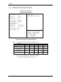
1
GMB-486SG
High Performance
486
VLB Motherboard
User’s Manual
For
GMB-486sg v2
Manual Edition 6.03
This guide contains instructions for configuring and installing the mainboard.
•
Chapter 1, Introduction, acquaints user with the special features of the mainboard.
•
Chapter 2, Hardware Configuration, gives information on configuring memory and setting the
mainboard's jumpers. Brief sections on installing memory.
•
Chapter 3, Mainboard Installation, is an overview of how to install the mainboard in a system.
•
Chapter 4, BIOS Setup, provides the BIOS information for system configuration.
•
Chapter 5, BIOS POST Messages, provides references for all POST error messages.
•
Chapter 6, BIOS Default Drive Table, provides a Default Drive Disk table contained in Setup.
WARNING
For the system to operate normally please make sure JP16 of the mainboard is set as below. Refer to Fig 2 in
this manual for the location JP16.
If JP16 is open, no
CMOS data can be
retained.
The information presented in this publication has been carefully checked for reliability; however, no
responsibility is assumed for inaccuracies, whereas, specification is subjected to change without notice.
All rights reserved. No part of this Manual may be reproduced in any form without the written permission.
i
UNPACKING THE MAINBOARD
The Mainboard comes packed in a sturdy cardboard shipping carton. The carton contains:
•
The Mainboard
•
This User's Guide
Note:
Do not remove the mainboard from its original packing until ready to install.
The mainboard is easily damaged by static electricity. Observe the following precautions while unpacking and
installing the mainboard.
1.
Touch an unpainted area of the system chassis before handling the mainboard or any component.
Doing so, discharges the static charge the user's body may have built.
2.
Remove the mainboard from its anti-static wrapping and place it on a grounded surface, component
side up.
3.
Inspect the mainboard for damage. Shipping may have loosened integrated circuits from their
sockets. If any integrated circuit appears loose, press carefully to seat it firmly in this socket.
Do not apply power if the mainboard appears damaged. If there is damage to the board, or items are missing,
contact dealer immediately.
ii
CONTENTS
CHAPTER 1
1.1
1.2
1.3
INTRODUCTION
KEY FEATURES
MAINBOARD COMPONENTS
VESA LOCAL BUS SPECIAL FEATURES
CHAPTER 2
2.1
2.2
HARDWARE CONFIGURATION
5
JUMPER AND MEMORY BANK LOCATIONS
5
JP8, JP10-JP15, JP21, JP22, JP24, JP25, JP30,
JP31, JP34-JP36, JP38 - CPU TYPE CONFIGURATION
6
CPU INSTALLATION
14
CACHE CONFIGURATION
15
2.4.1
UPGRADING CACHE
15
2.4.2
CACHE SIZE AND MEMORY LOCATIONS
16
2.4.3
CACHE CHIP SOCKETS AND JUMPER LOCATIONS16
2.4.4
JP1-JP4, JP33 - CACHE & TAG RAM JUMPER SETTING 17
2.4.5
INSTALLING CACHE CHIPS
18
JP28, JP29 - VL-BUS IDENTIFY PINS
19
JP16 - CMOS RAM BATTERY SETTING
19
JP17 - MONITOR SETTING
20
JP20 - CPU CLOCK DELAY
20
JP5, JP6, JP7 - CPU FREQUENCY
CONFIGURATION
21
JP37 - FLASH ROM JUMPER
21
MEMORY INSTALLATION
22
2.11.1 INSTALLING SIMM
25
2.3
2.4
2.5
2.6
2.7
2.8
2.9
2.10
2.11
CHAPTER 3
3.1
3.2
3.3
3.4
3.5
CHAPTER 4
4.1
4.2
4.3
4.4
1
1
3
4
MAINBOARD INSTALLATION
COMPONENTS
INSTALLING THE MAINBOARD
CONNECTION THE MAINBOARD
3.3.1
CONNECTION LOCATIONS
CONNECTORS
3.4.1
CN1 - KEYBOARD CONNECTOR
3.4.2
CN2 - POWER SUPPLY CONNECTOR
3.4.3
J1 - EXTERNAL BATTERY
3.4.4
J2 - GREEN POWER SUPPLY CONNECTOR
3.4.5
J3 - TURBO SWITCH CONNECTOR
3.4.6
J4 - TURBO LED CONNECTOR
3.4.7
J5 - SPEAKER CONNECTOR
3.4.8
J6 - RESET SWITCH CONNECTOR
3.4.9
J7 - KEYLOCK & POWER LED CONNECTOR
3.4.10 JP26 - GREEN PC BREAK SWITCH
3.4.11 JP27 - SM_LED CONNECTOR
SYSTEM ASSEMBLY OVERVIEW
27
27
28
28
29
29
29
30
30
31
31
32
32
32
33
33
33
34
AWARD BIOS SETUP
ENTERING SETUP
CONTROL KEYS
GETTING HELP
THE MAIN MENU
4.4.1
STANDARD CMOS SETUP MENU
35
35
36
36
37
38
iii
4.4.2
4.4.3
4.4.4
4.4.5
4.4.6
4.4.7
4.4.8
4.4.9
4.4.10
CHAPTER 5
5.1
5.2
iv
BIOS FEATURES SETUP MENU
CHIPSET FEATURES SETUP MENU
POWER MANAGEMENT SETUP MENU
LOAD BIOS DEFAULTS MENU
LOAD SETUP DEFAULTS MENU
PASSWORD SETTING MENU
IDE HDD AUTO DETECTION MENU
SAVE & EXIT SETUP MENU
EXIT WITHOUT SAVING MENU
BIOS POST MESSAGE
POST BEEP
ERROR MESSAGES
39
40
41
43
43
43
44
44
44
45
45
45
Introduction
CHAPTER 1
INTRODUCTION
The mainboard is a 2/3 body AT size high-performance mainboard that provides with basic elements on which
to build an advanced computer. The mainboard running from 25MHz to 133MHz, supports Normal 486
CPUs, Intel's SL-Enhanced 486, Cyrix Cx486S/DX/DX2, UMC U5SX-486, P24D/P24T; and optionally
support P24C(486DX4), Am486DX2/DX4(3.45V), Enhanced Am486DX2/DX4 (3.45V), Cx486DX2V66/V80, Cyrix DX4-100, Cx5x86-100, TI DX2-80, IBM486-4V3100GC/GIC and AMD-X5-133ADW
CPUs.
1.1
KEY FEATURES
The advanced features of the mainboard include:
• Supports Intel's SL Enhanced 80486DX2/DX/SX,
Cyrix's Cx486S/DX/DX2, UMC U5SX-486, normal 486, P24D/P24T;
and optionally support P24C(486DX4), Am486DX2/DX4(3.45V),
Enhanced Am486DX2/DX4 (3.45V), Cx486DX2-V66/V80, Cyrix
DX4-100, Cx5x86-100, TI DX2-80, IBM 486-4V3100GC/GIC and
AMD-X5-133ADW CPUs.
• Supports Cache Write back CPU (P24T/P24D/Cx486S/DX/DX2/DX2V),
and Enhanced Am486DX2/DX4, Cyrix DX4/5x86, IBM 486 and
AMD-X5 CPUs.
• 100% IBM PC-AT compatible, single chips 486 solution.
• Provides power saving features to allow a system, through the control of
BIOS, to reduce the CPU clock frequency down to 0MHz
(STOP CLOCK) when the system is idle.
• Supports Power Management Mode
- Supports the SMM and the SMI
- CPU Stop Clock Function
- Long and Short System Timers
- Supports the APM control
- Supports Break Switch control
- Power Saving also on non-SMI CPU
- More System Event Monitoring and the Power saving Control
• Direct Mapped Cache Controller
- Write-Back or Write-Through Schemes
- Bank Interleave or Non-Interleave Cache
- Flexible Cache Size: 128/256/512KB
• Memory size from 1MB to 128MB, possible using combinations of
1M, 2M, 4M, 8M, 16M, 32M, or 64M 72-pin SIMM modules in
four memory banks.
• Easy upgrade the system, just change CPU, or and alter jumper only.
• System & video Bios Shadow, optional caching of shadowed system &
video BIOS.
1
Chapter 1
• Hidden DRAM refresh support.
• Support KB control Turbo/Deturbo mode select.
• Support 7 Direct Memory Access channels and 16 Interrupt levels.
• Three 16-bit I/O slots, one 8-bit I/O slots, and three Standard VESA
Local Bus master slot.
• Battery backup for CMOS configuration and real time clock/calendar.
• 8MHz AT Bus clock & speed changeable by hardware or keyboard, CPU
clock adjustable by jumper.
• 2/3 Baby AT board size = 220mm(W) X 250mm(L).
2
Introduction
1.2
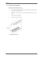
MAINBOARD COMPONENTS
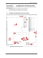
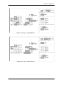
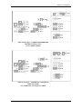
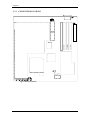
This section gives a brief description of key components on the mainboard. Refer to Fig 1 for
component locations.
Fig 1 Key Components of the Mainboard
3
Chapter 1
1.3
VESA LOCAL BUS SPECIAL FEATURES
• Three-bus master are supported on the VESA Local-Bus. The VESA Local-Bus connector type is a
standard 32-bit Micro Channel type connector, and is located inline with a system I/O bus connector.
• Three slots are provided on the mainboard. Either with one master or three master slots.
• The VESA Local-Bus can support high speed video controllers, and other peripherals, such as hard
disk controllers, LAN adapters, and so on.
• Interface protocol depends on the CPU speed, but protocol selection and switching is invisible to all
add-in boards, software, and end users. The VESA Local-Bus always remains totally transparent to
all application software.
• 32-bits optimum data bus width
4
Hardware Configuration
CHAPTER 2
HARDWARE CONFIGURATION
This chapter describes how to set the mainboard jumpers for cache memory and display type, and how to
install memory modules.
Before beginning the configuration, user should take the following precautions:
•
Turn off the power supply, and unplug the power cord before begin.
•
Unplug all cables that connect the mainboard to any external devices.
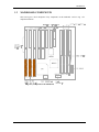
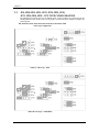
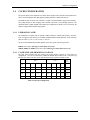
2.1
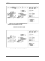
JUMPER AND MEMORY BANK LOCATIONS
Fig 2 Jumper and Memory Bank Locations
5
Chapter 2
2.2
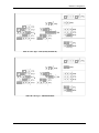
JP8, JP10-JP15, JP21, JP22, JP24, JP25, JP30,
JP31, JP34-JP36, JP38 - CPU TYPE CONFIGURATION
The mainboard can support processor at different speed. Various jumpers are required to setup for
installing different CPU. Refer to Fig 2 for the jumpers’ location, and set the jumper according to the
following table:
JP8, JP10-JP15, JP21, JP22, JP24, JP25, JP30, JP31, JP34-JP36, JP38
--CPU Type Configuration
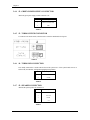
Table 1A: CPU Type: - P24T
Table 1B: CPU Type: - P24D (DX2)
6
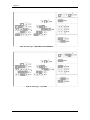
Hardware Configuration
Table 1C: CPU Type: - P24C (DX4) (OPTIONAL)
Table 1D: CPU Type: - 486SX/SLE 486SX
7
Chapter 2
Table 1E: CPU Type: - 486DX/DX2, SLE 486DX/DX2
Table 1F: CPU Type: - Cyrix 486S
8
Hardware Configuration
Table 1G: CPU Type: - Cyrix 486DX/DX2
Table 1H: CPU Type: - UMC U5SX-486
9
Chapter 2
Table 1I: CPU Type: - Enhanced Am486DX2/DX4 (3.45V)
(A80486DX2-XXSV8B/A80486DX4-1XXSV8B)
For DX4-100 CPU Frequency: 33MHz
For DX4-120 CPU Frequency: 40MHz
Table 1J: CPU Type: - Am486DX2 (3.45V) (Optional)
10
Hardware Configuration
Table 1K: CPU Type: - Am486DX4 (3.45V) (Optional)
Table 1L: CPU Type: - Cx486DX2-V66 (3.6V) (Optional)
11
Chapter 2
Table 1M: CPU Type: - Cx486DX2-V80 (4.0V) (Optional)
Table 1N: CPU Type: - Cx5x86/IBM 486-4V3100GIC (3.3V)
12
Hardware Configuration
Table 1O: CPU Type: - Cx486DX4-100/TI486DX2-80/
IBM 486-4V3100GC (3.45V)
(Cyrix Cx486DX4-100GP)
Table 1P: CPU Type: - Am5x86 -P75 (3.45)(Optional)
(AMD-X5-133ADW)
For 133MHz CPU, CPU Frequency: 33MHz
13
Chapter 2
Table 1Q: CPU Type: - P24D (DX4)
2.3
CPU INSTALLATION
The mainboard has a socket that can support 486 CPU. See Fig 1 in Chapter 1 for the socket's
location.
Install the 486 CPU as follows:
Caution: Static electricity can damage the processor.
1.
Plug the 486 CPU into the socket, with the notch corner aligned.
Fig 3 Installing a CPU
2.
14
Change the CPU type jumper setting according to the CPU Jumper Setting table on the
previous pages.
Hardware Configuration
2.4
CACHE CONFIGURATION
The special feature of the mainboard is a built-in direct-mapped cache controller with optional writeback or write-through operation that supports 128KB, 256KB or 512KB cache memory.
The mainboard has a built-in cache controller. It requires external SRAM as tag and cache memory.
The caching Scheme is direct mapping with selectable write-back or write-through operation. The
mainboard allows 128KB, 256KB, and 512KB cache configurations. Memory size is selected by the
hardware jumpers and the BIOS setup program.
2.4.1
UPGRADING CACHE
The mainboard is available with an optional 128KB, 256KB or 512KB cache memory on-board.
User can upgrade cache memory by installing additional SRAM (Static Random Access Memory)
chips in sockets U1, U2, U3, U4, U5, U6, U7, U8; U11.
The speed of the SRAM chips needed depends on the clock speed of the microprocessor:
25MHz clock requires 25ns (tag) and 25ns (data) SRAM chips.
33MHz, 40MHz, or 50MHz clock CPU requires 20ns (tag) and 20ns (data) SRAM chips.
2.4.2
CACHE SIZE AND MEMORY LOCATIONS
The table below describes the chip capacity and socket location required for each cache size
configuration. User can use 32Kx8-bit or 128Kx8-bit SRAM chips in banks 0 and 1, and in the Tag
RAM socket. Please note that; do not combine different chip capacities in banks 0 and 1.
BANK 0
BANK 1
TAG
RAM
Cache
Size
U1
U2
U3
U4
U5
U6
U7
U8
U11
128K
32Kx8
32Kx8
32Kx8
32Kx8
NONE
NONE
NONE
NONE
8Kx8
256K
32Kx8
32Kx8
32Kx8
32Kx8
32Kx8
32Kx8
32Kx8
32Kx8
16Kx8/
32Kx8
256K
64Kx8
64Kx8
64Kx8
64Kx8
NONE
NONE
NONE
NONE
16Kx8/
32Kx8
512K
128Kx8
128Kx8
128Kx8
128Kx8
NONE
NONE
NONE
NONE
32Kx8
Table 2: Cache Size Configuration
15
Chapter 2
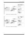
2.4.3
CACHE CHIP SOCKETS AND JUMPER LOCATIONS
The diagram below describes the location of the cache chip sockets and cache jumpers.
Fig 4 Cache Jumper and Socket Locatio
16
Hardware Configuration
2.4.4
JP1-JP4, JP33 - CACHE & TAG RAM JUMPER SETTING
Cache memory is configured using jumpers, JP1, JP3, & JP33; while Tag RAM setting is configured
using jumpers JP2, JP4. The following tables summarize the possible configuration.
JP1, JP3, JP33 -- Cache Jumper Setting
Table 3A: Cache Jumper Setting
JP2, JP4 -- Tag RAM Jumper Setting
Table 3B: Tag RAM Jumper Sett
Note:
D = Double Bank;
S = Single Bank
17
Chapter 2
2.4.5
INSTALLING CACHE CHIPS
Install cache chips on the mainboard as follows:
Caution: Static electricity can damage a cache chip.
1.
Review the section on static electricity precautions at the beginning of this manual, and make
sure that power to the mainboard is off.
2.
Align the chip so that the notched corner of the chip matches the notched corner of the
socket.
3.
Align the pins with the socket holes.
4.
Carefully press the chip into the socket.
Fig 5 Installing a Cache Chip
18
Hardware Configuration
2.5
JP28, JP29 - VL-BUS IDENTIFY PINS
Set the jumpers, JP28 & JP29 to configure the VL-Bus Clock Speed. Refer to Fig 2 for their location.
Set the jumper as below.
JP28, JP29 -- VL-Bus Clock Speed
Table 4
2.6
JP16 - CMOS RAM BATTERY SETTING
Please set JP16 is for CMOS RAM battery as below. Refer to Fig 2 for the location of JP16.
JP16 -- CMOS RAM Battery Setting
Table 5
2.7
JP17 - MONITOR SETTING
Set the jumper, JP17, to configure the mainboard for either CGA, monochrome, OR VGA/EGA
display. Refer to Fig 2 for the location of JP17. Set the jumper as below.
JP17 -- Monitor Setting
Table 6
19
Chapter 2
2.8
JP20 - CPU CLOCK DELAY
JP20 is for the CPU Clock Delay setting. Refer to Fig 2 for JP20 location.
JP20 -- CPU Clock Delay
Table 7
2.9
JP5, JP6, JP7 - CPU FREQUENCY CONFIGURATION
JP5, JP6, & JP7 are for the CPU Frequency Configuration. Two different settings are provided for
different Clock Generator that is used at U16 or U17. Refer to Fig 2 for the location of U16/U17 and
jumpers.
JP5, JP6, JP7-- CPU Frequency Configuration
Table 8
Note:
20
Winbond W83C17 and UMC U59515-01 are pin to pin compatible to MX-8315 and
PhaseLink PLL52C08-01 is pin to pin compatible to AV9107-03.
Hardware Configuration
2.10 JP37 - FLASH ROM JUMPER
JP37 is for Flash ROM selection. Refer to Fig 2 for its location.
JP37 -- Flash ROM Jumpers
Table 9
21
Chapter 2
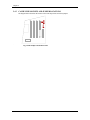
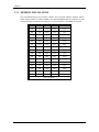
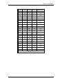
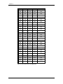
2.11 MEMORY INSTALLATION
Four 72pin SIMM sockets are provided in 4 Banks. User can install 256Kx36, 512Kx36, 1Mx36,
2Mx36, 4Mx36, 8Mx36, or 16Mx36 SIMMs. Note that all SIMM modules in a bank must be same
capacity and follow combination showed below. For best performance 70ns SIMMs are required.
BANK 0
BANK 1
BANK 2
BANK 3
MEMORY SIZE
1MB
NONE
NONE
NONE
1MB
1MB
1MB
NONE
NONE
2MB
2MB
NONE
NONE
NONE
2MB
1MB
1MB
2MB
NONE
4MB
2MB
2MB
NONE
NONE
4MB
4MB
NONE
NONE
NONE
4MB
1MB
4MB
NONE
NONE
5MB
1MB
1MB
4MB
NONE
6MB
2MB
4MB
NONE
NONE
6MB
1MB
1MB
2MB
4MB
8MB
2MB
2MB
4MB
NONE
8MB
4MB
4MB
NONE
NONE
8MB
8MB
NONE
NONE
NONE
8MB
1MB
1MB
4MB
4MB
10MB
2MB
2MB
4MB
4MB
12MB
4MB
4MB
4MB
NONE
12MB
TO BE CONTINUED ...
22
Hardware Configuration
BANK 0
BANK 1
BANK 2
BANK 3
MEMORY SIZE
4MB
8MB
NONE
NONE
12MB
4MB
4MB
4MB
4MB
16MB
8MB
8MB
NONE
NONE
16MB
16MB
NONE
NONE
NONE
16MB
4MB
4MB
8MB
NONE
16MB
1MB
16MB
NONE
NONE
17MB
1MB
1MB
16MB
NONE
18MB
2MB
16MB
NONE
NONE
18MB
2MB
2MB
16MB
NONE
20MB
4MB
16MB
NONE
NONE
20MB
4MB
8MB
8MB
NONE
20MB
2MB
2MB
4MB
16MB
24MB
4MB
4MB
16MB
NONE
24MB
8MB
8MB
8MB
NONE
24MB
4MB
4MB
8MB
8MB
24MB
8MB
16MB
NONE
NONE
24MB
4MB
8MB
8MB
8MB
28MB
16MB
16MB
NONE
NONE
32MB
32MB
NONE
NONE
NONE
32MB
8MB
8MB
16MB
NONE
32MB
8MB
8MB
8MB
8MB
32MB
TO BE CONTINUED ...
23
Chapter 2
BANK 0
BANK 1
BANK 2
BANK 3
MEMORY SIZE
2MB
2MB
16MB
16MB
36MB
4MB
16MB
16MB
NONE
36MB
4MB
32MB
NONE
NONE
36MB
4MB
4MB
16MB
16MB
40MB
4MB
4MB
32MB
NONE
40MB
8MB
8MB
8MB
16MB
40MB
16MB
16MB
16MB
NONE
48MB
16MB
32MB
NONE
NONE
48MB
8MB
8MB
16MB
16MB
48MB
8MB
8MB
32MB
NONE
48MB
16MB
16MB
16MB
16MB
64MB
64MB
NONE
NONE
NONE
64MB
16MB
16MB
32MB
NONE
64MB
32MB
32MB
NONE
NONE
64MB
1MB
64MB
NONE
NONE
65MB
4MB
64MB
NONE
NONE
68MB
4MB
32MB
32MB
NONE
68MB
4MB
4MB
64MB
NONE
72MB
4MB
4MB
32MB
32MB
72MB
16MB
64MB
NONE
NONE
80MB
16MB
32MB
32MB
NONE
80MB
8MB
8MB
32MB
32MB
80MB
16MB
16MB
64MB
NONE
96MB
16MB
16MB
32MB
32MB
96MB
32MB
32MB
32MB
NONE
96MB
64MB
64MB
NONE
NONE
128MB
32MB
32MB
32MB
32MB
128MB
Table 10: On-board Memory Configuration
24
Hardware Configuration
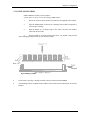
2.11.1 INSTALLING SIMM
Install a SIMM in a memory socket as follows:
Caution: Static electricity can seriously damage SIMM modules.
1.
Review the section on static electricity precautions at the beginning of this manual.
2.
Align the SIMM module so that the pin-1 marking on the module corresponds to
the socket pin-1 marking.
3.
Hold the module at a 70-degree angle to the socket, and insert the module's
connectors into the socket.
4.
Snap the module to a vertical position in the socket. The module is fully inserted
when retaining pegs snap into holes at each end of the module.
Fig 6 Installing a SIMM
5.
To fill a bank, repeat steps 1 through 4 until the sockets in each bank contain SIMMs.
6.
After installing memory, run BIOS Setup to indicate to the system for how much memory the user has
installed.
25
Chapter 3
CHAPTER 3
MAINBOARD INSTALLATION
Once the mainboard's hardware has been configured, the user is now ready to install the mainboard into the
system chassis. This chapter describes what are needed to assemble an advanced computer system based on
the mainboard.
3.1
COMPONENTS
The following components are recommended:
26
•
Case with standard chassis and hardware. The mainboard fits most AT compatible cases.
•
Standard AT power supply.
•
8 ohm speaker.
•
Floppy disk drive(s) (360KB, 1.2MB, or 1.44MB).
•
Hard disk drive (optional).
•
Hard disk and floppy disk drive controller card.
•
Flat ribbon cables to connect the disk drive controller and the disk drive(s).
•
Serial/parallel interface card.
•
AT-compatible keyboard.
•
Video card and Display (monochrome, CGA, EGA, or VGA).
Mainboard Installation
3.2
INSTALLING THE MAINBOARD
Before starting, check the location of the mounting holes in the case and on the mainboard.
Caution: Static electricity can damage the mainboard.
Install the mainboard as follows:
1.
Review the section on static electricity precautions at the beginning of this manual.
2.
Place the case on an anti-static mat and remove the cover. Remove the nylon stand-offs and
screws for mounting the mainboard.
3.
Put the front of the case to the right and the rear to the left. The mainboard occupies the
section of the case nearest the user; the power supply goes on the far side.
4.
Align the mounting holes on the case to the mounting holes on the mainboard. Make sure to
access the keyboard connector once the board is installed.
5.
From the bottom of the mainboard, insert stand-offs into the proper holes on the board, and
attach the mounting screws to the bottom of the case.
Note: Some cases do not use stand-offs and mounting screws; in this case user can fasten the
mainboard into the case with regular screws.
6.
Place the mainboard into the case and fasten the board securely with regular screws.
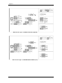
3.3
CONNECTION THE MAINBOARD
Once the mainboard has been fastened into the system case, the next step is to connect the internal
cables. The internal cables are wire leads with plastic female connectors that attach to the connectors.
The mainboard connectors have varying numbers of pins and are the points of contact between the
mainboard and other parts of the computer.
A description of each connector and its connector pins follows. See Fig 7 for the location of the
connectors on the mainboard.
Note: Before making connectors on the board, make sure that power to the system is turned off.
27
Chapter 3
3.3.1
CONNECTIONLOCATIONS
Fig 7 Connector Locations
28
Mainboard Installation
3.4
CONNECTORS
3.4.1
CN1 - KEYBOARD CONNECTOR
A standard five-pin female DIM keyboard connector is located at the rear of the keyboard. Plug the
jack on the keyboard cable into this connector.
Pin
Description
1
Keyboard Clock
2
Keyboard Data
3
Spare
4
Ground
5
+5V DC
Table 11
3.4.2
CN2 - POWER SUPPLY CONNECTOR
The power supply connector has twelve-pin male header connectors. Plug the dual connectors from
the power directly onto the board connector.
CN2
Pin
Description
Pin
Description
1
Power Good
7
Ground
2
+5V DC
8
Ground
3
+12V DC
9
-5V DC
4
-12V DC
10
+5V DC
5
Ground
11
+5V DC
6
Ground
12
+5V DC
Table 12
3.4.3
J1 - EXTERNAL BATTERY
The mainboard has a battery on-board; however, user can also attach an external battery to connector
J1. Using an external battery helps to conserve the on-board battery.
Pin
Description
1
VDD (6V)
2
Not Used
3
Ground
4
Ground
Table 13
29
Chapter 3
3.4.4
J2 - GREEN POWER SUPPLY CONNECTOR
Attach the green power supply control connector to J2.
Pin
Description
1
Pull Low on Power Down
2
GND
Table 14
3.4.5
J3 - TURBO SWITCH CONNECTOR
J3 connects to the Turbo switch, which is used to select the mainboard's clock speed.
Table 15
3.4.6
J4 - TURBO LED CONNECTOR
J4 is usually connected to a Turbo LED on front of the system case. If the system board select is in
Turbo mode, the indicator will light during high-speed operation.
Pin
Description
1
- Cathode
2
+ Anode
Table 16
3.4.7
J5 - SPEAKER CONNECTOR
Attached the system speaker to connector J5.
Pin
Description
1
Data Out
2
Not Used
3
Ground
4
+ 5V
Table 17
30
Mainboard Installation
3.4.8
J6 - RESET SWITCH CONNECTOR
Attach the Reset switch cable to this connector. The Reset switch restarts the system.
Setting
Description
Close
Reset
Open
Normal
Table 18
3.4.9
J7 - KEYLOCK & POWER LED CONNECTOR
J7 is a keylock connector that enables and disables the keyboard and the Power-LED on the case.
Pin
Description
1
LED Power
2
Not Used
3
Ground
4
Keyboard Inhibitor
5
Ground
Table 19
3.4.10 JP26 - GREEN PC BREAK SWITCH
JP26 is for the Green feature activation Break Switch. When JP26 is changed from open to
close then open again, the system will go to suspend mode immediately. In suspend mode; if
JP26 is changed from open to close then open again, the system will resume immediately.
3.4.11 JP27 - SM_LED CONNECTOR
JP27 is used for Power Management Mode. If the system operate in Power Management
Mode, the indicator will turn on during the mode.
Pin
Description
1
+ Anode
2
- Cathode
Table 20
31
Chapter 3
3.5
SYSTEM ASSEMBLY OVERVIEW
After installing and connecting the mainboard, assemble components in the following order:
1.
Power Supply: Place the power supply so that it fits the raised tongues on the chassis floor.
Insert and fasten the two screws on the back panel of the chassis. Connect the power supply
to the power supply connector.
2.
Disk Drives: Slide disk drives into the chassis. Connect a wide 34-wire ribbon cable to each
disk drive; this cable will attach to an adapter card. The power supply has four cables, each
with four wires. Connect these cables to the disk drives.
3.
Adapter Cards: Insert each adapter card -- Disk Controller cards, Video card,
Serial/Parallel Interface card, etc. -- into an expansion slot. Refer to the installation and
configuration instructions that comes with the card. Connect the disk drives to the Floppy
Disk and Hard Disk Controller cards.
4.
Keyboard: Connect the keyboard to its connector.
5.
Display: Connect the display cable to the Video Card, and the display's power cord into a
power outlet.
6.
Case: Slide on the case cover and fasten its screws.
Connect the power cord to the power supply and plug it into a wall outlet. Put the boot disk into drive
A: and turn on the power. User will then need to run the BIOS setup program.
32
Award BIOS Setup
CHAPTER 4 AWARD BIOS SETUP
Award's BIOS ROM has a built-in Setup program that allows users to modify the basic system configuration.
This type of information is stored in battery-backed RAM so that it retains the Setup information when the
power is turned off.
4.1
ENTERING SETUP
Power on the computer and press <Del> immediately will allow you to enter Setup. The other way to
enter Setup is to power on the computer, when the below message appears briefly at the bottom of the
screen during the POST (Power On Self Test), press <Del> key or simultaneously press <Ctrl>,
<Alt>, and <Esc> keys.
TO ENTER SETUP BEFORE BOOT PRESS CTRL-ALT-ESC OR
DEL KEY
If the message disappears before you respond and you still wish to enter Setup, restart the system to
try again by turning it OFF then ON or pressing the "RESET" button on the system case. You may
also restart by simultaneously press <Ctrl>, <Alt>, and <Delete> keys. If you do not press the keys at
the correct time and the system does not boot, an error message will be displayed and you will again
be asked to,
PRESS F1 TO CONTINUE, CTRL-ALT-ESC OR DEL TO
ENTER SETUP
33
Chapter 4
4.2
CONTROL KEYS
Move to previous item
Up arrow:
Move to next item
Down arrow:
Move to the item in the left hand
Left arrow:
Move to the item in the right hand
Right arrow:
Esc key: Main Menu -- Quit and not save changes into CMOS
Status Page Setup Menu and Option Page Setup Menu -- Exit current page and
return to Main Menu
Increase the numeric value or make changes
PgUp key:
Decrease the numeric value or make changes
PgDn key:
F1 key: General help, only for Status Page Setup Menu and Option Page Setup Menu
F2 key: Change colour from total 16 colors
F3 key: Calendar, only for Status Page Setup Menu
F4 key: Reserved
F5 key: Restore the previous CMOS value from CMOS, only for Option Page Setup Menu
F6 key: Load the default CMOS value from BIOS default table, only for Option Page Setup Menu
F7 key: Load the default
F8 key: Reserved
F9 key: Reserved
F10 key:Save all the CMOS changes, only for Main Menu
4.3
GETTING HELP
Main Menu:
The on-line description of the highlighted setup function is displayed at the bottom of the screen.
Status Page Setup Menu/Option Page Setup Menu:
Press F1 to pop up a small help window that describes the appropriate keys to use and the possible
selections for the highlighted item. To exit the Help window press <Esc>.
34
Award BIOS Setup
4.4
THE MAIN MENU
Once you enter Award BIOS CMOS Setup Utility, the Main Menu will appear on the screen. The
Main Menu allows you to select from ten setup functions and two exit choices. Use arrow keys to
select among the items and press <Enter> to accept or enter the sub-menu.
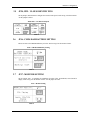
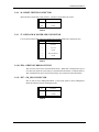
ROM ISA BIOS (2C4I9G30)
CMOS SETUP UTILITY
AWARD SOFTWARE, INC.
STANDARD CMOS SETUP
PASSWORD SETTING
BIOS FEATURES SETUP
IDE HDD AUTO DETECTION
CHIPSET FEATURES SETUP
SAVE & EXIT SETUP
POWER MANAGEMENT SETUP
EXIT WITHOUT SAVING
LOAD BIOS DEFAULTS
LOAD SETUP DEFAULTS
Esc : Quit
F10 : Save & Exit Setup
: Select Item
(Shift)F2 : Change Color
{Description}
Fig 8
35
Chapter 4
4.4.1
STANDARD CMOS SETUP MENU
The items on Standard CMOS Setup Menu are divided into 10 categories. Each category includes no,
one or more than one setup items. Use the arrow keys to highlight the item and then use the <PgUp>
or <PgDn> keys to select the value you want in each item.
ROM ISA BIOS (2C4I9G30)
STANDARD CMOS UTILITY
AWARD SOFTWARE, INC.
Date (mm:dd:yy) : Thu, Mar 3 1994
Time (hh:mm:ss) : 11 : 23 : 53
Drive C : None ( 0Mb)
Drive D : None ( 0Mb)
0
0
CYLS. HEADS PRECOMP LANDZONE SECTORS MODE
0
0
0
0
---0
0
0
0
----
Drive A: 1.44M, 3.5in.
Drive B : None
Video : EGA/VGA
Base Memory:
Extended Memory:
Expanded Memory:
Other Memory:
640K
3072K
0K
384K
Halt On : All Errors
Total Memory:
4096K
Esc : Quit
F1 : Help
: Select Item
(Shift)F2 : Change Color
Fig 9
36
PU/PD/+/- : Modify
Award BIOS Setup
4.4.2
BIOS FEATURES SETUP MENU
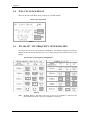
ROM ISA BIOS (2C4I9G30)
BIOS FEATURES SETUP
AWARD SOFTWARE, INC.
Virus Warning
: Enabled
CPU Internal Cache
: Enabled
External Cache
: Enabled
Quick Power On Self Test : Enabled
Boot Sequence
: C,A
Swap Floppy Drive
: Disabled
Boot Up Floppy Seek
: Disabled
Boot Up Numlock Status : On
Boot Up System Speed
: High
IDE HDD Block Mode
: Disabled
Gate A20 Option : Fast
Typematic Rate Setting : Disabled
Typematic Rate (Chars/Sec): 6
Typematic Delay (Msec) : 250
Security Option
: Setup
Video BIOS Shadow : Enabled
C8000-CFFFF Shadow: Disabled
D0000-D7FFF Shadow: Disabled
D8000-DFFFF Shadow: Disabled
E0000-E7FFF Shadow : Disabled
E8000-EFFFF Shadow: Disabled
ESC: Quit
: Select Item
F1: Help
PU/PD/+/-: Modify
F5: Old Values (Shift)F2: Color
F6: Load BIOS Defaults
F7: Load Setup Defaults
Fig 10
37
Chapter 4
4.4.3
CHIPSET FEATURES SETUP MENU
ROM ISA BIOS (2C4I9G30)
CHIPSET FEATURES SETUP
AWARD SOFTWARE, INC.
Latch Local Bus
Local Bus Ready
Auto Configuration : Enabled
AT Bus Clock
Hidden Refresh
: 1/5CLK
: Enable
L2 Cache Scheme
L1 Cache Scheme
Cache Burst Read
Cache Write Cycle
System Shadow
Video Shadow
: Write Back
: Write Back
: 2T
: 3T
: Non-Cacheable
: Non-Cacheable
: T3
: Synchronize
Fast Reset Emulation: Enable
Fast Reset Latency : 2 us
ESC: Quit
: Select Item
F1: Help
PU/PD/+/-: Modify
F5: Old Values (Shift)F2: Color
F6: Load BIOS Defaults
F7: Load Setup Defaults
Fig 11: Default Setting for Cx486DX 40MHz CPU
Note:
1) the following table shows the settings for different CPU
Support: System Clock Freq.
20MHz
25MHz
33MHz
40MHz
50MHz
CPU Internal Clock Freq.
x1
x1/x2/x3
x1/x2/x3
x1/x2
x1
AT Bus Clock
1/3CLK
1/3CLK
1/4CLK
1/5CLK
1/6CLK
Cache Burst Read
1T
1T
2T
2T
2T
Cache Burst Write
2T
2T
2T
3T
3T
2) The option "L1 Cache Scheme" is shown only when the
Cyrix Cx486S/Cx486DX/DX2 CPUs are used.
38
Award BIOS Setup
4.4.4 POWER MANAGEMENT SETUP MENU
ROM ISA BIOS (2C4I9G30)
POWER MANAGEMENT SETUP
AWARD SOFTWARE, INC.
Power Management : Max Saving
PM Control by APM
: Yes
VGA Adapter Type: Non-Green
Video Off Option
: Always On
** PM Timers **
HDD Power Down : Disable
System Suspend
: 10 Sec
** PM Events **
Local Master
: Disable
Local Device
: Disable
Video Activities
: Disable
DMA Activities
: Enable
IRQ 1 (Keyboard) : Enable
IRQ 3 (COM 2)
: Enable
IRQ 4 (COM 1)
IRQ 5 (LPT or LAN)
IRQ 6 (Floppy Disk)
IRQ 7 (LPT or LAN)
IRQ 8 (RTC, OS2) : Disable
IRQ 9 (Reserved)
IRQ 10 (Reserved) : Enable
IRQ 11 (Reserved) : Enable
IRQ 12 (PS2 mouse)
IRQ 13 (387)
IRQ 14 (Hard Disk) : Enable
IRQ 15 (Reserved) : Enable
: Enable
: Enable
: Enable
: Enable
: Enable
: Enable
: Enable
ESC: Quit
: Select Item
F1: Help
PU/PD/+/-: Modify
F5: Old Values (Shift)F2: Color
F6: Load BIOS Defaults
F7: Load Setup Defaults
Fig 12A SL Enhanced 486 CPU
39
Chapter 4
ROM ISA BIOS (2C4I9G30)
POWER MANAGEMENT SETUP
AWARD SOFTWARE, INC.
Power Management : Max Saving
PM Control by APM
: Yes
VGA Adapter Type: Non-Green
Video Off Option
: Always On
PM Mode
: Via IRQ12
** PM Timers **
HDD Power Down : Disable
System Suspend
: 10 Sec
IRQ 4 (COM 1)
IRQ 5 (LPT or LAN)
IRQ 6 (Floppy Disk)
IRQ 7 (LPT or LAN)
IRQ 8 (RTC, OS2) : Disable
IRQ 9 (Reserved)
IRQ 10 (Reserved) : Enable
IRQ 11 (Reserved) : Enable
IRQ 12 (PS2 mouse)
IRQ 13 (387)
IRQ 14 (Hard Disk) : Enable
: Enable
: Enable
: Enable
: Enable
: Enable
: Enable
: Enable
** PM Events **
Local Master
: Disable
Local Device
: Disable
Video Activities
: Disable
DMA Activities
: Enable
IRQ 1 (Keyboard) : Enable
IRQ 3 (COM 2)
: Enable
ESC: Quit
: Select Item
F1: Help
PU/PD/+/-: Modify
F5: Old Values (Shift)F2: Color
F6: Load BIOS Defaults
F7: Load Setup Defaults
Fig 12B Normal 486 CPU
Note:
1.
2.
40
If the CPU does not belong to Intel S-series, Enhanced Am486DX or Cx486S/S2/DX/DX2,
the system will support IRQ service. When you do not use MS-DOS as the operating system
please set "Power Management" to Disable, because IRQ mode only support MS-DOS.
If CPU belongs to Intel S-series, Enhanced Am486DX or Cx486S/S2/DX/DX2, the system
will support SMI feature. It can support many operating system, such as MS-DOS, OS/2,
Windows NT, etc.
Award BIOS Setup
4.4.5
LOAD BIOS DEFAULTS MENU
When you select this function, the following message will appear at the centre of the screen to assist
you to load BIOS defaults (except Standard CMOS Setup).
Load BIOS Defaults (Y/N)?
4.4.6
LOAD SETUP DEFAULTS MENU
When you select this function, the following message will appear at the centre of the screen to assist
you to load Setup defaults (except Standard CMOS Setup).
Load SETUP Defaults (Y/N)?
4.4.7
PASSWORD SETTING MENU
When you select this function, the following message will appear at the centre of the screen to assist
you in creating a password.
ENTER PASSWORD:
Type the password, up to eight characters, and press <enter>. The password typed now will clear any
previously entered password from CMOS memory. You will be asked to confirm the password.
Type the password again and press <Enter>. You may also press <Esc> to abort the selection and not
enter a password.
To disable password, just press <Enter> when you are prompted to enter password. A message will
confirm the password being disabled. Once the password is disabled, the system will boot and you
can enter Setup freely.
PASSWORD DISABLED.
If you select System at Security Option of BIOS Features setup Menu; you will be prompted for
password every time the system is rebooted or any time you try to enter Setup. If you select setup at
Security Option of BIOS Features Setup Menu, you will be prompted only when you try to enter
Setup.
41
Chapter 4
4.4.8
IDE HDD AUTO DETECTION MENU
This function will automatically detect the information of the Hard Disk, and list them for your
reference.
ROM ISA BIOS (2C4I9G30)
CMOS SETUP UTILITY
AWARD SOFTWARE, INC.
CYLS. HEADS PRECOMP LANDZONE SECTORS
Drive C : (
Mb)
Select Drive C Option (N=Skip) : N
OPTIONS SIZE CYLS. HEADS PRECOMP LANDZONE SECTORS MODE
1(Y) 81 903
4
65535
902
46
NORMAL
ESC : Skip
Fig 13
The BIOS support 3 HDD Mode, NORMAL, LBA & LARGE. NORMAL mode has the maximum
528MB HDD size; LBA (Logical Block Addressing) mode has the maximum 8.4GB HDD size;
whereas LARGE mode has the maximum 1GB HDD size.
4.4.9
SAVE & EXIT SETUP MENU
When you select this function, the following message will appear at the centre of the screen to assist
you to Save data to CMOS and Exit the Setup.
SAVE to CMOS and EXIT (Y/N)?
4.4.10 EXIT WITHOUT SAVING MENU
When you select this function, the following message will appear at the centre of the screen
to assist you to Abandon all Data and Exit Setup.
Quit Without Saving (Y/N)?
42
BIOS POST Message
CHAPTER 5 BIOS POST MESSAGE
When the BIOS encounters an error that requires the user to correct something, either a beep code will sound
or a message will be displayed in a box in the middle of the screen and the message PRESS F1 TO
CONTINUE, CTRL-ALT-ESC OR DEL TO ENTER SETUP will be shown in the information box at the
bottom.
5.1
POST BEEP
Currently there is only one beep code in BIOS. This code indicates that a video error has occurred
and the BIOS cannot initialize the video screen to display any additional information. This beep code
consists of a single long beep followed by two short beeps.
5.2
ERROR MESSAGES
One or more of the following messages may be displayed if the BIOS detects an error during the
POST. This list includes message for both the ISA and the EISA BIOS.
CMOS BATTERY HAS FAILED:
CMOS battery is no longer functional. It should be replaced.
CMOS CHECKSUM ERROR:
Checksum of CMOS is incorrect. This can indicate that CMOS has become corrupt. A weak battery
may have caused this error. Check the battery and replace if necessary.
DISK BOOT FAILURE, INSERT SYSTEM DISK AND PRESS ENTER:
No boot device was found. Insert a system disk into Drive A: and press <Enter>. If you assumed the system
would boot from hard drive, make sure the controller is inserted correctly and all cables are properly attached.
Also be sure the disk is formatted as a boot device. Then reboot the system.
DISKETTE DRIVES OR TYPES MISMATCH ERROR - RUN SETUP:
Type of diskette drive installed in the system is different from the CMOS definition. Run Setup to reconfigure
the drive type correctly.
DISPLAY SWITCH IS SET INCORRECTLY:
Display switch on the motherboard can be set to either monochrome or color. This indicates the switch is set to
a different setting than indicated in Setup. Determine which setting is correct, and then either turn off the
system and change the jumper, or enter Setup and change the VIDEO selection.
DISPLAY TYPE HAS CHANGE SINCE LAST BOOT:
Since last powering off the system, the display adapter has been changes. You must configure the system for
the new display type.
EISA Configuration Checksum Error
PLEASE RUN EISA CONFIGURATION UTILITY:
The EISA non-volatile RAM checksum is incorrect or cannot correctly read the EISA slot. This can indicate
either the EISA non-volatile memory has become corrupt or the slot has configured incorrectly. Also be sure
the card is installed firmly in the slot.
EISA Configuration Is Not Complete
PLEASE RUN EISA CONFIGURATION UTILITY:
The slot configuration information stored in EISA non-volatile memory is incomplete.
43
Chapter 5
*** NOTE:
When either of these errors appear, the system will boot in ISA mode, which allows you to
run the EISA Configuration Utility.
ERROR ENCOUNTERED INITIALIZING HARD DRIVE:
Hard drive cannot be initialized. Be sure the adapter is installed correctly and all cables are correctly and
firmly attached. Also be sure the correct hard drive type is selected in Setup.
ERROR INITIALIZING HARD DISK CONTROLLER:
Cannot initialize controller. Make sure the cord is correctly and firmly installed in the bus. Be sure the correct
hard drive type is selected in Setup. Also check to see if any jumper needs to be set correctly on the hard drive.
FLOPPY DISK CNTRLR ERROR OR NO CNTRLR PRESENT:
Cannot find or initialize the floppy drive controller. Make sure the controller is installed correctly and firmly.
If there is no floppy drives installed, be sure the Diskette Drive selection in Setup is set to NONE.
Invalid EISA Configuration
PLEASE RUN EISA CONFIGURATION UTILITY:
The non-volatile memory containing EISA configuration information was programmed incorrectly or has
become corrupt. Re-run EISA configuration utility to correctly program the memory.
*** NOTE:
When this error appears, the system will boot in ISA mode, which allows you to run the
EISA Configuration Utility.
KEYBOARD ERROR OR NO KEYBOARD PRESENT:
Cannot initialize the keyboard. Make sure the keyboard is attached correctly and no keys are being pressed
during the boot.
If you are purposely configuring the system without a keyboard, set the error halt condition in Setup to HALT
ON ALL, BUT KEYBOARD. This will cause the BIOS to ignore the missing keyboard and continue the boot.
Memory Address Error at ...:
Indicates a memory address error at a specific location. You can use this location along with the memory map
for your system to find and replace the bad memory chips.
Memory parity Error at ...
Indicates a memory parity error at a specific location. You can use this location along with the memory map
for your system to find and replace bad memory chips.
MEMORY SIZE HAS CHANGED SINCE LAST BOOT:
Memory has been added or removed since the last boot. In EISA mode use Configuration Utility to
reconfigure the memory configuration. In ISA mode enter Setup and enter the new memory size in the memory
fields.
Memory Verify Error at ...:
Indicates an error verifying a value already written to memory. Use the location along with your system's
memory map to locate the bad chip.
OFFENDING ADDRESS NOT FOUND:
This message is used in conjunction with the I/O CHANNEL CHECK and
RAM PARITY ERROR messages when the segment that has caused the problem cannot be isolated.
OFFENDING SEGMENT:
This message is used in conjunction with the I/O CHANNEL CHECK and
44
BIOS POST Message
RAM PARITY ERROR messages when the segment that has caused the problem has been isolated.
PRESS A KEY TO REBOOT:
This will be displayed at the bottom screen when an error occurs that required you to reboot. Press any key
and the system will reboot.
PRESS F1 TO DISABLE NMI, F2 TO REBOOT:
When BIOS detects a Non-markable Interrupt condition during boot, this will allow you to disable the NMI
and continue to boot, or you can reboot the system with the NMI enabled.
RAM PARITY ERROR - CHECKING FOR SEGMENT...
Indicates a parity error in Random Access Memory.
Should Be Empty But EISA Board Found
PLEASE RUN EISA CONFIGURATION UTILITY:
A valid board ID was found in a slot that was configured as having no board ID.
*** NOTE:
When this error appears, the system will boot in ISA mode, which allows you to run the
EISA Configuration Utility.
Should Have EISA Board But Not Found
PLEASE RUN EISA CONFIGURATION UTILITY:
The board installed is not responding to the ID request, or no board ID has been found in the indicated slot.
*** NOTE:
When this error appears, the system will boot in ISA mode, which allows you to run the
EISA Configuration Utility.
Slot Not Empty:
Indicates that a slot designated as empty by the EISA Configuration Utility actually contains a board.
*** NOTE:
When this error appears, the system will boot in ISA mode, which allows you to run the
EISA Configuration Utility.
SYSTEM HALTED, (CTRL-ALT-DEL) TO REBOOT...
Indicates the present boot attempt has been aborted and the system must be rebooted. Press and hold down the
CTRL and ALT keys and press DEL.
Wrong Board In Slot
PLEASE RUN EISA CONFIGURATION UTILITY:
The board ID does not match the ID stored in the EISA non-volatile memory.
*** NOTE:
When this error appears, the system will boot in ISA mode, which allows you to run the
EISA Configuration Utility.
45