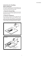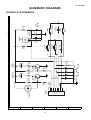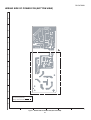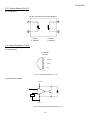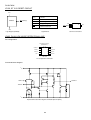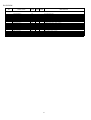
1
DV-SL700W
SERVICE MANUAL
No. S9501DVSL700W
DVD PLAYER
MODEL
DV-SL700W
• In the interests of user-safety (Required by safety regulations in some countries) the set should be restored to its
original condition and only parts identical to those specified
be used.
CONTENTS
Page
SAFETY PRECAUTION FOR SERVICE MANUAL ............................................................................................................... 2
AC POWER SUPPLY CORD................................................................................................................................................. 2
SPECIFICATIONS ................................................................................................................................................................. 3
LASER BEAM SAFETY PRECAUTIONS .............................................................................................................................. 4
STANDARD NOTES FOR SERVICING................................................................................................................................. 5
OPERATING CONTROLS AND FUNCTIONS ...................................................................................................................... 8
BLOCK DIAGRAMS.............................................................................................................................................................. 10
SCHEMATIC DIAGRAMS..................................................................................................................................................... 11
IC’S PIN VOLTAGE CHART ................................................................................................................................................ 22
WAVEFORMS....................................................................................................................................................................... 25
OVERALL WIRING CONNECTION...................................................................................................................................... 28
WIRING DIAGRAM............................................................................................................................................................... 29
NOTES ON SCHEMATIC DIAGRAM / TYPES OF TRANSISTOR AND LED ...................................................................... 39
TROUBLESHOOTING.......................................................................................................................................................... 40
IC PIN FUNCTION DESCRIPTIONS.................................................................................................................................... 41
PARTS GUIDE/EXPLODED VIEW
Parts marked with " " are important for maintaining the safety of the set. Be sure to replace these
parts with specified ones for maintaining the safety and performance of the set.
1
This document has been published to be used for
after sales service only.
The contents are subject to change without notice.
DV-SL700W
SAFETY PRECAUTION FOR SERVICE MANUAL
l This product is classified as a CLASS 1 LASER PRODUCT.
l
WARNINGS:
The AEL (Accessible Emission Level) of Laser Power Output for this model is specified to be lower than Class 1
Requirements. However, the following precautions must be observed during servicing to protect your eyes against
exposure to the Laser beam.
(1) When the cabinet has been removed, the power is turned on without a compact disc, and the Pickup is on a
position outer than the lead-in position, the Laser will light for several seconds to detect a disc. Do not look into
the Pickup Lens.
(2) The Laser Power Output of the Pickup inside the unit and replacement service parts have already been adjusted
prior to shipping.
(3) No adjustment to the Laser Power should be attempted when replacing or servicing the Pickup.
(4) Under no circumstances look directly into the Pickup Lens at any time.
(5) CAUTION - Use of controls or adjustments, or performance of procedures other than those specified herein may
result in hazardous radiation exposure.
AC POWER SUPPLY CORD
92LVPE00327911
92LVPE41A25310
2
DV-SL700W
SPECIFICATIONS
As part of our policy of continuous improvement, SHARP reserves the right to make design and specification changes
for product improvement without prior notice. The performance specification figures indicated are nominal values of
production units. There may be some deviations from these values in individual units.
l General
Power source
Power consumption
Dimensions
Weight
Audio output terminals
Video output terminals
Digital output terminal
l DVD Player
Signal system
Supported disc types
Video signal
Audio signal
AC110 - 240 V, 50/60 Hz
Power on: 15 W
Width: 360 mm (14-3/8”)
Height: 37 mm (1-1/2”)
Depth: 200 mm (7-7/8”)
1.5 kg (3.3 lbs)
Analogue output (OUT): RCA type x 1 pair (L/R)
S-video output: S-terminal x 1, component (Y, PB,PR)
Video output: RCA type x 1
COAXIAL
PAL/NTSC colour
DVD (with the same region number on the back of the unit or ALL), SVCD, VCD, audio CD, CDR, CD-RW, MP3, JPEG
Horizontal resolution: 500 lines
S/N ratio: 70dB
Linear PCM DVD: 20 Hz to 20 kHz (sampling rate: 48 kHz)
Frequency characteristics
20 Hz to 20 kHz (sampling rate: 96 kHz)
CD: 20 Hz to 20 kHz
S/N ratio
CD: 94 dB (1 kHz)
Dynamic range
Linear PCM DVD: 95 dB
CD: 94 dB
Total harmonic distortion ratio 0.01% maximum
3
DV-SL700W
LASER BEAM SAFETY PRECAUTIONS
This DVD player uses a pickup that emits a laser beam.
Do not look directly at the laser beam coming
from the pickup or allow it to strike against
Do not look directly at the laser beam coming
your skin.
from the pickup or allow it to strike against
your skin.
The laser beam is emitted from the location shown in the figure. When checking the laser diode, be sure to keep your
eyes at least 30cm away from the pickup lens when the diode is turned on. Do not look directly at the laser beam.
The laser beam is emitted from the location shown in the figure. When checking the laser diode, be sure to keep your eyes at least
30cm away from the pickup lens when the diode is turned on. Do not look directly at the laser beam.
Caution: Use of controls and adjustments, or doing procedures other than those specified herein, may result in hazardous radiation
exposure.
Drive Mecha Assembly
Drive Mecha Assembly
Laser Beam Radiation
Laser Beam Radiation
Laser Pickup
Laser Pickup
Turntable
Turntable
4
DV-SL700W
STANDARD NOTES FOR SERVICING
(1)
Using desoldering
remove
the solder from all
Using
lead-freebraid,
wire
solder
pins of the flat pack-IC. When you use solder flux
When
fixing
the PWB
soldered
thepack-IC,
lead-freeyou
solder,
which
is applied
to all
pins of with
the flat
can
apply
lead-free
wire
solder.
Repairing
with
conventional
remove it easily. (Fig. S-1-3)
lead wire solder may cause damage or accident due to
cracks.
Flat Pack-IC
Desoldering Braid
As the melting point of lead-free solder (Sn-Ag-Cu) is
higher than the lead wire solder by 40°C, we recommend
you to use a dedicated soldering bit, if you are not
familiar with how to obtain lead-free wire solder or
soldening bit, contact our service station or service
ranch in your area.
Circuit
Board Indications
1.
Removal
a. The
outputFlat
pin of
the 3 pin
Regulator ICs
is indicated
With
Hot-Air
Pack-IC
Desoldering
Machine:
as shown.
(1) Prepare the hot-air flat pack-IC desoldering machine, then apply hot air to the Flat Pack-IC (about 5
to 6 seconds).
(Fig. S-1-1)
Top View
Bottom View
Out
In
Input
b. For other ICs, pin 1 and every fifth pin are indicated
as shown.
Soldering
< Bottom View >
Soldering Iron
As the melting point of lead-free solder (Sn-Ag-Cu)
Fig. S-1-3 is
about 220°C which is higher than the conventional lead
solder by 40°C, and as it has poor solder wettabillty, you
(2) Lift each lead of the flat pack-IC upward one by one,
may be apt to keep the soldering bit in contact with the
using a sharp pin or wire to which solder will not
PWB for extended period of time. However, Since the
adhere (iron wire). When heating the pins, use a fine
land may be peeled off or the maximum heat-resistance
tip soldering iron or a hot air desoldering machine.
temperature of parts may be excoeded, remove the bit
(Fig. S-1-4)
from the PWB as soon as you conurm the steady
soldering condition.
Lead-free solder contains more tin, and the end of the
soldering bit may be easily corroded. Make sure to tum
on and off the power of the bit as required. if a different
type of solder stays on the tip of the soldering bit, it is
alloyed with lead-free solder. Clean the bit after every
use of it.
Sharp
Pin during
When the tip of the soldering bit is blackened
use, file it with steel wool or fine sandpaper.
Becareful
when
Fine
Tipreplacing parts with polarity indication
on the PWB
silk. Iron
Soldering
Fig. S-1-4
5
Pin 1
Fig. S-1-1
10
(2) Remove the flat pack-IC with tweezers while applyc. ing
Thethe
1sthot
pinair.
of every male connector is indicated as
shown.
(3) Bottom of the flat pack-IC is fixed with glue to the
CBA; when removing entire flat pack-IC, first apply
< Bottom View
> center of the flat pack-IC and heat
soldering
iron to
up. Then remove (glue will be melted). (Fig. S-1-6)
Pin 1the flat pack-IC from the CBA using twee(4) Release
zers. (Fig. S-1-6)
Caution:
Instructions
for
Connectors
1.
Do not supply hot
air to
the chip parts around the flat
pack-IC for over 6 seconds because damage to the
1. When you connect or disconnect the FFC (Flexible
chip parts may occur. Put masking tape around the
Foil Connector) cable, be sure to first disconnect the
flat pack-IC to protect other parts from damage.
AC cord.
(Fig. S-1-2)
2. FFC (Flexible Foil Connector) cable should be in2. The flat pack-IC on the CBA is affixed with glue, so
serted parallel into the connector, not at an angle.
be careful not to break or damage the foil of each pin
or the solder lands under the IC when removing it.
FFC Cable
Lead-free
solder
for servicing
(3)
Bottom wire
of the
flat pack-IC
is fixed with glue to the
CBA; when removing entire flat pack-IC, first apply
Part No.
Description
Code
soldering iron to center of the flat pack-IC and heat
0.3mm
250g(1roll)
BL
ZHNDAi123250E
J
up. Then remove (glue
will
be melted).
(Fig. S-1-6)
(4)
Release the flat pack-IC
from
the500g(1roll)
CBA using tweeZHNDAi126500E
J
0.6mm
BK
zers. (Fig. S-1-6)
1.0mm 1kg(1roll)
BM
ZHNDAi12801KE J
Hot-air
Flat Pack-IC
Desoldering
Machine
With Iron Wire:
CBA
(1) Using desoldering braid, remove the solder from all
pins of the flat pack-IC. When you use solder flux
which is applied to all pins of the flat pack-IC, you can
remove it easily. (Fig. S-1-3)
Connector
CBA
Masking
Tape
* Be careful
Tweezers
(2) Affix the wire to a workbench or solid mounting point,
as shown in Fig. S-1-5.
Flat Pack-IC
(3) While heating the pins using a fine tip soldering iron
or hot air blower, pull up the wire as the solder melts
so as to lift the IC leads from the CBA contact pads
as shown in Fig. S-1-5.
to avoid a short circuit.
Fig. S-1-2
5
DV-SL700W
How
to Remove / Install Flat Pack-IC
(4) Bottom of the flat pack-IC is fixed with glue to the
With Soldering Iron:
2. Installation
(1) Using desoldering braid, remove the solder from all
(1) pins
Usingofdesoldering
braid, remove
the use
solder
from flux
the
the flat pack-IC.
When you
solder
foil of each
pin oftothe
onpack-IC,
the CBAyou
so you
which
is applied
all flat
pinspack-IC
of the flat
can
can install
a replacement
flat pack-IC more easily.
remove
it easily.
(Fig. S-1-3)
CBA; when removing entire flat pack-IC, first apply
1. Removal
soldering iron to center of the flat pack-IC and heat
up.Hot-Air
Then remove
(glue will
be melted).Machine:
(Fig. S-1-6)
With
Flat Pack-IC
Desoldering
(5) Prepare
Release the
pack-IC
from the desoldering
CBA using twee(1)
the flat
hot-air
flat pack-IC
mazers. (Fig.
chine,
thenS-1-6)
apply hot air to the Flat Pack-IC (about 5
to 6 seconds). (Fig. S-1-1)
Note:
(2) The "●" mark on the flat pack-IC indicates pin 1. (See
Fig.
matches Braid
the 1 on the
Flat S-1-7.)
Pack-ICBe sure this mark
Desoldering
PCB when positioning for installation. Then presolder the four corners of the flat pack-IC. (See Fig. S1-8.)
When using a soldering iron, care must be taken to
ensure that the flat pack-IC is not being held by glue.
When the flat pack-IC is removed from the CBA,
handle it gently because it may be damaged if force
is applied.
(3) Solder all pins of the flat pack-IC. Be sure that none
of the pins have solder bridges.
Example :
Soldering Iron
Hot Air Blower
Fig. S-1-3
(2) Lift each lead of the flat pack-IC upward one by one,
using a sharp pin or wire to which solder will not
adhere (iron wire). When heating the pins, use a fine
tip soldering iron or a hot air desoldering machine.
(Fig. S-1-4)
or
Fig. S-1-1
Ironwhile
Wire apply(2) Remove the flat pack-IC with tweezers
ing the hot air.
Pin 1 of the Flat Pack-IC
is indicated by a " " mark.
(3) Bottom of the flat pack-IC is fixed
with glue
Soldering
Ironto the
CBA; when removing entire flat pack-IC, first apply
soldering
To Solidiron to center of the flat pack-IC and heat
up.
Then remove
Mounting
Point (glue will be melted). (Fig. S-1-6)
(4) Release the flat pack-IC from the CBA Fig.
usingS-1-5
tweezers. (Fig. S-1-6)
Presolder
Sharp
Pin
Caution:
1. Do not supply hot air to the chip parts around
Fine Tipthe flat
CBA for over 6 seconds because damage
pack-IC
the
SoldeingtoIron
chip parts may occur. Put masking tape around the
flat pack-IC to protect other parts from damage.
(Fig. S-1-2)
Fine Tip
Soldering Iron
Fig. S-1-4
(3) Bottom of the flat pack-IC is fixed with glue to the
Flat Pack-IC
CBA; when removing entire flat pack-IC,
first apply
soldering iron to center of the flat pack-IC and heat
CBA
up.
Then remove (glue will be melted). (Fig. S-1-6)
Fig. S-1-8
(4) Release the flat pack-IC from the CBA using tweezers. (Fig. S-1-6)
2. The flat pack-IC on the CBA is affixed with glue, so
be careful not to break or damage the foil of each pin
or the solder lands under the IC when removing it.
Flat Pack-IC
Tweezers
Fig. S-1-7
Hot-air
Flat Pack-IC
Fig. S-1-6
Desoldering
Machine
With Iron Wire:
CBA
(1) Using desoldering braid, remove the solder from all
pins of the flat pack-IC. When you use solder flux
which is applied to all pins of the flat pack-IC, you can
6
DV-SL700W
(4) Bottom of the flat pack-IC is fixed with glue to the
Instructions
for Handling
CBA; when removing
entire flat pack-IC, first apply
soldering iron to center of the flat pack-IC and heat
Semi-conductors
up. Then remove (glue will be melted). (Fig. S-1-6)
Electrostatic breakdown of the semi-conductors may
(5)
Release
flat pack-IC
fromcaused
the CBA
tweeoccur
due to athe
potential
difference
by using
electrostatic
zers.
(Fig.
S-1-6)
charge during unpacking or repair work.
Note:
1. Ground
for
Human iron,
Body
When using
a soldering
care must be taken to
ensure
that
the
flat
pack-IC
is
not
being
held
by glue.
Be sure to wear a grounding band (1MΩ)
that
is properly
When
the
flat
pack-IC
is
removed
from
the
CBA,
grounded to remove any static electricity that may
be
handle
it
gently
because
it
may
be
damaged
if
force
charged on the body.
is applied.
2. Installation
(1) Using desoldering braid, remove the solder from the
foil of each pin of the flat pack-IC on the CBA so you
can install a replacement flat pack-IC more easily.
(2) The "●" mark on the flat pack-IC indicates pin 1. (See
Fig. S-1-7.) Be sure this mark matches the 1 on the
PCB when positioning for installation. Then presolder the four corners of the flat pack-IC. (See Fig. S1-8.)
(3) Solder all pins of the flat pack-IC. Be sure that none
of the pins have solder bridges.
2. Ground for Workbench
Example :
Be sure to place a conductive sheet or copper plate with
Hot Air Blower
proper grounding (1MΩ) on the workbench or other
surface, where the semi-conductors are to be placed.
Because the static electricity charge on clothing will not
escape through the body grounding band, be careful
or to
avoid contacting semi-conductors with your clothing.
Iron Wire
< Incorrect >
Pin 1 of the Flat Pack-IC
is indicated by a " " mark.
Soldering Iron
To Solid
Mounting Point
Fig. S-1-7
Presolder
Fig. S-1-5
CBA
Fine Tip
Soldeing Iron
CBA
Flat Pack-IC
< Correct >
Grounding Band
CBA
Fig. S-1-8
Flat Pack-IC
Tweezers
Fig. S-1-6
CBA
Conductive Sheet or
Copper Plate
7
DV-SL700W
OPERATING CONTROLS AND FUNCTIONS
n Main unit (front panel)
1
2 3
4 5 6 7
8
1.
Disc Tray
5.
Disc Tray OPEN/CLOSE Button
2.
STANDBY Indicator
6.
Play or Pause Button
3.
PLAY/PAUSE Indicator
7.
STOP Button
4.
Remote Sensor
8.
ON/STANDBY
n Main unit (rear panel)
1
2
3
4 5 6
1. AC Cord Lead
4. Digital Output Socket(Coaxial)
2. Component Video Output Sockets
5. Audio Output Sockets
3. Video Output Socket
6. S-Video Output Socket
8
DV-SL700W
n Remote control
1.
Remote Control Transmitter
2.
MENU/PBC Button
3.
Disc Tray Open/ Close Button
4.
Title Select Button
5.
Fast Backward/Chapter (track) skip down
11
6.
Fast Forward/Chapter (track) skip up
5
12
13
7.
Direct Number Buttons
6
14
8.
PROGRAM / ANGLE Button
9.
MUTE Button
1
2
3
4
10
15
7
8
9
10. ON/STANDBY Button
16
11. SETUP/GO TO Button
17
18
12. SLOW Button
19
13. STOP Button
20
21
14. ENTER / PLAY / PAUSE Button
15. Cursor Up and Down Buttons
16. Subtitle Select Button
17. Audio Select Button
18. Repeat A - B Button
19. Repeat Play Button
20. ZOOM Button
21. DISPLAY Button
9
AC~110-240V
POWER
LOADER
M07S
STANDBY
P+5V
GND
P+12V
SUNPLUS
SHPE8202D
Figure 1: BLOCK DIAGRAM
10
8550SS
+1.8V
8550SS
+3.3V
MOTOR
AM5869
RESET
CM3403-29SO
SDRAM
512X16X2
IR
KEY
LED
EEPROM
AF24BC02
FLASH
MX29LV040T
C-70
SPDIF OUT
Y.U.V
VIDEO OUT
S-VIDEO OUT
O/P
4558
L-OUT
R-OUT
AUDIO OUT
COAXIAL
Pr
Pb
Y
SVIDEO OUT
VIDEO OUT
R-OUT
L-OUT
DV-SL700W
BLOCK DIAGRAMS
1
G
2
62PIN
63PIN
3
11
4
Figure 1: CONTROL PCB SCHEMATIC
GND
LED2
LED3
5
R204
1K
Q302
2SA733
R208
4.7K
R207
10K
R202
560
D102 D103 D104 D105
1N4148
1N4148
1N4148
1N4148
IR
VCC
CS
DATA
CLK
Q301
2SA733
R201
560
C12
104
1N4148
D203
ON/STD BY
TA202
EJECT
TA201
C
8
7
6
5
4
3
2
1
R203
1K
F
R209
4.7K
R205
10K
TA203
D101
1N4148
R206
10
STOP
TA204
D204
1N4148
PLAY/PAUSE
+
C14
100uF/16V
SN201
IRT
B
RB201
IR/VFD
+
D202
RED LED
E
C13
330uF/10V
D201
GREEN LED
DV-SL700W
SCHEMATIC DIAGRAMS
CONTROL PCB SCHEMATIC
A
D
H
6
DV-SL700W
MAIN PCB SCHEMATIC
A
B
Pickup head parameter
Sony
Motor Driver AM5668
Motor Driver AT5660
R40
R39
R14
R15
R53
R62
C32
R63
C33
4.7
4.7
100
100
20K
12K
1500P
68K
1000P
R62
3.3K
C32
R63
C33
2700P
39K
1000P
Sanyo
5.1
5.1
0
0
2.2K
33K
1000P
68K
1000P
20K
1000P
39K
1000P
Samsung
5.1
5.1
0
0
2.2K
12K
1500P
68K
1000P
3.3K
2700P
39K
1000P
Mitsumi
5.1
5.1
0
0
2.2K
12K
1500P
68K
1000P
3.3K
2700P
39K
1000P
C
DVCC33
VCC1.8
PL
C101
C102
C103
C104
C105
C106
C107
C108
0.1UF
0.1UF
0.1UF
0.1UF
0.1UF
0.1UF
0.1UF
0.1UF
G
GND
28
25
GND
D
RF+5V
TP3
RAD+
C
D
FOC+
TP2
RAD-
PUHRF
B
GND
VREF1
C177
0.1U
C179
0.1U
GND
R143
R144
PUH_CDLD#L11
CDVR
DVD_VR#
0
0
CD_VR
CD_VR
DVD_VR
DVD_VR
10UH PUH_CDLD
10UH PUH_DVDLD
0.1UF
GND
G
+
C119
0.1UF
+
LDSW
RF3.3V
R154
5.1
C176
Q101
100UF10V
PUH_CDLD
27
26
ELCO-CON24(Left)
BOTTOM CONTACT
RF+5V
RF+5V
100K
2SK3018
GND
0.1U
CN101
C118
Q104
GR156
L12
R159
470
GND
FORVH
WR FRQQHFWRU
RF3.3V
C180
47UF16V
R145
C120
0.1UF
2SB1132
R155
+
C181
47UF16V
2SB1132
R146
0
5.1
Q102
0
CDLDO
CDMDI
100K
2SK3018
DVDMDI
PUH_DVDLD#
R157
G
Q103
E
GND
R158
470
S
F
C178
F
Q105
3904
A
PUH_DVDLD
D101
1N4148
D102
1N4148
GND
GND
DVDLDO
FOCTP1
DD
E
TP4
FOCFOC+
RAD+
RAD-
S
1
2
3
4
5
6
7
8
9
10
11
12
13
14
15
16
17
18
19
20
21
22
23
24
DIP28-SSOPH
H
FCO
1
2
1
TRB1
2
REGO3
3
IC105
AM5869S
25K
VINFC
BIAS
10K
TRB1
3
RFGO3
-
Actuator
Driver(6 x)
+
4
-
Figure 2: MAIN PCB SCHEMATIC (1/8)
12
VOFC+
VOFC-
5
RFGO1
14
FOC+
13
FOC-
5
RFGO1
6
DV-SL700W
MAIN PCB SCHEMATIC
RF3.3V
C112
C113
C114
0.1UF
0.1UF
0.1UF
TV0
TV3
TV4
TV
CVB
Y
Cb
C
CVB
CVB
Y
CVB
(S-Video)
G
C
(S-Video)
R
B
GND
PLL3.3V
VVCC3
107
C108
C109
C110
1UF
0.1UF
0.1UF
0.1UF
GND
DAC_REF
C153
C111
+
10UF16V
VGND
0.1UF
GND
C163
GND
R109
C154
GND
680PF
C159
1UF
1.5K
0.01UF
C164
1UF
C185 NC(120PF)
1
2
3
4
TP11
5
C156 680PF
RFIP
6
DPDA
C157 680PF
7
8
DPDC
9
C158 680PF
10
D
11
C
12
B
13
A
14
CDB
CDB
TP8
15
CDA
CDA
TP9
16
F
F
TP7
17
E
E
TP6
18
GND
19
20
DVDLDO
21
CDLDO
C182
47UF16V
22
DVDMDI
23
CDMDI
24
RF3.3V
C122
0.1UF
25
VREF1
GND
R163
33K (1%)26
GND
VREF2
27
C188 0.22UF 28
+
C121
C183
C161 0.01UF
29
GND
0.1UF
C162 0.01UF 30
47UF16V
31
RFCT
RFCT TP5
C186 0.047UF
32
C184 300PF
33
SBAD
C187 820PF
34
FEO
35
GND
R160
NG
TEO
36
C210 0.1U
GND
7
8
C213 330PF
37
XOPVIP1
GND
38
XOPVIN1
39
XOPOP1
TCO
40
GND
C155
16V
146
680PF
Vref0
PD
FD
5.1K
5.1K
C160
0.01UF
LGIN
R114
150K
100PF
20K
GND
PLL3.3V
PLL3.3V
VGND
GND
GND
GND
DVCC33
DVCC
216
215
214
213 RFRP
212 C123 0.1UF
1.2K (1%)
211 R164
210
209
208
207
206
205
204
203
202
201
200
199
198
197
196
195 R/V
194
193 B/U
192 G/Y
191
190
189
188
187 CVBS1
186 V_REF
185 V_FSADJ
184 V_BIAS
183 V_COMP
182 V_V_SYNC
181 V_H_SYNC
180 AU_XCK
179 AU_BCK
178
177 AU_LRCK
176 AUDIO_MUTE
175 AU_D2
174 AU_D1
173
172 AU_D0
171 SPDIF_OUT
170 RA18
169 RA16
168
167
166 DA R
RF3.3V
VVCC3
FLTIN
FLTIP
RFO
RFRP
AGCCAP
GMRES
RF_AVDD
DS_AVDD
SLVL
CNIN
RFI
PLL_DS_AVSS
LGIN
LPFNIN
FDFLT
PDFLT
VREFO
LPFN
LPFO
PLL_AVDD
VSS_TVA2
TV_DAC5
VDD_TVA2
TV_DAC4
TV_DAC3
VSS_TVA1
VDD_TVA1
VSS_TVA0
VDD_TVA0
TV_DAC0
V_REFOUT
V_FSADJ
V_BIAS
V_COMP
UA0_TX/GPIO
UA0_RX/GPIO
A_XCK/GPIO
A_BCK/GPIO
VSS_K6/VSS_O6
A_LRCK/GPIO
A_DATA3/GPIO
A_DATA2/GPIO
A_DATA1/GPIO
VDD_O5
A_DATA0/GPIO
A_IEC_TX/GPIO
R_A18
R_A16
DAC_VSS
DAC_VDD
DA R
RFIP
PUHRF
47PF
R112
R113
C168
RFO
1UF
1UF
C170
C167 0.068UF
TP24
RFRP
C165
C166
47PF
RFI
R110
GND
C169
+
AGCON
AGCOP
RFIP
RFIS
RFSUM
DPDA
DPDB
DPDC
DPDD
DVDD
DVDC
DVDB
DVDA
CDB
CDA
CDF
CDE
RF_AVSS
APC_AVSS
DVDLDO
CDLDO
DVDMDI
CDMDI
APC_SRV_AVDD
V21
R33K
V165
SVOTST
RFRPPH
RFRPBH
RFRPMEAN
SBADPH
SBAD
FEO
TEO
TEOLP
9
OPVIP
OPVIN
OPVOP
SRV AD AVSS VRGD
IC101
SPHE8202S(D)-216PIN
10
Figure 2: MAIN PCB SCHEMATIC (2/8)
13
11
12
DV-SL700W
MAIN PCB SCHEMATIC
A
R
SPDIF_OUT
10
TV3
B
TV4
TV5
Cb
Cr
Y
Y
C
CVB
deo)
B
G
ZD301
(S-Video)
R
6.8V
VCC
ZD304
6.8V
VCC VGND
VVCC3
C
VGND
C171
NCV_BIAS
C115
0.1UF
R302
75 OHM
ZD306
VGND
6.8V
VCC
R303
ZD307
6.8V
75 OHM
ZD303
6.8V
VGND
V_COMP
0.1UF
V_REF
0.1UF
V_FSADJ
390
C117
VGND
R137
VGND
ZD302
6.8V
AU_BCK
⿌㝍
AU_LRCK
Ȳǵⵦ㝍
AU_XCK
⠻㝍
C173
GND
H
1
SDIN
AOUTR
DEM/SCLK
VA
LRCK
AGND
MCLK
AOUTL
VQ
FILT+
CS4344(NC)
C191
104
IC401B
XCK
LRCK
DIN
BCK
TST
VCM
GND
13
12
FMT
DEM
L-OUT
R1
VGND
75 OHM
R301
R304
75 OH
V
ZD308
6.8V
VGND
R401 12K
VCC
R140
33
L1
C174
C194
C196
C195
10UF
104
100UF
104
R428
R430 3K
10UF
1.5K
C422 C425
562 562
2
2.4K
3
104
C412
C409
181
4.7K
C403
R429
R431 3K
10UF
1.5K
C423 C424
562 562
8
VCC
C408
180
R403
R402 12K
R134
9
6
AL
AR
C401
6
R404 2.4K
5
CF2752(NC)
10
C413
RB101
8
7
6
5
R405 10K R406 10
RA12
1
2
3
4
C416
RA7
RA6
RB102
8
7
6
5
33
RA0
RA5
100UF
RA4
1
2
3
4
C414
RA3
RA2
RA1
104
33
RD0
RD1
vcc
RD2
RD3
R416
2K
RD4
RD5
R421
1K
RD6
RB105
8
VCC1.8 7
PIN_142
PIN_141
6
5
RD7
1
2
3
4
ROE
DQM2
DQM3
RB106
8
7
6
5
33
RB107 DVCC33
MA3
vcc
GND
8
7
6
5
R418
1K
+12V
vcc
R423
162
161
160
159
158
157
156
155
154
153
152
151
150
149
148
147
146
145
144
143
142
141
140
139
138
137
136
135
134
133
132
131
130
129
128
127
126
125
124
123
122
R419
10K
G
R_A12
R_A7
R_A6
R_A5
R_A4
R_A3
R_A2
R_A1
R_A0
R_D0
R_D1
R_D2
VSS_O5/VSS_K5
R_D3
R_D4
R_D5
R_D6
R_D7
R_OE_B
VDD_K4
M_DQM2/GPIO
M_DQM3/GPIO
R_A10
R_A11
R_A9
R_A8
VDD_O4
R_A13
R_A14
R_A17
R_WE_B
M_A3
M_A2
M_A1
VSS_O4/VSS_K4
M_A0
2M_A10
M_BA1/GPIO
M_DQM0/GPIO
M DQM1/GPIO
10
9
8
7
6
1
2
3
4
1
2
3
4
R417
1K
RA10
Q403
2N3906
1K
Q404
2N3906
220UF/16V
vcc
D404
R432
1N4001
6.8K
Q405
2N3906
R420
1K
C427
220UF
POWER NO
R43
47k
C421
RA11
RA9
RA8
33
RA13
RA14
AUDIO_MUTE
_
V_COMP
UA0_TX/GPIO
UA0_RX/GPIO
A_XCK/GPIO
A_BCK/GPIO
VSS_K6/VSS_O6
A_LRCK/GPIO
A_DATA3/GPIO
A_DATA2/GPIO
A_DATA1/GPIO
VDD_O5
A_DATA0/GPIO
A_IEC_TX/GPIO
R_A18
R_A16
DAC_VSS
DAC_VDD
DA_R
DA_L
DAC_REF
R_A15
F
R139
R136
IC401
14
1
2
3
4
5
7
RA15
DA_R
DAC_REF
DA_L
RA16
DVCC33
RA18
SPDIF_OUT
AU_D0
AU_D1
AU_D2
AUDIO_MUTE
AU_BCK
AU_XCK
V_H_SYNC
V_V_SYNC
DVCC33
10UF
183
182
181
180
179
178
177
176
175
174
173
172
171
170
169
168
167
166
165
164
163
AU_LRCK
GND
E
V_COMP
NC R-OUT
NC(0)
NC(0)
NC
R135
R138
1
2
3
4
5
V
6.8V
D
ៜ㝍
VGND
VCC
VGND
1/2 current config
AU_D0
VGND
ZD305
C116
VVCC3
V
LMUTE
AUDIO MUTE
RA17
RWE
33
MA2
MA1
MA0
MA10
GND
3
4
5
6
PIN_125
DQM0
DQM1
RA16
Figure 2: MAIN PCB SCHEMATIC (3/8)
14
1
2
A16
DV-SL700W
MAIN PCB SCHEMATIC
VCC
VGND
R303
VGND
VGND
M
R304
75 OHM
VGND
VGND
L302
2.4UH
C303
470PF
VGND
C307
470PF
VGND
C304
L304
470PF
2.4UH
VGND
10UF
2
Q407
2N3906
470
Q401
2N3904
101
2
8
C416
8
4
RCA4
5
C312
101
C311
C313
101
101
7
6
2
+12V
10OHM
C426 R434
100UF 104
2
C410
101
C411
101
RO
R413 1k
R414 NC
+12V
R310
1K
00UF
601
1
R439
3K
SC-R IN
R-OUT
R411 1k
IC402B
NJM4558
C404
8
B IN
1
LMUTE
R412 1k
C405
10UF
10K R406 10K
3
FB402 601
R437
C409
181
104
2
VGND
FB401
413
R IN
C310
101
470
7
1
2
C308
470PF
R438
5
2
Q402
2N3904
IC402A
NJM4558
6
JK101
FB309 101
1
G IN
R408 1k
1
4
FB307
1
RCA+SVIDEO
2
R407 1k
R409 NC
R410 1k
SC-L IN
L-OUT
LO
K
4K
B/U_O
VGND
FB308 101
1
2
101
FB303
1
VGND
2.4UH
YY
CC
9
101
FB302
1
C402
3
2
R/V_O
C306
470PF
L303
C408
180
104
412
101
FB301
1
G/Y_O
K
4K
SC-L IN
VGND
C302
470PF
75 OHM
VGND
C305
470PF
C301
470PF
75 OHM
VGND
15PF
2.4UH
L301
R302
C309
15PF
7
R308
1K
100
JK102
2
1
4
3
5
6
C316
SPDIF_OUT
101
2
CVBS IN
101
2
101
2
C314
R305
FB304
FB305
FB306
CVB1_O-1 1
1
G/Y_O
1
R/V_O
R306
100
15PF
10K
C315
R309
200
15PF
Q305
C945
R307
SC8
VCC
414
ZD309
6.8V
104
vcc
SC1
R311
4.7K
R420
1K
R312
Q308
2N3904
4.7K
Q307
2N3904
L-OUT
SC2
27
UF
R433
47k
SC16
R313
75
+12V
R-OUT
Q406
2N3906
FB403 NC
FB404 NC
1
1
1
CN401
2
2
1
2
3
4
2
FB405
NC
C431
NC
POWER OFF
C430
NC
C432
NC NC
SC-R IN 1
SC-L IN
7
1
8
40
9
1
IC103A
10
32
B IN
Figure 2: MAIN PCB SCHEMATIC (4/8)
15
3
5
7
JK103
R IN
L IN
AGND
GND
2
4
6
11
12
DV-SL700W
GND
FORVH
WR FRQQHFWRU
A
D101
1N4148
D102
1N4148
GND
GND
DVDLDO
MAIN PCB SCHEMATIC
DIP28-SSOPH
1
FCO
TRB1
2
REGO3
3
25K
IC105
AM5869S
10K
VINFC
BIAS
+
C125
GND
26
VREF2
27
0.1UF TRB3 25
24
-
RFGO3
SPDCO
C
4
14
FOC+
13
FOC-
-
VOTK+
Actuator
Driver(6 x)
+
BIAS
VOTK-
15
RAD+
16
RAD-
TRB3
TRB2
20
REGO2
+
10K
VINSP
-
R149
VOSP-
Actuator
Driver(4 x)
11
VOSP+
23
+
10K
VINSL
VOSL+
Actuator
-
Driver(4 x)
VOSL-
6
TRAY-
7
8
19
M+5V
C124 C126
FWD
C198
100UF16V
22
0.1UF 0.1UF
GND
CN102
E
FB124
FB125
C209
C207
1
R115
DMEA
9
LOAD-
LOAD+
XT1
27MH
AT5660
R171
4.7K
C199
33PF
SLED+
SP-
601
601
601
FB129
GND
SP+
LOADLOAD+
601
TRAYOUT
R173
4.7K
TRAYIN
R174
4.7K
VCC
33PF
33PF
33PF
S-BY
601
601/2AVCC
FB902
FB903
FB904
FB905
601
601
601
601
VCC
+12V
-27V
AC1
AC2
C936
C925 C901 C921
100UF16V
104
FB910
FB
0.1UF 104
GND
2
3
4
Figure 2: MAIN PCB SCHEMATIC (5/8)
16
5
RF+5V
C905
0.1UF
GND
H
1
R905
2.2
M+5V
C904
0.1UF
104
POWER
FB907
FB901
C934
100UF16V
C923
G
SANDBY
P+5V
GND
P+12V
P-27V
PAC1
PAC2
104 C929
104 C930
104 C931
104 C932
7
6
5
4
3
2
1
104 C926
104 C927
CN901
33PF
33PF
C202
33PF
C204
33PF
C206
33PF
C208
33PF
C205
SLED-
HOME
GND
C201
18
SLED-
601
601
FB126
FB127
FB128
C203
CN103
601
601
601
GND
JST-CON6-2 mm
F
NC
GND
FB120
FB121
FB123
1
2
3
4
5
6
5
4
3
2
1
SLED+
10
VOLD+
Vcc1
Vcc2
0
150K
VOLD-
TRAY DRIVER
Pre-DRV
REV
GND2
TRAY+
GND1
D
SP+SNSR
30
0
NC
SP+
17
28
STBY
VCTL
PreGND
21
29
R148
GND
R170
15K
M+5V
C127
0
SP-
R167
R150
25K
BIAS
R166
GND
12
0
SCO
RFGO1
25K
10K
VINTK
5
RFGO1
+
BIAS
R147
VOFC-
TRB1
B
TCO
VOFC+
Actuator
Driver(6 x)
6
DV-SL700W
MAIN PCB SCHEMATIC
16
17
18
GND
19
20
DVDLDO
21
CDLDO
C182
47UF16V
22
DVDMDI
23
CDMDI
24
RF3.3V
25
C122
0.1UF
VREF1
GND
R163
33K (1%)26
GND
VREF2
27
C188 0.22UF 28
+
C121
C183
C161 0.01UF
29
GND
0.1UF
C162 0.01UF 30
47UF16V
31
RFCT
RFCT TP5
C186 0.047UF
32
33
C184 300PF
SBAD
C187 820PF
34
FEO
35
GND
R160
NG
TEO
36
C210 0.1U
GND
C213 330PF
37
XOPVIP1
GND
38
XOPVIN1
39
XOPOP1
40
TCO
GND
41
C211 1000PF
GND
RF3.3V
R175
68K 42
C212 1000PF FCO R111
33K 43
44
GND
45
TRAYIN
46
TRAYOUT
C127 0.1UF
R176
2.2K 47
SPDCO
C128 0.1UF
R177
2.2K 48
SCO
49
TRAY50
TRAY+
51
DMEA
52
FGIN
FGIN TP10
53
HOME
R172
4.7K
54
LDSW
VCC
TP7
TP6
CDF
CDE
RF_AVSS
APC_AVSS
DVDLDO
CDLDO
DVDMDI
CDMDI
APC_SRV_AVDD
V21
R33K
V165
SVOTST
RFRPPH
RFRPBH
RFRPMEAN
SBADPH
SBAD
FEO
TEO
TEOLP
OPVIP
OPVIN
OPVOP
SRV_AD_AVSS_VRGD
AD_DA_AVDD
DATEO
DAFEO
DA_AVSS
TRAY_IS_IN
TRAY_IS_OUT
SPDC_OUT/GPIO
SC_OUT/GPIO
SC1_OUT/GPIO
TRAY_OUT/GPIO
DMEA/GPIO
FGIN/GPIO
HOMESW/GPIO
LDSW/GPIO
F
E
C215
4700PF
VCC1.8
DVCC33
R171
IC120
LM809
C216
104
4.7K
C199
33PF
GND
RF3.3V
C129
100K
R178
1
2
3
4
103
C219
GND
0.1UF
A0
A1
A2
GND
R905
2.2
GND
RF+5V
FB912
FB
12K
VCC1.8
R908
0.1UF
FB
RF3.3V
+
+
C913
0.1UF
0.1UF
VPLLVCC1.8
C938
FB918
FB
VVCC3
C908
220UF16V
0.1UF
10
C907
+
100uF
C920
104
GND
8
+
C919
100UF16V
VGND
9
10
Figure 2: MAIN PCB SCHEMATIC (6/8)
17
11
12
VCC1.8
MD10
MD11
MD12
MD13
MD14
MD15
M_CS0
GND
100UF16V
M_BA0
M_CAS
M_RAS
MWE
MD0
MD1
MD2
MD3
MD4
MD5
MD6
MD7
USB_DP
USB_DM
CLKOUT
CLKIN
VFD_DATA
RA19
C912
GND
7
CARD_WP
IR_IN
PLL3.3V
R9062.2
0.1UF
GND
VFD_STB
RESET_B
SD_VCC3
C916
C940
20K
RFGO1
0.1uF
R902
FB913
C942
R901
C941
C905
Q902
2SS8550D(1.5A;1W)
DVCC33
100uF
C939
0.1uF
10K
VFD_CLK
1.2R/0.5W
Q901
TRB1
2SCS8550D(1.5A;1W)
R903
R_CS1
R909
3.3R/0.5W
4.7K
REGO3
R142
1K
VCC
R907
VCC
R103 C130
33
0.1UF
DVCC33 GND
I2C ADDR = 0XA0
1N5401
R904
I2C_DATA
8
7
6
5
VCC
WP
SCL
SDA
24C01/CAT24C021 R141
1K
GND
D902
TRB3
I2C_CLK
GND
IC104
GND
APLLVCC3
DVCC33
601
VCC
C217
104
DVCC33
GND GND
VPLLVCC1.8
0.1UF
FB137
RESET_B
C200
33PF
VCC
GND
C911
USB_DP
USB_DM
T30
Reset
XT1
CLKIN
SC2
SC1
4700PF
CLKOUT
27MHz
CARD_SENSE2
470K
C214
LED3
150K
R151
0
XOPOP1
LED2
R162
S-BY
XOPVIP1
150K
XOPVIN1
V
P1
R116
1
R115
V
DFCT
R170
MS_BS
R161
470K
SPHE8202S(D)-216PIN
55
56
57
58
59
60
61
62
63
64
65
66
67
68
69
70
71
72
73
74
75
76
77
78
79
80
81
82
83
84
85
86
87
88
89
90
91
92
93
94
95
96
97
98
99
100
101
102
103
104
105
106
107
108
VREF2
P+
IC101
DFCT/GPIO
VDD_K1
GPIO/SD_CK/MS_CK
GPIO/SD_CMD/MS_BS
GPIO/ttio0_4/SD_D0/MS_D0
VSS_O1/VSS_K1
GPIO/ttio1_5/SD_D1/MS_D1
GPIO/ttio2_6/SD_D2/MS_D2
GPIO/ttio3_7/SD_D3/MS_D3
VDD_O1
GPIO
R_CS4_B/GPIO
R_CS3_B/GPIO
R_CS2_B/GPIO
R_CS1_B/GPIO
RST_B
IR_IN/GPIO
VFD_CLK/GPIO
VFD_STB/GPIO
VFD_DATA/GPIO
R_20/E_MX10
R_A19
CLKIN
CLKOUT
USB_GND
USB_VDD
USB_DP
USB_DM
VSS_PLLA
VDD_PLLA
VSS_PLLV
VDD_PLLV
M_D7
M_D6
M_D5
M_D4
M_D3
VDD_O2
M_D2
M_D1
M_D0
M_WE_B
M_CAS_B
M_RAS_B
VSS_O2/VSS_K2
M_CS0_B/GPIO
M_BA0
M_D15
M_D14
M_D13
VDD_K2
M_D12
M_D11
M D10
+
D
MS_CLK
F
E
DV-SL700W
MAIN PCB SCHEMATIC
A
_
M_D5
M_D4
M_D3
VDD_O2
M_D2
M_D1
M_D0
M_WE_B
M_CAS_B
M_RAS_B
VSS_O2/VSS_K2
M_CS0_B/GPIO
M_BA0
M_D15
M_D14
M_D13
VDD_K2
M_D12
M_D11
M_D10
B
RD6
RB105
8
VCC1.8 7
PIN_142
6
1
2
3
5
4
PIN_141
RD7
ROE
DQM2
DQM3
RB107
MA3
8
7
6
5
1
2
3
4
DVCC33
1
2
3
4
R417
1K
RB106
8
7
6
5
33
R419
10K
146
145
144
143
142
141
140
139
138
137
136
135
134
133
132
131
130
129
128
127
126
125
124
123
122
121
120
119
118
117
116
115
114
113
112
111
110
109
RA10
Q403
2N3906
1K
Q405
2N3906
1K
Q404
2N3906
C427
220UF
POWER NO
220UF/16V
R43
47k
C421
RA11
RA9
AUDIO_MUTE
R_D6
R_D7
R_OE_B
VDD_K4
M_DQM2/GPIO
M_DQM3/GPIO
R_A10
R_A11
R_A9
R_A8
VDD_O4
R_A13
R_A14
R_A17
R_WE_B
M_A3
M_A2
M_A1
VSS_O4/VSS_K4
M_A0
M_A10
M_BA1/GPIO
M_DQM0/GPIO
M_DQM1/GPIO
M_A4
VDD_K3
M_A5
M_A6
M_A7
M_A8
M_A9
M_CKE/GPIO
VSS_O3/VVV_K3
M_CLKO
VDD_O3
M_A11/GPIO
M_D8
M_D9
RA8
33
RA13
LMUTE
AUDIO MUTE
RA14
RA17
RWE
33
MA2
MA1
GND
MA0
MA10
PIN_125
DQM0
DQM1
RA16
MA4
RA15
VCC1.8
MA5
1
2
3
4
5
6
7
8
9
10
11
12
13
14
15
16
17
18
19
20
RA14
RA13
MA6
RA12
MA7
RA11
MA8
RA9
MA9
RA8
CKE
RWE
GND
SDRAM_CLK
SDRAM_CLK
DVCC33
MA11
RA18
MD8
RA7
MD9
RA6
RA5
C
RA4
RA3
RA2
RA1
A16
A15
A14
A13
A12
A11
A9
A8
WE#
NC
NC
NC
A18
A7
A6
A5
A4
A3
A2
A1
89
90
91
92
93
94
95
96
97
98
99
100
101
102
103
104
105
106
107
108
IC103C
R1
MD10
MD11
MD12
MD13
MD14
MD15
M_CS0
M_BA0
M_CAS
M_RAS
MWE
MD0
MD1
MD2
MD3
MD4
MD5
SD_VCC3
IC106
RB110
D
DVCC33
GND
1
2
3
4
MA0
VCC1.8
MA1
MA2
8
MA3
APLLVCC3
MA4
A0
A1
8
7
6
5
MA6
MA7
UF
MA8
MA9
MA10
M_BA0
SDRAM_CLK
E
33
33
33
33
R184
R185
R186
R187
C220
GND
10PF
A5
A6
A7
A8
A9
A10
BA0
RAM_CLK
CKE
RB113
8
7
6
5
M_RAS
M_CAS
MWE
1
2
3
4
R107
DQM1 R108
DQM0
F
A4
33
M_CS0
SD_VCC3
A3
1
2
3
4
33
R105
A2
RB111
33
MA5
30
8
7
6
5
CS0
RAS
CAS
S-MWE
21
22
23
24
27
28
29
30
31
32
20
19
35
34
18
17
16
15
33 14
33M-DQM0
33M-DQM1 36
33
37
C132
C133
C134
0.1UF
0.1UF
0.1UF
26
50
A0
A1
A2
A3
A4
A5
A6
A7
A8
A9
A10
BA/A11
CLK
CKE
CS
RAS
CAS
WE
DQ0
DQ1
DQ2
DQ3
DQ4
DQ5
DQ6
DQ7
DQ8
DQ9
DQ10
DQ11
DQ12
DQ13
DQ14
DQ15
VCC
VCC
DQML
DQMH
NC
NC
VCCQ
VCCQ
VCCQ
VCCQ
VSSQ
VSSQ
VSSQ
VSSQ
VSS
VSS
SDRAM 16M-6(512Kx16x2)
GND
RB114
2
D0
3
D1
5
D2
6
D3
8
D4
9 33 D5
11
D6
12
D7
39
D8
40
D9
42
D10
43
D11
45
D12
46 33 D13
48
D14
49
D15
1
2
3
4
MD0
8
7
6
5
MD1
1
2
3
4
RB116
1
2
3
4
1
25
8
7
6
5
SD_VCC3
7
13
38
44
MD2
RB115
MD3
MD4
8
7
6
5
MD5
MD6
MD7
MD8
33
MD9
MD10
RB117
1
2
3
4
33
MD11
MD12
8
7
6
5
MD13
MD14
MD15
SD_VCC3
4
10
41
47
C152
C135
C136
0.1UF
100UF16V
0.1UF
C221
C222
0.1UF
C224
0.1UF
C225
0.1UF
0.1UF
+
GND
GND
GND
G
VGND
AGND
C230
C231
C232
C234
C235
C236
C237
C238
C239
0.1UF
0.1UF
0.1UF
0.1UF
0.1UF
0.1UF
0.1UF
0.1UF
0.1UF
VGND
H
1
2
3
4
Figure 2: MAIN PCB SCHEMATIC (7/8)
18
5
6
DV-SL700W
MAIN PCB SCHEMATIC
R420
1K
SC2
L-OUT
7
F
R433
47k
+12V
R-OUT
Q406
2N3906
1
1
2
2
1
2
FB405
1
2
3
4
NC
C431
NC
POWER OFF
C430
NC
C432
NC NC
SC-R IN 1
SC-L IN
A16
A15
A14
A13
A12
A11
A9
A8
WE#
NC
NC
NC
A18
A7
A6
A5
A4
A3
A2
A1
SST
40
39
38
37
36
35
34
33
32
31
30
29
28
27
26
25
24
23
22
21
A17
GND
NC
A19
A10
DQ7
DQ6
DQ5
DQ4
VCC
VCC
NC
DQ3
DQ2
DQ1
DQ0
OE#
GND
CE#
A0
RA11
RA17
RA9
RA8
RA19
RA13
RA10
RA14
RD7
RA17
RD6
RWE
RD5
FLASH_POWER
RD4
RA18
FLASH_POWER
RA16
C218
104
RA15
RA12
C131
0.1UF
GND
RD3
RD2
RD1
RA7
RA6
RA5
RA4
RD0
1
2
3
4
5
6
7
8
9
10
11
12
13
14
15
16
ROE
OE
A10
CE
Q7
Q6
Q5
Q4
Q3
GND
Q2
Q1
Q0
A0
A1
A2
A3
32
31
30
29
28
27
26
25
24
23
22
21
20
19
18
17
B IN
ROE
RA10
RD7
G IN
RD6
RD5
GND
7
11
RD3
R IN
RD2
G IN
RD0
CVBS IN
RA0
RA1
19
21
RA2
10
14
R IN
RGB CON
GND
GND
CVBS IN
17
RD1
SC8
8
12
GND
15
4
6
B IN
AV CON
GND
13
RD4
2
L IN
AGND
9
R_CS1
SC16
16
18
20
GND
RA3
SCART OUT
MXIC 29LV040/SST39VF040
GND
R_CS1
R IN
3
5
IC103A
A11
A9
A8
A13
A14
A17
WE
VCC
A18
A16
A15
A12
A7
A6
A5
A4
JK103
VGND
RA0
VGND
IC103CSST39LF080/016
R153
CC3
0
FLASH_POWER
IC107
MD5
A5
MD6
A6
MD7
A7
MD8
A8
MD9
A9
MD10
A10
MD11
BA0
MD12
MD13
RAM_CLK
MD14
CKE
MD15
CS0
RAS
CAS
S-MWE
DQM2
DQM3
C137
0.1UF
0.1UF
C223
0.1UF
C225
0.1UF
C226
0.1UF
0.1UF
18
17
16
15
CS
RAS
CAS
WE
14
36
DQML
DQMH
33
37
NC
NC
26
50
GND
C222
CLK
CKE
VSS
VSS
D3
D4
D5
D6
D7
D8
D9
D10
D11
D12
D13
D14
D15
1
25
VCC
VCC
SD_VCC3
7
13
38
44
VCCQ
VCCQ
VCCQ
VCCQ
4
10
41
47
VSSQ
VSSQ
VSSQ
VSSQ
NC
R101
4.7K
GND
LED2
LED3
VCC
VFD_STB
VFD_DATA
VFD_CLK
IR_IN
FB130
FB131
FB132
FB133
FB134
FB135
AC2
601 AC1
601 -27V
601
601
601
601
FB136
601
R104
4.7K
238
C239
1UF
0.1UF
VCC
CN105
VFD-CEO
VFD-DATA
VFD-CLKO
GND
IR
C139 104
C136
35
34
D2
9
8
7
6
5
4
3
2
1
IR/VFD
C145
A4
D1
C143
MD4
D0
101
A3
2
3
5
6
8
9
11
12
39
40
42
43
45
46
48
49
DQ0
DQ1
DQ2
DQ3
DQ4
DQ5
DQ6
DQ7
DQ8
DQ9
DQ10
DQ11
DQ12
DQ13
DQ14
DQ15
C141
MD3
A0
A1
A2
A3
A4
A5
A6
A7
A8
A9
A10
BA/A11
101
A2
C138
A1
MD2
C140
101
C142
101
C144
101
MD1
21
22
23
24
27
28
29
30
31
32
20
19
101
A0
101
MD0
D
7
8
9
10
Figure 2: MAIN PCB SCHEMATIC (8/8)
19
11
12
DV-SL700W
POWER PCB SCHEMATIC
!
A
F1
LF1
T250V/1A
CX1
0.1uF/250V
!
D1
1
1N4007
R1
470K
D3
B
!
N
L
C
D2
R2
470K
T1
1
R5
820K
!
D4
C1
15uF/400V
CON1
!
R5
100K
C2
4700PF/1KV
R6
820K
D5
FR107
4
8
8
4
Q1
03NK60
Ac Power
Supply Cord
AC 110 ~ 240 V
50/60Hz
10
10
11
11
0.001UF/100V
C4
R13
4.7K
Q2
PMBS3906
R10
470R
C6
103/50V
5
12
12
R7
39K
R8
560R
D7
1N4148
D
5
2
Q5
PMBS3904
2
ZD3
18V
R12
10K
R16
R17
R14
R4
4.7R
4.7R
4.7R
4.7R
E
C3
0.47UF/50V
R11
220R
C5
472/50V
R9
1K
4
3
PC1-2
C11
330uF/16V
7
7
F
1N5822
D14
!
R
8
8
When servicing, pay attention as the area closed
by this line (
) is directly connected with
AC.
G
CY3
3300PF/250V
!
H
1
2
3
4
Figure 3: POWER PCB SCHEMATIC (1/2)
20
5
6
1
C19
2200PF/100V
DV-SL700W
1
2
3
4
5
6
7
8
R30
680
PC1-1
R37(JUMP)
R36
1M
A1015
Q7
R38
C11
0uF/16V
Q8
47UF/16V
R33
10.70K
R31
1K
R32
10K
V+
V-24V
+12V
GND
+5V
PCON
S+5V
C16
1UF/50V
U1
TL431
R33
10.0K
R25
750R
1K
Q6
C1815
C7
220uF/16V
1N5822
D14
L2(3uH)
R27
10R
C19
00PF/100V
7
C13
1500uF/100V
8
300R
R28
ZD4
C14
470uF/10V
6.2v/1W
9
300R
R29
10
Figure 3: POWER PCB SCHEMATIC (2/2)
21
11
12
DV-SL700W
IC’S PIN VOLTAGE CHART
IC101(SPCA8202D)
Ref.number
Mode
1
2
3
4
5
6
7
8
9
10
11
12
play
0.94
0.95
0.42
2.09
0.95
2.1
2.1
2.1
2.1
2.2
2.2
2.2
stop
0.94
0.95
0.44
2.09
0.95
2.1
2.1
2.1
2.1
2.2
2.2
2.2
13
14
15
16
17
18
19
20
21
22
23
24
play
2.47
1.5
1.5
2.45
1.7
0
0
3.3
2.46
0.19
0.19
3.3
stop
2.47
1.5
1.5
2.45
1.7
0
0
3.3
2.46
0.19
0.19
3.3
25
26
27
28
29
30
31
32
33
34
35
36
play
2.1
1.67
1.7
1.53
1.95
1.95
1.64
2.02
1.98
1.75
1.86
1.86
stop
2.1
1.68
1.7
1.53
1.95
1.95
1.64
2.02
1.98
1.75
1.86
1.86
37
38
39
40
41
42
43
44
45
46
47
48
play
2.65
2.7
1.55
0
3.3
1.83
1.7
0
0
5
1.52
1.77
stop
2.65
2.7
1.55
0
3.3
1.83
1.7
0
0
5
1.52
1.77
49
50
51
52
53
54
55
56
57
58
59
60
play
0
0
3.3
2.1
0
0
0
1.8
2.9
2.83
2.92
0
stop
0
0
3.3
2.1
0
0
0
1.8
2.9
2.83
2.92
0
61
62
63
64
65
66
67
68
69
70
71
72
play
3.3
3.3
3.3
3.3
2.86
3.3
3.3
3.3
2.8
3.3
5
5
stop
3.3
3.3
3.3
3.3
2.86
3.3
3.3
3.3
2.8
3.3
5
5
73
74
75
76
77
78
79
80
81
82
83
84
play
5
5
0
0
1.7
1.65
1.65
3.3
1.5
1.53
0
3.26
stop
5
5
0
0
1.7
1.65
1.65
3.3
1.5
1.53
0
3.26
85
86
87
88
89
90
91
92
93
94
95
96
play
0
1.78
1.66
1
1.3
1.3
1.37
3.3
1.5
1.5
1.58
3.2
stop
0
1.78
0.7
0
0.4
0.3
0.1
3.3
0.4
0.4
0.1
2.9
97
98
99
100
101
102
103
104
105
106
107
108
play
3.2
3.2
0
2.6
1.38
1.5
1.67
1.8
1.4
0
1.48
1.4
stop
3.1
3
0
1.1
0.5
0.3
0.5
1.8
0.4
0
0.5
0.5
109
110
111
112
113
114
115
116
117
118
119
120
play
1.04
1.08
0
3.3
1.87
0
0.7
0
0
0
0
0.08
stop
0.29
0.27
0
3.3
1.84
0
1.64
0
0
0.16
0.25
0.13
121
122
123
124
125
126
127
128
129
130
131
132
play
1.8
0
2.82
2.83
0
0
0
0
0
0
0
3.3
stop
1.8
0.18
2.08
2.09
0
0
0
0.11
0.06
0
0.15
3.3
133
134
135
136
137
138
139
140
141
142
143
144
play
0.45
1.9
2.3
3.3
2.4
1.5
1.5
2.1
3.3
3.3
1.8
0
stop
0.6
2
0.6
3.3
2.39
0.7
2.34
2.7
3.3
3.3
1.8
0
145
146
147
148
149
150
151
152
153
154
155
156
play
1.7
0.4
1.6
0.7
0.6
0
1.45
0.9
1.34
0.27
0.2
3.01
stop
1.3
0.4
1.27
0.8
0.53
0
1.54
0.8
1.26
0.08
0.08
3.25
157
158
159
160
161
162
163
164
165
166
167
168
play
0.26
1.51
2.3
1.7
0
1.26
0.7
1.6
1.58
1.23
3.3
0
stop
0.08
0.9
1.37
0.25
0
0.6
3.2
0.4
1.58
1.58
3.3
0
22
DV-SL700W
169
170
171
172
173
174
175
176
177
178
179
180
play
0.3
2.7
0
1.25
3.3
1.26
0
2.88
1.67
0
1.66
1.67
stop
0.9
2.27
0
0
0
0
0
2.88
1.67
0
1.66
1.67
181
182
183
184
185
186
187
188
189
190
191
192
play
0.62
3.3
0.6
0.6
0.59
1.21
0.52
3.29
0
3.29
0
1.07
stop
0.62
3.3
0
0.6
0.59
1.21
0.52
3.29
0
3.29
0
1.08
193
194
195
196
197
198
199
200
201
202
203
204
play
1.17
3.29
1.2
0
3.26
0.03
2.64
1.67
1.67
1.67
1.68
1.46
stop
1.17
3.29
1.2
0
3.26
0.3
2.64
1.67
1.67
1.67
1.68
1.46
205
206
207
208
209
210
211
212
213
214
215
216
play
0
1.68
1.65
1.65
3.26
3.3
0.4
1.61
1.79
0.89
2.38
2.38
stop
0
1.68
1.65
1.65
3.26
3.3
0.4
1.61
1.8
0.89
2.38
2.38
1
2
3
4
5
6
7
8
9
10
11
12
play
1.66
3.44
1.25
1.44
1.26
0
0
5
0
0
1.25
3.53
stop
1.66
3.44
1.25
1.44
1.26
0
0
5
0
0
1.4
3.4
13
14
15
16
17
18
19
20
21
22
23
24
play
2.33
2.52
2.45
2.38
2.58
2.18
5
2.35
5
0
1.74
4.86
stop
2.33
2.52
2.54
2.25
2.6
2.2
5
2.3
5
0
1.74
4.86
25
26
27
28
play
2.8
1.67
1.67
3.3
stop
2.8
1.69
1.69
3.3
IC105(AM5869)
Ref.number
Mode
IC103A(MX29LV040TC-707)
Ref.number
Mode
1
2
3
4
5
6
7
8
9
10
11
12
play
0.9~1.6
2.7
0.6
0.4
1.5~2.5
0.2~0.9
3.28
3.28
0
0.15~0.3
3
0.15
stop
2.9
0.3
0.7
0.6
3
0
3.28
3.28
0
0.58
2.8
0
13
14
15
16
17
18
19
20
21
22
23
24
play
1
1.8~3.21
1.5~2.4
0.2~1.7
0
3.2
0
0
1.7
1.3
1.9
0
stop
0.98
0.68
0.68
2.3
0
3.23
0
0
0.8
1.8
1.8
0
25
26
27
28
29
30
31
32
play
1.3
1.4
1.9
1.6
1.6
1.3
0
3.28
stop
0.8
0.8
1.8
1.5
1.4
0.6
3.2
3.2
2
3
4
5
6
7
8
9
10
11
12
IC106(1X16Y3VTW-7)
Ref.number
Mode
1
play
3.27
1.2
1.3
0
1.1
1.3
3.27
1.2
1.12
0
1.3
1.6
stop
3.27
0.23
0.23
0
0.25
0.23
3.27
0.21
0.18
0
0.18
0.26
13
14
15
16
17
18
19
20
21
22
23
24
play
3.27
2.9
3.2
3.1
3.1
2.6
0
0
0
0
0
0
stop
3.27
2.55
2.96
2.98
2.86
1.45
0.3
0
0
0
0
0.16
25
26
27
28
29
30
31
32
33
34
35
36
3.27
0
0
0
0
0
0
0
0
0.7
1.65
2.9
play
23
DV-SL700W
stop
3.27
0
0.14
0.1
0.1
0
0
0
0
1.25
1.6
2.55
37
38
39
40
41
42
43
44
45
46
47
48
play
0
3.27
1.3
1.39
0
1.4
1.4
3.27
1.39
1.25
0
1.49
stop
0
3.27
0.24
0.22
0
0.22
0.22
3.27
0.19
0.18
0
0.16
49
50
play
1.13
0
stop
0.18
0
IC402(AZ4558)
Ref.number
Mode
1
2
3
4
5
6
7
8
play
0
0
0
-11.53
0
0
0
11.82
stop
0
0
0
-11.53
0
0
0
11.82
1
2
3
4
5
6
7
8
play
0
0
0
0
3.3
3.33
0
4.88
stop
0
0
0
0
3.3
3.33
0
4.88
IC104(24C02)
Ref.number
Mode
IC120(STM809)
Ref.number
Mode
1
2
3
play
3.28
0
3.26
stop
3.28
0
3.26
24
DV-SL700W
WAVEFORMS
WF1
VIDEO OUT
Video Out
WF3
WF3
0.5V
20us
0.2V
0.2V
20us
Note :
Note :~ WF3 : Power On (Stop) Mode.
WF1
WF1 ~ WF3 : Power On (Stop) Mode.
WF4 ~ WF7 : DVD Test Disc TDV-540A.
WF4 ~ Bar
WF775%)
: DVD Test Disc TDV-540A.
(Color
(Color Bar 75%)
20us
COMPONENT VIDEO OUT - Y Output
(Interlace
mode)
COMPONENT
VIDEO OUT - Y Output
(Interlace mode)
WF5
WF5
COMPONENT VIDEO OUT - Y Output
(P-Scan
mode)VIDEO OUT - Y Output
COMPONENT
(P-Scan mode)
P-Scan Mode Y level : 535mV+10%
20us
interlace Mode Y level : 535mV+10%
20us
WF6
WF6
S-VIDEO OUT - Y Output
Video Y
S-VIDEO OUT - C Output
S-VIDEO OUT - C Output
Video C
WF4
WF4
WF2
COMPONENT VIDEO OUT - Pb/Cb Output
COMPONENT
VIDEO OUT - Pb/Cb Output
(Interlace
mode)
(Interlace mode)
WF7
WF7
interlace Mode Pb level : 525mV+10%
20us
COMPONENT VIDEO OUT - Pb/Cb Output
COMPONENT
(P-Scan
mode)VIDEO OUT - Pb/Cb Output
(P-Scan mode)
P-Scan Mode Pb level : 525mV+10%
20us
25
DV-SL700W
WF8
WF8
COMPONENT VIDEO OUT - Pr/Cr Output
COMPONENT
VIDEO OUT - Pr/Cr Output
(Interlace mode)
(Interlace mode)
WF9
WF9
P-Scan Mode Pr level :525mV+10%
20us
Interlace Mode Pr level :525mV+10%
20us
WF10
Audio Left
WF11
WF10
Audio Left
WF11
Audio-L 2 + 0.2Vrms
WF12
Rf Signal
WF12
Rf Signal
COMPONENT VIDEO OUT - Pr/Cr Output
COMPONENT
(P-Scan
mode)VIDEO OUT - Pr/Cr Output
(P-Scan mode)
Audio Right
Audio Right
Audio-R 2 + 0.2Vrms
Note :
WF8 ~ WF9 : DVD Test Disc TDV-540A.
(Color Bar 75%)
WF8 ~ WF9 : DVD Test Disc TDV-540A.
(Color
75%: )DVD/CD Test Disc 1KHz, 0dB.
WF10 ~Bar
WF11
Note :
WF10
WF11 : Disc.
DVD/CD Test Disc 1KHz, 0dB.
WF12 ~: Normal
WF12 : Normal Disc.
26
DV-SL700W
-MEMO-
27
DV-SL700W
OVERALL WIRING CONNECTION
Standard Notes
Notes:
1. Do not use the part number shown on these drawings for ordering. The correct part number is shown
in the parts list, and may be slightly different or
amended since these drawings were prepared.
WARNING
A
Many
electrical and mechanical parts in this chassis
have special characteristics. These characteristics often
pass unnoticed and the protection afforded by them
cannot necessarily be obtained by using replacement
components rated for higher voltage, wattage, etc.
Replacement parts that have these special safety
characteristics
are identified in this manual and its
B
supplements; electrical components having such
features are identified by the mark "
" in the schematic
diagram and the parts list. Before replacing any of these
components, read the parts list in this manual carefully.
The use of substitute replacement parts that do not
have the same safety characteristics as specified in the
parts
list may create shock, fire, or other hazards.
C
2. All resistance values are indicated in ohms (K=103
M=106).
3. Resistor wattages are 1/4W or 1/6W unless otherJK102
wise specified.
JK101
4. All capacitance values are indicated in µF
(P=10-6 µF).
5. All voltages are DC voltages unless otherwise specified.
6. Electrical parts such as capacitors, connectors, diodes, IC's, transistors, resistors, switches, and fuses
are identified by four digits. The first two digits are
not shown for each component. In each block of the
diagram, there is a note such as shown below to
MAIN
BOARD
CN101
indicate these abbreviated
two digits.
Capacitor Temperature Markings
Capacity
Standard Temperature
change rate temperature
range
Mark
D (B)
±10%
20°C
-25~+85°C
(F)
+30 - 80%
20°C
-25~+85°C
(SR)
±15%
20°C
-25~+85°C
(Z)
+30 - 80%
20°C
-10~+70°C
M07S
LOADER
CN102
CN103
E
Capacitors and transistors are represented by the
following symbols.
CBA Symbols
(Top View) (Bottom View)
F
+
Electrolytic Capacitor
(Top View)
G
(Top View)
Transistor
RB201
Transistor
ECB
CONTROL BOARD
ECB
H
1
2
3
4
Figure 1: OVERALL WIRING CONNECTION (1/2)
28
5
6
DV-SL700W
Standard Notes
Notes:
1. Do not use the part number shown on these drawings for ordering. The correct part number is shown
in the parts list, and may be slightly different or
amended since these drawings were prepared.
WARNING
Many electrical and mechanical parts in this chassis
have special characteristics. These characteristics often
pass unnoticed and the protection afforded by them
cannot necessarily be obtained by using replacement
components rated for higher voltage, wattage, etc.
Replacement parts that have these special safety
characteristics are identified in this manual and its
supplements; electrical components having such
features are identified by the mark "
" in the schematic
diagram and the parts list. Before replacing any of these
components, read the parts list in this manual carefully.
The use of substitute replacement parts that do not
have the same safety characteristics as specified in the
parts list may create shock, fire, or other hazards.
AC~110-240V
2. All resistance values are indicated in ohms (K=103,
M=106).
3. Resistor wattages are 1/4W or 1/6W unless otherwise specified.
CN301L
4. All capacitance
values are indicated in µF
SW301
(P=10-6 µF).
5. All voltages are DC voltages unless otherwise specified.
N
6. Electrical parts such as capacitors, connectors, diodes, IC's, transistors, resistors, switches, and fuses
are identified by four digits. The first two digits are
not shown for each component. In each block of the
diagram, there is a note such as shown below to
indicate these abbreviated two digits.
CN901
D
Capacitor Temperature Markings
Capacity
Standard Temperature
change rate temperature
range
Mark
(B)
±10%
(F)CN105 +30 - 80%
20°C
-25~+85°C
20°C
-25~+85°C
(SR)
±15%
20°C
-25~+85°C
(Z)
+30 - 80%
20°C
-10~+70°C
POWER
BOARD
Capacitors and transistors are represented by the
following symbols.
CBA Symbols
(Top View) (Bottom View)
ST+5V
Pcon
+5V
GND
+12V
-24V
AC1
AC2
+33V
+
Electrolytic Capacitor
CN804
(Top View)
ARD
(Top View)
Transistor
Transistor
ECB
ECB
7
8
9
10
Figure 1: OVERALL WIRING CONNECTION (2/2)
29
11
12
1
2
SW1
3
30
2
Figure 1: WIRING SIDE OF POWER PCB (TOP VIEW)
4
BR
BL
HS1
AC POWER SUPPLY CORD
AC 110 ~ 240V, 50/60Hz
N
L
1
2
1
THERE IS A HI-POT AREA
DE MEME TYPE
C1
C4
Q1
D5
C2
CY3
PC1
D12
LVP202350-0403 REV:A
T1
TYPE AND RATING OF FUSE.
R18
U1
C19
C11
D13
D10
C10
D14
R37
C20
C13
C15
C7
C9
Q3
Q7
J3
J2
L2
Q6
C14
C8
D15
V+
V-24V
+11V
GND
=5V
PCON
S+5V
ZD4
ZD
5
CON2
4
5
6
WH(P)
WH(P)
WH(P)
A
CON1
CX1
UTIUSER UN FUSIBLE
DE RECHANGE
D1
R3
E
D2
LF1
R5
RISK OF FIRE, REPLACE WITH SAME
D16
C
F1
EUR T1AL250V
UL 1A 250V
G
D4
D
FOR CONTINUED PROTECTION AGAINST
WARNING:
B
D3
F
DVDPLAY POWER
DV-SL700W
WIRING DIAGRAM
WIRING SIDE OF POWER PCB (TOP VIEW)
BR
BL
WH(W) BK
WH(P)
COLOUR
TABLE
BROWN BLUE WHITE BLACK WHITE(PINK)
FROM MAIN PCB
CN901
LUG WIRE (GND1)
FROM CONTROL PCB
(SCREWED AT POWER PCB)
H area closed by this line (
When servicing, pay attention as the
) is
directly connected with AC .
5
6
DV-SL700W
WIRING SIDE OF POWER PCB (BOTTOM VIEW)
A
B
C
D
E
F
G
When servicing, pay attention as the
area closed by this line (
) is
directly connected with AC.
H
1
2
3
4
Figure 1: WIRING SIDE OF POWER PCB (BOTTOM VIEW)
31
5
6
DV-SL700W
WIRING SIDE OF MAIN PCB (TOP VIEW)
OUTPUT CONNECTION TABLE
AUDIO
OUT
PB
PR
5
D404
R418
R433
R313 C309
R408
R306
R410 Q308 R309
R409Q305 R308
R312
R185 R407
R105 R184 RB111
FB903
FB132
IC103A
C936
R305 R307
Q401 R412Q307(NC)
Q402R414 R311
R413
R151 RB106
A
RB114
R163
C161
C184
C213
C938
C182
XT1
C941
R116
R166
R149
R150
R901
R
R907
Q90
R147
A
Figure 2: WIRING SIDE OF MAIN PCB (TOP VIEW) 1/2
32
RB102
C153
IC101 100
R115
40
82
4
2
C181
3
R4
C186 C2
RB115
R170 R167
R154
FROM PICK-UP
2
20
1
80
20
1
RB113
L11 60
C178
CN101C215
C916
L12
R161 R158
D101
R156
RB117
R177
C170
R110 R164 C154
H
1
180
Q103
Q104
R144C164
R143C185
R108 C155C156
C157 C158
200
R114
C160
Q102
Q101 D102
JK102
R423
C401
R138
R401
R403
C425
R430
C422
R428
R139
R136
C174
R145 R109
R146 C167
Q105 C168
C159
RB106
C117
C170
R110 R164 C154
C181
200
C919
R114
C160
140
RB116
120
C180
C117
160
RB11
RB105
C123
180
FB302
R137
C1
R1
D902 R1
C11
R159
R137
R157
R155
RB110
140
C308
L304
FB304 ZD308
C307 ZD302
L303
FB301 ZD303
FB901 ZD307
C306
L302
FB307 ZD306
C305 ZD304
L301
FB306 ZD301
IC107
R156
JK101
G
C173
C169
R112
R113
C119
RB105
MX29LV040
C934 FB907
R188
R405
ZD308 C304
ZD302
R301
ZD303 C303
ZD307 R303
ZD306 C302
ZD304 R302
ZD301 C301
R
R153
C152
SST39VF040
C416
R406
C427
D404
R134
C402
FB302
160
IC401
C919
F
C308
L304
FB304
C307
L303
FB301
C306
L302
FB307
C305
L301
FB306
IC103A
R140
C153
C173
RB102
R138
R134
C174
C196
IC401
R313 C309
R408
R306
R410 Q308 R309
R409Q305 R308
R312
R185 R407
R105 R184 RB111
C416
R406
R405
C402
E
SST39VF040
C401
C408
IC402
TION
MX29LV040
C414
R186
R153
C421
R434 IC103C
C414
C426
C408
R140
C409
R423
C403 C424 R417
R431
RB101
C423
R429
C405
Q404
R401
R403
C425
R430
C422
R428
D
C409
R139
R136
R404 R402 C404
R310
FB902
C426
Q404
C421
R434 IC103C
C405
R432 Q406 R420
R439
REFER
OUTPUT
CONNECTIONQ407 R416
Q403
TABLE
R438
R404 R402 C404
Q405
VIDEO
R419
EO
C403 C424 R417
R431
RB101
C423
CN901
R429
Q407 R416
Q403
R438
R310
C
R432 Q406 R420
R439
OUT
COAXIAL
OUT
R418
IC402
R433
COMPONENT
VIDEO OUT
C196
B
Q405
S-VIDEO
Y
R419
VIDEO
JK101
A
IC105
C183
6
DV-SL700W
WIRING SIDE OF MAIN PCB (TOP VIEW)
TO POWER PCB
6 5 4
CN901
WH (P)
WH (P)
WH (P)
CON2
FB902
FB405
RB110
FROM
140
120
CD
CHANGER
RB116
C938
XT1
R901
A
40
C941
R907
Q901
R147
20
R115
A
R163
C161
C184
C213
RB115
R170 R167
R177
C198 R905
1
R16
C186 C21
80
FROM
CD
CHANGER
RB113
RB114
IC101 100
RB117
C160
C170
C154
R110 R164
R156
FB132
C123
R159
R157
R155
60
C916 C215
R161
R116
R166
R149
R150
180
R114
CN102
FB903
R305 R307
Q401 R412Q307(NC)
Q402R414 R311
R413
R151
R145 R109
R146 C167
Q105 C168
C159
IC107
Q103 Q104
R144C164
R143C185
R108 C155C156
C157 C158
RB105
FB901
C936
R313 C309
R408
R306
R410 Q308 R309
R409Q305 R308
R312
R185 R407
R105 R184 RB111
RB106
C153
RB102
R139
R136
CN103
C427
D404
R418
R433
R423
C416
R406
R401
R403
C425
R430
C422
R428
R138
R134
C174
FB910
C919
C182
C176
IC103A
CN105
IC106
A
R172
C934 FB907
R188
FROM
C308
L304
CONTROL
FB304 ZD308 C304
PCB ZD302
C307
L303
R301
FB301 ZD303 C303
C306
RB201
ZD307 R303
L302
FB307 ZD306 C302
C305 ZD304 R302
L301
FB306 ZD301 C301
6
5
4
3
2
1
BK
BK
BK
C117 BK
BK
BK
R137
IC105 FB123
FB120
FB121
R160
WH (P) 5
4
WH (P) 160
WH (P) 3
WH (P) 2
WH
1
C152
D902
C169
R112
R113
C119
200
C183
FB125
FB124
FB302C941
JK101
A
40
R907
Q901
R147
R177
R115
1
R901
60
C916 C215
R161
R116
R166
R149
R150
R170 R167
R162 IC401
FB126 C173
C186 C214
FB127
FB128
FB129
C938
RB115
R419
CN401(NC)
R439
R909
C137
FB133 R101
C402
R163
C161
C196
C184
C213
RB114
RB113
80
IC101 100
RB117
R186
R153
C421
IC103C
C401
C408
FB902
Q404
R434
WH
8
WH (P)MX29LV040
7
WH (P) 6
WH (P)
C414
5
SST39VF040
WH (P)
4
WH (P)
3
WH (P)
R405
2
WH (P)
C405
C426
RB116
120
Q902
FB135
RB110
Q407 R416
Q403
R438
R310
IC402
TION
C409
R159
R157
R155
R432 Q406 R420
CN901
FB904
FB905
C936
C123
R140
XT1
IC105 F
11
Figure 2: WIRING SIDE OF MAIN PCB (TOP VIEW) 2/2
33
R160
C176
12
FB910
10
R154
F
F
C182
9
C178
R158
8
12
7
02 Q102
C181
C183
0
RB106
0
Q103 Q104
R144C164
R143C185
R108 C155C156
C157 C158
R145 R109
R146 C167
Q105 C168
C159
IC107
C169
R112
R113
C119
5
R305 R307
R412
Q401
C404R414 Q307(NC)
R404 R402 Q402
R413 R311
R151
D902
ZD308 C304
ZD302
R301
ZD303 C303
ZD307 R303
ZD306 C302
ZD304 R302
ZD301 C301
Q405
C403 C424 R417
R431
RB101
C423
R429
R313 C309
R408
R306
R410 Q308 R309
R409Q305 R308
R312
R185 R407
R105 R184 RB111
FB901
VIDEO
08
04
304
07
03
301
06
302
307
05
01
306
FB903
C934 FB907
R188
R186
FB132
EO
C152
C427
R433
D404
FB403
DV-SL700W
FB305
C315
C177
A
C118
C231
WIRING SIDE OF MAIN PCB (BOTTOM VIEW)
C115
C109
C920
C110
C171
FB303
C116
C101
IC401B
C194
C131
R135
C412
RB107
C239
FB308
C195
C234
C311
FB309
E
F
C218
C413
C327
C235
R437
FB404
R421
C921
C236
R411
G
ZD309
H
1
2
C102
C108
C191
C111
C238
ZD305
R304
C312
D
C188
C162 C179
C913
C310
C313
L310
IC104
R906
C232
FB918
C
C122
C113
C163
C411
C410
TP11
C112
C316
FB402
C230
B
C166
C165
C314
C120
3
4
Figure 2: WIRING SIDE OF MAIN PCB (BOTTOM VIEW) 1/2
34
5
6
DV-SL700W
WIRING SIDE OF MAIN PCB (BOTTOM VIEW)
C125
C126
R175
C212
C127
R176
R903
C202
R902
C203
R148
R904
C939
R173
C940
C208
C207
C206
C132
FB134
C103
C102
C107
C106
C136
C134
R174
C201
R104
C199
R187
C130
C907
C104
C200
R171
C925
R103
R908
C912
C216
C217
T30
R142 R141
C105
C145
9 8 7 6 5 4 3 2 1
FB919
FB912
C219
R178
C911
FB137
C129
IC104
C209
C204
C205
FB136
C904
C188
C162 C179
C187
C114
C210
C904
C121
C211
R111
C905
C128
TP4
C124
C143
C135
C133
C141
C140
C139
C138
C142
C225
C908
C144
C223
RB107
C221
FB131
FB130
C220
4 3 2 1
C901
C222
C431
R107
C226
C931
C932
C927
C926
C930
C923
C929 FB913
C432
7
8
9
10
11
Figure 2: WIRING SIDE OF MAIN PCB (BOTTOM VIEW) 2/2
35
12
DV-SL700W
WIRING SIDE OF CONTROL PCB (TOP VIEW)
JW106
TA204
TA202
B
GND1
LUG WIRE (GND1)
TO POWER PCB
GND2
A
D
C14
SN201
JW104
GND3
TA201
GND4
TA203
C
G
CST
WH
WH (P)
WH (P)
WH (P)
WH (P)
WH (P)
WH (P)
WH (P)
CN 105
TO MAIN PCB
JW102
JW103
RB201
D202
DP2150/2151 Control Board RED LED
F
JW101
JW105
D201
GREEN LED
C13
E
8
7
6
5
4
3
2
1
H
1
2
3
4
Figure 3: WIRING SIDE OF CONTROL PCB (TOP VIEW)
36
5
6
DV-SL700W
WIRING SIDE OF CONTROL PCB (BOTTOM VIEW)
A
B
C
Q302
R202
R208
R204
R207
R209
R201
E
Q301
R203
D101
C12
D
F
R101
D204
D203
D105
D104
D103
D102
G
H
1
2
3
4
Figure 3: WIRING SIDE OF CONTROL PCB (BOTTOM VIEW) 1/2
37
5
6
DV-SL700W
WIRING SIDE OF CONTROL PCB (BOTTOM VIEW)
A
B
C
D
E
F
G
H
1
2
3
4
Figure 3: WIRING SIDE OF POWER PCB (BOTTOM VIEW) 2/2
38
5
6
DV-SL700W
NOTES ON SCHEMATIC DIAGRAM
l Resistor:
To differentiate the units of resistors, such symbol as K and
M are used; the symbol K means 1000 ohm and the symbol
M means 1000 kohm and the resistor without any symbol is
ohm-type resistor. Besides, the one with “Fusible” is a fuse
type.
l Schematic diagram and Wiring Side of P.W. Board for this
model are subject to change for improvement without prior
notice.
l The indicated voltage in each section is the one measured
by Digital Multimeter between such a section and the
chassis with no signal given.
l Capacitor:
To indicate the unit of capacitor, a symbol P is used: this
symbol P means pico-fared and the unit of the capacitor
without such a symbol is microfared. As to electrolytic
capacitor, the expression “capacitance/withstand voltage” is
used.
l Parts marked with “S (
) are are important for
maintaining the safety of the set. Be sure to replace these
parts with specified ones for maintaining the safety and
performance of the set.
REF. No.
DESCRIPTION
POSITION
(CH), (TH), (RH), (UJ): Temperature compensation
TA201
(ML): Mylar type
TA202
ON/STANDBY
ON-OFF
(P.P.): Polypropylene type
TA203
PLAY/PAUSE
ON-OFF
TA204
STOP
ON-OFF
OPEN/CLOSE
TYPES OF TRANSISTOR AND LED
FM
SSS
4N60B
FRONT
VIEW
E C B
(1) (2) (3)
SSS4N60B
E C B
(S) (G) (D)
(1) (2) (3)
B
(3)
E
(1)
8550SS-D
2SC1815-GR
2SA1015-Y
TOP
VIEW
2SA812
2SK3018
KTC3875-Y
PMBT3904
SST3906
2SB1132R
39
C
(2)
FRONT
VIEW
92LKED50000310
92LKED20000310
ON-OFF
DV-SL700W
TROUBLESHOOTING
Severe hum or noise is heard
• Check that the connecting cords are away from a transformer or
motor.
• Move your TV away from the audio components.
• The plugs and jacks are dirty. Wipe them with a cloth slightly
moistened with alcohol.
• Clear the disc.
If you experience any of the following difficulties while using the system, use this troubleshooting guide to help you remedy the problem.
Should any problem persist, consult your nearest service center.
No power
• Is the power cord firmly plugged into the power outlet?
• One of the safety mechanisms may be operating. In this event,
unplug the player from the power outlet briefly and then plug it in
again.
The sound loses stereo effect when you play CD
• Set the Audio mode to “STEREO” in the SETUP menu.
• Make sure you connect the system appropriately.
Nopicture
• Check that the system is connected securely.
• The video connecting cord is damaged. Replace it with a new
one.
• Make sure you connect the system to video input connector on
the TV.
• Make sure you turn on the TV.
• Make sure you select the video input on the TV so that you can
view the pictures from this system.
The surround effect is difficult to hear when you are playing a
Dolby Digital sound track
• Depending on the DVD disc, the output signal may not be the
entire 5.1 channel but monaural or stereo even if the sound
track is recorded in Dolby Digital format.
The language for the subtitles cannot be changed when you play
a DVD
• Multilingual subtitles are not recorded on the DVD.
• Changing the language for the subtitles is prohibited on the
DVD.
The picture noise appears
• Clear the disc.
• If video from this system has to go through your VCR to get to
your TV, the copy-protection applied to some DVD programs
could affect picture quality. If you still experience problems after
checking your connections, please try connecting your DVD
system directly to your TV’s S-Video input, if your TV is
equipped with this input.
The subtitles cannot be turned off when you play a DVD
• Depending on the DVD, you may not be able to turn the subtitles
off.
The angles cannot be changed when you play a DVD
• Multi-angles are not recorded on the DVD.
• Change the angles when the angle mark appears on the TV
screen.
• Changing the angles is prohibited on the DVD.
The aspect ratio of the screen cannot be changed even though
you set TV DISPLAY in the SETUP menu when you play a wide
picture.
• The aspect rate is fixed on your DVD disc.
• If you connect the system with the S-Video cable, connect
directly to the TV. Otherwise, you may not change the aspect
rate.
• Depending on the TV, you may not change the aspect rate.
The system does not operate properly
• Static electricity, etc., may affect the system’s operation.
Press the STANDBY button to turn off, then press again to turn
on.
There is no sound or only a very low-level sound is heard.
• The system is in pause mode or in slow-motion play mode, or
fast forward or fast reverse is performed. Press /ll to return to
normal play mode. Please also check audio cable connect
securely or not.
40
DV-SL700W
IC PIN FUNCTION DESCRIPTIONS
IC105 5 Channel BTL Driver for DVD PLayer
19 Vcc2
18 VOLD-
17 VOLD+
16 VOTK-
15 VOTK+
VOTR+ 10
VOSL+ 11
12
VOSL-
VOFC- 13
VOFC+ 14
20 OPIN
21 VCTL
22 GND
23 VINLD
24 OPOUT
25 TRB_2
26 VINTK
27 BIAS
28 MUTE
Pin Configuration:
6
7
8
9
FWD
REV
Vcc1
VOTR-
REGO1 5
VINSL+ 4
2
TRB_1
REGO2 3
1
VINFC
AM5869S
Pin Description:
PIN(S)
NAME
PIN No
Pin Name
1
VINFC
DESCRIPTION
Function
Input for focus driver
2
TRB_1
connect to external transistor base
3
REGO2
Regulator voltage output, connect to external transistor collector
4
VINSL+
Input for the sled driver
5
REGO1
Regulator voltage output, connect to external transistor collector
6
FWD
Tray driver forward input
7
REV
Tray driver reverse input
8
Vcc1
Vcc for pre-drive block and power block of sled and tray
9
VOTR-
Tray driver output(-)
10
VOTR+
Tray driver output(+)
11
VOSL+
Sled driver output(+)
12
VOSL-
Sled driver output(-)
13
VOFC-
Focus driver output(-)
14
VOFC+
Focus driver output(+)
15
VOTK+
Tracking driver output(+)
16
VOTK-
Tracking driver output(-)
17
VOLD+
Spindle driver output(+)
18
VOLD-
Spindle driver output(-)
19
Vcc2
20
OPIN
Vcc for power block of spindle, tracking and focus
Comparator input
21
VCTL
Speed control input of tray driver
22
GND
Ground
23
VINLD
24
OPOUT
Comparator output
25
TRB_2
Connect to external transistor base
26
VINTK
27
BIAS
Input for reference voltage
28
MUTE
Input for mute control
Input for spindle driver
Input for tracking driver
NOTES) Symbol of +and- (output of drivers) means polarity to input pin.
(For example, if voltage of pin1 is high, pin14 is high.)
41
DV-SL700W
IC105 5 Channel BTL Driver for DVD PLayer
Tray driver logic input:
FWD(pin6)
REV(pin7)
VOTR+(pin10)
VOTR-(pin9)
Function
L
L
OPEN
OPEN
Open mode
L
H
L
H
Reverse mode
H
L
H
L
Forward mode
H
H
L
L
Brake mode
Input circuit of pin6 and pin7 is designed to avoid simultaneous activation of upper and lower output tr.; however, in order to improve reliability, apply motor forward/reverse input once through
open mode.
We recommend time period for open longer than 10msec.
“H” side Output voltage on output voltage (VOL+, VOL-) varies depending on output control terminal for tray (pin21). “H” side output voltage is set three times (9.2dB Typ)VTCL(pin21). And, “L”
side output voltage is equal to output saturation voltage.
Application circuit:
27
26
25
5v or12V
MUTE
FWD
4.7K
MOCTL
28
Spindle
Tray
voltage
control
U-COM
5V
REV
Vcenter
Tracking
Sled
Focus
SERVO
1M
24
23
22
GND
21
20
19
18
17
16
15
PGND
Vcc2
10K
MUTE
15K
+
-
-
10K
+
Spindle
Driver(4X)
-
+
+
25K
Thermal
Shutdown
Tracking coil
M
17.6K
Actuator
Driver(6x)
8K
Vcc2
Vcc2
Vcc1
25K
+
10K
-
-
-
+
25K
+
Pre-DRV
PGND
Vcc1
Sled
Driver(4X)
Actuator
Driver(6x)
11
13
TRAY
DRIVER
5
6
7
8
12V
47uF
ADJ 3.3V
REGOUT
4
10K
10K
3
16.4K
2
5V
47uF
ADJ 2.5V
REGOUT
1
10K
10K
42
9
10
M
12
M
14
Focuscoil
DV-SL700W
PC1, Optical Sensor (EL-817)
Pin Configuration:
Pin No. And Internal Connection Diagram
1
4
2
3
1. Anode
3. Emitter
2. Cathode
4. Collector
U1, Voltage Regulator (TL431)
Pin Configuration:
Z Package
(TO-92)
3
CATHODE
2
ANODE
1
REF
Figure 1: PIN CONFIGURATION OF TL431
Functional Block Diagram:
CATHODE
+
REF
VREF
ANODE
Figure 2: FUNCTIONAL BLOCK DIAGRAM OF TL431
43
DV-SL700W
IC101, DVD SINGLE CHIP MPEG A/V PROCESSOR
IC101
SPHE8202(D)-216PIN
108
107
106
105
104
103
102
101
100
99
98
97
96
95
94
93
92
91
90
89
88
87
86
85
84
83
82
81
80
79
78
77
76
75
74
73
72
71
70
69
68
67
66
65
64
63
62
61
60
59
58
57
56
55
1
2
3
4
5
6
7
8
9
10
11
12
13
14
15
16
17
18
19
20
21
22
23
24
25
26
27
28
29
30
31
32
33
34
35
36
37
38
39
40
41
42
43
44
45
46
47
48
49
50
51
52
53
54
163
164
165
166
167
168
169
170
171
172
173
174
175
176
177
178
179
180
181
182
183
184
185
186
187
188
189
190
191
192
193
194
195
196
197
198
199
200
201
202
203
204
205
206
207
208
209
210
211
212
213
214
215
216
AGCON
AGCOP
RFIP
RFIS
RFSUM
DPDA
DPDB
DPDC
DPDD
DVDD
DVDC
DVDB
DVDA
CDB
CDA
CDF
CDE
RF_AVSS
APC_AVSS
DVDLDO
CDLDO
DVDMDI
CDMDI
APC_SRV_AVDD
V21
R33K
V165
SVOTST
RFRPPH
RFRPBH
RFRPMEAN
SBADPH
SBAD
FEO
TEO
TEOLP
OPVIP
OPVIN
OPVOP
SRV_AD_AVSS_VRGD
AD_DA_AVDD
DATEO
DAFEO
DA_AVSS
E_MX8
E_MX9
SPDC_OUT/GPIO
SC_OUT/GPIO
SC1_OUT/GPIO
TRAY_OUT/GPIO
DMEA/GPIO
FGIN/GPIO
HOMESW/GPIO
LDSW/GPIO
R_A15
DAC_REF
DA_L
DA_R
DAC_VDD
DAC_VSS
R_A16
R_A18
A_IEC_TX/GPIO
A_DATA0/GPIO
VDD_O5
A_DATA1/GPIO
A_DATA2/GPIO
A_DATA3/GPIO
A_LRCK/GPIO
VSS_K6/VSS_O6
A_BCK/GPIO
A_XCK/GPIO
UA0_RX/GPIO
UA0_TX/GPIO
V_COMP
V_BIAS
V_FSADJ
V_REFOUT
TV_DAC0
VDD_TVA0
VSS_TVA0
VDD_TVA1
VSS_TVA1
TV_DAC3
TV_DAC4
VDD_TVA2
TV_DAC5
VSS_TVA2
PLL_AVDD
LPFO
LPFN
VREFO
PDFLT
FDFLT
LPFNIN
LGIN
PLL_DS_AVSS
RFI
CNIN
SLVL
DS_AVDD
RF_AVDD
GMRES
AGCCAP
RFRP
RFO
FLTIP
FLTIN
162
161
160
159
158
157
156
155
154
153
152
151
150
149
148
147
146
145
144
143
142
141
140
139
138
137
136
135
134
133
132
131
130
129
128
127
126
125
124
123
122
121
120
119
118
117
116
115
114
113
112
111
110
109
R_A12
R_A7
R_A6
R_A5
R_A4
R_A3
R_A2
R_A1
R_A0
R_D0
R_D1
R_D2
VSS_O5/VSS_K5
R_D3
R_D4
R_D5
R_D6
R_D7
R_OE_B
VDD_K4
M_DQM2/GPIO
M_DQM3/GPIO
R_A10
R_A11
R_A9
R_A8
VDD_O4
R_A13
R_A14
R_A17
R_WE_B
M_A3
M_A2
M_A1
VSS_O4/VSS_K4
M_A0
M_A10
M_BA1/GPIO
M_DQM0/GPIO
M_DQM1/GPIO
M_A4
VDD_K3
M_A5
M_A6
M_A7
M_A8
M_A9
M_CKE/GPIO
VSS_O3/VVV_K3
M_CLKO
VDD_O3
M_A11/GPIO
M_D8
M_D9
Signal Description:
44
M_D10
M_D11
M_D12
VDD_K2
M_D13
M_D14
M_D15
M_BA0
M_CS0_B/GPIO
VSS_02/VSS_K2
M_RAS_B
M_CAS_B
M_WE_B
M_D0
M_D1
M_D2
VDD_O2
M_D3
M_D4
M_D5
M_D6
M_D7
VDD_PLLV
VSS_PLLV
VDD_PLLA
VSS_PLLA
USB_DM
USB_DP
USB_VDD
USB_GND
CLKOUT
CLKIN
R_A19
R_20/E_MX10
VFD_DATA/GPIO
VFD_STB/GPIO
VFD_CLK/GPIO
IR_IN/GPIO
RST_B
R_CS1_B/GPIO
R_CS2_B/GPIO
R_CS3_B/GPIO
R_CS4_B/GPIO
GPIO
VDD_O1
GPIO/ttio3_7/SD_D3/MS_D3
GPIO/ttio2_6/SD_D2/MS_D2
GPIO/ttio1_5/SD_D1/MS_D1
VSS_O1/VSS_K1
GPIO/ttio0_4/SD_D0/MS_D0
GPIO/TRAY_IS_OUT
GPIO/TRAY_IS_IN
VDD_K1
DFCT/GPIO
DV-SL700W
Signal Description:
VSS_*
System
Interface
Audio
analog output
interface
LPFOLPFN
VDD_*
CLKIN / CLKOUT
RSTB
VREFO
PDPLT
FDPLT
DAC_VREF
LPFNIN
LGIN
REI
DAC_L
DAC_R
CNIN
SLVL
GMRES
AU_XCK
Audio
digital output
interface
AGCCAP
RFAP
AU_BCK
AU_LRCK
RFO
FLTIP FLTIN
AGCON AGCOP
AU_DATA[3:0]
A_IEC_TX
RFIP RFIS RFSUM
ROM/flash
interface
SDRAM
interface
DPDA DPDB DPDC DPDD
DVDA DVDB DVDC DVDD
R_CS_B[3:0]
R_OE_B
CDB CDA CDF CDE
DVDLDO
R_WE_B
R_A[19.0]
R_D[7.0]
COLDO
DVDMDI
CDMDI
R33K
M_CLKO
M_RAS_B
M_CAS_B
V165
SVDTST
M_WE_B
M_CSO_B
RFRPPH RFRPBH RFRPMEAN
SBADPH
M_BA0
M_BA1
M_A11
SBAD
FEO TEO
TEOLP
OPVIP
OPVIN
M_A[10.0]
M_D[15.0]
M_DCM[3.0]
IR
VFD
UART
GPIOs
Video
output
interfaces
SERVO
OPVOP
VRGO
DATEO DAFEO
IR_IN
VFD_CLK
VFD_STB
VFD_DATA
UAD_RX/UAD_TX
Other GPIOs
SPDC_OUT
SC_OUT
SC1_OUT
TRAY_OUT
DMEA
FGIN
V_COMP
V_BIAS
V_RSADU
V_REFOUT
V_DAC0
V_DAC3
V_DAC4
V_DAC5
HOMESW
LDSW
DFCT
TRAY_IS_OUT
TRAY_IS_IN
ttio*
45
SERVO
DV-SL700W
Table 1 8202D Pin Description
Pin No
I/O
AGCON
Name
1
O
Differential AGC output #N
Definition
AGCOP
2
O
Differential AGC output #P
RFIP
3
I
Differential RF input #P
RFIS
4
I
Single-ended RF equalizer input.
RFSUM
5
O
RF summing amplified output.
DPDA
6
I
AC coupled RF inputs for the DPD #A, from the main beam photo detector.
DPDB
7
I
AC coupled RF inputs for the DPD #B, from the main beam photo detector.
DPDC
8
I
AC coupled RF inputs for the DPD #C, from the main beam photo detector.
DPDD
9
I
AC coupled RF inputs for the DPD #D, from the main beam photo detector.
DVDD
10
I
DVD RF inputs #A, from the main beam photo detector.
DVDC
11
I
DVD RF inputs #B, from the main beam photo detector.
DVDB
12
I
DVD RF inputs #C, from the main beam photo detector.
DVDA
13
I
DVD RF inputs #D, from the main beam photo detector.
CDB
14
I
CD RF inputs #B, from the main beam photo detector.
CDA
15
I
CD RF inputs #A, from the main beam photo detector.
CDF
16
I
CD tracking error inputs #F, from the sub beam photo detector.
CDE
17
I
CD tracking error inputs #E, from the sub beam photo detector.
RF_AVSS
18
S
Servo RF ground.
APC_AVSS
19
S
Servo APC ground.
DVDLDO
20
O
DVD APC output.
CDLDO
21
O
CD APC output.
DVDMDI
22
I
DVD APC input from monitor photo diode.
CDMDI
23
I
CD APC input from monitor photo diode.
APC_SRV_AVDD
24
S
Servo A PC and analog 3.3V power (216pin only)
V21
25
-
Reference DV bias voltage.
R33K
26
-
External reference resistor input.
V165
27
-
Reference DV bias voltage.
SVOTST
28
O
RF peak hold external capacitor.
RFRPPH
29
O
RFRP peak hold signal output.
RFRPBH
30
O
RFRP bottom hold signal output.
RFRRMEAN
31
O
RFRP mean signal output.
SBADPH
32
O
Sub-beam adds peak hold signal output.
SBAD
33
O
Sub-beam adds signal output.
FEO
34
O
Focus error signal output.
TEO
35
O
Tracking error signal output.
TEOLP
36
A
OPVIP
37
I
Op-amp 1 positive input.
OPVIN
38
I
Op-amp 1 negative input.
OPVOP
39
O
Op-amp output.
SRV_AD_VRGD_AVSS
40
S
Servo/ADC analog ground
AD_DA_AVDD
41
S
Servo/ADC/DAC 3.3V power
DATEO
42
A
DAFEO
43
A
DA_AVSS
44
S
Servo DAC ground
46
DV-SL700W
Symbol
E_MX8
Pin NO
I/O
45
I/O
Description
GPIO[70]
Priority selection
E_MX9
46
I/O
Function
Dir
sft_cfg2[5:4]=2'b01
UA1_RXD
I
sft_cfg7[5:4]=2'b11
656_DATA[0]
O
sft_cfg1[11:9]=3'b110
RISC_INT1_11
I
sft_cfg7[11]=1'b0,
sft_cfg0[11]=1'b1,
fm_qpio_len[3:0]>8
FM_GPICB[12]
I/O
sft_cfg0[11]=1'b0,
fm_qpio_len[3:0]4'b1100
FM_GPICB[29]
I/O
sft_cfg8[5]=1'b1
TV_EXT_DATA_Cr[7]
(other)
GPIO[70](default)
I/O
I
Function
Dir
GPIO[71]
Priority selection
sft_cfg2[5:4]=2'b01
UA1_TXD
O
sft_cfg7[5:4]=2'b11
656_DATA[1]
O
sft_cfg1[11:9]=3'b110
RISC_INT1_12
I
sft_cfg7[11]=1'b0,
sft_cfg0[11]=1'b1,
fm_qpio_len[3:0]>8
FM_GPIOB[13]
I/O
sft_cfg0[11]=1'b 0,
FM_GPICB[30]
I/O
fm_qpio_len[3:0]4'b1100
SPDC_OUT/GPIO
47
I/O
sft_cfg8[5]=1'b1
TV_EXT_DATA_Cr[6]
(other)
GPIO[71](default)
I/O
Function
Dir
Servo SPDC_OUT
Priority selection
SC_OUT/GPIO
48
I/O
sft_cfg2[11:10]=2'b01,2'b10
AT_RESET_B
O
sft_cfg4[0]=1'b1
SPDC_OUT (default)
I/O
sft_cfg8[9]=1'b1
DAC_PDF
I
sft_cfg8[8]=1'b1
OTP_TEST_ADDR[0]
I
(other)
GPIO[0]
49
I/O
I/O
Servo SC_OUT
Priority selection
SC1_OUT/GPIO
I
Function
Dir
sft_cfg2[11:10]=2'b01,2'b10
AT_DIOR_B
O
sft_cfg4[1]=1'b1
SC_OUT (default)
I/O
sft_cfg8[9]=1'b1
DAC_PDE
sft_cfg8[8]=1'b1
OTP_TEST_ADDR[1]
(other)
GPIO[1]
I
I
I/O
Servo SC1_OUT
Priority selection
Function
Dir
sft_cfg2[11:10]=2'b01,2'b10
AT_DIOW_B
O
sft_cfg4[2]=1'b1
SC_OUT (default)
I/O
sft_cfg8[9]=1'b1
DAC_PDD
sft_cfg8[8]=1'b1
OTP_TEST_ADDR[2]
(other)
GPIO[2]
47
I
I
I/O
DV-SL700W
Symbol
TRAY_OUT/GPIO
Pin NO
I/O
50
I/O
Description
Servo TRAY_OUT
Priority selection
DMEA_OUT/GPIO
51
I/O
AT_IORDY
sft_cfg4[3]=1'b1
TRAY_OUT (default)
52
I/O
53
IO
DAC_PDC
I
OTP_TEST_ADDR[3]
I
(other)
GPIO[3]
54
IO
I/O
Servo DMEA
Function
Dir
sft_cfg2[11:10]=2'b01,2'b10
AT_DMACK
O
sft_cfg4[4]=1'b1
DMEA_OUT (default)
O
sft_cfg8[9]=1'b1
DAC_PDB
I
sft_cfg8[8]=1'b1
OTP_TEST_ADDR[4]
I
(other)
GPIO[4]
I/O
Servo FGIN
Function
Dir
sft_cfg2[11:10]=2'b01,2'b10
AT_DMARO
I
sft_cfg4[5]=1'b1
FGIN_OUT (default)
I
sft_cfg8[9]=1'b1
DAC_PDA
I
sft_cfg8[8]=1'b1
OTP_TEST_PGM
I
(other)
GPIO[5]
I/O
Servo HOMESW
Priority selection
LDSW/GPIO
I
I/O
sft_cfg8[8]=1'b1
Priority selection
HOMESW/GPIO
Dir
sft_cfg8[9]=1'b1
Priority selection
FGIN/GPIO
Function
sft_cfg2[11:10]=2'b01,2'b10
Function
Dir
sft_cfg2[3:2]=2'b10
UA0_RXD
I
sft_cfg1[8:6]=3'b010
R_CSALL_B
O
sft_cfg7[7:6]=2'b11
PCMCIA_IOW_B
O
sft_cfg8[1]=1'b1
DSP_FL0
O
sft_cfg8[9]=1'b1
DAC_DATA_F[9]
I
sft_cfg7[14:13]=2'b01
EXT_CLK48
I
sft_cfg6[4]=1'b1
DELAY_CHAIN1
O
sft_cfg8[8]=1'b1
OTP_TEST_DATA
O
(other)
GPIO[6] (default)
I/O
Function
Dir
Servo LDSW
Priority selection
sft_cfg2[3:2]=2'b10
UA0_TXD
I
sft_cfg1[8:6]=3'b10
UA1_RXD
O
sft_cfg7[7:6]=2'b11
PCMCIA_IOR_B
O
sft_cfg8[2]=1'b1
DSP_FL1
O
sft_cfg8[9]=1'b1
DAC_DATA_F[8]
I
sft_cfg7[15:14]=2'b11
CLK27_OUT
I
sft_cfg7[14:13]=2'b10
EXT_CLK48
O
sft_cfg6[4]=1'b1
DELAY_CHAIN2
O
(other)
GPIO[7] (default)
I/O
48
DV-SL700W
Symbol
DFCT/GPIO
Pin NO
I/O
55
IO
Description
Servo DFCT
Priority selection
Function
AT_INTRQ
I
sft_cfg4[6]=1'b1
DFCT (default)
O
sft_cfg8[8]=1'b1
DAC_DATA_F[7]
(other)
GPIO[8]
VDD_K1
56
S
Kernel logic power supply #1
GPIO/TRAY_IS_IN
57
IO
GPIO
Priority selection
GPIO/TRAY_IS_OUT
58
IO
Function
59
IO
I
I/O
Dir
sft_cfg2[11:10]=2'b01,2'b10
AT_ADR[1]
O
sft_cfg8[3]=1'b1
DSP_FL2
O
fm_qpio_len[3:0]>0
FM_GPIOB[0]
I/O
sft_cfg8[9]=1'b1
DAC_DATA_F[6]
I
(other)
GPIO[9] (default)
I/O
Function
Dir
GPIO
Priority selection
GPIO/ttio0_4
Dir
sft_cfg2[11:10]=2'b01,2'b10
sft_cfg2[11:10]=2'b01,2'b10
AT_ADR[2]
O
sft_cfg8[4]=1'b1
DSP_FL2
O
fm_qpio_len[3:0]>0
FM_GPIOB[0]
I/O
sft_cfg8[9]=1'b1
DAC_DATA_F[5]
(other)
GPIO[10] (default)
I
I/O
GPIO
Priority selection
Function
Dir
sft_cfg2[11:10]=2'b01,2'b10
AT_ADR[0]
O
sft_cfg4[9]=1'b1
ttio4/ttio0
I/O
sft_cfg1[11:9]=3'b001
RISC_INT1_11
sft_cfg3[11:10]=2'b01
ADC_BCK, digital audio
I
I/O
input interface bit clock
fm_qpio_len[3:0]>0
FM_GPIOB[2]
sft_cfg8[9]=1'b1
DAC_DATA_F[4]
I
(other)
GPIO[11] (default)
I/O
VSS_O1/VSS_K1
60
S
Kernel logic power shared ground supply #1
GPIO/ttio1_5
61
IO
GPIO
Priority selection
Function
I/O
Dir
sft_cfg2[11:10]=2'b01,2'b10
AT_CS1
O
sft_cfg4[9]=1'b1
ttio5/ttio1
I/O
sft_cfg4[15:13]=3'b001
HSYNC_PC
O
sft_cfg1[11:9]=3'b001
RISC_INT1_12
sft_cfg3[11:10]=2'b01
ADC_LRCK, digital audio
I
I/O
input interface L/R strobe
fm_qpio_len[3:0]>0
FM_GPIOB[3]
sft_cfg8[9]=1'b1
DAC_DATA_F[3]
(other)
GPIO[12] (default)
49
I/O
I
I/O
DV-SL700W
Symbol
GPIO/ttio2_6
Pin NO
I/O
62
IO
Description
GPIO
Priority selection
Function
Dir
sft_cfg2[11:10]=2'b01,2'b10
AT_CS0
O
sft_cfg4[9]=1'b1
ttio6/ttio2
I/O
sft_cfg4[15:13]=3'b001
VSYNC_PC
O
sft_cfg3[15:14]=2'b01
ISA_IOCHRDY
I
sft_cfg1[11:9]=3'b001
RISC_INT1_13
I
sft_cfg3[11:10]=2'b01
ADC_DATA, digital audio
I
input interface data
GPIO/ttio3_7
63
IO
fm_qpio_len[3:0]>1
FM_GPIOB[4]
sft_cfg8[9]=1'b1
DAC_DATA_F[2]
(other)
GPIO[13] (default)
Priority selection
Function
ttio7/ttio3
Dir
I/O
PCMCIA_WAIT_B
I
sft_cfg1[11:8]=4'b0001
EXT_CLK27
I
sft_cfg1[11:9]=3'b001
RISC_INT1_14
I
fm_qpio_len[3:0]>1
FM_GPIOB[5]
I/O
sft_cfg8[9]=1'b1
DAC_DATA_F[1]
(other)
GPIO[14] (default)
64
S
I/O power supply #1
GPIO
65
IO
GPIO
Priority selection
IO
I/O
sft_cfg2[6:8]=2'b11
VDD_O1
66
I
GPIO
sft_cfg4[9]=1'b1
R_CS4_B/GPIO
I/O
Function
I
I/O
Dir
sft_cfg2[5:4]=2'b10
UA1_TXD
O
sft_cfg[8:6]=3'b001
R_CSALL_B
O
syscik_sel[4]
EXT_SYSCLK
I
sft_cfg7[11:8]=4'b0010
EXT_CLK27
I
fm_qpio_len[3:0]>3
FM_GPIOB[6]
sft_cfg8[9]=1'b1
DAC_DATA_F[0]
I
sft_cfg7[13:12]=2'b11
CLK54_OUT
O
I/O
sft_cfg9[14:13]=2'b11
EXT_CLK48
I
sft_cfg6[4]=1'b1
DELAY_CHAIN3
O
(other)
GPIO[15] (default)
I/O
ROM / SRAM / flash chip select #4 or GPIO
Priority selection
Function
Dir
sft_cfg1[3]=1'b1
R_CS4_B (default)
O
sft_cfg1[7]=1'b1 &
FM_GPIOB[20]
I/O
fm_qpio_len[3:0]=10,11,12
R_CS3_B/GPIO
67
IO
sft_cfg8[9]=1'b1
DAC_DATA_E[9]
(other)
GPIO[16]
I
I/O
ROM / SRAM / flash chip select #3 or GPIO
Priority selection
Function
sft_cfg1[2]=1'b1
R_CS3_B (default)
sft_cfg8[9]=1'b1
DAC_DATA_E[8]
(other)
GPIO[17]
50
Dir
O
I
I/O
DV-SL700W
Symbol
R_CS2_B/GPIO
Pin NO
I/O
68
IO
Description
ROM / SRAM / flash chip select #2 or GPIO
Priority selection
R_CS1_B/GPIO
69
IO
Function
sft_cfg1[1]=1'b1
R_CS2_B (default)
sft_cfg8[9]=1'b1
DAC_DATA_E[7]
(other)
GPIO[18]
Function
sft_cfg1[0]=1'b1
R_CS1_B (default)
sft_cfg8[9]=1'b1
DAC_DATA_E[6]
(other)
GPIO[19]
RST_B
70
I
System reset (active low reset)
IR_IN/GPIO
71
I
GPIO
Priority selection
Function
sft_cfg8[9]=1'b1
DAC_GPIO[20]
(other)
GPIO[20]
VFD_CLK/GPIO
72
IO
GPIO[24] for VFD_CLK
VFD_STB/GPIO
73
IO
GPIO[22] for VFD_STB
Priority selection
74
IO
O
I
I/O
ROM / SRAM / flash chip select #2 or GPIO
Priority selection
VFD_DATA/GPIO
Dir
Function
sft_cfg8[9]=1'b1
DAC_DATA_E[5]
(other)
GPIO[22] (default)
Dir
O
I
I/O
Dir
I
I/O
Dir
I
I/O
GPIO[23] for VFD_DATA
Priority selection
Function
sft_cfg8[9]=1'b1
DAC_DATA_E[4]
(other)
GPIO[23] (default)
R_A20
75
I/O
ROM / SDRAM / flash address bus bit [20] (216 pin package)
R_A19 (E_VK11)
76
I/O
ROM / SDRAM / flash address bus bit [19]
CLKIN
77
I
CLKOUT
78
O
Clock input / crystal in (XTALO
RESERVED_N
79
A
Reserved
RESERVED_P
80
A
Reserved
Clock input / crystal in (XTALI)
RESERVED
81
A
Reserved
RESERVED
82
A
Reserved
VSS_PLLA
83
S
Ground pin for audio PLL
VSS_PLLA
84
S
3.3V power supply pin for audio PLL
VSS_PLLV
85
S
Ground pin for system PLL and audio PLL
1.8V power supply pin for system PLL
VDD_PLLV
86
S
M_DD[7]
87
I/O
SDRAM data bus [7]
M_DD[6]
88
I/O
SDRAM data bus [6]
M_DD[5]
89
I/O
SDRAM data bus [5]
M_DD[4]
90
I/O
SDRAM data bus [4]
M_DD[3]
91
I/O
SDRAM data bus [3]
VDD_02
92
S
I/O power supply #2
M_DD[2]
93
I/O
SDRAM data bus [2]
M_DD[1]
94
I/O
SDRAM data bus [1]
M_DD[0]
95
I/O
SDRAM data bus [0]
M_WE_B
96
I/O
SDRAM write enable / row precharge
M_CAS_B
97
I/O
SDRAM column address strobe (CASB)
M_RAS_B
98
I/O
SDRAM column address strobe (RASB)
VSS_O2/VSS_K2
99
S
Kernel logic / I/O power shared ground supply #2
51
Dir
I
I/O
DV-SL700W
Symbol
M_CS0_B/GPIO
Pin NO
I/O
100
IO
Description
SDRAM chip select 0, or GPIO[24]
Priority selection
Function
Dir
O
sft_cfg8[9]=1'b1
SDRAM chip
select(default)
DAC_DATA_D[2]
(other)
GPIO[24]
I/O
sft_cfg0[0]=1'b1
M_BAO
101
IO
M_DD[15]
102
IO
SDRAM data bus [15]
M_DD[14]
103
IO
SDRAM data bus [14]
M_DD[13]
104
IO
SDRAM data bus [13]
VDD_K2
105
S
Kernel logic power supply#2
SDRAM bank select address_[0]_
M_DD[12]
106
IO
SDRAM data bus [12]
M_DD[11]
107
IO
SDRAM data bus [11]
M_DD[10]
108
IO
SDRAM data bus [10]
M_DD[9]
109
IO
SDRAM data bus [9]
M_DD[8]
110
IO
SDRAM data bus [8]
M__A[11]/GPIO
111
IO
SDRAM address bus [11] or GPIO [25]
Priority selection
Function
sft_cfg8[9]=1'b1
DRAM address bus
M_A[11] (default)
DAC_DATA_C[2]
(other)
GPIO[25]
sft_cfg1[4]=1'b1
VDD_03
112
S
l/O power supply #3
M_CLKO
113
O
SDRAM clock output
VSS_03/VSS_K3
114
S
Kernel logic/l/O power shared ground supply #3
M_CKE/GPIO
115
IO
SDRAM clock enable, or gpio[26]
Priority selection
Function
sft_cfg8[9]=1'b1
DRAM clock enable
(default)
DAC_DATA_C[1]
(other)
GPIO[26]
sft_cfg0[1]=1'b1
M_A[9]
116
lO
M_A[8]
117
lO
SDRAM address bus [8]
118
lO
SDRAM address bus [7]
M_A[6]
119
l/O
SDRAM address bus [6]
M_A[5]
120
l/O
SDRAM address bus [5]
VDD_K3
121
S
M_A[4]
122
I/O
M_DQM1/GPIO
123
I/O
SDRAM data input/output mask for M_DD[15:8] or GPIOA[27]
M_DQM0/GPIO
124
I/O
SDRAM data input/output mask for M_DD[7:0] or GPIOA[28]
I
I/O
Dir
O
I
I/O
SDRAM address bus [4]
Priority selection
I/O
O
Kernel logic power supply #3
Function
Dir
I/O
sft_cfg8[8]=1'b1
SDRAM data input/output
mask for M_DD[7,8]
(default)
ADC_MONO _D_R[5]
sft_cfg8[9]=1'b1
DAC_DATA_B[3]
(other)
GPIO[28]
sft_cfg0[2]
125
Dir
SDRAM address bus [9]
M_A[7]
M_BA1/GPIO
I
O
I
I/O
SDRAM bank select address [1] or GPIOA[29]
Priority selection
sft_cfg0[6]=1'b1
Function
SDRAM bank select
Dir
I/O
address [1] (default)
sft_cfg8[8]=1'b1
ADC_MONO _D_R[6]
sft_cfg8[9]=1'b1
DAC_DATA_B[2]
(other)
GPIO[29]
52
O
I
I/O
DV-SL700W
Symbol
Pin NO
I/O
Description
M_A[10]
126
O
SDRAM address bus [10]
M_A[0]
127
O
SDRAM address bus [0]
VSS_04/VSS_K4
128
S
Kernel logic I/O power started around supply #4
M_A[1]
129
O
SDRAM address bus [1]
M_A[2]
130
O
SDRAM address bus [2]
M_A[3]
131
O
SDRAM address bus [3]
R_WE_B
132
I/O
ROM / SRAM / flash write strobe
R_A17
133
I/O
ROM / SRAM / flash address bus bit [17]
R_A14
134
I/O
ROM / SRAM / flash address bus bit [14]
R_A13
135
I/O
ROM / SRAM / flash address bus bit [13]
VDD_04
136
S
I/O power supply #4
R_A8
137
O
ROM / SRAM / flash address bus bit [8]
R_A9
138
O
ROM / SRAM / flash address bus bit [9]
R_A11
139
I/O
ROM / SRAM / flash address bus bit [11]
R_A10
140
O
ROM / SRAM / flash address bus bit [10]
I/O
SDRAM data input/output mask for M_DD[31:24] or GPIOA[38]
M_DQM3/GPIO
141
Priority selection
Function
Dir
O
sft_cfg2[3:2]=2'b11
SDRAM data input/output
mask for M_DD[31:24]
(defalut)
UAC_RXO
sft_cfg1[8:6]=3'b011
R_CSAUb_B
O
sft_cfg3[13:12]=2'b10
TV_HSYNC
I/O
sft_cfg4[15:13]=3'b010
TV_HSYNC_PC
O
sft_cfg7[7:6]=2'b01
PCMCIA_LOW_B
O
sft_cfg0[13:12]=2'b01
TV_LOD_G[2]
O
sft_cfg7[1]=1'b0
FM_GPIO8[19]
I/O
sft_cfg8[8]=1'b1
ADC_MONO_D_L[5]
O
sft_cfg8[9]=1'b1
DAC_OPA[1]
I
sft_cfg8[10]=1'b1
OGT_BIST_FAIL
O
(other)
OPIO[38]
I/O
sft_cfg0[5]=1'b1
I
sft_cfg0[11]=1'b0
fm_gpio_lan[13:0]>9
M_DQM2/GPIO
142
I/O
SDRAM data input/output mask for M_DD[31:24] or GPIOA[38]
Priority selection
Function
Dir
O
sft_cfg2[8:2]=2'b11
SDRAM data input/output
mask for M_DD[23:16]
(default)
UA0_TXD
sft_cfg3[13:12]=2'b10
TV_VSYNC
I/O
sft_cfg0[4]=1'b1
O
sft_cfg4[15:13]=3'b010
TV_VSYNC_PC
O
sft_cfg7[7:6]=2'b01
PCMCIA_IOR_B
O
sft_cfg0[13:12]=2'b01
TV_LCD_G[3]
O
sft_cfg7[1]=1'b0,
FM_GPIOB[18]
I/O
ADC_MONO_D_L[6]
O
sft_cfgO[11]=1'b0,
fm_gpio_len[3:0]>9
sft_cfg8[8]=1'b1
sft_cfg8[9]=1'b1
DAC_OPA[2]
I
sft_cfg8[10]=1'b1
BUF_CTRL_BIST_FAIL
O
(other)
GPIO[39]
I/O
VDD_K4
143
S
Kernel logic power supply #4
R_OE_B
144
I/O
ROM / SRAM / flash output enable
R_D7
145
I/O
ROM / SRAM / flash data bus bit [7]
R_D6
146
I/O
ROM / SRAM / flash data bus bit [6]
53
DV-SL700W
Symbol
Pin NO
I/O
Description
R_D5
147
I/O
ROM / SRAM / flash data bus bit [5]
R_D4
148
I/O
ROM / SRAM / flash data bus bit [4]
R_D3
149
I/O
ROM / SRAM / flash data bus bit [3]
VSS_O5/VSS_K5
150
S
R_D2
151
I/O
ROM / SRAM / flash data bus bit [2]
R_D1
152
I/O
ROM / SRAM / flash data bus bit [1]
R_D0
153
I/O
ROM / SRAM / flash data bus bit [0]
R_A0
154
O
ROM / SRAM / flash address bus bit [0]
R_A1
155
O
ROM / SRAM / flash address bus bit [1]
R_A2
156
O
ROM / SRAM / flash address bus bit [2]
R_A3
157
O
ROM / SRAM / flash address bus bit [3]
R_A4
158
O
ROM / SRAM / flash address bus bit [4]
R_A5
159
O
ROM / SRAM / flash address bus bit [5]
R_A6
160
O
ROM / SRAM / flash address bus bit [6]
R_A7
161
O
ROM / SRAM / flash address bus bit [7]
R_A12
162
I/O
ROM / SRAM / flash address bus bit [12]
R_A15
163
I/O
ROM / SRAM / flash address bus bit [15]
DAC_VREF
164
A
Audio DAC reference voltage, connect a 0.10F to ground
DAC_L
165
A
Audio DAC left-channel output
DAC_R
166
A
Audio DAC right-channel output
DAC_VDD
167
S
3.3V power supply for on-chip audio DAC
DAC_VSS
168
S
Ground pin for on-chip audio DAC
R_A16
169
I/O
R_A18
170
I/O
ROM / SRAM / flash address bus bit [18]
A_IEC_TX/GPIO
171
I/O
IEC 958 transmit data
Kernel logic / I/O power shared ground supply #5
ROM / SRAM / flash address bus bit [16]
Priority selection
A_DATA[0]/GPIO
172
I/O
A_DATA[1]/GPIO
173
174
S
I/O
O
sft_cfg8[8]=1'b1
ADC_MONO_C[0]
I
sft_cfg8[9]=1'b1
DAC_OPF[0]
(other)
GPIO[52]
175
I/O
I
I/O
Serial audio data output for channel 1/0 or GPIO
Function
Dir
sft_cfg3[1]=1'b1
A_DATA[0] (default)
O
sft_cfg8[8]=1'b1
ADC_MONO_C[1]
I
sft_cfg8[9]=1'b1
DAC_OPF[1]
(other)
GPIO[53]
I
I/O
I/O power supply #5
Serial audio data output for channel 3/2 or GPIO
Priority selection
A_DATA[2]/GPIO
Dir
A_IEC_TX (default)
Priority selection
VDD_O5
Function
sft_cfg3[8]=1'b1
Function
Dir
sft_cfg3[2]=1'b1
A_DATA[1] (default)
O
sft_cfg8[8]=1'b1
ADC_MONO_C[2]
I
sft_cfg8[9]=1'b1
DAC_OPF[2]
(other)
GPIO[54]
I
I/O
Serial audio data output for channel 5/4 or GPIO
Priority selection
Function
Dir
sft_cfg3[3]=1'b1
A_DATA[2] (default)
O
sft_cfg8[8]=1'b1
ADC_MONO_PWAD
I
sft_cfg8[9]=1'b1
DAC_PDALL
(other)
GPIO[55]
54
I
I/O
DV-SL700W
Symbol
A_DATA[3]/GPIO
Pin NO
I/O
Description
176
I/O
Serial audio data output for channel 7/6 or GPIO
Priority selection
A_LRCK/GPIO
177
I/O
178
S
A_BCK/GPIO
179
I/O
O
sft_cfg8[8]=1'b1
ADC_MONO_SPGA
I
sft_cfg8[9]=1'b1
DAG_TEST
(other)
GPIO[56]
180
I/O
Function
Dir
sft_cfg3[6]=1'b1
A_LRCK (default)
I/O
sft_cfg8[8]=1'b1
ADC_MONO_MODE1
sft_cfg8[9]=1'b1
DAC_UD
I
(other)
GPIO[57]
I/O
181
I/O
PCM bit clock
182
I/O
V_BIAS
183
A
184
Dir
A_BCK (default)
sft_cfg8[8]=1'b1
ADC_MONO_MODE1_1
I
sft_cfg8[9]=1'b1
DAC_BGPD
I
(other)
GPIO[58]
I/O
I/O
Audio over-sampling clock
Function
Dir
sft_cfg3[9]=1'b1
A_XCK (default)
sft_cfg8[8]=1'b1
ADC_MONO_MODE2
sft_cfg8[9]=1'b1
DAC_CLK
I
(other)
GPIO[59]
I/O
I/O
I
UART #0 data receive or GPIO
Function
Dir
sft_cfg2[3:2]=2'b01
UART0_RX (default)
sft_cfg3[13:12]=2'b01
TV_HSYNC
I/O
sft_cfg4[15:13]=3'b011
HSYNC_PC
O
(other)
GPIO[60]
I/O
I
UART #0 data transmit or GPIO
Priority selection
V_COMP
Function
sft_cfg3[0]=1'b1
Priority selection
UA0_TX/GPIO
I
Kernel logic I/O power shard ground supply #6
Priority selection
UA0_RX/GPIO
I
I/O
PCM data output DR strobe
Priority selection
A_BCK/GPIO
Dir
A_DATA[3] (default)
Priority selection
VSS_O6/VSS_K6
Function
sft_cfg3[4]=1'b1
Function
Dir
sft_cfg2[3:2]=2'b01
UART0_TX (default)
O
sft_cfg3[13:12]=2'b01
TV_HSYNC
I/O
sft_cfg4[15:13]=3'b011
HSYNC_PC
O
(other)
GPIO[61]
I/O
(VDAC CBU) Compensation pin. Connect a 0.1pF ceramic capacitor to bypass this
pin to VSSA. The lead length must be kept as short as possible to avoid noise.
(VDAC CBL) Bias voltage. Connect a 0.1pF ceramic capacitor to bypass this pin to
VSSA. The lead length must be kept as short as possible to avoid noise.
V_FSADJ
185
A
V_REFOUT
186
A
Full-Scale adjustment control pin. The full-scale current of D/A resistor (Pset)
between this pin and ground.
(VDAC VREF/bandgap output) Voltage reference output. It generates typical 1.2V
voltage reference and may be used to drive V_REFIN pin directly.
55
DV-SL700W
Pin NO
I/O
Description
V_DAC[0]
Symbol
187
A
Video DAC output #0. This is a high-impedance current source output. These outputs can drive a 37.5Ω load directly.
VDD_TVA0
188
S
TV_DAC power supply #0
VSS_TVA0
189
S
TV_DAC ground pin #6
VDD_TVA1
190
S
TV_DAC power supply #1
VSS_TVA1
191
S
TV_DAC ground pin #1
V_DAC[3]
192
A
Video DAC output #3. This is a high-impedance current source output. These outputs
can drive a 37.5Ω load directly.
V_DAC[4]
193
A
Video DAC output #4. This is a high-impedance current source output. These outputs
can drive a 37.5Ω load directly.
VDD_TVA2
194
S
TV_DAC power supply #2
V_DAC[5]
195
A
Video DAC output #5. This is a high-impedance current source output. These outputs can drive a 37.5Ω load directly.
VSS_TVA2
196
S
TV_DAC ground pin #2
PLL_AVDD
197
S
Servo PLL 3.3V power.
LPFO
198
A
NC pin
LPFN
199
A
NC pin
VREFO
200
A
PDFLT
201
A
FDFLT
202
A
LPFNIN
203
A
LGIN
204
A
PLL_DS_AVSS
205
S
RFI
206
A
CNIN
207
A
SLVL
208
A
DS_AVDD
209
S
Servo Data slicer 3.3V power.
RF_AVDD
210
S
Servo RF 3.3V power.
GMRES
211
A
External reference resistor input.
AGCCAP
212
A
External AGC capacitor connected to ground.
RFRP
213
O
RFRP signal output.
RFO
214
O
RF signal output.
FLTIP
215
I
Differential RF equalizer input #P.
FLTIN
216
I
Differential RF equalizer input #N.
Servo PLL/Data-slicer ground.
56
DV-SL700W
IC104, EEPROM 2K BIT 2-WIRE SERIAL
bidirectional transfer of data. Pin#6 is the serial clock (SCL) input
pin. Pin #7 is the write protect (WP) pin used to be protect
hardware data. Pin#8 is the power supply (Vcc) pin.
DESCRIPTION:
The Turbo IC 24CO1/24CO2 is a serial 1K/2K EEPROM fabricated
with Turbo’s proprietary, high reliability, high performance CMOS
technology. It’s 1K/2K of memory is configured as 16/32 pages with
each page containing 8 bytes. This device offers significant
advantages in low power applications.
All data is serially transmitted in bytes (8 bits) on the SDA bus. To
access the Turbo IC24C01/24C02 (slave) for a raad or write
operation, the controller (master) issues a start condition by pulling
SDA from high to low while SCL is high. The master then issues the
device address byte which consists of 1010(A2)(A1)(A0)(RW). The
most significant bits(1010) are a device type code signifying an
EEPROM device. A0,A1,and A2 are the device address select bits
which has to match the A0,A1,and A2 pin inputs on the device. The
B[7] bit (or B[6] bit in the 24C01) is the most significant bit of the
memory address. The read/write bit determines whether to do a
read or write operation. After each byte is transmitted , the receiver
has to provide an acknowledge by pulling the SDA bus low on the
ninth clock cycle. The acknowledge is a handshake signal to the
transmitter indicating a successful data transmission.
The Turbo IC 24C01/24C02 uses the PC addressing protocol and
2-wire serial interface which includes a bidirectional serial data bus
syncronized by a clock. It offers a flexible byte write and a faster 8byte page write.
The Turbo IC 24C01/24C02 is assembled in either a 8-pin PDIP or
8-pin SOIC package. Pin #1 is the A0 device address input for the
device. Pin#2 is the A1 device adrress input for the device. Pin #3
is the A2 device address input for the device, such that a total of
eight 24C01/24C02 devices can be connected on a single bus. Pin
#4 is the ground (Vss). Pin #5 is the serial data (SDA) pin used for
Pin Description:
A0
1
8
VCC
A1
2
7
WP
A2
3
6
SCL
GND
4
5
SDA
8 PIN SOIC
PIN DESCRIPTION:
DEVICE ADDRESS (A0 & A1 & A2).
SERIAL DATA(SDA)
SDA is a bidirectional pin used to transfer data in and out of the
Turbo IC24C01/24C02. The pin is an open-drain output. A pullup
resistor must be connected from SDA to Vcc.
A0, A1, and A2 are device address inputs that enables a total of
sight 24C02 devices to connect on a simple bus, if the address
input pin is left unconnected, it is interpreted as zero.
SERIAL CLOCK(SCL)
The SCL input synchronizes the data or the SDA bus. It is used in
conjunction with SDA to define the start and stop conditions. It is
also used in conjunction with SDA to transfer data to and from the
Turbo IC 24C01/24C02.
WRITE PROTECT(WP)
When the write protect input is connected to Vcc, the entire memory array is protected against write operations. For normal write
operations, the write protect pin should be grounded, When the pin
is left unconnected. WP is interpreted as zero.
57
DV-SL700W
IC106, CMOS DRAM 143MHZ 16MB
Pin Configuration:
VDD
1
50
VSS
DQ0
2
49
DQ15
DQ1
3
48
DQ14
VSSQ
4
47
VSSQ
DQ2
5
46
DQ13
DQ3
6
45
DQ12
VDDQ
7
44
VDDQ
DQ4
8
43
DQ11
DQ5
9
42
DQ10
VSSQ
10
41
VSSQ
DQ6
11
40
DQ9
DQ7
12
39
DQ8
VDDQ
13
38
VDDQ
LDQM
14
37
NC
/WE
15
36
UDQM
/CAS
16
35
CLK
/RAS
17
34
CKE
/CS
18
33
NC
A11
19
32
A9
A10
20
31
A8
A0
21
30
A7
A1
22
29
A6
A2
23
28
A5
A3
24
27
A4
VDD
25
26
VSS
50pin TSOP ll
400mil x 825mil
0.8mm pin pitch
Pin Description:
PIN
PIN NAME
DESCRIPTION
CLK
Clock
The system clock input. All other inputs are referenced to the SDRAM on the rising
edge of CLK.
CKE
Clock Enable
Controls internal clock signal and when deactivated, the SDRAM will be one of the
stales among power down, suspend or self refresh.
CS
Chip Select
Command input enable or mask except CLK, CKE and DQM.
BA
Bank Address
Select either one of banks during both RAS and CAS activity.
A0 ~ A10
Address
Row Address: RAD ~ RA10, Coiumn Address: CA0 ~ CA7
Auto-precharge flag: A10
RAS, CAS, WE
Row Address Strobe,
Column Address Strobe, Write
Enable
RAS, CAS and WE define the operation.
Refer function truth table for details.
LDQM, UDQM
Date Input/Output Mask
DQM control output buffer in read mode and mask input data in write mode.
DQ0 ~ DQ15
Date Input/Output
Multiplexed data input/output pin.
VDD/VSS
Power Supply/Ground
Power supply for internal circuit and input buffer
VDDQ/VSSQ
Data Output Power/Ground
Power supply for DQ
NC
No Connection
No connection
58
DV-SL700W
IC106, CMOS DRAM 143MHZ 16MB
Functional Block Diagram:
Row Decoder
Ref. Addr[0:11]
Address[0:10]
Refresh
counter
Auto/Self Refresh
Refresh
Interval Timer
Row Addr. Latch/Predecoder
Self Refresh Counter
512Kx16
Bank 0
Sense AMP & I/O gates
Column Decoder
Precharge
CKE
Row Active
CS
RAS
CAS
State Machine
BA(A11)
Address
Register
Column Active
Column Addr
Latch & Counter
Overflow
Burst Length
Counter
WE
UDQM
Row Addr. Latch/Predecoder
LDQM
Mode Register
Column Decoder
Sense AMP & I/O gates
512Kx16
Bank 1
Test Mode
59
Data Input/Output Buffers
CLK
I/O Control
DQ0
DQ1
DQ2
DQ3
DQ4
DQ5
DQ6
DQ7
DQ8
DQ9
DQ10
DQ11
DQ12
DQ13
DQ14
DQ15
DV-SL700W
IC120, ST 3.0V RESET CIRCUIT
Vcc
RST (RST)(1)
STM809
Vss
Ground
RST
Active-Low RESET Output
RST(1)
Active-High RESET Output
Vcc
Supply Voltage
MR(2)
Manual Reset Input
Vss
1
RST (RST)
2
3
Vss
Logic Diagram (STM809)
Signal Names
SOT23-3 Connections
IC402, DUAL LOW NOISE OPERATIONAL AMP
Pin Configuration:
M Package/P package
(SOIC-8/DIP-8)
OUTPUT 1
1
8
VCC
INPUT 1-
2
7
OUTPUT 2
INPUT 1+
3
6
INPUT 2-
VEE 1
4
5
INPUT 2+
TOP VIEW
Pin Configuration of AZ4558A
Functional Block Diagram:
VCC
-INPUT
OUTPUT
+INPUT
VEE
Representative Schematic Diagram of AZ4558A (Each Amplifier)
60
Vcc
DV-SL700W
IC103A, CMOS 3V 4M FLASH MEMORY
Pin Configurations:
A11
A9
A8
A13
A14
A17
WE
VCC
A18
A16
A15
A12
A7
A6
A5
A4
1
2
3
4
5
6
7
8
9
10
11
12
13
14
15
16
32
31
30
29
28
27
26
25
24
23
22
21
20
19
18
17
MX29LV040
OE
A10
CE
Q7
Q6
Q5
Q4
Q3
GND
Q2
Q1
Q0
A0
A1
A2
A3
Sector Structure
Sector
A18
A17
A16
Address Range
SA0
0
0
0
00000h-0FFFFh
SA1
0
0
1
10000h-1FFFFh
SA2
0
1
0
20000h-2FFFFh
SA3
0
1
1
30000h-3FFFFh
SA4
1
0
0
40000h-4FFFFh
SA5
1
0
1
50000h-5FFFFh
SA6
1
1
0
60000h-6FFFFh
SA7
1
1
1
70000h-7FFFFh
Note: All sectors are 64 Kbytes in side.
PIN DESCRIPTION
SYMBOL
PIN NAME
A0~A18
Address Input
Q0~Q7
Data Input/Output
CE
Chip Enable Input
WE
Write Enable Input
OE
Output Enable Input
GND
Ground Pin
VCC
+3.0V single power supply
61
DV-SL700W
IC103A, CMOS 3V 4M FLASH MEMORY
Block Diagram:
CE
OE
WE
Y-DECODER
ADDRESS
LATCH
AND
BUFFER
PROGRAM/ERASE
HIGH VOLTAGE
X-DECODER
A0-A18
CONTROL
INPUT
LOGIC
Y-PASS GATE
SENSE
AMPLIFIER
PGM
DATA
HV
PROGRAM
DATA LATCH
Q0-Q7
STATE
REGISTER
MX29LV040
FLASH
ARRAY
I/O BUFFER
62
WRITE
STATE
MACHINE
(WSM)
ARRAY
SOURCE
HV
COMMAND
DATA
DECODER
COMMAND
DATA LATCH
DV-SL700W
PARTS GUIDE
DVD PLAYER
MODEL
DV-SL700W
CONTENTS
[1] INTEGRATED CIRCUITS
[9] CAPACITORS
[2] TRANSISTORS
[10] RESISTORS
[3] DIODES
[11] OTHER CIRCUITARY PARTS
[4] FILTER
[5] VIBRATORS/CRYSTAL
[12] P.C.B. ASSEMBLY (Non Replacement Item)
[6] TRANSFORMER
[13] CABINET PARTS
[7] COILS
[14] ACCESSORIES/PACKING PARTS
[8] ARRAY PARTS
Parts marked with " " are important for maintaining the safety of the set. Be sure to replace these
parts with specified ones for maintaining the safety and performance of the set.
This document has been published to be used
for after sales service only.
The contents are subject to change without notice.
DV-SL700W
NO.
PARTS CODE
PRICE NEW PART
RANK MARK RANK
DESCRIPTION
[1] INTEGRATED CIRCUITS
IC101
IC104
IC105
IC106
IC120
IC103A
IC402
PC1
U1
92LRCI00820206
92LRCI24000206
92LRCI00586901
92LRCI16161001
92LRCI00080912
92LRCI29004000
92LRCI00455806
92LRHO00081702
92LRHI00431001
BE
AG
AP
AW
AG
AV
AG
AG
AE
IC 216PIN SPHE8202D LQFP SUNPLUS DVD SINGLE CHIP MPEG A / V PROC
IC 8P AF24BC02-SI SOIC APLUS EEPROM 2K BIT 2-WIRE SERIAL
IC 28PIN AM5869S HSOP AMTEK 5-CH BTL LF DRIVER FOR DVD PLAYER
IC 50P HY57V161610ET-7 TSOPII HYNIX 143MHz 2BANKSx512KX16BIT
GP IC 3PIN STM809SWX6F SOT23-3 ST 3.0V RESET CIRCUIT
IC 32P MX29LV040CTC-70G TSOP MXIC CMOS 3V 4M FLASH MEMORY
GP IC 8P AZ4558AM-E1 SOIC-8 AAC DUAL LOW NOISE OPER. AMP
GP OPTICAL SENSOR 4P CTR:200~400 EVERLIGHT:EL-817 (C)
GP IC 3PIN TL431 TO-92 CHANG JIANG VOLTAGE REGULATOR
AL
AD
AC
AC
AC
AE
AC
AC
AC
AC
AC
AC
AC
MOSFET SSS4N60B TO-220F N-CH FAIRCHILD 4A 600V
XISTR NPN PMBT3904 SOT23 PHILIPS
XISTR NPN PMBT3904 SOT23 PHILIPS NPN SWITCHING TRANSISTOR
GP XISTR NPN 2SC1815-GR TOSHIBA
GP XISTR PNP A1015 Y TO-92 J.CHANGJIANG
GP XISTR PNP 2SB1132RT100 ROHM HFE:180-390 MEDIUM POWER
GP MOSFET 2SK3018 30V/0.1A SOT23 GR N-CH
XISTR NPN PMBT3904 SOT23 PHILIPS NPN SWITCHING TRANSISTOR
GP XISTR PNP 2SA812 HFE:200~400 SMT TYPE (2SA733)
XISTR NPN PMBT3904 SOT23 PHILIPS NPN SWITCHING TRANSISTOR
XISTR NPN PMBT3904 SOT23 PHILIPS NPN SWITCHING TRANSISTOR
XISTR PNP SST3906 SOT ROHM GENERAL PURPOSE
XISTR PNP 8550SS-D TO-92 CJ GP HFE:160~300 1W OUTPUT AM
AC
AC
AB
AC
AF
GP DIODE 1N4007 AI
GP DIODE FR107 1A 1000V
GP DIODE CHIP BAV16W / IN4148 ( SKYWELL ) SOT-123
GP DIODE FR107 1A 1000V
GP RECTIFIER IN5822 3A 45V W/KINK SCHOTTKY BARRIER
AB
GP DIODE CHIP BAV16W / IN4148 ( SKYWELL ) SOT-123
AB
GP DIODE CHIP BAV16W / IN4148 ( SKYWELL ) SOT-123
AB
GP DIODE CHIP BAV16W / IN4148 ( SKYWELL ) SOT-123
AB
GP DIODE CHIP BAV16W / IN4148 ( SKYWELL ) SOT-123
AB
AC
AC
AB
AC
AC
AC
AF
AB
AB
AC
AC
AC
GP DIODE CHIP BAV16W / IN4148 ( SKYWELL ) SOT-123
GP LED 3 DIA GREEN ROUND
GP LED 3 DIA RED ROUND
GP DIODE CHIP BAV16W / IN4148 ( SKYWELL ) SOT-123
GP DIODE IN4007 AI
GP DIODE FR107 1A 1000V
GP DIODE HER104 1A 300V 50nS AI
GP RECTIFIER IN5822 3A 45V W / KINKSCHOTTKY BARRIER
GP DIODE CHIP BAV16W / IN4148 ( SKYWELL ) SOT-123
GP DIODE IN4007 AI
CHIP ZENER 18V 5% 0.5W ( J3 ) MOTOROLA MMSZ5248BTP1
GP DIODE ZNR 6.2V 5% 1W DO-41 IN4735A
GP CHIP ZENER 6.8V 5% 0.5W ( E5 ) SOD-123 MOTOROLA MMSZ5235BT1
AK
LINE FILTER 20mH ET-20 EF001
AG
GP CRYSTAL 27MHz HC49 / US + /-15ppm DONG YUAN SHORT DP3080
AE
SW TRANSFORMER EEL-22 15W OUT / 5 ET001
AB
AB
AC
AC
AB
AC
AB
AB
AB
AB
AB
AD
AC
AC
AC
AC
FERRITE 600 OHM 0603 SMT TYPE 20%
FERRITE 600 OHM 0603 SMT TYPE 20%
GP CHIP BEAD 100 OHM AT 100MHz SMD 0603 GTH DP301
GP CHIP BEAD 100 OHM AT 100MHz SMD 0603 GTH DP301
FERRITE 600 OHM 0603 SMT TYPE 20%
GP CHIP BEAD 600 OHM 25% AT 100MHz 2A 0603 MICROGATE:MGLB1608-600T-L
FERRITE 600 OHM 0603 SMT TYPE 20%
FERRITE 600 OHM 0603 SMT TYPE 20%
FERRITE 600 OHM 0603 SMT TYPE 20%
GP CHIP BEAD 600 OHM 25% AT 100MHz IDC:200 EROCORE:CB160808T-601Y
GP CHIP BEAD 600 OHM 25% AT 100MHz IDC:200 EROCORE:CB160808T-601Y
GP INDUC 20uH 10% D0.45x27.5Ts
GP CHIP INDUC 10uH 10% SMD 0805 SGMI2012K100KT
GP INDUCTOR 2.4uH 5% SMD 0805 VIDEO SW
CHOKE 1 uH 5% 0805 SMT TYPE
GP CHIP INDUC 1.8uH 10% SMD 0603 IDC:200 EROCORE:CB160808T-601Y
AC
GP CHIP ARRAY 4x33 OHM 1 / 10 W 5% 8 PIN CHIP
[2] TRANSISTORS
Q1
Q2
Q5
Q6
Q7
Q101,Q102
Q103,Q104
Q105
Q301,Q302
Q305
Q401,Q402
Q403~Q407
Q901,Q902
92LRHM00406001
92LRCP00390601
92LRCN00390405
92LRAN20181501
92LRAP00101501
92LRCP20113203
92LRCM20301802
92LRCN00390405
92LRCP20073301
92LRCN00390405
92LRCN00390405
92LRCP00390601
92LRAP00855001
[3] DIODES
D1~ D4
D5
D7
D13
D14
D101
D101
D102
D102
D103~D105
D201
D202
D203,D204
D301~D304
D305,D306
D308
D311
D404
D902
ZD1,ZD3
ZD4
ZD301~ZD308
92LRAD11400710
92LRAD10010710
92LRCD11414811
92LRAD10010710
92LRHD11582211
92LRCD11414811
( CONTROL PCB )
92LRCD11414811
( MAIN PCB )
92LRCD11414811
( CONTROL PCB )
92LRCD11414811
( MAIN PCB )
92LRCD11414811
92LKED50000310
92LKED20000310
92LRCD11414811
92LRAD11400710
92LRAD10010710
92LRAD10010410
92LRHD11582211
92LRCD11414811
92LRAD11400110
92LRCZ00501810
92LRAZ01000620
92LRCZ00500710
[4] FILTER
!
LF1
92LJFT00100701
[5] VIBRATORS/CRYSTAL
XT1
92LJQC15810060
[6] TRANSFORMER
!
T1
92LTSA10000815
[7] COILS
FB123
FB125~FB137
FB301~FB307
FB309
FB401,FB402
FB901
FB902
FB904,FB905
FB907,FB910
FB912,FB913
FB918,FB919
L2
L11,L12
L301~L303
L304
L310
92LSCB00603060
92LSCB00603060
92LSCB00603010
92LSCB00603010
92LSCB00603060
92LSCB00603112
92LSCB00603060
92LSCB00603060
92LSCB00603060
92LSCB00603110
92LSCB00603110
92LSIN00360000
92LSCN02360000
92LSCN02350090
92LSCN02350190
92LSCN12260090
[8] ARRAY PARTS
RB101,RB102
92LQCP01508133
1
DV-SL700W
NO.
PARTS CODE
PRICE NEW PART
RANK MARK RANK
DESCRIPTION
[8] ARRAY PARTS
RB105~RB107
RB110,RB111
RB113~RB117
92LQCP01508133
92LQCP01508133
92LQCP01508133
AC
AC
AC
GP CHIP ARRAY 4x33 OHM 1 / 10 W 5% 8 PIN CHIP
GP CHIP ARRAY 4x33 OHM 1 / 10 W 5% 8 PIN CHIP
GP CHIP ARRAY 4x33 OHM 1 / 10 W 5% 8 PIN CHIP
AG
AD
AC
AC
AB
AC
AC
AH
AD
AB
AF
AC
AC
AC
AC
AC
AC
AA
AB
AA
AB
AA
AC
AC
AA
AB
AB
AB
AA
AB
AC
AC
AC
AC
AA
AC
AA
AC
AC
AA
AC
AA
AA
AA
AC
AB
AC
AC
AC
AA
AA
AA
AA
AA
AA
AA
AA
AA
AA
AC
AC
AC
AA
AA
AC
AC
AC
AA
AC
AC
AC
AC
AC
AC
AC
AC
AC
AC
AC
GP COND ELECT 15 uF 400V 20% 105C SIZE=D10 X H21 X P5 MM
GP COND DISC 4700 pF 1KV 10% Y5P
GP CHIP CAP 0.47 uF 50V 20% 0805 Y5V
GP COND MYLAR 0.001 uF 100V 5% AI
GP CHIP CAP 0.0047 uF 50V 10% 0805 TYPE X7R
GP CHIP CAP 0.01 uF 50V 10% 0805 TYPE Y5V
GP COND ELECT 220 uF 16V 20% 85°C
GP COND ELECT 47 uF 16V 20% 105°C MINI SIZE DTA150 / SANYO
GP COND ELECT 330 uF 16V 20% 105°C LOW ESR D8 X L12MM
GP CHIP CAP 0.1 uF 50V 20% 0805 TYPE Y5V
GP COND ELECT 2200 uF 10V 20% 85°C CUT 3.5MM ( USE IN POWER PCB )
GP COND ELECT 330 uF 10V 20% 85°C ( USE IN CONTROL PCB )
GP COND ELECT 100 uF 16V 20% 105°C ( USE IN CONTROL PCB )
GP COND ELECT 470 uF 10V 20% 85°C ( USE IN POWER PCB )
GP CHIP CAP 1 uF 50V +80-20% 0805 TYPE Y5V
GP COND MYLAR 0.0022 uF 100V 5%
GP CHIP CAP 0.1 uF 50V 10% 0603 TYPE X7R
GP CHIP CAP 100 pF 50V 10% 0603 TYPE X7R
GP CHIP CAP 10 pF 50V 5% 0603 TYPE NPO
GP CHIP CAP 100 pF 50V 10% 0603 TYPE X7R
GP CHIP CAP 10 pF 50V 5% 0603 TYPE NPO
GP CHIP CAP 100 pF 50V 10% 0603 TYPE X7R
GP COND ELECT 100 uF 16V 20% Size=5x11mm AI 85°C P=2.5mm
GP COND ELECT 10 uF 16V 20% 85°C P=2.5mm AI
GP CHIP CAP 680 pF 50V 10% 0603 TYPE X7R
GP CHIP CAP 0.01 uF 50V 10% 0603 TYPE X7R
GP CHIP CAP 1 uF 16V 20% 0603 TYPE Y5V
GP CHIP CAP 0.068 uF 50V 10% 0603 TYPE X7R
GP CHIP CAP 100 pF 50V 10% 0603 TYPE X7R
GP CHIP CAP 47 pF 50V 5% 0603 TYPE NPO
GP COND ELECT 100 uF 16V 20% AI H=5mm P=2.5mm
GP CHIP CAP 0.1 uF 50V 10% 0603 TYPE X7R
GP COND ELECT 47 uF 16V 20% SIZE=5x11mm AI 85°C P=2.5mm
GP COND ELECT 47 uF 16V 20% 105°C AI Type D=5mm H<=5mm P=2.5mm DP3
GP CHIP CAP 300 pF 50V ±10% 0603 TYPE X7R
GP CHIP CAP 0.047 uF 50V 10% 0603 TYPE X7R
GP CHIP CAP 820 pF 50V 10% 0603 TYPE X7R
GP CHIP CAP 0.22 uF 25V 10% 0603 TYPE X7R
GP COND ELECT 100 uF 16V 20% Size=5x11mm AI 85°C P=2.5mm
GP CHIP CAP 33 pF 50V 5% 0603 TYPE NPO
GP CHIP CAP 0.001 uF 50V 10% 0603 TYPE X7R
GP CHIP CAP 0.1 uF 50V 10% 0603 TYPE X7R
GP CHIP CAP 330 pF 50V 10% 0603 TYPE X7R
GP CHIP CAP 0.0047 uF 50V 10% 0603 TYPE X7R
GP CHIP CAP 0.1 uF 50V 10% 0603 TYPE X7R
GP CHIP CAP 0.01 uF 50V 10% 0603 TYPE X7R
GP CHIP CAP 0.1 uF 50V 10% 0603 TYPE X7R
GP CHIP CAP 0.1 uF 50V 10% 0603 TYPE X7R
GP CHIP CAP 0.1 uF 50V 10% 0603 TYPE X7R
GP CHIP CAP 470 pF 50V 10% 0603 TYPE X7R
GP CHIP CAP 470 pF 50V 10% 0603 TYPE X7R
GP CHIP CAP 200 pF 50V 10% 0603 TYPE X7R
GP CHIP CAP 470 pF 50V 10% 0603 TYPE X7R
GP CHIP CAP 470 pF 50V 10% 0603 TYPE X7R
GP CHIP CAP 200 pF 50V 10% 0603 TYPE X7R
GP CHIP CAP 15 pF 50V 5% 0603 TYPE NPO
GP CHIP CAP 15 pF 50V 5% 0603 TYPE NPO
GP CHIP CAP 15 pF 50V 5% 0603 TYPE NPO
GP CHIP CAP 15 pF 50V 5% 0603 TYPE NPO
GP COND ELECT 10 uF 16V 20% 85°C P=2.5mm AI
GP COND ELECT 100 uF 16V 20% Size=5x11mm AI 85C P=2.5mm
GP COND ELECT 10 uF 16V 20% 85°C P=2.5mm AI
GP CHIP CAP 180 pF 50V 10% 0603 TYPE X7R
GP CHIP CAP 100 pF 50V 10% 0603 TYPE X7R
GP CHIP CAP 0.1 uF 50V 10% 0603 TYPE X7R
GP COND ELECT 100 uF 16V 20% Size=5x11mm AI 85C P=2.5mm
GP COND ELECT 220 uF 16V 20% 85°C
GP CHIP CAP 0.0056 uF 50V 10% 0603 TYPE X7R
GP CHIP CAP 0.1 uF 50V 10% 0603 TYPE X7R
GP COND ELECT 220 uF 16V 20% 85°C
GP CHIP CAP 0.1 uF 50V 10% 0603 TYPE X7R
GP CHIP CAP 0.1 uF 50V 10% 0603 TYPE X7R
GP CHIP CAP 0.1 uF 50V 10% 0603 TYPE X7R
GP COND ELECT 100 uF 16V 20% Size=5x11mm AI 85C P=2.5mm
GP CHIP CAP 0.1 uF 50V 10% 0603 TYPE X7R
GP CHIP CAP 0.1 uF 50V 10% 0603 TYPE X7R
GP CHIP CAP 0.1 uF 50V 10% 0603 TYPE X7R
GP CHIP CAP 0.1 uF 50V 10% 0603 TYPE X7R
GP CHIP CAP 0.1 uF 50V 10% 0603 TYPE X7R
[9] CAPACITORS
!
C1
C2
C3
C4
C5
C6
C7
C8
C11
C12
C13
C13
C14
C14
C16
C19
C101~C137
C138
C140,C141
C142
C143
C144,C145
C152
C153
C154~C158
C159~C162
C163~C166
C167
C168
C169,C170
C176
C177~C179
C180,C181
C182,C183
C184
C186
C187
C188
C198
C199~C209
C210
C211,C212
C213
C214,C215
C216~C218
C219
C221~C226
C230~C232
C234~C239
C301
C302,C303
C304
C305,C306
C307
C308
C309
C310,C311
C312~C315
C316
C401~C403
C404
C405
C408,C409
C410,C411
C412~C414
C416
C421
C422~C425
C426,C901
C427
C904,C905
C907,C908
C911~C913
C916,C919
C920,C921
C923
C925~C927
C929~C932
C925~C927
92LPLE0995K200
92LPVD2354Q020
92LPYL43957047
92LPRM0373A020
92LPYL45647020
92LPYL45647030
92LPRE03954022
92LPRE09954047
92LPVE29954010
92LPYL43957040
92LPVE03953020
92LPRE03953033
92LPRE09954010
92LPRE03953047
92LPYL43967050
92LPVM0373A020
92LPXL45647040
92LPXL45647010
92LPXL41037001
92LPXL45647010
92LPXL41037001
92LPXL45647010
92LPME03954010
92LPME03954000
92LPXL45647081
92LPXL45647030
92LPXL43954050
92LPXL45647083
92LPXL45647010
92LPXL41037047
92LPME83954010
92LPXL45647040
92LPME03954047
92LPME89954000
92LPXL45647031
92LPXL45647047
92LPXL45647021
92LPXL45645040
92LPME03954010
92LPXL41037000
92LPXL45647040
92LPXL45647020
92LPXL45647033
92LPXL45647072
92LPXL45647040
92LPXL45647030
92LPXL45647040
92LPXL45647040
92LPXL45647040
92LPXL45647071
92LPXL45647071
92LPXL45647001
92LPXL45647071
92LPXL45647071
92LPXL45647001
92LPXL41037050
92LPXL41037050
92LPXL41037050
92LPXL41037050
92LPME03954000
92LPME03954010
92LPME03954000
92LPXL45647018
92LPXL45647010
92LPXL45647040
92LPME03954010
92LPME03954022
92LPXL45647056
92LPXL45647040
92LPME03954022
92LPXL45647040
92LPXL45647040
92LPXL45647040
92LPME03954010
92LPXL45647040
92LPXL45647040
92LPXL45647040
92LPXL45647040
92LPXL45647040
2
DV-SL700W
NO.
PARTS CODE
PRICE NEW PART
RANK MARK RANK
DESCRIPTION
[9] CAPACITORS
!
!
C929,C932
C934
C936
C938
C940
C941
CX1
CY3
92LPXL45647040
92LPME03954010
92LPME03953010
92LPME03954022
92LPXL45647040
92LPME03953010
92LPVX2024F042
92LPVY1705F120
AC
AC
AC
AC
AC
AC
AE
AF
GP CHIP CAP 0.1 uF 50V 10% 0603 TYPE X7R
GP COND ELECT 100 uF 16V 20% Size=5x11mm AI 85°C P=2.5mm
GP COND ELECT 100 uF 10V 20% 85°C P=2.5mm Size 5x11mm
GP COND ELECT 220 uF 16V 20% 85°C
GP CHIP CAP 0.1 uF 50V 10% 0603 TYPE X7R
GP COND ELECT 100 uF 10V 20% 85°C P=2.5mm Size 5x11mm
GP COND SAFETY 0.1 uF 250V + / -10% X2 P=15MM CUT 3.5MM
GP COND SAFETY 0.0033 uF Y1 250V 20% X1 400V WD16E332MACT4KV ( PAN )
AA
AA
AA
AC
AA
AA
AA
AA
AA
AA
AA
AA
AA
AA
AA
AA
AA
AA
AA
AA
AA
AA
AA
AA
AA
AA
AA
AA
AA
AA
AA
AA
AA
AA
AA
AA
AA
AA
AA
AA
AA
AA
AA
AA
AA
AA
AA
AA
AA
AA
AA
AA
AA
AA
AA
AA
AA
AA
AA
AA
AA
AA
AA
AA
AA
AA
AA
AA
AA
AA
AA
AA
AA
AA
AA
GP CHIP RES. 0 OHM 1 / 10W 5% TF 0603 SMT TYPE
GP CHIP RES. 0 OHM JUMP WIRE 0805 SMT TYPE
GP CHIP RES. 470K OHM 1 / 4W 5% CF 1206 SMT TYPE
GP RES.100K OHM 1W 5% 0805 SMT TYPE ( USE IN CONTROL PCB )
GP CHIP RES. 4.7 OHM 1 / 4W 5% 1206 SMT TYPE
GP CHIP RES. 820K OHM 1 / 4W 5% CF
GP CHIP RES. 820K OHM 1 / 4W 5% 1206 SMT TYPE
GP CHIP RES. 39K OHM 1 / 4W 5% CF 1206 SMT TYPE
GP CHIP RES. 560 OHM 1 / 4W 5% 1206 SMT TYPE
GP CHIP RES. 1K OHM 1 / 8W 5% 0805 SMT TYPE
GP CHIP RES. 470 OHM 1 / 4W 5% CF 1206 SMT TYPE
GP CHIP RES. 220 OHM 1 / 8W 5% 0805 SMT TYPE
GP CHIP RES. 10K OHM 1 / 8W 5% 0805 SMT TYPE
GP CHIP RES. 4.7K OHM 1 / 4W 5% CF 1206 SMT TYPE
GP CHIP RES. 4.7 OHM 1 / 4W 5% 1206 SMT TYPE
GP CHIP RES. 4.7 OHM 1 / 4W 5% 1206 SMT TYPE
GP CHIP RES. 750 OHM 1 / 4W 5% 1206 SMT TYPE
GP CHIP RES. 10 OHM 1 / 4W 5% CF 1206 SMT TYPE
GP CHIP RES. 300 OHM 1 / 4W 5% CF 1206 SMT TYPE
GP CHIP RES. 680 OHM 1 / 8W 5% 0805 SMT TYPE
GP CHIP RES. 1K OHM 1 / 8W 5% 0805 SMT TYPE
GP CHIP RES. 10K OHM 1 / 8W 5% 0805 SMT TYPE
GP CHIP RES. 10.7K OHM 1 / 8W 1% 0805 SMT TYPE
GP CHIP RES. 10K OHM 1 / 8W 5% 0805 SMT TYPE
GP CHIP RES. 1M OHM 1 / 8W 5% 0805 SMT TYPE
GP CHIP RES. 1K OHM 1 / 8W 5% 0805 SMT TYPE
GP CHIP RES. 0 OHM JUMP WIRE 0805 SMT TYPE ( USE IN CONTROL PCB )
GP CHIP RES. 4.7K OHM 1 / 10W 5% 0603 SMT TYPE ( USE IN MAIN PCB )
GP CHIP RES. 33 OHM 1 / 10W 5% 0603 SMT TYPE
GP CHIP RES. 4.7K OHM 1 / 10W 5% 0603 SMT TYPE
GP CHIP RES. 33 OHM 1 / 10W 5% 0603 SMT TYPE
GP CHIP RES. 33 OHM 1 / 10W 5% 0603 SMT TYPE
GP CHIP RES. 1.5K OHM 1 / 10W 5% 0603 SMT TYPE
GP CHIP RES. 20K OHM 1 / 10W 5% 0603 SMT TYPE
GP CHIP RES. 47K OHM 1 / 10W 5% 0603 SMT TYPE
GP CHIP RES. 5.1K OHM 1 / 10W 5% 0603 SMT TYPE
GP CHIP RES. 150K OHM 1 / 10W 5% 0603 SMT TYPE
GP CHIP RES. 4.7K OHM 1 / 10W 5% 0603 SMT TYPE
GP CHIP RES. 390 OHM 1 / 10W 5% 0603 SMT TYPE
GP CHIP RES. 0 OHM 1 / 10W 5% TF 0603 SMT TYPE
GP CHIP RES. 10 OHM 1 / 10W 5% 0603 SMT TYPE
GP CHIP RES. 1K OHM 1 / 10W 5% TF 0603 SMT TYPE
GP CHIP RES. 0 OHM 1 / 10W 5% TF 0603 SMT TYPE
GP CHIP RES. 0 OHM 1 / 10W 5% TF 0603 SMT TYPE
GP CHIP RES. 5.1 OHM 1 / 10W 5% 0603 SMT TYPE
GP CHIP RES. 100K OHM 1 / 10W 5% 0603 SMT TYPE
GP CHIP RES. 470 OHM 1 / 10W 5% 0603 SMT TYPE
GP CHIP RES. 470K OHM 1 / 10W 5% 0603 SMT TYPE
GP CHIP RES. 33K OHM 1 / 10W 1% 0603 SMT TYPE
GP CHIP RES. 1.2K OHM 1 / 10W 1% 0603 SMT TYPE
GP CHIP RES. 0 OHM 1 / 10W 5% TF 0603 SMT TYPE
GP CHIP RES. 1 OHM 1 / 10W 5% 0603 SMT TYPE
GP CHIP RES. 4.7K OHM 1 / 10W 5% 0603 SMT TYPE
GP CHIP RES. 68K OHM 1 / 10W 5% 0603 SMT TYPE
GP CHIP RES. 2.2K OHM 1 / 10W 5% 0603 SMT TYPE
GP CHIP RES. 100K OHM 1 / 10W 5% 0603 SMT TYPE
GP CHIP RES. 33 OHM 1 / 10W 5% 0603 SMT TYPE
GP CHIP RES. 4.7K OHM 1 / 10W 5% 0603 SMT TYPE
GP CHIP RES. 330 OHM 1 / 8W 5% 0805 SMT TYPE
GP CHIP RES. 1.8K OHM 1 / 8W 5% 0805 SMT TYPE
GP CHIP RES. 1K OHM 1 / 8W 5% 0805 SMT TYPE
GP CHIP RES. 10K OHM 1 / 8W 5% 0805 SMT TYPE
GP CHIP RES. 10 OHM 1 / 8W 5% 0805 SMT TYPE
GP CHIP RES. 10K OHM 1 / 8W 5% 0805 SMT TYPE
GP CHIP RES. 4.7K OHM 1 / 8W 5% 0805 SMT TYPE
GP CHIP RES. 75 OHM 1 / 10W 5% 0805 SMT TYPE
GP CHIP RES. 75 OHM 1 / 10W 5% 0603 SMT TYPE
GP CHIP RES. 100 OHM 1 / 10W 5% 0603 SMT TYPE
GP CHIP RES. 10K OHM 1 / 10W 5% 0603 SMT TYPE
GP CHIP RES. 1K OHM 1 / 10W 5% 0603 SMT TYPE
GP CHIP RES. 200 OHM 1 / 10W 5% 0603 SMT TYPE
GP CHIP RES. 12K OHM 1 / 10W 5% 0603 SMT TYPE
GP CHIP RES. 2.4K OHM 1 / 10W 5% 0603 SMT TYPE
GP CHIP RES. 10K OHM 1 / 10W 5% 0603 SMT TYPE
GP CHIP RES. 1K OHM 1 / 10W 5% 0603 SMT TYPE
[10] RESISTORS
FB101
Q7
R1,R2
R3
R4
R5
R6
R7
R8
R9
R10
R11
R12
R13
R14
R16,R17
R25
R27
R28,R29
R30
R31
R32
R33
R34
R36
R38
R101
R101
R103
R104
R105
R107,R108
R109
R110
R111
R112,R113
R114~R116
R134
R137
R138,R139
R140
R141,R142
R143~R148
R151,R153
R154,R155
R156,R157
R158,R159
R161,R162
R163
R164
R166,R167
R170
R171~R174
R175
R176,R177
R178
R184~R187
R188
R201
R202
R203, R204
R205
R206
R207
R208,R209
R301
R302~R304
R305,R306
R307
R308
R309
R401,R402
R403,R404
R405,R406
R407,R408
92LQCF01503000
92LQCF08502000
92LQCF04501040
92LQHF10500040
92LQCF0450109A
92LQCF04500024
92LQCF04501082
92LQCF04501093
92LQCF0450156A
92LQCF0850202A
92LQCF04501010
92LQCF08502022
92LQCF08502030
92LQCF0450102A
92LQCF0450109A
92LQCF0450109A
92LQCF0450175A
92LQCF045010AA
92LQCF04501310
92LQCF08502068
92LQCF0850202A
92LQCF08502030
92LQCF08102072
92LQCF08502030
92LQCF08502050
92LQCF0850202A
92LQCF08502000
92LQCF01503047
92LQCF015030Y0
92LQCF01503047
92LQCF015030Y0
92LQCF015030Y0
92LQCF01503015
92LQCF0150303A
92LQCF01503073
92LQCF01503051
92LQCF01503054
92LQCF01503047
92LQCF01503091
92LQCF01503000
92LQCF01503001
92LQCF01503002
92LQCF01503000
92LQCF01503000
92LQCF01503519
92LQCF01503040
92LQCF01503071
92LQCF01503074
92LQCF01103002
92LQCF01103001
92LQCF01503000
92LQCF0150309A
92LQCF01503047
92LQCF0150308A
92LQCF015030Z2
92LQCF01503040
92LQCF015030Y0
92LQCF01503047
92LQCF08502033
92LQCF08502018
92LQCF0850202A
92LQCF08502030
92LQCF08502010
92LQCF08502030
92LQCF08502047
92LQCF015030Z7
92LQCF015030Z7
92LQCF01503010
92LQCF01503003
92LQCF01503002
92LQCF01503021
92LQCF01503023
92LQCF01503042
92LQCF01503003
92LQCF01503002
3
DV-SL700W
NO.
PARTS CODE
PRICE NEW PART
RANK MARK RANK
DESCRIPTION
[10] RESISTORS
R410~R413
R416
R417~R421
R423
R428~R429
R430~R431
R432
R433
R434
R437,R438
R439
R901
R902
R903
R904
R905
R906
R907
R908
92LQCF01503002
92LQCF0150302A
92LQCF01503002
92LQCF01503003
92LQCF01503015
92LQCF01503032
92LQCF01503068
92LQCF01503073
92LQCF01503001
92LQCF01503071
92LQCF01503032
92LQCF0150303A
92LQCF01503023
92LQCF01503003
92LQCF01503047
92LQCF08502090
92LQCF01503229
92LQAF02500090
92LQCF01503001
AA
AA
AA
AA
AA
AA
AA
AA
AA
AA
AA
AA
AA
AA
AA
AA
AA
AB
AA
GP CHIP RES. 1K OHM 1 / 10W 5% 0603 SMT TYPE
GP CHIP RES. 2K OHM 1 / 10W 5% 0603 SMT TYPE
GP CHIP RES. 1K OHM 1 / 10W 5% 0603 SMT TYPE
GP CHIP RES. 10K OHM 1 / 10W 5% 0603 SMT TYPE
GP CHIP RES. 1.5K OHM 1 / 10W 5% 0603 SMT TYPE
GP CHIP RES. 3K OHM 1 / 10W 5% 0603 SMT TYPE
GP CHIP RES. 6.8K OHM 1 / 10W 5% 0603 SMT TYPE
GP CHIP RES. 47K OHM 1 / 10W 5% 0603 SMT TYPE
GP CHIP RES. 10 OHM 1 / 10W 5% 0603 SMT TYPE
GP CHIP RES. 470 OHM 1 / 10W 5% 0603 SMT TYPE
GP CHIP RES. 3K OHM 1 / 10W 5% 0603 SMT TYPE
GP CHIP RES. 20K OHM 1 / 10W 5% 0603 SMT TYPE
GP CHIP RES. 12K OHM 1 / 10W 5% 0603 SMT TYPE
GP CHIP RES. 10K OHM 1 / 10W 5% 0603 SMT TYPE
GP CHIP RES. 4.7K OHM 1 / 10W 5% 0603 SMT TYPE
GP CHIP RES. 2.2 OHM 1 / 8W 5% 0805 SMT TYPE
GP CHIP RES. 2.2 OHM 1 / 10W 5% 0603 SMT TYPE
GP CHIP RES. 3.3 OHM 1 / 2W 5% CF
GP CHIP RES. 10 OHM 1 / 10W 5% 0603 SMT TYPE
AD
AC
AC
AD
AC
AC
AG
AE
AC
AK
AG
AC
AC
AK
AL
AC
AC
AS
BC
AG
AH
AH
AH
GP CONNECTOR 4P PITCH=3.96mmREMOVE PIN 2 & 3 H TYPE
GP CONNECTOR 6P PITCH=2.0mmB6B-PH-K TOP BASE
GP CONNECTOR 5P PITCH=2.0mmB5B-PH-K TOP BASE
GP CONNECTOR 8P PITCH=2.0mmB8B-PH-K TOP BASE
GP CONNECTOR 3P PITCH=2.0mmB3B-PH-K TOP BASE
WIRE BARE 22 GA TINNED
GP FUSE CERAMIC ICP 1A 250V TIME-LAG 4X10.5MM SMKO / VDE / CCC / UL
GP SOLDER LUG OD7.0xID3.5xT0.3mm NICKEL W / 5820-220AA
WIRE BARE 22 GA TINNED
GP RCA JACK 6P RD-BU-WT / GN-OR-RD RCA-613D-027 W / GND
GP RCA + DIN JK 1RCA + 4P DIN YEL W / GND RCA -125
WIRE BARE 22 GA TINNED
WIRE BARE 22 GA TINNED
GP CON / WIRE 8P 160mm 2468#26 RAINBOW A=2.0mm B=2012V DR4012 QU
GP IRT RECEIVER IRM-2638AS10F4 37.9KHz EVERLIGHT
WIRE BARE 22 GA TINNED
GP AI TACT SW SKHVBE3520 ALPS 5.0mm 160 GF
GP P. CORD 2P 1726 BK EUR (TIE X STEEL) 100W KE21 B3.96VH 00204921BW.CDR 0.50 mm
GP L. CORD 3 PIN 1750 mm BLK BS FUSE 3A 250V W/PVC BUSH, VOLEX PLUG : MP5
GP FFC CABLE 24P 240mm UL20696 PITCH=0.5mm DR620
GP CON / WIRE 3P 160mm 2468#26 RAINBOW A= 2mm B=2012V
GP CON FLAT CABLE 5P 120mm 2468#26 RAINBOW A ,B=2mm
GP CON / WIRE 6P 100mm 1007#28 A ,B=2mm BLACK
[11] OTHER CIRCUITARY PARTS
!
!
!
CON1
CN102
CN103
CN105
CN901
D15
F1
GND1
J3
JK101
JK102
JW101~JW106
R37,R909
RB201
SN201
SW1
TA201~TA204
AC CORD
AC CORD
CON/WIRE
CON2
CON/WIRE
CON/WIRE
92LCCN39602Z14
92LCCN20000006
92LCCN20000005
92LCCN20000008
92LCCN20000003
92LXJP22000003
92LKHT02010030
92LCSL20703500
92LXJP22000003
92LCJR00630120
92LCJC01000430
92LXJP22000003
92LXJP22000003
92LVFL80124516
92LRHO26381001
92LXJP22000003
92LMAW06000100
92LVPE00327911
92LVPE41A25310
92LVFC24011040
92LVFL30124500
92LVFL50124400
92LVWA20000214
[12] PCB ASSEMBLY (Non Replacement items)
92LAPE20173516
92LAPE10515055
92LAPE20235015
CB
AZ
BH
MAIN PCB ASS'Y
CONTROL PCB ASS'Y
POWER PCB ASS'Y
AZ
AY
AY
AM
AC
AD
AK
AT
BY
AC
AE
AF
AB
AB
AB
AB
AC
AD
AC
AC
AC
AC
AF
TOP COVER
BOTTOM CAB
FRONT PANEL
DVD DOOR
FOOT
BRACKET
FUNCTION KEY
LENS
DVD MECHANISM ASSY
SPACER
TOP COVER SHEET
BOTTOM CAB SHEET
SCREW M3.0xP0.5x6mm
SCREW M3.0xP0.5x6mm FLAT HEAD
SCREW T3.0xP1.06x8mm
SCREW M3.0xP0.5x8mm
CPA LABEL (S’PORE SAFETY LABEL, PSM)
POP LABEL (L50 x W12mm)
SPEC LABEL (L65 x H27mm)
SPEC LABEL (THAI-700W/L70 x 50mm)
TISI LABEL-Silver (20mm x 20mm)
HONG KONG LABEL (With Rating/ 45mm x 12mm)
SIRIM LABEL
[13] CABINET PARTS
1
2
3
4
5
6
7
8
9
10
11
12
S1
S2
S3
S4
92LGSE20016911
92LGSE20016811
92LBPF10603104
92LBPD10110101
92LBRF40002601
92LGSE10054901
92LBPK10209901
92LBPN10024305
92LABN04R34301
92LDSS10002201
92LBFP12106001
92LBFP42103601
92LHST4E308460
92LHSF05308460
92LHSP05005480
92LHSW05308480
92LYLB20800202
92LYLB42000201
92LYLB11100725
92LYLB41110202
92LYLB42408101
92LYLB41110301
92LYLB40804301
[14] ACCESSORIES/PACKING PARTS
92LICC10032405
92LICG10008003
92LITF43108001
92LITF43008001
92LWIR23200102
92LVRC30300114
92LDHA40100101
92LFBY00141503
AZ
BA
AG
AG
AZ
AN
AE
AH
Carton
Packing Case
Polyfoam Right
Polyfoam Left
Remote Control
RCA Cable
Handle
Battery
4
DV-SL700W
NO.
PARTS CODE
PRICE NEW PART
RANK MARK RANK
DESCRIPTION
[14] ACCESSORIES/PACKING PARTS
92LYLB42000201
92LYWC40013601
92LYOM10034301
92LYOM40013101
92LYOM40013601
92LYOM40013501
92LYLB20700102
92LYLB12401814
92LYLB42100501
92LYLB40500201
92LYLB12408801
92LICG10008003
92LYLB42408501
92LYLB41602601
92LYLB10900911
92LICC10032405
92LYLB42408801
92LYLB12101105
92LYMC41004201
92LYMC41004301
AD
AM
AL
AQ
AN
AN
AB
AC
AB
AC
AB
BA
AB
AB
AC
AZ
AB
AB
AF
AM
Pop Label (Indonesia)
Warranty Card (Indonesia)
Operation Manual
Operation Manual (Thailand)
Operation Manual (Hong Kong)
Operation Manual (Middle East)
Bar Code Label ( EAN : 4 9740 1999 0804 )
Contract Label ( Colour - White Base )
Production Date Label ( 43mm X 8mm )
Serial No Label ( 55mm X 11mm )
TISI Label ( 23mm X 23mm )
P-Case ( DV-SL700W )
Hong Kong Safety Label ( 55mm X 15mm )
G-Card Reminding Label ( 100mm X 50mm )
Case Mark Label ( 35mm X 50mm )
Outer Carton ( 6 Sets / Carton )
Made in Malaysia Label ( 69mm X 10mm )
Production Date Label ( 54mm X 10mm )
G-Card ( Hong Kong )
G-Card ( Indonesia )
5
DV-SL700W
[] EXPLODED VIEW
MAIN UNIT
A
4
S4x4
B
9
C
S3x3
S1
13
11
D
S1
12
6
2
S1
E
5
10
F
7
S3
S3x6
G
3
8
4
S2x2
H
1
2
3
4
Figure1 : MAIN BOX PARTS
6
5
6
DV-SL700W
-MEMO-
7
DV-SL700W
-MEMO-
8
DV-SL700W
COPYRIGHT © 2005 BY SHARP CORPORATION
ALL RIGHTS RESERVED.
No Part of this publication may be reproduced,
stored in a retrieval system, or transmitted in
any from or by any means, electronic, mechanical,
photocopying , recording, or otherwise, without
prior written permission of the publisher.
SHARP CORPORATION
Sharp-Roxy Corporation
Sungai Petani, Kedah,
Malaysia
Printed in Malaysia
A0905-1MX•RR•M
EX
9